US20070008768A1 - Process for erasing chalcogenide variable resistance memory bits - Google Patents
Process for erasing chalcogenide variable resistance memory bitsDownload PDFInfo
- Publication number
- US20070008768A1 US20070008768A1US11/176,884US17688405AUS2007008768A1US 20070008768 A1US20070008768 A1US 20070008768A1US 17688405 AUS17688405 AUS 17688405AUS 2007008768 A1US2007008768 A1US 2007008768A1
- Authority
- US
- United States
- Prior art keywords
- variable resistance
- memory
- chalcogenide
- voltage
- resistance memory
- Prior art date
- Legal status (The legal status is an assumption and is not a legal conclusion. Google has not performed a legal analysis and makes no representation as to the accuracy of the status listed.)
- Granted
Links
- 230000015654memoryEffects0.000titleclaimsabstractdescription202
- 150000004770chalcogenidesChemical class0.000titleclaimsabstractdescription105
- 238000000034methodMethods0.000titleclaimsabstractdescription24
- 230000008569processEffects0.000titledescription3
- 239000000758substrateSubstances0.000claimsabstractdescription40
- 229910021645metal ionInorganic materials0.000claimsdescription13
- 239000011521glassSubstances0.000claimsdescription8
- 239000005387chalcogenide glassSubstances0.000claimsdescription6
- 230000001939inductive effectEffects0.000claims3
- 239000000463materialSubstances0.000description13
- PXHVJJICTQNCMI-UHFFFAOYSA-NnickelSubstances[Ni]PXHVJJICTQNCMI-UHFFFAOYSA-N0.000description4
- HTYIXCKSEQQCJO-UHFFFAOYSA-NphenaglycodolChemical compoundCC(C)(O)C(C)(O)C1=CC=C(Cl)C=C1HTYIXCKSEQQCJO-UHFFFAOYSA-N0.000description4
- 230000003213activating effectEffects0.000description3
- 230000006870functionEffects0.000description3
- 239000000203mixtureSubstances0.000description3
- 229910052759nickelInorganic materials0.000description3
- BASFCYQUMIYNBI-UHFFFAOYSA-NplatinumSubstances[Pt]BASFCYQUMIYNBI-UHFFFAOYSA-N0.000description3
- 229910018281LaSrMnO3Inorganic materials0.000description2
- 229910052782aluminiumInorganic materials0.000description2
- 229910021417amorphous siliconInorganic materials0.000description2
- 229910052748manganeseInorganic materials0.000description2
- 229910000473manganese(VI) oxideInorganic materials0.000description2
- 229910052697platinumInorganic materials0.000description2
- 229920000642polymerPolymers0.000description2
- 229910052709silverInorganic materials0.000description2
- QIHHYQWNYKOHEV-UHFFFAOYSA-N4-tert-butyl-3-nitrobenzoic acidChemical compoundCC(C)(C)C1=CC=C(C(O)=O)C=C1[N+]([O-])=OQIHHYQWNYKOHEV-UHFFFAOYSA-N0.000description1
- OKTJSMMVPCPJKN-UHFFFAOYSA-NCarbonChemical compound[C]OKTJSMMVPCPJKN-UHFFFAOYSA-N0.000description1
- BQCADISMDOOEFD-UHFFFAOYSA-NSilverChemical compound[Ag]BQCADISMDOOEFD-UHFFFAOYSA-N0.000description1
- RTAQQCXQSZGOHL-UHFFFAOYSA-NTitaniumChemical compound[Ti]RTAQQCXQSZGOHL-UHFFFAOYSA-N0.000description1
- NRTOMJZYCJJWKI-UHFFFAOYSA-NTitanium nitrideChemical compound[Ti]#NNRTOMJZYCJJWKI-UHFFFAOYSA-N0.000description1
- XAGFODPZIPBFFR-UHFFFAOYSA-NaluminiumChemical compound[Al]XAGFODPZIPBFFR-UHFFFAOYSA-N0.000description1
- 229910052787antimonyInorganic materials0.000description1
- 229910052785arsenicInorganic materials0.000description1
- 229910052789astatineInorganic materials0.000description1
- 229910052797bismuthInorganic materials0.000description1
- 229910052796boronInorganic materials0.000description1
- 229910052794bromiumInorganic materials0.000description1
- 229910052793cadmiumInorganic materials0.000description1
- 229910052799carbonInorganic materials0.000description1
- 239000006229carbon blackSubstances0.000description1
- 230000015556catabolic processEffects0.000description1
- 230000008859changeEffects0.000description1
- 229910052801chlorineInorganic materials0.000description1
- 229910052804chromiumInorganic materials0.000description1
- 239000004020conductorSubstances0.000description1
- 229910052802copperInorganic materials0.000description1
- 238000010586diagramMethods0.000description1
- 239000002019doping agentSubstances0.000description1
- 229910052731fluorineInorganic materials0.000description1
- 229910052733galliumInorganic materials0.000description1
- 229910052732germaniumInorganic materials0.000description1
- 229910052737goldInorganic materials0.000description1
- 229910002804graphiteInorganic materials0.000description1
- 239000010439graphiteSubstances0.000description1
- 229910052738indiumInorganic materials0.000description1
- 229910052740iodineInorganic materials0.000description1
- 229910052741iridiumInorganic materials0.000description1
- 229910052742ironInorganic materials0.000description1
- 229910052745leadInorganic materials0.000description1
- 230000004048modificationEffects0.000description1
- 238000012986modificationMethods0.000description1
- 229910052757nitrogenInorganic materials0.000description1
- 229910000510noble metalInorganic materials0.000description1
- 229910052763palladiumInorganic materials0.000description1
- 230000000737periodic effectEffects0.000description1
- 230000002093peripheral effectEffects0.000description1
- 229910052698phosphorusInorganic materials0.000description1
- 229920006254polymer filmPolymers0.000description1
- 230000008439repair processEffects0.000description1
- 230000004044responseEffects0.000description1
- 229910052707rutheniumInorganic materials0.000description1
- 229910052711seleniumInorganic materials0.000description1
- 239000004065semiconductorSubstances0.000description1
- 229910052710siliconInorganic materials0.000description1
- 239000004332silverSubstances0.000description1
- 238000006467substitution reactionMethods0.000description1
- 229910052717sulfurInorganic materials0.000description1
- 229910052715tantalumInorganic materials0.000description1
- GUVRBAGPIYLISA-UHFFFAOYSA-Ntantalum atomChemical compound[Ta]GUVRBAGPIYLISA-UHFFFAOYSA-N0.000description1
- 229910052714telluriumInorganic materials0.000description1
- 229910052716thalliumInorganic materials0.000description1
- 229910052718tinInorganic materials0.000description1
- 229910052719titaniumInorganic materials0.000description1
- 239000010936titaniumSubstances0.000description1
- 229910052723transition metalInorganic materials0.000description1
- 150000003624transition metalsChemical class0.000description1
- WFKWXMTUELFFGS-UHFFFAOYSA-NtungstenChemical compound[W]WFKWXMTUELFFGS-UHFFFAOYSA-N0.000description1
- 229910052721tungstenInorganic materials0.000description1
- 239000010937tungstenSubstances0.000description1
- 229910052720vanadiumInorganic materials0.000description1
Images


Classifications
- G—PHYSICS
- G11—INFORMATION STORAGE
- G11C—STATIC STORES
- G11C13/00—Digital stores characterised by the use of storage elements not covered by groups G11C11/00, G11C23/00, or G11C25/00
- G11C13/0002—Digital stores characterised by the use of storage elements not covered by groups G11C11/00, G11C23/00, or G11C25/00 using resistive RAM [RRAM] elements
- G11C13/0021—Auxiliary circuits
- G11C13/0069—Writing or programming circuits or methods
- G—PHYSICS
- G11—INFORMATION STORAGE
- G11C—STATIC STORES
- G11C13/00—Digital stores characterised by the use of storage elements not covered by groups G11C11/00, G11C23/00, or G11C25/00
- G11C13/0002—Digital stores characterised by the use of storage elements not covered by groups G11C11/00, G11C23/00, or G11C25/00 using resistive RAM [RRAM] elements
- G11C13/0009—RRAM elements whose operation depends upon chemical change
- G11C13/0011—RRAM elements whose operation depends upon chemical change comprising conductive bridging RAM [CBRAM] or programming metallization cells [PMCs]
- G—PHYSICS
- G11—INFORMATION STORAGE
- G11C—STATIC STORES
- G11C13/00—Digital stores characterised by the use of storage elements not covered by groups G11C11/00, G11C23/00, or G11C25/00
- G11C13/0002—Digital stores characterised by the use of storage elements not covered by groups G11C11/00, G11C23/00, or G11C25/00 using resistive RAM [RRAM] elements
- G11C13/0021—Auxiliary circuits
- G11C13/0033—Disturbance prevention or evaluation; Refreshing of disturbed memory data
- G—PHYSICS
- G11—INFORMATION STORAGE
- G11C—STATIC STORES
- G11C13/00—Digital stores characterised by the use of storage elements not covered by groups G11C11/00, G11C23/00, or G11C25/00
- G11C13/0002—Digital stores characterised by the use of storage elements not covered by groups G11C11/00, G11C23/00, or G11C25/00 using resistive RAM [RRAM] elements
- G11C13/0021—Auxiliary circuits
- G11C13/0097—Erasing, e.g. resetting, circuits or methods
- G—PHYSICS
- G11—INFORMATION STORAGE
- G11C—STATIC STORES
- G11C16/00—Erasable programmable read-only memories
- G11C16/02—Erasable programmable read-only memories electrically programmable
- G11C16/06—Auxiliary circuits, e.g. for writing into memory
- G11C16/34—Determination of programming status, e.g. threshold voltage, overprogramming or underprogramming, retention
- G11C16/3418—Disturbance prevention or evaluation; Refreshing of disturbed memory data
- G11C16/3431—Circuits or methods to detect disturbed nonvolatile memory cells, e.g. which still read as programmed but with threshold less than the program verify threshold or read as erased but with threshold greater than the erase verify threshold, and to reverse the disturbance via a refreshing programming or erasing step
- G—PHYSICS
- G11—INFORMATION STORAGE
- G11C—STATIC STORES
- G11C13/00—Digital stores characterised by the use of storage elements not covered by groups G11C11/00, G11C23/00, or G11C25/00
- G11C13/0002—Digital stores characterised by the use of storage elements not covered by groups G11C11/00, G11C23/00, or G11C25/00 using resistive RAM [RRAM] elements
- G11C13/0021—Auxiliary circuits
- G11C13/0069—Writing or programming circuits or methods
- G11C2013/009—Write using potential difference applied between cell electrodes
- G—PHYSICS
- G11—INFORMATION STORAGE
- G11C—STATIC STORES
- G11C2213/00—Indexing scheme relating to G11C13/00 for features not covered by this group
- G11C2213/70—Resistive array aspects
- G11C2213/79—Array wherein the access device being a transistor
Definitions
- the inventionrelates generally to the field of semiconductor devices and, more particularly, to variable resistance memory devices.
- Non-volatile memory devicesare capable of retaining stored information even when power to the memory device is turned off.
- non-volatile memory devicesoccupy a large amount of space and consume large quantities of power, making these devices unsuitable for use in portable devices or as substitutes for frequently-accessed volatile memory devices.
- volatile memory devicestend to provide greater storage capability and programming options than non-volatile memory devices.
- Volatile memory devicesalso generally consume less power than non-volatile devices.
- volatile memory devicesrequire a continuous power supply in order to retain stored memory content.
- variable resistance memory devicesinclude memories using variable resistance polymers, perovskite, doped amorphous silicon, phase-changing glasses, or doped chalcogenide glass, among others.
- a first valuemay be written to the variable resistance memory cell by applying a voltage having a predetermined level.
- the applied voltagechanges the electrical resistance across the memory cell.
- a second valueor the default value, may be written or restored in the memory cell by applying a second voltage to the memory cell, thereby changing the resistance across the memory cell to the original resistance level.
- the second voltageis typically a negative voltage in comparison to the first voltage and may or may not have the same magnitude as the first voltage.
- Each resistance stateis stable, so that the memory cells are capable of retaining their stored values without being frequently refreshed.
- the variable resistance materialscan thus be “programmed” to any of the stable resistance values.
- variable resistance memory cellThe content of a variable resistance memory cell is read or “accessed” by applying a read voltage to determine the resistance level across the cell.
- the magnitude of the read voltageis lower than the magnitude of the voltage required to change the resistance of the variable resistance memory cell.
- the detected resistance levelis compared with a reference resistance level. Generally, if the detected resistance level is greater than the reference level, the memory cell is determined to be in the “off” state. On the other hand, if the detected resistance level is less than the reference level, the memory cell is determined to be in the “on” state.
- FIG. 1shows a basic composition of a variable resistance memory cell 10 constructed over a substrate 12 , having a variable resistance material 16 formed between two electrodes 14 , 18 .
- One type of variable resistance materialmay be amorphous silicon doped with V, Co, Ni, Pd, Fe and Mn as disclosed in U.S. Pat. No. 5,541,869 to Rose et al.
- Another type of variable resistance materialmay include perovskite materials such as Pr (1 ⁇ x) Ca x MnO 3 (PCMO), La (1 ⁇ x) Ca x MnO 3 (LCMO), LaSrMnO 3 (LSMO), GdBaCo x O y (GBCO) as disclosed in U.S. Pat. No.
- variable resistance materialmay be a doped chalcogenide glass of the formula A x B y , where “B” is selected from among S, Se and Te and mixtures thereof, and where “A” includes at least one element from Group IIIA (B, Al, Ga, In, Tl), Group IVA (C, Si, Ge, Sn, Pb), Group VA (N, P, As, Sb, Bi), or Group VIIA (F, Cl, Br, I, At) of the periodic table, and with the dopant being selected from among the noble metals and transition metals, including Ag, Au, Pt, Cu, Cd, Ir, Ru, Co, Cr, Mn or Ni, as disclosed in U.S.
- variable resistance materialincludes a carbon-polymer film comprising carbon black particulates or graphite, for example, mixed into a plastic polymer, such as that disclosed in U.S. Pat. No. 6,072,716 to Jacobson et al.
- the material used to form the electrodes 14 , 18can be selected from a variety of conductive materials, such as tungsten, nickel, tantalum, titanium, titanium nitride, aluminum, platinum, or silver, among others.
- a typical prior art variable resistance memory cell 100is shown to include an access device 102 , a variable resistance memory element 104 , and a cell plate 110 .
- the access device 102is a transistor having a gate 102 a coupled to a word line 106 and one terminal (source) 102 b coupled to a bit line 108 .
- the other terminal (drain) 102 c of the access device 102is coupled to one end of the variable resistance memory element 104 , while the other end of the variable resistance memory element 104 is coupled to the cell plate 110 .
- the cell plate 110may span and be coupled to several other variable resistance memory cells, and may form the anode of all the memory elements 104 in an array of variable resistance memory cells.
- the cell plate 110is also coupled to a potential source 112 .
- a p-doped substrate 126includes two n-wells 120 , 122 .
- Access device 102is formed on the surface of the substrate 126 between the two n-wells 120 , 122 , so that the two n-wells 120 , 122 serve as the source 102 b and drain 102 c, respectively, of the access device 102 .
- Word line 106is formed as a conductive strip extending into the page across the top of access device 102 .
- Bit line 108is connected directly to the n-well 120 forming the source 102 b of the access device 102 .
- Variable resistance memory element 104is formed on the substrate with its cathode 114 in contact with n-well 122 and the cell plate 110 (only a portion of which is shown) as its anode.
- the cell plate 110 of memory element 104is connected to a potential source 112 .
- the threshold voltage V Gis a function of the specific variable resistance material used in the memory element 104 .
- the threshold voltage V Gmust be applied to the word line 106 .
- the voltage V G on the word line 106activates the gate 102 a of the access device 102 so that an n-channel is formed in the substrate 126 under the gate structure of the access device 102 and across the gap between the two n-wells 120 , 122 thus activating the access device 102 .
- the memory element 104can be programmed to the low resistance state by applying a write (positive) voltage having at least the magnitude of a threshold voltage V TW across the memory element 104 .
- application of the write voltagemay be achieved by raising the potential at the cell plate 110 (anode) relative to the access device drain 102 b by applying or raising the voltage at the potential source 112 , lowering the potential of the bit line 108 , or a combination of both.
- a negative voltage having a magnitude of at least a threshold erase voltageis applied between the anode and the cathode of the memory element 104 , such that the potential at the cell plate 110 is lower than the potential of the bit line 108 .
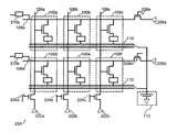
- FIG. 4illustrates a prior art memory device 200 comprising an array of memory cells 100 a - 100 f arranged in rows and columns.
- the memory cells 100 a - 100 f along any given bit line 108 a, 108 bdo not share a common word line 106 a - 106 c.
- the memory cells 100 a - 100 f along any given word line 106 a - 106 cdo not share a common bit line 108 a - 108 b.
- each memory cellis uniquely identified by the combined selection of the word line to which the gate of the memory cell access device is connected, and the bit line to which the source of the memory cell access device is connected.
- Each word line 106 a - 106 cis connected to a word line driver 202 a - 202 c via a respective transistor 204 a - 204 c for selecting the respective word line for an access operation.
- the gates of the transistors 204 a - 204 care used to selectively couple or decouple the word lines 106 a - 106 c to or from the word line drivers 202 a - 202 c.
- each bit line 108 a, 108 bis coupled to a driver 206 a, 206 b via selector gates 208 a, 208 b.
- the current and/or resistance of a selected memory cell 100 a - 100 fis measured by sensor amplifiers 210 a, 210 b connected respectively to the bit lines 108 a, 108 b.
- FIG. 4illustrates a memory array having only two rows of memory cells 100 on two bit lines 108 a - 108 b and three columns of memory cells 100 on three word lines 106 a - 106 c.
- memory deviceswould have significantly more cells in an array.
- an actual memory devicemay include several million memory cells 100 arranged in a number of subarrays.
- variable resistance materialWhile the overall operating scheme of the memory device 200 may be similar regardless of the type of variable resistance material used in the memory elements, much research has focused on memory devices using memory elements having doped chalcogenide materials as the variable resistance material. More specifically, memory cells having a variable resistance material formed of germanium-selenide glass having a stoichiometry of Ge x Se (100 ⁇ x) , with x ranging from about 20 to about 43, which are doped with metal ions, have been shown to be particularly promising for providing a viable commercial alternative to traditional random-access memory devices.
- a metal ion doped chalcogenide variable resistance memory cell having such stoichiometryhas an initial “off” state resistance of over 100 k (for example, 1 M ).
- a voltage having at least a threshold potentialis applied to the electrode serving as the anode, with the cathode held at the reference potential or ground.
- the new resistance of the memory cellis less than 100 k (for example, 20 k ). The cell is considered to be in the “on” state while in the low-resistive state.
- variable resistance memory cellretains this new lower level of resistivity until the resistivity is changed by another qualifying voltage level applied to one of the electrodes of the cell. For example, the memory cell is returned to the high resistance state by applying an erase voltage thereto in the negative direction of the voltage applied in the write operation (to achieve the lower resistance state).
- the erase voltagemay or may not be the same magnitude as the write voltage, but is at least of the same order of magnitude.
- Such chalcogenide variable resistance memory cellscan retain a low-resistance state for several hours, days, or even weeks and are relatively non-volatile compared with typical random-access memory devices.
- metal ion doped chalcogenide variable resistance memory cells in the high resistance stateare completely non-volatile, variable resistance memory cells written to the low resistive state may gradually lose their conductivity across the chalcogenide glass layer and drift towards the high resistive state after an extended period of time.
- metal ion doped chalcogenide variable resistance memory deviceswhich are written using write voltages with pulse widths of less than 100 ns have a tendency to gradually lose their low resistance characteristic in as little as a week. Accordingly, such variable resistance memory devices may require some intermittent refreshing to maintain optimal operation of the devices.
- metal ion doped chalcogenide variable resistance memory cellsmay require an occasional reset operation to reset the bistable resistance levels. Over time, the resistance levels resulting from application of various threshold voltages tend to drift.
- the driffing voltage/resistance (V/R) relationshipis further explained below in the context of write and erase operations via measured voltage/resistance curves..
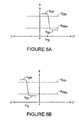
- FIG. 6AA standard voltage/resistance curve for a write operation performed on a properly functioning metal ion doped chalcogenide variable resistance memory cell is illustrated in FIG. 6A .
- a voltage/resistance curvesuch as that shown in FIG. 6A , is derived by measuring the resistance across the chalcogenide variable resistance memory cell as a function of voltage for a given current.
- the initial or normal resistance level of a chalcogenide variable resistance memory cellis shown as R OFF , which is above a minimum threshold level R EMin in which the chalcogenide variable resistance memory cell is stable in a high resistance state.
- FIG. 5Bshows the same programming circuit 300 illustrated in FIG. 5A , except that an erase voltage V TE is applied to the bottom electrode 114 to illustrate an erase operation.
- V TEhas a voltage level of ⁇ 0.75 V and a pulse width of about 8 ns.
- the chalcogenide variable resistance memory cell 310Upon the application of V TE to the bottom electrode 114 of the chalcogenide variable resistance memory cell 310 , the chalcogenide variable resistance memory cell 310 returns to its high resistance (“off”) state, thus erasing the binary value of “1” previously written in the cell, so that the value of “0” is again stored in the chalcogenide variable resistance memory cell 310 .
- FIG. 6Bshows a typical voltage-resistance curve for a metal ion doped chalcogenide variable resistance memory cell during an erase operation.
- R ONindicates the resistance level of the memory cell in the low resistance (“on”) state
- R WMaxrepresents the maximum resistance value at which the memory cell is stable in the low resistance state
- R OFFindicates a resistance level of the memory cell in the high resistance (“off”) state
- R EMindemonstrates the minimum resistance value at which the memory cell is stable in the high resistance state.
- the resistance profiles of metal ion doped chalcogenide variable resistance memory cellshave a tendency to shift after a number of read or write operations have been applied to the cell.
- the cellmay eventually be written into an “on” state in which the resistance in that state is unacceptably high or unacceptably low, or an erase operation may place the cell in an “off” state in which the resistance in that state is unacceptably low or unacceptably high. This can happen in as few as about 400 write and erase cycles. Typical life expectancies for random access memory devices are on the order of 10 14 write/erase cycles. Thus, the resistance drift should be corrected for longevity of operation of the memory cell.
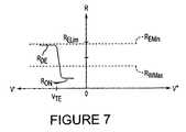
- FIG. 7depicts the case when the chalcogenide variable resistance memory cell drifts towards a low resistance “off” state R DE , meaning that after repeated cycles over time, the “off” state resistance achieved upon application of the fixed erase voltage V TE falls below the level R OFF shown in FIG. 6B .
- the memory cellexhibits an unusually low resistance “on” state R ON .
- the resistance R ONbecomes progressively more variable and drifts increasingly lower upon the performance of repeated erase cycles until application of the threshold erase voltage V TE is consistently insufficient to bring the memory cell to the minimum stable high resistance level R EMin , as illustrated in FIG. 6 .
- a solution to the voltage/resistance curve shift problem described above and illustrated in FIG. 7is to periodically reset the memory cells to an original high resistance level.
- An applied reset or “hard” erase pulseserves to reestablish the original resistance profile of the memory cell in the high resistance state.
- the “hard” erase pulsemay be applied by increasing the voltage level and/or the pulse width relative to erase voltage V TE applied in a normal erase operation.
- a “normal” erase pulseis illustrated in FIG. 8A having, for example, a voltage level of ⁇ 0.8 V and a duration of 8 ns.
- a first type of “hard” erase pulseis shown in FIG.
- FIG. 8BAn alternative “hard” erase pulse is shown in FIG. 8C , in which the “hard” erase pulse has the same magnitude as the normal erase pulse, but has a longer pulse width.
- the “hard” erase pulsemay have both a greater magnitude and a longer duration than the normal erase pulse. The amount by which the voltage level or the duration of the “hard” erase pulse exceeds that of the normal erase pulse may vary depending on the amount of drift, or the amount by which R DE falls below R EMin .
- FIGS. 9A, 9B and 9 CA significant challenge exists in determining an appropriate magnitude of an applied “hard” erase voltage pulse, as illustrated in FIGS. 9A, 9B and 9 C.
- a proposed metal ion doped chalcogenide variable resistance memory cell 500is depicted in FIG. 9B , comprising a p-doped substrate 526 and two n-wells 520 , 522 .
- An access device 502is depicted as a transistor, and is shown in both FIGS. 9A and 9B .
- the access device 502is activated by an “on” word line 506 (i.e., a word line having a voltage sufficient to activate access device 502 ), which is connected to the gate of the transistor.
- the active access device 502allows current to flow between the bit line 508 (connected to the source of the transistor) and the cell plate 510 (connected through the variable resistance memory element 504 to the drain of the transistor). In other words, when the access device 502 is activated, current must flow through two series resistances (refer to FIG. 9C ).
- One resistance, the cell resistance, R cellis highly variable, due to the drifting R ON and R DE levels, as described in detail above.
- R cellcan range anywhere from 5 k• to 46 k•.
- the other resistance that must be accounted foris the channel resistance, R channel , which is generally about 30 k•.
- V cell( V BL - V cpin ) * R cell R cell + R channel Eq . ⁇ 1
- V cellwill range from 0.23 V to 0.97 V as a result of the variable resistance of R cell .
- a normal “hard” erase voltage applied to V BL and V cpinmay not create a sufficient differential to actually reset the chalcogenide variable resistance memory cell.
- a method of erasing a chalcogenide variable resistance memory cellincludes a p-doped substrate with an n-well and a chalcogenide variable resistance memory element.
- the methodincludes the step of applying to the chalcogenide variable resistance memory element a voltage that is less than a fixed voltage of the substrate.
- the applied voltageinduces an erase current to flow from the substrate through the n-well and through the chalcogenide variable resistance memory element.
- the voltagemay be applied to a single chalcogenide variable resistance memory cell, or to an array of chalcogenide variable resistance memory cells, resulting in the erasure of the entire array.
- the voltagemay be applied periodically in order to reset the chalcogenide variable resistance memory cells, or it may be applied only upon power-up or power-down operations.
- the voltagemay also be applied to chalcogenide variable resistance memory cells whose voltage-resistance curves have shifted below a minimum erasure resistance level.
- the substrateacts as a diode when current flows across the substrate, thus making the resistance across the substrate independent of the resistance across the chalcogenide variable resistance memory elements.
- a chalcogenide variable resistance memory devicean array of chalcogenide variable resistance memory devices, and a processing system that includes at least one array of chalcogenide variable resistance memory devices are provided.
- the chalcogenide variable resistance memory devicesare such that the application, to the chalcogenide variable resistance memory element, of a voltage that is less than a fixed voltage of the substrate induces an erase current to flow from the substrate through the chalcogenide variable resistance memory element.
- FIG. 1shows a basic composition of a prior art variable resistance memory cell
- FIG. 2is a prior art variable resistance memory cell with access device
- FIG. 3shows the physical structure of a prior art variable resistance memory cell
- FIG. 4is a prior art memory device comprising variable resistance memory cells
- FIGS. 5A and 5Bare illustrations of prior art chalcogenide variable resistance memory programming circuits
- FIGS. 6A and 6Bare illustrations of standard voltage-resistance curves for a chalcogenide variable resistance memory cell
- FIG. 7is an illustration of a shifted voltage-resistance curve for a chalcogenide variable resistance memory cell
- FIGS. 8A, 8B and 8 Care illustrations of erase pulses for a chalcogenide variable resistance memory cell
- FIGS. 9A, 9B and 9 Cshow an access device with a chalcogenide variable resistance memory cell illustrating a voltage divider circuit
- FIGS. 10A and 10Bshow a chalcogenide variable resistance memory cell constructed in accordance with an exemplary embodiment of the invention.
- FIG. 11is a processor system incorporating chalcogenide variable resistance memory cells, in accordance with an exemplary embodiment of the invention.
- a chalcogenide variable resistance memory cellis subject to an erase operation.
- a voltage differentialmust be created across the chalcogenide variable resistance memory element 104 to induce a current capable of changing the resistance of the chalcogenide variable resistance memory element 104 .
- the necessary erasing currenthas been generated by raising the voltage potential of bit line 108 to a level higher than the voltage potential of cell plate 110 .
- the chalcogenide variable memory cell 600includes a p-doped substrate 626 , two n-wells 620 , 622 , and an access device 602 or transistor whose gate is connected to a word line 606 , whose source is connected to a bit line 608 , and whose drain is connected to the chalcogenide variable resistance memory element 604 .
- a voltage, V BBis shown, representing the fixed voltage of the substrate 626 .
- V cpinIf the cell plate 610 voltage, V cpin , is lowered to a level that is less than V BB , and if the word line 606 is maintained in an “off” state, then a current may be induced to flow from the substrate 626 to the cell plate 610 and through the chalcogenide variable resistance memory element 604 . This current, if strong enough, could effectuate an erase operation.
- V cellV BB ⁇ V cpin ⁇ V diode Eq. 2 V cpin is easily adjusted in order to obtain the desired V cell . Additionally, because of the relative constancy of V diode , V cell is independent of R cell .
- the above-described embodiment of the inventionmay be used to simultaneously perform erase operations on multiple or even all memory cells in a memory array such as that shown in FIG. 4 .
- V BBis the same.
- V cpinis lowered to a voltage level less than V BB for each chalcogenide variable resistance memory cell that is to be erased.
- Single memory cellsmay be erased. More commonly, entire rows or even blocks of memory cells may be erased. If desired the entire array of memory cells may be erased simultaneously.
- the described erase methodis used as a standard full array erase operation every time an erase operation is necessary.
- the erase methodis used to reset the resistances of the chalcogenide variable resistance memory cells periodically, for example, every 10 or 100 memory cycles, wherein a memory cycle is the amount of time required for a memory to complete a read or write operation.
- the erase methodcould be used on power-up or power-down of a memory array.
- the erase methodcould be used on individual chalcogenide variable resistance memory cells in order to repair (via an erase operation) memory cells whose measured voltage-resistance curves have drifted out of the range in which a traditional erase operation is effective.
- the voltage/resistance curves of each cellcould be measured by measuring the resistance of the cells as a function of applied voltage for a given current.
- the voltage/resistance curve for a given memory cellhas slipped below a threshold minimal erase level (as demonstrated in FIG. 7 ) when the cell no longer responds to other proposed erase methods (such as the method of FIG. 9 ). If a non-responsive memory cell is observed via parity checking or other error-revealing methods, then either the one non-responsive memory cell or an entire block of memory cells that contains the non-responsive memory cell may be erased and reset using the disclosed erase method.
- FIG. 11illustrates a typical processor system 1000 which includes a memory circuit 1040 such as a chalcogenide variable resistance memory device, which employs chalcogenide variable resistance memory cells fabricated in accordance with the invention.
- a processor systemsuch as a computer system, generally comprises a central processing unit (CPU) 1010 , such as a microprocessor, a digital signal processor, or other programmable digital logic devices, which communicates with an input/output (I/O) device 1020 over a bus 1090 .
- the memory circuit 1040communicates with the CPU 1010 over bus 1090 typically through a memory controller.
- the processor systemmay include peripheral devices such as removable media devices 1050 which communicate with CPU 1010 over the bus 1090 .
- Memory circuit 1040is preferably constructed as an integrated circuit, which includes one or more resistance variable memory devices. If desired, the memory circuit 1040 may be combined with the processor, for example CPU 1010 , in a single integrated circuit.
Landscapes
- Semiconductor Memories (AREA)
Abstract
Description
- The invention relates generally to the field of semiconductor devices and, more particularly, to variable resistance memory devices.
- Microprocessor-accessible memory devices have traditionally been classified as either non-volatile or volatile memory devices. Non-volatile memory devices are capable of retaining stored information even when power to the memory device is turned off. However, non-volatile memory devices occupy a large amount of space and consume large quantities of power, making these devices unsuitable for use in portable devices or as substitutes for frequently-accessed volatile memory devices. On the other hand, volatile memory devices tend to provide greater storage capability and programming options than non-volatile memory devices. Volatile memory devices also generally consume less power than non-volatile devices. However, volatile memory devices require a continuous power supply in order to retain stored memory content.
- Commercially viable memory devices that are both randomly accessed and semi-volatile or non-volatile are desired. Various implementations of such semi-volatile and nonvolatile random access memory devices are being developed. These devices store data in a plurality of memory cells by structurally or chemically changing the resistance across the memory cells in response to predetermined voltages applied to the memory cells. Examples of variable resistance memory devices being investigated include memories using variable resistance polymers, perovskite, doped amorphous silicon, phase-changing glasses, or doped chalcogenide glass, among others.
- In a variable resistance memory cell, a first value may be written to the variable resistance memory cell by applying a voltage having a predetermined level. The applied voltage changes the electrical resistance across the memory cell. A second value, or the default value, may be written or restored in the memory cell by applying a second voltage to the memory cell, thereby changing the resistance across the memory cell to the original resistance level. The second voltage is typically a negative voltage in comparison to the first voltage and may or may not have the same magnitude as the first voltage. Each resistance state is stable, so that the memory cells are capable of retaining their stored values without being frequently refreshed. The variable resistance materials can thus be “programmed” to any of the stable resistance values.
- The content of a variable resistance memory cell is read or “accessed” by applying a read voltage to determine the resistance level across the cell. The magnitude of the read voltage is lower than the magnitude of the voltage required to change the resistance of the variable resistance memory cell. In a binary variable resistance memory cell, upon determining the resistance level of the variable resistance memory cell, the detected resistance level is compared with a reference resistance level. Generally, if the detected resistance level is greater than the reference level, the memory cell is determined to be in the “off” state. On the other hand, if the detected resistance level is less than the reference level, the memory cell is determined to be in the “on” state.
FIG. 1 shows a basic composition of a variableresistance memory cell 10 constructed over asubstrate 12, having avariable resistance material 16 formed between twoelectrodes electrodes - In
FIG. 2 , a typical prior art variableresistance memory cell 100 is shown to include anaccess device 102, a variableresistance memory element 104, and acell plate 110. Theaccess device 102 is a transistor having agate 102acoupled to aword line 106 and one terminal (source)102bcoupled to a bit line108. The other terminal (drain)102cof theaccess device 102 is coupled to one end of the variableresistance memory element 104, while the other end of the variableresistance memory element 104 is coupled to thecell plate 110. Thecell plate 110 may span and be coupled to several other variable resistance memory cells, and may form the anode of all thememory elements 104 in an array of variable resistance memory cells. Thecell plate 110 is also coupled to apotential source 112. - A representative diagram of the physical structure of the prior
art memory cell 100 is shown inFIG. 3 . In particular, a p-dopedsubstrate 126 includes two n-wells Access device 102 is formed on the surface of thesubstrate 126 between the two n-wells wells source 102banddrain 102c,respectively, of theaccess device 102.Word line 106 is formed as a conductive strip extending into the page across the top ofaccess device 102. Bit line108 is connected directly to the n-well120 forming thesource 102bof theaccess device 102. Variableresistance memory element 104 is formed on the substrate with itscathode 114 in contact with n-well 122 and the cell plate110 (only a portion of which is shown) as its anode. Thecell plate 110 ofmemory element 104 is connected to apotential source 112. - In the conventional operating scheme for the
cell 100, when thememory element 104 is idle, the voltage across theanode 110 and thecathode 114 is below a threshold voltage VG. The value of the threshold voltage VGis a function of the specific variable resistance material used in thememory element 104. In order to perform any access operations including programming the variableresistance memory element 104 to the low resistance state, erasing a programmed variableresistance memory element 104 by returning the variableresistance memory element 104 to the high resistance state, or reading the value stored inmemory element 104, the threshold voltage VGmust be applied to theword line 106. The voltage VGon theword line 106 activates thegate 102aof theaccess device 102 so that an n-channel is formed in thesubstrate 126 under the gate structure of theaccess device 102 and across the gap between the two n-wells access device 102 . Upon activating theaccess device 102, thememory element 104 can be programmed to the low resistance state by applying a write (positive) voltage having at least the magnitude of a threshold voltage VTWacross thememory element 104. - In conventional operating schemes, application of the write voltage may be achieved by raising the potential at the cell plate110 (anode) relative to the
access device drain 102bby applying or raising the voltage at thepotential source 112, lowering the potential of the bit line108, or a combination of both. To erase a programmedmemory element 104, a negative voltage having a magnitude of at least a threshold erase voltage is applied between the anode and the cathode of thememory element 104, such that the potential at thecell plate 110 is lower than the potential of the bit line108. - Variable resistance memory cells are arranged as an array of memory cells and are written, erased, and read using a controller.
FIG. 4 illustrates a priorart memory device 200 comprising an array ofmemory cells 100a-100farranged in rows and columns. Thememory cells 100a-100falong any givenbit line common word line 106a-106c.Conversely, thememory cells 100a-100falong any givenword line 106a-106cdo not share a common bit line108a-108b.In this manner, each memory cell is uniquely identified by the combined selection of the word line to which the gate of the memory cell access device is connected, and the bit line to which the source of the memory cell access device is connected. - Each
word line 106a-106cis connected to a word line driver202a-202cvia a respective transistor204a-204cfor selecting the respective word line for an access operation. The gates of the transistors204a-204care used to selectively couple or decouple theword lines 106a-106cto or from the word line drivers202a-202c.Similarly, eachbit line driver selector gates memory cell 100a-100fis measured bysensor amplifiers bit lines - For simplicity,
FIG. 4 illustrates a memory array having only two rows ofmemory cells 100 on two bit lines108a-108band three columns ofmemory cells 100 on threeword lines 106a-106c.However, it should be understood that in practical applications, memory devices would have significantly more cells in an array. For example, an actual memory device may include several millionmemory cells 100 arranged in a number of subarrays. - While the overall operating scheme of the
memory device 200 may be similar regardless of the type of variable resistance material used in the memory elements, much research has focused on memory devices using memory elements having doped chalcogenide materials as the variable resistance material. More specifically, memory cells having a variable resistance material formed of germanium-selenide glass having a stoichiometry of GexSe(100−x), with x ranging from about 20 to about 43, which are doped with metal ions, have been shown to be particularly promising for providing a viable commercial alternative to traditional random-access memory devices. - Generally, a metal ion doped chalcogenide variable resistance memory cell having such stoichiometry has an initial “off” state resistance of over 100 k (for example, 1 M ). To perform a write operation on a chalcogenide memory cell in its normal high resistive state, a voltage having at least a threshold potential is applied to the electrode serving as the anode, with the cathode held at the reference potential or ground. Upon applying the threshold level or write voltage, the resistance across the memory cell changes to a level dramatically reduced from the resistance in its normal state. The new resistance of the memory cell is less than 100 k (for example, 20 k ). The cell is considered to be in the “on” state while in the low-resistive state.
- The variable resistance memory cell retains this new lower level of resistivity until the resistivity is changed by another qualifying voltage level applied to one of the electrodes of the cell. For example, the memory cell is returned to the high resistance state by applying an erase voltage thereto in the negative direction of the voltage applied in the write operation (to achieve the lower resistance state). The erase voltage may or may not be the same magnitude as the write voltage, but is at least of the same order of magnitude.
- Such chalcogenide variable resistance memory cells can retain a low-resistance state for several hours, days, or even weeks and are relatively non-volatile compared with typical random-access memory devices. However, while metal ion doped chalcogenide variable resistance memory cells in the high resistance state are completely non-volatile, variable resistance memory cells written to the low resistive state may gradually lose their conductivity across the chalcogenide glass layer and drift towards the high resistive state after an extended period of time. In particular, it has been found that metal ion doped chalcogenide variable resistance memory devices which are written using write voltages with pulse widths of less than 100 ns have a tendency to gradually lose their low resistance characteristic in as little as a week. Accordingly, such variable resistance memory devices may require some intermittent refreshing to maintain optimal operation of the devices.
- In addition to intermittent refresh operations, metal ion doped chalcogenide variable resistance memory cells may require an occasional reset operation to reset the bistable resistance levels. Over time, the resistance levels resulting from application of various threshold voltages tend to drift. The driffing voltage/resistance (V/R) relationship is further explained below in the context of write and erase operations via measured voltage/resistance curves..
- A standard voltage/resistance curve for a write operation performed on a properly functioning metal ion doped chalcogenide variable resistance memory cell is illustrated in
FIG. 6A . A voltage/resistance curve, such as that shown inFIG. 6A , is derived by measuring the resistance across the chalcogenide variable resistance memory cell as a function of voltage for a given current. The initial or normal resistance level of a chalcogenide variable resistance memory cell is shown as ROFF, which is above a minimum threshold level REMinin which the chalcogenide variable resistance memory cell is stable in a high resistance state. When the chalcogenide variable resistance memory cell is in the high resistance state and VTWis applied to the cell, the resistance drops to the level indicated by RON, which is below a maximum threshold level RWMaxin which the chalcogenide variable resistance memory cell is stable in a low resistance state. FIG. 5B shows thesame programming circuit 300 illustrated inFIG. 5A , except that an erase voltage VTEis applied to thebottom electrode 114 to illustrate an erase operation. By way of example, VTEhas a voltage level of −0.75 V and a pulse width of about 8 ns. Upon the application of VTEto thebottom electrode 114 of the chalcogenide variableresistance memory cell 310, the chalcogenide variableresistance memory cell 310 returns to its high resistance (“off”) state, thus erasing the binary value of “1” previously written in the cell, so that the value of “0” is again stored in the chalcogenide variableresistance memory cell 310.FIG. 6B shows a typical voltage-resistance curve for a metal ion doped chalcogenide variable resistance memory cell during an erase operation. As inFIG. 6A , RONindicates the resistance level of the memory cell in the low resistance (“on”) state, and RWMaxrepresents the maximum resistance value at which the memory cell is stable in the low resistance state, while ROFFindicates a resistance level of the memory cell in the high resistance (“off”) state, and REMindemonstrates the minimum resistance value at which the memory cell is stable in the high resistance state. When the metal ion doped chalcogenide variable resistance memory cell is in the low resistance state and VTEis subsequently applied to the cell, the resistance in the chalcogenide variable resistance memory cell increases to the level indicated by ROFF. It is noted that the write voltage VTWis not necessarily of the same magnitude as the erase voltage VTE.- However, as mentioned above, the resistance profiles of metal ion doped chalcogenide variable resistance memory cells have a tendency to shift after a number of read or write operations have been applied to the cell. Specifically, the cell may eventually be written into an “on” state in which the resistance in that state is unacceptably high or unacceptably low, or an erase operation may place the cell in an “off” state in which the resistance in that state is unacceptably low or unacceptably high. This can happen in as few as about 400 write and erase cycles. Typical life expectancies for random access memory devices are on the order of 1014write/erase cycles. Thus, the resistance drift should be corrected for longevity of operation of the memory cell.
- The phenomenon of resistance drift is demonstrated in
FIG. 7 , which depicts the case when the chalcogenide variable resistance memory cell drifts towards a low resistance “off” state RDE, meaning that after repeated cycles over time, the “off” state resistance achieved upon application of the fixed erase voltage VTEfalls below the level ROFFshown inFIG. 6B . Similarly, the memory cell exhibits an unusually low resistance “on” state RON. The resistance RONbecomes progressively more variable and drifts increasingly lower upon the performance of repeated erase cycles until application of the threshold erase voltage VTEis consistently insufficient to bring the memory cell to the minimum stable high resistance level REMin, as illustrated inFIG. 6 . Once this condition is reached, subsequent erase operations will fail to erase the stored value in the chalcogenide variable resistance memory cell, causing a breakdown in the ftmction of the chalcogenide variable resistance memory device. Additionally, continued write cycles applied to these already low resistance state memory cells result in pushing the memory cells into an even lower resistance state. - A solution to the voltage/resistance curve shift problem described above and illustrated in
FIG. 7 is to periodically reset the memory cells to an original high resistance level. An applied reset or “hard” erase pulse serves to reestablish the original resistance profile of the memory cell in the high resistance state. The “hard” erase pulse may be applied by increasing the voltage level and/or the pulse width relative to erase voltage VTEapplied in a normal erase operation. A “normal” erase pulse is illustrated inFIG. 8A having, for example, a voltage level of −0.8 V and a duration of 8 ns. A first type of “hard” erase pulse is shown inFIG. 8B , in which the applied pulse is the same duration as the normal erase pulse, but has a negative voltage level of a magnitude greater than the −0.8 V of the normal erase pulse. An alternative “hard” erase pulse is shown inFIG. 8C , in which the “hard” erase pulse has the same magnitude as the normal erase pulse, but has a longer pulse width. In a further alternative, the “hard” erase pulse may have both a greater magnitude and a longer duration than the normal erase pulse. The amount by which the voltage level or the duration of the “hard” erase pulse exceeds that of the normal erase pulse may vary depending on the amount of drift, or the amount by which RDEfalls below REMin. - A significant challenge exists in determining an appropriate magnitude of an applied “hard” erase voltage pulse, as illustrated in
FIGS. 9A, 9B and9C. A proposed metal ion doped chalcogenide variableresistance memory cell 500 is depicted inFIG. 9B , comprising a p-dopedsubstrate 526 and two n-wells access device 502 is depicted as a transistor, and is shown in bothFIGS. 9A and 9B . Theaccess device 502 is activated by an “on” word line506 (i.e., a word line having a voltage sufficient to activate access device502), which is connected to the gate of the transistor. Theactive access device 502 allows current to flow between the bit line508 (connected to the source of the transistor) and the cell plate510 (connected through the variableresistance memory element 504 to the drain of the transistor). In other words, when theaccess device 502 is activated, current must flow through two series resistances (refer toFIG. 9C ). One resistance, the cell resistance, Rcell, is highly variable, due to the drifting RONand RDElevels, as described in detail above. Typically, Rcellcan range anywhere from 5 k• to 46 k•. The other resistance that must be accounted for is the channel resistance, Rchannel, which is generally about 30 k•. With both resistances Rcell, Rchannelin series, a voltage divider equation must be solved in order to determine the voltage across the chalcogenide variableresistance memory cell 504. - Using Equation 1, and setting (for purposes of example only) VBLto equal 2.2 V and Vcpinto equal 0.6 V, the value of Vcellwill range from 0.23 V to 0.97 V as a result of the variable resistance of Rcell. In other words, if the resistance-voltage curve for the chalcogenide variable resistance memory cell has drifted too low, as shown in
FIG. 7 , then a normal “hard” erase voltage applied to VBLand Vcpinmay not create a sufficient differential to actually reset the chalcogenide variable resistance memory cell. - From the discussion above, it should be appreciated that an improved method for effectuating a “hard” erase of a chalcogenide variable resistance memory cell is both needed and desired.
- In one embodiment of the invention, a method of erasing a chalcogenide variable resistance memory cell is provided. The chalcogenide variable resistance memory cell includes a p-doped substrate with an n-well and a chalcogenide variable resistance memory element. The method includes the step of applying to the chalcogenide variable resistance memory element a voltage that is less than a fixed voltage of the substrate. The applied voltage induces an erase current to flow from the substrate through the n-well and through the chalcogenide variable resistance memory element. The voltage may be applied to a single chalcogenide variable resistance memory cell, or to an array of chalcogenide variable resistance memory cells, resulting in the erasure of the entire array. The voltage may be applied periodically in order to reset the chalcogenide variable resistance memory cells, or it may be applied only upon power-up or power-down operations. The voltage may also be applied to chalcogenide variable resistance memory cells whose voltage-resistance curves have shifted below a minimum erasure resistance level. When the voltage is applied, the substrate acts as a diode when current flows across the substrate, thus making the resistance across the substrate independent of the resistance across the chalcogenide variable resistance memory elements.
- In other embodiments of the invention, a chalcogenide variable resistance memory device, an array of chalcogenide variable resistance memory devices, and a processing system that includes at least one array of chalcogenide variable resistance memory devices are provided. The chalcogenide variable resistance memory devices are such that the application, to the chalcogenide variable resistance memory element, of a voltage that is less than a fixed voltage of the substrate induces an erase current to flow from the substrate through the chalcogenide variable resistance memory element.
- These and other aspects of the invention will be more clearly recognized from the following detailed description of the invention which is provided in connection with the accompanying drawings.
FIG. 1 shows a basic composition of a prior art variable resistance memory cell;FIG. 2 is a prior art variable resistance memory cell with access device;FIG. 3 shows the physical structure of a prior art variable resistance memory cell;FIG. 4 is a prior art memory device comprising variable resistance memory cells;FIGS. 5A and 5B are illustrations of prior art chalcogenide variable resistance memory programming circuits;FIGS. 6A and 6B are illustrations of standard voltage-resistance curves for a chalcogenide variable resistance memory cell;FIG. 7 is an illustration of a shifted voltage-resistance curve for a chalcogenide variable resistance memory cell;FIGS. 8A, 8B and8C are illustrations of erase pulses for a chalcogenide variable resistance memory cell;FIGS. 9A, 9B and9C show an access device with a chalcogenide variable resistance memory cell illustrating a voltage divider circuit;FIGS. 10A and 10B show a chalcogenide variable resistance memory cell constructed in accordance with an exemplary embodiment of the invention; andFIG. 11 is a processor system incorporating chalcogenide variable resistance memory cells, in accordance with an exemplary embodiment of the invention.- In the following detailed description, reference is made to various specific structural and process embodiments of the invention. These embodiments are described with sufficient detail to enable those skilled in the art to practice the invention. It is to be understood that other embodiments may be employed, and that various structural, logical and electrical changes may be made without departing from the spirit or scope of the invention.
- According to the invention, a chalcogenide variable resistance memory cell is subject to an erase operation. In order to erase a chalcogenide variable resistance memory cell, such as that shown in
FIG. 3 , a voltage differential must be created across the chalcogenide variableresistance memory element 104 to induce a current capable of changing the resistance of the chalcogenide variableresistance memory element 104. Traditionally, as explained above, the necessary erasing current has been generated by raising the voltage potential of bit line108 to a level higher than the voltage potential ofcell plate 110. Then, whenword line 106 was activated, thus activating theaccess device 102, an erase current would flow through theaccess device 102 and the chalcogenide variableresistance memory element 104 from bit line108 tocell plate 110. However, the inventor has determined that if, as is described below, current were to flow instead from and through thesubstrate 126 to thecell plate 110, the prior art voltage-divider problem would be avoided. - Referring now to
FIG. 10A , wherein a chalcogenidevariable memory cell 600 is shown, an embodiment of the invention is depicted. As in the traditional chalcogenide variable resistance memory devices, the chalcogenidevariable memory cell 600 includes a p-dopedsubstrate 626, two n-wells access device 602 or transistor whose gate is connected to aword line 606, whose source is connected to abit line 608, and whose drain is connected to the chalcogenide variableresistance memory element 604. A voltage, VBB, is shown, representing the fixed voltage of thesubstrate 626. If thecell plate 610 voltage, Vcpin, is lowered to a level that is less than VBB, and if theword line 606 is maintained in an “off” state, then a current may be induced to flow from thesubstrate 626 to thecell plate 610 and through the chalcogenide variableresistance memory element 604. This current, if strong enough, could effectuate an erase operation. - When current flows from the p-doped
substrate 626 to thecell plate 610, the current necessarily passes through the n-well622 acting as a drain for theaccess device 602. The resulting p-n junction behaves as a diode. Thus, instead of the erase current flowing through two series resistances, the erase current flows through a forward-biased diode and one resistance, Rcell(refer toFIG. 10B ). Voltage drops across forward-biased diodes are relatively constant (usually around 0.7 V), and thus the voltage drop across the chalcogenide variableresistance memory element 604 will simply equal the difference between the VBB-Vcpindifferential and the voltage across the diode, Vdiode. This relationship is shown below in Equation 2.
Vcell=VBB−Vcpin−Vdiode Eq. 2
Vcpinis easily adjusted in order to obtain the desired Vcell. Additionally, because of the relative constancy of Vdiode, Vcellis independent of Rcell. - The above-described embodiment of the invention may be used to simultaneously perform erase operations on multiple or even all memory cells in a memory array such as that shown in
FIG. 4 . For each chalcogenide variable resistance memory cell in the array, VBBis the same. Vcpinis lowered to a voltage level less than VBBfor each chalcogenide variable resistance memory cell that is to be erased. Single memory cells may be erased. More commonly, entire rows or even blocks of memory cells may be erased. If desired the entire array of memory cells may be erased simultaneously. - In one embodiment of the invention, the described erase method is used as a standard full array erase operation every time an erase operation is necessary. In another embodiment of the invention, the erase method is used to reset the resistances of the chalcogenide variable resistance memory cells periodically, for example, every 10 or 100 memory cycles, wherein a memory cycle is the amount of time required for a memory to complete a read or write operation. Furthermore, the erase method could be used on power-up or power-down of a memory array. Additionally, the erase method could be used on individual chalcogenide variable resistance memory cells in order to repair (via an erase operation) memory cells whose measured voltage-resistance curves have drifted out of the range in which a traditional erase operation is effective. In theory, the voltage/resistance curves of each cell could be measured by measuring the resistance of the cells as a function of applied voltage for a given current. However, in practice, it may be assumed that the voltage/resistance curve for a given memory cell has slipped below a threshold minimal erase level (as demonstrated in
FIG. 7 ) when the cell no longer responds to other proposed erase methods (such as the method ofFIG. 9 ). If a non-responsive memory cell is observed via parity checking or other error-revealing methods, then either the one non-responsive memory cell or an entire block of memory cells that contains the non-responsive memory cell may be erased and reset using the disclosed erase method. FIG. 11 illustrates atypical processor system 1000 which includes amemory circuit 1040 such as a chalcogenide variable resistance memory device, which employs chalcogenide variable resistance memory cells fabricated in accordance with the invention. A processor system, such as a computer system, generally comprises a central processing unit (CPU)1010, such as a microprocessor, a digital signal processor, or other programmable digital logic devices, which communicates with an input/output (I/O)device 1020 over abus 1090. Thememory circuit 1040 communicates with theCPU 1010 overbus 1090 typically through a memory controller.- In the case of a computer system, the processor system may include peripheral devices such as
removable media devices 1050 which communicate withCPU 1010 over thebus 1090.Memory circuit 1040 is preferably constructed as an integrated circuit, which includes one or more resistance variable memory devices. If desired, thememory circuit 1040 may be combined with the processor, forexample CPU 1010, in a single integrated circuit. - The above description and drawings should only be considered illustrative of exemplary embodiments that achieve the features and advantages of the invention. Modification and substitutions to specific process conditions and structures can be made without departing from the spirit and scope of the invention. Accordingly, the invention is not to be considered as being limited by the foregoing description and drawings, but is only limited by the scope of the appended claims.
Claims (33)
Priority Applications (4)
| Application Number | Priority Date | Filing Date | Title |
|---|---|---|---|
| US11/176,884US7233520B2 (en) | 2005-07-08 | 2005-07-08 | Process for erasing chalcogenide variable resistance memory bits |
| PCT/US2006/025551WO2007008452A1 (en) | 2005-07-08 | 2006-06-30 | Process for erasing chalcogenide variable resistance memory bits |
| TW095124752ATWI303483B (en) | 2005-07-08 | 2006-07-07 | Process for erasing chalcogenide variable resistance memory bits |
| US11/745,209US7643333B2 (en) | 2005-07-08 | 2007-05-07 | Process for erasing chalcogenide variable resistance memory bits |
Applications Claiming Priority (1)
| Application Number | Priority Date | Filing Date | Title |
|---|---|---|---|
| US11/176,884US7233520B2 (en) | 2005-07-08 | 2005-07-08 | Process for erasing chalcogenide variable resistance memory bits |
Related Child Applications (1)
| Application Number | Title | Priority Date | Filing Date |
|---|---|---|---|
| US11/745,209ContinuationUS7643333B2 (en) | 2005-07-08 | 2007-05-07 | Process for erasing chalcogenide variable resistance memory bits |
Publications (2)
| Publication Number | Publication Date |
|---|---|
| US20070008768A1true US20070008768A1 (en) | 2007-01-11 |
| US7233520B2 US7233520B2 (en) | 2007-06-19 |
Family
ID=37076222
Family Applications (2)
| Application Number | Title | Priority Date | Filing Date |
|---|---|---|---|
| US11/176,884Expired - LifetimeUS7233520B2 (en) | 2005-07-08 | 2005-07-08 | Process for erasing chalcogenide variable resistance memory bits |
| US11/745,209Expired - LifetimeUS7643333B2 (en) | 2005-07-08 | 2007-05-07 | Process for erasing chalcogenide variable resistance memory bits |
Family Applications After (1)
| Application Number | Title | Priority Date | Filing Date |
|---|---|---|---|
| US11/745,209Expired - LifetimeUS7643333B2 (en) | 2005-07-08 | 2007-05-07 | Process for erasing chalcogenide variable resistance memory bits |
Country Status (3)
| Country | Link |
|---|---|
| US (2) | US7233520B2 (en) |
| TW (1) | TWI303483B (en) |
| WO (1) | WO2007008452A1 (en) |
Cited By (10)
| Publication number | Priority date | Publication date | Assignee | Title |
|---|---|---|---|---|
| US20070279976A1 (en)* | 2005-03-11 | 2007-12-06 | Gilbert Nad E | Read, write, and erase circuit for programmable memory devices |
| US20080273378A1 (en)* | 2007-05-03 | 2008-11-06 | Jan Boris Philipp | Multi-level resistive memory cell using different crystallization speeds |
| US20080298114A1 (en)* | 2007-05-31 | 2008-12-04 | Micron Technology, Inc. | Phase change memory structure with multiple resistance states and methods of programming an sensing same |
| US20080310208A1 (en)* | 2005-07-08 | 2008-12-18 | Jon Daley | Process for erasing chalcogenide variable resistance memory bits |
| US20090225583A1 (en)* | 2008-03-05 | 2009-09-10 | Samsung Electronics Co., Ltd. | Resistive memory device for programming resistance conversion layers and method thereof |
| US20110069532A1 (en)* | 2009-09-18 | 2011-03-24 | Kabushiki Kaisha Toshiba | Nonvolatile semiconductor memory device |
| WO2011123465A1 (en)* | 2010-03-29 | 2011-10-06 | 4D-S Pty Ltd. | Method and system for utilizing perovskite material for charge storage and as a dielectric |
| CN104658600A (en)* | 2013-11-22 | 2015-05-27 | 旺宏电子股份有限公司 | Memory architecture and operation method thereof |
| US9293201B2 (en) | 2009-08-14 | 2016-03-22 | 4D-S Pty, Ltd | Heterojunction oxide non-volatile memory devices |
| US20170150287A1 (en)* | 2009-11-09 | 2017-05-25 | Samsung Electronics Co., Ltd | Apparatus and method for reproducing multi-sound channel contents using dlna in mobile terminal |
Families Citing this family (29)
| Publication number | Priority date | Publication date | Assignee | Title |
|---|---|---|---|---|
| JP4189395B2 (en)* | 2004-07-28 | 2008-12-03 | シャープ株式会社 | Nonvolatile semiconductor memory device and reading method |
| JP4591821B2 (en)* | 2005-02-09 | 2010-12-01 | エルピーダメモリ株式会社 | Semiconductor device |
| US7635855B2 (en) | 2005-11-15 | 2009-12-22 | Macronix International Co., Ltd. | I-shaped phase change memory cell |
| US7449710B2 (en) | 2005-11-21 | 2008-11-11 | Macronix International Co., Ltd. | Vacuum jacket for phase change memory element |
| US8077495B2 (en)* | 2006-12-05 | 2011-12-13 | Spansion Llc | Method of programming, erasing and repairing a memory device |
| US7718989B2 (en) | 2006-12-28 | 2010-05-18 | Macronix International Co., Ltd. | Resistor random access memory cell device |
| US7729161B2 (en) | 2007-08-02 | 2010-06-01 | Macronix International Co., Ltd. | Phase change memory with dual word lines and source lines and method of operating same |
| JP5214208B2 (en)* | 2007-10-01 | 2013-06-19 | スパンション エルエルシー | Semiconductor device and control method thereof |
| US7990761B2 (en)* | 2008-03-31 | 2011-08-02 | Ovonyx, Inc. | Immunity of phase change material to disturb in the amorphous phase |
| US7701750B2 (en) | 2008-05-08 | 2010-04-20 | Macronix International Co., Ltd. | Phase change device having two or more substantial amorphous regions in high resistance state |
| US7825479B2 (en) | 2008-08-06 | 2010-11-02 | International Business Machines Corporation | Electrical antifuse having a multi-thickness dielectric layer |
| WO2010038442A1 (en)* | 2008-09-30 | 2010-04-08 | パナソニック株式会社 | Method for driving resistance change element, initial processing method, and nonvolatile storage device |
| US8064247B2 (en) | 2009-01-14 | 2011-11-22 | Macronix International Co., Ltd. | Rewritable memory device based on segregation/re-absorption |
| US8406033B2 (en) | 2009-06-22 | 2013-03-26 | Macronix International Co., Ltd. | Memory device and method for sensing and fixing margin cells |
| US8363463B2 (en) | 2009-06-25 | 2013-01-29 | Macronix International Co., Ltd. | Phase change memory having one or more non-constant doping profiles |
| US8238149B2 (en) | 2009-06-25 | 2012-08-07 | Macronix International Co., Ltd. | Methods and apparatus for reducing defect bits in phase change memory |
| US7894254B2 (en) | 2009-07-15 | 2011-02-22 | Macronix International Co., Ltd. | Refresh circuitry for phase change memory |
| US8198619B2 (en) | 2009-07-15 | 2012-06-12 | Macronix International Co., Ltd. | Phase change memory cell structure |
| US8110822B2 (en) | 2009-07-15 | 2012-02-07 | Macronix International Co., Ltd. | Thermal protect PCRAM structure and methods for making |
| US8064248B2 (en) | 2009-09-17 | 2011-11-22 | Macronix International Co., Ltd. | 2T2R-1T1R mix mode phase change memory array |
| US8178387B2 (en) | 2009-10-23 | 2012-05-15 | Macronix International Co., Ltd. | Methods for reducing recrystallization time for a phase change material |
| US8729521B2 (en) | 2010-05-12 | 2014-05-20 | Macronix International Co., Ltd. | Self aligned fin-type programmable memory cell |
| US8310864B2 (en) | 2010-06-15 | 2012-11-13 | Macronix International Co., Ltd. | Self-aligned bit line under word line memory array |
| US8395935B2 (en) | 2010-10-06 | 2013-03-12 | Macronix International Co., Ltd. | Cross-point self-aligned reduced cell size phase change memory |
| US8497705B2 (en) | 2010-11-09 | 2013-07-30 | Macronix International Co., Ltd. | Phase change device for interconnection of programmable logic device |
| US8467238B2 (en) | 2010-11-15 | 2013-06-18 | Macronix International Co., Ltd. | Dynamic pulse operation for phase change memory |
| JP5634367B2 (en)* | 2011-09-26 | 2014-12-03 | 株式会社東芝 | Semiconductor memory device |
| US9336878B2 (en)* | 2014-06-18 | 2016-05-10 | Macronix International Co., Ltd. | Method and apparatus for healing phase change memory devices |
| US9672906B2 (en) | 2015-06-19 | 2017-06-06 | Macronix International Co., Ltd. | Phase change memory with inter-granular switching |
Citations (92)
| Publication number | Priority date | Publication date | Assignee | Title |
|---|---|---|---|---|
| US3961314A (en)* | 1974-03-05 | 1976-06-01 | Energy Conversion Devices, Inc. | Structure and method for producing an image |
| US3966317A (en)* | 1974-04-08 | 1976-06-29 | Energy Conversion Devices, Inc. | Dry process production of archival microform records from hard copy |
| US4267261A (en)* | 1971-07-15 | 1981-05-12 | Energy Conversion Devices, Inc. | Method for full format imaging |
| US4269935A (en)* | 1979-07-13 | 1981-05-26 | Ionomet Company, Inc. | Process of doping silver image in chalcogenide layer |
| US4312938A (en)* | 1979-07-06 | 1982-01-26 | Drexler Technology Corporation | Method for making a broadband reflective laser recording and data storage medium with absorptive underlayer |
| US4316946A (en)* | 1979-12-03 | 1982-02-23 | Ionomet Company, Inc. | Surface sensitized chalcogenide product and process for making and using the same |
| US4320191A (en)* | 1978-11-07 | 1982-03-16 | Nippon Telegraph & Telephone Public Corporation | Pattern-forming process |
| US4499557A (en)* | 1980-10-28 | 1985-02-12 | Energy Conversion Devices, Inc. | Programmable cell for use in programmable electronic arrays |
| US4637895A (en)* | 1985-04-01 | 1987-01-20 | Energy Conversion Devices, Inc. | Gas mixtures for the vapor deposition of semiconductor material |
| US4646266A (en)* | 1984-09-28 | 1987-02-24 | Energy Conversion Devices, Inc. | Programmable semiconductor structures and methods for using the same |
| US4664939A (en)* | 1985-04-01 | 1987-05-12 | Energy Conversion Devices, Inc. | Vertical semiconductor processor |
| US4668968A (en)* | 1984-05-14 | 1987-05-26 | Energy Conversion Devices, Inc. | Integrated circuit compatible thin film field effect transistor and method of making same |
| US4670763A (en)* | 1984-05-14 | 1987-06-02 | Energy Conversion Devices, Inc. | Thin film field effect transistor |
| US4671618A (en)* | 1986-05-22 | 1987-06-09 | Wu Bao Gang | Liquid crystalline-plastic material having submillisecond switch times and extended memory |
| US4673957A (en)* | 1984-05-14 | 1987-06-16 | Energy Conversion Devices, Inc. | Integrated circuit compatible thin film field effect transistor and method of making same |
| US4728406A (en)* | 1986-08-18 | 1988-03-01 | Energy Conversion Devices, Inc. | Method for plasma - coating a semiconductor body |
| US4737379A (en)* | 1982-09-24 | 1988-04-12 | Energy Conversion Devices, Inc. | Plasma deposited coatings, and low temperature plasma method of making same |
| US4795657A (en)* | 1984-04-13 | 1989-01-03 | Energy Conversion Devices, Inc. | Method of fabricating a programmable array |
| US4800526A (en)* | 1987-05-08 | 1989-01-24 | Gaf Corporation | Memory element for information storage and retrieval system and associated process |
| US4809044A (en)* | 1986-08-22 | 1989-02-28 | Energy Conversion Devices, Inc. | Thin film overvoltage protection devices |
| US4818717A (en)* | 1986-06-27 | 1989-04-04 | Energy Conversion Devices, Inc. | Method for making electronic matrix arrays |
| US4843443A (en)* | 1984-05-14 | 1989-06-27 | Energy Conversion Devices, Inc. | Thin film field effect transistor and method of making same |
| US4891330A (en)* | 1987-07-27 | 1990-01-02 | Energy Conversion Devices, Inc. | Method of fabricating n-type and p-type microcrystalline semiconductor alloy material including band gap widening elements |
| US5177567A (en)* | 1991-07-19 | 1993-01-05 | Energy Conversion Devices, Inc. | Thin-film structure for chalcogenide electrical switching devices and process therefor |
| US5219788A (en)* | 1991-02-25 | 1993-06-15 | Ibm Corporation | Bilayer metallization cap for photolithography |
| US5296716A (en)* | 1991-01-18 | 1994-03-22 | Energy Conversion Devices, Inc. | Electrically erasable, directly overwritable, multibit single cell memory elements and arrays fabricated therefrom |
| US5314772A (en)* | 1990-10-09 | 1994-05-24 | Arizona Board Of Regents | High resolution, multi-layer resist for microlithography and method therefor |
| US5315131A (en)* | 1990-11-22 | 1994-05-24 | Matsushita Electric Industrial Co., Ltd. | Electrically reprogrammable nonvolatile memory device |
| US5406509A (en)* | 1991-01-18 | 1995-04-11 | Energy Conversion Devices, Inc. | Electrically erasable, directly overwritable, multibit single cell memory elements and arrays fabricated therefrom |
| US5414271A (en)* | 1991-01-18 | 1995-05-09 | Energy Conversion Devices, Inc. | Electrically erasable memory elements having improved set resistance stability |
| US5500532A (en)* | 1994-08-18 | 1996-03-19 | Arizona Board Of Regents | Personal electronic dosimeter |
| US5512328A (en)* | 1992-08-07 | 1996-04-30 | Hitachi, Ltd. | Method for forming a pattern and forming a thin film used in pattern formation |
| US5512773A (en)* | 1993-12-23 | 1996-04-30 | U.S. Philips Corporation | Switching element with memory provided with Schottky tunnelling barrier |
| US5591501A (en)* | 1995-12-20 | 1997-01-07 | Energy Conversion Devices, Inc. | Optical recording medium having a plurality of discrete phase change data recording points |
| US5596522A (en)* | 1991-01-18 | 1997-01-21 | Energy Conversion Devices, Inc. | Homogeneous compositions of microcrystalline semiconductor material, semiconductor devices and directly overwritable memory elements fabricated therefrom, and arrays fabricated from the memory elements |
| US5714768A (en)* | 1995-10-24 | 1998-02-03 | Energy Conversion Devices, Inc. | Second-layer phase change memory array on top of a logic device |
| US5726083A (en)* | 1994-11-29 | 1998-03-10 | Nec Corporation | Process of fabricating dynamic random access memory device having storage capacitor low in contact resistance and small in leakage current through tantalum oxide film |
| US5751012A (en)* | 1995-06-07 | 1998-05-12 | Micron Technology, Inc. | Polysilicon pillar diode for use in a non-volatile memory cell |
| US5761115A (en)* | 1996-05-30 | 1998-06-02 | Axon Technologies Corporation | Programmable metallization cell structure and method of making same |
| US5869843A (en)* | 1995-06-07 | 1999-02-09 | Micron Technology, Inc. | Memory array having a multi-state element and method for forming such array or cells thereof |
| US5912839A (en)* | 1998-06-23 | 1999-06-15 | Energy Conversion Devices, Inc. | Universal memory element and method of programming same |
| US6011757A (en)* | 1998-01-27 | 2000-01-04 | Ovshinsky; Stanford R. | Optical recording media having increased erasability |
| US6031287A (en)* | 1997-06-18 | 2000-02-29 | Micron Technology, Inc. | Contact structure and memory element incorporating the same |
| US6177338B1 (en)* | 1999-02-08 | 2001-01-23 | Taiwan Semiconductor Manufacturing Company | Two step barrier process |
| US6236059B1 (en)* | 1996-08-22 | 2001-05-22 | Micron Technology, Inc. | Memory cell incorporating a chalcogenide element and method of making same |
| US20020000666A1 (en)* | 1998-08-31 | 2002-01-03 | Michael N. Kozicki | Self-repairing interconnections for electrical circuits |
| US6339544B1 (en)* | 2000-09-29 | 2002-01-15 | Intel Corporation | Method to enhance performance of thermal resistor device |
| US6348365B1 (en)* | 2001-03-02 | 2002-02-19 | Micron Technology, Inc. | PCRAM cell manufacturing |
| US6350679B1 (en)* | 1999-08-03 | 2002-02-26 | Micron Technology, Inc. | Methods of providing an interlevel dielectric layer intermediate different elevation conductive metal layers in the fabrication of integrated circuitry |
| US6376284B1 (en)* | 1996-02-23 | 2002-04-23 | Micron Technology, Inc. | Method of fabricating a memory device |
| US6391688B1 (en)* | 1995-06-07 | 2002-05-21 | Micron Technology, Inc. | Method for fabricating an array of ultra-small pores for chalcogenide memory cells |
| US20030001229A1 (en)* | 2001-03-01 | 2003-01-02 | Moore John T. | Chalcogenide comprising device |
| US6507061B1 (en)* | 2001-08-31 | 2003-01-14 | Intel Corporation | Multiple layer phase-change memory |
| US6511862B2 (en)* | 2001-06-30 | 2003-01-28 | Ovonyx, Inc. | Modified contact for programmable devices |
| US6511867B2 (en)* | 2001-06-30 | 2003-01-28 | Ovonyx, Inc. | Utilizing atomic layer deposition for programmable device |
| US6512241B1 (en)* | 2001-12-31 | 2003-01-28 | Intel Corporation | Phase change material memory device |
| US6514805B2 (en)* | 2001-06-30 | 2003-02-04 | Intel Corporation | Trench sidewall profile for device isolation |
| US20030027416A1 (en)* | 2001-08-01 | 2003-02-06 | Moore John T. | Method of forming integrated circuitry, method of forming memory circuitry, and method of forming random access memory circuitry |
| US20030032254A1 (en)* | 2000-12-08 | 2003-02-13 | Gilton Terry L. | Resistance variable device, analog memory device, and programmable memory cell |
| US20030035314A1 (en)* | 1998-12-04 | 2003-02-20 | Kozicki Michael N. | Programmable microelectronic devices and methods of forming and programming same |
| US20030035315A1 (en)* | 2001-04-06 | 2003-02-20 | Kozicki Michael N. | Microelectronic device, structure, and system, including a memory structure having a variable programmable property and method of forming the same |
| US20030038301A1 (en)* | 2001-08-27 | 2003-02-27 | John Moore | Apparatus and method for dual cell common electrode PCRAM memory device |
| US20030045054A1 (en)* | 2001-08-29 | 2003-03-06 | Campbell Kristy A. | Method of forming non-volatile resistance variable devices, method of forming a programmable memory cell of memory circuitry, and a non-volatile resistance variable device |
| US20030043631A1 (en)* | 2001-08-30 | 2003-03-06 | Gilton Terry L. | Method of retaining memory state in a programmable conductor RAM |
| US20030045049A1 (en)* | 2001-08-29 | 2003-03-06 | Campbell Kristy A. | Method of forming chalcogenide comprising devices |
| US6531373B2 (en)* | 2000-12-27 | 2003-03-11 | Ovonyx, Inc. | Method of forming a phase-change memory cell using silicon on insulator low electrode in charcogenide elements |
| US20030048519A1 (en)* | 2000-02-11 | 2003-03-13 | Kozicki Michael N. | Microelectronic photonic structure and device and method of forming the same |
| US20030047765A1 (en)* | 2001-08-30 | 2003-03-13 | Campbell Kristy A. | Stoichiometry for chalcogenide glasses useful for memory devices and method of formation |
| US20030049912A1 (en)* | 2001-08-29 | 2003-03-13 | Campbell Kristy A. | Method of forming chalcogenide comprsing devices and method of forming a programmable memory cell of memory circuitry |
| US20030047773A1 (en)* | 2001-03-15 | 2003-03-13 | Jiutao Li | Agglomeration elimination for metal sputter deposition of chalcogenides |
| US20030048744A1 (en)* | 2001-09-01 | 2003-03-13 | Ovshinsky Stanford R. | Increased data storage in optical data storage and retrieval systems using blue lasers and/or plasmon lenses |
| US6534781B2 (en)* | 2000-12-26 | 2003-03-18 | Ovonyx, Inc. | Phase-change memory bipolar array utilizing a single shallow trench isolation for creating an individual active area region for two memory array elements and one bipolar base contact |
| US6545907B1 (en)* | 2001-10-30 | 2003-04-08 | Ovonyx, Inc. | Technique and apparatus for performing write operations to a phase change material memory device |
| US6545287B2 (en)* | 2001-09-07 | 2003-04-08 | Intel Corporation | Using selective deposition to form phase-change memory cells |
| US20030068861A1 (en)* | 2001-08-30 | 2003-04-10 | Jiutao Li | Integrated circuit device and fabrication using metal-doped chalcogenide materials |
| US6555860B2 (en)* | 2000-09-29 | 2003-04-29 | Intel Corporation | Compositionally modified resistive electrode |
| US6563164B2 (en)* | 2000-09-29 | 2003-05-13 | Ovonyx, Inc. | Compositionally modified resistive electrode |
| US6567293B1 (en)* | 2000-09-29 | 2003-05-20 | Ovonyx, Inc. | Single level metal memory cell using chalcogenide cladding |
| US6566700B2 (en)* | 2001-10-11 | 2003-05-20 | Ovonyx, Inc. | Carbon-containing interfacial layer for phase-change memory |
| US20030096497A1 (en)* | 2001-11-19 | 2003-05-22 | Micron Technology, Inc. | Electrode structure for use in an integrated circuit |
| US20030095426A1 (en)* | 2001-11-20 | 2003-05-22 | Glen Hush | Complementary bit PCRAM sense amplifier and method of operation |
| US6570784B2 (en)* | 2001-06-29 | 2003-05-27 | Ovonyx, Inc. | Programming a phase-change material memory |
| US6569705B2 (en)* | 2000-12-21 | 2003-05-27 | Intel Corporation | Metal structure for a phase-change memory device |
| US6673648B2 (en)* | 2001-11-08 | 2004-01-06 | Intel Corporation | Isolating phase change material memory cells |
| US6673700B2 (en)* | 2001-06-30 | 2004-01-06 | Ovonyx, Inc. | Reduced area intersection between electrode and programming element |
| US6687427B2 (en)* | 2000-12-29 | 2004-02-03 | Intel Corporation | Optic switch |
| US6690026B2 (en)* | 2001-09-28 | 2004-02-10 | Intel Corporation | Method of fabricating a three-dimensional array of active media |
| US6696355B2 (en)* | 2000-12-14 | 2004-02-24 | Ovonyx, Inc. | Method to selectively increase the top resistance of the lower programming electrode in a phase-change memory |
| US20040035401A1 (en)* | 2002-08-26 | 2004-02-26 | Subramanian Ramachandran | Hydrogen powered scooter |
| US6707712B2 (en)* | 2001-08-02 | 2004-03-16 | Intel Corporation | Method for reading a structural phase-change memory |
| US6714954B2 (en)* | 2002-05-10 | 2004-03-30 | Energy Conversion Devices, Inc. | Methods of factoring and modular arithmetic |
| US20050007852A1 (en)* | 2003-07-08 | 2005-01-13 | Moore John T. | Method of refreshing a PCRAM memory device |
Family Cites Families (101)
| Publication number | Priority date | Publication date | Assignee | Title |
|---|---|---|---|---|
| US3271591A (en) | 1963-09-20 | 1966-09-06 | Energy Conversion Devices Inc | Symmetrical current controlling device |
| US3622319A (en) | 1966-10-20 | 1971-11-23 | Western Electric Co | Nonreflecting photomasks and methods of making same |
| US3868651A (en) | 1970-08-13 | 1975-02-25 | Energy Conversion Devices Inc | Method and apparatus for storing and reading data in a memory having catalytic material to initiate amorphous to crystalline change in memory structure |
| US3743847A (en) | 1971-06-01 | 1973-07-03 | Motorola Inc | Amorphous silicon film as a uv filter |
| US4177474A (en) | 1977-05-18 | 1979-12-04 | Energy Conversion Devices, Inc. | High temperature amorphous semiconductor member and method of making the same |
| DE2901303C2 (en) | 1979-01-15 | 1984-04-19 | Max Planck Gesellschaft Zur Foerderung Der Wissenschaften E.V., 3400 Goettingen | Solid ionic conductor material, its use and process for its manufacture |
| JPS6024580B2 (en) | 1980-03-10 | 1985-06-13 | 日本電信電話株式会社 | Manufacturing method for semiconductor devices |
| US4405710A (en) | 1981-06-22 | 1983-09-20 | Cornell Research Foundation, Inc. | Ion beam exposure of (g-Gex -Se1-x) inorganic resists |
| US4545111A (en) | 1983-01-18 | 1985-10-08 | Energy Conversion Devices, Inc. | Method for making, parallel preprogramming or field programming of electronic matrix arrays |
| US4608296A (en) | 1983-12-06 | 1986-08-26 | Energy Conversion Devices, Inc. | Superconducting films and devices exhibiting AC to DC conversion |
| US4769338A (en) | 1984-05-14 | 1988-09-06 | Energy Conversion Devices, Inc. | Thin film field effect transistor and method of making same |
| US4678679A (en) | 1984-06-25 | 1987-07-07 | Energy Conversion Devices, Inc. | Continuous deposition of activated process gases |
| US4710899A (en) | 1985-06-10 | 1987-12-01 | Energy Conversion Devices, Inc. | Data storage medium incorporating a transition metal for increased switching speed |
| US4766471A (en) | 1986-01-23 | 1988-08-23 | Energy Conversion Devices, Inc. | Thin film electro-optical devices |
| US4845533A (en) | 1986-08-22 | 1989-07-04 | Energy Conversion Devices, Inc. | Thin film electrical devices with amorphous carbon electrodes and method of making same |
| US4788594A (en) | 1986-10-15 | 1988-11-29 | Energy Conversion Devices, Inc. | Solid state electronic camera including thin film matrix of photosensors |
| US4853785A (en) | 1986-10-15 | 1989-08-01 | Energy Conversion Devices, Inc. | Electronic camera including electronic signal storage cartridge |
| US4847674A (en) | 1987-03-10 | 1989-07-11 | Advanced Micro Devices, Inc. | High speed interconnect system with refractory non-dogbone contacts and an active electromigration suppression mechanism |
| US4775425A (en) | 1987-07-27 | 1988-10-04 | Energy Conversion Devices, Inc. | P and n-type microcrystalline semiconductor alloy material including band gap widening elements, devices utilizing same |
| US5272359A (en) | 1988-04-07 | 1993-12-21 | California Institute Of Technology | Reversible non-volatile switch based on a TCNQ charge transfer complex |
| GB8910854D0 (en) | 1989-05-11 | 1989-06-28 | British Petroleum Co Plc | Semiconductor device |
| US5159661A (en) | 1990-10-05 | 1992-10-27 | Energy Conversion Devices, Inc. | Vertically interconnected parallel distributed processor |
| US5341328A (en) | 1991-01-18 | 1994-08-23 | Energy Conversion Devices, Inc. | Electrically erasable memory elements having reduced switching current requirements and increased write/erase cycle life |
| US5534712A (en) | 1991-01-18 | 1996-07-09 | Energy Conversion Devices, Inc. | Electrically erasable memory elements characterized by reduced current and improved thermal stability |
| US5166758A (en) | 1991-01-18 | 1992-11-24 | Energy Conversion Devices, Inc. | Electrically erasable phase change memory |
| US5536947A (en) | 1991-01-18 | 1996-07-16 | Energy Conversion Devices, Inc. | Electrically erasable, directly overwritable, multibit single cell memory element and arrays fabricated therefrom |
| US5335219A (en) | 1991-01-18 | 1994-08-02 | Ovshinsky Stanford R | Homogeneous composition of microcrystalline semiconductor material, semiconductor devices and directly overwritable memory elements fabricated therefrom, and arrays fabricated from the memory elements |
| US5534711A (en) | 1991-01-18 | 1996-07-09 | Energy Conversion Devices, Inc. | Electrically erasable, directly overwritable, multibit single cell memory elements and arrays fabricated therefrom |
| US5128099A (en) | 1991-02-15 | 1992-07-07 | Energy Conversion Devices, Inc. | Congruent state changeable optical memory material and device |
| US5359205A (en) | 1991-11-07 | 1994-10-25 | Energy Conversion Devices, Inc. | Electrically erasable memory elements characterized by reduced current and improved thermal stability |
| GB9122362D0 (en)* | 1991-10-22 | 1991-12-04 | British Telecomm | Resistive memory element |
| US5238862A (en) | 1992-03-18 | 1993-08-24 | Micron Technology, Inc. | Method of forming a stacked capacitor with striated electrode |
| US5350484A (en) | 1992-09-08 | 1994-09-27 | Intel Corporation | Method for the anisotropic etching of metal films in the fabrication of interconnects |
| US5818749A (en) | 1993-08-20 | 1998-10-06 | Micron Technology, Inc. | Integrated circuit memory device |
| US5543737A (en) | 1995-02-10 | 1996-08-06 | Energy Conversion Devices, Inc. | Logical operation circuit employing two-terminal chalcogenide switches |
| US5789758A (en) | 1995-06-07 | 1998-08-04 | Micron Technology, Inc. | Chalcogenide memory cell with a plurality of chalcogenide electrodes |
| US6420725B1 (en) | 1995-06-07 | 2002-07-16 | Micron Technology, Inc. | Method and apparatus for forming an integrated circuit electrode having a reduced contact area |
| AU6048896A (en) | 1995-06-07 | 1996-12-30 | Micron Technology, Inc. | A stack/trench diode for use with a multi-state material in a non-volatile memory cell |
| US5694054A (en) | 1995-11-28 | 1997-12-02 | Energy Conversion Devices, Inc. | Integrated drivers for flat panel displays employing chalcogenide logic elements |
| US5687112A (en) | 1996-04-19 | 1997-11-11 | Energy Conversion Devices, Inc. | Multibit single cell memory element having tapered contact |
| US5852870A (en) | 1996-04-24 | 1998-12-29 | Amkor Technology, Inc. | Method of making grid array assembly |
| US5851882A (en) | 1996-05-06 | 1998-12-22 | Micron Technology, Inc. | ZPROM manufacture and design and methods for forming thin structures using spacers as an etching mask |
| US5814527A (en) | 1996-07-22 | 1998-09-29 | Micron Technology, Inc. | Method of making small pores defined by a disposable internal spacer for use in chalcogenide memories |
| US5789277A (en) | 1996-07-22 | 1998-08-04 | Micron Technology, Inc. | Method of making chalogenide memory device |
| US5825046A (en) | 1996-10-28 | 1998-10-20 | Energy Conversion Devices, Inc. | Composite memory material comprising a mixture of phase-change memory material and dielectric material |
| US6087674A (en) | 1996-10-28 | 2000-07-11 | Energy Conversion Devices, Inc. | Memory element with memory material comprising phase-change material and dielectric material |
| US5846889A (en) | 1997-03-14 | 1998-12-08 | The United States Of America As Represented By The Secretary Of The Navy | Infrared transparent selenide glasses |
| US5998066A (en) | 1997-05-16 | 1999-12-07 | Aerial Imaging Corporation | Gray scale mask and depth pattern transfer technique using inorganic chalcogenide glass |
| US5933365A (en) | 1997-06-19 | 1999-08-03 | Energy Conversion Devices, Inc. | Memory element with energy control mechanism |
| US6051511A (en) | 1997-07-31 | 2000-04-18 | Micron Technology, Inc. | Method and apparatus for reducing isolation stress in integrated circuits |
| WO1999028914A2 (en) | 1997-12-04 | 1999-06-10 | Axon Technologies Corporation | Programmable sub-surface aggregating metallization structure and method of making same |
| US6297170B1 (en) | 1998-06-23 | 2001-10-02 | Vlsi Technology, Inc. | Sacrificial multilayer anti-reflective coating for mos gate formation |
| US6141241A (en) | 1998-06-23 | 2000-10-31 | Energy Conversion Devices, Inc. | Universal memory element with systems employing same and apparatus and method for reading, writing and programming same |
| US6469364B1 (en) | 1998-08-31 | 2002-10-22 | Arizona Board Of Regents | Programmable interconnection system for electrical circuits |
| US6635914B2 (en) | 2000-09-08 | 2003-10-21 | Axon Technologies Corp. | Microelectronic programmable device and methods of forming and programming the same |
| CA2362283A1 (en) | 1999-02-11 | 2000-08-17 | Arizona Board Of Regents | Programmable microelectronic devices and methods of forming and programming same |
| US6072716A (en) | 1999-04-14 | 2000-06-06 | Massachusetts Institute Of Technology | Memory structures and methods of making same |
| US6143604A (en) | 1999-06-04 | 2000-11-07 | Taiwan Semiconductor Manufacturing Company | Method for fabricating small-size two-step contacts for word-line strapping on dynamic random access memory (DRAM) |
| US6423628B1 (en) | 1999-10-22 | 2002-07-23 | Lsi Logic Corporation | Method of forming integrated circuit structure having low dielectric constant material and having silicon oxynitride caps over closely spaced apart metal lines |
| JP4491870B2 (en)* | 1999-10-27 | 2010-06-30 | ソニー株式会社 | Driving method of nonvolatile memory |
| US6865117B2 (en) | 2000-02-11 | 2005-03-08 | Axon Technologies Corporation | Programming circuit for a programmable microelectronic device, system including the circuit, and method of forming the same |
| US6501111B1 (en) | 2000-06-30 | 2002-12-31 | Intel Corporation | Three-dimensional (3D) programmable device |
| US6563156B2 (en) | 2001-03-15 | 2003-05-13 | Micron Technology, Inc. | Memory elements and methods for making same |
| US6440837B1 (en) | 2000-07-14 | 2002-08-27 | Micron Technology, Inc. | Method of forming a contact structure in a semiconductor device |
| WO2002021542A1 (en) | 2000-09-08 | 2002-03-14 | Axon Technologies Corporation | Microelectronic programmable device and methods of forming and programming the same |
| US6429064B1 (en) | 2000-09-29 | 2002-08-06 | Intel Corporation | Reduced contact area of sidewall conductor |
| US6404665B1 (en) | 2000-09-29 | 2002-06-11 | Intel Corporation | Compositionally modified resistive electrode |
| US6649928B2 (en) | 2000-12-13 | 2003-11-18 | Intel Corporation | Method to selectively remove one side of a conductive bottom electrode of a phase-change memory cell and structure obtained thereby |
| US6437383B1 (en) | 2000-12-21 | 2002-08-20 | Intel Corporation | Dual trench isolation for a phase-change memory cell and method of making same |
| US6646297B2 (en) | 2000-12-26 | 2003-11-11 | Ovonyx, Inc. | Lower electrode isolation in a double-wide trench |
| US6638820B2 (en) | 2001-02-08 | 2003-10-28 | Micron Technology, Inc. | Method of forming chalcogenide comprising devices, method of precluding diffusion of a metal into adjacent chalcogenide material, and chalcogenide comprising devices |
| US6818481B2 (en) | 2001-03-07 | 2004-11-16 | Micron Technology, Inc. | Method to manufacture a buried electrode PCRAM cell |
| US6473332B1 (en) | 2001-04-04 | 2002-10-29 | The University Of Houston System | Electrically variable multi-state resistance computing |
| KR100900080B1 (en) | 2001-05-07 | 2009-06-01 | 어드밴스드 마이크로 디바이시즈, 인코포레이티드 | Memory device having self-assembled polymer film and manufacturing method thereof |
| US7102150B2 (en) | 2001-05-11 | 2006-09-05 | Harshfield Steven T | PCRAM memory cell and method of making same |
| US6480438B1 (en) | 2001-06-12 | 2002-11-12 | Ovonyx, Inc. | Providing equal cell programming conditions across a large and high density array of phase-change memory cells |
| US6613604B2 (en) | 2001-08-02 | 2003-09-02 | Ovonyx, Inc. | Method for making small pore for use in programmable resistance memory element |
| US6589714B2 (en) | 2001-06-26 | 2003-07-08 | Ovonyx, Inc. | Method for making programmable resistance memory element using silylated photoresist |
| US6487113B1 (en) | 2001-06-29 | 2002-11-26 | Ovonyx, Inc. | Programming a phase-change memory with slow quench time |
| US6462984B1 (en) | 2001-06-29 | 2002-10-08 | Intel Corporation | Biasing scheme of floating unselected wordlines and bitlines of a diode-based memory array |
| US6605527B2 (en) | 2001-06-30 | 2003-08-12 | Intel Corporation | Reduced area intersection between electrode and programming element |
| US6642102B2 (en) | 2001-06-30 | 2003-11-04 | Intel Corporation | Barrier material encapsulation of programmable material |
| US6586761B2 (en) | 2001-09-07 | 2003-07-01 | Intel Corporation | Phase change material memory device |
| WO2003028098A2 (en) | 2001-09-26 | 2003-04-03 | Axon Technologies Corporation | Programmable chip-to-substrate interconnect structure and device and method of forming same |
| WO2003032392A2 (en) | 2001-10-09 | 2003-04-17 | Axon Technologies Corporation | Programmable microelectronic device, structure, and system, and method of forming the same |
| EP1440485B1 (en) | 2001-10-26 | 2006-06-21 | Arizona Board of Regents | Programmable surface control devices and method of using same |
| US6873538B2 (en) | 2001-12-20 | 2005-03-29 | Micron Technology, Inc. | Programmable conductor random access memory and a method for writing thereto |
| US6625054B2 (en) | 2001-12-28 | 2003-09-23 | Intel Corporation | Method and apparatus to program a phase change memory |
| US6667900B2 (en) | 2001-12-28 | 2003-12-23 | Ovonyx, Inc. | Method and apparatus to operate a memory cell |
| US6909656B2 (en) | 2002-01-04 | 2005-06-21 | Micron Technology, Inc. | PCRAM rewrite prevention |
| US20030143782A1 (en) | 2002-01-31 | 2003-07-31 | Gilton Terry L. | Methods of forming germanium selenide comprising devices and methods of forming silver selenide comprising structures |
| US6867064B2 (en) | 2002-02-15 | 2005-03-15 | Micron Technology, Inc. | Method to alter chalcogenide glass for improved switching characteristics |
| US6791885B2 (en) | 2002-02-19 | 2004-09-14 | Micron Technology, Inc. | Programmable conductor random access memory and method for sensing same |
| US7151273B2 (en) | 2002-02-20 | 2006-12-19 | Micron Technology, Inc. | Silver-selenide/chalcogenide glass stack for resistance variable memory |
| US6891749B2 (en) | 2002-02-20 | 2005-05-10 | Micron Technology, Inc. | Resistance variable ‘on ’ memory |
| AU2003233406A1 (en) | 2002-03-15 | 2003-09-29 | Axon Technologies Corporation | Programmable structure, an array including the structure, and methods of forming the same |
| JP4377817B2 (en)* | 2003-03-18 | 2009-12-02 | 株式会社東芝 | Programmable resistance memory device |
| CN1717748A (en)* | 2003-06-25 | 2006-01-04 | 松下电器产业株式会社 | Method of driving non-volatile memory |
| US6930909B2 (en) | 2003-06-25 | 2005-08-16 | Micron Technology, Inc. | Memory device and methods of controlling resistance variation and resistance profile drift |
| US7233520B2 (en)* | 2005-07-08 | 2007-06-19 | Micron Technology, Inc. | Process for erasing chalcogenide variable resistance memory bits |
| JP4398945B2 (en)* | 2006-02-23 | 2010-01-13 | シャープ株式会社 | Nonvolatile semiconductor memory device and data rewriting method |
- 2005
- 2005-07-08USUS11/176,884patent/US7233520B2/ennot_activeExpired - Lifetime
- 2006
- 2006-06-30WOPCT/US2006/025551patent/WO2007008452A1/enactiveApplication Filing
- 2006-07-07TWTW095124752Apatent/TWI303483B/enactive
- 2007
- 2007-05-07USUS11/745,209patent/US7643333B2/ennot_activeExpired - Lifetime
Patent Citations (99)
| Publication number | Priority date | Publication date | Assignee | Title |
|---|---|---|---|---|
| US4267261A (en)* | 1971-07-15 | 1981-05-12 | Energy Conversion Devices, Inc. | Method for full format imaging |
| US3961314A (en)* | 1974-03-05 | 1976-06-01 | Energy Conversion Devices, Inc. | Structure and method for producing an image |
| US3966317A (en)* | 1974-04-08 | 1976-06-29 | Energy Conversion Devices, Inc. | Dry process production of archival microform records from hard copy |
| US4320191A (en)* | 1978-11-07 | 1982-03-16 | Nippon Telegraph & Telephone Public Corporation | Pattern-forming process |
| US4312938A (en)* | 1979-07-06 | 1982-01-26 | Drexler Technology Corporation | Method for making a broadband reflective laser recording and data storage medium with absorptive underlayer |
| US4269935A (en)* | 1979-07-13 | 1981-05-26 | Ionomet Company, Inc. | Process of doping silver image in chalcogenide layer |
| US4316946A (en)* | 1979-12-03 | 1982-02-23 | Ionomet Company, Inc. | Surface sensitized chalcogenide product and process for making and using the same |
| US4499557A (en)* | 1980-10-28 | 1985-02-12 | Energy Conversion Devices, Inc. | Programmable cell for use in programmable electronic arrays |
| US4737379A (en)* | 1982-09-24 | 1988-04-12 | Energy Conversion Devices, Inc. | Plasma deposited coatings, and low temperature plasma method of making same |
| US4795657A (en)* | 1984-04-13 | 1989-01-03 | Energy Conversion Devices, Inc. | Method of fabricating a programmable array |
| US4670763A (en)* | 1984-05-14 | 1987-06-02 | Energy Conversion Devices, Inc. | Thin film field effect transistor |
| US4673957A (en)* | 1984-05-14 | 1987-06-16 | Energy Conversion Devices, Inc. | Integrated circuit compatible thin film field effect transistor and method of making same |
| US4843443A (en)* | 1984-05-14 | 1989-06-27 | Energy Conversion Devices, Inc. | Thin film field effect transistor and method of making same |
| US4668968A (en)* | 1984-05-14 | 1987-05-26 | Energy Conversion Devices, Inc. | Integrated circuit compatible thin film field effect transistor and method of making same |
| US4646266A (en)* | 1984-09-28 | 1987-02-24 | Energy Conversion Devices, Inc. | Programmable semiconductor structures and methods for using the same |
| US4664939A (en)* | 1985-04-01 | 1987-05-12 | Energy Conversion Devices, Inc. | Vertical semiconductor processor |
| US4637895A (en)* | 1985-04-01 | 1987-01-20 | Energy Conversion Devices, Inc. | Gas mixtures for the vapor deposition of semiconductor material |
| US4671618A (en)* | 1986-05-22 | 1987-06-09 | Wu Bao Gang | Liquid crystalline-plastic material having submillisecond switch times and extended memory |
| US4818717A (en)* | 1986-06-27 | 1989-04-04 | Energy Conversion Devices, Inc. | Method for making electronic matrix arrays |
| US4728406A (en)* | 1986-08-18 | 1988-03-01 | Energy Conversion Devices, Inc. | Method for plasma - coating a semiconductor body |
| US4809044A (en)* | 1986-08-22 | 1989-02-28 | Energy Conversion Devices, Inc. | Thin film overvoltage protection devices |
| US4800526A (en)* | 1987-05-08 | 1989-01-24 | Gaf Corporation | Memory element for information storage and retrieval system and associated process |
| US4891330A (en)* | 1987-07-27 | 1990-01-02 | Energy Conversion Devices, Inc. | Method of fabricating n-type and p-type microcrystalline semiconductor alloy material including band gap widening elements |
| US5314772A (en)* | 1990-10-09 | 1994-05-24 | Arizona Board Of Regents | High resolution, multi-layer resist for microlithography and method therefor |
| US5315131A (en)* | 1990-11-22 | 1994-05-24 | Matsushita Electric Industrial Co., Ltd. | Electrically reprogrammable nonvolatile memory device |
| US5406509A (en)* | 1991-01-18 | 1995-04-11 | Energy Conversion Devices, Inc. | Electrically erasable, directly overwritable, multibit single cell memory elements and arrays fabricated therefrom |
| US5414271A (en)* | 1991-01-18 | 1995-05-09 | Energy Conversion Devices, Inc. | Electrically erasable memory elements having improved set resistance stability |
| US5296716A (en)* | 1991-01-18 | 1994-03-22 | Energy Conversion Devices, Inc. | Electrically erasable, directly overwritable, multibit single cell memory elements and arrays fabricated therefrom |
| US5596522A (en)* | 1991-01-18 | 1997-01-21 | Energy Conversion Devices, Inc. | Homogeneous compositions of microcrystalline semiconductor material, semiconductor devices and directly overwritable memory elements fabricated therefrom, and arrays fabricated from the memory elements |
| US5219788A (en)* | 1991-02-25 | 1993-06-15 | Ibm Corporation | Bilayer metallization cap for photolithography |
| US5177567A (en)* | 1991-07-19 | 1993-01-05 | Energy Conversion Devices, Inc. | Thin-film structure for chalcogenide electrical switching devices and process therefor |
| US5512328A (en)* | 1992-08-07 | 1996-04-30 | Hitachi, Ltd. | Method for forming a pattern and forming a thin film used in pattern formation |
| US5512773A (en)* | 1993-12-23 | 1996-04-30 | U.S. Philips Corporation | Switching element with memory provided with Schottky tunnelling barrier |
| US5500532A (en)* | 1994-08-18 | 1996-03-19 | Arizona Board Of Regents | Personal electronic dosimeter |
| US5726083A (en)* | 1994-11-29 | 1998-03-10 | Nec Corporation | Process of fabricating dynamic random access memory device having storage capacitor low in contact resistance and small in leakage current through tantalum oxide film |
| US5869843A (en)* | 1995-06-07 | 1999-02-09 | Micron Technology, Inc. | Memory array having a multi-state element and method for forming such array or cells thereof |
| US5751012A (en)* | 1995-06-07 | 1998-05-12 | Micron Technology, Inc. | Polysilicon pillar diode for use in a non-volatile memory cell |
| US6391688B1 (en)* | 1995-06-07 | 2002-05-21 | Micron Technology, Inc. | Method for fabricating an array of ultra-small pores for chalcogenide memory cells |
| US5714768A (en)* | 1995-10-24 | 1998-02-03 | Energy Conversion Devices, Inc. | Second-layer phase change memory array on top of a logic device |
| US5591501A (en)* | 1995-12-20 | 1997-01-07 | Energy Conversion Devices, Inc. | Optical recording medium having a plurality of discrete phase change data recording points |
| US6376284B1 (en)* | 1996-02-23 | 2002-04-23 | Micron Technology, Inc. | Method of fabricating a memory device |
| US5761115A (en)* | 1996-05-30 | 1998-06-02 | Axon Technologies Corporation | Programmable metallization cell structure and method of making same |
| US5896312A (en)* | 1996-05-30 | 1999-04-20 | Axon Technologies Corporation | Programmable metallization cell structure and method of making same |
| US5914893A (en)* | 1996-05-30 | 1999-06-22 | Axon Technologies Corporation | Programmable metallization cell structure and method of making same |
| US6236059B1 (en)* | 1996-08-22 | 2001-05-22 | Micron Technology, Inc. | Memory cell incorporating a chalcogenide element and method of making same |
| US6031287A (en)* | 1997-06-18 | 2000-02-29 | Micron Technology, Inc. | Contact structure and memory element incorporating the same |
| US6011757A (en)* | 1998-01-27 | 2000-01-04 | Ovshinsky; Stanford R. | Optical recording media having increased erasability |
| US5912839A (en)* | 1998-06-23 | 1999-06-15 | Energy Conversion Devices, Inc. | Universal memory element and method of programming same |
| US20020000666A1 (en)* | 1998-08-31 | 2002-01-03 | Michael N. Kozicki | Self-repairing interconnections for electrical circuits |
| US6388324B2 (en)* | 1998-08-31 | 2002-05-14 | Arizona Board Of Regents | Self-repairing interconnections for electrical circuits |
| US20030035314A1 (en)* | 1998-12-04 | 2003-02-20 | Kozicki Michael N. | Programmable microelectronic devices and methods of forming and programming same |
| US6177338B1 (en)* | 1999-02-08 | 2001-01-23 | Taiwan Semiconductor Manufacturing Company | Two step barrier process |
| US6350679B1 (en)* | 1999-08-03 | 2002-02-26 | Micron Technology, Inc. | Methods of providing an interlevel dielectric layer intermediate different elevation conductive metal layers in the fabrication of integrated circuitry |
| US20030048519A1 (en)* | 2000-02-11 | 2003-03-13 | Kozicki Michael N. | Microelectronic photonic structure and device and method of forming the same |
| US6339544B1 (en)* | 2000-09-29 | 2002-01-15 | Intel Corporation | Method to enhance performance of thermal resistor device |
| US6563164B2 (en)* | 2000-09-29 | 2003-05-13 | Ovonyx, Inc. | Compositionally modified resistive electrode |
| US6555860B2 (en)* | 2000-09-29 | 2003-04-29 | Intel Corporation | Compositionally modified resistive electrode |
| US6567293B1 (en)* | 2000-09-29 | 2003-05-20 | Ovonyx, Inc. | Single level metal memory cell using chalcogenide cladding |
| US20030032254A1 (en)* | 2000-12-08 | 2003-02-13 | Gilton Terry L. | Resistance variable device, analog memory device, and programmable memory cell |
| US6696355B2 (en)* | 2000-12-14 | 2004-02-24 | Ovonyx, Inc. | Method to selectively increase the top resistance of the lower programming electrode in a phase-change memory |
| US6569705B2 (en)* | 2000-12-21 | 2003-05-27 | Intel Corporation | Metal structure for a phase-change memory device |
| US6534781B2 (en)* | 2000-12-26 | 2003-03-18 | Ovonyx, Inc. | Phase-change memory bipolar array utilizing a single shallow trench isolation for creating an individual active area region for two memory array elements and one bipolar base contact |
| US6531373B2 (en)* | 2000-12-27 | 2003-03-11 | Ovonyx, Inc. | Method of forming a phase-change memory cell using silicon on insulator low electrode in charcogenide elements |
| US6687427B2 (en)* | 2000-12-29 | 2004-02-03 | Intel Corporation | Optic switch |
| US20030001229A1 (en)* | 2001-03-01 | 2003-01-02 | Moore John T. | Chalcogenide comprising device |
| US6348365B1 (en)* | 2001-03-02 | 2002-02-19 | Micron Technology, Inc. | PCRAM cell manufacturing |
| US20030047773A1 (en)* | 2001-03-15 | 2003-03-13 | Jiutao Li | Agglomeration elimination for metal sputter deposition of chalcogenides |
| US20030047772A1 (en)* | 2001-03-15 | 2003-03-13 | Jiutao Li | Agglomeration elimination for metal sputter deposition of chalcogenides |
| US20030035315A1 (en)* | 2001-04-06 | 2003-02-20 | Kozicki Michael N. | Microelectronic device, structure, and system, including a memory structure having a variable programmable property and method of forming the same |
| US6687153B2 (en)* | 2001-06-29 | 2004-02-03 | Ovonyx, Inc. | Programming a phase-change material memory |
| US6570784B2 (en)* | 2001-06-29 | 2003-05-27 | Ovonyx, Inc. | Programming a phase-change material memory |
| US6673700B2 (en)* | 2001-06-30 | 2004-01-06 | Ovonyx, Inc. | Reduced area intersection between electrode and programming element |
| US6514805B2 (en)* | 2001-06-30 | 2003-02-04 | Intel Corporation | Trench sidewall profile for device isolation |
| US6511867B2 (en)* | 2001-06-30 | 2003-01-28 | Ovonyx, Inc. | Utilizing atomic layer deposition for programmable device |
| US6511862B2 (en)* | 2001-06-30 | 2003-01-28 | Ovonyx, Inc. | Modified contact for programmable devices |
| US20030027416A1 (en)* | 2001-08-01 | 2003-02-06 | Moore John T. | Method of forming integrated circuitry, method of forming memory circuitry, and method of forming random access memory circuitry |
| US6707712B2 (en)* | 2001-08-02 | 2004-03-16 | Intel Corporation | Method for reading a structural phase-change memory |
| US20030038301A1 (en)* | 2001-08-27 | 2003-02-27 | John Moore | Apparatus and method for dual cell common electrode PCRAM memory device |
| US20030049912A1 (en)* | 2001-08-29 | 2003-03-13 | Campbell Kristy A. | Method of forming chalcogenide comprsing devices and method of forming a programmable memory cell of memory circuitry |
| US20030045049A1 (en)* | 2001-08-29 | 2003-03-06 | Campbell Kristy A. | Method of forming chalcogenide comprising devices |
| US20030045054A1 (en)* | 2001-08-29 | 2003-03-06 | Campbell Kristy A. | Method of forming non-volatile resistance variable devices, method of forming a programmable memory cell of memory circuitry, and a non-volatile resistance variable device |
| US20030068862A1 (en)* | 2001-08-30 | 2003-04-10 | Jiutao Li | Integrated circuit device and fabrication using metal-doped chalcogenide materials |
| US20030068861A1 (en)* | 2001-08-30 | 2003-04-10 | Jiutao Li | Integrated circuit device and fabrication using metal-doped chalcogenide materials |
| US20030047765A1 (en)* | 2001-08-30 | 2003-03-13 | Campbell Kristy A. | Stoichiometry for chalcogenide glasses useful for memory devices and method of formation |
| US20030043631A1 (en)* | 2001-08-30 | 2003-03-06 | Gilton Terry L. | Method of retaining memory state in a programmable conductor RAM |
| US6507061B1 (en)* | 2001-08-31 | 2003-01-14 | Intel Corporation | Multiple layer phase-change memory |
| US6674115B2 (en)* | 2001-08-31 | 2004-01-06 | Intel Corporation | Multiple layer phrase-change memory |
| US20030048744A1 (en)* | 2001-09-01 | 2003-03-13 | Ovshinsky Stanford R. | Increased data storage in optical data storage and retrieval systems using blue lasers and/or plasmon lenses |
| US6545287B2 (en)* | 2001-09-07 | 2003-04-08 | Intel Corporation | Using selective deposition to form phase-change memory cells |
| US6690026B2 (en)* | 2001-09-28 | 2004-02-10 | Intel Corporation | Method of fabricating a three-dimensional array of active media |
| US6566700B2 (en)* | 2001-10-11 | 2003-05-20 | Ovonyx, Inc. | Carbon-containing interfacial layer for phase-change memory |
| US6545907B1 (en)* | 2001-10-30 | 2003-04-08 | Ovonyx, Inc. | Technique and apparatus for performing write operations to a phase change material memory device |
| US6673648B2 (en)* | 2001-11-08 | 2004-01-06 | Intel Corporation | Isolating phase change material memory cells |
| US20030096497A1 (en)* | 2001-11-19 | 2003-05-22 | Micron Technology, Inc. | Electrode structure for use in an integrated circuit |
| US20030095426A1 (en)* | 2001-11-20 | 2003-05-22 | Glen Hush | Complementary bit PCRAM sense amplifier and method of operation |
| US6512241B1 (en)* | 2001-12-31 | 2003-01-28 | Intel Corporation | Phase change material memory device |
| US6714954B2 (en)* | 2002-05-10 | 2004-03-30 | Energy Conversion Devices, Inc. | Methods of factoring and modular arithmetic |
| US20040035401A1 (en)* | 2002-08-26 | 2004-02-26 | Subramanian Ramachandran | Hydrogen powered scooter |
| US20050007852A1 (en)* | 2003-07-08 | 2005-01-13 | Moore John T. | Method of refreshing a PCRAM memory device |
Cited By (20)
| Publication number | Priority date | Publication date | Assignee | Title |
|---|---|---|---|---|
| US7483294B2 (en)* | 2005-03-11 | 2009-01-27 | Adesto Technologies | Read, write, and erase circuit for programmable memory devices |
| US20070279976A1 (en)* | 2005-03-11 | 2007-12-06 | Gilbert Nad E | Read, write, and erase circuit for programmable memory devices |
| US7643333B2 (en)* | 2005-07-08 | 2010-01-05 | Micron Technology, Inc. | Process for erasing chalcogenide variable resistance memory bits |
| US20080310208A1 (en)* | 2005-07-08 | 2008-12-18 | Jon Daley | Process for erasing chalcogenide variable resistance memory bits |
| US7719886B2 (en)* | 2007-05-03 | 2010-05-18 | Qimonda North America Corp. | Multi-level resistive memory cell using different crystallization speeds |
| US20080273378A1 (en)* | 2007-05-03 | 2008-11-06 | Jan Boris Philipp | Multi-level resistive memory cell using different crystallization speeds |
| US20080298114A1 (en)* | 2007-05-31 | 2008-12-04 | Micron Technology, Inc. | Phase change memory structure with multiple resistance states and methods of programming an sensing same |
| US7859893B2 (en)* | 2007-05-31 | 2010-12-28 | Micron Technology, Inc. | Phase change memory structure with multiple resistance states and methods of programming and sensing same |
| US20110062409A1 (en)* | 2007-05-31 | 2011-03-17 | Jun Liu | Phase change memory structure with multiple resistance states and methods of programming and sensing |
| US7952919B2 (en)* | 2007-05-31 | 2011-05-31 | Micron Technology, Inc. | Phase change memory structure with multiple resistance states and methods of programming and sensing same |
| US20090225583A1 (en)* | 2008-03-05 | 2009-09-10 | Samsung Electronics Co., Ltd. | Resistive memory device for programming resistance conversion layers and method thereof |
| US7940547B2 (en)* | 2008-03-05 | 2011-05-10 | Samsung Electronics Co., Ltd. | Resistive memory device for programming resistance conversion layers and method thereof |
| US9293201B2 (en) | 2009-08-14 | 2016-03-22 | 4D-S Pty, Ltd | Heterojunction oxide non-volatile memory devices |
| US10003020B2 (en) | 2009-08-14 | 2018-06-19 | 4D-S Pty, Ltd | Heterojunction oxide non-volatile memory device |
| US9520559B2 (en) | 2009-08-14 | 2016-12-13 | 4D-S Pty, Ltd | Heterojunction oxide non-volatile memory device |
| US20110069532A1 (en)* | 2009-09-18 | 2011-03-24 | Kabushiki Kaisha Toshiba | Nonvolatile semiconductor memory device |
| US8320157B2 (en)* | 2009-09-18 | 2012-11-27 | Kabushiki Kaisha Toshiba | Nonvolatile semiconductor memory device |
| US20170150287A1 (en)* | 2009-11-09 | 2017-05-25 | Samsung Electronics Co., Ltd | Apparatus and method for reproducing multi-sound channel contents using dlna in mobile terminal |
| WO2011123465A1 (en)* | 2010-03-29 | 2011-10-06 | 4D-S Pty Ltd. | Method and system for utilizing perovskite material for charge storage and as a dielectric |
| CN104658600A (en)* | 2013-11-22 | 2015-05-27 | 旺宏电子股份有限公司 | Memory architecture and operation method thereof |
Also Published As
| Publication number | Publication date |
|---|---|
| US7643333B2 (en) | 2010-01-05 |
| WO2007008452A1 (en) | 2007-01-18 |
| US20080310208A1 (en) | 2008-12-18 |
| TWI303483B (en) | 2008-11-21 |
| US7233520B2 (en) | 2007-06-19 |
| TW200709398A (en) | 2007-03-01 |
Similar Documents
| Publication | Publication Date | Title |
|---|---|---|
| US7643333B2 (en) | Process for erasing chalcogenide variable resistance memory bits | |
| US11776626B2 (en) | Selector device for two-terminal memory | |
| US6961277B2 (en) | Method of refreshing a PCRAM memory device | |
| US7539048B2 (en) | Method and apparatus processing variable resistance memory cell write operation | |
| US6930909B2 (en) | Memory device and methods of controlling resistance variation and resistance profile drift | |
| US10658033B2 (en) | Non-volatile memory cell utilizing volatile switching two terminal device and a MOS transistor | |
| US8335100B2 (en) | Circuit, biasing scheme and fabrication method for diode accessed cross-point resistive memory array | |
| CN101770788B (en) | A storage device and method for operating the same | |
| US7471557B2 (en) | Reading phase change memories to reduce read disturbs | |
| US20090250678A1 (en) | Nonvolatile memory apparatus, nonvolatile memory element, and nonvolatile element array | |
| US20060279979A1 (en) | Method of reading phase-change memory elements | |
| WO2007075392A1 (en) | Writing phase change memories | |
| JPWO2007088626A1 (en) | Semiconductor device | |
| JP5069339B2 (en) | Resistance control method of nonvolatile variable resistance element | |
| US20080112217A1 (en) | Read window in chalcogenide semiconductor memories | |
| US20070238225A1 (en) | Phase change memory with improved temperature stability | |
| US7359227B2 (en) | Shared address lines for crosspoint memory | |
| US10211397B1 (en) | Threshold voltage tuning for a volatile selection device | |
| US9424919B2 (en) | Semiconductor storage device | |
| US20240393961A1 (en) | Memory device with data scrubbing capability and methods |
Legal Events
| Date | Code | Title | Description |
|---|---|---|---|
| AS | Assignment | Owner name:MICRON TECHNOLOGY, INC., IDAHO Free format text:ASSIGNMENT OF ASSIGNORS INTEREST;ASSIGNOR:DALEY, JON;REEL/FRAME:016771/0456 Effective date:20050706 | |
| FEPP | Fee payment procedure | Free format text:PAYOR NUMBER ASSIGNED (ORIGINAL EVENT CODE: ASPN); ENTITY STATUS OF PATENT OWNER: LARGE ENTITY | |
| STCF | Information on status: patent grant | Free format text:PATENTED CASE | |
| FPAY | Fee payment | Year of fee payment:4 | |
| FPAY | Fee payment | Year of fee payment:8 | |
| AS | Assignment | Owner name:U.S. BANK NATIONAL ASSOCIATION, AS COLLATERAL AGENT, CALIFORNIA Free format text:SECURITY INTEREST;ASSIGNOR:MICRON TECHNOLOGY, INC.;REEL/FRAME:038669/0001 Effective date:20160426 Owner name:U.S. BANK NATIONAL ASSOCIATION, AS COLLATERAL AGEN Free format text:SECURITY INTEREST;ASSIGNOR:MICRON TECHNOLOGY, INC.;REEL/FRAME:038669/0001 Effective date:20160426 | |
| AS | Assignment | Owner name:MORGAN STANLEY SENIOR FUNDING, INC., AS COLLATERAL AGENT, MARYLAND Free format text:PATENT SECURITY AGREEMENT;ASSIGNOR:MICRON TECHNOLOGY, INC.;REEL/FRAME:038954/0001 Effective date:20160426 Owner name:MORGAN STANLEY SENIOR FUNDING, INC., AS COLLATERAL Free format text:PATENT SECURITY AGREEMENT;ASSIGNOR:MICRON TECHNOLOGY, INC.;REEL/FRAME:038954/0001 Effective date:20160426 | |
| AS | Assignment | Owner name:U.S. BANK NATIONAL ASSOCIATION, AS COLLATERAL AGENT, CALIFORNIA Free format text:CORRECTIVE ASSIGNMENT TO CORRECT THE REPLACE ERRONEOUSLY FILED PATENT #7358718 WITH THE CORRECT PATENT #7358178 PREVIOUSLY RECORDED ON REEL 038669 FRAME 0001. ASSIGNOR(S) HEREBY CONFIRMS THE SECURITY INTEREST;ASSIGNOR:MICRON TECHNOLOGY, INC.;REEL/FRAME:043079/0001 Effective date:20160426 Owner name:U.S. BANK NATIONAL ASSOCIATION, AS COLLATERAL AGEN Free format text:CORRECTIVE ASSIGNMENT TO CORRECT THE REPLACE ERRONEOUSLY FILED PATENT #7358718 WITH THE CORRECT PATENT #7358178 PREVIOUSLY RECORDED ON REEL 038669 FRAME 0001. ASSIGNOR(S) HEREBY CONFIRMS THE SECURITY INTEREST;ASSIGNOR:MICRON TECHNOLOGY, INC.;REEL/FRAME:043079/0001 Effective date:20160426 | |
| AS | Assignment | Owner name:JPMORGAN CHASE BANK, N.A., AS COLLATERAL AGENT, ILLINOIS Free format text:SECURITY INTEREST;ASSIGNORS:MICRON TECHNOLOGY, INC.;MICRON SEMICONDUCTOR PRODUCTS, INC.;REEL/FRAME:047540/0001 Effective date:20180703 Owner name:JPMORGAN CHASE BANK, N.A., AS COLLATERAL AGENT, IL Free format text:SECURITY INTEREST;ASSIGNORS:MICRON TECHNOLOGY, INC.;MICRON SEMICONDUCTOR PRODUCTS, INC.;REEL/FRAME:047540/0001 Effective date:20180703 | |
| AS | Assignment | Owner name:MICRON TECHNOLOGY, INC., IDAHO Free format text:RELEASE BY SECURED PARTY;ASSIGNOR:U.S. BANK NATIONAL ASSOCIATION, AS COLLATERAL AGENT;REEL/FRAME:047243/0001 Effective date:20180629 | |
| MAFP | Maintenance fee payment | Free format text:PAYMENT OF MAINTENANCE FEE, 12TH YEAR, LARGE ENTITY (ORIGINAL EVENT CODE: M1553); ENTITY STATUS OF PATENT OWNER: LARGE ENTITY Year of fee payment:12 | |
| AS | Assignment | Owner name:MICRON TECHNOLOGY, INC., IDAHO Free format text:RELEASE BY SECURED PARTY;ASSIGNOR:MORGAN STANLEY SENIOR FUNDING, INC., AS COLLATERAL AGENT;REEL/FRAME:050937/0001 Effective date:20190731 | |
| AS | Assignment | Owner name:MICRON SEMICONDUCTOR PRODUCTS, INC., IDAHO Free format text:RELEASE BY SECURED PARTY;ASSIGNOR:JPMORGAN CHASE BANK, N.A., AS COLLATERAL AGENT;REEL/FRAME:051028/0001 Effective date:20190731 Owner name:MICRON TECHNOLOGY, INC., IDAHO Free format text:RELEASE BY SECURED PARTY;ASSIGNOR:JPMORGAN CHASE BANK, N.A., AS COLLATERAL AGENT;REEL/FRAME:051028/0001 Effective date:20190731 |