US20070007514A1 - Method for Contacting Semiconductor Components with a Test Contact - Google Patents
Method for Contacting Semiconductor Components with a Test ContactDownload PDFInfo
- Publication number
- US20070007514A1 US20070007514A1US11/456,122US45612206AUS2007007514A1US 20070007514 A1US20070007514 A1US 20070007514A1US 45612206 AUS45612206 AUS 45612206AUS 2007007514 A1US2007007514 A1US 2007007514A1
- Authority
- US
- United States
- Prior art keywords
- contact area
- external contact
- alloy
- test
- semiconductor component
- Prior art date
- Legal status (The legal status is an assumption and is not a legal conclusion. Google has not performed a legal analysis and makes no representation as to the accuracy of the status listed.)
- Granted
Links
- 238000012360testing methodMethods0.000titleclaimsabstractdescription53
- 238000000034methodMethods0.000titleclaimsabstractdescription24
- 239000004065semiconductorSubstances0.000titleclaimsdescription27
- 239000012530fluidSubstances0.000claimsabstractdescription36
- XEKOWRVHYACXOJ-UHFFFAOYSA-NEthyl acetateChemical compoundCCOC(C)=OXEKOWRVHYACXOJ-UHFFFAOYSA-N0.000claimsabstractdescription15
- 229910001092metal group alloyInorganic materials0.000claimsabstractdescription13
- 239000011248coating agentSubstances0.000claimsabstractdescription12
- 238000000576coating methodMethods0.000claimsabstractdescription12
- 239000002184metalSubstances0.000claimsabstractdescription10
- 229910052751metalInorganic materials0.000claimsabstractdescription10
- 239000000314lubricantSubstances0.000claimsabstractdescription9
- 239000011230binding agentSubstances0.000claimsabstractdescription8
- 239000003112inhibitorSubstances0.000claimsabstractdescription7
- 150000001338aliphatic hydrocarbonsChemical class0.000claimsabstractdescription6
- 239000002480mineral oilSubstances0.000claimsabstractdescription5
- 235000010446mineral oilNutrition0.000claimsabstractdescription5
- 238000009736wettingMethods0.000claimsdescription17
- 230000007704transitionEffects0.000claimsdescription10
- 229910000881Cu alloyInorganic materials0.000claimsdescription5
- 229910001316Ag alloyInorganic materials0.000claimsdescription4
- 239000004359castor oilSubstances0.000claimsdescription3
- 235000019438castor oilNutrition0.000claimsdescription3
- 230000008878couplingEffects0.000claimsdescription3
- 238000010168coupling processMethods0.000claimsdescription3
- 238000005859coupling reactionMethods0.000claimsdescription3
- 238000001035dryingMethods0.000claimsdescription3
- QYDYPVFESGNLHU-UHFFFAOYSA-Nelaidic acid methyl esterNatural productsCCCCCCCCC=CCCCCCCCC(=O)OCQYDYPVFESGNLHU-UHFFFAOYSA-N0.000claimsdescription3
- ZEMPKEQAKRGZGQ-XOQCFJPHSA-Nglycerol triricinoleateNatural productsCCCCCC[C@@H](O)CC=CCCCCCCCC(=O)OC[C@@H](COC(=O)CCCCCCCC=CC[C@@H](O)CCCCCC)OC(=O)CCCCCCCC=CC[C@H](O)CCCCCCZEMPKEQAKRGZGQ-XOQCFJPHSA-N0.000claimsdescription3
- QYDYPVFESGNLHU-KHPPLWFESA-Nmethyl oleateChemical compoundCCCCCCCC\C=C/CCCCCCCC(=O)OCQYDYPVFESGNLHU-KHPPLWFESA-N0.000claimsdescription3
- 229940073769methyl oleateDrugs0.000claimsdescription3
- QLEDNNMPZAAWCF-UHFFFAOYSA-N[Cu].[Ag].[Bi]Chemical compound[Cu].[Ag].[Bi]QLEDNNMPZAAWCF-UHFFFAOYSA-N0.000claims2
- QRKHFCODDWZNBA-UHFFFAOYSA-N[Cu].[Ni].[Bi]Chemical compound[Cu].[Ni].[Bi]QRKHFCODDWZNBA-UHFFFAOYSA-N0.000claims2
- OLXNZDBHNLWCNK-UHFFFAOYSA-N[Pb].[Sn].[Ag]Chemical compound[Pb].[Sn].[Ag]OLXNZDBHNLWCNK-UHFFFAOYSA-N0.000claims2
- 229910001174tin-lead alloyInorganic materials0.000claims2
- -1coupling meansSubstances0.000claims1
- 239000000203mixtureSubstances0.000claims1
- 238000010998test methodMethods0.000claims1
- ATJFFYVFTNAWJD-UHFFFAOYSA-NTinChemical compound[Sn]ATJFFYVFTNAWJD-UHFFFAOYSA-N0.000description10
- PXHVJJICTQNCMI-UHFFFAOYSA-NNickelChemical compound[Ni]PXHVJJICTQNCMI-UHFFFAOYSA-N0.000description8
- 229910052797bismuthInorganic materials0.000description8
- JCXGWMGPZLAOME-UHFFFAOYSA-Nbismuth atomChemical compound[Bi]JCXGWMGPZLAOME-UHFFFAOYSA-N0.000description8
- 238000011109contaminationMethods0.000description8
- 239000000463materialSubstances0.000description8
- RYGMFSIKBFXOCR-UHFFFAOYSA-NCopperChemical compound[Cu]RYGMFSIKBFXOCR-UHFFFAOYSA-N0.000description7
- 229910052802copperInorganic materials0.000description7
- 239000010949copperSubstances0.000description7
- 239000004332silverSubstances0.000description7
- 229910052709silverInorganic materials0.000description6
- 238000004519manufacturing processMethods0.000description4
- 229910052759nickelInorganic materials0.000description4
- 229910045601alloyInorganic materials0.000description3
- 239000000956alloySubstances0.000description3
- 230000008021depositionEffects0.000description3
- PCHJSUWPFVWCPO-UHFFFAOYSA-NgoldChemical compound[Au]PCHJSUWPFVWCPO-UHFFFAOYSA-N0.000description3
- 229910052737goldInorganic materials0.000description3
- 239000010931goldSubstances0.000description3
- 238000002474experimental methodMethods0.000description2
- 230000003647oxidationEffects0.000description2
- 238000007254oxidation reactionMethods0.000description2
- 239000002904solventSubstances0.000description2
- 239000000126substanceSubstances0.000description2
- 229910000978Pb alloyInorganic materials0.000description1
- 239000013543active substanceSubstances0.000description1
- 239000004020conductorSubstances0.000description1
- 230000000694effectsEffects0.000description1
- 239000003792electrolyteSubstances0.000description1
- 238000011990functional testingMethods0.000description1
- 150000002739metalsChemical class0.000description1
- 230000001603reducing effectEffects0.000description1
- 229910000679solderInorganic materials0.000description1
- 238000005486sulfidationMethods0.000description1
Images

Classifications
- G—PHYSICS
- G01—MEASURING; TESTING
- G01R—MEASURING ELECTRIC VARIABLES; MEASURING MAGNETIC VARIABLES
- G01R1/00—Details of instruments or arrangements of the types included in groups G01R5/00 - G01R13/00 and G01R31/00
- G01R1/02—General constructional details
- G01R1/06—Measuring leads; Measuring probes
- G01R1/067—Measuring probes
- G01R1/06783—Measuring probes containing liquids
Definitions
- the inventionrelates to a method for contacting semiconductor components with a test contact.
- an external contact areaBefore an external contact area is connected to the higher-level circuit arrangement or to solder pads, its coated with a layer of solderable material.
- This layeris formed from metals or metal alloys that are galvanically deposited on the external contact area and, in this process, forms a matte surface with sharp edges.
- a galvanically deposited layerhas a disadvantageous effect on the transition and contact resistance during functional tests of the electronic component. This, in turn, impairs the life of the elastic test contacts, especially since these are contaminated with the layer material of the external contact areas even after a few test cycles.
- the test contactsmust be frequently cleaned or exchanged.
- the fluctuating transition resistancesalso impair the yield of the first test sequences (this yield is called the “first pass yield”). Accordingly, these first test sequences must be repeated in order to find out whether the yield losses are caused by faulty components or by large transition resistances. These subsequent tests increase the expenditure and lead to a low production throughput.
- the present inventionprovides, inter alia, a method wherein the external contact areas and the test contacts are connected in such a manner that the yield during the tests and the production throughput is increased.
- a method for contacting external contact areas of a semiconductor component with a test contactis provided.
- a coating of solderable materialis applied to the external contact areas.
- the solderable materialmay include a metal (e.g., tin) or a metal alloy (e.g., tin/lead, tin/lead/silver, bismuth/silver/copper, and/or bismuth/nickel/copper).
- a wetting fluidis further applied to the external contact areas.
- the substanceis generally not applied to the measuring/testing contacts, but is instead used for wetting the terminals of the electronic components. This prevents contamination of the contact areas before this contamination is transferred to the test contact, which would increase the transition resistance values during subsequent contacting cycles of the test contact with external contact areas. As a result, the yield losses are reduced and the first test sequences do not need to be repeated. This, in turn, increases the production throughput. It is of importance, particularly in the case of critical high-frequency components, that the transition resistance values between a test contact and the external contact areas remain low. The measuring accuracy is improved by means of the method according to the invention.
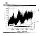
- FIG. 2illustrates a graph plotting the contact resistance values between a test contact and a contact connecting area with a solderable layer including a metal alloy.
- FIG. 3illustrates a graph plotting the contact resistance values between a test contact and a contact connecting area with a solderable layer including a metal.
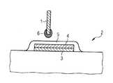
- FIG. 1shows a semiconductor component and a test contact according to an embodiment of the invention.
- the semiconductor component 2includes an external contact area 3 on which a layer of solderable material 4 may be applied.
- the layer of solderable material 4(also called a solderable layer) may include a metal (e.g., tin) or a metal alloy (e.g., tin/lead, tin/lead/silver, bismuth/silver/copper, and/or bismuth/nickel/copper).
- the solderable layer 4may be applied using processes including, but not limited to, galvanic processes.
- galvanic depositionis understood to be both a current-less deposition from a chemical bath and an electrolytic deposition with current in an electrolyte bath.
- Applying the wetting fluid 5 to the external contact area 3prevents contamination of the contact area before this contamination is transferred to the test contact 1 , which would increase the transition resistance values during subsequent contacting cycles of the test contact with external contact areas.
- the presence of the wetting fluid 5produces a very low, relatively constant transition resistance during contact of the test contact 1 with the semiconductor component 2 , even when contact is frequent.
- the fluid 5prevents contamination of the contact surfaces of the semiconductor component 2 (e.g., by oxidation or sulfidation).
- the wetting fluid 5may have a reducing effect, protecting against further oxidation.
- better contact of the base materialis provided since existing oxide layers are interrupted and/or loosened by the fluid 5 .
- test contact 1displaces the fluid and removes it from the contact points between test contact and the external contact area 3 .
- the solvents of the fluidhave dried up, whereas the active substances of the fluid remain on the contact surfaces.
- FIGS. 2 and 3are plotted graphs of the resistance values occurring between the test contact 1 and the external contact area 3 .
- a test contact 1was connected to the external contact area 3 of a pair semiconductor components 2 —one with the fluid layer 5 and one without the fluid layer.
- the external contact area 3 of a first semiconductor component 2was wetted with the fluid 5 before establishing contact with the first test contact 1
- the external contact area 3 of a second semiconductor component 2was not wetted with the fluid 5 before establishing contact with the second test contact 1 .
- the test contacts 1were in each case a pogo pin with a head 6 of hard gold.
- Each test contact 1was brought into contact with external contact areas 3 250,000 times.
- the galvanically applied solderable coating 4was of an alloy including approximately 80 atomic % tin and approximately 20 atomic % lead.
- the measured resistance between the test contact 1 and the external contact area 3 wetted with the fluid 5(plotted line A) remained stable at approximately 0.8 ohms, even when contact is established up to 250,000 times.
- the external contact area 3 that was not wetted with the fluid 5(plotted line B) possesses measured resistance values that vary between 0.08 ohms and 1.7 ohms.
- resistances greater than 0.4 ohmsbegin to occur.
Landscapes
- Physics & Mathematics (AREA)
- General Physics & Mathematics (AREA)
- Measuring Leads Or Probes (AREA)
- Testing Of Individual Semiconductor Devices (AREA)
- Preventing Corrosion Or Incrustation Of Metals (AREA)
Abstract
Description
- This application claims priority under 35 U.S.C. § 119 to German Application No. DE 10 2005 032 142.9, filed 07 Jul. 2005 and entitled “Method for Contacting Semiconductor Components with a Test Contact”, the disclosure of which is hereby incorporated by reference in its entirety.
- The invention relates to a method for contacting semiconductor components with a test contact.
- During the testing of semiconductor components during production, the external contacts of the semiconductor components are brought into contact with test heads of a tester in order to electrically connect the tester to the semiconductor components. As described in U.S. Published Patent Application No. 2005/0140009 to Groeninger (the disclosure of which is incorporated by reference in its entirety), external contact areas are increasingly arranged on the underside of electronic components. These are used for connection with higher-level circuit parts and replace the contact pins previously arranged at the edge in the form of external flat conductors.
- Before an external contact area is connected to the higher-level circuit arrangement or to solder pads, its coated with a layer of solderable material. This layer is formed from metals or metal alloys that are galvanically deposited on the external contact area and, in this process, forms a matte surface with sharp edges. However, such a galvanically deposited layer has a disadvantageous effect on the transition and contact resistance during functional tests of the electronic component. This, in turn, impairs the life of the elastic test contacts, especially since these are contaminated with the layer material of the external contact areas even after a few test cycles. The test contacts must be frequently cleaned or exchanged. The fluctuating transition resistances also impair the yield of the first test sequences (this yield is called the “first pass yield”). Accordingly, these first test sequences must be repeated in order to find out whether the yield losses are caused by faulty components or by large transition resistances. These subsequent tests increase the expenditure and lead to a low production throughput.
- The present invention provides, inter alia, a method wherein the external contact areas and the test contacts are connected in such a manner that the yield during the tests and the production throughput is increased. In particular, a method for contacting external contact areas of a semiconductor component with a test contact is provided. In one embodiment, a coating of solderable material is applied to the external contact areas. The solderable material may include a metal (e.g., tin) or a metal alloy (e.g., tin/lead, tin/lead/silver, bismuth/silver/copper, and/or bismuth/nickel/copper). A wetting fluid is further applied to the external contact areas. The wetting fluid may be a solution containing a binder, an inhibitor, and a lubricant. The binder may include, for example, white mineral oil and/or ethyl acetate. The inhibitor may be an aliphatic hydrocarbon. The lubricant may include, for example, methyl oleate and/or castor oil.
- The substance is generally not applied to the measuring/testing contacts, but is instead used for wetting the terminals of the electronic components. This prevents contamination of the contact areas before this contamination is transferred to the test contact, which would increase the transition resistance values during subsequent contacting cycles of the test contact with external contact areas. As a result, the yield losses are reduced and the first test sequences do not need to be repeated. This, in turn, increases the production throughput. It is of importance, particularly in the case of critical high-frequency components, that the transition resistance values between a test contact and the external contact areas remain low. The measuring accuracy is improved by means of the method according to the invention.
- In one embodiment of the invention, the test contact is a pogo pin. When a pogo pin is mechanically pressed onto the external contact area, cracks in the galvanic coating of the external contact areas are produced. Along these cracks, there can be increased contamination. This contamination is prevented by applying the wetting fluid. As a result, the pogo pins are exposed to less contamination, and the contacts need to be cleaned less frequently. This also increases the life of the pogo pins.
FIG. 1 illustrates a cross sectional view of a semiconductor component according to an embodiment of the invention, showing an external contact area and a test contact.FIG. 2 . illustrates a graph plotting the contact resistance values between a test contact and a contact connecting area with a solderable layer including a metal alloy.FIG. 3 illustrates a graph plotting the contact resistance values between a test contact and a contact connecting area with a solderable layer including a metal.FIG. 1 shows a semiconductor component and a test contact according to an embodiment of the invention. As shown, the semiconductor component2 includes anexternal contact area 3 on which a layer ofsolderable material 4 may be applied. The layer of solderable material4 (also called a solderable layer) may include a metal (e.g., tin) or a metal alloy (e.g., tin/lead, tin/lead/silver, bismuth/silver/copper, and/or bismuth/nickel/copper). Thesolderable layer 4 may be applied using processes including, but not limited to, galvanic processes. In this context, galvanic deposition is understood to be both a current-less deposition from a chemical bath and an electrolytic deposition with current in an electrolyte bath.- The solderable material enables the
external contact areas 3 to be connected directly to corresponding contact areas of a higher-level circuit system of a metal or of a metal alloy that is galvanically applied. By way of specific example, thesolderable layer 4 may include a tin/lead/silver alloy, wherein tin is contained with approximately 50 to 70 atomic %, lead with approximately 30 to 40 atomic %, and silver with approximately 1 to 10 atomic %. The metal alloy may further include a bismuth/silver/copper alloy having approximately 50 to 80 atomic % bismuth, 5 to 40 atomic % silver, and 0.5 to 15 atomic % copper. By way of further example, an alloy based on bismuth/nickel/copper may have approximately 50 to 85 atomic % bismuth, 15 to 45 atomic % copper, and 0.5 to 5 atomic % nickel. - Then, before establishing contact between the
external contact area 3 and thetest contact 1, awetting fluid 5 may applied over theexternal contact area 3 such that it encloses thesolderable layer 4. Establishing contact is here understood to be the mechanical contacting of the test contact1 (e.g., by means of its test head) to the semiconductor component2. Thewetting fluid 5 may be a solution containing a binder (also called a coupling means or solvent), an inhibitor, and a lubricant. The binder may include, but is not limited to, white mineral oil and/or ethyl acetate. The inhibitor may be an aliphatic hydrocarbon. The lubricant may include, for example, methyl oleate and/or castor oil. Once thefluid 5 wets thecontact area 3, thehead 6 of thetest contact 1 is conducted from the top onto theexternal contact area 3. By way of specific example, thetest contact 1 may include a pogo pin with ahead 6 formed of hard gold. - Applying the
wetting fluid 5 to theexternal contact area 3 prevents contamination of the contact area before this contamination is transferred to thetest contact 1, which would increase the transition resistance values during subsequent contacting cycles of the test contact with external contact areas. Thus, the presence of thewetting fluid 5 produces a very low, relatively constant transition resistance during contact of thetest contact 1 with the semiconductor component2, even when contact is frequent. Thefluid 5 prevents contamination of the contact surfaces of the semiconductor component2 (e.g., by oxidation or sulfidation). The wettingfluid 5 may have a reducing effect, protecting against further oxidation. Thus, better contact of the base material is provided since existing oxide layers are interrupted and/or loosened by thefluid 5. - In addition, if the wetting
fluid 5 is dried before contact is established, there is no risk that thetest contact 1 displaces the fluid and removes it from the contact points between test contact and theexternal contact area 3. During the drying, the solvents of the fluid have dried up, whereas the active substances of the fluid remain on the contact surfaces. FIGS. 2 and 3 are plotted graphs of the resistance values occurring between thetest contact 1 and theexternal contact area 3. In one experiment, atest contact 1 was connected to theexternal contact area 3 of a pair semiconductor components2—one with thefluid layer 5 and one without the fluid layer. Specifically, theexternal contact area 3 of a first semiconductor component2 was wetted with thefluid 5 before establishing contact with thefirst test contact 1, while theexternal contact area 3 of a second semiconductor component2 was not wetted with thefluid 5 before establishing contact with thesecond test contact 1. Thetest contacts 1 were in each case a pogo pin with ahead 6 of hard gold. Eachtest contact 1 was brought into contact withexternal contact areas 3 250,000 times. In this particular embodiment, the galvanically appliedsolderable coating 4 was of an alloy including approximately 80 atomic % tin and approximately 20 atomic % lead.- As shown in
FIG. 2 , the measured resistance between thetest contact 1 and theexternal contact area 3 wetted with the fluid5 (plotted line A) remained stable at approximately 0.8 ohms, even when contact is established up to 250,000 times. In contrast, theexternal contact area 3 that was not wetted with the fluid5 (plotted line B) possesses measured resistance values that vary between 0.08 ohms and 1.7 ohms. In addition, after only 50,000 contact cycles, resistances greater than 0.4 ohms begin to occur. - In a second experiment, the galvanically applied
alloy coating 4 was replaced with a tin coating. Referring toFIG. 3 , when theexternal contact area 3 was wetted with thefluid 5, consistent resistance readings of approximately 0.05 ohms are achieved (plotted line A). In contrast, the resistance of the semiconductor component2 without the fluid5 (plotted line B) possesses resistance values varying between about 0.5 ohms to about 0.45 ohms. Thus, it can be seen the presence of the wettingfluid 5 produces a very low, relatively constant transition resistance during contact of thetest contact 1 with the semiconductor component2, even when contact is frequent. - List of reference designations:
- 1 Test contact
- 2 Semiconductor component
- 3 External contact area
- 4 Coating
- 5 Fluid
- 6 Gold head
Claims (17)
Applications Claiming Priority (2)
| Application Number | Priority Date | Filing Date | Title |
|---|---|---|---|
| DE102005032142.9ADE102005032142B4 (en) | 2005-07-07 | 2005-07-07 | A method of contacting semiconductor devices with a test contact |
| DE102005032.142.9 | 2005-07-07 |
Publications (2)
| Publication Number | Publication Date |
|---|---|
| US20070007514A1true US20070007514A1 (en) | 2007-01-11 |
| US7642104B2 US7642104B2 (en) | 2010-01-05 |
Family
ID=37563405
Family Applications (1)
| Application Number | Title | Priority Date | Filing Date |
|---|---|---|---|
| US11/456,122Expired - Fee RelatedUS7642104B2 (en) | 2005-07-07 | 2006-07-07 | Method for contacting semiconductor components with a test contact |
Country Status (2)
| Country | Link |
|---|---|
| US (1) | US7642104B2 (en) |
| DE (1) | DE102005032142B4 (en) |
Cited By (1)
| Publication number | Priority date | Publication date | Assignee | Title |
|---|---|---|---|---|
| US20150083796A1 (en)* | 2013-09-24 | 2015-03-26 | Center For Integrated Smart Sensors Foundation | Nfc or rfid based sensor measurement device and measuring method using the same |
Citations (9)
| Publication number | Priority date | Publication date | Assignee | Title |
|---|---|---|---|---|
| US3632509A (en)* | 1969-06-11 | 1972-01-04 | Matsushita Electric Industrial Co Ltd | Electric contact grease |
| US4696832A (en)* | 1985-06-11 | 1987-09-29 | D. W. Electrochemicals Ltd. | Contact stabilization coating material for electrical contact surfaces and method |
| US5661042A (en)* | 1995-08-28 | 1997-08-26 | Motorola, Inc. | Process for electrically connecting electrical devices using a conductive anisotropic material |
| US6162652A (en)* | 1997-12-31 | 2000-12-19 | Intel Corporation | Process for sort testing C4 bumped wafers |
| US20020195746A1 (en)* | 2001-06-22 | 2002-12-26 | Hull Charles W. | Recoating system for using high viscosity build materials in solid freeform fabrication |
| US6528125B1 (en)* | 1999-06-08 | 2003-03-04 | Itt Manufacturing Enterprises, Inc. | Corrosion resistant powder coated metal tube and process for making the same |
| US20050140009A1 (en)* | 2002-06-17 | 2005-06-30 | Horst Groeninger | Method and apparatus for the production of an electronic component with external contact areas |
| US20050205865A1 (en)* | 2004-03-19 | 2005-09-22 | Hang-Dony Kuan | IC testing apparatus and methods |
| US7319341B1 (en)* | 2003-08-28 | 2008-01-15 | Altera Corporation | Method of maintaining signal integrity across a capacitive coupled solder bump |
Family Cites Families (4)
| Publication number | Priority date | Publication date | Assignee | Title |
|---|---|---|---|---|
| JP3112744B2 (en) | 1991-09-12 | 2000-11-27 | タムラ化研株式会社 | Surface protective agent for printed wiring boards |
| JPH08338852A (en)* | 1995-06-13 | 1996-12-24 | Sony Corp | Test probe |
| WO2003107413A2 (en)* | 2002-06-17 | 2003-12-24 | Infineon Technologies Ag | Method and device for producing an electronic component having external contact surfaces |
| AT412094B (en) | 2003-05-13 | 2004-09-27 | Austria Tech & System Tech | Blank for the production of printed circuit boards, comprises an acid-resistant protective film of at least two layers that are chemically bonded to each other and to the metallic surface of the blank |
- 2005
- 2005-07-07DEDE102005032142.9Apatent/DE102005032142B4/ennot_activeExpired - Fee Related
- 2006
- 2006-07-07USUS11/456,122patent/US7642104B2/ennot_activeExpired - Fee Related
Patent Citations (9)
| Publication number | Priority date | Publication date | Assignee | Title |
|---|---|---|---|---|
| US3632509A (en)* | 1969-06-11 | 1972-01-04 | Matsushita Electric Industrial Co Ltd | Electric contact grease |
| US4696832A (en)* | 1985-06-11 | 1987-09-29 | D. W. Electrochemicals Ltd. | Contact stabilization coating material for electrical contact surfaces and method |
| US5661042A (en)* | 1995-08-28 | 1997-08-26 | Motorola, Inc. | Process for electrically connecting electrical devices using a conductive anisotropic material |
| US6162652A (en)* | 1997-12-31 | 2000-12-19 | Intel Corporation | Process for sort testing C4 bumped wafers |
| US6528125B1 (en)* | 1999-06-08 | 2003-03-04 | Itt Manufacturing Enterprises, Inc. | Corrosion resistant powder coated metal tube and process for making the same |
| US20020195746A1 (en)* | 2001-06-22 | 2002-12-26 | Hull Charles W. | Recoating system for using high viscosity build materials in solid freeform fabrication |
| US20050140009A1 (en)* | 2002-06-17 | 2005-06-30 | Horst Groeninger | Method and apparatus for the production of an electronic component with external contact areas |
| US7319341B1 (en)* | 2003-08-28 | 2008-01-15 | Altera Corporation | Method of maintaining signal integrity across a capacitive coupled solder bump |
| US20050205865A1 (en)* | 2004-03-19 | 2005-09-22 | Hang-Dony Kuan | IC testing apparatus and methods |
Cited By (1)
| Publication number | Priority date | Publication date | Assignee | Title |
|---|---|---|---|---|
| US20150083796A1 (en)* | 2013-09-24 | 2015-03-26 | Center For Integrated Smart Sensors Foundation | Nfc or rfid based sensor measurement device and measuring method using the same |
Also Published As
| Publication number | Publication date |
|---|---|
| US7642104B2 (en) | 2010-01-05 |
| DE102005032142A1 (en) | 2007-01-18 |
| DE102005032142B4 (en) | 2014-10-09 |
Similar Documents
| Publication | Publication Date | Title |
|---|---|---|
| Lu et al. | Mechanisms underlying the unstable contact resistance of conductive adhesives | |
| JP6112792B2 (en) | Method of using electrical contact and electrical contact | |
| KR101427506B1 (en) | Contact probe | |
| US20040041241A1 (en) | Packaged semiconductor with coated leads and method therefore | |
| JP6647075B2 (en) | Alloy materials, contact probes and connection terminals | |
| US20090243640A1 (en) | Conductive contact pin and semiconductor testing equipment | |
| US20200354849A1 (en) | Metallic terminal and manufacturing method thereof | |
| US5957736A (en) | Electronic part | |
| Hanss et al. | Process development and reliability of sintered high power chip size packages and flip chip LEDs | |
| KR100825231B1 (en) | Method for manufacturing probe needle used in probe card and probe needle | |
| US7642104B2 (en) | Method for contacting semiconductor components with a test contact | |
| CN102055101B (en) | Electrical connector terminal | |
| Ambat et al. | A review of Corrosion and environmental effects on electronics | |
| Dumoulin et al. | Metal migrations outside the package during accelerated life tests | |
| CA2105493C (en) | Method and apparatus for assessing and restoring solderability | |
| JP5503477B2 (en) | Contact probe and electronic circuit test apparatus using the same | |
| Zhang et al. | Research on the contact resistance, reliability, and degradation mechanisms of anisotropically conductive film interconnection for flip-chip-on-flex applications | |
| JP2009272424A (en) | Printed circuit board and method of manufacturing the same | |
| US7132840B2 (en) | Method of electrical testing | |
| KR20090103738A (en) | Conductive contactor and apparatus for inspecting a semiconductor | |
| JPH05203670A (en) | Contact probe | |
| TWI420753B (en) | Electrical connector contact | |
| JPH09232057A (en) | Ic socket | |
| JP2007256078A (en) | Multilayer probe pins and probe cards | |
| KR100840444B1 (en) | Electronic parts |
Legal Events
| Date | Code | Title | Description |
|---|---|---|---|
| AS | Assignment | Owner name:INFINEON TECHNOLOGIES AG, GERMANY Free format text:ASSIGNMENT OF ASSIGNORS INTEREST;ASSIGNOR:GROENINGER, HORST;REEL/FRAME:018216/0001 Effective date:20060809 | |
| FEPP | Fee payment procedure | Free format text:PAYER NUMBER DE-ASSIGNED (ORIGINAL EVENT CODE: RMPN); ENTITY STATUS OF PATENT OWNER: LARGE ENTITY Free format text:PAYOR NUMBER ASSIGNED (ORIGINAL EVENT CODE: ASPN); ENTITY STATUS OF PATENT OWNER: LARGE ENTITY | |
| STCF | Information on status: patent grant | Free format text:PATENTED CASE | |
| FPAY | Fee payment | Year of fee payment:4 | |
| FPAY | Fee payment | Year of fee payment:8 | |
| FEPP | Fee payment procedure | Free format text:MAINTENANCE FEE REMINDER MAILED (ORIGINAL EVENT CODE: REM.); ENTITY STATUS OF PATENT OWNER: LARGE ENTITY | |
| LAPS | Lapse for failure to pay maintenance fees | Free format text:PATENT EXPIRED FOR FAILURE TO PAY MAINTENANCE FEES (ORIGINAL EVENT CODE: EXP.); ENTITY STATUS OF PATENT OWNER: LARGE ENTITY | |
| STCH | Information on status: patent discontinuation | Free format text:PATENT EXPIRED DUE TO NONPAYMENT OF MAINTENANCE FEES UNDER 37 CFR 1.362 | |
| FP | Lapsed due to failure to pay maintenance fee | Effective date:20220105 |