US20070002603A1 - Memory cell with high-K antifuse for reverse bias programming - Google Patents
Memory cell with high-K antifuse for reverse bias programmingDownload PDFInfo
- Publication number
- US20070002603A1 US20070002603A1US11/174,240US17424005AUS2007002603A1US 20070002603 A1US20070002603 A1US 20070002603A1US 17424005 AUS17424005 AUS 17424005AUS 2007002603 A1US2007002603 A1US 2007002603A1
- Authority
- US
- United States
- Prior art keywords
- diode
- integrated circuit
- antifuse
- memory cell
- memory
- Prior art date
- Legal status (The legal status is an assumption and is not a legal conclusion. Google has not performed a legal analysis and makes no representation as to the accuracy of the status listed.)
- Granted
Links
Images


Classifications
- G—PHYSICS
- G11—INFORMATION STORAGE
- G11C—STATIC STORES
- G11C16/00—Erasable programmable read-only memories
- G11C16/02—Erasable programmable read-only memories electrically programmable
- G11C16/06—Auxiliary circuits, e.g. for writing into memory
- G11C16/10—Programming or data input circuits
- G—PHYSICS
- G11—INFORMATION STORAGE
- G11C—STATIC STORES
- G11C17/00—Read-only memories programmable only once; Semi-permanent stores, e.g. manually-replaceable information cards
- G11C17/14—Read-only memories programmable only once; Semi-permanent stores, e.g. manually-replaceable information cards in which contents are determined by selectively establishing, breaking or modifying connecting links by permanently altering the state of coupling elements, e.g. PROM
- G11C17/16—Read-only memories programmable only once; Semi-permanent stores, e.g. manually-replaceable information cards in which contents are determined by selectively establishing, breaking or modifying connecting links by permanently altering the state of coupling elements, e.g. PROM using electrically-fusible links
- G—PHYSICS
- G11—INFORMATION STORAGE
- G11C—STATIC STORES
- G11C11/00—Digital stores characterised by the use of particular electric or magnetic storage elements; Storage elements therefor
- G11C11/56—Digital stores characterised by the use of particular electric or magnetic storage elements; Storage elements therefor using storage elements with more than two stable states represented by steps, e.g. of voltage, current, phase, frequency
- G11C11/5692—Digital stores characterised by the use of particular electric or magnetic storage elements; Storage elements therefor using storage elements with more than two stable states represented by steps, e.g. of voltage, current, phase, frequency read-only digital stores using storage elements with more than two stable states
- G—PHYSICS
- G11—INFORMATION STORAGE
- G11C—STATIC STORES
- G11C13/00—Digital stores characterised by the use of storage elements not covered by groups G11C11/00, G11C23/00, or G11C25/00
- G11C13/0002—Digital stores characterised by the use of storage elements not covered by groups G11C11/00, G11C23/00, or G11C25/00 using resistive RAM [RRAM] elements
- G11C13/0021—Auxiliary circuits
- G11C13/0069—Writing or programming circuits or methods
- G—PHYSICS
- G11—INFORMATION STORAGE
- G11C—STATIC STORES
- G11C17/00—Read-only memories programmable only once; Semi-permanent stores, e.g. manually-replaceable information cards
- G11C17/14—Read-only memories programmable only once; Semi-permanent stores, e.g. manually-replaceable information cards in which contents are determined by selectively establishing, breaking or modifying connecting links by permanently altering the state of coupling elements, e.g. PROM
- G11C17/16—Read-only memories programmable only once; Semi-permanent stores, e.g. manually-replaceable information cards in which contents are determined by selectively establishing, breaking or modifying connecting links by permanently altering the state of coupling elements, e.g. PROM using electrically-fusible links
- G11C17/165—Memory cells which are electrically programmed to cause a change in resistance, e.g. to permit multiple resistance steps to be programmed rather than conduct to or from non-conduct change of fuses and antifuses
- G—PHYSICS
- G11—INFORMATION STORAGE
- G11C—STATIC STORES
- G11C29/00—Checking stores for correct operation ; Subsequent repair; Testing stores during standby or offline operation
- G11C29/04—Detection or location of defective memory elements, e.g. cell constructio details, timing of test signals
- G—PHYSICS
- G11—INFORMATION STORAGE
- G11C—STATIC STORES
- G11C13/00—Digital stores characterised by the use of storage elements not covered by groups G11C11/00, G11C23/00, or G11C25/00
- G11C13/0002—Digital stores characterised by the use of storage elements not covered by groups G11C11/00, G11C23/00, or G11C25/00 using resistive RAM [RRAM] elements
- G11C13/0021—Auxiliary circuits
- G11C13/0069—Writing or programming circuits or methods
- G11C2013/0073—Write using bi-directional cell biasing
- G—PHYSICS
- G11—INFORMATION STORAGE
- G11C—STATIC STORES
- G11C13/00—Digital stores characterised by the use of storage elements not covered by groups G11C11/00, G11C23/00, or G11C25/00
- G11C13/0002—Digital stores characterised by the use of storage elements not covered by groups G11C11/00, G11C23/00, or G11C25/00 using resistive RAM [RRAM] elements
- G11C13/0021—Auxiliary circuits
- G11C13/0069—Writing or programming circuits or methods
- G11C2013/009—Write using potential difference applied between cell electrodes
- G—PHYSICS
- G11—INFORMATION STORAGE
- G11C—STATIC STORES
- G11C2213/00—Indexing scheme relating to G11C13/00 for features not covered by this group
- G11C2213/70—Resistive array aspects
- G11C2213/71—Three dimensional array
- G—PHYSICS
- G11—INFORMATION STORAGE
- G11C—STATIC STORES
- G11C2213/00—Indexing scheme relating to G11C13/00 for features not covered by this group
- G11C2213/70—Resistive array aspects
- G11C2213/72—Array wherein the access device being a diode
Definitions
- the present applicationis related to a first co-pending application filed coincidently herewith under Attorney Docket Number MA-153, naming N. Johan Knall as sole inventor, and entitled “REVERSE-BIAS METHOD FOR WRITING MEMORY CELLS IN A MEMORY ARRAY,” and a second co-pending application filed coincidently herewith under Attorney Docket Number MA-155, naming inventor Xiaoyu Yang et al., and entitled “MEMORY WITH HIGH DIELECTRIC CONSTANT ANTIFUSES AND METHOD FOR USING AT LOW VOLTAGE,” which are each incorporated herein by reference in their entirety for all purposes.
- the present inventionrelates to memory devices, and more particularly to memory cells equipped with antifuses.
- An integrated circuit and associated method of programmingare provided.
- Such integrated circuitincludes a memory cell with a diode and an antifuse in communication with the diode.
- the antifuseis constructed to include a high-K dielectric material with a K greater than 3.9.
- the memory cellis programmed utilizing a programming pulse that reverse biases the diode thereof.
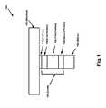
- FIG. 1is a cross-sectional view showing a portion of an integrated circuit including a memory cell, according to one embodiment.
- FIG. 2illustrates a method for programming an array of memory cells, in accordance with another embodiment.
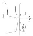
- FIG. 3is a graph showing a current vs. voltage relationship for a diode, in accordance with another embodiment.
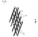
- FIG. 4shows a three-dimensional array of memory cells, in accordance with another embodiment.
- FIG. 1is a cross-sectional view showing a portion of an integrated circuit including a memory cell 100 , according to one embodiment. While only a portion of such integrated circuit is shown, it should be understood that a multiplicity of memory cells 100 may be interconnected in an array that may span in two directions. Further, while only one memory cell 100 will initially be described in the context of only one level of the memory cells 100 , it should further be noted that, in some optional embodiments, a plurality of levels of the memory cells 100 may be vertically disposed to form a three-dimensional array of memory cells 100 . More information regarding such a three-dimensional array embodiment will be set forth hereinafter in greater detail during reference to FIG. 4 .
- the memory cell 100is equipped with a diode 105 and an antifuse 110 in communication with the diode 105 .
- the diode 105 and antifuse 110are positioned between a word line 102 and a bit line 104 .
- the antifuse 110may be a dielectric layer between diode portions such that the diode 105 is formed after the antifuse 110 is ruptured. More information regarding possible antifuse constructions and related operation will be set forth hereinafter in greater detail.
- the word line 102 and bit line 104may take the form of rails for interconnecting a plurality of the memory cells 100 .
- the diode 105may include a first portion 106 having a first heavily doped semiconductor material with a first conductivity type (e.g. P-type, N-type) and at least one other portion having an intrinsic semiconductor material or a doped semiconductor material with a second conductivity type (e.g. N-type, P-type) opposite the first conductivity type.
- the antifuse 110may be in contact with the first portion 106 of the diode 105 (as shown), and/or in contact with the at least one other portion of the diode 105 .
- a second portion 108 of the diode 105may be provided with a heavily doped semiconductor material having the second conductivity type. Further, the diode 105 may also include a third portion 109 including an intrinsic or a lightly doped semiconductor material. While any material may be utilized for construction of the diode 105 , the diode 105 may, in one embodiment, be constructed utilizing a polycrystalline semiconductor material, such as polycrystalline silicon. Of course, any material capable of providing the diode 105 may be utilized.
- the first portion 106 of the diode 105may be disposed vertically above the second portion 108 of the diode 105 .
- the third portion 109 of the diode 105may be disposed vertically between the first portion 106 of the diode 105 and the second portion 108 of the diode 105 .
- the various portions of the diode 105may be constructed as a rail, pillars, and/or any other desired configuration.
- the antifuse 110may, in various embodiments, be disposed vertically below the second portion 108 of the diode 105 , and/or vertically between the first portion 106 of the diode 105 and the second portion 108 of the diode 105 .
- the antifuse 110may be disposed vertically between the second portion 108 of the diode 105 and the third portion 109 of the diode 105 , and/or between the first portion 106 of the diode 105 and the third portion 109 of the diode 105 .
- the antifuse 110may be disposed between a plus concentration of one conductivity type and a minus concentration of another conductivity type (e.g. between P+ and N ⁇ conductivity types or between N+ and P ⁇ conductivity types).
- each memory cell 100is disposed between the word line 102 and bit line 104 in such a manner that an individual memory cell 100 may be programmed by applying a programming voltage between an associated word line 102 and bit line 104 .
- the antifuse 110may provide a barrier to voltage-induced current when the memory cell 100 is in an un-programmed state. When a sufficient programming voltage is applied to the memory cell 100 , the antifuse 110 experiences dielectric breakdown, and a permanent conductive path through the antifuse 110 is formed. Thereafter, the diode 105 is free to serve as a one-way valve, allowing current flow in one direction only.
- the memory cell 100is subjected to a programming pulse that reverse biases the diode 105 thereof. More information regarding such reverse bias programming is set forth in greater detail hereinafter as well as in a co-pending application filed coincidently herewith under Attorney Docket Number MA-153, naming N. Johan Knall as sole inventor, and entitled “REVERSE-BIAS METHOD FOR WRITING MEMORY CELLS IN A MEMORY ARRAY,” hereinafter referred to as “Co-Pending Application,” which was previously incorporated.
- the antifuse 110includes a high-K dielectric material with a K greater than 3.9.
- any high-K dielectric materialmay be employed in the construction of the antifuse 110 .
- the high-K dielectric materialmay be titanium oxide, tantalum oxide, hafnium oxide, and/or aluminum oxide. Such list is not exhaustive and should not be construed as limiting in any manner, as any high-K dielectric material with a K greater than 3.9 may be employed.
- additional examples of high-K dielectric materialmay be found with reference to McPherson et al., “Proposed Universal Relationship Between Dielectric Breakdown and Dielectric Constant,” IEEE International Electron Devices Meeting, 2002, pp. 26.6.1-4, which is incorporated herein by reference in its entirety for all purposes.
- memory cellsmay be programmed utilizing reverse bias programming techniques and lower-K dielectric antifuses, such as silicon dioxide.
- the aforementioned reverse biasingrequires a higher bias voltage.
- the amount of current provided at a predetermined voltageis less for reverse biasing with respect to forward biasing.
- the lower-K dielectric antifuserequires a greater negative voltage to provide the current necessary to rupture the same.
- Such negative voltageis so high that full reverse breakdown of the diode may occur during the programming.
- Such breakdownis a condition where the amount of current through the diode rises dramatically as a function of voltage (this is undesirable for numerous reasons including power consumption).
- the elevated reverse bias voltagewhen used in combination with lower-K dielectric antifuses, has a potential of heating up and/or damaging the associated diode when the antifuse ruptures, as well as consuming large quantities of power.
- an antifuse including a high-K dielectric material with a K greater than 3 . 9in the context of the memory cell of FIG. 1 , a lower programming voltage is required.
- the high-K dielectric antifuseexhibits a lower current density at the point of rupture, with respect to lower-K dielectric counterparts.
- the antifuseis ruptured in reverse at a voltage below the reverse breakdown voltage of the diode.
- the high-K dielectric antifusemay provide the foregoing benefits, it may also exhibit additional undesired leakage during read operations.
- This leakagemay optionally be addressed by thickening the high-K dielectric antifuse to the point that the voltage at which rupture occurs is similar to lower-K dielectric counterparts. By this design, leakage may be less than that exhibited by lower-K dielectric antifuses and the same voltages can be used by associated drivers and sense amplifiers.
- the thicker high-K dielectric antifusedoes rupture, the current density is much less than that of lower-K dielectric antifuses, thus providing the foregoing benefits. It should be noted that with a higher K, a greater margin is provided from reverse breakdown of the diode, as will become more apparent during reference to FIG. 3 .
- Such embodimentfurther facilitates lower-power, multiple bit/level programming, which will be set forth hereinafter in greater detail.
- Different diode structuresmay be employed.
- P+N diode configurationsi.e. first portion 106 including a P+ conductivity type, and second portion 108 including an N conductivity type
- additional diode structuressuch as N+P (i.e. first portion 106 including an N+ conductivity type, and second portion 108 including a P conductivity type) may further be employed.
- FIG. 2illustrates a method 200 for programming an array of memory cells, in accordance with another embodiment.
- the method 200may be utilized to program memory cells similar to the memory cell 100 of FIG. 1 .
- the method 200may be carried out to program any desired memory cell(s).
- various operationsare set forth in the context of the present method 200 , various operations may be omitted, and/or additional unillustrated operations may, of course, be employed as desired.
- a programming eventis started for programming at least one memory cell (e.g. memory cell 100 of FIG. 1 ) including a diode and an antifuse in communication with the diode.
- a programming voltageis applied to at least one memory cell for reverse biasing the diode of the memory cell.
- the programming voltagemay be applied to a plurality of memory cells simultaneously. Note bit 1 , bit 2 , and bit N of FIG. 2 .
- bit 1 , bit 2 , and bit N of FIG. 2may be programmed at a time.
- the number of memory cells that are programmed over timemay be increased.
- simultaneous memory cell programmingmay be facilitated by virtue of the fact that the high-K dielectric antifuse may possibly require less current.
- the aforementioned programming pulsemay be slightly longer temporally, but on a whole, far more memory cells may be programmed, such that a pulse length may rise by a factor of 2-10 ⁇ (for example), but the number of memory cells to be programmed may rise by a factor of 10 to 10,000 (for example).
- a first soaking pulsemay be applied to a first memory cell (e.g. bit 1 ) under a first soak condition, which forward biases the diode of the memory cell.
- a second soaking pulsemay be applied to a second memory cell (e.g. bit 2 ) under a second soak condition, which also forward biases the diode of such memory cell.
- additional soaking pulsesmay be applied to additional memory cells (e.g. bit N), for reasons that will soon become apparent.
- the soaking pulseis an option and may be applied to the appropriate memory cells one at a time in the foregoing manner, such that multiple levels are set for each bit.
- the soaking pulsemay not be necessary.
- the required current flowis high enough when forward biasing the diode, a reduced number of bits may be simultaneously programmed, due to power limitations.
- different soaking pulsesmay be applied to the memory cells, which results in the diode of each memory cell being capable of exhibiting one of a plurality of different resistances when turned on.
- the diodemay be equipped with a lower resistance by forcing a larger current therethrough using the soaking pulse. This phenomenon results from a filament formed through the antifuse becoming larger as it is heated with additional current.
- a “0” statemay exhibit 10 megaOhms across the cell
- a “1” statemay exhibit 1000 ohms
- a “ 2 ” statemay exhibit 500 ohms
- a “3” statemay exhibit 100 ohms.
- these resistance levelsare merely illustrative in nature and should not be construed as limiting in any manner.
- the on current of each memory cellmay be set by soaking at a high forward bias.
- the level of the on bitmay be set by choosing a soak condition that gives a different on condition for one memory cell with respect to another.
- a first memory cellmay be set, or programmed, by a forward voltage of 3V and may pass 500 nA at 2V (due to the presence of a first resistance).
- a second memory cellmay be set with a 5V forward bias, which may result in the second memory cell passing more than 1 uA at 2V (due to the presence of a second resistance).
- FIG. 3is a graph 300 showing a current vs. voltage relationship for a diode, in accordance with another embodiment.
- the current vs. voltage relationship shown in the graph 300may reflect the operation of the memory cell 100 of FIG. 1 .
- an additional buffer 302or margin, is provided between voltage ⁇ V R at which the antifuse ruptures, and the voltage ⁇ V B where the diode is damaged due to reverse bias breakdown. To this end, damage to the diode is avoided during programming, while affording the various optional benefits discussed previously.
- the current vs. voltage relationship of the programmed memory celldiffers from that of an un-programmed memory cell, as shown.
- both a dielectric strength and a current density at ruptureare decreased as a function of an increase in the dielectric constant of the antifuse.
- the diode and antifuseact like two series resistors before and after programming. If the diode is forward biased, it exhibits a low resistance such that most of the voltage is dropped across the antifuse. In reverse bias, the diode has a high resistance. In order for a programming field to be formed across the antifuse when reverse biasing, the antifuse should exhibit a higher resistance with respect to the reverse-biased diode. This condition needs to exist while the reverse bias level is still well below the reverse bias breakdown voltage (see buffer 302 ). This may be necessary to prevent the diode from actually breaking down in reverse, which may result in damage to the diode.
- FIG. 4shows a three-dimensional array 400 of memory cells, in accordance with another embodiment.
- the memory cell array 400may include more than one level of the word lines 402 and/or more than one level of the bit lines 404 with memory cells 406 (e.g. diode 105 and antifuse 110 of the memory cell 100 of FIG. 1 ) formed therebetween.
- a “level” of the three-dimensional array embodimentincludes a plurality of word lines 402 , a plurality of bit lines 404 , and/or a plurality of memory cells 406 substantially positioned in a common approximate plane.
- the level(s) of bit lines 404 and/or level(s) of word lines 402may be monolithically formed above a substrate in the form of a monolithic three dimensional memory array. While the substrate may be formed of any desired material, the substrate may, in one embodiment, include monocrystalline silicon.
- a monolithic three-dimensional memory arrayis one in which multiple memory levels are formed above a single substrate, such as a wafer, with no intervening substrates.
- the layers forming one memory levelare deposited or grown directly over the layers of an existing level or levels.
- stacked memorieshave been constructed by forming memory levels on separate substrates and adhering the memory levels atop each other, as in Leedy, U.S. Pat. No. 5,915,167, “Three dimensional structure memory.”
- the substratesmay be thinned or removed from the memory levels before bonding, but as the memory levels are initially formed over separate substrates, such memories are not true monolithic three-dimensional memory arrays.
- a substrate on which the memory cells are constructedmay include supporting circuitry already formed in a single crystal wafer, where the substrate is capped by a planarized silicon dioxide layer.
- a planarized silicon dioxide layerthere may be openings formed in this oxide layer to accommodate the formation of electrical connections between a memory level(s) and the aforementioned circuitry therebelow.
- a layer of tungsten (W)may be formed over the wafer with or without an underlying adhesion-promoting layer such as Ti/TiN.
- a barrier metal layersuch as TiN may be deposited to prevent formation of WSi during the subsequent deposition of first an N+ doped silicon layer and then, in the same operation, a layer of N ⁇ silicon.
- This stack of layersmay then be patterned into rails using a photoresist mask and plasma-assisted dry etching.
- a silicon dioxide layermay be deposited such that it fills the gaps between the rails. This oxide layer may then be chemical-mechanically polished to expose the silicon at the top of the rail.
- the waferis thereafter implanted with p-type dopant to form a thin layer in the top of the N ⁇ silicon. An antifuse is then either deposited or grown on this surface.
Landscapes
- Engineering & Computer Science (AREA)
- Computer Hardware Design (AREA)
- Semiconductor Memories (AREA)
- Design And Manufacture Of Integrated Circuits (AREA)
- Read Only Memory (AREA)
Abstract
Description
- The present application is related to a first co-pending application filed coincidently herewith under Attorney Docket Number MA-153, naming N. Johan Knall as sole inventor, and entitled “REVERSE-BIAS METHOD FOR WRITING MEMORY CELLS IN A MEMORY ARRAY,” and a second co-pending application filed coincidently herewith under Attorney Docket Number MA-155, naming inventor Xiaoyu Yang et al., and entitled “MEMORY WITH HIGH DIELECTRIC CONSTANT ANTIFUSES AND METHOD FOR USING AT LOW VOLTAGE,” which are each incorporated herein by reference in their entirety for all purposes.
- The present invention relates to memory devices, and more particularly to memory cells equipped with antifuses.
- An integrated circuit and associated method of programming are provided. Such integrated circuit includes a memory cell with a diode and an antifuse in communication with the diode. The antifuse is constructed to include a high-K dielectric material with a K greater than 3.9. Further, the memory cell is programmed utilizing a programming pulse that reverse biases the diode thereof.
FIG. 1 is a cross-sectional view showing a portion of an integrated circuit including a memory cell, according to one embodiment.FIG. 2 illustrates a method for programming an array of memory cells, in accordance with another embodiment.FIG. 3 is a graph showing a current vs. voltage relationship for a diode, in accordance with another embodiment.FIG. 4 shows a three-dimensional array of memory cells, in accordance with another embodiment.FIG. 1 is a cross-sectional view showing a portion of an integrated circuit including amemory cell 100, according to one embodiment. While only a portion of such integrated circuit is shown, it should be understood that a multiplicity ofmemory cells 100 may be interconnected in an array that may span in two directions. Further, while only onememory cell 100 will initially be described in the context of only one level of thememory cells 100, it should further be noted that, in some optional embodiments, a plurality of levels of thememory cells 100 may be vertically disposed to form a three-dimensional array ofmemory cells 100. More information regarding such a three-dimensional array embodiment will be set forth hereinafter in greater detail during reference toFIG. 4 .- As shown in
FIG. 1 , thememory cell 100 is equipped with adiode 105 and an antifuse110 in communication with thediode 105. Thediode 105 and antifuse110 are positioned between aword line 102 and abit line 104. In one embodiment, the antifuse110 may be a dielectric layer between diode portions such that thediode 105 is formed after the antifuse110 is ruptured. More information regarding possible antifuse constructions and related operation will be set forth hereinafter in greater detail. As an option, theword line 102 andbit line 104 may take the form of rails for interconnecting a plurality of thememory cells 100. - Generally, the
diode 105 may include a first portion106 having a first heavily doped semiconductor material with a first conductivity type (e.g. P-type, N-type) and at least one other portion having an intrinsic semiconductor material or a doped semiconductor material with a second conductivity type (e.g. N-type, P-type) opposite the first conductivity type. In various embodiments, the antifuse110 may be in contact with the first portion106 of the diode105 (as shown), and/or in contact with the at least one other portion of thediode 105. - With respect to the at least one other portion of the
diode 105 shown inFIG. 1 , asecond portion 108 of thediode 105 may be provided with a heavily doped semiconductor material having the second conductivity type. Further, thediode 105 may also include athird portion 109 including an intrinsic or a lightly doped semiconductor material. While any material may be utilized for construction of thediode 105, thediode 105 may, in one embodiment, be constructed utilizing a polycrystalline semiconductor material, such as polycrystalline silicon. Of course, any material capable of providing thediode 105 may be utilized. - As further shown, the first portion106 of the
diode 105 may be disposed vertically above thesecond portion 108 of thediode 105. Also, thethird portion 109 of thediode 105 may be disposed vertically between the first portion106 of thediode 105 and thesecond portion 108 of thediode 105. Whereas one configuration is shown inFIG. 1 , it should be noted that the various portions of thediode 105 may be constructed as a rail, pillars, and/or any other desired configuration. - For example, more information regarding an exemplary pillar structure and optional fabrication methods may be found with reference to U.S. Pat. No. 6,034,882, issued Mar. 7, 2000, which is incorporated herein by reference in its entirety for all purposes. Further, more information regarding a possible rail structure may be found with reference to U.S. Pat. No. 6,420,215, issued Jul. 16, 2002, which is incorporated herein by reference in its entirety for all purposes. Another possible pillar structure and further fabrication methods may be found with reference to U.S. Patent Application Ser. No. 10/855,775, filed May 26, 2004, which is also incorporated herein by reference in its entirety for all purposes.
- While the antifuse110 is depicted to be vertically disposed above the first portion106 of the
diode 105, the antifuse110 may, in various embodiments, be disposed vertically below thesecond portion 108 of thediode 105, and/or vertically between the first portion106 of thediode 105 and thesecond portion 108 of thediode 105. For example, the antifuse110 may be disposed vertically between thesecond portion 108 of thediode 105 and thethird portion 109 of thediode 105, and/or between the first portion106 of thediode 105 and thethird portion 109 of thediode 105. In one embodiment, the antifuse110 may be disposed between a plus concentration of one conductivity type and a minus concentration of another conductivity type (e.g. between P+ and N− conductivity types or between N+ and P− conductivity types). - In use, each
memory cell 100 is disposed between theword line 102 andbit line 104 in such a manner that anindividual memory cell 100 may be programmed by applying a programming voltage between anassociated word line 102 andbit line 104. Further, the antifuse110 may provide a barrier to voltage-induced current when thememory cell 100 is in an un-programmed state. When a sufficient programming voltage is applied to thememory cell 100, the antifuse110 experiences dielectric breakdown, and a permanent conductive path through the antifuse110 is formed. Thereafter, thediode 105 is free to serve as a one-way valve, allowing current flow in one direction only. - During the aforementioned programming, the
memory cell 100 is subjected to a programming pulse that reverse biases thediode 105 thereof. More information regarding such reverse bias programming is set forth in greater detail hereinafter as well as in a co-pending application filed coincidently herewith under Attorney Docket Number MA-153, naming N. Johan Knall as sole inventor, and entitled “REVERSE-BIAS METHOD FOR WRITING MEMORY CELLS IN A MEMORY ARRAY,” hereinafter referred to as “Co-Pending Application,” which was previously incorporated. - For reasons that will soon become apparent, the antifuse110 includes a high-K dielectric material with a K greater than 3.9. It should be noted that any high-K dielectric material may be employed in the construction of the antifuse110. Just by way of example, the high-K dielectric material may be titanium oxide, tantalum oxide, hafnium oxide, and/or aluminum oxide. Such list is not exhaustive and should not be construed as limiting in any manner, as any high-K dielectric material with a K greater than 3.9 may be employed. For example, additional examples of high-K dielectric material may be found with reference to McPherson et al., “Proposed Universal Relationship Between Dielectric Breakdown and Dielectric Constant,” IEEE International Electron Devices Meeting, 2002, pp. 26.6.1-4, which is incorporated herein by reference in its entirety for all purposes.
- By utilizing such reverse bias programming with a high-K dielectric antifuse110, various optional beneficial features may be afforded, which will be set forth in greater detail hereinafter. It should be noted, however, that the following beneficial features are set forth for illustrative purposes only and should not be construed as limiting in any manner. Of course, embodiments are envisioned wherein such features are not existent.
- It is conceived that memory cells may be programmed utilizing reverse bias programming techniques and lower-K dielectric antifuses, such as silicon dioxide. Unlike forward biasing programming techniques, the aforementioned reverse biasing requires a higher bias voltage. In particular, as will become more apparent during reference to
FIG. 3 , the amount of current provided at a predetermined voltage is less for reverse biasing with respect to forward biasing. To this end, the lower-K dielectric antifuse requires a greater negative voltage to provide the current necessary to rupture the same. Such negative voltage is so high that full reverse breakdown of the diode may occur during the programming. Such breakdown is a condition where the amount of current through the diode rises dramatically as a function of voltage (this is undesirable for numerous reasons including power consumption). Thus, the elevated reverse bias voltage, when used in combination with lower-K dielectric antifuses, has a potential of heating up and/or damaging the associated diode when the antifuse ruptures, as well as consuming large quantities of power. - By utilizing an antifuse including a high-K dielectric material with a K greater than3.9 in the context of the memory cell of
FIG. 1 , a lower programming voltage is required. In particular, the high-K dielectric antifuse exhibits a lower current density at the point of rupture, with respect to lower-K dielectric counterparts. To this end, the antifuse is ruptured in reverse at a voltage below the reverse breakdown voltage of the diode. By this feature, not only is there a possible reduction in any damage potential, but there is also an optional reduction in the required current and power. - While the high-K dielectric antifuse may provide the foregoing benefits, it may also exhibit additional undesired leakage during read operations. This leakage may optionally be addressed by thickening the high-K dielectric antifuse to the point that the voltage at which rupture occurs is similar to lower-K dielectric counterparts. By this design, leakage may be less than that exhibited by lower-K dielectric antifuses and the same voltages can be used by associated drivers and sense amplifiers. Of course, when the thicker high-K dielectric antifuse does rupture, the current density is much less than that of lower-K dielectric antifuses, thus providing the foregoing benefits. It should be noted that with a higher K, a greater margin is provided from reverse breakdown of the diode, as will become more apparent during reference to
FIG. 3 . - Such embodiment further facilitates lower-power, multiple bit/level programming, which will be set forth hereinafter in greater detail. Different diode structures may be employed. For example, P+N diode configurations (i.e. first portion106 including a P+ conductivity type, and
second portion 108 including an N conductivity type) have been utilized in reverse bias programming frameworks like that set forth in the Co-Pending Application. In the context of another embodiment, additional diode structures such as N+P (i.e. first portion106 including an N+ conductivity type, andsecond portion 108 including a P conductivity type) may further be employed. - More illustrative information regarding the foregoing optional benefits, various optional architectural features, and/or programming techniques will be set forth hereinafter in greater detail during reference to subsequent figures. It should be noted that the following information is set forth for illustrative purposes and should not be construed as limiting in any manner. Any of the following features may be optionally incorporated with or without the exclusion of other features described.
FIG. 2 illustrates amethod 200 for programming an array of memory cells, in accordance with another embodiment. As an option, themethod 200 may be utilized to program memory cells similar to thememory cell 100 ofFIG. 1 . Of course, however, themethod 200 may be carried out to program any desired memory cell(s). Further, while various operations are set forth in the context of thepresent method 200, various operations may be omitted, and/or additional unillustrated operations may, of course, be employed as desired.- Initially, in
operation 202, a programming event is started for programming at least one memory cell (e.g. memory cell 100 ofFIG. 1 ) including a diode and an antifuse in communication with the diode. In response to such start event inoperation 202, a programming voltage is applied to at least one memory cell for reverse biasing the diode of the memory cell. - As shown, the programming voltage may be applied to a plurality of memory cells simultaneously. Note
bit 1,bit 2, and bit N ofFIG. 2 . Of course, other embodiments are contemplated where a single memory cell is programmed at a time. By programming the memory cells simultaneously, the number of memory cells that are programmed over time may be increased. As mentioned previously, such simultaneous memory cell programming may be facilitated by virtue of the fact that the high-K dielectric antifuse may possibly require less current. - Again, this is accomplished by the reduced current required for rupturing of the antifuse, as well as the reduced leakage provided by the thickening of the high-K dielectric antifuse. By reducing the current required for antifuse rupture, the voltage drop down the lines to the diode is smaller. To this end, most of the voltage is dropped across the diode and not in the lines, which enables sufficient power for simultaneous memory cell programming. In one embodiment, the aforementioned programming pulse may be slightly longer temporally, but on a whole, far more memory cells may be programmed, such that a pulse length may rise by a factor of 2-10× (for example), but the number of memory cells to be programmed may rise by a factor of 10 to 10,000 (for example).
- As an option, in
operation 206, a first soaking pulse may be applied to a first memory cell (e.g. bit1) under a first soak condition, which forward biases the diode of the memory cell. Similarly, inoperation 208, a second soaking pulse may be applied to a second memory cell (e.g. bit2) under a second soak condition, which also forward biases the diode of such memory cell. As indicated inoperation 210, additional soaking pulses may be applied to additional memory cells (e.g. bit N), for reasons that will soon become apparent. - It should be noted that the soaking pulse is an option and may be applied to the appropriate memory cells one at a time in the foregoing manner, such that multiple levels are set for each bit. Of course, if there is only an “on” and “off” state, such soak pulse may not be necessary. Further, if the required current flow is high enough when forward biasing the diode, a reduced number of bits may be simultaneously programmed, due to power limitations.
- Thus, as reflected in
FIG. 2 , different soaking pulses may be applied to the memory cells, which results in the diode of each memory cell being capable of exhibiting one of a plurality of different resistances when turned on. Specifically, after the antifuse is ruptured, the diode may be equipped with a lower resistance by forcing a larger current therethrough using the soaking pulse. This phenomenon results from a filament formed through the antifuse becoming larger as it is heated with additional current. Thus, in one hypothetical multilevel programming example, a “0” state may exhibit 10 megaOhms across the cell, a “1” state may exhibit 1000 ohms, a “2” state may exhibit 500 ohms, and a “3” state may exhibit 100 ohms. Of course, these resistance levels are merely illustrative in nature and should not be construed as limiting in any manner. - To this end, the on current of each memory cell may be set by soaking at a high forward bias. Further, the level of the on bit may be set by choosing a soak condition that gives a different on condition for one memory cell with respect to another. For example, a first memory cell may be set, or programmed, by a forward voltage of 3V and may pass 500 nA at 2V (due to the presence of a first resistance). Further, a second memory cell may be set with a 5V forward bias, which may result in the second memory cell passing more than 1 uA at 2V (due to the presence of a second resistance).
FIG. 3 is agraph 300 showing a current vs. voltage relationship for a diode, in accordance with another embodiment. As an option, the current vs. voltage relationship shown in thegraph 300 may reflect the operation of thememory cell 100 ofFIG. 1 . As shown, anadditional buffer 302, or margin, is provided between voltage −VRat which the antifuse ruptures, and the voltage −VBwhere the diode is damaged due to reverse bias breakdown. To this end, damage to the diode is avoided during programming, while affording the various optional benefits discussed previously. After a particular memory cell is programmed, the current vs. voltage relationship of the programmed memory cell differs from that of an un-programmed memory cell, as shown.- Thus, in use, both a dielectric strength and a current density at rupture are decreased as a function of an increase in the dielectric constant of the antifuse. The diode and antifuse act like two series resistors before and after programming. If the diode is forward biased, it exhibits a low resistance such that most of the voltage is dropped across the antifuse. In reverse bias, the diode has a high resistance. In order for a programming field to be formed across the antifuse when reverse biasing, the antifuse should exhibit a higher resistance with respect to the reverse-biased diode. This condition needs to exist while the reverse bias level is still well below the reverse bias breakdown voltage (see buffer302). This may be necessary to prevent the diode from actually breaking down in reverse, which may result in damage to the diode.
FIG. 4 shows a three-dimensional array 400 of memory cells, in accordance with another embodiment. As shown, thememory cell array 400 may include more than one level of the word lines402 and/or more than one level of thebit lines 404 with memory cells406 (e.g. diode 105 and antifuse110 of thememory cell 100 ofFIG. 1 ) formed therebetween. In the context of the present description, a “level” of the three-dimensional array embodiment includes a plurality ofword lines 402, a plurality ofbit lines 404, and/or a plurality ofmemory cells 406 substantially positioned in a common approximate plane.- Further, as an option, the level(s) of
bit lines 404 and/or level(s) ofword lines 402 may be monolithically formed above a substrate in the form of a monolithic three dimensional memory array. While the substrate may be formed of any desired material, the substrate may, in one embodiment, include monocrystalline silicon. - A monolithic three-dimensional memory array is one in which multiple memory levels are formed above a single substrate, such as a wafer, with no intervening substrates. The layers forming one memory level are deposited or grown directly over the layers of an existing level or levels. In contrast, stacked memories have been constructed by forming memory levels on separate substrates and adhering the memory levels atop each other, as in Leedy, U.S. Pat. No. 5,915,167, “Three dimensional structure memory.” The substrates may be thinned or removed from the memory levels before bonding, but as the memory levels are initially formed over separate substrates, such memories are not true monolithic three-dimensional memory arrays.
- In yet another optional embodiment, a substrate on which the memory cells are constructed may include supporting circuitry already formed in a single crystal wafer, where the substrate is capped by a planarized silicon dioxide layer. Optionally, there may be openings formed in this oxide layer to accommodate the formation of electrical connections between a memory level(s) and the aforementioned circuitry therebelow. A layer of tungsten (W) may be formed over the wafer with or without an underlying adhesion-promoting layer such as Ti/TiN.
- Next, a barrier metal layer such as TiN may be deposited to prevent formation of WSi during the subsequent deposition of first an N+ doped silicon layer and then, in the same operation, a layer of N− silicon. This stack of layers may then be patterned into rails using a photoresist mask and plasma-assisted dry etching. Once the wafers are cleaned after patterning, a silicon dioxide layer may be deposited such that it fills the gaps between the rails. This oxide layer may then be chemical-mechanically polished to expose the silicon at the top of the rail. The wafer is thereafter implanted with p-type dopant to form a thin layer in the top of the N− silicon. An antifuse is then either deposited or grown on this surface.
- Subsequently, TiN, W and TiN are sequentially deposited. Next, P+ and P− material or undoped Si is deposited. A similar masking and etching operation is performed with the primary direction of the new rail being orthogonal to the first. One difference in the second patterning step is that the etch may need to continue past the layers of the second stack. The P+ material implanted into the lower stack may further need to be removed between the rails of the second stack to prevent them from being shorted together. Once such P+ material is removed, the N− material can be left intact or partially etched. These operations result in a word line and a bit line formed with a diode/antifuse combination built between them. It is expected that this process may be repeated several times to build a three-dimensional structure.
- The foregoing description has described only a few of the many possible implementations of the present invention. For this reason, this detailed description is intended by way of illustration, and not by way of limitations. Variations and modifications of the embodiments disclosed herein may be made based on the description set forth herein, without departing from the scope and spirit of the invention. It is only the following claims, including all equivalents, that are intended to define the scope of this invention. Moreover, the embodiments described above are specifically contemplated to be used alone as well as in various combinations. Accordingly, other embodiments, variations, and improvements not described herein are not necessarily excluded from the scope of the invention.
Claims (34)
Priority Applications (9)
| Application Number | Priority Date | Filing Date | Title |
|---|---|---|---|
| US11/174,240US7453755B2 (en) | 2005-07-01 | 2005-07-01 | Memory cell with high-K antifuse for reverse bias programming |
| KR1020087001653AKR101226172B1 (en) | 2005-07-01 | 2006-06-19 | Memory cell with high-k antifuse for reverse bias programming |
| PCT/US2006/023936WO2007005273A1 (en) | 2005-07-01 | 2006-06-19 | Memory cell with high-k antifuse for reverse bias programming |
| DE602006018606TDE602006018606D1 (en) | 2005-07-01 | 2006-06-19 | MEMORY CELL WITH ANTIFUSE WITH HIGH DIELECTRIC CONSTANT FOR LOCK VOLTAGE PROGRAMMING |
| CNA2006800322475ACN101258558A (en) | 2005-07-01 | 2006-06-19 | Memory cell with high-K antifuse for reverse bias programming |
| AT06785167TATE490541T1 (en) | 2005-07-01 | 2006-06-19 | MEMORY CELL WITH HIGH DILECTRIC CONSTANT ANTIFUSE FOR REVERSING BIAS PROGRAMMING |
| JP2008519385AJP2008545276A (en) | 2005-07-01 | 2006-06-19 | Memory cell with high dielectric constant antifuse for reverse bias programming |
| EP06785167AEP1899978B1 (en) | 2005-07-01 | 2006-06-19 | Memory cell with high-k antifuse for reverse bias programming |
| TW095124029ATW200721181A (en) | 2005-07-01 | 2006-06-30 | Memory cell with high-k antifuse for reverse bias programming |
Applications Claiming Priority (1)
| Application Number | Priority Date | Filing Date | Title |
|---|---|---|---|
| US11/174,240US7453755B2 (en) | 2005-07-01 | 2005-07-01 | Memory cell with high-K antifuse for reverse bias programming |
Publications (2)
| Publication Number | Publication Date |
|---|---|
| US20070002603A1true US20070002603A1 (en) | 2007-01-04 |
| US7453755B2 US7453755B2 (en) | 2008-11-18 |
Family
ID=37060999
Family Applications (1)
| Application Number | Title | Priority Date | Filing Date |
|---|---|---|---|
| US11/174,240Expired - LifetimeUS7453755B2 (en) | 2005-07-01 | 2005-07-01 | Memory cell with high-K antifuse for reverse bias programming |
Country Status (9)
| Country | Link |
|---|---|
| US (1) | US7453755B2 (en) |
| EP (1) | EP1899978B1 (en) |
| JP (1) | JP2008545276A (en) |
| KR (1) | KR101226172B1 (en) |
| CN (1) | CN101258558A (en) |
| AT (1) | ATE490541T1 (en) |
| DE (1) | DE602006018606D1 (en) |
| TW (1) | TW200721181A (en) |
| WO (1) | WO2007005273A1 (en) |
Cited By (12)
| Publication number | Priority date | Publication date | Assignee | Title |
|---|---|---|---|---|
| US20070069217A1 (en)* | 2003-12-03 | 2007-03-29 | Herner S B | P-i-n diode crystallized adjacent to a silicide in series with a dielectric anitfuse |
| US20070087508A1 (en)* | 2003-12-03 | 2007-04-19 | Herner S B | Method for making a p-i-n diode crystallized adjacent to a silicide in series with a dielectric antifuse |
| US20070105284A1 (en)* | 2003-12-03 | 2007-05-10 | Herner S B | Method for forming a memory cell comprising a semiconductor junction diode crystallized adjacent to a silicide |
| US20080007989A1 (en)* | 2005-09-28 | 2008-01-10 | Sandisk 3D Llc | Programming methods to increase window for reverse write 3D cell |
| US20080013364A1 (en)* | 2002-12-19 | 2008-01-17 | Sandisk 3D Llc | Method of making non-volatile memory cell with embedded antifuse |
| US20080281100A1 (en)* | 2007-05-10 | 2008-11-13 | Santiago Ini | Pure paliperidone and processes for preparing thereof |
| US20080316809A1 (en)* | 2007-06-25 | 2008-12-25 | Sandisk 3D Llc | High forward current diodes for reverse write 3D cell |
| US20080316796A1 (en)* | 2007-06-25 | 2008-12-25 | Sandisk 3D Llc | Method of making high forward current diodes for reverse write 3D cell |
| WO2009002477A1 (en) | 2007-06-25 | 2008-12-31 | Sandisk 3D Llc | High forward current diodes for reverse write 3d cell and method of making thereof |
| US20100110752A1 (en)* | 2002-12-19 | 2010-05-06 | Sandisk 3D Llc | Method of making a diode read/write memory cell in a programmed state |
| US7961494B2 (en) | 2008-04-11 | 2011-06-14 | Sandisk 3D Llc | Non-volatile multi-level re-writable memory cell incorporating a diode in series with multiple resistors and method for writing same |
| US20110149631A1 (en)* | 2009-12-21 | 2011-06-23 | Scheuerlein Roy E | Rewritable Memory Device with Multi-Level, Write-Once Memory Cells |
Families Citing this family (22)
| Publication number | Priority date | Publication date | Assignee | Title |
|---|---|---|---|---|
| US20070164388A1 (en)* | 2002-12-19 | 2007-07-19 | Sandisk 3D Llc | Memory cell comprising a diode fabricated in a low resistivity, programmed state |
| US7800932B2 (en)* | 2005-09-28 | 2010-09-21 | Sandisk 3D Llc | Memory cell comprising switchable semiconductor memory element with trimmable resistance |
| US7800933B2 (en) | 2005-09-28 | 2010-09-21 | Sandisk 3D Llc | Method for using a memory cell comprising switchable semiconductor memory element with trimmable resistance |
| US8008700B2 (en)* | 2002-12-19 | 2011-08-30 | Sandisk 3D Llc | Non-volatile memory cell with embedded antifuse |
| US20070069241A1 (en)* | 2005-07-01 | 2007-03-29 | Matrix Semiconductor, Inc. | Memory with high dielectric constant antifuses and method for using at low voltage |
| CN101553925B (en)* | 2006-11-15 | 2013-08-14 | 桑迪士克3D公司 | P-I-N Diode Crystallized Adjacent to Silicide in Series with Dielectric Antifuse and Method of Formation |
| US20090086521A1 (en)* | 2007-09-28 | 2009-04-02 | Herner S Brad | Multiple antifuse memory cells and methods to form, program, and sense the same |
| KR20120130763A (en)* | 2010-02-05 | 2012-12-03 | 가부시키가이샤 한도오따이 에네루기 켄큐쇼 | Semiconductor device and method for manufacturing semiconductor device |
| US8284597B2 (en) | 2010-05-06 | 2012-10-09 | Macronix International Co., Ltd. | Diode memory |
| US8866121B2 (en) | 2011-07-29 | 2014-10-21 | Sandisk 3D Llc | Current-limiting layer and a current-reducing layer in a memory device |
| US8659001B2 (en) | 2011-09-01 | 2014-02-25 | Sandisk 3D Llc | Defect gradient to boost nonvolatile memory performance |
| US8637413B2 (en) | 2011-12-02 | 2014-01-28 | Sandisk 3D Llc | Nonvolatile resistive memory element with a passivated switching layer |
| US8698119B2 (en) | 2012-01-19 | 2014-04-15 | Sandisk 3D Llc | Nonvolatile memory device using a tunnel oxide as a current limiter element |
| US8686386B2 (en) | 2012-02-17 | 2014-04-01 | Sandisk 3D Llc | Nonvolatile memory device using a varistor as a current limiter element |
| CN103943669B (en)* | 2013-01-22 | 2017-11-14 | 中芯国际集成电路制造(上海)有限公司 | A kind of anti-fuse structures and preparation method thereof |
| US20140241031A1 (en) | 2013-02-28 | 2014-08-28 | Sandisk 3D Llc | Dielectric-based memory cells having multi-level one-time programmable and bi-level rewriteable operating modes and methods of forming the same |
| CN106098691B (en)* | 2015-07-01 | 2019-05-28 | 珠海创飞芯科技有限公司 | Anti-fuse structures, antifuse memory and preparation method thereof |
| US9633943B2 (en) | 2015-08-14 | 2017-04-25 | International Business Machines Corporation | Method and structure for forming on-chip anti-fuse with reduced breakdown voltage |
| US20180137927A1 (en)* | 2016-04-16 | 2018-05-17 | Chengdu Haicun Ip Technology Llc | Three-Dimensional Vertical One-Time-Programmable Memory Comprising No Separate Diode Layer |
| CN107342105B (en)* | 2016-04-28 | 2020-02-07 | 华邦电子股份有限公司 | Writing method of resistance type memory cell and resistance type memory |
| TWI704557B (en)* | 2019-12-24 | 2020-09-11 | 大陸商珠海南北極科技有限公司 | Formation method of single programmable bit |
| KR20220104412A (en) | 2021-01-18 | 2022-07-26 | 삼성전자주식회사 | Light emission element and display device including the same |
Citations (54)
| Publication number | Priority date | Publication date | Assignee | Title |
|---|---|---|---|---|
| US5311039A (en)* | 1990-04-24 | 1994-05-10 | Seiko Epson Corporation | PROM and ROM memory cells |
| US5379250A (en)* | 1993-08-20 | 1995-01-03 | Micron Semiconductor, Inc. | Zener programmable read only memory |
| US5475253A (en)* | 1992-08-21 | 1995-12-12 | Xilinx, Inc. | Antifuse structure with increased breakdown at edges |
| US5486707A (en)* | 1992-08-21 | 1996-01-23 | Xilinx, Inc. | Antifuse structure with double oxide layers |
| US5818749A (en)* | 1993-08-20 | 1998-10-06 | Micron Technology, Inc. | Integrated circuit memory device |
| US5915167A (en)* | 1997-04-04 | 1999-06-22 | Elm Technology Corporation | Three dimensional structure memory |
| US6034882A (en)* | 1998-11-16 | 2000-03-07 | Matrix Semiconductor, Inc. | Vertically stacked field programmable nonvolatile memory and method of fabrication |
| US6100120A (en)* | 1999-05-11 | 2000-08-08 | Advanced Micro Devices, Inc. | Method of locally forming a high-k dielectric gate insulator |
| US6306715B1 (en)* | 2001-01-08 | 2001-10-23 | Chartered Semiconductor Manufacturing Ltd. | Method to form smaller channel with CMOS device by isotropic etching of the gate materials |
| US6342414B1 (en)* | 2000-12-12 | 2002-01-29 | Advanced Micro Devices, Inc. | Damascene NiSi metal gate high-k transistor |
| US6351406B1 (en)* | 1998-11-16 | 2002-02-26 | Matrix Semiconductor, Inc. | Vertically stacked field programmable nonvolatile memory and method of fabrication |
| US6369421B1 (en)* | 1998-06-29 | 2002-04-09 | Advanced Micro Devices, Inc. | EEPROM having stacked dielectric to increase programming speed |
| US6376787B1 (en)* | 2000-08-24 | 2002-04-23 | Texas Instruments Incorporated | Microelectromechanical switch with fixed metal electrode/dielectric interface with a protective cap layer |
| US6403434B1 (en)* | 2001-02-09 | 2002-06-11 | Advanced Micro Devices, Inc. | Process for manufacturing MOS transistors having elevated source and drain regions and a high-k gate dielectric |
| US20020070754A1 (en)* | 2000-12-13 | 2002-06-13 | Lambertson Roy T. | Antifuse programming method |
| US6420215B1 (en)* | 2000-04-28 | 2002-07-16 | Matrix Semiconductor, Inc. | Three-dimensional memory array and method of fabrication |
| US6451641B1 (en)* | 2002-02-27 | 2002-09-17 | Advanced Micro Devices, Inc. | Non-reducing process for deposition of polysilicon gate electrode over high-K gate dielectric material |
| US6451647B1 (en)* | 2002-03-18 | 2002-09-17 | Advanced Micro Devices, Inc. | Integrated plasma etch of gate and gate dielectric and low power plasma post gate etch removal of high-K residual |
| US6456524B1 (en)* | 2001-10-31 | 2002-09-24 | Hewlett-Packard Company | Hybrid resistive cross point memory cell arrays and methods of making the same |
| US6455424B1 (en)* | 2000-08-07 | 2002-09-24 | Micron Technology, Inc. | Selective cap layers over recessed polysilicon plugs |
| US6475874B2 (en)* | 2000-12-07 | 2002-11-05 | Advanced Micro Devices, Inc. | Damascene NiSi metal gate high-k transistor |
| US6486065B2 (en)* | 2000-12-22 | 2002-11-26 | Matrix Semiconductor, Inc. | Method of forming nonvolatile memory device utilizing a hard mask |
| US6492241B1 (en)* | 2000-04-10 | 2002-12-10 | Micron Technology, Inc. | Integrated capacitors fabricated with conductive metal oxides |
| US6495437B1 (en)* | 2001-02-09 | 2002-12-17 | Advanced Micro Devices, Inc. | Low temperature process to locally form high-k gate dielectrics |
| US6514808B1 (en)* | 2001-11-30 | 2003-02-04 | Motorola, Inc. | Transistor having a high K dielectric and short gate length and method therefor |
| US6515888B2 (en)* | 2000-08-14 | 2003-02-04 | Matrix Semiconductor, Inc. | Low cost three-dimensional memory array |
| US20030026158A1 (en)* | 2001-07-30 | 2003-02-06 | Matrix Semiconductor, Inc. | Anti-fuse memory cell with asymmetric breakdown voltage |
| US6525953B1 (en)* | 2001-08-13 | 2003-02-25 | Matrix Semiconductor, Inc. | Vertically-stacked, field-programmable, nonvolatile memory and method of fabrication |
| US6534403B2 (en)* | 2000-12-22 | 2003-03-18 | Matrix Semiconductor | Method of making a contact and via structure |
| US6549447B1 (en)* | 2001-10-31 | 2003-04-15 | Peter Fricke | Memory cell structure |
| US6551885B1 (en)* | 2001-02-09 | 2003-04-22 | Advanced Micro Devices, Inc. | Low temperature process for a thin film transistor |
| US6552409B2 (en)* | 2001-06-05 | 2003-04-22 | Hewlett-Packard Development Company, Lp | Techniques for addressing cross-point diode memory arrays |
| US6559014B1 (en)* | 2001-10-15 | 2003-05-06 | Advanced Micro Devices, Inc. | Preparation of composite high-K / standard-K dielectrics for semiconductor devices |
| US6574145B2 (en)* | 2001-03-21 | 2003-06-03 | Matrix Semiconductor, Inc. | Memory device and method for sensing while programming a non-volatile memory cell |
| US6580115B2 (en)* | 1999-01-05 | 2003-06-17 | Micron Technology, Inc. | Capacitor electrode for integrating high k materials |
| US6586349B1 (en)* | 2002-02-21 | 2003-07-01 | Advanced Micro Devices, Inc. | Integrated process for fabrication of graded composite dielectric material layers for semiconductor devices |
| US6617639B1 (en)* | 2002-06-21 | 2003-09-09 | Advanced Micro Devices, Inc. | Use of high-K dielectric material for ONO and tunnel oxide to improve floating gate flash memory coupling |
| US6661691B2 (en)* | 2002-04-02 | 2003-12-09 | Hewlett-Packard Development Company, L.P. | Interconnection structure and methods |
| US20040002184A1 (en)* | 2002-06-27 | 2004-01-01 | Cleeves James M. | Three-dimensional memory |
| US20040016991A1 (en)* | 2000-04-28 | 2004-01-29 | Matrix Semiconductor, Inc. | Silicon nitride antifuse for use in diode-antifuse memory arrays |
| US6686646B2 (en)* | 2002-02-15 | 2004-02-03 | Matrix Semiconductor, Inc. | Diverse band gap energy level semiconductor device |
| US6690597B1 (en)* | 2003-04-24 | 2004-02-10 | Hewlett-Packard Development Company, L.P. | Multi-bit PROM memory cell |
| US20040108573A1 (en)* | 2002-03-13 | 2004-06-10 | Matrix Semiconductor, Inc. | Use in semiconductor devices of dielectric antifuses grown on silicide |
| US20040245547A1 (en)* | 2003-06-03 | 2004-12-09 | Hitachi Global Storage Technologies B.V. | Ultra low-cost solid-state memory |
| US20050014322A1 (en)* | 2002-12-19 | 2005-01-20 | Matrix Semiconductor | Method for making high density nonvolatile memory |
| US20050052915A1 (en)* | 2002-12-19 | 2005-03-10 | Matrix Semiconductor, Inc. | Nonvolatile memory cell without a dielectric antifuse having high- and low-impedance states |
| US6879505B2 (en)* | 2003-03-31 | 2005-04-12 | Matrix Semiconductor, Inc. | Word line arrangement having multi-layer word line segments for three-dimensional memory array |
| US20050098800A1 (en)* | 2002-12-19 | 2005-05-12 | Matrix Semiconductor, Inc. | Nonvolatile memory cell comprising a reduced height vertical diode |
| US20050121742A1 (en)* | 2003-12-03 | 2005-06-09 | Matrix Semiconductor, Inc | Semiconductor device including junction diode contacting contact-antifuse unit comprising silicide |
| US6906361B2 (en)* | 2002-04-08 | 2005-06-14 | Guobiao Zhang | Peripheral circuits of electrically programmable three-dimensional memory |
| US6937509B2 (en)* | 2003-09-08 | 2005-08-30 | Hewlett-Packard Development Company, L.P. | Data storage device and method of forming the same |
| US7012297B2 (en)* | 2001-08-30 | 2006-03-14 | Micron Technology, Inc. | Scalable flash/NV structures and devices with extended endurance |
| US7052941B2 (en)* | 2003-06-24 | 2006-05-30 | Sang-Yun Lee | Method for making a three-dimensional integrated circuit structure |
| US20060249753A1 (en)* | 2005-05-09 | 2006-11-09 | Matrix Semiconductor, Inc. | High-density nonvolatile memory array fabricated at low temperature comprising semiconductor diodes |
Family Cites Families (6)
| Publication number | Priority date | Publication date | Assignee | Title |
|---|---|---|---|---|
| JPH08316324A (en)* | 1995-05-16 | 1996-11-29 | Kawasaki Steel Corp | Method for manufacturing semiconductor integrated circuit device |
| US6434060B1 (en)* | 2001-07-31 | 2002-08-13 | Hewlett-Packard Company | Write pulse limiting for worm storage device |
| US6584029B2 (en)* | 2001-08-09 | 2003-06-24 | Hewlett-Packard Development Company, L.P. | One-time programmable memory using fuse/anti-fuse and vertically oriented fuse unit memory cells |
| US6534841B1 (en)* | 2001-12-14 | 2003-03-18 | Hewlett-Packard Company | Continuous antifuse material in memory structure |
| JP4377817B2 (en)* | 2003-03-18 | 2009-12-02 | 株式会社東芝 | Programmable resistance memory device |
| JP5015420B2 (en)* | 2003-08-15 | 2012-08-29 | 旺宏電子股▲ふん▼有限公司 | Programming method for programmable erasure-free memory |
- 2005
- 2005-07-01USUS11/174,240patent/US7453755B2/ennot_activeExpired - Lifetime
- 2006
- 2006-06-19CNCNA2006800322475Apatent/CN101258558A/enactivePending
- 2006-06-19ATAT06785167Tpatent/ATE490541T1/ennot_activeIP Right Cessation
- 2006-06-19WOPCT/US2006/023936patent/WO2007005273A1/enactiveApplication Filing
- 2006-06-19DEDE602006018606Tpatent/DE602006018606D1/enactiveActive
- 2006-06-19EPEP06785167Apatent/EP1899978B1/enactiveActive
- 2006-06-19KRKR1020087001653Apatent/KR101226172B1/ennot_activeExpired - Fee Related
- 2006-06-19JPJP2008519385Apatent/JP2008545276A/enactivePending
- 2006-06-30TWTW095124029Apatent/TW200721181A/enunknown
Patent Citations (55)
| Publication number | Priority date | Publication date | Assignee | Title |
|---|---|---|---|---|
| US5311039A (en)* | 1990-04-24 | 1994-05-10 | Seiko Epson Corporation | PROM and ROM memory cells |
| US5486707A (en)* | 1992-08-21 | 1996-01-23 | Xilinx, Inc. | Antifuse structure with double oxide layers |
| US5475253A (en)* | 1992-08-21 | 1995-12-12 | Xilinx, Inc. | Antifuse structure with increased breakdown at edges |
| US5818749A (en)* | 1993-08-20 | 1998-10-06 | Micron Technology, Inc. | Integrated circuit memory device |
| US5379250A (en)* | 1993-08-20 | 1995-01-03 | Micron Semiconductor, Inc. | Zener programmable read only memory |
| US5915167A (en)* | 1997-04-04 | 1999-06-22 | Elm Technology Corporation | Three dimensional structure memory |
| US6369421B1 (en)* | 1998-06-29 | 2002-04-09 | Advanced Micro Devices, Inc. | EEPROM having stacked dielectric to increase programming speed |
| US6351406B1 (en)* | 1998-11-16 | 2002-02-26 | Matrix Semiconductor, Inc. | Vertically stacked field programmable nonvolatile memory and method of fabrication |
| US6034882A (en)* | 1998-11-16 | 2000-03-07 | Matrix Semiconductor, Inc. | Vertically stacked field programmable nonvolatile memory and method of fabrication |
| US6580115B2 (en)* | 1999-01-05 | 2003-06-17 | Micron Technology, Inc. | Capacitor electrode for integrating high k materials |
| US6100120A (en)* | 1999-05-11 | 2000-08-08 | Advanced Micro Devices, Inc. | Method of locally forming a high-k dielectric gate insulator |
| US6492241B1 (en)* | 2000-04-10 | 2002-12-10 | Micron Technology, Inc. | Integrated capacitors fabricated with conductive metal oxides |
| US6420215B1 (en)* | 2000-04-28 | 2002-07-16 | Matrix Semiconductor, Inc. | Three-dimensional memory array and method of fabrication |
| US20040016991A1 (en)* | 2000-04-28 | 2004-01-29 | Matrix Semiconductor, Inc. | Silicon nitride antifuse for use in diode-antifuse memory arrays |
| US6455424B1 (en)* | 2000-08-07 | 2002-09-24 | Micron Technology, Inc. | Selective cap layers over recessed polysilicon plugs |
| US6515888B2 (en)* | 2000-08-14 | 2003-02-04 | Matrix Semiconductor, Inc. | Low cost three-dimensional memory array |
| US6376787B1 (en)* | 2000-08-24 | 2002-04-23 | Texas Instruments Incorporated | Microelectromechanical switch with fixed metal electrode/dielectric interface with a protective cap layer |
| US6475874B2 (en)* | 2000-12-07 | 2002-11-05 | Advanced Micro Devices, Inc. | Damascene NiSi metal gate high-k transistor |
| US6342414B1 (en)* | 2000-12-12 | 2002-01-29 | Advanced Micro Devices, Inc. | Damascene NiSi metal gate high-k transistor |
| US20020070754A1 (en)* | 2000-12-13 | 2002-06-13 | Lambertson Roy T. | Antifuse programming method |
| US6486065B2 (en)* | 2000-12-22 | 2002-11-26 | Matrix Semiconductor, Inc. | Method of forming nonvolatile memory device utilizing a hard mask |
| US6534403B2 (en)* | 2000-12-22 | 2003-03-18 | Matrix Semiconductor | Method of making a contact and via structure |
| US6306715B1 (en)* | 2001-01-08 | 2001-10-23 | Chartered Semiconductor Manufacturing Ltd. | Method to form smaller channel with CMOS device by isotropic etching of the gate materials |
| US6495437B1 (en)* | 2001-02-09 | 2002-12-17 | Advanced Micro Devices, Inc. | Low temperature process to locally form high-k gate dielectrics |
| US6403434B1 (en)* | 2001-02-09 | 2002-06-11 | Advanced Micro Devices, Inc. | Process for manufacturing MOS transistors having elevated source and drain regions and a high-k gate dielectric |
| US6551885B1 (en)* | 2001-02-09 | 2003-04-22 | Advanced Micro Devices, Inc. | Low temperature process for a thin film transistor |
| US6574145B2 (en)* | 2001-03-21 | 2003-06-03 | Matrix Semiconductor, Inc. | Memory device and method for sensing while programming a non-volatile memory cell |
| US6552409B2 (en)* | 2001-06-05 | 2003-04-22 | Hewlett-Packard Development Company, Lp | Techniques for addressing cross-point diode memory arrays |
| US20030026158A1 (en)* | 2001-07-30 | 2003-02-06 | Matrix Semiconductor, Inc. | Anti-fuse memory cell with asymmetric breakdown voltage |
| US6704235B2 (en)* | 2001-07-30 | 2004-03-09 | Matrix Semiconductor, Inc. | Anti-fuse memory cell with asymmetric breakdown voltage |
| US6525953B1 (en)* | 2001-08-13 | 2003-02-25 | Matrix Semiconductor, Inc. | Vertically-stacked, field-programmable, nonvolatile memory and method of fabrication |
| US7012297B2 (en)* | 2001-08-30 | 2006-03-14 | Micron Technology, Inc. | Scalable flash/NV structures and devices with extended endurance |
| US6559014B1 (en)* | 2001-10-15 | 2003-05-06 | Advanced Micro Devices, Inc. | Preparation of composite high-K / standard-K dielectrics for semiconductor devices |
| US6456524B1 (en)* | 2001-10-31 | 2002-09-24 | Hewlett-Packard Company | Hybrid resistive cross point memory cell arrays and methods of making the same |
| US6549447B1 (en)* | 2001-10-31 | 2003-04-15 | Peter Fricke | Memory cell structure |
| US6514808B1 (en)* | 2001-11-30 | 2003-02-04 | Motorola, Inc. | Transistor having a high K dielectric and short gate length and method therefor |
| US6686646B2 (en)* | 2002-02-15 | 2004-02-03 | Matrix Semiconductor, Inc. | Diverse band gap energy level semiconductor device |
| US6586349B1 (en)* | 2002-02-21 | 2003-07-01 | Advanced Micro Devices, Inc. | Integrated process for fabrication of graded composite dielectric material layers for semiconductor devices |
| US6451641B1 (en)* | 2002-02-27 | 2002-09-17 | Advanced Micro Devices, Inc. | Non-reducing process for deposition of polysilicon gate electrode over high-K gate dielectric material |
| US20040108573A1 (en)* | 2002-03-13 | 2004-06-10 | Matrix Semiconductor, Inc. | Use in semiconductor devices of dielectric antifuses grown on silicide |
| US6451647B1 (en)* | 2002-03-18 | 2002-09-17 | Advanced Micro Devices, Inc. | Integrated plasma etch of gate and gate dielectric and low power plasma post gate etch removal of high-K residual |
| US6661691B2 (en)* | 2002-04-02 | 2003-12-09 | Hewlett-Packard Development Company, L.P. | Interconnection structure and methods |
| US6906361B2 (en)* | 2002-04-08 | 2005-06-14 | Guobiao Zhang | Peripheral circuits of electrically programmable three-dimensional memory |
| US6617639B1 (en)* | 2002-06-21 | 2003-09-09 | Advanced Micro Devices, Inc. | Use of high-K dielectric material for ONO and tunnel oxide to improve floating gate flash memory coupling |
| US20040002184A1 (en)* | 2002-06-27 | 2004-01-01 | Cleeves James M. | Three-dimensional memory |
| US20050098800A1 (en)* | 2002-12-19 | 2005-05-12 | Matrix Semiconductor, Inc. | Nonvolatile memory cell comprising a reduced height vertical diode |
| US20050014322A1 (en)* | 2002-12-19 | 2005-01-20 | Matrix Semiconductor | Method for making high density nonvolatile memory |
| US20050052915A1 (en)* | 2002-12-19 | 2005-03-10 | Matrix Semiconductor, Inc. | Nonvolatile memory cell without a dielectric antifuse having high- and low-impedance states |
| US6879505B2 (en)* | 2003-03-31 | 2005-04-12 | Matrix Semiconductor, Inc. | Word line arrangement having multi-layer word line segments for three-dimensional memory array |
| US6690597B1 (en)* | 2003-04-24 | 2004-02-10 | Hewlett-Packard Development Company, L.P. | Multi-bit PROM memory cell |
| US20040245547A1 (en)* | 2003-06-03 | 2004-12-09 | Hitachi Global Storage Technologies B.V. | Ultra low-cost solid-state memory |
| US7052941B2 (en)* | 2003-06-24 | 2006-05-30 | Sang-Yun Lee | Method for making a three-dimensional integrated circuit structure |
| US6937509B2 (en)* | 2003-09-08 | 2005-08-30 | Hewlett-Packard Development Company, L.P. | Data storage device and method of forming the same |
| US20050121742A1 (en)* | 2003-12-03 | 2005-06-09 | Matrix Semiconductor, Inc | Semiconductor device including junction diode contacting contact-antifuse unit comprising silicide |
| US20060249753A1 (en)* | 2005-05-09 | 2006-11-09 | Matrix Semiconductor, Inc. | High-density nonvolatile memory array fabricated at low temperature comprising semiconductor diodes |
Cited By (25)
| Publication number | Priority date | Publication date | Assignee | Title |
|---|---|---|---|---|
| US20100110752A1 (en)* | 2002-12-19 | 2010-05-06 | Sandisk 3D Llc | Method of making a diode read/write memory cell in a programmed state |
| US20080013364A1 (en)* | 2002-12-19 | 2008-01-17 | Sandisk 3D Llc | Method of making non-volatile memory cell with embedded antifuse |
| US7915094B2 (en) | 2002-12-19 | 2011-03-29 | Sandisk 3D Llc | Method of making a diode read/write memory cell in a programmed state |
| US7660181B2 (en)* | 2002-12-19 | 2010-02-09 | Sandisk 3D Llc | Method of making non-volatile memory cell with embedded antifuse |
| US20100136751A1 (en)* | 2003-12-03 | 2010-06-03 | Herner S Brad | Method for making a p-i-n diode crystallized adjacent to a silicide in series with a dielectric antifuse |
| US20070069217A1 (en)* | 2003-12-03 | 2007-03-29 | Herner S B | P-i-n diode crystallized adjacent to a silicide in series with a dielectric anitfuse |
| US8633567B2 (en) | 2003-12-03 | 2014-01-21 | Sandisk 3D Llc | Devices including a P-I-N diode disposed adjacent a silicide in series with a dielectric material |
| US20070087508A1 (en)* | 2003-12-03 | 2007-04-19 | Herner S B | Method for making a p-i-n diode crystallized adjacent to a silicide in series with a dielectric antifuse |
| US8330250B2 (en) | 2003-12-03 | 2012-12-11 | Sandisk 3D Llc | P-I-N diode crystallized adjacent to a silicide in series with a dielectric material |
| US8018024B2 (en) | 2003-12-03 | 2011-09-13 | Sandisk 3D Llc | P-i-n diode crystallized adjacent to a silicide in series with a dielectric antifuse |
| US20070105284A1 (en)* | 2003-12-03 | 2007-05-10 | Herner S B | Method for forming a memory cell comprising a semiconductor junction diode crystallized adjacent to a silicide |
| US7682920B2 (en) | 2003-12-03 | 2010-03-23 | Sandisk 3D Llc | Method for making a p-i-n diode crystallized adjacent to a silicide in series with a dielectric antifuse |
| US8003477B2 (en) | 2003-12-03 | 2011-08-23 | Sandisk 3D Llc | Method for making a P-I-N diode crystallized adjacent to a silicide in series with a dielectric antifuse |
| US7833843B2 (en) | 2003-12-03 | 2010-11-16 | Sandisk 3D Llc | Method for forming a memory cell comprising a semiconductor junction diode crystallized adjacent to a silicide |
| US20080007989A1 (en)* | 2005-09-28 | 2008-01-10 | Sandisk 3D Llc | Programming methods to increase window for reverse write 3D cell |
| US7800934B2 (en) | 2005-09-28 | 2010-09-21 | Sandisk 3D Llc | Programming methods to increase window for reverse write 3D cell |
| US20080281100A1 (en)* | 2007-05-10 | 2008-11-13 | Santiago Ini | Pure paliperidone and processes for preparing thereof |
| US20080316809A1 (en)* | 2007-06-25 | 2008-12-25 | Sandisk 3D Llc | High forward current diodes for reverse write 3D cell |
| US7830697B2 (en) | 2007-06-25 | 2010-11-09 | Sandisk 3D Llc | High forward current diodes for reverse write 3D cell |
| US7684226B2 (en) | 2007-06-25 | 2010-03-23 | Sandisk 3D Llc | Method of making high forward current diodes for reverse write 3D cell |
| WO2009002477A1 (en) | 2007-06-25 | 2008-12-31 | Sandisk 3D Llc | High forward current diodes for reverse write 3d cell and method of making thereof |
| US20080316796A1 (en)* | 2007-06-25 | 2008-12-25 | Sandisk 3D Llc | Method of making high forward current diodes for reverse write 3D cell |
| US7961494B2 (en) | 2008-04-11 | 2011-06-14 | Sandisk 3D Llc | Non-volatile multi-level re-writable memory cell incorporating a diode in series with multiple resistors and method for writing same |
| US20110149631A1 (en)* | 2009-12-21 | 2011-06-23 | Scheuerlein Roy E | Rewritable Memory Device with Multi-Level, Write-Once Memory Cells |
| US8149607B2 (en) | 2009-12-21 | 2012-04-03 | Sandisk 3D Llc | Rewritable memory device with multi-level, write-once memory cells |
Also Published As
| Publication number | Publication date |
|---|---|
| KR101226172B1 (en) | 2013-01-25 |
| US7453755B2 (en) | 2008-11-18 |
| EP1899978A1 (en) | 2008-03-19 |
| CN101258558A (en) | 2008-09-03 |
| DE602006018606D1 (en) | 2011-01-13 |
| ATE490541T1 (en) | 2010-12-15 |
| WO2007005273A1 (en) | 2007-01-11 |
| JP2008545276A (en) | 2008-12-11 |
| KR20080081243A (en) | 2008-09-09 |
| EP1899978B1 (en) | 2010-12-01 |
| TW200721181A (en) | 2007-06-01 |
Similar Documents
| Publication | Publication Date | Title |
|---|---|---|
| US7453755B2 (en) | Memory cell with high-K antifuse for reverse bias programming | |
| US11295813B2 (en) | Semiconductor memory having both volatile and non-volatile functionality including resistance change material and method of operating | |
| KR101128246B1 (en) | Non-volatile programmable memory | |
| US7706177B2 (en) | Method of programming cross-point diode memory array | |
| US7764534B2 (en) | Two terminal nonvolatile memory using gate controlled diode elements | |
| US7660181B2 (en) | Method of making non-volatile memory cell with embedded antifuse | |
| US7800932B2 (en) | Memory cell comprising switchable semiconductor memory element with trimmable resistance | |
| US7800934B2 (en) | Programming methods to increase window for reverse write 3D cell | |
| US8072791B2 (en) | Method of making nonvolatile memory device containing carbon or nitrogen doped diode | |
| US8102694B2 (en) | Nonvolatile memory device containing carbon or nitrogen doped diode | |
| US8008700B2 (en) | Non-volatile memory cell with embedded antifuse | |
| EP2168161B1 (en) | Nonvolatile memory device containing carbon or nitrogen doped diode and method of making thereof |
Legal Events
| Date | Code | Title | Description |
|---|---|---|---|
| AS | Assignment | Owner name:MATRIX SEMICONDUCTOR, INC., CALIFORNIA Free format text:ASSIGNMENT OF ASSIGNORS INTEREST;ASSIGNOR:CLEEVES, JAMES M.;REEL/FRAME:016758/0763 Effective date:20050701 | |
| AS | Assignment | Owner name:SANDISK 3D LLC,CALIFORNIA Free format text:MERGER;ASSIGNOR:MATRIX SEMICONDUCTOR, INC.;REEL/FRAME:017544/0769 Effective date:20051020 Owner name:SANDISK 3D LLC, CALIFORNIA Free format text:MERGER;ASSIGNOR:MATRIX SEMICONDUCTOR, INC.;REEL/FRAME:017544/0769 Effective date:20051020 | |
| AS | Assignment | Owner name:SANDISK 3D LLC, CALIFORNIA Free format text:CORRECTIVE ASSIGNMENT TO CORRECT THE CORRECTIVE MERGER TO ADD PAGES TO THE MERGER DOCUMENT PREVIOUSLY RECORDED PREVIOUSLY RECORDED ON REEL 017544 FRAME 0769;ASSIGNOR:MATRIX SEMICONDUCTOR, INC.;REEL/FRAME:018950/0686 Effective date:20051020 Owner name:SANDISK 3D LLC,CALIFORNIA Free format text:CORRECTIVE ASSIGNMENT TO CORRECT THE CORRECTIVE MERGER TO ADD PAGES TO THE MERGER DOCUMENT PREVIOUSLY RECORDED PREVIOUSLY RECORDED ON REEL 017544 FRAME 0769. ASSIGNOR(S) HEREBY CONFIRMS THE MERGER;ASSIGNOR:MATRIX SEMICONDUCTOR, INC.;REEL/FRAME:018950/0686 Effective date:20051020 Owner name:SANDISK 3D LLC, CALIFORNIA Free format text:CORRECTIVE ASSIGNMENT TO CORRECT THE CORRECTIVE MERGER TO ADD PAGES TO THE MERGER DOCUMENT PREVIOUSLY RECORDED PREVIOUSLY RECORDED ON REEL 017544 FRAME 0769. ASSIGNOR(S) HEREBY CONFIRMS THE MERGER;ASSIGNOR:MATRIX SEMICONDUCTOR, INC.;REEL/FRAME:018950/0686 Effective date:20051020 | |
| STCF | Information on status: patent grant | Free format text:PATENTED CASE | |
| FPAY | Fee payment | Year of fee payment:4 | |
| AS | Assignment | Owner name:SANDISK TECHNOLOGIES INC., TEXAS Free format text:ASSIGNMENT OF ASSIGNORS INTEREST;ASSIGNOR:SANDISK 3D LLC.;REEL/FRAME:038300/0665 Effective date:20160324 | |
| AS | Assignment | Owner name:SANDISK TECHNOLOGIES INC., TEXAS Free format text:CORRECTIVE ASSIGNMENT TO CORRECT THE INCORRECT LISTED PATENT NUMBER 8853569 TO THE CORRECT PATENT NUMBER 8883569 PREVIOUSLY RECORDED ON REEL 038300 FRAME 0665. ASSIGNOR(S) HEREBY CONFIRMS THE ASSIGNMENT;ASSIGNOR:SANDISK 3D LLC;REEL/FRAME:038520/0552 Effective date:20160324 | |
| FPAY | Fee payment | Year of fee payment:8 | |
| AS | Assignment | Owner name:SANDISK TECHNOLOGIES LLC, TEXAS Free format text:CHANGE OF NAME;ASSIGNOR:SANDISK TECHNOLOGIES INC;REEL/FRAME:038809/0472 Effective date:20160516 | |
| MAFP | Maintenance fee payment | Free format text:PAYMENT OF MAINTENANCE FEE, 12TH YEAR, LARGE ENTITY (ORIGINAL EVENT CODE: M1553); ENTITY STATUS OF PATENT OWNER: LARGE ENTITY Year of fee payment:12 | |
| AS | Assignment | Owner name:SANDISK TECHNOLOGIES, INC., CALIFORNIA Free format text:ASSIGNMENT OF ASSIGNORS INTEREST;ASSIGNOR:SANDISK TECHNOLOGIES LLC;REEL/FRAME:069796/0423 Effective date:20241227 | |
| AS | Assignment | Owner name:SANDISK TECHNOLOGIES, INC., CALIFORNIA Free format text:PARTIAL RELEASE OF SECURITY INTERESTS;ASSIGNOR:JPMORGAN CHASE BANK, N.A., AS AGENT;REEL/FRAME:071382/0001 Effective date:20250424 Owner name:JPMORGAN CHASE BANK, N.A., AS COLLATERAL AGENT, ILLINOIS Free format text:SECURITY AGREEMENT;ASSIGNOR:SANDISK TECHNOLOGIES, INC.;REEL/FRAME:071050/0001 Effective date:20250424 |