US20070000865A1 - Printing substrate for liquid crystal display, and manufacturing method thereof - Google Patents
Printing substrate for liquid crystal display, and manufacturing method thereofDownload PDFInfo
- Publication number
- US20070000865A1 US20070000865A1US11/476,806US47680606AUS2007000865A1US 20070000865 A1US20070000865 A1US 20070000865A1US 47680606 AUS47680606 AUS 47680606AUS 2007000865 A1US2007000865 A1US 2007000865A1
- Authority
- US
- United States
- Prior art keywords
- liquid crystal
- crystal display
- material layer
- printing
- printing substrate
- Prior art date
- Legal status (The legal status is an assumption and is not a legal conclusion. Google has not performed a legal analysis and makes no representation as to the accuracy of the status listed.)
- Granted
Links
Images


Classifications
- G—PHYSICS
- G02—OPTICS
- G02F—OPTICAL DEVICES OR ARRANGEMENTS FOR THE CONTROL OF LIGHT BY MODIFICATION OF THE OPTICAL PROPERTIES OF THE MEDIA OF THE ELEMENTS INVOLVED THEREIN; NON-LINEAR OPTICS; FREQUENCY-CHANGING OF LIGHT; OPTICAL LOGIC ELEMENTS; OPTICAL ANALOGUE/DIGITAL CONVERTERS
- G02F1/00—Devices or arrangements for the control of the intensity, colour, phase, polarisation or direction of light arriving from an independent light source, e.g. switching, gating or modulating; Non-linear optics
- G02F1/01—Devices or arrangements for the control of the intensity, colour, phase, polarisation or direction of light arriving from an independent light source, e.g. switching, gating or modulating; Non-linear optics for the control of the intensity, phase, polarisation or colour
- G02F1/13—Devices or arrangements for the control of the intensity, colour, phase, polarisation or direction of light arriving from an independent light source, e.g. switching, gating or modulating; Non-linear optics for the control of the intensity, phase, polarisation or colour based on liquid crystals, e.g. single liquid crystal display cells
- G02F1/133—Constructional arrangements; Operation of liquid crystal cells; Circuit arrangements
- G02F1/136—Liquid crystal cells structurally associated with a semi-conducting layer or substrate, e.g. cells forming part of an integrated circuit
- G02F1/1362—Active matrix addressed cells
- G—PHYSICS
- G02—OPTICS
- G02F—OPTICAL DEVICES OR ARRANGEMENTS FOR THE CONTROL OF LIGHT BY MODIFICATION OF THE OPTICAL PROPERTIES OF THE MEDIA OF THE ELEMENTS INVOLVED THEREIN; NON-LINEAR OPTICS; FREQUENCY-CHANGING OF LIGHT; OPTICAL LOGIC ELEMENTS; OPTICAL ANALOGUE/DIGITAL CONVERTERS
- G02F1/00—Devices or arrangements for the control of the intensity, colour, phase, polarisation or direction of light arriving from an independent light source, e.g. switching, gating or modulating; Non-linear optics
- G02F1/01—Devices or arrangements for the control of the intensity, colour, phase, polarisation or direction of light arriving from an independent light source, e.g. switching, gating or modulating; Non-linear optics for the control of the intensity, phase, polarisation or colour
- G02F1/13—Devices or arrangements for the control of the intensity, colour, phase, polarisation or direction of light arriving from an independent light source, e.g. switching, gating or modulating; Non-linear optics for the control of the intensity, phase, polarisation or colour based on liquid crystals, e.g. single liquid crystal display cells
- G02F1/133—Constructional arrangements; Operation of liquid crystal cells; Circuit arrangements
- G02F1/136—Liquid crystal cells structurally associated with a semi-conducting layer or substrate, e.g. cells forming part of an integrated circuit
Definitions
- the present inventionrelates to a printing substrate for a liquid crystal display and a manufacturing method thereof.
- FIG. 1is a view for illustrating a related art resist printing method.
- a photo resist pattern P 2is not directly transcribed from a first transparent insulating substrate 110 , on which a printing pattern is patterned to be used as a printing substrate, onto a second transparent insulating substrate 120 , an object to be printed, but instead, the photo resist pattern P 2 is first transferred to a blanket 100 whose surface is made of silicon rubber and the like and which serves as a medium, and then is transcribed using the second insulating substrate 120 as an object to be transcribed.
- FIGS. 2 through 7illustrate the respective steps of a method of manufacturing the printing substrate as shown in FIG. 1 .
- FIG. 2shows the step of depositing a metal layer 111 on the transparent insulating substrate 110
- FIG. 3shows the step of applying a photo resist 112 to pattern the metal layer 111
- FIG. 4shows the step of etching the metal layer 111 using a wet eching
- FIG. 5shows the step of striping the photo resist 112
- FIG. 6shows the step of forming the printing pattern P 1 by etching the first transparent insulating substrate 110
- FIG. 7shows the step of etching and striping the metal layer 111 .
- the metal layer 111is used as a mask when the first transparent insulating substrate 110 is etched in the step illustrated in FIG. 6 , the metal layer is made of a material with a tolerance to etchants used to etch the first transparent insulating substrate 110 , such as Cr, Mo, etc.
- the wet etchinghas an isotropic etching property which shows a uniform etching property without respect to the direction of crystal faces, loss to critical dimension (CD) greatly occurs due to a collective wet etching upon forming the printing pattern P 1 , and thus this makes it difficult to manufacture a precise printing substrate having minute patterns formed thereon.
- CDcritical dimension
- a dry etchingperforms an etching through the acceleration force and chemical action of ions in a plasma state using a mixed chemical gas, Ar or the like. Therefore, the dry etching has an anisotropic etching property, whereas the wet etching has the isotropic etching property since it is performed in the chemical solution.
- the printing pattern P 1 on the first transparent insulating substrate 110is formed to have an exact width of d 1 .
- loss in thicknessoccurs on both sides of the printing substrate by the factor of d 2 .
- a printing substrate manufactured through the wet etchingis theoretically impossible to implement the minimum critical dimension having less than 10 ⁇ m with respect to its both sides due to its isotropic etching property in a case where the depth of etching is 5 ⁇ m.
- the printing pattern P 1has its narrower width and deeper depth, and greater ratio of depth to width, its printing property becomes better.
- the related art method using the wet etchingcauses the width to be broadened as the depth increases, and thus is disadvantageous to manufacture a printing substrate with minute patterns, thereby making it difficult to improve pattern resolution and transcription property.
- the present inventionis directed to a printing substrate for a liquid crystal display and a manufacturing method thereof that substantially obviates one or more of the problems due to limitations and disadvantages of the related art.
- An advantage of the present inventionis to provide a printing substrate for a liquid crystal display which may mitigate the shortcoming of a resist printing process to implement minute patterns and thus improve pattern resolution and transcription property.
- Another advantage of the present inventionis to provide a manufacturing method of a printing substrate for a liquid crystal display which may efficiently manufacture a printing substrate for the liquid crystal display.
- a printing substrate for a liquid crystal displaycomprises a transparent insulating substrate and a material layer for dry etching formed on an upper surface of the transparent insulating substrate, the material layer for dry etching constituting a printing pattern.
- a manufacturing method of a printing substrate for a liquid crystal displaycomprises: forming a material layer on an upper surface of a transparent insulating substrate, applying a photo resist along a printing pattern on the upper side of the material layer, dry-etching the material layer along the printing pattern using the photo resist as an etching mask, and stripping the photo resist.
- FIG. 1is a view for illustrating a related art resist printing method.
- FIGS. 2 to 7are views illustrating the respective steps of a manufacturing method of the printing substrate as shown in FIG. 1 .
- FIG. 8is a view illustrating the printing substrate for the liquid crystal display according to a first embodiment of the present invention.
- FIG. 9is a view illustrating the printing substrate for the liquid crystal display according to a second embodiment of the present invention.
- FIG. 10is a view illustrating the printing substrate for the liquid crystal display according to a third embodiment of the present invention.
- FIG. 11is a flowchart illustrating a manufacturing method of a printing substrate for a liquid crystal display according to a first embodiment of the present invention.
- FIGS. 12 to 14are views illustrating partial steps in the method as shown in FIG. 11 .
- FIG. 15is a view illustrating a part of FIG. 14 in more detail.
- FIG. 16is a view illustrating a manufacturing method of a printing substrate for a liquid crystal display according to a second embodiment of the present invention.
- FIG. 8is a view illustrating the printing substrate for the liquid crystal display according to the first embodiment of the present invention.
- the printing substrate for the liquid crystal display according to the first embodiment of the present inventioncomprises a transparent insulating substrate 200 , and a material layer 210 for dry etching.
- the material layer 210 for dry etchingconstitutes a printing pattern on an upper surface of the transparent insulating substrate 200 .
- the material layer 210 for dry etchingmay be formed of a Si-based material, such as a-Si, SiNx, SiOx, etc., which creates little loss of critical dimension during dry etching and thus performs dry etching well and provides a good transcription property.
- a Si-based materialsuch as a-Si, SiNx, SiOx, etc.
- the a-Simay be easily deposited through a process such as PECVD (Plasma Enhanced Chemical Vapor Deposition), with a thickness formed of about 3 ⁇ m ⁇ 30 ⁇ m.
- PECVDPlasma Enhanced Chemical Vapor Deposition
- the printing pattern formed with the material layer 210 for dry etchingleads to little loss of the critical dimension, it is possible to efficiently form minute patterns whose width b 1 or b 2 is more than about 4 ⁇ m and less than about 10 ⁇ m, and whose depth a is more than about 20 ⁇ m and less than about 30 ⁇ m.
- an embodiment of the present inventionmay employ a photo resist (PR) as the mask upon etching the silicon based material such as a-Si, and this makes it more advantageous to apply to the manufacturing process.
- PRphoto resist
- FIG. 9is a view illustrating the printing substrate for the liquid crystal display according to a second embodiment of the present invention.
- a printing substrate for a liquid crystal displaycomprises a transparent insulating substrate 200 , a material layer 210 for dry etching, and a support layer 220 .
- the material layer 210 for dry etchingis formed on an upper surface of the transparent insulating substrate 200
- the support layer 220covers a lower surface of the transparent insulating substrate 200 .
- the printing substrate manufactured as the first embodiment of the present inventionhas a great thickness in the material layer 210 for dry etching deposited on the transparent insulating substrate 200 , and this may cause bending of the transparent insulating substrate 200 due to the increase of film stress.
- the support layer 220which may mitigate the increased stress, is deposited on the lower surface of the transparent insulating substrate 200 as shown in FIG. 9 .
- the same materialis deposited on both surfaces of the transparent insulating substrate 200 , theoretically film stress does not occur, and bending of the transparent insulating substrate 200 is not created.
- the same material as the material layer 210 for dry etchingsuch as a-Si, SiNx, SiOx, etc. may be deposited as the support layer 220 with a same thickness as the material layer 210 for dry etching, or another material such as Cr, Mo, Al, etc. may be deposited.
- FIG. 10is a view illustrating the printing substrate for the liquid crystal display according to a third embodiment of the present invention.
- a printing substrate for a liquid crystal displaycomprises a transparent insulating substrate 200 , a material layer 210 for dry etching, and a material layer 230 for transcription.
- the material layer 210 for dry etchingis formed on an upper surface of the transparent insulating substrate 200 to constitute a printing pattern, and the material layer 230 for transcription covers an upper surface of the transparent insulating substrate 200 including the material layer 210 for dry etching.
- the material layer 230 for transcriptionmay be formed of a metal or metal oxide.
- the printing substrateshould have a selection ratio which makes the transcription property good and the photo resist (PR) attached well so as to provide a good transcription from a blanket onto the printing substrate, and from the printing substrate onto the transparent insulating substrate for the liquid crystal display.
- Forming the printing substrate with the transparent insulating substrate 200generally gives a good selection ratio.
- the embodiment of the present inventionis deposited with the material layer 210 for dry etching such as a-Si, SiNx, SiOx, etc. to implement the critical dimension, and this may lead to a problem to the transcription property.
- the material layer 230 for transcriptionmade of a material having a good transcription property on the entire surface of the transparent insulating substrate 200 formed with the material layer 210 for dry etching, as shown in FIG. 10 .
- the material layer 210 for dry etching or the support layer 220may be manufactured in a film type and attached on the transparent insulating substrate 200 .
- the material layer 210 and support layer 220may be attached through a simple heat treatment process at a temperature less than about 200° C., and may also be formed to be attached without a separate heat treatment process by including an adhesive component.
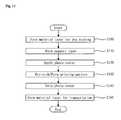
- FIG. 11is a flowchart illustrating a manufacturing method of a printing substrate for a liquid crystal display according to a first embodiment of the present invention.
- FIGS. 12 to 14are views illustrating the respective steps, i.e. step S 100 , step S 110 , and step S 120 of the method as shown in FIG. 11
- FIG. 15is a view illustrating a part of FIG. 14 in more detail.
- the material layer 210 for dry etchingis deposited on the entire surface of the transparent insulating substrate 200 in the step S 100 , as shown in FIG. 12 .
- the support layermay be added on the lower surface of the transparent insulating substrate 200 .
- the material layer 210 for dry etching and support layer 220may be formed of a same material having the same thickness.
- the material layer 210 for dry etching and support layer 220may be formed of a material such as a-Si, SiNx, SiOx, and the like.
- a photo resistPR is applied along the printing pattern on the upper side of the material layer 210 for dry etching in the step S 120 , as shown in FIG. 13 .
- the material layer 210 for dry etchingis dry-etched along the printing pattern using the photo resist (PR) as an etching mask in the step S 130 , as shown in FIG. 14 .
- the printing pattern formed by the material layer 210 for dry etchingmore than about 4 ⁇ m and less than about 10 ⁇ m in width, and more than about 20 ⁇ m and less than about 30 ⁇ m in depth through the dry etching.
- step S 140Stripping the photo resist in step S 140 completes the printing substrate for the liquid crystal display formed with the transparent insulating substrate 200 and the material layer 210 for dry etching which constitutes a pattern on the upper surface of the transparent insulating substrate 200 , as shown in FIG. 8 .
- step S 150where the material layer 230 for transcription may be further added on the entire surface of the transparent insulating substrate 200 comprising the material layer 210 for dry etching.
- the material layer 230 for transcriptionmay be formed of a metal or metal oxide.
- a primary gas used for dry etchingis, for example, C 12 in the case of etching a-Si, and a fluorine-based compound such as SF6, CF4, etc. in the case of etching SiNx or SiOx.
- FIG. 16is a view illustrating a manufacturing method of a printing substrate for a liquid crystal display according to a second embodiment of the present invention.
- the material layer 210 for dry etching or the support layer 220may be manufactured in a film type and attached on the transparent insulating substrate 200 , as shown in FIG. 16 .
- the material layer 210 and support layer 220may be attached using a simple heat treatment process at a temperature less than about 200° C., and may also be formed to be attached without a separate heat treatment process by including an adhesive component.
Landscapes
- Physics & Mathematics (AREA)
- Nonlinear Science (AREA)
- Engineering & Computer Science (AREA)
- Microelectronics & Electronic Packaging (AREA)
- Mathematical Physics (AREA)
- Chemical & Material Sciences (AREA)
- Crystallography & Structural Chemistry (AREA)
- General Physics & Mathematics (AREA)
- Optics & Photonics (AREA)
- Liquid Crystal (AREA)
Abstract
Description
- This application claims the benefit of Korean Patent Application No. 10-2005-0058871, filed on Jun. 30, 2005, which is hereby incorporated by reference for all purposes as if fully set forth herein.
- 1. Field of the Invention
- The present invention relates to a printing substrate for a liquid crystal display and a manufacturing method thereof.
- 2. Discussion of the Related Art
FIG. 1 is a view for illustrating a related art resist printing method.- In the resist printing method of
FIG. 1 , a photo resist pattern P2 is not directly transcribed from a first transparentinsulating substrate 110, on which a printing pattern is patterned to be used as a printing substrate, onto a second transparentinsulating substrate 120, an object to be printed, but instead, the photo resist pattern P2 is first transferred to ablanket 100 whose surface is made of silicon rubber and the like and which serves as a medium, and then is transcribed using the secondinsulating substrate 120 as an object to be transcribed. FIGS. 2 through 7 illustrate the respective steps of a method of manufacturing the printing substrate as shown inFIG. 1 .FIG. 2 shows the step of depositing ametal layer 111 on the transparentinsulating substrate 110,FIG. 3 shows the step of applying a photo resist112 to pattern themetal layer 111,FIG. 4 shows the step of etching themetal layer 111 using a wet eching,FIG. 5 shows the step of striping the photo resist112,FIG. 6 shows the step of forming the printing pattern P1 by etching the firsttransparent insulating substrate 110, andFIG. 7 shows the step of etching and striping themetal layer 111.- In
FIG. 2 , because themetal layer 111 is used as a mask when the first transparentinsulating substrate 110 is etched in the step illustrated inFIG. 6 , the metal layer is made of a material with a tolerance to etchants used to etch the first transparentinsulating substrate 110, such as Cr, Mo, etc. - As such, since the wet etching has an isotropic etching property which shows a uniform etching property without respect to the direction of crystal faces, loss to critical dimension (CD) greatly occurs due to a collective wet etching upon forming the printing pattern P1, and thus this makes it difficult to manufacture a precise printing substrate having minute patterns formed thereon.
- On the contrary, a dry etching performs an etching through the acceleration force and chemical action of ions in a plasma state using a mixed chemical gas, Ar or the like. Therefore, the dry etching has an anisotropic etching property, whereas the wet etching has the isotropic etching property since it is performed in the chemical solution.
- Referring to
FIGS. 4 and 6 , it is an ideal case that the printing pattern P1 on the first transparentinsulating substrate 110 is formed to have an exact width of d1. However, if the printing substrate is manufactured through the wet etching, loss in thickness occurs on both sides of the printing substrate by the factor of d2. As an example, a printing substrate manufactured through the wet etching is theoretically impossible to implement the minimum critical dimension having less than 10 μm with respect to its both sides due to its isotropic etching property in a case where the depth of etching is 5 μm. - That is, as the printing pattern P1 has its narrower width and deeper depth, and greater ratio of depth to width, its printing property becomes better. However, the related art method using the wet etching causes the width to be broadened as the depth increases, and thus is disadvantageous to manufacture a printing substrate with minute patterns, thereby making it difficult to improve pattern resolution and transcription property.
- Accordingly, the present invention is directed to a printing substrate for a liquid crystal display and a manufacturing method thereof that substantially obviates one or more of the problems due to limitations and disadvantages of the related art.
- An advantage of the present invention is to provide a printing substrate for a liquid crystal display which may mitigate the shortcoming of a resist printing process to implement minute patterns and thus improve pattern resolution and transcription property.
- Another advantage of the present invention is to provide a manufacturing method of a printing substrate for a liquid crystal display which may efficiently manufacture a printing substrate for the liquid crystal display.
- Additional features and advantages of the invention will be set forth in the description which follows, and in part will be apparent from the description or may be learned by practice of the invention. These and other advantages of the invention will be likely realized and attained by the structure particularly pointed out in the written description and claims hereof as well as the appended drawings.
- To achieve these and other advantages and in accordance with the purpose of the present invention, as embodied and broadly described, a printing substrate for a liquid crystal display according to an embodiment of the present invention comprises a transparent insulating substrate and a material layer for dry etching formed on an upper surface of the transparent insulating substrate, the material layer for dry etching constituting a printing pattern.
- In addition, to accomplish the above aspects, a manufacturing method of a printing substrate for a liquid crystal display according to another embodiment of the present invention comprises: forming a material layer on an upper surface of a transparent insulating substrate, applying a photo resist along a printing pattern on the upper side of the material layer, dry-etching the material layer along the printing pattern using the photo resist as an etching mask, and stripping the photo resist.
FIG. 1 is a view for illustrating a related art resist printing method.- FIGS.2 to7 are views illustrating the respective steps of a manufacturing method of the printing substrate as shown in
FIG. 1 . FIG. 8 is a view illustrating the printing substrate for the liquid crystal display according to a first embodiment of the present invention.FIG. 9 is a view illustrating the printing substrate for the liquid crystal display according to a second embodiment of the present invention.FIG. 10 is a view illustrating the printing substrate for the liquid crystal display according to a third embodiment of the present invention.FIG. 11 is a flowchart illustrating a manufacturing method of a printing substrate for a liquid crystal display according to a first embodiment of the present invention.- FIGS.12 to14 are views illustrating partial steps in the method as shown in
FIG. 11 . FIG. 15 is a view illustrating a part ofFIG. 14 in more detail.FIG. 16 is a view illustrating a manufacturing method of a printing substrate for a liquid crystal display according to a second embodiment of the present invention.- Reference will now be made in detail to embodiments of the present invention, examples of which are illustrated in the accompanying drawings.
- Hereinafter, a printing substrate for a liquid crystal display according to embodiments of the present invention will be described in more detail with reference to
FIGS. 8 through 10 . FIG. 8 is a view illustrating the printing substrate for the liquid crystal display according to the first embodiment of the present invention.- In
FIG. 8 , the printing substrate for the liquid crystal display according to the first embodiment of the present invention comprises a transparent insulatingsubstrate 200, and amaterial layer 210 for dry etching. Thematerial layer 210 for dry etching constitutes a printing pattern on an upper surface of the transparent insulatingsubstrate 200. - The
material layer 210 for dry etching may be formed of a Si-based material, such as a-Si, SiNx, SiOx, etc., which creates little loss of critical dimension during dry etching and thus performs dry etching well and provides a good transcription property. - In terms of a-Si, the a-Si may be easily deposited through a process such as PECVD (Plasma Enhanced Chemical Vapor Deposition), with a thickness formed of about 3 μm˜30 μm.
- As such, since the printing pattern formed with the
material layer 210 for dry etching leads to little loss of the critical dimension, it is possible to efficiently form minute patterns whose width b1 or b2 is more than about 4 μm and less than about 10 μm, and whose depth a is more than about 20 μm and less than about 30 μm. - In the related art, a metal layer made of Cr and the like has been used as a mask material to etch the transparent insulating
substrate 200. However, an embodiment of the present invention may employ a photo resist (PR) as the mask upon etching the silicon based material such as a-Si, and this makes it more advantageous to apply to the manufacturing process. FIG. 9 is a view illustrating the printing substrate for the liquid crystal display according to a second embodiment of the present invention.- Referring to
FIG. 9 , a printing substrate for a liquid crystal display according to the second embodiment of the present invention comprises a transparent insulatingsubstrate 200, amaterial layer 210 for dry etching, and asupport layer 220. Thematerial layer 210 for dry etching is formed on an upper surface of the transparent insulatingsubstrate 200, and thesupport layer 220 covers a lower surface of the transparent insulatingsubstrate 200. - The printing substrate manufactured as the first embodiment of the present invention has a great thickness in the
material layer 210 for dry etching deposited on the transparent insulatingsubstrate 200, and this may cause bending of the transparent insulatingsubstrate 200 due to the increase of film stress. - To prevent this, the
support layer 220, which may mitigate the increased stress, is deposited on the lower surface of the transparent insulatingsubstrate 200 as shown inFIG. 9 . As an example, if the same material is deposited on both surfaces of the transparent insulatingsubstrate 200, theoretically film stress does not occur, and bending of the transparent insulatingsubstrate 200 is not created. - The same material as the
material layer 210 for dry etching, such as a-Si, SiNx, SiOx, etc. may be deposited as thesupport layer 220 with a same thickness as thematerial layer 210 for dry etching, or another material such as Cr, Mo, Al, etc. may be deposited. FIG. 10 is a view illustrating the printing substrate for the liquid crystal display according to a third embodiment of the present invention.- In
FIG. 10 , a printing substrate for a liquid crystal display according to the third embodiment of the present invention comprises a transparent insulatingsubstrate 200, amaterial layer 210 for dry etching, and amaterial layer 230 for transcription. Thematerial layer 210 for dry etching is formed on an upper surface of the transparent insulatingsubstrate 200 to constitute a printing pattern, and thematerial layer 230 for transcription covers an upper surface of the transparent insulatingsubstrate 200 including thematerial layer 210 for dry etching. - The
material layer 230 for transcription may be formed of a metal or metal oxide. - The printing substrate should have a selection ratio which makes the transcription property good and the photo resist (PR) attached well so as to provide a good transcription from a blanket onto the printing substrate, and from the printing substrate onto the transparent insulating substrate for the liquid crystal display. Forming the printing substrate with the transparent insulating
substrate 200 generally gives a good selection ratio. However, the embodiment of the present invention is deposited with thematerial layer 210 for dry etching such as a-Si, SiNx, SiOx, etc. to implement the critical dimension, and this may lead to a problem to the transcription property. To mitigate the problem, there is deposited thematerial layer 230 for transcription made of a material having a good transcription property on the entire surface of thetransparent insulating substrate 200 formed with thematerial layer 210 for dry etching, as shown inFIG. 10 . - In the first to third embodiments of the present invention, the
material layer 210 for dry etching or thesupport layer 220 may be manufactured in a film type and attached on thetransparent insulating substrate 200. In a case where thematerial layer 210 andsupport layer 220 are manufactured in an acryl-based film, they may be attached through a simple heat treatment process at a temperature less than about 200° C., and may also be formed to be attached without a separate heat treatment process by including an adhesive component. - Further, making the
material layer 210 for dry etching, which constitutes a printing pattern, formed on the transparent insulatingsubstrate 200, and simultaneously making thesupport layer 220 andmaterial layer 230 for transcription formed on upper and lower surfaces thereof, prevents bending of the transparent insulatingsubstrate 200, as well as improves the transcription property. - Hereinafter, a manufacturing method of a printing substrate for a liquid crystal display according to embodiments of the present invention will be described in more detail with reference to
FIGS. 11 through 17 . FIG. 11 is a flowchart illustrating a manufacturing method of a printing substrate for a liquid crystal display according to a first embodiment of the present invention.- FIGS.12 to14 are views illustrating the respective steps, i.e. step S100, step S110, and step S120 of the method as shown in
FIG. 11 , andFIG. 15 is a view illustrating a part ofFIG. 14 in more detail. - First, the
material layer 210 for dry etching is deposited on the entire surface of the transparent insulatingsubstrate 200 in the step S100, as shown inFIG. 12 . - Then, in step S110, the support layer may be added on the lower surface of the transparent insulating
substrate 200. - The
material layer 210 for dry etching andsupport layer 220 may be formed of a same material having the same thickness. In addition, thematerial layer 210 for dry etching andsupport layer 220 may be formed of a material such as a-Si, SiNx, SiOx, and the like. - Next, a photo resist (PR) is applied along the printing pattern on the upper side of the
material layer 210 for dry etching in the step S120, as shown inFIG. 13 . - Subsequently, the
material layer 210 for dry etching is dry-etched along the printing pattern using the photo resist (PR) as an etching mask in the step S130, as shown inFIG. 14 . - The printing pattern formed by the
material layer 210 for dry etching more than about 4 μm and less than about 10 μm in width, and more than about 20 μm and less than about 30 μm in depth through the dry etching. - Stripping the photo resist in step S140 completes the printing substrate for the liquid crystal display formed with the transparent insulating
substrate 200 and thematerial layer 210 for dry etching which constitutes a pattern on the upper surface of the transparent insulatingsubstrate 200, as shown inFIG. 8 . - After stripping the photo resist (PR), in step S150, where the
material layer 230 for transcription may be further added on the entire surface of the transparent insulatingsubstrate 200 comprising thematerial layer 210 for dry etching. - The
material layer 230 for transcription may be formed of a metal or metal oxide. - When the silicon-based material such as the a-Si is etched, there is little loss of the critical dimension, as shown in
FIG. 15 . That is, as shown in the etched portion C, the ends of the photo resist (PR) are nearly brought into line with the ends of thematerial layer 210 for dry etching. A primary gas used for dry etching is, for example, C12 in the case of etching a-Si, and a fluorine-based compound such as SF6, CF4, etc. in the case of etching SiNx or SiOx. - As such, since there is little loss to the critical dimension, it is possible to implement the minute critical dimension in the level of photolithography.
FIG. 16 is a view illustrating a manufacturing method of a printing substrate for a liquid crystal display according to a second embodiment of the present invention.- The
material layer 210 for dry etching or thesupport layer 220 may be manufactured in a film type and attached on the transparent insulatingsubstrate 200, as shown inFIG. 16 . In a case where thematerial layer 210 andsupport layer 220 are manufactured in an acryl-based film, they may be attached using a simple heat treatment process at a temperature less than about 200° C., and may also be formed to be attached without a separate heat treatment process by including an adhesive component. - It will be apparent to those skilled in the art that various modifications and variation can be made in the present invention without departing from the spirit or scope of the invention. Thus, it is intended that the present invention cover the modifications and variations of this invention provided they come within the scope of the appended claims and their equivalents.
Claims (22)
Applications Claiming Priority (2)
| Application Number | Priority Date | Filing Date | Title |
|---|---|---|---|
| KR1020050058871AKR100716304B1 (en) | 2005-06-30 | 2005-06-30 | Printing plate for liquid crystal display device and manufacturing method thereof |
| KR10-2005-0058871 | 2005-06-30 |
Publications (2)
| Publication Number | Publication Date |
|---|---|
| US20070000865A1true US20070000865A1 (en) | 2007-01-04 |
| US8486608B2 US8486608B2 (en) | 2013-07-16 |
Family
ID=37588218
Family Applications (1)
| Application Number | Title | Priority Date | Filing Date |
|---|---|---|---|
| US11/476,806Active2029-06-21US8486608B2 (en) | 2005-06-30 | 2006-06-29 | Printing substrate for liquid crystal display, and manufacturing method thereof |
Country Status (2)
| Country | Link |
|---|---|
| US (1) | US8486608B2 (en) |
| KR (1) | KR100716304B1 (en) |
Cited By (7)
| Publication number | Priority date | Publication date | Assignee | Title |
|---|---|---|---|---|
| US20090056991A1 (en)* | 2007-08-31 | 2009-03-05 | Kuhr Werner G | Methods of Treating a Surface to Promote Binding of Molecule(s) of Interest, Coatings and Devices Formed Therefrom |
| US20090225585A1 (en)* | 2007-12-27 | 2009-09-10 | Hawkins J Adrian | Self-Contained Charge Storage Molecules for Use in Molecular Capacitors |
| US20100009255A1 (en)* | 2008-07-14 | 2010-01-14 | Hawkins J Adrian | Phosphonium Ionic Liquids, Compositions, Methods of Making and Batteries Formed There From |
| US20100071938A1 (en)* | 2007-08-31 | 2010-03-25 | Kuhr Werner G | Methods of treating a surface to promote metal plating and devices formed |
| US8907133B2 (en) | 2008-07-14 | 2014-12-09 | Esionic Es, Inc. | Electrolyte compositions and electrochemical double layer capacitors formed there from |
| US8927775B2 (en) | 2008-07-14 | 2015-01-06 | Esionic Es, Inc. | Phosphonium ionic liquids, salts, compositions, methods of making and devices formed there from |
| US9345149B2 (en) | 2010-07-06 | 2016-05-17 | Esionic Corp. | Methods of treating copper surfaces for enhancing adhesion to organic substrates for use in printed circuit boards |
Families Citing this family (1)
| Publication number | Priority date | Publication date | Assignee | Title |
|---|---|---|---|---|
| WO2011053093A2 (en)* | 2009-11-02 | 2011-05-05 | 엘지이노텍 주식회사 | Printing plate for liquid crystal display and manufacturing method thereof, method for printing using same, and method for manufacturing replication master mold and printing plate using same |
Citations (7)
| Publication number | Priority date | Publication date | Assignee | Title |
|---|---|---|---|---|
| US4241165A (en)* | 1978-09-05 | 1980-12-23 | Motorola, Inc. | Plasma development process for photoresist |
| US5037504A (en)* | 1989-07-25 | 1991-08-06 | Dai Nippon Insatsu Kabushiki Kaisha | Method of forming fine patterns |
| US20010014492A1 (en)* | 2000-02-07 | 2001-08-16 | Lintec Corporation | Process for producing semiconductor chip |
| US20020119665A1 (en)* | 2001-02-23 | 2002-08-29 | Koninklijke Philips Electronics N.V. | Printing plates |
| US20050031861A1 (en)* | 2003-08-08 | 2005-02-10 | Takeshi Matsumura | Re-peelable pressure-sensitive adhesive sheet |
| US20060134406A1 (en)* | 2003-01-22 | 2006-06-22 | Lintec Corporation | Pressure sensitive adhesive sheet, method of protecting semiconductor wafer surface and method of processing work |
| US7105280B1 (en)* | 2002-06-28 | 2006-09-12 | Seagate Technology Llc | Utilizing permanent master for making stampers/imprinters for patterning of recording media |
Family Cites Families (7)
| Publication number | Priority date | Publication date | Assignee | Title |
|---|---|---|---|---|
| JPS5933849A (en)* | 1982-08-20 | 1984-02-23 | Toshiba Corp | Semiconductor device and manufacture thereof |
| JPH0784108B2 (en)* | 1988-09-22 | 1995-09-13 | 凸版印刷株式会社 | Resin or rubber printing plate |
| JPH0743734A (en)* | 1993-07-27 | 1995-02-14 | Dainippon Printing Co Ltd | Method for forming ITO patterning layer |
| KR0154831B1 (en)* | 1995-08-23 | 1998-11-16 | 김광호 | Manufacturing method of liquid crystal cell |
| JPH1092745A (en) | 1996-09-13 | 1998-04-10 | Toshiba Corp | Crystal semiconductor manufacturing method and manufacturing apparatus |
| KR20030057067A (en)* | 2001-12-28 | 2003-07-04 | 엘지.필립스 엘시디 주식회사 | A method of forming pattern using printing process |
| KR100976343B1 (en)* | 2003-12-24 | 2010-08-16 | 엘지디스플레이 주식회사 | Printing plate manufacturing method and liquid crystal display device manufacturing method |
- 2005
- 2005-06-30KRKR1020050058871Apatent/KR100716304B1/ennot_activeExpired - Fee Related
- 2006
- 2006-06-29USUS11/476,806patent/US8486608B2/enactiveActive
Patent Citations (7)
| Publication number | Priority date | Publication date | Assignee | Title |
|---|---|---|---|---|
| US4241165A (en)* | 1978-09-05 | 1980-12-23 | Motorola, Inc. | Plasma development process for photoresist |
| US5037504A (en)* | 1989-07-25 | 1991-08-06 | Dai Nippon Insatsu Kabushiki Kaisha | Method of forming fine patterns |
| US20010014492A1 (en)* | 2000-02-07 | 2001-08-16 | Lintec Corporation | Process for producing semiconductor chip |
| US20020119665A1 (en)* | 2001-02-23 | 2002-08-29 | Koninklijke Philips Electronics N.V. | Printing plates |
| US7105280B1 (en)* | 2002-06-28 | 2006-09-12 | Seagate Technology Llc | Utilizing permanent master for making stampers/imprinters for patterning of recording media |
| US20060134406A1 (en)* | 2003-01-22 | 2006-06-22 | Lintec Corporation | Pressure sensitive adhesive sheet, method of protecting semiconductor wafer surface and method of processing work |
| US20050031861A1 (en)* | 2003-08-08 | 2005-02-10 | Takeshi Matsumura | Re-peelable pressure-sensitive adhesive sheet |
Cited By (19)
| Publication number | Priority date | Publication date | Assignee | Title |
|---|---|---|---|---|
| US20100071938A1 (en)* | 2007-08-31 | 2010-03-25 | Kuhr Werner G | Methods of treating a surface to promote metal plating and devices formed |
| US8323769B2 (en) | 2007-08-31 | 2012-12-04 | Atotech Deutschland Gmbh | Methods of treating a surface to promote metal plating and devices formed |
| US20090056991A1 (en)* | 2007-08-31 | 2009-03-05 | Kuhr Werner G | Methods of Treating a Surface to Promote Binding of Molecule(s) of Interest, Coatings and Devices Formed Therefrom |
| US20100075427A1 (en)* | 2007-08-31 | 2010-03-25 | Kuhr Werner G | Methods of treating a surface to promote metal plating and devices formed |
| US20090225585A1 (en)* | 2007-12-27 | 2009-09-10 | Hawkins J Adrian | Self-Contained Charge Storage Molecules for Use in Molecular Capacitors |
| US20100118598A1 (en)* | 2008-07-14 | 2010-05-13 | Hawkins J Adrian | Phosphonium Ionic Liquids, Compositions, Methods of Making and Electronic Devices Formed There From |
| US8586798B2 (en) | 2008-07-14 | 2013-11-19 | Esionic Es, Inc. | Heat transfer medium, phosphonium ionic liquids, and methods of making |
| US20100006797A1 (en)* | 2008-07-14 | 2010-01-14 | Hawkins J Adrian | Heat Transfer Medium, Phosphonium Ionic Liquids, and Methods of Making |
| US20100006794A1 (en)* | 2008-07-14 | 2010-01-14 | Hawkins J Adrian | Phosphonium Ionic Liquids, Compositions, Methods of Making and Devices Formed There From |
| US20100009255A1 (en)* | 2008-07-14 | 2010-01-14 | Hawkins J Adrian | Phosphonium Ionic Liquids, Compositions, Methods of Making and Batteries Formed There From |
| US8525155B2 (en) | 2008-07-14 | 2013-09-03 | Esionic Es, Inc. | Phosphonium ionic liquids, compositions, methods of making and electronic devices formed there from |
| US8586797B2 (en) | 2008-07-14 | 2013-11-19 | Esionic Es, Inc. | Phosphonium ionic liquids, compositions, methods of making and devices formed there from |
| US20100068604A1 (en)* | 2008-07-14 | 2010-03-18 | Hawkins J Adrian | Phosphonium Ionic Liquids, Compositions, Methods of Making and Electrolytic Films Formed There From |
| US8778534B2 (en) | 2008-07-14 | 2014-07-15 | Esionic Es, Inc. | Phosphonium ionic liquids, compositions, methods of making and batteries formed there from |
| US8846246B2 (en) | 2008-07-14 | 2014-09-30 | Esionic Es, Inc. | Phosphonium ionic liquids, compositions, methods of making and electrolytic films formed there from |
| US8907133B2 (en) | 2008-07-14 | 2014-12-09 | Esionic Es, Inc. | Electrolyte compositions and electrochemical double layer capacitors formed there from |
| US8927775B2 (en) | 2008-07-14 | 2015-01-06 | Esionic Es, Inc. | Phosphonium ionic liquids, salts, compositions, methods of making and devices formed there from |
| US9345149B2 (en) | 2010-07-06 | 2016-05-17 | Esionic Corp. | Methods of treating copper surfaces for enhancing adhesion to organic substrates for use in printed circuit boards |
| US9795040B2 (en) | 2010-07-06 | 2017-10-17 | Namics Corporation | Methods of treating copper surfaces for enhancing adhesion to organic substrates for use in printed circuit boards |
Also Published As
| Publication number | Publication date |
|---|---|
| KR100716304B1 (en) | 2007-05-08 |
| US8486608B2 (en) | 2013-07-16 |
| KR20070003128A (en) | 2007-01-05 |
Similar Documents
| Publication | Publication Date | Title |
|---|---|---|
| US8486608B2 (en) | Printing substrate for liquid crystal display, and manufacturing method thereof | |
| US6458494B2 (en) | Etching method | |
| JP4542524B2 (en) | Printing plate, method for manufacturing printing plate, and method for manufacturing flat panel display device using printing plate | |
| KR101199937B1 (en) | Method of forming photoresist burr edge and method of manufacturing array substrate | |
| US8372749B2 (en) | Printing plate and method for fabricating the same | |
| US8728331B2 (en) | Methods of fabricating imprint mold and of forming pattern using the imprint mold | |
| US8057691B2 (en) | Method of manufacturing printing plate and method of manufacturing liquid crystal display device using the same | |
| US9040230B2 (en) | Resist ink and method of forming pattern using the same | |
| JP2002258486A (en) | Pattern forming method and method of manufacturing liquid crystal display device using the same | |
| US20090170310A1 (en) | Method of forming a metal line of a semiconductor device | |
| JP2002237594A (en) | Thin film transistor, method of manufacturing thin film transistor, and display device including thin film transistor | |
| CN109031742B (en) | Manufacturing method of display substrate, display substrate and display device | |
| KR20100072969A (en) | Method of fabricating cliche for roll print and method of fabricating liquid crystal display device using thereof | |
| KR20110048605A (en) | Cliché for liquid crystal display device and manufacturing method | |
| JP4362275B2 (en) | Thin film transistor manufacturing method | |
| JP5515564B2 (en) | Method for manufacturing stencil mask for ion implantation | |
| KR100840498B1 (en) | Pattern collapse prevention method of semiconductor device | |
| KR101161797B1 (en) | Method for forming micropattern in semiconductor device | |
| CN1971416A (en) | Printing plate, method of manufacturing of printing plate and liquid crystal display device using the same | |
| JP4534763B2 (en) | Manufacturing method of semiconductor device | |
| KR101148112B1 (en) | A cliche for printing ink and a method of fabricatingthereof | |
| US20080248431A1 (en) | Pattern forming method used in semiconductor device manufacturing and method of manufacturing semiconductor device | |
| KR101279470B1 (en) | A cliche for printing ink and a method of fabricating thereof | |
| KR100781445B1 (en) | Metal wiring formation method of semiconductor device | |
| KR100519314B1 (en) | Etching Method of Semiconductor Wafer |
Legal Events
| Date | Code | Title | Description |
|---|---|---|---|
| AS | Assignment | Owner name:LG.PHILIPS LCD CO., LTD., KOREA, REPUBLIC OF Free format text:ASSIGNMENT OF ASSIGNORS INTEREST;ASSIGNORS:YOO, SOON SUNG;KWON, OH NAM;CHO, HEUNG LYUL;REEL/FRAME:018021/0393 Effective date:20060616 | |
| AS | Assignment | Owner name:LG DISPLAY CO., LTD., KOREA, REPUBLIC OF Free format text:CHANGE OF NAME;ASSIGNOR:LG.PHILIPS LCD CO., LTD.;REEL/FRAME:021763/0117 Effective date:20080304 Owner name:LG DISPLAY CO., LTD.,KOREA, REPUBLIC OF Free format text:CHANGE OF NAME;ASSIGNOR:LG.PHILIPS LCD CO., LTD.;REEL/FRAME:021763/0117 Effective date:20080304 | |
| FEPP | Fee payment procedure | Free format text:PAYOR NUMBER ASSIGNED (ORIGINAL EVENT CODE: ASPN); ENTITY STATUS OF PATENT OWNER: LARGE ENTITY | |
| STCF | Information on status: patent grant | Free format text:PATENTED CASE | |
| FPAY | Fee payment | Year of fee payment:4 | |
| MAFP | Maintenance fee payment | Free format text:PAYMENT OF MAINTENANCE FEE, 8TH YEAR, LARGE ENTITY (ORIGINAL EVENT CODE: M1552); ENTITY STATUS OF PATENT OWNER: LARGE ENTITY Year of fee payment:8 | |
| MAFP | Maintenance fee payment | Free format text:PAYMENT OF MAINTENANCE FEE, 12TH YEAR, LARGE ENTITY (ORIGINAL EVENT CODE: M1553); ENTITY STATUS OF PATENT OWNER: LARGE ENTITY Year of fee payment:12 |