US20060292711A1 - Mechanical integrity evaluation of low-k devices with bump shear - Google Patents
Mechanical integrity evaluation of low-k devices with bump shearDownload PDFInfo
- Publication number
- US20060292711A1 US20060292711A1US11/168,837US16883705AUS2006292711A1US 20060292711 A1US20060292711 A1US 20060292711A1US 16883705 AUS16883705 AUS 16883705AUS 2006292711 A1US2006292711 A1US 2006292711A1
- Authority
- US
- United States
- Prior art keywords
- test
- bump
- die
- shear
- interconnect
- Prior art date
- Legal status (The legal status is an assumption and is not a legal conclusion. Google has not performed a legal analysis and makes no representation as to the accuracy of the status listed.)
- Granted
Links
Images


Classifications
- H—ELECTRICITY
- H01—ELECTRIC ELEMENTS
- H01L—SEMICONDUCTOR DEVICES NOT COVERED BY CLASS H10
- H01L22/00—Testing or measuring during manufacture or treatment; Reliability measurements, i.e. testing of parts without further processing to modify the parts as such; Structural arrangements therefor
- H01L22/10—Measuring as part of the manufacturing process
- H01L22/12—Measuring as part of the manufacturing process for structural parameters, e.g. thickness, line width, refractive index, temperature, warp, bond strength, defects, optical inspection, electrical measurement of structural dimensions, metallurgic measurement of diffusions
- G—PHYSICS
- G01—MEASURING; TESTING
- G01R—MEASURING ELECTRIC VARIABLES; MEASURING MAGNETIC VARIABLES
- G01R31/00—Arrangements for testing electric properties; Arrangements for locating electric faults; Arrangements for electrical testing characterised by what is being tested not provided for elsewhere
- G01R31/50—Testing of electric apparatus, lines, cables or components for short-circuits, continuity, leakage current or incorrect line connections
- G01R31/66—Testing of connections, e.g. of plugs or non-disconnectable joints
- G01R31/70—Testing of connections between components and printed circuit boards
- H—ELECTRICITY
- H01—ELECTRIC ELEMENTS
- H01L—SEMICONDUCTOR DEVICES NOT COVERED BY CLASS H10
- H01L22/00—Testing or measuring during manufacture or treatment; Reliability measurements, i.e. testing of parts without further processing to modify the parts as such; Structural arrangements therefor
- H01L22/20—Sequence of activities consisting of a plurality of measurements, corrections, marking or sorting steps
- H—ELECTRICITY
- H01—ELECTRIC ELEMENTS
- H01L—SEMICONDUCTOR DEVICES NOT COVERED BY CLASS H10
- H01L24/00—Arrangements for connecting or disconnecting semiconductor or solid-state bodies; Methods or apparatus related thereto
- H01L24/01—Means for bonding being attached to, or being formed on, the surface to be connected, e.g. chip-to-package, die-attach, "first-level" interconnects; Manufacturing methods related thereto
- H01L24/02—Bonding areas ; Manufacturing methods related thereto
- H01L24/04—Structure, shape, material or disposition of the bonding areas prior to the connecting process
- H01L24/05—Structure, shape, material or disposition of the bonding areas prior to the connecting process of an individual bonding area
- H—ELECTRICITY
- H01—ELECTRIC ELEMENTS
- H01L—SEMICONDUCTOR DEVICES NOT COVERED BY CLASS H10
- H01L24/00—Arrangements for connecting or disconnecting semiconductor or solid-state bodies; Methods or apparatus related thereto
- H01L24/01—Means for bonding being attached to, or being formed on, the surface to be connected, e.g. chip-to-package, die-attach, "first-level" interconnects; Manufacturing methods related thereto
- H01L24/10—Bump connectors ; Manufacturing methods related thereto
- H01L24/12—Structure, shape, material or disposition of the bump connectors prior to the connecting process
- H01L24/13—Structure, shape, material or disposition of the bump connectors prior to the connecting process of an individual bump connector
- H—ELECTRICITY
- H01—ELECTRIC ELEMENTS
- H01L—SEMICONDUCTOR DEVICES NOT COVERED BY CLASS H10
- H01L2224/00—Indexing scheme for arrangements for connecting or disconnecting semiconductor or solid-state bodies and methods related thereto as covered by H01L24/00
- H01L2224/01—Means for bonding being attached to, or being formed on, the surface to be connected, e.g. chip-to-package, die-attach, "first-level" interconnects; Manufacturing methods related thereto
- H01L2224/02—Bonding areas; Manufacturing methods related thereto
- H01L2224/03—Manufacturing methods
- H01L2224/034—Manufacturing methods by blanket deposition of the material of the bonding area
- H01L2224/0346—Plating
- H—ELECTRICITY
- H01—ELECTRIC ELEMENTS
- H01L—SEMICONDUCTOR DEVICES NOT COVERED BY CLASS H10
- H01L2224/00—Indexing scheme for arrangements for connecting or disconnecting semiconductor or solid-state bodies and methods related thereto as covered by H01L24/00
- H01L2224/01—Means for bonding being attached to, or being formed on, the surface to be connected, e.g. chip-to-package, die-attach, "first-level" interconnects; Manufacturing methods related thereto
- H01L2224/02—Bonding areas; Manufacturing methods related thereto
- H01L2224/03—Manufacturing methods
- H01L2224/0347—Manufacturing methods using a lift-off mask
- H—ELECTRICITY
- H01—ELECTRIC ELEMENTS
- H01L—SEMICONDUCTOR DEVICES NOT COVERED BY CLASS H10
- H01L2224/00—Indexing scheme for arrangements for connecting or disconnecting semiconductor or solid-state bodies and methods related thereto as covered by H01L24/00
- H01L2224/01—Means for bonding being attached to, or being formed on, the surface to be connected, e.g. chip-to-package, die-attach, "first-level" interconnects; Manufacturing methods related thereto
- H01L2224/02—Bonding areas; Manufacturing methods related thereto
- H01L2224/04—Structure, shape, material or disposition of the bonding areas prior to the connecting process
- H01L2224/0401—Bonding areas specifically adapted for bump connectors, e.g. under bump metallisation [UBM]
- H—ELECTRICITY
- H01—ELECTRIC ELEMENTS
- H01L—SEMICONDUCTOR DEVICES NOT COVERED BY CLASS H10
- H01L2224/00—Indexing scheme for arrangements for connecting or disconnecting semiconductor or solid-state bodies and methods related thereto as covered by H01L24/00
- H01L2224/01—Means for bonding being attached to, or being formed on, the surface to be connected, e.g. chip-to-package, die-attach, "first-level" interconnects; Manufacturing methods related thereto
- H01L2224/02—Bonding areas; Manufacturing methods related thereto
- H01L2224/04—Structure, shape, material or disposition of the bonding areas prior to the connecting process
- H01L2224/05—Structure, shape, material or disposition of the bonding areas prior to the connecting process of an individual bonding area
- H01L2224/05001—Internal layers
- H01L2224/0501—Shape
- H01L2224/05016—Shape in side view
- H01L2224/05018—Shape in side view being a conformal layer on a patterned surface
- H—ELECTRICITY
- H01—ELECTRIC ELEMENTS
- H01L—SEMICONDUCTOR DEVICES NOT COVERED BY CLASS H10
- H01L2224/00—Indexing scheme for arrangements for connecting or disconnecting semiconductor or solid-state bodies and methods related thereto as covered by H01L24/00
- H01L2224/01—Means for bonding being attached to, or being formed on, the surface to be connected, e.g. chip-to-package, die-attach, "first-level" interconnects; Manufacturing methods related thereto
- H01L2224/02—Bonding areas; Manufacturing methods related thereto
- H01L2224/04—Structure, shape, material or disposition of the bonding areas prior to the connecting process
- H01L2224/05—Structure, shape, material or disposition of the bonding areas prior to the connecting process of an individual bonding area
- H01L2224/05001—Internal layers
- H01L2224/0502—Disposition
- H01L2224/05022—Disposition the internal layer being at least partially embedded in the surface
- H—ELECTRICITY
- H01—ELECTRIC ELEMENTS
- H01L—SEMICONDUCTOR DEVICES NOT COVERED BY CLASS H10
- H01L2224/00—Indexing scheme for arrangements for connecting or disconnecting semiconductor or solid-state bodies and methods related thereto as covered by H01L24/00
- H01L2224/01—Means for bonding being attached to, or being formed on, the surface to be connected, e.g. chip-to-package, die-attach, "first-level" interconnects; Manufacturing methods related thereto
- H01L2224/02—Bonding areas; Manufacturing methods related thereto
- H01L2224/04—Structure, shape, material or disposition of the bonding areas prior to the connecting process
- H01L2224/05—Structure, shape, material or disposition of the bonding areas prior to the connecting process of an individual bonding area
- H01L2224/05001—Internal layers
- H01L2224/0502—Disposition
- H01L2224/05026—Disposition the internal layer being disposed in a recess of the surface
- H01L2224/05027—Disposition the internal layer being disposed in a recess of the surface the internal layer extending out of an opening
- H—ELECTRICITY
- H01—ELECTRIC ELEMENTS
- H01L—SEMICONDUCTOR DEVICES NOT COVERED BY CLASS H10
- H01L2224/00—Indexing scheme for arrangements for connecting or disconnecting semiconductor or solid-state bodies and methods related thereto as covered by H01L24/00
- H01L2224/01—Means for bonding being attached to, or being formed on, the surface to be connected, e.g. chip-to-package, die-attach, "first-level" interconnects; Manufacturing methods related thereto
- H01L2224/02—Bonding areas; Manufacturing methods related thereto
- H01L2224/04—Structure, shape, material or disposition of the bonding areas prior to the connecting process
- H01L2224/05—Structure, shape, material or disposition of the bonding areas prior to the connecting process of an individual bonding area
- H01L2224/05001—Internal layers
- H01L2224/05075—Plural internal layers
- H01L2224/0508—Plural internal layers being stacked
- H01L2224/05084—Four-layer arrangements
- H—ELECTRICITY
- H01—ELECTRIC ELEMENTS
- H01L—SEMICONDUCTOR DEVICES NOT COVERED BY CLASS H10
- H01L2224/00—Indexing scheme for arrangements for connecting or disconnecting semiconductor or solid-state bodies and methods related thereto as covered by H01L24/00
- H01L2224/01—Means for bonding being attached to, or being formed on, the surface to be connected, e.g. chip-to-package, die-attach, "first-level" interconnects; Manufacturing methods related thereto
- H01L2224/02—Bonding areas; Manufacturing methods related thereto
- H01L2224/04—Structure, shape, material or disposition of the bonding areas prior to the connecting process
- H01L2224/05—Structure, shape, material or disposition of the bonding areas prior to the connecting process of an individual bonding area
- H01L2224/05001—Internal layers
- H01L2224/05099—Material
- H01L2224/051—Material with a principal constituent of the material being a metal or a metalloid, e.g. boron [B], silicon [Si], germanium [Ge], arsenic [As], antimony [Sb], tellurium [Te] and polonium [Po], and alloys thereof
- H01L2224/05138—Material with a principal constituent of the material being a metal or a metalloid, e.g. boron [B], silicon [Si], germanium [Ge], arsenic [As], antimony [Sb], tellurium [Te] and polonium [Po], and alloys thereof the principal constituent melting at a temperature of greater than or equal to 950°C and less than 1550°C
- H01L2224/05147—Copper [Cu] as principal constituent
- H—ELECTRICITY
- H01—ELECTRIC ELEMENTS
- H01L—SEMICONDUCTOR DEVICES NOT COVERED BY CLASS H10
- H01L2224/00—Indexing scheme for arrangements for connecting or disconnecting semiconductor or solid-state bodies and methods related thereto as covered by H01L24/00
- H01L2224/01—Means for bonding being attached to, or being formed on, the surface to be connected, e.g. chip-to-package, die-attach, "first-level" interconnects; Manufacturing methods related thereto
- H01L2224/02—Bonding areas; Manufacturing methods related thereto
- H01L2224/04—Structure, shape, material or disposition of the bonding areas prior to the connecting process
- H01L2224/05—Structure, shape, material or disposition of the bonding areas prior to the connecting process of an individual bonding area
- H01L2224/05001—Internal layers
- H01L2224/05099—Material
- H01L2224/051—Material with a principal constituent of the material being a metal or a metalloid, e.g. boron [B], silicon [Si], germanium [Ge], arsenic [As], antimony [Sb], tellurium [Te] and polonium [Po], and alloys thereof
- H01L2224/05163—Material with a principal constituent of the material being a metal or a metalloid, e.g. boron [B], silicon [Si], germanium [Ge], arsenic [As], antimony [Sb], tellurium [Te] and polonium [Po], and alloys thereof the principal constituent melting at a temperature of greater than 1550°C
- H01L2224/05166—Titanium [Ti] as principal constituent
- H—ELECTRICITY
- H01—ELECTRIC ELEMENTS
- H01L—SEMICONDUCTOR DEVICES NOT COVERED BY CLASS H10
- H01L2224/00—Indexing scheme for arrangements for connecting or disconnecting semiconductor or solid-state bodies and methods related thereto as covered by H01L24/00
- H01L2224/01—Means for bonding being attached to, or being formed on, the surface to be connected, e.g. chip-to-package, die-attach, "first-level" interconnects; Manufacturing methods related thereto
- H01L2224/02—Bonding areas; Manufacturing methods related thereto
- H01L2224/04—Structure, shape, material or disposition of the bonding areas prior to the connecting process
- H01L2224/05—Structure, shape, material or disposition of the bonding areas prior to the connecting process of an individual bonding area
- H01L2224/0554—External layer
- H01L2224/05541—Structure
- H—ELECTRICITY
- H01—ELECTRIC ELEMENTS
- H01L—SEMICONDUCTOR DEVICES NOT COVERED BY CLASS H10
- H01L2224/00—Indexing scheme for arrangements for connecting or disconnecting semiconductor or solid-state bodies and methods related thereto as covered by H01L24/00
- H01L2224/01—Means for bonding being attached to, or being formed on, the surface to be connected, e.g. chip-to-package, die-attach, "first-level" interconnects; Manufacturing methods related thereto
- H01L2224/02—Bonding areas; Manufacturing methods related thereto
- H01L2224/04—Structure, shape, material or disposition of the bonding areas prior to the connecting process
- H01L2224/05—Structure, shape, material or disposition of the bonding areas prior to the connecting process of an individual bonding area
- H01L2224/0554—External layer
- H01L2224/0555—Shape
- H01L2224/05556—Shape in side view
- H01L2224/05559—Shape in side view non conformal layer on a patterned surface
- H—ELECTRICITY
- H01—ELECTRIC ELEMENTS
- H01L—SEMICONDUCTOR DEVICES NOT COVERED BY CLASS H10
- H01L2224/00—Indexing scheme for arrangements for connecting or disconnecting semiconductor or solid-state bodies and methods related thereto as covered by H01L24/00
- H01L2224/01—Means for bonding being attached to, or being formed on, the surface to be connected, e.g. chip-to-package, die-attach, "first-level" interconnects; Manufacturing methods related thereto
- H01L2224/02—Bonding areas; Manufacturing methods related thereto
- H01L2224/04—Structure, shape, material or disposition of the bonding areas prior to the connecting process
- H01L2224/05—Structure, shape, material or disposition of the bonding areas prior to the connecting process of an individual bonding area
- H01L2224/0554—External layer
- H01L2224/0556—Disposition
- H01L2224/05571—Disposition the external layer being disposed in a recess of the surface
- H01L2224/05572—Disposition the external layer being disposed in a recess of the surface the external layer extending out of an opening
- H—ELECTRICITY
- H01—ELECTRIC ELEMENTS
- H01L—SEMICONDUCTOR DEVICES NOT COVERED BY CLASS H10
- H01L2224/00—Indexing scheme for arrangements for connecting or disconnecting semiconductor or solid-state bodies and methods related thereto as covered by H01L24/00
- H01L2224/01—Means for bonding being attached to, or being formed on, the surface to be connected, e.g. chip-to-package, die-attach, "first-level" interconnects; Manufacturing methods related thereto
- H01L2224/02—Bonding areas; Manufacturing methods related thereto
- H01L2224/04—Structure, shape, material or disposition of the bonding areas prior to the connecting process
- H01L2224/05—Structure, shape, material or disposition of the bonding areas prior to the connecting process of an individual bonding area
- H01L2224/0554—External layer
- H01L2224/05575—Plural external layers
- H01L2224/0558—Plural external layers being stacked
- H—ELECTRICITY
- H01—ELECTRIC ELEMENTS
- H01L—SEMICONDUCTOR DEVICES NOT COVERED BY CLASS H10
- H01L2224/00—Indexing scheme for arrangements for connecting or disconnecting semiconductor or solid-state bodies and methods related thereto as covered by H01L24/00
- H01L2224/01—Means for bonding being attached to, or being formed on, the surface to be connected, e.g. chip-to-package, die-attach, "first-level" interconnects; Manufacturing methods related thereto
- H01L2224/02—Bonding areas; Manufacturing methods related thereto
- H01L2224/04—Structure, shape, material or disposition of the bonding areas prior to the connecting process
- H01L2224/05—Structure, shape, material or disposition of the bonding areas prior to the connecting process of an individual bonding area
- H01L2224/0554—External layer
- H01L2224/05599—Material
- H01L2224/056—Material with a principal constituent of the material being a metal or a metalloid, e.g. boron [B], silicon [Si], germanium [Ge], arsenic [As], antimony [Sb], tellurium [Te] and polonium [Po], and alloys thereof
- H01L2224/05617—Material with a principal constituent of the material being a metal or a metalloid, e.g. boron [B], silicon [Si], germanium [Ge], arsenic [As], antimony [Sb], tellurium [Te] and polonium [Po], and alloys thereof the principal constituent melting at a temperature of greater than or equal to 400°C and less than 950°C
- H01L2224/05624—Aluminium [Al] as principal constituent
- H—ELECTRICITY
- H01—ELECTRIC ELEMENTS
- H01L—SEMICONDUCTOR DEVICES NOT COVERED BY CLASS H10
- H01L2224/00—Indexing scheme for arrangements for connecting or disconnecting semiconductor or solid-state bodies and methods related thereto as covered by H01L24/00
- H01L2224/01—Means for bonding being attached to, or being formed on, the surface to be connected, e.g. chip-to-package, die-attach, "first-level" interconnects; Manufacturing methods related thereto
- H01L2224/02—Bonding areas; Manufacturing methods related thereto
- H01L2224/04—Structure, shape, material or disposition of the bonding areas prior to the connecting process
- H01L2224/05—Structure, shape, material or disposition of the bonding areas prior to the connecting process of an individual bonding area
- H01L2224/0554—External layer
- H01L2224/05599—Material
- H01L2224/056—Material with a principal constituent of the material being a metal or a metalloid, e.g. boron [B], silicon [Si], germanium [Ge], arsenic [As], antimony [Sb], tellurium [Te] and polonium [Po], and alloys thereof
- H01L2224/05638—Material with a principal constituent of the material being a metal or a metalloid, e.g. boron [B], silicon [Si], germanium [Ge], arsenic [As], antimony [Sb], tellurium [Te] and polonium [Po], and alloys thereof the principal constituent melting at a temperature of greater than or equal to 950°C and less than 1550°C
- H01L2224/05647—Copper [Cu] as principal constituent
- H—ELECTRICITY
- H01—ELECTRIC ELEMENTS
- H01L—SEMICONDUCTOR DEVICES NOT COVERED BY CLASS H10
- H01L2224/00—Indexing scheme for arrangements for connecting or disconnecting semiconductor or solid-state bodies and methods related thereto as covered by H01L24/00
- H01L2224/01—Means for bonding being attached to, or being formed on, the surface to be connected, e.g. chip-to-package, die-attach, "first-level" interconnects; Manufacturing methods related thereto
- H01L2224/02—Bonding areas; Manufacturing methods related thereto
- H01L2224/04—Structure, shape, material or disposition of the bonding areas prior to the connecting process
- H01L2224/05—Structure, shape, material or disposition of the bonding areas prior to the connecting process of an individual bonding area
- H01L2224/0554—External layer
- H01L2224/05599—Material
- H01L2224/056—Material with a principal constituent of the material being a metal or a metalloid, e.g. boron [B], silicon [Si], germanium [Ge], arsenic [As], antimony [Sb], tellurium [Te] and polonium [Po], and alloys thereof
- H01L2224/05663—Material with a principal constituent of the material being a metal or a metalloid, e.g. boron [B], silicon [Si], germanium [Ge], arsenic [As], antimony [Sb], tellurium [Te] and polonium [Po], and alloys thereof the principal constituent melting at a temperature of greater than 1550°C
- H01L2224/05671—Chromium [Cr] as principal constituent
- H—ELECTRICITY
- H01—ELECTRIC ELEMENTS
- H01L—SEMICONDUCTOR DEVICES NOT COVERED BY CLASS H10
- H01L2224/00—Indexing scheme for arrangements for connecting or disconnecting semiconductor or solid-state bodies and methods related thereto as covered by H01L24/00
- H01L2224/01—Means for bonding being attached to, or being formed on, the surface to be connected, e.g. chip-to-package, die-attach, "first-level" interconnects; Manufacturing methods related thereto
- H01L2224/02—Bonding areas; Manufacturing methods related thereto
- H01L2224/04—Structure, shape, material or disposition of the bonding areas prior to the connecting process
- H01L2224/05—Structure, shape, material or disposition of the bonding areas prior to the connecting process of an individual bonding area
- H01L2224/0554—External layer
- H01L2224/05599—Material
- H01L2224/056—Material with a principal constituent of the material being a metal or a metalloid, e.g. boron [B], silicon [Si], germanium [Ge], arsenic [As], antimony [Sb], tellurium [Te] and polonium [Po], and alloys thereof
- H01L2224/05663—Material with a principal constituent of the material being a metal or a metalloid, e.g. boron [B], silicon [Si], germanium [Ge], arsenic [As], antimony [Sb], tellurium [Te] and polonium [Po], and alloys thereof the principal constituent melting at a temperature of greater than 1550°C
- H01L2224/05681—Tantalum [Ta] as principal constituent
- H—ELECTRICITY
- H01—ELECTRIC ELEMENTS
- H01L—SEMICONDUCTOR DEVICES NOT COVERED BY CLASS H10
- H01L2224/00—Indexing scheme for arrangements for connecting or disconnecting semiconductor or solid-state bodies and methods related thereto as covered by H01L24/00
- H01L2224/01—Means for bonding being attached to, or being formed on, the surface to be connected, e.g. chip-to-package, die-attach, "first-level" interconnects; Manufacturing methods related thereto
- H01L2224/02—Bonding areas; Manufacturing methods related thereto
- H01L2224/04—Structure, shape, material or disposition of the bonding areas prior to the connecting process
- H01L2224/05—Structure, shape, material or disposition of the bonding areas prior to the connecting process of an individual bonding area
- H01L2224/0554—External layer
- H01L2224/05599—Material
- H01L2224/056—Material with a principal constituent of the material being a metal or a metalloid, e.g. boron [B], silicon [Si], germanium [Ge], arsenic [As], antimony [Sb], tellurium [Te] and polonium [Po], and alloys thereof
- H01L2224/05663—Material with a principal constituent of the material being a metal or a metalloid, e.g. boron [B], silicon [Si], germanium [Ge], arsenic [As], antimony [Sb], tellurium [Te] and polonium [Po], and alloys thereof the principal constituent melting at a temperature of greater than 1550°C
- H01L2224/05684—Tungsten [W] as principal constituent
- H—ELECTRICITY
- H01—ELECTRIC ELEMENTS
- H01L—SEMICONDUCTOR DEVICES NOT COVERED BY CLASS H10
- H01L2224/00—Indexing scheme for arrangements for connecting or disconnecting semiconductor or solid-state bodies and methods related thereto as covered by H01L24/00
- H01L2224/01—Means for bonding being attached to, or being formed on, the surface to be connected, e.g. chip-to-package, die-attach, "first-level" interconnects; Manufacturing methods related thereto
- H01L2224/10—Bump connectors; Manufacturing methods related thereto
- H01L2224/12—Structure, shape, material or disposition of the bump connectors prior to the connecting process
- H01L2224/13—Structure, shape, material or disposition of the bump connectors prior to the connecting process of an individual bump connector
- H01L2224/13001—Core members of the bump connector
- H01L2224/13005—Structure
- H01L2224/13006—Bump connector larger than the underlying bonding area, e.g. than the under bump metallisation [UBM]
- H—ELECTRICITY
- H01—ELECTRIC ELEMENTS
- H01L—SEMICONDUCTOR DEVICES NOT COVERED BY CLASS H10
- H01L2224/00—Indexing scheme for arrangements for connecting or disconnecting semiconductor or solid-state bodies and methods related thereto as covered by H01L24/00
- H01L2224/01—Means for bonding being attached to, or being formed on, the surface to be connected, e.g. chip-to-package, die-attach, "first-level" interconnects; Manufacturing methods related thereto
- H01L2224/10—Bump connectors; Manufacturing methods related thereto
- H01L2224/12—Structure, shape, material or disposition of the bump connectors prior to the connecting process
- H01L2224/13—Structure, shape, material or disposition of the bump connectors prior to the connecting process of an individual bump connector
- H01L2224/13001—Core members of the bump connector
- H01L2224/13075—Plural core members
- H01L2224/13076—Plural core members being mutually engaged together, e.g. through inserts
- H—ELECTRICITY
- H01—ELECTRIC ELEMENTS
- H01L—SEMICONDUCTOR DEVICES NOT COVERED BY CLASS H10
- H01L2224/00—Indexing scheme for arrangements for connecting or disconnecting semiconductor or solid-state bodies and methods related thereto as covered by H01L24/00
- H01L2224/01—Means for bonding being attached to, or being formed on, the surface to be connected, e.g. chip-to-package, die-attach, "first-level" interconnects; Manufacturing methods related thereto
- H01L2224/10—Bump connectors; Manufacturing methods related thereto
- H01L2224/12—Structure, shape, material or disposition of the bump connectors prior to the connecting process
- H01L2224/13—Structure, shape, material or disposition of the bump connectors prior to the connecting process of an individual bump connector
- H01L2224/13001—Core members of the bump connector
- H01L2224/13099—Material
- H01L2224/131—Material with a principal constituent of the material being a metal or a metalloid, e.g. boron [B], silicon [Si], germanium [Ge], arsenic [As], antimony [Sb], tellurium [Te] and polonium [Po], and alloys thereof
- H01L2224/13101—Material with a principal constituent of the material being a metal or a metalloid, e.g. boron [B], silicon [Si], germanium [Ge], arsenic [As], antimony [Sb], tellurium [Te] and polonium [Po], and alloys thereof the principal constituent melting at a temperature of less than 400°C
- H01L2224/13111—Tin [Sn] as principal constituent
- H—ELECTRICITY
- H01—ELECTRIC ELEMENTS
- H01L—SEMICONDUCTOR DEVICES NOT COVERED BY CLASS H10
- H01L2224/00—Indexing scheme for arrangements for connecting or disconnecting semiconductor or solid-state bodies and methods related thereto as covered by H01L24/00
- H01L2224/01—Means for bonding being attached to, or being formed on, the surface to be connected, e.g. chip-to-package, die-attach, "first-level" interconnects; Manufacturing methods related thereto
- H01L2224/10—Bump connectors; Manufacturing methods related thereto
- H01L2224/12—Structure, shape, material or disposition of the bump connectors prior to the connecting process
- H01L2224/13—Structure, shape, material or disposition of the bump connectors prior to the connecting process of an individual bump connector
- H01L2224/13001—Core members of the bump connector
- H01L2224/13099—Material
- H01L2224/131—Material with a principal constituent of the material being a metal or a metalloid, e.g. boron [B], silicon [Si], germanium [Ge], arsenic [As], antimony [Sb], tellurium [Te] and polonium [Po], and alloys thereof
- H01L2224/13138—Material with a principal constituent of the material being a metal or a metalloid, e.g. boron [B], silicon [Si], germanium [Ge], arsenic [As], antimony [Sb], tellurium [Te] and polonium [Po], and alloys thereof the principal constituent melting at a temperature of greater than or equal to 950°C and less than 1550°C
- H01L2224/13147—Copper [Cu] as principal constituent
- H—ELECTRICITY
- H01—ELECTRIC ELEMENTS
- H01L—SEMICONDUCTOR DEVICES NOT COVERED BY CLASS H10
- H01L2224/00—Indexing scheme for arrangements for connecting or disconnecting semiconductor or solid-state bodies and methods related thereto as covered by H01L24/00
- H01L2224/01—Means for bonding being attached to, or being formed on, the surface to be connected, e.g. chip-to-package, die-attach, "first-level" interconnects; Manufacturing methods related thereto
- H01L2224/10—Bump connectors; Manufacturing methods related thereto
- H01L2224/12—Structure, shape, material or disposition of the bump connectors prior to the connecting process
- H01L2224/13—Structure, shape, material or disposition of the bump connectors prior to the connecting process of an individual bump connector
- H01L2224/1354—Coating
- H01L2224/13599—Material
- H01L2224/136—Material with a principal constituent of the material being a metal or a metalloid, e.g. boron [B], silicon [Si], germanium [Ge], arsenic [As], antimony [Sb], tellurium [Te] and polonium [Po], and alloys thereof
- H—ELECTRICITY
- H01—ELECTRIC ELEMENTS
- H01L—SEMICONDUCTOR DEVICES NOT COVERED BY CLASS H10
- H01L2224/00—Indexing scheme for arrangements for connecting or disconnecting semiconductor or solid-state bodies and methods related thereto as covered by H01L24/00
- H01L2224/01—Means for bonding being attached to, or being formed on, the surface to be connected, e.g. chip-to-package, die-attach, "first-level" interconnects; Manufacturing methods related thereto
- H01L2224/10—Bump connectors; Manufacturing methods related thereto
- H01L2224/12—Structure, shape, material or disposition of the bump connectors prior to the connecting process
- H01L2224/14—Structure, shape, material or disposition of the bump connectors prior to the connecting process of a plurality of bump connectors
- H01L2224/1401—Structure
- H01L2224/1403—Bump connectors having different sizes, e.g. different diameters, heights or widths
- H—ELECTRICITY
- H01—ELECTRIC ELEMENTS
- H01L—SEMICONDUCTOR DEVICES NOT COVERED BY CLASS H10
- H01L2224/00—Indexing scheme for arrangements for connecting or disconnecting semiconductor or solid-state bodies and methods related thereto as covered by H01L24/00
- H01L2224/01—Means for bonding being attached to, or being formed on, the surface to be connected, e.g. chip-to-package, die-attach, "first-level" interconnects; Manufacturing methods related thereto
- H01L2224/10—Bump connectors; Manufacturing methods related thereto
- H01L2224/12—Structure, shape, material or disposition of the bump connectors prior to the connecting process
- H01L2224/14—Structure, shape, material or disposition of the bump connectors prior to the connecting process of a plurality of bump connectors
- H01L2224/1405—Shape
- H01L2224/14051—Bump connectors having different shapes
- H—ELECTRICITY
- H01—ELECTRIC ELEMENTS
- H01L—SEMICONDUCTOR DEVICES NOT COVERED BY CLASS H10
- H01L2224/00—Indexing scheme for arrangements for connecting or disconnecting semiconductor or solid-state bodies and methods related thereto as covered by H01L24/00
- H01L2224/01—Means for bonding being attached to, or being formed on, the surface to be connected, e.g. chip-to-package, die-attach, "first-level" interconnects; Manufacturing methods related thereto
- H01L2224/10—Bump connectors; Manufacturing methods related thereto
- H01L2224/12—Structure, shape, material or disposition of the bump connectors prior to the connecting process
- H01L2224/14—Structure, shape, material or disposition of the bump connectors prior to the connecting process of a plurality of bump connectors
- H01L2224/145—Material
- H01L2224/14505—Bump connectors having different materials
- H—ELECTRICITY
- H01—ELECTRIC ELEMENTS
- H01L—SEMICONDUCTOR DEVICES NOT COVERED BY CLASS H10
- H01L2224/00—Indexing scheme for arrangements for connecting or disconnecting semiconductor or solid-state bodies and methods related thereto as covered by H01L24/00
- H01L2224/01—Means for bonding being attached to, or being formed on, the surface to be connected, e.g. chip-to-package, die-attach, "first-level" interconnects; Manufacturing methods related thereto
- H01L2224/10—Bump connectors; Manufacturing methods related thereto
- H01L2224/12—Structure, shape, material or disposition of the bump connectors prior to the connecting process
- H01L2224/14—Structure, shape, material or disposition of the bump connectors prior to the connecting process of a plurality of bump connectors
- H01L2224/1451—Function
- H01L2224/14515—Bump connectors having different functions
- H—ELECTRICITY
- H01—ELECTRIC ELEMENTS
- H01L—SEMICONDUCTOR DEVICES NOT COVERED BY CLASS H10
- H01L23/00—Details of semiconductor or other solid state devices
- H01L23/28—Encapsulations, e.g. encapsulating layers, coatings, e.g. for protection
- H01L23/31—Encapsulations, e.g. encapsulating layers, coatings, e.g. for protection characterised by the arrangement or shape
- H01L23/3157—Partial encapsulation or coating
- H01L23/3192—Multilayer coating
- H—ELECTRICITY
- H01—ELECTRIC ELEMENTS
- H01L—SEMICONDUCTOR DEVICES NOT COVERED BY CLASS H10
- H01L2924/00—Indexing scheme for arrangements or methods for connecting or disconnecting semiconductor or solid-state bodies as covered by H01L24/00
- H01L2924/0001—Technical content checked by a classifier
- H01L2924/00013—Fully indexed content
- H—ELECTRICITY
- H01—ELECTRIC ELEMENTS
- H01L—SEMICONDUCTOR DEVICES NOT COVERED BY CLASS H10
- H01L2924/00—Indexing scheme for arrangements or methods for connecting or disconnecting semiconductor or solid-state bodies as covered by H01L24/00
- H01L2924/0001—Technical content checked by a classifier
- H01L2924/0002—Not covered by any one of groups H01L24/00, H01L24/00 and H01L2224/00
- H—ELECTRICITY
- H01—ELECTRIC ELEMENTS
- H01L—SEMICONDUCTOR DEVICES NOT COVERED BY CLASS H10
- H01L2924/00—Indexing scheme for arrangements or methods for connecting or disconnecting semiconductor or solid-state bodies as covered by H01L24/00
- H01L2924/01—Chemical elements
- H01L2924/01013—Aluminum [Al]
- H—ELECTRICITY
- H01—ELECTRIC ELEMENTS
- H01L—SEMICONDUCTOR DEVICES NOT COVERED BY CLASS H10
- H01L2924/00—Indexing scheme for arrangements or methods for connecting or disconnecting semiconductor or solid-state bodies as covered by H01L24/00
- H01L2924/01—Chemical elements
- H01L2924/01014—Silicon [Si]
- H—ELECTRICITY
- H01—ELECTRIC ELEMENTS
- H01L—SEMICONDUCTOR DEVICES NOT COVERED BY CLASS H10
- H01L2924/00—Indexing scheme for arrangements or methods for connecting or disconnecting semiconductor or solid-state bodies as covered by H01L24/00
- H01L2924/01—Chemical elements
- H01L2924/01019—Potassium [K]
- H—ELECTRICITY
- H01—ELECTRIC ELEMENTS
- H01L—SEMICONDUCTOR DEVICES NOT COVERED BY CLASS H10
- H01L2924/00—Indexing scheme for arrangements or methods for connecting or disconnecting semiconductor or solid-state bodies as covered by H01L24/00
- H01L2924/01—Chemical elements
- H01L2924/01022—Titanium [Ti]
- H—ELECTRICITY
- H01—ELECTRIC ELEMENTS
- H01L—SEMICONDUCTOR DEVICES NOT COVERED BY CLASS H10
- H01L2924/00—Indexing scheme for arrangements or methods for connecting or disconnecting semiconductor or solid-state bodies as covered by H01L24/00
- H01L2924/01—Chemical elements
- H01L2924/01024—Chromium [Cr]
- H—ELECTRICITY
- H01—ELECTRIC ELEMENTS
- H01L—SEMICONDUCTOR DEVICES NOT COVERED BY CLASS H10
- H01L2924/00—Indexing scheme for arrangements or methods for connecting or disconnecting semiconductor or solid-state bodies as covered by H01L24/00
- H01L2924/01—Chemical elements
- H01L2924/01029—Copper [Cu]
- H—ELECTRICITY
- H01—ELECTRIC ELEMENTS
- H01L—SEMICONDUCTOR DEVICES NOT COVERED BY CLASS H10
- H01L2924/00—Indexing scheme for arrangements or methods for connecting or disconnecting semiconductor or solid-state bodies as covered by H01L24/00
- H01L2924/01—Chemical elements
- H01L2924/01033—Arsenic [As]
- H—ELECTRICITY
- H01—ELECTRIC ELEMENTS
- H01L—SEMICONDUCTOR DEVICES NOT COVERED BY CLASS H10
- H01L2924/00—Indexing scheme for arrangements or methods for connecting or disconnecting semiconductor or solid-state bodies as covered by H01L24/00
- H01L2924/01—Chemical elements
- H01L2924/0105—Tin [Sn]
- H—ELECTRICITY
- H01—ELECTRIC ELEMENTS
- H01L—SEMICONDUCTOR DEVICES NOT COVERED BY CLASS H10
- H01L2924/00—Indexing scheme for arrangements or methods for connecting or disconnecting semiconductor or solid-state bodies as covered by H01L24/00
- H01L2924/01—Chemical elements
- H01L2924/01073—Tantalum [Ta]
- H—ELECTRICITY
- H01—ELECTRIC ELEMENTS
- H01L—SEMICONDUCTOR DEVICES NOT COVERED BY CLASS H10
- H01L2924/00—Indexing scheme for arrangements or methods for connecting or disconnecting semiconductor or solid-state bodies as covered by H01L24/00
- H01L2924/01—Chemical elements
- H01L2924/01074—Tungsten [W]
- H—ELECTRICITY
- H01—ELECTRIC ELEMENTS
- H01L—SEMICONDUCTOR DEVICES NOT COVERED BY CLASS H10
- H01L2924/00—Indexing scheme for arrangements or methods for connecting or disconnecting semiconductor or solid-state bodies as covered by H01L24/00
- H01L2924/01—Chemical elements
- H01L2924/01078—Platinum [Pt]
- H—ELECTRICITY
- H01—ELECTRIC ELEMENTS
- H01L—SEMICONDUCTOR DEVICES NOT COVERED BY CLASS H10
- H01L2924/00—Indexing scheme for arrangements or methods for connecting or disconnecting semiconductor or solid-state bodies as covered by H01L24/00
- H01L2924/01—Chemical elements
- H01L2924/01082—Lead [Pb]
- H—ELECTRICITY
- H01—ELECTRIC ELEMENTS
- H01L—SEMICONDUCTOR DEVICES NOT COVERED BY CLASS H10
- H01L2924/00—Indexing scheme for arrangements or methods for connecting or disconnecting semiconductor or solid-state bodies as covered by H01L24/00
- H01L2924/013—Alloys
- H01L2924/014—Solder alloys
- H—ELECTRICITY
- H01—ELECTRIC ELEMENTS
- H01L—SEMICONDUCTOR DEVICES NOT COVERED BY CLASS H10
- H01L2924/00—Indexing scheme for arrangements or methods for connecting or disconnecting semiconductor or solid-state bodies as covered by H01L24/00
- H01L2924/049—Nitrides composed of metals from groups of the periodic table
- H01L2924/0504—14th Group
- H01L2924/05042—Si3N4
- H—ELECTRICITY
- H01—ELECTRIC ELEMENTS
- H01L—SEMICONDUCTOR DEVICES NOT COVERED BY CLASS H10
- H01L2924/00—Indexing scheme for arrangements or methods for connecting or disconnecting semiconductor or solid-state bodies as covered by H01L24/00
- H01L2924/10—Details of semiconductor or other solid state devices to be connected
- H01L2924/11—Device type
- H01L2924/14—Integrated circuits
- H—ELECTRICITY
- H01—ELECTRIC ELEMENTS
- H01L—SEMICONDUCTOR DEVICES NOT COVERED BY CLASS H10
- H01L2924/00—Indexing scheme for arrangements or methods for connecting or disconnecting semiconductor or solid-state bodies as covered by H01L24/00
- H01L2924/30—Technical effects
- H01L2924/35—Mechanical effects
- H01L2924/351—Thermal stress
- H01L2924/3512—Cracking
Definitions
- the present inventionis directed in general to the field of semiconductor devices.
- the present inventionrelates to a test structure for testing integrated circuits.
- Conductive ball packagingis one type of semiconductor packaging known in the industry as flip chip interconnection.
- the sizes of bond pad regionshave become smaller, resulting in increased stress to the bond pad structure when physical connection is made to the semiconductor die.
- Additional mechanical integrity problemsare created by the interconnect structures used with the manufacturing smaller geometry semiconductors.
- bond pad structures fabricated with copper interconnect metallization and low dielectric constant (low-k) dielectricsare susceptible to mechanical damage during the bonding process, due to the lower Young's modulus and lower fracture toughness of such materials.
- the underlying stack of metal and dielectric layers in such bond pad structuresmay mechanically fracture more easily or otherwise be subject to mismatch stresses (such as generated during die attach process).
- FIG. 1illustrates in cross-sectional form a portion of an integrated circuit having a first exemplary die test structure with a support structure underlying a conductive bump in accordance with various embodiments of the present invention
- FIG. 2illustrates in cross-sectional form a portion of an integrated circuit having a second exemplary die test structure with a support structure underlying a conductive bump in accordance with various embodiments of the present invention
- FIG. 3illustrates in cross-sectional form a portion of an integrated circuit having a third exemplary die test structure with a support structure underlying a conductive bump in accordance with various embodiments of the present invention
- FIG. 4illustrates in cross-sectional form a portion of an integrated circuit having a fourth exemplary die test structure with a support structure underlying a conductive bump in accordance with various embodiments of the present invention
- FIG. 5illustrates a top plan view of a functional die in which one or more mechanical test features have incorporated in accordance with various embodiments of the present invention.
- FIG. 6illustrates in flow chart form an exemplary method for testing the mechanical integrity of one or more wafer die using the bump shear technique in accordance with various embodiments of the present invention.
- a method and apparatusare described for effectively evaluating the integration quality of integrated circuits formed with low dielectric constant (low-k) materials before die packaging occurs, such as by using an improved bond pad structure as a mechanical test feature to provide location-specific integration quality data on one or more locations on a single die.
- low-klow dielectric constant
- the mechanical test procedures of the present inventionmay be used to evaluate the mechanical integrity of any integrated circuit structure, the procedures are especially useful for testing structures that are fabricated with low-k dielectrics.
- low-k interconnect stacksare formed below a metal interconnect pad that is placed at the surface of an integrated circuit where an electrical connection is made from the pad to one or more underlying interconnect layers.
- multiple interconnect layers separated by interlayer dielectricsare formed in a stack to provide the required interconnections between devices in the semiconductor substrate.
- Examples of an interconnect padinclude, but are not limited to, a wire bond pad, a probe pad, a flip-chip bump pad, a test point or other packaging or test pad structures that may require underlying structural support.
- a low modulus materialis a material having a value typically less than sixty GPa (Giga-Pascals)
- a low-k materialis a material having a relative permittivity or dielectric constant typically less than four. It should be noted that many of the low-k dielectrics in use have low moduli.
- the use herein of a high modulus materialis a material having a value typically equal to or greater than sixty GPa (Giga-Pascals). Dielectrics having any modulus value may be used in connection with the methods and structures described herein.
- the mechanical integrity of back end of the line (BEOL) structuresmay be evaluated using an improved bump shear test.
- a die test structureis provided that includes a rigid or stiff structural component, such as a bond pad structure which includes a solder bump with a tall stud (or the stud alone) as part of the under bump metallization (UBM).
- the die test structureis used, alone or in combination with a dedicated support structure formed with a predetermined layout pattern of metallization and dielectric in the interconnect stack underlying the pad, to form an improved mechanical test structure and methodology.
- the bump shear testcan provide detailed and accurate information about the integration robustness on almost any location on a die.
- the load curve and maximum load recorded on the bump shear systemmay be analyzed to characterize the material properties of the low-k material and/or the quality of the BEOL integration.
- a uniform mechanical test structuremay be formed in each die and in different wafers so that meaningful comparisons may be made of test results across different die and different wafers.
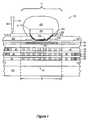
- FIG. 1illustrates in cross-sectional form a portion of an integrated circuit 100 having a first exemplary die test structure 11 that overlies a substrate 102 .
- the substrate 102may be formed of any material, and is typically a semiconductor such as silicon. Within substrate 102 may be formed one or more semiconductor devices (not shown).
- Overlying substrate 102is a plurality of interconnect layer and interlayer dielectrics (ILDs). For example, a last interconnect or last metal (LM) layer 104 overlies a last ILD (LILD) or via layer 16 . The last ILD 16 overlies a next-to-last (LM-1) interconnect or metal line layer 18 .
- ILDsinterconnect layer and interlayer dielectrics
- the next-to-last interconnect layer 18overlies a next-to-last ILD (LILD-1) or via layer 20 .
- the next-to-last ILD 20overlies a second-from-last (LM-2) interconnect layer 22 .
- the second-from-last interconnect layer 22overlies a second-from-last ILD (LILD-2) or via layer 24 .
- the second-from-last ILD 24overlies a third-from-last (LM-3) interconnect layer 26 , and so on.
- the die test structure 11 embodiment depicted in FIG. 1includes a test bump structure 21 which may be formed during fabrication of any conductive bump contacts for the integrated circuit.
- a test bump structure 21which may be formed during fabrication of any conductive bump contacts for the integrated circuit.
- An example of such a fabrication processis described in U.S. Pat. No. 6,413,878 to Woolsey et al. (which is incorporated herein by reference in its entirety), although additional processing steps are required to form the metal cap layer 105 described below.
- the depicted test bump structure 21includes a rigid or stiff structural component 501 (such as a stud formed of copper, tantalum, tungsten, chromium or the like) and a conductive solder ball 502 (such as tin (Sn) and lead (Pb) solder).
- the test bump structuremay be formed of a rigid or stiff structural component (e.g., copper stud only), or alternatively may be formed of only a rigid or stiff conductive solder ball (such as formed with lead-free solder or other high modulus material(s)).
- the test bump structureis integrally attached to the underlying structure, such as by being positioned over and in contact with an optional under bump metallization layer(s) 200 , metal cap 105 or conductive bond pad in the last metal line layer 103 .
- the conductive solder ball 502is solder but may be other electrically conductive materials, including various metal alloys.
- Layer 501may be formed of a high modulus material, such as copper.
- Layer 105may also be optionally provided as a metal cap layer comprised of aluminum (Al) or an alloy thereof, copper (Cu) or an alloy thereof, or a composite of a thin aluminum layer formed on a thinner tantalum layer.
- Layer 103(in the last metal layer) may be optionally provided as a conductive bond pad formed of aluminum (Al), copper (Cu), or the like.
- Alaluminum
- Cucopper
- the conductive solder ball 502is solder but may be other electrically conductive materials, including various metal alloys.
- Layer 501may be formed of a high modulus material, such as copper.
- Layer 105may also be optionally provided as a metal cap layer comprised of aluminum (Al) or an alloy thereof, copper (Cu) or an alloy thereof, or a composite of a thin aluminum layer formed on
- the under bump metallization layer 200various metal layers or composite metal layers may be used, including but not limited to a sputtered and electroplated copper layer formed over a sputtered titanium tungsten (TiW) layer, a NiAu bump layer, a Cr/CrCu bump layer, or the like.
- the under bump metallization layer 200may be optionally provided as a composite metal layer comprising a metal layer 201 (disposed to contact the exposed portion of layer 105 ), a metal layer 202 (disposed or deposited over layer 201 ), and a metal layer 203 (disposed or deposited over layer 202 ).
- Layers 201 and 202may serve as barrier layers, and layer 203 may serve as a seed layer for a subsequent plating step.
- All of layers 201 , 202 , and 203can be sequentially sputtered in-situ to thicknesses of approximately seventy nanometers (nm), approximately two hundred nm, and approximately five hundred nm, respectively.
- layer 201may be formed of a thin layer of titanium tungsten (TiW)
- layer 202may be formed of a thin layer of copper
- layer 203may be formed of a solderable metal comprised of copper.
- a first layer 201 of TiWis sputtered to a first thickness (e.g., 230 nm), then a second layer 202 of Cu is applied to a second thickness (e.g., 530 nm).
- a layer of photoresistis applied at a third thickness (30 um), is patterned to form an opening (e.g., with dimensions of 75 um by 80 um), and a layer of copper is plated to a fourth thickness (e.g., 18 um).
- Insulating layers adjacent to the test bump structure 21are used for passivation of the underlying metal in the last interconnect layer 104 .
- a passivation layer 301may be formed by depositing Si 3 N 4 or SiON over selected portions of the dielectric (e.g., TEOS) in the last interconnect layer 104 and the bonding pad 103 , and then forming an opening or hole in the passivation layer 301 through which electrical and physical contact may be made with the bonding pad 103 (such as by using a metal cap layer 105 ).
- An additional passivation layer 302may optionally be formed of a polyimide layer (to provide a stress buffer) or other passivation materials (such as Si 3 N 4 or SiON) over selected portions of the first passivation layer 301 and metal cap layer 105 , thereby forming an opening or hole through which the under bump metallization layer 200 makes electrical and physical contact with the metal cap layer 105 .
- test bump structures described thus farmay be placed at any interconnect pad site including active circuit contact pads or specially designated test pad locations.
- the test bump structures described hereinprovide an advantage over conventional bump shear tests which apply a shear pin or knife to conventional solder balls which are formed of soft tin/lead solder material.
- Using a stiff bump/stud shear testprovides more accurate information about the underlying integration and can be done on any designated location on the die.
- a stiff bump/studcan apply higher a stress distribution in the BEOL layers on the die than any other test method.
- test bump structures fabricated with copper interconnect metallization and low dielectric constant (low-k) dielectricsare susceptible to differing rates of mechanical fracture that result from the use of low-k interlayer dielectrics that have a lower Young's modulus and lower fracture toughness.
- the metal density within the area defined by 64can be different from the area outside of 64 .
- the metal line density of a typical integrated circuitsuch as that exemplified by the structure outside of the support structure region 64 ) varies randomly, depending on the circuit design layout. Density variations are depicted in FIGS.
- the metal line densitywill also vary laterally from one part of an integrated circuit to another. When such metal density variations exist underneath the test bump structures, it can be difficult to obtain any benchmark reading of the stack strength.
- first and second test pad structuresthat have respective first and second metal densities
- selected embodiments of the present inventionprovide an improved bump shear test by including a dedicated support structure 41 as part of (or below) the test structure 21 , thereby improving the overall toughness and strength of a die test structure 11 formed over a low-k stack.
- the predetermined metal densitymay be determined with reference to the amount of metal in the interconnect layers 18 , 22 , 26 , but may also take into account the amount of metal or other via materials in the via layers 16 , 20 , 24 .
- shear strength testscan also be used to differentiate high yielding die from low yielding die, as well as edge die versus center die, or failing die versus passing die.
- FIG. 1depicts a first example embodiment of the dedicated support structure 41 formed in a support structure region 64 with a predetermined pattern of metal layers 1 , 2 , 3 in one or more of the interconnect layers 18 , 22 , 26 .
- each interconnect layer 18 , 22 , 26includes a parallel-type pattern of metal lines, such as metal lines 1 in the LM-1 layer 18 , metal lines 2 in the LM-2 layer 22 , and metal lines 3 in the LM-3 layer 26 .
- each interconnect layer 18 , 22 , 26includes dielectric layers 45 , 46 , 62 that electrically isolate and separate the metal lines 1 , 2 , 4 .
- the die test structure 11may be strengthened with a forty percent metal-to-dielectric density in the support structure region 41 .
- the predetermined metal densityis fifty-five percent.
- a range for the minimum metal densityis from thirty-five percent to eighty percent, but it should be appreciated that values other than those within this range may adequately provide structural support depending upon the materials used and the layout of the metal lines.
- the dedicated support structure 41may be formed to any desired depth in the integrated circuit 100 .
- a stress boundary 64defines a force region spanning the portion of the integrated circuit directly underlying the conductive bond pad 103 and extending laterally a limited distance.
- the force regionis a region within the integrated circuit 100 in which forces are exerted on the interconnect layers when a bump shear test is performed on the test bump structure 21 .
- the stress boundary 64defines where the stress from the bump shear test is determined to be at or about zero.
- the stress boundary 64defines a cubic force region having lateral dimensions of 140 ⁇ 140 microns centered about the conductive pad 103 .
- the lateral extent of the stress boundaryis advantageously used to locate the die test structure of the present invention on a wafer die so that any mechanical fracture resulting from a bump shear test does not impair the remaining circuit functionality.
- the predetermined pattern of metal layers 1 , 2 , 3 in the support structure 41may require, in some embodiments, that the support structure 41 be mechanically, functionally and/or electrically independent of the remaining circuit.
- the metal layers 1 , 2 , 3 in the interconnect layers 18 , 22 , 26are electrically independent of the remaining circuitry or are electrically grounded. While this feature means that space on an integrated circuit is used for nonfunctioning interconnect layers, the resulting bump shear test benefits obtained from the improved die test structure 11 outweigh any drawback from having unused integrated circuit space.
- the die test structure 11may be used in a bump shear test.
- the shear knife 601When the shear knife 601 is applied or moved laterally against the die test structure 11 so as to intersect with the stiff structural component of the die test structure (e.g., the stud 501 ), increased stress is translated into the die. This increases the likelihood of inducing fracture in the weak interface/film in the die, as compared to conventional bump shear tests, thereby providing a better test for the mechanical integrity of the underlying interconnect layers.
- a shear knife 601 applied at a height of 5 ⁇ mwill apply its force directly through the Cu stud 501 and into the interconnect layers.
- a shear knife that is applied at a height of 20 ⁇ mwill bypass the Cu stud 501 and its force will primarily be applied to the softer solder ball 502 .
- a bump shear testthat aims the shear knife at the stiff structural component will translate the stress from the shear knife into the die to cause inter- or intra-film fracture, thereby providing much meaningful information about the integration of the die interconnect stack.
- a stiff structural componente.g., a copper stud or other material having a modulus meeting or exceeding substantially sixty GPa
- a structural support 41 formed from a predetermined pattern of metal lines in each die test structure 11mechanical die integrity test results from one wafer may be meaningfully compared with mechanical die integrity test results from another wafer.
- This structural support 41accomplishes two things to make this possible. First, the provision of a uniform structural support 41 in the interconnect layers fabricated with copper interconnect metallization and low modulus dielectrics allows a target or baseline level of metal density (e.g., 40%) and strength to be established in each die test structure. Second, when the die test structures in a plurality of wafers or wafer die formed with a shared, predetermined metal line pattern, an apples-to-apples comparison can be made on bump shear tests of the plurality of die test structures.
- the stiff metal studsshould be at least 5 um tall to facilitate bump shear testing.
- a passing bump shear test resultshould only cause the portion of the bump above the UBM to fail during the shear test.
- any fracture below the UBM layerhappens, then it indicates a low-k BEOL failure, which is considered as not a good die.
- the bump shear testremoves all or part of the solder ball (or stud) or the UBM and nothing more, then the test indicates that the die is a “good die.”
- the differences in maximum load and characteristics of the load curvesmay be used to evaluate and compare the multiple die in terms of mechanical integrity, yield and other qualitative measures.
- the disclosed bump shear test structure and methodologymay be used to monitor the under pad low-k BEOL fracture toughness, the quality of adhesion in low-k interconnect layers, variations in dielectric material strength, integration and layout weaknesses, or processing defects that are not detectable during processing (such as uniformity of layer porosity).
- the disclosed test structure and methodis ideal for packaging development and monitoring product quality, especially for devices with low-k dielectric materials that are sensitive to the variance in dielectric material properties AND the quality of the integration. This makes it possible to provide rapid feedback to the die manufacturing facility without running time-consuming package tests and qualifications.
- the disclosed test structure and methodcan be used to evaluate non-low-k devices.
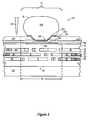
- FIG. 2illustrates in cross-sectional form a portion of an integrated circuit having a second exemplary die test structure 12 with an orthogonal or perpendicular-type support structure 42 underlying a conductive stud 23 in accordance with various embodiments of the present invention.
- the die test structure 12 depicted in FIG. 2includes a test bump structure 23 which may be formed, in some embodiments, during fabrication of any conductive bump contacts for the integrated circuit using the fabrication process substantially as described in U.S. Pat. No. 6,413,878 to Woolsey et al. (except for the formation of the solder bump).
- the depicted test bump structure 23includes only a stiff structural component 503 (such as a copper stud), and does not include a conductive solder ball.
- the stiff structural component 503is preferably formed of a material having a high modulus, and is integrally attached to the underlying structure, such as by being positioned over and in contact with an optional under bump metallization layer(s) 200 , metal cap 105 or conductive bond pad 103 .
- a lower modulus materialmay be used for the test bump structure 23 if the thickness to shear of the structural component 503 is increased.
- the LM-1 layer 18includes one or more metal lines 4 aligned laterally
- the LM-2 layer 22includes one or more metal lines 5 aligned perpendicularly to the metal lines 4
- the LM-3 layer 26includes one or more metal lines 6 aligned perpendicularly to the metal lines 5 and in parallel with the metal lines 4 .
- Such an orthogonal-type pattern of metal lines 42 in the support structure region 64is slightly stiffer than the parallel-type pattern, and provides a better approximation of the mechanical integrity of the remainder of the integrated circuit than is provided by the parallel-type pattern of metal lines.
- FIG. 3shows in cross-sectional form a portion of an integrated circuit having a third exemplary die test structure 13 with a random x-y type pattern support structure 43 underlying a conductive bump 25 in accordance with various embodiments of the present invention.
- the test bump structure 25 depicted in FIG. 3may be formed, in some embodiments, during fabrication of any conductive bump contacts for the integrated circuit using the fabrication process substantially as described in U.S. Pat. No. 6,413,878 to Woolsey et al. (except for the formation of the copper stud).
- the depicted test bump structure 25includes a rigid solder ball component 504 formed from a high modulus material (such as lead-free solder), and does not include a stud.
- a predetermined pattern of metal layers 7 , 8 , 9 formed in the support structure region 64may be a combination of orthogonal and parallel lines configured in a Cartesian or “Manhattan” configuration.
- the LM-1 layer 18includes one or more metal lines 7 aligned orthogonally with respect to each other
- the LM-2 layer 22includes one or more metal lines 8 aligned orthogonally with respect to each other
- the LM-3 layer 26includes one or more metal lines 9 aligned orthogonally with respect to each other.
- a random x-y type pattern of metal lines 43 in the support structure region 64more accurately approximates the mechanical integrity of the remainder of the integrated circuit than the parallel-type or orthogonal-type metal line patterns.
- test bump structuremay be implemented with only a stiff stud 505 , or with only a stiff solder ball 506 , or with a combination of a stiff stud 505 and solder ball 506 (which may or may not be formed of a high modulus material).
- the support structure 44shown in blank box form
- a totally random metal line patternmay be used for the support structure 43 , including but not limited to non-orthogonal-type patterns whereby metal lines are arranged to cross interconnect layers at various angles.
- the support structure 44may include any predetermined layout pattern of metallization and dielectric in the interconnect stack underlying the pad, where the pattern is defined with reference to the metal pattern in the interconnect layers and/or the via pattern in the via layers.
- a selected embodiment of the present inventionprovides a test pad guard structure or ring around the die test structure to protect the die from any fracture damage caused during a bump shear test.
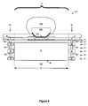
- An example embodimentis illustrated in FIG. 4 , which shows in cross-sectional form one or more guard structures 80 , 90 disposed around a die test structure 14 . By positioning the guard structure(s) 80 , 90 , outside of the force region 78 , the die is protected.
- the guard structures 80 , 90encircle or surround a test bump structure 505 , 506 and a support structure 44 in which any predetermined pattern of metal lines 10 may be formed.
- the guard structureincludes metal lines 81 , 91 formed in the LM layer 71 ; vias 82 , 92 formed in the LILD layer 72 ; metal lines 83 , 93 formed in the LM-1 layer 73 ; vias 84 , 94 formed in the LILD-1 layer 74 ; metal lines 85 , 95 formed in the LM-2 layer 75 ; vias 86 , 96 formed in the LILD-2 layer 76 ; and metal lines 87 , 97 formed in the LM-3 layer 77 .
- additional or fewer metal lines and viasmay be used to form the guard structure.
- the metal lines and viasare formed with copper, except for the bottom via which is formed as a tungsten plug to contact a silicon well region in the substrate (not shown).
- vias between metal layerscan be placed in the underlying support structure 44 to connect the metal lines to the substrate 102 for purposes of avoiding electrical discharging during subsequent processing.
- contact to the substrate 102could be made by connecting one end of the metal lines to the guard structure that connects to the substrate 102 .
- the viasbe placed at an edge of the support structure 44 . If placement of vias within support structure 44 is done, the increase in the complexity of the structure increases the complexity of identifying a failure mode.
- the dedicated die test structure disclosed hereinmay advantageously be incorporated at any desired location on a wafer, including on a functional die or a wafer die scribe, street or any desired location on the wafer, even if there is no functional integrated circuitry at that location.
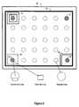
- the die test structures of the present inventionmay be used as dedicated test bump locations on a functional die to provide a mechanical test feature for each die. This is illustrated in FIG. 5 , which shows a top plan view of a functional die 50 in which one or more embodiments of a die test structure have been incorporated in accordance with various embodiments of the present invention.
- one or more special dummy or test bumps 51 , 53 , 55 , 57 with stiff metal studs (or metal stud only)are placed on the die 50 in specific locations (e.g., the corners). While the support structures for each test bump (or stud) may have an identical, predetermined metal line pattern, the support structures can also be different for different dummy bumps (or studs). In addition, the test bumps may be located outside of the functional die circuitry.
- each test bumpmay be determined with reference to the force region for that test bump.
- a stress boundary 58 for a first test bump 53defines the force region for that test bump, and is used to place the test bump 53 away from any other circuitry in the die 50 so that any mechanical fracture caused by a bump shear test of the test bump 53 does not affect the remainder of the die circuitry.
- a guard structure or ringmay be used to physically isolate the test bumps.
- guard ring 54may be formed around a test bump (e.g., test bump 51 )
- the die protection functionmay also be achieved by tying a guard structure 56 to an existing fracture-prevention structure in the die, such as the moisture/metal diffusion barrier 52 formed about the periphery of the die 50 .
- This implementationis illustrated at test bump 55 , where the guard structure 56 , in combination with the edge seal 52 (which acts as a diffusion barrier and crack stop), protects the remainder of the die from any mechanical fracture induced during bump shear testing of the test bump 55 .
- the number of variance tests per die or wafermay be increased.
- between one and four die test structuresare included on each die for use in performing in-line integrity monitoring.
- the bump shear testsmay effectively evaluate the mechanical integrity of the different interconnect regions.
- the four corner die test structures on each diecan thus serve as the equivalent of several hundred conventional die tests that use die pull or other full die test techniques.
- FIG. 6illustrates in flow chart form an example method for testing the mechanical integrity of one or more wafer die using the bump shear technique, die test structure and support structure as variously described herein. Though selected embodiments of the mechanical integrity test methodology are illustrated in FIG. 6 , it will be appreciated by those of ordinary skill in the art that the sequence of illustrated steps may be modified, reduced or augmented in keeping with the disclosure of the present invention. For example, any one or more of the steps may optionally be included or excluded. Thus, it will be appreciated that the methodology of the present invention may be thought of as performing the identified sequence of steps in the order depicted in FIG. 6 , though the steps may also be performed in parallel, in a different order, or as independent operations that are combined.
- the description of the illustrative methodologies for performing bump shear testing with a stiff die test structurecan begin at step 630 , where the die test structure is designed for fabrication on one or more die.
- the design step 630may include specifying one or more design parameters, such as defining a force region 631 , specifying a solder ball/stud structure 632 , defining a metallization pattern for the interconnect layers in the support structure 633 and/or defining a guard structure or ring for the die test structure 634 .
- the die test structureis defined to include a copper stud (with a diameter of 80 ⁇ m and a height of at least 5 ⁇ m) formed over a copper bond pad (75 ⁇ m ⁇ 75 ⁇ m) with an orthogonal-type support structure in one or more of the interconnect layers.
- a bump shear testmay be performed on the die test structure (step 640 ).
- the shear knifeshould be positioned to intersect with the stiff structural component of the die test structure. In other words, the shear knife should be aimed at the stud. In this way, the mechanical integrity of the underlying support layers may be evaluated since this approach applies the lateral force from the shear knife to the support layers instead of primarily impacting only the softer solder ball material.
- the bump shear test on the die test structuremay be performed on the wafer prior to singulation of the wafer into individual die and prior to encapsulation or packaging.
- the bump shear testmay be performed on a test structure located on a “dummy” die that has no functioning integrated circuitry, thereby providing data on the mechanical integrity of the stack on the dummy die which would be representative of functional die.
- the bump shear testmay be performed on a test structure that is located in a scribe area of a wafer, thereby providing test results without sacrificing functioning die.
- the bump shear test resultsare assessed at step 650 . This may be done with a visual inspection of the die test structure to see which layers were fractured by the bump shear test. For example, if only the solder ball and/or copper stud are removed or sheared by the test, then the underlying support structures have the desired mechanical integrity, and the die passes 680 (affirmative outcome to decision 660 ). However, if any part of the underlying support structure (or even the copper bond pad or metal cap layer) is fractured by the bump shear test, then the underlying support structures does not have the desired mechanical integrity, and the die fails 670 (negative outcome to decision 660 ). The bump shear test may the performed on the next die (step 690 ).
- the bump shear test resultsmay also be assessed at step 650 by comparing the bump shear test results with the load curve and maximum load recorded in a database of bump shear measurements to qualitatively characterize the material properties of the underlying support layers, which may be formed from low-k materials. If the test result passes the comparison analysis (affirmative outcome to decision 660 ), then the die passes 680 . Otherwise (negative outcome to decision 660 ), the die fails 670 .
- a bump shear techniquefor evaluating the mechanical integrity of interconnect layers in an integrated circuit for mechanical integrity.
- an integrated circuit having a die test structureis mounted on a test device.
- the die test structureincludes a stiff structural component positioned above and affixed to a conductive metal pad formed in a last metal layer.
- the die test structureis formed as a solder ball formed with a high modulus material (such as lead-free solder), as a solder ball containing a high modulus stud, or as a stud formed with a high modulus material such as copper, tantalum, tungsten or chromium.
- the die test structuremay include a dedicated support structure that is formed with a plurality of low-k dielectric layers in a force region below the conductive metal pad.
- the support structuremay be formed as a predetermined pattern (e.g., parallel, orthogonal or random) of metal lines formed in one or more interconnect layers in the integrated circuit.
- the integrated circuitmay also include a guard structure disposed in the interconnect layers and outside of a force region to protect the integrated circuit from any fractures in the die test structure.
- a guard structuredisposed in the interconnect layers and outside of a force region to protect the integrated circuit from any fractures in the die test structure.
- a testing methodfor measuring the mechanical integrity of an integrated circuit formed with a low-k interconnect stack.
- an integrated circuitis fabricated with a die test structure that includes a stiff structural component affixed over a conductive metal pad formed in an upper layer of the low-k interconnect stack.
- the stiff structural componentmay be formed as a solder bump and an internal stud structure formed of a stiff material, as a stud structure alone or as a solder bump formed of a high modulus material.
- the die test structuremay include a dedicated support structure formed with a predetermined layout pattern of metallization and dielectric in the interconnect stack underlying and affixed to the conductive metal pad.
- a bump shear testis performed on the die test structure by aiming a shear knife at the stiff structural component.
- the mechanical integrity of the integrated circuitis then assessed to determine whether the integrated circuit passes the bump shear test. If only the stiff structural component is removed or sheared by the test, then the underlying support structures in the integrated circuit have the desired mechanical integrity, and the die passes. However, if any part of the underlying support structure is fractured by the bump shear test, then the underlying support structures does not have the desired mechanical integrity, and the die fails.
- an integrated circuit structure and fabrication methodfor forming a die test structure over a substrate.
- a low-k interconnect stackis formed over the substrate, where the low-k interconnect stack includes a dedicated support structure having a predetermined pattern of metal lines in a plurality of interconnect layers.
- a bond padis then formed in a last metal layer of the low-k interconnect stack, and one or more under bump metallization layers formed over and attached to the bond pad.
- a copper studis formed over and attached to the under bump metallization layer, where the height of the copper stud is selected to contact a shear knife during a bump shear test.
- the die test structuremay also include a test pad guard structure formed around at least part of the die test structure to protect the integrated circuit from any fracture damage caused during a bump shear test.
- transistorsmay be formed with various gate electrode formation, extension implant, halo implant, spacer formation, and source/drain implant steps may be performed to complete the transistors.
- conventional backend processingtypically including multiple levels of interconnect is then required to connect the transistors in a desired manner to achieve the desired functionality.
Landscapes
- Engineering & Computer Science (AREA)
- Computer Hardware Design (AREA)
- Microelectronics & Electronic Packaging (AREA)
- Power Engineering (AREA)
- Manufacturing & Machinery (AREA)
- Physics & Mathematics (AREA)
- General Physics & Mathematics (AREA)
- Testing Or Measuring Of Semiconductors Or The Like (AREA)
- Internal Circuitry In Semiconductor Integrated Circuit Devices (AREA)
Abstract
Description
- 1. Field of the Invention
- The present invention is directed in general to the field of semiconductor devices. In one aspect, the present invention relates to a test structure for testing integrated circuits.
- 2. Description of the Related Art
- The use of conductive balls, such as solder balls, to make electrical connection to a bond pad is a known method to make electrical connection to electrical circuitry of a semiconductor die. Conductive ball packaging is one type of semiconductor packaging known in the industry as flip chip interconnection. As geometries in semiconductors continue to shrink in size due to improvements in the technology for making semiconductors, the sizes of bond pad regions have become smaller, resulting in increased stress to the bond pad structure when physical connection is made to the semiconductor die. Additional mechanical integrity problems are created by the interconnect structures used with the manufacturing smaller geometry semiconductors. For example, bond pad structures fabricated with copper interconnect metallization and low dielectric constant (low-k) dielectrics are susceptible to mechanical damage during the bonding process, due to the lower Young's modulus and lower fracture toughness of such materials. As a result, the underlying stack of metal and dielectric layers in such bond pad structures may mechanically fracture more easily or otherwise be subject to mismatch stresses (such as generated during die attach process).
- To detect such device defects, a variety of techniques have been proposed for characterizing the properties and the integration capability of these films, such as nano-indentation and four-point bend delamination tests for mechanical and adhesion properties, and die pull tests and thermal cycling tests for characterizing the behavior of low-k films in a flip chip package. However, these tests have one or more drawbacks in failing to quickly and reliably provide feedback on the quality of the mechanical integration of the back end of the line (BEOL) structures.
- Accordingly, there is a need for improved semiconductor processes and devices to overcome the problems in the art, such as outlined above. Further limitations and disadvantages of conventional processes and technologies will become apparent to one of skill in the art after reviewing the remainder of the present application with reference to the drawings and detailed description which follow.
- The present invention may be understood, and its numerous objects, features and advantages obtained, when the following detailed description of a preferred embodiment is considered in conjunction with the following drawings, in which:
FIG. 1 illustrates in cross-sectional form a portion of an integrated circuit having a first exemplary die test structure with a support structure underlying a conductive bump in accordance with various embodiments of the present invention;FIG. 2 illustrates in cross-sectional form a portion of an integrated circuit having a second exemplary die test structure with a support structure underlying a conductive bump in accordance with various embodiments of the present invention;FIG. 3 illustrates in cross-sectional form a portion of an integrated circuit having a third exemplary die test structure with a support structure underlying a conductive bump in accordance with various embodiments of the present invention;FIG. 4 illustrates in cross-sectional form a portion of an integrated circuit having a fourth exemplary die test structure with a support structure underlying a conductive bump in accordance with various embodiments of the present invention;FIG. 5 illustrates a top plan view of a functional die in which one or more mechanical test features have incorporated in accordance with various embodiments of the present invention; andFIG. 6 illustrates in flow chart form an exemplary method for testing the mechanical integrity of one or more wafer die using the bump shear technique in accordance with various embodiments of the present invention.- It will be appreciated that for simplicity and clarity of illustration, elements illustrated in the drawings have not necessarily been drawn to scale. For example, the dimensions of some of the elements are exaggerated relative to other elements for purposes of promoting and improving clarity and understanding. Further, where considered appropriate, reference numerals have been repeated among the drawings to represent corresponding or analogous elements.
- A method and apparatus are described for effectively evaluating the integration quality of integrated circuits formed with low dielectric constant (low-k) materials before die packaging occurs, such as by using an improved bond pad structure as a mechanical test feature to provide location-specific integration quality data on one or more locations on a single die. Various details are set forth in the following description, but it will be appreciated that the present invention may be practiced without these specific details, and that numerous implementation-specific decisions may be made to the invention described herein to achieve the device designer's specific goals, such as compliance with process technology or design-related constraints, which will vary from one implementation to another. While such a development effort might be complex and time-consuming, it would nevertheless be a routine undertaking for those of ordinary skill in the art having the benefit of this disclosure. For example, selected aspects are depicted with reference to simplified cross sectional drawings of a semiconductor device without including every device feature or geometry in order to avoid obscuring the present invention. Such descriptions and representations are used by those skilled in the art to describe and convey the substance of their work to others skilled in the art. While various illustrative embodiments of the present invention will now be described in detail with reference to
FIGS. 1-6 , it is noted that the various layers of materials will be fabricated by selective deposition and/or removal steps. Where the specific procedures for depositing and removing such layers are not detailed below, conventional techniques known to those skilled in the art for depositing, removing, masking, etching or otherwise forming such layers at appropriate thicknesses may be used. Such details are well known and not considered necessary to teach one skilled in the art of how to make or use the present invention. - While the mechanical test procedures of the present invention may be used to evaluate the mechanical integrity of any integrated circuit structure, the procedures are especially useful for testing structures that are fabricated with low-k dielectrics. For example, low-k interconnect stacks are formed below a metal interconnect pad that is placed at the surface of an integrated circuit where an electrical connection is made from the pad to one or more underlying interconnect layers. In a typical integrated circuit design, multiple interconnect layers separated by interlayer dielectrics are formed in a stack to provide the required interconnections between devices in the semiconductor substrate. Examples of an interconnect pad include, but are not limited to, a wire bond pad, a probe pad, a flip-chip bump pad, a test point or other packaging or test pad structures that may require underlying structural support. Because the advanced low-k interlayer dielectrics used today have a lower dielectric constant and lower Young's modulus than dielectrics used in earlier generation products, integrated circuit structures may more easily mechanically fracture the underlying stack of metal and dielectric layers. As will be appreciated, a low modulus material is a material having a value typically less than sixty GPa (Giga-Pascals), and a low-k material is a material having a relative permittivity or dielectric constant typically less than four. It should be noted that many of the low-k dielectrics in use have low moduli. The use herein of a high modulus material is a material having a value typically equal to or greater than sixty GPa (Giga-Pascals). Dielectrics having any modulus value may be used in connection with the methods and structures described herein.
- In a selected embodiment, the mechanical integrity of back end of the line (BEOL) structures (including but not limited to low-k structures) may be evaluated using an improved bump shear test. Under the test, a die test structure is provided that includes a rigid or stiff structural component, such as a bond pad structure which includes a solder bump with a tall stud (or the stud alone) as part of the under bump metallization (UBM). The die test structure is used, alone or in combination with a dedicated support structure formed with a predetermined layout pattern of metallization and dielectric in the interconnect stack underlying the pad, to form an improved mechanical test structure and methodology. By setting the parameters of the shear process (such as the shear knife speed, height, etc.) so that the shear knife is aimed at the rigid or stiff structural component that is effectively integrated with the underlying support structure, the bump shear test can provide detailed and accurate information about the integration robustness on almost any location on a die. Once the bump shear test procedures are calibrated, the load curve and maximum load recorded on the bump shear system may be analyzed to characterize the material properties of the low-k material and/or the quality of the BEOL integration. In addition, by using predetermined layout patterns in the metallization and dielectric stack underlying the pad, a uniform mechanical test structure may be formed in each die and in different wafers so that meaningful comparisons may be made of test results across different die and different wafers.
FIG. 1 illustrates in cross-sectional form a portion of an integrated circuit100 having a first exemplarydie test structure 11 that overlies asubstrate 102. Thesubstrate 102 may be formed of any material, and is typically a semiconductor such as silicon. Withinsubstrate 102 may be formed one or more semiconductor devices (not shown).Overlying substrate 102 is a plurality of interconnect layer and interlayer dielectrics (ILDs). For example, a last interconnect or last metal (LM)layer 104 overlies a last ILD (LILD) or vialayer 16. The last ILD16 overlies a next-to-last (LM-1) interconnect ormetal line layer 18. The next-to-last interconnect layer 18 overlies a next-to-last ILD (LILD-1) or vialayer 20. The next-to-last ILD 20 overlies a second-from-last (LM-2)interconnect layer 22. The second-from-last interconnect layer 22 overlies a second-from-last ILD (LILD-2) or vialayer 24. The second-from-last ILD24 overlies a third-from-last (LM-3)interconnect layer 26, and so on.- The die
test structure 11 embodiment depicted inFIG. 1 includes atest bump structure 21 which may be formed during fabrication of any conductive bump contacts for the integrated circuit. An example of such a fabrication process is described in U.S. Pat. No. 6,413,878 to Woolsey et al. (which is incorporated herein by reference in its entirety), although additional processing steps are required to form themetal cap layer 105 described below. The depictedtest bump structure 21 includes a rigid or stiff structural component501 (such as a stud formed of copper, tantalum, tungsten, chromium or the like) and a conductive solder ball502 (such as tin (Sn) and lead (Pb) solder). Alternatively and as described below, the test bump structure may be formed of a rigid or stiff structural component (e.g., copper stud only), or alternatively may be formed of only a rigid or stiff conductive solder ball (such as formed with lead-free solder or other high modulus material(s)). The test bump structure is integrally attached to the underlying structure, such as by being positioned over and in contact with an optional under bump metallization layer(s)200,metal cap 105 or conductive bond pad in the lastmetal line layer 103. - In the illustrated embodiment, the
conductive solder ball 502 is solder but may be other electrically conductive materials, including various metal alloys.Layer 501 may be formed of a high modulus material, such as copper.Layer 105 may also be optionally provided as a metal cap layer comprised of aluminum (Al) or an alloy thereof, copper (Cu) or an alloy thereof, or a composite of a thin aluminum layer formed on a thinner tantalum layer. Layer103 (in the last metal layer) may be optionally provided as a conductive bond pad formed of aluminum (Al), copper (Cu), or the like. However, it should be well understood that various metals may be used with the structure described herein. - As for the under
bump metallization layer 200, various metal layers or composite metal layers may be used, including but not limited to a sputtered and electroplated copper layer formed over a sputtered titanium tungsten (TiW) layer, a NiAu bump layer, a Cr/CrCu bump layer, or the like. For example, the underbump metallization layer 200 may be optionally provided as a composite metal layer comprising a metal layer201 (disposed to contact the exposed portion of layer105), a metal layer202 (disposed or deposited over layer201), and a metal layer203 (disposed or deposited over layer202).Layers layer 203 may serve as a seed layer for a subsequent plating step. All oflayers layer 201 may be formed of a thin layer of titanium tungsten (TiW),layer 202 may be formed of a thin layer of copper andlayer 203 may be formed of a solderable metal comprised of copper. For example, afirst layer 201 of TiW is sputtered to a first thickness (e.g., 230 nm), then asecond layer 202 of Cu is applied to a second thickness (e.g., 530 nm). Next, a layer of photoresist is applied at a third thickness (30 um), is patterned to form an opening (e.g., with dimensions of 75 um by 80 um), and a layer of copper is plated to a fourth thickness (e.g., 18 um). - Insulating layers adjacent to the
test bump structure 21 are used for passivation of the underlying metal in thelast interconnect layer 104. For example, apassivation layer 301 may be formed by depositing Si3N4or SiON over selected portions of the dielectric (e.g., TEOS) in thelast interconnect layer 104 and thebonding pad 103, and then forming an opening or hole in thepassivation layer 301 through which electrical and physical contact may be made with the bonding pad103 (such as by using a metal cap layer105). Anadditional passivation layer 302 may optionally be formed of a polyimide layer (to provide a stress buffer) or other passivation materials (such as Si3N4or SiON) over selected portions of thefirst passivation layer 301 andmetal cap layer 105, thereby forming an opening or hole through which the underbump metallization layer 200 makes electrical and physical contact with themetal cap layer 105. - The test bump structures described thus far may be placed at any interconnect pad site including active circuit contact pads or specially designated test pad locations. The test bump structures described herein provide an advantage over conventional bump shear tests which apply a shear pin or knife to conventional solder balls which are formed of soft tin/lead solder material. Using a stiff bump/stud shear test provides more accurate information about the underlying integration and can be done on any designated location on the die. Also, a stiff bump/stud can apply higher a stress distribution in the BEOL layers on the die than any other test method.
- While bump shear testing may be improved by using a stiff bump/stud shear test structure, test bump structures fabricated with copper interconnect metallization and low dielectric constant (low-k) dielectrics are susceptible to differing rates of mechanical fracture that result from the use of low-k interlayer dielectrics that have a lower Young's modulus and lower fracture toughness. The metal density within the area defined by64 can be different from the area outside of64. In particular, it will be appreciated that the metal line density of a typical integrated circuit (such as that exemplified by the structure outside of the support structure region64) varies randomly, depending on the circuit design layout. Density variations are depicted in
FIGS. 1-3 in the part of the integrated circuit that is outside ofsupport structure region 64, where thelast interconnect layer 104 has a first metal line density defined with reference to theconductive bond pad 103, the LM-1interconnect layer 18 has a second metal line density defined with reference to the metal line36, the LM-2interconnect layer 22 has a third metal line density defined with reference to the metal lines47, and the LM-3interconnect layer 26 has a fourth metal line density defined with reference to the metal line60. In addition to the variation in metal line density from one interconnect layer to another, the metal line density will also vary laterally from one part of an integrated circuit to another. When such metal density variations exist underneath the test bump structures, it can be difficult to obtain any benchmark reading of the stack strength. For example, if shear test measurements are conducted on first and second test pad structures that have respective first and second metal densities, it can not be determined if any difference in the test results is caused by the differing metal densities (higher densities tend to be stronger) or by some other defect in the fabrication process. - Accordingly, selected embodiments of the present invention provide an improved bump shear test by including a
dedicated support structure 41 as part of (or below) thetest structure 21, thereby improving the overall toughness and strength of adie test structure 11 formed over a low-k stack. By providing each wafer or wafer die with test bump structure that includes adedicated support structure 41 having a predetermined metal density or amount of metal present in the interconnect layers below thetest bump structure 21, bump shear testing on the different wafers or wafer die can be used to meaningfully compare and evaluate the different wafers or wafer die. As will be appreciated, the predetermined metal density may be determined with reference to the amount of metal in the interconnect layers18,22,26, but may also take into account the amount of metal or other via materials in the via layers16,20,24. In addition to evaluating mechanical integrity, shear strength tests can also be used to differentiate high yielding die from low yielding die, as well as edge die versus center die, or failing die versus passing die. FIG. 1 depicts a first example embodiment of thededicated support structure 41 formed in asupport structure region 64 with a predetermined pattern ofmetal layers interconnect layer metal lines 1 in the LM-1layer 18,metal lines 2 in the LM-2layer 22, andmetal lines 3 in the LM-3layer 26. In the embodiment shown, eachinterconnect layer dielectric layers metal lines metal layers die test structure 11 may be improved. For example, thedie test structure 11 may be strengthened with a forty percent metal-to-dielectric density in thesupport structure region 41. In another embodiment, the predetermined metal density is fifty-five percent. Generally, a range for the minimum metal density is from thirty-five percent to eighty percent, but it should be appreciated that values other than those within this range may adequately provide structural support depending upon the materials used and the layout of the metal lines. Because the parallel-type pattern of metal lines may be included in one or more interconnect layers, thededicated support structure 41 may be formed to any desired depth in the integrated circuit100.- As for the lateral extent of the
support structure 41, astress boundary 64 defines a force region spanning the portion of the integrated circuit directly underlying theconductive bond pad 103 and extending laterally a limited distance. The force region is a region within the integrated circuit100 in which forces are exerted on the interconnect layers when a bump shear test is performed on thetest bump structure 21. Thestress boundary 64 defines where the stress from the bump shear test is determined to be at or about zero. While the shape and contour of the force region may be arbitrarily defined, depending upon device technology and geometries, in an exemplary embodiment involving a squareconductive pad 103 having lateral dimensions of 75×75 microns, thestress boundary 64 defines a cubic force region having lateral dimensions of 140×140 microns centered about theconductive pad 103. Alternatively, the lateral area of thestress boundary 64 may be defined as a ratio of the pad area to the stress boundary area (e.g., Pad Area/Stress Boundary Area=0.287). The lateral extent of the stress boundary is advantageously used to locate the die test structure of the present invention on a wafer die so that any mechanical fracture resulting from a bump shear test does not impair the remaining circuit functionality. - Whatever the size of the force region, it will be appreciated that the predetermined pattern of
metal layers support structure 41 may require, in some embodiments, that thesupport structure 41 be mechanically, functionally and/or electrically independent of the remaining circuit. In various embodiments, themetal layers die test structure 11 outweigh any drawback from having unused integrated circuit space. - An example will now be described of how the
die test structure 11 may be used in a bump shear test. When theshear knife 601 is applied or moved laterally against thedie test structure 11 so as to intersect with the stiff structural component of the die test structure (e.g., the stud501), increased stress is translated into the die. This increases the likelihood of inducing fracture in the weak interface/film in the die, as compared to conventional bump shear tests, thereby providing a better test for the mechanical integrity of the underlying interconnect layers. For example, if asolder bump 502 is formed with an 18μm Cu stud 501 attached to theUBM 200, ashear knife 601 applied at a height of 5 μm will apply its force directly through theCu stud 501 and into the interconnect layers. In contrast, a shear knife that is applied at a height of 20 μm will bypass theCu stud 501 and its force will primarily be applied to thesofter solder ball 502. By providing adie test structure 11 with a stiff structural component (e.g., a copper stud or other material having a modulus meeting or exceeding substantially sixty GPa), a bump shear test that aims the shear knife at the stiff structural component will translate the stress from the shear knife into the die to cause inter- or intra-film fracture, thereby providing much meaningful information about the integration of the die interconnect stack. - By also including a
structural support 41 formed from a predetermined pattern of metal lines in each dietest structure 11, mechanical die integrity test results from one wafer may be meaningfully compared with mechanical die integrity test results from another wafer. Thisstructural support 41 accomplishes two things to make this possible. First, the provision of a uniformstructural support 41 in the interconnect layers fabricated with copper interconnect metallization and low modulus dielectrics allows a target or baseline level of metal density (e.g., 40%) and strength to be established in each die test structure. Second, when the die test structures in a plurality of wafers or wafer die formed with a shared, predetermined metal line pattern, an apples-to-apples comparison can be made on bump shear tests of the plurality of die test structures. - By positioning the height of the stiff structural component of any test bump (or stud) and the height of the shear knife for direct impact during bump shear testing, the overall toughness and adhesion of the low-k interconnect stack, as well as other qualitative measures of the integrated circuit, may be measured. In a selected embodiment, the stiff metal studs (with or without solder) should be at least 5 um tall to facilitate bump shear testing. By including a stiff structural bump component that is affixed to the UBM and by appropriately defining the metal density of the underlying support structure (e.g., at forty percent per metal layer), a passing bump shear test result should only cause the portion of the bump above the UBM to fail during the shear test. If any fracture below the UBM layer happens, then it indicates a low-k BEOL failure, which is considered as not a good die. Alternatively, if the bump shear test removes all or part of the solder ball (or stud) or the UBM and nothing more, then the test indicates that the die is a “good die.”
- In addition, by providing multiple die with the same test bump and support structure and then performing bump shear tests, the differences in maximum load and characteristics of the load curves may be used to evaluate and compare the multiple die in terms of mechanical integrity, yield and other qualitative measures. In particular, the disclosed bump shear test structure and methodology may be used to monitor the under pad low-k BEOL fracture toughness, the quality of adhesion in low-k interconnect layers, variations in dielectric material strength, integration and layout weaknesses, or processing defects that are not detectable during processing (such as uniformity of layer porosity). Thus, the disclosed test structure and method is ideal for packaging development and monitoring product quality, especially for devices with low-k dielectric materials that are sensitive to the variance in dielectric material properties AND the quality of the integration. This makes it possible to provide rapid feedback to the die manufacturing facility without running time-consuming package tests and qualifications. Alternatively, the disclosed test structure and method can be used to evaluate non-low-k devices.
- In addition to the die test structure and parallel-type support structure depicted in
FIG. 1 , it is contemplated that the present invention may be implemented with other embodiments. For example,FIG. 2 illustrates in cross-sectional form a portion of an integrated circuit having a second exemplarydie test structure 12 with an orthogonal or perpendicular-type support structure 42 underlying aconductive stud 23 in accordance with various embodiments of the present invention. Thedie test structure 12 depicted inFIG. 2 includes atest bump structure 23 which may be formed, in some embodiments, during fabrication of any conductive bump contacts for the integrated circuit using the fabrication process substantially as described in U.S. Pat. No. 6,413,878 to Woolsey et al. (except for the formation of the solder bump). The depictedtest bump structure 23 includes only a stiff structural component503 (such as a copper stud), and does not include a conductive solder ball. The stiffstructural component 503 is preferably formed of a material having a high modulus, and is integrally attached to the underlying structure, such as by being positioned over and in contact with an optional under bump metallization layer(s)200,metal cap 105 orconductive bond pad 103. Alternatively, a lower modulus material may be used for thetest bump structure 23 if the thickness to shear of thestructural component 503 is increased. As for the orthogonal-type support structure 42,FIG. 2 shows that a predetermined pattern ofmetal layers support structure region 64 of one or more of the interconnect layers18,22,26. As depicted, the LM-1layer 18 includes one ormore metal lines 4 aligned laterally, the LM-2layer 22 includes one ormore metal lines 5 aligned perpendicularly to themetal lines 4, and the LM-3layer 26 includes one ormore metal lines 6 aligned perpendicularly to themetal lines 5 and in parallel with themetal lines 4. Such an orthogonal-type pattern ofmetal lines 42 in thesupport structure region 64 is slightly stiffer than the parallel-type pattern, and provides a better approximation of the mechanical integrity of the remainder of the integrated circuit than is provided by the parallel-type pattern of metal lines. - Another embodiment of the present invention is illustrated in
FIG. 3 , which shows in cross-sectional form a portion of an integrated circuit having a third exemplarydie test structure 13 with a random x-y typepattern support structure 43 underlying aconductive bump 25 in accordance with various embodiments of the present invention. Thetest bump structure 25 depicted inFIG. 3 may be formed, in some embodiments, during fabrication of any conductive bump contacts for the integrated circuit using the fabrication process substantially as described in U.S. Pat. No. 6,413,878 to Woolsey et al. (except for the formation of the copper stud). As formed in attachment to the optional under bump metallization layer(s)200,metal cap 105 or conductive bond pad103 (described above), the depictedtest bump structure 25 includes a rigidsolder ball component 504 formed from a high modulus material (such as lead-free solder), and does not include a stud. As for the random x-ytype support structure 43,FIG. 3 shows that a predetermined pattern ofmetal layers support structure region 64 may be a combination of orthogonal and parallel lines configured in a Cartesian or “Manhattan” configuration. As depicted, the LM-1layer 18 includes one ormore metal lines 7 aligned orthogonally with respect to each other, the LM-2layer 22 includes one ormore metal lines 8 aligned orthogonally with respect to each other, and the LM-3layer 26 includes one ormore metal lines 9 aligned orthogonally with respect to each other. As will be appreciated, a random x-y type pattern ofmetal lines 43 in thesupport structure region 64 more accurately approximates the mechanical integrity of the remainder of the integrated circuit than the parallel-type or orthogonal-type metal line patterns. - It will be appreciated that any combination of the test bump structures and predetermined support structures described herein may be use to obtain the advantages of the present invention. For example and with reference to
FIG. 4 , the test bump structure may be implemented with only astiff stud 505, or with only astiff solder ball 506, or with a combination of astiff stud 505 and solder ball506 (which may or may not be formed of a high modulus material). With any of these embodiments of the test bump structure, the support structure44 (shown in blank box form) may be implemented with a parallel-type pattern of metal lines, an orthogonal-type pattern of metal lines, or a random x-y type pattern of metal lines. With upcoming technology advances, a totally random metal line pattern may be used for thesupport structure 43, including but not limited to non-orthogonal-type patterns whereby metal lines are arranged to cross interconnect layers at various angles. Indeed, thesupport structure 44 may include any predetermined layout pattern of metallization and dielectric in the interconnect stack underlying the pad, where the pattern is defined with reference to the metal pattern in the interconnect layers and/or the via pattern in the via layers. - Whatever die test structure configuration is used, a selected embodiment of the present invention provides a test pad guard structure or ring around the die test structure to protect the die from any fracture damage caused during a bump shear test. An example embodiment is illustrated in
FIG. 4 , which shows in cross-sectional form one ormore guard structures die test structure 14. By positioning the guard structure(s)80,90, outside of theforce region 78, the die is protected. In the depicted embodiment, theguard structures test bump structure support structure 44 in which any predetermined pattern ofmetal lines 10 may be formed. - In the cross-sectional view of
FIG. 4 , the guard structure includesmetal lines LM layer 71;vias LILD layer 72;metal lines layer 73;vias layer 74;metal lines 85,95 formed in the LM-2layer 75;vias layer 76; andmetal lines layer 77. As will be appreciated, additional or fewer metal lines and vias may be used to form the guard structure. And while any strong, fracture-resistant material may be used to form the constituent guard structure layers, in a selected embodiment, the metal lines and vias are formed with copper, except for the bottom via which is formed as a tungsten plug to contact a silicon well region in the substrate (not shown). - Although not required for purpose of a test structure, vias between metal layers (LM, LM-1, LM-2, . . . ) can be placed in the
underlying support structure 44 to connect the metal lines to thesubstrate 102 for purposes of avoiding electrical discharging during subsequent processing. Alternatively, contact to thesubstrate 102 could be made by connecting one end of the metal lines to the guard structure that connects to thesubstrate 102. In the case of electrical connection to ground or substrate, it is recommended that the vias be placed at an edge of thesupport structure 44. If placement of vias withinsupport structure 44 is done, the increase in the complexity of the structure increases the complexity of identifying a failure mode. In practice, few functional devices have via metal densities greater than 20%, and therefore the dielectric and metal properties dominate the robustness of the area under a bond pad. Consequently, a structure with no vias may be the most straight forward way to identify a good die from a bad die. - The dedicated die test structure disclosed herein may advantageously be incorporated at any desired location on a wafer, including on a functional die or a wafer die scribe, street or any desired location on the wafer, even if there is no functional integrated circuitry at that location. For example, rather than using active contact bumps for bump shear testing, the die test structures of the present invention may be used as dedicated test bump locations on a functional die to provide a mechanical test feature for each die. This is illustrated in
FIG. 5 , which shows a top plan view of afunctional die 50 in which one or more embodiments of a die test structure have been incorporated in accordance with various embodiments of the present invention. For example, one or more special dummy or testbumps - When one or more test bumps (or studs) are placed on a die, the placement of each test bump may be determined with reference to the force region for that test bump. For example, a
stress boundary 58 for afirst test bump 53 defines the force region for that test bump, and is used to place thetest bump 53 away from any other circuitry in the die50 so that any mechanical fracture caused by a bump shear test of thetest bump 53 does not affect the remainder of the die circuitry. In addition or in the alternative, a guard structure or ring may be used to physically isolate the test bumps. While an independent guard ring (e.g., guard ring54) may be formed around a test bump (e.g., test bump51), the die protection function may also be achieved by tying aguard structure 56 to an existing fracture-prevention structure in the die, such as the moisture/metal diffusion barrier 52 formed about the periphery of thedie 50. This implementation is illustrated attest bump 55, where theguard structure 56, in combination with the edge seal52 (which acts as a diffusion barrier and crack stop), protects the remainder of the die from any mechanical fracture induced during bump shear testing of thetest bump 55. - When more than one die test structure is included on a die or a wafer, the number of variance tests per die or wafer may be increased. In a selected embodiment, between one and four die test structures are included on each die for use in performing in-line integrity monitoring. By providing each die test structure with a different support structure that is designed to approximate a different interconnect region on the die, the bump shear tests may effectively evaluate the mechanical integrity of the different interconnect regions. As an example, the four corner die test structures on each die can thus serve as the equivalent of several hundred conventional die tests that use die pull or other full die test techniques.
- Whether used to evaluate wafers, wafer die, or different locations on a wafer die, the mechanical integrity test methodology of the present invention provides a way to distinguish dielectric material differences, to detect structure differences and to find interface or interconnect weaknesses at the bond pad scale of a die.
FIG. 6 illustrates in flow chart form an example method for testing the mechanical integrity of one or more wafer die using the bump shear technique, die test structure and support structure as variously described herein. Though selected embodiments of the mechanical integrity test methodology are illustrated inFIG. 6 , it will be appreciated by those of ordinary skill in the art that the sequence of illustrated steps may be modified, reduced or augmented in keeping with the disclosure of the present invention. For example, any one or more of the steps may optionally be included or excluded. Thus, it will be appreciated that the methodology of the present invention may be thought of as performing the identified sequence of steps in the order depicted inFIG. 6 , though the steps may also be performed in parallel, in a different order, or as independent operations that are combined. - The description of the illustrative methodologies for performing bump shear testing with a stiff die test structure can begin at
step 630, where the die test structure is designed for fabrication on one or more die. Thedesign step 630 may include specifying one or more design parameters, such as defining aforce region 631, specifying a solder ball/stud structure 632, defining a metallization pattern for the interconnect layers in thesupport structure 633 and/or defining a guard structure or ring for thedie test structure 634. In an example embodiment, the die test structure is defined to include a copper stud (with a diameter of 80 μm and a height of at least 5 μm) formed over a copper bond pad (75 μm×75 μm) with an orthogonal-type support structure in one or more of the interconnect layers. - Once a die test structure is fabricated in a die, a bump shear test may be performed on the die test structure (step640). In order to obtain meaningful results, the shear knife should be positioned to intersect with the stiff structural component of the die test structure. In other words, the shear knife should be aimed at the stud. In this way, the mechanical integrity of the underlying support layers may be evaluated since this approach applies the lateral force from the shear knife to the support layers instead of primarily impacting only the softer solder ball material.
- In accordance with various embodiments of the present invention, the bump shear test on the die test structure may be performed on the wafer prior to singulation of the wafer into individual die and prior to encapsulation or packaging. In addition, the bump shear test may be performed on a test structure located on a “dummy” die that has no functioning integrated circuitry, thereby providing data on the mechanical integrity of the stack on the dummy die which would be representative of functional die. Similarly, the bump shear test may be performed on a test structure that is located in a scribe area of a wafer, thereby providing test results without sacrificing functioning die.
- Next, the bump shear test results are assessed at
step 650. This may be done with a visual inspection of the die test structure to see which layers were fractured by the bump shear test. For example, if only the solder ball and/or copper stud are removed or sheared by the test, then the underlying support structures have the desired mechanical integrity, and the die passes680 (affirmative outcome to decision660). However, if any part of the underlying support structure (or even the copper bond pad or metal cap layer) is fractured by the bump shear test, then the underlying support structures does not have the desired mechanical integrity, and the die fails670 (negative outcome to decision660). The bump shear test may the performed on the next die (step690). - The bump shear test results may also be assessed at
step 650 by comparing the bump shear test results with the load curve and maximum load recorded in a database of bump shear measurements to qualitatively characterize the material properties of the underlying support layers, which may be formed from low-k materials. If the test result passes the comparison analysis (affirmative outcome to decision660), then the die passes680. Otherwise (negative outcome to decision660), the die fails670. - By now it should be appreciated that there has been provided a bump shear technique, die test structure and predetermined support structure for providing structural support during bump shear test operations. In one form, there is provided herein a bump shear test for evaluating the mechanical integrity of interconnect layers in an integrated circuit for mechanical integrity. First, an integrated circuit having a die test structure is mounted on a test device. As fabricated, the die test structure includes a stiff structural component positioned above and affixed to a conductive metal pad formed in a last metal layer. In various embodiments, the die test structure is formed as a solder ball formed with a high modulus material (such as lead-free solder), as a solder ball containing a high modulus stud, or as a stud formed with a high modulus material such as copper, tantalum, tungsten or chromium. In addition, the die test structure may include a dedicated support structure that is formed with a plurality of low-k dielectric layers in a force region below the conductive metal pad. The support structure may be formed as a predetermined pattern (e.g., parallel, orthogonal or random) of metal lines formed in one or more interconnect layers in the integrated circuit. The integrated circuit may also include a guard structure disposed in the interconnect layers and outside of a force region to protect the integrated circuit from any fractures in the die test structure. By positioning and laterally moving the shear knife laterally in relation to the integrated circuit, the shear knife contacts the stiff structural component. Any resulting damage to the die test structure caused by the lateral movement of the shear knife is assessed to evaluate the mechanical integrity of the interconnect layers.
- In another form, a testing method is provided for measuring the mechanical integrity of an integrated circuit formed with a low-k interconnect stack. First, an integrated circuit is fabricated with a die test structure that includes a stiff structural component affixed over a conductive metal pad formed in an upper layer of the low-k interconnect stack. As fabricated, the stiff structural component may be formed as a solder bump and an internal stud structure formed of a stiff material, as a stud structure alone or as a solder bump formed of a high modulus material. In addition, the die test structure may include a dedicated support structure formed with a predetermined layout pattern of metallization and dielectric in the interconnect stack underlying and affixed to the conductive metal pad. After fabricating the integrated circuit, a bump shear test is performed on the die test structure by aiming a shear knife at the stiff structural component. The mechanical integrity of the integrated circuit is then assessed to determine whether the integrated circuit passes the bump shear test. If only the stiff structural component is removed or sheared by the test, then the underlying support structures in the integrated circuit have the desired mechanical integrity, and the die passes. However, if any part of the underlying support structure is fractured by the bump shear test, then the underlying support structures does not have the desired mechanical integrity, and the die fails.
- In yet another form, an integrated circuit structure and fabrication method is provided for forming a die test structure over a substrate. First, a low-k interconnect stack is formed over the substrate, where the low-k interconnect stack includes a dedicated support structure having a predetermined pattern of metal lines in a plurality of interconnect layers. A bond pad is then formed in a last metal layer of the low-k interconnect stack, and one or more under bump metallization layers formed over and attached to the bond pad. Finally, a copper stud is formed over and attached to the under bump metallization layer, where the height of the copper stud is selected to contact a shear knife during a bump shear test. The die test structure may also include a test pad guard structure formed around at least part of the die test structure to protect the integrated circuit from any fracture damage caused during a bump shear test.
- Those skilled in semiconductor fabrication will appreciate that additional, conventional processing steps (not depicted) are performed as part of the fabrication of each die. As examples, transistors may be formed with various gate electrode formation, extension implant, halo implant, spacer formation, and source/drain implant steps may be performed to complete the transistors. In addition, conventional backend processing (not depicted) typically including multiple levels of interconnect is then required to connect the transistors in a desired manner to achieve the desired functionality.
- Although the described exemplary embodiments disclosed herein are directed to various semiconductor device structures and methods for making same, the present invention is not necessarily limited to the example embodiments which illustrate inventive aspects of the present invention that are applicable to a wide variety of semiconductor processes and/or devices. Thus, the particular embodiments disclosed above are illustrative only and should not be taken as limitations upon the present invention, as the invention may be modified and practiced in different but equivalent manners apparent to those skilled in the art having the benefit of the teachings herein. Accordingly, the foregoing description is not intended to limit the invention to the particular form set forth, but on the contrary, is intended to cover such alternatives, modifications and equivalents as may be included within the spirit and scope of the invention as defined by the appended claims so that those skilled in the art should understand that they can make various changes, substitutions and alterations without departing from the spirit and scope of the invention in its broadest form.
- Benefits, other advantages, and solutions to problems have been described above with regard to specific embodiments. However, the benefits, advantages, solutions to problems, and any element(s) that may cause any benefit, advantage, or solution to occur or become more pronounced are not to be construed as a critical, required, or essential feature or element of any or all the claims. As used herein, the terms “comprises,” “comprising,” or any other variation thereof, are intended to cover a non-exclusive inclusion, such that a process, method, article, or apparatus that comprises a list of elements does not include only those elements but may include other elements not expressly listed or inherent to such process, method, article, or apparatus.
Claims (20)
Priority Applications (1)
| Application Number | Priority Date | Filing Date | Title |
|---|---|---|---|
| US11/168,837US7622309B2 (en) | 2005-06-28 | 2005-06-28 | Mechanical integrity evaluation of low-k devices with bump shear |
Applications Claiming Priority (1)
| Application Number | Priority Date | Filing Date | Title |
|---|---|---|---|
| US11/168,837US7622309B2 (en) | 2005-06-28 | 2005-06-28 | Mechanical integrity evaluation of low-k devices with bump shear |
Publications (2)
| Publication Number | Publication Date |
|---|---|
| US20060292711A1true US20060292711A1 (en) | 2006-12-28 |
| US7622309B2 US7622309B2 (en) | 2009-11-24 |
Family
ID=37568004
Family Applications (1)
| Application Number | Title | Priority Date | Filing Date |
|---|---|---|---|
| US11/168,837Expired - Fee RelatedUS7622309B2 (en) | 2005-06-28 | 2005-06-28 | Mechanical integrity evaluation of low-k devices with bump shear |
Country Status (1)
| Country | Link |
|---|---|
| US (1) | US7622309B2 (en) |
Cited By (34)
| Publication number | Priority date | Publication date | Assignee | Title |
|---|---|---|---|---|
| US20060105563A1 (en)* | 2004-11-15 | 2006-05-18 | Omar Zia | Method of forming a semiconductor device |
| US20070075423A1 (en)* | 2005-09-30 | 2007-04-05 | Siliconware Precision Industries Co., Ltd. | Semiconductor element with conductive bumps and fabrication method thereof |
| US20070158849A1 (en)* | 2006-01-05 | 2007-07-12 | Kabushiki Kaisha Toshiba | Semiconductor device, method of fabricating the same, and pattern generating method |
| US20080229069A1 (en)* | 2007-03-14 | 2008-09-18 | Qualcomm Incorporated | System, Method And Software To Preload Instructions From An Instruction Set Other Than One Currently Executing |
| KR20090031293A (en)* | 2007-09-21 | 2009-03-25 | 스태츠 칩팩 엘티디 | Solder Bump with Inner Core of Semiconductor Package |
| US20090108446A1 (en)* | 2007-10-24 | 2009-04-30 | Noriyuki Nagai | Electrode structure for semiconductor chip |
| US20090127709A1 (en)* | 2007-11-16 | 2009-05-21 | Rohm Co., Ltd. | Semiconductor device |
| US20090139303A1 (en)* | 2007-12-03 | 2009-06-04 | Zheming Zhang | Single solder ball impact tester |
| US7545050B1 (en)* | 2008-03-07 | 2009-06-09 | International Business Machiens Corporation | Design structure for final via designs for chip stress reduction |
| US20090294994A1 (en)* | 2008-05-29 | 2009-12-03 | United Microelectronics Corp. | Bond pad structure |
| WO2009158289A1 (en)* | 2008-06-27 | 2009-12-30 | Qualcomm Incorporated | Integrated tester chip using die packaging technologies |
| US20110006434A1 (en)* | 2009-07-07 | 2011-01-13 | Cambridge Silicon Radio Ltd | Under land routing |
| GB2471833A (en)* | 2009-07-07 | 2011-01-19 | Cambridge Silicon Radio Ltd | Under land routing |
| US20110198757A1 (en)* | 2010-02-18 | 2011-08-18 | Taiwan Semiconductor Manufacturing Company, Ltd. | Semiconductor structure having an air-gap region and a method of manufacturing the same |
| CN102194723A (en)* | 2010-02-26 | 2011-09-21 | 格罗方德半导体公司 | Assessing metal stack integrity in sophisticated semiconductor devices by mechanically stressing die contacts |
| US20120007233A1 (en)* | 2010-07-12 | 2012-01-12 | Siliconware Precision Industries Co., Ltd. | Semiconductor element and fabrication method thereof |
| US20120049346A1 (en)* | 2010-08-30 | 2012-03-01 | Taiwan Semiconductor Manufacturing Company, Ltd. | Pillar Bumps and Process for Making Same |
| KR101178299B1 (en) | 2009-05-08 | 2012-08-29 | 타이완 세미콘덕터 매뉴팩쳐링 컴퍼니 리미티드 | Bump pad structure and method for creating the same |
| CN102738123A (en)* | 2011-04-13 | 2012-10-17 | 台湾积体电路制造股份有限公司 | Integrated circuit and integrated circuit system and manufacturing method thereof |
| US20130270558A1 (en)* | 2012-04-17 | 2013-10-17 | International Business Machines Corporation | Semiconductor test and monitoring structure to detect boundaries of safe effective modulus |
| US8643150B1 (en)* | 2012-02-15 | 2014-02-04 | Maxim Integrated Products, Inc. | Wafer-level package device having solder bump assemblies that include an inner pillar structure |
| DE102013100645A1 (en)* | 2012-10-25 | 2014-04-30 | Taiwan Semiconductor Manufacturing Co., Ltd. | Semiconductor devices, methods of making same, and packaged semiconductor devices |
| US20140131859A1 (en)* | 2012-02-15 | 2014-05-15 | Maxim Integrated Products, Inc. | Solder fatigue arrest for wafer level package |
| US8765546B1 (en) | 2013-06-24 | 2014-07-01 | United Microelectronics Corp. | Method for fabricating fin-shaped field-effect transistor |
| US20140252592A1 (en)* | 2013-03-07 | 2014-09-11 | Maxim Integrated Products, Inc. | Pad defined contact for wafer level package |
| TWI488274B (en)* | 2012-12-06 | 2015-06-11 | Powertech Technology Inc | Hollow pillar bumping process |
| US20150311169A1 (en)* | 2013-06-01 | 2015-10-29 | Taiwan Semiconductor Manufacturing Company, Ltd. | Polymer Layers Embedded With Metal Pads for Heat Dissipation |
| US20150349242A1 (en)* | 2014-05-27 | 2015-12-03 | United Microelectronics Corp. | Conductive pad structure and method of fabricating the same |
| US20170194373A1 (en)* | 2013-03-14 | 2017-07-06 | Invensas Corporation | Method of fabricating low cte interposer without tsv structure |
| US10037957B2 (en) | 2016-11-14 | 2018-07-31 | Amkor Technology, Inc. | Semiconductor device and method of manufacturing thereof |
| US10109608B2 (en)* | 2011-04-25 | 2018-10-23 | Mediatek Inc. | Semiconductor package |
| CN109872978A (en)* | 2017-12-01 | 2019-06-11 | 英飞凌科技股份有限公司 | Semiconductor chip including a plurality of external contacts, chip placement apparatus and method for checking positional alignment of semiconductor chip |
| EP3852139A3 (en)* | 2019-12-27 | 2021-09-08 | STMicroelectronics Pte Ltd. | Wafer level chip scale package with co-planar bumps with different solder heights and corresponding manufacturing method |
| US11244917B2 (en)* | 2007-10-11 | 2022-02-08 | International Business Machines Corporation | Multilayer pillar for reduced stress interconnect and method of making same |
Families Citing this family (9)
| Publication number | Priority date | Publication date | Assignee | Title |
|---|---|---|---|---|
| US20080054461A1 (en)* | 2006-08-30 | 2008-03-06 | Dennis Lang | Reliable wafer-level chip-scale package solder bump structure in a packaged semiconductor device |
| US8618827B2 (en)* | 2010-10-13 | 2013-12-31 | Taiwan Semiconductor Manufacturing Company, Ltd. | Measurement of electrical and mechanical characteristics of low-K dielectric in a semiconductor device |
| US20130087925A1 (en)* | 2011-10-05 | 2013-04-11 | Taiwan Semiconductor Manufacturing Company, Ltd. | Packaging Structures of Integrated Circuits |
| US8653662B2 (en) | 2012-05-02 | 2014-02-18 | International Business Machines Corporation | Structure for monitoring stress induced failures in interlevel dielectric layers of solder bump integrated circuits |
| US9867295B2 (en)* | 2014-01-07 | 2018-01-09 | Dell Products L.P. | Ball grid array system |
| US10497660B2 (en)* | 2015-02-26 | 2019-12-03 | Taiwan Semiconductor Manufacturing Company, Ltd. | Interconnect structures, packaged semiconductor devices, and methods of packaging semiconductor devices |
| US9576912B1 (en) | 2015-12-03 | 2017-02-21 | Stmicroelectronics Pte Ltd | Wafer level chip scale package (WLCSP) having edge protection |
| KR20210121336A (en) | 2020-03-26 | 2021-10-08 | 삼성전자주식회사 | Semiconductor package |
| KR20230064155A (en) | 2021-11-03 | 2023-05-10 | 삼성전자주식회사 | Test apparatus and methods for smiconductor equipment |
Citations (10)
| Publication number | Priority date | Publication date | Assignee | Title |
|---|---|---|---|---|
| US5503286A (en)* | 1994-06-28 | 1996-04-02 | International Business Machines Corporation | Electroplated solder terminal |
| US6028357A (en)* | 1996-03-28 | 2000-02-22 | Nec Corporation | Semiconductor device with a solder bump over a pillar form |
| US6077765A (en)* | 1996-10-16 | 2000-06-20 | Casio Computer Co., Ltd. | Structure of bump electrode and method of forming the same |
| US6137174A (en)* | 1999-05-26 | 2000-10-24 | Chipmos Technologies Inc. | Hybrid ASIC/memory module package |
| US20020050378A1 (en)* | 1999-04-26 | 2002-05-02 | Kuo-Ning Chiang | Double-layered multiple chip module package |
| US6413878B1 (en)* | 1998-07-30 | 2002-07-02 | Motorola, Inc. | Method of manufacturing electronic components |
| US20040020045A1 (en)* | 2001-01-31 | 2004-02-05 | Junya Hirano | Method for connecting electronic parts |
| US20040072387A1 (en)* | 2002-10-12 | 2004-04-15 | Samsung Electronics Co., Ltd. | Method of fabricating and mounting flip chips |
| US20050082577A1 (en)* | 2003-10-15 | 2005-04-21 | Takamasa Usui | Semiconductor device using insulating film of low dielectric constant as interlayer insulating film |
| US20050112794A1 (en)* | 2003-11-20 | 2005-05-26 | International Business Machines Corporation | Improved bond pad |
- 2005
- 2005-06-28USUS11/168,837patent/US7622309B2/ennot_activeExpired - Fee Related
Patent Citations (11)
| Publication number | Priority date | Publication date | Assignee | Title |
|---|---|---|---|---|
| US5503286A (en)* | 1994-06-28 | 1996-04-02 | International Business Machines Corporation | Electroplated solder terminal |
| US6028357A (en)* | 1996-03-28 | 2000-02-22 | Nec Corporation | Semiconductor device with a solder bump over a pillar form |
| US6077765A (en)* | 1996-10-16 | 2000-06-20 | Casio Computer Co., Ltd. | Structure of bump electrode and method of forming the same |
| US6413878B1 (en)* | 1998-07-30 | 2002-07-02 | Motorola, Inc. | Method of manufacturing electronic components |
| US6436300B2 (en)* | 1998-07-30 | 2002-08-20 | Motorola, Inc. | Method of manufacturing electronic components |
| US20020050378A1 (en)* | 1999-04-26 | 2002-05-02 | Kuo-Ning Chiang | Double-layered multiple chip module package |
| US6137174A (en)* | 1999-05-26 | 2000-10-24 | Chipmos Technologies Inc. | Hybrid ASIC/memory module package |
| US20040020045A1 (en)* | 2001-01-31 | 2004-02-05 | Junya Hirano | Method for connecting electronic parts |
| US20040072387A1 (en)* | 2002-10-12 | 2004-04-15 | Samsung Electronics Co., Ltd. | Method of fabricating and mounting flip chips |
| US20050082577A1 (en)* | 2003-10-15 | 2005-04-21 | Takamasa Usui | Semiconductor device using insulating film of low dielectric constant as interlayer insulating film |
| US20050112794A1 (en)* | 2003-11-20 | 2005-05-26 | International Business Machines Corporation | Improved bond pad |
Cited By (69)
| Publication number | Priority date | Publication date | Assignee | Title |
|---|---|---|---|---|
| US7309628B2 (en)* | 2004-11-15 | 2007-12-18 | Omar Zia | Method of forming a semiconductor device |
| US20060105563A1 (en)* | 2004-11-15 | 2006-05-18 | Omar Zia | Method of forming a semiconductor device |
| US20070075423A1 (en)* | 2005-09-30 | 2007-04-05 | Siliconware Precision Industries Co., Ltd. | Semiconductor element with conductive bumps and fabrication method thereof |
| US7977795B2 (en)* | 2006-01-05 | 2011-07-12 | Kabushiki Kaisha Toshiba | Semiconductor device, method of fabricating the same, and pattern generating method |
| US20070158849A1 (en)* | 2006-01-05 | 2007-07-12 | Kabushiki Kaisha Toshiba | Semiconductor device, method of fabricating the same, and pattern generating method |
| US20080229069A1 (en)* | 2007-03-14 | 2008-09-18 | Qualcomm Incorporated | System, Method And Software To Preload Instructions From An Instruction Set Other Than One Currently Executing |
| US9177930B2 (en) | 2007-09-21 | 2015-11-03 | Stats Chippac, Ltd. | Solder bump with inner core pillar in semiconductor package |
| KR101582355B1 (en)* | 2007-09-21 | 2016-01-04 | 스태츠 칩팩 엘티디 | A semiconductor device and a method of making a semiconductor device |
| US8304339B2 (en) | 2007-09-21 | 2012-11-06 | Stats Chippac, Ltd. | Solder bump with inner core pillar in semiconductor package |
| US8039960B2 (en)* | 2007-09-21 | 2011-10-18 | Stats Chippac, Ltd. | Solder bump with inner core pillar in semiconductor package |
| KR20090031293A (en)* | 2007-09-21 | 2009-03-25 | 스태츠 칩팩 엘티디 | Solder Bump with Inner Core of Semiconductor Package |
| US20090079094A1 (en)* | 2007-09-21 | 2009-03-26 | Stats Chippac, Ltd. | Solder Bump with Inner Core Pillar in Semiconductor Package |
| US11244917B2 (en)* | 2007-10-11 | 2022-02-08 | International Business Machines Corporation | Multilayer pillar for reduced stress interconnect and method of making same |
| US20090108446A1 (en)* | 2007-10-24 | 2009-04-30 | Noriyuki Nagai | Electrode structure for semiconductor chip |
| US8089156B2 (en)* | 2007-10-24 | 2012-01-03 | Panasonic Corporation | Electrode structure for semiconductor chip with crack suppressing dummy metal patterns |
| US9437544B2 (en) | 2007-11-16 | 2016-09-06 | Rohm Co., Ltd. | Semiconductor device |
| US9607957B2 (en) | 2007-11-16 | 2017-03-28 | Rohm Co., Ltd. | Semiconductor device |
| US9035455B2 (en)* | 2007-11-16 | 2015-05-19 | Rohm Co., Ltd. | Semiconductor device |
| US9941231B2 (en) | 2007-11-16 | 2018-04-10 | Rohm Co., Ltd. | Semiconductor device |
| US20090127709A1 (en)* | 2007-11-16 | 2009-05-21 | Rohm Co., Ltd. | Semiconductor device |
| US7810374B2 (en)* | 2007-12-03 | 2010-10-12 | The Hong Kong University Of Science And Technology | Single solder ball impact tester |
| US20090139303A1 (en)* | 2007-12-03 | 2009-06-04 | Zheming Zhang | Single solder ball impact tester |
| US7545050B1 (en)* | 2008-03-07 | 2009-06-09 | International Business Machiens Corporation | Design structure for final via designs for chip stress reduction |
| US8115320B2 (en) | 2008-05-29 | 2012-02-14 | United Microelectronics Corp. | Bond pad structure located over active circuit structure |
| US20090294994A1 (en)* | 2008-05-29 | 2009-12-03 | United Microelectronics Corp. | Bond pad structure |
| US8717057B2 (en) | 2008-06-27 | 2014-05-06 | Qualcomm Incorporated | Integrated tester chip using die packaging technologies |
| WO2009158289A1 (en)* | 2008-06-27 | 2009-12-30 | Qualcomm Incorporated | Integrated tester chip using die packaging technologies |
| KR101178299B1 (en) | 2009-05-08 | 2012-08-29 | 타이완 세미콘덕터 매뉴팩쳐링 컴퍼니 리미티드 | Bump pad structure and method for creating the same |
| US8368224B2 (en) | 2009-07-07 | 2013-02-05 | Cambridge Silicon Radio Ltd. | Under land routing |
| GB2471833B (en)* | 2009-07-07 | 2013-05-15 | Cambridge Silicon Radio Ltd | Under land routing |
| US20110006434A1 (en)* | 2009-07-07 | 2011-01-13 | Cambridge Silicon Radio Ltd | Under land routing |
| GB2471833A (en)* | 2009-07-07 | 2011-01-19 | Cambridge Silicon Radio Ltd | Under land routing |
| US8456009B2 (en)* | 2010-02-18 | 2013-06-04 | Taiwan Semiconductor Manufacturing Company, Ltd. | Semiconductor structure having an air-gap region and a method of manufacturing the same |
| US20110198757A1 (en)* | 2010-02-18 | 2011-08-18 | Taiwan Semiconductor Manufacturing Company, Ltd. | Semiconductor structure having an air-gap region and a method of manufacturing the same |
| US10361152B2 (en) | 2010-02-18 | 2019-07-23 | Taiwan Semiconductor Manufacturing Company, Ltd. | Semiconductor structure having an air-gap region and a method of manufacturing the same |
| US8999839B2 (en) | 2010-02-18 | 2015-04-07 | Taiwan Semiconductor Manufacturing Company, Ltd. | Semiconductor structure having an air-gap region and a method of manufacturing the same |
| CN102194723A (en)* | 2010-02-26 | 2011-09-21 | 格罗方德半导体公司 | Assessing metal stack integrity in sophisticated semiconductor devices by mechanically stressing die contacts |
| US20120007233A1 (en)* | 2010-07-12 | 2012-01-12 | Siliconware Precision Industries Co., Ltd. | Semiconductor element and fabrication method thereof |
| US8823166B2 (en)* | 2010-08-30 | 2014-09-02 | Taiwan Semiconductor Manufacturing Company, Ltd. | Pillar bumps and process for making same |
| US9449931B2 (en) | 2010-08-30 | 2016-09-20 | Taiwan Semiconductor Manufacturing Company, Ltd. | Pillar bumps and process for making same |
| US20120049346A1 (en)* | 2010-08-30 | 2012-03-01 | Taiwan Semiconductor Manufacturing Company, Ltd. | Pillar Bumps and Process for Making Same |
| US9646954B2 (en) | 2011-04-13 | 2017-05-09 | Taiwan Semiconductor Manufacturing Company, Ltd. | Integrated circuit with test circuit |
| CN102738123A (en)* | 2011-04-13 | 2012-10-17 | 台湾积体电路制造股份有限公司 | Integrated circuit and integrated circuit system and manufacturing method thereof |
| US10109608B2 (en)* | 2011-04-25 | 2018-10-23 | Mediatek Inc. | Semiconductor package |
| US9583425B2 (en)* | 2012-02-15 | 2017-02-28 | Maxim Integrated Products, Inc. | Solder fatigue arrest for wafer level package |
| US8643150B1 (en)* | 2012-02-15 | 2014-02-04 | Maxim Integrated Products, Inc. | Wafer-level package device having solder bump assemblies that include an inner pillar structure |
| US9087732B1 (en) | 2012-02-15 | 2015-07-21 | Maxim Integrated Products, Inc. | Wafer-level package device having solder bump assemblies that include an inner pillar structure |
| US20140131859A1 (en)* | 2012-02-15 | 2014-05-15 | Maxim Integrated Products, Inc. | Solder fatigue arrest for wafer level package |
| US9006739B2 (en)* | 2012-04-17 | 2015-04-14 | International Business Machines Corporation | Semiconductor test and monitoring structure to detect boundaries of safe effective modulus |
| US9087805B2 (en) | 2012-04-17 | 2015-07-21 | International Business Machines Corporation | Semiconductor test and monitoring structure to detect boundaries of safe effective modulus |
| US20130270558A1 (en)* | 2012-04-17 | 2013-10-17 | International Business Machines Corporation | Semiconductor test and monitoring structure to detect boundaries of safe effective modulus |
| DE102013100645A1 (en)* | 2012-10-25 | 2014-04-30 | Taiwan Semiconductor Manufacturing Co., Ltd. | Semiconductor devices, methods of making same, and packaged semiconductor devices |
| TWI488274B (en)* | 2012-12-06 | 2015-06-11 | Powertech Technology Inc | Hollow pillar bumping process |
| US20140252592A1 (en)* | 2013-03-07 | 2014-09-11 | Maxim Integrated Products, Inc. | Pad defined contact for wafer level package |
| US10204876B2 (en)* | 2013-03-07 | 2019-02-12 | Maxim Integrated Products, Inc. | Pad defined contact for wafer level package |
| US10396114B2 (en)* | 2013-03-14 | 2019-08-27 | Invensas Corporation | Method of fabricating low CTE interposer without TSV structure |
| US20170194373A1 (en)* | 2013-03-14 | 2017-07-06 | Invensas Corporation | Method of fabricating low cte interposer without tsv structure |
| US20150311169A1 (en)* | 2013-06-01 | 2015-10-29 | Taiwan Semiconductor Manufacturing Company, Ltd. | Polymer Layers Embedded With Metal Pads for Heat Dissipation |
| US10109605B2 (en)* | 2013-06-01 | 2018-10-23 | Taiwan Semiconductor Manufacturing Company, Ltd. | Polymer layers embedded with metal pads for heat dissipation |
| US20220320024A1 (en)* | 2013-06-01 | 2022-10-06 | Taiwan Semiconductor Manufacturing Co., Ltd. | Polymer Layers Embedded with Metal Pads for Heat Dissipation |
| US11398440B2 (en)* | 2013-06-01 | 2022-07-26 | Taiwan Semiconductor Manufacturing Company, Ltd. | Polymer layers embedded with metal pads for heat dissipation |
| US12412852B2 (en)* | 2013-06-01 | 2025-09-09 | Taiwan Semiconductor Manufacturing Company, Ltd. | Polymer layers embedded with metal pads for heat dissipation |
| US8765546B1 (en) | 2013-06-24 | 2014-07-01 | United Microelectronics Corp. | Method for fabricating fin-shaped field-effect transistor |
| US9761791B2 (en)* | 2014-05-27 | 2017-09-12 | United Microelectronics Corp. | Conductive pad structure and method of fabricating the same |
| US20150349242A1 (en)* | 2014-05-27 | 2015-12-03 | United Microelectronics Corp. | Conductive pad structure and method of fabricating the same |
| US10037957B2 (en) | 2016-11-14 | 2018-07-31 | Amkor Technology, Inc. | Semiconductor device and method of manufacturing thereof |
| CN109872978A (en)* | 2017-12-01 | 2019-06-11 | 英飞凌科技股份有限公司 | Semiconductor chip including a plurality of external contacts, chip placement apparatus and method for checking positional alignment of semiconductor chip |
| EP3852139A3 (en)* | 2019-12-27 | 2021-09-08 | STMicroelectronics Pte Ltd. | Wafer level chip scale package with co-planar bumps with different solder heights and corresponding manufacturing method |
| US11581280B2 (en) | 2019-12-27 | 2023-02-14 | Stmicroelectronics Pte Ltd | WLCSP package with different solder volumes |
Also Published As
| Publication number | Publication date |
|---|---|
| US7622309B2 (en) | 2009-11-24 |
Similar Documents
| Publication | Publication Date | Title |
|---|---|---|
| US7622309B2 (en) | Mechanical integrity evaluation of low-k devices with bump shear | |
| US11854913B2 (en) | Method for detecting defects in semiconductor device | |
| US9601443B2 (en) | Test structure for seal ring quality monitor | |
| US7105917B2 (en) | Semiconductor device having a fuse connected to a pad and fabrication method thereof | |
| TWI502698B (en) | Interposer structure and semiconductor package structure | |
| US9831196B2 (en) | Methods and apparatus of guard rings for wafer-level-packaging | |
| US8183147B2 (en) | Method of fabricating a conductive post on an electrode | |
| TWI576974B (en) | Semiconductor device and method for manufacturing semiconductor device | |
| TWI534921B (en) | Assessing metal stack integrity in sophisticated semiconductor devices by mechanically stressing die contacts | |
| US20200303268A1 (en) | Semiconductor device including residual test pattern | |
| US8809076B2 (en) | Semiconductor device and method of automatically inspecting an appearance of the same | |
| US8742776B2 (en) | Mechanisms for resistivity measurement of bump structures | |
| US7247552B2 (en) | Integrated circuit having structural support for a flip-chip interconnect pad and method therefor | |
| US20050116338A1 (en) | Semiconductor device | |
| US7595557B2 (en) | Semiconductor device and manufacturing method thereof | |
| US20120032693A1 (en) | Crack detection in a semiconductor die and package | |
| US11527499B2 (en) | Integrated fan-out structures and methods for forming the same | |
| TW201421628A (en) | Integrated circuit structure | |
| US12159847B2 (en) | Integrated fan-out structures and methods for forming the same | |
| US7573256B2 (en) | Semiconductor wafer examination method and semiconductor chip manufacturing method | |
| US20240030081A1 (en) | Semiconductor assembly | |
| US20130334532A1 (en) | Stress gauge comprised of a piezoelectric material for use with integrated circuit products | |
| JPH04130643A (en) | Semiconductor device | |
| JP4888666B2 (en) | Semiconductor wafer inspection method and semiconductor chip manufacturing method | |
| Min et al. | Process and materials considerations for Pb-free flip chip packaging of 65nm Cu/low-k device |
Legal Events
| Date | Code | Title | Description |
|---|---|---|---|
| AS | Assignment | Owner name:FREESCALE SEMICONDUCTOR, INC., TEXAS Free format text:ASSIGNMENT OF ASSIGNORS INTEREST;ASSIGNORS:SU, PENG;POZDER, SCOTT K.;WONTOR, DAVID G.;AND OTHERS;REEL/FRAME:016737/0832;SIGNING DATES FROM 20050621 TO 20050625 | |
| AS | Assignment | Owner name:CITIBANK, N.A. AS COLLATERAL AGENT, NEW YORK Free format text:SECURITY AGREEMENT;ASSIGNORS:FREESCALE SEMICONDUCTOR, INC.;FREESCALE ACQUISITION CORPORATION;FREESCALE ACQUISITION HOLDINGS CORP.;AND OTHERS;REEL/FRAME:018855/0129 Effective date:20061201 Owner name:CITIBANK, N.A. AS COLLATERAL AGENT,NEW YORK Free format text:SECURITY AGREEMENT;ASSIGNORS:FREESCALE SEMICONDUCTOR, INC.;FREESCALE ACQUISITION CORPORATION;FREESCALE ACQUISITION HOLDINGS CORP.;AND OTHERS;REEL/FRAME:018855/0129 Effective date:20061201 | |
| FEPP | Fee payment procedure | Free format text:PAYOR NUMBER ASSIGNED (ORIGINAL EVENT CODE: ASPN); ENTITY STATUS OF PATENT OWNER: LARGE ENTITY | |
| AS | Assignment | Owner name:CITIBANK, N.A.,NEW YORK Free format text:SECURITY AGREEMENT;ASSIGNOR:FREESCALE SEMICONDUCTOR, INC.;REEL/FRAME:024079/0082 Effective date:20100212 Owner name:CITIBANK, N.A., NEW YORK Free format text:SECURITY AGREEMENT;ASSIGNOR:FREESCALE SEMICONDUCTOR, INC.;REEL/FRAME:024079/0082 Effective date:20100212 | |
| AS | Assignment | Owner name:CITIBANK, N.A., AS COLLATERAL AGENT,NEW YORK Free format text:SECURITY AGREEMENT;ASSIGNOR:FREESCALE SEMICONDUCTOR, INC.;REEL/FRAME:024397/0001 Effective date:20100413 Owner name:CITIBANK, N.A., AS COLLATERAL AGENT, NEW YORK Free format text:SECURITY AGREEMENT;ASSIGNOR:FREESCALE SEMICONDUCTOR, INC.;REEL/FRAME:024397/0001 Effective date:20100413 | |
| FPAY | Fee payment | Year of fee payment:4 | |
| AS | Assignment | Owner name:CITIBANK, N.A., AS NOTES COLLATERAL AGENT, NEW YORK Free format text:SECURITY AGREEMENT;ASSIGNOR:FREESCALE SEMICONDUCTOR, INC.;REEL/FRAME:030633/0424 Effective date:20130521 Owner name:CITIBANK, N.A., AS NOTES COLLATERAL AGENT, NEW YOR Free format text:SECURITY AGREEMENT;ASSIGNOR:FREESCALE SEMICONDUCTOR, INC.;REEL/FRAME:030633/0424 Effective date:20130521 | |
| AS | Assignment | Owner name:CITIBANK, N.A., AS NOTES COLLATERAL AGENT, NEW YORK Free format text:SECURITY AGREEMENT;ASSIGNOR:FREESCALE SEMICONDUCTOR, INC.;REEL/FRAME:031591/0266 Effective date:20131101 Owner name:CITIBANK, N.A., AS NOTES COLLATERAL AGENT, NEW YOR Free format text:SECURITY AGREEMENT;ASSIGNOR:FREESCALE SEMICONDUCTOR, INC.;REEL/FRAME:031591/0266 Effective date:20131101 | |
| AS | Assignment | Owner name:FREESCALE SEMICONDUCTOR, INC., TEXAS Free format text:PATENT RELEASE;ASSIGNOR:CITIBANK, N.A., AS COLLATERAL AGENT;REEL/FRAME:037356/0553 Effective date:20151207 Owner name:FREESCALE SEMICONDUCTOR, INC., TEXAS Free format text:PATENT RELEASE;ASSIGNOR:CITIBANK, N.A., AS COLLATERAL AGENT;REEL/FRAME:037356/0143 Effective date:20151207 Owner name:FREESCALE SEMICONDUCTOR, INC., TEXAS Free format text:PATENT RELEASE;ASSIGNOR:CITIBANK, N.A., AS COLLATERAL AGENT;REEL/FRAME:037354/0225 Effective date:20151207 Owner name:FREESCALE SEMICONDUCTOR, INC., TEXAS Free format text:PATENT RELEASE;ASSIGNOR:CITIBANK, N.A., AS COLLATERAL AGENT;REEL/FRAME:037355/0723 Effective date:20151207 | |
| AS | Assignment | Owner name:MORGAN STANLEY SENIOR FUNDING, INC., MARYLAND Free format text:ASSIGNMENT AND ASSUMPTION OF SECURITY INTEREST IN PATENTS;ASSIGNOR:CITIBANK, N.A.;REEL/FRAME:037486/0517 Effective date:20151207 | |
| AS | Assignment | Owner name:MORGAN STANLEY SENIOR FUNDING, INC., MARYLAND Free format text:ASSIGNMENT AND ASSUMPTION OF SECURITY INTEREST IN PATENTS;ASSIGNOR:CITIBANK, N.A.;REEL/FRAME:037518/0292 Effective date:20151207 | |
| AS | Assignment | Owner name:NORTH STAR INNOVATIONS INC., CALIFORNIA Free format text:ASSIGNMENT OF ASSIGNORS INTEREST;ASSIGNOR:FREESCALE SEMICONDUCTOR, INC.;REEL/FRAME:037694/0264 Effective date:20151002 | |
| AS | Assignment | Owner name:NXP, B.V., F/K/A FREESCALE SEMICONDUCTOR, INC., NETHERLANDS Free format text:RELEASE BY SECURED PARTY;ASSIGNOR:MORGAN STANLEY SENIOR FUNDING, INC.;REEL/FRAME:040925/0001 Effective date:20160912 Owner name:NXP, B.V., F/K/A FREESCALE SEMICONDUCTOR, INC., NE Free format text:RELEASE BY SECURED PARTY;ASSIGNOR:MORGAN STANLEY SENIOR FUNDING, INC.;REEL/FRAME:040925/0001 Effective date:20160912 | |
| AS | Assignment | Owner name:NXP B.V., NETHERLANDS Free format text:RELEASE BY SECURED PARTY;ASSIGNOR:MORGAN STANLEY SENIOR FUNDING, INC.;REEL/FRAME:040928/0001 Effective date:20160622 | |
| AS | Assignment | Owner name:MORGAN STANLEY SENIOR FUNDING, INC., MARYLAND Free format text:CORRECTIVE ASSIGNMENT TO CORRECT THE REMOVE PATENTS 8108266 AND 8062324 AND REPLACE THEM WITH 6108266 AND 8060324 PREVIOUSLY RECORDED ON REEL 037518 FRAME 0292. ASSIGNOR(S) HEREBY CONFIRMS THE ASSIGNMENT AND ASSUMPTION OF SECURITY INTEREST IN PATENTS;ASSIGNOR:CITIBANK, N.A.;REEL/FRAME:041703/0536 Effective date:20151207 | |
| AS | Assignment | Owner name:TAIWAN SEMICONDUCTOR MANUFACTURING CO., LTD., TAIW Free format text:ASSIGNMENT OF ASSIGNORS INTEREST;ASSIGNOR:NORTH STAR INNOVATIONS INC.;REEL/FRAME:041717/0736 Effective date:20161006 | |
| REMI | Maintenance fee reminder mailed | ||
| LAPS | Lapse for failure to pay maintenance fees | Free format text:PATENT EXPIRED FOR FAILURE TO PAY MAINTENANCE FEES (ORIGINAL EVENT CODE: EXP.) | |
| STCH | Information on status: patent discontinuation | Free format text:PATENT EXPIRED DUE TO NONPAYMENT OF MAINTENANCE FEES UNDER 37 CFR 1.362 | |
| FP | Lapsed due to failure to pay maintenance fee | Effective date:20171124 | |
| AS | Assignment | Owner name:SHENZHEN XINGUODU TECHNOLOGY CO., LTD., CHINA Free format text:CORRECTIVE ASSIGNMENT TO CORRECT THE TO CORRECT THE APPLICATION NO. FROM 13,883,290 TO 13,833,290 PREVIOUSLY RECORDED ON REEL 041703 FRAME 0536. ASSIGNOR(S) HEREBY CONFIRMS THE THE ASSIGNMENT AND ASSUMPTION OF SECURITYINTEREST IN PATENTS.;ASSIGNOR:MORGAN STANLEY SENIOR FUNDING, INC.;REEL/FRAME:048734/0001 Effective date:20190217 | |
| AS | Assignment | Owner name:TAIWAN SEMICONDUCTOR MANUFACTURING CO., LTD., TAIWAN Free format text:323.01(C) ASSIGNMENT OR CHANGE OF NAME IMPROPERLY FILED AND RECORDED BY ANOTHER PERSON AGAINST OWNER'S PATENT;ASSIGNOR:TAIWAN SEMICONDUCTOR MANUFACTURING CO., LTD.;REEL/FRAME:052459/0656 Effective date:20190924 | |
| AS | Assignment | Owner name:MORGAN STANLEY SENIOR FUNDING, INC., MARYLAND Free format text:CORRECTIVE ASSIGNMENT TO CORRECT THE REMOVE APPLICATION11759915 AND REPLACE IT WITH APPLICATION 11759935 PREVIOUSLY RECORDED ON REEL 037486 FRAME 0517. ASSIGNOR(S) HEREBY CONFIRMS THE ASSIGNMENT AND ASSUMPTION OF SECURITYINTEREST IN PATENTS;ASSIGNOR:CITIBANK, N.A.;REEL/FRAME:053547/0421 Effective date:20151207 | |
| AS | Assignment | Owner name:NXP B.V., NETHERLANDS Free format text:CORRECTIVE ASSIGNMENT TO CORRECT THE REMOVEAPPLICATION 11759915 AND REPLACE IT WITH APPLICATION11759935 PREVIOUSLY RECORDED ON REEL 040928 FRAME 0001. ASSIGNOR(S) HEREBY CONFIRMS THE RELEASE OF SECURITYINTEREST;ASSIGNOR:MORGAN STANLEY SENIOR FUNDING, INC.;REEL/FRAME:052915/0001 Effective date:20160622 | |
| AS | Assignment | Owner name:NXP, B.V. F/K/A FREESCALE SEMICONDUCTOR, INC., NETHERLANDS Free format text:CORRECTIVE ASSIGNMENT TO CORRECT THE REMOVEAPPLICATION 11759915 AND REPLACE IT WITH APPLICATION11759935 PREVIOUSLY RECORDED ON REEL 040925 FRAME 0001. ASSIGNOR(S) HEREBY CONFIRMS THE RELEASE OF SECURITYINTEREST;ASSIGNOR:MORGAN STANLEY SENIOR FUNDING, INC.;REEL/FRAME:052917/0001 Effective date:20160912 |