US20060292301A1 - Method of depositing germanium films - Google Patents
Method of depositing germanium filmsDownload PDFInfo
- Publication number
- US20060292301A1 US20060292301A1US11/159,031US15903105AUS2006292301A1US 20060292301 A1US20060292301 A1US 20060292301A1US 15903105 AUS15903105 AUS 15903105AUS 2006292301 A1US2006292301 A1US 2006292301A1
- Authority
- US
- United States
- Prior art keywords
- chemical vapor
- vapor deposition
- deposition process
- substrate
- process according
- Prior art date
- Legal status (The legal status is an assumption and is not a legal conclusion. Google has not performed a legal analysis and makes no representation as to the accuracy of the status listed.)
- Granted
Links
Images


Classifications
- C—CHEMISTRY; METALLURGY
- C23—COATING METALLIC MATERIAL; COATING MATERIAL WITH METALLIC MATERIAL; CHEMICAL SURFACE TREATMENT; DIFFUSION TREATMENT OF METALLIC MATERIAL; COATING BY VACUUM EVAPORATION, BY SPUTTERING, BY ION IMPLANTATION OR BY CHEMICAL VAPOUR DEPOSITION, IN GENERAL; INHIBITING CORROSION OF METALLIC MATERIAL OR INCRUSTATION IN GENERAL
- C23C—COATING METALLIC MATERIAL; COATING MATERIAL WITH METALLIC MATERIAL; SURFACE TREATMENT OF METALLIC MATERIAL BY DIFFUSION INTO THE SURFACE, BY CHEMICAL CONVERSION OR SUBSTITUTION; COATING BY VACUUM EVAPORATION, BY SPUTTERING, BY ION IMPLANTATION OR BY CHEMICAL VAPOUR DEPOSITION, IN GENERAL
- C23C16/00—Chemical coating by decomposition of gaseous compounds, without leaving reaction products of surface material in the coating, i.e. chemical vapour deposition [CVD] processes
- C23C16/02—Pretreatment of the material to be coated
- C23C16/0272—Deposition of sub-layers, e.g. to promote the adhesion of the main coating
- C—CHEMISTRY; METALLURGY
- C23—COATING METALLIC MATERIAL; COATING MATERIAL WITH METALLIC MATERIAL; CHEMICAL SURFACE TREATMENT; DIFFUSION TREATMENT OF METALLIC MATERIAL; COATING BY VACUUM EVAPORATION, BY SPUTTERING, BY ION IMPLANTATION OR BY CHEMICAL VAPOUR DEPOSITION, IN GENERAL; INHIBITING CORROSION OF METALLIC MATERIAL OR INCRUSTATION IN GENERAL
- C23C—COATING METALLIC MATERIAL; COATING MATERIAL WITH METALLIC MATERIAL; SURFACE TREATMENT OF METALLIC MATERIAL BY DIFFUSION INTO THE SURFACE, BY CHEMICAL CONVERSION OR SUBSTITUTION; COATING BY VACUUM EVAPORATION, BY SPUTTERING, BY ION IMPLANTATION OR BY CHEMICAL VAPOUR DEPOSITION, IN GENERAL
- C23C16/00—Chemical coating by decomposition of gaseous compounds, without leaving reaction products of surface material in the coating, i.e. chemical vapour deposition [CVD] processes
- C23C16/22—Chemical coating by decomposition of gaseous compounds, without leaving reaction products of surface material in the coating, i.e. chemical vapour deposition [CVD] processes characterised by the deposition of inorganic material, other than metallic material
- C23C16/24—Deposition of silicon only
- C—CHEMISTRY; METALLURGY
- C23—COATING METALLIC MATERIAL; COATING MATERIAL WITH METALLIC MATERIAL; CHEMICAL SURFACE TREATMENT; DIFFUSION TREATMENT OF METALLIC MATERIAL; COATING BY VACUUM EVAPORATION, BY SPUTTERING, BY ION IMPLANTATION OR BY CHEMICAL VAPOUR DEPOSITION, IN GENERAL; INHIBITING CORROSION OF METALLIC MATERIAL OR INCRUSTATION IN GENERAL
- C23C—COATING METALLIC MATERIAL; COATING MATERIAL WITH METALLIC MATERIAL; SURFACE TREATMENT OF METALLIC MATERIAL BY DIFFUSION INTO THE SURFACE, BY CHEMICAL CONVERSION OR SUBSTITUTION; COATING BY VACUUM EVAPORATION, BY SPUTTERING, BY ION IMPLANTATION OR BY CHEMICAL VAPOUR DEPOSITION, IN GENERAL
- C23C16/00—Chemical coating by decomposition of gaseous compounds, without leaving reaction products of surface material in the coating, i.e. chemical vapour deposition [CVD] processes
- C23C16/22—Chemical coating by decomposition of gaseous compounds, without leaving reaction products of surface material in the coating, i.e. chemical vapour deposition [CVD] processes characterised by the deposition of inorganic material, other than metallic material
- C23C16/28—Deposition of only one other non-metal element
- C—CHEMISTRY; METALLURGY
- C23—COATING METALLIC MATERIAL; COATING MATERIAL WITH METALLIC MATERIAL; CHEMICAL SURFACE TREATMENT; DIFFUSION TREATMENT OF METALLIC MATERIAL; COATING BY VACUUM EVAPORATION, BY SPUTTERING, BY ION IMPLANTATION OR BY CHEMICAL VAPOUR DEPOSITION, IN GENERAL; INHIBITING CORROSION OF METALLIC MATERIAL OR INCRUSTATION IN GENERAL
- C23C—COATING METALLIC MATERIAL; COATING MATERIAL WITH METALLIC MATERIAL; SURFACE TREATMENT OF METALLIC MATERIAL BY DIFFUSION INTO THE SURFACE, BY CHEMICAL CONVERSION OR SUBSTITUTION; COATING BY VACUUM EVAPORATION, BY SPUTTERING, BY ION IMPLANTATION OR BY CHEMICAL VAPOUR DEPOSITION, IN GENERAL
- C23C16/00—Chemical coating by decomposition of gaseous compounds, without leaving reaction products of surface material in the coating, i.e. chemical vapour deposition [CVD] processes
- C23C16/44—Chemical coating by decomposition of gaseous compounds, without leaving reaction products of surface material in the coating, i.e. chemical vapour deposition [CVD] processes characterised by the method of coating
- C23C16/455—Chemical coating by decomposition of gaseous compounds, without leaving reaction products of surface material in the coating, i.e. chemical vapour deposition [CVD] processes characterised by the method of coating characterised by the method used for introducing gases into reaction chamber or for modifying gas flows in reaction chamber
- C—CHEMISTRY; METALLURGY
- C23—COATING METALLIC MATERIAL; COATING MATERIAL WITH METALLIC MATERIAL; CHEMICAL SURFACE TREATMENT; DIFFUSION TREATMENT OF METALLIC MATERIAL; COATING BY VACUUM EVAPORATION, BY SPUTTERING, BY ION IMPLANTATION OR BY CHEMICAL VAPOUR DEPOSITION, IN GENERAL; INHIBITING CORROSION OF METALLIC MATERIAL OR INCRUSTATION IN GENERAL
- C23C—COATING METALLIC MATERIAL; COATING MATERIAL WITH METALLIC MATERIAL; SURFACE TREATMENT OF METALLIC MATERIAL BY DIFFUSION INTO THE SURFACE, BY CHEMICAL CONVERSION OR SUBSTITUTION; COATING BY VACUUM EVAPORATION, BY SPUTTERING, BY ION IMPLANTATION OR BY CHEMICAL VAPOUR DEPOSITION, IN GENERAL
- C23C16/00—Chemical coating by decomposition of gaseous compounds, without leaving reaction products of surface material in the coating, i.e. chemical vapour deposition [CVD] processes
- C23C16/44—Chemical coating by decomposition of gaseous compounds, without leaving reaction products of surface material in the coating, i.e. chemical vapour deposition [CVD] processes characterised by the method of coating
- C23C16/52—Controlling or regulating the coating process
Definitions
- germanium or silicon germanium by chemical vapor depositionis extremely sensitive relative to a receiving substrate.
- germanium or silicon germanium deposition on a silicon substrateis relatively easy.
- germanium or silicon germanium deposition, heretofore, on silicon dioxide or metallic substrateshas either required an extremely large incubation time (time-to-initiate deposition) with a resultant heterogeneous or lumpy deposition or would not deposit at all on some substrates at temperatures below 450° Celsius. Therefore it would be highly desirable to have a new and improved method of depositing amorphous germanium films on metallic or silicon dioxide substrates at temperatures less than 450° Celsius.
- a smooth continuous germanium filmis deposited on a silicon seeded metallic substrate at a sufficiently low temperature to provide a germanium device suitable for integration with temperature sensitive materials such as aluminum and copper.
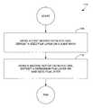
- FIG. 1is a diagrammatic flow chart illustrating a chemical vapor deposition method according to a preferred embodiment of the present invention
- FIG. 2is a photo of an a silicon substrate, with no seed layer, which has been subjected to a chemical vapor deposition process using a catalytic gas of GeH 4 at an elevated temperature of about 400° Celsius;
- FIG. 3is a photo of an a silicon substrate after being subjected to the chemical vapor deposition process mentioned relative to FIG. 2 ;
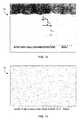
- FIG. 4is an x-ray diffraction graph illustrating that the deposited germanium film layer as shown in FIG. 2 is polycrystalline;
- FIG. 5is a photo of an a silicon substrate, which has been subjected to a chemical vapor deposition process at an elevated temperature of about 380° Celsius;
- FIG. 6is a photo of an a silicon substrate after being subjected to the chemical vapor deposition process mentioned relative to FIG. 5 ;
- FIG. 7is a photo of a silicon dioxide substrate, which has been subjected to a chemical vapor deposition process at an elevated temperature of about 380° Celsius;
- FIG. 8is a photo of a silicon dioxide substrate after being subjected to the chemical vapor deposition process mentioned relative to FIG. 7 ;
- FIG. 9is a photo of an a silicon substrate, which has been subjected to a chemical vapor deposition process at an elevated temperature of about 380° Celsius;
- FIG. 10is a photo of an a silicon substrate, which has been subjected to a chemical vapor deposition process mentioned relative to FIG. 9 ;
- FIG. 11is a photo of a silicon dioxide, which has been subjected to a chemical vapor deposition process at an elevated temperature of about 380° Celsius;
- FIG. 12is photo of a TiN substrate, which has been subjected to a chemical vapor deposition process at an elevated temperature of about 380° C.;
- FIG. 13is a photo of an a silicon substrate, which has been subjected to a chemical vapor deposition process at an elevated temperature of about 360° Celsius;
- FIG. 14is a photo of an a silicon substrate, which has been subjected to the chemical vapor deposition process mentioned relative to FIG. 13 ;
- FIG. 15is a photo of a silicon dioxide substrate, which has been subjected to a chemical vapor deposition process at an elevated temperature of about 360° C.;
- FIG. 16is a photo of a TiN substrate, which has been subjected to a chemical vapor deposition process at an elevated temperature of about 360° C.;
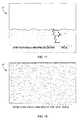
- FIG. 17is a photo of an a silicon substrate, which has been subjected to a chemical vapor deposition process at an elevated temperature of about 340° C.;
- FIG. 18is a photo of an a silicon substrate, which has been subjected to the chemical vapor deposition process mentioned relative to FIG. 17 ;
- FIG. 19is a photo of a TiN substrate, which has been subjected to a chemical vapor deposition process at an elevated temperature of about 340° C.;
- FIG. 20is a photo of an a silicon substrate, which has been subjected to a chemical vapor deposition process at an elevated temperature of about 320° C.;
- FIG. 21is a photo of an a silicon substrate, which has been subjected to the chemical vapor process mentioned relative to FIG. 20 ;
- FIG. 22is a photo of a TiN substrate, which has been subjected to a chemical vapor deposition process at an elevated temperature of about 320° C.;
- FIG. 23is a photo of a TiN substrate, which has been subjected to the chemical vapor deposition process mentioned relative to FIG. 22 ;
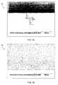
- FIG. 24is a photo of a TiN substrate, which has been subjected to a chemical vapor deposition process in accordance with a preferred embodiment of the present invention.
- FIG. 25is a photo of a TiN substrate, which has been subjected to the chemical vapor deposition process mentioned relative to FIG. 24 .
- FIG. 1there is shown a flow chart of a chemical vapor deposition method 112 , which is in accordance with a preferred embodiment of the present invention.
- the disclosed method 112enables the deposition of amorphous or polycrystalline germanium or silicon germanium homogenous films on silicon dioxide and metallic substrates at very low temperature of less than 320° C. by chemical vapor deposition.
- this methodapplies to semiconductor devices, for example, for use in making memory devices, such as set forth in U.S. Patent Application Publication 20050012119, entitled, “Method for Making High Density Nonvolatile Memory,”by S. B. Herner and M. Mahajani.
- germanium and silicon germaniumhereinafter individually and collectively sometimes referred to as simply Ge films
- the standard method for depositing Ge films by chemical vapor deposition on a silicon dioxide substrateis to first deposit a thin silicon film as a seed layer.
- the silicon film seed layeris deposited to a predetermined minimized thickness to help minimize the impact on the electrical properties of the combined silicon and germanium or the combined silicon and silicon germanium film.
- the Ge film layeris then deposited at an elevated temperature of something greater than 450° Celsius by chemical vapor deposition (CVD).
- CVDchemical vapor deposition
- the CVD method of depositing germanium using a GeH 4 precursor gashowever has a disadvantage. That is, Ge films can have either a large incubation time (or time-to-initiate deposition) leaving the final film as heterogeneous or lumpy; or the Ge will not deposit at all on some substrates. This is caused by the difficulty of “cracking” the GeH 4 molecule to deposit germanium and remove hydrogen on some substrates. In this regard, it has been shown that it is difficult to deposit germanium (by GeH 4 catalysis) on SiO 2 substrates, while it is easier to deposit on silicon substrates.
- silicon germanium deposition on a silicon dioxide substrateis well known in the art.
- the method of using a silicon “seed” layer on a silicon dioxide substrate to help facilitate the silicon germanium depositis well known.
- these silicon seed layer depositionsare all performed at elevated temperature of greater than 500° Celsius, when using SiH 4 as a source for Si.
- the processbegins at a using step 114 , which causes a first catalytic gas source, such as a silicon gas source, to flow across a substrate, such as a metallic substrate for the purpose of depositing a seed film of silicon on the substrate.
- a using step 116causes a second catalytic gas source, such as a germanium gas source, to flow across the seeded substrate for the purpose of depositing a germanium film on the seed layer of silicon.
- a first catalytic gas sourcesuch as a silicon gas source
- a substratesuch as a metallic substrate for the purpose of depositing a seed film of silicon on the substrate.
- a using step 116causes a second catalytic gas source, such as a germanium gas source, to flow across the seeded substrate for the purpose of depositing a germanium film on the seed layer of silicon.
- the seed layer of siliconis a self-limited seed layer. This means that the reaction proceeds to deposit silicon until full coverage of the exposed underlying layer is achieved.
- the metallic substrate with the film layers deposited thereonare suitable for use with other temperature sensitive materials that would otherwise be precluded by higher temperature deposition of germanium or silicon-germanium by other methods.
- the self-limited silicon seed layeris formed using an inexpensive, widely available precursor gas, enabling Ge deposition on the substrate at much lower temperatures ( ⁇ 320° C.) than known in the prior art.
- Such low temperature depositionin turn, enables the use of thermally sensitive materials, such as aluminum wiring, chalcogenide memory materials, and copper as examples, that would be precluded by higher temperature Si or SiGe deposition (>475° C.).
- the self-limited featurealso minimizes the Si deposition, therefore, minimizing Si impact on the resulting device, which is desirable.
- the deposition method 112enables integration with other temperature sensitive materials, such as Aluminum (Al) and Copper (Cu) wiring. Also the method 112 , utilizes a lower temperature SiH 4 catalysis for “cracking on Titanium nitride (TiN) to produce a self limited ⁇ layer of silicon ( ⁇ 4 ⁇ ).
- TiNTitanium nitride
- the use of such a seed layer for a Ge film depositionis unique and novel. Moreover, minimizing the thickness of the silicon seed is very advantageous, and self-limitation is inherently more manufacturable since it is subject to less operator errors.
- the deposition method 112provides a novel process for deposition of Ge films on, for example, TiN or SiO 2 substrates at temperatures below 330° Celsius.
- the Ge filmis crystallized in a subsequent step. Crystallization of the Ge film takes place at a temperature of between about 350° C. and about 425° C.
- Ge semiconductor devicescan be integrated with other thermally sensitive materials, such as aluminum interconnect or chalcogenides memory materials. It should be recognized however, by those skilled in the art, that this does not preclude the use of the Ge film as a semiconductor in its amorphous state.
- FIGS. 2-3 and FIGS. 5-23a series of scanning electronic microscope (SEM) photographs or images are provided ( FIGS. 2-3 and FIGS. 5-23 ).
- SEMscanning electronic microscope
- the silicon seed layeris not visible.
- the inventive process 112as illustrated in FIGS. 24-25 , a SiO 2 layer C 24 and a Ge film layer A 24 are deposited in one deposition (two steps). It should be noted that a Si seed layer exists between the Ge film A 24 and the TiN film B 24 but the Si seed layer is not visible.
- FIGS. 2 and 3there is provided a set of scanning electronic microscope photographs that illustrate the results of a germanium deposition at 400° Celsius, utilizing a 100 standard cubic centimeter per minute flow rate of GeH 4 gas, delivered at a pressure of 100 mTorr, for a 30 minute period on a 220 nanometer a silicon substrate 12 with no seed layer.
- a resulting germanium film layer A 2with a depth of about 0.1480 ⁇ m
- a separately deposited silicon film layer B 2with a depth of about 0.2180 ⁇ m of doped and undoped silicon, which has been deposited on a layer C 2 of silicon dioxide, has a depth of about 0.0910 ⁇ m.
- FIG. 1As best seen in FIG.
- an x-ray diffraction graph 412clearly confirms that the deposited Ge film is polycrystalline. It was also determined by SEM imaging, although not shown in separate photographs, that with both a SiO 2 substrate and a TiN substrate, no deposition occurred relative to the condition mentioned.
- FIGS. 5-6there is provided a set of photographs which illustrate the results of a germanium deposition at 380° Celsius, utilizing a 500 standard cubic centimeter per minute flow rate of SiH 4 gas, delivered at a pressure of 400 mTorr, for a 60 minute period on an a silicon substrate 15 .
- a resulting germanium film layer A 5with a depth of about 0.0750 ⁇ m
- a separately deposited silicon film layer B 5with a depth of about 0.1510 ⁇ m, which has been deposited on a silicon dioxide layer C 5 having a depth of about 0.0950 ⁇ m.
- FIGS. 7-8there is provided a set of photographs which illustrates the results of a germanium deposition at 380° C., utilizing a 100 standard cubic centimeter per minute flow rate of GeH 4 gas, delivered at a pressure of 200 mTorr, for a 10 minute period on a silicon dioxide substrate 17 .
- a resulting germanium film layer A 7 with a depth of about 0.0930 ⁇ ma separately deposited SiO 2 film layer B 7 with a depth of about 0.0930 ⁇ m. It was also determined by SEM imaging, although not shown in a separate photograph, that with a TiN substrate, no deposition occurred relative to the condition mentioned.
- FIGS. 9-10there is provided a set of photographs which illustrates the results of a germanium deposition at 380° Celsius, utilizing a 500 standard cubic centimeter per minute flow rate of SiH 4 gas, delivered at a pressure of 800 mTorr, for a 60 minute period on an a silicon substrate 19 .
- a resulting germanium film layer A 9with a depth of about 0.0570 ⁇ m
- a resulting silicon film layer B 9with a depth of about 0.0530 ⁇ m. which is deposited on a silicon diode layer C 9 with a depth of about 0.1000 ⁇ m.
- FIG. 11there is provided a photograph which illustrates the results of a germanium deposition at 380° Celsius., utilizing a 100 standard cubic centimeter per minute flow rate of GeH 4 gas, delivered at a pressure of 400 mTorr, for a 10 minute period on a SiO 2 substrate 21 .
- FIG. 12there is provided a photograph which illustrates the results of a germanium deposition at 380° Celsius, utilizing a 100 standard cubic centimeter per minute flow rate of GeH 4 gas, delivered at a pressure of 400 mTorr, for a 10 minute period on a TiN substrate 22 .
- a resulting germanium film layer A 12 with a depth of about 0.0860 ⁇ mthere is shown a resulting TiN film layer B 12 with a depth of about 0.0290 ⁇ m, which has been deposited on a silicon dioxide layer C 12 with a depth of about 0.0900 ⁇ m.
- FIGS. 13-14there is provided a set of photographs which illustrate the results of a germanium deposition at 360 ° Celsius, utilizing a 500 standard cubic centimeter per minute flow rate of SiH 4 gas, delivered at a pressure of 800 mTorr, for a 60 minute period on an a silicon substrate 23 .
- a resulting silicon film layer B 13 with a depth of about 0.0600 ⁇ mwhich has been deposited on a silicon dioxide layer C 13 with a depth of about 0.0990 ⁇ m.
- FIG. 15there is provided a photograph which illustrates the results of a germanium deposition at 360° Celsius, utilizing a 100 standard cubic centimeter per minute flow rate of GeH 4 gas, delivered at a pressure of 400 mTorr, for a 10 minute period on a SiO 2 substrate 25 .
- FIG. 16there is provided a photograph which illustrates the results of a germanium deposition at 360° Celsius, utilizing a 100 standard cubic centimeter per minute flow rate of GeH 4 gas, delivered at a pressure of 400 mTorr, for a 10 minute period on a TiN substrate 26 .
- a resulting germanium film layer A 16 with a depth of about 0.0470 ⁇ mthere is shown a resulting TiN film layer B 16 with a depth of about 0.0300 ⁇ m, which has been deposited on a silicon dioxide layer C 16 with a depth of about 0.0860 ⁇ m.
- FIGS. 17-18there is provided a set of photographs which illustrate the results of a germanium deposition at 340° Celsius, utilizing a 500 standard cubic centimeter per minute flow rate of SiH 4 gas, delivered at a pressure of 800 mTorr, for a 60 minute period on an a silicon substrate 27 .
- a resulting germanium film layer A 17 with a depth of about 0.0400 ⁇ ma separately deposited silicon film layer B 17 with a depth of about 0.0260 ⁇ m, which has been deposited on a silicon dioxide layer C 17 with a depth of about 0.0930 ⁇ m.
- This processresults in a Ge film deposit rate of about 40 ⁇ per minute.
- FIG. 19there is provided a photograph which illustrates the results of a germanium deposition at 340° Celsius, utilizing a 100 standard cubic centimeter per minute flow rate of GeH 4 gas, delivered at a pressure of 800 mTorr, for a 10 minute period on a TiN substrate 29 .
- a resulting germanium film layer A 19 with a depth of about 0.0700 ⁇ ma resulting TiN film layer B 19 with a depth of about 0.0380 ⁇ m, which has been deposited on a silicon dioxide layer C 19 with a depth of about 0.1010 ⁇ m.
- This processresults in a Ge film deposit rate of about 70 ⁇ per minute. It was also determined by SEM imaging, although not shown in a separate photograph, that with a SiO 2 substrate, no deposition occurred relative to the condition mentioned.
- FIGS. 20-21there is provided a set of photographs which illustrates the results of a germanium deposition at 320° Celsius, utilizing a 500 standard cubic centimeter per minute flow rate of SiH 4 gas, delivered at a pressure of 1000 mTorr, for a 60 minute period on an a silicon substrate 30 .
- FIGS. 22-23there is provided a set of photographs which illustrates the results of a germanium deposition at 320° Celsius, utilizing a 100 standard cubic centimeter per minute flow rate of GeH 4 gas, delivered at a pressure of 1000 mTorr, for a 20 minute period on a TiN substrate 32 .
- a resulting germanium film layer A 22 with a depth of about 0.0640 ⁇ ma resulting TiN film layer B 22 with a depth of about 0.0270 ⁇ m, which has been deposited on a silicon dioxide layer C 22 with a depth of about 0.0930 ⁇ m.
- This processresults in a Ge film deposition rate of about 32 ⁇ per minute.
- FIGS. 20-22it can be seen that the Ge film deposition is now amorphous, but the deposition appears somewhat irregular on the TiN substrate 32 .
- FIGS. 24-25there is provided a set of photographs, which illustrate the results of a germanium deposition using a combined 380° Celsius and 320° Celsius process.
- a seed layer of silicon C 24is deposited at 380° Celsius, utilizing a 500 standard cubic centimeter per minute flow rate of SiH 4 gas, delivered at a pressure of 1000 mTorr, for a 60 minute period on a TiN substrate 34 .
- a Ge film layer A 24is deposited at 320° Celsius, utilizing a 200 standard cubic centimeter per minute flow rate of GeH 4 gas, delivered at a pressure of 1000 mTorr, for a 20-minute period.
- a resulting Ge film layer A 24 with a depth of about 0.0640 ⁇ ma resulting TiN film layer B 24 with a depth of about 0.0270 ⁇ m, which has been deposited on a silicon dioxide layer C 24 with a depth of about 0.0930 ⁇ m.
- a smooth continuous filmresults with a two-temperature process (one deposition), where the applied temperatures are sufficiently low (320° Celsius or less) to be completely compatible with Al, Cu wiring or GST material. It can also be concluded that SiH 4 gas will decompose on TiN more readily at these lower temperatures than on silicon or on silicon dioxide substrates. Finally, once the silicon layer is deposited, the SiH 4 gas will no longer decompose resulting in a self-limited process. This self-limited feature minimizes silicon deposition and therefore minimizes the silicon impact on the resulting Ge or SiGe device, which is very desirable. Most importantly, this self-limited process is accomplished without the use of special gases and instead utilizes readily available gases for Si, Ge, and SiGe depositions.
- dislaneSi 2 H 6
- tri silaneSi 3 H 8
- Ge gas sourcescould also be utilized like, GeF 4 , GeBr 4 , or GeCl 4 .
Landscapes
- Chemical & Material Sciences (AREA)
- General Chemical & Material Sciences (AREA)
- Chemical Kinetics & Catalysis (AREA)
- Engineering & Computer Science (AREA)
- Materials Engineering (AREA)
- Mechanical Engineering (AREA)
- Metallurgy (AREA)
- Organic Chemistry (AREA)
- Inorganic Chemistry (AREA)
- Chemical Vapour Deposition (AREA)
Abstract
Description
- It is well known to those skilled in the art that the deposition of germanium or silicon germanium by chemical vapor deposition is extremely sensitive relative to a receiving substrate. For example, germanium or silicon germanium deposition on a silicon substrate is relatively easy. On the other hand, germanium or silicon germanium deposition, heretofore, on silicon dioxide or metallic substrates has either required an extremely large incubation time (time-to-initiate deposition) with a resultant heterogeneous or lumpy deposition or would not deposit at all on some substrates at temperatures below 450° Celsius. Therefore it would be highly desirable to have a new and improved method of depositing amorphous germanium films on metallic or silicon dioxide substrates at temperatures less than 450° Celsius.
- In one preferred chemical vapor deposition method, a smooth continuous germanium film is deposited on a silicon seeded metallic substrate at a sufficiently low temperature to provide a germanium device suitable for integration with temperature sensitive materials such as aluminum and copper. In another preferred chemical vapor deposition method, a smooth continuous silicon germanium film is deposited on a seeded silicon dioxide substrate at a sufficiently low temperature to provide a germanium device suitable for use with temperature sensitive materials such as aluminum, copper and chalcogenides, such as Ge2Sb2Te5=l .
- The above mentioned features and steps of the invention and the manner of attaining them will become apparent, and the invention itself will be best understood by reference to the following description of the preferred embodiment(s) of the invention in conjunction with the accompanying drawings wherein:
FIG. 1 is a diagrammatic flow chart illustrating a chemical vapor deposition method according to a preferred embodiment of the present invention;FIG. 2 is a photo of an a silicon substrate, with no seed layer, which has been subjected to a chemical vapor deposition process using a catalytic gas of GeH4at an elevated temperature of about 400° Celsius;FIG. 3 is a photo of an a silicon substrate after being subjected to the chemical vapor deposition process mentioned relative toFIG. 2 ;FIG. 4 is an x-ray diffraction graph illustrating that the deposited germanium film layer as shown inFIG. 2 is polycrystalline;FIG. 5 is a photo of an a silicon substrate, which has been subjected to a chemical vapor deposition process at an elevated temperature of about 380° Celsius;FIG. 6 is a photo of an a silicon substrate after being subjected to the chemical vapor deposition process mentioned relative toFIG. 5 ;FIG. 7 is a photo of a silicon dioxide substrate, which has been subjected to a chemical vapor deposition process at an elevated temperature of about 380° Celsius;FIG. 8 is a photo of a silicon dioxide substrate after being subjected to the chemical vapor deposition process mentioned relative toFIG. 7 ;FIG. 9 is a photo of an a silicon substrate, which has been subjected to a chemical vapor deposition process at an elevated temperature of about 380° Celsius;FIG. 10 is a photo of an a silicon substrate, which has been subjected to a chemical vapor deposition process mentioned relative toFIG. 9 ;FIG. 11 is a photo of a silicon dioxide, which has been subjected to a chemical vapor deposition process at an elevated temperature of about 380° Celsius;FIG. 12 is photo of a TiN substrate, which has been subjected to a chemical vapor deposition process at an elevated temperature of about 380° C.;- FIG.13 is a photo of an a silicon substrate, which has been subjected to a chemical vapor deposition process at an elevated temperature of about 360° Celsius;
FIG. 14 is a photo of an a silicon substrate, which has been subjected to the chemical vapor deposition process mentioned relative toFIG. 13 ;FIG. 15 is a photo of a silicon dioxide substrate, which has been subjected to a chemical vapor deposition process at an elevated temperature of about 360° C.;FIG. 16 is a photo of a TiN substrate, which has been subjected to a chemical vapor deposition process at an elevated temperature of about 360° C.;FIG. 17 is a photo of an a silicon substrate, which has been subjected to a chemical vapor deposition process at an elevated temperature of about 340° C.;FIG. 18 is a photo of an a silicon substrate, which has been subjected to the chemical vapor deposition process mentioned relative toFIG. 17 ;FIG. 19 is a photo of a TiN substrate, which has been subjected to a chemical vapor deposition process at an elevated temperature of about 340° C.;FIG. 20 is a photo of an a silicon substrate, which has been subjected to a chemical vapor deposition process at an elevated temperature of about 320° C.;FIG. 21 is a photo of an a silicon substrate, which has been subjected to the chemical vapor process mentioned relative toFIG. 20 ;FIG. 22 is a photo of a TiN substrate, which has been subjected to a chemical vapor deposition process at an elevated temperature of about 320° C.;FIG. 23 is a photo of a TiN substrate, which has been subjected to the chemical vapor deposition process mentioned relative toFIG. 22 ;FIG. 24 is a photo of a TiN substrate, which has been subjected to a chemical vapor deposition process in accordance with a preferred embodiment of the present invention; andFIG. 25 is a photo of a TiN substrate, which has been subjected to the chemical vapor deposition process mentioned relative toFIG. 24 .- A method of germanium film deposition on metallic and silicon dioxide substrates is disclosed. The following description is presented to enable any person skilled in the art to make and use the invention. For purposes of explanation, specific nomenclature is set forth to provide a thorough understanding of the present invention. Descriptions of specific applications, and methods are provided only as examples. Various modifications to the preferred embodiments will be readily apparent to those skilled in the art, and the general principles defined herein may be applied to other embodiments and applications without departing from the spirit and scope of the invention. Thus, the present invention is not intended to be limited to the embodiments shown, but is to be accorded the widest scope consistent with the principles and steps disclosed herein.
- Referring now to the drawings and more particularly to
FIG. 1 thereof, there is shown a flow chart of a chemicalvapor deposition method 112, which is in accordance with a preferred embodiment of the present invention. The disclosedmethod 112 enables the deposition of amorphous or polycrystalline germanium or silicon germanium homogenous films on silicon dioxide and metallic substrates at very low temperature of less than 320° C. by chemical vapor deposition. In this regard, this method applies to semiconductor devices, for example, for use in making memory devices, such as set forth in U.S. Patent Application Publication 20050012119, entitled, “Method for Making High Density Nonvolatile Memory,”by S. B. Herner and M. Mahajani. - Before discussing the
deposition method 112 in greater detail, it may be beneficial to briefly review the current state of the art for depositing germanium and silicon germanium (hereinafter individually and collectively sometimes referred to as simply Ge films) on dioxide or metallic substrates. In this regard, the standard method for depositing Ge films by chemical vapor deposition on a silicon dioxide substrate is to first deposit a thin silicon film as a seed layer. The silicon film seed layer is deposited to a predetermined minimized thickness to help minimize the impact on the electrical properties of the combined silicon and germanium or the combined silicon and silicon germanium film. - After deposition of the silicon seed layer, the Ge film layer is then deposited at an elevated temperature of something greater than 450° Celsius by chemical vapor deposition (CVD). The CVD method of depositing germanium using a GeH4precursor gas however has a disadvantage. That is, Ge films can have either a large incubation time (or time-to-initiate deposition) leaving the final film as heterogeneous or lumpy; or the Ge will not deposit at all on some substrates. This is caused by the difficulty of “cracking” the GeH4molecule to deposit germanium and remove hydrogen on some substrates. In this regard, it has been shown that it is difficult to deposit germanium (by GeH4catalysis) on SiO2substrates, while it is easier to deposit on silicon substrates.
- The difficulty in silicon germanium deposition on a silicon dioxide substrate is well known in the art. Also, the method of using a silicon “seed” layer on a silicon dioxide substrate to help facilitate the silicon germanium deposit is well known. However, these silicon seed layer depositions are all performed at elevated temperature of greater than 500° Celsius, when using SiH4as a source for Si. For example, reference may be made to the following publication which is incorporated herein as though fully set forth: “Low Pressure Chemical Vapor Deposition of Si1-xGexFilms On SiO2,” by M. Cao, A. Wang, K. C. Saraswat, Journal of the Electrochemical Society 142, 1566-1572 (1995).
- Considering now the
deposition method 112 in greater detail with reference toFIG. 1 , the process begins at a usingstep 114, which causes a first catalytic gas source, such as a silicon gas source, to flow across a substrate, such as a metallic substrate for the purpose of depositing a seed film of silicon on the substrate. Next, a usingstep 116 causes a second catalytic gas source, such as a germanium gas source, to flow across the seeded substrate for the purpose of depositing a germanium film on the seed layer of silicon. As will be explained hereinafter in greater detail, because of the type of silicon gas employed and temperature used, the seed layer of silicon is a self-limited seed layer. This means that the reaction proceeds to deposit silicon until full coverage of the exposed underlying layer is achieved. This results in a thin layer, for example, which could be one to three atoms in thickness. Moreover, because the second catalytic gas is delivered at a sufficiently low temperature (320° C. or lower) the metallic substrate with the film layers deposited thereon, are suitable for use with other temperature sensitive materials that would otherwise be precluded by higher temperature deposition of germanium or silicon-germanium by other methods. - In short then, the self-limited silicon seed layer is formed using an inexpensive, widely available precursor gas, enabling Ge deposition on the substrate at much lower temperatures (<320° C.) than known in the prior art. Such low temperature deposition in turn, enables the use of thermally sensitive materials, such as aluminum wiring, chalcogenide memory materials, and copper as examples, that would be precluded by higher temperature Si or SiGe deposition (>475° C.). The self-limited feature also minimizes the Si deposition, therefore, minimizing Si impact on the resulting device, which is desirable. Finally, all of these advantages, over the prior art, are accomplished without the use of special expensive gases.
- Considering now the
deposition method 112 in still greater detail, the deposition method of depositing Ge films on metallic and dioxide substrates enables integration with other temperature sensitive materials, such as Aluminum (Al) and Copper (Cu) wiring. Also themethod 112, utilizes a lower temperature SiH4catalysis for “cracking on Titanium nitride (TiN) to produce a self limited ˜layer of silicon (˜4 Å). The use of such a seed layer for a Ge film deposition is unique and novel. Moreover, minimizing the thickness of the silicon seed is very advantageous, and self-limitation is inherently more manufacturable since it is subject to less operator errors. - The
deposition method 112, as will be explained hereinafter in greater detail, provides a novel process for deposition of Ge films on, for example, TiN or SiO2substrates at temperatures below 330° Celsius. After deposition of the amorphous Ge film at 330° C. (or less), the Ge film is crystallized in a subsequent step. Crystallization of the Ge film takes place at a temperature of between about 350° C. and about 425° C. By depositing the film amorphous and then, at a later step, heating the amorphous Ge film for a sufficient period of time to cause the film to crystallize so that crystallized semiconductor device performance is improved compared to depositing the film crystalline. By keeping the temperature at 420° C. or less for Ge processing, Ge semiconductor devices can be integrated with other thermally sensitive materials, such as aluminum interconnect or chalcogenides memory materials. It should be recognized however, by those skilled in the art, that this does not preclude the use of the Ge film as a semiconductor in its amorphous state. - In order to provide the reader with a better understanding of the benefits derived from the inventive chemical vapor disposition process, a series of scanning electronic microscope (SEM) photographs or images are provided (
FIGS. 2-3 andFIGS. 5-23 ). In each of the SEM photographs, the silicon seed layer is not visible. In this regard, when a silicon film is indicated, the silicon film has been deposited in a separate deposition. In theinventive process 112, as illustrated inFIGS. 24-25 , a SiO2layer C24and a Ge film layer A24are deposited in one deposition (two steps). It should be noted that a Si seed layer exists between the Ge film A24and the TiN film B24but the Si seed layer is not visible. - Referring now to
FIGS. 2 and 3 , there is provided a set of scanning electronic microscope photographs that illustrate the results of a germanium deposition at 400° Celsius, utilizing a 100 standard cubic centimeter per minute flow rate of GeH4gas, delivered at a pressure of 100 mTorr, for a 30 minute period on a 220 nanometer asilicon substrate 12 with no seed layer. In this regard, there is shown a resulting germanium film layer A2with a depth of about 0.1480 μm, a separately deposited silicon film layer B2with a depth of about 0.2180 μm of doped and undoped silicon, which has been deposited on a layer C2of silicon dioxide, has a depth of about 0.0910 μm. As best seen inFIG. 4 , anx-ray diffraction graph 412, clearly confirms that the deposited Ge film is polycrystalline. It was also determined by SEM imaging, although not shown in separate photographs, that with both a SiO2substrate and a TiN substrate, no deposition occurred relative to the condition mentioned. - Referring now to
FIGS. 5-6 , there is provided a set of photographs which illustrate the results of a germanium deposition at 380° Celsius, utilizing a 500 standard cubic centimeter per minute flow rate of SiH4gas, delivered at a pressure of 400 mTorr, for a 60 minute period on an asilicon substrate 15. In this regard, there is shown a resulting germanium film layer A5with a depth of about 0.0750 μm, a separately deposited silicon film layer B5with a depth of about 0.1510 μm, which has been deposited on a silicon dioxide layer C5having a depth of about 0.0950 μm. - Referring now to
FIGS. 7-8 , there is provided a set of photographs which illustrates the results of a germanium deposition at 380° C., utilizing a 100 standard cubic centimeter per minute flow rate of GeH4gas, delivered at a pressure of 200 mTorr, for a 10 minute period on asilicon dioxide substrate 17. In this regard, there is shown a resulting germanium film layer A7with a depth of about 0.0930 μm, a separately deposited SiO2film layer B7with a depth of about 0.0930 μm. It was also determined by SEM imaging, although not shown in a separate photograph, that with a TiN substrate, no deposition occurred relative to the condition mentioned. - Referring now to
FIGS. 9-10 , there is provided a set of photographs which illustrates the results of a germanium deposition at 380° Celsius, utilizing a 500 standard cubic centimeter per minute flow rate of SiH4gas, delivered at a pressure of 800 mTorr, for a 60 minute period on an asilicon substrate 19. In this regard, there is shown a resulting germanium film layer A9with a depth of about 0.0570 μm, a resulting silicon film layer B9with a depth of about 0.0530 μm. which is deposited on a silicon diode layer C9with a depth of about 0.1000 μm. - Referring now to
FIG. 11 , there is provided a photograph which illustrates the results of a germanium deposition at 380° Celsius., utilizing a 100 standard cubic centimeter per minute flow rate of GeH4gas, delivered at a pressure of 400 mTorr, for a 10 minute period on a SiO2substrate21. In this regard, there is shown a resulting germanium film layer A11with a depth of about 0.0730 μm, and a resulting SiO2film layer B11with a depth of about 0.0880 μm, on the SiO2substrate layer21. - Referring now to
FIG. 12 , there is provided a photograph which illustrates the results of a germanium deposition at 380° Celsius, utilizing a 100 standard cubic centimeter per minute flow rate of GeH4gas, delivered at a pressure of 400 mTorr, for a 10 minute period on aTiN substrate 22. In this regard, there is shown a resulting germanium film layer A12with a depth of about 0.0860 μm, and a resulting TiN film layer B12with a depth of about 0.0290 μm, which has been deposited on a silicon dioxide layer C12with a depth of about 0.0900 μm. - With respect to
FIGS. 9-12 it can be seen that the increased pressure during the silicon-seeding phase better enabled Ge deposition on both the SiO2substrate19 and theTiN substrate 22. - Referring now to
FIGS. 13-14 , there is provided a set of photographs which illustrate the results of a germanium deposition at360° Celsius, utilizing a 500 standard cubic centimeter per minute flow rate of SiH4gas, delivered at a pressure of 800 mTorr, for a 60 minute period on an asilicon substrate 23. In this regard, there is shown a resulting germanium film layer A13with a depth of about 0.0400 μm, a resulting silicon film layer B13with a depth of about 0.0600 μm, which has been deposited on a silicon dioxide layer C13with a depth of about 0.0990 μm. - Referring now to
FIG. 15 , there is provided a photograph which illustrates the results of a germanium deposition at 360° Celsius, utilizing a 100 standard cubic centimeter per minute flow rate of GeH4gas, delivered at a pressure of 400 mTorr, for a 10 minute period on a SiO2substrate25. In this regard, there is shown a resulting germanium film layer A15with a depth of about 0.0410 μm, and a resulting SiO2film layer B15with a depth of about 0.0930 μm, on the SiO2substrate layer25. - Referring now to
FIG. 16 , there is provided a photograph which illustrates the results of a germanium deposition at 360° Celsius, utilizing a 100 standard cubic centimeter per minute flow rate of GeH4gas, delivered at a pressure of 400 mTorr, for a 10 minute period on aTiN substrate 26. In this regard, there is shown a resulting germanium film layer A16with a depth of about 0.0470 μm, and a resulting TiN film layer B16with a depth of about 0.0300 μm, which has been deposited on a silicon dioxide layer C16with a depth of about 0.0860 μm. - With respect to
FIGS. 13-16 it can be seen that the decrease in temperature degraded the Ge film deposition on the SiO2substrate since the SiH4decomposition is most likely becoming less effective at providing a seed layer that fully covers the substrate at the lower temperature. It can also be seen that the Ge films are poly-crystalline so there is a need to further decrease the deposition to have a resulting amorphous Ge film. - Referring now to
FIGS. 17-18 , there is provided a set of photographs which illustrate the results of a germanium deposition at 340° Celsius, utilizing a 500 standard cubic centimeter per minute flow rate of SiH4gas, delivered at a pressure of 800 mTorr, for a 60 minute period on an asilicon substrate 27. In this regard, there is shown a resulting germanium film layer A17with a depth of about 0.0400 μm, a separately deposited silicon film layer B17with a depth of about 0.0260 μm, which has been deposited on a silicon dioxide layer C17with a depth of about 0.0930 μm. This process results in a Ge film deposit rate of about 40 Åper minute. - Referring now to
FIG. 19 , there is provided a photograph which illustrates the results of a germanium deposition at 340° Celsius, utilizing a 100 standard cubic centimeter per minute flow rate of GeH4gas, delivered at a pressure of 800 mTorr, for a 10 minute period on aTiN substrate 29. In this regard, there is shown a resulting germanium film layer A19with a depth of about 0.0700 μm, a resulting TiN film layer B19with a depth of about 0.0380 μm, which has been deposited on a silicon dioxide layer C19with a depth of about 0.1010 μm. This process results in a Ge film deposit rate of about 70 Å per minute. It was also determined by SEM imaging, although not shown in a separate photograph, that with a SiO2substrate, no deposition occurred relative to the condition mentioned. - With respect to
FIGS. 17-19 it can be seen that the decrease in temperature has now completely failed to deposit a Ge film the SiO2substrate. Moreover, even the Ge film deposition on the TiN substrate has degraded. It can also be seen that the silicon film and the germanium film are still polycrystalline, so there is still a need to further decrease the deposition to have a resulting amorphous Ge film. - Referring now to
FIGS. 20-21 , there is provided a set of photographs which illustrates the results of a germanium deposition at 320° Celsius, utilizing a 500 standard cubic centimeter per minute flow rate of SiH4gas, delivered at a pressure of 1000 mTorr, for a 60 minute period on an asilicon substrate 30. In this regard, there is shown a resulting germanium film layer A20with a depth of about 0.1280 μm, and a separately deposited silicon film layer B20with a depth of about 0.0980 μm, on the TiN substrate layer. - Referring now to
FIGS. 22-23 , there is provided a set of photographs which illustrates the results of a germanium deposition at 320° Celsius, utilizing a 100 standard cubic centimeter per minute flow rate of GeH4gas, delivered at a pressure of 1000 mTorr, for a 20 minute period on aTiN substrate 32. In this regard, there is shown a resulting germanium film layer A22with a depth of about 0.0640 μm, a resulting TiN film layer B22with a depth of about 0.0270 μm, which has been deposited on a silicon dioxide layer C22with a depth of about 0.0930 μm. This process results in a Ge film deposition rate of about 32 Åper minute. Also with respect toFIGS. 20-22 it can be seen that the Ge film deposition is now amorphous, but the deposition appears somewhat irregular on theTiN substrate 32. - Referring now to
FIGS. 24-25 , there is provided a set of photographs, which illustrate the results of a germanium deposition using a combined 380° Celsius and 320° Celsius process. In the regard, a seed layer of silicon C24is deposited at 380° Celsius, utilizing a 500 standard cubic centimeter per minute flow rate of SiH4gas, delivered at a pressure of 1000 mTorr, for a 60 minute period on aTiN substrate 34. Next, a Ge film layer A24is deposited at 320° Celsius, utilizing a 200 standard cubic centimeter per minute flow rate of GeH4gas, delivered at a pressure of 1000 mTorr, for a 20-minute period. In this regard, there is shown a resulting Ge film layer A24with a depth of about 0.0640 μm, a resulting TiN film layer B24with a depth of about 0.0270 μm, which has been deposited on a silicon dioxide layer C24with a depth of about 0.0930 μm. - In summary then, a smooth continuous film results with a two-temperature process (one deposition), where the applied temperatures are sufficiently low (320° Celsius or less) to be completely compatible with Al, Cu wiring or GST material. It can also be concluded that SiH4gas will decompose on TiN more readily at these lower temperatures than on silicon or on silicon dioxide substrates. Finally, once the silicon layer is deposited, the SiH4gas will no longer decompose resulting in a self-limited process. This self-limited feature minimizes silicon deposition and therefore minimizes the silicon impact on the resulting Ge or SiGe device, which is very desirable. Most importantly, this self-limited process is accomplished without the use of special gases and instead utilizes readily available gases for Si, Ge, and SiGe depositions.
- While a particular embodiment of the present invention has been disclosed, it is to be understood that various different modifications are possible and are contemplated within the true spirit and scope of the appended claims. For example, while the effect has been demonstrated for TiN substrates it is fully expected that the effect will be useful on other metallic substrates such as Ta, TaN, W and WN, as well as other silicon type substrates, such as SiO2, SiN and SiNxsubstrates. Also although the use of a common source catalytic gas source, such as SiH4gas, has been described relative to the preferred embodiment, it is contemplated that more expensive Si gas sources that decompose for depositing a Si seed layers at lower temperatures could also be utilized. For example, dislane (Si2H6) and tri silane (Si3H8) could be utilized. Similarly alternative Ge gas sources could also be utilized like, GeF4, GeBr4, or GeCl4. There is no intention, therefore, of limitations to the exact abstract or disclosure herein presented.
Claims (30)
Priority Applications (6)
| Application Number | Priority Date | Filing Date | Title |
|---|---|---|---|
| US11/159,031US7678420B2 (en) | 2005-06-22 | 2005-06-22 | Method of depositing germanium films |
| CNA2006800306843ACN101248209A (en) | 2005-06-22 | 2006-06-22 | Method of deposting germanium films |
| KR1020087000112AKR20080032066A (en) | 2005-06-22 | 2006-06-22 | Germanium film deposition |
| EP06773983AEP1893783A1 (en) | 2005-06-22 | 2006-06-22 | Method of deposting germanium films |
| JP2008518493AJP2008544556A (en) | 2005-06-22 | 2006-06-22 | Method for depositing germanium film |
| PCT/US2006/024768WO2007002569A1 (en) | 2005-06-22 | 2006-06-22 | Method of deposting germanium films |
Applications Claiming Priority (1)
| Application Number | Priority Date | Filing Date | Title |
|---|---|---|---|
| US11/159,031US7678420B2 (en) | 2005-06-22 | 2005-06-22 | Method of depositing germanium films |
Publications (2)
| Publication Number | Publication Date |
|---|---|
| US20060292301A1true US20060292301A1 (en) | 2006-12-28 |
| US7678420B2 US7678420B2 (en) | 2010-03-16 |
Family
ID=37096767
Family Applications (1)
| Application Number | Title | Priority Date | Filing Date |
|---|---|---|---|
| US11/159,031Expired - Fee RelatedUS7678420B2 (en) | 2005-06-22 | 2005-06-22 | Method of depositing germanium films |
Country Status (6)
| Country | Link |
|---|---|
| US (1) | US7678420B2 (en) |
| EP (1) | EP1893783A1 (en) |
| JP (1) | JP2008544556A (en) |
| KR (1) | KR20080032066A (en) |
| CN (1) | CN101248209A (en) |
| WO (1) | WO2007002569A1 (en) |
Cited By (30)
| Publication number | Priority date | Publication date | Assignee | Title |
|---|---|---|---|---|
| US20080315206A1 (en)* | 2007-06-19 | 2008-12-25 | Herner S Brad | Highly Scalable Thin Film Transistor |
| US20090074652A1 (en)* | 2007-09-17 | 2009-03-19 | L'air Liquide Societe Anonyme Pour L'etude Et L'exploitation Des Procedes Georges Claude | Tellurium precursors for gst deposition |
| US20090162973A1 (en)* | 2007-12-21 | 2009-06-25 | Julien Gatineau | Germanium precursors for gst film deposition |
| US20090181515A1 (en)* | 2008-01-15 | 2009-07-16 | Sandisk 3D Llc | Selective germanium deposition for pillar devices |
| US7579232B1 (en) | 2008-07-11 | 2009-08-25 | Sandisk 3D Llc | Method of making a nonvolatile memory device including forming a pillar shaped semiconductor device and a shadow mask |
| US20090299084A1 (en)* | 2008-05-29 | 2009-12-03 | Okubo Shingo | Tellurium precursors for film deposition |
| US20090321733A1 (en)* | 2008-06-25 | 2009-12-31 | Julien Gatineau | Metal heterocyclic compounds for deposition of thin films |
| US20100034695A1 (en)* | 2008-08-08 | 2010-02-11 | Okubo Shingo | Metal piperidinate and metal pyridinate precursors for thin film deposition |
| US20100127358A1 (en)* | 2008-11-21 | 2010-05-27 | Sandisk 3D Llc | Integration of damascene type diodes and conductive wires for memory device |
| WO2011008767A2 (en) | 2009-07-15 | 2011-01-20 | Sandisk 3D Llc | Method of making damascene diodes using sacrificial material |
| WO2011008761A2 (en) | 2009-07-15 | 2011-01-20 | Sandisk 3D Llc | Method of making damascene diodes using selective etching methods |
| US20110062557A1 (en)* | 2009-09-17 | 2011-03-17 | Abhijit Bandyopadhyay | 3d polysilicon diode with low contact resistance and method for forming same |
| US7923305B1 (en) | 2010-01-12 | 2011-04-12 | Sandisk 3D Llc | Patterning method for high density pillar structures |
| US20110171815A1 (en)* | 2010-01-12 | 2011-07-14 | Sandisk 3D Llc | Patterning method for high density pillar structures |
| US7981592B2 (en) | 2008-04-11 | 2011-07-19 | Sandisk 3D Llc | Double patterning method |
| US20110183475A1 (en)* | 2010-01-25 | 2011-07-28 | Sandisk 3D Llc | Damascene method of making a nonvolatile memory device |
| US20120038975A1 (en)* | 2010-08-10 | 2012-02-16 | Fluke Corporation | Infrared imaging device with a coated optical lens |
| US20130020548A1 (en)* | 2011-07-22 | 2013-01-24 | Crossbar, Inc. | Seed layer for a p+ silicon germanium material for a non-volatile memory device and method |
| WO2013112291A1 (en) | 2012-01-23 | 2013-08-01 | Sandisk 3D Llc | Non-volatile memory cell containing a nano-rail electrode |
| US8691668B2 (en) | 2009-09-02 | 2014-04-08 | L'Air Liquide, Société Anonyme pour l'Etude et l'Exploitation des Procédés Georges Claude | Dihalide germanium(II) precursors for germanium-containing film depositions |
| US8802194B2 (en) | 2008-05-29 | 2014-08-12 | L'Air Liquide, Société Anonyme pour l'Etude et l'Exploitation des Procédés Georges Claude | Tellurium precursors for film deposition |
| US8879299B2 (en) | 2011-10-17 | 2014-11-04 | Sandisk 3D Llc | Non-volatile memory cell containing an in-cell resistor |
| US9240319B2 (en) | 2010-02-03 | 2016-01-19 | L'Air Liquide, Société Anonyme pour l'Etude et l'Exploitation des Procédés Georges Claude | Chalcogenide-containing precursors, methods of making, and methods of using the same for thin film deposition |
| US9520561B1 (en) | 2013-03-14 | 2016-12-13 | Crossbar, Inc. | Controlling on-state current for two-terminal memory |
| US9793474B2 (en) | 2012-04-20 | 2017-10-17 | Crossbar, Inc. | Low temperature P+ polycrystalline silicon material for non-volatile memory device |
| US10199434B1 (en) | 2018-02-05 | 2019-02-05 | Sandisk Technologies Llc | Three-dimensional cross rail phase change memory device and method of manufacturing the same |
| US10468596B2 (en) | 2018-02-21 | 2019-11-05 | Sandisk Technologies Llc | Damascene process for forming three-dimensional cross rail phase change memory devices |
| US10580976B2 (en) | 2018-03-19 | 2020-03-03 | Sandisk Technologies Llc | Three-dimensional phase change memory device having a laterally constricted element and method of making the same |
| US11226438B2 (en) | 2018-10-03 | 2022-01-18 | Corning Incorporated | Reflective optical element |
| CN114959638A (en)* | 2022-06-13 | 2022-08-30 | 安徽光智科技有限公司 | Preparation method of germanium carbide film |
Families Citing this family (6)
| Publication number | Priority date | Publication date | Assignee | Title |
|---|---|---|---|---|
| US7405465B2 (en) | 2004-09-29 | 2008-07-29 | Sandisk 3D Llc | Deposited semiconductor structure to minimize n-type dopant diffusion and method of making |
| US8598020B2 (en) | 2010-06-25 | 2013-12-03 | Applied Materials, Inc. | Plasma-enhanced chemical vapor deposition of crystalline germanium |
| JP5780981B2 (en) | 2012-03-02 | 2015-09-16 | 東京エレクトロン株式会社 | Method for forming germanium thin film |
| JP6766054B2 (en)* | 2015-09-24 | 2020-10-07 | 東洋アルミニウム株式会社 | Method for forming paste composition and silicon germanium layer |
| CN106783543A (en)* | 2016-12-23 | 2017-05-31 | 武汉新芯集成电路制造有限公司 | The deposition process of amorphous silicon and the preparation method of 3D nand flash memories |
| CN106783542A (en)* | 2016-12-23 | 2017-05-31 | 苏州工业园区纳米产业技术研究院有限公司 | The method that LPCVD methods deposit germanium-silicon film |
Citations (10)
| Publication number | Priority date | Publication date | Assignee | Title |
|---|---|---|---|---|
| US3473978A (en)* | 1967-04-24 | 1969-10-21 | Motorola Inc | Epitaxial growth of germanium |
| US5510645A (en)* | 1993-06-02 | 1996-04-23 | Motorola, Inc. | Semiconductor structure having an air region and method of forming the semiconductor structure |
| US6373112B1 (en)* | 1999-12-02 | 2002-04-16 | Intel Corporation | Polysilicon-germanium MOSFET gate electrodes |
| US20040067631A1 (en)* | 2002-10-03 | 2004-04-08 | Haowen Bu | Reduction of seed layer roughness for use in forming SiGe gate electrode |
| US20040108559A1 (en)* | 2002-10-02 | 2004-06-10 | Renesas Technology Corp. | Insulated-gate field-effect transistor, method of fabricating same, and semiconductor device employing same |
| US6887773B2 (en)* | 2002-06-19 | 2005-05-03 | Luxtera, Inc. | Methods of incorporating germanium within CMOS process |
| US20050092235A1 (en)* | 2003-03-13 | 2005-05-05 | Brabant Paul D. | Epitaxial semiconductor deposition methods and structures |
| US20050118837A1 (en)* | 2002-07-19 | 2005-06-02 | Todd Michael A. | Method to form ultra high quality silicon-containing compound layers |
| US20050151209A1 (en)* | 2003-01-30 | 2005-07-14 | Ichiro Yamamoto | Semiconductor device including p-channel type transistor, and production method for manufacturing such semiconductor device |
| US20050191826A1 (en)* | 2004-02-27 | 2005-09-01 | Matthia Bauer | Germanium deposition |
Family Cites Families (5)
| Publication number | Priority date | Publication date | Assignee | Title |
|---|---|---|---|---|
| JPH0666264B2 (en)* | 1986-02-03 | 1994-08-24 | 日本電信電話株式会社 | Method and apparatus for manufacturing semiconductor device |
| JPH0647734B2 (en)* | 1986-02-27 | 1994-06-22 | キヤノン株式会社 | Deposited film formation method |
| US5259918A (en) | 1991-06-12 | 1993-11-09 | International Business Machines Corporation | Heteroepitaxial growth of germanium on silicon by UHV/CVD |
| FR2783254B1 (en) | 1998-09-10 | 2000-11-10 | France Telecom | METHOD FOR OBTAINING A LAYER OF MONOCRYSTALLINE GERMANIUM ON A MONOCRYSTALLINE SILICON SUBSTRATE, AND PRODUCTS OBTAINED |
| JP2005079310A (en)* | 2003-08-29 | 2005-03-24 | Semiconductor Leading Edge Technologies Inc | Semiconductor device and manufacturing method thereof |
- 2005
- 2005-06-22USUS11/159,031patent/US7678420B2/ennot_activeExpired - Fee Related
- 2006
- 2006-06-22CNCNA2006800306843Apatent/CN101248209A/enactivePending
- 2006-06-22WOPCT/US2006/024768patent/WO2007002569A1/enactiveApplication Filing
- 2006-06-22JPJP2008518493Apatent/JP2008544556A/enactivePending
- 2006-06-22KRKR1020087000112Apatent/KR20080032066A/ennot_activeCeased
- 2006-06-22EPEP06773983Apatent/EP1893783A1/ennot_activeWithdrawn
Patent Citations (10)
| Publication number | Priority date | Publication date | Assignee | Title |
|---|---|---|---|---|
| US3473978A (en)* | 1967-04-24 | 1969-10-21 | Motorola Inc | Epitaxial growth of germanium |
| US5510645A (en)* | 1993-06-02 | 1996-04-23 | Motorola, Inc. | Semiconductor structure having an air region and method of forming the semiconductor structure |
| US6373112B1 (en)* | 1999-12-02 | 2002-04-16 | Intel Corporation | Polysilicon-germanium MOSFET gate electrodes |
| US6887773B2 (en)* | 2002-06-19 | 2005-05-03 | Luxtera, Inc. | Methods of incorporating germanium within CMOS process |
| US20050118837A1 (en)* | 2002-07-19 | 2005-06-02 | Todd Michael A. | Method to form ultra high quality silicon-containing compound layers |
| US20040108559A1 (en)* | 2002-10-02 | 2004-06-10 | Renesas Technology Corp. | Insulated-gate field-effect transistor, method of fabricating same, and semiconductor device employing same |
| US20040067631A1 (en)* | 2002-10-03 | 2004-04-08 | Haowen Bu | Reduction of seed layer roughness for use in forming SiGe gate electrode |
| US20050151209A1 (en)* | 2003-01-30 | 2005-07-14 | Ichiro Yamamoto | Semiconductor device including p-channel type transistor, and production method for manufacturing such semiconductor device |
| US20050092235A1 (en)* | 2003-03-13 | 2005-05-05 | Brabant Paul D. | Epitaxial semiconductor deposition methods and structures |
| US20050191826A1 (en)* | 2004-02-27 | 2005-09-01 | Matthia Bauer | Germanium deposition |
Cited By (55)
| Publication number | Priority date | Publication date | Assignee | Title |
|---|---|---|---|---|
| US20080315206A1 (en)* | 2007-06-19 | 2008-12-25 | Herner S Brad | Highly Scalable Thin Film Transistor |
| US7888205B2 (en) | 2007-06-19 | 2011-02-15 | Sandisk 3D Llc | Highly scalable thin film transistor |
| US20100173457A1 (en)* | 2007-06-19 | 2010-07-08 | Sandisk 3D Llc | Highly scalable thin film transistor |
| US20090074652A1 (en)* | 2007-09-17 | 2009-03-19 | L'air Liquide Societe Anonyme Pour L'etude Et L'exploitation Des Procedes Georges Claude | Tellurium precursors for gst deposition |
| US8454928B2 (en) | 2007-09-17 | 2013-06-04 | L'air Liquide Societe Anonyme Pour L'etude Et L'exploitation Des Procedes Georges Claude | Tellurium precursors for GST deposition |
| US20090162973A1 (en)* | 2007-12-21 | 2009-06-25 | Julien Gatineau | Germanium precursors for gst film deposition |
| US20090181515A1 (en)* | 2008-01-15 | 2009-07-16 | Sandisk 3D Llc | Selective germanium deposition for pillar devices |
| US7745312B2 (en) | 2008-01-15 | 2010-06-29 | Sandisk 3D, Llc | Selective germanium deposition for pillar devices |
| US8178286B2 (en) | 2008-04-11 | 2012-05-15 | Sandisk 3D Llc | Double patterning method |
| US20110236833A1 (en)* | 2008-04-11 | 2011-09-29 | Sandisk 3D Llc | Double Patterning Method |
| US7981592B2 (en) | 2008-04-11 | 2011-07-19 | Sandisk 3D Llc | Double patterning method |
| US20090299084A1 (en)* | 2008-05-29 | 2009-12-03 | Okubo Shingo | Tellurium precursors for film deposition |
| US8101237B2 (en) | 2008-05-29 | 2012-01-24 | L'Air Liquide SociétéAnonyme pour I'Etude et I'Exploitation des Procédés Georges Claude | Tellurium precursors for film deposition |
| US8802194B2 (en) | 2008-05-29 | 2014-08-12 | L'Air Liquide, Société Anonyme pour l'Etude et l'Exploitation des Procédés Georges Claude | Tellurium precursors for film deposition |
| US8636845B2 (en)* | 2008-06-25 | 2014-01-28 | L'Air Liquide, Société Anonyme pour l'Etude et l'Exploitation des Procédés Georges Claude | Metal heterocyclic compounds for deposition of thin films |
| US9109281B2 (en) | 2008-06-25 | 2015-08-18 | L'Air Liquide, Société Anonyme pour l'Etude et l'Exploitation des Procédés Georges Claude | Metal heterocyclic compounds for deposition of thin films |
| US20090321733A1 (en)* | 2008-06-25 | 2009-12-31 | Julien Gatineau | Metal heterocyclic compounds for deposition of thin films |
| US7579232B1 (en) | 2008-07-11 | 2009-08-25 | Sandisk 3D Llc | Method of making a nonvolatile memory device including forming a pillar shaped semiconductor device and a shadow mask |
| US20100034695A1 (en)* | 2008-08-08 | 2010-02-11 | Okubo Shingo | Metal piperidinate and metal pyridinate precursors for thin film deposition |
| US8236381B2 (en) | 2008-08-08 | 2012-08-07 | L'air Liquide Societe Anonyme Pour L'etude Et L'exploitation Des Procedes Georges Claude | Metal piperidinate and metal pyridinate precursors for thin film deposition |
| WO2010059672A1 (en)* | 2008-11-21 | 2010-05-27 | Sandisk 3D Llc | Integration of damascene type diodes and conductive wires for memory device |
| US8193074B2 (en) | 2008-11-21 | 2012-06-05 | Sandisk 3D Llc | Integration of damascene type diodes and conductive wires for memory device |
| US20100127358A1 (en)* | 2008-11-21 | 2010-05-27 | Sandisk 3D Llc | Integration of damascene type diodes and conductive wires for memory device |
| WO2011008767A2 (en) | 2009-07-15 | 2011-01-20 | Sandisk 3D Llc | Method of making damascene diodes using sacrificial material |
| WO2011008761A2 (en) | 2009-07-15 | 2011-01-20 | Sandisk 3D Llc | Method of making damascene diodes using selective etching methods |
| US20110014779A1 (en)* | 2009-07-15 | 2011-01-20 | Sandisk 3D Llc | Method of making damascene diodes using sacrificial material |
| US7927977B2 (en) | 2009-07-15 | 2011-04-19 | Sandisk 3D Llc | Method of making damascene diodes using sacrificial material |
| US8691668B2 (en) | 2009-09-02 | 2014-04-08 | L'Air Liquide, Société Anonyme pour l'Etude et l'Exploitation des Procédés Georges Claude | Dihalide germanium(II) precursors for germanium-containing film depositions |
| US20110062557A1 (en)* | 2009-09-17 | 2011-03-17 | Abhijit Bandyopadhyay | 3d polysilicon diode with low contact resistance and method for forming same |
| US8410582B2 (en) | 2009-09-17 | 2013-04-02 | Sandisk 3D Llc | 3D polysilicon diode with low contact resistance and method for forming same |
| US8207064B2 (en) | 2009-09-17 | 2012-06-26 | Sandisk 3D Llc | 3D polysilicon diode with low contact resistance and method for forming same |
| WO2011088050A2 (en) | 2010-01-12 | 2011-07-21 | Sandisk 3D Llc | Patterning method for high density pillar structures |
| US8026178B2 (en) | 2010-01-12 | 2011-09-27 | Sandisk 3D Llc | Patterning method for high density pillar structures |
| US7923305B1 (en) | 2010-01-12 | 2011-04-12 | Sandisk 3D Llc | Patterning method for high density pillar structures |
| US8241969B2 (en) | 2010-01-12 | 2012-08-14 | Sandisk 3D Llc | Patterning method for high density pillar structures |
| US8329512B2 (en) | 2010-01-12 | 2012-12-11 | Sandisk 3D Llc | Patterning method for high density pillar structures |
| US20110171815A1 (en)* | 2010-01-12 | 2011-07-14 | Sandisk 3D Llc | Patterning method for high density pillar structures |
| US8097498B2 (en) | 2010-01-25 | 2012-01-17 | Sandisk 3D Llc | Damascene method of making a nonvolatile memory device |
| WO2011091416A1 (en) | 2010-01-25 | 2011-07-28 | Sandisk 3D Llc | Damascene method of making a nonvolatile memory device |
| US20110183475A1 (en)* | 2010-01-25 | 2011-07-28 | Sandisk 3D Llc | Damascene method of making a nonvolatile memory device |
| US8222091B2 (en) | 2010-01-25 | 2012-07-17 | Sandisk 3D Llc | Damascene method of making a nonvolatile memory device |
| US9240319B2 (en) | 2010-02-03 | 2016-01-19 | L'Air Liquide, Société Anonyme pour l'Etude et l'Exploitation des Procédés Georges Claude | Chalcogenide-containing precursors, methods of making, and methods of using the same for thin film deposition |
| US20120038975A1 (en)* | 2010-08-10 | 2012-02-16 | Fluke Corporation | Infrared imaging device with a coated optical lens |
| US9252191B2 (en)* | 2011-07-22 | 2016-02-02 | Crossbar, Inc. | Seed layer for a p+ silicon germanium material for a non-volatile memory device and method |
| US20130020548A1 (en)* | 2011-07-22 | 2013-01-24 | Crossbar, Inc. | Seed layer for a p+ silicon germanium material for a non-volatile memory device and method |
| US8879299B2 (en) | 2011-10-17 | 2014-11-04 | Sandisk 3D Llc | Non-volatile memory cell containing an in-cell resistor |
| US8710481B2 (en) | 2012-01-23 | 2014-04-29 | Sandisk 3D Llc | Non-volatile memory cell containing a nano-rail electrode |
| WO2013112291A1 (en) | 2012-01-23 | 2013-08-01 | Sandisk 3D Llc | Non-volatile memory cell containing a nano-rail electrode |
| US9793474B2 (en) | 2012-04-20 | 2017-10-17 | Crossbar, Inc. | Low temperature P+ polycrystalline silicon material for non-volatile memory device |
| US9520561B1 (en) | 2013-03-14 | 2016-12-13 | Crossbar, Inc. | Controlling on-state current for two-terminal memory |
| US10199434B1 (en) | 2018-02-05 | 2019-02-05 | Sandisk Technologies Llc | Three-dimensional cross rail phase change memory device and method of manufacturing the same |
| US10468596B2 (en) | 2018-02-21 | 2019-11-05 | Sandisk Technologies Llc | Damascene process for forming three-dimensional cross rail phase change memory devices |
| US10580976B2 (en) | 2018-03-19 | 2020-03-03 | Sandisk Technologies Llc | Three-dimensional phase change memory device having a laterally constricted element and method of making the same |
| US11226438B2 (en) | 2018-10-03 | 2022-01-18 | Corning Incorporated | Reflective optical element |
| CN114959638A (en)* | 2022-06-13 | 2022-08-30 | 安徽光智科技有限公司 | Preparation method of germanium carbide film |
Also Published As
| Publication number | Publication date |
|---|---|
| CN101248209A (en) | 2008-08-20 |
| KR20080032066A (en) | 2008-04-14 |
| EP1893783A1 (en) | 2008-03-05 |
| US7678420B2 (en) | 2010-03-16 |
| WO2007002569A1 (en) | 2007-01-04 |
| JP2008544556A (en) | 2008-12-04 |
Similar Documents
| Publication | Publication Date | Title |
|---|---|---|
| US7678420B2 (en) | Method of depositing germanium films | |
| TWI794275B (en) | Methods for depositing a molybdenum metal film over a dielectric surface of a substrate by a cyclical deposition process and related semiconductor device structures | |
| US20250029834A1 (en) | Methods for depositing a molybdenum metal film on a dielectric surface of a substrate and related semiconductor device structures | |
| US11898242B2 (en) | Methods for forming a polycrystalline molybdenum film over a surface of a substrate and related structures including a polycrystalline molybdenum film | |
| TWI794276B (en) | Methods for filling a gap feature on a substrate surface and related semiconductor device structures | |
| JP7547037B2 (en) | Method for depositing molybdenum metal films on dielectric surfaces of substrates by a cyclic deposition process and related semiconductor device structures - Patents.com | |
| US7830016B2 (en) | Seed layer for reduced resistance tungsten film | |
| TWI379347B (en) | Methods of forming carbon-containing silicon epitaxial layers | |
| Shim et al. | Silicide formation in cobalt/amorphous silicon, amorphous CoSi and bias-induced CoSi films | |
| JP2013508555A (en) | Synthesis and use of precursors for ALD of thin films containing group VA elements | |
| WO2009132207A2 (en) | Synthesis and use of precursors for ald of tellurium and selenium thin films | |
| JP2020029617A (en) | Method for filling gap features on substrate surface and related semiconductor device structures | |
| TW201828340A (en) | Methods for silicide formation | |
| KR102861378B1 (en) | Methods for forming a polycrystalline molybdenum film over a surface of a substrate and related structures including a polycrystalline molybdenum film | |
| JP7422971B2 (en) | Method for depositing molybdenum metal films on dielectric surfaces of substrates and associated semiconductor device structures | |
| US11421318B2 (en) | Methods and apparatus for high reflectivity aluminum layers | |
| Mei et al. | Characterization of TiN film grown by low-pressure-chemical-vapor-deposition | |
| JP7542046B2 (en) | Tungsten Deposits Without Barrier Layers | |
| TWI897874B (en) | Methods for forming a polycrystalline molybdenum film over a surface of a substrate and related structures including a polycrystalline molybdenum film | |
| KR20230158619A (en) | Cold deposition method |
Legal Events
| Date | Code | Title | Description |
|---|---|---|---|
| AS | Assignment | Owner name:MATRIX SEMICONDUCTOR, INC.,CALIFORNIA Free format text:ASSIGNMENT OF ASSIGNORS INTEREST;ASSIGNOR:HERNER, SCOTT BRAD;REEL/FRAME:016842/0351 Effective date:20050808 Owner name:MATRIX SEMICONDUCTOR, INC., CALIFORNIA Free format text:ASSIGNMENT OF ASSIGNORS INTEREST;ASSIGNOR:HERNER, SCOTT BRAD;REEL/FRAME:016842/0351 Effective date:20050808 | |
| AS | Assignment | Owner name:SANDISK 3D LLC,CALIFORNIA Free format text:MERGER;ASSIGNOR:MATRIX SEMICONDUCTOR, INC.;REEL/FRAME:017544/0769 Effective date:20051020 Owner name:SANDISK 3D LLC, CALIFORNIA Free format text:MERGER;ASSIGNOR:MATRIX SEMICONDUCTOR, INC.;REEL/FRAME:017544/0769 Effective date:20051020 | |
| AS | Assignment | Owner name:SANDISK 3D LLC, CALIFORNIA Free format text:CORRECTIVE ASSIGNMENT TO CORRECT THE CORRECTIVE MERGER TO ADD PAGES TO THE MERGER DOCUMENT PREVIOUSLY RECORDED PREVIOUSLY RECORDED ON REEL 017544 FRAME 0769;ASSIGNOR:MATRIX SEMICONDUCTOR, INC.;REEL/FRAME:018950/0686 Effective date:20051020 Owner name:SANDISK 3D LLC,CALIFORNIA Free format text:CORRECTIVE ASSIGNMENT TO CORRECT THE CORRECTIVE MERGER TO ADD PAGES TO THE MERGER DOCUMENT PREVIOUSLY RECORDED PREVIOUSLY RECORDED ON REEL 017544 FRAME 0769. ASSIGNOR(S) HEREBY CONFIRMS THE MERGER;ASSIGNOR:MATRIX SEMICONDUCTOR, INC.;REEL/FRAME:018950/0686 Effective date:20051020 Owner name:SANDISK 3D LLC, CALIFORNIA Free format text:CORRECTIVE ASSIGNMENT TO CORRECT THE CORRECTIVE MERGER TO ADD PAGES TO THE MERGER DOCUMENT PREVIOUSLY RECORDED PREVIOUSLY RECORDED ON REEL 017544 FRAME 0769. ASSIGNOR(S) HEREBY CONFIRMS THE MERGER;ASSIGNOR:MATRIX SEMICONDUCTOR, INC.;REEL/FRAME:018950/0686 Effective date:20051020 | |
| STCF | Information on status: patent grant | Free format text:PATENTED CASE | |
| FPAY | Fee payment | Year of fee payment:4 | |
| AS | Assignment | Owner name:SANDISK TECHNOLOGIES INC., TEXAS Free format text:ASSIGNMENT OF ASSIGNORS INTEREST;ASSIGNOR:SANDISK 3D LLC.;REEL/FRAME:038300/0665 Effective date:20160324 | |
| AS | Assignment | Owner name:SANDISK TECHNOLOGIES INC., TEXAS Free format text:CORRECTIVE ASSIGNMENT TO CORRECT THE INCORRECT LISTED PATENT NUMBER 8853569 TO THE CORRECT PATENT NUMBER 8883569 PREVIOUSLY RECORDED ON REEL 038300 FRAME 0665. ASSIGNOR(S) HEREBY CONFIRMS THE ASSIGNMENT;ASSIGNOR:SANDISK 3D LLC;REEL/FRAME:038520/0552 Effective date:20160324 | |
| AS | Assignment | Owner name:SANDISK TECHNOLOGIES LLC, TEXAS Free format text:CHANGE OF NAME;ASSIGNOR:SANDISK TECHNOLOGIES INC;REEL/FRAME:038813/0004 Effective date:20160516 | |
| MAFP | Maintenance fee payment | Free format text:PAYMENT OF MAINTENANCE FEE, 8TH YEAR, LARGE ENTITY (ORIGINAL EVENT CODE: M1552) Year of fee payment:8 | |
| FEPP | Fee payment procedure | Free format text:MAINTENANCE FEE REMINDER MAILED (ORIGINAL EVENT CODE: REM.); ENTITY STATUS OF PATENT OWNER: LARGE ENTITY | |
| LAPS | Lapse for failure to pay maintenance fees | Free format text:PATENT EXPIRED FOR FAILURE TO PAY MAINTENANCE FEES (ORIGINAL EVENT CODE: EXP.); ENTITY STATUS OF PATENT OWNER: LARGE ENTITY | |
| STCH | Information on status: patent discontinuation | Free format text:PATENT EXPIRED DUE TO NONPAYMENT OF MAINTENANCE FEES UNDER 37 CFR 1.362 | |
| FP | Lapsed due to failure to pay maintenance fee | Effective date:20220316 |