US20060289966A1 - Silicon wafer with non-soluble protective coating - Google Patents
Silicon wafer with non-soluble protective coatingDownload PDFInfo
- Publication number
- US20060289966A1 US20060289966A1US11/159,515US15951505AUS2006289966A1US 20060289966 A1US20060289966 A1US 20060289966A1US 15951505 AUS15951505 AUS 15951505AUS 2006289966 A1US2006289966 A1US 2006289966A1
- Authority
- US
- United States
- Prior art keywords
- silicon wafer
- protective coat
- soluble protective
- dies
- integrated circuit
- Prior art date
- Legal status (The legal status is an assumption and is not a legal conclusion. Google has not performed a legal analysis and makes no representation as to the accuracy of the status listed.)
- Abandoned
Links
- XUIMIQQOPSSXEZ-UHFFFAOYSA-NSiliconChemical compound[Si]XUIMIQQOPSSXEZ-UHFFFAOYSA-N0.000titleclaimsabstractdescription50
- 229910052710siliconInorganic materials0.000titleclaimsabstractdescription50
- 239000010703siliconSubstances0.000titleclaimsabstractdescription50
- 239000011253protective coatingSubstances0.000titledescription2
- 230000001681protective effectEffects0.000claimsabstractdescription36
- 238000000034methodMethods0.000claimsabstractdescription20
- 239000000463materialSubstances0.000claimsabstractdescription4
- 239000011229interlayerSubstances0.000claimsdescription4
- 229920000728polyesterPolymers0.000claimsdescription3
- 239000004642PolyimideSubstances0.000claimsdescription2
- 239000004372Polyvinyl alcoholSubstances0.000claimsdescription2
- 230000002452interceptive effectEffects0.000claimsdescription2
- 238000004519manufacturing processMethods0.000claimsdescription2
- 229920001721polyimidePolymers0.000claimsdescription2
- 229920002451polyvinyl alcoholPolymers0.000claimsdescription2
- 230000002950deficientEffects0.000abstractdescription2
- 230000002411adverseEffects0.000abstract1
- 230000003247decreasing effectEffects0.000abstract1
- 235000012431wafersNutrition0.000description37
- 229910000679solderInorganic materials0.000description4
- 239000000758substrateSubstances0.000description4
- 239000002904solventSubstances0.000description3
- 238000004806packaging method and processMethods0.000description2
- OKKJLVBELUTLKV-UHFFFAOYSA-NMethanolChemical groupOCOKKJLVBELUTLKV-UHFFFAOYSA-N0.000description1
- 108010073771Soybean ProteinsProteins0.000description1
- 238000011109contaminationMethods0.000description1
- 238000010438heat treatmentMethods0.000description1
- 229920000609methyl cellulosePolymers0.000description1
- 239000001923methylcelluloseSubstances0.000description1
- 235000010981methylcelluloseNutrition0.000description1
- 238000012858packaging processMethods0.000description1
- 229920002120photoresistant polymerPolymers0.000description1
- 238000000926separation methodMethods0.000description1
- 229940001941soy proteinDrugs0.000description1
- 239000000126substanceSubstances0.000description1
- 230000000007visual effectEffects0.000description1
- 238000005406washingMethods0.000description1
- XLYOFNOQVPJJNP-UHFFFAOYSA-NwaterSubstancesOXLYOFNOQVPJJNP-UHFFFAOYSA-N0.000description1
- 238000009736wettingMethods0.000description1
Images


Classifications
- H—ELECTRICITY
- H01—ELECTRIC ELEMENTS
- H01L—SEMICONDUCTOR DEVICES NOT COVERED BY CLASS H10
- H01L21/00—Processes or apparatus adapted for the manufacture or treatment of semiconductor or solid state devices or of parts thereof
- H01L21/67—Apparatus specially adapted for handling semiconductor or electric solid state devices during manufacture or treatment thereof; Apparatus specially adapted for handling wafers during manufacture or treatment of semiconductor or electric solid state devices or components ; Apparatus not specifically provided for elsewhere
- H01L21/683—Apparatus specially adapted for handling semiconductor or electric solid state devices during manufacture or treatment thereof; Apparatus specially adapted for handling wafers during manufacture or treatment of semiconductor or electric solid state devices or components ; Apparatus not specifically provided for elsewhere for supporting or gripping
- H01L21/6835—Apparatus specially adapted for handling semiconductor or electric solid state devices during manufacture or treatment thereof; Apparatus specially adapted for handling wafers during manufacture or treatment of semiconductor or electric solid state devices or components ; Apparatus not specifically provided for elsewhere for supporting or gripping using temporarily an auxiliary support
- H—ELECTRICITY
- H01—ELECTRIC ELEMENTS
- H01L—SEMICONDUCTOR DEVICES NOT COVERED BY CLASS H10
- H01L21/00—Processes or apparatus adapted for the manufacture or treatment of semiconductor or solid state devices or of parts thereof
- H01L21/70—Manufacture or treatment of devices consisting of a plurality of solid state components formed in or on a common substrate or of parts thereof; Manufacture of integrated circuit devices or of parts thereof
- H01L21/77—Manufacture or treatment of devices consisting of a plurality of solid state components or integrated circuits formed in, or on, a common substrate
- H01L21/78—Manufacture or treatment of devices consisting of a plurality of solid state components or integrated circuits formed in, or on, a common substrate with subsequent division of the substrate into plural individual devices
- H—ELECTRICITY
- H01—ELECTRIC ELEMENTS
- H01L—SEMICONDUCTOR DEVICES NOT COVERED BY CLASS H10
- H01L2221/00—Processes or apparatus adapted for the manufacture or treatment of semiconductor or solid state devices or of parts thereof covered by H01L21/00
- H01L2221/67—Apparatus for handling semiconductor or electric solid state devices during manufacture or treatment thereof; Apparatus for handling wafers during manufacture or treatment of semiconductor or electric solid state devices or components; Apparatus not specifically provided for elsewhere
- H01L2221/683—Apparatus for handling semiconductor or electric solid state devices during manufacture or treatment thereof; Apparatus for handling wafers during manufacture or treatment of semiconductor or electric solid state devices or components; Apparatus not specifically provided for elsewhere for supporting or gripping
- H01L2221/68304—Apparatus for handling semiconductor or electric solid state devices during manufacture or treatment thereof; Apparatus for handling wafers during manufacture or treatment of semiconductor or electric solid state devices or components; Apparatus not specifically provided for elsewhere for supporting or gripping using temporarily an auxiliary support
- H01L2221/6834—Apparatus for handling semiconductor or electric solid state devices during manufacture or treatment thereof; Apparatus for handling wafers during manufacture or treatment of semiconductor or electric solid state devices or components; Apparatus not specifically provided for elsewhere for supporting or gripping using temporarily an auxiliary support used to protect an active side of a device or wafer
Definitions
- This disclosurerelates to manufacturing integrated circuits from silicon wafers and more specifically to applying a protective coating to the silicon wafer.
- Individual integrated circuit diesare typically manufactured by processing a silicon wafer to create a large array of dies on the wafer. After the dies are formed on the silicon wafer, they must be separated from the wafer.
- Small abrasive sawscan be used to cut the dies from the wafer.
- silicon wafersare brittle, especially wafers utilizing a low-dielectric constant (k) interlayer dielectric. Sawing these brittle silicon wafers can result in chipping along the edges of the saw path or kerf. This tending to chip requires larger spacing between dies, which reduces the number of dies that can be produced on a single wafer.
- laser scribingmay be used as part of the separating process.
- a lasercreates a groove or other surface discontinuity along a line that may be subsequently sawed (with less chipping due to the smaller thickness being cut) or broken along the line to complete the separation process.
- Debris from the laser scribing that settles on the die bumps or solder ballsprevents the solder from properly wetting during the process of attaching the silicon chip to the substrate. Debris can further contaminate other portions of the die. This failure to properly wet and the potential contamination may result in a defective device.
- FIG. 1is a top plan pictorial depiction of a silicon wafer with an array of integrated circuits formed on the wafer according to an embodiment of the invention.
- FIG. 2is a cross-sectional view of the silicon wafer of FIG. 1 taken along line A-A.
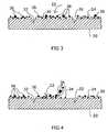
- FIG. 3is a cross-sectional view of the silicon wafer of FIG. 1 taken along line A-A after a laser scribing process has been performed.
- FIG. 4is a cross-sectional view of the silicon wafer of FIG. 1 taken along line A-A after a laser scribing process showing a protective coat being removed.
- FIG. 1shows a top plan pictorial view of a silicon wafer 20 according to an embodiment of the invention.
- the silicon wafer 20includes an array of integrated circuit (IC) dies 22 .
- the IC dies 22include die bumps 24 coupled to an active surface of each IC die.
- the die bumps 24are raised bumps of solder for subsequently connecting a die to a substrate (not shown) in a package.
- the dies 22will be separated from the wafer 20 along lines 26 .
- the wafer 20 and IC dies 22are not shown to scale for illustration purposes.
- a typical silicon wafer 20will have many more IC dies 22 formed on the wafer 20 than is shown in FIG. 1 .
- the number of die bumps 24 per die 22can also vary depending the type of IC die 22 . It is contemplated that embodiments of the invention include dies 22 that utilize types of terminations other than die bumps 24 .
- the wafer 20can include IC dies 22 that are formed with a low dielectric constant (k) interlayer dielectric which can make the wafer 20 brittle thereby making laser scribing useful.
- kdielectric constant
- FIG. 2shows a cross-sectional view of the silicon Wafer 20 taken along line A-A in FIG. 1 .
- a removable, non-soluble protective coat 30is shown applied to the surface of the silicon wafer 20 over the dies 22 and die bumps 24 .
- the protective coat 30may conform to the surface of the wafer 20 and the die bumps 24 .
- the protective coat 30protects the IC die 22 and the die bumps 24 from debris 36 (see FIGS. 3 and 4 ) that is created when the silicon wafer 20 is laser scribed for separating the dies 22 from the wafer 20 . After laser scribing cuts grooves 32 (see FIGS. 3 and 4 ) along lines 26 , the protective coat 30 can then be removed from the die 22 for completion of the packaging process.
- the protective coat 30may be a tape or a film formed from materials such as polyimides, polyvinyl alcohol, methyl cellulose, household transparent tape, PET (polyester), photoresist and soy protein. Certain characteristics of the protective coat 30 can help the protective coat effectively protect the dies 22 and die bumps 24 .
- the protective coat 30may be optically transparent for the visual and fiducial alignment in the laser scribing process and any potentially subsequent saw processes.
- the protective coat 30may also be ablated during the laser scribe process and may be chemically non-interactive with laser energy.
- FIG. 3shows the cross-sectional view of FIG. 2 after a laser scribing process is performed on wafer 20 .
- Grooves 32have been cut into the wafer 20 along lines 26 .
- Debris 36 from the laser scribing processhas been deposited onto the protective coat 30 which keeps the debris 36 from contaminating the IC dies 22 and die bumps 24 .
- the protective coat 30has been ablated by the laser scribing process.
- FIG. 4shows the cross-sectional view of FIGS. 2 and 3 showing the protective coat 30 being peeled from the IC die 22 leaving the IC die 22 and die bumps 24 clean.
- Removing the protective coat 30can include peeling or washing the protective coat 30 off of the dies 22 with water or a chemical solvent. In the case of using solvent to wash the protective coat 30 , the solvent physically washes the protective coat 30 off of the dies 22 and does not dissolve the protective coat. It is contemplated that the protective coat 30 can be removed from the dies 22 either before or after the dies are separated from the silicon wafer 20 .
Landscapes
- Engineering & Computer Science (AREA)
- Physics & Mathematics (AREA)
- Condensed Matter Physics & Semiconductors (AREA)
- General Physics & Mathematics (AREA)
- Manufacturing & Machinery (AREA)
- Computer Hardware Design (AREA)
- Microelectronics & Electronic Packaging (AREA)
- Power Engineering (AREA)
- Laser Beam Processing (AREA)
Abstract
Description
- This disclosure relates to manufacturing integrated circuits from silicon wafers and more specifically to applying a protective coating to the silicon wafer.
- Individual integrated circuit dies (or “dice” as they are sometimes called) are typically manufactured by processing a silicon wafer to create a large array of dies on the wafer. After the dies are formed on the silicon wafer, they must be separated from the wafer.
- Small abrasive saws can be used to cut the dies from the wafer. However, silicon wafers are brittle, especially wafers utilizing a low-dielectric constant (k) interlayer dielectric. Sawing these brittle silicon wafers can result in chipping along the edges of the saw path or kerf. This tending to chip requires larger spacing between dies, which reduces the number of dies that can be produced on a single wafer.
- To help alleviate the need for larger spacing between dies, laser scribing may be used as part of the separating process. A laser creates a groove or other surface discontinuity along a line that may be subsequently sawed (with less chipping due to the smaller thickness being cut) or broken along the line to complete the separation process.
- While laser scribing reduces chipping, the scribing tends to produce debris that accumulates on the surface of the silicon wafer adjacent the groove and across the wafer. This debris can cause problems with flip-chip packaging circuits that have an array of solder balls or die bumps created on the surface of the silicon wafer. These die bumps provide an electrical connection to the integrated circuit. This connection is completed by mounting the die onto a substrate and heating the assembly to create soldered connections between the die and the substrate.
- Debris from the laser scribing that settles on the die bumps or solder balls prevents the solder from properly wetting during the process of attaching the silicon chip to the substrate. Debris can further contaminate other portions of the die. This failure to properly wet and the potential contamination may result in a defective device.
- As a result, when laser scribing is used to separate dies from a silicon wafer, all debris from the laser scribing process should be removed from the silicon wafer prior to the packaging of the dies.
- The description may be best understood by reading the disclosure with reference to the accompanying drawings.
FIG. 1 is a top plan pictorial depiction of a silicon wafer with an array of integrated circuits formed on the wafer according to an embodiment of the invention.FIG. 2 is a cross-sectional view of the silicon wafer ofFIG. 1 taken along line A-A.FIG. 3 is a cross-sectional view of the silicon wafer ofFIG. 1 taken along line A-A after a laser scribing process has been performed.FIG. 4 is a cross-sectional view of the silicon wafer ofFIG. 1 taken along line A-A after a laser scribing process showing a protective coat being removed.FIG. 1 shows a top plan pictorial view of asilicon wafer 20 according to an embodiment of the invention. Thesilicon wafer 20 includes an array of integrated circuit (IC) dies22. In this embodiment, the IC dies22 include diebumps 24 coupled to an active surface of each IC die. Thedie bumps 24 are raised bumps of solder for subsequently connecting a die to a substrate (not shown) in a package. Thedies 22 will be separated from thewafer 20 alonglines 26.- The
wafer 20 andIC dies 22 are not shown to scale for illustration purposes. Atypical silicon wafer 20 will have many more IC dies22 formed on thewafer 20 than is shown inFIG. 1 . The number of diebumps 24 per die22 can also vary depending the type of IC die22. It is contemplated that embodiments of the invention include dies22 that utilize types of terminations other than diebumps 24. Thewafer 20 can includeIC dies 22 that are formed with a low dielectric constant (k) interlayer dielectric which can make thewafer 20 brittle thereby making laser scribing useful. FIG. 2 shows a cross-sectional view of thesilicon Wafer 20 taken along line A-A inFIG. 1 . A removable, non-solubleprotective coat 30 is shown applied to the surface of the silicon wafer20 over thedies 22 and diebumps 24. Theprotective coat 30 may conform to the surface of thewafer 20 and thedie bumps 24.- The
protective coat 30 protects the IC die22 and thedie bumps 24 from debris36 (seeFIGS. 3 and 4 ) that is created when thesilicon wafer 20 is laser scribed for separating thedies 22 from thewafer 20. After laser scribing cuts grooves32 (seeFIGS. 3 and 4 ) alonglines 26, theprotective coat 30 can then be removed from thedie 22 for completion of the packaging process. - The
protective coat 30 may be a tape or a film formed from materials such as polyimides, polyvinyl alcohol, methyl cellulose, household transparent tape, PET (polyester), photoresist and soy protein. Certain characteristics of theprotective coat 30 can help the protective coat effectively protect thedies 22 and diebumps 24. Theprotective coat 30 may be optically transparent for the visual and fiducial alignment in the laser scribing process and any potentially subsequent saw processes. Theprotective coat 30 may also be ablated during the laser scribe process and may be chemically non-interactive with laser energy. FIG. 3 shows the cross-sectional view ofFIG. 2 after a laser scribing process is performed onwafer 20.Grooves 32 have been cut into thewafer 20 alonglines 26.Debris 36 from the laser scribing process has been deposited onto theprotective coat 30 which keeps thedebris 36 from contaminating the IC dies22 and diebumps 24. Here, theprotective coat 30 has been ablated by the laser scribing process.FIG. 4 shows the cross-sectional view ofFIGS. 2 and 3 showing theprotective coat 30 being peeled from the IC die22 leaving the IC die22 and diebumps 24 clean. Removing theprotective coat 30 can include peeling or washing theprotective coat 30 off of thedies 22 with water or a chemical solvent. In the case of using solvent to wash theprotective coat 30, the solvent physically washes theprotective coat 30 off of thedies 22 and does not dissolve the protective coat. It is contemplated that theprotective coat 30 can be removed from thedies 22 either before or after the dies are separated from thesilicon wafer 20.- The preceding embodiments are exemplary. Those of skill in the art will recognize that the concepts taught herein can be tailored to a particular application in many other advantageous ways. In particular, those skilled in the art will recognize that the illustrated embodiments are but one of many alternative implementations that will become apparent upon reading this disclosure.
- Although the specification may refer to “an”, “one”, “another”, or “some” embodiment(s) in several locations, this does not necessarily mean that each such reference is to the same embodiment(s), or that the feature only applies to a single embodiment.
Claims (19)
1. A silicon wafer, comprising:
an array of integrated circuits arranged on a first surface of the silicon wafer; and
a removable non-soluble protective coat on the first surface of the silicon wafer.
2. The silicon wafer ofclaim 1 , comprising die bumps coupled to an active surface of each integrated circuit, where the non-soluble protective coat covers the die bumps.
3. The silicon wafer ofclaim 2 where the removable non-soluble protective coat conforms to the wafer surface and die bumps.
4. The silicon wafer ofclaim 1 where the removable non-soluble protective coat is one of a film and a tape.
5. The silicon wafer ofclaim 1 where the removable non-soluble protective coat is one of a polyimide, polyvinyl alcohol, household transparent tape, and polyester.
6. The silicon wafer ofclaim 1 where the removable non-soluble protective coat is removable by peeling the coat from the first surface of the silicon wafer.
7. The silicon wafer ofclaim 1 where the removable non-soluble protective coat is optically transparent.
8. The silicon wafer ofclaim 1 where the removable non-soluble protective coat is formed of a material that is non-chemically interactive with laser scribing.
9. The silicon wafer ofclaim 1 where the removable non-soluble protective coat is formed of a material that can be ablated by laser energy.
10. The silicon wafer ofclaim 1 where the silicon wafer has a low dielectric constant.
11. A silicon wafer, comprising:
an array of integrated circuits arranged on a first surface of the silicon wafer; and
a non-soluble means for protecting the integrated circuits from debris produced by a laser scribing process.
12. The silicon wafer ofclaim 11 where the integrated circuits include die bumps coupled to an active surface of each integrated circuit; and
the non-soluble means for protecting the integrated circuits protects the die bumps from debris produced by a laser scribing process.
13. The silicon wafer ofclaim 11 where the non-soluble means for protecting the integrated circuits is optically transparent.
14. The silicon wafer ofclaim 11 where the integrated circuits include a low dielectric constant (k) interlayer dielectric.
15. A method for manufacturing an integrated circuit die, comprising:
forming an array of integrated circuit dies on a first surface of a silicon wafer;
applying a non-soluble protective coat to the first surface of the silicon wafer;
laser scribing a groove next to a row of integrated circuit dies;
removing the non-soluble protective coat from the first surface of the silicon wafer; and
separating an integrated circuit die from the silicon wafer.
16. The method ofclaim 15 where forming an array of integrated circuit dies on a first surface of a silicon wafer includes forming die bumps coupled to each of the integrated circuits.
17. The method ofclaim 15 where forming an array of integrated circuit dies includes forming a low dielectric constant (k) interlayer dielectric.
18. The method ofclaim 15 where removing the non-soluble protective coat from the first surface of the silicon wafer includes peeling the non-soluble protective coat from the first surface of the silicon wafer.
19. The method ofclaim 15 where laser scribing a groove includes ablating the non-soluble protective coat.
Priority Applications (1)
| Application Number | Priority Date | Filing Date | Title |
|---|---|---|---|
| US11/159,515US20060289966A1 (en) | 2005-06-22 | 2005-06-22 | Silicon wafer with non-soluble protective coating |
Applications Claiming Priority (1)
| Application Number | Priority Date | Filing Date | Title |
|---|---|---|---|
| US11/159,515US20060289966A1 (en) | 2005-06-22 | 2005-06-22 | Silicon wafer with non-soluble protective coating |
Publications (1)
| Publication Number | Publication Date |
|---|---|
| US20060289966A1true US20060289966A1 (en) | 2006-12-28 |
Family
ID=37566345
Family Applications (1)
| Application Number | Title | Priority Date | Filing Date |
|---|---|---|---|
| US11/159,515AbandonedUS20060289966A1 (en) | 2005-06-22 | 2005-06-22 | Silicon wafer with non-soluble protective coating |
Country Status (1)
| Country | Link |
|---|---|
| US (1) | US20060289966A1 (en) |
Cited By (2)
| Publication number | Priority date | Publication date | Assignee | Title |
|---|---|---|---|---|
| US20150037915A1 (en)* | 2013-07-31 | 2015-02-05 | Wei-Sheng Lei | Method and system for laser focus plane determination in a laser scribing process |
| TWI623060B (en)* | 2009-01-30 | 2018-05-01 | 日東電工股份有限公司 | Dicing tape-integrated wafer back surface protective film,process for producing a semiconductor device using a dicing tape-integrated wafer back surface protective film and flip chip-mounted semiconductor device |
Citations (46)
| Publication number | Priority date | Publication date | Assignee | Title |
|---|---|---|---|---|
| US4704369A (en)* | 1985-04-01 | 1987-11-03 | Energy Conversion Devices, Inc. | Method of severing a semiconductor device |
| US5461099A (en)* | 1993-12-24 | 1995-10-24 | Nissan Chemical Industries, Ltd. | Polyimide varnish |
| US5597767A (en)* | 1995-01-06 | 1997-01-28 | Texas Instruments Incorporated | Separation of wafer into die with wafer-level processing |
| US5641416A (en)* | 1995-10-25 | 1997-06-24 | Micron Display Technology, Inc. | Method for particulate-free energy beam cutting of a wafer of die assemblies |
| US6117347A (en)* | 1996-07-10 | 2000-09-12 | Nec Corporation | Method of separating wafers into individual die |
| US6140707A (en)* | 1998-05-07 | 2000-10-31 | 3M Innovative Properties Co. | Laminated integrated circuit package |
| US6184581B1 (en)* | 1997-11-24 | 2001-02-06 | Delco Electronics Corporation | Solder bump input/output pad for a surface mount circuit device |
| US20010003049A1 (en)* | 1996-07-12 | 2001-06-07 | Norio Fukasawa | Method and mold for manufacturing semiconductor device, semiconductor device, and method for mounting the device |
| US6274389B1 (en)* | 1997-01-17 | 2001-08-14 | Loctite (R&D) Ltd. | Mounting structure and mounting process from semiconductor devices |
| US20020031899A1 (en)* | 1999-06-08 | 2002-03-14 | Ran Manor | Apparatus and method for singulating semiconductor wafers |
| US20030001283A1 (en)* | 2001-06-29 | 2003-01-02 | Takashi Kumamoto | Multi-purpose planarizing/back-grind/pre-underfill arrangements for bumped wafers and dies |
| US20030013233A1 (en)* | 2001-07-13 | 2003-01-16 | Kazutaka Shibata | Semiconductor device and method for manufacturing the same |
| US6582777B1 (en)* | 2000-02-17 | 2003-06-24 | Applied Materials Inc. | Electron beam modification of CVD deposited low dielectric constant materials |
| US6600171B1 (en)* | 2001-04-02 | 2003-07-29 | Micron Technology, Inc. | Semiconductor component and system for fabricating contacts on semiconductor components |
| US20040112880A1 (en)* | 2002-12-13 | 2004-06-17 | Kazuma Sekiya | Laser machining method |
| US20040121514A1 (en)* | 2002-12-23 | 2004-06-24 | Cheol-Joon Yoo | Protective tape removing apparatus and method of assembling semiconductor package using the same |
| US6823585B2 (en)* | 2003-03-28 | 2004-11-30 | International Business Machines Corporation | Method of selective plating on a substrate |
| US20040246692A1 (en)* | 2001-07-12 | 2004-12-09 | Toshiya Satoh | Electronic circuit component |
| US6849524B2 (en)* | 1998-10-23 | 2005-02-01 | Emcore Corporation | Semiconductor wafer protection and cleaning for device separation using laser ablation |
| US20050038276A1 (en)* | 2001-03-17 | 2005-02-17 | Laxman Ravi K. | Low dielectric constant thin films and chemical vapor deposition method of making same |
| US20050070095A1 (en)* | 2003-09-30 | 2005-03-31 | Sujit Sharan | Protective layer during scribing |
| US6897127B2 (en)* | 2002-10-15 | 2005-05-24 | Seiko Epson Corporation | Semiconductor device, method of manufacturing the same, circuit board, and electronic instrument |
| US20050139962A1 (en)* | 2003-12-30 | 2005-06-30 | Dani Ashay A. | Silicon wafer with soluable protective coating |
| US20050148160A1 (en)* | 2002-03-06 | 2005-07-07 | Farnworth Warren M. | Encapsulated semiconductor components and methods of fabrication |
| US6924171B2 (en)* | 2001-02-13 | 2005-08-02 | International Business Machines Corporation | Bilayer wafer-level underfill |
| US20050171301A1 (en)* | 2000-06-09 | 2005-08-04 | Loctite Corporation | Reworkable thermosetting resin compositions |
| US20050202650A1 (en)* | 2004-03-08 | 2005-09-15 | Yoshihisa Imori | Method of dividing a wafer which has a low-k film formed on dicing lines |
| US20050215032A1 (en)* | 2004-03-25 | 2005-09-29 | Seo Joon M | Dicing film having shrinkage release film and method of manufacturing semiconductor package using the same |
| US20050233549A1 (en)* | 2004-04-19 | 2005-10-20 | Hana Microdisplay Technologies, Inc. | Multi-elevation singulation of device laminates in wafer scale and substrate processing |
| US20050263022A1 (en)* | 2004-05-05 | 2005-12-01 | Presstek, Inc. | Lithographic printing with printing members having primer layers |
| US20060011703A1 (en)* | 2002-11-06 | 2006-01-19 | Hitoshi Arita | Solder alloy material layer composition, electroconductive and adhesive composition, flux material layer composition, solder ball transferring sheet, bump and bump forming process, and semiconductore device |
| US20060076046A1 (en)* | 2004-10-08 | 2006-04-13 | Nanocoolers, Inc. | Thermoelectric device structure and apparatus incorporating same |
| US20060079011A1 (en)* | 2000-08-25 | 2006-04-13 | Tandy William D | Methods for marking a bare semiconductor die |
| US20060084297A1 (en)* | 2002-08-27 | 2006-04-20 | Jsr Corporation | Anisotropic conductive sheet, its manufacturing method, and its application |
| US20060097359A1 (en)* | 2004-11-08 | 2006-05-11 | Goodner Michael D | Low-k dielectric layer formed from aluminosilicate precursors |
| US20060165952A1 (en)* | 2003-04-17 | 2006-07-27 | Nanosys, Inc. | Structures, systems and methods for joining articles and materials and uses therefor |
| US7087857B2 (en)* | 2003-08-12 | 2006-08-08 | Disco Corporation | Method of dividing a workpiece in the form of a plate having a layer and a substrate made of different materials |
| US20070178232A1 (en)* | 2001-10-19 | 2007-08-02 | Cabot Corporation | Tape compositions for the deposition of electronic features |
| US7279362B2 (en)* | 2005-03-31 | 2007-10-09 | Intel Corporation | Semiconductor wafer coat layers and methods therefor |
| US7291543B2 (en)* | 2000-12-06 | 2007-11-06 | Micron Technology, Inc. | Thin flip-chip method |
| US20080006900A1 (en)* | 2004-10-21 | 2008-01-10 | Infineon Technologies Ag | Semiconductor Package and Method for Producing the Same |
| US20080118199A1 (en)* | 2003-11-27 | 2008-05-22 | Ibiden Co., Ltd. | Substrate for mounting ic chip, substrate for motherboard, device for optical communication , manufacturing method of substrate for mounting ic chip, and manufacturing method of substrate for motherboard |
| US20080171187A1 (en)* | 2003-06-06 | 2008-07-17 | Teiichi Inada | Adhesive sheet, dicing tape integrated type adhesive sheet, and method of producing semiconductor device |
| US20080251942A1 (en)* | 2004-03-29 | 2008-10-16 | Akira Ohuchi | Semiconductor Device and Manufacturing Method Thereof |
| US20080277799A1 (en)* | 2004-08-27 | 2008-11-13 | Micron Technology, Inc. | Low temperature methods of forming back side redistribution layers in association with through wafer interconnects, semiconductor devices including same, and assemblies |
| US20080296784A1 (en)* | 1999-06-30 | 2008-12-04 | Renesas Technology Corp. | Semiconductor device and a method of manufacturing the same and a mounting structure of a semiconductor device |
- 2005
- 2005-06-22USUS11/159,515patent/US20060289966A1/ennot_activeAbandoned
Patent Citations (49)
| Publication number | Priority date | Publication date | Assignee | Title |
|---|---|---|---|---|
| US4704369A (en)* | 1985-04-01 | 1987-11-03 | Energy Conversion Devices, Inc. | Method of severing a semiconductor device |
| US5461099A (en)* | 1993-12-24 | 1995-10-24 | Nissan Chemical Industries, Ltd. | Polyimide varnish |
| US5597767A (en)* | 1995-01-06 | 1997-01-28 | Texas Instruments Incorporated | Separation of wafer into die with wafer-level processing |
| US5641416A (en)* | 1995-10-25 | 1997-06-24 | Micron Display Technology, Inc. | Method for particulate-free energy beam cutting of a wafer of die assemblies |
| US6117347A (en)* | 1996-07-10 | 2000-09-12 | Nec Corporation | Method of separating wafers into individual die |
| US20010003049A1 (en)* | 1996-07-12 | 2001-06-07 | Norio Fukasawa | Method and mold for manufacturing semiconductor device, semiconductor device, and method for mounting the device |
| US6274389B1 (en)* | 1997-01-17 | 2001-08-14 | Loctite (R&D) Ltd. | Mounting structure and mounting process from semiconductor devices |
| US6184581B1 (en)* | 1997-11-24 | 2001-02-06 | Delco Electronics Corporation | Solder bump input/output pad for a surface mount circuit device |
| US6140707A (en)* | 1998-05-07 | 2000-10-31 | 3M Innovative Properties Co. | Laminated integrated circuit package |
| US6849524B2 (en)* | 1998-10-23 | 2005-02-01 | Emcore Corporation | Semiconductor wafer protection and cleaning for device separation using laser ablation |
| US20020031899A1 (en)* | 1999-06-08 | 2002-03-14 | Ran Manor | Apparatus and method for singulating semiconductor wafers |
| US20080296784A1 (en)* | 1999-06-30 | 2008-12-04 | Renesas Technology Corp. | Semiconductor device and a method of manufacturing the same and a mounting structure of a semiconductor device |
| US6582777B1 (en)* | 2000-02-17 | 2003-06-24 | Applied Materials Inc. | Electron beam modification of CVD deposited low dielectric constant materials |
| US20050171301A1 (en)* | 2000-06-09 | 2005-08-04 | Loctite Corporation | Reworkable thermosetting resin compositions |
| US20060079011A1 (en)* | 2000-08-25 | 2006-04-13 | Tandy William D | Methods for marking a bare semiconductor die |
| US7291543B2 (en)* | 2000-12-06 | 2007-11-06 | Micron Technology, Inc. | Thin flip-chip method |
| US6924171B2 (en)* | 2001-02-13 | 2005-08-02 | International Business Machines Corporation | Bilayer wafer-level underfill |
| US20050038276A1 (en)* | 2001-03-17 | 2005-02-17 | Laxman Ravi K. | Low dielectric constant thin films and chemical vapor deposition method of making same |
| US6600171B1 (en)* | 2001-04-02 | 2003-07-29 | Micron Technology, Inc. | Semiconductor component and system for fabricating contacts on semiconductor components |
| US6794751B2 (en)* | 2001-06-29 | 2004-09-21 | Intel Corporation | Multi-purpose planarizing/back-grind/pre-underfill arrangements for bumped wafers and dies |
| US7071572B2 (en)* | 2001-06-29 | 2006-07-04 | Intel Corporation | Pre-back-grind and underfill layer for bumped wafers and dies |
| US20030001283A1 (en)* | 2001-06-29 | 2003-01-02 | Takashi Kumamoto | Multi-purpose planarizing/back-grind/pre-underfill arrangements for bumped wafers and dies |
| US20040246692A1 (en)* | 2001-07-12 | 2004-12-09 | Toshiya Satoh | Electronic circuit component |
| US20030013233A1 (en)* | 2001-07-13 | 2003-01-16 | Kazutaka Shibata | Semiconductor device and method for manufacturing the same |
| US20070178232A1 (en)* | 2001-10-19 | 2007-08-02 | Cabot Corporation | Tape compositions for the deposition of electronic features |
| US20050148160A1 (en)* | 2002-03-06 | 2005-07-07 | Farnworth Warren M. | Encapsulated semiconductor components and methods of fabrication |
| US20060084297A1 (en)* | 2002-08-27 | 2006-04-20 | Jsr Corporation | Anisotropic conductive sheet, its manufacturing method, and its application |
| US6897127B2 (en)* | 2002-10-15 | 2005-05-24 | Seiko Epson Corporation | Semiconductor device, method of manufacturing the same, circuit board, and electronic instrument |
| US20060011703A1 (en)* | 2002-11-06 | 2006-01-19 | Hitoshi Arita | Solder alloy material layer composition, electroconductive and adhesive composition, flux material layer composition, solder ball transferring sheet, bump and bump forming process, and semiconductore device |
| US20040112880A1 (en)* | 2002-12-13 | 2004-06-17 | Kazuma Sekiya | Laser machining method |
| US20040121514A1 (en)* | 2002-12-23 | 2004-06-24 | Cheol-Joon Yoo | Protective tape removing apparatus and method of assembling semiconductor package using the same |
| US6823585B2 (en)* | 2003-03-28 | 2004-11-30 | International Business Machines Corporation | Method of selective plating on a substrate |
| US20060165952A1 (en)* | 2003-04-17 | 2006-07-27 | Nanosys, Inc. | Structures, systems and methods for joining articles and materials and uses therefor |
| US20080171187A1 (en)* | 2003-06-06 | 2008-07-17 | Teiichi Inada | Adhesive sheet, dicing tape integrated type adhesive sheet, and method of producing semiconductor device |
| US7087857B2 (en)* | 2003-08-12 | 2006-08-08 | Disco Corporation | Method of dividing a workpiece in the form of a plate having a layer and a substrate made of different materials |
| US20050070095A1 (en)* | 2003-09-30 | 2005-03-31 | Sujit Sharan | Protective layer during scribing |
| US20080118199A1 (en)* | 2003-11-27 | 2008-05-22 | Ibiden Co., Ltd. | Substrate for mounting ic chip, substrate for motherboard, device for optical communication , manufacturing method of substrate for mounting ic chip, and manufacturing method of substrate for motherboard |
| US6974726B2 (en)* | 2003-12-30 | 2005-12-13 | Intel Corporation | Silicon wafer with soluble protective coating |
| US20050139962A1 (en)* | 2003-12-30 | 2005-06-30 | Dani Ashay A. | Silicon wafer with soluable protective coating |
| US20050202650A1 (en)* | 2004-03-08 | 2005-09-15 | Yoshihisa Imori | Method of dividing a wafer which has a low-k film formed on dicing lines |
| US20050215032A1 (en)* | 2004-03-25 | 2005-09-29 | Seo Joon M | Dicing film having shrinkage release film and method of manufacturing semiconductor package using the same |
| US20080251942A1 (en)* | 2004-03-29 | 2008-10-16 | Akira Ohuchi | Semiconductor Device and Manufacturing Method Thereof |
| US20050233549A1 (en)* | 2004-04-19 | 2005-10-20 | Hana Microdisplay Technologies, Inc. | Multi-elevation singulation of device laminates in wafer scale and substrate processing |
| US20050263022A1 (en)* | 2004-05-05 | 2005-12-01 | Presstek, Inc. | Lithographic printing with printing members having primer layers |
| US20080277799A1 (en)* | 2004-08-27 | 2008-11-13 | Micron Technology, Inc. | Low temperature methods of forming back side redistribution layers in association with through wafer interconnects, semiconductor devices including same, and assemblies |
| US20060076046A1 (en)* | 2004-10-08 | 2006-04-13 | Nanocoolers, Inc. | Thermoelectric device structure and apparatus incorporating same |
| US20080006900A1 (en)* | 2004-10-21 | 2008-01-10 | Infineon Technologies Ag | Semiconductor Package and Method for Producing the Same |
| US20060097359A1 (en)* | 2004-11-08 | 2006-05-11 | Goodner Michael D | Low-k dielectric layer formed from aluminosilicate precursors |
| US7279362B2 (en)* | 2005-03-31 | 2007-10-09 | Intel Corporation | Semiconductor wafer coat layers and methods therefor |
Cited By (2)
| Publication number | Priority date | Publication date | Assignee | Title |
|---|---|---|---|---|
| TWI623060B (en)* | 2009-01-30 | 2018-05-01 | 日東電工股份有限公司 | Dicing tape-integrated wafer back surface protective film,process for producing a semiconductor device using a dicing tape-integrated wafer back surface protective film and flip chip-mounted semiconductor device |
| US20150037915A1 (en)* | 2013-07-31 | 2015-02-05 | Wei-Sheng Lei | Method and system for laser focus plane determination in a laser scribing process |
Similar Documents
| Publication | Publication Date | Title |
|---|---|---|
| US6582983B1 (en) | Method and wafer for maintaining ultra clean bonding pads on a wafer | |
| US9741619B2 (en) | Methods for singulating semiconductor wafer | |
| US6974726B2 (en) | Silicon wafer with soluble protective coating | |
| US7494900B2 (en) | Back side wafer dicing | |
| KR100337412B1 (en) | An integrated circuit and a semiconductor wafer having a bottom surface protective coating and method of making the same | |
| KR100741864B1 (en) | Method for manufacturing semiconductor device | |
| US7098077B2 (en) | Semiconductor chip singulation method | |
| US20040212047A1 (en) | Edge arrangements for integrated circuit chips | |
| US8361604B2 (en) | Methods and systems for releasably attaching support members to microfeature workpieces | |
| US7265032B2 (en) | Protective layer during scribing | |
| US20110193200A1 (en) | Semiconductor wafer chip scale package test flow and dicing process | |
| US7846776B2 (en) | Methods for releasably attaching sacrificial support members to microfeature workpieces and microfeature devices formed using such methods | |
| KR20180048376A (en) | Method for processing wafer | |
| US11024542B2 (en) | Manufacturing method of device chip | |
| US20060289966A1 (en) | Silicon wafer with non-soluble protective coating | |
| US7071032B2 (en) | Material to improve image sensor yield during wafer sawing | |
| US20240006239A1 (en) | Device wafer processing method | |
| US6759276B1 (en) | Material to improve CMOS image sensor yield during wafer sawing | |
| KR20050020564A (en) | Method and wafer for maintaining ultra clean bonding pads on a wafer | |
| CN115246169A (en) | Wafer cutting equipment and method | |
| KR20010003597A (en) | Semiconductor wafer processing method | |
| KR19980034133A (en) | Wafers with Cut Areas with Long Grooves | |
| KR20100050035A (en) | Back grinding and sawing method for wafer |
Legal Events
| Date | Code | Title | Description |
|---|---|---|---|
| AS | Assignment | Owner name:INTEL CORPORATION (A DELAWARE CORPORATION), CALIFO Free format text:ASSIGNMENT OF ASSIGNORS INTEREST;ASSIGNORS:DANI, ASHAY A.;OSKARSDOTTIR, GUDBJORG H.;MATAYABAS, JAMES, JR.;REEL/FRAME:016727/0658;SIGNING DATES FROM 20050620 TO 20050621 | |
| STCB | Information on status: application discontinuation | Free format text:ABANDONED -- FAILURE TO RESPOND TO AN OFFICE ACTION |