US20060285381A1 - Sensing of resistance variable memory devices - Google Patents
Sensing of resistance variable memory devicesDownload PDFInfo
- Publication number
- US20060285381A1 US20060285381A1US11/473,308US47330806AUS2006285381A1US 20060285381 A1US20060285381 A1US 20060285381A1US 47330806 AUS47330806 AUS 47330806AUS 2006285381 A1US2006285381 A1US 2006285381A1
- Authority
- US
- United States
- Prior art keywords
- cell
- digit
- memory
- circuit
- integrated circuit
- Prior art date
- Legal status (The legal status is an assumption and is not a legal conclusion. Google has not performed a legal analysis and makes no representation as to the accuracy of the status listed.)
- Granted
Links
- 230000015654memoryEffects0.000claimsabstractdescription150
- 230000000295complement effectEffects0.000claimsdescription29
- 230000004044responseEffects0.000claimsdescription4
- 238000000034methodMethods0.000abstractdescription27
- 230000009977dual effectEffects0.000abstractdescription3
- 238000011067equilibrationMethods0.000description51
- 238000002955isolationMethods0.000description13
- 230000002093peripheral effectEffects0.000description6
- 230000004048modificationEffects0.000description3
- 238000012986modificationMethods0.000description3
- 230000003750conditioning effectEffects0.000description2
- 238000004519manufacturing processMethods0.000description2
- 230000037361pathwayEffects0.000description2
- 239000012782phase change materialSubstances0.000description2
- 241000699670Mus sp.Species0.000description1
- 239000005387chalcogenide glassSubstances0.000description1
- 230000008859changeEffects0.000description1
- 230000008030eliminationEffects0.000description1
- 238000003379elimination reactionMethods0.000description1
- 230000006870functionEffects0.000description1
- 230000010354integrationEffects0.000description1
- 239000000463materialSubstances0.000description1
- 229910021645metal ionInorganic materials0.000description1
- 230000008569processEffects0.000description1
Images


Classifications
- G—PHYSICS
- G11—INFORMATION STORAGE
- G11C—STATIC STORES
- G11C13/00—Digital stores characterised by the use of storage elements not covered by groups G11C11/00, G11C23/00, or G11C25/00
- G11C13/0002—Digital stores characterised by the use of storage elements not covered by groups G11C11/00, G11C23/00, or G11C25/00 using resistive RAM [RRAM] elements
- G11C13/0009—RRAM elements whose operation depends upon chemical change
- G11C13/0011—RRAM elements whose operation depends upon chemical change comprising conductive bridging RAM [CBRAM] or programming metallization cells [PMCs]
- G—PHYSICS
- G11—INFORMATION STORAGE
- G11C—STATIC STORES
- G11C13/00—Digital stores characterised by the use of storage elements not covered by groups G11C11/00, G11C23/00, or G11C25/00
- G11C13/0002—Digital stores characterised by the use of storage elements not covered by groups G11C11/00, G11C23/00, or G11C25/00 using resistive RAM [RRAM] elements
- G11C13/0004—Digital stores characterised by the use of storage elements not covered by groups G11C11/00, G11C23/00, or G11C25/00 using resistive RAM [RRAM] elements comprising amorphous/crystalline phase transition cells
- G—PHYSICS
- G11—INFORMATION STORAGE
- G11C—STATIC STORES
- G11C13/00—Digital stores characterised by the use of storage elements not covered by groups G11C11/00, G11C23/00, or G11C25/00
- G11C13/0002—Digital stores characterised by the use of storage elements not covered by groups G11C11/00, G11C23/00, or G11C25/00 using resistive RAM [RRAM] elements
- G11C13/0021—Auxiliary circuits
- G11C13/004—Reading or sensing circuits or methods
- G—PHYSICS
- G11—INFORMATION STORAGE
- G11C—STATIC STORES
- G11C13/00—Digital stores characterised by the use of storage elements not covered by groups G11C11/00, G11C23/00, or G11C25/00
- G11C13/0002—Digital stores characterised by the use of storage elements not covered by groups G11C11/00, G11C23/00, or G11C25/00 using resistive RAM [RRAM] elements
- G11C13/0021—Auxiliary circuits
- G11C13/0069—Writing or programming circuits or methods
- G—PHYSICS
- G11—INFORMATION STORAGE
- G11C—STATIC STORES
- G11C13/00—Digital stores characterised by the use of storage elements not covered by groups G11C11/00, G11C23/00, or G11C25/00
- G11C13/0002—Digital stores characterised by the use of storage elements not covered by groups G11C11/00, G11C23/00, or G11C25/00 using resistive RAM [RRAM] elements
- G11C13/0021—Auxiliary circuits
- G11C13/004—Reading or sensing circuits or methods
- G11C2013/0042—Read using differential sensing, e.g. bit line [BL] and bit line bar [BLB]
- G—PHYSICS
- G11—INFORMATION STORAGE
- G11C—STATIC STORES
- G11C13/00—Digital stores characterised by the use of storage elements not covered by groups G11C11/00, G11C23/00, or G11C25/00
- G11C13/0002—Digital stores characterised by the use of storage elements not covered by groups G11C11/00, G11C23/00, or G11C25/00 using resistive RAM [RRAM] elements
- G11C13/0021—Auxiliary circuits
- G11C13/0069—Writing or programming circuits or methods
- G11C2013/009—Write using potential difference applied between cell electrodes
- G—PHYSICS
- G11—INFORMATION STORAGE
- G11C—STATIC STORES
- G11C2213/00—Indexing scheme relating to G11C13/00 for features not covered by this group
- G11C2213/70—Resistive array aspects
- G11C2213/79—Array wherein the access device being a transistor
Definitions
- the inventionrelates generally to the field of random access memory (RAM) devices and more particularly to the improved sensing of RAM devices formed using a resistance variable material.
- RAMrandom access memory
- Resistance variable memory elementswhich include Programmable Conductive Random Access Memory (PCRAM) elements, have been investigated for suitability as semi-volatile and non-volatile random access memory devices.
- PCRAMProgrammable Conductive Random Access Memory
- the conductivity/resistance of a chalcogenide glass backbonecan be programmed to stable lower conductivity (i.e., higher resistance) and higher conductivity (i.e., lower resistance) states.
- An unprogrammed PCRAM deviceis normally in a lower conductivity, higher resistance state.
- a conditioning operationforms a conducting channel of a metal-chalcogenide in the PCRAM device, which supports a conductive pathway for altering the conductivity/resistivity state of the device.
- a write operationwill program the PCRAM device to a higher conductivity state, in which metal ions accumulate along the conducting channel(s).
- the PCRAM devicemay be read by applying a voltage of a lesser magnitude than required to program it; the current or resistance across the memory device is sensed as higher or lower to define the logic “one” and “zero” states.
- the PCRAMmay be erased by applying a reverse voltage (opposite bias) relative to the write voltage, which disrupts the conductive pathway, but typically leaves the conducting channel intact. In this way, such a device can function as a variable resistance memory having at least two conductivity states, which can define two respective logic states, i.e., at least a bit of data.
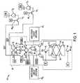
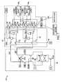
- FIG. 1illustrates a portion of a memory device 10 utilizing resistance variable memory elements as memory cells 12 0 , 12 1 .
- PCRAM elementsare used as the cells 12 0 , 12 1 .
- Each memory cell 12 0 , 12 1has a cell plate connected to a cell plate potential CPIN and is connected to a respective access transistor 14 0 , 14 1 .
- the first access transistor 14 0is connected between the first memory cell 12 0 and a first digit line DIGIT.
- the second access transistor 14 1is connected between the second memory cell 12 1 and a second digit line ⁇ overscore (DIGIT) ⁇ .
- the gates of the access transistors 14 0 , 14 1are connected to word lines WL 0 , WL 1 such that they receive row select signals R 0 , R 1 , respectively.
- the device 10also includes sensing circuitry 30 connected to the digit lines DIGIT, ⁇ overscore (DIGIT) ⁇ .
- the sensing circuitry 30includes an equilibration circuit 32 , two column select transistors 42 , 44 , a reference voltage circuit 50 , two isolating transistors 62 , 64 , a p-sense amplifier driver 78 , a p-sense amplifier circuit 70 , an n-sense amplifier driver 88 and an n-sense amplifier circuit 80 .
- the equilibration (EQ) circuit 32includes three EQ transistors 34 , 36 , 38 .
- the first EQ transistor 34is connected between the two digit lines DIGIT, ⁇ overscore (DIGIT) ⁇ .
- the second EQ transistor 36is connected between the first digit line DIGIT and the third EQ transistor 38 .
- the third EQ transistor 38is connected between the second digit line ⁇ overscore (DIGIT) ⁇ and the second EQ transistor 36 .
- the gate terminals of the three EQ transistors 34 , 36 , 38are connected to an equilibration gating line EQ.
- a bias voltage DVC 2is applied at the connection of the second and third EQ transistors 36 , 38 .
- All three of the EQ transistors 34 , 36 , 38are NMOS transistors.
- the equilibration circuit 32in response to the equilibration gating signal EQ, effectively equalizes the charges held by the digit lines DIGIT, ⁇ overscore (DIGIT) ⁇ after a read/write operation is completed and when the memory array is not active.
- the first column select transistor 42has its source and drain terminals connected between the first digit line DIGIT.
- the second column select transistor 44has its source and drain terminals connected between the second digit line ⁇ overscore (DIGIT) ⁇ .
- the gates of the column select transistors 42 , 44are connected to respective column select lines to receive a column select signal CSEL.
- the column select transistors 42 , 44are activated by the column select signal CSEL when it is desired to connect the remaining circuitry of the sensing circuitry 30 to the memory cells 12 0 , 12 1 (such as for example when it is time to write, erase or read the cells 12 0 , 12 1 ).
- the reference voltage circuit 50includes 4 reference voltage transistors 52 , 54 , 56 , 58 .
- the first reference voltage transistor 52is connected between the first digit line DIGIT and the second reference voltage transistor 54 .
- the second reference voltage transistor 54is connected between the first reference voltage transistor 52 and the second digit line ⁇ overscore (DIGIT) ⁇ .
- DVC 2is applied to the connection between the first and second reference voltage transistors 52 , 54 .
- the third reference voltage transistor 56is connected between the first digit line DIGIT and the fourth reference voltage transistor 58 .
- the fourth reference voltage transistor 58is connected between the third reference voltage transistor 56 and the second digit line ⁇ overscore (DIGIT) ⁇ .
- a reference voltage VREFis applied to the connection between the third and fourth reference voltage transistors 56 , 58 .
- the gate of the first reference voltage transistor 52is connected to the gate of the fourth reference voltage transistor 58 and to a first reference voltage signal REF E.
- the gate of the second reference voltage transistor 54is connected to the gate of the third reference voltage transistor 56 and to a second reference voltage signal REF O.
- the operation of the reference voltage circuit 50is explained below in more detail.
- the first isolating transistor 62is connected between the first digit line DIGIT and a first connection between the p-sense amplifier circuit 70 and the n-sense amplifier circuit 80 .
- the second isolating transistor 64is connected between the second digit line ⁇ overscore (DIGIT) ⁇ and a second connection between the p-sense amplifier circuit 70 and the n-sense amplifier circuit 80 .
- the gate terminals of the first and second isolating transistors 62 , 64are connected to an isolation gating signal SA ISO.
- the illustrated isolating transistors 62 , 64are NMOS transistors.
- the isolating transistors 62 , 64when activated by the isolation gating signal SA ISO, form isolation devices that effectively remove certain portions of the circuit 30 during addressing for a portion of a read and during a write and erase.
- the p-sense amplifier circuit 70includes two PMOS transistors 72 , 74 .
- the n-sense amplifier circuit 80includes two NMOS transistors 82 , 84 .
- the first PMOS transistor 72has its gate terminal connected to the second digit line ⁇ overscore (DIGIT) ⁇ and is connected between the first NMOS transistor 82 and the p-sense amplifier driver 78 .
- the second PMOS transistor 74has its gate terminal connected to the first digit line DIGIT and is connected between the second NMOS transistor 84 and driver 78 .
- the p-sense amplifier driver 78drives the p-sense amplifier 70 when a p-sense amplifier latching signal PL is applied to the gate of the driver 78 .
- the first NMOS transistor 82has its gate terminal connected to the second digit line ⁇ overscore (DIGIT) ⁇ and is connected between the n-sense amplifier driver 88 and the first PMOS transistor 72 .
- the second NMOS transistor 84has its gate terminal connected to the first digit line DIGIT and is connected between driver 88 and the second PMOS transistor 74 .
- the n-sense amplifier driver 88drives the n-sense amplifier 80 when an n-sense amplifier latching signal NL is applied to the gate of the driver 88 .
- Two write/erase circuits 92 0 , 92 1are respectively connected to the digit lines DIGIT, ⁇ overscore (DIGIT) ⁇ via the sensing circuitry 30 .
- the write/erase circuits 92 0 , 92 1apply a first programming voltage VPNS to the digit lines DIGIT, ⁇ overscore (DIGIT) ⁇ when the cells 12 0 or 12 1 are to be written to the high conductivity (i.e., lower resistance) state (as described above) depending on which row R 1 , R 0 is accessed.
- the write/erase circuits 92 0 , 92 1apply a second programming voltage VPPS, typically a reverse voltage (i.e., opposite bias) relative to the first programming voltage VPNS, to the digit lines DIGIT, ⁇ overscore (DIGIT) ⁇ when the cells 12 0 or 12 1 are to be written to the lower conductivity (i.e., higher resistance) state (as described above) depending on which row R 1 or R 0 is accessed.
- the appropriate column select transistors 42 , 44will also need to be activated during the write and erase operations.
- the first reference signal REF Eis generated, which causes the reference voltage circuit 50 to precharge the first digit line DIGIT to DVC 2 (via an activated first column select transistor 42 ).
- the reference voltage circuit 50precharges the second digit line ⁇ overscore (DIGIT) ⁇ to the reference voltage VREF. These precharged values will be applied to the digit lines and to the p-sense amplifier 70 and n-sense amplifier 80 (via activated isolation transistor 64 ).
- the current across the memory cell 12 0is sensed by p-sense amplifier 70 and n-sense amplifier 80 (via activated isolation transistor 62 ) and compared to the reference voltage VREF to determine the state of the memory cell 12 0 once the access transistor 14 0 is turned on.
- the second reference signal REF Ois generated, which causes the reference voltage circuit 50 to apply DVC 2 to the second digit line ⁇ overscore (DIGIT) ⁇ (via an activated second column select transistor 44 and access transistor 14 1 ).
- the reference voltage circuit 50applies the reference voltage VREF to the first digit line, DIGIT. Again, these precharged values will be applied to the digit lines and to the p-sense amplifier 70 and n-sense amplifier 80 (via activated isolation transistor 62 ).
- the current across the memory cell 12 1is sensed by p-sense amplifier 70 and n-sense amplifier 80 (via activated isolation transistor 64 ) and compared to the reference voltage VREF to determine the state of the memory cell 12 1 once the access transistor 141 is turned on.
- PCRAM cellssuch as e.g., cells 12 0 , 12 1
- Changes in the cell plate potential CPIN and the digit line programming voltages VPPS, VPNSallow an addressed cell to be written to or erased.
- the drawbackis that with different potentials for the cell plate and the equilibrated digit lines, non-addressed cells on the same word line may also become partially erased or written.
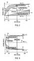
- FIG. 2illustrates a graph of sense time v. digit line voltage for the memory device 10 illustrated in FIG. 1 .
- Line 102represents the digit line voltage for a written cell.
- Line 104represents the digit line voltage for an erased cell. If DVC 2 is 1.0V (line 110 ) and CPIN is 1.2V (line 106 ), VREF is 1.1V (line 108 ).
- sensing differentialat the time the sense amplifiers are latched (e.g., at approximately 150 nS). Most likely, there is approximately a 60 mV differential when the cell is written and about a 40 mV differential when the cell is erased.
- sensing windowfor a resistance variable memory device such as e.g., a PCRAM memory device.
- sensing windowwithout causing the potential across the cell to be greater than approximately 200 mV.
- the inventionincreases the sensing window for a resistance variable memory device such as e.g., a PCRAM memory device.
- the inventionalso increases the sensing window without causing the potential across the cell to be greater than approximately 200 mV.
- the inventionalso provides a technique for writing to resistance variable memory cells while keeping the voltage across non-addressed cells at approximately 0V.
- the inventionalso provides a technique for sensing the state of resistance variable memory cells closer in time to when the cells are accessed (in comparison to typical sensing techniques).
- a resistance variable memory devicesuch as e.g., a PCRAM memory device, with either a 4T (transistor) or 2T memory cell configuration and either a dual cell plate or word line configuration.
- the deviceincludes additional circuitry configured to write or erase addressed cells while keeping the voltage across non-addressed cells at approximately 0V.
- the devicealso includes circuitry that reads the addressed cells in a manner that increases the sensing window without causing the potential across the cell to be greater than approximately 200 mV.
- the devicemay also sense the state of its addressed cells closer in time to when the cells are accessed, in comparison to typical sensing techniques.
- FIG. 1illustrates a portion of a memory device utilizing resistance variable memory elements as memory cells
- FIG. 2illustrates a graph of sense time v. digit line voltage for the memory device illustrated in FIG. 1 ;
- FIG. 3illustrates a graph of sense time v. digit line voltage for a memory device constructed in accordance with the present invention
- FIG. 4illustrates a portion of a memory device, utilizing resistance variable memory elements as memory cells, constructed in accordance with an exemplary embodiment of the invention
- FIG. 5illustrates a portion of the memory device illustrated in FIG. 4 ;
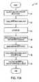
- FIGS. 6A, 6B and 6 Care flowcharts illustrating exemplary methods of operating the device illustrated in FIGS. 4 and 5 ;
- FIG. 7illustrates a portion of a memory device, utilizing resistance variable memory elements as memory cells, constructed in accordance with another exemplary embodiment of the invention
- FIGS. 8A, 8B and 8 Care flowcharts illustrating exemplary methods of operating the device illustrated in FIG. 7 ;
- FIG. 9illustrates a portion of a memory device, utilizing resistance variable memory elements as memory cells, constructed in accordance with yet another exemplary embodiment of the invention.
- FIG. 10illustrates a portion of the memory device illustrated in FIG. 9 ;
- FIGS. 11A, 11B and 11 Care flowcharts illustrating exemplary methods of operating the device illustrated in FIGS. 9 and 10 ;
- FIG. 12shows a processor system incorporating at least one memory device constructed in accordance with an embodiment of the invention.
- FIG. 3depicts a graph of sense time v. digit line voltage for a memory device constructed in accordance with the invention.
- Line 122represents the digit line voltage for a written cell.
- Line 124represents the digit line voltage for an erased cell.
- the graphillustrates two cell plate voltages CPIN 1 (line 122 ) and CPIN 2 (line 124 ). The cell plate voltages CPIN 1 , CPIN 2 are discussed below in more detail.
- DVC 2is 1.0V (line 128 ), CPIN 1 is 1.2V (line 122 ), and CPIN 2 is 0.8V (line 130 ).
- the inventionalso increases the sensing window without causing the potential across the cell to be greater than approximately 200 mv.
- the inventionalso provides a technique for writing to resistance variable memory cells while keeping the voltage across non-addressed cells at approximately 0V.
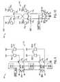
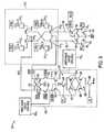
- FIG. 4illustrates a portion of a memory device 210 , utilizing resistance variable memory elements as memory cells 212 0 , 212 1 , 212 2 , 212 3 , constructed in accordance with an exemplary embodiment of the invention.
- PCRAM elementsare used as the cells 212 0 , 212 1 , 212 2 , 212 3 .
- the four memory cells 212 0 , 212 1 , 212 2 , 212 3are connected to the same word line WL via respective access transistors 214 0 , 214 1 , 214 2 , 214 3 .
- the first and third memory cells 212 0 , 212 2are connected to the first cell plate voltage CPIN 1 .
- the second and fourth memory cells 212 1 , 212 3are connected to the second cell plate voltage CPIN 2 .
- the first access transistor 214 0is connected between the first memory cell 212 0 (Cell A) and a right digit line DIGIT R.
- the second access transistor 214 1is connected between the second memory cell 212 1 (Cell B) and a left digit line DIGIT L.
- the third access transistor 214 2is connected between the third memory cell 212 2 ( ⁇ overscore (Cell A) ⁇ ) and a complementary right digit line ⁇ overscore (DIGIT R) ⁇ .
- the fourth access transistor 214 3is connected between the fourth memory cell 212 3 ( ⁇ overscore (Cell B) ⁇ ) and a complementary left digit line ⁇ overscore (DIGIT L) ⁇ .
- the gates of the access transistors 214 0 , 214 1 , 214 2 , 214 3are connected to the same word line WL such that they receive a row select signal R 0 at the same time.
- the memory cells 212 0 , 212 1 , 212 2 , 212 3 and access transistors 214 0 , 214 1 , 214 2 , 214 3make up one large 4T PCRAM cell 212 .
- the device 210also includes write/erase circuitry 290 connected between the digit lines DIGIT R, DIGIT L, ⁇ overscore (DIGIT R) ⁇ , ⁇ overscore (DIGIT L) ⁇ and the first and second digit lines DIGIT, ⁇ overscore (DIGIT) ⁇ .
- the first and second digit lines DIGIT, ⁇ overscore (DIGIT) ⁇are complementary to each other and can be referred to as the digit line DIGIT and complementary digit line ⁇ overscore (DIGIT) ⁇ .
- the write/erase circuitry 290also performs operations during a read operation and is discussed below in more detail.
- the device 210also includes sensing circuitry 230 connected to the first and second digit lines DIGIT, ⁇ overscore (DIGIT) ⁇ .
- the sensing circuitry 230includes an equilibration circuit 232 , two column select transistors 242 , 244 , two isolating transistors 256 , 258 , a p-sense amplifier driver 278 , a p-sense amplifier circuit 270 , an n-sense amplifier driver 288 and an n-sense amplifier circuit 280 .
- the equilibration (EQ) circuit 232includes three EQ transistors 234 , 236 , 238 .
- the first EQ transistor 234is connected between the two digit lines DIGIT, ⁇ overscore (DIGIT) ⁇ .
- the second EQ transistor 236is connected between the first digit line DIGIT and the third EQ transistor 238 .
- the third EQ transistor 238is connected between the second digit line ⁇ overscore (DIGIT) ⁇ and the second EQ transistor 236 .
- the gate terminals of the three EQ transistors 234 , 236 , 238are connected to an equilibration gating line EQ.
- a bias voltage DVC 2is applied at the connection of the second and third EQ transistors 236 , 238 .
- All three of the EQ transistors 234 , 236 , 238are NMOS transistors.
- the equilibration circuit 232in response to the equilibration gating signal EQ, effectively equalizes the charges held by the digit lines DIGIT, ⁇ overscore (DIGIT) ⁇ after a read/write operation is completed and when the memory array is not active.
- the first column select transistor 242has its source and drain terminals connected between the first digit line DIGIT.
- the second column select transistor 244has its source and drain terminals connected between the second digit line ⁇ overscore (DIGIT) ⁇ .
- the gates of the column select transistors 242 , 244are connected to respective column select lines to receive a column select signal CSEL.
- the column select transistors 242 , 244are activated by the column select signal CSEL when it is desired to connect the remaining circuitry of the sensing circuitry 230 to the memory cells 212 0 , 212 1 , 212 2 , 212 3 via circuit 290 and the access transistors 214 0 , 214 1 , 214 2 , 214 3 .
- the first isolating transistor 256is connected between the first digit line DIGIT and a first connection between the p-sense amplifier circuit 270 and the n-sense amplifier circuit 280 .
- the second isolating transistor 258is connected between the second digit line ⁇ overscore (DIGIT) ⁇ and a second connection between the p-sense amplifier circuit 270 and the n-sense amplifier circuit 280 .
- the gate terminals of the first and second isolating transistors 256 , 258are connected to an isolation gating signal SA ISO.
- the illustrated isolating transistors 256 , 258are NMOS transistors. The isolating transistors 256 , 258 , when activated by the isolation gating signal SA ISO, form isolation devices that effectively remove certain portions of the circuit 230 during addressing.
- the p-sense amplifier circuit 270includes two PMOS transistors 272 , 274 .
- the n-sense amplifier circuit 280includes two NMOS transistors 282 , 284 .
- the first PMOS transistor 272has its gate terminal connected to the second digit line ⁇ overscore (DIGIT) ⁇ and is connected between the first NMOS transistor 282 and the p-sense amplifier driver 278 .
- the second PMOS transistor 274has its gate terminal connected to the first digit line DIGIT and is connected between the second NMOS transistor 284 and driver 278 .
- the p-sense amplifier driver 278drives the p-sense amplifier 270 when a p-sense amplifier latching signal PL is applied to the gate of the driver 278 .
- the first NMOS transistor 282has its gate terminal connected to the second digit line ⁇ overscore (DIGIT) ⁇ and is connected between the n-sense amplifier driver 288 and the first PMOS transistor 272 .
- the second NMOS transistor 284has its gate terminal connected to the first digit line DIGIT and is connected between driver 288 and the second PMOS transistor 274 .
- the n-sense amplifier driver 288drives the n-sense amplifier 280 when an n-sense amplifier latching signal NL is applied to the gate of the driver 288 .
- the write/erase circuit 290contains four write/read transistors 300 , 302 , 312 , 314 and four programming column select transistors 304 , 306 , 308 , 310 .
- the first write/read transistor 300is connected between the second write/read transistor 302 and the right digit line DIGIT R.
- the second write/read transistor 302is connected between the first write/read transistor 300 and the left digit line DIGIT L.
- the connection between the first and second write/read transistors 300 , 302is connected to the first digit line DIGIT.
- the gates of the first and second write/read transistors 300 , 302are connected to a write/read control signal ⁇ overscore (WRITE) ⁇ READ.
- the third write/read transistor 312is connected between the fourth write/read transistor 314 and the complementary right digit line ⁇ overscore (DIGIT R) ⁇ .
- the fourth write/read transistor 314is connected between the second write/read transistor 312 and the complementary left digit line ⁇ overscore (DIGIT L) ⁇ .
- the connection between the third and fourth write/read transistors 312 , 314is connected to the complementary digit line ⁇ overscore (DIGIT) ⁇ .
- the gates of the third and fourth write/read transistors 312 , 314are connected to the write/read control signal ⁇ overscore (WRITE) ⁇ READ.
- the first programming column select transistor 304is connected between a first positive programming voltage VPPS 1 and a connection between the left digit line DIGIT L and the complementary right digit line ⁇ overscore (DIGIT R) ⁇ .
- the second programming column select transistor 306is connected between a first negative programming voltage VPNS 1 and a connection between the left digit line DIGIT L and the complementary right digit line ⁇ overscore (DIGIT R) ⁇ .
- the third programming column select transistor 308is connected between a second positive programming voltage VPPS 2 and a connection between the right digit line DIGIT R and the complementary left digit line ⁇ overscore (DIGIT L) ⁇ .
- the fourth programming column select transistor 310is connected between a second negative programming voltage VPNS 2 and a connection between the right digit line DIGIT R and the complementary left digit line ⁇ overscore (DIGIT L) ⁇ .
- the programming column select transistors 304 , 306 , 308 , 310are activated when it is time to write or erase the memory cells 212 0 , 212 1 , 212 2 , 212 3 .
- FIG. 5illustrates a portion of the memory device 210 in a more simplified manner.
- the FIG. 5 illustrationdoes not include the programming column select transistors 304 , 306 , 308 , 310 since it is presumed that they have been activated by the column select signal CSEL.
- the cell plate voltages CPIN 1 , CPIN 2are held at DVC 2 .
- the write/read control signal ⁇ overscore (WRITE) ⁇ READallows the right digit line DIGIT R and complementary left digit line ⁇ overscore (DIGIT L) ⁇ or the left digit line DIGIT and the complementary right digit line ⁇ overscore (DIGIT R) ⁇ to be accessed and programmed by the programming voltages VPPS 1 , VPPS 2 , VPNS 1 , VPNS 2 .
- All other non-accessed memory cells 212 0 , 212 1 , 212 2 , 212 3 associated with the accessed word line WLate not programmed since their top cell plate potential and their respective digit lines are held at DVC 2 . That is, the voltage across the non-addressed cells is approximately 0V.
- the first cell plate voltage CPIN 1is set to DVC 2 +200 mV and the second cell plate voltage is set to DVC 2 ⁇ 200 mV.
- the write/read control signal ⁇ overscore (WRITE) ⁇ READallows the right and left digit lines DIGIT R, DIGIT L to be connected to the sensing circuitry 230
- the accessed memory celleither pulls its digit line up to the first programming voltage CPIN 1 or down to the second programmed voltage CPIN 2 .
- cell 212 0Cell A
- cell 212 3⁇ overscore (Cell B) ⁇
- cell plate potentialse.g., CPIN 1 , CPIN 2
- the access transistors 214 0 , 214 1 , 214 2 , 214 3are activated by applying the row select signal R 0 (step 342 ).
- the write/read control signal ⁇ overscore (WRITE) ⁇ READis toggled low (step 343 ).
- the right digit line DIGIT R and the complementary left digit line ⁇ overscore (DIGIT L) ⁇are pulled to DVC 2 ⁇ 2V to write cell 212 0 (Cell A) and cell 212 3 ( ⁇ overscore (Cell B) ⁇ ) at step 344 .
- the left digit line DIGIT L and the complementary right digit line ⁇ overscore (DIGIT R) ⁇are pulled to DVC 2 +2V to erase cell 212 1 (Cell B) and cell 212 2 ( ⁇ overscore (Cell A) ⁇ ) at step 345 . This places the cell 212 in a high resistance state.
- cell 212 1 (Cell B) and cell 212 2 ( ⁇ overscore (Cell A) ⁇ )are written by writing the second digit line ⁇ overscore (DIGIT) ⁇ to a high state.
- all digit lines DIGIT R, DIGIT L, ⁇ overscore (DIGIT R) ⁇ , ⁇ overscore (DIGIT L) ⁇ and cell plate potentialsare held at DVC 2 (step 351 ).
- the access transistors 214 0 , 214 1 , 214 2 , 214 3are activated by applying the row select signal R 0 (step 352 ).
- the write/read control signal ⁇ overscore (WRITE) ⁇ READis toggled low (step 353 ).
- the left digit line DIGIT L and the complementary right digit line ⁇ overscore (DIGIT R) ⁇are pulled to DVC 2 ⁇ 2V to write cell 212 1 (Cell B) and cell 212 2 ⁇ overscore (Cell A) ⁇ at step 354 .
- the right digit line DIGIT R and the complementary left digit line ⁇ overscore (DIGIT L) ⁇are pulled to DVC 2 +2V to erase cell 212 0 (Cell A) and cell 212 3 ( ⁇ overscore (Cell B) ⁇ ) at step 355 . This places the cell 212 in a low resistance state.
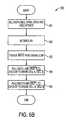
- an exemplary method 360 of operating the memory device 210is now described for a read operation.
- all digit lines DIGIT R, DIGIT L, ⁇ overscore (DIGIT R) ⁇ , ⁇ overscore (DIGIT L) ⁇are held at DVC 2 (step 361 ).
- the first cell plate voltage CPIN 1is set to DVC 2 +200 mV while the second cell plate voltage CPIN 2 is set to DVC 2 ⁇ 200 mV (step 362 ).
- the write/read control signal ⁇ overscore (WRITE) ⁇ READis toggled high (step 363 ) and the column can be accessed and sensed (step 364 ).
- WRITEwrite/read control signal
- FIG. 7illustrates a portion of a memory device 410 , utilizing resistance variable memory elements as memory cells 412 0 , 412 1 , 412 2 , 412 3 in a memory array 411 , constructed in accordance with another exemplary embodiment of the invention.
- PCRAM elementsare used as the cells 412 0 , 412 1 , 412 2 , 412 3 .
- the first two memory cells 412 0 , 412 1are connected to the first digit line DIGIT via access transistor 414 0 and contain different phase change material.
- the third and fourth memory cells 412 2 , 412 3are connected to the second line ⁇ overscore (DIGIT) ⁇ by access transistor 414 1 and contain different phase change material.
- the memory cells 412 0 , 412 1 , 412 2 , 412 3 and access transistors 414 0 , 414 1make up one large 2T PCRAM cell 412 .
- the gates of the access transistors 414 0 , 414 1are connected to the same word line WL such that they receive row select signal R 0 at the same time.
- the digit lines DIGIT, ⁇ overscore (DIGIT) ⁇are connected to sensing circuitry 230 , which is the same sensing circuitry described above with reference to FIG. 4 .
- the device 410also includes write/erase circuitry 490 connected to the cell plates of the memory cells 412 0 , 412 1 , 412 2 , 412 3 .
- the write/erase circuitry 490includes two write/erase circuits 492 0 , 492 1 and eight transistors 500 , 502 , 504 , 506 , 508 , 510 , 512 , 514 .
- the first transistor 500is connected between the second transistor 502 and the first cell plate potential CPIN 1 .
- the second transistor 502is connected between the first transistor 500 and the second write/erase circuit 492 1 .
- the cell plate of the first memory cell 412 0is connected to the connection between the first and second transistors 500 , 502 .
- the third transistor 504is connected between the fourth transistor 506 and the second cell plate potential CPIN 2 .
- the fourth transistor 506is connected between the third transistor 504 and the first write/erase circuit 492 0 .
- the cell plate of the second memory cell 412 1is connected to the connection between the third and fourth transistors 504 , 506 .
- the fifth transistor 508is connected between the sixth transistor 510 and CPIN 1 .
- the sixth transistor 510is connected between the fifth transistor 508 and the second write/erase circuit 492 1 .
- the cell plate of the third memory cell 412 2is connected to the connection between the fifth and sixth transistors 508 , 510 .
- the seventh transistor 512is connected between the eighth transistor 514 and CPIN 2 .
- the eighth transistor 514is connected between the seventh transistor 512 and the first write/erase circuit 492 0 .
- the cell plate of the fourth memory cell 412 3is connected to the connection between the seventh and eighth transistors 504 , 506 .
- the gates of the first, third, fifth and seventh transistors 500 , 504 , 508 , 512are connected to a read signal READ.
- the gates of the second, fourth, sixth and eighth transistors 502 , 506 , 510 , 514are connected to a write signal WRITE.
- the cell plate potentials CPIN 1 , CPIN 2are used to read and the write/erase circuits 492 0 , 492 1 are used to write or erase the memory cells 412 0 , 412 1 , 412 2 , 412 3 .
- a write signal WRITEcauses the cell plates to program the phase change resistance of the cells connected to the digit line DIGIT to one of the two voltages defined by the first write/erase circuit 492 0 (“Write Erase CIRCUIT1”), for this example, DVC 2 +2V.
- the cell on the complementary digit line ⁇ overscore (DIGIT) ⁇is programmed to the opposite voltage defined by the second write/erase circuit 492 1 (“Write Erase CIRCUIT2”), for this example, DVC 2 ⁇ 2V. All other non-accessed digit lines on the same word line are not programmed since their top cell plate and digital lines are at the same potential (i.e., DVC 2 ).
- the first cell plate voltage CPIN 1is set to DVC 2 +200 mV while the second cell plate voltage CPIN 2 is set to DVC 2 ⁇ 200 mV.
- the resistors within the memory cells 412 0 , 412 1 , 412 2 , 412 3are tied to their respective cell plate potentials.
- the programmed resistorse.g., memory cells 412 0 , 412 1 ) pull the digit line DIGIT up to CPIN 1 or down to CPIN 2 depending upon which cell was programmed.
- the cellse.g., memory cells 412 2 , 412 3
- cell 412 0Cell A
- cell 412 3⁇ overscore (Cell B) ⁇
- the digit lines DIGIT, ⁇ overscore (DIGIT) ⁇are held at DVC 2 (step 531 ).
- the access transistors 414 0 , 414 1are activated by applying the row select signal R 0 (step 532 ).
- the top cell plate for (Cell A) and ( ⁇ overscore (Cell B) ⁇ )are set to DVC 2 +2V through Write Erase Circuit 2 once the WRITE signal is given.
- the top cell plate for (Cell B) and ( ⁇ overscore (Cell A) ⁇ )are set to DVC 2 ⁇ 2V through Write Erase Circuit 1 once the WRITE signal is given.
- cell 412 1Cell B
- cell 412 2⁇ overscore (Cell A) ⁇
- the digit lines DIGIT, ⁇ overscore (DIGIT) ⁇are held at DVC 2 (step 541 ).
- the access transistors 414 0 , 414 1are activated by applying the row select signal R 0 (step 542 ).
- the first complementary top cell plates potentialsare set to DCV 2 +2V by the Write Erase CIRCUIT 1 once the WRITE signal is given, to write cell 412 1 (Cell B) and cell 412 2 ( ⁇ overscore (Cell A) ⁇ ) at step 543 .
- the first top cell plate potentialsare set to DCV 2 ⁇ 2V by the Write Erase CIRCUIT 2 once the WRITE signal is given, to erase cell 412 0 (Cell A) and cell 412 3 ( ⁇ overscore (Cell B) ⁇ ) at step 544 . This places the cell 412 in a low resistance state.
- an exemplary method 550 of operating the memory device 410is now described for a read operation.
- the digit lines DIGIT, ⁇ overscore (DIGIT) ⁇are held at DVC 2 (step 551 ).
- the first cell plate potential CPIN 1 and the complementary first cell plate potential CPIN 1are set to DVC 2 +200 mV at step 552 .
- the second cell plate potential CPIN 2 and the second complementary cell plate potential CPIN 2are set to DVC 2 ⁇ 2V at step 553 .
- the cell 412can now be sensed. As noted above, there will be a much larger sensing window as compared to the memory device 10 illustrated in FIGS. 1 and 2 .
- FIG. 9illustrates a portion of a memory device 610 , utilizing resistance variable memory elements as memory cells 612 0 , 612 1 , 612 2 , 612 3 , constructed in accordance with another exemplary embodiment of the invention.
- PCRAM elementsare used as the cells 612 0 , 612 1 , 612 2 , 612 3 .
- the first two memory cells 612 0 , 612 1are connected to the first digit line DIGIT via access transistors 614 0 , 614 1 .
- the other two memory cells 612 2 , 612 3are connected to the complementary digit line ⁇ overscore (DIGIT) ⁇ via access transistors 614 2 , 614 3 .
- DIGITcomplementary digit line ⁇ overscore
- the first and third memory cells 612 0 , 612 2have their cell plates connected to a first cell plate potential CPIN 1 .
- the second and fourth memory cells 612 1 , 612 3have their cell plates connected to a second cell plate potential CPIN 2 .
- the memory cells 612 0 , 612 1 , 612 2 , 612 3 and access transistors 614 0 , 614 1 , 614 2 , 614 3make up one large 4T PCRAM cell 612 with a double word line WL r , WL l .
- the first access transistor 614 0is also connected to the first digit line DIGIT and one terminal of the second access transistor 614 1 .
- the second access transistor 614 1is also connected to the first digit line DIGIT and the first access transistor 614 0 .
- the third access transistor 614 2is connected to the fourth access transistor 614 3 and the complementary digit line ⁇ overscore (DIGIT) ⁇ .
- the gates of the first and fourth access transistors 614 0 , 614 3are connected to receive a right row select signal R 0 r from the right word line WL r via the write/read circuit 700 .
- the gates of the second and third access transistors 614 1 , 614 2are connected to receive a left row select signal R 0 l from the left word line WL l via the write/read circuit 700 .
- the write/read circuit 700includes four write/read transistors 702 , 704 , 706 , 708 .
- the first write/read transistor 702is connected between the second write/read transistor 704 and a line 703 connected to the gates of the second and third access transistors 614 1 , 614 2 .
- the fourth write/read transistor 708is connected between the third write/read transistor 706 and line 703 .
- the second write/read transistor 704is connected between the first write/read transistor 702 and a line 705 connected to the gates of the first and fourth access transistors 614 0 , 614 3 .
- the third write/read transistor 706is connected between the fourth write/read transistor 708 and line 705 .
- the gates of the first and second write/read transistors 702 , 704are connected to receive a row select signal R 0 from a word line WL.
- the gates of the third and fourth write/read transistors 706 , 708are connected to the write/read control signal ⁇ overscore (WRITE) ⁇ READ.
- the digit lines DIGIT, ⁇ overscore (DIGIT) ⁇are connected to sensing circuitry 630 .
- the sensing circuitry 630includes an equilibration circuit 632 , two column select transistors 642 , 644 , two isolating transistors 656 , 658 , a p-sense amplifier driver 678 , a p-sense amplifier circuit 670 , an n-sense amplifier driver 688 and an n-sense amplifier circuit 680 .
- the equilibration (EQ) circuit 632includes three EQ transistors 634 , 636 , 638 .
- the first EQ transistor 634is connected between the two digit lines DIGIT, ⁇ overscore (DIGIT) ⁇ .
- the second EQ transistor 636is connected between the first digit line DIGIT and the third EQ transistor 638 .
- the third EQ transistor 638is connected between the second digit line ⁇ overscore (DIGIT) ⁇ and the second EQ transistor 636 .
- the gate terminals of the three EQ transistors 634 , 636 , 638are connected to an equilibration gating line EQ.
- a bias voltage DVC 2is applied at the connection of the second and third EQ transistors 636 , 638 .
- All three of the EQ transistors 634 , 636 , 638are NMOS transistors.
- the equilibration circuit 632in response to the equilibration gating signal EQ, effectively equalizes the charges held by the digit lines DIGIT, ⁇ overscore (DIGIT) ⁇ after a read/write operation is completed and when the memory array is not active.
- the first column select transistor 642has its source and drain terminals connected between the first digit line DIGIT.
- the second column select transistor 644has its source and drain terminals connected between the second digit line ⁇ overscore (DIGIT) ⁇ .
- the gates of the column select transistors 642 , 644are connected to respective column select lines to receive a column select signal CSEL.
- the column select transistors 642 , 644are activated by the column select signal CSEL when it is desired to connect the remaining circuitry 630 to the memory cells 612 0 , 612 1 , 612 2 , 612 3 .
- the first isolating transistor 656is connected between the first digit line DIGIT and a first connection between the p-sense amplifier circuit 670 and the n-sense amplifier circuit 680 .
- the second isolating transistor 658is connected between the second digit line ⁇ overscore (DIGIT) ⁇ and a second connection between the p-sense amplifier circuit 670 and the n-sense amplifier circuit 680 .
- the gate terminals of the first and second isolating transistors 656 , 658are connected to an isolation gating signal SA ISO.
- the illustrated isolating transistors 656 , 658are NMOS transistors. The isolating transistors 656 , 658 , when activated by the isolation gating signal SA ISO, form isolation devices that effectively remove certain portions of the circuit 630 during addressing.
- the p-sense amplifier circuit 670includes two PMOS transistors 672 , 674 .
- the n-sense amplifier circuit 680includes two NMOS transistors 682 , 684 .
- the first PMOS transistor 672has its gate terminal connected to the second digit line ⁇ overscore (DIGIT) ⁇ and is connected between the first NMOS transistor 682 and the p-sense amplifier driver 678 .
- the second PMOS transistor 674has its gate terminal connected to the first digit line DIGIT and is connected between the second NMOS transistor 684 and driver 678 .
- the p-sense amplifier driver 678drives the p-sense amplifier 670 when a p-sense amplifier latching signal PL is applied to the gate of the driver 678 .
- the first NMOS transistor 682has its gate terminal connected to the second digit line ⁇ overscore (DIGIT) ⁇ and is connected between the n-sense amplifier driver 688 and the first PMOS transistor 672 .
- the second NMOS transistor 684has its gate terminal connected to the first digit line DIGIT and is connected between driver 688 and the second PMOS transistor 674 .
- the n-sense amplifier driver 688drives the n-sense amplifier 680 when an n-sense amplifier latching signal NL is applied to the gate of the driver 688 .
- the device 610also includes write/erase circuitry 692 0 , 692 1 connected to sensing circuitry 630 .
- the first write/erase circuit 692 0is connected to the first digit line DIGIT when the first column select transistor 642 is activated by the column select signal CSEL.
- the second write/erase circuit 692 1is connected to the complementary digit line ⁇ overscore (DIGIT) ⁇ when the second column select transistor 644 is activated by the column select signal CSEL.
- the write/erase circuitry 692 0 , 692 1also performs operations during a read operation and is discussed below in more detail.
- FIG. 10illustrates a portion of the memory device 610 illustrated in FIG. 9 .
- the FIG. 10 illustrationdoes not include the sensing circuitry 630 or the write/erase circuits 692 0 , 692 1 for clarity purposes.
- the cell platesare held at DVC 2 (via CPIN 1 and CPIN 2 ) and the write/read control signal ⁇ overscore (WRITE) ⁇ READ allows the left or right word lines WL l , WL r to access complimentary cells, which are programmed with the VPPS or VPNS potentials that are applied to the digit lines DIGIT, ⁇ overscore (DIGIT) ⁇ . All other non-accessed memory cells 612 0 , 612 1 , 612 2 , 612 3 associated with the accessed word line are not programmed since their top cell plate potential and their respective digit lines are held at DVC 2 . That is, the voltage across the non-addressed cells is approximately 0V.
- the first cell plate potential CPIN 1is set to DVC 2 +200 mV and the second cell plate potential CPIN 2 is set to DVC 2 ⁇ 200 mV.
- the write/read control signal ⁇ overscore (WRITE) ⁇ READis toggled high to turn on the left and right word lines WL l , WL r .
- the programmed cellcan pull its digit line up to CPIN 1 or down to CPIN 2 depending upon which word line WL l , WL r was used to program the cell.
- cell 612 0Cell A
- cell 612 3⁇ overscore (Cell B) ⁇
- the digit lines DIGIT, ⁇ overscore (DIGIT) ⁇ and the cell plate potentials CPIN 1 , CPIN 2are held at DVC 2 (step 731 ).
- the write/read control signal ⁇ overscore (WRITE) ⁇ READis toggled high at step 732 .
- the row select signal R 0is generate (step 733 ).
- the addressed cellsare erased by pulling the digit lines DIGIT, ⁇ overscore (DIGIT) ⁇ to DVC 2 +2V at step 734 .
- the digit lines DIGIT, ⁇ overscore (DIGIT) ⁇are returned to DVC 2 at step 735 .
- the write/read control signal ⁇ overscore (WRITE) ⁇ READis toggled low while the right word line WL r is toggled high and the left word line WL l is toggled low (step 736 ).
- the digit lines DIGIT, ⁇ overscore (DIGIT) ⁇are pulled to DVC 2 ⁇ 2V to write cell 612 0 (Cell A) and cell 612 3 ( ⁇ overscore (Cell B) ⁇ ) at step 737 . This places the cell 612 in a high resistance state.
- cell 612 1Cell B
- cell 612 2⁇ overscore (Cell A) ⁇
- the digit lines DIGIT, ⁇ overscore (DIGIT) ⁇ and the cell plate potentials CPIN 1 , CPIN 2are held at DVC 2 (step 741 ).
- the write/read control signal ⁇ overscore (WRITE) ⁇ READis toggled high at step 742 .
- the row select signal R 0is generate (step 743 ).
- the addressed cellsare erased by pulling the digit lines DIGIT, ⁇ overscore (DIGIT) ⁇ to DVC 2 +2V at step 744 .
- the digit lines DIGIT, ⁇ overscore (DIGIT) ⁇are returned to DVC 2 at step 745 .
- the write/read control signal ⁇ overscore (WRITE) ⁇ READis toggled low while the right word line WL r is toggled low and the left word line WL l is toggled high (step 746 ).
- the digit lines DIGIT, ⁇ overscore (DIGIT) ⁇are pulled to DVC 2 ⁇ 2V to write cell 612 1 (Cell B) and cell 612 2 ( ⁇ overscore (Cell A) ⁇ ) are written to a high state at step 747 . This places the cell 612 in a low resistance state.
- the digit lines DIGIT, ⁇ overscore (DIGIT) ⁇are held at DVC 2 (step 751 ).
- the first cell plate potential CPIN 1is set to DVC 2 +200 mV and the second cell plate potential CPIN 2 is set to DVC 2 ⁇ 2V at step 752 .
- the write/read control signal ⁇ overscore (WRITE) ⁇ READis toggled high while the right and left word lines WL r , WL l are toggled low.
- the columnis then accessed and the sensing of the digit lines DIGIT, ⁇ overscore (DIGIT) ⁇ occurs (step 754 ). As noted above, there will be a much larger sensing window as compared to the memory device 10 illustrated in FIGS. 1 and 2 .
- FIG. 12shows a processor system 900 that may utilize a memory device 100 incorporating one of the embodiments of the invention (i.e., deice 210 , 410 , 610 of FIGS. 4, 7 , 9 ), in accordance with the invention.
- the processing system 900includes one or more processors 901 coupled to a local bus. 904 .
- a memory controller 902 and a primary bus bridge 903are also coupled the local bus 904 .
- the processing system 900may include multiple memory controllers 902 and/or multiple primary bus bridges 903 .
- the memory controller 902 and the primary bus bridge 903may be integrated as a single device 906 .
- the memory controller 902is also coupled to one or more memory buses 907 .
- Each memory bus 907accepts memory components 908 which include at least one memory device 100 of the present invention.
- the memory components 908may be a memory card or a memory module. Examples of memory modules include single inline memory modules (SIMMs) and dual inline memory modules (DIMMs).
- the memory components 908may include one or more additional devices 909 .
- the additional device 909might be a configuration memory, such as a serial presence detect (SPD) memory.
- the memory controller 902may also be coupled to a cache memory 905 .
- the cache memory 905may be the only cache memory in the processing system.
- processors 901may also include cache memories, which may form a cache hierarchy with cache memory 905 .
- the processing system 900includes peripherals or controllers which are bus masters or which support direct memory access (DMA), the memory controller 902 may implement a cache coherency protocol. If the memory controller 902 is coupled to a plurality of memory buses 907 , each memory bus 907 may be operated in parallel, or different address ranges may be mapped to different memory buses 907 .
- DMAdirect memory access
- the primary bus bridge 903is coupled to at least one peripheral bus 910 .
- Various devicessuch as peripherals or additional bus bridges may be coupled to the peripheral bus 910 . These devices may include a storage controller 911 , a miscellaneous I/O device 914 , a secondary bus bridge 915 , a multimedia processor 918 , and a legacy device interface 920 .
- the primary bus bridge 903may also coupled to one or more special purpose high speed ports 922 . In a personal computer, for example, the special purpose port might be the Accelerated Graphics Port (AGP), used to couple a high performance video card to the processing system 900 .
- AGPAccelerated Graphics Port
- the storage controller 911couples one or more storage devices 913 , via a storage bus 912 , to the peripheral bus 910 .
- the storage controller 911may be a SCSI controller and storage devices 913 may be SCSI discs.
- the I/O device 914may be any sort of peripheral.
- the I/O device 914may be a local area network interface, such as an Ethernet card.
- the secondary bus bridge 915may be used to interface additional devices via another bus to the processing system.
- the secondary bus bridge 915may be an universal serial port (USB) controller used to couple USB devices 917 via to the processing system 900 .
- USBuniversal serial port
- the multimedia processor 918may be a sound card, a video capture card, or any other type of media interface, which may also be coupled to one additional devices such as speakers 919 .
- the legacy device interface 920is used to couple legacy devices 921 , for example, older styled keyboards and mice, to the processing system 900 .
- the processing system 900 illustrated in FIG. 12is only an exemplary processing system that may use the memory devices of the invention. While FIG. 12 illustrates a processing architecture especially suitable for a general purpose computer, such as a personal computer or a workstation, it should be recognized that well known modifications can be made to configure the processing system 900 to become more suitable for use in a variety of applications. For example, many electronic devices which require processing may be implemented using a simpler architecture which relies on a CPU 901 coupled to memory components 908 and/or memory devices 100 .
- These electronic devicesmay include, but are not limited to audio/video processors and recorders, gaming consoles, digital television sets, wired or wireless telephones, navigation devices (including system based on the global positioning system (GPS) and/or inertial navigation), and digital cameras and/or recorders.
- the modificationsmay include, for example, elimination of unnecessary components, addition of specialized devices or circuits, and/or integration of a plurality of devices.
- a method of manufacturing a memory deviceincludes the acts of providing an array of memory cells, each cell being connected to first and second digit lines, each cell comprising a plurality of resistance variable memory elements and a plurality of access; and providing sensing circuitry connected to the first and second digit lines, said sensing circuitry sensing the state of an addressed memory cell by changing a cell plate potential of the memory elements within the cell and sensing the difference between the first and second digit lines connected to the addressed cell.
Landscapes
- Chemical & Material Sciences (AREA)
- Crystallography & Structural Chemistry (AREA)
- Semiconductor Memories (AREA)
Abstract
Description
- The invention relates generally to the field of random access memory (RAM) devices and more particularly to the improved sensing of RAM devices formed using a resistance variable material.
- Resistance variable memory elements, which include Programmable Conductive Random Access Memory (PCRAM) elements, have been investigated for suitability as semi-volatile and non-volatile random access memory devices. In a typical PCRAM device, the conductivity/resistance of a chalcogenide glass backbone can be programmed to stable lower conductivity (i.e., higher resistance) and higher conductivity (i.e., lower resistance) states. An unprogrammed PCRAM device is normally in a lower conductivity, higher resistance state.
- A conditioning operation forms a conducting channel of a metal-chalcogenide in the PCRAM device, which supports a conductive pathway for altering the conductivity/resistivity state of the device. After the conditioning operation, a write operation will program the PCRAM device to a higher conductivity state, in which metal ions accumulate along the conducting channel(s). The PCRAM device may be read by applying a voltage of a lesser magnitude than required to program it; the current or resistance across the memory device is sensed as higher or lower to define the logic “one” and “zero” states. The PCRAM may be erased by applying a reverse voltage (opposite bias) relative to the write voltage, which disrupts the conductive pathway, but typically leaves the conducting channel intact. In this way, such a device can function as a variable resistance memory having at least two conductivity states, which can define two respective logic states, i.e., at least a bit of data.
FIG. 1 illustrates a portion of amemory device 10 utilizing resistance variable memory elements as memory cells120,121. For exemplary purposes, PCRAM elements are used as the cells120,121. Each memory cell120,121has a cell plate connected to a cell plate potential CPIN and is connected to a respective access transistor140,141. The first access transistor140is connected between the first memory cell120and a first digit line DIGIT. The second access transistor141is connected between the second memory cell121and a second digit line {overscore (DIGIT)}. The gates of the access transistors140,141are connected to word lines WL0, WL1such that they receive row select signals R0, R1, respectively.- The
device 10 also includessensing circuitry 30 connected to the digit lines DIGIT, {overscore (DIGIT)}. Thesensing circuitry 30 includes anequilibration circuit 32, two columnselect transistors reference voltage circuit 50, twoisolating transistors sense amplifier driver 78, a p-sense amplifier circuit 70, an n-sense amplifier driver 88 and an n-sense amplifier circuit 80. - The equilibration (EQ)
circuit 32 includes threeEQ transistors first EQ transistor 34 is connected between the two digit lines DIGIT, {overscore (DIGIT)}. Thesecond EQ transistor 36 is connected between the first digit line DIGIT and thethird EQ transistor 38. Thethird EQ transistor 38 is connected between the second digit line {overscore (DIGIT)} and thesecond EQ transistor 36. The gate terminals of the threeEQ transistors third EQ transistors EQ transistors equilibration circuit 32, in response to the equilibration gating signal EQ, effectively equalizes the charges held by the digit lines DIGIT, {overscore (DIGIT)} after a read/write operation is completed and when the memory array is not active. - The first column select
transistor 42 has its source and drain terminals connected between the first digit line DIGIT. The second column selecttransistor 44 has its source and drain terminals connected between the second digit line {overscore (DIGIT)}. The gates of the column selecttransistors transistors sensing circuitry 30 to the memory cells120,121(such as for example when it is time to write, erase or read the cells120,121). - The
reference voltage circuit 50 includes 4reference voltage transistors reference voltage transistor 52 is connected between the first digit line DIGIT and the secondreference voltage transistor 54. The secondreference voltage transistor 54 is connected between the firstreference voltage transistor 52 and the second digit line {overscore (DIGIT)}. DVC2 is applied to the connection between the first and secondreference voltage transistors reference voltage transistor 56 is connected between the first digit line DIGIT and the fourthreference voltage transistor 58. The fourthreference voltage transistor 58 is connected between the thirdreference voltage transistor 56 and the second digit line {overscore (DIGIT)}. A reference voltage VREF is applied to the connection between the third and fourthreference voltage transistors - The gate of the first
reference voltage transistor 52 is connected to the gate of the fourthreference voltage transistor 58 and to a first reference voltage signal REF E. The gate of the secondreference voltage transistor 54 is connected to the gate of the thirdreference voltage transistor 56 and to a second reference voltage signal REF O. The operation of thereference voltage circuit 50 is explained below in more detail. - The
first isolating transistor 62 is connected between the first digit line DIGIT and a first connection between the p-sense amplifier circuit 70 and the n-sense amplifier circuit 80. Thesecond isolating transistor 64 is connected between the second digit line {overscore (DIGIT)} and a second connection between the p-sense amplifier circuit 70 and the n-sense amplifier circuit 80. The gate terminals of the first andsecond isolating transistors isolating transistors isolating transistors circuit 30 during addressing for a portion of a read and during a write and erase. - The p-
sense amplifier circuit 70 includes twoPMOS transistors sense amplifier circuit 80 includes twoNMOS transistors first PMOS transistor 72 has its gate terminal connected to the second digit line {overscore (DIGIT)} and is connected between thefirst NMOS transistor 82 and the p-sense amplifier driver 78. Thesecond PMOS transistor 74 has its gate terminal connected to the first digit line DIGIT and is connected between thesecond NMOS transistor 84 anddriver 78. The p-sense amplifier driver 78 drives the p-sense amplifier 70 when a p-sense amplifier latching signal PL is applied to the gate of thedriver 78. - The
first NMOS transistor 82 has its gate terminal connected to the second digit line {overscore (DIGIT)} and is connected between the n-sense amplifier driver 88 and thefirst PMOS transistor 72. Thesecond NMOS transistor 84 has its gate terminal connected to the first digit line DIGIT and is connected betweendriver 88 and thesecond PMOS transistor 74. The n-sense amplifier driver 88 drives the n-sense amplifier 80 when an n-sense amplifier latching signal NL is applied to the gate of thedriver 88. - Two write/erase circuits920,921are respectively connected to the digit lines DIGIT, {overscore (DIGIT)} via the
sensing circuitry 30. The write/erase circuits920,921apply a first programming voltage VPNS to the digit lines DIGIT, {overscore (DIGIT)} when the cells120or121are to be written to the high conductivity (i.e., lower resistance) state (as described above) depending on which row R1, R0 is accessed. The write/erase circuits920,921apply a second programming voltage VPPS, typically a reverse voltage (i.e., opposite bias) relative to the first programming voltage VPNS, to the digit lines DIGIT, {overscore (DIGIT)} when the cells120or121are to be written to the lower conductivity (i.e., higher resistance) state (as described above) depending on which row R1 or R0 is accessed. The appropriate column selecttransistors - To read the first memory cell120, for example, the first reference signal REF E is generated, which causes the
reference voltage circuit 50 to precharge the first digit line DIGIT to DVC2 (via an activated first column select transistor42). In addition, thereference voltage circuit 50 precharges the second digit line {overscore (DIGIT)} to the reference voltage VREF. These precharged values will be applied to the digit lines and to the p-sense amplifier 70 and n-sense amplifier80 (via activated isolation transistor64). The current across the memory cell120is sensed by p-sense amplifier 70 and n-sense amplifier80 (via activated isolation transistor62) and compared to the reference voltage VREF to determine the state of the memory cell120once the access transistor140is turned on. - Similarly, to read the second memory cell121, the second reference signal REF O is generated, which causes the
reference voltage circuit 50 to apply DVC2 to the second digit line {overscore (DIGIT)} (via an activated second column selecttransistor 44 and access transistor141). In addition, thereference voltage circuit 50 applies the reference voltage VREF to the first digit line, DIGIT. Again, these precharged values will be applied to the digit lines and to the p-sense amplifier 70 and n-sense amplifier80 (via activated isolation transistor62). The current across the memory cell121is sensed by p-sense amplifier 70 and n-sense amplifier80 (via activated isolation transistor64) and compared to the reference voltage VREF to determine the state of the memory cell121once theaccess transistor 141 is turned on. - Under the current architecture, PCRAM cells, such as e.g., cells120,121, can only sustain approximately a 200 mV potential across the cell before a partial erase or write occurs. Changes in the cell plate potential CPIN and the digit line programming voltages VPPS, VPNS allow an addressed cell to be written to or erased. The drawback, however, is that with different potentials for the cell plate and the equilibrated digit lines, non-addressed cells on the same word line may also become partially erased or written.
- Typically, a written cell would cause its digit line voltage to approach CPIN, while an erased cell would cause its digit line voltage to approach DVC2. The p-
sense amplifier 70 and n-sense amplifier 80 of thesensing circuitry 30 attempts to differentiate the digit line potential from the reference voltage VREF, which is applied to the complementary digit line.FIG. 2 illustrates a graph of sense time v. digit line voltage for thememory device 10 illustrated inFIG. 1 .Line 102 represents the digit line voltage for a written cell.Line 104 represents the digit line voltage for an erased cell. If DVC2 is 1.0V (line110) and CPIN is 1.2V (line106), VREF is 1.1V (line108). This leaves at most 100 mV of sensing differential at the time the sense amplifiers are latched (e.g., at approximately 150 nS). Most likely, there is approximately a 60 mV differential when the cell is written and about a 40 mV differential when the cell is erased. - There is a need and desire to increase the sensing window for a resistance variable memory device such as e.g., a PCRAM memory device. There is also a need and desire to increase the sensing window without causing the potential across the cell to be greater than approximately 200 mV.
- There is also a need and desire to write to resistance variable memory cells while keeping the voltage across non-addressed cells at approximately 0V. There is also a need and desire to sense the state of resistance variable memory cells closer in time when the cells are accessed, in comparison to typical sensing techniques.
- The invention increases the sensing window for a resistance variable memory device such as e.g., a PCRAM memory device.
- The invention also increases the sensing window without causing the potential across the cell to be greater than approximately 200 mV.
- The invention also provides a technique for writing to resistance variable memory cells while keeping the voltage across non-addressed cells at approximately 0V.
- The invention also provides a technique for sensing the state of resistance variable memory cells closer in time to when the cells are accessed (in comparison to typical sensing techniques).
- The above and other features and advantages are achieved in various exemplary embodiments of the invention by providing a resistance variable memory device such as e.g., a PCRAM memory device, with either a 4T (transistor) or 2T memory cell configuration and either a dual cell plate or word line configuration. The device includes additional circuitry configured to write or erase addressed cells while keeping the voltage across non-addressed cells at approximately 0V. The device also includes circuitry that reads the addressed cells in a manner that increases the sensing window without causing the potential across the cell to be greater than approximately 200 mV. The device may also sense the state of its addressed cells closer in time to when the cells are accessed, in comparison to typical sensing techniques.
- The foregoing and other advantages and features of the invention will become more apparent from the detailed description of exemplary embodiments provided below with reference to the accompanying drawings in which:
FIG. 1 illustrates a portion of a memory device utilizing resistance variable memory elements as memory cells;FIG. 2 illustrates a graph of sense time v. digit line voltage for the memory device illustrated inFIG. 1 ;FIG. 3 illustrates a graph of sense time v. digit line voltage for a memory device constructed in accordance with the present invention;FIG. 4 illustrates a portion of a memory device, utilizing resistance variable memory elements as memory cells, constructed in accordance with an exemplary embodiment of the invention;FIG. 5 illustrates a portion of the memory device illustrated inFIG. 4 ;FIGS. 6A, 6B and6C are flowcharts illustrating exemplary methods of operating the device illustrated inFIGS. 4 and 5 ;FIG. 7 illustrates a portion of a memory device, utilizing resistance variable memory elements as memory cells, constructed in accordance with another exemplary embodiment of the invention;FIGS. 8A, 8B and8C are flowcharts illustrating exemplary methods of operating the device illustrated inFIG. 7 ;FIG. 9 illustrates a portion of a memory device, utilizing resistance variable memory elements as memory cells, constructed in accordance with yet another exemplary embodiment of the invention;FIG. 10 illustrates a portion of the memory device illustrated inFIG. 9 ;FIGS. 11A, 11B and11C are flowcharts illustrating exemplary methods of operating the device illustrated inFIGS. 9 and 10 ; andFIG. 12 shows a processor system incorporating at least one memory device constructed in accordance with an embodiment of the invention.- The exemplary embodiments of the invention increase the sensing window for a resistance variable memory device such as e.g., a PCRAM memory device. This is illustrated in
FIG. 3 , which depicts a graph of sense time v. digit line voltage for a memory device constructed in accordance with the invention.Line 122 represents the digit line voltage for a written cell.Line 124 represents the digit line voltage for an erased cell. The graph illustrates two cell plate voltages CPIN1 (line122) and CPIN2 (line124). The cell plate voltages CPIN1, CPIN2 are discussed below in more detail. DVC2 is 1.0V (line128), CPIN1 is 1.2V (line122), and CPIN2 is 0.8V (line130). This provides approximately 240 mV of sensing differential at a much earlier time (t=50 nS) in comparison to thememory device 10 illustrated inFIGS. 1 and 2 . Thus, if the sense amplifiers were latched at this time (i.e., t=50 nS), there will be a larger sensing differential and the latching would occur 100 nS sooner than thememory device 10 ofFIGS. 1 and 2 . Moreover, there is an approximately 360 mV sensing differential at time t=150 nS, which is approximately 260 mV larger than thememory device 10 ofFIGS. 1 and 2 . - As is discussed below in more detail, the invention also increases the sensing window without causing the potential across the cell to be greater than approximately 200 mv. The invention also provides a technique for writing to resistance variable memory cells while keeping the voltage across non-addressed cells at approximately 0V.
FIG. 4 illustrates a portion of amemory device 210, utilizing resistance variable memory elements asmemory cells cells memory cells third memory cells fourth memory cells - The first access transistor2140is connected between the first memory cell2120(Cell A) and a right digit line DIGIT R. The second access transistor2141is connected between the second memory cell2121(Cell B) and a left digit line DIGIT L. The third access transistor2142is connected between the third memory cell2122({overscore (Cell A)}) and a complementary right digit line {overscore (DIGIT R)}. The fourth access transistor2143is connected between the fourth memory cell2123({overscore (Cell B)}) and a complementary left digit line {overscore (DIGIT L)}. The gates of the access transistors2140,2141,2142,2143are connected to the same word line WL such that they receive a row select signal R0 at the same time. The
memory cells 4T PCRAM cell 212. - The
device 210 also includes write/erasecircuitry 290 connected between the digit lines DIGIT R, DIGIT L, {overscore (DIGIT R)}, {overscore (DIGIT L)} and the first and second digit lines DIGIT, {overscore (DIGIT)}. The first and second digit lines DIGIT, {overscore (DIGIT)} are complementary to each other and can be referred to as the digit line DIGIT and complementary digit line {overscore (DIGIT)}. The write/erasecircuitry 290 also performs operations during a read operation and is discussed below in more detail. - The
device 210 also includessensing circuitry 230 connected to the first and second digit lines DIGIT, {overscore (DIGIT)}. Thesensing circuitry 230 includes anequilibration circuit 232, two columnselect transistors transistors sense amplifier driver 278, a p-sense amplifier circuit 270, an n-sense amplifier driver 288 and an n-sense amplifier circuit 280. - The equilibration (EQ)
circuit 232 includes threeEQ transistors first EQ transistor 234 is connected between the two digit lines DIGIT, {overscore (DIGIT)}. Thesecond EQ transistor 236 is connected between the first digit line DIGIT and the third EQ transistor238. The third EQ transistor238 is connected between the second digit line {overscore (DIGIT)} and thesecond EQ transistor 236. The gate terminals of the threeEQ transistors third EQ transistors 236,238. All three of theEQ transistors equilibration circuit 232, in response to the equilibration gating signal EQ, effectively equalizes the charges held by the digit lines DIGIT, {overscore (DIGIT)} after a read/write operation is completed and when the memory array is not active. - The first column
select transistor 242 has its source and drain terminals connected between the first digit line DIGIT. The second columnselect transistor 244 has its source and drain terminals connected between the second digit line {overscore (DIGIT)}. The gates of the columnselect transistors select transistors sensing circuitry 230 to thememory cells circuit 290 and the access transistors2140,2141,2142,2143. - The first isolating
transistor 256 is connected between the first digit line DIGIT and a first connection between the p-sense amplifier circuit 270 and the n-sense amplifier circuit 280. The second isolatingtransistor 258 is connected between the second digit line {overscore (DIGIT)} and a second connection between the p-sense amplifier circuit 270 and the n-sense amplifier circuit 280. The gate terminals of the first and second isolatingtransistors transistors transistors circuit 230 during addressing. - The p-
sense amplifier circuit 270 includes twoPMOS transistors sense amplifier circuit 280 includes twoNMOS transistors first PMOS transistor 272 has its gate terminal connected to the second digit line {overscore (DIGIT)} and is connected between thefirst NMOS transistor 282 and the p-sense amplifier driver 278. Thesecond PMOS transistor 274 has its gate terminal connected to the first digit line DIGIT and is connected between thesecond NMOS transistor 284 anddriver 278. The p-sense amplifier driver 278 drives the p-sense amplifier 270 when a p-sense amplifier latching signal PL is applied to the gate of thedriver 278. - The
first NMOS transistor 282 has its gate terminal connected to the second digit line {overscore (DIGIT)} and is connected between the n-sense amplifier driver 288 and thefirst PMOS transistor 272. Thesecond NMOS transistor 284 has its gate terminal connected to the first digit line DIGIT and is connected betweendriver 288 and thesecond PMOS transistor 274. The n-sense amplifier driver 288 drives the n-sense amplifier 280 when an n-sense amplifier latching signal NL is applied to the gate of thedriver 288. - The write/erase
circuit 290 contains four write/readtransistors select transistors read transistor 300 is connected between the second write/read transistor 302 and the right digit line DIGIT R. The second write/read transistor 302 is connected between the first write/read transistor 300 and the left digit line DIGIT L. The connection between the first and second write/readtransistors transistors - The third write/
read transistor 312 is connected between the fourth write/read transistor 314 and the complementary right digit line {overscore (DIGIT R)}. The fourth write/read transistor 314 is connected between the second write/read transistor 312 and the complementary left digit line {overscore (DIGIT L)}. The connection between the third and fourth write/readtransistors transistors - The first programming column select transistor304 is connected between a first positive programming voltage VPPS1 and a connection between the left digit line DIGIT L and the complementary right digit line {overscore (DIGIT R)}. The second programming column
select transistor 306 is connected between a first negative programming voltage VPNS1 and a connection between the left digit line DIGIT L and the complementary right digit line {overscore (DIGIT R)}. The third programming columnselect transistor 308 is connected between a second positive programming voltage VPPS2 and a connection between the right digit line DIGIT R and the complementary left digit line {overscore (DIGIT L)}. The fourth programming columnselect transistor 310 is connected between a second negative programming voltage VPNS2 and a connection between the right digit line DIGIT R and the complementary left digit line {overscore (DIGIT L)}. The programming columnselect transistors memory cells - The operation of the
memory device 210 is now described with reference toFIGS. 5 and 6 A-6C.FIG. 5 illustrates a portion of thememory device 210 in a more simplified manner. TheFIG. 5 illustration does not include the programming columnselect transistors - Generally, to write or erase the
memory cells non-accessed memory cells - Generally, during a read operation, the first cell plate voltage CPIN1 is set to DVC2+200 mV and the second cell plate voltage is set to DVC2−200 mV. When the write/read control signal {overscore (WRITE)}READ allows the right and left digit lines DIGIT R, DIGIT L to be connected to the
sensing circuitry 230, the accessed memory cell either pulls its digit line up to the first programming voltage CPIN1 or down to the second programmed voltage CPIN2. The complementary digit line is programmed to be pulled to the opposite cell plate potential. As shown inFIG. 3 , this creates an approximately 380 mV sensing differential at time t=50 nS. - Referring to
FIGS. 5 and 6 A, anexemplary method 340 of operating thememory device 210 is now described. In the illustratedmethod 340, cell2120(Cell A) and cell2123({overscore (Cell B)}) are written by writing the first digit line DIGIT to a high state. Initially, all digit lines DIGIT R, DIGIT L, {overscore (DIGIT R)}, {overscore (DIGIT L)} and cell plate potentials (e.g., CPIN1, CPIN2) are held at DVC2 (step341). The access transistors2140,2141,2142,2143are activated by applying the row select signal R0 (step342). The write/read control signal {overscore (WRITE)}READ is toggled low (step343). The right digit line DIGIT R and the complementary left digit line {overscore (DIGIT L)} are pulled to DVC2−2V to write cell2120(Cell A) and cell2123({overscore (Cell B)}) atstep 344. The left digit line DIGIT L and the complementary right digit line {overscore (DIGIT R)} are pulled to DVC2+2V to erase cell2121(Cell B) and cell2122({overscore (Cell A)}) atstep 345. This places thecell 212 in a high resistance state. - Referring to
FIGS. 5 and 6 B, anotherexemplary method 350 of operating thememory device 210 is now described. In the illustratedmethod 350, cell2121(Cell B) and cell2122({overscore (Cell A)}) are written by writing the second digit line {overscore (DIGIT)} to a high state. Initially, all digit lines DIGIT R, DIGIT L, {overscore (DIGIT R)}, {overscore (DIGIT L)} and cell plate potentials (e.g., CPIN1, CPIN2) are held at DVC2 (step351). The access transistors2140,2141,2142,2143are activated by applying the row select signal R0 (step352). The write/read control signal {overscore (WRITE)}READ is toggled low (step353). The left digit line DIGIT L and the complementary right digit line {overscore (DIGIT R)} are pulled to DVC2−2V to write cell2121(Cell B) and cell2122{overscore (Cell A)} atstep 354. The right digit line DIGIT R and the complementary left digit line {overscore (DIGIT L)} are pulled to DVC2+2V to erase cell2120(Cell A) and cell2123({overscore (Cell B)}) atstep 355. This places thecell 212 in a low resistance state. - Referring to
FIGS. 5 and 6 C, anexemplary method 360 of operating thememory device 210 is now described for a read operation. Initially, all digit lines DIGIT R, DIGIT L, {overscore (DIGIT R)}, {overscore (DIGIT L)} are held at DVC2 (step361). Next, the first cell plate voltage CPIN1 is set to DVC2+200 mV while the second cell plate voltage CPIN2 is set to DVC2−200 mV (step362). The write/read control signal {overscore (WRITE)}READ is toggled high (step363) and the column can be accessed and sensed (step364). As noted above, there will be a much larger sensing window as compared to thememory device 10 illustrated inFIGS. 1 and 2 . FIG. 7 illustrates a portion of amemory device 410, utilizing resistance variable memory elements asmemory cells memory array 411, constructed in accordance with another exemplary embodiment of the invention. For exemplary purposes, PCRAM elements are used as thecells memory cells fourth memory cells memory cells 2T PCRAM cell 412.- The gates of the access transistors4140,4141, are connected to the same word line WL such that they receive row select signal R0 at the same time. The digit lines DIGIT, {overscore (DIGIT)} are connected to sensing
circuitry 230, which is the same sensing circuitry described above with reference toFIG. 4 . - The
device 410 also includes write/erasecircuitry 490 connected to the cell plates of thememory cells circuitry 490 includes two write/erase circuits4920,4921and eighttransistors - The
first transistor 500 is connected between thesecond transistor 502 and the first cell plate potential CPIN1. Thesecond transistor 502 is connected between thefirst transistor 500 and the second write/erase circuit4921. The cell plate of thefirst memory cell 4120is connected to the connection between the first andsecond transistors third transistor 504 is connected between thefourth transistor 506 and the second cell plate potential CPIN2. Thefourth transistor 506 is connected between thethird transistor 504 and the first write/erase circuit4920. The cell plate of thesecond memory cell 4121is connected to the connection between the third andfourth transistors - The
fifth transistor 508 is connected between thesixth transistor 510 and CPIN1. Thesixth transistor 510 is connected between thefifth transistor 508 and the second write/erase circuit4921. The cell plate of thethird memory cell 4122is connected to the connection between the fifth andsixth transistors seventh transistor 512 is connected between theeighth transistor 514 and CPIN2. Theeighth transistor 514 is connected between theseventh transistor 512 and the first write/erase circuit4920. The cell plate of thefourth memory cell 4123is connected to the connection between the seventh andeighth transistors seventh transistors eighth transistors - Generally, the cell plate potentials CPIN1, CPIN2 are used to read and the write/erase circuits4920,4921are used to write or erase the
memory cells - Generally, during a read operation, the first cell plate voltage CPIN1 is set to DVC2+200 mV while the second cell plate voltage CPIN2 is set to DVC2−200 mV. When the read signal READ is toggled high, the resistors within the
memory cells memory cells 4120,4121) pull the digit line DIGIT up to CPIN1 or down to CPIN2 depending upon which cell was programmed. The cells (e.g.,memory cells 4122,4123) on the complementary digit line {overscore (DIGIT)} pull the complementary digit line {overscore (DIGIT)} in the opposite direction. This opens up the sensing window to approximately 380 mV at time t=150 nS as shown inFIG. 3 . - Referring to
FIGS. 7 and 8 A, anexemplary method 530 of operating thememory device 410 is now described. In the illustratedmethod 530, cell4120(Cell A) and cell4123({overscore (Cell B)}) are written to a high state. Initially, the digit lines DIGIT, {overscore (DIGIT)} are held at DVC2 (step531). The access transistors4140,4141are activated by applying the row select signal R0 (step532). The top cell plate for (Cell A) and ({overscore (Cell B)}) are set to DVC2+2V through Write EraseCircuit 2 once the WRITE signal is given. This will write cell4120(Cell A) and cell4123({overscore (Cell B)}) atstep 533. The top cell plate for (Cell B) and ({overscore (Cell A)}) are set to DVC2−2V through Write EraseCircuit 1 once the WRITE signal is given. This will erase cell4121(Cell B) and cell4122({overscore (Cell A)}) atstep 534. This places thecell 412 in a high resistance state. - Referring to
FIGS. 7 and 8 B, anotherexemplary method 540 of operating thememory device 410 is now described. In the illustratedmethod 540, cell4121(Cell B) and cell4122({overscore (Cell A)}) are written to a high state. Initially, the digit lines DIGIT, {overscore (DIGIT)} are held at DVC2 (step541). The access transistors4140,4141are activated by applying the row select signal R0 (step542). The first complementary top cell plates potentials are set to DCV2+2V by the Write EraseCIRCUIT 1 once the WRITE signal is given, to write cell4121(Cell B) and cell4122({overscore (Cell A)}) atstep 543. The first top cell plate potentials are set to DCV2−2V by the Write EraseCIRCUIT 2 once the WRITE signal is given, to erase cell4120(Cell A) and cell4123({overscore (Cell B)}) atstep 544. This places thecell 412 in a low resistance state. - Referring to
FIGS. 7 and 8 C, anexemplary method 550 of operating thememory device 410 is now described for a read operation. Initially, the digit lines DIGIT, {overscore (DIGIT)} are held at DVC2 (step551). The first cell plate potential CPIN1 and the complementary first cell plate potential CPIN1 are set to DVC2+200 mV atstep 552. The second cell plate potential CPIN2 and the second complementary cell plate potential CPIN2 are set to DVC2−2V atstep 553. Thecell 412 can now be sensed. As noted above, there will be a much larger sensing window as compared to thememory device 10 illustrated inFIGS. 1 and 2 . FIG. 9 illustrates a portion of amemory device 610, utilizing resistance variable memory elements asmemory cells cells memory cells memory cells third memory cells fourth memory cells - The
memory cells 4T PCRAM cell 612 with a double word line WLr, WLl. The first access transistor6140is also connected to the first digit line DIGIT and one terminal of the second access transistor6141. The second access transistor6141is also connected to the first digit line DIGIT and the first access transistor6140. The third access transistor6142is connected to the fourth access transistor6143and the complementary digit line {overscore (DIGIT)}. The gates of the first and fourth access transistors6140,6143are connected to receive a right row select signal R0rfrom the right word line WLrvia the write/read circuit 700. The gates of the second and third access transistors6141,6142are connected to receive a left row select signal R0lfrom the left word line WLlvia the write/read circuit 700. - The write/
read circuit 700 includes four write/readtransistors read transistor 702 is connected between the second write/read transistor 704 and aline 703 connected to the gates of the second and third access transistors6141,6142. The fourth write/read transistor 708 is connected between the third write/read transistor 706 andline 703. The second write/read transistor 704 is connected between the first write/read transistor 702 and aline 705 connected to the gates of the first and fourth access transistors6140,6143. The third write/read transistor 706 is connected between the fourth write/read transistor 708 andline 705. The gates of the first and second write/readtransistors transistors - The digit lines DIGIT, {overscore (DIGIT)} are connected to sensing
circuitry 630. Thesensing circuitry 630 includes anequilibration circuit 632, two columnselect transistors transistors sense amplifier driver 678, a p-sense amplifier circuit 670, an n-sense amplifier driver 688 and an n-sense amplifier circuit 680. - The equilibration (EQ)
circuit 632 includes threeEQ transistors first EQ transistor 634 is connected between the two digit lines DIGIT, {overscore (DIGIT)}. Thesecond EQ transistor 636 is connected between the first digit line DIGIT and thethird EQ transistor 638. Thethird EQ transistor 638 is connected between the second digit line {overscore (DIGIT)} and thesecond EQ transistor 636. The gate terminals of the threeEQ transistors third EQ transistors EQ transistors equilibration circuit 632, in response to the equilibration gating signal EQ, effectively equalizes the charges held by the digit lines DIGIT, {overscore (DIGIT)} after a read/write operation is completed and when the memory array is not active. - The first column
select transistor 642 has its source and drain terminals connected between the first digit line DIGIT. The second columnselect transistor 644 has its source and drain terminals connected between the second digit line {overscore (DIGIT)}. The gates of the columnselect transistors select transistors circuitry 630 to thememory cells - The first isolating
transistor 656 is connected between the first digit line DIGIT and a first connection between the p-sense amplifier circuit 670 and the n-sense amplifier circuit 680. The second isolatingtransistor 658 is connected between the second digit line {overscore (DIGIT)} and a second connection between the p-sense amplifier circuit 670 and the n-sense amplifier circuit 680. The gate terminals of the first and second isolatingtransistors transistors transistors circuit 630 during addressing. - The p-
sense amplifier circuit 670 includes twoPMOS transistors sense amplifier circuit 680 includes twoNMOS transistors first PMOS transistor 672 has its gate terminal connected to the second digit line {overscore (DIGIT)} and is connected between thefirst NMOS transistor 682 and the p-sense amplifier driver 678. Thesecond PMOS transistor 674 has its gate terminal connected to the first digit line DIGIT and is connected between thesecond NMOS transistor 684 anddriver 678. The p-sense amplifier driver 678 drives the p-sense amplifier 670 when a p-sense amplifier latching signal PL is applied to the gate of thedriver 678. - The
first NMOS transistor 682 has its gate terminal connected to the second digit line {overscore (DIGIT)} and is connected between the n-sense amplifier driver 688 and thefirst PMOS transistor 672. Thesecond NMOS transistor 684 has its gate terminal connected to the first digit line DIGIT and is connected betweendriver 688 and thesecond PMOS transistor 674. The n-sense amplifier driver 688 drives the n-sense amplifier 680 when an n-sense amplifier latching signal NL is applied to the gate of thedriver 688. - The
device 610 also includes write/erase circuitry6920,6921connected to sensingcircuitry 630. The first write/erase circuit6920is connected to the first digit line DIGIT when the first columnselect transistor 642 is activated by the column select signal CSEL. The second write/erase circuit6921is connected to the complementary digit line {overscore (DIGIT)} when the second columnselect transistor 644 is activated by the column select signal CSEL. The write/erase circuitry6920,6921also performs operations during a read operation and is discussed below in more detail. FIG. 10 illustrates a portion of thememory device 610 illustrated inFIG. 9 . TheFIG. 10 illustration does not include thesensing circuitry 630 or the write/erase circuits6920,6921for clarity purposes.- Generally, to write or erase the
cells non-accessed memory cells - During a read operation, the first cell plate potential CPIN1 is set to DVC2+200 mV and the second cell plate potential CPIN2 is set to DVC2−200 mV. The write/read control signal {overscore (WRITE)}READ is toggled high to turn on the left and right word lines WLl, WLr. The programmed cell can pull its digit line up to CPIN1 or down to CPIN2 depending upon which word line WLl, WLrwas used to program the cell. The complimentary digit line is pulled to the opposite cell plate potential. This opens up the sensing window to approximately 380 mV at time t=150 nS as shown in
FIG. 3 . - Referring to
FIGS. 10 and 11 A, anexemplary method 730 of operating thememory device 610 is now described. In the illustratedmethod 730, cell6120(Cell A) and cell6123({overscore (Cell B)}) are written to a high state. Initially, the digit lines DIGIT, {overscore (DIGIT)} and the cell plate potentials CPIN1, CPIN2 are held at DVC2 (step731). The write/read control signal {overscore (WRITE)}READ is toggled high atstep 732. The row select signal R0 is generate (step733). The addressed cells are erased by pulling the digit lines DIGIT, {overscore (DIGIT)} to DVC2+2V atstep 734. The digit lines DIGIT, {overscore (DIGIT)} are returned to DVC2 atstep 735. The write/read control signal {overscore (WRITE)}READ is toggled low while the right word line WLris toggled high and the left word line WLlis toggled low (step736). The digit lines DIGIT, {overscore (DIGIT)} are pulled to DVC2−2V to write cell6120(Cell A) and cell6123({overscore (Cell B)}) atstep 737. This places thecell 612 in a high resistance state. - Referring to
FIGS. 10 and 11 B, anexemplary method 740 of operating thememory device 610 is now described. In the illustratedmethod 740, cell6121(Cell B) and cell6122({overscore (Cell A)}) are written to a high state. Initially, the digit lines DIGIT, {overscore (DIGIT)} and the cell plate potentials CPIN1, CPIN2 are held at DVC2 (step741). The write/read control signal {overscore (WRITE)}READ is toggled high atstep 742. The row select signal R0 is generate (step743). The addressed cells are erased by pulling the digit lines DIGIT, {overscore (DIGIT)} to DVC2+2V atstep 744. The digit lines DIGIT, {overscore (DIGIT)} are returned to DVC2 atstep 745. The write/read control signal {overscore (WRITE)}READ is toggled low while the right word line WLris toggled low and the left word line WLlis toggled high (step746). The digit lines DIGIT, {overscore (DIGIT)} are pulled to DVC2−2V to write cell6121(Cell B) and cell6122({overscore (Cell A)}) are written to a high state atstep 747. This places thecell 612 in a low resistance state. - Referring to
FIGS. 10 and 11 C, anexemplary method 750 of operating thememory device 610 is now described for a read operation. Initially, the digit lines DIGIT, {overscore (DIGIT)} are held at DVC2 (step751). The first cell plate potential CPIN1 is set to DVC2+200 mV and the second cell plate potential CPIN2 is set to DVC2−2V atstep 752. Atstep 753, the write/read control signal {overscore (WRITE)}READ is toggled high while the right and left word lines WLr, WLlare toggled low. The column is then accessed and the sensing of the digit lines DIGIT, {overscore (DIGIT)} occurs (step754). As noted above, there will be a much larger sensing window as compared to thememory device 10 illustrated inFIGS. 1 and 2 . FIG. 12 shows aprocessor system 900 that may utilize amemory device 100 incorporating one of the embodiments of the invention (i.e.,deice FIGS. 4, 7 ,9), in accordance with the invention. Theprocessing system 900 includes one ormore processors 901 coupled to a local bus.904. Amemory controller 902 and aprimary bus bridge 903 are also coupled thelocal bus 904. Theprocessing system 900 may includemultiple memory controllers 902 and/or multiple primary bus bridges903. Thememory controller 902 and theprimary bus bridge 903 may be integrated as asingle device 906.- The
memory controller 902 is also coupled to one ormore memory buses 907. Eachmemory bus 907 acceptsmemory components 908 which include at least onememory device 100 of the present invention. Thememory components 908 may be a memory card or a memory module. Examples of memory modules include single inline memory modules (SIMMs) and dual inline memory modules (DIMMs). Thememory components 908 may include one or moreadditional devices 909. For example, in a SIMM or DIMM, theadditional device 909 might be a configuration memory, such as a serial presence detect (SPD) memory. Thememory controller 902 may also be coupled to acache memory 905. Thecache memory 905 may be the only cache memory in the processing system. Alternatively, other devices, for example,processors 901 may also include cache memories, which may form a cache hierarchy withcache memory 905. If theprocessing system 900 includes peripherals or controllers which are bus masters or which support direct memory access (DMA), thememory controller 902 may implement a cache coherency protocol. If thememory controller 902 is coupled to a plurality ofmemory buses 907, eachmemory bus 907 may be operated in parallel, or different address ranges may be mapped todifferent memory buses 907. - The
primary bus bridge 903 is coupled to at least one peripheral bus910. Various devices, such as peripherals or additional bus bridges may be coupled to the peripheral bus910. These devices may include astorage controller 911, a miscellaneous I/O device 914, asecondary bus bridge 915, amultimedia processor 918, and alegacy device interface 920. Theprimary bus bridge 903 may also coupled to one or more special purposehigh speed ports 922. In a personal computer, for example, the special purpose port might be the Accelerated Graphics Port (AGP), used to couple a high performance video card to theprocessing system 900. - The
storage controller 911 couples one ormore storage devices 913, via astorage bus 912, to the peripheral bus910. For example, thestorage controller 911 may be a SCSI controller andstorage devices 913 may be SCSI discs. The I/O device 914 may be any sort of peripheral. For example, the I/O device 914 may be a local area network interface, such as an Ethernet card. Thesecondary bus bridge 915 may be used to interface additional devices via another bus to the processing system. For example, thesecondary bus bridge 915 may be an universal serial port (USB) controller used to couple USB devices917 via to theprocessing system 900. Themultimedia processor 918 may be a sound card, a video capture card, or any other type of media interface, which may also be coupled to one additional devices such asspeakers 919. Thelegacy device interface 920 is used to couplelegacy devices 921, for example, older styled keyboards and mice, to theprocessing system 900. - The
processing system 900 illustrated inFIG. 12 is only an exemplary processing system that may use the memory devices of the invention. WhileFIG. 12 illustrates a processing architecture especially suitable for a general purpose computer, such as a personal computer or a workstation, it should be recognized that well known modifications can be made to configure theprocessing system 900 to become more suitable for use in a variety of applications. For example, many electronic devices which require processing may be implemented using a simpler architecture which relies on aCPU 901 coupled tomemory components 908 and/ormemory devices 100. These electronic devices may include, but are not limited to audio/video processors and recorders, gaming consoles, digital television sets, wired or wireless telephones, navigation devices (including system based on the global positioning system (GPS) and/or inertial navigation), and digital cameras and/or recorders. The modifications may include, for example, elimination of unnecessary components, addition of specialized devices or circuits, and/or integration of a plurality of devices. - It should be appreciated that other embodiments of the invention include a method of manufacturing the
devices - The processes and devices described above illustrate preferred methods and typical devices of many that could be used and produced. The above description and drawings illustrate embodiments, which achieve the objects, features, and advantages of the present invention. However, it is not intended that the present invention be strictly limited to the above-described and illustrated embodiments. Any modification, though presently unforeseeable, of the present invention that comes within the spirit and scope of the following claims should be considered part of the present invention.
Claims (27)
Priority Applications (1)
| Application Number | Priority Date | Filing Date | Title |
|---|---|---|---|
| US11/473,308US7190608B2 (en) | 2004-09-01 | 2006-06-23 | Sensing of resistance variable memory devices |
Applications Claiming Priority (2)
| Application Number | Priority Date | Filing Date | Title |
|---|---|---|---|
| US10/931,129US7151688B2 (en) | 2004-09-01 | 2004-09-01 | Sensing of resistance variable memory devices |
| US11/473,308US7190608B2 (en) | 2004-09-01 | 2006-06-23 | Sensing of resistance variable memory devices |
Related Parent Applications (1)
| Application Number | Title | Priority Date | Filing Date |
|---|---|---|---|
| US10/931,129ContinuationUS7151688B2 (en) | 2004-09-01 | 2004-09-01 | Sensing of resistance variable memory devices |
Publications (2)
| Publication Number | Publication Date |
|---|---|
| US20060285381A1true US20060285381A1 (en) | 2006-12-21 |
| US7190608B2 US7190608B2 (en) | 2007-03-13 |
Family
ID=35942841
Family Applications (2)
| Application Number | Title | Priority Date | Filing Date |
|---|---|---|---|
| US10/931,129Expired - LifetimeUS7151688B2 (en) | 2004-09-01 | 2004-09-01 | Sensing of resistance variable memory devices |
| US11/473,308Expired - LifetimeUS7190608B2 (en) | 2004-09-01 | 2006-06-23 | Sensing of resistance variable memory devices |
Family Applications Before (1)
| Application Number | Title | Priority Date | Filing Date |
|---|---|---|---|
| US10/931,129Expired - LifetimeUS7151688B2 (en) | 2004-09-01 | 2004-09-01 | Sensing of resistance variable memory devices |
Country Status (1)
| Country | Link |
|---|---|
| US (2) | US7151688B2 (en) |
Families Citing this family (8)
| Publication number | Priority date | Publication date | Assignee | Title |
|---|---|---|---|---|
| DE102004047638B4 (en)* | 2004-09-30 | 2011-12-01 | Qimonda Ag | Non-volatile memory cell |
| US7269079B2 (en) | 2005-05-16 | 2007-09-11 | Micron Technology, Inc. | Power circuits for reducing a number of power supply voltage taps required for sensing a resistive memory |
| US7813167B2 (en) | 2008-03-21 | 2010-10-12 | Micron Technology, Inc. | Memory cell |
| US7881100B2 (en)* | 2008-04-08 | 2011-02-01 | Micron Technology, Inc. | State machine sensing of memory cells |
| US7825479B2 (en)* | 2008-08-06 | 2010-11-02 | International Business Machines Corporation | Electrical antifuse having a multi-thickness dielectric layer |
| US8208330B2 (en)* | 2009-07-24 | 2012-06-26 | Macronix International Co., Ltd. | Sense amplifier with shielding circuit |
| US9361975B2 (en) | 2013-03-11 | 2016-06-07 | Adesto Technologies Corporation | Sensing data in resistive switching memory devices |
| US9761312B1 (en)* | 2016-03-16 | 2017-09-12 | Micron Technology, Inc. | FeRAM-DRAM hybrid memory |
Citations (93)
| Publication number | Priority date | Publication date | Assignee | Title |
|---|---|---|---|---|
| US3961314A (en)* | 1974-03-05 | 1976-06-01 | Energy Conversion Devices, Inc. | Structure and method for producing an image |
| US3966317A (en)* | 1974-04-08 | 1976-06-29 | Energy Conversion Devices, Inc. | Dry process production of archival microform records from hard copy |
| US4267261A (en)* | 1971-07-15 | 1981-05-12 | Energy Conversion Devices, Inc. | Method for full format imaging |
| US4269935A (en)* | 1979-07-13 | 1981-05-26 | Ionomet Company, Inc. | Process of doping silver image in chalcogenide layer |
| US4312938A (en)* | 1979-07-06 | 1982-01-26 | Drexler Technology Corporation | Method for making a broadband reflective laser recording and data storage medium with absorptive underlayer |
| US4316946A (en)* | 1979-12-03 | 1982-02-23 | Ionomet Company, Inc. | Surface sensitized chalcogenide product and process for making and using the same |
| US4320191A (en)* | 1978-11-07 | 1982-03-16 | Nippon Telegraph & Telephone Public Corporation | Pattern-forming process |
| US4499557A (en)* | 1980-10-28 | 1985-02-12 | Energy Conversion Devices, Inc. | Programmable cell for use in programmable electronic arrays |
| US4637895A (en)* | 1985-04-01 | 1987-01-20 | Energy Conversion Devices, Inc. | Gas mixtures for the vapor deposition of semiconductor material |
| US4646266A (en)* | 1984-09-28 | 1987-02-24 | Energy Conversion Devices, Inc. | Programmable semiconductor structures and methods for using the same |
| US4664939A (en)* | 1985-04-01 | 1987-05-12 | Energy Conversion Devices, Inc. | Vertical semiconductor processor |
| US4668968A (en)* | 1984-05-14 | 1987-05-26 | Energy Conversion Devices, Inc. | Integrated circuit compatible thin film field effect transistor and method of making same |
| US4670763A (en)* | 1984-05-14 | 1987-06-02 | Energy Conversion Devices, Inc. | Thin film field effect transistor |
| US4671618A (en)* | 1986-05-22 | 1987-06-09 | Wu Bao Gang | Liquid crystalline-plastic material having submillisecond switch times and extended memory |
| US4673957A (en)* | 1984-05-14 | 1987-06-16 | Energy Conversion Devices, Inc. | Integrated circuit compatible thin film field effect transistor and method of making same |
| US4728406A (en)* | 1986-08-18 | 1988-03-01 | Energy Conversion Devices, Inc. | Method for plasma - coating a semiconductor body |
| US4737379A (en)* | 1982-09-24 | 1988-04-12 | Energy Conversion Devices, Inc. | Plasma deposited coatings, and low temperature plasma method of making same |
| US4795657A (en)* | 1984-04-13 | 1989-01-03 | Energy Conversion Devices, Inc. | Method of fabricating a programmable array |
| US4809044A (en)* | 1986-08-22 | 1989-02-28 | Energy Conversion Devices, Inc. | Thin film overvoltage protection devices |
| US4818717A (en)* | 1986-06-27 | 1989-04-04 | Energy Conversion Devices, Inc. | Method for making electronic matrix arrays |
| US4843443A (en)* | 1984-05-14 | 1989-06-27 | Energy Conversion Devices, Inc. | Thin film field effect transistor and method of making same |
| US4891330A (en)* | 1987-07-27 | 1990-01-02 | Energy Conversion Devices, Inc. | Method of fabricating n-type and p-type microcrystalline semiconductor alloy material including band gap widening elements |
| US5177567A (en)* | 1991-07-19 | 1993-01-05 | Energy Conversion Devices, Inc. | Thin-film structure for chalcogenide electrical switching devices and process therefor |
| US5219788A (en)* | 1991-02-25 | 1993-06-15 | Ibm Corporation | Bilayer metallization cap for photolithography |
| US5296716A (en)* | 1991-01-18 | 1994-03-22 | Energy Conversion Devices, Inc. | Electrically erasable, directly overwritable, multibit single cell memory elements and arrays fabricated therefrom |
| US5315131A (en)* | 1990-11-22 | 1994-05-24 | Matsushita Electric Industrial Co., Ltd. | Electrically reprogrammable nonvolatile memory device |
| US5314772A (en)* | 1990-10-09 | 1994-05-24 | Arizona Board Of Regents | High resolution, multi-layer resist for microlithography and method therefor |
| US5406509A (en)* | 1991-01-18 | 1995-04-11 | Energy Conversion Devices, Inc. | Electrically erasable, directly overwritable, multibit single cell memory elements and arrays fabricated therefrom |
| US5414271A (en)* | 1991-01-18 | 1995-05-09 | Energy Conversion Devices, Inc. | Electrically erasable memory elements having improved set resistance stability |
| US5500532A (en)* | 1994-08-18 | 1996-03-19 | Arizona Board Of Regents | Personal electronic dosimeter |
| US5512773A (en)* | 1993-12-23 | 1996-04-30 | U.S. Philips Corporation | Switching element with memory provided with Schottky tunnelling barrier |
| US5512328A (en)* | 1992-08-07 | 1996-04-30 | Hitachi, Ltd. | Method for forming a pattern and forming a thin film used in pattern formation |
| US5591501A (en)* | 1995-12-20 | 1997-01-07 | Energy Conversion Devices, Inc. | Optical recording medium having a plurality of discrete phase change data recording points |
| US5596522A (en)* | 1991-01-18 | 1997-01-21 | Energy Conversion Devices, Inc. | Homogeneous compositions of microcrystalline semiconductor material, semiconductor devices and directly overwritable memory elements fabricated therefrom, and arrays fabricated from the memory elements |
| US5714768A (en)* | 1995-10-24 | 1998-02-03 | Energy Conversion Devices, Inc. | Second-layer phase change memory array on top of a logic device |
| US5726083A (en)* | 1994-11-29 | 1998-03-10 | Nec Corporation | Process of fabricating dynamic random access memory device having storage capacitor low in contact resistance and small in leakage current through tantalum oxide film |
| US5751012A (en)* | 1995-06-07 | 1998-05-12 | Micron Technology, Inc. | Polysilicon pillar diode for use in a non-volatile memory cell |
| US5761115A (en)* | 1996-05-30 | 1998-06-02 | Axon Technologies Corporation | Programmable metallization cell structure and method of making same |
| US5869843A (en)* | 1995-06-07 | 1999-02-09 | Micron Technology, Inc. | Memory array having a multi-state element and method for forming such array or cells thereof |
| US5912839A (en)* | 1998-06-23 | 1999-06-15 | Energy Conversion Devices, Inc. | Universal memory element and method of programming same |
| US6011757A (en)* | 1998-01-27 | 2000-01-04 | Ovshinsky; Stanford R. | Optical recording media having increased erasability |
| US6031287A (en)* | 1997-06-18 | 2000-02-29 | Micron Technology, Inc. | Contact structure and memory element incorporating the same |
| US6177338B1 (en)* | 1999-02-08 | 2001-01-23 | Taiwan Semiconductor Manufacturing Company | Two step barrier process |
| US6236059B1 (en)* | 1996-08-22 | 2001-05-22 | Micron Technology, Inc. | Memory cell incorporating a chalcogenide element and method of making same |
| US20020000666A1 (en)* | 1998-08-31 | 2002-01-03 | Michael N. Kozicki | Self-repairing interconnections for electrical circuits |
| US6339544B1 (en)* | 2000-09-29 | 2002-01-15 | Intel Corporation | Method to enhance performance of thermal resistor device |
| US6348365B1 (en)* | 2001-03-02 | 2002-02-19 | Micron Technology, Inc. | PCRAM cell manufacturing |
| US6350679B1 (en)* | 1999-08-03 | 2002-02-26 | Micron Technology, Inc. | Methods of providing an interlevel dielectric layer intermediate different elevation conductive metal layers in the fabrication of integrated circuitry |
| US6376284B1 (en)* | 1996-02-23 | 2002-04-23 | Micron Technology, Inc. | Method of fabricating a memory device |
| US6391688B1 (en)* | 1995-06-07 | 2002-05-21 | Micron Technology, Inc. | Method for fabricating an array of ultra-small pores for chalcogenide memory cells |
| US20030001229A1 (en)* | 2001-03-01 | 2003-01-02 | Moore John T. | Chalcogenide comprising device |
| US6507061B1 (en)* | 2001-08-31 | 2003-01-14 | Intel Corporation | Multiple layer phase-change memory |
| US6511862B2 (en)* | 2001-06-30 | 2003-01-28 | Ovonyx, Inc. | Modified contact for programmable devices |
| US6511867B2 (en)* | 2001-06-30 | 2003-01-28 | Ovonyx, Inc. | Utilizing atomic layer deposition for programmable device |
| US6512241B1 (en)* | 2001-12-31 | 2003-01-28 | Intel Corporation | Phase change material memory device |
| US6514805B2 (en)* | 2001-06-30 | 2003-02-04 | Intel Corporation | Trench sidewall profile for device isolation |
| US20030027416A1 (en)* | 2001-08-01 | 2003-02-06 | Moore John T. | Method of forming integrated circuitry, method of forming memory circuitry, and method of forming random access memory circuitry |
| US20030032254A1 (en)* | 2000-12-08 | 2003-02-13 | Gilton Terry L. | Resistance variable device, analog memory device, and programmable memory cell |
| US20030035315A1 (en)* | 2001-04-06 | 2003-02-20 | Kozicki Michael N. | Microelectronic device, structure, and system, including a memory structure having a variable programmable property and method of forming the same |
| US20030035314A1 (en)* | 1998-12-04 | 2003-02-20 | Kozicki Michael N. | Programmable microelectronic devices and methods of forming and programming same |
| US20030038301A1 (en)* | 2001-08-27 | 2003-02-27 | John Moore | Apparatus and method for dual cell common electrode PCRAM memory device |
| US20030045054A1 (en)* | 2001-08-29 | 2003-03-06 | Campbell Kristy A. | Method of forming non-volatile resistance variable devices, method of forming a programmable memory cell of memory circuitry, and a non-volatile resistance variable device |
| US20030043631A1 (en)* | 2001-08-30 | 2003-03-06 | Gilton Terry L. | Method of retaining memory state in a programmable conductor RAM |
| US20030045049A1 (en)* | 2001-08-29 | 2003-03-06 | Campbell Kristy A. | Method of forming chalcogenide comprising devices |
| US6531373B2 (en)* | 2000-12-27 | 2003-03-11 | Ovonyx, Inc. | Method of forming a phase-change memory cell using silicon on insulator low electrode in charcogenide elements |
| US20030047772A1 (en)* | 2001-03-15 | 2003-03-13 | Jiutao Li | Agglomeration elimination for metal sputter deposition of chalcogenides |
| US20030048744A1 (en)* | 2001-09-01 | 2003-03-13 | Ovshinsky Stanford R. | Increased data storage in optical data storage and retrieval systems using blue lasers and/or plasmon lenses |
| US20030047765A1 (en)* | 2001-08-30 | 2003-03-13 | Campbell Kristy A. | Stoichiometry for chalcogenide glasses useful for memory devices and method of formation |
| US20030049912A1 (en)* | 2001-08-29 | 2003-03-13 | Campbell Kristy A. | Method of forming chalcogenide comprsing devices and method of forming a programmable memory cell of memory circuitry |
| US20030048519A1 (en)* | 2000-02-11 | 2003-03-13 | Kozicki Michael N. | Microelectronic photonic structure and device and method of forming the same |
| US6534781B2 (en)* | 2000-12-26 | 2003-03-18 | Ovonyx, Inc. | Phase-change memory bipolar array utilizing a single shallow trench isolation for creating an individual active area region for two memory array elements and one bipolar base contact |
| US6545907B1 (en)* | 2001-10-30 | 2003-04-08 | Ovonyx, Inc. | Technique and apparatus for performing write operations to a phase change material memory device |
| US6545287B2 (en)* | 2001-09-07 | 2003-04-08 | Intel Corporation | Using selective deposition to form phase-change memory cells |
| US20030068861A1 (en)* | 2001-08-30 | 2003-04-10 | Jiutao Li | Integrated circuit device and fabrication using metal-doped chalcogenide materials |
| US6555860B2 (en)* | 2000-09-29 | 2003-04-29 | Intel Corporation | Compositionally modified resistive electrode |
| US6563164B2 (en)* | 2000-09-29 | 2003-05-13 | Ovonyx, Inc. | Compositionally modified resistive electrode |
| US6566700B2 (en)* | 2001-10-11 | 2003-05-20 | Ovonyx, Inc. | Carbon-containing interfacial layer for phase-change memory |
| US6567293B1 (en)* | 2000-09-29 | 2003-05-20 | Ovonyx, Inc. | Single level metal memory cell using chalcogenide cladding |
| US20030095426A1 (en)* | 2001-11-20 | 2003-05-22 | Glen Hush | Complementary bit PCRAM sense amplifier and method of operation |
| US20030096497A1 (en)* | 2001-11-19 | 2003-05-22 | Micron Technology, Inc. | Electrode structure for use in an integrated circuit |
| US6569705B2 (en)* | 2000-12-21 | 2003-05-27 | Intel Corporation | Metal structure for a phase-change memory device |
| US6570784B2 (en)* | 2001-06-29 | 2003-05-27 | Ovonyx, Inc. | Programming a phase-change material memory |
| US6673648B2 (en)* | 2001-11-08 | 2004-01-06 | Intel Corporation | Isolating phase change material memory cells |
| US6673700B2 (en)* | 2001-06-30 | 2004-01-06 | Ovonyx, Inc. | Reduced area intersection between electrode and programming element |
| US6687427B2 (en)* | 2000-12-29 | 2004-02-03 | Intel Corporation | Optic switch |
| US6690026B2 (en)* | 2001-09-28 | 2004-02-10 | Intel Corporation | Method of fabricating a three-dimensional array of active media |
| US6696355B2 (en)* | 2000-12-14 | 2004-02-24 | Ovonyx, Inc. | Method to selectively increase the top resistance of the lower programming electrode in a phase-change memory |
| US20040035401A1 (en)* | 2002-08-26 | 2004-02-26 | Subramanian Ramachandran | Hydrogen powered scooter |
| US6707712B2 (en)* | 2001-08-02 | 2004-03-16 | Intel Corporation | Method for reading a structural phase-change memory |
| US6714954B2 (en)* | 2002-05-10 | 2004-03-30 | Energy Conversion Devices, Inc. | Methods of factoring and modular arithmetic |
| US20040071042A1 (en)* | 2002-01-04 | 2004-04-15 | John Moore | PCRAM rewrite prevention |
| US6731528B2 (en)* | 2002-05-03 | 2004-05-04 | Micron Technology, Inc. | Dual write cycle programmable conductor memory system and method of operation |
| US6888745B2 (en)* | 2002-12-05 | 2005-05-03 | Sharp Kabushiki Kaisha | Nonvolatile memory device |
Family Cites Families (94)
| Publication number | Priority date | Publication date | Assignee | Title |
|---|---|---|---|---|
| US3271591A (en) | 1963-09-20 | 1966-09-06 | Energy Conversion Devices Inc | Symmetrical current controlling device |
| US3622319A (en) | 1966-10-20 | 1971-11-23 | Western Electric Co | Nonreflecting photomasks and methods of making same |
| US3868651A (en) | 1970-08-13 | 1975-02-25 | Energy Conversion Devices Inc | Method and apparatus for storing and reading data in a memory having catalytic material to initiate amorphous to crystalline change in memory structure |
| US3743847A (en) | 1971-06-01 | 1973-07-03 | Motorola Inc | Amorphous silicon film as a uv filter |
| US4177474A (en) | 1977-05-18 | 1979-12-04 | Energy Conversion Devices, Inc. | High temperature amorphous semiconductor member and method of making the same |
| DE2901303C2 (en) | 1979-01-15 | 1984-04-19 | Max Planck Gesellschaft Zur Foerderung Der Wissenschaften E.V., 3400 Goettingen | Solid ionic conductor material, its use and process for its manufacture |
| JPS6024580B2 (en) | 1980-03-10 | 1985-06-13 | 日本電信電話株式会社 | Manufacturing method for semiconductor devices |
| US4405710A (en) | 1981-06-22 | 1983-09-20 | Cornell Research Foundation, Inc. | Ion beam exposure of (g-Gex -Se1-x) inorganic resists |
| US4545111A (en) | 1983-01-18 | 1985-10-08 | Energy Conversion Devices, Inc. | Method for making, parallel preprogramming or field programming of electronic matrix arrays |
| US4608296A (en) | 1983-12-06 | 1986-08-26 | Energy Conversion Devices, Inc. | Superconducting films and devices exhibiting AC to DC conversion |
| US4769338A (en) | 1984-05-14 | 1988-09-06 | Energy Conversion Devices, Inc. | Thin film field effect transistor and method of making same |
| US4678679A (en) | 1984-06-25 | 1987-07-07 | Energy Conversion Devices, Inc. | Continuous deposition of activated process gases |
| US4710899A (en) | 1985-06-10 | 1987-12-01 | Energy Conversion Devices, Inc. | Data storage medium incorporating a transition metal for increased switching speed |
| US4766471A (en) | 1986-01-23 | 1988-08-23 | Energy Conversion Devices, Inc. | Thin film electro-optical devices |
| US4845533A (en) | 1986-08-22 | 1989-07-04 | Energy Conversion Devices, Inc. | Thin film electrical devices with amorphous carbon electrodes and method of making same |
| US4853785A (en) | 1986-10-15 | 1989-08-01 | Energy Conversion Devices, Inc. | Electronic camera including electronic signal storage cartridge |
| US4788594A (en) | 1986-10-15 | 1988-11-29 | Energy Conversion Devices, Inc. | Solid state electronic camera including thin film matrix of photosensors |
| US4847674A (en) | 1987-03-10 | 1989-07-11 | Advanced Micro Devices, Inc. | High speed interconnect system with refractory non-dogbone contacts and an active electromigration suppression mechanism |
| US4800526A (en)* | 1987-05-08 | 1989-01-24 | Gaf Corporation | Memory element for information storage and retrieval system and associated process |
| US4775425A (en) | 1987-07-27 | 1988-10-04 | Energy Conversion Devices, Inc. | P and n-type microcrystalline semiconductor alloy material including band gap widening elements, devices utilizing same |
| US5272359A (en) | 1988-04-07 | 1993-12-21 | California Institute Of Technology | Reversible non-volatile switch based on a TCNQ charge transfer complex |
| GB8910854D0 (en) | 1989-05-11 | 1989-06-28 | British Petroleum Co Plc | Semiconductor device |
| US5159661A (en) | 1990-10-05 | 1992-10-27 | Energy Conversion Devices, Inc. | Vertically interconnected parallel distributed processor |
| US5536947A (en) | 1991-01-18 | 1996-07-16 | Energy Conversion Devices, Inc. | Electrically erasable, directly overwritable, multibit single cell memory element and arrays fabricated therefrom |
| US5341328A (en) | 1991-01-18 | 1994-08-23 | Energy Conversion Devices, Inc. | Electrically erasable memory elements having reduced switching current requirements and increased write/erase cycle life |
| US5335219A (en) | 1991-01-18 | 1994-08-02 | Ovshinsky Stanford R | Homogeneous composition of microcrystalline semiconductor material, semiconductor devices and directly overwritable memory elements fabricated therefrom, and arrays fabricated from the memory elements |
| US5166758A (en) | 1991-01-18 | 1992-11-24 | Energy Conversion Devices, Inc. | Electrically erasable phase change memory |
| US5534711A (en) | 1991-01-18 | 1996-07-09 | Energy Conversion Devices, Inc. | Electrically erasable, directly overwritable, multibit single cell memory elements and arrays fabricated therefrom |
| US5534712A (en) | 1991-01-18 | 1996-07-09 | Energy Conversion Devices, Inc. | Electrically erasable memory elements characterized by reduced current and improved thermal stability |
| US5128099A (en) | 1991-02-15 | 1992-07-07 | Energy Conversion Devices, Inc. | Congruent state changeable optical memory material and device |
| US5359205A (en) | 1991-11-07 | 1994-10-25 | Energy Conversion Devices, Inc. | Electrically erasable memory elements characterized by reduced current and improved thermal stability |
| US5238862A (en) | 1992-03-18 | 1993-08-24 | Micron Technology, Inc. | Method of forming a stacked capacitor with striated electrode |
| US5350484A (en) | 1992-09-08 | 1994-09-27 | Intel Corporation | Method for the anisotropic etching of metal films in the fabrication of interconnects |
| US5818749A (en) | 1993-08-20 | 1998-10-06 | Micron Technology, Inc. | Integrated circuit memory device |
| US5543737A (en) | 1995-02-10 | 1996-08-06 | Energy Conversion Devices, Inc. | Logical operation circuit employing two-terminal chalcogenide switches |
| US6420725B1 (en) | 1995-06-07 | 2002-07-16 | Micron Technology, Inc. | Method and apparatus for forming an integrated circuit electrode having a reduced contact area |
| AU6048896A (en) | 1995-06-07 | 1996-12-30 | Micron Technology, Inc. | A stack/trench diode for use with a multi-state material in a non-volatile memory cell |
| US5789758A (en) | 1995-06-07 | 1998-08-04 | Micron Technology, Inc. | Chalcogenide memory cell with a plurality of chalcogenide electrodes |
| US5694054A (en) | 1995-11-28 | 1997-12-02 | Energy Conversion Devices, Inc. | Integrated drivers for flat panel displays employing chalcogenide logic elements |
| US5687112A (en) | 1996-04-19 | 1997-11-11 | Energy Conversion Devices, Inc. | Multibit single cell memory element having tapered contact |
| US5852870A (en) | 1996-04-24 | 1998-12-29 | Amkor Technology, Inc. | Method of making grid array assembly |
| US5851882A (en) | 1996-05-06 | 1998-12-22 | Micron Technology, Inc. | ZPROM manufacture and design and methods for forming thin structures using spacers as an etching mask |
| US5814527A (en) | 1996-07-22 | 1998-09-29 | Micron Technology, Inc. | Method of making small pores defined by a disposable internal spacer for use in chalcogenide memories |
| US5789277A (en) | 1996-07-22 | 1998-08-04 | Micron Technology, Inc. | Method of making chalogenide memory device |
| US5825046A (en) | 1996-10-28 | 1998-10-20 | Energy Conversion Devices, Inc. | Composite memory material comprising a mixture of phase-change memory material and dielectric material |
| US6087674A (en) | 1996-10-28 | 2000-07-11 | Energy Conversion Devices, Inc. | Memory element with memory material comprising phase-change material and dielectric material |
| US5846889A (en) | 1997-03-14 | 1998-12-08 | The United States Of America As Represented By The Secretary Of The Navy | Infrared transparent selenide glasses |
| US5998066A (en) | 1997-05-16 | 1999-12-07 | Aerial Imaging Corporation | Gray scale mask and depth pattern transfer technique using inorganic chalcogenide glass |
| US5933365A (en) | 1997-06-19 | 1999-08-03 | Energy Conversion Devices, Inc. | Memory element with energy control mechanism |
| US6051511A (en) | 1997-07-31 | 2000-04-18 | Micron Technology, Inc. | Method and apparatus for reducing isolation stress in integrated circuits |
| WO1999028914A2 (en) | 1997-12-04 | 1999-06-10 | Axon Technologies Corporation | Programmable sub-surface aggregating metallization structure and method of making same |
| US6141241A (en) | 1998-06-23 | 2000-10-31 | Energy Conversion Devices, Inc. | Universal memory element with systems employing same and apparatus and method for reading, writing and programming same |
| US6297170B1 (en) | 1998-06-23 | 2001-10-02 | Vlsi Technology, Inc. | Sacrificial multilayer anti-reflective coating for mos gate formation |
| US6469364B1 (en) | 1998-08-31 | 2002-10-22 | Arizona Board Of Regents | Programmable interconnection system for electrical circuits |
| US6635914B2 (en) | 2000-09-08 | 2003-10-21 | Axon Technologies Corp. | Microelectronic programmable device and methods of forming and programming the same |
| CA2362283A1 (en) | 1999-02-11 | 2000-08-17 | Arizona Board Of Regents | Programmable microelectronic devices and methods of forming and programming same |
| US6072716A (en)* | 1999-04-14 | 2000-06-06 | Massachusetts Institute Of Technology | Memory structures and methods of making same |
| US6143604A (en) | 1999-06-04 | 2000-11-07 | Taiwan Semiconductor Manufacturing Company | Method for fabricating small-size two-step contacts for word-line strapping on dynamic random access memory (DRAM) |
| US6423628B1 (en) | 1999-10-22 | 2002-07-23 | Lsi Logic Corporation | Method of forming integrated circuit structure having low dielectric constant material and having silicon oxynitride caps over closely spaced apart metal lines |
| US6865117B2 (en) | 2000-02-11 | 2005-03-08 | Axon Technologies Corporation | Programming circuit for a programmable microelectronic device, system including the circuit, and method of forming the same |
| US6501111B1 (en) | 2000-06-30 | 2002-12-31 | Intel Corporation | Three-dimensional (3D) programmable device |
| US6563156B2 (en) | 2001-03-15 | 2003-05-13 | Micron Technology, Inc. | Memory elements and methods for making same |
| US6440837B1 (en) | 2000-07-14 | 2002-08-27 | Micron Technology, Inc. | Method of forming a contact structure in a semiconductor device |
| WO2002021542A1 (en) | 2000-09-08 | 2002-03-14 | Axon Technologies Corporation | Microelectronic programmable device and methods of forming and programming the same |
| US6404665B1 (en) | 2000-09-29 | 2002-06-11 | Intel Corporation | Compositionally modified resistive electrode |
| US6429064B1 (en) | 2000-09-29 | 2002-08-06 | Intel Corporation | Reduced contact area of sidewall conductor |
| US6649928B2 (en) | 2000-12-13 | 2003-11-18 | Intel Corporation | Method to selectively remove one side of a conductive bottom electrode of a phase-change memory cell and structure obtained thereby |
| US6437383B1 (en) | 2000-12-21 | 2002-08-20 | Intel Corporation | Dual trench isolation for a phase-change memory cell and method of making same |
| US6646297B2 (en) | 2000-12-26 | 2003-11-11 | Ovonyx, Inc. | Lower electrode isolation in a double-wide trench |
| US6638820B2 (en) | 2001-02-08 | 2003-10-28 | Micron Technology, Inc. | Method of forming chalcogenide comprising devices, method of precluding diffusion of a metal into adjacent chalcogenide material, and chalcogenide comprising devices |
| US6818481B2 (en) | 2001-03-07 | 2004-11-16 | Micron Technology, Inc. | Method to manufacture a buried electrode PCRAM cell |
| US6473332B1 (en) | 2001-04-04 | 2002-10-29 | The University Of Houston System | Electrically variable multi-state resistance computing |
| KR100900080B1 (en) | 2001-05-07 | 2009-06-01 | 어드밴스드 마이크로 디바이시즈, 인코포레이티드 | Memory device having self-assembled polymer film and manufacturing method thereof |
| US7102150B2 (en) | 2001-05-11 | 2006-09-05 | Harshfield Steven T | PCRAM memory cell and method of making same |
| US6480438B1 (en) | 2001-06-12 | 2002-11-12 | Ovonyx, Inc. | Providing equal cell programming conditions across a large and high density array of phase-change memory cells |
| US6613604B2 (en) | 2001-08-02 | 2003-09-02 | Ovonyx, Inc. | Method for making small pore for use in programmable resistance memory element |
| US6589714B2 (en) | 2001-06-26 | 2003-07-08 | Ovonyx, Inc. | Method for making programmable resistance memory element using silylated photoresist |
| US6462984B1 (en) | 2001-06-29 | 2002-10-08 | Intel Corporation | Biasing scheme of floating unselected wordlines and bitlines of a diode-based memory array |
| US6487113B1 (en) | 2001-06-29 | 2002-11-26 | Ovonyx, Inc. | Programming a phase-change memory with slow quench time |
| US6605527B2 (en) | 2001-06-30 | 2003-08-12 | Intel Corporation | Reduced area intersection between electrode and programming element |
| US6642102B2 (en) | 2001-06-30 | 2003-11-04 | Intel Corporation | Barrier material encapsulation of programmable material |
| US6586761B2 (en) | 2001-09-07 | 2003-07-01 | Intel Corporation | Phase change material memory device |
| WO2003028098A2 (en) | 2001-09-26 | 2003-04-03 | Axon Technologies Corporation | Programmable chip-to-substrate interconnect structure and device and method of forming same |
| WO2003032392A2 (en) | 2001-10-09 | 2003-04-17 | Axon Technologies Corporation | Programmable microelectronic device, structure, and system, and method of forming the same |
| EP1440485B1 (en) | 2001-10-26 | 2006-06-21 | Arizona Board of Regents | Programmable surface control devices and method of using same |
| US6873538B2 (en) | 2001-12-20 | 2005-03-29 | Micron Technology, Inc. | Programmable conductor random access memory and a method for writing thereto |
| US6667900B2 (en) | 2001-12-28 | 2003-12-23 | Ovonyx, Inc. | Method and apparatus to operate a memory cell |
| US6625054B2 (en) | 2001-12-28 | 2003-09-23 | Intel Corporation | Method and apparatus to program a phase change memory |
| US20030143782A1 (en) | 2002-01-31 | 2003-07-31 | Gilton Terry L. | Methods of forming germanium selenide comprising devices and methods of forming silver selenide comprising structures |
| US6867064B2 (en) | 2002-02-15 | 2005-03-15 | Micron Technology, Inc. | Method to alter chalcogenide glass for improved switching characteristics |
| US6791885B2 (en) | 2002-02-19 | 2004-09-14 | Micron Technology, Inc. | Programmable conductor random access memory and method for sensing same |
| US7151273B2 (en) | 2002-02-20 | 2006-12-19 | Micron Technology, Inc. | Silver-selenide/chalcogenide glass stack for resistance variable memory |
| US6937528B2 (en) | 2002-03-05 | 2005-08-30 | Micron Technology, Inc. | Variable resistance memory and method for sensing same |
| AU2003233406A1 (en) | 2002-03-15 | 2003-09-29 | Axon Technologies Corporation | Programmable structure, an array including the structure, and methods of forming the same |
- 2004
- 2004-09-01USUS10/931,129patent/US7151688B2/ennot_activeExpired - Lifetime
- 2006
- 2006-06-23USUS11/473,308patent/US7190608B2/ennot_activeExpired - Lifetime
Patent Citations (99)
| Publication number | Priority date | Publication date | Assignee | Title |
|---|---|---|---|---|
| US4267261A (en)* | 1971-07-15 | 1981-05-12 | Energy Conversion Devices, Inc. | Method for full format imaging |
| US3961314A (en)* | 1974-03-05 | 1976-06-01 | Energy Conversion Devices, Inc. | Structure and method for producing an image |
| US3966317A (en)* | 1974-04-08 | 1976-06-29 | Energy Conversion Devices, Inc. | Dry process production of archival microform records from hard copy |
| US4320191A (en)* | 1978-11-07 | 1982-03-16 | Nippon Telegraph & Telephone Public Corporation | Pattern-forming process |
| US4312938A (en)* | 1979-07-06 | 1982-01-26 | Drexler Technology Corporation | Method for making a broadband reflective laser recording and data storage medium with absorptive underlayer |
| US4269935A (en)* | 1979-07-13 | 1981-05-26 | Ionomet Company, Inc. | Process of doping silver image in chalcogenide layer |
| US4316946A (en)* | 1979-12-03 | 1982-02-23 | Ionomet Company, Inc. | Surface sensitized chalcogenide product and process for making and using the same |
| US4499557A (en)* | 1980-10-28 | 1985-02-12 | Energy Conversion Devices, Inc. | Programmable cell for use in programmable electronic arrays |
| US4737379A (en)* | 1982-09-24 | 1988-04-12 | Energy Conversion Devices, Inc. | Plasma deposited coatings, and low temperature plasma method of making same |
| US4795657A (en)* | 1984-04-13 | 1989-01-03 | Energy Conversion Devices, Inc. | Method of fabricating a programmable array |
| US4670763A (en)* | 1984-05-14 | 1987-06-02 | Energy Conversion Devices, Inc. | Thin film field effect transistor |
| US4843443A (en)* | 1984-05-14 | 1989-06-27 | Energy Conversion Devices, Inc. | Thin film field effect transistor and method of making same |
| US4668968A (en)* | 1984-05-14 | 1987-05-26 | Energy Conversion Devices, Inc. | Integrated circuit compatible thin film field effect transistor and method of making same |
| US4673957A (en)* | 1984-05-14 | 1987-06-16 | Energy Conversion Devices, Inc. | Integrated circuit compatible thin film field effect transistor and method of making same |
| US4646266A (en)* | 1984-09-28 | 1987-02-24 | Energy Conversion Devices, Inc. | Programmable semiconductor structures and methods for using the same |
| US4664939A (en)* | 1985-04-01 | 1987-05-12 | Energy Conversion Devices, Inc. | Vertical semiconductor processor |
| US4637895A (en)* | 1985-04-01 | 1987-01-20 | Energy Conversion Devices, Inc. | Gas mixtures for the vapor deposition of semiconductor material |
| US4671618A (en)* | 1986-05-22 | 1987-06-09 | Wu Bao Gang | Liquid crystalline-plastic material having submillisecond switch times and extended memory |
| US4818717A (en)* | 1986-06-27 | 1989-04-04 | Energy Conversion Devices, Inc. | Method for making electronic matrix arrays |
| US4728406A (en)* | 1986-08-18 | 1988-03-01 | Energy Conversion Devices, Inc. | Method for plasma - coating a semiconductor body |
| US4809044A (en)* | 1986-08-22 | 1989-02-28 | Energy Conversion Devices, Inc. | Thin film overvoltage protection devices |
| US4891330A (en)* | 1987-07-27 | 1990-01-02 | Energy Conversion Devices, Inc. | Method of fabricating n-type and p-type microcrystalline semiconductor alloy material including band gap widening elements |
| US5314772A (en)* | 1990-10-09 | 1994-05-24 | Arizona Board Of Regents | High resolution, multi-layer resist for microlithography and method therefor |
| US5315131A (en)* | 1990-11-22 | 1994-05-24 | Matsushita Electric Industrial Co., Ltd. | Electrically reprogrammable nonvolatile memory device |
| US5296716A (en)* | 1991-01-18 | 1994-03-22 | Energy Conversion Devices, Inc. | Electrically erasable, directly overwritable, multibit single cell memory elements and arrays fabricated therefrom |
| US5596522A (en)* | 1991-01-18 | 1997-01-21 | Energy Conversion Devices, Inc. | Homogeneous compositions of microcrystalline semiconductor material, semiconductor devices and directly overwritable memory elements fabricated therefrom, and arrays fabricated from the memory elements |
| US5406509A (en)* | 1991-01-18 | 1995-04-11 | Energy Conversion Devices, Inc. | Electrically erasable, directly overwritable, multibit single cell memory elements and arrays fabricated therefrom |
| US5414271A (en)* | 1991-01-18 | 1995-05-09 | Energy Conversion Devices, Inc. | Electrically erasable memory elements having improved set resistance stability |
| US5219788A (en)* | 1991-02-25 | 1993-06-15 | Ibm Corporation | Bilayer metallization cap for photolithography |
| US5177567A (en)* | 1991-07-19 | 1993-01-05 | Energy Conversion Devices, Inc. | Thin-film structure for chalcogenide electrical switching devices and process therefor |
| US5512328A (en)* | 1992-08-07 | 1996-04-30 | Hitachi, Ltd. | Method for forming a pattern and forming a thin film used in pattern formation |
| US5512773A (en)* | 1993-12-23 | 1996-04-30 | U.S. Philips Corporation | Switching element with memory provided with Schottky tunnelling barrier |
| US5500532A (en)* | 1994-08-18 | 1996-03-19 | Arizona Board Of Regents | Personal electronic dosimeter |
| US5726083A (en)* | 1994-11-29 | 1998-03-10 | Nec Corporation | Process of fabricating dynamic random access memory device having storage capacitor low in contact resistance and small in leakage current through tantalum oxide film |
| US6391688B1 (en)* | 1995-06-07 | 2002-05-21 | Micron Technology, Inc. | Method for fabricating an array of ultra-small pores for chalcogenide memory cells |
| US5751012A (en)* | 1995-06-07 | 1998-05-12 | Micron Technology, Inc. | Polysilicon pillar diode for use in a non-volatile memory cell |
| US5869843A (en)* | 1995-06-07 | 1999-02-09 | Micron Technology, Inc. | Memory array having a multi-state element and method for forming such array or cells thereof |
| US5714768A (en)* | 1995-10-24 | 1998-02-03 | Energy Conversion Devices, Inc. | Second-layer phase change memory array on top of a logic device |
| US5591501A (en)* | 1995-12-20 | 1997-01-07 | Energy Conversion Devices, Inc. | Optical recording medium having a plurality of discrete phase change data recording points |
| US6376284B1 (en)* | 1996-02-23 | 2002-04-23 | Micron Technology, Inc. | Method of fabricating a memory device |
| US5761115A (en)* | 1996-05-30 | 1998-06-02 | Axon Technologies Corporation | Programmable metallization cell structure and method of making same |
| US5896312A (en)* | 1996-05-30 | 1999-04-20 | Axon Technologies Corporation | Programmable metallization cell structure and method of making same |
| US6236059B1 (en)* | 1996-08-22 | 2001-05-22 | Micron Technology, Inc. | Memory cell incorporating a chalcogenide element and method of making same |
| US6031287A (en)* | 1997-06-18 | 2000-02-29 | Micron Technology, Inc. | Contact structure and memory element incorporating the same |
| US6011757A (en)* | 1998-01-27 | 2000-01-04 | Ovshinsky; Stanford R. | Optical recording media having increased erasability |
| US5912839A (en)* | 1998-06-23 | 1999-06-15 | Energy Conversion Devices, Inc. | Universal memory element and method of programming same |
| US20020000666A1 (en)* | 1998-08-31 | 2002-01-03 | Michael N. Kozicki | Self-repairing interconnections for electrical circuits |
| US6388324B2 (en)* | 1998-08-31 | 2002-05-14 | Arizona Board Of Regents | Self-repairing interconnections for electrical circuits |
| US20030035314A1 (en)* | 1998-12-04 | 2003-02-20 | Kozicki Michael N. | Programmable microelectronic devices and methods of forming and programming same |
| US6177338B1 (en)* | 1999-02-08 | 2001-01-23 | Taiwan Semiconductor Manufacturing Company | Two step barrier process |
| US6350679B1 (en)* | 1999-08-03 | 2002-02-26 | Micron Technology, Inc. | Methods of providing an interlevel dielectric layer intermediate different elevation conductive metal layers in the fabrication of integrated circuitry |
| US20030048519A1 (en)* | 2000-02-11 | 2003-03-13 | Kozicki Michael N. | Microelectronic photonic structure and device and method of forming the same |
| US6555860B2 (en)* | 2000-09-29 | 2003-04-29 | Intel Corporation | Compositionally modified resistive electrode |
| US6567293B1 (en)* | 2000-09-29 | 2003-05-20 | Ovonyx, Inc. | Single level metal memory cell using chalcogenide cladding |
| US6563164B2 (en)* | 2000-09-29 | 2003-05-13 | Ovonyx, Inc. | Compositionally modified resistive electrode |
| US6339544B1 (en)* | 2000-09-29 | 2002-01-15 | Intel Corporation | Method to enhance performance of thermal resistor device |
| US20030032254A1 (en)* | 2000-12-08 | 2003-02-13 | Gilton Terry L. | Resistance variable device, analog memory device, and programmable memory cell |
| US6696355B2 (en)* | 2000-12-14 | 2004-02-24 | Ovonyx, Inc. | Method to selectively increase the top resistance of the lower programming electrode in a phase-change memory |
| US6569705B2 (en)* | 2000-12-21 | 2003-05-27 | Intel Corporation | Metal structure for a phase-change memory device |
| US6534781B2 (en)* | 2000-12-26 | 2003-03-18 | Ovonyx, Inc. | Phase-change memory bipolar array utilizing a single shallow trench isolation for creating an individual active area region for two memory array elements and one bipolar base contact |
| US6531373B2 (en)* | 2000-12-27 | 2003-03-11 | Ovonyx, Inc. | Method of forming a phase-change memory cell using silicon on insulator low electrode in charcogenide elements |
| US6687427B2 (en)* | 2000-12-29 | 2004-02-03 | Intel Corporation | Optic switch |
| US20030001229A1 (en)* | 2001-03-01 | 2003-01-02 | Moore John T. | Chalcogenide comprising device |
| US6348365B1 (en)* | 2001-03-02 | 2002-02-19 | Micron Technology, Inc. | PCRAM cell manufacturing |
| US20030047772A1 (en)* | 2001-03-15 | 2003-03-13 | Jiutao Li | Agglomeration elimination for metal sputter deposition of chalcogenides |
| US20030047773A1 (en)* | 2001-03-15 | 2003-03-13 | Jiutao Li | Agglomeration elimination for metal sputter deposition of chalcogenides |
| US20030035315A1 (en)* | 2001-04-06 | 2003-02-20 | Kozicki Michael N. | Microelectronic device, structure, and system, including a memory structure having a variable programmable property and method of forming the same |
| US6687153B2 (en)* | 2001-06-29 | 2004-02-03 | Ovonyx, Inc. | Programming a phase-change material memory |
| US6570784B2 (en)* | 2001-06-29 | 2003-05-27 | Ovonyx, Inc. | Programming a phase-change material memory |
| US6511862B2 (en)* | 2001-06-30 | 2003-01-28 | Ovonyx, Inc. | Modified contact for programmable devices |
| US6511867B2 (en)* | 2001-06-30 | 2003-01-28 | Ovonyx, Inc. | Utilizing atomic layer deposition for programmable device |
| US6514805B2 (en)* | 2001-06-30 | 2003-02-04 | Intel Corporation | Trench sidewall profile for device isolation |
| US6673700B2 (en)* | 2001-06-30 | 2004-01-06 | Ovonyx, Inc. | Reduced area intersection between electrode and programming element |
| US20030027416A1 (en)* | 2001-08-01 | 2003-02-06 | Moore John T. | Method of forming integrated circuitry, method of forming memory circuitry, and method of forming random access memory circuitry |
| US6707712B2 (en)* | 2001-08-02 | 2004-03-16 | Intel Corporation | Method for reading a structural phase-change memory |
| US20030038301A1 (en)* | 2001-08-27 | 2003-02-27 | John Moore | Apparatus and method for dual cell common electrode PCRAM memory device |
| US20030045049A1 (en)* | 2001-08-29 | 2003-03-06 | Campbell Kristy A. | Method of forming chalcogenide comprising devices |
| US20030049912A1 (en)* | 2001-08-29 | 2003-03-13 | Campbell Kristy A. | Method of forming chalcogenide comprsing devices and method of forming a programmable memory cell of memory circuitry |
| US20030045054A1 (en)* | 2001-08-29 | 2003-03-06 | Campbell Kristy A. | Method of forming non-volatile resistance variable devices, method of forming a programmable memory cell of memory circuitry, and a non-volatile resistance variable device |
| US20030068861A1 (en)* | 2001-08-30 | 2003-04-10 | Jiutao Li | Integrated circuit device and fabrication using metal-doped chalcogenide materials |
| US20030068862A1 (en)* | 2001-08-30 | 2003-04-10 | Jiutao Li | Integrated circuit device and fabrication using metal-doped chalcogenide materials |
| US20030047765A1 (en)* | 2001-08-30 | 2003-03-13 | Campbell Kristy A. | Stoichiometry for chalcogenide glasses useful for memory devices and method of formation |
| US20030043631A1 (en)* | 2001-08-30 | 2003-03-06 | Gilton Terry L. | Method of retaining memory state in a programmable conductor RAM |
| US6674115B2 (en)* | 2001-08-31 | 2004-01-06 | Intel Corporation | Multiple layer phrase-change memory |
| US6507061B1 (en)* | 2001-08-31 | 2003-01-14 | Intel Corporation | Multiple layer phase-change memory |
| US20030048744A1 (en)* | 2001-09-01 | 2003-03-13 | Ovshinsky Stanford R. | Increased data storage in optical data storage and retrieval systems using blue lasers and/or plasmon lenses |
| US6545287B2 (en)* | 2001-09-07 | 2003-04-08 | Intel Corporation | Using selective deposition to form phase-change memory cells |
| US6690026B2 (en)* | 2001-09-28 | 2004-02-10 | Intel Corporation | Method of fabricating a three-dimensional array of active media |
| US6566700B2 (en)* | 2001-10-11 | 2003-05-20 | Ovonyx, Inc. | Carbon-containing interfacial layer for phase-change memory |
| US6545907B1 (en)* | 2001-10-30 | 2003-04-08 | Ovonyx, Inc. | Technique and apparatus for performing write operations to a phase change material memory device |
| US6673648B2 (en)* | 2001-11-08 | 2004-01-06 | Intel Corporation | Isolating phase change material memory cells |
| US20030096497A1 (en)* | 2001-11-19 | 2003-05-22 | Micron Technology, Inc. | Electrode structure for use in an integrated circuit |
| US20030095426A1 (en)* | 2001-11-20 | 2003-05-22 | Glen Hush | Complementary bit PCRAM sense amplifier and method of operation |
| US6512241B1 (en)* | 2001-12-31 | 2003-01-28 | Intel Corporation | Phase change material memory device |
| US20040071042A1 (en)* | 2002-01-04 | 2004-04-15 | John Moore | PCRAM rewrite prevention |
| US6731528B2 (en)* | 2002-05-03 | 2004-05-04 | Micron Technology, Inc. | Dual write cycle programmable conductor memory system and method of operation |
| US6714954B2 (en)* | 2002-05-10 | 2004-03-30 | Energy Conversion Devices, Inc. | Methods of factoring and modular arithmetic |
| US20040035401A1 (en)* | 2002-08-26 | 2004-02-26 | Subramanian Ramachandran | Hydrogen powered scooter |
| US6888745B2 (en)* | 2002-12-05 | 2005-05-03 | Sharp Kabushiki Kaisha | Nonvolatile memory device |
Also Published As
| Publication number | Publication date |
|---|---|
| US7190608B2 (en) | 2007-03-13 |
| US20060044906A1 (en) | 2006-03-02 |
| US7151688B2 (en) | 2006-12-19 |
Similar Documents
| Publication | Publication Date | Title |
|---|---|---|
| US7248498B2 (en) | Serial transistor-cell array architecture | |
| US8611136B2 (en) | Method and apparatus providing a cross-point memory array using a variable resistance memory cell and capacitance | |
| JP6246509B2 (en) | Sense amplifier circuit for resistive memory | |
| US7190608B2 (en) | Sensing of resistance variable memory devices | |
| JP6161959B2 (en) | Sense amplifier circuit for resistive memory | |
| US8854873B1 (en) | Memory devices, architectures and methods for memory elements having dynamic change in property | |
| JP5179496B2 (en) | MEMORY CIRCUIT AND MEMORY WRITE METHOD | |
| JP2011108311A (en) | Nonvolatile semiconductor memory device | |
| US11328784B2 (en) | Memory with cells having multiple select transistors | |
| US11514964B2 (en) | Storage circuit provided with variable resistance elements, reference voltage circuit and sense amplifier | |
| US7064970B2 (en) | Serial transistor-cell array architecture | |
| US7251177B2 (en) | Skewed sense AMP for variable resistance memory sensing | |
| KR100318464B1 (en) | Stactic random access memory device having re-write circuit | |
| JP3828847B2 (en) | Semiconductor memory device | |
| US9208870B2 (en) | Multi-port memory devices and methods having programmable impedance elements | |
| TWI869917B (en) | Memory device, sense amplifier system, and method for operating memory array | |
| US7142465B2 (en) | Semiconductor memory | |
| KR102374096B1 (en) | Cross-Point Array Memory Device Using Double Dummy Word Line | |
| JP2012003827A (en) | Semiconductor device |
Legal Events
| Date | Code | Title | Description |
|---|---|---|---|
| FEPP | Fee payment procedure | Free format text:PAYOR NUMBER ASSIGNED (ORIGINAL EVENT CODE: ASPN); ENTITY STATUS OF PATENT OWNER: LARGE ENTITY | |
| STCF | Information on status: patent grant | Free format text:PATENTED CASE | |
| CC | Certificate of correction | ||
| FPAY | Fee payment | Year of fee payment:4 | |
| FPAY | Fee payment | Year of fee payment:8 | |
| AS | Assignment | Owner name:U.S. BANK NATIONAL ASSOCIATION, AS COLLATERAL AGENT, CALIFORNIA Free format text:SECURITY INTEREST;ASSIGNOR:MICRON TECHNOLOGY, INC.;REEL/FRAME:038669/0001 Effective date:20160426 Owner name:U.S. BANK NATIONAL ASSOCIATION, AS COLLATERAL AGEN Free format text:SECURITY INTEREST;ASSIGNOR:MICRON TECHNOLOGY, INC.;REEL/FRAME:038669/0001 Effective date:20160426 | |
| AS | Assignment | Owner name:MORGAN STANLEY SENIOR FUNDING, INC., AS COLLATERAL AGENT, MARYLAND Free format text:PATENT SECURITY AGREEMENT;ASSIGNOR:MICRON TECHNOLOGY, INC.;REEL/FRAME:038954/0001 Effective date:20160426 Owner name:MORGAN STANLEY SENIOR FUNDING, INC., AS COLLATERAL Free format text:PATENT SECURITY AGREEMENT;ASSIGNOR:MICRON TECHNOLOGY, INC.;REEL/FRAME:038954/0001 Effective date:20160426 | |
| AS | Assignment | Owner name:U.S. BANK NATIONAL ASSOCIATION, AS COLLATERAL AGENT, CALIFORNIA Free format text:CORRECTIVE ASSIGNMENT TO CORRECT THE REPLACE ERRONEOUSLY FILED PATENT #7358718 WITH THE CORRECT PATENT #7358178 PREVIOUSLY RECORDED ON REEL 038669 FRAME 0001. ASSIGNOR(S) HEREBY CONFIRMS THE SECURITY INTEREST;ASSIGNOR:MICRON TECHNOLOGY, INC.;REEL/FRAME:043079/0001 Effective date:20160426 Owner name:U.S. BANK NATIONAL ASSOCIATION, AS COLLATERAL AGEN Free format text:CORRECTIVE ASSIGNMENT TO CORRECT THE REPLACE ERRONEOUSLY FILED PATENT #7358718 WITH THE CORRECT PATENT #7358178 PREVIOUSLY RECORDED ON REEL 038669 FRAME 0001. ASSIGNOR(S) HEREBY CONFIRMS THE SECURITY INTEREST;ASSIGNOR:MICRON TECHNOLOGY, INC.;REEL/FRAME:043079/0001 Effective date:20160426 | |
| AS | Assignment | Owner name:JPMORGAN CHASE BANK, N.A., AS COLLATERAL AGENT, ILLINOIS Free format text:SECURITY INTEREST;ASSIGNORS:MICRON TECHNOLOGY, INC.;MICRON SEMICONDUCTOR PRODUCTS, INC.;REEL/FRAME:047540/0001 Effective date:20180703 Owner name:JPMORGAN CHASE BANK, N.A., AS COLLATERAL AGENT, IL Free format text:SECURITY INTEREST;ASSIGNORS:MICRON TECHNOLOGY, INC.;MICRON SEMICONDUCTOR PRODUCTS, INC.;REEL/FRAME:047540/0001 Effective date:20180703 | |
| AS | Assignment | Owner name:MICRON TECHNOLOGY, INC., IDAHO Free format text:RELEASE BY SECURED PARTY;ASSIGNOR:U.S. BANK NATIONAL ASSOCIATION, AS COLLATERAL AGENT;REEL/FRAME:047243/0001 Effective date:20180629 | |
| MAFP | Maintenance fee payment | Free format text:PAYMENT OF MAINTENANCE FEE, 12TH YEAR, LARGE ENTITY (ORIGINAL EVENT CODE: M1553); ENTITY STATUS OF PATENT OWNER: LARGE ENTITY Year of fee payment:12 | |
| AS | Assignment | Owner name:MICRON TECHNOLOGY, INC., IDAHO Free format text:RELEASE BY SECURED PARTY;ASSIGNOR:MORGAN STANLEY SENIOR FUNDING, INC., AS COLLATERAL AGENT;REEL/FRAME:050937/0001 Effective date:20190731 | |
| AS | Assignment | Owner name:MICRON TECHNOLOGY, INC., IDAHO Free format text:RELEASE BY SECURED PARTY;ASSIGNOR:JPMORGAN CHASE BANK, N.A., AS COLLATERAL AGENT;REEL/FRAME:051028/0001 Effective date:20190731 Owner name:MICRON SEMICONDUCTOR PRODUCTS, INC., IDAHO Free format text:RELEASE BY SECURED PARTY;ASSIGNOR:JPMORGAN CHASE BANK, N.A., AS COLLATERAL AGENT;REEL/FRAME:051028/0001 Effective date:20190731 |