US20060284236A1 - Back-side trapped non-volatile memory device - Google Patents
Back-side trapped non-volatile memory deviceDownload PDFInfo
- Publication number
- US20060284236A1 US20060284236A1US11/157,361US15736105AUS2006284236A1US 20060284236 A1US20060284236 A1US 20060284236A1US 15736105 AUS15736105 AUS 15736105AUS 2006284236 A1US2006284236 A1US 2006284236A1
- Authority
- US
- United States
- Prior art keywords
- layers
- volatile memory
- sub
- layer
- gate
- Prior art date
- Legal status (The legal status is an assumption and is not a legal conclusion. Google has not performed a legal analysis and makes no representation as to the accuracy of the status listed.)
- Granted
Links
- 230000015654memoryEffects0.000claimsabstractdescription228
- 239000012212insulatorSubstances0.000claimsabstractdescription145
- 230000000903blocking effectEffects0.000claimsabstractdescription56
- 238000007667floatingMethods0.000claimsabstractdescription52
- 230000005641tunnelingEffects0.000claimsabstractdescription42
- 238000003860storageMethods0.000claimsabstractdescription11
- VYPSYNLAJGMNEJ-UHFFFAOYSA-NSilicium dioxideChemical compoundO=[Si]=OVYPSYNLAJGMNEJ-UHFFFAOYSA-N0.000claimsdescription90
- 229910052710siliconInorganic materials0.000claimsdescription56
- XUIMIQQOPSSXEZ-UHFFFAOYSA-NSiliconChemical compound[Si]XUIMIQQOPSSXEZ-UHFFFAOYSA-N0.000claimsdescription52
- 239000010703siliconSubstances0.000claimsdescription52
- 239000000758substrateSubstances0.000claimsdescription52
- 239000000377silicon dioxideSubstances0.000claimsdescription45
- 230000001965increasing effectEffects0.000claimsdescription37
- IJGRMHOSHXDMSA-UHFFFAOYSA-NAtomic nitrogenChemical compoundN#NIJGRMHOSHXDMSA-UHFFFAOYSA-N0.000claimsdescription36
- GWEVSGVZZGPLCZ-UHFFFAOYSA-NTitan oxideChemical compoundO=[Ti]=OGWEVSGVZZGPLCZ-UHFFFAOYSA-N0.000claimsdescription33
- 238000000034methodMethods0.000claimsdescription27
- PNEYBMLMFCGWSK-UHFFFAOYSA-Naluminium oxideInorganic materials[O-2].[O-2].[O-2].[Al+3].[Al+3]PNEYBMLMFCGWSK-UHFFFAOYSA-N0.000claimsdescription24
- QVGXLLKOCUKJST-UHFFFAOYSA-Natomic oxygenChemical compound[O]QVGXLLKOCUKJST-UHFFFAOYSA-N0.000claimsdescription24
- 150000004767nitridesChemical class0.000claimsdescription24
- 229910000449hafnium oxideInorganic materials0.000claimsdescription23
- 239000001301oxygenSubstances0.000claimsdescription20
- 229910052760oxygenInorganic materials0.000claimsdescription20
- 239000000969carrierSubstances0.000claimsdescription18
- 239000000463materialSubstances0.000claimsdescription18
- 229910052581Si3N4Inorganic materials0.000claimsdescription17
- 239000002159nanocrystalSubstances0.000claimsdescription17
- 229910052757nitrogenInorganic materials0.000claimsdescription17
- 229910052593corundumInorganic materials0.000claimsdescription16
- HQVNEWCFYHHQES-UHFFFAOYSA-Nsilicon nitrideChemical compoundN12[Si]34N5[Si]62N3[Si]51N64HQVNEWCFYHHQES-UHFFFAOYSA-N0.000claimsdescription16
- 229910001845yogo sapphireInorganic materials0.000claimsdescription16
- 239000003989dielectric materialSubstances0.000claimsdescription15
- 238000002347injectionMethods0.000claimsdescription14
- 239000007924injectionSubstances0.000claimsdescription14
- 229910003447praseodymium oxideInorganic materials0.000claimsdescription13
- 229910052735hafniumInorganic materials0.000claimsdescription12
- WFKWXMTUELFFGS-UHFFFAOYSA-NtungstenChemical compound[W]WFKWXMTUELFFGS-UHFFFAOYSA-N0.000claimsdescription11
- 229910052721tungstenInorganic materials0.000claimsdescription11
- 239000010937tungstenSubstances0.000claimsdescription11
- KDLHZDBZIXYQEI-UHFFFAOYSA-NPalladiumChemical compound[Pd]KDLHZDBZIXYQEI-UHFFFAOYSA-N0.000claimsdescription10
- 229910052751metalInorganic materials0.000claimsdescription10
- 239000002184metalSubstances0.000claimsdescription10
- BASFCYQUMIYNBI-UHFFFAOYSA-NplatinumChemical compound[Pt]BASFCYQUMIYNBI-UHFFFAOYSA-N0.000claimsdescription10
- 229910021420polycrystalline siliconInorganic materials0.000claimsdescription10
- 229920005591polysiliconPolymers0.000claimsdescription10
- 239000004065semiconductorSubstances0.000claimsdescription10
- 229910052782aluminiumInorganic materials0.000claimsdescription9
- CJNBYAVZURUTKZ-UHFFFAOYSA-Nhafnium(iv) oxideChemical compoundO=[Hf]=OCJNBYAVZURUTKZ-UHFFFAOYSA-N0.000claimsdescription9
- BPQQTUXANYXVAA-UHFFFAOYSA-NOrthosilicateChemical compound[O-][Si]([O-])([O-])[O-]BPQQTUXANYXVAA-UHFFFAOYSA-N0.000claimsdescription8
- XAGFODPZIPBFFR-UHFFFAOYSA-NaluminiumChemical compound[Al]XAGFODPZIPBFFR-UHFFFAOYSA-N0.000claimsdescription7
- 229910017052cobaltInorganic materials0.000claimsdescription7
- 239000010941cobaltSubstances0.000claimsdescription7
- GUTLYIVDDKVIGB-UHFFFAOYSA-Ncobalt atomChemical compound[Co]GUTLYIVDDKVIGB-UHFFFAOYSA-N0.000claimsdescription7
- 229910052732germaniumInorganic materials0.000claimsdescription7
- GNPVGFCGXDBREM-UHFFFAOYSA-Ngermanium atomChemical compound[Ge]GNPVGFCGXDBREM-UHFFFAOYSA-N0.000claimsdescription7
- 229910052741iridiumInorganic materials0.000claimsdescription7
- GKOZUEZYRPOHIO-UHFFFAOYSA-Niridium atomChemical compound[Ir]GKOZUEZYRPOHIO-UHFFFAOYSA-N0.000claimsdescription7
- 239000010936titaniumSubstances0.000claimsdescription6
- 229910052719titaniumInorganic materials0.000claimsdescription6
- PCHJSUWPFVWCPO-UHFFFAOYSA-NgoldChemical compound[Au]PCHJSUWPFVWCPO-UHFFFAOYSA-N0.000claimsdescription5
- 229910052737goldInorganic materials0.000claimsdescription5
- 239000010931goldSubstances0.000claimsdescription5
- MMKQUGHLEMYQSG-UHFFFAOYSA-Noxygen(2-);praseodymium(3+)Chemical compound[O-2].[O-2].[O-2].[Pr+3].[Pr+3]MMKQUGHLEMYQSG-UHFFFAOYSA-N0.000claimsdescription5
- BPUBBGLMJRNUCC-UHFFFAOYSA-Noxygen(2-);tantalum(5+)Chemical compound[O-2].[O-2].[O-2].[O-2].[O-2].[Ta+5].[Ta+5]BPUBBGLMJRNUCC-UHFFFAOYSA-N0.000claimsdescription5
- 229910052763palladiumInorganic materials0.000claimsdescription5
- 229910052697platinumInorganic materials0.000claimsdescription5
- 230000005689Fowler Nordheim tunnelingEffects0.000claimsdescription4
- RTAQQCXQSZGOHL-UHFFFAOYSA-NTitaniumChemical compound[Ti]RTAQQCXQSZGOHL-UHFFFAOYSA-N0.000claimsdescription4
- PMHQVHHXPFUNSP-UHFFFAOYSA-Mcopper(1+);methylsulfanylmethane;bromideChemical compoundBr[Cu].CSCPMHQVHHXPFUNSP-UHFFFAOYSA-M0.000claimsdescription4
- 239000012535impuritySubstances0.000claimsdescription4
- -1HfD2Chemical compound0.000claimsdescription2
- 230000001360synchronised effectEffects0.000claimsdescription2
- 229910052681coesiteInorganic materials0.000claims24
- 229910052906cristobaliteInorganic materials0.000claims24
- 229910052682stishoviteInorganic materials0.000claims24
- 229910052905tridymiteInorganic materials0.000claims24
- OGIDPMRJRNCKJF-UHFFFAOYSA-Ntitanium oxideInorganic materials[Ti]=OOGIDPMRJRNCKJF-UHFFFAOYSA-N0.000claims8
- PIGFYZPCRLYGLF-UHFFFAOYSA-NAluminum nitrideChemical compound[Al]#NPIGFYZPCRLYGLF-UHFFFAOYSA-N0.000claims4
- MCMNRKCIXSYSNV-UHFFFAOYSA-NZirconium dioxideChemical compoundO=[Zr]=OMCMNRKCIXSYSNV-UHFFFAOYSA-N0.000claims4
- 239000002800charge carrierSubstances0.000claims1
- 239000002784hot electronSubstances0.000claims1
- 230000004888barrier functionEffects0.000abstractdescription25
- 230000014759maintenance of locationEffects0.000abstractdescription25
- 238000003491arrayMethods0.000abstractdescription14
- 230000002829reductive effectEffects0.000abstractdescription13
- 230000002708enhancing effectEffects0.000abstractdescription6
- 239000013078crystalSubstances0.000abstractdescription3
- 239000003031high energy carrierSubstances0.000abstractdescription2
- 239000010410layerSubstances0.000description208
- 230000000694effectsEffects0.000description18
- 238000009413insulationMethods0.000description10
- 230000002411adverseEffects0.000description9
- 239000004408titanium dioxideSubstances0.000description8
- 230000015556catabolic processEffects0.000description6
- 230000005516deep trapEffects0.000description6
- 238000006731degradation reactionMethods0.000description6
- 238000013461designMethods0.000description6
- 230000006870functionEffects0.000description6
- 238000000926separation methodMethods0.000description6
- 230000009977dual effectEffects0.000description5
- 238000005516engineering processMethods0.000description5
- 239000002096quantum dotSubstances0.000description5
- 208000032750Device leakageDiseases0.000description4
- 230000008901benefitEffects0.000description4
- 239000002131composite materialSubstances0.000description4
- 238000010586diagramMethods0.000description4
- VBJZVLUMGGDVMO-UHFFFAOYSA-Nhafnium atomChemical compound[Hf]VBJZVLUMGGDVMO-UHFFFAOYSA-N0.000description4
- 230000001976improved effectEffects0.000description4
- 238000002955isolationMethods0.000description4
- 238000012545processingMethods0.000description4
- ATJFFYVFTNAWJD-UHFFFAOYSA-NTinChemical compound[Sn]ATJFFYVFTNAWJD-UHFFFAOYSA-N0.000description3
- 230000003213activating effectEffects0.000description3
- 210000000746body regionAnatomy0.000description3
- 238000006880cross-coupling reactionMethods0.000description3
- 230000001419dependent effectEffects0.000description3
- 230000005669field effectEffects0.000description3
- 239000010408filmSubstances0.000description3
- 230000000670limiting effectEffects0.000description3
- 239000011159matrix materialSubstances0.000description3
- 238000002161passivationMethods0.000description3
- 230000008569processEffects0.000description3
- 230000002441reversible effectEffects0.000description3
- 238000003949trap density measurementMethods0.000description3
- 238000000231atomic layer depositionMethods0.000description2
- 230000003247decreasing effectEffects0.000description2
- 230000007547defectEffects0.000description2
- 230000000593degrading effectEffects0.000description2
- HTXDPTMKBJXEOW-UHFFFAOYSA-Niridium(IV) oxideInorganic materialsO=[Ir]=OHTXDPTMKBJXEOW-UHFFFAOYSA-N0.000description2
- 238000001459lithographyMethods0.000description2
- 230000007246mechanismEffects0.000description2
- 239000002356single layerSubstances0.000description2
- 108091006149Electron carriersProteins0.000description1
- 229910006360Si—O—NInorganic materials0.000description1
- 230000006978adaptationEffects0.000description1
- 238000013459approachMethods0.000description1
- 230000015572biosynthetic processEffects0.000description1
- 239000004020conductorSubstances0.000description1
- 238000013500data storageMethods0.000description1
- 238000000151depositionMethods0.000description1
- 238000005137deposition processMethods0.000description1
- 238000009792diffusion processMethods0.000description1
- 238000009826distributionMethods0.000description1
- 230000005611electricityEffects0.000description1
- 230000008030eliminationEffects0.000description1
- 238000003379elimination reactionMethods0.000description1
- 238000005530etchingMethods0.000description1
- 230000001747exhibiting effectEffects0.000description1
- 230000036039immunityEffects0.000description1
- 230000001939inductive effectEffects0.000description1
- 230000010354integrationEffects0.000description1
- 230000007774longtermEffects0.000description1
- 238000007726management methodMethods0.000description1
- 238000004519manufacturing processMethods0.000description1
- RVTZCBVAJQQJTK-UHFFFAOYSA-Noxygen(2-);zirconium(4+)Chemical compound[O-2].[O-2].[Zr+4]RVTZCBVAJQQJTK-UHFFFAOYSA-N0.000description1
- 230000003071parasitic effectEffects0.000description1
- 238000005036potential barrierMethods0.000description1
- 230000000750progressive effectEffects0.000description1
- 230000001737promoting effectEffects0.000description1
- 230000009467reductionEffects0.000description1
- 229910052594sapphireInorganic materials0.000description1
- 239000010980sapphireSubstances0.000description1
- 150000004760silicatesChemical class0.000description1
- 235000012239silicon dioxideNutrition0.000description1
- 238000005549size reductionMethods0.000description1
- 229910001936tantalum oxideInorganic materials0.000description1
- PBCFLUZVCVVTBY-UHFFFAOYSA-Ntantalum pentoxideInorganic materialsO=[Ta](=O)O[Ta](=O)=OPBCFLUZVCVVTBY-UHFFFAOYSA-N0.000description1
- 239000010409thin filmSubstances0.000description1
- 238000012546transferMethods0.000description1
- 239000011800void materialSubstances0.000description1
- 229910001928zirconium oxideInorganic materials0.000description1
Images


Classifications
- H—ELECTRICITY
- H10—SEMICONDUCTOR DEVICES; ELECTRIC SOLID-STATE DEVICES NOT OTHERWISE PROVIDED FOR
- H10D—INORGANIC ELECTRIC SEMICONDUCTOR DEVICES
- H10D30/00—Field-effect transistors [FET]
- H10D30/60—Insulated-gate field-effect transistors [IGFET]
- H10D30/69—IGFETs having charge trapping gate insulators, e.g. MNOS transistors
- B—PERFORMING OPERATIONS; TRANSPORTING
- B82—NANOTECHNOLOGY
- B82Y—SPECIFIC USES OR APPLICATIONS OF NANOSTRUCTURES; MEASUREMENT OR ANALYSIS OF NANOSTRUCTURES; MANUFACTURE OR TREATMENT OF NANOSTRUCTURES
- B82Y10/00—Nanotechnology for information processing, storage or transmission, e.g. quantum computing or single electron logic
- H—ELECTRICITY
- H10—SEMICONDUCTOR DEVICES; ELECTRIC SOLID-STATE DEVICES NOT OTHERWISE PROVIDED FOR
- H10D—INORGANIC ELECTRIC SEMICONDUCTOR DEVICES
- H10D30/00—Field-effect transistors [FET]
- H10D30/01—Manufacture or treatment
- H10D30/021—Manufacture or treatment of FETs having insulated gates [IGFET]
- H10D30/0411—Manufacture or treatment of FETs having insulated gates [IGFET] of FETs having floating gates
- H—ELECTRICITY
- H10—SEMICONDUCTOR DEVICES; ELECTRIC SOLID-STATE DEVICES NOT OTHERWISE PROVIDED FOR
- H10D—INORGANIC ELECTRIC SEMICONDUCTOR DEVICES
- H10D30/00—Field-effect transistors [FET]
- H10D30/60—Insulated-gate field-effect transistors [IGFET]
- H10D30/68—Floating-gate IGFETs
- H10D30/681—Floating-gate IGFETs having only two programming levels
- H—ELECTRICITY
- H10—SEMICONDUCTOR DEVICES; ELECTRIC SOLID-STATE DEVICES NOT OTHERWISE PROVIDED FOR
- H10D—INORGANIC ELECTRIC SEMICONDUCTOR DEVICES
- H10D30/00—Field-effect transistors [FET]
- H10D30/60—Insulated-gate field-effect transistors [IGFET]
- H10D30/68—Floating-gate IGFETs
- H10D30/6891—Floating-gate IGFETs characterised by the shapes, relative sizes or dispositions of the floating gate electrode
- H—ELECTRICITY
- H10—SEMICONDUCTOR DEVICES; ELECTRIC SOLID-STATE DEVICES NOT OTHERWISE PROVIDED FOR
- H10D—INORGANIC ELECTRIC SEMICONDUCTOR DEVICES
- H10D64/00—Electrodes of devices having potential barriers
- H10D64/01—Manufacture or treatment
- H10D64/031—Manufacture or treatment of data-storage electrodes
- H10D64/035—Manufacture or treatment of data-storage electrodes comprising conductor-insulator-conductor-insulator-semiconductor structures
- H—ELECTRICITY
- H10—SEMICONDUCTOR DEVICES; ELECTRIC SOLID-STATE DEVICES NOT OTHERWISE PROVIDED FOR
- H10D—INORGANIC ELECTRIC SEMICONDUCTOR DEVICES
- H10D64/00—Electrodes of devices having potential barriers
- H10D64/20—Electrodes characterised by their shapes, relative sizes or dispositions
- H10D64/27—Electrodes not carrying the current to be rectified, amplified, oscillated or switched, e.g. gates
- H10D64/311—Gate electrodes for field-effect devices
- H10D64/411—Gate electrodes for field-effect devices for FETs
- H10D64/511—Gate electrodes for field-effect devices for FETs for IGFETs
- H—ELECTRICITY
- H10—SEMICONDUCTOR DEVICES; ELECTRIC SOLID-STATE DEVICES NOT OTHERWISE PROVIDED FOR
- H10D—INORGANIC ELECTRIC SEMICONDUCTOR DEVICES
- H10D86/00—Integrated devices formed in or on insulating or conducting substrates, e.g. formed in silicon-on-insulator [SOI] substrates or on stainless steel or glass substrates
- H10D86/01—Manufacture or treatment
- G—PHYSICS
- G11—INFORMATION STORAGE
- G11C—STATIC STORES
- G11C16/00—Erasable programmable read-only memories
- G11C16/02—Erasable programmable read-only memories electrically programmable
- G11C16/04—Erasable programmable read-only memories electrically programmable using variable threshold transistors, e.g. FAMOS
- G11C16/0408—Erasable programmable read-only memories electrically programmable using variable threshold transistors, e.g. FAMOS comprising cells containing floating gate transistors
- G11C16/0416—Erasable programmable read-only memories electrically programmable using variable threshold transistors, e.g. FAMOS comprising cells containing floating gate transistors comprising cells containing a single floating gate transistor and no select transistor, e.g. UV EPROM
- G—PHYSICS
- G11—INFORMATION STORAGE
- G11C—STATIC STORES
- G11C16/00—Erasable programmable read-only memories
- G11C16/02—Erasable programmable read-only memories electrically programmable
- G11C16/04—Erasable programmable read-only memories electrically programmable using variable threshold transistors, e.g. FAMOS
- G11C16/0483—Erasable programmable read-only memories electrically programmable using variable threshold transistors, e.g. FAMOS comprising cells having several storage transistors connected in series
- H—ELECTRICITY
- H10—SEMICONDUCTOR DEVICES; ELECTRIC SOLID-STATE DEVICES NOT OTHERWISE PROVIDED FOR
- H10B—ELECTRONIC MEMORY DEVICES
- H10B41/00—Electrically erasable-and-programmable ROM [EEPROM] devices comprising floating gates
- H10B41/30—Electrically erasable-and-programmable ROM [EEPROM] devices comprising floating gates characterised by the memory core region
Definitions
- the present inventionrelates generally to integrated circuits and in particular the present invention relates to non-volatile memory devices.
- RAMrandom-access memory
- RAMrandom-access memory
- ROMread-only memory
- EEPROMelectrically erasable programmable read-only memory
- An EEPROMelectrically erasable programmable read-only memory
- EEPROMcomprise a memory array which includes a large number of memory cells having electrically isolated gates. Data is stored in the memory cells in the form of charge on the floating gates or floating nodes associated with the gates.
- Each of the cells within an EEPROM memory arraycan be electrically programmed in a random basis by charging the floating node. The charge can also be randomly removed from the floating node by an erase operation. Charge is transported to or removed from the individual floating nodes by specialized programming and erase operations, respectively.
- Flash memoryis a type of EEPROM that is typically erased and reprogrammed in blocks instead of a single bit or one byte (8 or 9 bits) at a time.
- a typical Flash memorycomprises a memory array, which includes a large number of memory cells. Each of the memory cells includes a floating gate field-effect transistor (FET) capable of holding a charge. The data in a cell is determined by the presence or absence of the charge in the floating gate/charge trapping layer.
- FETfloating gate field-effect transistor
- the cellsare usually grouped into sections called “erase blocks.” Each of the cells within an erase block can be electrically programmed in a random basis by charging the floating gate. The charge can be removed from the floating gate by a block erase operation, wherein all floating gate memory cells in the erase block are erased in a single operation.
- the memory cells of both an EEPROM memory array and a Flash memory arrayare typically arranged into either a “NOR” architecture (each cell directly coupled to a bit line) or a “NAND” architecture (cells coupled into “strings” of cells, such that each cell is coupled indirectly to a bit line and requires activating the other cells of the string for access).
- Floating gate memory cellsare typically programmed by injecting electrons to the floating gate by channel hot carrier injection (CHE), typically placing the cell in a high threshold voltage state. Floating gate memory cells can also be erased by hot hole injection from the substrate. Alternatively, floating gate memory cells can be programmed and erased by electron tunneling to and from the substrate by Fowler-Nordheim tunneling to put the cell in a programmed or erased threshold state. Both mechanisms require the generation of high positive and negative voltages in the memory device and can place high fields across the gate insulation layers with resulting adverse effects in device characteristics and reliability.
- CHEchannel hot carrier injection
- a problem with CHE, hot hole injection and Fowler-Nordheim tunnelingis that the high energy required for their operation damages the oxide interfacing silicon substrate, reducing memory cell retention, endurance, and degrading transconductance of the FET.
- the tunnel insulation layerwhich is placed between the channel and the floating node/charge trapping layer is typically damaged by the programming process by having hot carriers injected or tunneled through it.
- high control fieldsare also typically asserted on the channel during writing and erasing through the tunnel insulation layer by the application of voltage to the control gate of the memory cell, damage to the tunnel insulator by the hot carrier injection or high fluence tunneling process can significantly affect device characteristics.
- Hot carrier injectioncan generate interface states, degrade device transconductance, and enhance device leakage via enhanced short channel effect, besides affecting charge retention and read-disturb.
- Hot hole injectioncan generate fixed charge trapping centers in the tunneling insulators and associated defects in the trapping layer, thus breaking stable bonds and eventually degrading the insulator/dielectric properties of the device.
- the same control gateis also used during a read operation as a FET to read the state of the memory cell.
- the tunnel insulatoralso known as the tunnel oxide
- the read characteristics of the memory cellare also degraded due to the transconductance degradation and enhanced leakage. This affects the read speed of the memory cell.
- Flash and SONOS memory cell arraysAn additional problem in Flash and SONOS memory cell arrays is that voltage scalability affects the minimum cell size, and consequently the overall memory density of any resulting array. As integrated circuit processing techniques improve, manufacturers try to reduce the feature sizes of the devices produced and thus increase the density of the IC circuits and memory arrays. In modem IC circuits and memory arrays, as SONOS transistors and floating gate memory cells are scaled to smaller feature sizes, the device characteristics of the component transistors and floating gate memory cells can alter and leave the resulting IC or memory device non-functional. These issues include, but are not limited to, short channel effect, signal cross-talk, device programming and operating voltages, reduced logic windows, oxide punch-through, and charge leakage and retention.
- Non-volatile memory devices and arraysutilize back-side trapped floating node memory cells with band-gap engineered back-side gate stacks with asymmetric or direct tunnel barriers that allow for low voltage tunneling programming and efficient erase with electrons and holes, while maintaining high charge blocking barriers and deep carrier trapping sites for good charge retention.
- the front gateinterfaces with a standard gate dielectric (such as SiO 2 or, optionally, a trap free alternate gate dielectric) to achieve a fixed threshold field effect transistor in the top gate-insulator stack and is exclusively employed for reading the memory state held in the back-side gate-insulator stack of the device. Since reading is a low field operation, front gate insulator integrity and FET transconductance are preserved and read speed is maintained.
- Memory device embodiments of the present inventionare presented that are arranged in NOR or NAND memory architecture arrays. Memory cell embodiments of the present invention also allow multiple levels of bit storage in a single memory cell, and allow for programming and erase with reduced voltages.
- the inventionprovides a back-side trap non-volatile memory cell comprising a first and second source/drain regions coupled by a channel region, a top gate-stack, containing an access gate insulator layer formed over the channel region and an access gate formed over the access gate insulator layer, and a bottom gate-stack.
- the bottom gate-stackcomprises a back-side gate, a charge blocking layer formed over the back-side gate, a trapping layer formed over the charge blocking layer, and a single direct tunnel insulator layer or an asymmetric band-gap tunnel insulator layer containing two or more sub-layers formed over the trapping layer and beneath the channel region, wherein the two or more sub-layers comprise layers of increasing conduction band offset.
- the inventionprovides a non-volatile memory device comprising a memory interface, a control circuit coupled to the memory interface, and a non-volatile memory array containing a plurality of back-side trap non-volatile memory cells formed into rows and columns.
- One or more of the plurality of back-side trap non-volatile memory cellscomprise a first and second source/drain regions coupled by a channel region, a top gate-stack, containing an access gate insulator layer formed over the channel region and an access gate formed over the access gate insulator layer, and a bottom gate-stack.
- the bottom gate-stackcomprises a back-side gate, a charge blocking layer formed over the back-side gate, a trapping layer formed over the charge blocking layer, and an asymmetric band-gap tunnel insulator layer containing one or more sub-layers formed over the trapping layer and beneath the channel region, wherein the one or more sub-layers comprise layers of increasing conduction band offset with the trapping layer.
- FIGS. 1A-1Edetail bulk and SOI back-side trap memory cells and band diagram in accordance with embodiments of the present invention.
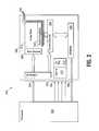
- FIG. 2details a system with a memory device in accordance with embodiments of the present invention.
- FIGS. 3A and 3Bdetail NOR and NAND architecture memory arrays in accordance with embodiments of the present invention.
- Non-volatile memory devices and arraysfacilitate the utilization of back-side trapped floating node memory cells with band-gap engineered gate and gate-insulator stacks with asymmetric tunnel barriers.
- Embodiments of the present inventionallow a separate front gate-insulator stack for reading and a separated back gate for programming (write and erase) and a back-side gate-insulator stack for charge storage. Additionally, the embodiments of the present invention allow implementation of the non-volatile memory device on bulk silicon and SOI or SON substrates with thick and thin channel regions/floating bodies formed between the front and back-side gate-insulator stacks (also known as the top or bottom gate-insulator stacks).
- Embodiments of the present inventionfurther allow for direct tunnel programming and efficient erase with electrons and holes in back-side trap memory cells, while maintaining high charge blocking barriers and deep carrier trapping sites for good charge retention and reduces the possibility of damage to the channel/insulator interface.
- the direct tunneling program and efficient erase capabilityreduces damage to the back gate-insulator stack and the crystal lattice from high energy carriers, reducing write fatigue and leakage issues and enhancing device lifespan.
- Utilizing the separate front side gate for reading the back-side trap memory cellsalso enable further scaling of device features with improved lithography through increased logic window, decreased susceptibility to short channel effect, and increased operational speed.
- Memory device embodiments of the present inventionare presented that are arranged in NOR or NAND memory architecture arrays. Memory cell embodiments of the present invention also allow multiple levels of bit storage in a single memory cell, and allow for programming and erase with reduced voltages, enhancing endurance and reducing power.
- source and drain regionsare formed and are separated by a thin or thick body channel region with a first gate stack (also known as the front gate stack, top gate stack, or access gate stack) formed over the channel region and/or portions of the source and drain regions.
- the top gate stackcomprises a layer of trap-free insulation and a control gate (the access gate) forming a FET device which allows for the formation of minority carriers in the channel and control of the carrier flow from the source to the drain through the channel via the voltage applied to the access gate.
- This top gate FETis typically used exclusively for sensing (reading) the state of the memory cell.
- a second gate-insulator stack(known as the back-side gate stack, bottom gate stack, or trapping layer gate stack) is formed beneath the channel region and is employed for charge storage and programming (writing and erasing).
- This device elementtypically comprises successive layers of tunnel insulation, a floating node trapping layer (or, alternatively, a conductive floating gate), a charge blocking insulation layer and a back-side control gate.
- This second gate stackwith its electrically isolated trapping layer, allows charge to be trapped beneath the channel region and affect the threshold voltage level of the sensing part (top gate FET) of the memory cell.
- the back-side control gatecan be formed of aluminum, tungsten, polysilicon or other conductor material and be independently coupled to a control line or, as is in the case of an SOI or bulk implementation, be formed from the substrate.
- Such back-side trap non-volatile memory cell FETsare also referred to as a vertically integrated “dual gate transistor non-volatile memory devices.”
- Conventional SONOS memory cell devicestypically employ successive layers of oxide/nitride/oxide (ONO) as the insulator stack between the silicon substrate and the heavily doped polysilicon control gate (or metal gate).
- the oxide adjacent to the silicon substrateis usually thinner and acts as a tunnel insulation layer (also known as a tunnel oxide) while the thicker oxide adjacent to the control gate acts as the charge blocking oxide. Trapped charges stored in the device are typically held at the tunnel oxide-nitride interface and at the bulk trapping centers in the nitride layer.
- the equivalent oxide thickness (EOT) of the SONOS memory cell gate-insulator stacktypically determines the program and erase voltage levels of the device. The program/erase speed, and especially, the erase speed and charge retention are strongly influenced by the tunnel oxide thickness.
- the logic window between the logic “1” and the logic “0” memory states(Vt“1” ⁇ Vt“0”) is generally dependent on the trapped charge density at the interface and in the bulk of the nitride and consequently increases with increasing thickness of the nitride. Due to the high field requirements of the charge transport through the tunnel oxide and the relatively low density of deep energy traps in the nitride, the a) voltage scalability, b) program/erase speed, and c) magnitude of the logic window are generally limited with the SONOS device ONO insulator stack when an industry standard minimum of ten years of charge retention is required. This is especially true if programming voltage levels are to be scaled.
- Floating gate memory cellsare even more limited in voltage scalability and speed compared to SONOS. This is due to the fact that the EOT of such device gate-insulator stacks are required to be nearly twice that of a SONOS device and the tunnel oxide thickness is two to four times as thick when compared to those of the SONOS device to be able to ensure ten years of charge retention.
- Floating gate Flash devicestypically employ oxide as the tunnel layer media and a thicker ONO stack on top of the polysilicon floating gate as the charge blocking layer.
- the control gateacts as both the “read” or “addressing” gate and the gate that controls the operation of programming and erase.
- “read” operationconductance of the memory cell FET determines the read speed of the device, which in turn typically depends on the transconductance and channel width/length (W/L) ratio of the device.
- W/Lchannel width/length
- device leakagedepends on short channel effects and the stability of the memory states. High voltage requirements and hot carrier induced degradation of tunnel oxide adversely affect read speed and read disturb, as well as device leakage, as mentioned above.
- the devicesbegin to be adversely affected by what has been called the short channel length effect.
- the short channel length effectAs the channel is reduced in length, the distance between the source and drain regions is decreased and the impurity diffusions that form the source and drain regions begin to merge under the device in the channel region. This has the effect of changing the device into a depletion mode device, where a channel of minority carriers is already formed in the channel region under the device and the device conducts current without the application of a voltage on the control gate. This leakage current through unselected devices can corrupt data reads on the common bitlines unless the device is isolated or driven with a voltage to force it to turn off.
- the short channel effectcan progress to the point where the device cannot be shut off, destroying the ability of the control gate to modulate the conductance of the device (it acts more and more as a resistor) and destroying it as a non-linear device.
- the short channel effectis typically not seen in dual gated transistors and back-side trap memory cell FETs, due to the thin channel body of the device and incident top and bottom fields.
- both the high voltage requirements and higher leakage currents associated with the programming (write/erase) of the current generation of flash technologyhave begun to adversely affect endurance, reliability, power and speed of operation of the resulting devices and limit scalability.
- the high programming and erase voltagesapply high fields across the gate insulator stack typically cause gate insulator oxide degradation. This gate insulator oxide degradation impacts device non-volatility (charge retention) and limits the overall device endurance (the number of program/erase cycles possible before failure). The high fields also severely limit the amount the device feature geometry can shrink beyond the current generation due to insulation and design requirements.
- the high programming voltagesare also known to induce a strong capacitive cross-coupling between a selected bit and adjacent unselected bits with the same wordline (or bitline) or between adjacent wordlines or bitlines.
- This cross-couplinghas become a critical issue in the overall memory device speed and scaling.
- Cross-coupling issuestypically increase as voltage levels are increased or as the memory device features are scaled smaller without there being a commensurate reduction in voltage levels.
- typical SONOS floating node memory cell devicesunlike floating gate devices, hold charges in discrete traps associated with a nitride trapping layer.
- the equivalent EOT of the central ONO insulator stack for such devicescan be as low as about half that of floating gate device and, therefore, the programming voltage level for a SONOS device is about half of that of an equivalent floating gate device.
- further voltage and feature scaling for SONOS devicesare limited without it adversely affecting charge retention (due to leakage and back-tunneling) and speed (which is typically tunnel oxide thickness dependent) and logic window (which is typically nitride trapping layer thickness dependent).
- Even though SONOS devicesmay operate by tunneling for both write and erase, the peak field across the tunnel oxide can still be very high (typically 10 MV/cm) causing the associated high field degradation of the tunnel oxide, adversely affecting endurance and reliability.
- oxide-based non-volatile memory cell devicessuch as traditional Flash, SONOS, or Nano-crystal memory cells are limited in voltage, power, speed, and feature scalability. Additionally, because of the high fields required across the oxide insulation layers, such oxide-based devices are also limited in reliability and endurance.
- Dual gate and Back-side trap devicesbecause of their structure, sandwich a (typically thin) body region between two gate stacks (the top and bottom gate stacks). This thin body transistor structure prevents short channel effect by limiting the channel body thickness and the available body charge.
- dual gate deviceshave been utilized in fast logic devices because of their improved channel conductance (due to twin minority channel carrier regions being formed at both the top and bottom of the channel body). and reduced capacitance thereby enhancing switching characteristics. As a result of these properties, dual gate and back-side trap devices can typically be scaled further while exhibiting better performance characteristics than single gate devices.
- Back-side trap memory cell embodiments of the present inventionutilize band-gap engineered gate-stacks that allow low voltage program and erase of the memory cells via the direct tunneling of carriers to or from the trapping layer held below the channel in the bottom gate stack.
- the band-gap engineered bottom gate stack of embodiments of the present inventionincorporate tunnel insulator layers having asymmetric tunnel barriers and one or more layers of direct tunnel insulator layers of increasing conduction band offset (each following tunnel layer has a higher conduction band energy level than the previous layer) and increasing values of K (dielectric constant) to provide very high electron current density during programming at reduced voltage drop across the direct tunnel layers.
- Kdielectric constant
- appropriate selections of charge trapping material and embedded nanocrystalsfacilitate a desired Vt shift for minimum adequate logical state/logical window separation.
- the dielectric constant values of the gate stack layershelp minimize the EOT of the gate insulator stack. This enables a gate stack EOT in the range of 2 nm to 6 nm to allow for low voltage operation and speed.
- Such methods of direct tunnel programming and erasure utilizing band-gap engineered asymmetric tunnel layersare detailed in U.S.
- the gate-stack of the embodiments of the present inventionutilizes one or more layers of material that are band-gap engineered with increasing band-gap offsets and high K values to form an asymmetric band-gap tunnel insulator layer.
- This asymmetric band-gap tunnel insulator layeris very efficient in charge transport in one direction and yet becomes very retarded in the reverse transport direction, presenting a large barrier.
- the asymmetric band-gap tunnel insulator layerallows for a low voltage direct tunneling to the trapping layer of the device when a programming field is applied across it utilizing the stepped internal fields of the one or more band-gaps of the asymmetric band-gap tunnel insulator layers, while the same stepped band-gap offsets and high K dielectrics present a large band-gap and consequently large energy barrier to the charges so trapped to prevent back-tunneling and maintain the required long term charge retention.
- embodiments of the present inventionprovide a non-volatile memory cell having an insulator stack with a low overall EOT, allowing them to be operated at very low power and at low programming voltage.
- the low voltage program and/or erase operations of embodiments of the present inventionalso reduce damage in the material of the device due to the tunneling/injection of carriers through the insulator layers (the injected carriers are “cool” and never gain enough energy to affect the lattice or material bonds).
- embodiments of the present inventionallow for improved scaling by allowing the memory to employ smaller effective oxide thicknesses (EOT) and low voltage layout and design in the array and support circuitry of the resulting memory device.
- EOTeffective oxide thicknesses
- the band-gap engineered tunneling medium of embodiments of the present inventionconsists of one or more layers of direct tunnel layers of increasing conduction band offset and increasing values of K (dielectric constant) to provide very high electron current density during programming at reduced voltage drop across the direct tunnel layers, allowing for high speed, low power programming.
- the charge blocking layer and tunnel layer placementare positioned in the bottom gate-insulator stack such that the tunnel insulator is positioned below the channel body and located between it and the floating node/trapping layer, and the charge blocking layer is between the back-side gate/substrate and the trapping layer.
- charge transporttakes place primarily between the channel and the trapping layer (floating node) of the bottom gate stack during programming and erasure.
- the stepped band-gap arrangementfacilitates direct tunneling of electrons layer to layer from the channel to the trapping layer with a low applied field.
- a high K charge blocking layeris also integrated in the bottom gate-stack between the trapping layer and the back-side gate/substrate for one embodiment of the present invention to maintain low charge leakage to the back-side gate/substrate from the trapping layer.
- nano-crystalsare embedded in a trapping layer which contains deep high density traps to provide a large trapped charge density, enhancing logic level separation and increasing stored charge, while minimizing the adverse effects of coulomb blockade and quantum confinement.
- the use of deep traps and/or nano-crystalsfurther increase charge retention by providing deep quantum wells at the trapping layer, further increasing the potential barrier that the trapped charges must overcome to escape from the trapping layer or back-tunnel through.
- the front/access gateis active and asserts a field to generate a channel of minority carriers in the channel body region, operating the top gate stack as a conventional FET.
- the bottom gate stackis inactive during reads, aside from the field asserted by the charge trapped on the trapping layer on carriers in the channel.
- Programming the back-side trap memory cell embodiments of the present inventionis accomplished by providing a voltage across the channel to the back-side gate/substrate to apply a field across the one or more tunnel layers and induce direct tunneling of electrons from the channel to the trapping layer of the bottom gate stack.
- multi-bit memory cell programmingmultiple data bits are encoded into a memory cell usually via either multiple charge centroids stored in the trapping layer or by modulating the threshold voltage level to encode the stored data bits.
- threshold voltage modulated multi-bit storagealso known as multi-level cell (MLC) storage
- MLCmulti-level cell
- the memory cellis then read by sensing the threshold voltage the memory cell activates at.
- the voltageis applied between a selected source/drain region (with back-side trap memory cell operating with the selected source/drain region acting as a source and the second source/drain region acting as the drain) and the back-side gate/substrate, tunneling electrons to the trapping layer directly adjacent to the selected source/drain region.
- the memory cellis then read utilizing the access gate and top gate stack by reversing the operational function of the first and second source/drain regions (the selected source/drain region acting as the drain and the second source/drain region acting as the source).
- Erasure in back-side trap memory cell embodiments of the present inventionis also accomplished by direct tunneling of holes and by enhanced Fowler-Nordhiem tunneling of electrons from the trapping sites.
- a voltageis applied across the tunnel layers from the back-side gate/substrate to the channel, applying a field across the one or more tunnel layers and inducing direct tunneling of holes from the channel body and Fowler-Nordhiem tunneling of electrons from the trapping layer of the bottom gate-stack to erase the memory cell.
- the erasure operationis relatively slower than the corresponding direct tunnel program operation, due to the asymmetric tunnel barrier and/or the higher effective mass of holes.
- the relatively slower erasecan be offset by utilization of a block erase operation, where a large block of bits is erased in parallel.
- the erase speed of the back-side trap memory cell erasure of embodiments of the present inventioncan also be accomplished by or enhanced by a combination of conventional hot-hole injection, enhanced Fowler-Nordheim electron tunneling, or by enhanced Fowler-Nordhiem tunneling of holes from the back-side gate/substrate.
- This programming and erasure by the transport of electrons and holes by direct tunnelingallows embodiments of the present invention to consume orders of magnitude lower power compared to conventional flash memory cells and devices.
- Writing and erase speedare significantly enhanced as electrons and holes tunnel directly from one direct tunnel layer into the next through successive layers of low barrier energy.
- the tunnel insulation layer region of embodiments of the present inventionmay consist of one or more layers of dielectric material with increasing conduction band offsets and/or increasing dielectric K values, allowing directionally asymmetric direct tunneling efficiency of carriers through the tunnel layer.
- the layers of dielectric materialcan be selected from any commonly utilized insulator materials (oxides, mixed oxides, nitrides, oxynitrides, mixed oxynitrides, or silicates) so long as they are arranged in increasing band-gap offsets and, preferably, higher K dielectric materials to help reduce the EOT of the resulting memory cell.
- Examples of these insulator materialsinclude, but are not limited to, silicon dioxide (SiO 2 ), titanium dioxide (TiO 2 ), hafnium oxide (HfO 2 ), zirconium oxide, Praseodymium Oxide (Pr 2 O 3 ), alumina (Al 2 O 3 ), mixed oxide hafnium and aluminum, mixed oxide of hafnium and titanium, mixed oxide of hafnium and silicon, silicon oxynitride (SiON), SiN, AlN, HfN, mixed oxynitrides of hafnium and silicon, etc.
- These layers of increasing band-gap offset dielectric materialare typically deposited during manufacturing processing utilizing atomic layer deposition (ALD) or other appropriate deposition processes.
- SiNsilicon nitride
- a two-layer tunnel structurecan consist of SiO 2 /Pr 2 O 3 or SiO 2 /TiO 2 , SiO 2 /HfO 2 , etc. It is noted that other two, three, or more layer asymmetric band-gap tunnel regions of embodiments of the present invention are also possible and will be apparent to those skilled in the art with the benefit of the present disclosure, and as such the above examples should not be considered as limiting.
- the successive layers of the asymmetric band-gap tunnel layernot only have increasing band offsets, but also have material of higher K values and increased direct tunnel thickness to minimize the effective EOT of the tunnel layer composite and optimize voltage drop across the each of the tunnel layers.
- the physical thickness of the composite tunnel layercan be preferably designed to be around 3 nm or less and the EOT around 1.5 nm or less for low voltage operation.
- metal nano-crystal memory devicesthat contain certain metal or semiconductor nano-dots or nano-crystals including, but not limited to, tungsten, silicon, germanium, cobalt, platinum, gold, iridium, and palladium to provide deep energy trapping sites at the metal-insulator interface due to large work function difference.
- metal or semiconductor nano-dots or nano-crystalsincluding, but not limited to, tungsten, silicon, germanium, cobalt, platinum, gold, iridium, and palladium to provide deep energy trapping sites at the metal-insulator interface due to large work function difference.
- quantum confinement effectto prevent electrons from tunneling between adjacent trapping sites within the trapping layer or tunneling back to silicon.
- coulomb blockadewhere like charges repel each other could further degrade charge retention, such that, in design, multiple charge trapping per nano-dot should be avoided.
- the effective charge trapping density of nano-dot trapping layeris limited to around 1E12/cm 2 to 2E12/cm 2 regardless of the actual density of nano-dots. Consequently, the effective charge trapping density for conventional nano-dot or nano-crystal devices is limited.
- This effective charge trapping density limitationcan be overcome if a selected geometry and distribution of nano-crystals were embedded in insulating trapping layers that also contained a high density of naturally occurring deep traps, such as SiN, AlN, or SiON. If this trapping layer is also formed of high K material, the EOT of the entire bottom gate stack would also be reduced.
- silicon nitrideSi 3 N 4
- the trapping mediumis then embedded with nano-crystals/nano-dots that can include, but are not limited to tungsten, silicon, germanium, cobalt, platinum, iridium, gold, or palladium in sizes ranging from 1.5 nm to 4 nm with a separation of 3.5 nm to 5 nm to further increase the number of trapping sites.
- the silicon oxy-nitride (SiON) utilized in the above exampleprovides additional charge trapping sites.
- deep energy trapsare associated with larger concentrations of Si—O—N bond “defects” in the silicon oxy-nitrides.
- Such a trapping layer of an embodiment of the present inventionwould provide an effective charge density in the desired range of 5E12/cm 2 to 1E13/cm 2 without the adverse effects on retention due to coulomb blockade or quantum confinement. It is noted that other charge trapping insulator materials may also be utilized in embodiments of the present invention as the charge trapping layer.
- KK dielectric material layers
- insulatorscan be utilized in charge blocking layers of embodiments of the present invention, including, but not limited to insulators from the oxide, mixed oxide, nitride, oxynitrides, mixed oxynitrides, and silicate families.
- the access gate and back-side gate/substrate of embodiments of the present inventiontypically have a thin passivating conductive underlayer of HfN, TiN, IrO 2 or TaN (for process integration) over the gate or substrate.
- the access gate or back-side gate(if a separate material and not formed from the substrate) typically comprise either a polysilicon gate or any other appropriate metal gate (such as aluminum, iridium or tungsten) formed under the charge blocking layer of the bottom gate stack.
- FIGS. 1A and 1Bdetail physical cross sections of both a bulk silicon implementation 100 and a silicon-on-insulator (SOI) implementation 140 of the back-side trap non-volatile device structures, while FIG. 1E details the corresponding band-gap diagram of a back-side trap memory cell 100 , 140 in accordance with embodiments of the present invention.
- a bulk back-side gate NFET memory cell 100is shown formed on a substrate 102 .
- the memory cell 100has a first and second source/drain regions 104 , 106 , in contact with a thin or thick body channel region 108 .
- a top gate-stack 110is formed over the silicon body channel region 108 , containing an access gate 114 isolated from the body channel 108 by a gate insulator layer 116 .
- a bottom gate-stack 112is formed under the channel region 108 .
- the back-side control gate 122is formed as a bulk back-side control gate from the substrate 102 , which may either be a bulk or silicon-on-insulator (SOI) substrate.
- SOIsilicon-on-insulator
- the insulator stack 120 of the bottom gate-stack 112contains a charge blocking layer 124 formed over the bulk back-side control gate 122 , a trapping layer/floating gate 126 formed over the charge blocking layer 124 , and a tunnel insulator layer 118 formed over the trapping layer 126 , directly under the channel region 108 .
- the tunnel insulator layer 118includes one or more layers of materials layered to provide an asymmetric stepped band-gap profile.
- the trapping layer 126may also be optionally provided with deep traps and embedded metal nano-crystals.
- Multiple layers of single crystal semiconductor filmscan be deposited over bulk silicon substrate, as well as over SOI substrates.
- a layer of appropriate thickness germaniumcan be deposited over a silicon substrate to be followed be another layer of epitaxially grown silicon.
- selective localized voidscan be formed underneath the top silicon film.
- This techniquewas developed by M Jurezak et al. VLSI Tech. Digest p.29, 1999, and is called silicon-on-nothing or SON.
- Recently R. Ranica et al.built and characterized PMOS back-side trapped SONOS memories by depositing ONO layers on SON (R. Ranica et al., IEEE Silicon nanoelectronic workshop, p.99, 2004).
- the present inventionapplies similar techniques in bulk silicon and SOI to create novel back-side trapped non-volatile memory cells.
- a back-side non-volatile memory cellcomprises a first and second source/drain regions formed over the buried oxide (BOX) region of an SOI substrate.
- Top gate and underlying trap-free insulatoris formed over the thing-body p-type silicon similar to a fully depleted SOI-NFET device.
- Underneath the thin floating body, an ONO replacement back gate-insulator stack and the back gateis formed between the thin body and the BOX region.
- the back gatemay consist of heavily doped N+ or P+ polysilicon or metal, while the ONO replacement layer consists of a charge blocking layer formed over the back gate, a trapping layer formed over the charge blocking layer, and one or more sub-layers of tunnel insulator formed over the trapping layer and interfacing the thin floating body.
- the back gate and the insulator stackare formed in a similar manner of silicon-on-nothing (SON) implementation as outlined by the reference of R. Ranica et al.
- the tunnel insulator layermay consist of one or more layers of dielectric material of increasing conduction band offset.
- a silicon-on-insulator (SOI) back-side gate NFET memory cell 140is shown formed on a substrate 142 utilizing a silicon-on-nothing (SON) design.
- Silicon-on-nothing (SON) designforms a void 164 under the body of the device to reduce the effect of substrate parasitics on the resulting circuit element.
- the memory cell 140has a first and second source/drain regions 144 , 146 , in contact with a floating body channel region 148 .
- a top gate-stack 150is formed over the channel region 148 , containing an access gate 154 isolated from the channel by an insulator layer 156 .
- a bottom gate-insulator stack 152is formed under the floating body region 148 .
- the bottom gate-insulator stack 152contains a charge blocking layer 162 formed over a back-side gate 166 , a trapping layer 160 formed over the charge blocking layer 162 .
- a multi-layer asymmetric band-gap tunnel insulator layer 158is formed over the trapping layer 160 , directly under the channel region 148 .
- the tunnel insulator layer 158includes two or more layers of materials layered to provide an asymmetric stepped band-gap profile.
- the trapping layer 160may also be optionally provided with deep traps and embedded metal nano-crystals.
- FIG. 1Cillustrates an example of an ONO replacement gate-insulator stack for the bottom gate-insulator stack 120 , 152 of an embodiment of the present invention.
- FIG. 1Dillustrates the details of a relatively more complex example of a bottom gate-insulator stack 120 , 152 of an embodiment of the present invention containing tunnel dielectric medium 118 , 158 , a more complex trapping medium 126 , 160 , and a high-K charge blocking medium 124 , 162 .
- the tunnel media 118 , 158consists of two or more layers of dielectric of increasing conduction band offset and high K values, enabling direct tunnel “barrier thinning” (a shorter effective tunnel distance when field is imposed across the tunnel insulator layer) thereby promoting significantly enhanced electron transport across the layers at reduced fields.
- the trapping media 126 , 160consists of a high K dielectric layer of intrinsic deep traps of high trap density, aided by enhanced trapping due to embedded high work function nano-dots.
- the EOT of an equivalent gate-insulator stackcan be reduced by 30% or more compared to an ONO gate-stack and correspondingly lowers the programming voltage levels.
- ONO replacementmay be considered for the bottom gate-insulator stack 120 , 152 , to achieve (a) a lower EOT of the insulator stack, thereby achieving voltage scaling; (b) band engineered asymmetric direct tunneling for electrons and holes to achieve low voltage, low energy high speed carrier transport to the trapping sites and reduce back tunneling of carriers; (c) high density deep energy trapping material to achieve retention and logic window; and (d) high K, large band-gap charge blocking insulator with high barrier energy for electrons and holes, to prevent back injection and charge loss.
- high K insulatorsare desired to reduce the incident field, thereby improving stack reliability.
- Direct tunnelingis enhanced by reducing tunneling distance (“barrier thinning”) and by reducing barrier energy while the later enhances Fowler-Nordhiem tunneling. Specific examples of which are detailed herein, in the various embodiments of the present invention.
- the back-side gate 166(in embodiments with separate back-side gates) is then typically formed of polysilicon, tungsten, iridium, or aluminum and may include an initial passivation layer, such as a thin layer of HfN, TaN, TiN, or IrO 2 formed under the charge blocking layer 124 , 162 .
- the effective oxide thickness (EOT) of these three layerscould be as low as 1.32 nm.
- the trapping layer 126 , 160is formed of a layer of 6 nm of HfO 2 with 3.5-4.0 nm of embedded Cobalt nano-dots, having a resulting EOT of 0.3 nm.
- the back-side gate electrode 166formed of 10 nm of TiN as a passivation layer and doped polysilicon.
- insulatorscan be utilized in embodiments of the present invention, including, but not limited to insulators from the oxide, mixed oxide, nitride, oxynitride, mixed oxynitride, and silicate families.
- FIG. 1Edetails a band-gap diagram 170 of a back-side trap memory cell 100 , 140 of FIGS. 1A and 1B in accordance with embodiment of the present invention.
- the access gate 114 , 154is separated from the body/channel 108 , 148 by the access gate insulator layer 116 , 156 .
- the trapping layer 126 , 160is separated from the channel 108 , 148 by the one or more layers of the asymmetric band-gap tunnel layer 118 , 158 , and from the back-side gate 166 /substrate 102 by the charge blocking layer 124 , 162 .
- FIG. 2shows a simplified diagram of a system 228 incorporating a non-volatile memory device 200 of the present invention coupled to a host 202 , which is typically a processing device or memory controller.
- the non-volatile memory 200is a NOR architecture Flash memory device or a NAND architecture Flash memory device.
- the non-volatile memory device 200has an interface 230 that contains an address interface 204 , control interface 206 , and data interface 208 that are each coupled to the processing device 202 to allow memory read and write accesses. It is noted that other memory interfaces 230 that can be utilized with embodiments of the present invention exist, such as a combined address/data bus, and will be apparent to those skilled in the art with the benefit of the present disclosure.
- the interface 230is a synchronous memory interface, such as a SDRAM or DDR-SDRAM interface.
- an internal memory controller 210directs the internal operation; managing the non-volatile memory array 212 and updating RAM control registers and non-volatile erase block management registers 214 .
- the RAM control registers and tables 214are utilized by the internal memory controller 210 during operation of the non-volatile memory device 200 .
- the non-volatile memory array 212contains a sequence of memory banks or segments 216 . Each bank 216 is organized logically into a series of erase blocks (not shown).
- Memory access addressesare received on the address interface 204 of the non-volatile memory device 200 and divided into a row and column address portions.
- the non-volatile memory 200is utilized by the host 202 as a universal or ideal memory, replacing both the RAM and ROM in the system 228 .
- row decode circuit 220On a read access the row address is latched and decoded by row decode circuit 220 , which selects and activates a row/page (not shown) of memory cells across a selected memory bank.
- the bit values encoded in the output of the selected row of memory cellsare coupled to a local bit line (not shown) and a global bit line (not shown) and are detected by sense amplifiers 222 associated with the memory bank.
- the column address of the accessis latched and decoded by the column decode circuit 224 .
- the output of the column decode circuit 224selects the desired column data from the internal data bus (not shown) that is coupled to the outputs of the individual read sense amplifiers 222 and couples them to an I/O buffer 226 for transfer from the memory device 200 through the data interface 208 .
- the row decode circuit 220selects the row page and column decode circuit 224 selects write sense amplifiers 222 .
- Data values to be writtenare coupled from the I/O buffer 226 via the internal data bus to the write sense amplifiers 222 selected by the column decode circuit 224 and written to the selected non-volatile memory cells (not shown) of the memory array 212 .
- the written cellsare then reselected by the row and column decode circuits 220 , 224 and sense amplifiers 222 so that they can be read to verify that the correct values have been programmed into the selected memory cells.
- the two common types of EEPROM and Flash memory array architecturesare the “NAND” and “NOR” architectures, so called for the similarity each basic memory cell configuration has to the corresponding logic gate design.
- the non-volatile memory cells of the memory arrayare arranged in a matrix similar to RAM or ROM.
- the access gates of each non-volatile memory cell of the array matrixare coupled by rows to word select lines (word lines) and their drains are coupled to column bit lines.
- the source of each non-volatile memory cellis typically coupled to a common source line.
- the NOR architecture non-volatile memory arrayis accessed by a row decoder activating a row of non-volatile memory cells by selecting the word line coupled to their access gates.
- the row of selected memory cellsthen place their stored data values on the column bit lines by flowing a differing current from the coupled source line to the coupled column bit lines depending on their programmed states.
- a column page of bit linesis selected and sensed, and individual data words are selected from the sensed data words from the column page and communicated from the memory.
- a NAND array architecturealso arranges its array of non-volatile memory cells in a matrix such that the access gates of each non-volatile memory cell of the array are coupled by rows to word lines.
- each memory cellis not directly coupled to a source line and a column bit line.
- the memory cells of the arrayare arranged together in strings, typically of 8, 16, 32, or more each, where the memory cells in the string are coupled together in series, source to drain, between a common source line and a column bit line. This allows a NAND array architecture to have a higher memory cell density than a comparable NOR array, but with the cost of a generally slower access rate and programming complexity.
- a NAND architecture non-volatile memory arrayis accessed by a row decoder activating a row of non-volatile memory cells by selecting the word select line coupled to their access gates.
- the word lines coupled to the access gates of the unselected memory cells of each stringare also driven.
- the unselected memory cells of each stringare typically driven by a higher access gate voltage so as to operate them as pass transistors and allowing them to pass current in a manner that is unrestricted by their stored data values.
- Currentthen flows from the source line to the column bit line through each non-volatile memory cell of the series coupled string, restricted only by the memory cells of each string that are selected to be read. This places the current encoded stored data values of the row of selected memory cells on the column bit lines.
- a column page of bit linesis selected and sensed, and then individual data words are selected from the sensed data words from the column page and communicated from the memory device.
- FIG. 3Ashows a simplified NOR back-side trap floating node/trapping layer memory array 300 of a EEPROM or Flash memory device of an embodiment of the present invention.
- a NOR array 300couples back-side trap memory cells 302 of embodiments of the present invention to bit lines 312 , source lines 314 , word lines 306 , and a substrate connection 222 .
- the bit lines 312 and source lines 314are typically formed locally from N+ doped regions deposited in the substrate and are separated by a channel region.
- Each memory cell FET 302has a top gate-insulator stack formed over the channel region and a bottom gate-insulator stack formed under the channel region and between the N+ doped regions of a bit line 312 and a source line 314 , utilizing the N+ doped regions as a drain and source respectively (it is noted that the source line 314 may be replaced with a second bit line 312 connection in multi-bit cell arrays, so that the current flow through the memory cell may be reversed).
- the bottom gate-insulator stackis made of an asymmetric band-gap tunnel insulator layer having one or more layers formed beneath the channel region, a floating node/trapping layer formed under the tunnel insulator, charge blocking insulator layer formed under the trapping layer, and a back-side gate formed under the charge blocking insulator. It is noted that in another embodiment of the present invention, the substrate takes the place and function of the back-side gate, which is then not individually formed.
- the top gate-insulator stackis made of an insulator layer formed on top of the channel region and an access gate 306 (typically formed integral to the word line 306 , also known as a control gate line) formed over the insulator.
- an access gate 306typically formed integral to the word line 306 , also known as a control gate line
- back-side gate control lines 316are shown coupled to the back-side gates of each row, allowing the memory cells of the row to be programmed and erased. It is noted that, instead of individual back-side gate control lines 316 , the substrate connection 322 can be utilized to apply programming and erase voltages to the back-side gate, in particular, where the back-side gate is formed by the substrate. To further enable this mode of operation, in one embodiment of the present invention, each row of memory is formed in isolation trenches, allowing the substrate of each isolation trench to be individually biased. It is also noted that other NOR architecture memory array 300 configurations incorporating embodiments of the present invention are possible and will be apparent to those skilled in the art with the benefit of the present disclosure.
- FIG. 3Bdetails a simplified NAND memory string 320 of a NAND architecture EEPROM or Flash memory device of an embodiment of the present invention.
- a series of back-side trap memory cells 302 of embodiments of the present inventionare coupled together source to drain to form a NAND string 320 (typically of 8, 16, 32, or more cells).
- Each memory cell FET 302has a top gate-insulator stack formed over the channel region and a bottom gate-insulator stack formed under the channel region. N+ doped regions are formed between each gate insulator stack to form the source and drain regions of the adjacent floating node memory cells, which additionally operate as connectors to couple the cells of the NAND string 320 together.
- Optional select gates 304that are coupled to gate select lines, are formed at either end of the NAND floating node string 320 and selectively couple opposite ends of the NAND floating node string 320 to a bit line 312 and a source line 314 .
- the NAND architecture memory string 320 of FIG. 3Bwould be coupled to bit lines 312 , source lines 314 , word lines 306 , and a substrate connection 322 .
- the bottom gate-insulator stackis made of an asymmetric band-gap tunnel insulator layer having one or more layers formed beneath the channel region, a floating node/trapping layer formed under the tunnel insulator, charge blocking insulator layer formed under the trapping layer on top of the substrate, which takes the place and function of the back-side gate.
- each NAND architecture memory string 320 of memoryis formed in an isolation trench, allowing the substrate of each isolation trench to be individually biased for programming and erasure.
- an individual back-side gatecan be formed under the charge blocking insulator and coupled to a back-side gate control line.
- the top gate-insulator stackis made of an insulator layer formed on top of the channel region and an access gate 306 (typically formed integral to the word line 306 , also known as a control gate line) formed over the insulator.
- the substrate connection 322is shown coupled to the back-side gates of each NAND string 320 , allowing the memory cells of each NAND string 320 to be programmed and erased. It is noted that, as described above, instead of utilizing the substrate connection 322 , individual back-side gate control lines can be formed and utilized to apply programming and erase voltages to a formed back-side gate.
- Non-volatile memory devices and arrayshave been described that utilize back-side trapped floating node memory cells with band-gap engineered back-side gate-insulator stacks with asymmetric tunnel barriers.
- Embodiments of the present inventionallow for direct tunnel programming and efficient erase with electrons and holes, while maintaining high charge blocking barriers and deep carrier trapping sites for good charge retention and reduces the possibility of damage to the channel/insulator interface by separating sensing from programming via a front side FET element of the memory device.
- the direct tunneling program and efficient erase capabilityreduces damage to the back-side gate stack and enhances device endurance and reliability.
- Back-side trap memory cellsalso enable scaling of feature size due to voltage scalability and elimination of short channel effect via a thin body channel device.
- Memory device embodiments of the present inventionare presented that are arranged in NOR or NAND memory architecture arrays. Memory cell embodiments of the present invention also allow multiple levels of bit storage in a single memory cell, and allow for programming and erase with reduced voltages.
Landscapes
- Engineering & Computer Science (AREA)
- Chemical & Material Sciences (AREA)
- Nanotechnology (AREA)
- Physics & Mathematics (AREA)
- Mathematical Physics (AREA)
- Theoretical Computer Science (AREA)
- Crystallography & Structural Chemistry (AREA)
- Non-Volatile Memory (AREA)
- Semiconductor Memories (AREA)
Abstract
Description
- The present invention relates generally to integrated circuits and in particular the present invention relates to non-volatile memory devices.
- Memory devices are typically provided as internal storage areas in the computer. The term memory identifies data storage that comes in the form of integrated circuit chips. There are several different types of memory used in modem electronics, one common type is RAM (random-access memory). RAM is characteristically found in use as main memory in a computer environment. RAM functions as a read and write memory; that is, you can both write data into RAM and read data from RAM. This is in contrast to read-only memory (ROM), which permits you only to read data. Most RAM is volatile, which means that it requires a steady flow of electricity to maintain its contents. As soon as the power is turned off, whatever data was in RAM is lost.
- Computers almost always contain a small amount of ROM that holds instructions for starting up the computer. Unlike RAM, ROM cannot be written to. An EEPROM (electrically erasable programmable read-only memory) is a special type non-volatile ROM that can be erased by exposing it to an electrical charge. EEPROM comprise a memory array which includes a large number of memory cells having electrically isolated gates. Data is stored in the memory cells in the form of charge on the floating gates or floating nodes associated with the gates. Each of the cells within an EEPROM memory array can be electrically programmed in a random basis by charging the floating node. The charge can also be randomly removed from the floating node by an erase operation. Charge is transported to or removed from the individual floating nodes by specialized programming and erase operations, respectively.
- Yet another type of non-volatile memory is a Flash memory. A Flash memory is a type of EEPROM that is typically erased and reprogrammed in blocks instead of a single bit or one byte (8 or 9 bits) at a time. A typical Flash memory comprises a memory array, which includes a large number of memory cells. Each of the memory cells includes a floating gate field-effect transistor (FET) capable of holding a charge. The data in a cell is determined by the presence or absence of the charge in the floating gate/charge trapping layer. The cells are usually grouped into sections called “erase blocks.” Each of the cells within an erase block can be electrically programmed in a random basis by charging the floating gate. The charge can be removed from the floating gate by a block erase operation, wherein all floating gate memory cells in the erase block are erased in a single operation.
- The memory cells of both an EEPROM memory array and a Flash memory array are typically arranged into either a “NOR” architecture (each cell directly coupled to a bit line) or a “NAND” architecture (cells coupled into “strings” of cells, such that each cell is coupled indirectly to a bit line and requires activating the other cells of the string for access).
- Floating gate memory cells are typically programmed by injecting electrons to the floating gate by channel hot carrier injection (CHE), typically placing the cell in a high threshold voltage state. Floating gate memory cells can also be erased by hot hole injection from the substrate. Alternatively, floating gate memory cells can be programmed and erased by electron tunneling to and from the substrate by Fowler-Nordheim tunneling to put the cell in a programmed or erased threshold state. Both mechanisms require the generation of high positive and negative voltages in the memory device and can place high fields across the gate insulation layers with resulting adverse effects in device characteristics and reliability.
- A problem with CHE, hot hole injection and Fowler-Nordheim tunneling is that the high energy required for their operation damages the oxide interfacing silicon substrate, reducing memory cell retention, endurance, and degrading transconductance of the FET. In particular, the tunnel insulation layer, which is placed between the channel and the floating node/charge trapping layer is typically damaged by the programming process by having hot carriers injected or tunneled through it. As high control fields are also typically asserted on the channel during writing and erasing through the tunnel insulation layer by the application of voltage to the control gate of the memory cell, damage to the tunnel insulator by the hot carrier injection or high fluence tunneling process can significantly affect device characteristics. Hot carrier injection can generate interface states, degrade device transconductance, and enhance device leakage via enhanced short channel effect, besides affecting charge retention and read-disturb. Hot hole injection can generate fixed charge trapping centers in the tunneling insulators and associated defects in the trapping layer, thus breaking stable bonds and eventually degrading the insulator/dielectric properties of the device. For a conventional Flash or SONOS non-volatile memory device, the same control gate is also used during a read operation as a FET to read the state of the memory cell. When the tunnel insulator (also known as the tunnel oxide) is degraded, the read characteristics of the memory cell are also degraded due to the transconductance degradation and enhanced leakage. This affects the read speed of the memory cell.
- An additional problem in Flash and SONOS memory cell arrays is that voltage scalability affects the minimum cell size, and consequently the overall memory density of any resulting array. As integrated circuit processing techniques improve, manufacturers try to reduce the feature sizes of the devices produced and thus increase the density of the IC circuits and memory arrays. In modem IC circuits and memory arrays, as SONOS transistors and floating gate memory cells are scaled to smaller feature sizes, the device characteristics of the component transistors and floating gate memory cells can alter and leave the resulting IC or memory device non-functional. These issues include, but are not limited to, short channel effect, signal cross-talk, device programming and operating voltages, reduced logic windows, oxide punch-through, and charge leakage and retention.
- For the reasons stated above, and for other reasons stated below which will become apparent to those skilled in the art upon reading and understanding the present specification, there is a need in the art for methods and apparatus for a non-volatile memory cell that allows for feature and voltage scaling, prevents read degradation while providing enhanced retention, speed, endurance, and exhibits increased device integrity.
- The above-mentioned problems with producing a non-volatile memory cell that allows for increased device feature scaling with low voltage programming and efficient erasure with high charge retention, enhanced speed and reliability and other problems are addressed by the present invention and will be understood by reading and studying the following specification.
- Non-volatile memory devices and arrays, in accordance with embodiments of the present invention, utilize back-side trapped floating node memory cells with band-gap engineered back-side gate stacks with asymmetric or direct tunnel barriers that allow for low voltage tunneling programming and efficient erase with electrons and holes, while maintaining high charge blocking barriers and deep carrier trapping sites for good charge retention. The front gate interfaces with a standard gate dielectric (such as SiO2or, optionally, a trap free alternate gate dielectric) to achieve a fixed threshold field effect transistor in the top gate-insulator stack and is exclusively employed for reading the memory state held in the back-side gate-insulator stack of the device. Since reading is a low field operation, front gate insulator integrity and FET transconductance are preserved and read speed is maintained. Read disturb and device leakage are eliminated for the same reason. Back-side trap memory cells also enable further scaling of device features with progressive lithographic and feature size scaling. Memory device embodiments of the present invention are presented that are arranged in NOR or NAND memory architecture arrays. Memory cell embodiments of the present invention also allow multiple levels of bit storage in a single memory cell, and allow for programming and erase with reduced voltages.
- For one embodiment, the invention provides a back-side trap non-volatile memory cell comprising a first and second source/drain regions coupled by a channel region, a top gate-stack, containing an access gate insulator layer formed over the channel region and an access gate formed over the access gate insulator layer, and a bottom gate-stack. The bottom gate-stack comprises a back-side gate, a charge blocking layer formed over the back-side gate, a trapping layer formed over the charge blocking layer, and a single direct tunnel insulator layer or an asymmetric band-gap tunnel insulator layer containing two or more sub-layers formed over the trapping layer and beneath the channel region, wherein the two or more sub-layers comprise layers of increasing conduction band offset.
- For another embodiment, the invention provides a non-volatile memory device comprising a memory interface, a control circuit coupled to the memory interface, and a non-volatile memory array containing a plurality of back-side trap non-volatile memory cells formed into rows and columns. One or more of the plurality of back-side trap non-volatile memory cells comprise a first and second source/drain regions coupled by a channel region, a top gate-stack, containing an access gate insulator layer formed over the channel region and an access gate formed over the access gate insulator layer, and a bottom gate-stack. The bottom gate-stack comprises a back-side gate, a charge blocking layer formed over the back-side gate, a trapping layer formed over the charge blocking layer, and an asymmetric band-gap tunnel insulator layer containing one or more sub-layers formed over the trapping layer and beneath the channel region, wherein the one or more sub-layers comprise layers of increasing conduction band offset with the trapping layer.
- Other embodiments are also described and claimed.
FIGS. 1A-1E detail bulk and SOI back-side trap memory cells and band diagram in accordance with embodiments of the present invention.FIG. 2 details a system with a memory device in accordance with embodiments of the present invention.FIGS. 3A and 3B detail NOR and NAND architecture memory arrays in accordance with embodiments of the present invention.- In the following detailed description of the preferred embodiments, reference is made to the accompanying drawings that form a part hereof, and in which is shown by way of illustration specific preferred embodiments in which the inventions may be practiced. These embodiments are described in sufficient detail to enable those skilled in the art to practice the invention, and it is to be understood that other embodiments may be utilized and that logical, mechanical and electrical changes may be made without departing from the spirit and scope of the present invention. The terms wafer and substrate used previously and in the following description include any base semiconductor structure. Both are to be understood as including bulk substrate, silicon-on-sapphire (SOS) technology, silicon-on-insulator (SOI) technology, silicon-on-nothing (SON) technology, thin film transistor (TFT) technology, doped and undoped semiconductors, epitaxial layers of silicon supported by a base semiconductor, as well as other semiconductor structures well known to one skilled in the art. Furthermore, when reference is made to a wafer or substrate in the following description, previous process steps may have been utilized to form regions/junctions in the base semiconductor structure. The following detailed description is, therefore, not to be taken in a limiting sense, and the scope of the present invention is defined only by the claims and equivalents thereof.
- Non-volatile memory devices and arrays, in accordance with embodiments of the present invention, facilitate the utilization of back-side trapped floating node memory cells with band-gap engineered gate and gate-insulator stacks with asymmetric tunnel barriers. Embodiments of the present invention allow a separate front gate-insulator stack for reading and a separated back gate for programming (write and erase) and a back-side gate-insulator stack for charge storage. Additionally, the embodiments of the present invention allow implementation of the non-volatile memory device on bulk silicon and SOI or SON substrates with thick and thin channel regions/floating bodies formed between the front and back-side gate-insulator stacks (also known as the top or bottom gate-insulator stacks). Embodiments of the present invention further allow for direct tunnel programming and efficient erase with electrons and holes in back-side trap memory cells, while maintaining high charge blocking barriers and deep carrier trapping sites for good charge retention and reduces the possibility of damage to the channel/insulator interface. The direct tunneling program and efficient erase capability reduces damage to the back gate-insulator stack and the crystal lattice from high energy carriers, reducing write fatigue and leakage issues and enhancing device lifespan. Utilizing the separate front side gate for reading the back-side trap memory cells also enable further scaling of device features with improved lithography through increased logic window, decreased susceptibility to short channel effect, and increased operational speed. Memory device embodiments of the present invention are presented that are arranged in NOR or NAND memory architecture arrays. Memory cell embodiments of the present invention also allow multiple levels of bit storage in a single memory cell, and allow for programming and erase with reduced voltages, enhancing endurance and reducing power.
- In back-side trap non-volatile memory cell FETs, source and drain regions are formed and are separated by a thin or thick body channel region with a first gate stack (also known as the front gate stack, top gate stack, or access gate stack) formed over the channel region and/or portions of the source and drain regions. The top gate stack comprises a layer of trap-free insulation and a control gate (the access gate) forming a FET device which allows for the formation of minority carriers in the channel and control of the carrier flow from the source to the drain through the channel via the voltage applied to the access gate. This top gate FET is typically used exclusively for sensing (reading) the state of the memory cell. A second gate-insulator stack (known as the back-side gate stack, bottom gate stack, or trapping layer gate stack) is formed beneath the channel region and is employed for charge storage and programming (writing and erasing). This device element typically comprises successive layers of tunnel insulation, a floating node trapping layer (or, alternatively, a conductive floating gate), a charge blocking insulation layer and a back-side control gate. This second gate stack, with its electrically isolated trapping layer, allows charge to be trapped beneath the channel region and affect the threshold voltage level of the sensing part (top gate FET) of the memory cell. The back-side control gate can be formed of aluminum, tungsten, polysilicon or other conductor material and be independently coupled to a control line or, as is in the case of an SOI or bulk implementation, be formed from the substrate. Such back-side trap non-volatile memory cell FETs are also referred to as a vertically integrated “dual gate transistor non-volatile memory devices.”
- Conventional SONOS memory cell devices typically employ successive layers of oxide/nitride/oxide (ONO) as the insulator stack between the silicon substrate and the heavily doped polysilicon control gate (or metal gate). The oxide adjacent to the silicon substrate is usually thinner and acts as a tunnel insulation layer (also known as a tunnel oxide) while the thicker oxide adjacent to the control gate acts as the charge blocking oxide. Trapped charges stored in the device are typically held at the tunnel oxide-nitride interface and at the bulk trapping centers in the nitride layer. The equivalent oxide thickness (EOT) of the SONOS memory cell gate-insulator stack typically determines the program and erase voltage levels of the device. The program/erase speed, and especially, the erase speed and charge retention are strongly influenced by the tunnel oxide thickness. The logic window between the logic “1” and the logic “0” memory states (Vt“1”−Vt“0”) is generally dependent on the trapped charge density at the interface and in the bulk of the nitride and consequently increases with increasing thickness of the nitride. Due to the high field requirements of the charge transport through the tunnel oxide and the relatively low density of deep energy traps in the nitride, the a) voltage scalability, b) program/erase speed, and c) magnitude of the logic window are generally limited with the SONOS device ONO insulator stack when an industry standard minimum of ten years of charge retention is required. This is especially true if programming voltage levels are to be scaled.
- Regardless of the mechanisms of charge transport employed (CHE, Hot Hole, or Fowler-Nordheim Tunneling), Floating gate memory cells are even more limited in voltage scalability and speed compared to SONOS. This is due to the fact that the EOT of such device gate-insulator stacks are required to be nearly twice that of a SONOS device and the tunnel oxide thickness is two to four times as thick when compared to those of the SONOS device to be able to ensure ten years of charge retention. Floating gate Flash devices typically employ oxide as the tunnel layer media and a thicker ONO stack on top of the polysilicon floating gate as the charge blocking layer.
- For a single transistor memory cell of either Floating gate type or SONOS type, the control gate acts as both the “read” or “addressing” gate and the gate that controls the operation of programming and erase. During “read” operation, conductance of the memory cell FET determines the read speed of the device, which in turn typically depends on the transconductance and channel width/length (W/L) ratio of the device. During the standby state, device leakage depends on short channel effects and the stability of the memory states. High voltage requirements and hot carrier induced degradation of tunnel oxide adversely affect read speed and read disturb, as well as device leakage, as mentioned above.
- As the channel length in conventional field effect transistors and floating gate/node memory cells are reduced in length, the devices begin to be adversely affected by what has been called the short channel length effect. With the short channel length effect, as the channel is reduced in length, the distance between the source and drain regions is decreased and the impurity diffusions that form the source and drain regions begin to merge under the device in the channel region. This has the effect of changing the device into a depletion mode device, where a channel of minority carriers is already formed in the channel region under the device and the device conducts current without the application of a voltage on the control gate. This leakage current through unselected devices can corrupt data reads on the common bitlines unless the device is isolated or driven with a voltage to force it to turn off. Eventually the short channel effect, with shorter and shorter channels, can progress to the point where the device cannot be shut off, destroying the ability of the control gate to modulate the conductance of the device (it acts more and more as a resistor) and destroying it as a non-linear device. The short channel effect is typically not seen in dual gated transistors and back-side trap memory cell FETs, due to the thin channel body of the device and incident top and bottom fields.
- As stated above, both the high voltage requirements and higher leakage currents associated with the programming (write/erase) of the current generation of flash technology have begun to adversely affect endurance, reliability, power and speed of operation of the resulting devices and limit scalability. The high programming and erase voltages apply high fields across the gate insulator stack typically cause gate insulator oxide degradation. This gate insulator oxide degradation impacts device non-volatility (charge retention) and limits the overall device endurance (the number of program/erase cycles possible before failure). The high fields also severely limit the amount the device feature geometry can shrink beyond the current generation due to insulation and design requirements. The high programming voltages are also known to induce a strong capacitive cross-coupling between a selected bit and adjacent unselected bits with the same wordline (or bitline) or between adjacent wordlines or bitlines. This cross-coupling has become a critical issue in the overall memory device speed and scaling. Cross-coupling issues typically increase as voltage levels are increased or as the memory device features are scaled smaller without there being a commensurate reduction in voltage levels.
- As stated above, typical SONOS floating node memory cell devices, unlike floating gate devices, hold charges in discrete traps associated with a nitride trapping layer. The equivalent EOT of the central ONO insulator stack for such devices can be as low as about half that of floating gate device and, therefore, the programming voltage level for a SONOS device is about half of that of an equivalent floating gate device. However, further voltage and feature scaling for SONOS devices are limited without it adversely affecting charge retention (due to leakage and back-tunneling) and speed (which is typically tunnel oxide thickness dependent) and logic window (which is typically nitride trapping layer thickness dependent). Even though SONOS devices may operate by tunneling for both write and erase, the peak field across the tunnel oxide can still be very high (typically10 MV/cm) causing the associated high field degradation of the tunnel oxide, adversely affecting endurance and reliability.
- Because of the above stated reasons, oxide-based non-volatile memory cell devices, such as traditional Flash, SONOS, or Nano-crystal memory cells are limited in voltage, power, speed, and feature scalability. Additionally, because of the high fields required across the oxide insulation layers, such oxide-based devices are also limited in reliability and endurance.
- Dual gate and Back-side trap devices, because of their structure, sandwich a (typically thin) body region between two gate stacks (the top and bottom gate stacks). This thin body transistor structure prevents short channel effect by limiting the channel body thickness and the available body charge. In addition, dual gate devices have been utilized in fast logic devices because of their improved channel conductance (due to twin minority channel carrier regions being formed at both the top and bottom of the channel body). and reduced capacitance thereby enhancing switching characteristics. As a result of these properties, dual gate and back-side trap devices can typically be scaled further while exhibiting better performance characteristics than single gate devices.
- Back-side trap memory cell embodiments of the present invention utilize band-gap engineered gate-stacks that allow low voltage program and erase of the memory cells via the direct tunneling of carriers to or from the trapping layer held below the channel in the bottom gate stack. The band-gap engineered bottom gate stack of embodiments of the present invention incorporate tunnel insulator layers having asymmetric tunnel barriers and one or more layers of direct tunnel insulator layers of increasing conduction band offset (each following tunnel layer has a higher conduction band energy level than the previous layer) and increasing values of K (dielectric constant) to provide very high electron current density during programming at reduced voltage drop across the direct tunnel layers. The combination of deep charge trapping centers and asymmetric tunnel barriers of increasing band offset provides large reverse tunneling barrier to promote the required charge retention. In embodiments of the present invention, appropriate selections of charge trapping material and embedded nanocrystals facilitate a desired Vt shift for minimum adequate logical state/logical window separation. In addition, in embodiments of the present invention, the dielectric constant values of the gate stack layers help minimize the EOT of the gate insulator stack. This enables a gate stack EOT in the range of 2 nm to 6 nm to allow for low voltage operation and speed. Such methods of direct tunnel programming and erasure utilizing band-gap engineered asymmetric tunnel layers are detailed in U.S. patent application Ser. No. (Attorney Docket No. 400.369US01), titled “A NOVEL LOW POWER NON-VOLATILE MEMORY AND GATE STACK,” filed May 17, 2005, and U.S. patent application Ser. No. (Attorney Docket No. 400.348US01), titled “BAND-ENGINEERED MULTI-GATED NON-VOLATILE MEMORY DEVICE WITH ENHANCED ATTRIBUTES”, filed May 12, 2005, both of which are commonly assigned.
- As stated above, in direct tunneling of carriers, the carriers are quantum mechanically tunneled into the trapping layer under low energy conditions. To overcome limitations of reverse direct tunneling operation, the gate-stack of the embodiments of the present invention utilizes one or more layers of material that are band-gap engineered with increasing band-gap offsets and high K values to form an asymmetric band-gap tunnel insulator layer. This asymmetric band-gap tunnel insulator layer is very efficient in charge transport in one direction and yet becomes very retarded in the reverse transport direction, presenting a large barrier. The asymmetric band-gap tunnel insulator layer allows for a low voltage direct tunneling to the trapping layer of the device when a programming field is applied across it utilizing the stepped internal fields of the one or more band-gaps of the asymmetric band-gap tunnel insulator layers, while the same stepped band-gap offsets and high K dielectrics present a large band-gap and consequently large energy barrier to the charges so trapped to prevent back-tunneling and maintain the required long term charge retention.
- Because of this direct tunneling programming and erasure, embodiments of the present invention provide a non-volatile memory cell having an insulator stack with a low overall EOT, allowing them to be operated at very low power and at low programming voltage. The low voltage program and/or erase operations of embodiments of the present invention also reduce damage in the material of the device due to the tunneling/injection of carriers through the insulator layers (the injected carriers are “cool” and never gain enough energy to affect the lattice or material bonds). In addition, embodiments of the present invention allow for improved scaling by allowing the memory to employ smaller effective oxide thicknesses (EOT) and low voltage layout and design in the array and support circuitry of the resulting memory device. The band-gap engineered tunneling medium of embodiments of the present invention consists of one or more layers of direct tunnel layers of increasing conduction band offset and increasing values of K (dielectric constant) to provide very high electron current density during programming at reduced voltage drop across the direct tunnel layers, allowing for high speed, low power programming.
- For a back-side trap memory cell, the charge blocking layer and tunnel layer placement are positioned in the bottom gate-insulator stack such that the tunnel insulator is positioned below the channel body and located between it and the floating node/trapping layer, and the charge blocking layer is between the back-side gate/substrate and the trapping layer. In this arrangement, charge transport takes place primarily between the channel and the trapping layer (floating node) of the bottom gate stack during programming and erasure. In programming operation, the stepped band-gap arrangement facilitates direct tunneling of electrons layer to layer from the channel to the trapping layer with a low applied field. After tunneling to the trapping layer, the combined asymmetric stepped energy barriers, long back tunnel distance, and optional deep level charge traps act to reduce charge leakage to the substrate and provide adequate charge retention for non-volatile usage. A high K charge blocking layer is also integrated in the bottom gate-stack between the trapping layer and the back-side gate/substrate for one embodiment of the present invention to maintain low charge leakage to the back-side gate/substrate from the trapping layer.
- In another embodiment of the present invention, nano-crystals are embedded in a trapping layer which contains deep high density traps to provide a large trapped charge density, enhancing logic level separation and increasing stored charge, while minimizing the adverse effects of coulomb blockade and quantum confinement. The use of deep traps and/or nano-crystals further increase charge retention by providing deep quantum wells at the trapping layer, further increasing the potential barrier that the trapped charges must overcome to escape from the trapping layer or back-tunnel through.
- During read operations, the front/access gate is active and asserts a field to generate a channel of minority carriers in the channel body region, operating the top gate stack as a conventional FET. The bottom gate stack is inactive during reads, aside from the field asserted by the charge trapped on the trapping layer on carriers in the channel.
- Programming the back-side trap memory cell embodiments of the present invention is accomplished by providing a voltage across the channel to the back-side gate/substrate to apply a field across the one or more tunnel layers and induce direct tunneling of electrons from the channel to the trapping layer of the bottom gate stack.
- In multi-bit memory cell programming, multiple data bits are encoded into a memory cell usually via either multiple charge centroids stored in the trapping layer or by modulating the threshold voltage level to encode the stored data bits. In threshold voltage modulated multi-bit storage, also known as multi-level cell (MLC) storage, differing threshold voltage levels are utilized to encode the data values stored in the memory cell, thus making a large logic window separation in the memory cell advantageous. The memory cell is then read by sensing the threshold voltage the memory cell activates at. In charge centroid multi-bit storage, the voltage is applied between a selected source/drain region (with back-side trap memory cell operating with the selected source/drain region acting as a source and the second source/drain region acting as the drain) and the back-side gate/substrate, tunneling electrons to the trapping layer directly adjacent to the selected source/drain region. The memory cell is then read utilizing the access gate and top gate stack by reversing the operational function of the first and second source/drain regions (the selected source/drain region acting as the drain and the second source/drain region acting as the source).
- Erasure in back-side trap memory cell embodiments of the present invention is also accomplished by direct tunneling of holes and by enhanced Fowler-Nordhiem tunneling of electrons from the trapping sites. A voltage is applied across the tunnel layers from the back-side gate/substrate to the channel, applying a field across the one or more tunnel layers and inducing direct tunneling of holes from the channel body and Fowler-Nordhiem tunneling of electrons from the trapping layer of the bottom gate-stack to erase the memory cell. The erasure operation is relatively slower than the corresponding direct tunnel program operation, due to the asymmetric tunnel barrier and/or the higher effective mass of holes. The relatively slower erase, however, can be offset by utilization of a block erase operation, where a large block of bits is erased in parallel.
- It is noted that the erase speed of the back-side trap memory cell erasure of embodiments of the present invention can also be accomplished by or enhanced by a combination of conventional hot-hole injection, enhanced Fowler-Nordheim electron tunneling, or by enhanced Fowler-Nordhiem tunneling of holes from the back-side gate/substrate.
- It is also noted that the appropriate selection of back-side gate/substrate passivation layers as well as band engineered tunnel layers can be utilized to enhance erase speed through simultaneous hole injection from the back-side gate/substrate during erase operation. Such method of memory cell erasure through hole injection is detailed in U.S. patent application Ser. No. (Attorney Docket No. 400.348US01), titled “BAND-ENGINEERED MULTI-GATED NON-VOLATILE MEMORY DEVICE WITH ENHANCED ATTRIBUTES”, filed May 12, 2005, and U.S. Pat. No. 6,784,480, titled “ASYMMETRIC BAND-GAP ENGINEERED NONVOLATILE MEMORY DEVICE,” issued Aug. 31, 2004, both of which are commonly assigned.
- This programming and erasure by the transport of electrons and holes by direct tunneling allows embodiments of the present invention to consume orders of magnitude lower power compared to conventional flash memory cells and devices. Writing and erase speed are significantly enhanced as electrons and holes tunnel directly from one direct tunnel layer into the next through successive layers of low barrier energy.
- As stated above, the tunnel insulation layer region of embodiments of the present invention may consist of one or more layers of dielectric material with increasing conduction band offsets and/or increasing dielectric K values, allowing directionally asymmetric direct tunneling efficiency of carriers through the tunnel layer. The layers of dielectric material can be selected from any commonly utilized insulator materials (oxides, mixed oxides, nitrides, oxynitrides, mixed oxynitrides, or silicates) so long as they are arranged in increasing band-gap offsets and, preferably, higher K dielectric materials to help reduce the EOT of the resulting memory cell. Examples of these insulator materials include, but are not limited to, silicon dioxide (SiO2), titanium dioxide (TiO2), hafnium oxide (HfO2), zirconium oxide, Praseodymium Oxide (Pr2O3), alumina (Al2O3), mixed oxide hafnium and aluminum, mixed oxide of hafnium and titanium, mixed oxide of hafnium and silicon, silicon oxynitride (SiON), SiN, AlN, HfN, mixed oxynitrides of hafnium and silicon, etc. These layers of increasing band-gap offset dielectric material are typically deposited during manufacturing processing utilizing atomic layer deposition (ALD) or other appropriate deposition processes.
- For example, the tunnel layer region may be a composite of one or more mono layers of SiO2(band gap 9 eV, K=3.9), formed under the channel region, followed by one or more mono-layers of silicon nitride (SiN, band offset 1.03 eV, K=7) or alumina (Al2O3, band offset: 4.5 eV, K=10) to be followed by a one or more mono-layers of HfO2(band offset: 1.65 eV, K=24) or Pr2O3(band offset: 1.9 eV; band gap 3.9 eV; K=30) or TiO2(band offset 3.15 eV; K=60) for a three layer tunnel layer structure. A two-layer tunnel structure can consist of SiO2/Pr2O3or SiO2/TiO2, SiO2/HfO2, etc. It is noted that other two, three, or more layer asymmetric band-gap tunnel regions of embodiments of the present invention are also possible and will be apparent to those skilled in the art with the benefit of the present disclosure, and as such the above examples should not be considered as limiting.
- It is also noted that, in one embodiment of the present invention, the successive layers of the asymmetric band-gap tunnel layer not only have increasing band offsets, but also have material of higher K values and increased direct tunnel thickness to minimize the effective EOT of the tunnel layer composite and optimize voltage drop across the each of the tunnel layers. In embodiments of the present invention, the physical thickness of the composite tunnel layer can be preferably designed to be around 3 nm or less and the EOT around 1.5 nm or less for low voltage operation. For example, a typical tunnel layer may consist of 0.8 nm of SiO2+1 nm of SiN+1 nm of HfO2(EOT=1.6 nm) or 0.8 nm of SiO2+1 nm of HfO2+1.5 nm of Pr2O3(EOT=1.3 nm) or 0.8 nm of SiO2+1 nm of HfO2+2 nm of TiO2(EOT=˜1.2 nm).
- In order to improve retention and charge density, metal nano-crystal memory devices have been utilized that contain certain metal or semiconductor nano-dots or nano-crystals including, but not limited to, tungsten, silicon, germanium, cobalt, platinum, gold, iridium, and palladium to provide deep energy trapping sites at the metal-insulator interface due to large work function difference. However, such devices require adequate dot size and dot separation to ensure effective retention of trapped charges due to quantum confinement effect (to prevent electrons from tunneling between adjacent trapping sites within the trapping layer or tunneling back to silicon). In addition, coulomb blockade (where like charges repel each other) could further degrade charge retention, such that, in design, multiple charge trapping per nano-dot should be avoided.
- If coulomb blockade is minimized such that effectively a single electron is captured for every available nano-dot trapping site and the nano-dot size and separation are optimized to reduce the adverse effects of quantum confinement, the effective charge trapping density of nano-dot trapping layer is limited to around 1E12/cm2to 2E12/cm2regardless of the actual density of nano-dots. Consequently, the effective charge trapping density for conventional nano-dot or nano-crystal devices is limited. This effective charge trapping density limitation can be overcome if a selected geometry and distribution of nano-crystals were embedded in insulating trapping layers that also contained a high density of naturally occurring deep traps, such as SiN, AlN, or SiON. If this trapping layer is also formed of high K material, the EOT of the entire bottom gate stack would also be reduced.
- The above concept is utilized for the trapping medium in one embodiment of the invention. In this approach, the trapping medium may consist of an appropriate thickness of an insulator having a large number of naturally occurring trap sites, such as silicon oxynitride (SiON, trap depth: Et>1.2 eV, refractive index 1.8, K=7) or HfO2(trap depth: Et=1.5 eV, K=24), silicon nitride (Si3N4, trap depth: Et=1.0 eV, refractive index=2.0, K=7), silicon-rich silicon nitride, tantalum oxide, (Ta2O5, Et=2.7 eV, K=26) aluminum nitride (AlN, trap depth>1.0 eV, K=10) or TiO2(trap depth: Et=0.9 eV; K=60). The trapping medium is then embedded with nano-crystals/nano-dots that can include, but are not limited to tungsten, silicon, germanium, cobalt, platinum, iridium, gold, or palladium in sizes ranging from 1.5 nm to 4 nm with a separation of 3.5 nm to 5 nm to further increase the number of trapping sites.
- As stated above, the silicon oxy-nitride (SiON) utilized in the above example provides additional charge trapping sites. The nitrogen-rich SiON has an atomic silicon concentration of approximately 38%-40%, an atomic oxygen concentration of approximately 20%, and an atomic nitrogen concentration of approximately 40%, resulting in a trapping layer with a dielectric constant of approximately 7, refractive index of approximately γ=1.8, a band-gap of approximately 5.5 eV to 5.7 eV, and a charge trap density of 8E12-1E13/cm2, with a trap depth of approximately 1.7 eV. In the above SiON, deep energy traps are associated with larger concentrations of Si—O—N bond “defects” in the silicon oxy-nitrides. Such a trapping layer of an embodiment of the present invention would provide an effective charge density in the desired range of 5E12/cm2to 1E13/cm2without the adverse effects on retention due to coulomb blockade or quantum confinement. It is noted that other charge trapping insulator materials may also be utilized in embodiments of the present invention as the charge trapping layer. Such a nitrogen-rich SiON trapping layer can also be combined with a oxygen-rich silicon oxy-nitride, SiON, (refractive index of approximately γ=1.55, band-gap 7.3 eV, and K=5) tunnel layer to provide an asymmetric tunnel barrier in a single layer. The oxygen-rich silicon oxy-nitride (SiON, with refractive index of approximately γ=1.55) has an atomic oxygen concentration of >=46%, while its atomic silicon concentration is <=33%.
- For one embodiment of the present invention, the charge blocking layers are preferably comprised of a single or composite layer of large K dielectric material layers such as Al2O3(K=10) or Pr2O3(K=30) or TiO2(K=60) of thickness greater than 6 nm, to provide a large electron energy barrier and prevent direct tunneling of trapped charges to the back-side gate/substrate while helping minimize the overall EOT of the bottom gate-stacks. As stated above, charge blocking layers have been disclosed that allow for erasure of the data stored in the trapped charge on the trapping layer of the memory cell by allowing the tunneling or injection of hole or electron carriers through the charge blocking layer from the back-side gate/substrate. It is noted, however, that multiple insulators can be utilized in charge blocking layers of embodiments of the present invention, including, but not limited to insulators from the oxide, mixed oxide, nitride, oxynitrides, mixed oxynitrides, and silicate families.
- The access gate and back-side gate/substrate of embodiments of the present invention typically have a thin passivating conductive underlayer of HfN, TiN, IrO2or TaN (for process integration) over the gate or substrate. The access gate or back-side gate (if a separate material and not formed from the substrate) typically comprise either a polysilicon gate or any other appropriate metal gate (such as aluminum, iridium or tungsten) formed under the charge blocking layer of the bottom gate stack.
- The total EOT for a gate stack of an embodiment of the present invention made with the above materials and specifications will typically range from EOT=2.5 nm to EOT=6.5 nm with physical thickness ranging (excluding the back-side gate electrode thickness) from 10 nm and upward, have a programming voltage as low as 1.5V, and an average field as low as 1.0E6V/cm2. This allows back-side trap memory cells and devices of embodiments of the present invention to provide voltage scalability and low power consumption levels not available in other current memory devices.
FIGS. 1A and 1B detail physical cross sections of both abulk silicon implementation 100 and a silicon-on-insulator (SOI)implementation 140 of the back-side trap non-volatile device structures, whileFIG. 1E details the corresponding band-gap diagram of a back-sidetrap memory cell FIG. 1A , a bulk back-side gateNFET memory cell 100 is shown formed on asubstrate 102. Thememory cell 100 has a first and second source/drain regions body channel region 108. A top gate-stack 110 is formed over the siliconbody channel region 108, containing anaccess gate 114 isolated from thebody channel 108 by agate insulator layer 116. A bottom gate-stack 112 is formed under thechannel region 108. In the bottom gate-stack 112, the back-side control gate 122 is formed as a bulk back-side control gate from thesubstrate 102, which may either be a bulk or silicon-on-insulator (SOI) substrate. Theinsulator stack 120 of the bottom gate-stack 112 contains acharge blocking layer 124 formed over the bulk back-side control gate 122, a trapping layer/floatinggate 126 formed over thecharge blocking layer 124, and atunnel insulator layer 118 formed over thetrapping layer 126, directly under thechannel region 108. Thetunnel insulator layer 118 includes one or more layers of materials layered to provide an asymmetric stepped band-gap profile. Thetrapping layer 126 may also be optionally provided with deep traps and embedded metal nano-crystals.- Multiple layers of single crystal semiconductor films can be deposited over bulk silicon substrate, as well as over SOI substrates. For example, a layer of appropriate thickness germanium can be deposited over a silicon substrate to be followed be another layer of epitaxially grown silicon. By a combination of lithographic patterning and selective etching of underlying germanium films, selective localized voids can be formed underneath the top silicon film. This technique was developed by M Jurezak et al. VLSI Tech. Digest p.29, 1999, and is called silicon-on-nothing or SON. Recently R. Ranica et al. built and characterized PMOS back-side trapped SONOS memories by depositing ONO layers on SON (R. Ranica et al., IEEE Silicon nanoelectronic workshop, p.99, 2004). The present invention applies similar techniques in bulk silicon and SOI to create novel back-side trapped non-volatile memory cells.
- For another embodiment of the present invention, a back-side non-volatile memory cell comprises a first and second source/drain regions formed over the buried oxide (BOX) region of an SOI substrate. Top gate and underlying trap-free insulator is formed over the thing-body p-type silicon similar to a fully depleted SOI-NFET device. Underneath the thin floating body, an ONO replacement back gate-insulator stack and the back gate is formed between the thin body and the BOX region. The back gate may consist of heavily doped N+ or P+ polysilicon or metal, while the ONO replacement layer consists of a charge blocking layer formed over the back gate, a trapping layer formed over the charge blocking layer, and one or more sub-layers of tunnel insulator formed over the trapping layer and interfacing the thin floating body. The back gate and the insulator stack are formed in a similar manner of silicon-on-nothing (SON) implementation as outlined by the reference of R. Ranica et al. The tunnel insulator layer may consist of one or more layers of dielectric material of increasing conduction band offset. The thin body implementation, as described above, provides immunity from short channel effects and aids in further feature size reduction.
- In
FIG. 1B , a silicon-on-insulator (SOI) back-side gateNFET memory cell 140 is shown formed on asubstrate 142 utilizing a silicon-on-nothing (SON) design. Silicon-on-nothing (SON) design forms avoid 164 under the body of the device to reduce the effect of substrate parasitics on the resulting circuit element. Thememory cell 140 has a first and second source/drain regions body channel region 148. A top gate-stack 150 is formed over thechannel region 148, containing anaccess gate 154 isolated from the channel by aninsulator layer 156. A bottom gate-insulator stack 152 is formed under the floatingbody region 148. The bottom gate-insulator stack 152 contains acharge blocking layer 162 formed over a back-side gate 166, atrapping layer 160 formed over thecharge blocking layer 162. A multi-layer asymmetric band-gaptunnel insulator layer 158 is formed over thetrapping layer 160, directly under thechannel region 148. Thetunnel insulator layer 158 includes two or more layers of materials layered to provide an asymmetric stepped band-gap profile. Thetrapping layer 160 may also be optionally provided with deep traps and embedded metal nano-crystals. FIG. 1C illustrates an example of an ONO replacement gate-insulator stack for the bottom gate-insulator stack rich silicon oxynitride 118,158 (>46 atomic percent oxygen, 20 atomic percent nitrogen, refractive index γ=1.55, K=5) replaces the tunnel oxide with a barrier height of 2.8 eV, compared to 3.2 eV for SiO2, thereby enhancing direct tunnel electron fluence during programming. The trappingdielectric FIG. 1D illustrates the details of a relatively more complex example of a bottom gate-insulator stack dielectric medium complex trapping medium charge blocking medium tunnel media media charge blocking layer - Many options of ONO replacement may be considered for the bottom gate-
insulator stack - Specifically, in one embodiment, the
tunnel insulator layer channel region - The
trapping layer charge blocking layer charge blocking layer - In another embodiment, the
tunnel insulator layer channel region 108, which has a band-gap of 1.1 eV. A second layer of 1 nm of SiN (band offset 1.03 eV, K=7) or oxygen-rich silicon oxy-nitride, SiON, (refractive index of approximately γ=1.55, band-gap 7.3 eV, and K=5) or Al2O3, (band gap: 8.8 eV, K=10) is formed under the first layer of SiO2. And a third layer of 1.5 nm of HfO2(band-gap: 4.5 eV, K=24) is formed under the second layer. The effective oxide thickness (EOT) of these three layers could be as low as 1.32 nm. The oxygen-rich silicon oxy-nitride (SiON, with refractive index of approximately γ=1.55) has an atomic oxygen concentration of >=46%, while its atomic silicon concentration is <=33%. The corresponding nitrogen-rich silicon oxy-nitride (SiON, with a refractive index of approximately γ=1.8) has an atomic oxygen concentration of <=25%, while the atomic nitrogen concentration is approximately 40%. - The
trapping layer charge blocking layer side gate electrode 166 formed of 10 nm of TiN as a passivation layer and doped polysilicon. - It is noted, as detailed above, that multiple insulators can be utilized in embodiments of the present invention, including, but not limited to insulators from the oxide, mixed oxide, nitride, oxynitride, mixed oxynitride, and silicate families.
FIG. 1E details a band-gap diagram170 of a back-sidetrap memory cell FIGS. 1A and 1B in accordance with embodiment of the present invention. InFIG. 1E , theaccess gate channel gate insulator layer trapping layer channel gap tunnel layer side gate 166/substrate 102 by thecharge blocking layer FIG. 2 shows a simplified diagram of asystem 228 incorporating anon-volatile memory device 200 of the present invention coupled to ahost 202, which is typically a processing device or memory controller. In one embodiment of the present invention, thenon-volatile memory 200 is a NOR architecture Flash memory device or a NAND architecture Flash memory device. Thenon-volatile memory device 200 has aninterface 230 that contains anaddress interface 204,control interface 206, and data interface208 that are each coupled to theprocessing device 202 to allow memory read and write accesses. It is noted thatother memory interfaces 230 that can be utilized with embodiments of the present invention exist, such as a combined address/data bus, and will be apparent to those skilled in the art with the benefit of the present disclosure. In one embodiment of the present invention, theinterface 230 is a synchronous memory interface, such as a SDRAM or DDR-SDRAM interface. Internal to the non-volatile memory device, aninternal memory controller 210 directs the internal operation; managing thenon-volatile memory array 212 and updating RAM control registers and non-volatile erase block management registers214. The RAM control registers and tables214 are utilized by theinternal memory controller 210 during operation of thenon-volatile memory device 200. Thenon-volatile memory array 212 contains a sequence of memory banks orsegments 216. Eachbank 216 is organized logically into a series of erase blocks (not shown). Memory access addresses are received on theaddress interface 204 of thenon-volatile memory device 200 and divided into a row and column address portions. In one embodiment of the present invention, thenon-volatile memory 200 is utilized by thehost 202 as a universal or ideal memory, replacing both the RAM and ROM in thesystem 228.- On a read access the row address is latched and decoded by
row decode circuit 220, which selects and activates a row/page (not shown) of memory cells across a selected memory bank. The bit values encoded in the output of the selected row of memory cells are coupled to a local bit line (not shown) and a global bit line (not shown) and are detected bysense amplifiers 222 associated with the memory bank. The column address of the access is latched and decoded by thecolumn decode circuit 224. The output of thecolumn decode circuit 224 selects the desired column data from the internal data bus (not shown) that is coupled to the outputs of the individualread sense amplifiers 222 and couples them to an I/O buffer 226 for transfer from thememory device 200 through thedata interface 208. - On a write access the
row decode circuit 220 selects the row page andcolumn decode circuit 224 selectswrite sense amplifiers 222. Data values to be written are coupled from the I/O buffer 226 via the internal data bus to thewrite sense amplifiers 222 selected by thecolumn decode circuit 224 and written to the selected non-volatile memory cells (not shown) of thememory array 212. The written cells are then reselected by the row and column decodecircuits sense amplifiers 222 so that they can be read to verify that the correct values have been programmed into the selected memory cells. - As previously stated, the two common types of EEPROM and Flash memory array architectures are the “NAND” and “NOR” architectures, so called for the similarity each basic memory cell configuration has to the corresponding logic gate design. In the NOR array architecture, the non-volatile memory cells of the memory array are arranged in a matrix similar to RAM or ROM. The access gates of each non-volatile memory cell of the array matrix are coupled by rows to word select lines (word lines) and their drains are coupled to column bit lines. The source of each non-volatile memory cell is typically coupled to a common source line. The NOR architecture non-volatile memory array is accessed by a row decoder activating a row of non-volatile memory cells by selecting the word line coupled to their access gates. The row of selected memory cells then place their stored data values on the column bit lines by flowing a differing current from the coupled source line to the coupled column bit lines depending on their programmed states. A column page of bit lines is selected and sensed, and individual data words are selected from the sensed data words from the column page and communicated from the memory.
- A NAND array architecture also arranges its array of non-volatile memory cells in a matrix such that the access gates of each non-volatile memory cell of the array are coupled by rows to word lines. However each memory cell is not directly coupled to a source line and a column bit line. Instead, the memory cells of the array are arranged together in strings, typically of 8, 16, 32, or more each, where the memory cells in the string are coupled together in series, source to drain, between a common source line and a column bit line. This allows a NAND array architecture to have a higher memory cell density than a comparable NOR array, but with the cost of a generally slower access rate and programming complexity.
- A NAND architecture non-volatile memory array is accessed by a row decoder activating a row of non-volatile memory cells by selecting the word select line coupled to their access gates. In addition, the word lines coupled to the access gates of the unselected memory cells of each string are also driven. However, the unselected memory cells of each string are typically driven by a higher access gate voltage so as to operate them as pass transistors and allowing them to pass current in a manner that is unrestricted by their stored data values. Current then flows from the source line to the column bit line through each non-volatile memory cell of the series coupled string, restricted only by the memory cells of each string that are selected to be read. This places the current encoded stored data values of the row of selected memory cells on the column bit lines. A column page of bit lines is selected and sensed, and then individual data words are selected from the sensed data words from the column page and communicated from the memory device.
FIG. 3A shows a simplified NOR back-side trap floating node/trappinglayer memory array 300 of a EEPROM or Flash memory device of an embodiment of the present invention. InFIG. 3A , a NORarray 300 couples back-sidetrap memory cells 302 of embodiments of the present invention to bitlines 312, source lines314, word lines306, and asubstrate connection 222. In forming the NORarray 300, thebit lines 312 andsource lines 314 are typically formed locally from N+ doped regions deposited in the substrate and are separated by a channel region. Eachmemory cell FET 302 has a top gate-insulator stack formed over the channel region and a bottom gate-insulator stack formed under the channel region and between the N+ doped regions of abit line 312 and asource line 314, utilizing the N+ doped regions as a drain and source respectively (it is noted that thesource line 314 may be replaced with asecond bit line 312 connection in multi-bit cell arrays, so that the current flow through the memory cell may be reversed). As described above, the bottom gate-insulator stack is made of an asymmetric band-gap tunnel insulator layer having one or more layers formed beneath the channel region, a floating node/trapping layer formed under the tunnel insulator, charge blocking insulator layer formed under the trapping layer, and a back-side gate formed under the charge blocking insulator. It is noted that in another embodiment of the present invention, the substrate takes the place and function of the back-side gate, which is then not individually formed. The top gate-insulator stack is made of an insulator layer formed on top of the channel region and an access gate306 (typically formed integral to theword line 306, also known as a control gate line) formed over the insulator. InFIG. 3A , back-sidegate control lines 316 are shown coupled to the back-side gates of each row, allowing the memory cells of the row to be programmed and erased. It is noted that, instead of individual back-sidegate control lines 316, thesubstrate connection 322 can be utilized to apply programming and erase voltages to the back-side gate, in particular, where the back-side gate is formed by the substrate. To further enable this mode of operation, in one embodiment of the present invention, each row of memory is formed in isolation trenches, allowing the substrate of each isolation trench to be individually biased. It is also noted that other NORarchitecture memory array 300 configurations incorporating embodiments of the present invention are possible and will be apparent to those skilled in the art with the benefit of the present disclosure.FIG. 3B details a simplifiedNAND memory string 320 of a NAND architecture EEPROM or Flash memory device of an embodiment of the present invention. InFIG. 3B , a series of back-sidetrap memory cells 302 of embodiments of the present invention are coupled together source to drain to form a NAND string320 (typically of 8, 16, 32, or more cells). Eachmemory cell FET 302 has a top gate-insulator stack formed over the channel region and a bottom gate-insulator stack formed under the channel region. N+ doped regions are formed between each gate insulator stack to form the source and drain regions of the adjacent floating node memory cells, which additionally operate as connectors to couple the cells of theNAND string 320 together. Optionalselect gates 304, that are coupled to gate select lines, are formed at either end of the NAND floatingnode string 320 and selectively couple opposite ends of the NAND floatingnode string 320 to abit line 312 and asource line 314. In a NAND memory array, the NANDarchitecture memory string 320 ofFIG. 3B would be coupled tobit lines 312, source lines314, word lines306, and asubstrate connection 322. As described above, the bottom gate-insulator stack is made of an asymmetric band-gap tunnel insulator layer having one or more layers formed beneath the channel region, a floating node/trapping layer formed under the tunnel insulator, charge blocking insulator layer formed under the trapping layer on top of the substrate, which takes the place and function of the back-side gate. To further enable this mode of operation, in one embodiment of the present invention, each NANDarchitecture memory string 320 of memory is formed in an isolation trench, allowing the substrate of each isolation trench to be individually biased for programming and erasure. It is noted that in another embodiment of the present invention, an individual back-side gate can be formed under the charge blocking insulator and coupled to a back-side gate control line. The top gate-insulator stack is made of an insulator layer formed on top of the channel region and an access gate306 (typically formed integral to theword line 306, also known as a control gate line) formed over the insulator. InFIG. 3B , thesubstrate connection 322 is shown coupled to the back-side gates of eachNAND string 320, allowing the memory cells of eachNAND string 320 to be programmed and erased. It is noted that, as described above, instead of utilizing thesubstrate connection 322, individual back-side gate control lines can be formed and utilized to apply programming and erase voltages to a formed back-side gate.- It is also noted that other memory cells, memory strings, arrays, and memory devices in accordance with embodiments of the present invention are possible and should be apparent to those skilled in the art with benefit of the present disclosure.
- Non-volatile memory devices and arrays have been described that utilize back-side trapped floating node memory cells with band-gap engineered back-side gate-insulator stacks with asymmetric tunnel barriers. Embodiments of the present invention allow for direct tunnel programming and efficient erase with electrons and holes, while maintaining high charge blocking barriers and deep carrier trapping sites for good charge retention and reduces the possibility of damage to the channel/insulator interface by separating sensing from programming via a front side FET element of the memory device. The direct tunneling program and efficient erase capability reduces damage to the back-side gate stack and enhances device endurance and reliability. Back-side trap memory cells also enable scaling of feature size due to voltage scalability and elimination of short channel effect via a thin body channel device. Memory device embodiments of the present invention are presented that are arranged in NOR or NAND memory architecture arrays. Memory cell embodiments of the present invention also allow multiple levels of bit storage in a single memory cell, and allow for programming and erase with reduced voltages.
- Although specific embodiments have been illustrated and described herein, it will be appreciated by those of ordinary skill in the art that any arrangement, which is calculated to achieve the same purpose, may be substituted for the specific embodiment shown. This application is intended to cover any adaptations or variations of the present invention. Therefore, it is manifestly intended that this invention be limited only by the claims and the equivalents thereof.
Claims (70)
Priority Applications (3)
| Application Number | Priority Date | Filing Date | Title |
|---|---|---|---|
| US11/157,361US7402850B2 (en) | 2005-06-21 | 2005-06-21 | Back-side trapped non-volatile memory device |
| US12/177,383US7851827B2 (en) | 2005-06-21 | 2008-07-22 | Back-side trapped non-volatile memory device |
| US12/956,570US8058118B2 (en) | 2005-06-21 | 2010-11-30 | Methods of forming and operating back-side trap non-volatile memory cells |
Applications Claiming Priority (1)
| Application Number | Priority Date | Filing Date | Title |
|---|---|---|---|
| US11/157,361US7402850B2 (en) | 2005-06-21 | 2005-06-21 | Back-side trapped non-volatile memory device |
Related Child Applications (1)
| Application Number | Title | Priority Date | Filing Date |
|---|---|---|---|
| US12/177,383ContinuationUS7851827B2 (en) | 2005-06-21 | 2008-07-22 | Back-side trapped non-volatile memory device |
Publications (2)
| Publication Number | Publication Date |
|---|---|
| US20060284236A1true US20060284236A1 (en) | 2006-12-21 |
| US7402850B2 US7402850B2 (en) | 2008-07-22 |
Family
ID=37572560
Family Applications (3)
| Application Number | Title | Priority Date | Filing Date |
|---|---|---|---|
| US11/157,361Active2026-07-05US7402850B2 (en) | 2005-06-21 | 2005-06-21 | Back-side trapped non-volatile memory device |
| US12/177,383Expired - LifetimeUS7851827B2 (en) | 2005-06-21 | 2008-07-22 | Back-side trapped non-volatile memory device |
| US12/956,570Expired - LifetimeUS8058118B2 (en) | 2005-06-21 | 2010-11-30 | Methods of forming and operating back-side trap non-volatile memory cells |
Family Applications After (2)
| Application Number | Title | Priority Date | Filing Date |
|---|---|---|---|
| US12/177,383Expired - LifetimeUS7851827B2 (en) | 2005-06-21 | 2008-07-22 | Back-side trapped non-volatile memory device |
| US12/956,570Expired - LifetimeUS8058118B2 (en) | 2005-06-21 | 2010-11-30 | Methods of forming and operating back-side trap non-volatile memory cells |
Country Status (1)
| Country | Link |
|---|---|
| US (3) | US7402850B2 (en) |
Cited By (42)
| Publication number | Priority date | Publication date | Assignee | Title |
|---|---|---|---|---|
| US20050201150A1 (en)* | 2003-06-06 | 2005-09-15 | Chih-Hsin Wang | Method and apparatus for semiconductor device and semiconductor memory device |
| US20060289924A1 (en)* | 2005-06-28 | 2006-12-28 | Chih-Hsin Wang | Low power electrically alterable nonvolatile memory cells and arrays |
| US20070020837A1 (en)* | 2005-07-19 | 2007-01-25 | International Business Machines Corporation | High performance capacitors in planar back gates cmos |
| US20080157185A1 (en)* | 2006-12-29 | 2008-07-03 | Hynix Semiconductor Inc | Non-Volatile Memory Device Having Charge Trapping Layer and Method for Fabricating the Same |
| US20080253190A1 (en)* | 2006-09-22 | 2008-10-16 | Samsung Electronics Co., Ltd. | Non-volatile memory device and method of operating the same |
| US20080290399A1 (en)* | 2007-05-25 | 2008-11-27 | Cypress Semiconductor Corporation | Nonvolatile charge trap memory device having a deuterated layer in a multi-layer charge-trapping region |
| FR2917533A1 (en)* | 2007-11-14 | 2008-12-19 | Commissariat Energie Atomique | Substrate for e.g. flash memory in camera, has dielectric layers, charge storage layer, conducting layer and support layer that are stacked on active layer, and another dielectric layer placed between conducting and support layers |
| US20080315294A1 (en)* | 2006-10-10 | 2008-12-25 | Walker Andrew J | Dual-gate device and method |
| US20080316828A1 (en)* | 2007-06-21 | 2008-12-25 | Hanafi Hussein I | Memory in logic cell |
| US20090035904A1 (en)* | 2005-05-17 | 2009-02-05 | Micron Technology, Inc. | Methods of forming non-volatile memory having tunnel insulator of increasing conduction band offset |
| US7550800B2 (en) | 2003-06-06 | 2009-06-23 | Chih-Hsin Wang | Method and apparatus transporting charges in semiconductor device and semiconductor memory device |
| US20090212363A1 (en)* | 2008-02-27 | 2009-08-27 | Advanced Micro Devices, Inc. | Method for forming a one-transistor memory cell and related structure |
| US7613041B2 (en) | 2003-06-06 | 2009-11-03 | Chih-Hsin Wang | Methods for operating semiconductor device and semiconductor memory device |
| US20100140709A1 (en)* | 2008-12-05 | 2010-06-10 | Micron Technology, Inc. | Semiconductor device structures including transistors with energy barriers adjacent to transistor channels and associated methods |
| US7759719B2 (en) | 2004-07-01 | 2010-07-20 | Chih-Hsin Wang | Electrically alterable memory cell |
| US20100207180A1 (en)* | 2009-02-19 | 2010-08-19 | Kyungpook National University Industry-Academic Cooperation Foundation | High-performance one-transistor floating-body dram cell device |
| US20110012185A1 (en)* | 2007-01-22 | 2011-01-20 | Kiyohito Nishihara | Semiconductor memory device and write method of the same |
| US20110069559A1 (en)* | 2005-06-21 | 2011-03-24 | Micron Technology, Inc. | Methods of forming and operating back-side trap non-volatile memory cells |
| US20110134698A1 (en)* | 2009-12-08 | 2011-06-09 | Carlos Mazure | FLASH MEMORY CELL ON SeOI HAVING A SECOND CONTROL GATE BURIED UNDER THE INSULATING LAYER |
| US8072023B1 (en) | 2007-11-12 | 2011-12-06 | Marvell International Ltd. | Isolation for non-volatile memory cell array |
| US8120088B1 (en) | 2007-12-07 | 2012-02-21 | Marvell International Ltd. | Non-volatile memory cell and array |
| US20130178030A1 (en)* | 2009-04-24 | 2013-07-11 | Cypress Semiconductor Corporation | Method of ono integration into logic cmos flow |
| US9023707B1 (en) | 2009-04-24 | 2015-05-05 | Cypress Semiconductor Corporation | Simultaneously forming a dielectric layer in MOS and ONO device regions |
| US20150171094A1 (en)* | 2012-07-10 | 2015-06-18 | Soitec | Antifuse |
| US20150187960A1 (en) | 2007-05-25 | 2015-07-02 | Cypress Semiconductor Corporation | Radical Oxidation Process For Fabricating A Nonvolatile Charge Trap Memory Device |
| US20150303205A1 (en)* | 2012-03-13 | 2015-10-22 | Renesas Electronics Corporation | Semiconductor device and manufacturing method thereof |
| US20150349143A1 (en)* | 2014-05-30 | 2015-12-03 | Renesas Electronics Corporation | Semiconductor device and method of manufacturing the same |
| US9299568B2 (en) | 2007-05-25 | 2016-03-29 | Cypress Semiconductor Corporation | SONOS ONO stack scaling |
| US20160093636A1 (en)* | 2014-09-29 | 2016-03-31 | Sandisk Technologies Inc. | Alternating Refractive Index In Charge-Trapping Film In Three-Dimensional Memory |
| US9349877B1 (en) | 2007-05-25 | 2016-05-24 | Cypress Semiconductor Corporation | Nitridation oxidation of tunneling layer for improved SONOS speed and retention |
| US9698236B2 (en)* | 2008-01-22 | 2017-07-04 | Kabushiki Kaisha Toshiba | Semiconductor device and method for manufacturing the same |
| US9716153B2 (en) | 2007-05-25 | 2017-07-25 | Cypress Semiconductor Corporation | Nonvolatile charge trap memory device having a deuterated layer in a multi-layer charge-trapping region |
| WO2017171870A1 (en)* | 2016-04-01 | 2017-10-05 | Intel Corporation | Gallium nitride transistor with underfill aluminum nitride for improved thermal and rf performance |
| US9929240B2 (en)* | 2007-05-25 | 2018-03-27 | Cypress Semiconductor Corporation | Memory transistor with multiple charge storing layers and a high work function gate electrode |
| US10319732B2 (en)* | 2017-06-14 | 2019-06-11 | Globalfoundries Inc. | Transistor element including a buried insulating layer having enhanced functionality |
| US10374067B2 (en) | 2007-05-25 | 2019-08-06 | Longitude Flash Memory Solutions Ltd. | Oxide-nitride-oxide stack having multiple oxynitride layers |
| US10615289B2 (en) | 2007-12-12 | 2020-04-07 | Longitude Flash Memory Solutions Ltd. | Nonvolatile charge trap memory device having a high dielectric constant blocking region |
| US10903068B2 (en) | 2007-05-25 | 2021-01-26 | Longitude Flash Memory Solutions Ltd. | Oxide-nitride-oxide stack having multiple oxynitride layers |
| US10957703B2 (en)* | 2017-06-05 | 2021-03-23 | Cypress Semiconductor Corporation | Method of reducing charge loss in non-volatile memories |
| CN113130509A (en)* | 2019-12-31 | 2021-07-16 | 美光科技公司 | Back gate and related apparatus, system and method |
| TWI777662B (en)* | 2021-07-09 | 2022-09-11 | 鈺成投資股份有限公司 | Cell structure of reprogrammable memory and its operation method |
| US20230005915A1 (en)* | 2021-07-05 | 2023-01-05 | Changxin Memory Technologies, Inc. | Memory and method for manufacturing same |
Families Citing this family (52)
| Publication number | Priority date | Publication date | Assignee | Title |
|---|---|---|---|---|
| US6804502B2 (en) | 2001-10-10 | 2004-10-12 | Peregrine Semiconductor Corporation | Switch circuit and method of switching radio frequency signals |
| US7710771B2 (en)* | 2002-11-20 | 2010-05-04 | The Regents Of The University Of California | Method and apparatus for capacitorless double-gate storage |
| EP3570374B1 (en) | 2004-06-23 | 2022-04-20 | pSemi Corporation | Integrated rf front end |
| US9653601B2 (en) | 2005-07-11 | 2017-05-16 | Peregrine Semiconductor Corporation | Method and apparatus for use in improving linearity of MOSFETs using an accumulated charge sink-harmonic wrinkle reduction |
| USRE48965E1 (en) | 2005-07-11 | 2022-03-08 | Psemi Corporation | Method and apparatus improving gate oxide reliability by controlling accumulated charge |
| US7890891B2 (en)* | 2005-07-11 | 2011-02-15 | Peregrine Semiconductor Corporation | Method and apparatus improving gate oxide reliability by controlling accumulated charge |
| US20080076371A1 (en) | 2005-07-11 | 2008-03-27 | Alexander Dribinsky | Circuit and method for controlling charge injection in radio frequency switches |
| US7910993B2 (en) | 2005-07-11 | 2011-03-22 | Peregrine Semiconductor Corporation | Method and apparatus for use in improving linearity of MOSFET's using an accumulated charge sink |
| US8742502B2 (en) | 2005-07-11 | 2014-06-03 | Peregrine Semiconductor Corporation | Method and apparatus for use in improving linearity of MOSFETs using an accumulated charge sink-harmonic wrinkle reduction |
| US7332769B2 (en)* | 2005-08-17 | 2008-02-19 | Gregorio Spadea | Non-volatile memory arrangement having nanocrystals |
| JP4661707B2 (en)* | 2005-10-03 | 2011-03-30 | セイコーエプソン株式会社 | Nonvolatile semiconductor memory device and method of manufacturing nonvolatile semiconductor memory device |
| KR20070053071A (en)* | 2005-11-19 | 2007-05-23 | 삼성전자주식회사 | Nonvolatile Memory Devices Including Multiple Tunneling Layers |
| US7679125B2 (en)* | 2005-12-14 | 2010-03-16 | Freescale Semiconductor, Inc. | Back-gated semiconductor device with a storage layer and methods for forming thereof |
| KR100825787B1 (en)* | 2006-08-18 | 2008-04-29 | 삼성전자주식회사 | Semiconductor memory device including a charge trap layer |
| US7994564B2 (en)* | 2006-11-20 | 2011-08-09 | Taiwan Semiconductor Manufacturing Company, Ltd. | Non-volatile memory cells formed in back-end-of line processes |
| US7760548B2 (en)* | 2006-11-29 | 2010-07-20 | Yuniarto Widjaja | Semiconductor memory having both volatile and non-volatile functionality and method of operating |
| US9024700B2 (en) | 2008-02-28 | 2015-05-05 | Peregrine Semiconductor Corporation | Method and apparatus for use in digitally tuning a capacitor in an integrated circuit device |
| FR2940525B1 (en)* | 2008-12-18 | 2011-04-08 | Commissariat Energie Atomique | SEMICONDUCTOR DEVICE |
| WO2011024213A1 (en)* | 2009-08-25 | 2011-03-03 | 株式会社 東芝 | Nonvolatile semiconductor storage device |
| US8829967B2 (en) | 2012-06-27 | 2014-09-09 | Triquint Semiconductor, Inc. | Body-contacted partially depleted silicon on insulator transistor |
| US8729952B2 (en) | 2012-08-16 | 2014-05-20 | Triquint Semiconductor, Inc. | Switching device with non-negative biasing |
| US9590674B2 (en) | 2012-12-14 | 2017-03-07 | Peregrine Semiconductor Corporation | Semiconductor devices with switchable ground-body connection |
| US8847672B2 (en) | 2013-01-15 | 2014-09-30 | Triquint Semiconductor, Inc. | Switching device with resistive divider |
| US9214932B2 (en) | 2013-02-11 | 2015-12-15 | Triquint Semiconductor, Inc. | Body-biased switching device |
| US8977217B1 (en) | 2013-02-20 | 2015-03-10 | Triquint Semiconductor, Inc. | Switching device with negative bias circuit |
| US8923782B1 (en) | 2013-02-20 | 2014-12-30 | Triquint Semiconductor, Inc. | Switching device with diode-biased field-effect transistor (FET) |
| US9203396B1 (en) | 2013-02-22 | 2015-12-01 | Triquint Semiconductor, Inc. | Radio frequency switch device with source-follower |
| US20150236748A1 (en) | 2013-03-14 | 2015-08-20 | Peregrine Semiconductor Corporation | Devices and Methods for Duplexer Loss Reduction |
| US9508735B2 (en)* | 2013-09-19 | 2016-11-29 | Micron Technology, Inc. | Methods and apparatuses having strings of memory cells and select gates with double gates |
| US9406695B2 (en) | 2013-11-20 | 2016-08-02 | Peregrine Semiconductor Corporation | Circuit and method for improving ESD tolerance and switching speed |
| US9379698B2 (en) | 2014-02-04 | 2016-06-28 | Triquint Semiconductor, Inc. | Field effect transistor switching circuit |
| US9831857B2 (en) | 2015-03-11 | 2017-11-28 | Peregrine Semiconductor Corporation | Power splitter with programmable output phase shift |
| US9948281B2 (en) | 2016-09-02 | 2018-04-17 | Peregrine Semiconductor Corporation | Positive logic digitally tunable capacitor |
| US10651313B2 (en) | 2016-09-30 | 2020-05-12 | Intel Corporation | Reduced transistor resistance using doped layer |
| US20190013387A1 (en) | 2017-07-05 | 2019-01-10 | Micron Technology, Inc. | Memory cell structures |
| US10153039B1 (en) | 2017-07-05 | 2018-12-11 | Micron Technology, Inc. | Memory cells programmed via multi-mechanism charge transports |
| US10176870B1 (en) | 2017-07-05 | 2019-01-08 | Micron Technology, Inc. | Multifunctional memory cells |
| US10297493B2 (en) | 2017-07-05 | 2019-05-21 | Micron Technology, Inc. | Trench isolation interfaces |
| US10276576B2 (en) | 2017-07-05 | 2019-04-30 | Micron Technology, Inc. | Gated diode memory cells |
| US10262736B2 (en) | 2017-07-05 | 2019-04-16 | Micron Technology, Inc. | Multifunctional memory cells |
| US10411026B2 (en) | 2017-07-05 | 2019-09-10 | Micron Technology, Inc. | Integrated computing structures formed on silicon |
| US10153348B1 (en) | 2017-07-05 | 2018-12-11 | Micron Technology, Inc. | Memory configurations |
| US10374101B2 (en) | 2017-07-05 | 2019-08-06 | Micron Technology, Inc. | Memory arrays |
| US10153381B1 (en) | 2017-07-05 | 2018-12-11 | Micron Technology, Inc. | Memory cells having an access gate and a control gate and dielectric stacks above and below the access gate |
| US10886911B2 (en) | 2018-03-28 | 2021-01-05 | Psemi Corporation | Stacked FET switch bias ladders |
| US10505530B2 (en) | 2018-03-28 | 2019-12-10 | Psemi Corporation | Positive logic switch with selectable DC blocking circuit |
| US10236872B1 (en) | 2018-03-28 | 2019-03-19 | Psemi Corporation | AC coupling modules for bias ladders |
| KR102728797B1 (en) | 2019-07-31 | 2024-11-11 | 삼성전자주식회사 | Semiconductor devices and operating method for the same |
| US11907685B2 (en) | 2019-11-08 | 2024-02-20 | Globalfoundries U.S. Inc. | Structure and method for random code generation |
| US11476849B2 (en) | 2020-01-06 | 2022-10-18 | Psemi Corporation | High power positive logic switch |
| TWI767512B (en)* | 2020-01-22 | 2022-06-11 | 美商森恩萊斯記憶體公司 | Cool electron erasing in thin-film storage transistors |
| KR102370148B1 (en)* | 2020-08-05 | 2022-03-04 | 한국과학기술원 | Steep-slope field-effect transistor and fabrication method |
Citations (28)
| Publication number | Priority date | Publication date | Assignee | Title |
|---|---|---|---|---|
| US4870470A (en)* | 1987-10-16 | 1989-09-26 | International Business Machines Corporation | Non-volatile memory cell having Si rich silicon nitride charge trapping layer |
| US5886368A (en)* | 1997-07-29 | 1999-03-23 | Micron Technology, Inc. | Transistor with silicon oxycarbide gate and methods of fabrication and use |
| US6514828B2 (en)* | 2001-04-20 | 2003-02-04 | Micron Technology, Inc. | Method of fabricating a highly reliable gate oxide |
| US20030042534A1 (en)* | 2001-08-30 | 2003-03-06 | Micron Technology, Inc. | Scalable flash/NV structures and devices with extended endurance |
| US20030043632A1 (en)* | 2001-08-30 | 2003-03-06 | Micron Technology, Inc. | Programmable memory address and decode circuits with low tunnel barrier interpoly insulators |
| US20030045082A1 (en)* | 2001-08-30 | 2003-03-06 | Micron Technology, Inc. | Atomic layer deposition of metal oxide and/or low asymmetrical tunnel barrier interploy insulators |
| US20030042532A1 (en)* | 2001-08-30 | 2003-03-06 | Micron Technology, Inc. | In service programmable logic arrays with low tunnel barrier interpoly insulators |
| US20030043637A1 (en)* | 2001-08-30 | 2003-03-06 | Micron Technology, Inc | Flash memory with low tunnel barrier interpoly insulators |
| US20030043633A1 (en)* | 2001-08-30 | 2003-03-06 | Micron Technology, Inc. | Programmable array logic or memory with p-channel devices and asymmetrical tunnel barriers |
| US20030042527A1 (en)* | 2001-08-30 | 2003-03-06 | Micron Technology, Inc. | Programmable array logic or memory devices with asymmetrical tunnel barriers |
| US20030048666A1 (en)* | 2001-08-30 | 2003-03-13 | Micron Technology, Inc. | Graded composition metal oxide tunnel barrier interpoly insulators |
| US20030089942A1 (en)* | 2001-11-09 | 2003-05-15 | Micron Technology, Inc. | Scalable gate and storage dielectric |
| US6586797B2 (en)* | 2001-08-30 | 2003-07-01 | Micron Technology, Inc. | Graded composition gate insulators to reduce tunneling barriers in flash memory devices |
| US20030151948A1 (en)* | 2002-02-12 | 2003-08-14 | Micron Technology, Inc. | Asymmetric band-gap engineered nonvolatile memory device |
| US6664589B2 (en)* | 2001-08-30 | 2003-12-16 | Micron Technology, Inc. | Technique to control tunneling currents in DRAM capacitors, cells, and devices |
| US6713810B1 (en)* | 2003-02-10 | 2004-03-30 | Micron Technology, Inc. | Non-volatile devices, and electronic systems comprising non-volatile devices |
| US6754108B2 (en)* | 2001-08-30 | 2004-06-22 | Micron Technology, Inc. | DRAM cells with repressed floating gate memory, low tunnel barrier interpoly insulators |
| US6759712B2 (en)* | 2002-09-12 | 2004-07-06 | Micron Technology, Inc. | Semiconductor-on-insulator thin film transistor constructions |
| US6768156B1 (en)* | 2003-02-10 | 2004-07-27 | Micron Technology, Inc. | Non-volatile random access memory cells associated with thin film constructions |
| US6778441B2 (en)* | 2001-08-30 | 2004-08-17 | Micron Technology, Inc. | Integrated circuit memory device and method |
| US20050001232A1 (en)* | 2003-07-02 | 2005-01-06 | Micron Technology, Inc. | High-performance one-transistor memory cell |
| US6849464B2 (en)* | 2002-06-10 | 2005-02-01 | Micron Technology, Inc. | Method of fabricating a multilayer dielectric tunnel barrier structure |
| US6864139B2 (en)* | 2000-02-29 | 2005-03-08 | Micron Technology, Inc. | Static NVRAM with ultra thin tunnel oxides |
| US6903969B2 (en)* | 2002-08-30 | 2005-06-07 | Micron Technology Inc. | One-device non-volatile random access memory cell |
| US6917078B2 (en)* | 2002-08-30 | 2005-07-12 | Micron Technology Inc. | One transistor SOI non-volatile random access memory cell |
| US6933572B2 (en)* | 2001-10-31 | 2005-08-23 | Micron Technology, Inc. | Field-shielded SOI-MOS structure free from floating body effect, and method of fabrication therefor |
| US20060261401A1 (en)* | 2005-05-17 | 2006-11-23 | Micron Technology, Inc. | Novel low power non-volatile memory and gate stack |
| US20070012988A1 (en)* | 2005-07-14 | 2007-01-18 | Micron Technology, Inc. | High density NAND non-volatile memory device |
Family Cites Families (17)
| Publication number | Priority date | Publication date | Assignee | Title |
|---|---|---|---|---|
| JPS5036955B1 (en) | 1970-10-27 | 1975-11-28 | ||
| US4776922A (en) | 1987-10-30 | 1988-10-11 | International Business Machines Corporation | Formation of variable-width sidewall structures |
| JP3424427B2 (en) | 1995-07-27 | 2003-07-07 | ソニー株式会社 | Nonvolatile semiconductor memory device |
| US6054734A (en) | 1996-07-26 | 2000-04-25 | Sony Corporation | Non-volatile memory cell having dual gate electrodes |
| US6534816B1 (en) | 1999-03-24 | 2003-03-18 | John M. Caywood | Method and apparatus for injecting charge onto the floating gate of a nonvolatile memory cell |
| US6444545B1 (en) | 2000-12-19 | 2002-09-03 | Motorola, Inc. | Device structure for storing charge and method therefore |
| US6680505B2 (en) | 2001-03-28 | 2004-01-20 | Kabushiki Kaisha Toshiba | Semiconductor storage element |
| EP1605517B1 (en)* | 2001-04-27 | 2011-09-14 | Imec | Insulating barrier |
| JP2002367988A (en) | 2001-06-12 | 2002-12-20 | Tokyo Inst Of Technol | Composite integrated circuit and method of manufacturing the same |
| JP4059473B2 (en)* | 2001-08-09 | 2008-03-12 | 株式会社ルネサステクノロジ | Memory card and memory controller |
| US6888200B2 (en)* | 2002-08-30 | 2005-05-03 | Micron Technology Inc. | One transistor SOI non-volatile random access memory cell |
| US7127598B2 (en) | 2002-12-19 | 2006-10-24 | Kabushiki Kaisha Toshiba | Semiconductor device comprising transition detecting circuit and method of activating the same |
| JP4489359B2 (en) | 2003-01-31 | 2010-06-23 | 株式会社ルネサステクノロジ | Nonvolatile semiconductor memory device |
| EP1487013A3 (en)* | 2003-06-10 | 2006-07-19 | Samsung Electronics Co., Ltd. | SONOS memory device and method of manufacturing the same |
| US20050167734A1 (en)* | 2004-01-20 | 2005-08-04 | The Regents Of The University Of California | Flash memory devices using large electron affinity material for charge trapping |
| US7279740B2 (en)* | 2005-05-12 | 2007-10-09 | Micron Technology, Inc. | Band-engineered multi-gated non-volatile memory device with enhanced attributes |
| US7402850B2 (en)* | 2005-06-21 | 2008-07-22 | Micron Technology, Inc. | Back-side trapped non-volatile memory device |
- 2005
- 2005-06-21USUS11/157,361patent/US7402850B2/enactiveActive
- 2008
- 2008-07-22USUS12/177,383patent/US7851827B2/ennot_activeExpired - Lifetime
- 2010
- 2010-11-30USUS12/956,570patent/US8058118B2/ennot_activeExpired - Lifetime
Patent Citations (31)
| Publication number | Priority date | Publication date | Assignee | Title |
|---|---|---|---|---|
| US4870470A (en)* | 1987-10-16 | 1989-09-26 | International Business Machines Corporation | Non-volatile memory cell having Si rich silicon nitride charge trapping layer |
| US5886368A (en)* | 1997-07-29 | 1999-03-23 | Micron Technology, Inc. | Transistor with silicon oxycarbide gate and methods of fabrication and use |
| US6864139B2 (en)* | 2000-02-29 | 2005-03-08 | Micron Technology, Inc. | Static NVRAM with ultra thin tunnel oxides |
| US6514828B2 (en)* | 2001-04-20 | 2003-02-04 | Micron Technology, Inc. | Method of fabricating a highly reliable gate oxide |
| US6664589B2 (en)* | 2001-08-30 | 2003-12-16 | Micron Technology, Inc. | Technique to control tunneling currents in DRAM capacitors, cells, and devices |
| US6754108B2 (en)* | 2001-08-30 | 2004-06-22 | Micron Technology, Inc. | DRAM cells with repressed floating gate memory, low tunnel barrier interpoly insulators |
| US20030042532A1 (en)* | 2001-08-30 | 2003-03-06 | Micron Technology, Inc. | In service programmable logic arrays with low tunnel barrier interpoly insulators |
| US20030043637A1 (en)* | 2001-08-30 | 2003-03-06 | Micron Technology, Inc | Flash memory with low tunnel barrier interpoly insulators |
| US20030043633A1 (en)* | 2001-08-30 | 2003-03-06 | Micron Technology, Inc. | Programmable array logic or memory with p-channel devices and asymmetrical tunnel barriers |
| US20030042527A1 (en)* | 2001-08-30 | 2003-03-06 | Micron Technology, Inc. | Programmable array logic or memory devices with asymmetrical tunnel barriers |
| US20030048666A1 (en)* | 2001-08-30 | 2003-03-13 | Micron Technology, Inc. | Graded composition metal oxide tunnel barrier interpoly insulators |
| US20030045082A1 (en)* | 2001-08-30 | 2003-03-06 | Micron Technology, Inc. | Atomic layer deposition of metal oxide and/or low asymmetrical tunnel barrier interploy insulators |
| US6586797B2 (en)* | 2001-08-30 | 2003-07-01 | Micron Technology, Inc. | Graded composition gate insulators to reduce tunneling barriers in flash memory devices |
| US20030043632A1 (en)* | 2001-08-30 | 2003-03-06 | Micron Technology, Inc. | Programmable memory address and decode circuits with low tunnel barrier interpoly insulators |
| US20030042534A1 (en)* | 2001-08-30 | 2003-03-06 | Micron Technology, Inc. | Scalable flash/NV structures and devices with extended endurance |
| US6778441B2 (en)* | 2001-08-30 | 2004-08-17 | Micron Technology, Inc. | Integrated circuit memory device and method |
| US6933572B2 (en)* | 2001-10-31 | 2005-08-23 | Micron Technology, Inc. | Field-shielded SOI-MOS structure free from floating body effect, and method of fabrication therefor |
| US20030089942A1 (en)* | 2001-11-09 | 2003-05-15 | Micron Technology, Inc. | Scalable gate and storage dielectric |
| US6743681B2 (en)* | 2001-11-09 | 2004-06-01 | Micron Technology, Inc. | Methods of Fabricating Gate and Storage Dielectric Stacks having Silicon-Rich-Nitride |
| US20030151948A1 (en)* | 2002-02-12 | 2003-08-14 | Micron Technology, Inc. | Asymmetric band-gap engineered nonvolatile memory device |
| US6784480B2 (en)* | 2002-02-12 | 2004-08-31 | Micron Technology, Inc. | Asymmetric band-gap engineered nonvolatile memory device |
| US6849464B2 (en)* | 2002-06-10 | 2005-02-01 | Micron Technology, Inc. | Method of fabricating a multilayer dielectric tunnel barrier structure |
| US6900455B2 (en)* | 2002-06-10 | 2005-05-31 | Micron Technology, Inc. | Multilayer dielectric tunnel barrier used in magnetic tunnel junction devices, and its method of fabrication |
| US6917078B2 (en)* | 2002-08-30 | 2005-07-12 | Micron Technology Inc. | One transistor SOI non-volatile random access memory cell |
| US6903969B2 (en)* | 2002-08-30 | 2005-06-07 | Micron Technology Inc. | One-device non-volatile random access memory cell |
| US6759712B2 (en)* | 2002-09-12 | 2004-07-06 | Micron Technology, Inc. | Semiconductor-on-insulator thin film transistor constructions |
| US6713810B1 (en)* | 2003-02-10 | 2004-03-30 | Micron Technology, Inc. | Non-volatile devices, and electronic systems comprising non-volatile devices |
| US6768156B1 (en)* | 2003-02-10 | 2004-07-27 | Micron Technology, Inc. | Non-volatile random access memory cells associated with thin film constructions |
| US20050001232A1 (en)* | 2003-07-02 | 2005-01-06 | Micron Technology, Inc. | High-performance one-transistor memory cell |
| US20060261401A1 (en)* | 2005-05-17 | 2006-11-23 | Micron Technology, Inc. | Novel low power non-volatile memory and gate stack |
| US20070012988A1 (en)* | 2005-07-14 | 2007-01-18 | Micron Technology, Inc. | High density NAND non-volatile memory device |
Cited By (101)
| Publication number | Priority date | Publication date | Assignee | Title |
|---|---|---|---|---|
| US7741177B2 (en) | 2003-06-06 | 2010-06-22 | Chih-Hsin Wang | Method and apparatus transporting charges in semiconductor device and semiconductor memory device |
| US7824981B2 (en) | 2003-06-06 | 2010-11-02 | Chih-Hsin Wang | Method and apparatus for semiconductor device and semiconductor memory device |
| US7297634B2 (en) | 2003-06-06 | 2007-11-20 | Marvell World Trade Ltd. | Method and apparatus for semiconductor device and semiconductor memory device |
| US20080070390A1 (en)* | 2003-06-06 | 2008-03-20 | Chih-Hsin Wang | Method and apparatus for semiconductor device and semiconductor memory device |
| US7745286B2 (en) | 2003-06-06 | 2010-06-29 | Chih-Hsin Wang | Methods of forming semiconductor devices |
| US7613041B2 (en) | 2003-06-06 | 2009-11-03 | Chih-Hsin Wang | Methods for operating semiconductor device and semiconductor memory device |
| US20050201150A1 (en)* | 2003-06-06 | 2005-09-15 | Chih-Hsin Wang | Method and apparatus for semiconductor device and semiconductor memory device |
| US7550800B2 (en) | 2003-06-06 | 2009-06-23 | Chih-Hsin Wang | Method and apparatus transporting charges in semiconductor device and semiconductor memory device |
| US7759719B2 (en) | 2004-07-01 | 2010-07-20 | Chih-Hsin Wang | Electrically alterable memory cell |
| US20090035904A1 (en)* | 2005-05-17 | 2009-02-05 | Micron Technology, Inc. | Methods of forming non-volatile memory having tunnel insulator of increasing conduction band offset |
| US8802526B2 (en) | 2005-05-17 | 2014-08-12 | Micron Technology, Inc. | Methods of forming reverse mode non-volatile memory cell structures |
| US8129243B2 (en) | 2005-05-17 | 2012-03-06 | Micron Technology, Inc. | Methods of forming non-volatile memory having tunnel insulator of increasing conduction band offset |
| US20110069559A1 (en)* | 2005-06-21 | 2011-03-24 | Micron Technology, Inc. | Methods of forming and operating back-side trap non-volatile memory cells |
| US8058118B2 (en) | 2005-06-21 | 2011-11-15 | Micron Technology, Inc. | Methods of forming and operating back-side trap non-volatile memory cells |
| US7719050B1 (en) | 2005-06-28 | 2010-05-18 | Chih-Hsin Wang | Low power electrically alterable nonvolatile memory cells and arrays |
| US20060289924A1 (en)* | 2005-06-28 | 2006-12-28 | Chih-Hsin Wang | Low power electrically alterable nonvolatile memory cells and arrays |
| US7547601B2 (en) | 2005-06-28 | 2009-06-16 | Marvell World Trade Ltd. | Low power electrically alterable nonvolatile memory cells and arrays |
| US7411244B2 (en) | 2005-06-28 | 2008-08-12 | Chih-Hsin Wang | Low power electrically alterable nonvolatile memory cells and arrays |
| US20070020837A1 (en)* | 2005-07-19 | 2007-01-25 | International Business Machines Corporation | High performance capacitors in planar back gates cmos |
| US7709313B2 (en)* | 2005-07-19 | 2010-05-04 | International Business Machines Corporation | High performance capacitors in planar back gates CMOS |
| US20100117130A1 (en)* | 2005-07-19 | 2010-05-13 | International Business Machines Corporation | High performance capacitors in planar back gates cmos |
| US8119474B2 (en) | 2005-07-19 | 2012-02-21 | International Business Machines Corporation | High performance capacitors in planar back gates CMOS |
| US20080253190A1 (en)* | 2006-09-22 | 2008-10-16 | Samsung Electronics Co., Ltd. | Non-volatile memory device and method of operating the same |
| US7697336B2 (en)* | 2006-09-22 | 2010-04-13 | Samsung Electronics Co., Ltd. | Non-volatile memory device and method of operating the same |
| US20080315294A1 (en)* | 2006-10-10 | 2008-12-25 | Walker Andrew J | Dual-gate device and method |
| US7777269B2 (en)* | 2006-10-10 | 2010-08-17 | Schiltron Corp. | Dual-gate device |
| US8294200B2 (en) | 2006-12-29 | 2012-10-23 | Hynix Semiconductor Inc. | Non-volatile memory device |
| US20080157185A1 (en)* | 2006-12-29 | 2008-07-03 | Hynix Semiconductor Inc | Non-Volatile Memory Device Having Charge Trapping Layer and Method for Fabricating the Same |
| US20110193154A1 (en)* | 2006-12-29 | 2011-08-11 | Hynix Semiconductor Inc. | Non-volatile Memory Device |
| US7948025B2 (en) | 2006-12-29 | 2011-05-24 | Hynix Semiconductor Inc. | Non-volatile memory device having charge trapping layer and method for fabricating the same |
| US8089119B2 (en)* | 2007-01-22 | 2012-01-03 | Kabushiki Kaisha Toshiba | Semiconductor memory device and write method of the same |
| US20110012185A1 (en)* | 2007-01-22 | 2011-01-20 | Kiyohito Nishihara | Semiconductor memory device and write method of the same |
| US8680601B2 (en)* | 2007-05-25 | 2014-03-25 | Cypress Semiconductor Corporation | Nonvolatile charge trap memory device having a deuterated layer in a multi-layer charge-trapping region |
| US10903068B2 (en) | 2007-05-25 | 2021-01-26 | Longitude Flash Memory Solutions Ltd. | Oxide-nitride-oxide stack having multiple oxynitride layers |
| US12266521B2 (en) | 2007-05-25 | 2025-04-01 | Longitude Flash Memory Solutions Ltd. | Oxide-nitride-oxide stack having multiple oxynitride layers |
| US12009401B2 (en) | 2007-05-25 | 2024-06-11 | Longitude Flash Memory Solutions Ltd. | Memory transistor with multiple charge storing layers and a high work function gate electrode |
| US11784243B2 (en) | 2007-05-25 | 2023-10-10 | Longitude Flash Memory Solutions Ltd | Oxide-nitride-oxide stack having multiple oxynitride layers |
| US11721733B2 (en) | 2007-05-25 | 2023-08-08 | Longitude Flash Memory Solutions Ltd. | Memory transistor with multiple charge storing layers and a high work function gate electrode |
| US11456365B2 (en) | 2007-05-25 | 2022-09-27 | Longitude Flash Memory Solutions Ltd. | Memory transistor with multiple charge storing layers and a high work function gate electrode |
| US11222965B2 (en) | 2007-05-25 | 2022-01-11 | Longitude Flash Memory Solutions Ltd | Oxide-nitride-oxide stack having multiple oxynitride layers |
| US11056565B2 (en) | 2007-05-25 | 2021-07-06 | Longitude Flash Memory Solutions Ltd. | Flash memory device and method |
| US10903342B2 (en) | 2007-05-25 | 2021-01-26 | Longitude Flash Memory Solutions Ltd. | Oxide-nitride-oxide stack having multiple oxynitride layers |
| US10896973B2 (en) | 2007-05-25 | 2021-01-19 | Longitude Flash Memory Solutions Ltd. | Oxide-nitride-oxide stack having multiple oxynitride layers |
| US10699901B2 (en) | 2007-05-25 | 2020-06-30 | Longitude Flash Memory Solutions Ltd. | SONOS ONO stack scaling |
| US10593812B2 (en) | 2007-05-25 | 2020-03-17 | Longitude Flash Memory Solutions Ltd. | Radical oxidation process for fabricating a nonvolatile charge trap memory device |
| US10446656B2 (en) | 2007-05-25 | 2019-10-15 | Longitude Flash Memory Solutions Ltd. | Memory transistor with multiple charge storing layers and a high work function gate electrode |
| US10374067B2 (en) | 2007-05-25 | 2019-08-06 | Longitude Flash Memory Solutions Ltd. | Oxide-nitride-oxide stack having multiple oxynitride layers |
| US10312336B2 (en) | 2007-05-25 | 2019-06-04 | Cypress Semiconductor Corporation | Memory transistor with multiple charge storing layers and a high work function gate electrode |
| US10304968B2 (en) | 2007-05-25 | 2019-05-28 | Cypress Semiconductor Corporation | Radical oxidation process for fabricating a nonvolatile charge trap memory device |
| US10263087B2 (en) | 2007-05-25 | 2019-04-16 | Cypress Semiconductor Corporation | Nonvolatile charge trap memory device having a deuterated layer in a multi-layer charge-trapping region |
| US20080290399A1 (en)* | 2007-05-25 | 2008-11-27 | Cypress Semiconductor Corporation | Nonvolatile charge trap memory device having a deuterated layer in a multi-layer charge-trapping region |
| US10079314B2 (en) | 2007-05-25 | 2018-09-18 | Cypress Semiconductor Corporation | Nonvolatile charge trap memory device having a deuterated layer in a multi-layer charge-trapping region |
| US9997641B2 (en) | 2007-05-25 | 2018-06-12 | Cypress Semiconductor Corporation | SONOS ONO stack scaling |
| US9929240B2 (en)* | 2007-05-25 | 2018-03-27 | Cypress Semiconductor Corporation | Memory transistor with multiple charge storing layers and a high work function gate electrode |
| US9741803B2 (en) | 2007-05-25 | 2017-08-22 | Cypress Semiconductor Corporation | Nonvolatile charge trap memory device having a deuterated layer in a multi-layer charge-trapping region |
| US20150187960A1 (en) | 2007-05-25 | 2015-07-02 | Cypress Semiconductor Corporation | Radical Oxidation Process For Fabricating A Nonvolatile Charge Trap Memory Device |
| US9716153B2 (en) | 2007-05-25 | 2017-07-25 | Cypress Semiconductor Corporation | Nonvolatile charge trap memory device having a deuterated layer in a multi-layer charge-trapping region |
| US9349877B1 (en) | 2007-05-25 | 2016-05-24 | Cypress Semiconductor Corporation | Nitridation oxidation of tunneling layer for improved SONOS speed and retention |
| US9299568B2 (en) | 2007-05-25 | 2016-03-29 | Cypress Semiconductor Corporation | SONOS ONO stack scaling |
| US8367505B2 (en) | 2007-06-21 | 2013-02-05 | Micron Technology, Inc. | Memory in logic cell |
| US20100055871A1 (en)* | 2007-06-21 | 2010-03-04 | Micron Technology, Inc. | Memory in logic cell |
| US7633801B2 (en)* | 2007-06-21 | 2009-12-15 | Micron Technology, Inc. | Memory in logic cell |
| US20080316828A1 (en)* | 2007-06-21 | 2008-12-25 | Hanafi Hussein I | Memory in logic cell |
| US8072023B1 (en) | 2007-11-12 | 2011-12-06 | Marvell International Ltd. | Isolation for non-volatile memory cell array |
| FR2917533A1 (en)* | 2007-11-14 | 2008-12-19 | Commissariat Energie Atomique | Substrate for e.g. flash memory in camera, has dielectric layers, charge storage layer, conducting layer and support layer that are stacked on active layer, and another dielectric layer placed between conducting and support layers |
| US8120088B1 (en) | 2007-12-07 | 2012-02-21 | Marvell International Ltd. | Non-volatile memory cell and array |
| US10615289B2 (en) | 2007-12-12 | 2020-04-07 | Longitude Flash Memory Solutions Ltd. | Nonvolatile charge trap memory device having a high dielectric constant blocking region |
| US9698236B2 (en)* | 2008-01-22 | 2017-07-04 | Kabushiki Kaisha Toshiba | Semiconductor device and method for manufacturing the same |
| US20090212363A1 (en)* | 2008-02-27 | 2009-08-27 | Advanced Micro Devices, Inc. | Method for forming a one-transistor memory cell and related structure |
| US7973364B2 (en)* | 2008-02-27 | 2011-07-05 | Globalfoundries Inc. | Method for forming a one-transistor memory cell and related structure |
| US8330170B2 (en) | 2008-12-05 | 2012-12-11 | Micron Technology, Inc. | Semiconductor device structures including transistors with energy barriers adjacent to transistor channels and associated methods |
| US8878191B2 (en) | 2008-12-05 | 2014-11-04 | Micron Technology, Inc. | Fin field effect transistors including energy barriers |
| WO2010065332A3 (en)* | 2008-12-05 | 2010-08-19 | Micron Technology, Inc. | Semiconductor device structures including transistors with energy barriers adjacent to transistor channels and associated methods |
| CN102239548A (en)* | 2008-12-05 | 2011-11-09 | 美光科技公司 | Semiconductor device structures including transistors with energy barriers adjacent to transistor channels and associated methods |
| US20100140709A1 (en)* | 2008-12-05 | 2010-06-10 | Micron Technology, Inc. | Semiconductor device structures including transistors with energy barriers adjacent to transistor channels and associated methods |
| US8947932B2 (en)* | 2009-02-19 | 2015-02-03 | Snu R&Db Foundation | High-performance one-transistor floating-body DRAM cell device |
| US20100207180A1 (en)* | 2009-02-19 | 2010-08-19 | Kyungpook National University Industry-Academic Cooperation Foundation | High-performance one-transistor floating-body dram cell device |
| US11569254B2 (en) | 2009-04-24 | 2023-01-31 | Longitude Flash Memory Solutions Ltd. | Method of ono integration into logic CMOS flow |
| US20130178030A1 (en)* | 2009-04-24 | 2013-07-11 | Cypress Semiconductor Corporation | Method of ono integration into logic cmos flow |
| US12048162B2 (en) | 2009-04-24 | 2024-07-23 | Longitude Flash Memory Solutions Ltd. | Method of ono integration into logic CMOS flow |
| US10700083B1 (en) | 2009-04-24 | 2020-06-30 | Longitude Flash Memory Solutions Ltd. | Method of ONO integration into logic CMOS flow |
| US9102522B2 (en)* | 2009-04-24 | 2015-08-11 | Cypress Semiconductor Corporation | Method of ONO integration into logic CMOS flow |
| US9023707B1 (en) | 2009-04-24 | 2015-05-05 | Cypress Semiconductor Corporation | Simultaneously forming a dielectric layer in MOS and ONO device regions |
| US20110134698A1 (en)* | 2009-12-08 | 2011-06-09 | Carlos Mazure | FLASH MEMORY CELL ON SeOI HAVING A SECOND CONTROL GATE BURIED UNDER THE INSULATING LAYER |
| US8664712B2 (en)* | 2009-12-08 | 2014-03-04 | Soitec | Flash memory cell on SeOI having a second control gate buried under the insulating layer |
| US9455264B2 (en)* | 2012-03-13 | 2016-09-27 | Renesas Electronics Corporation | Semiconductor device and manufacturing method thereof |
| US20150303205A1 (en)* | 2012-03-13 | 2015-10-22 | Renesas Electronics Corporation | Semiconductor device and manufacturing method thereof |
| US10186515B2 (en)* | 2012-07-10 | 2019-01-22 | Soitec | Antifuse cell comprising program transistor and select transistor arranged on opposite sides of semiconductor layer |
| US20150171094A1 (en)* | 2012-07-10 | 2015-06-18 | Soitec | Antifuse |
| US9514946B2 (en)* | 2014-05-30 | 2016-12-06 | Renesas Electronics Corporation | Semiconductor memory incorporating insulating layers of progressively decreasing band gaps and method of manufacturing the same |
| US20150349143A1 (en)* | 2014-05-30 | 2015-12-03 | Renesas Electronics Corporation | Semiconductor device and method of manufacturing the same |
| US9666593B2 (en)* | 2014-09-29 | 2017-05-30 | Sandisk Technologies Llc | Alternating refractive index in charge-trapping film in three-dimensional memory |
| US20160093636A1 (en)* | 2014-09-29 | 2016-03-31 | Sandisk Technologies Inc. | Alternating Refractive Index In Charge-Trapping Film In Three-Dimensional Memory |
| WO2017171870A1 (en)* | 2016-04-01 | 2017-10-05 | Intel Corporation | Gallium nitride transistor with underfill aluminum nitride for improved thermal and rf performance |
| US10957703B2 (en)* | 2017-06-05 | 2021-03-23 | Cypress Semiconductor Corporation | Method of reducing charge loss in non-volatile memories |
| US10319732B2 (en)* | 2017-06-14 | 2019-06-11 | Globalfoundries Inc. | Transistor element including a buried insulating layer having enhanced functionality |
| CN113130509A (en)* | 2019-12-31 | 2021-07-16 | 美光科技公司 | Back gate and related apparatus, system and method |
| US12108601B2 (en) | 2019-12-31 | 2024-10-01 | Micron Technology, Inc. | Back gates and related apparatuses, systems, and methods |
| US20230005915A1 (en)* | 2021-07-05 | 2023-01-05 | Changxin Memory Technologies, Inc. | Memory and method for manufacturing same |
| US12108588B2 (en)* | 2021-07-05 | 2024-10-01 | Changxin Memory Technologies, Inc. | Memory and method for manufacturing same |
| TWI777662B (en)* | 2021-07-09 | 2022-09-11 | 鈺成投資股份有限公司 | Cell structure of reprogrammable memory and its operation method |
Also Published As
| Publication number | Publication date |
|---|---|
| US7851827B2 (en) | 2010-12-14 |
| US8058118B2 (en) | 2011-11-15 |
| US20110069559A1 (en) | 2011-03-24 |
| US20080303080A1 (en) | 2008-12-11 |
| US7402850B2 (en) | 2008-07-22 |
Similar Documents
| Publication | Publication Date | Title |
|---|---|---|
| US7402850B2 (en) | Back-side trapped non-volatile memory device | |
| US8462557B2 (en) | Methods of operating memory cell having asymmetric band-gap tunnel insulator using direct tunneling | |
| US8129243B2 (en) | Methods of forming non-volatile memory having tunnel insulator of increasing conduction band offset | |
| US7749848B2 (en) | Band-engineered multi-gated non-volatile memory device with enhanced attributes | |
| US8062945B2 (en) | Methods of forming non-volatile memory structure with crested barrier tunnel layer | |
| US8242554B2 (en) | Integrated two device non-volatile memory | |
| US20070045711A1 (en) | High performance multi-level non-volatile memory | |
| US11211503B2 (en) | Memory arrays |
Legal Events
| Date | Code | Title | Description |
|---|---|---|---|
| AS | Assignment | Owner name:MICRON TECHNOLOGY, INC., IDAHO Free format text:ASSIGNMENT OF ASSIGNORS INTEREST;ASSIGNOR:BHATTACHARYYA, ARUP;REEL/FRAME:016714/0228 Effective date:20050527 | |
| STCF | Information on status: patent grant | Free format text:PATENTED CASE | |
| CC | Certificate of correction | ||
| FPAY | Fee payment | Year of fee payment:4 | |
| FPAY | Fee payment | Year of fee payment:8 | |
| AS | Assignment | Owner name:U.S. BANK NATIONAL ASSOCIATION, AS COLLATERAL AGENT, CALIFORNIA Free format text:SECURITY INTEREST;ASSIGNOR:MICRON TECHNOLOGY, INC.;REEL/FRAME:038669/0001 Effective date:20160426 Owner name:U.S. BANK NATIONAL ASSOCIATION, AS COLLATERAL AGEN Free format text:SECURITY INTEREST;ASSIGNOR:MICRON TECHNOLOGY, INC.;REEL/FRAME:038669/0001 Effective date:20160426 | |
| AS | Assignment | Owner name:MORGAN STANLEY SENIOR FUNDING, INC., AS COLLATERAL AGENT, MARYLAND Free format text:PATENT SECURITY AGREEMENT;ASSIGNOR:MICRON TECHNOLOGY, INC.;REEL/FRAME:038954/0001 Effective date:20160426 Owner name:MORGAN STANLEY SENIOR FUNDING, INC., AS COLLATERAL Free format text:PATENT SECURITY AGREEMENT;ASSIGNOR:MICRON TECHNOLOGY, INC.;REEL/FRAME:038954/0001 Effective date:20160426 | |
| AS | Assignment | Owner name:U.S. BANK NATIONAL ASSOCIATION, AS COLLATERAL AGENT, CALIFORNIA Free format text:CORRECTIVE ASSIGNMENT TO CORRECT THE REPLACE ERRONEOUSLY FILED PATENT #7358718 WITH THE CORRECT PATENT #7358178 PREVIOUSLY RECORDED ON REEL 038669 FRAME 0001. ASSIGNOR(S) HEREBY CONFIRMS THE SECURITY INTEREST;ASSIGNOR:MICRON TECHNOLOGY, INC.;REEL/FRAME:043079/0001 Effective date:20160426 Owner name:U.S. BANK NATIONAL ASSOCIATION, AS COLLATERAL AGEN Free format text:CORRECTIVE ASSIGNMENT TO CORRECT THE REPLACE ERRONEOUSLY FILED PATENT #7358718 WITH THE CORRECT PATENT #7358178 PREVIOUSLY RECORDED ON REEL 038669 FRAME 0001. ASSIGNOR(S) HEREBY CONFIRMS THE SECURITY INTEREST;ASSIGNOR:MICRON TECHNOLOGY, INC.;REEL/FRAME:043079/0001 Effective date:20160426 | |
| AS | Assignment | Owner name:JPMORGAN CHASE BANK, N.A., AS COLLATERAL AGENT, ILLINOIS Free format text:SECURITY INTEREST;ASSIGNORS:MICRON TECHNOLOGY, INC.;MICRON SEMICONDUCTOR PRODUCTS, INC.;REEL/FRAME:047540/0001 Effective date:20180703 Owner name:JPMORGAN CHASE BANK, N.A., AS COLLATERAL AGENT, IL Free format text:SECURITY INTEREST;ASSIGNORS:MICRON TECHNOLOGY, INC.;MICRON SEMICONDUCTOR PRODUCTS, INC.;REEL/FRAME:047540/0001 Effective date:20180703 | |
| AS | Assignment | Owner name:MICRON TECHNOLOGY, INC., IDAHO Free format text:RELEASE BY SECURED PARTY;ASSIGNOR:U.S. BANK NATIONAL ASSOCIATION, AS COLLATERAL AGENT;REEL/FRAME:047243/0001 Effective date:20180629 | |
| AS | Assignment | Owner name:MICRON TECHNOLOGY, INC., IDAHO Free format text:RELEASE BY SECURED PARTY;ASSIGNOR:MORGAN STANLEY SENIOR FUNDING, INC., AS COLLATERAL AGENT;REEL/FRAME:050937/0001 Effective date:20190731 | |
| AS | Assignment | Owner name:MICRON TECHNOLOGY, INC., IDAHO Free format text:RELEASE BY SECURED PARTY;ASSIGNOR:JPMORGAN CHASE BANK, N.A., AS COLLATERAL AGENT;REEL/FRAME:051028/0001 Effective date:20190731 Owner name:MICRON SEMICONDUCTOR PRODUCTS, INC., IDAHO Free format text:RELEASE BY SECURED PARTY;ASSIGNOR:JPMORGAN CHASE BANK, N.A., AS COLLATERAL AGENT;REEL/FRAME:051028/0001 Effective date:20190731 | |
| MAFP | Maintenance fee payment | Free format text:PAYMENT OF MAINTENANCE FEE, 12TH YEAR, LARGE ENTITY (ORIGINAL EVENT CODE: M1553); ENTITY STATUS OF PATENT OWNER: LARGE ENTITY Year of fee payment:12 |