US20060281256A1 - Self-aligned cell integration scheme - Google Patents
Self-aligned cell integration schemeDownload PDFInfo
- Publication number
- US20060281256A1 US20060281256A1US11/312,849US31284905AUS2006281256A1US 20060281256 A1US20060281256 A1US 20060281256A1US 31284905 AUS31284905 AUS 31284905AUS 2006281256 A1US2006281256 A1US 2006281256A1
- Authority
- US
- United States
- Prior art keywords
- layer
- clamp
- nanotube
- dielectric layer
- dielectric
- Prior art date
- Legal status (The legal status is an assumption and is not a legal conclusion. Google has not performed a legal analysis and makes no representation as to the accuracy of the status listed.)
- Granted
Links
- 230000010354integrationEffects0.000titledescription2
- 239000002071nanotubeSubstances0.000claimsabstractdescription82
- 238000000034methodMethods0.000claimsabstractdescription40
- 125000006850spacer groupChemical group0.000claimsabstractdescription27
- 230000002093peripheral effectEffects0.000claimsdescription8
- OKTJSMMVPCPJKN-UHFFFAOYSA-NCarbonChemical compound[C]OKTJSMMVPCPJKN-UHFFFAOYSA-N0.000claimsdescription7
- 239000002041carbon nanotubeSubstances0.000claimsdescription7
- 229910021393carbon nanotubeInorganic materials0.000claimsdescription7
- 238000005530etchingMethods0.000claims7
- 239000010410layerSubstances0.000description148
- 229910052751metalInorganic materials0.000description38
- 239000002184metalSubstances0.000description37
- 229920002120photoresistant polymerPolymers0.000description10
- ATJFFYVFTNAWJD-UHFFFAOYSA-NTinChemical compound[Sn]ATJFFYVFTNAWJD-UHFFFAOYSA-N0.000description7
- 229910052718tinInorganic materials0.000description7
- 239000000463materialSubstances0.000description6
- 239000004020conductorSubstances0.000description4
- 239000011229interlayerSubstances0.000description4
- 238000004519manufacturing processMethods0.000description4
- 229910052782aluminiumInorganic materials0.000description3
- 238000005516engineering processMethods0.000description3
- 238000012986modificationMethods0.000description3
- 230000004048modificationEffects0.000description3
- 239000000126substanceSubstances0.000description3
- VHUUQVKOLVNVRT-UHFFFAOYSA-NAmmonium hydroxideChemical compound[NH4+].[OH-]VHUUQVKOLVNVRT-UHFFFAOYSA-N0.000description2
- 229910004166TaNInorganic materials0.000description2
- 229910052802copperInorganic materials0.000description2
- 230000008021depositionEffects0.000description2
- -1gallium arsenideChemical class0.000description2
- 150000004767nitridesChemical class0.000description2
- 238000000206photolithographyMethods0.000description2
- 229910021420polycrystalline siliconInorganic materials0.000description2
- 229920005591polysiliconPolymers0.000description2
- 239000002109single walled nanotubeSubstances0.000description2
- 239000000758substrateSubstances0.000description2
- JBRZTFJDHDCESZ-UHFFFAOYSA-NAsGaChemical compound[As]#[Ga]JBRZTFJDHDCESZ-UHFFFAOYSA-N0.000description1
- 229910001218Gallium arsenideInorganic materials0.000description1
- QVGXLLKOCUKJST-UHFFFAOYSA-Natomic oxygenChemical compound[O]QVGXLLKOCUKJST-UHFFFAOYSA-N0.000description1
- 230000015572biosynthetic processEffects0.000description1
- 150000001875compoundsChemical class0.000description1
- 230000001627detrimental effectEffects0.000description1
- 230000000694effectsEffects0.000description1
- 238000010894electron beam technologyMethods0.000description1
- 229910052732germaniumInorganic materials0.000description1
- GNPVGFCGXDBREM-UHFFFAOYSA-Ngermanium atomChemical compound[Ge]GNPVGFCGXDBREM-UHFFFAOYSA-N0.000description1
- 229910000765intermetallicInorganic materials0.000description1
- 230000000873masking effectEffects0.000description1
- 238000004377microelectronicMethods0.000description1
- 239000000203mixtureSubstances0.000description1
- 239000002070nanowireSubstances0.000description1
- 229910052760oxygenInorganic materials0.000description1
- 239000001301oxygenSubstances0.000description1
- 238000000059patterningMethods0.000description1
- 229910052710siliconInorganic materials0.000description1
- 239000010703siliconSubstances0.000description1
- 239000002356single layerSubstances0.000description1
- 239000010409thin filmSubstances0.000description1
Images


Classifications
- B—PERFORMING OPERATIONS; TRANSPORTING
- B82—NANOTECHNOLOGY
- B82Y—SPECIFIC USES OR APPLICATIONS OF NANOSTRUCTURES; MEASUREMENT OR ANALYSIS OF NANOSTRUCTURES; MANUFACTURE OR TREATMENT OF NANOSTRUCTURES
- B82Y10/00—Nanotechnology for information processing, storage or transmission, e.g. quantum computing or single electron logic
- H—ELECTRICITY
- H10—SEMICONDUCTOR DEVICES; ELECTRIC SOLID-STATE DEVICES NOT OTHERWISE PROVIDED FOR
- H10K—ORGANIC ELECTRIC SOLID-STATE DEVICES
- H10K10/00—Organic devices specially adapted for rectifying, amplifying, oscillating or switching; Organic capacitors or resistors having potential barriers
- H10K10/40—Organic transistors
- H10K10/46—Field-effect transistors, e.g. organic thin-film transistors [OTFT]
- H10K10/462—Insulated gate field-effect transistors [IGFETs]
- H10K10/466—Lateral bottom-gate IGFETs comprising only a single gate
- H—ELECTRICITY
- H10—SEMICONDUCTOR DEVICES; ELECTRIC SOLID-STATE DEVICES NOT OTHERWISE PROVIDED FOR
- H10K—ORGANIC ELECTRIC SOLID-STATE DEVICES
- H10K71/00—Manufacture or treatment specially adapted for the organic devices covered by this subclass
- H10K71/20—Changing the shape of the active layer in the devices, e.g. patterning
- H10K71/231—Changing the shape of the active layer in the devices, e.g. patterning by etching of existing layers
- H10K71/233—Changing the shape of the active layer in the devices, e.g. patterning by etching of existing layers by photolithographic etching
- H—ELECTRICITY
- H10—SEMICONDUCTOR DEVICES; ELECTRIC SOLID-STATE DEVICES NOT OTHERWISE PROVIDED FOR
- H10K—ORGANIC ELECTRIC SOLID-STATE DEVICES
- H10K19/00—Integrated devices, or assemblies of multiple devices, comprising at least one organic element specially adapted for rectifying, amplifying, oscillating or switching, covered by group H10K10/00
- H10K19/10—Integrated devices, or assemblies of multiple devices, comprising at least one organic element specially adapted for rectifying, amplifying, oscillating or switching, covered by group H10K10/00 comprising field-effect transistors
- H—ELECTRICITY
- H10—SEMICONDUCTOR DEVICES; ELECTRIC SOLID-STATE DEVICES NOT OTHERWISE PROVIDED FOR
- H10K—ORGANIC ELECTRIC SOLID-STATE DEVICES
- H10K85/00—Organic materials used in the body or electrodes of devices covered by this subclass
- H10K85/20—Carbon compounds, e.g. carbon nanotubes or fullerenes
- H10K85/221—Carbon nanotubes
- Y—GENERAL TAGGING OF NEW TECHNOLOGICAL DEVELOPMENTS; GENERAL TAGGING OF CROSS-SECTIONAL TECHNOLOGIES SPANNING OVER SEVERAL SECTIONS OF THE IPC; TECHNICAL SUBJECTS COVERED BY FORMER USPC CROSS-REFERENCE ART COLLECTIONS [XRACs] AND DIGESTS
- Y10—TECHNICAL SUBJECTS COVERED BY FORMER USPC
- Y10S—TECHNICAL SUBJECTS COVERED BY FORMER USPC CROSS-REFERENCE ART COLLECTIONS [XRACs] AND DIGESTS
- Y10S977/00—Nanotechnology
- Y10S977/70—Nanostructure
- Y10S977/734—Fullerenes, i.e. graphene-based structures, such as nanohorns, nanococoons, nanoscrolls or fullerene-like structures, e.g. WS2 or MoS2 chalcogenide nanotubes, planar C3N4, etc.
- Y10S977/742—Carbon nanotubes, CNTs
Definitions
- This inventionrelates to the field of integrated circuit fabrication. More particularly, this invention relates to forming switching structures within integrated circuits.
- integrated circuitincludes devices such as those formed on monolithic semiconducting substrates, such as those formed of group IV materials like silicon or germanium, or group III-V compounds like gallium arsenide, or mixtures of such materials.
- group IV materialslike silicon or germanium, or group III-V compounds like gallium arsenide, or mixtures of such materials.
- the termincludes all types of devices formed, such as memory and logic, and all designs of such devices, such as MOS and bipolar.
- the termalso comprehends applications such as flat panel displays, solar cells, and charge coupled devices.
- Single-wall carbon nanotubesare quasi one-dimensional nanowires, which exhibit either metallic or semiconducting properties, depending upon their chirality and radius. Single-wall nanotubes have been demonstrated as both semiconducting layers in thin film transistors as well as metallic interconnects between metal layers.
- One technologyuses carbon nanotubes as an electromechanical switch for non-volatile memory devices, where the nanotubes are spin-deposited over a patterned substrate surface.
- the nanotubes 12lay over trenches 14 between a first electrode 16 and a second electrode 18 of an integrated circuit 10 , as depicted in FIG. 1 .
- the device 20is switched on by applying a bias to the second electrode 18 , and switched off by removing the bias to the second electrode 18 , and applying a bias to the first electrode 16 .
- a two-terminal switching device 20can be made by over-lapping a metal layer over a nanotube layer 12 , as depicted in FIG. 2 , where the metal layer is segmented into a first electrode 16 and a second electrode 18 .
- a method of forming a self-aligned logic cellby forming an electrically conductive bottom electrode.
- a carbon nanotube layeris formed over the bottom electrode with electrical continuity with the bottom electrode.
- An electrically conductive clamp layeris formed over the nanotube layer with electrical continuity with the nanotube layer.
- the clamp layersubstantially completely covers the nanotube layer, thereby protecting the nanotube layer.
- An electrically nonconductive dielectric layeris formed over the clamp layer.
- the dielectric layeris etched with a first etchant that does not substantially etch the clamp layer.
- the clamp layerprovides an etch stop to the first etchant and protects the nanotube layer from the first etchant. A remainder of the dielectric layer is left overlying the bottom electrode.
- the clamp layeris etched with an isotropic second etchant that does not substantially etch the dielectric layer and the nanotube layer, and which etches the clamp layer underneath a peripheral edge of the dielectric layer to a substantially uniform and desired degree, thereby creating an overlap of the dielectric layer, and causing a self-alignment between the clamp layer and the overlap of the dielectric layer.
- An electrically conductive spacer layeris formed over at least the nanotube layer that does not substantially underlie the dielectric layer, the spacer layer having electrical continuity with the nanotube layer.
- the spacer layeris etched to remove all of the spacer layer except a ring portion circumferentially disposed around the peripheral edge of the dielectric layer and overlying a portion of the nanotube layer.
- the nanotube layeris etched to remove all of the nanotube layer except those portions of the nanotube layer that are underlying at least one of the clamp layer, the dielectric layer, and the spacer layer, thereby causing a self-alignment between the clamp layer, the overlap to the dielectric layer, the spacer layer, and the nanotube layer.
- the critical elements of the cellsuch as the spacing of the carbon nanotube layer between the electrically conductive electrodes, are self-aligned, thereby reducing alignment errors that might otherwise occur in the fabrication of the cell, that would tend to reduce cell performance and reliability.
- a method of forming a self-aligned logic cellby forming an electrically conductive bottom electrode, and forming a carbon nanotube layer over the bottom electrode with electrical continuity with the bottom electrode.
- An electrically conductive clamp layeris formed over the nanotube layer with electrical continuity with the nanotube layer, where the clamp layer substantially completely covers the nanotube layer, thereby protecting the nanotube layer.
- An electrically nonconductive dielectric layeris formed over the clamp layer.
- the dielectric layer, the clamp layer, and the nanotube layerare etched with a first etchant to produce a stack of the dielectric layer, the clamp layer, and the nanotube layer remaining over the bottom electrode.
- Each of the dielectric layer, the clamp layer, and the nanotube layerhave substantially equal size after the etch.
- the dielectric layeris etched with a second etchant that does not substantially etch the clamp layer and the nanotube layer, to reduce the size of the dielectric layer and leave a ring portion of the clamp layer exposed around a peripheral edge of the dielectric layer.
- the clamp layeris etched with an isotropic third etchant that does not substantially etch the dielectric layer and the nanotube layer, and which etches the clamp layer underneath the peripheral edge of the dielectric layer to a substantially uniform and desired degree, thereby creating an overlap of the dielectric layer, and causing a self-alignment between the clamp layer, the overlap of the dielectric layer, and the nanotube layer.
- FIG. 1is a cross sectional depiction of a first prior art nanotube structure.
- FIG. 2is a cross sectional depiction of a second prior art nanotube structure.
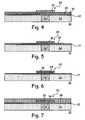
- FIG. 3is a cross sectional depiction of a first electrode according to a first preferred embodiment of a method according to the present invention.
- FIG. 4is a cross sectional depiction of a nanotube layer, metal layer, and dielectric layer overlaid with photoresist according to a first preferred embodiment of the method according to the present invention.
- FIG. 5is a cross sectional depiction of a patterned dielectric layer according to a first preferred embodiment of the method according to the present invention.
- FIG. 6is a cross sectional depiction of an etched metal layer that undercuts the dielectric layer according to a first preferred embodiment of the method according to the present invention.
- FIG. 7is a cross sectional depiction of a spacer metal layer according to a first preferred embodiment of the method according to the present invention.
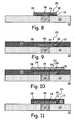
- FIG. 8is a cross sectional depiction of a patterned spacer metal layer according to a first preferred embodiment of the method according to the present invention.
- FIG. 9is a cross sectional depiction of a pad metal layer according to a first preferred embodiment of the method according to the present invention.
- FIG. 10is a cross sectional depiction of the pad metal layer patterned with photoresist according to a first preferred embodiment of the method according to the present invention.
- FIG. 11is a cross sectional depiction of the patterned pad metal layer according to a first preferred embodiment of the method according to the present invention.
- FIG. 12is a top plan depiction of a completed cell according to a first preferred embodiment of the method according to the present invention.
- FIG. 13is a cross sectional depiction of the completed cell according to a first preferred embodiment of the method according to the present invention.
- FIG. 14is a cross sectional depiction of a first electrode according to a second preferred embodiment of a method according to the present invention.
- FIG. 15is a cross sectional depiction of a nanotube layer, metal layer, and dielectric layer overlaid with photoresist according to a second preferred embodiment of the method according to the present invention.
- FIG. 16is a cross sectional depiction of a patterned nanotube layer, metal layer, and dielectric layer according to a second preferred embodiment of the method according to the present invention.
- FIG. 17is a cross sectional depiction of an etched back dielectric layer according to a second preferred embodiment of the method according to the present invention.
- FIG. 18is a cross sectional depiction of an etched metal layer that undercuts the dielectric layer according to a second preferred embodiment of the method according to the present invention.
- FIG. 19is a cross sectional depiction of a combination spacer and pad metal layer according to a second preferred embodiment of the method according to the present invention.
- FIG. 20is a cross sectional depiction of the combination spacer and pad metal layer patterned with photoresist according to a second preferred embodiment of the method according to the present invention.
- FIG. 21is a cross sectional depiction of the patterned combination spacer and pad metal layer according to a second preferred embodiment of the method according to the present invention.
- FIG. 22is a top plan depiction of a completed cell according to a second preferred embodiment of the method according to the present invention.
- FIG. 23is a cross sectional depiction of the completed cell according to a second preferred embodiment of the method according to the present invention.
- an interlayer dielectric layer 32is formed with a first or contact electrode 16 .
- the first electrodecan be formed of any conductive material, including one or more of doped polysilicon, contact metal such as W, or via material such as Al, Cu, TiN, and TaN.
- the nanotube layer 12is formed overlying the interlayer dielectric layer 32 , and a metal layer 34 is next formed, where the metal layer 34 can be one or more of any conductive material such as Co, TiN, and Al, and a dielectric layer 36 is then deposited, such as one or more of an oxide or a nitride.
- Photoresist 20is then applied and patterned.
- FIG. 5depicts the structure after the dielectric layer 36 has been etched, and the photoresist 24 has been stripped and cleaned.
- a non-plasma isotropic etch of metal layer 34is then performed, such as with a solution of NH 4 OH:H 2 O 2 :H 2 O.
- a spacer metal layer 38is then deposited, preferably formed of one or more materials such as TiN, Co, TaN, and Al, as depicted in FIG. 7 .
- the spacer metal layer 38 and the nanotube layer 12are then etched to produce the structure such as depicted in FIG. 8 .
- the etchis preferably performed such as with a wet chemical etch or an oxygen plasma. The plasma etch is acceptable at this point, because the remaining nanotube layer 12 is protected from the etch process.
- a pad metal layer 40is deposited, such as of at least one of Al and TiN, and optionally planarized, such as with a chemical mechanical planarization, as depicted in FIG. 9 .
- the pad metal layer 40is patterned with photoresist 24 as depicted in FIG. 10 , and etched and cleaned as depicted in FIG. 11 .
- the final cell structure 20is depicted from a top view in FIG. 12 and a cross-sectional view in FIG. 13 .
- the cell 20operates by applying a program voltage pulse between the bottom electrode 16 and the top electrode 40 , which causes the nanotube layer 12 to “heal” any voltage-induced cracks and become conductive between the bottom electrode 16 and the top electrode 40 , for an “on-state” condition.
- An erase voltage pulseis applied between the bottom electrode 16 and the top electrode 40 , which causes the nanotube layer 12 to sever and become nonconductive between the bottom electrode 16 and the top electrode 40 , for an “off-state” condition.
- the erase pulsecauses physical bond breaking of the nanotubes 12
- a program pulsecreates an electrostatic attraction between the severed ends of the nanotubes 12 , thereby bringing them back in contact.
- an interlayer dielectric layer 32is formed with a first or contact electrode 16 .
- the first electrodecan be formed of any conductive material, including one or more of doped polysilicon, contact metal such as W, or via material such as Al, Cu, TiN, and TaN.
- the nanotube layer 12is formed overlying the interlayer dielectric layer 32 , and a metal layer 34 is next formed, where the metal layer 34 can be any conductive material such as one or more of Co, TiN, and Al, and a dielectric layer 36 is then deposited, such as one or more of an oxide or a nitride.
- Photoresist 20is then applied and patterned.
- FIG. 16depicts the structure after the dielectric layer 36 , metal layer 34 , and the nanotube layer 12 have all been etched, and the photoresist 24 has been stripped and cleaned. As the nanotube layer 12 is protected by the overlying layers, this etch can be either a wet or plasma etch.
- the dielectric layer 36is then reduced such as with a wet isotropic etch of HF:H 2 O, as depicted in FIG. 17 .
- a non-plasma isotropic etchis then performed on the metal layer 34 , such as with a solution of NH 4 OH:H 2 O 2 :H 2 O, as depicted in FIG. 18 , so as to not expose the nanotube layer 12 to a plasma.
- a combination spacer metal layer and pad metal layer 40is then deposited as a single layer, formed of a material such as one or more of Al and TiN, as depicted in FIG. 19 .
- a post deposition planarizationsuch as a chemical mechanical planarization, is optionally performed.
- the combination spacer metal layer and pad metal layer 40is patterned with photoresist 24 as depicted in FIG. 20 , and etched and cleaned as depicted in FIG. 21 .
- the final cell structure 20is depicted from a top view in FIG. 22 and a cross-sectional view in FIG. 23 .
- the size of the cell 20 producedis scalable to any technology node, with the scaling dimensions of the cell 20 being proportional to the size of the underlying contact electrode.
- the formation of the sealed cavity 14separates the program electrode and the contact electrode without exposing the nanotube layer 12 to a plasma, which would be detrimental to it.
- the methodsprovide independent control of the spacing between the two electrodes and overlap of the nanotube layer 12 .
- the electrode spacingis independent of the alignment to the contact electrode.
- an inter-metallic dielectric layer wet etchcan be used to undercut the ends of the nanotube layer 12 after the metal spacer 34 etch, thereby creating a cavity, which is then enclosed during the pad metal 40 deposition.
- the spacer electrode 34can be selectively removed by wet or isotropic dry etch to limit the program electrode area to the pad electrode 40 .
- the pad electrode 40can be formed using a damascene scheme instead of the subtractive schemes described above.
Landscapes
- Engineering & Computer Science (AREA)
- Chemical & Material Sciences (AREA)
- Nanotechnology (AREA)
- Physics & Mathematics (AREA)
- Mathematical Physics (AREA)
- Theoretical Computer Science (AREA)
- Crystallography & Structural Chemistry (AREA)
- Manufacturing & Machinery (AREA)
- Semiconductor Memories (AREA)
Abstract
Description
- This application claims priority on provisional patent application 60/688,846, filed Jun. 8, 2005.
- This invention relates to the field of integrated circuit fabrication. More particularly, this invention relates to forming switching structures within integrated circuits.
- Carbon nanotube technology is quickly becoming a technological area that is making an impact on the field of microelectronic devices. As the term is used herein, “integrated circuit” includes devices such as those formed on monolithic semiconducting substrates, such as those formed of group IV materials like silicon or germanium, or group III-V compounds like gallium arsenide, or mixtures of such materials. The term includes all types of devices formed, such as memory and logic, and all designs of such devices, such as MOS and bipolar. The term also comprehends applications such as flat panel displays, solar cells, and charge coupled devices.
- Single-wall carbon nanotubes are quasi one-dimensional nanowires, which exhibit either metallic or semiconducting properties, depending upon their chirality and radius. Single-wall nanotubes have been demonstrated as both semiconducting layers in thin film transistors as well as metallic interconnects between metal layers.
- One technology uses carbon nanotubes as an electromechanical switch for non-volatile memory devices, where the nanotubes are spin-deposited over a patterned substrate surface. The
nanotubes 12 lay overtrenches 14 between afirst electrode 16 and asecond electrode 18 of anintegrated circuit 10, as depicted inFIG. 1 . Thedevice 20 is switched on by applying a bias to thesecond electrode 18, and switched off by removing the bias to thesecond electrode 18, and applying a bias to thefirst electrode 16. - A two-
terminal switching device 20 can be made by over-lapping a metal layer over ananotube layer 12, as depicted inFIG. 2 , where the metal layer is segmented into afirst electrode 16 and asecond electrode 18. - Current integration schemes for the two-
terminal cell 20 consist of patterning thenanotube layer 12 followed by alignment of the second orprogramming electrode 18 to overlap thenanotube layer 12 ends by a discrete distance, such as from about twenty-five nanometers to about seventy-five nanometers. The accuracy of the alignment is generally limited by the tolerances of the photolithography tool used, suggesting that electron beam or very short wavelength scanners are preferred to achieve the desired overlap. - What is needed, therefore, are alternate methods for the fabrication of nanotube structures that reduce the dependence of the process on critical alignment tools.
- The above and other needs are met by a method of forming a self-aligned logic cell by forming an electrically conductive bottom electrode. A carbon nanotube layer is formed over the bottom electrode with electrical continuity with the bottom electrode. An electrically conductive clamp layer is formed over the nanotube layer with electrical continuity with the nanotube layer. The clamp layer substantially completely covers the nanotube layer, thereby protecting the nanotube layer. An electrically nonconductive dielectric layer is formed over the clamp layer. The dielectric layer is etched with a first etchant that does not substantially etch the clamp layer. The clamp layer provides an etch stop to the first etchant and protects the nanotube layer from the first etchant. A remainder of the dielectric layer is left overlying the bottom electrode.
- The clamp layer is etched with an isotropic second etchant that does not substantially etch the dielectric layer and the nanotube layer, and which etches the clamp layer underneath a peripheral edge of the dielectric layer to a substantially uniform and desired degree, thereby creating an overlap of the dielectric layer, and causing a self-alignment between the clamp layer and the overlap of the dielectric layer. An electrically conductive spacer layer is formed over at least the nanotube layer that does not substantially underlie the dielectric layer, the spacer layer having electrical continuity with the nanotube layer. The spacer layer is etched to remove all of the spacer layer except a ring portion circumferentially disposed around the peripheral edge of the dielectric layer and overlying a portion of the nanotube layer. The nanotube layer is etched to remove all of the nanotube layer except those portions of the nanotube layer that are underlying at least one of the clamp layer, the dielectric layer, and the spacer layer, thereby causing a self-alignment between the clamp layer, the overlap to the dielectric layer, the spacer layer, and the nanotube layer.
- Because of the method in which the cell is formed, the critical elements of the cell, such as the spacing of the carbon nanotube layer between the electrically conductive electrodes, are self-aligned, thereby reducing alignment errors that might otherwise occur in the fabrication of the cell, that would tend to reduce cell performance and reliability.
- According to another aspect of the invention there is described a method of forming a self-aligned logic cell by forming an electrically conductive bottom electrode, and forming a carbon nanotube layer over the bottom electrode with electrical continuity with the bottom electrode. An electrically conductive clamp layer is formed over the nanotube layer with electrical continuity with the nanotube layer, where the clamp layer substantially completely covers the nanotube layer, thereby protecting the nanotube layer. An electrically nonconductive dielectric layer is formed over the clamp layer. The dielectric layer, the clamp layer, and the nanotube layer are etched with a first etchant to produce a stack of the dielectric layer, the clamp layer, and the nanotube layer remaining over the bottom electrode. Each of the dielectric layer, the clamp layer, and the nanotube layer have substantially equal size after the etch. The dielectric layer is etched with a second etchant that does not substantially etch the clamp layer and the nanotube layer, to reduce the size of the dielectric layer and leave a ring portion of the clamp layer exposed around a peripheral edge of the dielectric layer. The clamp layer is etched with an isotropic third etchant that does not substantially etch the dielectric layer and the nanotube layer, and which etches the clamp layer underneath the peripheral edge of the dielectric layer to a substantially uniform and desired degree, thereby creating an overlap of the dielectric layer, and causing a self-alignment between the clamp layer, the overlap of the dielectric layer, and the nanotube layer.
- Further advantages of the invention are apparent by reference to the detailed description when considered in conjunction with the figures, which are not to scale so as to more clearly show the details, wherein like reference numbers indicate like elements throughout the several views, and wherein:
FIG. 1 is a cross sectional depiction of a first prior art nanotube structure.FIG. 2 is a cross sectional depiction of a second prior art nanotube structure.FIG. 3 is a cross sectional depiction of a first electrode according to a first preferred embodiment of a method according to the present invention.FIG. 4 is a cross sectional depiction of a nanotube layer, metal layer, and dielectric layer overlaid with photoresist according to a first preferred embodiment of the method according to the present invention.FIG. 5 is a cross sectional depiction of a patterned dielectric layer according to a first preferred embodiment of the method according to the present invention.FIG. 6 is a cross sectional depiction of an etched metal layer that undercuts the dielectric layer according to a first preferred embodiment of the method according to the present invention.FIG. 7 is a cross sectional depiction of a spacer metal layer according to a first preferred embodiment of the method according to the present invention.FIG. 8 is a cross sectional depiction of a patterned spacer metal layer according to a first preferred embodiment of the method according to the present invention.FIG. 9 is a cross sectional depiction of a pad metal layer according to a first preferred embodiment of the method according to the present invention.FIG. 10 is a cross sectional depiction of the pad metal layer patterned with photoresist according to a first preferred embodiment of the method according to the present invention.FIG. 11 is a cross sectional depiction of the patterned pad metal layer according to a first preferred embodiment of the method according to the present invention.FIG. 12 is a top plan depiction of a completed cell according to a first preferred embodiment of the method according to the present invention.FIG. 13 is a cross sectional depiction of the completed cell according to a first preferred embodiment of the method according to the present invention.FIG. 14 is a cross sectional depiction of a first electrode according to a second preferred embodiment of a method according to the present invention.FIG. 15 is a cross sectional depiction of a nanotube layer, metal layer, and dielectric layer overlaid with photoresist according to a second preferred embodiment of the method according to the present invention.FIG. 16 is a cross sectional depiction of a patterned nanotube layer, metal layer, and dielectric layer according to a second preferred embodiment of the method according to the present invention.FIG. 17 is a cross sectional depiction of an etched back dielectric layer according to a second preferred embodiment of the method according to the present invention.FIG. 18 is a cross sectional depiction of an etched metal layer that undercuts the dielectric layer according to a second preferred embodiment of the method according to the present invention.FIG. 19 is a cross sectional depiction of a combination spacer and pad metal layer according to a second preferred embodiment of the method according to the present invention.FIG. 20 is a cross sectional depiction of the combination spacer and pad metal layer patterned with photoresist according to a second preferred embodiment of the method according to the present invention.FIG. 21 is a cross sectional depiction of the patterned combination spacer and pad metal layer according to a second preferred embodiment of the method according to the present invention.FIG. 22 is a top plan depiction of a completed cell according to a second preferred embodiment of the method according to the present invention.FIG. 23 is a cross sectional depiction of the completed cell according to a second preferred embodiment of the method according to the present invention.- By employing a self-aligned method as described herein, the effect of the tolerance of the photolithography tool is dramatically reduced and preferably eliminated. The following embodiments describe two examples of self-alignment methods that create the desired overlap.
- As depicted in
FIG. 3 , aninterlayer dielectric layer 32 is formed with a first orcontact electrode 16. The first electrode can be formed of any conductive material, including one or more of doped polysilicon, contact metal such as W, or via material such as Al, Cu, TiN, and TaN. - As depicted in
FIG. 4 , thenanotube layer 12 is formed overlying theinterlayer dielectric layer 32, and ametal layer 34 is next formed, where themetal layer 34 can be one or more of any conductive material such as Co, TiN, and Al, and adielectric layer 36 is then deposited, such as one or more of an oxide or a nitride.Photoresist 20 is then applied and patterned.FIG. 5 depicts the structure after thedielectric layer 36 has been etched, and thephotoresist 24 has been stripped and cleaned. - As depicted in
FIG. 6 , a non-plasma isotropic etch ofmetal layer 34 is then performed, such as with a solution of NH4OH:H2O2:H2O. As a plasma would tend to damage thenanotube layer 12, it is important that this etch step be performed without a plasma. Aspacer metal layer 38 is then deposited, preferably formed of one or more materials such as TiN, Co, TaN, and Al, as depicted inFIG. 7 . Thespacer metal layer 38 and thenanotube layer 12 are then etched to produce the structure such as depicted inFIG. 8 . The etch is preferably performed such as with a wet chemical etch or an oxygen plasma. The plasma etch is acceptable at this point, because the remainingnanotube layer 12 is protected from the etch process. - Next, a
pad metal layer 40 is deposited, such as of at least one of Al and TiN, and optionally planarized, such as with a chemical mechanical planarization, as depicted inFIG. 9 . Thepad metal layer 40 is patterned withphotoresist 24 as depicted inFIG. 10 , and etched and cleaned as depicted inFIG. 11 . Thefinal cell structure 20 is depicted from a top view inFIG. 12 and a cross-sectional view inFIG. 13 . - The
cell 20 operates by applying a program voltage pulse between thebottom electrode 16 and thetop electrode 40, which causes thenanotube layer 12 to “heal” any voltage-induced cracks and become conductive between thebottom electrode 16 and thetop electrode 40, for an “on-state” condition. An erase voltage pulse is applied between thebottom electrode 16 and thetop electrode 40, which causes thenanotube layer 12 to sever and become nonconductive between thebottom electrode 16 and thetop electrode 40, for an “off-state” condition. Thus, the erase pulse causes physical bond breaking of thenanotubes 12, while a program pulse creates an electrostatic attraction between the severed ends of thenanotubes 12, thereby bringing them back in contact. - As depicted in
FIG. 14 , aninterlayer dielectric layer 32 is formed with a first orcontact electrode 16. The first electrode can be formed of any conductive material, including one or more of doped polysilicon, contact metal such as W, or via material such as Al, Cu, TiN, and TaN. - As depicted in
FIG. 15 , thenanotube layer 12 is formed overlying theinterlayer dielectric layer 32, and ametal layer 34 is next formed, where themetal layer 34 can be any conductive material such as one or more of Co, TiN, and Al, and adielectric layer 36 is then deposited, such as one or more of an oxide or a nitride.Photoresist 20 is then applied and patterned.FIG. 16 depicts the structure after thedielectric layer 36,metal layer 34, and thenanotube layer 12 have all been etched, and thephotoresist 24 has been stripped and cleaned. As thenanotube layer 12 is protected by the overlying layers, this etch can be either a wet or plasma etch. - The
dielectric layer 36 is then reduced such as with a wet isotropic etch of HF:H2O, as depicted inFIG. 17 . A non-plasma isotropic etch is then performed on themetal layer 34, such as with a solution of NH4OH:H2O2:H2O, as depicted inFIG. 18 , so as to not expose thenanotube layer 12 to a plasma. - A combination spacer metal layer and
pad metal layer 40 is then deposited as a single layer, formed of a material such as one or more of Al and TiN, as depicted inFIG. 19 . A post deposition planarization, such as a chemical mechanical planarization, is optionally performed. The combination spacer metal layer andpad metal layer 40 is patterned withphotoresist 24 as depicted inFIG. 20 , and etched and cleaned as depicted inFIG. 21 . Thefinal cell structure 20 is depicted from a top view inFIG. 22 and a cross-sectional view inFIG. 23 . - These embodiments describe a self-aligned process that produces a small, controlled overlap of the program metal with the exposed ends of the
nanotube layer 12, and produces a self-passivatingnanotube layer 12. The size of thecell 20 produced is scalable to any technology node, with the scaling dimensions of thecell 20 being proportional to the size of the underlying contact electrode. The formation of the sealedcavity 14 separates the program electrode and the contact electrode without exposing thenanotube layer 12 to a plasma, which would be detrimental to it. The methods provide independent control of the spacing between the two electrodes and overlap of thenanotube layer 12. The electrode spacing is independent of the alignment to the contact electrode. These methods can be integrated to the process flow between any of the existing metal layers in the fabrication process of the integrated circuit. Further, the processes can be extended vertically to have multiple layers of the memory elements between each metal layer. Only two masking steps are required to build thecells 20. - In the first embodiment above, an inter-metallic dielectric layer wet etch can be used to undercut the ends of the
nanotube layer 12 after themetal spacer 34 etch, thereby creating a cavity, which is then enclosed during thepad metal 40 deposition. Also in embodiment one, thespacer electrode 34 can be selectively removed by wet or isotropic dry etch to limit the program electrode area to thepad electrode 40. In both of the two embodiments, thepad electrode 40 can be formed using a damascene scheme instead of the subtractive schemes described above. - The foregoing description of preferred embodiments for this invention has been presented for purposes of illustration and description. It is not intended to be exhaustive or to limit the invention to the precise form disclosed. Obvious modifications or variations are possible in light of the above teachings. The embodiments are chosen and described in an effort to provide the best illustrations of the principles of the invention and its practical application, and to thereby enable one of ordinary skill in the art to utilize the invention in various embodiments and with various modifications as are suited to the particular use contemplated. All such modifications and variations are within the scope of the invention as determined by the appended claims when interpreted in accordance with the breadth to which they are fairly, legally, and equitably entitled.
Claims (2)
Priority Applications (1)
| Application Number | Priority Date | Filing Date | Title |
|---|---|---|---|
| US11/312,849US7915122B2 (en) | 2005-06-08 | 2005-12-20 | Self-aligned cell integration scheme |
Applications Claiming Priority (2)
| Application Number | Priority Date | Filing Date | Title |
|---|---|---|---|
| US68884605P | 2005-06-08 | 2005-06-08 | |
| US11/312,849US7915122B2 (en) | 2005-06-08 | 2005-12-20 | Self-aligned cell integration scheme |
Publications (2)
| Publication Number | Publication Date |
|---|---|
| US20060281256A1true US20060281256A1 (en) | 2006-12-14 |
| US7915122B2 US7915122B2 (en) | 2011-03-29 |
Family
ID=37524588
Family Applications (1)
| Application Number | Title | Priority Date | Filing Date |
|---|---|---|---|
| US11/312,849Expired - Fee RelatedUS7915122B2 (en) | 2005-06-08 | 2005-12-20 | Self-aligned cell integration scheme |
Country Status (1)
| Country | Link |
|---|---|
| US (1) | US7915122B2 (en) |
Cited By (38)
| Publication number | Priority date | Publication date | Assignee | Title |
|---|---|---|---|---|
| US20060292716A1 (en)* | 2005-06-27 | 2006-12-28 | Lsi Logic Corporation | Use selective growth metallization to improve electrical connection between carbon nanotubes and electrodes |
| US20070121364A1 (en)* | 2003-06-09 | 2007-05-31 | Nantero, Inc. | One-time programmable, non-volatile field effect devices and methods of making same |
| US20070210845A1 (en)* | 2004-06-18 | 2007-09-13 | Nantero, Inc. | Storage elements using nanotube switching elements |
| US20080142850A1 (en)* | 2005-05-09 | 2008-06-19 | Nantero, Inc. | Memory elements and cross point switches and arrays of same using nonvolatile nanotube blocks |
| US7394687B2 (en) | 2005-05-09 | 2008-07-01 | Nantero, Inc. | Non-volatile-shadow latch using a nanotube switch |
| US20080158936A1 (en)* | 2005-05-09 | 2008-07-03 | Bertin Claude L | Nonvolatile resistive memories having scalable two-terminal nanotube switches |
| US20080159042A1 (en)* | 2005-05-09 | 2008-07-03 | Bertin Claude L | Latch circuits and operation circuits having scalable nonvolatile nanotube switches as electronic fuse replacement elements |
| US20080212361A1 (en)* | 2005-05-09 | 2008-09-04 | Nantero, Inc. | Nonvolatile nanotube diodes and nonvolatile nanotube blocks and systems using same and methods of making same |
| WO2008131836A1 (en)* | 2007-04-25 | 2008-11-06 | Merck Patent Gmbh | Process for preparing an electronic device |
| US20090194839A1 (en)* | 2005-11-15 | 2009-08-06 | Bertin Claude L | Nonvolatile nanotube diodes and nonvolatile nanotube blocks and systems using same and methods of making same |
| US20090211460A1 (en)* | 2007-11-20 | 2009-08-27 | Kwok Kuen So | Bowl and basket assembly and salad spinner incorporating such an assembly |
| US7598127B2 (en) | 2005-05-12 | 2009-10-06 | Nantero, Inc. | Nanotube fuse structure |
| US20090314530A1 (en)* | 2005-05-23 | 2009-12-24 | Nantero, Inc. | Method of aligning nanotubes and wires with an etched feature |
| US20100005645A1 (en)* | 2003-08-13 | 2010-01-14 | Bertin Claude L | Random access memory including nanotube switching elements |
| US20100038625A1 (en)* | 2008-08-14 | 2010-02-18 | Nantero, Inc. | Nonvolatile nanotube programmable logic devices and a nonvolatile nanotube field programmable gate array using same |
| US7781862B2 (en) | 2005-05-09 | 2010-08-24 | Nantero, Inc. | Two-terminal nanotube devices and systems and methods of making same |
| US20110051499A1 (en)* | 2009-08-12 | 2011-03-03 | Darlene Hamilton | Method for adjusting a resistive change element using a reference |
| US7915637B2 (en) | 2008-11-19 | 2011-03-29 | Nantero, Inc. | Switching materials comprising mixed nanoscopic particles and carbon nanotubes and method of making and using the same |
| US20110176359A1 (en)* | 2008-03-25 | 2011-07-21 | Nantero, Inc. | Carbon nanotube-based neural networks and methods of making and using same |
| US7986546B2 (en) | 2005-05-09 | 2011-07-26 | Nantero, Inc. | Non-volatile shadow latch using a nanotube switch |
| US8013363B2 (en) | 2005-05-09 | 2011-09-06 | Nantero, Inc. | Nonvolatile nanotube diodes and nonvolatile nanotube blocks and systems using same and methods of making same |
| US8110883B2 (en) | 2007-03-12 | 2012-02-07 | Nantero Inc. | Electromagnetic and thermal sensors using carbon nanotubes and methods of making same |
| US8128993B2 (en) | 2009-07-31 | 2012-03-06 | Nantero Inc. | Anisotropic nanotube fabric layers and films and methods of forming same |
| US8134220B2 (en) | 2007-06-22 | 2012-03-13 | Nantero Inc. | Two-terminal nanotube devices including a nanotube bridge and methods of making same |
| US8217490B2 (en) | 2005-05-09 | 2012-07-10 | Nantero Inc. | Nonvolatile nanotube diodes and nonvolatile nanotube blocks and systems using same and methods of making same |
| US8222704B2 (en) | 2009-12-31 | 2012-07-17 | Nantero, Inc. | Compact electrical switching devices with nanotube elements, and methods of making same |
| US8400053B2 (en) | 2001-07-25 | 2013-03-19 | Nantero Inc. | Carbon nanotube films, layers, fabrics, ribbons, elements and articles |
| US8513768B2 (en) | 2005-05-09 | 2013-08-20 | Nantero Inc. | Nonvolatile nanotube diodes and nonvolatile nanotube blocks and systems using same and methods of making same |
| US8574673B2 (en) | 2009-07-31 | 2013-11-05 | Nantero Inc. | Anisotropic nanotube fabric layers and films and methods of forming same |
| US8580586B2 (en) | 2005-05-09 | 2013-11-12 | Nantero Inc. | Memory arrays using nanotube articles with reprogrammable resistance |
| US9196615B2 (en) | 2005-05-09 | 2015-11-24 | Nantero Inc. | Nonvolatile nanotube diodes and nonvolatile nanotube blocks and systems using same and methods of making same |
| US9263126B1 (en) | 2010-09-01 | 2016-02-16 | Nantero Inc. | Method for dynamically accessing and programming resistive change element arrays |
| US9287356B2 (en) | 2005-05-09 | 2016-03-15 | Nantero Inc. | Nonvolatile nanotube diodes and nonvolatile nanotube blocks and systems using same and methods of making same |
| US9299430B1 (en) | 2015-01-22 | 2016-03-29 | Nantero Inc. | Methods for reading and programming 1-R resistive change element arrays |
| US9390790B2 (en) | 2005-04-05 | 2016-07-12 | Nantero Inc. | Carbon based nonvolatile cross point memory incorporating carbon based diode select devices and MOSFET select devices for memory and logic applications |
| US9911743B2 (en) | 2005-05-09 | 2018-03-06 | Nantero, Inc. | Nonvolatile nanotube diodes and nonvolatile nanotube blocks and systems using same and methods of making same |
| US9947400B2 (en) | 2016-04-22 | 2018-04-17 | Nantero, Inc. | Methods for enhanced state retention within a resistive change cell |
| US10355206B2 (en) | 2017-02-06 | 2019-07-16 | Nantero, Inc. | Sealed resistive change elements |
Families Citing this family (1)
| Publication number | Priority date | Publication date | Assignee | Title |
|---|---|---|---|---|
| US20100032640A1 (en)* | 2008-08-07 | 2010-02-11 | Sandisk 3D Llc | Memory cell that includes a carbon-based memory element and methods of forming the same |
Citations (85)
| Publication number | Priority date | Publication date | Assignee | Title |
|---|---|---|---|---|
| US4979149A (en)* | 1986-09-10 | 1990-12-18 | Lgz Landis & Gyr Zug Ag | Non-volatile memory device including a micro-mechanical storage element |
| US6057637A (en)* | 1996-09-13 | 2000-05-02 | The Regents Of The University Of California | Field emission electron source |
| US6100109A (en)* | 1994-11-02 | 2000-08-08 | Siemens Aktiengesellschaft | Method for producing a memory device |
| US6128214A (en)* | 1999-03-29 | 2000-10-03 | Hewlett-Packard | Molecular wire crossbar memory |
| US6187823B1 (en)* | 1998-10-02 | 2001-02-13 | University Of Kentucky Research Foundation | Solubilizing single-walled carbon nanotubes by direct reaction with amines and alkylaryl amines |
| US6250984B1 (en)* | 1999-01-25 | 2001-06-26 | Agere Systems Guardian Corp. | Article comprising enhanced nanotube emitter structure and process for fabricating article |
| US20010004979A1 (en)* | 1999-12-14 | 2001-06-28 | Lg Electronics Inc. | Field emission display and method for fabricating the same |
| US6256767B1 (en)* | 1999-03-29 | 2001-07-03 | Hewlett-Packard Company | Demultiplexer for a molecular wire crossbar network (MWCN DEMUX) |
| US6277318B1 (en)* | 1999-08-18 | 2001-08-21 | Agere Systems Guardian Corp. | Method for fabrication of patterned carbon nanotube films |
| US20010023986A1 (en)* | 2000-02-07 | 2001-09-27 | Vladimir Mancevski | System and method for fabricating logic devices comprising carbon nanotube transistors |
| US6314019B1 (en)* | 1999-03-29 | 2001-11-06 | Hewlett-Packard Company | Molecular-wire crossbar interconnect (MWCI) for signal routing and communications |
| US6331262B1 (en)* | 1998-10-02 | 2001-12-18 | University Of Kentucky Research Foundation | Method of solubilizing shortened single-walled carbon nanotubes in organic solutions |
| US6342276B1 (en)* | 1999-12-10 | 2002-01-29 | Samsung Sdi Co., Ltd. | Method for making a field emission display |
| US6368569B1 (en)* | 1998-10-02 | 2002-04-09 | University Of Kentucky Research Foundation | Method of solubilizing unshortened carbon nanotubes in organic solutions |
| US6409567B1 (en)* | 1997-12-15 | 2002-06-25 | E.I. Du Pont De Nemours And Company | Past-deposited carbon electron emitters |
| US20020081380A1 (en)* | 1999-08-12 | 2002-06-27 | Dillon Anne C. | Highly purified single-wall carbon nanotubes and production thereof |
| US6423583B1 (en)* | 2001-01-03 | 2002-07-23 | International Business Machines Corporation | Methodology for electrically induced selective breakdown of nanotubes |
| US6426687B1 (en)* | 2001-05-22 | 2002-07-30 | The Aerospace Corporation | RF MEMS switch |
| US6445006B1 (en)* | 1995-12-20 | 2002-09-03 | Advanced Technology Materials, Inc. | Microelectronic and microelectromechanical devices comprising carbon nanotube components, and methods of making same |
| US6443901B1 (en)* | 2000-06-15 | 2002-09-03 | Koninklijke Philips Electronics N.V. | Capacitive micromachined ultrasonic transducers |
| US20020160111A1 (en)* | 2001-04-25 | 2002-10-31 | Yi Sun | Method for fabrication of field emission devices using carbon nanotube film as a cathode |
| US20020175390A1 (en)* | 2001-04-03 | 2002-11-28 | Goldstein Seth Copen | Electronic circuit device, system, and method |
| US6495258B1 (en)* | 2000-09-20 | 2002-12-17 | Auburn University | Structures with high number density of carbon nanotubes and 3-dimensional distribution |
| US6495116B1 (en)* | 2000-04-10 | 2002-12-17 | Lockheed Martin Corporation | Net shape manufacturing using carbon nanotubes |
| US20030004058A1 (en)* | 2001-05-21 | 2003-01-02 | Trustees Of Boston College | Varied morphology carbon nanotubes and method for their manufacture |
| US6515339B2 (en)* | 2000-07-18 | 2003-02-04 | Lg Electronics Inc. | Method of horizontally growing carbon nanotubes and field effect transistor using the carbon nanotubes grown by the method |
| US6528020B1 (en)* | 1998-08-14 | 2003-03-04 | The Board Of Trustees Of The Leland Stanford Junior University | Carbon nanotube devices |
| US6548841B2 (en)* | 2000-11-09 | 2003-04-15 | Texas Instruments Incorporated | Nanomechanical switches and circuits |
| US20030122111A1 (en)* | 2001-03-26 | 2003-07-03 | Glatkowski Paul J. | Coatings comprising carbon nanotubes and methods for forming same |
| US20030177450A1 (en)* | 2002-03-12 | 2003-09-18 | Alex Nugent | Physical neural network design incorporating nanotechnology |
| US6630772B1 (en)* | 1998-09-21 | 2003-10-07 | Agere Systems Inc. | Device comprising carbon nanotube field emitter structure and process for forming device |
| US20030200521A1 (en)* | 2002-01-18 | 2003-10-23 | California Institute Of Technology | Array-based architecture for molecular electronics |
| US6645628B2 (en)* | 2001-11-13 | 2003-11-11 | The United States Of America As Represented By The Secretary Of The Air Force | Carbon nanotube coated anode |
| US20040007528A1 (en)* | 2002-07-03 | 2004-01-15 | The Regents Of The University Of California | Intertwined, free-standing carbon nanotube mesh for use as separation, concentration, and/or filtration medium |
| US20040023253A1 (en)* | 2001-06-11 | 2004-02-05 | Sandeep Kunwar | Device structure for closely spaced electrodes |
| US20040031975A1 (en)* | 2002-03-18 | 2004-02-19 | Max-Planck-Gesellschaft Zur Forderung Der Wissenschaften E.V., A German Corporation | Field effect transistor memory cell, memory device and method for manufacturing a field effect transistor memory cell |
| US20040043527A1 (en)* | 2002-09-04 | 2004-03-04 | Nanomix, Inc. | Sensitivity control for nanotube sensors |
| US20040041154A1 (en)* | 2002-09-04 | 2004-03-04 | Fuji Xerox Co., Ltd. | Electric part and method of manufacturing the same |
| US6707098B2 (en)* | 2000-07-04 | 2004-03-16 | Infineon Technologies, Ag | Electronic device and method for fabricating an electronic device |
| US20040057230A1 (en)* | 2002-09-21 | 2004-03-25 | Ching-Hui Lee | Innovated flashing decorative article |
| US20040071949A1 (en)* | 2001-07-27 | 2004-04-15 | Glatkowski Paul J. | Conformal coatings comprising carbon nanotubes |
| US20040099438A1 (en)* | 2002-05-21 | 2004-05-27 | Arthur David J. | Method for patterning carbon nanotube coating and carbon nanotube wiring |
| US20040104129A1 (en)* | 2002-11-27 | 2004-06-03 | Gang Gu | Nanotube chemical sensor based on work function of electrodes |
| US6759693B2 (en)* | 2002-06-19 | 2004-07-06 | Nantero, Inc. | Nanotube permeable base transistor |
| US6803840B2 (en)* | 2001-03-30 | 2004-10-12 | California Institute Of Technology | Pattern-aligned carbon nanotube growth and tunable resonator apparatus |
| US6809465B2 (en)* | 2002-08-23 | 2004-10-26 | Samsung Electronics Co., Ltd. | Article comprising MEMS-based two-dimensional e-beam sources and method for making the same |
| US6808746B1 (en)* | 1999-04-16 | 2004-10-26 | Commonwealth Scientific and Industrial Research Organisation Campell | Multilayer carbon nanotube films and method of making the same |
| US6809462B2 (en)* | 2000-04-05 | 2004-10-26 | Sri International | Electroactive polymer sensors |
| US20040238907A1 (en)* | 2003-06-02 | 2004-12-02 | Pinkerton Joseph F. | Nanoelectromechanical transistors and switch systems |
| US20040253167A1 (en)* | 2001-07-27 | 2004-12-16 | Silva Sembukutiarachilage Ravi | Production of carbon nanotubes |
| US6833558B2 (en)* | 2000-08-23 | 2004-12-21 | Korea Institute Of Science And Technology | Parallel and selective growth method of carbon nanotube on the substrates for electronic-spintronic device applications |
| US20040265550A1 (en)* | 2002-12-06 | 2004-12-30 | Glatkowski Paul J. | Optically transparent nanostructured electrical conductors |
| US6858197B1 (en)* | 2002-03-13 | 2005-02-22 | The United States Of America As Represented By The Administrator Of The National Aeronautics And Space Administration | Controlled patterning and growth of single wall and multi-wall carbon nanotubes |
| US6863942B2 (en)* | 1998-06-19 | 2005-03-08 | The Research Foundation Of State University Of New York | Free-standing and aligned carbon nanotubes and synthesis thereof |
| US20050053525A1 (en)* | 2003-05-14 | 2005-03-10 | Nantero, Inc. | Sensor platform using a horizontally oriented nanotube element |
| US20050056877A1 (en)* | 2003-03-28 | 2005-03-17 | Nantero, Inc. | Nanotube-on-gate fet structures and applications |
| US20050068128A1 (en)* | 2003-06-20 | 2005-03-31 | David Yip | Anchorless electrostatically activated micro electromechanical system switch |
| US20050083635A1 (en)* | 2003-10-17 | 2005-04-21 | Fuji Xerox Co., Ltd. | Capacitor and method of manufacturing the same |
| US20050095938A1 (en)* | 2003-10-29 | 2005-05-05 | Rosenberger Brian T. | Carbon nanotube fabrics |
| US6896864B2 (en)* | 2001-07-10 | 2005-05-24 | Battelle Memorial Institute | Spatial localization of dispersed single walled carbon nanotubes into useful structures |
| US6899945B2 (en)* | 2002-03-19 | 2005-05-31 | William Marsh Rice University | Entangled single-wall carbon nanotube solid material and methods for making same |
| US6919592B2 (en)* | 2001-07-25 | 2005-07-19 | Nantero, Inc. | Electromechanical memory array using nanotube ribbons and method for making same |
| US6918284B2 (en)* | 2003-03-24 | 2005-07-19 | The United States Of America As Represented By The Secretary Of The Navy | Interconnected networks of single-walled carbon nanotubes |
| US6919740B2 (en)* | 2003-01-31 | 2005-07-19 | Hewlett-Packard Development Company, Lp. | Molecular-junction-nanowire-crossbar-based inverter, latch, and flip-flop circuits, and more complex circuits composed, in part, from molecular-junction-nanowire-crossbar-based inverter, latch, and flip-flop circuits |
| US6921575B2 (en)* | 2001-05-21 | 2005-07-26 | Fuji Xerox Co., Ltd. | Carbon nanotube structures, carbon nanotube devices using the same and method for manufacturing carbon nanotube structures |
| US6924538B2 (en)* | 2001-07-25 | 2005-08-02 | Nantero, Inc. | Devices having vertically-disposed nanofabric articles and methods of making the same |
| US6946410B2 (en)* | 2002-04-05 | 2005-09-20 | E. I. Du Pont De Nemours And Company | Method for providing nano-structures of uniform length |
| US6955937B1 (en)* | 2004-08-12 | 2005-10-18 | Lsi Logic Corporation | Carbon nanotube memory cell for integrated circuit structure with removable side spacers to permit access to memory cell and process for forming such memory cell |
| US6969651B1 (en)* | 2004-03-26 | 2005-11-29 | Lsi Logic Corporation | Layout design and process to form nanotube cell for nanotube memory applications |
| US6990009B2 (en)* | 2003-08-13 | 2006-01-24 | Nantero, Inc. | Nanotube-based switching elements with multiple controls |
| US20060052509A1 (en)* | 2002-11-01 | 2006-03-09 | Mitsubishi Rayon Co., Ltd. | Composition containing carbon nanotubes having coating thereof and process for producing them |
| US7015500B2 (en)* | 2002-02-09 | 2006-03-21 | Samsung Electronics Co., Ltd. | Memory device utilizing carbon nanotubes |
| US7057402B2 (en)* | 2002-03-18 | 2006-06-06 | Honeywell International Inc. | Carbon nanotube sensor |
| US20060183278A1 (en)* | 2005-01-14 | 2006-08-17 | Nantero, Inc. | Field effect device having a channel of nanofabric and methods of making same |
| US20060204427A1 (en)* | 2004-12-16 | 2006-09-14 | Nantero, Inc. | Aqueous carbon nanotube applicator liquids and methods for producing applicator liquids thereof |
| US7115901B2 (en)* | 2003-06-09 | 2006-10-03 | Nantero, Inc. | Non-volatile electromechanical field effect devices and circuits using same and methods of forming same |
| US7115960B2 (en)* | 2003-08-13 | 2006-10-03 | Nantero, Inc. | Nanotube-based switching elements |
| US7115864B2 (en)* | 1996-08-08 | 2006-10-03 | William Marsh Rice University | Method for purification of as-produced single-wall carbon nanotubes |
| US20060237537A1 (en)* | 2002-09-30 | 2006-10-26 | Nanosys, Inc. | Applications of nano-enabled large area macroelectronic substrates incorporating nanowires and nanowire composites |
| US20060237799A1 (en)* | 2005-04-21 | 2006-10-26 | Lsi Logic Corporation | Carbon nanotube memory cells having flat bottom electrode contact surface |
| US20060258122A1 (en)* | 2005-05-12 | 2006-11-16 | Whitefield Bruce J | Nanotube fuse structure |
| US20060278902A1 (en)* | 2005-06-10 | 2006-12-14 | Sey-Shing Sun | Nano structure electrode design |
| US20070004191A1 (en)* | 2005-06-30 | 2007-01-04 | Lsi Logic Corporation | Novel techniques for precision pattern transfer of carbon nanotubes from photo mask to wafers |
| US20070003472A1 (en)* | 2003-03-24 | 2007-01-04 | Tolt Zhidan L | Electron emitting composite based on regulated nano-structures and a cold electron source using the composite |
| US7161403B2 (en)* | 2004-06-18 | 2007-01-09 | Nantero, Inc. | Storage elements using nanotube switching elements |
Family Cites Families (10)
| Publication number | Priority date | Publication date | Assignee | Title |
|---|---|---|---|---|
| EP1015384B1 (en) | 1997-03-07 | 2005-07-13 | William Marsh Rice University | Carbon fibers formed from single-wall carbon nanotubes |
| JP3943272B2 (en) | 1999-01-18 | 2007-07-11 | 双葉電子工業株式会社 | Film forming method of carbon nanotube |
| ES2264928T3 (en) | 1999-02-12 | 2007-02-01 | Board Of Trustees Operating Michigan State University | NANOCAPSULES CONTAINING LOADED PARTICLES, THEIR USES AND PROCEDURES FOR THE PREPARATION OF THE SAME. |
| EP2224508B1 (en) | 1999-07-02 | 2016-01-06 | President and Fellows of Harvard College | Method of separating metallic and semiconducting nanoscopic wires |
| JP4063451B2 (en) | 1999-07-26 | 2008-03-19 | 双葉電子工業株式会社 | Carbon nanotube pattern formation method |
| CA2430888C (en) | 2000-12-11 | 2013-10-22 | President And Fellows Of Harvard College | Nanosensors |
| US7566478B2 (en) | 2001-07-25 | 2009-07-28 | Nantero, Inc. | Methods of making carbon nanotube films, layers, fabrics, ribbons, elements and articles |
| KR100455284B1 (en) | 2001-08-14 | 2004-11-12 | 삼성전자주식회사 | High-throughput sensor for detecting biomolecules using carbon nanotubes |
| JP4306990B2 (en) | 2001-10-18 | 2009-08-05 | 独立行政法人産業技術総合研究所 | Nonlinear optical element |
| US6872645B2 (en) | 2002-04-02 | 2005-03-29 | Nanosys, Inc. | Methods of positioning and/or orienting nanostructures |
- 2005
- 2005-12-20USUS11/312,849patent/US7915122B2/ennot_activeExpired - Fee Related
Patent Citations (86)
| Publication number | Priority date | Publication date | Assignee | Title |
|---|---|---|---|---|
| US4979149A (en)* | 1986-09-10 | 1990-12-18 | Lgz Landis & Gyr Zug Ag | Non-volatile memory device including a micro-mechanical storage element |
| US6100109A (en)* | 1994-11-02 | 2000-08-08 | Siemens Aktiengesellschaft | Method for producing a memory device |
| US6445006B1 (en)* | 1995-12-20 | 2002-09-03 | Advanced Technology Materials, Inc. | Microelectronic and microelectromechanical devices comprising carbon nanotube components, and methods of making same |
| US7115864B2 (en)* | 1996-08-08 | 2006-10-03 | William Marsh Rice University | Method for purification of as-produced single-wall carbon nanotubes |
| US6057637A (en)* | 1996-09-13 | 2000-05-02 | The Regents Of The University Of California | Field emission electron source |
| US6409567B1 (en)* | 1997-12-15 | 2002-06-25 | E.I. Du Pont De Nemours And Company | Past-deposited carbon electron emitters |
| US6863942B2 (en)* | 1998-06-19 | 2005-03-08 | The Research Foundation Of State University Of New York | Free-standing and aligned carbon nanotubes and synthesis thereof |
| US6528020B1 (en)* | 1998-08-14 | 2003-03-04 | The Board Of Trustees Of The Leland Stanford Junior University | Carbon nanotube devices |
| US6630772B1 (en)* | 1998-09-21 | 2003-10-07 | Agere Systems Inc. | Device comprising carbon nanotube field emitter structure and process for forming device |
| US6187823B1 (en)* | 1998-10-02 | 2001-02-13 | University Of Kentucky Research Foundation | Solubilizing single-walled carbon nanotubes by direct reaction with amines and alkylaryl amines |
| US6331262B1 (en)* | 1998-10-02 | 2001-12-18 | University Of Kentucky Research Foundation | Method of solubilizing shortened single-walled carbon nanotubes in organic solutions |
| US6368569B1 (en)* | 1998-10-02 | 2002-04-09 | University Of Kentucky Research Foundation | Method of solubilizing unshortened carbon nanotubes in organic solutions |
| US6250984B1 (en)* | 1999-01-25 | 2001-06-26 | Agere Systems Guardian Corp. | Article comprising enhanced nanotube emitter structure and process for fabricating article |
| US6314019B1 (en)* | 1999-03-29 | 2001-11-06 | Hewlett-Packard Company | Molecular-wire crossbar interconnect (MWCI) for signal routing and communications |
| US6256767B1 (en)* | 1999-03-29 | 2001-07-03 | Hewlett-Packard Company | Demultiplexer for a molecular wire crossbar network (MWCN DEMUX) |
| US6128214A (en)* | 1999-03-29 | 2000-10-03 | Hewlett-Packard | Molecular wire crossbar memory |
| US6808746B1 (en)* | 1999-04-16 | 2004-10-26 | Commonwealth Scientific and Industrial Research Organisation Campell | Multilayer carbon nanotube films and method of making the same |
| US20020081380A1 (en)* | 1999-08-12 | 2002-06-27 | Dillon Anne C. | Highly purified single-wall carbon nanotubes and production thereof |
| US6277318B1 (en)* | 1999-08-18 | 2001-08-21 | Agere Systems Guardian Corp. | Method for fabrication of patterned carbon nanotube films |
| US6342276B1 (en)* | 1999-12-10 | 2002-01-29 | Samsung Sdi Co., Ltd. | Method for making a field emission display |
| US20010004979A1 (en)* | 1999-12-14 | 2001-06-28 | Lg Electronics Inc. | Field emission display and method for fabricating the same |
| US20010023986A1 (en)* | 2000-02-07 | 2001-09-27 | Vladimir Mancevski | System and method for fabricating logic devices comprising carbon nanotube transistors |
| US6809462B2 (en)* | 2000-04-05 | 2004-10-26 | Sri International | Electroactive polymer sensors |
| US6495116B1 (en)* | 2000-04-10 | 2002-12-17 | Lockheed Martin Corporation | Net shape manufacturing using carbon nanotubes |
| US6443901B1 (en)* | 2000-06-15 | 2002-09-03 | Koninklijke Philips Electronics N.V. | Capacitive micromachined ultrasonic transducers |
| US6707098B2 (en)* | 2000-07-04 | 2004-03-16 | Infineon Technologies, Ag | Electronic device and method for fabricating an electronic device |
| US6515339B2 (en)* | 2000-07-18 | 2003-02-04 | Lg Electronics Inc. | Method of horizontally growing carbon nanotubes and field effect transistor using the carbon nanotubes grown by the method |
| US6833558B2 (en)* | 2000-08-23 | 2004-12-21 | Korea Institute Of Science And Technology | Parallel and selective growth method of carbon nanotube on the substrates for electronic-spintronic device applications |
| US6495258B1 (en)* | 2000-09-20 | 2002-12-17 | Auburn University | Structures with high number density of carbon nanotubes and 3-dimensional distribution |
| US6548841B2 (en)* | 2000-11-09 | 2003-04-15 | Texas Instruments Incorporated | Nanomechanical switches and circuits |
| US6423583B1 (en)* | 2001-01-03 | 2002-07-23 | International Business Machines Corporation | Methodology for electrically induced selective breakdown of nanotubes |
| US20030122111A1 (en)* | 2001-03-26 | 2003-07-03 | Glatkowski Paul J. | Coatings comprising carbon nanotubes and methods for forming same |
| US6803840B2 (en)* | 2001-03-30 | 2004-10-12 | California Institute Of Technology | Pattern-aligned carbon nanotube growth and tunable resonator apparatus |
| US20020175390A1 (en)* | 2001-04-03 | 2002-11-28 | Goldstein Seth Copen | Electronic circuit device, system, and method |
| US20020160111A1 (en)* | 2001-04-25 | 2002-10-31 | Yi Sun | Method for fabrication of field emission devices using carbon nanotube film as a cathode |
| US6921575B2 (en)* | 2001-05-21 | 2005-07-26 | Fuji Xerox Co., Ltd. | Carbon nanotube structures, carbon nanotube devices using the same and method for manufacturing carbon nanotube structures |
| US20030004058A1 (en)* | 2001-05-21 | 2003-01-02 | Trustees Of Boston College | Varied morphology carbon nanotubes and method for their manufacture |
| US6426687B1 (en)* | 2001-05-22 | 2002-07-30 | The Aerospace Corporation | RF MEMS switch |
| US20040023253A1 (en)* | 2001-06-11 | 2004-02-05 | Sandeep Kunwar | Device structure for closely spaced electrodes |
| US6896864B2 (en)* | 2001-07-10 | 2005-05-24 | Battelle Memorial Institute | Spatial localization of dispersed single walled carbon nanotubes into useful structures |
| US6919592B2 (en)* | 2001-07-25 | 2005-07-19 | Nantero, Inc. | Electromechanical memory array using nanotube ribbons and method for making same |
| US6924538B2 (en)* | 2001-07-25 | 2005-08-02 | Nantero, Inc. | Devices having vertically-disposed nanofabric articles and methods of making the same |
| US20040253167A1 (en)* | 2001-07-27 | 2004-12-16 | Silva Sembukutiarachilage Ravi | Production of carbon nanotubes |
| US20040071949A1 (en)* | 2001-07-27 | 2004-04-15 | Glatkowski Paul J. | Conformal coatings comprising carbon nanotubes |
| US6645628B2 (en)* | 2001-11-13 | 2003-11-11 | The United States Of America As Represented By The Secretary Of The Air Force | Carbon nanotube coated anode |
| US20030200521A1 (en)* | 2002-01-18 | 2003-10-23 | California Institute Of Technology | Array-based architecture for molecular electronics |
| US7015500B2 (en)* | 2002-02-09 | 2006-03-21 | Samsung Electronics Co., Ltd. | Memory device utilizing carbon nanotubes |
| US20030177450A1 (en)* | 2002-03-12 | 2003-09-18 | Alex Nugent | Physical neural network design incorporating nanotechnology |
| US6858197B1 (en)* | 2002-03-13 | 2005-02-22 | The United States Of America As Represented By The Administrator Of The National Aeronautics And Space Administration | Controlled patterning and growth of single wall and multi-wall carbon nanotubes |
| US20040031975A1 (en)* | 2002-03-18 | 2004-02-19 | Max-Planck-Gesellschaft Zur Forderung Der Wissenschaften E.V., A German Corporation | Field effect transistor memory cell, memory device and method for manufacturing a field effect transistor memory cell |
| US7057402B2 (en)* | 2002-03-18 | 2006-06-06 | Honeywell International Inc. | Carbon nanotube sensor |
| US6899945B2 (en)* | 2002-03-19 | 2005-05-31 | William Marsh Rice University | Entangled single-wall carbon nanotube solid material and methods for making same |
| US6946410B2 (en)* | 2002-04-05 | 2005-09-20 | E. I. Du Pont De Nemours And Company | Method for providing nano-structures of uniform length |
| US20040099438A1 (en)* | 2002-05-21 | 2004-05-27 | Arthur David J. | Method for patterning carbon nanotube coating and carbon nanotube wiring |
| US6759693B2 (en)* | 2002-06-19 | 2004-07-06 | Nantero, Inc. | Nanotube permeable base transistor |
| US20040007528A1 (en)* | 2002-07-03 | 2004-01-15 | The Regents Of The University Of California | Intertwined, free-standing carbon nanotube mesh for use as separation, concentration, and/or filtration medium |
| US6809465B2 (en)* | 2002-08-23 | 2004-10-26 | Samsung Electronics Co., Ltd. | Article comprising MEMS-based two-dimensional e-beam sources and method for making the same |
| US20040041154A1 (en)* | 2002-09-04 | 2004-03-04 | Fuji Xerox Co., Ltd. | Electric part and method of manufacturing the same |
| US20040043527A1 (en)* | 2002-09-04 | 2004-03-04 | Nanomix, Inc. | Sensitivity control for nanotube sensors |
| US20040057230A1 (en)* | 2002-09-21 | 2004-03-25 | Ching-Hui Lee | Innovated flashing decorative article |
| US20060237537A1 (en)* | 2002-09-30 | 2006-10-26 | Nanosys, Inc. | Applications of nano-enabled large area macroelectronic substrates incorporating nanowires and nanowire composites |
| US20060052509A1 (en)* | 2002-11-01 | 2006-03-09 | Mitsubishi Rayon Co., Ltd. | Composition containing carbon nanotubes having coating thereof and process for producing them |
| US20040104129A1 (en)* | 2002-11-27 | 2004-06-03 | Gang Gu | Nanotube chemical sensor based on work function of electrodes |
| US20040265550A1 (en)* | 2002-12-06 | 2004-12-30 | Glatkowski Paul J. | Optically transparent nanostructured electrical conductors |
| US6919740B2 (en)* | 2003-01-31 | 2005-07-19 | Hewlett-Packard Development Company, Lp. | Molecular-junction-nanowire-crossbar-based inverter, latch, and flip-flop circuits, and more complex circuits composed, in part, from molecular-junction-nanowire-crossbar-based inverter, latch, and flip-flop circuits |
| US6918284B2 (en)* | 2003-03-24 | 2005-07-19 | The United States Of America As Represented By The Secretary Of The Navy | Interconnected networks of single-walled carbon nanotubes |
| US20070003472A1 (en)* | 2003-03-24 | 2007-01-04 | Tolt Zhidan L | Electron emitting composite based on regulated nano-structures and a cold electron source using the composite |
| US20050056877A1 (en)* | 2003-03-28 | 2005-03-17 | Nantero, Inc. | Nanotube-on-gate fet structures and applications |
| US20050053525A1 (en)* | 2003-05-14 | 2005-03-10 | Nantero, Inc. | Sensor platform using a horizontally oriented nanotube element |
| US20050065741A1 (en)* | 2003-05-14 | 2005-03-24 | Nantero, Inc. | Sensor platform using a non-horizontally oriented nanotube element |
| US20040238907A1 (en)* | 2003-06-02 | 2004-12-02 | Pinkerton Joseph F. | Nanoelectromechanical transistors and switch systems |
| US7115901B2 (en)* | 2003-06-09 | 2006-10-03 | Nantero, Inc. | Non-volatile electromechanical field effect devices and circuits using same and methods of forming same |
| US20050068128A1 (en)* | 2003-06-20 | 2005-03-31 | David Yip | Anchorless electrostatically activated micro electromechanical system switch |
| US6990009B2 (en)* | 2003-08-13 | 2006-01-24 | Nantero, Inc. | Nanotube-based switching elements with multiple controls |
| US7115960B2 (en)* | 2003-08-13 | 2006-10-03 | Nantero, Inc. | Nanotube-based switching elements |
| US20050083635A1 (en)* | 2003-10-17 | 2005-04-21 | Fuji Xerox Co., Ltd. | Capacitor and method of manufacturing the same |
| US20050095938A1 (en)* | 2003-10-29 | 2005-05-05 | Rosenberger Brian T. | Carbon nanotube fabrics |
| US6969651B1 (en)* | 2004-03-26 | 2005-11-29 | Lsi Logic Corporation | Layout design and process to form nanotube cell for nanotube memory applications |
| US7161403B2 (en)* | 2004-06-18 | 2007-01-09 | Nantero, Inc. | Storage elements using nanotube switching elements |
| US6955937B1 (en)* | 2004-08-12 | 2005-10-18 | Lsi Logic Corporation | Carbon nanotube memory cell for integrated circuit structure with removable side spacers to permit access to memory cell and process for forming such memory cell |
| US20060204427A1 (en)* | 2004-12-16 | 2006-09-14 | Nantero, Inc. | Aqueous carbon nanotube applicator liquids and methods for producing applicator liquids thereof |
| US20060183278A1 (en)* | 2005-01-14 | 2006-08-17 | Nantero, Inc. | Field effect device having a channel of nanofabric and methods of making same |
| US20060237799A1 (en)* | 2005-04-21 | 2006-10-26 | Lsi Logic Corporation | Carbon nanotube memory cells having flat bottom electrode contact surface |
| US20060258122A1 (en)* | 2005-05-12 | 2006-11-16 | Whitefield Bruce J | Nanotube fuse structure |
| US20060278902A1 (en)* | 2005-06-10 | 2006-12-14 | Sey-Shing Sun | Nano structure electrode design |
| US20070004191A1 (en)* | 2005-06-30 | 2007-01-04 | Lsi Logic Corporation | Novel techniques for precision pattern transfer of carbon nanotubes from photo mask to wafers |
Cited By (82)
| Publication number | Priority date | Publication date | Assignee | Title |
|---|---|---|---|---|
| US8400053B2 (en) | 2001-07-25 | 2013-03-19 | Nantero Inc. | Carbon nanotube films, layers, fabrics, ribbons, elements and articles |
| US20070121364A1 (en)* | 2003-06-09 | 2007-05-31 | Nantero, Inc. | One-time programmable, non-volatile field effect devices and methods of making same |
| US8125039B2 (en) | 2003-06-09 | 2012-02-28 | Nantero Inc. | One-time programmable, non-volatile field effect devices and methods of making same |
| US20100005645A1 (en)* | 2003-08-13 | 2010-01-14 | Bertin Claude L | Random access memory including nanotube switching elements |
| US7944735B2 (en) | 2003-08-13 | 2011-05-17 | Nantero, Inc. | Method of making a nanotube-based shadow random access memory |
| US20070210845A1 (en)* | 2004-06-18 | 2007-09-13 | Nantero, Inc. | Storage elements using nanotube switching elements |
| US7405605B2 (en) | 2004-06-18 | 2008-07-29 | Nantero, Inc. | Storage elements using nanotube switching elements |
| US7759996B2 (en) | 2004-06-18 | 2010-07-20 | Nantero, Inc. | Storage elements using nanotube switching elements |
| US9390790B2 (en) | 2005-04-05 | 2016-07-12 | Nantero Inc. | Carbon based nonvolatile cross point memory incorporating carbon based diode select devices and MOSFET select devices for memory and logic applications |
| US9783255B2 (en) | 2005-04-05 | 2017-10-10 | Nantero Inc. | Cross point arrays of 1-R nonvolatile resistive change memory cells using continuous nanotube fabrics |
| US9917139B2 (en) | 2005-04-05 | 2018-03-13 | Nantero Inc. | Resistive change element array using vertically oriented bit lines |
| US10339982B2 (en) | 2005-05-09 | 2019-07-02 | Nantero, Inc. | Memory elements and cross point switches and arrays of same using nonvolatile nanotube blocks |
| US8013363B2 (en) | 2005-05-09 | 2011-09-06 | Nantero, Inc. | Nonvolatile nanotube diodes and nonvolatile nanotube blocks and systems using same and methods of making same |
| US8217490B2 (en) | 2005-05-09 | 2012-07-10 | Nantero Inc. | Nonvolatile nanotube diodes and nonvolatile nanotube blocks and systems using same and methods of making same |
| US20080142850A1 (en)* | 2005-05-09 | 2008-06-19 | Nantero, Inc. | Memory elements and cross point switches and arrays of same using nonvolatile nanotube blocks |
| US8513768B2 (en) | 2005-05-09 | 2013-08-20 | Nantero Inc. | Nonvolatile nanotube diodes and nonvolatile nanotube blocks and systems using same and methods of making same |
| US7394687B2 (en) | 2005-05-09 | 2008-07-01 | Nantero, Inc. | Non-volatile-shadow latch using a nanotube switch |
| US9911743B2 (en) | 2005-05-09 | 2018-03-06 | Nantero, Inc. | Nonvolatile nanotube diodes and nonvolatile nanotube blocks and systems using same and methods of making same |
| US8102018B2 (en) | 2005-05-09 | 2012-01-24 | Nantero Inc. | Nonvolatile resistive memories having scalable two-terminal nanotube switches |
| US9767902B2 (en) | 2005-05-09 | 2017-09-19 | Nantero, Inc. | Non-volatile composite nanoscopic fabric NAND memory arrays and methods of making same |
| US8008745B2 (en) | 2005-05-09 | 2011-08-30 | Nantero, Inc. | Latch circuits and operation circuits having scalable nonvolatile nanotube switches as electronic fuse replacement elements |
| US9601498B2 (en) | 2005-05-09 | 2017-03-21 | Nantero Inc. | Two-terminal nanotube devices and systems and methods of making same |
| US20080212361A1 (en)* | 2005-05-09 | 2008-09-04 | Nantero, Inc. | Nonvolatile nanotube diodes and nonvolatile nanotube blocks and systems using same and methods of making same |
| US7781862B2 (en) | 2005-05-09 | 2010-08-24 | Nantero, Inc. | Two-terminal nanotube devices and systems and methods of making same |
| US7782650B2 (en) | 2005-05-09 | 2010-08-24 | Nantero, Inc. | Nonvolatile nanotube diodes and nonvolatile nanotube blocks and systems using same and methods of making same |
| US7835170B2 (en) | 2005-05-09 | 2010-11-16 | Nantero, Inc. | Memory elements and cross point switches and arrays of same using nonvolatile nanotube blocks |
| US9406349B2 (en) | 2005-05-09 | 2016-08-02 | Nantero Inc. | Memory elements and cross point switches and arrays for same using nonvolatile nanotube blocks |
| US20080159042A1 (en)* | 2005-05-09 | 2008-07-03 | Bertin Claude L | Latch circuits and operation circuits having scalable nonvolatile nanotube switches as electronic fuse replacement elements |
| US9287356B2 (en) | 2005-05-09 | 2016-03-15 | Nantero Inc. | Nonvolatile nanotube diodes and nonvolatile nanotube blocks and systems using same and methods of making same |
| US9196615B2 (en) | 2005-05-09 | 2015-11-24 | Nantero Inc. | Nonvolatile nanotube diodes and nonvolatile nanotube blocks and systems using same and methods of making same |
| US20080158936A1 (en)* | 2005-05-09 | 2008-07-03 | Bertin Claude L | Nonvolatile resistive memories having scalable two-terminal nanotube switches |
| US8809917B2 (en) | 2005-05-09 | 2014-08-19 | Nantero Inc. | Memory elements and cross point switches and arrays of same using nonvolatile nanotube blocks |
| US7986546B2 (en) | 2005-05-09 | 2011-07-26 | Nantero, Inc. | Non-volatile shadow latch using a nanotube switch |
| US8580586B2 (en) | 2005-05-09 | 2013-11-12 | Nantero Inc. | Memory arrays using nanotube articles with reprogrammable resistance |
| US7598127B2 (en) | 2005-05-12 | 2009-10-06 | Nantero, Inc. | Nanotube fuse structure |
| US8343373B2 (en) | 2005-05-23 | 2013-01-01 | Nantero Inc. | Method of aligning nanotubes and wires with an etched feature |
| US20090314530A1 (en)* | 2005-05-23 | 2009-12-24 | Nantero, Inc. | Method of aligning nanotubes and wires with an etched feature |
| US20060292716A1 (en)* | 2005-06-27 | 2006-12-28 | Lsi Logic Corporation | Use selective growth metallization to improve electrical connection between carbon nanotubes and electrodes |
| US20090194839A1 (en)* | 2005-11-15 | 2009-08-06 | Bertin Claude L | Nonvolatile nanotube diodes and nonvolatile nanotube blocks and systems using same and methods of making same |
| US8183665B2 (en) | 2005-11-15 | 2012-05-22 | Nantero Inc. | Nonvolatile nanotube diodes and nonvolatile nanotube blocks and systems using same and methods of making same |
| US8110883B2 (en) | 2007-03-12 | 2012-02-07 | Nantero Inc. | Electromagnetic and thermal sensors using carbon nanotubes and methods of making same |
| US8637343B2 (en) | 2007-04-25 | 2014-01-28 | Merck Patent Gmbh | Process for preparing an electronic device |
| US20100108999A1 (en)* | 2007-04-25 | 2010-05-06 | Merck Patent Gesellschaft Mit Beschrankter Hafting | Process for preparing an electronic device |
| WO2008131836A1 (en)* | 2007-04-25 | 2008-11-06 | Merck Patent Gmbh | Process for preparing an electronic device |
| GB2461670B (en)* | 2007-04-25 | 2012-05-16 | Merck Patent Gmbh | Process for preparing an electronic device |
| GB2461670A (en)* | 2007-04-25 | 2010-01-13 | Merck Patent Gmbh | Process for preparing an electronic device |
| US8134220B2 (en) | 2007-06-22 | 2012-03-13 | Nantero Inc. | Two-terminal nanotube devices including a nanotube bridge and methods of making same |
| US20090211460A1 (en)* | 2007-11-20 | 2009-08-27 | Kwok Kuen So | Bowl and basket assembly and salad spinner incorporating such an assembly |
| US8659940B2 (en) | 2008-03-25 | 2014-02-25 | Nantero Inc. | Carbon nanotube-based neural networks and methods of making and using same |
| US20110176359A1 (en)* | 2008-03-25 | 2011-07-21 | Nantero, Inc. | Carbon nanotube-based neural networks and methods of making and using same |
| US20100072459A1 (en)* | 2008-08-14 | 2010-03-25 | Nantero, Inc. | Nonvolatile nanotube programmable logic devices and a nonvolatile nanotube field programmable gate array using same |
| US8319205B2 (en) | 2008-08-14 | 2012-11-27 | Nantero Inc. | Nonvolatile nanotube programmable logic devices and a nonvolatile nanotube field programmable gate array using same |
| US8541843B2 (en) | 2008-08-14 | 2013-09-24 | Nantero Inc. | Nonvolatile nanotube programmable logic devices and a nonvolatile nanotube field programmable gate array using same |
| US20100134141A1 (en)* | 2008-08-14 | 2010-06-03 | Nantero, Inc. | Nonvolatile nanotube programmable logic devices and a nonvolatile nanotube field programmable gate array using same |
| US9412447B1 (en) | 2008-08-14 | 2016-08-09 | Nantero Inc. | DDR compatible memory circuit architecture for resistive change element arrays |
| US7847588B2 (en) | 2008-08-14 | 2010-12-07 | Nantero, Inc. | Nonvolatile nanotube programmable logic devices and a nonvolatile nanotube field programmable gate array using same |
| US20100038625A1 (en)* | 2008-08-14 | 2010-02-18 | Nantero, Inc. | Nonvolatile nanotube programmable logic devices and a nonvolatile nanotube field programmable gate array using same |
| US7852114B2 (en) | 2008-08-14 | 2010-12-14 | Nantero, Inc. | Nonvolatile nanotube programmable logic devices and a nonvolatile nanotube field programmable gate array using same |
| US8188763B2 (en) | 2008-08-14 | 2012-05-29 | Nantero, Inc. | Nonvolatile nanotube programmable logic devices and a nonvolatile nanotube field programmable gate array using same |
| US8357921B2 (en) | 2008-08-14 | 2013-01-22 | Nantero Inc. | Integrated three-dimensional semiconductor system comprising nonvolatile nanotube field effect transistors |
| US20100078723A1 (en)* | 2008-08-14 | 2010-04-01 | Nantero, Inc. | Nonvolatile nanotube programmable logic devices and a nonvolatile nanotube field programmable gate array using same |
| US9852793B2 (en) | 2008-08-14 | 2017-12-26 | Nantero, Inc. | Methods for programming and accessing DDR compatible resistive change element arrays |
| US20100039138A1 (en)* | 2008-08-14 | 2010-02-18 | Nantero, Inc. | Nonvolatile nanotube programmable logic devices and a nonvolatile nanotube field programmable gate array using same |
| US9337423B2 (en) | 2008-11-19 | 2016-05-10 | Nantero Inc. | Two-terminal switching device using a composite material of nanoscopic particles and carbon nanotubes |
| US7915637B2 (en) | 2008-11-19 | 2011-03-29 | Nantero, Inc. | Switching materials comprising mixed nanoscopic particles and carbon nanotubes and method of making and using the same |
| US8969142B2 (en) | 2008-11-19 | 2015-03-03 | Nantero Inc. | Switching materials comprising mixed nanoscopic particles and carbon nanotubes and methods of making and using the same |
| US20110183489A1 (en)* | 2008-11-19 | 2011-07-28 | Ghenciu Eliodor G | Switching materials comprising mixed nanoscopic particles and carbon nanotubes and method of making and using the same |
| US8586424B2 (en) | 2008-11-19 | 2013-11-19 | Nantero Inc. | Switching materials comprising mixed nanoscopic particles and carbon nanotubes and method of making and using the same |
| US10181569B2 (en) | 2008-11-19 | 2019-01-15 | Nantero, Inc. | Two-terminal switching devices comprising coated nanotube elements |
| US9755170B2 (en) | 2008-11-19 | 2017-09-05 | Nantero, Inc. | Resistive materials comprising mixed nanoscopic particles and carbon nanotubes |
| US8574673B2 (en) | 2009-07-31 | 2013-11-05 | Nantero Inc. | Anisotropic nanotube fabric layers and films and methods of forming same |
| US8128993B2 (en) | 2009-07-31 | 2012-03-06 | Nantero Inc. | Anisotropic nanotube fabric layers and films and methods of forming same |
| US9666272B2 (en) | 2009-08-06 | 2017-05-30 | Nantero Inc. | Resistive change element arrays using resistive reference elements |
| US20110051499A1 (en)* | 2009-08-12 | 2011-03-03 | Darlene Hamilton | Method for adjusting a resistive change element using a reference |
| US8619450B2 (en) | 2009-08-12 | 2013-12-31 | Nantero Inc. | Method for adjusting a resistive change element using a reference |
| US8000127B2 (en) | 2009-08-12 | 2011-08-16 | Nantero, Inc. | Method for resetting a resistive change memory element |
| US8222704B2 (en) | 2009-12-31 | 2012-07-17 | Nantero, Inc. | Compact electrical switching devices with nanotube elements, and methods of making same |
| US9263126B1 (en) | 2010-09-01 | 2016-02-16 | Nantero Inc. | Method for dynamically accessing and programming resistive change element arrays |
| US9715927B2 (en) | 2015-01-22 | 2017-07-25 | Nantero, Inc. | 1-R resistive change element arrays using resistive reference elements |
| US9299430B1 (en) | 2015-01-22 | 2016-03-29 | Nantero Inc. | Methods for reading and programming 1-R resistive change element arrays |
| US9947400B2 (en) | 2016-04-22 | 2018-04-17 | Nantero, Inc. | Methods for enhanced state retention within a resistive change cell |
| US10355206B2 (en) | 2017-02-06 | 2019-07-16 | Nantero, Inc. | Sealed resistive change elements |
Also Published As
| Publication number | Publication date |
|---|---|
| US7915122B2 (en) | 2011-03-29 |
Similar Documents
| Publication | Publication Date | Title |
|---|---|---|
| US7915122B2 (en) | Self-aligned cell integration scheme | |
| US9466794B2 (en) | Low form voltage resistive random access memory (RRAM) | |
| US9012307B2 (en) | Two terminal resistive switching device structure and method of fabricating | |
| US7413945B2 (en) | Electrically isolated pillars in active devices | |
| TWI566363B (en) | Semiconductor device and method of manufacturing the same | |
| US7687377B2 (en) | Method of fabricating phase change memory device | |
| US20140166961A1 (en) | Resistive random access memory (rram) and method of making | |
| US11856864B2 (en) | Sub 60nm etchless MRAM devices by ion beam etching fabricated T-shaped bottom electrode | |
| JP3513805B2 (en) | Field effect transistor having Mott transition channel layer and method of manufacturing the same | |
| CN102315224A (en) | Nonvolatile memory device using FinFET and manufacturing method thereof | |
| JP2743061B2 (en) | Structure in an integrated circuit including at least two conductive elements and method of manufacture thereof | |
| US20250317694A1 (en) | Top notch slit profile for mems device | |
| US6248508B1 (en) | Manufacturing a circuit element | |
| US10468593B1 (en) | Scaled nanotube electrode for low power multistage atomic switch | |
| US8345462B2 (en) | Resistive memory and method for manufacturing the same | |
| JP2000332133A (en) | Complementary field effect transistor structure and method of manufacturing the same | |
| CN100553004C (en) | Phase change memory and its manufacturing method | |
| US6773967B1 (en) | Method to prevent antifuse Si damage using sidewall spacers | |
| US11222844B2 (en) | Via structures for use in semiconductor devices | |
| CN111952301A (en) | integrated circuit | |
| US20170222049A1 (en) | Vertical transistor and the fabrication method | |
| US11818969B2 (en) | Memory devices and method of forming the same | |
| US7884430B2 (en) | Isolated metal plug process for use in fabricating carbon nanotube memory cells | |
| US9343666B2 (en) | Damascene metal-insulator-metal (MIM) device with improved scaleability | |
| JPH0823078A (en) | Manufacture of programmable element |
Legal Events
| Date | Code | Title | Description |
|---|---|---|---|
| AS | Assignment | Owner name:LSI LOGIC CORPORATION, CALIFORNIA Free format text:ASSIGNMENT OF ASSIGNORS INTEREST;ASSIGNORS:CARTER, RICHARD J.;BHATT, HEMANSHU D.;GU, SHIQUN;AND OTHERS;SIGNING DATES FROM 20051215 TO 20051219;REEL/FRAME:017397/0063 Owner name:LSI LOGIC CORPORATION, CALIFORNIA Free format text:ASSIGNMENT OF ASSIGNORS INTEREST;ASSIGNORS:CARTER, RICHARD J.;BHATT, HEMANSHU D.;GU, SHIQUN;AND OTHERS;REEL/FRAME:017397/0063;SIGNING DATES FROM 20051215 TO 20051219 | |
| AS | Assignment | Owner name:LSI CORPORATION, CALIFORNIA Free format text:MERGER;ASSIGNOR:LSI SUBSIDIARY CORP.;REEL/FRAME:020548/0977 Effective date:20070404 Owner name:LSI CORPORATION,CALIFORNIA Free format text:MERGER;ASSIGNOR:LSI SUBSIDIARY CORP.;REEL/FRAME:020548/0977 Effective date:20070404 | |
| AS | Assignment | Owner name:NANTERO, INC., MASSACHUSETTS Free format text:ASSIGNMENT OF ASSIGNORS INTEREST;ASSIGNOR:LSI LOGIC CORPORATION;REEL/FRAME:020930/0839 Effective date:20080422 Owner name:NANTERO, INC.,MASSACHUSETTS Free format text:ASSIGNMENT OF ASSIGNORS INTEREST;ASSIGNOR:LSI LOGIC CORPORATION;REEL/FRAME:020930/0839 Effective date:20080422 | |
| AS | Assignment | Owner name:LOCKHEED MARTIN CORPORATION, MARYLAND Free format text:LICENSE;ASSIGNOR:NANTERO, INC.;REEL/FRAME:021411/0337 Effective date:20080813 Owner name:LOCKHEED MARTIN CORPORATION,MARYLAND Free format text:LICENSE;ASSIGNOR:NANTERO, INC.;REEL/FRAME:021411/0337 Effective date:20080813 | |
| AS | Assignment | Owner name:NANTERO, INC., MASSACHUSETTS Free format text:ASSIGNMENT OF ASSIGNORS INTEREST;ASSIGNOR:LSI CORPORATION;REEL/FRAME:021450/0389 Effective date:20080429 Owner name:NANTERO, INC.,MASSACHUSETTS Free format text:ASSIGNMENT OF ASSIGNORS INTEREST;ASSIGNOR:LSI CORPORATION;REEL/FRAME:021450/0389 Effective date:20080429 | |
| REMI | Maintenance fee reminder mailed | ||
| LAPS | Lapse for failure to pay maintenance fees | ||
| STCH | Information on status: patent discontinuation | Free format text:PATENT EXPIRED DUE TO NONPAYMENT OF MAINTENANCE FEES UNDER 37 CFR 1.362 | |
| FP | Lapsed due to failure to pay maintenance fee | Effective date:20150329 | |
| AS | Assignment | Owner name:ZEON CORPORATION, JAPAN Free format text:ASSIGNMENT OF ASSIGNORS INTEREST;ASSIGNOR:NANTERO, INC.;REEL/FRAME:056789/0932 Effective date:20210706 |