US20060279684A1 - Fringe field switching mode LCD - Google Patents
Fringe field switching mode LCDDownload PDFInfo
- Publication number
- US20060279684A1 US20060279684A1US11/215,235US21523505AUS2006279684A1US 20060279684 A1US20060279684 A1US 20060279684A1US 21523505 AUS21523505 AUS 21523505AUS 2006279684 A1US2006279684 A1US 2006279684A1
- Authority
- US
- United States
- Prior art keywords
- pixel electrodes
- mode lcd
- pixel
- liquid crystal
- electric field
- Prior art date
- Legal status (The legal status is an assumption and is not a legal conclusion. Google has not performed a legal analysis and makes no representation as to the accuracy of the status listed.)
- Granted
Links
- 239000004973liquid crystal related substanceSubstances0.000claimsabstractdescription34
- 239000000758substrateSubstances0.000claimsabstractdescription18
- 239000012212insulatorSubstances0.000claimsabstractdescription9
- 230000005684electric fieldEffects0.000claimsdescription33
- 239000002131composite materialSubstances0.000claimsdescription11
- 239000010410layerSubstances0.000claimsdescription9
- 239000011241protective layerSubstances0.000claimsdescription3
- 230000000630rising effectEffects0.000description7
- 239000011521glassSubstances0.000description6
- 238000002834transmittanceMethods0.000description5
- 238000007792additionMethods0.000description1
- 238000013459approachMethods0.000description1
- 239000004020conductorSubstances0.000description1
- 238000012986modificationMethods0.000description1
- 230000004048modificationEffects0.000description1
- 238000006467substitution reactionMethods0.000description1
Images


Classifications
- G—PHYSICS
- G02—OPTICS
- G02F—OPTICAL DEVICES OR ARRANGEMENTS FOR THE CONTROL OF LIGHT BY MODIFICATION OF THE OPTICAL PROPERTIES OF THE MEDIA OF THE ELEMENTS INVOLVED THEREIN; NON-LINEAR OPTICS; FREQUENCY-CHANGING OF LIGHT; OPTICAL LOGIC ELEMENTS; OPTICAL ANALOGUE/DIGITAL CONVERTERS
- G02F1/00—Devices or arrangements for the control of the intensity, colour, phase, polarisation or direction of light arriving from an independent light source, e.g. switching, gating or modulating; Non-linear optics
- G02F1/01—Devices or arrangements for the control of the intensity, colour, phase, polarisation or direction of light arriving from an independent light source, e.g. switching, gating or modulating; Non-linear optics for the control of the intensity, phase, polarisation or colour
- G02F1/13—Devices or arrangements for the control of the intensity, colour, phase, polarisation or direction of light arriving from an independent light source, e.g. switching, gating or modulating; Non-linear optics for the control of the intensity, phase, polarisation or colour based on liquid crystals, e.g. single liquid crystal display cells
- G02F1/133—Constructional arrangements; Operation of liquid crystal cells; Circuit arrangements
- G02F1/1333—Constructional arrangements; Manufacturing methods
- G02F1/1343—Electrodes
- G02F1/134309—Electrodes characterised by their geometrical arrangement
- G—PHYSICS
- G02—OPTICS
- G02F—OPTICAL DEVICES OR ARRANGEMENTS FOR THE CONTROL OF LIGHT BY MODIFICATION OF THE OPTICAL PROPERTIES OF THE MEDIA OF THE ELEMENTS INVOLVED THEREIN; NON-LINEAR OPTICS; FREQUENCY-CHANGING OF LIGHT; OPTICAL LOGIC ELEMENTS; OPTICAL ANALOGUE/DIGITAL CONVERTERS
- G02F1/00—Devices or arrangements for the control of the intensity, colour, phase, polarisation or direction of light arriving from an independent light source, e.g. switching, gating or modulating; Non-linear optics
- G02F1/01—Devices or arrangements for the control of the intensity, colour, phase, polarisation or direction of light arriving from an independent light source, e.g. switching, gating or modulating; Non-linear optics for the control of the intensity, phase, polarisation or colour
- G02F1/13—Devices or arrangements for the control of the intensity, colour, phase, polarisation or direction of light arriving from an independent light source, e.g. switching, gating or modulating; Non-linear optics for the control of the intensity, phase, polarisation or colour based on liquid crystals, e.g. single liquid crystal display cells
- G02F1/133—Constructional arrangements; Operation of liquid crystal cells; Circuit arrangements
- G02F1/1333—Constructional arrangements; Manufacturing methods
- G02F1/1343—Electrodes
- G02F1/134309—Electrodes characterised by their geometrical arrangement
- G02F1/134372—Electrodes characterised by their geometrical arrangement for fringe field switching [FFS] where the common electrode is not patterned
Definitions
- the present inventionrelates to a fringe field switching mode LCD, and more particularly to a fringe field switching mode LCD adapted to adjust the angle between the liquid crystal director and the composite electric field in the fringe field switching mode to improve the gray-to-gray response time.
- FFS-mode LCDhas been proposed to improve the low aperture ratio and transmittance of in-plane switching mode (hereinafter, referred to as IPS-mode) LCDs, as disclosed in Korean Registered Patent No. 10-0341123.
- FIG. 1shows a conventional FFS-mode LCD.
- the FFS-mode LCD 10includes a lower glass substrate 11 ; a counter electrode 12 and a pixel electrode 13 formed on the lower glass substrate 10 using ITO with a gate insulator 14 interposed between them; an upper glass substrate 15 ; and a color filter 16 formed on the upper glass substrate 15 with a liquid crystal layer 17 interposed between them, which is composed of a number of liquid crystal molecules.
- the lower and upper glass substrates 11 and 15are bonded to each other.
- the FFS-mode LCD 10 constructed as abovehas higher aperture ratio and transmittance than IPS-mode LCDs, because the counter electrode 12 and the pixel electrode 13 are made of a transparent conductor.
- the spacing between the counter electrode 12 and the pixel electrode 13is smaller than that between the upper and lower glass substrates 11 and 15 to establish a fringe field between the counter electrode 12 and the pixel electrode 13 .
- even the liquid crystal molecules existing on top of the electrode 13are operated and improve the transmittance.
- the transmittance control in the FFS-mode LCDis performed by controlling the twist angle of liquid crystals.
- the liquid crystalsare rubbed while director being about 83° relative to the electric field direction, as shown in FIG. 2 .
- Equation 1the dielectric torque N in the denominator determines the rising response time and the remaining values are constants.
- ⁇ E 0 2 sin 2 ⁇ (Equation 2)
- FIG. 3shows the angle between the electric field and the average director of the liquid crystal molecules corresponding to each gray level, when the gray level varies in the FFS-mode LCD. It is clear from FIG. 3 that, as the gray level increases and the angle approaches 45°, the rising gray-to-gray response time becomes faster and, as the angle goes beneath 45° and becomes smaller, the rising gray-to-tray response time becomes slower again.
- an object of the present inventionis to provide a fringe field switching mode LCD capable of maintaining the fastest response time regardless of varying gray level.
- a fringe field switching mode LCDincluding a lower substrate having a gate bus line and a data bus line arranged to cross each other and form unit pixels and a counter electrode and a pixel electrode positioned within each unit pixel region with a gate insulator interposed between them and an upper substrate provided with a color filter corresponding to each pixel region and bonded to the lower substrate with a liquid crystal layer interposed between them, wherein the pixel electrode includes first pixel electrodes positioned on the gate insulator while being spaced from each other and second pixel electrodes positioned between the respective first pixel electrodes with a predetermined angle relative to them.
- the first pixel electrodesare preferably positioned on top of the second pixel electrodes while being electrically connected thereto with a protective layer being interposed between them.
- the predetermined angleis equal to the angle between the electric field caused by the first pixel electrodes and that caused by the second pixel electrodes and is in the range of 30-60°.
- the direction of the composite electric field of the electric field caused by the first pixel electrodes and that caused by the second pixel electrodespreferably maintains a predetermined angle relative to the direction of the liquid crystal molecules of the liquid crystal layer.
- the angle between the composite electric field and the liquid crystal directoris preferably in the range of 30-60°.
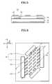
- FIG. 1is a sectional view showing a conventional FFS-mode LCD
- FIG. 2is a top view showing the pixel electrode and the initial liquid crystal molecules' direction of the FFS-mode LCD shown in FIG. 1 ;
- FIG. 3shows the change of angle between the liquid crystal director and the electric field as the gray level varies in the FFS-mode LCD shown in FIG. 1 ;
- FIG. 4is a top view showing an FFS-mode LCD according to an embodiment of the present invention.
- FIG. 5is a sectional view taken along line V-V′ of the FFS-mode LCD shown in FIG. 4 ;
- FIG. 6is a top view showing the pixel electrode and the initial liquid crystal molecules' direction of the FFS-mode LCD shown in FIG. 4 ;
- FIG. 7shows the change of angle between the liquid crystal director and the electric field as the gray level varies in the FFS-mode LCD shown in FIG. 7 .
- FIG. 4is a top view showing an FFS-mode LCD according to an embodiment of the present invention and FIG. 5 is a sectional view taken along line V-V′ of the FFS-mode LCD shown in FIG. 4 .
- the FFS-mode LCD 100includes a lower substrate (not shown) having a gate bus line 112 and a data bus line 111 arranged to cross each other and form unit pixels, as well as a counter electrode 120 and a pixel electrode 130 positioned in each unit pixel region with a gate insulator 140 interposed between them and an upper substrate (not shown) having a color filter (not shown) corresponding to each pixel region and bonded to the lower substrate with a liquid crystal layer (not shown) interposed between them.
- the components not shown in the drawingscan be easily understood by those skilled in the art and detailed description thereof will be omitted.
- the pixel electrode 130includes first pixel electrodes 131 positioned on the gate insulator 140 while being spaced from each other and second pixel electrodes 132 positioned between the respective first pixel electrodes 131 with a predetermined angle relative to them.
- the first and second pixel electrodes 131 and 132may be positioned on the same layer or on different layers with a protective layer 150 interposed between them.
- the first and second pixel electrodes 131 and 132are electrically connected to each other via contact holes 141 and 142 .
- the liquid crystal director 160 of the liquid crystal layerare aligned with an angle of 45° relative to the electric field from the first pixel electrode 131 .
- the angle between the first and second pixel electrodes 131 and 132is equal to the angle between the electric field direction of the first pixel electrodes 131 and that of the second pixel electrodes 132 and is in the range of 30-60°. The most preferable angle in this range is 45°.
- Such an angular rangeis aimed to obtain an angle of 30-60°, preferably 45°, between the composite electric field, which combines the electric field of the first pixel electrodes 131 with that of the second pixel electrodes 132 , and the liquid crystal director 160 .
- the angle between electric field direction of the second pixel electrodes 132 and the liquid crystal director 160is about 90°.
- the angle between the electric field direction of the first pixel electrodes 131 and the alignment direction of the liquid crystal molecules 160is 30-60°, preferably 45°, and the angle between the second pixel electrodes 132 and the electric field of the first pixel electrodes 131 is 30-60°, in order to improve the rising gray-to-gray response time.
- the liquid crystal molecules' directionmaintains an angle of 45° relative to the initial composite electric field direction, even when the gray level varies. Therefore, the angle between the initially-applied composite electric field and the liquid crystal director is always 45° at all gray levels.
- the liquid crystal moleculesrotate in the clockwise direction as the gray level increases and the electric field must be rotated in the same direction to maintain the direction of the initial electric field at 45°.
- the electric field intensity of the first and second pixel electrodesis separately varied so that the direction of the initial composite electric field maintains an angle of 45° relative to the liquid crystal director at all gray levels.
- the vector sumi.e., composite electric field
- the vector sum of the electric field of the first pixel electrodes 131 and that of the second pixel electrodes 132maintains a constant angle relative to the initial liquid crystal director at all gray levels and improves the response time.
- the FFS-mode LCD according to the present inventionis advantageous in that the second pixel electrodes are positioned with a predetermined angle relative to the first pixel electrodes so that the composite electric field of the first pixel electrodes' electric field and the second pixel electrodes' electric field and the alignment direction of the liquid crystal molecules maintain the optimum state, regardless of the varying gray level, to improve the rising gray-to-gray response time.
Landscapes
- Physics & Mathematics (AREA)
- Nonlinear Science (AREA)
- Mathematical Physics (AREA)
- Chemical & Material Sciences (AREA)
- Crystallography & Structural Chemistry (AREA)
- General Physics & Mathematics (AREA)
- Optics & Photonics (AREA)
- Liquid Crystal (AREA)
- Geometry (AREA)
Abstract
Description
- 1. Field of the invention
- The present invention relates to a fringe field switching mode LCD, and more particularly to a fringe field switching mode LCD adapted to adjust the angle between the liquid crystal director and the composite electric field in the fringe field switching mode to improve the gray-to-gray response time.
- 2. Description of the Prior Art
- A fringe field switching mode (hereinafter, referred to as FFS-mode) LCD has been proposed to improve the low aperture ratio and transmittance of in-plane switching mode (hereinafter, referred to as IPS-mode) LCDs, as disclosed in Korean Registered Patent No. 10-0341123.
FIG. 1 shows a conventional FFS-mode LCD.- Referring to the drawing, the FFS-
mode LCD 10 includes alower glass substrate 11; acounter electrode 12 and apixel electrode 13 formed on thelower glass substrate 10 using ITO with agate insulator 14 interposed between them; anupper glass substrate 15; and acolor filter 16 formed on theupper glass substrate 15 with aliquid crystal layer 17 interposed between them, which is composed of a number of liquid crystal molecules. The lower andupper glass substrates - The FFS-
mode LCD 10 constructed as above has higher aperture ratio and transmittance than IPS-mode LCDs, because thecounter electrode 12 and thepixel electrode 13 are made of a transparent conductor. In addition, the spacing between thecounter electrode 12 and thepixel electrode 13 is smaller than that between the upper andlower glass substrates counter electrode 12 and thepixel electrode 13. As a result, even the liquid crystal molecules existing on top of theelectrode 13 are operated and improve the transmittance. - The transmittance control in the FFS-mode LCD is performed by controlling the twist angle of liquid crystals. For a high transmittance, the liquid crystals are rubbed while director being about 83° relative to the electric field direction, as shown in
FIG. 2 . - The rising response time of the liquid crystals is determined by the following equation:
τon=r1/{N−(π2/d2)/K2 (Equation 1) - In
Equation 1, the dielectric torque N in the denominator determines the rising response time and the remaining values are constants. The dielectric torque N is expressed as follows:
N=|Δε(n·E)n×E|=ΔεE02sin 2Ψ (Equation 2) - It is clear from both equations that, under the condition of the same electric field intensity, the fastest rising response time is obtained when sin 2Ψ=1(Ψ=45°), particularly, when the angle between the alignment direction of the liquid crystal molecules and the direction of the initial electric field is 45°.
FIG. 3 shows the angle between the electric field and the average director of the liquid crystal molecules corresponding to each gray level, when the gray level varies in the FFS-mode LCD. It is clear fromFIG. 3 that, as the gray level increases and the angle approaches 45°, the rising gray-to-gray response time becomes faster and, as the angle goes beneath 45° and becomes smaller, the rising gray-to-tray response time becomes slower again.- Accordingly, the present invention has been made to solve the above-mentioned problems occurring in the prior art, and an object of the present invention is to provide a fringe field switching mode LCD capable of maintaining the fastest response time regardless of varying gray level.
- In order to accomplish this object, there is provided a fringe field switching mode LCD including a lower substrate having a gate bus line and a data bus line arranged to cross each other and form unit pixels and a counter electrode and a pixel electrode positioned within each unit pixel region with a gate insulator interposed between them and an upper substrate provided with a color filter corresponding to each pixel region and bonded to the lower substrate with a liquid crystal layer interposed between them, wherein the pixel electrode includes first pixel electrodes positioned on the gate insulator while being spaced from each other and second pixel electrodes positioned between the respective first pixel electrodes with a predetermined angle relative to them.
- The first pixel electrodes are preferably positioned on top of the second pixel electrodes while being electrically connected thereto with a protective layer being interposed between them.
- Preferably, the predetermined angle is equal to the angle between the electric field caused by the first pixel electrodes and that caused by the second pixel electrodes and is in the range of 30-60°.
- The direction of the composite electric field of the electric field caused by the first pixel electrodes and that caused by the second pixel electrodes preferably maintains a predetermined angle relative to the direction of the liquid crystal molecules of the liquid crystal layer.
- The angle between the composite electric field and the liquid crystal director is preferably in the range of 30-60°.
- The above and other objects, features and advantages of the present invention will be more apparent from the following detailed description taken in conjunction with the accompanying drawings, in which:
FIG. 1 is a sectional view showing a conventional FFS-mode LCD;FIG. 2 is a top view showing the pixel electrode and the initial liquid crystal molecules' direction of the FFS-mode LCD shown inFIG. 1 ;FIG. 3 shows the change of angle between the liquid crystal director and the electric field as the gray level varies in the FFS-mode LCD shown inFIG. 1 ;FIG. 4 is a top view showing an FFS-mode LCD according to an embodiment of the present invention;FIG. 5 is a sectional view taken along line V-V′ of the FFS-mode LCD shown inFIG. 4 ;FIG. 6 is a top view showing the pixel electrode and the initial liquid crystal molecules' direction of the FFS-mode LCD shown inFIG. 4 ; andFIG. 7 shows the change of angle between the liquid crystal director and the electric field as the gray level varies in the FFS-mode LCD shown inFIG. 7 .- Hereinafter, a preferred embodiment of the present invention will be described with reference to the accompanying drawings. In the following description and drawings, the same reference numerals are used to designate the same or similar components, and so repetition of the description on the same or similar components will be omitted.
FIG. 4 is a top view showing an FFS-mode LCD according to an embodiment of the present invention andFIG. 5 is a sectional view taken along line V-V′ of the FFS-mode LCD shown inFIG. 4 .- Referring to the drawings, the FFS-
mode LCD 100 includes a lower substrate (not shown) having agate bus line 112 and adata bus line 111 arranged to cross each other and form unit pixels, as well as acounter electrode 120 and apixel electrode 130 positioned in each unit pixel region with agate insulator 140 interposed between them and an upper substrate (not shown) having a color filter (not shown) corresponding to each pixel region and bonded to the lower substrate with a liquid crystal layer (not shown) interposed between them. The components not shown in the drawings can be easily understood by those skilled in the art and detailed description thereof will be omitted. - The
pixel electrode 130 includesfirst pixel electrodes 131 positioned on thegate insulator 140 while being spaced from each other andsecond pixel electrodes 132 positioned between the respectivefirst pixel electrodes 131 with a predetermined angle relative to them. - The first and
second pixel electrodes protective layer 150 interposed between them. The first andsecond pixel electrodes contact holes - The
liquid crystal director 160 of the liquid crystal layer are aligned with an angle of 45° relative to the electric field from thefirst pixel electrode 131. The angle between the first andsecond pixel electrodes first pixel electrodes 131 and that of thesecond pixel electrodes 132 and is in the range of 30-60°. The most preferable angle in this range is 45°. - Such an angular range is aimed to obtain an angle of 30-60°, preferably 45°, between the composite electric field, which combines the electric field of the
first pixel electrodes 131 with that of thesecond pixel electrodes 132, and theliquid crystal director 160. As a result, the angle between electric field direction of thesecond pixel electrodes 132 and theliquid crystal director 160 is about 90°. - In the FFS-
mode LCD 100 constructed as above, the angle between the electric field direction of thefirst pixel electrodes 131 and the alignment direction of theliquid crystal molecules 160 is 30-60°, preferably 45°, and the angle between thesecond pixel electrodes 132 and the electric field of thefirst pixel electrodes 131 is 30-60°, in order to improve the rising gray-to-gray response time. The liquid crystal molecules' direction maintains an angle of 45° relative to the initial composite electric field direction, even when the gray level varies. Therefore, the angle between the initially-applied composite electric field and the liquid crystal director is always 45° at all gray levels. The liquid crystal molecules rotate in the clockwise direction as the gray level increases and the electric field must be rotated in the same direction to maintain the direction of the initial electric field at 45°. To this end, the electric field intensity of the first and second pixel electrodes is separately varied so that the direction of the initial composite electric field maintains an angle of 45° relative to the liquid crystal director at all gray levels. - In summary, the vector sum (i.e., composite electric field) of the electric field of the
first pixel electrodes 131 and that of thesecond pixel electrodes 132 maintains a constant angle relative to the initial liquid crystal director at all gray levels and improves the response time. - As mentioned above, the FFS-mode LCD according to the present invention is advantageous in that the second pixel electrodes are positioned with a predetermined angle relative to the first pixel electrodes so that the composite electric field of the first pixel electrodes' electric field and the second pixel electrodes' electric field and the alignment direction of the liquid crystal molecules maintain the optimum state, regardless of the varying gray level, to improve the rising gray-to-gray response time.
- Although a preferred embodiment of the present invention has been described for illustrative purposes, those skilled in the art will appreciate that various modifications, additions and substitutions are possible, without departing from the scope and spirit of the invention as disclosed in the accompanying claims.
Claims (5)
Applications Claiming Priority (2)
| Application Number | Priority Date | Filing Date | Title |
|---|---|---|---|
| KR1020050050822AKR20060131013A (en) | 2005-06-14 | 2005-06-14 | Fringe field switching mode LCD |
| KR10-2005-0050822 | 2005-06-14 |
Publications (2)
| Publication Number | Publication Date |
|---|---|
| US20060279684A1true US20060279684A1 (en) | 2006-12-14 |
| US7545470B2 US7545470B2 (en) | 2009-06-09 |
Family
ID=37519299
Family Applications (1)
| Application Number | Title | Priority Date | Filing Date |
|---|---|---|---|
| US11/215,235Active2026-09-12US7545470B2 (en) | 2005-06-14 | 2005-08-30 | Fringe field switching mode LCD with first and second pixel electrodes each having a plurality of slits where the second electrodes are positioned between the first electrodes at a predetermined angle |
Country Status (5)
| Country | Link |
|---|---|
| US (1) | US7545470B2 (en) |
| JP (1) | JP4777039B2 (en) |
| KR (1) | KR20060131013A (en) |
| CN (1) | CN100419546C (en) |
| TW (1) | TWI289221B (en) |
Cited By (2)
| Publication number | Priority date | Publication date | Assignee | Title |
|---|---|---|---|---|
| US20120161142A1 (en)* | 2010-12-28 | 2012-06-28 | Hefei Xinsheng Optoelectronics Technology Co., Ltd. | Array substrate of tft-lcd and manufacturing method thereof |
| US20120169984A1 (en)* | 2010-12-31 | 2012-07-05 | Samsung Electronics Co., Ltd. | Display substrate and method of manufacturing the same |
Families Citing this family (14)
| Publication number | Priority date | Publication date | Assignee | Title |
|---|---|---|---|---|
| KR101241137B1 (en)* | 2006-04-27 | 2013-03-08 | 엘지디스플레이 주식회사 | IPS mode LCD and driving method thereof |
| CN101373299B (en)* | 2007-08-21 | 2010-11-10 | 北京京东方光电科技有限公司 | FFS thin-film transistor LCD device pixel structure and manufacturing method thereof |
| JP5154170B2 (en)* | 2007-08-28 | 2013-02-27 | 株式会社ジャパンディスプレイウェスト | Liquid crystal display |
| JP5067756B2 (en)* | 2007-09-19 | 2012-11-07 | 株式会社ジャパンディスプレイウェスト | LCD panel |
| KR101641538B1 (en) | 2008-12-24 | 2016-07-22 | 삼성디스플레이 주식회사 | Display panel |
| JP5078176B2 (en) | 2010-07-21 | 2012-11-21 | 株式会社ジャパンディスプレイセントラル | Liquid crystal display |
| CN103597403B (en)* | 2011-06-03 | 2016-03-30 | 夏普株式会社 | Liquid crystal indicator |
| JP5197873B2 (en)* | 2012-07-10 | 2013-05-15 | 株式会社ジャパンディスプレイセントラル | Liquid crystal display |
| US20170322470A1 (en)* | 2014-11-19 | 2017-11-09 | Sharp Kabushiki Kaisha | Liquid crystal display device |
| JP2017016014A (en)* | 2015-07-03 | 2017-01-19 | 株式会社ジャパンディスプレイ | Liquid crystal display device |
| CN105242464B (en)* | 2015-11-13 | 2018-07-17 | 武汉华星光电技术有限公司 | A kind of method, the array substrate of liquid crystal display and its response time of raising |
| CN105446026B (en)* | 2015-12-23 | 2019-12-03 | 武汉华星光电技术有限公司 | Liquid crystal display |
| US10558085B2 (en)* | 2016-07-12 | 2020-02-11 | Sharp Kabushiki Kaisha | Liquid crystal display device |
| CN106990628A (en)* | 2017-05-27 | 2017-07-28 | 南京中电熊猫平板显示科技有限公司 | Liquid crystal display device |
Citations (4)
| Publication number | Priority date | Publication date | Assignee | Title |
|---|---|---|---|---|
| US20020140649A1 (en)* | 2001-03-29 | 2002-10-03 | Tetsuya Aoyama | Liquid crystal display apparatus |
| US20020163604A1 (en)* | 2001-05-07 | 2002-11-07 | Kim Hyang Yul | In plane fringe field switching mode LCD realizing high screen quality |
| US20030025661A1 (en)* | 2001-08-01 | 2003-02-06 | Karman Gerardus Petrus | Display device |
| US6600542B2 (en)* | 1998-05-29 | 2003-07-29 | Boe-Hydis Technology Co., Ltd. | Liquid crystal display having high transmittance and high aperture ratio in which the counter electrodes having rectangular plate shape and the pixel electrodes having branches |
Family Cites Families (2)
| Publication number | Priority date | Publication date | Assignee | Title |
|---|---|---|---|---|
| KR100587217B1 (en)* | 2000-12-29 | 2006-06-08 | 엘지.필립스 엘시디 주식회사 | Array board for liquid crystal display device of transverse electric field method and manufacturing method |
| KR100617612B1 (en) | 2003-08-26 | 2006-09-01 | 비오이 하이디스 테크놀로지 주식회사 | Fs mode liquid crystal display |
- 2005
- 2005-06-14KRKR1020050050822Apatent/KR20060131013A/ennot_activeCeased
- 2005-08-30USUS11/215,235patent/US7545470B2/enactiveActive
- 2005-08-30TWTW094129710Apatent/TWI289221B/enactive
- 2005-09-23CNCNB2005101037822Apatent/CN100419546C/ennot_activeExpired - Lifetime
- 2005-10-24JPJP2005308050Apatent/JP4777039B2/enactiveActive
Patent Citations (4)
| Publication number | Priority date | Publication date | Assignee | Title |
|---|---|---|---|---|
| US6600542B2 (en)* | 1998-05-29 | 2003-07-29 | Boe-Hydis Technology Co., Ltd. | Liquid crystal display having high transmittance and high aperture ratio in which the counter electrodes having rectangular plate shape and the pixel electrodes having branches |
| US20020140649A1 (en)* | 2001-03-29 | 2002-10-03 | Tetsuya Aoyama | Liquid crystal display apparatus |
| US20020163604A1 (en)* | 2001-05-07 | 2002-11-07 | Kim Hyang Yul | In plane fringe field switching mode LCD realizing high screen quality |
| US20030025661A1 (en)* | 2001-08-01 | 2003-02-06 | Karman Gerardus Petrus | Display device |
Cited By (3)
| Publication number | Priority date | Publication date | Assignee | Title |
|---|---|---|---|---|
| US20120161142A1 (en)* | 2010-12-28 | 2012-06-28 | Hefei Xinsheng Optoelectronics Technology Co., Ltd. | Array substrate of tft-lcd and manufacturing method thereof |
| US8704231B2 (en)* | 2010-12-28 | 2014-04-22 | Boe Technology Group Co., Ltd. | Array substrate of TFT-LCD and manufacturing method thereof |
| US20120169984A1 (en)* | 2010-12-31 | 2012-07-05 | Samsung Electronics Co., Ltd. | Display substrate and method of manufacturing the same |
Also Published As
| Publication number | Publication date |
|---|---|
| JP4777039B2 (en) | 2011-09-21 |
| KR20060131013A (en) | 2006-12-20 |
| US7545470B2 (en) | 2009-06-09 |
| TW200643507A (en) | 2006-12-16 |
| JP2006350282A (en) | 2006-12-28 |
| CN1881050A (en) | 2006-12-20 |
| TWI289221B (en) | 2007-11-01 |
| CN100419546C (en) | 2008-09-17 |
Similar Documents
| Publication | Publication Date | Title |
|---|---|---|
| US7545470B2 (en) | Fringe field switching mode LCD with first and second pixel electrodes each having a plurality of slits where the second electrodes are positioned between the first electrodes at a predetermined angle | |
| US8208080B2 (en) | Liquid crystal display | |
| US20070030407A1 (en) | Liquid crystal display device | |
| US20070002251A1 (en) | Thin film transistor array panel and method for manufacturing the same | |
| KR100326826B1 (en) | Liquid crystal display device with wide viewing angle | |
| JPH11326927A (en) | Liquid crystal display device | |
| US8497968B2 (en) | Liquid crystal display having capacitance-coupled floating electrode | |
| KR101247698B1 (en) | Liquid crystal display | |
| JP4354944B2 (en) | IPS mode liquid crystal display element | |
| KR101887473B1 (en) | Liquid Crystal Element, Liquid Crystal Display | |
| US20080002078A1 (en) | In-plane switching active matrix liquid crystal display apparatus | |
| US20030112397A1 (en) | Biased bending vertical alignment mode liquid crystal display | |
| US7948596B2 (en) | Multi-domain vertical alignment liquid crystal display | |
| JPH11109358A (en) | Liquid crystal display device | |
| JP2008040189A (en) | Transflective liquid crystal display device | |
| JPH1138425A (en) | Liquid crystal display device | |
| JP2008304544A (en) | Liquid crystal display | |
| KR20070042824A (en) | Liquid crystal display | |
| JP2005122178A (en) | In-plane switching liquid crystal display device | |
| US20130329177A1 (en) | Liquid-crystal display | |
| KR100717186B1 (en) | Fringe Field Drive LCD Display | |
| JP2010019873A (en) | Liquid crystal display panel | |
| US6970224B2 (en) | Biased bending vertical alignment mode liquid crystal display | |
| US6667789B2 (en) | Multi-domain vertically aligned liquid crystal display | |
| KR20070087293A (en) | Thin film transistor array panel and liquid crystal display including the same |
Legal Events
| Date | Code | Title | Description |
|---|---|---|---|
| AS | Assignment | Owner name:BOE TECHNOLOGY CO., LTD., KOREA, REPUBLIC OF Free format text:ASSIGNMENT OF ASSIGNORS INTEREST;ASSIGNORS:PARK, JUN BAEK;KIM, HYANG YUL;JEONG, YOUN HAK;REEL/FRAME:016944/0893 Effective date:20050819 | |
| AS | Assignment | Owner name:BOE HYDIS TECHNOLOGY., LTD., KOREA, REPUBLIC OF Free format text:CORRECTIVE ASSIGNMENT TO CORRECT THE ASSIGNEE NAME AND ADDRESS PREVIOUSLY RECORDED ON REEL 016944 FRAME 0893;ASSIGNORS:PARK, JUN BAEK;KIM, HYANG YUL;JEONG, YOUN HAK;REEL/FRAME:017317/0647 Effective date:20050819 | |
| FEPP | Fee payment procedure | Free format text:PAYOR NUMBER ASSIGNED (ORIGINAL EVENT CODE: ASPN); ENTITY STATUS OF PATENT OWNER: LARGE ENTITY | |
| AS | Assignment | Owner name:HYDIS TECHNOLOGIES CO., LTD, KOREA, REPUBLIC OF Free format text:CHANGE OF NAME;ASSIGNOR:BOE HYDIS TECHNOLOGY CO., LTD;REEL/FRAME:022655/0019 Effective date:20080904 | |
| STCF | Information on status: patent grant | Free format text:PATENTED CASE | |
| FEPP | Fee payment procedure | Free format text:PAYER NUMBER DE-ASSIGNED (ORIGINAL EVENT CODE: RMPN); ENTITY STATUS OF PATENT OWNER: LARGE ENTITY Free format text:PAYOR NUMBER ASSIGNED (ORIGINAL EVENT CODE: ASPN); ENTITY STATUS OF PATENT OWNER: LARGE ENTITY | |
| FPAY | Fee payment | Year of fee payment:4 | |
| FEPP | Fee payment procedure | Free format text:PAT HOLDER CLAIMS SMALL ENTITY STATUS, ENTITY STATUS SET TO SMALL (ORIGINAL EVENT CODE: LTOS); ENTITY STATUS OF PATENT OWNER: LARGE ENTITY | |
| FPAY | Fee payment | Year of fee payment:8 | |
| MAFP | Maintenance fee payment | Free format text:PAYMENT OF MAINTENANCE FEE, 12TH YR, SMALL ENTITY (ORIGINAL EVENT CODE: M2553); ENTITY STATUS OF PATENT OWNER: SMALL ENTITY Year of fee payment:12 | |
| FEPP | Fee payment procedure | Free format text:ENTITY STATUS SET TO UNDISCOUNTED (ORIGINAL EVENT CODE: BIG.); ENTITY STATUS OF PATENT OWNER: LARGE ENTITY | |
| MAFP | Maintenance fee payment | Free format text:PAYMENT OF MAINTENANCE FEE UNDER 1.28(C) (ORIGINAL EVENT CODE: M1559); ENTITY STATUS OF PATENT OWNER: LARGE ENTITY |