US20060274477A1 - DRAM cells and electronic systems - Google Patents
DRAM cells and electronic systemsDownload PDFInfo
- Publication number
- US20060274477A1 US20060274477A1US11/504,935US50493506AUS2006274477A1US 20060274477 A1US20060274477 A1US 20060274477A1US 50493506 AUS50493506 AUS 50493506AUS 2006274477 A1US2006274477 A1US 2006274477A1
- Authority
- US
- United States
- Prior art keywords
- layer
- titanium
- capacitor
- nitrogen
- capacitor construction
- Prior art date
- Legal status (The legal status is an assumption and is not a legal conclusion. Google has not performed a legal analysis and makes no representation as to the accuracy of the status listed.)
- Granted
Links
Images


Classifications
- H—ELECTRICITY
- H01—ELECTRIC ELEMENTS
- H01G—CAPACITORS; CAPACITORS, RECTIFIERS, DETECTORS, SWITCHING DEVICES, LIGHT-SENSITIVE OR TEMPERATURE-SENSITIVE DEVICES OF THE ELECTROLYTIC TYPE
- H01G4/00—Fixed capacitors; Processes of their manufacture
- H01G4/002—Details
- H01G4/018—Dielectrics
- H01G4/06—Solid dielectrics
- H01G4/08—Inorganic dielectrics
- H01G4/12—Ceramic dielectrics
- H01G4/1209—Ceramic dielectrics characterised by the ceramic dielectric material
- H—ELECTRICITY
- H01—ELECTRIC ELEMENTS
- H01G—CAPACITORS; CAPACITORS, RECTIFIERS, DETECTORS, SWITCHING DEVICES, LIGHT-SENSITIVE OR TEMPERATURE-SENSITIVE DEVICES OF THE ELECTROLYTIC TYPE
- H01G4/00—Fixed capacitors; Processes of their manufacture
- H01G4/002—Details
- H01G4/228—Terminals
- H—ELECTRICITY
- H01—ELECTRIC ELEMENTS
- H01G—CAPACITORS; CAPACITORS, RECTIFIERS, DETECTORS, SWITCHING DEVICES, LIGHT-SENSITIVE OR TEMPERATURE-SENSITIVE DEVICES OF THE ELECTROLYTIC TYPE
- H01G4/00—Fixed capacitors; Processes of their manufacture
- H01G4/33—Thin- or thick-film capacitors (thin- or thick-film circuits; capacitors without a potential-jump or surface barrier specially adapted for integrated circuits, details thereof, multistep manufacturing processes therefor)
- H—ELECTRICITY
- H10—SEMICONDUCTOR DEVICES; ELECTRIC SOLID-STATE DEVICES NOT OTHERWISE PROVIDED FOR
- H10D—INORGANIC ELECTRIC SEMICONDUCTOR DEVICES
- H10D1/00—Resistors, capacitors or inductors
- H10D1/60—Capacitors
- H10D1/68—Capacitors having no potential barriers
- H—ELECTRICITY
- H10—SEMICONDUCTOR DEVICES; ELECTRIC SOLID-STATE DEVICES NOT OTHERWISE PROVIDED FOR
- H10D—INORGANIC ELECTRIC SEMICONDUCTOR DEVICES
- H10D1/00—Resistors, capacitors or inductors
- H10D1/60—Capacitors
- H10D1/68—Capacitors having no potential barriers
- H10D1/682—Capacitors having no potential barriers having dielectrics comprising perovskite structures
- H10D1/684—Capacitors having no potential barriers having dielectrics comprising perovskite structures the dielectrics comprising multiple layers, e.g. comprising buffer layers, seed layers or gradient layers
- H—ELECTRICITY
- H10—SEMICONDUCTOR DEVICES; ELECTRIC SOLID-STATE DEVICES NOT OTHERWISE PROVIDED FOR
- H10D—INORGANIC ELECTRIC SEMICONDUCTOR DEVICES
- H10D1/00—Resistors, capacitors or inductors
- H10D1/60—Capacitors
- H10D1/68—Capacitors having no potential barriers
- H10D1/692—Electrodes
- H10D1/696—Electrodes comprising multiple layers, e.g. comprising a barrier layer and a metal layer
- H—ELECTRICITY
- H01—ELECTRIC ELEMENTS
- H01L—SEMICONDUCTOR DEVICES NOT COVERED BY CLASS H10
- H01L21/00—Processes or apparatus adapted for the manufacture or treatment of semiconductor or solid state devices or of parts thereof
- H01L21/02—Manufacture or treatment of semiconductor devices or of parts thereof
- H01L21/02104—Forming layers
- H01L21/02107—Forming insulating materials on a substrate
- H01L21/02109—Forming insulating materials on a substrate characterised by the type of layer, e.g. type of material, porous/non-porous, pre-cursors, mixtures or laminates
- H01L21/02112—Forming insulating materials on a substrate characterised by the type of layer, e.g. type of material, porous/non-porous, pre-cursors, mixtures or laminates characterised by the material of the layer
- H01L21/02172—Forming insulating materials on a substrate characterised by the type of layer, e.g. type of material, porous/non-porous, pre-cursors, mixtures or laminates characterised by the material of the layer the material containing at least one metal element, e.g. metal oxides, metal nitrides, metal oxynitrides or metal carbides
- H01L21/02175—Forming insulating materials on a substrate characterised by the type of layer, e.g. type of material, porous/non-porous, pre-cursors, mixtures or laminates characterised by the material of the layer the material containing at least one metal element, e.g. metal oxides, metal nitrides, metal oxynitrides or metal carbides characterised by the metal
- H01L21/02178—Forming insulating materials on a substrate characterised by the type of layer, e.g. type of material, porous/non-porous, pre-cursors, mixtures or laminates characterised by the material of the layer the material containing at least one metal element, e.g. metal oxides, metal nitrides, metal oxynitrides or metal carbides characterised by the metal the material containing aluminium, e.g. Al2O3
- H—ELECTRICITY
- H01—ELECTRIC ELEMENTS
- H01L—SEMICONDUCTOR DEVICES NOT COVERED BY CLASS H10
- H01L21/00—Processes or apparatus adapted for the manufacture or treatment of semiconductor or solid state devices or of parts thereof
- H01L21/02—Manufacture or treatment of semiconductor devices or of parts thereof
- H01L21/02104—Forming layers
- H01L21/02107—Forming insulating materials on a substrate
- H01L21/02109—Forming insulating materials on a substrate characterised by the type of layer, e.g. type of material, porous/non-porous, pre-cursors, mixtures or laminates
- H01L21/02112—Forming insulating materials on a substrate characterised by the type of layer, e.g. type of material, porous/non-porous, pre-cursors, mixtures or laminates characterised by the material of the layer
- H01L21/02172—Forming insulating materials on a substrate characterised by the type of layer, e.g. type of material, porous/non-porous, pre-cursors, mixtures or laminates characterised by the material of the layer the material containing at least one metal element, e.g. metal oxides, metal nitrides, metal oxynitrides or metal carbides
- H01L21/02175—Forming insulating materials on a substrate characterised by the type of layer, e.g. type of material, porous/non-porous, pre-cursors, mixtures or laminates characterised by the material of the layer the material containing at least one metal element, e.g. metal oxides, metal nitrides, metal oxynitrides or metal carbides characterised by the metal
- H01L21/02181—Forming insulating materials on a substrate characterised by the type of layer, e.g. type of material, porous/non-porous, pre-cursors, mixtures or laminates characterised by the material of the layer the material containing at least one metal element, e.g. metal oxides, metal nitrides, metal oxynitrides or metal carbides characterised by the metal the material containing hafnium, e.g. HfO2
- H—ELECTRICITY
- H01—ELECTRIC ELEMENTS
- H01L—SEMICONDUCTOR DEVICES NOT COVERED BY CLASS H10
- H01L21/00—Processes or apparatus adapted for the manufacture or treatment of semiconductor or solid state devices or of parts thereof
- H01L21/02—Manufacture or treatment of semiconductor devices or of parts thereof
- H01L21/02104—Forming layers
- H01L21/02107—Forming insulating materials on a substrate
- H01L21/02109—Forming insulating materials on a substrate characterised by the type of layer, e.g. type of material, porous/non-porous, pre-cursors, mixtures or laminates
- H01L21/02112—Forming insulating materials on a substrate characterised by the type of layer, e.g. type of material, porous/non-porous, pre-cursors, mixtures or laminates characterised by the material of the layer
- H01L21/02172—Forming insulating materials on a substrate characterised by the type of layer, e.g. type of material, porous/non-porous, pre-cursors, mixtures or laminates characterised by the material of the layer the material containing at least one metal element, e.g. metal oxides, metal nitrides, metal oxynitrides or metal carbides
- H01L21/02175—Forming insulating materials on a substrate characterised by the type of layer, e.g. type of material, porous/non-porous, pre-cursors, mixtures or laminates characterised by the material of the layer the material containing at least one metal element, e.g. metal oxides, metal nitrides, metal oxynitrides or metal carbides characterised by the metal
- H01L21/02183—Forming insulating materials on a substrate characterised by the type of layer, e.g. type of material, porous/non-porous, pre-cursors, mixtures or laminates characterised by the material of the layer the material containing at least one metal element, e.g. metal oxides, metal nitrides, metal oxynitrides or metal carbides characterised by the metal the material containing tantalum, e.g. Ta2O5
- H—ELECTRICITY
- H01—ELECTRIC ELEMENTS
- H01L—SEMICONDUCTOR DEVICES NOT COVERED BY CLASS H10
- H01L21/00—Processes or apparatus adapted for the manufacture or treatment of semiconductor or solid state devices or of parts thereof
- H01L21/02—Manufacture or treatment of semiconductor devices or of parts thereof
- H01L21/02104—Forming layers
- H01L21/02107—Forming insulating materials on a substrate
- H01L21/02109—Forming insulating materials on a substrate characterised by the type of layer, e.g. type of material, porous/non-porous, pre-cursors, mixtures or laminates
- H01L21/02112—Forming insulating materials on a substrate characterised by the type of layer, e.g. type of material, porous/non-porous, pre-cursors, mixtures or laminates characterised by the material of the layer
- H01L21/02172—Forming insulating materials on a substrate characterised by the type of layer, e.g. type of material, porous/non-porous, pre-cursors, mixtures or laminates characterised by the material of the layer the material containing at least one metal element, e.g. metal oxides, metal nitrides, metal oxynitrides or metal carbides
- H01L21/02175—Forming insulating materials on a substrate characterised by the type of layer, e.g. type of material, porous/non-porous, pre-cursors, mixtures or laminates characterised by the material of the layer the material containing at least one metal element, e.g. metal oxides, metal nitrides, metal oxynitrides or metal carbides characterised by the metal
- H01L21/02189—Forming insulating materials on a substrate characterised by the type of layer, e.g. type of material, porous/non-porous, pre-cursors, mixtures or laminates characterised by the material of the layer the material containing at least one metal element, e.g. metal oxides, metal nitrides, metal oxynitrides or metal carbides characterised by the metal the material containing zirconium, e.g. ZrO2
- H—ELECTRICITY
- H01—ELECTRIC ELEMENTS
- H01L—SEMICONDUCTOR DEVICES NOT COVERED BY CLASS H10
- H01L21/00—Processes or apparatus adapted for the manufacture or treatment of semiconductor or solid state devices or of parts thereof
- H01L21/02—Manufacture or treatment of semiconductor devices or of parts thereof
- H01L21/02104—Forming layers
- H01L21/02107—Forming insulating materials on a substrate
- H01L21/02109—Forming insulating materials on a substrate characterised by the type of layer, e.g. type of material, porous/non-porous, pre-cursors, mixtures or laminates
- H01L21/02112—Forming insulating materials on a substrate characterised by the type of layer, e.g. type of material, porous/non-porous, pre-cursors, mixtures or laminates characterised by the material of the layer
- H01L21/02172—Forming insulating materials on a substrate characterised by the type of layer, e.g. type of material, porous/non-porous, pre-cursors, mixtures or laminates characterised by the material of the layer the material containing at least one metal element, e.g. metal oxides, metal nitrides, metal oxynitrides or metal carbides
- H01L21/02197—Forming insulating materials on a substrate characterised by the type of layer, e.g. type of material, porous/non-porous, pre-cursors, mixtures or laminates characterised by the material of the layer the material containing at least one metal element, e.g. metal oxides, metal nitrides, metal oxynitrides or metal carbides the material having a perovskite structure, e.g. BaTiO3
- H—ELECTRICITY
- H01—ELECTRIC ELEMENTS
- H01L—SEMICONDUCTOR DEVICES NOT COVERED BY CLASS H10
- H01L21/00—Processes or apparatus adapted for the manufacture or treatment of semiconductor or solid state devices or of parts thereof
- H01L21/02—Manufacture or treatment of semiconductor devices or of parts thereof
- H01L21/02104—Forming layers
- H01L21/02107—Forming insulating materials on a substrate
- H01L21/02225—Forming insulating materials on a substrate characterised by the process for the formation of the insulating layer
- H01L21/0226—Forming insulating materials on a substrate characterised by the process for the formation of the insulating layer formation by a deposition process
- H01L21/02263—Forming insulating materials on a substrate characterised by the process for the formation of the insulating layer formation by a deposition process deposition from the gas or vapour phase
- H01L21/02271—Forming insulating materials on a substrate characterised by the process for the formation of the insulating layer formation by a deposition process deposition from the gas or vapour phase deposition by decomposition or reaction of gaseous or vapour phase compounds, i.e. chemical vapour deposition
- H01L21/0228—Forming insulating materials on a substrate characterised by the process for the formation of the insulating layer formation by a deposition process deposition from the gas or vapour phase deposition by decomposition or reaction of gaseous or vapour phase compounds, i.e. chemical vapour deposition deposition by cyclic CVD, e.g. ALD, ALE, pulsed CVD
- H—ELECTRICITY
- H01—ELECTRIC ELEMENTS
- H01L—SEMICONDUCTOR DEVICES NOT COVERED BY CLASS H10
- H01L23/00—Details of semiconductor or other solid state devices
- H01L23/52—Arrangements for conducting electric current within the device in operation from one component to another, i.e. interconnections, e.g. wires, lead frames
- H01L23/522—Arrangements for conducting electric current within the device in operation from one component to another, i.e. interconnections, e.g. wires, lead frames including external interconnections consisting of a multilayer structure of conductive and insulating layers inseparably formed on the semiconductor body
- H01L23/5222—Capacitive arrangements or effects of, or between wiring layers
- H01L23/5223—Capacitor integral with wiring layers
- H—ELECTRICITY
- H01—ELECTRIC ELEMENTS
- H01L—SEMICONDUCTOR DEVICES NOT COVERED BY CLASS H10
- H01L2924/00—Indexing scheme for arrangements or methods for connecting or disconnecting semiconductor or solid-state bodies as covered by H01L24/00
- H01L2924/0001—Technical content checked by a classifier
- H01L2924/0002—Not covered by any one of groups H01L24/00, H01L24/00 and H01L2224/00
- H—ELECTRICITY
- H10—SEMICONDUCTOR DEVICES; ELECTRIC SOLID-STATE DEVICES NOT OTHERWISE PROVIDED FOR
- H10B—ELECTRONIC MEMORY DEVICES
- H10B12/00—Dynamic random access memory [DRAM] devices
- H10B12/01—Manufacture or treatment
- H10B12/02—Manufacture or treatment for one transistor one-capacitor [1T-1C] memory cells
- H10B12/03—Making the capacitor or connections thereto
- H10B12/033—Making the capacitor or connections thereto the capacitor extending over the transistor
- H—ELECTRICITY
- H10—SEMICONDUCTOR DEVICES; ELECTRIC SOLID-STATE DEVICES NOT OTHERWISE PROVIDED FOR
- H10B—ELECTRONIC MEMORY DEVICES
- H10B53/00—Ferroelectric RAM [FeRAM] devices comprising ferroelectric memory capacitors
Definitions
- the inventionpertains to capacitor constructions and methods of forming capacitor constructions.
- Capacitor constructionsare common circuit devices. Capacitor constructions are utilized in, for example, dynamic random access memory (DRAM) cells of integrated circuits.
- the DRAM cellstypically comprise a charge storage capacitor coupled to an access device, with the typical access device being a metal-oxide-semiconductor field effect transistor (MOSFET).
- MOSFETmetal-oxide-semiconductor field effect transistor
- a continuing goal in integrated circuit device fabricationis to increase performance of circuit devices without increasing the amount of real estate consumed by the devices.
- such goalcan manifest as a desire to increase the total charge capacity of a capacitor device without significantly affecting the cell area consumed by the device.
- New capacitor dielectric materials with high dielectric constantssuch as, for example, silicon nitride and silicon dioxide.
- Thin films of the high-k materialscan be utilized in capacitor devices to obtain high capacitance while maintaining, or even reducing, the footprint of the devices relative to previous devices that utilized lower k dielectric materials.
- High-k dielectric materialsare typically understood to be materials having a dielectric constant greater than that of silicon dioxide, with exemplary high-k materials being Al 2 O 3 (aluminum oxide), Ta 2 O 5 (tantalum pentoxide), barium titanate (BT), strontium titanate (ST), lead zirconate titanate (PZT), bismuth strontium titanate (BST), HfO x (hafnium oxide) and ZrO y (zirconium oxide).
- the x in HfO x and the y in ZrO yare numbers greater than zero, and typically less than or equal to 2.
- the high-k dielectric materials described abovecan provide numerous advantages when utilized in capacitor constructions, there are difficulties associated with the materials which can offset the benefits gained by utilizing the materials.
- One problem encountered when incorporating high-k materials into current DRAM cell designsis that chemical reactivity between the high-k materials and other materials of a DRAM cell can impede performance of the cell, and even destroy operability of the cell.
- numerous of the high-k materialsare formed under strongly oxidizing conditions, and such conditions can oxidize electrode components which are intended to be incorporated into capacitor constructions with the high-k materials.
- the oxidized electrode componentscan have reduced electrical conductivity relative to non-oxidized components, which can impair operability of the resulting capacitor cell, and in some cases can lower the total capacitance of resulting capacitor below acceptable tolerances.
- the inventionencompasses a capacitor construction which includes a first capacitor electrode having a layer comprising titanium and nitrogen.
- a layer comprising aluminum oxideis over the layer comprising titanium and nitrogen, and a high-k dielectric material other than aluminum oxide is over the layer comprising aluminum oxide.
- a second capacitor electrodeis over the high-k dielectric material.
- the inventionencompasses a capacitor construction comprising a high-k dielectric material, two layers which include titanium and nitrogen, and two layers which include aluminum oxide.
- the high-k dielectric materialis between the two layers which comprise aluminum oxide, and the two layers comprising aluminum oxide are in turn between the two layers comprising titanium and nitrogen.
- the inventionencompasses methods of forming capacitor constructions.
- the capacitor constructions of the present inventioncan be incorporated into DRAM cells and electronic systems.
- FIG. 1is a diagrammatic, cross-sectional view of a capacitor construction formed in accordance with an exemplary aspect of the present invention.
- FIG. 2is a diagrammatic, cross-sectional view of a capacitor construction formed in accordance with another exemplary aspect of the present invention.
- FIG. 3is a diagrammatic view of a computer illustrating an exemplary application of the present invention.
- FIG. 4is a block diagram showing particular features of the motherboard of the FIG. 3 computer.
- FIG. 5is a high-level block diagram of an electronic system according to an exemplary aspect of the present invention.
- FIG. 6is a simplified block diagram of an exemplary electronic system according to an aspect of the present invention.
- the inventionincludes a recognition that it can be useful to utilize aluminum oxide (Al 2 O 3 ) dielectric material as a barrier layer between a capacitor electrode and a high-k dielectric material other than aluminum oxide in applications in which the capacitor electrode comprises titanium and nitrogen.
- the capacitor electrodecan comprise one or both of titanium nitride (TiN) and boron-doped titanium nitride (TiBN).
- the high-k dielectric materialcan comprise, for example, one or more of Ta 2 O 5 , HfO x , ZrO y , barium strontium titanate, strontium titanate, and lead zirconate titanate, where x and y are numbers greater than 0.
- the capacitor constructionscan be metal insulator metal (MIM) constructions, and in particular aspects both electrodes of the capacitor constructions can comprise titanium and nitrogen; and both electrodes can separated from the high-k dielectric material by layers of aluminum oxide.
- MIMmetal insulator metal
- a dielectriccomprising at least one aluminum oxide portion together with at least one portion that is a high-k dielectric material other than aluminum oxide. It can be preferred that the high-k dielectric material have a dielectric constant greater than aluminum oxide to improve the capacitance per unit area that can be obtained with a capacitor construction of the present invention.
- the high-k dielectric materials other than aluminum oxidecan significantly improve the permittivity of a stack relative to a dielectric utilizing aluminum oxide alone.
- crystalline tantalum pentoxidecan have permittivity values of from 30 to 100, which is significantly higher than the aluminum oxide permittivity, (typically from about 9 to about 11).
- the aluminum oxide layerscan avoid oxidation of the capacitor electrodes and other problems which would occur if the high-k dielectric material were utilized in the absence of the aluminum oxide layers.
- electrodescomprising titanium nitride and/or boron-doped titanium nitride can be particularly advantageous in applications of the present invention.
- titanium nitride and/or boron-doped titanium nitridecan be readily formed over a diverse range of materials, and further can be conformally formed over the materials.
- aluminum oxidecan be readily conformally formed over layers comprising one or both of TiN and TiBN, which can enable methodology of the present invention to be readily integrated into a diverse range of semiconductor fabrication processes.
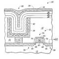
- Construction 10includes a substrate 12 which can comprise, for example, monocrystalline silicon lightly-doped with a p-type background dopant.
- substrate 12can comprise, for example, monocrystalline silicon lightly-doped with a p-type background dopant.
- substrate 12can comprise, for example, monocrystalline silicon lightly-doped with a p-type background dopant.
- substrate 12can comprise, for example, monocrystalline silicon lightly-doped with a p-type background dopant.
- substrate 12can comprise, for example, monocrystalline silicon lightly-doped with a p-type background dopant.
- semiconductor substrateand “semiconductor substrate” are defined to mean any construction comprising semiconductive material, including, but not limited to, bulk semiconductive materials such as a semiconductive wafer (either alone or in assemblies comprising other materials thereon), and semiconductive material layers (either alone or in assemblies comprising other materials).
- substraterefers to any supporting structure, including, but not limited to, the semiconductive substrates described above
- An electrically insulative material 14is formed over substrate 12 .
- Material 14can comprise any suitable material including, for example, borophosphosilicate glass (BPSG), silicon dioxide, silicon nitride, etc.
- An openingextends through insulative material 14 to substrate 12 , and an electrically conductive pedestal 16 is formed within the opening.
- Pedestal 16can comprise any suitable electrically conductive material, including, for example, one or more of conductively-doped silicon, metal, and metal compounds.
- Pedestal 16has an upper surface 17 which defines an electrical node.
- a capacitor construction 18is over pedestal 16 , and an electrode of the capacitor construction is electrically connected with electrical node 17 .
- Pedestal 16can be utilized to electrically connect capacitor construction 18 with other circuitry (not shown).
- the other circuitrycan include, for example, a transistor device, and pedestal 16 can be electrically connected with a source/drain region of such transistor device.
- the capacitor construction 18comprises a first capacitor electrode 20 and a second capacitor electrode 22 .
- the first capacitor electrodecomprises a first electrically conductive layer 24 which can contain any suitable electrically conductive material, including, for example, metal, various metal compounds, and/or conductively-doped silicon.
- the first capacitor electrodealso comprises a second electrically conductive layer 26 over layer 24 .
- Layer 26preferably comprises titanium and nitrogen.
- the layercan, for example, comprise, consist essentially of, or consist of one or both of titanium nitride and boron-doped titanium nitride.
- Second capacitor electrodecomprises an outermost layer 28 which can contain any suitable electrically conductive material, including, for example, conductively-doped silicon, metal, and/or metal compounds.
- Second capacitor electrode 22also comprises an inner electrically conductive layer 30 which preferably contains titanium and nitrogen.
- layer 30can comprise, consist essentially of, or consist of one or both of titanium nitride and boron-doped titanium nitride.
- Capacitor construction 18further comprises a dielectric stack 32 between electrodes 20 and 22 .
- Dielectric stack 32comprises a layer 34 sandwiched between a pair of layers 36 and 38 .
- Layers 36 and 38preferably comprise, consist essentially of, or consist of aluminum oxide.
- Layer 34preferably comprises, consists essentially of, or consists of a high-k dielectric material other than aluminum oxide, and preferably having a dielectric constant greater than that of aluminum oxide.
- layer 34can comprise one or more materials selected from the group consisting of tantalum pentoxide, hafnium oxide, zirconium oxide, barium strontium titanate, strontium titanate, and lead zirconate titanate.
- Construction 10is an exemplary construction, and it is to be understood that the invention encompasses constructions having various modifications relative to the shown construction 10 .
- one or both of conductive layers 24 and 28can be omitted so that one or both of the first and second capacitor electrodes 20 and 22 only comprises a layer containing titanium and nitrogen (i.e., the layers 26 and 30 ).
- the layer 36comprising aluminum oxide between high-k dielectric material 34 and conductive layer 26 , in that the high-k dielectric is typically formed under oxidizing conditions which would oxidize conductive material 26 in the absence of protective aluminum-oxide-containing material 36 .
- second electrode 22is formed after formation of high-k dielectric material 34 , the second electrode will not be oxidized during formation of dielectric material 34 . Accordingly, it can be appropriate in some instances to omit aluminum-oxide-containing material 38 , and form second electrode 22 directly against high-k dielectric material 34 . However, there can be some applications in which leakage between high-k dielectric material 34 and second electrode 22 is problematic if the second electrode is directly against the high-k dielectric material, and in such applications it can be advantageous to form the aluminum-oxide-containing material 38 as a barrier between the high-k dielectric material 34 and the second electrode 22 .
- An exemplary method of forming the construction 10 of FIG. 1is as follows. Initially, a construction comprising substrate 12 having insulative material 14 and pedestal 16 thereover can be formed utilizing conventional methods. The layer 24 of first capacitor electrode 20 can then be formed over an upper surface of pedestal 16 and insulative material 14 utilizing one or more of sputter deposition, chemical vapor deposition and atomic layer deposition, depending on the materials utilized for layer 24 . For instance, if layer 24 comprises conductively-doped silicon, the layer can be formed by chemical vapor deposition of silicon followed by an implant of a suitable conductivity-enhancing dopant into the silicon. If layer 24 comprises metal and/or metal compounds, the layer can be formed by physical vapor deposition, chemical vapor deposition and/or atomic layer deposition.
- the layer 26 containing titanium and nitrogencan be formed by a deposition method.
- An exemplary deposition methodis a chemical vapor deposition process utilizing a metal source and a nitrogen source as precursors, and a temperature of from about 500° C. to about 800° C. It can be preferred that if layer 24 comprises a silicon-containing surface on which layer 26 is to be formed, the surface be exposed to hydrofluoric acid under suitable conditions to remove native oxide from the surface prior to formation of layer 26 . Such can be accomplished by, for example, exposing the surface to a dilute solution of hydrofluoric acid with a 10:1 volumetric ratio of water to 49% hydrofluoric acid.
- an upper surface of a silicon-containing material 24can be subjected to nitridation to increase stack capacitance and decrease leakage.
- the upper surfacecan be subjected to a high temperature rapid thermal nitridation (RTN) process taking place at a temperature of from about 600° C. to about 1200° C., and more preferably from about 800° C. to about 1000° C., for a time of from about 5 seconds to about 60 seconds, and more preferably from about 20 seconds to about 60 seconds.
- RTNrapid thermal nitridation
- the nitridationcan occur by exposing the upper surface to an NH 3 anneal or to an N 2 or ammonia (NH 3 ) plasma processing or other source plasma processing to confer a good interface between conductive layer 24 and the subsequently-formed layer 26 .
- an NH 3 annealor to an N 2 or ammonia (NH 3 ) plasma processing or other source plasma processing to confer a good interface between conductive layer 24 and the subsequently-formed layer 26 .
- NH 3ammonia
- titanium nitrideis an extremely hard material, and almost chemically inert (although it dissolves in hydrofluoric acid), as well as being an excellent conductor. Titanium nitride can also be preferred because it has a high melting point (about 3000° C.), which makes it largely unaffected by high processing temperatures. Further, titanium nitride generally makes excellent ohmic contact with other conductive layers which are directly against the titanium nitride. Boron-doped titanium nitride has advantages similar to those of titanium nitride.
- the deposition of layer 26can occur utilizing ammonia as a nitrogen source; and one or more of titanium tetrachloride (TiCl 4 ), titanium trichloride (TiCl 3 ), and bis (cyclopentadienyl) titanium dichloride (C 5 H 5 ) 2 TiCl 2 ) as a titanium source.
- TiCl 4titanium tetrachloride
- TiCl 3titanium trichloride
- C 5 H 5 ) 2 TiCl 2bis (cyclopentadienyl) titanium dichloride
- layer 26can be formed utilizing low-temperature chemical vapor deposition with methylhydrazine (CH 3 )HNNH 2 ) as a nitrogen source; and one or more of titanium tetrachloride, tetrakis diethylamino titanium (TiN[CH 2 )CH 3 ) 2 ] 5 or tetrakis diemethylamino titanium (Ti[N(CH 3 ) 2 ) 4 ) as a titanium source.
- methylhydrazineCH 3 )HNNH 2
- TiN[CH 2 )CH 3 ) 2 ] 5 or tetrakis diemethylamino titanium (Ti[N(CH 3 ) 2 ) 4 )as a titanium source.
- a titanium nitride material of layer 26can alternatively be formed by atomic layer deposition.
- a first species of precursorwhich can be a titanium source precursor containing chlorine, such as, for example, titanium tetrachloride or titanium trichloride, is first deposited over the surface of layer 24 as a first monolayer.
- a second species of precursorwhich can be, for example, ammonia, is next applied over the monolayer of the first species of precursor. The second species of precursor reacts with the monolayer of the first species of precursor to form a titanium nitride layer.
- Successive layers of titanium nitridecan be formed over layer 24 by sequentially pulsing the first species (which can also be referred to as a first precursor gas) and the second species (which can also be referred to as a second precursor gas).
- the sequence of depositing the monolayers of the first and second species of precursorscan be repeated cycle after cycle and as often as needed, until a desired thickness is reached for the titanium nitride layer 26 .
- a chamber utilized for the atomic layer deposition processcan be exhausted, and, if desired, a pulse of purge gas can be injected into the chamber.
- layer 26comprising boron-doped titanium nitride
- such materialcan have a boron doping concentration of from about 0.01% to about 30% (atomic percentage).
- Incorporation of boron into a titanium nitride filmcan be achieved by exposing a titanium nitride film to B 2 H 6 at a temperature of from about 200° C. to about 600° C., at a pressure of from about 1 Torr to about 1000 Torr, and for a period of time of from about 10 seconds to about 60 minutes. Such can convert the titanium nitride film to a boron-doped titanium material.
- incorporation of boron into a titanium nitride filmcan be achieved by exposing the titanium nitride film to B 2 H 6 and further to ultraviolet (UV) light, at a temperature of from about 200° C. to about 600° C., at a pressure from 1 Torr to about 1000 Torr, and for a period of time of from about 10 seconds to about 60 minutes.
- UVultraviolet
- Any wavelength in the ultraviolet rangecan be used for exposing the B 2 H 6 and furthering incorporating the boron into the titanium nitride material.
- Boron-doped titanium nitridecan also be formed by a deposition method, such as, for example, a chemical vapor deposition process using a titanium source, a boron source and a nitrogen source as precursors.
- the depositioncan be conducted at a temperature of from about 500° C. to about 800° C., and typically is conducted at a temperature of about 600° C.
- the boron-doped titanium nitride layercan be formed using a titanium source precursor containing chlorine, such as, for example, titanium tetrachloride, titanium trichloride, bis(cyclopentadienyl)titanium dichloride and/or cyclopentadienyltitanium trichloride.
- the nitrogen precursorcan comprise, for example, ammonia.
- the boron precursorcan comprise, for example, B 2 H 6 .
- layer 26comprises titanium nitride, boron-doped titanium nitride, or a combination of boron-doped titanium nitride and titanium nitride
- the layerwill typically be formed to a thickness of from about 25 angstroms to about 250 angstroms, with a typical thickness being from about 25 angstroms to about 100 angstroms.
- the layer 26can be subjected to an oxidizing and/or nitridizing ambient to densify the titanium nitride and/or boron-doped titanium nitride. Densification of the material can decrease leakage and increase cell capacitance.
- the oxidizing and/or nitrogen ambientcan also reduce, and in some cases prevent, unwanted diffusion and reactions between material of layer 26 and the material of underlying layer 24 . Additionally, the oxidizing and/or nitridizing can reduce, and preferably prevent, chlorine permeation in the layer 26 .
- the presence of chlorine atoms in layer 26typically occurs as a result of reaction products and materials employed in the chemical vapor deposition processes for formation of the titanium-containing layer.
- An exemplary nitridization processcomprises, for example, one or more of high temperature rapid thermal nitridation (RTN), remote plasma nitridation (RPN), or in-situ remote radio frequency nitridization.
- Layer 26can, for example, be exposed to a nitrogen-containing plasma formed from N 2 and H 2 within a reaction chamber.
- An exemplary nitrogen-containing plasma mixturecomprises, by volume, from about 10% to about 80% of N 2 and from about 20% to about 90% of H 2 , at a temperature of from about 100° C. to about 800° C., and more preferably of from about 100° C. to about 900° C., for an exposure time of from about 30 seconds to about 60 seconds.
- the nitrogen-containing plasma mixturecan further comprise argon or another inert gas, typically in a percentage of from about 0.01% to about 40%, by volume.
- a nitrogen-containing plasma formed from NH 3can be employed with or without an inert gas.
- layer 26can be subjected to an oxidizing ambient.
- layer 26can be subjected to remote plasma oxidation (RPO) using an oxygen or ozone source, with or without ultraviolet light.
- RPOremote plasma oxidation
- Aluminum oxide-containing layer 36can be formed by, for example, chemical vapor deposition, metal-organic chemical vapor deposition, and/or sputtering.
- Layer 36is preferably formed to a thickness of from about 20 angstroms to about 500 angstroms, more preferably from about 25 angstroms to about 100 angstroms, yet more preferably to a thickness of from about 5 angstroms to about 20 angstroms, and in particular applications can be formed to a thickness of from about 5 angstroms to about 10 angstroms.
- the Al 2 O 3 layer 36can also be formed by atomic layer deposition.
- a first species of aluminum precursorsuch as an aluminum source precursor containing chlorine, (for example, aluminum tetrachloride (AlCl 4 ) or aluminum trichloride (AlCl 3 )) is first deposited over the surface of layer 26 .
- An oxygen precursorsuch as, for example, diatomic oxygen (O 2 ) or ozone (O 3 ) is next applied over the monolayer formed from the aluminum-containing precursor.
- the oxygen speciesreacts with the monolayer formed from the aluminum-containing precursor to form an aluminum oxide (Al 2 O 3 ) layer.
- Multiple Al 2 O 3 layerscan be sequentially formed over layer 26 , and the multiple layers can together constitute layer 36 .
- the multiple layerscan be formed by first pulsing the aluminum-comprising species (which can also be referred to as a first precursor gas), and then pulsing the oxygen-containing precursor (which can also be referred to as a second precursor gas) into a reaction chamber to deposit the aluminum oxide layers over layer 26 .
- the sequence of depositing the monolayers of the first and second species of precursorscan be repeated cycle after cycle and as often as needed, until a desired thickness is reached for layer 36 .
- the interior of a reaction chamber utilized for the atomic layer depositioncan be exhausted, and a pulse of purge gas can be provided, if desired.
- High-k dielectric material 34can be formed by any suitable method, including, for example, one or both of chemical vapor deposition and atomic layer deposition.
- the high-k materialis preferably formed to a thickness of from about 50 angstroms to about 100 angstroms.
- the layers 30 and 38 of capacitor 18can be formed utilizing methodology discussed above.
- Aluminum-oxide-containing layer 38can be formed utilizing, for example, the processing described above with reference to layer 36 .
- the layer 30 comprising titanium and nitrogencan be formed utilizing, for example, the processing described previously with reference to layer 26 .
- Layer 28can be formed over layer 30 utilizing any appropriate process, such as, for example, chemical vapor deposition, atomic layer deposition and/or sputter deposition.
- a total thickness of dielectric material 32 of capacitor 18will preferably be from about 40 angstroms to about 100 angstroms, with a thickness of from about 50 angstroms to about 70 angstroms being typical.
- Layer 30can have a thickness approximately the same as that of layer 26 , and can be formed to comprise the same chemical composition as layer 26 . In other aspects of the invention, layer 30 can be formed to have a different chemical composition than layer 26 , and/or can be formed to have a different thickness than layer 26 .
- Construction 10 of FIG. 1illustrates one exemplary capacitor construction of the present invention. Another exemplary capacitor construction of the present invention is described with reference to a construction 50 in FIG. 2 . In referring to FIG. 2 , similar numbering will be utilized as was used above in describing FIG. 1 , where appropriate.
- Construction 50comprises a substrate 12 which can, as discussed above with reference to the construction of FIG. 1 , comprise a semiconductor substrate, and in particular aspects can comprise monocrystalline silicon lightly-doped with a background p-type dopant.
- Transistor device 52is supported by substrate 12 .
- Transistor device 52comprises a transistor gate 54 and source/drain regions 56 and 58 on opposing sides of gate 54 .
- Gate 54can comprise any suitable construction, and is shown comprising an insulative material 60 (which can comprise, for example, silicon dioxide), a conductive material 62 (which can comprise, for example, one or more of conductively-doped silicon, metal and metal compounds), and an insulative cap 64 (which can comprise, for example, one or both of silicon dioxide and silicon nitride).
- Source/drain regions 56 and 58comprise a heavily-doped region 66 and a lightly-doped region 68 inward of the heavily-doped region. Source/drain regions 56 and 58 can be formed by conventional methods.
- a pair of sidewall spacers 70are shown along opposing sidewalls of transistor gate 54 .
- Sidewall spacers 70can comprise, for example, silicon dioxide and/or silicon nitride, and-can be formed by conventional methods.
- Insulative material 72is over substrate 12 and over transistor device 52 .
- Insulative material 72can comprise any suitable material, including, for example, borophosphosilicate glass (BPSG), silicon dioxide, borosilicate glass, and/or phosphosilicate glass.
- BPSGborophosphosilicate glass
- silicon dioxidesilicon dioxide
- borosilicate glasssilicon dioxide
- phosphosilicate glassphosphosilicate glass
- a conductive pedestal 16is within an opening in insulative material 72 , and electrically connected with source/drain region 56 .
- Conductive pedestal 16can comprise the same materials as described above with reference to FIG. 1 .
- a container-type capacitor 80is within an opening in insulative material 72 , and is electrically connected with pedestal 16 .
- Capacitor 80includes a rugged layer 82 , which can correspond to, for example, hemispherical grain polysilicon. Accordingly, layer 82 can be conductively-doped silicon.
- Capacitor 80further comprises the layers 26 , 28 , 30 , 34 , 36 and 38 described previously. Accordingly, the capacitor construction includes a layer 26 comprising titanium and nitrogen, and which can comprise, consist essentially of, or consist of titanium nitride and/or boron-doped titanium nitride.
- the capacitor constructionfurther includes an aluminum oxide-containing layer 36 over the layer 26 , and a high-k dielectric material 34 over the layer 36 .
- the constructionfurther includes a second aluminum oxide-containing layer 38 over high-k dielectric material 34 , and a layer 30 comprising titanium and nitrogen over layer 38 .
- the shown capacitor constructionincludes a conductive material 28 over layer 30 . Layers 28 and 30 together form one of the capacitor electrodes of capacitor 80 , and layers 26 and 82 form the other capacitor electrode of capacitor 80 .
- the source/drain region 58is electrically connected to a bitline 82 . Such connection can occur before or after formation of capacitor 80 .
- the construction 50 comprising capacitor 80 connected to bitline 82 through access device 52corresponds to an exemplary DRAM cell that can be formed in accordance with the present invention.
- a circuit device comprising rugged material formed in accordance with methodology of the present inventioncan be utilized in numerous assemblies, including, for example, computer systems and other electronic systems.
- FIG. 3illustrates generally, by way of example, but not by way of limitation, an embodiment of a computer system 400 according to an aspect of the present invention.
- Computer system 400includes a monitor 401 or other communication output device, a keyboard 402 or other communication input device, and a motherboard 404 .
- Motherboard 404can carry a microprocessor 406 or other data processing unit, and at least one memory device 408 .
- Memory device 408can comprise various aspects of the invention described above, including, for example, the DRAM unit cell described with reference to FIG. 2 .
- Memory device 408can comprise an array of memory cells, and such array can be coupled with addressing circuitry for accessing individual memory cells in the array. Further, the memory cell array can be coupled to a read circuit for reading data from the memory cells.
- the addressing and read circuitrycan be utilized for conveying information between memory device 408 and processor 406 . Such is illustrated in the block diagram of the motherboard 404 shown in FIG. 4 . In such block diagram, the addressing circuitry is illustrated as 410 and the read circuitry is illustrated as 412 .
- memory device 408can correspond to a memory module.
- SIMMssingle in-line memory modules
- DIMMsdual in-line memory modules
- the memory devicecan be incorporated into any of a variety of designs which provide different methods of reading from and writing to memory cells of the device.
- One such methodis the page mode operation.
- Page mode operations in a DRAMare defined by the method of accessing a row of a memory cell arrays and randomly accessing different columns of the array. Data stored at the row and column intersection can be read and output while that column is accessed.
- EDOextended data output
- FIG. 5illustrates a simplified block diagram of a high-level organization of various embodiments of an exemplary electronic system 700 of the present invention.
- System 700can correspond to, for example, a computer system, a process control system, or any other system that employs a processor and associated memory.
- Electronic system 700has functional elements, including a processor or arithmetic/logic unit (ALU) 702 , a control unit 704 , a memory device unit 706 and an input/output (I/O) device 708 .
- ALUarithmetic/logic unit
- control unit 704controls the a memory device unit 706
- I/Oinput/output
- electronic system 700will have a native set of instructions that specify operations to be performed on data by the processor 702 and other interactions between the processor 702 , the memory device unit 706 and the I/O devices 708 .
- the control unit 704coordinates all operations of the processor 702 , the memory device 706 and the I/O devices 708 by continuously cycling through a set of operations that cause instructions to be fetched from the memory device 706 and executed.
- the memory device 706includes, but is not limited to, random access memory (RAM) devices, read-only memory (ROM) devices, and peripheral devices such as a floppy disk drive and a compact disk CD-ROM drive.
- RAMrandom access memory
- ROMread-only memory
- peripheral devicessuch as a floppy disk drive and a compact disk CD-ROM drive.
- FIG. 6is a simplified block diagram of a high-level organization of various embodiments of an exemplary electronic system 800 .
- the system 800includes a memory device 802 that has an array of memory cells 804 , address decoder 806 , row access circuitry 808 , column access circuitry 810 , read/write control circuitry 812 for controlling operations, and input/output circuitry 814 .
- the memory device 802further includes power circuitry 816 , and sensors 820 , such as current sensors for determining whether a memory cell is in a low-threshold conducting state or in a high-threshold non-conducting state.
- the illustrated power circuitry 816includes power supply circuitry 880 , circuitry 882 for providing a reference voltage, circuitry 884 for providing the first wordline with pulses, circuitry 886 for providing the second wordline with pulses, and circuitry 888 for providing the bitline with pulses.
- the system 800also includes a processor 822 , or memory controller for memory accessing.
- the memory device 802receives control signals 824 from the processor 822 over wiring or metallization lines.
- the memory device 802is used to store data which is accessed via I/O lines. It will be appreciated by those skilled in the art that additional circuitry and control signals can be provided, and that the memory device 802 has been simplified to help focus on the invention.
- At least one of the processor 822 or memory device 802can include a DRAM cell of the type described previously in this disclosure.
- Applications for memory cellscan include electronic systems for use in memory modules, device drivers, power modules, communication modems, processor modules, and application-specific modules, and may include multilayer, multichip modules.
- Such circuitrycan further be a subcomponent of a variety of electronic systems, such as a clock, a television, a cell phone, a personal computer, an automobile, an industrial control system, an aircraft, and others.
Landscapes
- Engineering & Computer Science (AREA)
- Power Engineering (AREA)
- Microelectronics & Electronic Packaging (AREA)
- Manufacturing & Machinery (AREA)
- Ceramic Engineering (AREA)
- Chemical & Material Sciences (AREA)
- Inorganic Chemistry (AREA)
- Semiconductor Memories (AREA)
Abstract
Description
- The invention pertains to capacitor constructions and methods of forming capacitor constructions.
- Capacitor constructions are common circuit devices. Capacitor constructions are utilized in, for example, dynamic random access memory (DRAM) cells of integrated circuits. The DRAM cells typically comprise a charge storage capacitor coupled to an access device, with the typical access device being a metal-oxide-semiconductor field effect transistor (MOSFET).
- A continuing goal in integrated circuit device fabrication is to increase performance of circuit devices without increasing the amount of real estate consumed by the devices. For capacitor devices, such goal can manifest as a desire to increase the total charge capacity of a capacitor device without significantly affecting the cell area consumed by the device. New capacitor dielectric materials with high dielectric constants (so-called high-k materials) have been introduced to replace conventional dielectric materials, such as, for example, silicon nitride and silicon dioxide. Thin films of the high-k materials can be utilized in capacitor devices to obtain high capacitance while maintaining, or even reducing, the footprint of the devices relative to previous devices that utilized lower k dielectric materials.
- High-k dielectric materials are typically understood to be materials having a dielectric constant greater than that of silicon dioxide, with exemplary high-k materials being Al2O3(aluminum oxide), Ta2O5(tantalum pentoxide), barium titanate (BT), strontium titanate (ST), lead zirconate titanate (PZT), bismuth strontium titanate (BST), HfOx(hafnium oxide) and ZrOy(zirconium oxide). The x in HfOxand the y in ZrOyare numbers greater than zero, and typically less than or equal to 2.
- Although the high-k dielectric materials described above can provide numerous advantages when utilized in capacitor constructions, there are difficulties associated with the materials which can offset the benefits gained by utilizing the materials. One problem encountered when incorporating high-k materials into current DRAM cell designs is that chemical reactivity between the high-k materials and other materials of a DRAM cell can impede performance of the cell, and even destroy operability of the cell. For instance, numerous of the high-k materials are formed under strongly oxidizing conditions, and such conditions can oxidize electrode components which are intended to be incorporated into capacitor constructions with the high-k materials. The oxidized electrode components can have reduced electrical conductivity relative to non-oxidized components, which can impair operability of the resulting capacitor cell, and in some cases can lower the total capacitance of resulting capacitor below acceptable tolerances.
- It would be desirable to develop new methods for incorporating high-k dielectric materials into capacitor constructions.
- In one aspect, the invention encompasses a capacitor construction which includes a first capacitor electrode having a layer comprising titanium and nitrogen. A layer comprising aluminum oxide is over the layer comprising titanium and nitrogen, and a high-k dielectric material other than aluminum oxide is over the layer comprising aluminum oxide. A second capacitor electrode is over the high-k dielectric material.
- In another aspect, the invention encompasses a capacitor construction comprising a high-k dielectric material, two layers which include titanium and nitrogen, and two layers which include aluminum oxide. The high-k dielectric material is between the two layers which comprise aluminum oxide, and the two layers comprising aluminum oxide are in turn between the two layers comprising titanium and nitrogen.
- In another aspect, the invention encompasses methods of forming capacitor constructions.
- The capacitor constructions of the present invention can be incorporated into DRAM cells and electronic systems.
- Preferred embodiments of the invention are described below with reference to the following accompanying drawings.
FIG. 1 is a diagrammatic, cross-sectional view of a capacitor construction formed in accordance with an exemplary aspect of the present invention.FIG. 2 is a diagrammatic, cross-sectional view of a capacitor construction formed in accordance with another exemplary aspect of the present invention.FIG. 3 is a diagrammatic view of a computer illustrating an exemplary application of the present invention.FIG. 4 is a block diagram showing particular features of the motherboard of theFIG. 3 computer.FIG. 5 is a high-level block diagram of an electronic system according to an exemplary aspect of the present invention.FIG. 6 is a simplified block diagram of an exemplary electronic system according to an aspect of the present invention.- This disclosure of the invention is submitted in furtherance of the constitutional purposes of the U.S. Patent Laws “to promote the progress of science and useful arts” (Article 1, Section 8).
- The invention includes a recognition that it can be useful to utilize aluminum oxide (Al2O3) dielectric material as a barrier layer between a capacitor electrode and a high-k dielectric material other than aluminum oxide in applications in which the capacitor electrode comprises titanium and nitrogen. In particular applications, the capacitor electrode can comprise one or both of titanium nitride (TiN) and boron-doped titanium nitride (TiBN). The high-k dielectric material can comprise, for example, one or more of Ta2O5, HfOx, ZrOy, barium strontium titanate, strontium titanate, and lead zirconate titanate, where x and y are numbers greater than 0. The capacitor constructions can be metal insulator metal (MIM) constructions, and in particular aspects both electrodes of the capacitor constructions can comprise titanium and nitrogen; and both electrodes can separated from the high-k dielectric material by layers of aluminum oxide.
- There are several advantages to utilizing a dielectric comprising at least one aluminum oxide portion together with at least one portion that is a high-k dielectric material other than aluminum oxide. It can be preferred that the high-k dielectric material have a dielectric constant greater than aluminum oxide to improve the capacitance per unit area that can be obtained with a capacitor construction of the present invention. The high-k dielectric materials other than aluminum oxide can significantly improve the permittivity of a stack relative to a dielectric utilizing aluminum oxide alone. For instance, crystalline tantalum pentoxide can have permittivity values of from 30 to 100, which is significantly higher than the aluminum oxide permittivity, (typically from about 9 to about 11). The aluminum oxide layers can avoid oxidation of the capacitor electrodes and other problems which would occur if the high-k dielectric material were utilized in the absence of the aluminum oxide layers.
- The utilization of electrodes comprising titanium nitride and/or boron-doped titanium nitride can be particularly advantageous in applications of the present invention. Specifically, titanium nitride and/or boron-doped titanium nitride can be readily formed over a diverse range of materials, and further can be conformally formed over the materials. Further, aluminum oxide can be readily conformally formed over layers comprising one or both of TiN and TiBN, which can enable methodology of the present invention to be readily integrated into a diverse range of semiconductor fabrication processes.
- An exemplary aspect of the invention is described with reference to a
semiconductor construction 10 inFIG. 1 .Construction 10 includes asubstrate 12 which can comprise, for example, monocrystalline silicon lightly-doped with a p-type background dopant. To aid in interpretation of the claims that follow, the terms “semiconductive substrate” and “semiconductor substrate” are defined to mean any construction comprising semiconductive material, including, but not limited to, bulk semiconductive materials such as a semiconductive wafer (either alone or in assemblies comprising other materials thereon), and semiconductive material layers (either alone or in assemblies comprising other materials). The term “substrate” refers to any supporting structure, including, but not limited to, the semiconductive substrates described above. - An electrically
insulative material 14 is formed oversubstrate 12.Material 14 can comprise any suitable material including, for example, borophosphosilicate glass (BPSG), silicon dioxide, silicon nitride, etc. An opening extends throughinsulative material 14 tosubstrate 12, and an electricallyconductive pedestal 16 is formed within the opening.Pedestal 16 can comprise any suitable electrically conductive material, including, for example, one or more of conductively-doped silicon, metal, and metal compounds.Pedestal 16 has anupper surface 17 which defines an electrical node. - A
capacitor construction 18 is overpedestal 16, and an electrode of the capacitor construction is electrically connected withelectrical node 17.Pedestal 16 can be utilized to electrically connectcapacitor construction 18 with other circuitry (not shown). The other circuitry can include, for example, a transistor device, andpedestal 16 can be electrically connected with a source/drain region of such transistor device. - The
capacitor construction 18 comprises afirst capacitor electrode 20 and asecond capacitor electrode 22. The first capacitor electrode comprises a first electricallyconductive layer 24 which can contain any suitable electrically conductive material, including, for example, metal, various metal compounds, and/or conductively-doped silicon. The first capacitor electrode also comprises a second electricallyconductive layer 26 overlayer 24.Layer 26 preferably comprises titanium and nitrogen. The layer can, for example, comprise, consist essentially of, or consist of one or both of titanium nitride and boron-doped titanium nitride. - Second capacitor electrode comprises an
outermost layer 28 which can contain any suitable electrically conductive material, including, for example, conductively-doped silicon, metal, and/or metal compounds.Second capacitor electrode 22 also comprises an inner electricallyconductive layer 30 which preferably contains titanium and nitrogen. In particular aspects,layer 30 can comprise, consist essentially of, or consist of one or both of titanium nitride and boron-doped titanium nitride. Capacitor construction 18 further comprises adielectric stack 32 betweenelectrodes Dielectric stack 32 comprises alayer 34 sandwiched between a pair oflayers Layers Layer 34 preferably comprises, consists essentially of, or consists of a high-k dielectric material other than aluminum oxide, and preferably having a dielectric constant greater than that of aluminum oxide. In particular aspects,layer 34 can comprise one or more materials selected from the group consisting of tantalum pentoxide, hafnium oxide, zirconium oxide, barium strontium titanate, strontium titanate, and lead zirconate titanate.Construction 10 is an exemplary construction, and it is to be understood that the invention encompasses constructions having various modifications relative to the shownconstruction 10. For instance, one or both ofconductive layers second capacitor electrodes layers 26 and30). Also, there can be particular advantages to forming thelayer 36 comprising aluminum oxide between high-k dielectric material 34 andconductive layer 26, in that the high-k dielectric is typically formed under oxidizing conditions which would oxidizeconductive material 26 in the absence of protective aluminum-oxide-containingmaterial 36. However, sincesecond electrode 22 is formed after formation of high-k dielectric material 34, the second electrode will not be oxidized during formation ofdielectric material 34. Accordingly, it can be appropriate in some instances to omit aluminum-oxide-containingmaterial 38, and formsecond electrode 22 directly against high-k dielectric material 34. However, there can be some applications in which leakage between high-k dielectric material 34 andsecond electrode 22 is problematic if the second electrode is directly against the high-k dielectric material, and in such applications it can be advantageous to form the aluminum-oxide-containingmaterial 38 as a barrier between the high-k dielectric material 34 and thesecond electrode 22.- An exemplary method of forming the
construction 10 ofFIG. 1 is as follows. Initially, aconstruction comprising substrate 12 havinginsulative material 14 andpedestal 16 thereover can be formed utilizing conventional methods. Thelayer 24 offirst capacitor electrode 20 can then be formed over an upper surface ofpedestal 16 andinsulative material 14 utilizing one or more of sputter deposition, chemical vapor deposition and atomic layer deposition, depending on the materials utilized forlayer 24. For instance, iflayer 24 comprises conductively-doped silicon, the layer can be formed by chemical vapor deposition of silicon followed by an implant of a suitable conductivity-enhancing dopant into the silicon. Iflayer 24 comprises metal and/or metal compounds, the layer can be formed by physical vapor deposition, chemical vapor deposition and/or atomic layer deposition. - The
layer 26 containing titanium and nitrogen can be formed by a deposition method. An exemplary deposition method is a chemical vapor deposition process utilizing a metal source and a nitrogen source as precursors, and a temperature of from about 500° C. to about 800° C. It can be preferred that iflayer 24 comprises a silicon-containing surface on whichlayer 26 is to be formed, the surface be exposed to hydrofluoric acid under suitable conditions to remove native oxide from the surface prior to formation oflayer 26. Such can be accomplished by, for example, exposing the surface to a dilute solution of hydrofluoric acid with a 10:1 volumetric ratio of water to 49% hydrofluoric acid. Additionally, and/or alternatively, an upper surface of a silicon-containingmaterial 24 can be subjected to nitridation to increase stack capacitance and decrease leakage. Specifically, the upper surface can be subjected to a high temperature rapid thermal nitridation (RTN) process taking place at a temperature of from about 600° C. to about 1200° C., and more preferably from about 800° C. to about 1000° C., for a time of from about 5 seconds to about 60 seconds, and more preferably from about 20 seconds to about 60 seconds. Alternatively, the nitridation can occur by exposing the upper surface to an NH3anneal or to an N2or ammonia (NH3) plasma processing or other source plasma processing to confer a good interface betweenconductive layer 24 and the subsequently-formedlayer 26. - Among the advantages for utilizing titanium nitride for
layer 26 is that titanium nitride is an extremely hard material, and almost chemically inert (although it dissolves in hydrofluoric acid), as well as being an excellent conductor. Titanium nitride can also be preferred because it has a high melting point (about 3000° C.), which makes it largely unaffected by high processing temperatures. Further, titanium nitride generally makes excellent ohmic contact with other conductive layers which are directly against the titanium nitride. Boron-doped titanium nitride has advantages similar to those of titanium nitride. - The deposition of
layer 26 can occur utilizing ammonia as a nitrogen source; and one or more of titanium tetrachloride (TiCl4), titanium trichloride (TiCl3), and bis (cyclopentadienyl) titanium dichloride (C5H5)2TiCl2) as a titanium source. Alternatively,layer 26 can be formed utilizing low-temperature chemical vapor deposition with methylhydrazine (CH3)HNNH2) as a nitrogen source; and one or more of titanium tetrachloride, tetrakis diethylamino titanium (TiN[CH2)CH3)2]5or tetrakis diemethylamino titanium (Ti[N(CH3)2)4) as a titanium source. - A titanium nitride material of
layer 26 can alternatively be formed by atomic layer deposition. For example, a first species of precursor, which can be a titanium source precursor containing chlorine, such as, for example, titanium tetrachloride or titanium trichloride, is first deposited over the surface oflayer 24 as a first monolayer. A second species of precursor, which can be, for example, ammonia, is next applied over the monolayer of the first species of precursor. The second species of precursor reacts with the monolayer of the first species of precursor to form a titanium nitride layer. Successive layers of titanium nitride can be formed overlayer 24 by sequentially pulsing the first species (which can also be referred to as a first precursor gas) and the second species (which can also be referred to as a second precursor gas). The sequence of depositing the monolayers of the first and second species of precursors can be repeated cycle after cycle and as often as needed, until a desired thickness is reached for thetitanium nitride layer 26. Between each of the precursor gas pulses, a chamber utilized for the atomic layer deposition process can be exhausted, and, if desired, a pulse of purge gas can be injected into the chamber. - If
layer 26 comprising boron-doped titanium nitride, such material can have a boron doping concentration of from about 0.01% to about 30% (atomic percentage). Incorporation of boron into a titanium nitride film can be achieved by exposing a titanium nitride film to B2H6at a temperature of from about 200° C. to about 600° C., at a pressure of from about 1 Torr to about 1000 Torr, and for a period of time of from about 10 seconds to about 60 minutes. Such can convert the titanium nitride film to a boron-doped titanium material. Alternatively, incorporation of boron into a titanium nitride film can be achieved by exposing the titanium nitride film to B2H6and further to ultraviolet (UV) light, at a temperature of from about 200° C. to about 600° C., at a pressure from 1 Torr to about 1000 Torr, and for a period of time of from about 10 seconds to about 60 minutes. Any wavelength in the ultraviolet range can be used for exposing the B2H6and furthering incorporating the boron into the titanium nitride material. - Boron-doped titanium nitride can also be formed by a deposition method, such as, for example, a chemical vapor deposition process using a titanium source, a boron source and a nitrogen source as precursors. The deposition can be conducted at a temperature of from about 500° C. to about 800° C., and typically is conducted at a temperature of about 600° C. The boron-doped titanium nitride layer can be formed using a titanium source precursor containing chlorine, such as, for example, titanium tetrachloride, titanium trichloride, bis(cyclopentadienyl)titanium dichloride and/or cyclopentadienyltitanium trichloride. The nitrogen precursor can comprise, for example, ammonia. The boron precursor can comprise, for example, B2H6.
- Regardless of whether
layer 26 comprises titanium nitride, boron-doped titanium nitride, or a combination of boron-doped titanium nitride and titanium nitride, the layer will typically be formed to a thickness of from about 25 angstroms to about 250 angstroms, with a typical thickness being from about 25 angstroms to about 100 angstroms. - After formation of titanium nitride and/or boron-doped
titanium nitride layer 26, thelayer 26 can be subjected to an oxidizing and/or nitridizing ambient to densify the titanium nitride and/or boron-doped titanium nitride. Densification of the material can decrease leakage and increase cell capacitance. The oxidizing and/or nitrogen ambient can also reduce, and in some cases prevent, unwanted diffusion and reactions between material oflayer 26 and the material ofunderlying layer 24. Additionally, the oxidizing and/or nitridizing can reduce, and preferably prevent, chlorine permeation in thelayer 26. The presence of chlorine atoms inlayer 26 typically occurs as a result of reaction products and materials employed in the chemical vapor deposition processes for formation of the titanium-containing layer. - An exemplary nitridization process comprises, for example, one or more of high temperature rapid thermal nitridation (RTN), remote plasma nitridation (RPN), or in-situ remote radio frequency nitridization.
Layer 26 can, for example, be exposed to a nitrogen-containing plasma formed from N2and H2within a reaction chamber. An exemplary nitrogen-containing plasma mixture comprises, by volume, from about 10% to about 80% of N2and from about 20% to about 90% of H2, at a temperature of from about 100° C. to about 800° C., and more preferably of from about 100° C. to about 900° C., for an exposure time of from about 30 seconds to about 60 seconds. The nitrogen-containing plasma mixture can further comprise argon or another inert gas, typically in a percentage of from about 0.01% to about 40%, by volume. Alternatively, a nitrogen-containing plasma formed from NH3can be employed with or without an inert gas. In yet another aspect of the invention,layer 26 can be subjected to an oxidizing ambient. For example,layer 26 can be subjected to remote plasma oxidation (RPO) using an oxygen or ozone source, with or without ultraviolet light. - Aluminum oxide-containing
layer 36 can be formed by, for example, chemical vapor deposition, metal-organic chemical vapor deposition, and/or sputtering.Layer 36 is preferably formed to a thickness of from about 20 angstroms to about 500 angstroms, more preferably from about 25 angstroms to about 100 angstroms, yet more preferably to a thickness of from about 5 angstroms to about 20 angstroms, and in particular applications can be formed to a thickness of from about 5 angstroms to about 10 angstroms. - The Al2O3layer36 can also be formed by atomic layer deposition. In an exemplary process, a first species of aluminum precursor, such as an aluminum source precursor containing chlorine, (for example, aluminum tetrachloride (AlCl4) or aluminum trichloride (AlCl3)) is first deposited over the surface of
layer 26. An oxygen precursor, such as, for example, diatomic oxygen (O2) or ozone (O3) is next applied over the monolayer formed from the aluminum-containing precursor. The oxygen species reacts with the monolayer formed from the aluminum-containing precursor to form an aluminum oxide (Al2O3) layer. Multiple Al2O3layers can be sequentially formed overlayer 26, and the multiple layers can together constitutelayer 36. The multiple layers can be formed by first pulsing the aluminum-comprising species (which can also be referred to as a first precursor gas), and then pulsing the oxygen-containing precursor (which can also be referred to as a second precursor gas) into a reaction chamber to deposit the aluminum oxide layers overlayer 26. The sequence of depositing the monolayers of the first and second species of precursors can be repeated cycle after cycle and as often as needed, until a desired thickness is reached forlayer 36. Between each of the precursor gas pulses, the interior of a reaction chamber utilized for the atomic layer deposition can be exhausted, and a pulse of purge gas can be provided, if desired. - High-
k dielectric material 34 can be formed by any suitable method, including, for example, one or both of chemical vapor deposition and atomic layer deposition. The high-k material is preferably formed to a thickness of from about 50 angstroms to about 100 angstroms. - The
layers capacitor 18 can be formed utilizing methodology discussed above. Aluminum-oxide-containinglayer 38 can be formed utilizing, for example, the processing described above with reference tolayer 36. Thelayer 30 comprising titanium and nitrogen can be formed utilizing, for example, the processing described previously with reference tolayer 26. Layer 28 can be formed overlayer 30 utilizing any appropriate process, such as, for example, chemical vapor deposition, atomic layer deposition and/or sputter deposition.- A total thickness of
dielectric material 32 ofcapacitor 18 will preferably be from about 40 angstroms to about 100 angstroms, with a thickness of from about 50 angstroms to about 70 angstroms being typical.Layer 30 can have a thickness approximately the same as that oflayer 26, and can be formed to comprise the same chemical composition aslayer 26. In other aspects of the invention,layer 30 can be formed to have a different chemical composition thanlayer 26, and/or can be formed to have a different thickness thanlayer 26. Construction 10 ofFIG. 1 illustrates one exemplary capacitor construction of the present invention. Another exemplary capacitor construction of the present invention is described with reference to aconstruction 50 inFIG. 2 . In referring toFIG. 2 , similar numbering will be utilized as was used above in describingFIG. 1 , where appropriate.Construction 50 comprises asubstrate 12 which can, as discussed above with reference to the construction ofFIG. 1 , comprise a semiconductor substrate, and in particular aspects can comprise monocrystalline silicon lightly-doped with a background p-type dopant.- A
transistor device 52 is supported bysubstrate 12.Transistor device 52 comprises atransistor gate 54 and source/drain regions gate 54.Gate 54 can comprise any suitable construction, and is shown comprising an insulative material60 (which can comprise, for example, silicon dioxide), a conductive material62 (which can comprise, for example, one or more of conductively-doped silicon, metal and metal compounds), and an insulative cap64 (which can comprise, for example, one or both of silicon dioxide and silicon nitride). - Source/
drain regions region 66 and a lightly-dopedregion 68 inward of the heavily-doped region. Source/drain regions - A pair of
sidewall spacers 70 are shown along opposing sidewalls oftransistor gate 54.Sidewall spacers 70 can comprise, for example, silicon dioxide and/or silicon nitride, and-can be formed by conventional methods. - An
insulative material 72 is oversubstrate 12 and overtransistor device 52.Insulative material 72 can comprise any suitable material, including, for example, borophosphosilicate glass (BPSG), silicon dioxide, borosilicate glass, and/or phosphosilicate glass. - A
conductive pedestal 16 is within an opening ininsulative material 72, and electrically connected with source/drain region 56.Conductive pedestal 16 can comprise the same materials as described above with reference toFIG. 1 . - A container-
type capacitor 80 is within an opening ininsulative material 72, and is electrically connected withpedestal 16.Capacitor 80 includes arugged layer 82, which can correspond to, for example, hemispherical grain polysilicon. Accordingly,layer 82 can be conductively-doped silicon. Capacitor 80 further comprises thelayers layer 26 comprising titanium and nitrogen, and which can comprise, consist essentially of, or consist of titanium nitride and/or boron-doped titanium nitride. The capacitor construction further includes an aluminum oxide-containinglayer 36 over thelayer 26, and a high-k dielectric material 34 over thelayer 36. The construction further includes a second aluminum oxide-containinglayer 38 over high-k dielectric material 34, and alayer 30 comprising titanium and nitrogen overlayer 38. Additionally, the shown capacitor construction includes aconductive material 28 overlayer 30.Layers capacitor 80, and layers26 and82 form the other capacitor electrode ofcapacitor 80.- The source/
drain region 58 is electrically connected to abitline 82. Such connection can occur before or after formation ofcapacitor 80. Theconstruction 50 comprisingcapacitor 80 connected to bitline82 throughaccess device 52 corresponds to an exemplary DRAM cell that can be formed in accordance with the present invention. - Although the exemplary construction as shown utilizing a container-type capacitor, it is to be understood that methodology of the present invention can be utilized to form other capacitors, such as, for example, stud capacitors.
- A circuit device comprising rugged material formed in accordance with methodology of the present invention (such as the above-described DRAM cell) can be utilized in numerous assemblies, including, for example, computer systems and other electronic systems.
FIG. 3 illustrates generally, by way of example, but not by way of limitation, an embodiment of acomputer system 400 according to an aspect of the present invention.Computer system 400 includes amonitor 401 or other communication output device, akeyboard 402 or other communication input device, and amotherboard 404.Motherboard 404 can carry amicroprocessor 406 or other data processing unit, and at least onememory device 408.Memory device 408 can comprise various aspects of the invention described above, including, for example, the DRAM unit cell described with reference toFIG. 2 .Memory device 408 can comprise an array of memory cells, and such array can be coupled with addressing circuitry for accessing individual memory cells in the array. Further, the memory cell array can be coupled to a read circuit for reading data from the memory cells. The addressing and read circuitry can be utilized for conveying information betweenmemory device 408 andprocessor 406. Such is illustrated in the block diagram of themotherboard 404 shown inFIG. 4 . In such block diagram, the addressing circuitry is illustrated as410 and the read circuitry is illustrated as412.- In particular aspects of the invention,
memory device 408 can correspond to a memory module. For example, single in-line memory modules (SIMMs) and dual in-line memory modules (DIMMs) may be used in the implementation which utilizes the teachings of the present invention. The memory device can be incorporated into any of a variety of designs which provide different methods of reading from and writing to memory cells of the device. One such method is the page mode operation. Page mode operations in a DRAM are defined by the method of accessing a row of a memory cell arrays and randomly accessing different columns of the array. Data stored at the row and column intersection can be read and output while that column is accessed. - An alternate type of device is the extended data output (EDO) memory which allows data stored at a memory array address to be available as output after the addressed column has been closed. This memory can increase some communication speeds by allowing shorter access signals without reducing the time in which memory output data is available on a memory bus. Other alternative types of devices include SDRAM, DDR SDRAM, SLDRAM, VRAM and Direct RDRAM, as well as others such as SRAM or Flash memories.
FIG. 5 illustrates a simplified block diagram of a high-level organization of various embodiments of an exemplaryelectronic system 700 of the present invention.System 700 can correspond to, for example, a computer system, a process control system, or any other system that employs a processor and associated memory.Electronic system 700 has functional elements, including a processor or arithmetic/logic unit (ALU)702, acontrol unit 704, amemory device unit 706 and an input/output (I/O)device 708. Generally,electronic system 700 will have a native set of instructions that specify operations to be performed on data by theprocessor 702 and other interactions between theprocessor 702, thememory device unit 706 and the I/O devices 708. Thecontrol unit 704 coordinates all operations of theprocessor 702, thememory device 706 and the I/O devices 708 by continuously cycling through a set of operations that cause instructions to be fetched from thememory device 706 and executed. In various embodiments, thememory device 706 includes, but is not limited to, random access memory (RAM) devices, read-only memory (ROM) devices, and peripheral devices such as a floppy disk drive and a compact disk CD-ROM drive. One of ordinary skill in the art will understand, upon reading and comprehending this disclosure, that any of the illustrated electrical components are capable of being fabricated to include one or more DRAM cells in accordance with various aspects of the present invention.FIG. 6 is a simplified block diagram of a high-level organization of various embodiments of an exemplaryelectronic system 800. Thesystem 800 includes amemory device 802 that has an array ofmemory cells 804,address decoder 806,row access circuitry 808,column access circuitry 810, read/writecontrol circuitry 812 for controlling operations, and input/output circuitry 814. Thememory device 802 further includespower circuitry 816, andsensors 820, such as current sensors for determining whether a memory cell is in a low-threshold conducting state or in a high-threshold non-conducting state. The illustratedpower circuitry 816 includespower supply circuitry 880,circuitry 882 for providing a reference voltage,circuitry 884 for providing the first wordline with pulses,circuitry 886 for providing the second wordline with pulses, andcircuitry 888 for providing the bitline with pulses. Thesystem 800 also includes aprocessor 822, or memory controller for memory accessing.- The
memory device 802 receives control signals824 from theprocessor 822 over wiring or metallization lines. Thememory device 802 is used to store data which is accessed via I/O lines. It will be appreciated by those skilled in the art that additional circuitry and control signals can be provided, and that thememory device 802 has been simplified to help focus on the invention. At least one of theprocessor 822 ormemory device 802 can include a DRAM cell of the type described previously in this disclosure. - The various illustrated systems of this disclosure are intended to provide a general understanding of various applications for the circuitry and structures of the present invention, and are not intended to serve as a complete description of all the elements and features of an electronic system using memory cells in accordance with aspects of the present invention. One of ordinary skill in the art will understand that the various electronic systems can be fabricated in single-package processing units, or even on a single semiconductor chip, in order to reduce the communication time between the processor and the memory device(s).
- Applications for memory cells can include electronic systems for use in memory modules, device drivers, power modules, communication modems, processor modules, and application-specific modules, and may include multilayer, multichip modules. Such circuitry can further be a subcomponent of a variety of electronic systems, such as a clock, a television, a cell phone, a personal computer, an automobile, an industrial control system, an aircraft, and others.
- In compliance with the statute, the invention has been described in language more or less specific as to structural and methodical features. It is to be understood, however, that the invention is not limited to the specific features shown and described, since the means herein disclosed comprise preferred forms of putting the invention into effect. The invention is, therefore, claimed in any of its forms or modifications within the proper scope of the appended claims appropriately interpreted in accordance with the doctrine of equivalents.
Claims (46)
Priority Applications (1)
| Application Number | Priority Date | Filing Date | Title |
|---|---|---|---|
| US11/504,935US7535695B2 (en) | 2003-05-20 | 2006-08-15 | DRAM cells and electronic systems |
Applications Claiming Priority (2)
| Application Number | Priority Date | Filing Date | Title |
|---|---|---|---|
| US10/442,509US7092234B2 (en) | 2003-05-20 | 2003-05-20 | DRAM cells and electronic systems |
| US11/504,935US7535695B2 (en) | 2003-05-20 | 2006-08-15 | DRAM cells and electronic systems |
Related Parent Applications (1)
| Application Number | Title | Priority Date | Filing Date |
|---|---|---|---|
| US10/442,509ContinuationUS7092234B2 (en) | 2003-05-20 | 2003-05-20 | DRAM cells and electronic systems |
Publications (2)
| Publication Number | Publication Date |
|---|---|
| US20060274477A1true US20060274477A1 (en) | 2006-12-07 |
| US7535695B2 US7535695B2 (en) | 2009-05-19 |
Family
ID=33450214
Family Applications (3)
| Application Number | Title | Priority Date | Filing Date |
|---|---|---|---|
| US10/442,509Expired - LifetimeUS7092234B2 (en) | 2003-05-20 | 2003-05-20 | DRAM cells and electronic systems |
| US10/756,621Expired - LifetimeUS7033884B2 (en) | 2003-05-20 | 2004-01-12 | Methods of forming capacitor constructions |
| US11/504,935Expired - LifetimeUS7535695B2 (en) | 2003-05-20 | 2006-08-15 | DRAM cells and electronic systems |
Family Applications Before (2)
| Application Number | Title | Priority Date | Filing Date |
|---|---|---|---|
| US10/442,509Expired - LifetimeUS7092234B2 (en) | 2003-05-20 | 2003-05-20 | DRAM cells and electronic systems |
| US10/756,621Expired - LifetimeUS7033884B2 (en) | 2003-05-20 | 2004-01-12 | Methods of forming capacitor constructions |
Country Status (1)
| Country | Link |
|---|---|
| US (3) | US7092234B2 (en) |
Cited By (2)
| Publication number | Priority date | Publication date | Assignee | Title |
|---|---|---|---|---|
| US20060273426A1 (en)* | 2005-05-17 | 2006-12-07 | Elpida Memory, Inc. | Semiconductor device and method for manufacturing semiconductor device |
| US20140091426A1 (en)* | 2009-11-13 | 2014-04-03 | Taiwan Semiconductor Manufacturing Company, Ltd. | Capacitor and Method for Making Same |
Families Citing this family (36)
| Publication number | Priority date | Publication date | Assignee | Title |
|---|---|---|---|---|
| US7192827B2 (en)* | 2001-01-05 | 2007-03-20 | Micron Technology, Inc. | Methods of forming capacitor structures |
| US7092234B2 (en)* | 2003-05-20 | 2006-08-15 | Micron Technology, Inc. | DRAM cells and electronic systems |
| US6785120B1 (en)* | 2003-07-03 | 2004-08-31 | Micron Technology, Inc. | Methods of forming hafnium-containing materials, methods of forming hafnium oxide, and capacitor constructions comprising hafnium oxide |
| US7115929B2 (en)* | 2004-04-08 | 2006-10-03 | Micron Technology, Inc. | Semiconductor constructions comprising aluminum oxide and metal oxide dielectric materials |
| US7323424B2 (en) | 2004-06-29 | 2008-01-29 | Micron Technology, Inc. | Semiconductor constructions comprising cerium oxide and titanium oxide |
| KR100728962B1 (en)* | 2004-11-08 | 2007-06-15 | 주식회사 하이닉스반도체 | Capacitor of semiconductor device with zrconium oxide and method of manufacturing the same |
| KR100695887B1 (en)* | 2004-12-09 | 2007-03-20 | 삼성전자주식회사 | Method of forming a titanium nitride film and method of forming a lower electrode of a metal-insulator-metal capacitor using the titanium nitride film |
| KR100642403B1 (en)* | 2004-12-16 | 2006-11-08 | 주식회사 하이닉스반도체 | Capacitor Manufacturing Method for Semiconductor Devices |
| KR20060072338A (en)* | 2004-12-23 | 2006-06-28 | 주식회사 하이닉스반도체 | Dielectric film formation method and capacitor formation method of semiconductor device using same |
| KR100642763B1 (en)* | 2005-09-06 | 2006-11-10 | 삼성전자주식회사 | TiN film structure of semiconductor device, manufacturing method thereof, semiconductor device adopting TiN film structure and method thereof |
| KR100648860B1 (en)* | 2005-09-08 | 2006-11-24 | 주식회사 하이닉스반도체 | A dielectric film, a method of forming the same, and a semiconductor memory device including the dielectric film and a method of manufacturing the same |
| KR100734289B1 (en)* | 2005-11-22 | 2007-07-02 | 삼성전자주식회사 | A semiconductor device having a storage node electrode having a protective film on an inner surface thereof and a method of manufacturing the same |
| KR100670747B1 (en) | 2005-11-28 | 2007-01-17 | 주식회사 하이닉스반도체 | Capacitor Manufacturing Method Of Semiconductor Device |
| KR100742281B1 (en)* | 2006-01-23 | 2007-07-24 | 삼성전자주식회사 | Semiconductor device and manufacturing method thereof |
| KR100771546B1 (en)* | 2006-06-29 | 2007-10-31 | 주식회사 하이닉스반도체 | Capacitors and Forming Methods of Memory Devices |
| US7635623B2 (en)* | 2006-07-17 | 2009-12-22 | Micron Technology, Inc. | Methods of forming capacitors |
| US7582549B2 (en) | 2006-08-25 | 2009-09-01 | Micron Technology, Inc. | Atomic layer deposited barium strontium titanium oxide films |
| KR100796724B1 (en)* | 2006-09-05 | 2008-01-21 | 삼성전자주식회사 | Capacitors and manufacturing methods thereof |
| US20090122460A1 (en)* | 2007-11-12 | 2009-05-14 | Alexander Gschwandtner | Semiconductor Device and Method for Producing the Same |
| US7750388B2 (en)* | 2007-12-20 | 2010-07-06 | International Business Machines Corporation | Trench metal-insulator metal (MIM) capacitors |
| US7981742B2 (en)* | 2008-07-02 | 2011-07-19 | Macronic International Co., Ltd. | Semiconductor device, data element thereof and method of fabricating the same |
| US8575753B2 (en)* | 2009-05-27 | 2013-11-05 | Samsung Electronics Co., Ltd. | Semiconductor device having a conductive structure including oxide and non oxide portions |
| US8518758B2 (en)* | 2010-03-18 | 2013-08-27 | Globalfoundries Inc. | ETSOI with reduced extension resistance |
| US8574983B2 (en) | 2011-05-13 | 2013-11-05 | Intermolecular, Inc. | Method for fabricating a DRAM capacitor having increased thermal and chemical stability |
| EP2538420A1 (en)* | 2011-06-20 | 2012-12-26 | Technische Universität Darmstadt | Condenser for passive high frequency components |
| US9099430B2 (en)* | 2013-12-19 | 2015-08-04 | Intermolecular, Inc. | ZrO-based high K dielectric stack for logic decoupling capacitor or embedded DRAM |
| JP6613116B2 (en)* | 2014-12-02 | 2019-11-27 | 株式会社半導体エネルギー研究所 | Semiconductor device and manufacturing method of semiconductor device |
| US20180240861A1 (en)* | 2017-02-23 | 2018-08-23 | International Business Machines Corporation | Multilayer dielectric for metal-insulator-metal capacitor (mimcap) capacitance and leakage improvement |
| FR3077920B1 (en)* | 2018-02-12 | 2022-04-08 | Thales Sa | SPECIFIC DIELECTRIC LAYER FOR CAPACITIVE DEVICE |
| US11289487B2 (en)* | 2018-02-23 | 2022-03-29 | Micron Technology, Inc. | Doped titanium nitride materials for DRAM capacitors, and related semiconductor devices, systems, and methods |
| JP7063019B2 (en)* | 2018-03-09 | 2022-05-09 | Tdk株式会社 | Manufacturing method of thin film capacitors and thin film capacitors |
| CN110349749B (en)* | 2019-06-17 | 2021-10-08 | 华南师范大学 | A kind of preparation method of microwave/radio frequency film capacitor based on alumina dielectric |
| US11177267B2 (en)* | 2020-01-30 | 2021-11-16 | Taiwan Semiconductor Manufacturing Company Ltd. | Semiconductor structure and manufacturing method thereof |
| KR102792553B1 (en)* | 2020-02-26 | 2025-04-08 | 삼성전자주식회사 | Capacitor, semiconductor device inclduing the same, method of fabricating capacitor |
| KR102764319B1 (en)* | 2020-09-02 | 2025-02-07 | 삼성전자주식회사 | Semiconductor device and semiconductor apparatus inclduing the same |
| KR20230041633A (en)* | 2021-09-17 | 2023-03-24 | 삼성전자주식회사 | Semiconductor device and electronic apparatus including the semiconductor device |
Citations (43)
| Publication number | Priority date | Publication date | Assignee | Title |
|---|---|---|---|---|
| US5406447A (en)* | 1992-01-06 | 1995-04-11 | Nec Corporation | Capacitor used in an integrated circuit and comprising opposing electrodes having barrier metal films in contact with a dielectric film |
| US5418180A (en)* | 1994-06-14 | 1995-05-23 | Micron Semiconductor, Inc. | Process for fabricating storage capacitor structures using CVD tin on hemispherical grain silicon |
| US5792693A (en)* | 1997-03-07 | 1998-08-11 | Vanguard International Semiconductor Corporation | Method for producing capacitors having increased surface area for dynamic random access memory |
| US5874770A (en)* | 1996-10-10 | 1999-02-23 | General Electric Company | Flexible interconnect film including resistor and capacitor layers |
| US6111319A (en)* | 1995-12-19 | 2000-08-29 | Stmicroelectronics, Inc. | Method of forming submicron contacts and vias in an integrated circuit |
| US6150226A (en)* | 1998-02-03 | 2000-11-21 | Micron Technology, Inc. | Semiconductor processing methods, methods of forming capacitors, methods of forming silicon nitride, and methods of densifying silicon nitride layers |
| US6207487B1 (en)* | 1998-10-13 | 2001-03-27 | Samsung Electronics Co., Ltd. | Method for forming dielectric film of capacitor having different thicknesses partly |
| US6222722B1 (en)* | 1998-04-02 | 2001-04-24 | Kabushiki Kaisha Toshiba | Storage capacitor having undulated lower electrode for a semiconductor device |
| US6255187B1 (en)* | 1999-04-21 | 2001-07-03 | Samsung Electronics Co., Ltd. | Method of fabricating self-aligning stacked capacitor using electroplating method |
| US6255687B1 (en)* | 1997-03-14 | 2001-07-03 | Micron Technology, Inc. | Doped silicon structure with impression image on opposing roughened surfaces |
| US6314028B1 (en)* | 2000-07-07 | 2001-11-06 | Mitsubishi Denki Kabushiki Kaisha | Semiconductor memory device capable of stable sensing operation |
| US6320244B1 (en)* | 1999-01-12 | 2001-11-20 | Agere Systems Guardian Corp. | Integrated circuit device having dual damascene capacitor |
| US6335049B1 (en)* | 2000-01-03 | 2002-01-01 | Micron Technology, Inc. | Chemical vapor deposition methods of forming a high K dielectric layer and methods of forming a capacitor |
| US6337237B1 (en)* | 1999-09-01 | 2002-01-08 | Micron Technology, Inc. | Capacitor processing method and DRAM processing method |
| US6346454B1 (en)* | 1999-01-12 | 2002-02-12 | Agere Systems Guardian Corp. | Method of making dual damascene interconnect structure and metal electrode capacitor |
| US6350685B1 (en)* | 1998-10-06 | 2002-02-26 | Seiko Epson Corporation | Method for manufacturing semiconductor devices |
| US6387751B2 (en)* | 1998-06-15 | 2002-05-14 | Mitsubishi Denki Kabushiki Kaisha | Method of manufacturing semiconductor device having high-density capacitor elements |
| US6446317B1 (en)* | 2000-03-31 | 2002-09-10 | Intel Corporation | Hybrid capacitor and method of fabrication therefor |
| US6452776B1 (en)* | 2000-04-06 | 2002-09-17 | Intel Corporation | Capacitor with defect isolation and bypass |
| US6451646B1 (en)* | 2000-08-30 | 2002-09-17 | Micron Technology, Inc. | High-k dielectric materials and processes for manufacturing them |
| US6476432B1 (en)* | 2000-03-23 | 2002-11-05 | Micron Technology, Inc. | Structures and methods for enhancing capacitors in integrated circuits |
| US6482736B1 (en)* | 2000-06-08 | 2002-11-19 | Micron Technology, Inc. | Methods for forming and integrated circuit structures containing enhanced-surface-area conductive layers |
| US6486022B2 (en)* | 2001-04-30 | 2002-11-26 | Hynix Semiconductor Inc. | Method of fabricating capacitors |
| US6492241B1 (en)* | 2000-04-10 | 2002-12-10 | Micron Technology, Inc. | Integrated capacitors fabricated with conductive metal oxides |
| US20030017266A1 (en)* | 2001-07-13 | 2003-01-23 | Cem Basceri | Chemical vapor deposition methods of forming barium strontium titanate comprising dielectric layers, including such layers having a varied concentration of barium and strontium within the layer |
| US6511896B2 (en)* | 2001-04-06 | 2003-01-28 | Micron Technology, Inc. | Method of etching a substantially amorphous TA2O5 comprising layer |
| US6534357B1 (en)* | 2000-11-09 | 2003-03-18 | Micron Technology, Inc. | Methods for forming conductive structures and structures regarding same |
| US20030052358A1 (en)* | 2001-08-29 | 2003-03-20 | Micron Technology Inc. | Method of improved high K dielectric - polysilicon interface for CMOS devices |
| US6558517B2 (en)* | 2000-05-26 | 2003-05-06 | Micron Technology, Inc. | Physical vapor deposition methods |
| US20030096473A1 (en)* | 2001-11-16 | 2003-05-22 | Taiwan Semiconductor Manufacturing Company | Method for making metal capacitors with low leakage currents for mixed-signal devices |
| US20030199139A1 (en)* | 2002-04-23 | 2003-10-23 | Kee Jeung Lee | Capacitor in semiconductor device having dual dielectric film structure and method for fabricating the same |
| US6660660B2 (en)* | 2000-10-10 | 2003-12-09 | Asm International, Nv. | Methods for making a dielectric stack in an integrated circuit |
| US6660580B2 (en)* | 2001-05-10 | 2003-12-09 | Samsung Electronics Co., Ltd. | Capacitor of an integrated circuit device and method of manufacturing the same |
| US6686239B2 (en)* | 2002-01-04 | 2004-02-03 | Samsung Electronics Co., Ltd. | Capacitors of semiconductor devices and methods of fabricating the same |
| US6753618B2 (en)* | 2002-03-11 | 2004-06-22 | Micron Technology, Inc. | MIM capacitor with metal nitride electrode materials and method of formation |
| US6780704B1 (en)* | 1999-12-03 | 2004-08-24 | Asm International Nv | Conformal thin films over textured capacitor electrodes |
| US6838122B2 (en)* | 2001-07-13 | 2005-01-04 | Micron Technology, Inc. | Chemical vapor deposition methods of forming barium strontium titanate comprising dielectric layers |
| US20050073803A1 (en)* | 2000-06-27 | 2005-04-07 | Hag-Ju Cho | Methods of manufacturing integrated circuit devices that include a metal oxide layer disposed on another layer to protect the other layer from diffusion of impurities and integrated circuit devices manufactured using same |
| US6893963B2 (en)* | 2003-04-04 | 2005-05-17 | Powerchip Semiconductor Corp. | Method for forming a titanium nitride layer |
| US6900106B2 (en)* | 2002-03-06 | 2005-05-31 | Micron Technology, Inc. | Methods of forming capacitor constructions |
| US6992344B2 (en)* | 2002-12-13 | 2006-01-31 | International Business Machines Corporation | Damascene integration scheme for developing metal-insulator-metal capacitors |
| US7011978B2 (en)* | 2001-08-17 | 2006-03-14 | Micron Technology, Inc. | Methods of forming capacitor constructions comprising perovskite-type dielectric materials with different amount of crystallinity regions |
| US7092234B2 (en)* | 2003-05-20 | 2006-08-15 | Micron Technology, Inc. | DRAM cells and electronic systems |
Family Cites Families (8)
| Publication number | Priority date | Publication date | Assignee | Title |
|---|---|---|---|---|
| US129799A (en)* | 1872-07-23 | Improvement in piston-packings | ||
| US115252A (en)* | 1871-05-23 | Improvement in trap-balls | ||
| US168689A (en)* | 1875-10-11 | Improvement in machines for shaping agricultural implements | ||
| US168750A (en)* | 1875-10-11 | Improvement in combined planters and cultivators | ||
| US6354357B1 (en)* | 1999-04-26 | 2002-03-12 | Richark K. Clark | Lost foam method of casting a cylinder liner with water jacket |
| US6302244B1 (en)* | 2000-04-07 | 2001-10-16 | The Boeing Company | Brake squeal attenuator apparatus and method |
| US6314023B1 (en) | 2000-06-15 | 2001-11-06 | Motorola, Inc. | Non-volatile programming elements for redundancy and identification in an integrated circuit |
| US6538517B2 (en)* | 2000-12-19 | 2003-03-25 | Intel Corporation | Frequency phase detector for differentiating frequencies having small phase differences |
- 2003
- 2003-05-20USUS10/442,509patent/US7092234B2/ennot_activeExpired - Lifetime
- 2004
- 2004-01-12USUS10/756,621patent/US7033884B2/ennot_activeExpired - Lifetime
- 2006
- 2006-08-15USUS11/504,935patent/US7535695B2/ennot_activeExpired - Lifetime
Patent Citations (47)
| Publication number | Priority date | Publication date | Assignee | Title |
|---|---|---|---|---|
| US5406447A (en)* | 1992-01-06 | 1995-04-11 | Nec Corporation | Capacitor used in an integrated circuit and comprising opposing electrodes having barrier metal films in contact with a dielectric film |
| US5418180A (en)* | 1994-06-14 | 1995-05-23 | Micron Semiconductor, Inc. | Process for fabricating storage capacitor structures using CVD tin on hemispherical grain silicon |
| US6111319A (en)* | 1995-12-19 | 2000-08-29 | Stmicroelectronics, Inc. | Method of forming submicron contacts and vias in an integrated circuit |
| US6323096B1 (en)* | 1996-10-10 | 2001-11-27 | General Electric Company | Method for fabricating a flexible interconnect film with resistor and capacitor layers |
| US5874770A (en)* | 1996-10-10 | 1999-02-23 | General Electric Company | Flexible interconnect film including resistor and capacitor layers |
| US5792693A (en)* | 1997-03-07 | 1998-08-11 | Vanguard International Semiconductor Corporation | Method for producing capacitors having increased surface area for dynamic random access memory |
| US6255687B1 (en)* | 1997-03-14 | 2001-07-03 | Micron Technology, Inc. | Doped silicon structure with impression image on opposing roughened surfaces |
| US6150226A (en)* | 1998-02-03 | 2000-11-21 | Micron Technology, Inc. | Semiconductor processing methods, methods of forming capacitors, methods of forming silicon nitride, and methods of densifying silicon nitride layers |
| US6222722B1 (en)* | 1998-04-02 | 2001-04-24 | Kabushiki Kaisha Toshiba | Storage capacitor having undulated lower electrode for a semiconductor device |
| US6387751B2 (en)* | 1998-06-15 | 2002-05-14 | Mitsubishi Denki Kabushiki Kaisha | Method of manufacturing semiconductor device having high-density capacitor elements |
| US6350685B1 (en)* | 1998-10-06 | 2002-02-26 | Seiko Epson Corporation | Method for manufacturing semiconductor devices |
| US6207487B1 (en)* | 1998-10-13 | 2001-03-27 | Samsung Electronics Co., Ltd. | Method for forming dielectric film of capacitor having different thicknesses partly |
| US6320244B1 (en)* | 1999-01-12 | 2001-11-20 | Agere Systems Guardian Corp. | Integrated circuit device having dual damascene capacitor |
| US6346454B1 (en)* | 1999-01-12 | 2002-02-12 | Agere Systems Guardian Corp. | Method of making dual damascene interconnect structure and metal electrode capacitor |
| US6255187B1 (en)* | 1999-04-21 | 2001-07-03 | Samsung Electronics Co., Ltd. | Method of fabricating self-aligning stacked capacitor using electroplating method |
| US6337237B1 (en)* | 1999-09-01 | 2002-01-08 | Micron Technology, Inc. | Capacitor processing method and DRAM processing method |
| US6780704B1 (en)* | 1999-12-03 | 2004-08-24 | Asm International Nv | Conformal thin films over textured capacitor electrodes |
| US6335049B1 (en)* | 2000-01-03 | 2002-01-01 | Micron Technology, Inc. | Chemical vapor deposition methods of forming a high K dielectric layer and methods of forming a capacitor |
| US6476432B1 (en)* | 2000-03-23 | 2002-11-05 | Micron Technology, Inc. | Structures and methods for enhancing capacitors in integrated circuits |
| US6446317B1 (en)* | 2000-03-31 | 2002-09-10 | Intel Corporation | Hybrid capacitor and method of fabrication therefor |
| US6452776B1 (en)* | 2000-04-06 | 2002-09-17 | Intel Corporation | Capacitor with defect isolation and bypass |
| US6869877B2 (en)* | 2000-04-10 | 2005-03-22 | Micron Technology, Inc. | Integrated capacitors fabricated with conductive metal oxides |
| US6940112B2 (en)* | 2000-04-10 | 2005-09-06 | Micron Technology, Inc. | Integrated capacitors fabricated with conductive metal oxides |
| US6492241B1 (en)* | 2000-04-10 | 2002-12-10 | Micron Technology, Inc. | Integrated capacitors fabricated with conductive metal oxides |
| US6558517B2 (en)* | 2000-05-26 | 2003-05-06 | Micron Technology, Inc. | Physical vapor deposition methods |
| US6482736B1 (en)* | 2000-06-08 | 2002-11-19 | Micron Technology, Inc. | Methods for forming and integrated circuit structures containing enhanced-surface-area conductive layers |
| US20050073803A1 (en)* | 2000-06-27 | 2005-04-07 | Hag-Ju Cho | Methods of manufacturing integrated circuit devices that include a metal oxide layer disposed on another layer to protect the other layer from diffusion of impurities and integrated circuit devices manufactured using same |
| US6314028B1 (en)* | 2000-07-07 | 2001-11-06 | Mitsubishi Denki Kabushiki Kaisha | Semiconductor memory device capable of stable sensing operation |
| US6451646B1 (en)* | 2000-08-30 | 2002-09-17 | Micron Technology, Inc. | High-k dielectric materials and processes for manufacturing them |
| US6660660B2 (en)* | 2000-10-10 | 2003-12-09 | Asm International, Nv. | Methods for making a dielectric stack in an integrated circuit |
| US6534357B1 (en)* | 2000-11-09 | 2003-03-18 | Micron Technology, Inc. | Methods for forming conductive structures and structures regarding same |
| US6511896B2 (en)* | 2001-04-06 | 2003-01-28 | Micron Technology, Inc. | Method of etching a substantially amorphous TA2O5 comprising layer |
| US6486022B2 (en)* | 2001-04-30 | 2002-11-26 | Hynix Semiconductor Inc. | Method of fabricating capacitors |
| US6660580B2 (en)* | 2001-05-10 | 2003-12-09 | Samsung Electronics Co., Ltd. | Capacitor of an integrated circuit device and method of manufacturing the same |
| US20030017266A1 (en)* | 2001-07-13 | 2003-01-23 | Cem Basceri | Chemical vapor deposition methods of forming barium strontium titanate comprising dielectric layers, including such layers having a varied concentration of barium and strontium within the layer |
| US6838122B2 (en)* | 2001-07-13 | 2005-01-04 | Micron Technology, Inc. | Chemical vapor deposition methods of forming barium strontium titanate comprising dielectric layers |
| US7011978B2 (en)* | 2001-08-17 | 2006-03-14 | Micron Technology, Inc. | Methods of forming capacitor constructions comprising perovskite-type dielectric materials with different amount of crystallinity regions |
| US20030052358A1 (en)* | 2001-08-29 | 2003-03-20 | Micron Technology Inc. | Method of improved high K dielectric - polysilicon interface for CMOS devices |
| US20030096473A1 (en)* | 2001-11-16 | 2003-05-22 | Taiwan Semiconductor Manufacturing Company | Method for making metal capacitors with low leakage currents for mixed-signal devices |
| US6686239B2 (en)* | 2002-01-04 | 2004-02-03 | Samsung Electronics Co., Ltd. | Capacitors of semiconductor devices and methods of fabricating the same |
| US6900106B2 (en)* | 2002-03-06 | 2005-05-31 | Micron Technology, Inc. | Methods of forming capacitor constructions |
| US6753618B2 (en)* | 2002-03-11 | 2004-06-22 | Micron Technology, Inc. | MIM capacitor with metal nitride electrode materials and method of formation |
| US6881642B2 (en)* | 2002-03-11 | 2005-04-19 | Micron Technology, Inc. | Method of forming a MIM capacitor with metal nitride electrode |
| US20030199139A1 (en)* | 2002-04-23 | 2003-10-23 | Kee Jeung Lee | Capacitor in semiconductor device having dual dielectric film structure and method for fabricating the same |
| US6992344B2 (en)* | 2002-12-13 | 2006-01-31 | International Business Machines Corporation | Damascene integration scheme for developing metal-insulator-metal capacitors |
| US6893963B2 (en)* | 2003-04-04 | 2005-05-17 | Powerchip Semiconductor Corp. | Method for forming a titanium nitride layer |
| US7092234B2 (en)* | 2003-05-20 | 2006-08-15 | Micron Technology, Inc. | DRAM cells and electronic systems |
Cited By (7)
| Publication number | Priority date | Publication date | Assignee | Title |
|---|---|---|---|---|
| US20060273426A1 (en)* | 2005-05-17 | 2006-12-07 | Elpida Memory, Inc. | Semiconductor device and method for manufacturing semiconductor device |
| US7382014B2 (en)* | 2005-05-17 | 2008-06-03 | Elpida Memory, Inc. | Semiconductor device with capacitor suppressing leak current |
| US20140091426A1 (en)* | 2009-11-13 | 2014-04-03 | Taiwan Semiconductor Manufacturing Company, Ltd. | Capacitor and Method for Making Same |
| US9553095B2 (en)* | 2009-11-13 | 2017-01-24 | Taiwan Semiconductor Manufacturing Company, Ltd. | Capacitor and method for making same |
| US10157976B2 (en) | 2009-11-13 | 2018-12-18 | Taiwan Semiconductor Manufacturing Company, Ltd. | Capacitor and method for making same |
| US20190096985A1 (en)* | 2009-11-13 | 2019-03-28 | Taiwan Semiconductor Manufacturing Company, Ltd. | Capacitor and Method for Making Same |
| US10847606B2 (en)* | 2009-11-13 | 2020-11-24 | Taiwan Semiconductor Manufacturing Company, Ltd. | Capacitor and method for making same |
Also Published As
| Publication number | Publication date |
|---|---|
| US20040233610A1 (en) | 2004-11-25 |
| US7092234B2 (en) | 2006-08-15 |
| US7033884B2 (en) | 2006-04-25 |
| US7535695B2 (en) | 2009-05-19 |
| US20040235242A1 (en) | 2004-11-25 |
Similar Documents
| Publication | Publication Date | Title |
|---|---|---|
| US7535695B2 (en) | DRAM cells and electronic systems | |
| US7550345B2 (en) | Methods of forming hafnium-containing materials | |
| US7029985B2 (en) | Method of forming MIS capacitor | |
| US7126181B2 (en) | Capacitor constructions | |
| US6753618B2 (en) | MIM capacitor with metal nitride electrode materials and method of formation | |
| KR100415538B1 (en) | Capacitor with double dielectric layer and method for fabricating the same | |
| US6548368B1 (en) | Method of forming a MIS capacitor | |
| US8105896B2 (en) | Methods of forming capacitors | |
| US7192828B2 (en) | Capacitor with high dielectric constant materials and method of making | |
| US20040224466A1 (en) | Methods of forming capacitor constructions, and methods of forming constructions comprising dielectric materials | |
| KR100431740B1 (en) | Semiconductor with High-k dielectric layer and Method for fabricating the same | |
| US7439564B2 (en) | Methods of forming capacitor constructions |
Legal Events
| Date | Code | Title | Description |
|---|---|---|---|
| FEPP | Fee payment procedure | Free format text:PAYOR NUMBER ASSIGNED (ORIGINAL EVENT CODE: ASPN); ENTITY STATUS OF PATENT OWNER: LARGE ENTITY | |
| STCF | Information on status: patent grant | Free format text:PATENTED CASE | |
| FPAY | Fee payment | Year of fee payment:4 | |
| AS | Assignment | Owner name:U.S. BANK NATIONAL ASSOCIATION, AS COLLATERAL AGENT, CALIFORNIA Free format text:SECURITY INTEREST;ASSIGNOR:MICRON TECHNOLOGY, INC.;REEL/FRAME:038669/0001 Effective date:20160426 Owner name:U.S. BANK NATIONAL ASSOCIATION, AS COLLATERAL AGEN Free format text:SECURITY INTEREST;ASSIGNOR:MICRON TECHNOLOGY, INC.;REEL/FRAME:038669/0001 Effective date:20160426 | |
| AS | Assignment | Owner name:MORGAN STANLEY SENIOR FUNDING, INC., AS COLLATERAL AGENT, MARYLAND Free format text:PATENT SECURITY AGREEMENT;ASSIGNOR:MICRON TECHNOLOGY, INC.;REEL/FRAME:038954/0001 Effective date:20160426 Owner name:MORGAN STANLEY SENIOR FUNDING, INC., AS COLLATERAL Free format text:PATENT SECURITY AGREEMENT;ASSIGNOR:MICRON TECHNOLOGY, INC.;REEL/FRAME:038954/0001 Effective date:20160426 | |
| FPAY | Fee payment | Year of fee payment:8 | |
| AS | Assignment | Owner name:U.S. BANK NATIONAL ASSOCIATION, AS COLLATERAL AGENT, CALIFORNIA Free format text:CORRECTIVE ASSIGNMENT TO CORRECT THE REPLACE ERRONEOUSLY FILED PATENT #7358718 WITH THE CORRECT PATENT #7358178 PREVIOUSLY RECORDED ON REEL 038669 FRAME 0001. ASSIGNOR(S) HEREBY CONFIRMS THE SECURITY INTEREST;ASSIGNOR:MICRON TECHNOLOGY, INC.;REEL/FRAME:043079/0001 Effective date:20160426 Owner name:U.S. BANK NATIONAL ASSOCIATION, AS COLLATERAL AGEN Free format text:CORRECTIVE ASSIGNMENT TO CORRECT THE REPLACE ERRONEOUSLY FILED PATENT #7358718 WITH THE CORRECT PATENT #7358178 PREVIOUSLY RECORDED ON REEL 038669 FRAME 0001. ASSIGNOR(S) HEREBY CONFIRMS THE SECURITY INTEREST;ASSIGNOR:MICRON TECHNOLOGY, INC.;REEL/FRAME:043079/0001 Effective date:20160426 | |
| AS | Assignment | Owner name:JPMORGAN CHASE BANK, N.A., AS COLLATERAL AGENT, ILLINOIS Free format text:SECURITY INTEREST;ASSIGNORS:MICRON TECHNOLOGY, INC.;MICRON SEMICONDUCTOR PRODUCTS, INC.;REEL/FRAME:047540/0001 Effective date:20180703 Owner name:JPMORGAN CHASE BANK, N.A., AS COLLATERAL AGENT, IL Free format text:SECURITY INTEREST;ASSIGNORS:MICRON TECHNOLOGY, INC.;MICRON SEMICONDUCTOR PRODUCTS, INC.;REEL/FRAME:047540/0001 Effective date:20180703 | |
| AS | Assignment | Owner name:MICRON TECHNOLOGY, INC., IDAHO Free format text:RELEASE BY SECURED PARTY;ASSIGNOR:U.S. BANK NATIONAL ASSOCIATION, AS COLLATERAL AGENT;REEL/FRAME:047243/0001 Effective date:20180629 | |
| AS | Assignment | Owner name:MICRON TECHNOLOGY, INC., IDAHO Free format text:RELEASE BY SECURED PARTY;ASSIGNOR:MORGAN STANLEY SENIOR FUNDING, INC., AS COLLATERAL AGENT;REEL/FRAME:050937/0001 Effective date:20190731 | |
| AS | Assignment | Owner name:MICRON TECHNOLOGY, INC., IDAHO Free format text:RELEASE BY SECURED PARTY;ASSIGNOR:JPMORGAN CHASE BANK, N.A., AS COLLATERAL AGENT;REEL/FRAME:051028/0001 Effective date:20190731 Owner name:MICRON SEMICONDUCTOR PRODUCTS, INC., IDAHO Free format text:RELEASE BY SECURED PARTY;ASSIGNOR:JPMORGAN CHASE BANK, N.A., AS COLLATERAL AGENT;REEL/FRAME:051028/0001 Effective date:20190731 | |
| MAFP | Maintenance fee payment | Free format text:PAYMENT OF MAINTENANCE FEE, 12TH YEAR, LARGE ENTITY (ORIGINAL EVENT CODE: M1553); ENTITY STATUS OF PATENT OWNER: LARGE ENTITY Year of fee payment:12 |