US20060264056A1 - Method and apparatus for fabricating a memory device with a dielectric etch stop layer - Google Patents
Method and apparatus for fabricating a memory device with a dielectric etch stop layerDownload PDFInfo
- Publication number
- US20060264056A1 US20060264056A1US11/495,499US49549906AUS2006264056A1US 20060264056 A1US20060264056 A1US 20060264056A1US 49549906 AUS49549906 AUS 49549906AUS 2006264056 A1US2006264056 A1US 2006264056A1
- Authority
- US
- United States
- Prior art keywords
- etch stop
- stop layer
- structures
- dielectric etch
- dielectric
- Prior art date
- Legal status (The legal status is an assumption and is not a legal conclusion. Google has not performed a legal analysis and makes no representation as to the accuracy of the status listed.)
- Granted
Links
- 238000000034methodMethods0.000titleclaimsabstractdescription75
- TWNQGVIAIRXVLR-UHFFFAOYSA-Noxo(oxoalumanyloxy)alumaneChemical compoundO=[Al]O[Al]=OTWNQGVIAIRXVLR-UHFFFAOYSA-N0.000claimsabstractdescription11
- 230000002093peripheral effectEffects0.000claimsdescription59
- 238000005530etchingMethods0.000claimsdescription33
- 239000000463materialSubstances0.000claimsdescription30
- 238000000151depositionMethods0.000claimsdescription29
- 239000000758substrateSubstances0.000claimsdescription22
- BOTDANWDWHJENH-UHFFFAOYSA-NTetraethyl orthosilicateChemical compoundCCO[Si](OCC)(OCC)OCCBOTDANWDWHJENH-UHFFFAOYSA-N0.000claimsdescription6
- 239000002019doping agentSubstances0.000claimsdescription6
- 230000008569processEffects0.000abstractdescription34
- 230000000873masking effectEffects0.000abstractdescription8
- HBMJWWWQQXIZIP-UHFFFAOYSA-Nsilicon carbideChemical compound[Si+]#[C-]HBMJWWWQQXIZIP-UHFFFAOYSA-N0.000abstractdescription5
- 229910010271silicon carbideInorganic materials0.000abstractdescription4
- PNEYBMLMFCGWSK-UHFFFAOYSA-Naluminium oxideInorganic materials[O-2].[O-2].[O-2].[Al+3].[Al+3]PNEYBMLMFCGWSK-UHFFFAOYSA-N0.000abstract1
- 229910052593corundumInorganic materials0.000abstract1
- 229910001845yogo sapphireInorganic materials0.000abstract1
- 125000006850spacer groupChemical group0.000description29
- 229920002120photoresistant polymerPolymers0.000description23
- 239000004065semiconductorSubstances0.000description18
- 238000004519manufacturing processMethods0.000description17
- 238000007796conventional methodMethods0.000description6
- XUIMIQQOPSSXEZ-UHFFFAOYSA-NSiliconChemical compound[Si]XUIMIQQOPSSXEZ-UHFFFAOYSA-N0.000description5
- 239000000872bufferSubstances0.000description5
- 238000013461designMethods0.000description5
- 230000006870functionEffects0.000description5
- 150000004767nitridesChemical class0.000description5
- 238000012545processingMethods0.000description5
- 229910052710siliconInorganic materials0.000description5
- 239000010703siliconSubstances0.000description5
- 229910052581Si3N4Inorganic materials0.000description4
- 230000015572biosynthetic processEffects0.000description4
- 238000005229chemical vapour depositionMethods0.000description4
- 238000011161developmentMethods0.000description4
- 238000010586diagramMethods0.000description4
- 239000003989dielectric materialSubstances0.000description4
- 238000005755formation reactionMethods0.000description4
- 229910052721tungstenInorganic materials0.000description4
- 239000010937tungstenSubstances0.000description4
- VYPSYNLAJGMNEJ-UHFFFAOYSA-NSilicium dioxideChemical compoundO=[Si]=OVYPSYNLAJGMNEJ-UHFFFAOYSA-N0.000description3
- 238000013459approachMethods0.000description3
- 230000008901benefitEffects0.000description3
- 239000003990capacitorSubstances0.000description3
- 239000004020conductorSubstances0.000description3
- 230000008021depositionEffects0.000description3
- 238000005137deposition processMethods0.000description3
- 238000012986modificationMethods0.000description3
- 230000004048modificationEffects0.000description3
- 238000005240physical vapour depositionMethods0.000description3
- 229910021420polycrystalline siliconInorganic materials0.000description3
- 229920005591polysiliconPolymers0.000description3
- HQVNEWCFYHHQES-UHFFFAOYSA-Nsilicon nitrideChemical compoundN12[Si]34N5[Si]62N3[Si]51N64HQVNEWCFYHHQES-UHFFFAOYSA-N0.000description3
- WFKWXMTUELFFGS-UHFFFAOYSA-NtungstenChemical compound[W]WFKWXMTUELFFGS-UHFFFAOYSA-N0.000description3
- 238000000231atomic layer depositionMethods0.000description2
- 239000005380borophosphosilicate glassSubstances0.000description2
- 238000004891communicationMethods0.000description2
- 239000010949copperSubstances0.000description2
- 230000002950deficientEffects0.000description2
- 238000001312dry etchingMethods0.000description2
- 238000009413insulationMethods0.000description2
- 229910044991metal oxideInorganic materials0.000description2
- 150000004706metal oxidesChemical class0.000description2
- 238000004544sputter depositionMethods0.000description2
- 238000003860storageMethods0.000description2
- 239000000126substanceSubstances0.000description2
- 239000010936titaniumSubstances0.000description2
- 238000001039wet etchingMethods0.000description2
- ZOXJGFHDIHLPTG-UHFFFAOYSA-NBoronChemical compound[B]ZOXJGFHDIHLPTG-UHFFFAOYSA-N0.000description1
- RYGMFSIKBFXOCR-UHFFFAOYSA-NCopperChemical compound[Cu]RYGMFSIKBFXOCR-UHFFFAOYSA-N0.000description1
- GYHNNYVSQQEPJS-UHFFFAOYSA-NGalliumChemical compound[Ga]GYHNNYVSQQEPJS-UHFFFAOYSA-N0.000description1
- 229910003855HfAlOInorganic materials0.000description1
- OAICVXFJPJFONN-UHFFFAOYSA-NPhosphorusChemical compound[P]OAICVXFJPJFONN-UHFFFAOYSA-N0.000description1
- BLRPTPMANUNPDV-UHFFFAOYSA-NSilaneChemical compound[SiH4]BLRPTPMANUNPDV-UHFFFAOYSA-N0.000description1
- RTAQQCXQSZGOHL-UHFFFAOYSA-NTitaniumChemical compound[Ti]RTAQQCXQSZGOHL-UHFFFAOYSA-N0.000description1
- NRTOMJZYCJJWKI-UHFFFAOYSA-NTitanium nitrideChemical compound[Ti]#NNRTOMJZYCJJWKI-UHFFFAOYSA-N0.000description1
- HMDDXIMCDZRSNE-UHFFFAOYSA-N[C].[Si]Chemical compound[C].[Si]HMDDXIMCDZRSNE-UHFFFAOYSA-N0.000description1
- 229910052782aluminiumInorganic materials0.000description1
- XAGFODPZIPBFFR-UHFFFAOYSA-NaluminiumChemical compound[Al]XAGFODPZIPBFFR-UHFFFAOYSA-N0.000description1
- MIQVEZFSDIJTMW-UHFFFAOYSA-Naluminum hafnium(4+) oxygen(2-)Chemical compound[O-2].[Al+3].[Hf+4]MIQVEZFSDIJTMW-UHFFFAOYSA-N0.000description1
- 229910052787antimonyInorganic materials0.000description1
- WATWJIUSRGPENY-UHFFFAOYSA-Nantimony atomChemical compound[Sb]WATWJIUSRGPENY-UHFFFAOYSA-N0.000description1
- 229910052785arsenicInorganic materials0.000description1
- RQNWIZPPADIBDY-UHFFFAOYSA-Narsenic atomChemical compound[As]RQNWIZPPADIBDY-UHFFFAOYSA-N0.000description1
- 229910052796boronInorganic materials0.000description1
- 230000001413cellular effectEffects0.000description1
- 230000008859changeEffects0.000description1
- 235000019504cigarettesNutrition0.000description1
- 229910052681coesiteInorganic materials0.000description1
- 229910052802copperInorganic materials0.000description1
- 230000008878couplingEffects0.000description1
- 238000010168coupling processMethods0.000description1
- 238000005859coupling reactionMethods0.000description1
- 229910052906cristobaliteInorganic materials0.000description1
- 238000009792diffusion processMethods0.000description1
- 238000011067equilibrationMethods0.000description1
- 229910052733galliumInorganic materials0.000description1
- 239000011521glassSubstances0.000description1
- 229910000449hafnium oxideInorganic materials0.000description1
- WIHZLLGSGQNAGK-UHFFFAOYSA-Nhafnium(4+);oxygen(2-)Chemical compound[O-2].[O-2].[Hf+4]WIHZLLGSGQNAGK-UHFFFAOYSA-N0.000description1
- CJNBYAVZURUTKZ-UHFFFAOYSA-Nhafnium(IV) oxideInorganic materialsO=[Hf]=OCJNBYAVZURUTKZ-UHFFFAOYSA-N0.000description1
- 239000007943implantSubstances0.000description1
- 229910052738indiumInorganic materials0.000description1
- APFVFJFRJDLVQX-UHFFFAOYSA-Nindium atomChemical compound[In]APFVFJFRJDLVQX-UHFFFAOYSA-N0.000description1
- 239000011810insulating materialSubstances0.000description1
- 238000005468ion implantationMethods0.000description1
- 239000007788liquidSubstances0.000description1
- 239000004973liquid crystal related substanceSubstances0.000description1
- SIWVEOZUMHYXCS-UHFFFAOYSA-Noxo(oxoyttriooxy)yttriumChemical compoundO=[Y]O[Y]=OSIWVEOZUMHYXCS-UHFFFAOYSA-N0.000description1
- 230000000737periodic effectEffects0.000description1
- 229910052698phosphorusInorganic materials0.000description1
- 239000011574phosphorusSubstances0.000description1
- 230000009467reductionEffects0.000description1
- 230000004044responseEffects0.000description1
- 229910000077silaneInorganic materials0.000description1
- 239000000377silicon dioxideSubstances0.000description1
- 229910052814silicon oxideInorganic materials0.000description1
- 230000003068static effectEffects0.000description1
- 229910052682stishoviteInorganic materials0.000description1
- PBCFLUZVCVVTBY-UHFFFAOYSA-Ntantalum pentoxideChemical compoundO=[Ta](=O)O[Ta](=O)=OPBCFLUZVCVVTBY-UHFFFAOYSA-N0.000description1
- 239000010409thin filmSubstances0.000description1
- 229910052719titaniumInorganic materials0.000description1
- 229910052905tridymiteInorganic materials0.000description1
- -1tungsten nitrideChemical class0.000description1
Images


Classifications
- H—ELECTRICITY
- H01—ELECTRIC ELEMENTS
- H01L—SEMICONDUCTOR DEVICES NOT COVERED BY CLASS H10
- H01L21/00—Processes or apparatus adapted for the manufacture or treatment of semiconductor or solid state devices or of parts thereof
- H01L21/70—Manufacture or treatment of devices consisting of a plurality of solid state components formed in or on a common substrate or of parts thereof; Manufacture of integrated circuit devices or of parts thereof
- H01L21/71—Manufacture of specific parts of devices defined in group H01L21/70
- H01L21/768—Applying interconnections to be used for carrying current between separate components within a device comprising conductors and dielectrics
- H01L21/76801—Applying interconnections to be used for carrying current between separate components within a device comprising conductors and dielectrics characterised by the formation and the after-treatment of the dielectrics, e.g. smoothing
- H01L21/76802—Applying interconnections to be used for carrying current between separate components within a device comprising conductors and dielectrics characterised by the formation and the after-treatment of the dielectrics, e.g. smoothing by forming openings in dielectrics
- H—ELECTRICITY
- H01—ELECTRIC ELEMENTS
- H01L—SEMICONDUCTOR DEVICES NOT COVERED BY CLASS H10
- H01L21/00—Processes or apparatus adapted for the manufacture or treatment of semiconductor or solid state devices or of parts thereof
- H01L21/70—Manufacture or treatment of devices consisting of a plurality of solid state components formed in or on a common substrate or of parts thereof; Manufacture of integrated circuit devices or of parts thereof
- H01L21/71—Manufacture of specific parts of devices defined in group H01L21/70
- H01L21/768—Applying interconnections to be used for carrying current between separate components within a device comprising conductors and dielectrics
- H01L21/76838—Applying interconnections to be used for carrying current between separate components within a device comprising conductors and dielectrics characterised by the formation and the after-treatment of the conductors
- H01L21/76877—Filling of holes, grooves or trenches, e.g. vias, with conductive material
- H—ELECTRICITY
- H10—SEMICONDUCTOR DEVICES; ELECTRIC SOLID-STATE DEVICES NOT OTHERWISE PROVIDED FOR
- H10B—ELECTRONIC MEMORY DEVICES
- H10B12/00—Dynamic random access memory [DRAM] devices
- H10B12/01—Manufacture or treatment
- H—ELECTRICITY
- H10—SEMICONDUCTOR DEVICES; ELECTRIC SOLID-STATE DEVICES NOT OTHERWISE PROVIDED FOR
- H10B—ELECTRONIC MEMORY DEVICES
- H10B12/00—Dynamic random access memory [DRAM] devices
- H10B12/30—DRAM devices comprising one-transistor - one-capacitor [1T-1C] memory cells
- H10B12/48—Data lines or contacts therefor
- H10B12/482—Bit lines
- H—ELECTRICITY
- H10—SEMICONDUCTOR DEVICES; ELECTRIC SOLID-STATE DEVICES NOT OTHERWISE PROVIDED FOR
- H10D—INORGANIC ELECTRIC SEMICONDUCTOR DEVICES
- H10D84/00—Integrated devices formed in or on semiconductor substrates that comprise only semiconducting layers, e.g. on Si wafers or on GaAs-on-Si wafers
- H10D84/01—Manufacture or treatment
- H10D84/0123—Integrating together multiple components covered by H10D12/00 or H10D30/00, e.g. integrating multiple IGBTs
- H10D84/0126—Integrating together multiple components covered by H10D12/00 or H10D30/00, e.g. integrating multiple IGBTs the components including insulated gates, e.g. IGFETs
- H10D84/0149—Manufacturing their interconnections or electrodes, e.g. source or drain electrodes
- H—ELECTRICITY
- H10—SEMICONDUCTOR DEVICES; ELECTRIC SOLID-STATE DEVICES NOT OTHERWISE PROVIDED FOR
- H10D—INORGANIC ELECTRIC SEMICONDUCTOR DEVICES
- H10D84/00—Integrated devices formed in or on semiconductor substrates that comprise only semiconducting layers, e.g. on Si wafers or on GaAs-on-Si wafers
- H10D84/01—Manufacture or treatment
- H10D84/02—Manufacture or treatment characterised by using material-based technologies
- H10D84/03—Manufacture or treatment characterised by using material-based technologies using Group IV technology, e.g. silicon technology or silicon-carbide [SiC] technology
- H10D84/038—Manufacture or treatment characterised by using material-based technologies using Group IV technology, e.g. silicon technology or silicon-carbide [SiC] technology using silicon technology, e.g. SiGe
- H—ELECTRICITY
- H01—ELECTRIC ELEMENTS
- H01L—SEMICONDUCTOR DEVICES NOT COVERED BY CLASS H10
- H01L21/00—Processes or apparatus adapted for the manufacture or treatment of semiconductor or solid state devices or of parts thereof
- H01L21/70—Manufacture or treatment of devices consisting of a plurality of solid state components formed in or on a common substrate or of parts thereof; Manufacture of integrated circuit devices or of parts thereof
- H01L21/71—Manufacture of specific parts of devices defined in group H01L21/70
- H01L21/768—Applying interconnections to be used for carrying current between separate components within a device comprising conductors and dielectrics
- H01L21/76801—Applying interconnections to be used for carrying current between separate components within a device comprising conductors and dielectrics characterised by the formation and the after-treatment of the dielectrics, e.g. smoothing
- H01L21/76829—Applying interconnections to be used for carrying current between separate components within a device comprising conductors and dielectrics characterised by the formation and the after-treatment of the dielectrics, e.g. smoothing characterised by the formation of thin functional dielectric layers, e.g. dielectric etch-stop, barrier, capping or liner layers
- H01L21/76834—Applying interconnections to be used for carrying current between separate components within a device comprising conductors and dielectrics characterised by the formation and the after-treatment of the dielectrics, e.g. smoothing characterised by the formation of thin functional dielectric layers, e.g. dielectric etch-stop, barrier, capping or liner layers formation of thin insulating films on the sidewalls or on top of conductors
- H—ELECTRICITY
- H01—ELECTRIC ELEMENTS
- H01L—SEMICONDUCTOR DEVICES NOT COVERED BY CLASS H10
- H01L21/00—Processes or apparatus adapted for the manufacture or treatment of semiconductor or solid state devices or of parts thereof
- H01L21/70—Manufacture or treatment of devices consisting of a plurality of solid state components formed in or on a common substrate or of parts thereof; Manufacture of integrated circuit devices or of parts thereof
- H01L21/71—Manufacture of specific parts of devices defined in group H01L21/70
- H01L21/768—Applying interconnections to be used for carrying current between separate components within a device comprising conductors and dielectrics
- H01L21/76897—Formation of self-aligned vias or contact plugs, i.e. involving a lithographically uncritical step
- H—ELECTRICITY
- H10—SEMICONDUCTOR DEVICES; ELECTRIC SOLID-STATE DEVICES NOT OTHERWISE PROVIDED FOR
- H10B—ELECTRONIC MEMORY DEVICES
- H10B10/00—Static random access memory [SRAM] devices
- H10B10/12—Static random access memory [SRAM] devices comprising a MOSFET load element
- H—ELECTRICITY
- H10—SEMICONDUCTOR DEVICES; ELECTRIC SOLID-STATE DEVICES NOT OTHERWISE PROVIDED FOR
- H10B—ELECTRONIC MEMORY DEVICES
- H10B12/00—Dynamic random access memory [DRAM] devices
- H—ELECTRICITY
- H10—SEMICONDUCTOR DEVICES; ELECTRIC SOLID-STATE DEVICES NOT OTHERWISE PROVIDED FOR
- H10B—ELECTRONIC MEMORY DEVICES
- H10B12/00—Dynamic random access memory [DRAM] devices
- H10B12/01—Manufacture or treatment
- H10B12/09—Manufacture or treatment with simultaneous manufacture of the peripheral circuit region and memory cells
- H—ELECTRICITY
- H10—SEMICONDUCTOR DEVICES; ELECTRIC SOLID-STATE DEVICES NOT OTHERWISE PROVIDED FOR
- H10B—ELECTRONIC MEMORY DEVICES
- H10B12/00—Dynamic random access memory [DRAM] devices
- H10B12/30—DRAM devices comprising one-transistor - one-capacitor [1T-1C] memory cells
- H10B12/31—DRAM devices comprising one-transistor - one-capacitor [1T-1C] memory cells having a storage electrode stacked over the transistor
- H10B12/315—DRAM devices comprising one-transistor - one-capacitor [1T-1C] memory cells having a storage electrode stacked over the transistor with the capacitor higher than a bit line
- H—ELECTRICITY
- H10—SEMICONDUCTOR DEVICES; ELECTRIC SOLID-STATE DEVICES NOT OTHERWISE PROVIDED FOR
- H10B—ELECTRONIC MEMORY DEVICES
- H10B12/00—Dynamic random access memory [DRAM] devices
- H10B12/30—DRAM devices comprising one-transistor - one-capacitor [1T-1C] memory cells
- H10B12/48—Data lines or contacts therefor
- H10B12/485—Bit line contacts
Definitions
- the present inventionrelates generally to semiconductor devices and, more particularly, to the fabrication of a buried digit line in a memory device.
- Microprocessor-controlled integrated circuitsare used in a wide variety of applications. Such applications include personal computers, telephones, portable devices, networks, and a host of other consumer products.
- microprocessorsare essentially generic devices that perform specific functions under the control of a software program. This software program is stored in a memory device that is coupled to the microprocessor. Not only does the microprocessor access the memory devices to retrieve the software program instruction, but it also facilitates storage and retrieval of data created during the execution of the program in one or more of the memory devices.
- the memory devicesare typically mass produced through fabrication processes to form various structures in a semiconductor chip.
- different materialsare layered together to form signal paths or circuitry that are utilized by the memory device. These structures are connected together to facilitate the exchange signals and distribute power throughout the semiconductor chip.
- the structures within the semiconductor chipmay be divided into different sections, such as an array section and a peripheral section.
- the array sectionmay include memory structures, such as memory cells and banks that are used to store data, while the peripheral section may include larger structures that support the array, such as drivers, decoders and/or other similar circuitry.
- the critical dimensions of the structures patterned on the semiconductor chipsare becoming increasingly complex as the structures are designed to operate at higher speeds. As these critical dimensions change, the electrical properties of the structures and integrated circuits vary in relation to the critical dimensions. Therefore, it is important to maintain the critical dimensions to achieve consistency in the electrical properties of the structures.
- a buried digit line (BDL) layermay also be utilized as a local interconnect (LI), which is a short interconnect between structures, or as a bus, which is a longer interconnect between structures.
- LIlocal interconnect
- the buried digit line or local interconnect (BDL/LI) layermay have connections to different structures, such as dynamic random access memory (DRAM) cells, p-type metal oxide semiconductor (PMOS) gates, n-type metal oxide semiconductor (NMOS) gates, P+ active areas and N+ active areas, which are formed in the peripheral and array sections of the semiconductor chip.
- DRAMdynamic random access memory
- PMOSp-type metal oxide semiconductor
- NMOSn-type metal oxide semiconductor
- P+ active areas and N+ active areaswhich are formed in the peripheral and array sections of the semiconductor chip.
- two to three masking layersare generally utilized in the fabrication process to provide access from the BDL/LI layer to different areas of the device. These additional masking layers consume valuable fabrication time and increase the cost of manufacturing the semiconductor chip. Accordingly, minimizing the masking layers and corresponding deposition/etch steps may enhance the fabrication process of the semiconductor chip.
- FIG. 1illustrates a block diagram of an exemplary processor-based device that incorporates the present technique
- FIG. 2illustrates a block diagram depicting an exemplary embodiment of a memory device utilized in the processor-based device of FIG. 1 ;
- FIGS. 3-19illustrate cross-sectional views of portions of the memory device of FIG. 2 during different stages of fabrication.
- the present techniqueis an improved approach for fabricating a buried digit line, wordlines, or bitlines, which may also be used as a local interconnect or a bus.
- a dielectric etch stop layermay be utilized to enable access between the peripheral and array sections of a memory device.
- the dielectric etch stop layermay provide protection from over etching and misaligned pattern etching that may cause shorts within the memory device, thereby increasing processing yield.
- the dielectric etch stop layermay reduce the masking steps that are utilized to form the BDL/LI layer within the memory device, which may reduce the processing time and cost of fabricating the memory device.
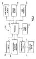
- FIG. 1a block diagram depicting an exemplary processor-based device, generally designated by the reference numeral 100 , is illustrated.
- the device 100may be any of a variety of different types, such as a computer, pager, cellular telephone, personal organizer, control circuit, etc.
- a processor 102such as a microprocessor, controls many of the functions of the device 100 .
- the device 100typically includes a power supply 104 .
- the power supply 104may include permanent batteries, replaceable batteries, and/or rechargeable batteries.
- the power supply 104may also include an A/C adapter, so that the device may be plugged into a wall outlet, for instance.
- the power supply 104may include a D/C adapter, so that the device 100 may be plugged into a vehicle's cigarette lighter.
- a user interface 106may be coupled to the processor 102 to allow a user to enter data into the device 100 .
- the user interface 106may include buttons, switches, a keyboard, a light pen, a mouse, and/or a voice recognition system.
- a display 108may also be coupled to the processor 102 to present the user with information.
- the display 108may include a liquid crystal display (LCD), a cathode ray tube (CRT), light emitting devices (LEDs), and/or an audio display.
- a radio frequency (RF) subsystem/baseband processor 110may also be coupled to the processor 102 to communicate with other devices through a wireless link.
- RFradio frequency
- the RF subsystem/baseband processor 110may include an antenna that is coupled to an RF receiver and to an RF transmitter (not shown). Also, a communication port 112 may be coupled to the processor 102 to communicate with other devices through a physical link. The communication port 112 may be adapted to be coupled to a peripheral device 114 , such as a modem, a printer, or a computer, for instance.
- a peripheral device 114such as a modem, a printer, or a computer, for instance.
- memoryis coupled to the processor 102 to store and facilitate execution of the software programs.
- the processor 102may be coupled to a memory device 116 that may be volatile memory, which may include dynamic random access memory (DRAM) and/or static random access memory (SRAM), for instance.
- DRAMdynamic random access memory
- SRAMstatic random access memory
- the amount of DRAM and SRAMmay depend on the specific design of the device 100 .
- the processor 102may also be coupled to a memory device 118 that is non-volatile memory.
- the memory device that is non-volatile memory 118may include read only memory (ROM), such as an erasable programmable ROM (EPROM), to be used in conjunction with the memory device 116 .
- ROMread only memory
- EPROMerasable programmable ROM
- the size of the ROMis typically selected to be just large enough to store any necessary operating system, application programs, and fixed data.
- the memory device 116 that is volatile memoryis typically quite large so that it can store dynamically loaded applications.
- the memory device 118 that is non-volatile memorymay include a high capacity memory, such as a disk or tape drive memory.
- the processor-based device 100may include numerous semiconductor chips in the various components that are utilized to provide the functionality to the device 100 .
- the memory device 116 that is volatile memory and the memory device 118 that is non-volatile memorymay be semiconductor chips that are coupled to the processor 102 to store the software programming for the operation of the processor-based device 100 .
- the semiconductor chipsmay exchange signals with each other and with other components of the device 100 to perform their respective functions. As such, improvements in each of the semiconductor chips may improve the efficiency of the processor-based device 100 and provide reliable access to the information stored in the memory devices 116 and 118 .
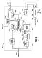
- FIG. 2a block diagram depicting an exemplary embodiment of a memory device is illustrated.
- the description of the memory device 116which may be the volatile memory device 116 of FIG. 1 , has been simplified for illustrative purposes and is not intended to be a complete description of all features in a memory device 116 .
- the present techniquemay not be limited to a memory device 116 being a specific memory type, such as SRAMs or DRAMs, but may be applicable to other devices, such as memory buses, processors, network processors, application specific integrated circuits (ASICs), and intra-chip buses, which may benefit from a local interconnect between different regions of a semiconductor chip.
- various devicesmay implement the present technique.
- the memory device 116may include a peripheral portion 201 and an array portion 203 .
- the peripheral portion 201may include various circuitry that supports the array portion 203 , such as row-address buffers 210 , row decoder 212 , column-address buffers 214 , column decoder 216 , sense amplifiers 218 , data-in circuitry 220 , data out circuitry 222 , and/or other similar circuitry.
- the array section 203may include memory structures, such as a memory array 208 that includes memory banks and cells that are used to store data.
- the memory device 116may receive various inputs that are utilized by various circuits within the memory device 116 .
- individual inputssuch as control information, address information, and data, may be provided over a memory bus to the memory device 116 .
- These individual representations of inputsare illustrated by a data bus or lines 202 , address lines 204 , and various discrete lines directed to control logic 206 .
- the memory device 116includes a memory array 208 , which comprises rows and columns of addressable memory cells. To provide access to the memory cells, each memory cell in a row is coupled to a wordline via one of the interconnects 224 , for instance. Additionally, each memory cell in a column is coupled to a bit line via one of the interconnects 226 , for instance.
- the wordline and bit linemay be utilized to access a storage capacitor through an access transistor in the memory array 208 , as can be appreciated.
- the memory device 116interfaces with, for example, a processor 102 , such as a microprocessor, through address lines 204 and data lines 202 .
- the memory device 116may interface with other devices, such as a memory controller, a microcontroller, a chip set, or another electronic system.
- the processor 102may also provide a number of control signals to the memory device 116 .
- Such control signalsmay include row and column address strobe signals RAS and CAS, a write enable signal WE, a clock enable signal CKE, and other conventional control signals.
- the control logic 206controls many available functions of the memory device 116 .
- various other control circuits and signals not detailed hereincontribute to the operation of the memory device 116 .
- Row-address buffers 210 and a row decoder 212receive and decode row addresses from row address signals provided on the address lines 204 . Each unique row address corresponds to a row of cells in the memory array 208 .
- the row-address decoder 210may also determine when a row is defective, as well as the address of a replacement row.
- the row decoder 212typically includes a wordline driver, an address decoder tree, and circuitry which translates a given row address received from the row-address buffers 210 and selectively activates the appropriate wordline of the memory array 208 via the wordline drivers.
- a column address buffer 214 and a column decoder 216receive and decode column address signals provided on the address lines 204 .
- the column decoder 216may also determine when a column is defective, as well as the address of a replacement column.
- the column decoder 216is coupled to sense amplifiers 218 via interconnects 228 .
- the sense amplifiers 218are coupled to complimentary pairs of bit lines of the memory array 208 , for example.
- the sense amplifiers 218are coupled to data-in (i.e., write) circuitry 220 via interconnections 230 and data-out (i.e., read) circuitry 222 via interconnections 232 .
- the data-in circuitry 220 and the data-out circuitry 222include data drivers and latches.
- the data bus 202provides data to the data-in circuitry 220 .
- the sense amplifier 218receives data from the data-in circuitry 220 and stores the data in the memory array 208 as a charge on a capacitor of a cell at an address specified on the address lines 204 .
- the memory device 116transfers data from the memory array 208 to the processor 102 .
- Complimentary bit lines for the accessed cellare equilibrated during a precharge operation to a reference voltage provided by an equilibration circuit and a reference voltage supply. The charge stored in the accessed cell is then shared with the associated bit line.
- the sense amplifier 218detects and amplifies a difference in voltage between the memory bit's bitline and the reference bitline. Address information received on address lines 204 is used to select a subset of the bit lines and provides them to the interconnects 232 , which may be local interconnects or buses, such as input/output (I/O) wires or lines.
- I/Oinput/output
- the amplified voltage signalsare delivered to the data-out circuitry 222 via interconnects 232 and eventually delivered to the data bus 202 .
- the data-out circuitry 222may include a data driver (not shown) to drive data out onto the data bus 202 in response to a read request directed to the memory array 208 . Further, the data-out circuitry 222 may include a data latch (not shown) to latch the read data until it is driven onto the data bus 202 by the data driver.
- signalsmay be exchanged between the peripheral portion 201 and the array portion 203 , within the components in the peripheral portion 201 and/or array portion 203 , or between the components in the peripheral portion 201 and/or array portion 203 .
- the array portion 203includes the memory array 208
- interconnects 224 and 226may provide access between the array and peripheral portions 201 and 203 .
- the array portion 203includes the memory array 208 and the sense amplifiers 218 , then interconnects 224 , 228 , 230 and 232 may provide access between the array and peripheral portions 201 and 203 .
- the interconnects 224 - 232may provide access between memory cells, such as DRAM or SRAM cells in the memory array 208 , and PMOS gates, NMOS gates, P+ active areas and N+ active areas, which may be in the peripheral portion 201 or the array portion 203 .
- the memory device 116may be designed to include a dielectric etch stop layer, such as an aluminum oxide (Al 2 O 3 ) material, a silicon carbide (SiC) material, or other suitable material, over the peripheral portion 201 and the array portion 203 of the memory device 116 , as described further below.
- a dielectric etch stop layersuch as an aluminum oxide (Al 2 O 3 ) material, a silicon carbide (SiC) material, or other suitable material, over the peripheral portion 201 and the array portion 203 of the memory device 116 , as described further below.
- the interconnects 224 - 232may be fabricated with fewer masking layers, while providing reduced resistances for high speed designs.
- the use of the dielectric etch stop layermay be included with current fabrication steps with modifications to the etching processes utilized.
- the dielectric etch stop layermay protect the peripheral portion 201 and the array portion 203 of the memory device 116 from inadvertent shorts.
- the dielectric etch stop layermay prevent any misaligned formations from causing shorts.
- the dielectric etch stop layerprovides an extra dielectric material that maintains the electrical properties of the structures, such as wordlines, buried digit lines, local interconnects, and/or active areas. Accordingly, the memory device 116 may be fabricated with fewer process steps, which may reduce the cost of fabricating the memory device 116 and improve yield.
- the exemplary techniques for fabricating a buried digit line, wordlines, bitlines, or local interconnects, such as one or more of the interconnects 224 - 232 , for example,is explained in greater detail with FIGS. 3-19 .
- FIGS. 3-19illustrate exemplary techniques for fabricating a buried digit line, wordlines, bitlines, or local interconnects within the memory device of FIG. 2 .
- the exemplary techniques described with reference to FIGS. 3-19implement a dielectric etch stop layer that may be deposited after spacer formation. This dielectric etch stop layer may be deposited over a peripheral portion 201 and an array portion 203 of the memory device 116 during fabrication, for instance. Accordingly, the dielectric etch stop layer may reduce shorts within the memory device 116 from coupling the interconnects 224 - 232 or local interconnects to the various components, which may provide access to wordlines, gates, and active areas in the peripheral and array portions 201 and 203 of the memory device 116 . As will be evident from the description below, the various alternatives to the process described with respect to the FIGS. 3-19 may be implemented.
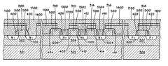
- FIG. 3illustrates a cross-sectional view of a portion of a memory device 116 of FIG. 2 to illustrate an exemplary method of fabricating the BDL/LI layer.
- a substrate 300may include different portions of a silicon wafer implemented to fabricate the memory device 116 .
- the substrate 300may be divided into a first peripheral section 301 , an array section 302 , and a second peripheral section 304 .
- the first peripheral section 301may be an N channel peripheral section of the substrate 300 with a P well 305
- the array section 302may be an N channel array section of the substrate 300 with a P well 306
- the second peripheral section 304may be a P channel peripheral section of the substrate 300 with an N well 307 .
- the sections 301 - 304may also include a number of layers disposed thereon such that the processing described herein occurs over any number of layers already deposited on the wafer, as can be appreciated by those skilled in the art.
- a NMOS gate 308Deposited over the sections 301 - 304 , a NMOS gate 308 , wordlines 310 - 316 , and a PMOS gate 318 may be formed, which may be a portion of interconnects 224 - 232 of FIG. 2 .
- the NMOS gate 308 , wordlines 310 - 316 , and the PMOS gate 318may comprise a plurality of layers, which form a wordline stack.
- the wordline stackmay include a doped semiconductor layer, such as a polysilicon layer, a first conductive layer, such as a tungsten nitride (WN x ) layer, a second conductive layer, such as a tungsten (W) layer, and a cap layer, such as a silicon nitride layer.
- a doped semiconductor layersuch as a polysilicon layer
- a first conductive layersuch as a tungsten nitride (WN x ) layer
- a second conductive layersuch as a tungsten (W) layer
- a cap layersuch as a silicon nitride layer.
- Each of the NMOS gate 308 , wordlines 310 - 316 , and the PMOS gate 318may be formed on a gate oxide layer that is a portion of the substrate 300 or formed over the substrate and below the NMOS gate 308 , wordlines 310 - 316 , and the PMOS gate 318 .
- NMOS gate 308various insulating materials, such as oxides, silicon nitride, or other such dielectric materials may be deposited.
- a doped regionmay be formed between the wordlines 310 - 316 in or over the sections 301 - 304 .
- the NMOS gate 308 , wordlines 310 - 316 , and the PMOS gate 318may be formed through chemical vapor deposition, physical vapor deposition, or other similar processes that form a thin film of material on the surface of a substrate 300 or structures.
- the techniques for forming the w NMOS gate 308 , wordlines 310 - 316 , and the PMOS gate 318 and related structureswill be appreciated by those skilled in the art.
- spacers 400 - 422may be formed adjacent to the NMOS gate 308 , wordlines 310 - 316 , and the PMOS gate 318 .
- the spacers 400 - 422may be formed by depositing a dielectric layer and etching the dielectric layer from a portion of the sections 301 - 304 and a portion of the NMOS gate 308 , wordlines 310 - 316 , and the PMOS gate 318 .
- the spacers 400 - 422may be utilized to provide insulation from neighboring regions, to protect the NMOS gate 308 , wordlines 310 - 316 , and the PMOS gate 318 from damage during the various fabrication steps and to provide implant boundaries for defining transistor characteristics.
- the spacers 400 - 422may be formed from a dielectric material, such as an oxide or nitride material, or other suitable material that may provide sidewall insulation for the NMOS gate 308 , wordlines 310 - 316 , and the PMOS gate 318 . Further, the spacers 400 - 422 may be designed to a specific thickness to provide self-aligned contacts in later fabrication steps, as discussed below. The technique for forming the spacers 400 - 422 will be appreciated by those skilled in the art.
- a dielectric etch stop layer 500may be deposited over the sections 301 - 304 , including the wordlines 308 - 318 and spacers 400 - 422 , as shown in FIG. 5 .
- the dielectric etch stop layer 500may be selected to prevent the etching or removal of an underlying nitride or oxide material.
- selectivityrefers to the relative etch rate of different materials. For instance, the selectivity may relate to the etching of the overlying material at a faster rate than the underlying material. The selectivity is generally expressed as a ratio of the etch rate of the underlying material verses the etch rate of the overlying material.
- the dielectric etch stop layer 500may be a material that may stop or slow the etching of a material over the dielectric etch stop layer 500 to prevent damage or over etching.
- the dielectric etch stop layer 500may be an aluminum oxide Al 2 O 3 , a silicon carbide SiC, hafnium oxide HfO 2 , hafnium aluminum oxide HfAlO, silicon carbon nitride SiCN, silicon nitride Si 3 N 4 , silicon oxide SiO 2 , yttrium oxide YO 2 , or tantalum pentoxide Ta 2 O 5 .
- the use of the dielectric etch stop layer 500will be discussed further with reference to FIGS. 11-19 .
- a photoresist 600may be deposited over the sections 301 - 304 , the NMOS gate 308 , wordlines 310 - 316 , the PMOS gate 318 , and spacers 400 - 422 , and subsequently developed to expose portions of the dielectric etch stop layer 500 , which may also be etched to expose the first peripheral section 301 , the NMOS gate 308 , and the spacers 400 and 402 .
- the photoresist 600may utilize photolithographic processes to form the structure illustrated in FIG. 6 .
- the photoresist 600may be a light sensitive material that changes its properties when exposed to light.
- photoresistmay be a liquid chemical that is spun or rolled onto the sections 301 - 304 .
- the photoresist 600may be developed by exposure to an ultraviolet light or light of a specific frequency, which is utilized to form a pattern in the photoresist 600 .
- an etchantmay be utilized to remove selected portions of the photoresist 600 according to the exposed pattern to form a desired pattern in the photoresist 600 .
- another etchantwhich may be part of a dry and/or wet etching process, may be utilized to remove the exposed portions of the dielectric etch stop layer 500 .
- the etchant used in the etching processmay remove the dielectric etch stop layer 500 to expose the first peripheral section 301 , the NMOS gate 308 and the spacers 400 and 402 , as illustrated in FIG. 6 . It should be understood that those in the art readily understand the deposition, development, and etching techniques used to construct the pattern in the photoresist 600 .
- the active areas or doped regions 700 and 702may be formed adjacent to the NMOS gate 308 through conventional techniques. These techniques may include diffusion, ion implantation, or other similar process for introducing dopants into the first peripheral section 301 . Dopants are generally selected from group V on the periodic chart, which may include Phosphorus (P), Antimony (Sb), and/or Arsenic (As), for example. As a result of the doping process, the N+ doped regions 700 and 702 may be formed in the N channel silicon of the first peripheral section 301 .
- the photoresist 600may be removed by a wet etch and/or a dry strip process, such as a chemical rinse, for example, and another photoresist 800 may be deposited over the sections 301 - 304 including the NMOS gate 308 , wordlines 310 316 , the PMOS gate 318 and spacers 400 - 422 , and subsequently developed to expose portions of the dielectric etch stop layer 500 , which may be etched to expose the second peripheral section 304 for another doping process. As shown in FIG. 8 , a photoresist 800 may be applied to the second peripheral section 304 to form a pattern in the photoresist 800 .
- a photoresist 800may be applied to the second peripheral section 304 to form a pattern in the photoresist 800 .
- the photoresist 800may be developed to expose portions of the dielectric etch stop layer 500 for another etching process to expose the second peripheral section 304 , the PMOS gate 318 , and the spacers 420 and 422 . As noted above with regard to the description of FIG. 6 , it should be understood that those in the art readily understand the deposition, development, and etching techniques used to construct the pattern in the photoresist 800 .
- the second peripheral section 304 , the PMOS gate 318 and spacers 420 and 422may be exposed to a P+ doping process, as shown in FIG. 9 .
- the P+ doping processmay form active areas or doped regions 900 and 902 .
- the P+ dopantsmay include Boron (B), Aluminum (Al), Indium (In) or Gallium (Ga), for example.
- the P+ doped regions 900 and 902may be formed in the second peripheral section 304 adjacent to the PMOS gate 318 .
- the photoresist 800may be removed, as shown in FIG. 10 .
- an etchant that is selective to the photoresist 800 relative to the dielectric etch stop layer 500may be utilized to remove the photoresist 800 from the sections 301 - 304 , the NMOS gate 308 , wordlines 310 - 316 , the PMOS gate 318 , spacers 400 - 422 and the dielectric etch stop layer 500 .
- the etchantmay remove the photoresist 800 , but leaves the dielectric etch stop layer 500 over the array section 302 , wordlines 310 - 316 , and the spacers 404 - 418 .
- a first dielectric layer 1100may be deposited and patterned over the sections 301 - 304 , the NMOS gate 308 , wordlines 310 - 316 , the PMOS gate 318 , spacers 400 - 422 , and the dielectric etch stop layer 500 using conventional techniques. These conventional techniques may include chemical vapor deposition, physical vapor deposition, sputtering, atomic layer deposition, or any other suitable deposition process.
- the first dielectric layer 1100may include material, such as an oxide, a nitride, a glass, such as Boro-Phospho-Silicate Glass (BPSG), or any other suitable material having dielectric properties.
- BPSGBoro-Phospho-Silicate Glass
- the first dielectric layer 1100is different from the dielectric etch stop layer 500 to allow selective etching in relation to the dielectric etch stop layer 500 .
- the dielectric layer 1100may be planarized over the sections 301 - 304 , the NMOS gate 308 , wordlines 310 - 316 , the PMOS gate 318 , spacers 400 - 422 , and the dielectric etch stop layer 500 using conventional techniques.
- the NMOS gate 308 , wordlines 310 - 316 , the PMOS gate 318 or the dielectric etch stop layer 500 over the NMOS gate 308 , wordlines 310 - 316 , and the PMOS gate 318may be exposed.
- the dielectric etch stop layer 500 and the first dielectric layer 1100may be patterned and etched between the wordlines 310 - 316 to provide access to the array section 302 , which may include active areas or doped regions 1200 - 1204 in the array section 302 .
- the etching of the dielectric etch stop layer 500 and the dielectric layer 1100may expose the array section 302 through openings 1206 - 1210 that are between the wordlines 310 - 316 .
- the openings 1206 - 1210may be utilized to provide self-aligned contact formations that provide access to the array section 302 .
- a doping processsuch as a N+doping process, may be utilized to dope the regions 1200 - 1204 . It should be noted that the doped regions 1200 - 1204 may be doped before and/or after the dielectric etch stop layer 500 is removed.
- conductive plugs 1300 - 1304may be deposited within the openings 1206 - 1210 .
- the conductive plugs 1300 - 1304may comprise an amorphous, partially, or totally poly crystalline form of silicon, N-doped or P-doped polysilicon, titanium (Ti), titanium nitride (TiN), tungsten (W), an epitaxially grown silicon, or any other suitable conductive material.
- the conductive plugs 1300 - 1304may be created from a chemical vapor deposition process that utilizes a silicon gas, such as silane (SiH 4 ).
- the conductive plugs 1300 - 1304may be deposited over the array section 302 and between the spacers 406 - 408 , 410 - 412 , and 414 - 416 .
- a second dielectric layer 1400may be deposited and patterned over the sections 301 - 304 , the NMOS gate 308 , wordlines 310 - 316 , the PMOS gate 318 , spacers 400 - 422 , the dielectric etch stop layer 500 , first dielectric layer 1100 and conductive plugs 1300 - 1304 using conventional techniques. These conventional techniques may include chemical vapor deposition, physical vapor deposition, sputtering, atomic layer deposition, or other suitable deposition process.
- the second dielectric layer 1400may include a material, such as a tetraethyl-orthosilicate (TEOS), a nitride material, or any other dielectric material.
- TEOStetraethyl-orthosilicate
- the second dielectric layer 1400is different from the dielectric etch stop layer 500 to allow selective etching in relation to the dielectric etch stop layer 500 .
- the second dielectric layer 1400may be applied directly over the NMOS gate 308 , wordlines 310 - 316 , the PMOS gate 318 or the dielectric etch stop layer 500 .
- an etchantmay be utilized to create various openings 1500 - 1506 within the first dielectric layer 1100 and the second dielectric layer 1400 .
- a dry etching and/or wet etching processmay be utilized. The process may use an etchant that may penetrate the first dielectric layer 1100 and the second dielectric layer 1400 .
- the openings 1500 - 1506may expose various regions of the substrate 300 , such as doped regions 702 and 900 and the conductive plugs 1300 and 1304 .
- the opening 1500exposes the doped region 702 , which is an N+ active area on the first peripheral section 301
- the opening 1506exposes the doped region 900 , which is a P+ active area in the second peripheral section 304 .
- the openings 1502 and 1504may provide access to the conductive plugs 1300 and 1304 .
- the exposure of the wordline 310 - 316may create shorts or otherwise damage the memory device 116 .
- the etching patternmay be misaligned and expose a portion of the wordline 310 .
- the etchantmay be selective to the first dielectric layer 1100 and the second dielectric layer 1400 relative to the dielectric etch stop layer 500 .
- the wordline 310may remain protected by the dielectric etch stop layer 500 to prevent inadvertent exposure by the etching process.
- the dielectric etch stop layer 500may prevent the etching process that formed the openings 1500 - 1506 from exposing the wordlines 310 - 316 , which may cause shorts in later processes.
- the dielectric etch stop layer 500may prevent the etching process that formed the openings 1500 - 1506 from exposing the wordlines 310 - 316 , because the etching of the openings 1500 and 1506 may require a longer etching period to reach the doped regions 702 or 900 .
- the openings 1500 and 1506may extend to the doped regions 702 and 900 , which are a portion of or formed on the sections 301 and 304 .
- the openings 1502 and 1504may be to the conductive plugs 1300 and 1304 , which are formed above the array section 302 .
- the dielectric etch stop layer 500may prevent over etching in the areas adjacent to the conductive plugs 1300 and 1304 .
- the wordlines 310 - 316may remain protected by the dielectric etch stop layer 500 to prevent inadvertent exposure from over etching.
- openings 1502 , 1504 , 1600 and 1602may also be created within the first dielectric layer 1100 and the second dielectric layer 1400 .
- the openings 1502 , 1504 , 1600 and 1602may expose various regions of the substrate 300 , such as the NMOS gate 308 , the PMOS gate 318 , and the wordlines 310 and 314 .
- the openings 1502 and 1504exposes the conductive plugs 1300 and 1304 that are part of the section 302 .
- the openings 1600 and 1602may provide access to the NMOS gate 308 and PMOS gate 318 , respectively.
- the etch patternmay be misaligned and etch into the first dielectric layer 1100 or the second dielectric layer 1400 adjacent to the wordlines 310 - 316 .
- the dielectric etch stop layer 500may protect portions of the array section 302 or the wordlines 310 - 316 from being exposed by the etching process that creates the openings 1600 and 1602 .
- a buried digit line or local interconnect (BDL/LI) layer 1700may be deposited in the openings 1500 - 1506 and over the second dielectric layer 1400 .
- the BDL/LI layer 1700may provide access to the doped regions 1200 - 1204 between the wordlines 310 and 316 and/or to the conductive plugs 1300 and 1304 of the array section 302 and the doped regions 702 and 900 of the peripheral sections 301 and 304 .
- This interconnectionprovides access between memory cells formed on the array section 302 along with active areas and gates on the peripheral sections 301 and 304 .
- the BDL/LI layer 1700may include a conductive material, such as polysilicon, tungsten (W), copper (Cu), or other similar conductive materials. Further, the BDL/LI layer 1700 may be selected to provide ohmic connection to various materials, such as the conductive plugs 1300 and 1304 , doped regions 702 and 900 , and/or the NMOS gate 308 and the PMOS gate 318 , respectively.
- the dielectric etch stop layer 500may protect areas that are inadvertently exposed during the etching processes.
- the etching of the openings 1500 - 1506 and 1600 - 1602may vary in the depth in some of the regions, the dielectric etch stop layer 500 may prevent the etchant from exposing other regions, which may again cause shorts. Accordingly, the dielectric etch stop layer 500 may prevent shorts between the BDL/LI layer 1700 , the wordlines 310 - 316 , and the conductive plugs 1300 - 1304 .
- the dielectric etch stop layer 500may be formed with the addition of a dielectric etch stop deposition process, and two dielectric etch stop etching processes.
- the dielectric etch stop layer 500may be formed as part of the NMOS gate 308 , wordlines 310 - 316 , and/or the PMOS gate 318 .
- the later etching processesmay not have to be modified to penetrate the dielectric etch stop layer 500 in the array section 302 .
- the NMOS gate 308 , wordlines 310 - 316 , and the PMOS gate 318may comprise a plurality of layers, such as a doped semiconductor layer, a first conductive layer, a second conductive layer, a cap layer, and a dielectric etch stop layer 500 .
- the etchant utilized to form the spacers 400 - 422may be selective to the material utilized for the spacers 400 - 422 relative to the material in the dielectric etch stop layer 500 .
- the dielectric etch stop layer 500may be formed as part of the NMOS gate 308 , wordlines 310 - 316 , and the PMOS gate 318 and provide protection to the wordline stack through the processing of the different structures.
- the dielectric etch stop layer 500may be deposited before the spacers 400 - 422 are formed.
- the spacers 400 - 422may be formed over the dielectric etch stop layer 500 on either side of the NMOS gate 308 , wordlines 310 - 316 , and the PMOS gate 318 .
- the etchant utilized to form the spacers 400 - 422may be selective to the material utilized for the spacers 400 - 422 relative to the material in the dielectric etch stop layer 500 .
- the various fabrication stepsmay be altered or performed in a different order.
- the doping of the N+ doped regions 700 and 702 and/or P+ doped regions 900 and 902may be performed before and/or after the removal of the dielectric etch stop layer 500 from the peripheral sections 301 and 304 .
- the photoresist 600 and/or 800may be removed in the same etching process along with the dielectric etch stop layer 500 . Accordingly, it should be appreciated that the fabrication steps may be altered.
Landscapes
- Engineering & Computer Science (AREA)
- Manufacturing & Machinery (AREA)
- Physics & Mathematics (AREA)
- Condensed Matter Physics & Semiconductors (AREA)
- General Physics & Mathematics (AREA)
- Computer Hardware Design (AREA)
- Microelectronics & Electronic Packaging (AREA)
- Power Engineering (AREA)
- Semiconductor Memories (AREA)
- Internal Circuitry In Semiconductor Integrated Circuit Devices (AREA)
Abstract
Description
- This application is a continuation of application Ser. No. 10/832,688, which was filed on Apr. 27, 2004.
- 1. Field of the Invention
- The present invention relates generally to semiconductor devices and, more particularly, to the fabrication of a buried digit line in a memory device.
- 2. Description of the Related Art
- This section is intended to introduce the reader to various aspects of art which may be related to various aspects of the present invention which are described and/or claimed below. This discussion is believed to be helpful in providing the reader with background information to facilitate a better understanding of the various aspects of the present invention. Accordingly, it should be understood that these statements are to be read in this light, and not as admissions of prior art.
- Microprocessor-controlled integrated circuits are used in a wide variety of applications. Such applications include personal computers, telephones, portable devices, networks, and a host of other consumer products. As is well known, microprocessors are essentially generic devices that perform specific functions under the control of a software program. This software program is stored in a memory device that is coupled to the microprocessor. Not only does the microprocessor access the memory devices to retrieve the software program instruction, but it also facilitates storage and retrieval of data created during the execution of the program in one or more of the memory devices.
- It should be understood that the memory devices are typically mass produced through fabrication processes to form various structures in a semiconductor chip. In forming the structures, different materials are layered together to form signal paths or circuitry that are utilized by the memory device. These structures are connected together to facilitate the exchange signals and distribute power throughout the semiconductor chip. Additionally, the structures within the semiconductor chip may be divided into different sections, such as an array section and a peripheral section. The array section may include memory structures, such as memory cells and banks that are used to store data, while the peripheral section may include larger structures that support the array, such as drivers, decoders and/or other similar circuitry.
- Regardless of the specific structures being fabricated, it is often desirable to minimize the size of the structures to allow for greater density and to reduce the contact resistance between different structures within the semiconductor chip. Generally, the critical dimensions of the structures patterned on the semiconductor chips are becoming increasingly complex as the structures are designed to operate at higher speeds. As these critical dimensions change, the electrical properties of the structures and integrated circuits vary in relation to the critical dimensions. Therefore, it is important to maintain the critical dimensions to achieve consistency in the electrical properties of the structures.
- For instance, in stack capacitor dynamic random access memory (DRAM) cells, cell height may continue to increase, while the contact size is minimized. As a result, the contact resistance in the peripheral circuitry may increase, which makes high-speed designs for structures increasingly challenging. To reduce the contact resistances for the connections between the array section and the peripheral section of a memory device, a buried digit line (BDL) layer may also be utilized as a local interconnect (LI), which is a short interconnect between structures, or as a bus, which is a longer interconnect between structures. The buried digit line or local interconnect (BDL/LI) layer may have connections to different structures, such as dynamic random access memory (DRAM) cells, p-type metal oxide semiconductor (PMOS) gates, n-type metal oxide semiconductor (NMOS) gates, P+ active areas and N+ active areas, which are formed in the peripheral and array sections of the semiconductor chip.
- In fabricating the BDL/LI layer, two to three masking layers are generally utilized in the fabrication process to provide access from the BDL/LI layer to different areas of the device. These additional masking layers consume valuable fabrication time and increase the cost of manufacturing the semiconductor chip. Accordingly, minimizing the masking layers and corresponding deposition/etch steps may enhance the fabrication process of the semiconductor chip.
- The foregoing and other advantages of the invention may become apparent upon reading the following detailed description and upon reference to the drawings in which:
FIG. 1 illustrates a block diagram of an exemplary processor-based device that incorporates the present technique;FIG. 2 illustrates a block diagram depicting an exemplary embodiment of a memory device utilized in the processor-based device ofFIG. 1 ; andFIGS. 3-19 illustrate cross-sectional views of portions of the memory device ofFIG. 2 during different stages of fabrication.- One or more specific embodiments of the present invention will be described below. In an effort to provide a concise description of these embodiments, not all features of an actual implementation may be described in the specification. It should be appreciated that in the development of any such actual implementation, as in any engineering or design project, numerous implementation-specific decisions are made to achieve the developers' specific goals, such as compliance with system-related and business-related constraints, which may vary from one implementation to another. Moreover, it should be appreciated that such a development effort might be complex and time consuming, but would nevertheless be a routine undertaking of design, fabrication, and manufacture for those of ordinary skill having the benefit of this disclosure.
- The present technique is an improved approach for fabricating a buried digit line, wordlines, or bitlines, which may also be used as a local interconnect or a bus. In accordance with the present technique, a dielectric etch stop layer may be utilized to enable access between the peripheral and array sections of a memory device. The dielectric etch stop layer may provide protection from over etching and misaligned pattern etching that may cause shorts within the memory device, thereby increasing processing yield. In addition, the dielectric etch stop layer may reduce the masking steps that are utilized to form the BDL/LI layer within the memory device, which may reduce the processing time and cost of fabricating the memory device.
- Turning now to the drawings, and referring initially to
FIG. 1 , a block diagram depicting an exemplary processor-based device, generally designated by thereference numeral 100, is illustrated. Thedevice 100 may be any of a variety of different types, such as a computer, pager, cellular telephone, personal organizer, control circuit, etc. In a typical processor-based device, aprocessor 102, such as a microprocessor, controls many of the functions of thedevice 100. - The
device 100 typically includes apower supply 104. For instance, if thedevice 100 is portable, thepower supply 104 may include permanent batteries, replaceable batteries, and/or rechargeable batteries. Thepower supply 104 may also include an A/C adapter, so that the device may be plugged into a wall outlet, for instance. In addition, thepower supply 104 may include a D/C adapter, so that thedevice 100 may be plugged into a vehicle's cigarette lighter. - Various other components may also be coupled to the
processor 102, which may depend on the functions that thedevice 100 performs. For instance, auser interface 106 may be coupled to theprocessor 102 to allow a user to enter data into thedevice 100. Theuser interface 106 may include buttons, switches, a keyboard, a light pen, a mouse, and/or a voice recognition system. Adisplay 108 may also be coupled to theprocessor 102 to present the user with information. Thedisplay 108 may include a liquid crystal display (LCD), a cathode ray tube (CRT), light emitting devices (LEDs), and/or an audio display. Furthermore, a radio frequency (RF) subsystem/baseband processor 110 may also be coupled to theprocessor 102 to communicate with other devices through a wireless link. The RF subsystem/baseband processor 110 may include an antenna that is coupled to an RF receiver and to an RF transmitter (not shown). Also, acommunication port 112 may be coupled to theprocessor 102 to communicate with other devices through a physical link. Thecommunication port 112 may be adapted to be coupled to aperipheral device 114, such as a modem, a printer, or a computer, for instance. - Because the
processor 102 controls the functioning of thedevice 100, which is generally under the control of software programming, memory is coupled to theprocessor 102 to store and facilitate execution of the software programs. For instance, theprocessor 102 may be coupled to amemory device 116 that may be volatile memory, which may include dynamic random access memory (DRAM) and/or static random access memory (SRAM), for instance. The amount of DRAM and SRAM may depend on the specific design of thedevice 100. Theprocessor 102 may also be coupled to amemory device 118 that is non-volatile memory. The memory device that isnon-volatile memory 118 may include read only memory (ROM), such as an erasable programmable ROM (EPROM), to be used in conjunction with thememory device 116. The size of the ROM is typically selected to be just large enough to store any necessary operating system, application programs, and fixed data. Thememory device 116 that is volatile memory, on the other hand, is typically quite large so that it can store dynamically loaded applications. Additionally, thememory device 118 that is non-volatile memory may include a high capacity memory, such as a disk or tape drive memory. - The processor-based
device 100 may include numerous semiconductor chips in the various components that are utilized to provide the functionality to thedevice 100. For instance, thememory device 116 that is volatile memory and thememory device 118 that is non-volatile memory may be semiconductor chips that are coupled to theprocessor 102 to store the software programming for the operation of the processor-baseddevice 100. The semiconductor chips may exchange signals with each other and with other components of thedevice 100 to perform their respective functions. As such, improvements in each of the semiconductor chips may improve the efficiency of the processor-baseddevice 100 and provide reliable access to the information stored in thememory devices - Turning now to
FIG. 2 , a block diagram depicting an exemplary embodiment of a memory device is illustrated. The description of thememory device 116, which may be thevolatile memory device 116 ofFIG. 1 , has been simplified for illustrative purposes and is not intended to be a complete description of all features in amemory device 116. Likewise, the present technique may not be limited to amemory device 116 being a specific memory type, such as SRAMs or DRAMs, but may be applicable to other devices, such as memory buses, processors, network processors, application specific integrated circuits (ASICs), and intra-chip buses, which may benefit from a local interconnect between different regions of a semiconductor chip. As such, various devices may implement the present technique. - The
memory device 116 may include aperipheral portion 201 and anarray portion 203. Theperipheral portion 201 may include various circuitry that supports thearray portion 203, such as row-address buffers 210,row decoder 212, column-address buffers 214,column decoder 216,sense amplifiers 218, data-incircuitry 220, data outcircuitry 222, and/or other similar circuitry. Thearray section 203 may include memory structures, such as amemory array 208 that includes memory banks and cells that are used to store data. - During operation, the
memory device 116 may receive various inputs that are utilized by various circuits within thememory device 116. For instance, individual inputs, such as control information, address information, and data, may be provided over a memory bus to thememory device 116. These individual representations of inputs are illustrated by a data bus orlines 202,address lines 204, and various discrete lines directed to controllogic 206. Thememory device 116 includes amemory array 208, which comprises rows and columns of addressable memory cells. To provide access to the memory cells, each memory cell in a row is coupled to a wordline via one of theinterconnects 224, for instance. Additionally, each memory cell in a column is coupled to a bit line via one of theinterconnects 226, for instance. The wordline and bit line may be utilized to access a storage capacitor through an access transistor in thememory array 208, as can be appreciated. - The
memory device 116 interfaces with, for example, aprocessor 102, such as a microprocessor, throughaddress lines 204 anddata lines 202. Alternatively, thememory device 116 may interface with other devices, such as a memory controller, a microcontroller, a chip set, or another electronic system. Theprocessor 102 may also provide a number of control signals to thememory device 116. Such control signals may include row and column address strobe signals RAS and CAS, a write enable signal WE, a clock enable signal CKE, and other conventional control signals. Thecontrol logic 206 controls many available functions of thememory device 116. In addition, various other control circuits and signals not detailed herein contribute to the operation of thememory device 116. - Row-
address buffers 210 and arow decoder 212 receive and decode row addresses from row address signals provided on the address lines204. Each unique row address corresponds to a row of cells in thememory array 208. The row-address decoder 210 may also determine when a row is defective, as well as the address of a replacement row. Therow decoder 212 typically includes a wordline driver, an address decoder tree, and circuitry which translates a given row address received from the row-address buffers 210 and selectively activates the appropriate wordline of thememory array 208 via the wordline drivers. - A
column address buffer 214 and acolumn decoder 216 receive and decode column address signals provided on the address lines204. Thecolumn decoder 216 may also determine when a column is defective, as well as the address of a replacement column. Thecolumn decoder 216 is coupled to senseamplifiers 218 viainterconnects 228. Thesense amplifiers 218 are coupled to complimentary pairs of bit lines of thememory array 208, for example. - The
sense amplifiers 218 are coupled to data-in (i.e., write)circuitry 220 viainterconnections 230 and data-out (i.e., read)circuitry 222 viainterconnections 232. The data-incircuitry 220 and the data-outcircuitry 222 include data drivers and latches. During a write operation, thedata bus 202 provides data to the data-incircuitry 220. Thesense amplifier 218 receives data from the data-incircuitry 220 and stores the data in thememory array 208 as a charge on a capacitor of a cell at an address specified on the address lines204. - During a read operation, the
memory device 116 transfers data from thememory array 208 to theprocessor 102. Complimentary bit lines for the accessed cell are equilibrated during a precharge operation to a reference voltage provided by an equilibration circuit and a reference voltage supply. The charge stored in the accessed cell is then shared with the associated bit line. Thesense amplifier 218 detects and amplifies a difference in voltage between the memory bit's bitline and the reference bitline. Address information received onaddress lines 204 is used to select a subset of the bit lines and provides them to theinterconnects 232, which may be local interconnects or buses, such as input/output (I/O) wires or lines. The amplified voltage signals are delivered to the data-outcircuitry 222 viainterconnects 232 and eventually delivered to thedata bus 202. The data-outcircuitry 222 may include a data driver (not shown) to drive data out onto thedata bus 202 in response to a read request directed to thememory array 208. Further, the data-outcircuitry 222 may include a data latch (not shown) to latch the read data until it is driven onto thedata bus 202 by the data driver. - During operation of the
memory device 116, signals may be exchanged between theperipheral portion 201 and thearray portion 203, within the components in theperipheral portion 201 and/orarray portion 203, or between the components in theperipheral portion 201 and/orarray portion 203. For instance, if thearray portion 203 includes thememory array 208,interconnects peripheral portions array portion 203 includes thememory array 208 and thesense amplifiers 218, then interconnects224,228,230 and232 may provide access between the array andperipheral portions memory array 208, and PMOS gates, NMOS gates, P+ active areas and N+ active areas, which may be in theperipheral portion 201 or thearray portion 203. - In fabricating these interconnects224-232, which may be referred to as buried digit lines, wordlines, or bitlines, different fabrication processes and steps may be utilized to form the interconnection between the various structures, which may be buses and/or local interconnects. Accordingly, it may be advantageous to reduce the number of masking layers utilized to form the interconnects224-232. For instance, the
memory device 116 may be designed to include a dielectric etch stop layer, such as an aluminum oxide (Al2O3) material, a silicon carbide (SiC) material, or other suitable material, over theperipheral portion 201 and thearray portion 203 of thememory device 116, as described further below. By utilizing the dielectric etch stop layer, the interconnects224-232 may be fabricated with fewer masking layers, while providing reduced resistances for high speed designs. The use of the dielectric etch stop layer may be included with current fabrication steps with modifications to the etching processes utilized. - In addition, the dielectric etch stop layer may protect the
peripheral portion 201 and thearray portion 203 of thememory device 116 from inadvertent shorts. The dielectric etch stop layer may prevent any misaligned formations from causing shorts. With the reduction in the dimensions of the structures and the increase in cell height, the dielectric etch stop layer provides an extra dielectric material that maintains the electrical properties of the structures, such as wordlines, buried digit lines, local interconnects, and/or active areas. Accordingly, thememory device 116 may be fabricated with fewer process steps, which may reduce the cost of fabricating thememory device 116 and improve yield. The exemplary techniques for fabricating a buried digit line, wordlines, bitlines, or local interconnects, such as one or more of the interconnects224-232, for example, is explained in greater detail withFIGS. 3-19 . FIGS. 3-19 illustrate exemplary techniques for fabricating a buried digit line, wordlines, bitlines, or local interconnects within the memory device ofFIG. 2 . The exemplary techniques described with reference toFIGS. 3-19 implement a dielectric etch stop layer that may be deposited after spacer formation. This dielectric etch stop layer may be deposited over aperipheral portion 201 and anarray portion 203 of thememory device 116 during fabrication, for instance. Accordingly, the dielectric etch stop layer may reduce shorts within thememory device 116 from coupling the interconnects224-232 or local interconnects to the various components, which may provide access to wordlines, gates, and active areas in the peripheral andarray portions memory device 116. As will be evident from the description below, the various alternatives to the process described with respect to theFIGS. 3-19 may be implemented.- Turning now to the first exemplary process for fabricating a buried digit line, wordlines, or bitlines, which may be utilized as a local interconnect in accordance with the present techniques,
FIG. 3 illustrates a cross-sectional view of a portion of amemory device 116 ofFIG. 2 to illustrate an exemplary method of fabricating the BDL/LI layer. In one exemplary embodiment, asubstrate 300 may include different portions of a silicon wafer implemented to fabricate thememory device 116. Thesubstrate 300 may be divided into a firstperipheral section 301, anarray section 302, and a secondperipheral section 304. The firstperipheral section 301 may be an N channel peripheral section of thesubstrate 300 with a P well305, while thearray section 302 may be an N channel array section of thesubstrate 300 with aP well 306. The secondperipheral section 304 may be a P channel peripheral section of thesubstrate 300 with an N well307. The sections301-304 may also include a number of layers disposed thereon such that the processing described herein occurs over any number of layers already deposited on the wafer, as can be appreciated by those skilled in the art. - Deposited over the sections301-304, a
NMOS gate 308, wordlines310-316, and aPMOS gate 318 may be formed, which may be a portion of interconnects224-232 ofFIG. 2 . TheNMOS gate 308, wordlines310-316, and thePMOS gate 318 may comprise a plurality of layers, which form a wordline stack. For instance, the wordline stack may include a doped semiconductor layer, such as a polysilicon layer, a first conductive layer, such as a tungsten nitride (WNx) layer, a second conductive layer, such as a tungsten (W) layer, and a cap layer, such as a silicon nitride layer. Each of theNMOS gate 308, wordlines310-316, and thePMOS gate 318 may be formed on a gate oxide layer that is a portion of thesubstrate 300 or formed over the substrate and below theNMOS gate 308, wordlines310-316, and thePMOS gate 318. Further, between each of theNMOS gate 308, wordlines310-316, and thePMOS gate 318 various insulating materials, such as oxides, silicon nitride, or other such dielectric materials may be deposited. In addition, a doped region may be formed between the wordlines310-316 in or over the sections301-304. TheNMOS gate 308, wordlines310-316, and thePMOS gate 318 may be formed through chemical vapor deposition, physical vapor deposition, or other similar processes that form a thin film of material on the surface of asubstrate 300 or structures. The techniques for forming thew NMOS gate 308, wordlines310-316, and thePMOS gate 318 and related structures will be appreciated by those skilled in the art. - As shown in
FIG. 4 , spacers400-422 may be formed adjacent to theNMOS gate 308, wordlines310-316, and thePMOS gate 318. The spacers400-422 may be formed by depositing a dielectric layer and etching the dielectric layer from a portion of the sections301-304 and a portion of theNMOS gate 308, wordlines310-316, and thePMOS gate 318. The spacers400-422 may be utilized to provide insulation from neighboring regions, to protect theNMOS gate 308, wordlines310-316, and thePMOS gate 318 from damage during the various fabrication steps and to provide implant boundaries for defining transistor characteristics. The spacers400-422 may be formed from a dielectric material, such as an oxide or nitride material, or other suitable material that may provide sidewall insulation for theNMOS gate 308, wordlines310-316, and thePMOS gate 318. Further, the spacers400-422 may be designed to a specific thickness to provide self-aligned contacts in later fabrication steps, as discussed below. The technique for forming the spacers400-422 will be appreciated by those skilled in the art. - After spacer formation, a dielectric
etch stop layer 500 may be deposited over the sections301-304, including the wordlines308-318 and spacers400-422, as shown inFIG. 5 . The dielectricetch stop layer 500 may be selected to prevent the etching or removal of an underlying nitride or oxide material. Generally, selectivity refers to the relative etch rate of different materials. For instance, the selectivity may relate to the etching of the overlying material at a faster rate than the underlying material. The selectivity is generally expressed as a ratio of the etch rate of the underlying material verses the etch rate of the overlying material. Because the dielectricetch stop layer 500 is chosen to prevent the etching of the spacers400-422 and/or the nitride layer of theNMOS gate 308, wordlines310-316, and thePMOS gate 318, the dielectricetch stop layer 500 may be a material that may stop or slow the etching of a material over the dielectricetch stop layer 500 to prevent damage or over etching. Accordingly, the dielectricetch stop layer 500 may be an aluminum oxide Al2O3, a silicon carbide SiC, hafnium oxide HfO2, hafnium aluminum oxide HfAlO, silicon carbon nitride SiCN, silicon nitride Si3N4, silicon oxide SiO2, yttrium oxide YO2, or tantalum pentoxide Ta2O5. The use of the dielectricetch stop layer 500 will be discussed further with reference toFIGS. 11-19 . - Referring now to
FIG. 6 , aphotoresist 600 may be deposited over the sections301-304, theNMOS gate 308, wordlines310-316, thePMOS gate 318, and spacers400-422, and subsequently developed to expose portions of the dielectricetch stop layer 500, which may also be etched to expose the firstperipheral section 301, theNMOS gate 308, and thespacers photoresist 600 may utilize photolithographic processes to form the structure illustrated inFIG. 6 . Thephotoresist 600 may be a light sensitive material that changes its properties when exposed to light. For instance, photoresist may be a liquid chemical that is spun or rolled onto the sections301-304. Thephotoresist 600 may be developed by exposure to an ultraviolet light or light of a specific frequency, which is utilized to form a pattern in thephotoresist 600. To develop thephotoresist 600, an etchant may be utilized to remove selected portions of thephotoresist 600 according to the exposed pattern to form a desired pattern in thephotoresist 600. Then, another etchant, which may be part of a dry and/or wet etching process, may be utilized to remove the exposed portions of the dielectricetch stop layer 500. In the present embodiment, the etchant used in the etching process may remove the dielectricetch stop layer 500 to expose the firstperipheral section 301, theNMOS gate 308 and thespacers FIG. 6 . It should be understood that those in the art readily understand the deposition, development, and etching techniques used to construct the pattern in thephotoresist 600. - Once the pattern is etched into the
photoresist 600, the firstperipheral section 301, theNMOS gate 308 andspacers FIG. 7 , the active areas or dopedregions NMOS gate 308 through conventional techniques. These techniques may include diffusion, ion implantation, or other similar process for introducing dopants into the firstperipheral section 301. Dopants are generally selected from group V on the periodic chart, which may include Phosphorus (P), Antimony (Sb), and/or Arsenic (As), for example. As a result of the doping process, the N+ dopedregions peripheral section 301. - Next, the
photoresist 600 may be removed by a wet etch and/or a dry strip process, such as a chemical rinse, for example, and anotherphotoresist 800 may be deposited over the sections301-304 including theNMOS gate 308,wordlines 310316, thePMOS gate 318 and spacers400-422, and subsequently developed to expose portions of the dielectricetch stop layer 500, which may be etched to expose the secondperipheral section 304 for another doping process. As shown inFIG. 8 , aphotoresist 800 may be applied to the secondperipheral section 304 to form a pattern in thephotoresist 800. Thephotoresist 800 may be developed to expose portions of the dielectricetch stop layer 500 for another etching process to expose the secondperipheral section 304, thePMOS gate 318, and thespacers FIG. 6 , it should be understood that those in the art readily understand the deposition, development, and etching techniques used to construct the pattern in thephotoresist 800. - Once the pattern is etched into the
photoresist 800, the secondperipheral section 304, thePMOS gate 318 andspacers FIG. 9 . Similar to the discussion above with reference toFIG. 7 , the P+ doping process may form active areas or dopedregions regions peripheral section 304 adjacent to thePMOS gate 318. - After the doped
regions photoresist 800 may be removed, as shown inFIG. 10 . InFIG. 10 , an etchant that is selective to thephotoresist 800 relative to the dielectricetch stop layer 500 may be utilized to remove thephotoresist 800 from the sections301-304, theNMOS gate 308, wordlines310-316, thePMOS gate 318, spacers400-422 and the dielectricetch stop layer 500. The etchant may remove thephotoresist 800, but leaves the dielectricetch stop layer 500 over thearray section 302, wordlines310-316, and the spacers404-418. - In
FIG. 11 , afirst dielectric layer 1100 may be deposited and patterned over the sections301-304, theNMOS gate 308, wordlines310-316, thePMOS gate 318, spacers400-422, and the dielectricetch stop layer 500 using conventional techniques. These conventional techniques may include chemical vapor deposition, physical vapor deposition, sputtering, atomic layer deposition, or any other suitable deposition process. Thefirst dielectric layer 1100 may include material, such as an oxide, a nitride, a glass, such as Boro-Phospho-Silicate Glass (BPSG), or any other suitable material having dielectric properties. However, thefirst dielectric layer 1100 is different from the dielectricetch stop layer 500 to allow selective etching in relation to the dielectricetch stop layer 500. Additionally, in some instances, thedielectric layer 1100 may be planarized over the sections301-304, theNMOS gate 308, wordlines310-316, thePMOS gate 318, spacers400-422, and the dielectricetch stop layer 500 using conventional techniques. If thefirst dielectric layer 1100 is planarized, theNMOS gate 308, wordlines310-316, thePMOS gate 318 or the dielectricetch stop layer 500 over theNMOS gate 308, wordlines310-316, and thePMOS gate 318 may be exposed. - As shown in
FIG. 12 , the dielectricetch stop layer 500 and thefirst dielectric layer 1100 may be patterned and etched between the wordlines310-316 to provide access to thearray section 302, which may include active areas or doped regions1200-1204 in thearray section 302. The etching of the dielectricetch stop layer 500 and thedielectric layer 1100 may expose thearray section 302 through openings1206-1210 that are between the wordlines310-316. The openings1206-1210 may be utilized to provide self-aligned contact formations that provide access to thearray section 302. For instance, a doping process, such as a N+doping process, may be utilized to dope the regions1200-1204. It should be noted that the doped regions1200-1204 may be doped before and/or after the dielectricetch stop layer 500 is removed. - In
FIG. 13 , conductive plugs1300-1304 may be deposited within the openings1206-1210. The conductive plugs1300-1304 may comprise an amorphous, partially, or totally poly crystalline form of silicon, N-doped or P-doped polysilicon, titanium (Ti), titanium nitride (TiN), tungsten (W), an epitaxially grown silicon, or any other suitable conductive material. The conductive plugs1300-1304 may be created from a chemical vapor deposition process that utilizes a silicon gas, such as silane (SiH4). The conductive plugs1300-1304 may be deposited over thearray section 302 and between the spacers406-408,410-412, and414-416. - In
FIG. 14 , asecond dielectric layer 1400 may be deposited and patterned over the sections301-304, theNMOS gate 308, wordlines310-316, thePMOS gate 318, spacers400-422, the dielectricetch stop layer 500,first dielectric layer 1100 and conductive plugs1300-1304 using conventional techniques. These conventional techniques may include chemical vapor deposition, physical vapor deposition, sputtering, atomic layer deposition, or other suitable deposition process. Thesecond dielectric layer 1400 may include a material, such as a tetraethyl-orthosilicate (TEOS), a nitride material, or any other dielectric material. However, thesecond dielectric layer 1400 is different from the dielectricetch stop layer 500 to allow selective etching in relation to the dielectricetch stop layer 500. In some instances, thesecond dielectric layer 1400 may be applied directly over theNMOS gate 308, wordlines310-316, thePMOS gate 318 or the dielectricetch stop layer 500. - As shown in
FIG. 15 , an etchant may be utilized to create various openings1500-1506 within thefirst dielectric layer 1100 and thesecond dielectric layer 1400. To form the openings1500-1506, a dry etching and/or wet etching process may be utilized. The process may use an etchant that may penetrate thefirst dielectric layer 1100 and thesecond dielectric layer 1400. The openings1500-1506 may expose various regions of thesubstrate 300, such asdoped regions conductive plugs opening 1500 exposes the dopedregion 702, which is an N+ active area on the firstperipheral section 301, while theopening 1506 exposes the dopedregion 900, which is a P+ active area in the secondperipheral section 304. Theopenings conductive plugs - In forming the openings1500-1506, the exposure of the wordline310-316 may create shorts or otherwise damage the
memory device 116. For example, in etching theopening 1502, the etching pattern may be misaligned and expose a portion of thewordline 310. However, the etchant may be selective to thefirst dielectric layer 1100 and thesecond dielectric layer 1400 relative to the dielectricetch stop layer 500. As a result, thewordline 310 may remain protected by the dielectricetch stop layer 500 to prevent inadvertent exposure by the etching process. Beneficially, the dielectricetch stop layer 500 may prevent the etching process that formed the openings1500-1506 from exposing the wordlines310-316, which may cause shorts in later processes. - In addition, the dielectric
etch stop layer 500 may prevent the etching process that formed the openings1500-1506 from exposing the wordlines310-316, because the etching of theopenings regions openings regions sections openings conductive plugs array section 302. With the etchant being selective to thefirst dielectric layer 1100 and thesecond dielectric layer 1400 relative to the dielectricetch stop layer 500, the dielectricetch stop layer 500 may prevent over etching in the areas adjacent to theconductive plugs etch stop layer 500 to prevent inadvertent exposure from over etching. - Alternatively, as shown in
FIG. 16 ,openings first dielectric layer 1100 and thesecond dielectric layer 1400. Theopenings substrate 300, such as theNMOS gate 308, thePMOS gate 318, and the wordlines310 and314. As discussed above, theopenings conductive plugs section 302. Theopenings NMOS gate 308 andPMOS gate 318, respectively. Similar to the discussion above, the etch pattern may be misaligned and etch into thefirst dielectric layer 1100 or thesecond dielectric layer 1400 adjacent to the wordlines310-316. As such, the dielectricetch stop layer 500 may protect portions of thearray section 302 or the wordlines310-316 from being exposed by the etching process that creates theopenings - In
FIG. 17 , a buried digit line or local interconnect (BDL/LI)layer 1700 may be deposited in the openings1500-1506 and over thesecond dielectric layer 1400. The BDL/LI layer 1700 may provide access to the doped regions1200-1204 between thewordlines conductive plugs array section 302 and the dopedregions peripheral sections array section 302 along with active areas and gates on theperipheral sections LI layer 1700 may include a conductive material, such as polysilicon, tungsten (W), copper (Cu), or other similar conductive materials. Further, the BDL/LI layer 1700 may be selected to provide ohmic connection to various materials, such as theconductive plugs regions NMOS gate 308 and thePMOS gate 318, respectively. - Advantageously, because the BDL/
LI layer 1700 may be deposited in openings1500-1506 and1600-1602 that are not properly aligned, the dielectricetch stop layer 500 may protect areas that are inadvertently exposed during the etching processes. In addition, because the etching of the openings1500-1506 and1600-1602 may vary in the depth in some of the regions, the dielectricetch stop layer 500 may prevent the etchant from exposing other regions, which may again cause shorts. Accordingly, the dielectricetch stop layer 500 may prevent shorts between the BDL/LI layer 1700, the wordlines310-316, and the conductive plugs1300-1304. The dielectricetch stop layer 500 may be formed with the addition of a dielectric etch stop deposition process, and two dielectric etch stop etching processes. - As an alternative embodiment, which is depicted in
FIG. 18 , the dielectricetch stop layer 500 may be formed as part of theNMOS gate 308, wordlines310-316, and/or thePMOS gate 318. Beneficially, by including the dielectricetch stop layer 500 in theNMOS gate 308, wordlines310-316, and thePMOS gate 318, the later etching processes may not have to be modified to penetrate the dielectricetch stop layer 500 in thearray section 302. Accordingly, similar to the discussion above, theNMOS gate 308, wordlines310-316, and thePMOS gate 318 may comprise a plurality of layers, such as a doped semiconductor layer, a first conductive layer, a second conductive layer, a cap layer, and a dielectricetch stop layer 500. In this approach, the etchant utilized to form the spacers400-422 may be selective to the material utilized for the spacers400-422 relative to the material in the dielectricetch stop layer 500. As such, the dielectricetch stop layer 500 may be formed as part of theNMOS gate 308, wordlines310-316, and thePMOS gate 318 and provide protection to the wordline stack through the processing of the different structures. - Also, as another alternative embodiment depicted in
FIG. 19 , the dielectricetch stop layer 500 may be deposited before the spacers400-422 are formed. By depositing the dielectricetch stop layer 500 over theNMOS gate 308, wordlines310-316, thePMOS gate 318 and sections301-304, the spacers400-422 may be formed over the dielectricetch stop layer 500 on either side of theNMOS gate 308, wordlines310-316, and thePMOS gate 318. Again, in this approach, the etchant utilized to form the spacers400-422 may be selective to the material utilized for the spacers400-422 relative to the material in the dielectricetch stop layer 500. - Furthermore, it should be appreciated that the various fabrication steps may be altered or performed in a different order. For instance, the doping of the N+ doped
regions doped regions etch stop layer 500 from theperipheral sections photoresist 600 and/or800 may be removed in the same etching process along with the dielectricetch stop layer 500. Accordingly, it should be appreciated that the fabrication steps may be altered. - While the invention may be susceptible to various modifications and alternative forms, specific embodiments have been shown by way of example in the drawings and have been described in detail herein. However, it should be understood that the invention is not intended to be limited to the particular forms disclosed. Rather, the invention is to cover all modifications, equivalents, and alternatives falling within the spirit and scope of the invention as defined by the following appended claims.
Claims (20)
Priority Applications (2)
| Application Number | Priority Date | Filing Date | Title |
|---|---|---|---|
| US11/495,499US9236383B2 (en) | 2004-04-27 | 2006-07-28 | Method and apparatus for fabricating a memory device with a dielectric etch stop layer |
| US14/828,371US20150357233A1 (en) | 2004-04-27 | 2015-08-17 | Method and apparatus for fabricating a memory device with a dielectric etch stop layer |
Applications Claiming Priority (2)
| Application Number | Priority Date | Filing Date | Title |
|---|---|---|---|
| US10/832,688US7141511B2 (en) | 2004-04-27 | 2004-04-27 | Method and apparatus for fabricating a memory device with a dielectric etch stop layer |
| US11/495,499US9236383B2 (en) | 2004-04-27 | 2006-07-28 | Method and apparatus for fabricating a memory device with a dielectric etch stop layer |
Related Parent Applications (2)
| Application Number | Title | Priority Date | Filing Date |
|---|---|---|---|
| US10/832,688Continuation-In-PartUS7141511B2 (en) | 2004-04-27 | 2004-04-27 | Method and apparatus for fabricating a memory device with a dielectric etch stop layer |
| US10/832,688ContinuationUS7141511B2 (en) | 2004-04-27 | 2004-04-27 | Method and apparatus for fabricating a memory device with a dielectric etch stop layer |
Related Child Applications (1)
| Application Number | Title | Priority Date | Filing Date |
|---|---|---|---|
| US14/828,371ContinuationUS20150357233A1 (en) | 2004-04-27 | 2015-08-17 | Method and apparatus for fabricating a memory device with a dielectric etch stop layer |
Publications (2)
| Publication Number | Publication Date |
|---|---|
| US20060264056A1true US20060264056A1 (en) | 2006-11-23 |
| US9236383B2 US9236383B2 (en) | 2016-01-12 |
Family
ID=46324841
Family Applications (2)
| Application Number | Title | Priority Date | Filing Date |
|---|---|---|---|
| US11/495,499Active2026-04-30US9236383B2 (en) | 2004-04-27 | 2006-07-28 | Method and apparatus for fabricating a memory device with a dielectric etch stop layer |
| US14/828,371AbandonedUS20150357233A1 (en) | 2004-04-27 | 2015-08-17 | Method and apparatus for fabricating a memory device with a dielectric etch stop layer |
Family Applications After (1)
| Application Number | Title | Priority Date | Filing Date |
|---|---|---|---|
| US14/828,371AbandonedUS20150357233A1 (en) | 2004-04-27 | 2015-08-17 | Method and apparatus for fabricating a memory device with a dielectric etch stop layer |
Country Status (1)
| Country | Link |
|---|---|
| US (2) | US9236383B2 (en) |
Cited By (6)
| Publication number | Priority date | Publication date | Assignee | Title |
|---|---|---|---|---|
| US20030162145A1 (en)* | 2002-01-15 | 2003-08-28 | Masterman Thomas Craig | Vibrating oral care device |
| US20070054240A1 (en)* | 2002-01-15 | 2007-03-08 | The Procter & Gamble Company | Vibrating oral care device |
| US9853087B2 (en)* | 2015-09-08 | 2017-12-26 | Samsung Electronics Co., Ltd. | Magnetoresistive random access memory device and method of manufacturing the same |
| US10319679B2 (en)* | 2016-12-15 | 2019-06-11 | United Microelectronics Corp. | Semiconductor device |
| US10453796B2 (en)* | 2016-12-19 | 2019-10-22 | Samsung Electronics Co., Ltd. | Semiconductor memory device having capping pattern defining top surface of air gap |
| US11469236B2 (en)* | 2018-05-11 | 2022-10-11 | Micron Technology, Inc. | DRAM circuitry, and integrated circuitry |
Families Citing this family (3)
| Publication number | Priority date | Publication date | Assignee | Title |
|---|---|---|---|---|
| US10707089B2 (en) | 2018-03-27 | 2020-07-07 | Texas Instruments Incorporated | Dry etch process landing on metal oxide etch stop layer over metal layer and structure formed thereby |
| KR102557549B1 (en) | 2018-04-26 | 2023-07-19 | 삼성전자주식회사 | Semiconductor device and method for fabricating the same |
| KR102810473B1 (en) | 2020-03-02 | 2025-05-22 | 삼성전자주식회사 | Semiconductor device and method for manufacturing the same |
Citations (39)
| Publication number | Priority date | Publication date | Assignee | Title |
|---|---|---|---|---|
| US5055426A (en)* | 1990-09-10 | 1991-10-08 | Micron Technology, Inc. | Method for forming a multilevel interconnect structure on a semiconductor wafer |
| US5175527A (en)* | 1990-03-16 | 1992-12-29 | Ngk Insulators, Ltd. | Detecting element with adhesive layer including unevenly distributed glass and metal components |
| US5266523A (en)* | 1991-11-14 | 1993-11-30 | Micron Technology, Inc. | Method of forming self-aligned contacts using the local oxidation of silicon |
| US5292676A (en)* | 1992-07-29 | 1994-03-08 | Micron Semiconductor, Inc. | Self-aligned low resistance buried contact process |
| US5390143A (en)* | 1993-05-17 | 1995-02-14 | Micron Semiconductor, Inc. | Non-volatile static memory devices and operational methods |
| US5405788A (en)* | 1993-05-24 | 1995-04-11 | Micron Technology, Inc. | Method for forming and tailoring the electrical characteristics of semiconductor devices |
| US5541137A (en)* | 1994-03-24 | 1996-07-30 | Micron Semiconductor Inc. | Method of forming improved contacts from polysilicon to silicon or other polysilicon layers |
| US5549130A (en)* | 1995-02-27 | 1996-08-27 | Gas Guard West, Inc. | Gas appliance upset shutoff valve |
| US5600153A (en)* | 1994-10-07 | 1997-02-04 | Micron Technology, Inc. | Conductive polysilicon lines and thin film transistors |
| US5650655A (en)* | 1994-04-28 | 1997-07-22 | Micron Technology, Inc. | Integrated circuitry having electrical interconnects |
| US5677241A (en)* | 1995-12-27 | 1997-10-14 | Micron Technology, Inc. | Integrated circuitry having a pair of adjacent conductive lines and method of forming |
| US5681778A (en)* | 1995-11-27 | 1997-10-28 | Micron Technology, Inc. | Semiconductor processing method of forming a buried contact and conductive line |
| US5729055A (en)* | 1994-10-12 | 1998-03-17 | Micron Technology, Inc. | Integrated circuitry having a thin film polysilicon layer in ohmic contact with a conductive layer |
| US5731242A (en)* | 1993-10-15 | 1998-03-24 | Intel Corporation | Self-aligned contact process in semiconductor fabrication |
| US5744846A (en)* | 1995-12-06 | 1998-04-28 | Micron Technology, Inc. | SRAM cell employing substantially vertically elongated pull-up resistors and methods of making, and resistor constructions and methods of making |
| US5756394A (en)* | 1995-08-23 | 1998-05-26 | Micron Technology, Inc. | Self-aligned silicide strap connection of polysilicon layers |
| US5773346A (en)* | 1995-12-06 | 1998-06-30 | Micron Technology, Inc. | Semiconductor processing method of forming a buried contact |
| US5812441A (en)* | 1996-10-21 | 1998-09-22 | Micron Technology, Inc. | MOS diode for use in a non-volatile memory cell |
| US5843814A (en)* | 1996-02-15 | 1998-12-01 | Micron Technology, Inc. | Method of forming BiCMOS circuitry |
| US5869391A (en)* | 1996-08-20 | 1999-02-09 | Micron Technology, Inc. | Semiconductor method of making electrical connection between an electrically conductive line and a node location, and integrated circuitry |
| US5874330A (en)* | 1996-06-10 | 1999-02-23 | Lg Semicon Co., Ltd | Method for fabricating semiconductor device |
| US5909617A (en)* | 1995-11-07 | 1999-06-01 | Micron Technology, Inc. | Method of manufacturing self-aligned resistor and local interconnect |
| US5940317A (en)* | 1996-07-31 | 1999-08-17 | Micron Technology, Inc. | Static memory cell |
| US6096636A (en)* | 1996-02-06 | 2000-08-01 | Micron Technology, Inc. | Methods of forming conductive lines |
| US6117761A (en)* | 1997-08-23 | 2000-09-12 | Micron Technology, Inc. | Self-aligned silicide strap connection of polysilicon layers |
| US6150689A (en)* | 1996-01-12 | 2000-11-21 | Hitachi, Ltd. | Semiconductor integrated circuit device and method for manufacturing the same |
| US6184076B1 (en)* | 1996-12-02 | 2001-02-06 | Taiwan Semiconductor Manufacturing Company | DRAM contact process by localized etch-stop removal |
| US20010028080A1 (en)* | 2000-03-28 | 2001-10-11 | Yoshiaki Himeno | Semiconductor device and method of fabricating the same |
| US6326270B1 (en)* | 1998-10-16 | 2001-12-04 | Samsung Electronics Co., Ltd. | Methods of forming integrated circuit memory devices using masking layers to inhibit overetching of impurity regions and conductive lines |
| US6387759B1 (en)* | 1998-05-18 | 2002-05-14 | Hyundai Electronics Industries Co., Ltd. | Method of fabricating a semiconductor device |
| US6391734B1 (en)* | 1995-09-14 | 2002-05-21 | Micron Technology, Inc. | Method of making a resistor, method of making a diode, and SRAM circuitry and other integrated circuitry |
| US20020119624A1 (en)* | 1999-08-20 | 2002-08-29 | Schuegraf Klaus Florian | Integrated circuitry and methods of forming circuitry |
| US6455918B2 (en)* | 1995-09-14 | 2002-09-24 | Micron Technology, Inc. | Integrated circuitry |
| US20020187598A1 (en)* | 2001-02-07 | 2002-12-12 | Samsung Electronics Co., Ltd. | DRAM device and method of manufacturing the same |
| US20030040171A1 (en)* | 2001-08-22 | 2003-02-27 | Weimer Ronald A. | Method of composite gate formation |
| US20040029372A1 (en)* | 2002-08-07 | 2004-02-12 | Se-Myeong Jang | Semiconductor memory devices having contact pads with silicide caps thereon and related methods |
| US20040057291A1 (en)* | 2001-06-12 | 2004-03-25 | Stmicroelectronics S.R.L. | Sensing circuitry for reading and verifying the contents of electrically programmable and erasable non-volatile memory cells, useful in low supply-voltage technologies |
| US20050112898A1 (en)* | 2003-11-25 | 2005-05-26 | Texas Instruments, Incorporated | Method for etching a substrate and a device formed using the method |
| US20050118769A1 (en)* | 2003-11-28 | 2005-06-02 | Thorsten Kammler | Method of forming sidewall spacer elements for a circuit element by increasing an etch selectivity |
- 2006
- 2006-07-28USUS11/495,499patent/US9236383B2/enactiveActive
- 2015
- 2015-08-17USUS14/828,371patent/US20150357233A1/ennot_activeAbandoned
Patent Citations (62)
| Publication number | Priority date | Publication date | Assignee | Title |
|---|---|---|---|---|
| US5175527A (en)* | 1990-03-16 | 1992-12-29 | Ngk Insulators, Ltd. | Detecting element with adhesive layer including unevenly distributed glass and metal components |
| US5055426A (en)* | 1990-09-10 | 1991-10-08 | Micron Technology, Inc. | Method for forming a multilevel interconnect structure on a semiconductor wafer |
| US5266523A (en)* | 1991-11-14 | 1993-11-30 | Micron Technology, Inc. | Method of forming self-aligned contacts using the local oxidation of silicon |
| US5292676A (en)* | 1992-07-29 | 1994-03-08 | Micron Semiconductor, Inc. | Self-aligned low resistance buried contact process |
| USRE36735E (en)* | 1992-07-29 | 2000-06-13 | Micron Technology Inc. | Self-aligned low resistance buried contact process |
| US6479332B2 (en)* | 1993-05-12 | 2002-11-12 | Micron Technology, Inc. | Methods of forming integrated circuitry |
| US5736437A (en)* | 1993-05-12 | 1998-04-07 | Micron Technology, Inc. | Method of fabricating a bottom and top gated thin film transistor having an electrical sidewall connection |
| US5390143A (en)* | 1993-05-17 | 1995-02-14 | Micron Semiconductor, Inc. | Non-volatile static memory devices and operational methods |
| US5405788A (en)* | 1993-05-24 | 1995-04-11 | Micron Technology, Inc. | Method for forming and tailoring the electrical characteristics of semiconductor devices |
| US5731242A (en)* | 1993-10-15 | 1998-03-24 | Intel Corporation | Self-aligned contact process in semiconductor fabrication |
| US5541137A (en)* | 1994-03-24 | 1996-07-30 | Micron Semiconductor Inc. | Method of forming improved contacts from polysilicon to silicon or other polysilicon layers |
| US5801087A (en)* | 1994-03-24 | 1998-09-01 | Micron Technology, Inc. | Method of forming improved contacts from polysilicon to siliconor other polysilicon layers |
| US5650655A (en)* | 1994-04-28 | 1997-07-22 | Micron Technology, Inc. | Integrated circuitry having electrical interconnects |
| US5600153A (en)* | 1994-10-07 | 1997-02-04 | Micron Technology, Inc. | Conductive polysilicon lines and thin film transistors |
| US5985702A (en)* | 1994-10-07 | 1999-11-16 | Micron Technology, Inc, | Methods of forming conductive polysilicon lines and bottom gated thin film transistors, and conductive polysilicon lines and thin film transistors |
| US6200835B1 (en)* | 1994-10-07 | 2001-03-13 | Micron Technology, Inc. | Methods of forming conductive polysilicon lines and bottom gated thin film transistors, and conductive polysilicon lines and thin film transistors |
| US5729055A (en)* | 1994-10-12 | 1998-03-17 | Micron Technology, Inc. | Integrated circuitry having a thin film polysilicon layer in ohmic contact with a conductive layer |
| US5930662A (en)* | 1994-10-12 | 1999-07-27 | Micron Technology, Inc. | Method of making ohmic contact between a thin film polysilicon layer and a subsequently provided conductive layer and integrated circuitry |
| US5549130A (en)* | 1995-02-27 | 1996-08-27 | Gas Guard West, Inc. | Gas appliance upset shutoff valve |
| US5756394A (en)* | 1995-08-23 | 1998-05-26 | Micron Technology, Inc. | Self-aligned silicide strap connection of polysilicon layers |
| US6391734B1 (en)* | 1995-09-14 | 2002-05-21 | Micron Technology, Inc. | Method of making a resistor, method of making a diode, and SRAM circuitry and other integrated circuitry |
| US6455918B2 (en)* | 1995-09-14 | 2002-09-24 | Micron Technology, Inc. | Integrated circuitry |
| US6362039B1 (en)* | 1995-11-07 | 2002-03-26 | Micron Technology, Inc. | Self-aligned resistor and local interconnect |
| US5909617A (en)* | 1995-11-07 | 1999-06-01 | Micron Technology, Inc. | Method of manufacturing self-aligned resistor and local interconnect |
| US6284648B1 (en)* | 1995-11-27 | 2001-09-04 | Micron Technology, Inc. | Semiconductor processing method of forming a buried contact |
| US6040221A (en)* | 1995-11-27 | 2000-03-21 | Micron Technology, Inc. | Semiconductor processing methods of forming a buried contact, a conductive line, an electrical connection to a buried contact area, and a field effect transistor gate |
| US5681778A (en)* | 1995-11-27 | 1997-10-28 | Micron Technology, Inc. | Semiconductor processing method of forming a buried contact and conductive line |
| US5773346A (en)* | 1995-12-06 | 1998-06-30 | Micron Technology, Inc. | Semiconductor processing method of forming a buried contact |
| US5744846A (en)* | 1995-12-06 | 1998-04-28 | Micron Technology, Inc. | SRAM cell employing substantially vertically elongated pull-up resistors and methods of making, and resistor constructions and methods of making |
| US6057198A (en)* | 1995-12-06 | 2000-05-02 | Micron Technology, Inc. | Semiconductor processing method of forming a buried contact |
| US5998276A (en)* | 1995-12-06 | 1999-12-07 | Micron Tehnology, Inc. | Methods of making a SRAM cell employing substantially vertically elongated pull-up resistors and methods of making resistor constructions |
| US5981397A (en)* | 1995-12-27 | 1999-11-09 | Micron Technology, Inc. | Integrated circuitry having a pair of adjacent conductive lines and method of forming |
| US5856703A (en)* | 1995-12-27 | 1999-01-05 | Micron Technology, Inc. | Integrated circuitry having a pair of adjacent conductive lines |
| US5932490A (en)* | 1995-12-27 | 1999-08-03 | Micron Technology, Inc. | Integrated circuitry having a pair of adjacent conductive lines and method of forming |
| US5677241A (en)* | 1995-12-27 | 1997-10-14 | Micron Technology, Inc. | Integrated circuitry having a pair of adjacent conductive lines and method of forming |
| US5691565A (en)* | 1995-12-27 | 1997-11-25 | Micron Technology, Inc. | Integrated circuitry having a pair of adjacent conductive lines |
| US6150689A (en)* | 1996-01-12 | 2000-11-21 | Hitachi, Ltd. | Semiconductor integrated circuit device and method for manufacturing the same |
| US6611059B1 (en)* | 1996-02-06 | 2003-08-26 | Micron Technology, Inc. | Integrated circuitry conductive lines |
| US6096636A (en)* | 1996-02-06 | 2000-08-01 | Micron Technology, Inc. | Methods of forming conductive lines |
| US5843814A (en)* | 1996-02-15 | 1998-12-01 | Micron Technology, Inc. | Method of forming BiCMOS circuitry |
| US5874330A (en)* | 1996-06-10 | 1999-02-23 | Lg Semicon Co., Ltd | Method for fabricating semiconductor device |
| US6319800B1 (en)* | 1996-07-31 | 2001-11-20 | Micron Technology, Inc. | Static memory cell |
| US5940317A (en)* | 1996-07-31 | 1999-08-17 | Micron Technology, Inc. | Static memory cell |
| US6141239A (en)* | 1996-07-31 | 2000-10-31 | Micron Technology, Inc. | Static memory cell |
| US6261940B1 (en)* | 1996-08-20 | 2001-07-17 | Micron Technology, Inc. | Semiconductor method of making electrical connection between an electrically conductive line and a node location, and integrated circuitry |
| US5869391A (en)* | 1996-08-20 | 1999-02-09 | Micron Technology, Inc. | Semiconductor method of making electrical connection between an electrically conductive line and a node location, and integrated circuitry |
| US6147406A (en)* | 1996-08-20 | 2000-11-14 | Micron Technology, Inc. | Electrical connection between an electrically conductive line and a node location, and integrated circuitry |
| US6583042B2 (en)* | 1996-08-20 | 2003-06-24 | Micron Technology, Inc. | Semiconductor method of making electrical connection between an electrically conductive line and a node location, and integrated circuitry |
| US5978258A (en)* | 1996-10-21 | 1999-11-02 | Micron Technology, Inc. | MOS diode for use in a non-volatile memory cell background |
| US5812441A (en)* | 1996-10-21 | 1998-09-22 | Micron Technology, Inc. | MOS diode for use in a non-volatile memory cell |
| US6184076B1 (en)* | 1996-12-02 | 2001-02-06 | Taiwan Semiconductor Manufacturing Company | DRAM contact process by localized etch-stop removal |
| US6117761A (en)* | 1997-08-23 | 2000-09-12 | Micron Technology, Inc. | Self-aligned silicide strap connection of polysilicon layers |
| US6387759B1 (en)* | 1998-05-18 | 2002-05-14 | Hyundai Electronics Industries Co., Ltd. | Method of fabricating a semiconductor device |
| US6326270B1 (en)* | 1998-10-16 | 2001-12-04 | Samsung Electronics Co., Ltd. | Methods of forming integrated circuit memory devices using masking layers to inhibit overetching of impurity regions and conductive lines |
| US20020119624A1 (en)* | 1999-08-20 | 2002-08-29 | Schuegraf Klaus Florian | Integrated circuitry and methods of forming circuitry |
| US20010028080A1 (en)* | 2000-03-28 | 2001-10-11 | Yoshiaki Himeno | Semiconductor device and method of fabricating the same |
| US20020187598A1 (en)* | 2001-02-07 | 2002-12-12 | Samsung Electronics Co., Ltd. | DRAM device and method of manufacturing the same |
| US20040057291A1 (en)* | 2001-06-12 | 2004-03-25 | Stmicroelectronics S.R.L. | Sensing circuitry for reading and verifying the contents of electrically programmable and erasable non-volatile memory cells, useful in low supply-voltage technologies |
| US20030040171A1 (en)* | 2001-08-22 | 2003-02-27 | Weimer Ronald A. | Method of composite gate formation |
| US20040029372A1 (en)* | 2002-08-07 | 2004-02-12 | Se-Myeong Jang | Semiconductor memory devices having contact pads with silicide caps thereon and related methods |
| US20050112898A1 (en)* | 2003-11-25 | 2005-05-26 | Texas Instruments, Incorporated | Method for etching a substrate and a device formed using the method |
| US20050118769A1 (en)* | 2003-11-28 | 2005-06-02 | Thorsten Kammler | Method of forming sidewall spacer elements for a circuit element by increasing an etch selectivity |
Cited By (9)
| Publication number | Priority date | Publication date | Assignee | Title |
|---|---|---|---|---|
| US20030162145A1 (en)* | 2002-01-15 | 2003-08-28 | Masterman Thomas Craig | Vibrating oral care device |
| US20070054240A1 (en)* | 2002-01-15 | 2007-03-08 | The Procter & Gamble Company | Vibrating oral care device |
| US20080014552A1 (en)* | 2002-01-15 | 2008-01-17 | Mastcrman Thomas C | Vibrating oral care device |
| US9853087B2 (en)* | 2015-09-08 | 2017-12-26 | Samsung Electronics Co., Ltd. | Magnetoresistive random access memory device and method of manufacturing the same |
| US10163976B2 (en) | 2015-09-08 | 2018-12-25 | Samsung Electronics Co., Ltd. | Magnetoresistive random access memory device and method of manufacturing the same |
| US10319679B2 (en)* | 2016-12-15 | 2019-06-11 | United Microelectronics Corp. | Semiconductor device |
| US10453796B2 (en)* | 2016-12-19 | 2019-10-22 | Samsung Electronics Co., Ltd. | Semiconductor memory device having capping pattern defining top surface of air gap |
| US11837545B2 (en) | 2016-12-19 | 2023-12-05 | Samsung Electronics Co., Ltd. | Semiconductor memory device |
| US11469236B2 (en)* | 2018-05-11 | 2022-10-11 | Micron Technology, Inc. | DRAM circuitry, and integrated circuitry |
Also Published As
| Publication number | Publication date |
|---|---|
| US9236383B2 (en) | 2016-01-12 |
| US20150357233A1 (en) | 2015-12-10 |
Similar Documents
| Publication | Publication Date | Title |
|---|---|---|
| US7659211B2 (en) | Method and apparatus for fabricating a memory device with a dielectric etch stop layer | |
| US20150357233A1 (en) | Method and apparatus for fabricating a memory device with a dielectric etch stop layer | |
| US7285467B2 (en) | Methods of fabricating static random access memories (SRAMS) having vertical transistors | |
| US7566620B2 (en) | DRAM including a vertical surround gate transistor | |
| US7459764B2 (en) | Method of manufacture of a PCRAM memory cell | |
| KR100292943B1 (en) | Fabrication method of dynamic random access memory device | |
| US8669603B2 (en) | Semiconductor constructions | |
| US11830567B2 (en) | Integrated circuit device | |
| US6534805B1 (en) | SRAM cell design | |
| US5545926A (en) | Integrated mosfet device with low resistance peripheral diffusion region contacts and low PN-junction failure memory diffusion contacts | |
| US7118949B2 (en) | Semiconductor integrated circuit device and method for manufacturing the same | |
| US5652174A (en) | Unified stacked contact process for static random access memory (SRAM) having polysilicon load resistors | |
| US6146937A (en) | Method of forming a DRAM device utilizing a sacrificial doped oxide layer | |
| CN113629009B (en) | Method for manufacturing semiconductor cobalt silicide film layer, semiconductor device and memory | |
| US6822301B2 (en) | Maskless middle-of-line liner deposition | |
| US20030032257A1 (en) | Strap resistance using selective oxidation to cap DT poly before STI etch | |
| CN116998236A (en) | Integrated assembly and method of forming an integrated assembly | |
| US7012293B2 (en) | Fabricating an SRAM cell | |
| US6734089B1 (en) | Techniques for improving wordline fabrication of a memory device | |
| US12336160B2 (en) | Static random access memory cell and method for forming same | |
| US20020000601A1 (en) | Semiconductor device having self-aligned contact and landing pad structure and method of forming same | |
| WO2002089213A1 (en) | Integrated circuit and method for manufacture thereof | |
| KR20000001035A (en) | Static random access memory device having increased drain offset length and fabrication method thereof |
Legal Events
| Date | Code | Title | Description |
|---|---|---|---|
| FEPP | Fee payment procedure | Free format text:PAYOR NUMBER ASSIGNED (ORIGINAL EVENT CODE: ASPN); ENTITY STATUS OF PATENT OWNER: LARGE ENTITY | |
| STCF | Information on status: patent grant | Free format text:PATENTED CASE | |
| AS | Assignment | Owner name:U.S. BANK NATIONAL ASSOCIATION, AS COLLATERAL AGENT, CALIFORNIA Free format text:SECURITY INTEREST;ASSIGNOR:MICRON TECHNOLOGY, INC.;REEL/FRAME:038669/0001 Effective date:20160426 Owner name:U.S. BANK NATIONAL ASSOCIATION, AS COLLATERAL AGEN Free format text:SECURITY INTEREST;ASSIGNOR:MICRON TECHNOLOGY, INC.;REEL/FRAME:038669/0001 Effective date:20160426 | |
| AS | Assignment | Owner name:MORGAN STANLEY SENIOR FUNDING, INC., AS COLLATERAL AGENT, MARYLAND Free format text:PATENT SECURITY AGREEMENT;ASSIGNOR:MICRON TECHNOLOGY, INC.;REEL/FRAME:038954/0001 Effective date:20160426 Owner name:MORGAN STANLEY SENIOR FUNDING, INC., AS COLLATERAL Free format text:PATENT SECURITY AGREEMENT;ASSIGNOR:MICRON TECHNOLOGY, INC.;REEL/FRAME:038954/0001 Effective date:20160426 | |
| AS | Assignment | Owner name:U.S. BANK NATIONAL ASSOCIATION, AS COLLATERAL AGENT, CALIFORNIA Free format text:CORRECTIVE ASSIGNMENT TO CORRECT THE REPLACE ERRONEOUSLY FILED PATENT #7358718 WITH THE CORRECT PATENT #7358178 PREVIOUSLY RECORDED ON REEL 038669 FRAME 0001. ASSIGNOR(S) HEREBY CONFIRMS THE SECURITY INTEREST;ASSIGNOR:MICRON TECHNOLOGY, INC.;REEL/FRAME:043079/0001 Effective date:20160426 Owner name:U.S. BANK NATIONAL ASSOCIATION, AS COLLATERAL AGEN Free format text:CORRECTIVE ASSIGNMENT TO CORRECT THE REPLACE ERRONEOUSLY FILED PATENT #7358718 WITH THE CORRECT PATENT #7358178 PREVIOUSLY RECORDED ON REEL 038669 FRAME 0001. ASSIGNOR(S) HEREBY CONFIRMS THE SECURITY INTEREST;ASSIGNOR:MICRON TECHNOLOGY, INC.;REEL/FRAME:043079/0001 Effective date:20160426 | |
| AS | Assignment | Owner name:JPMORGAN CHASE BANK, N.A., AS COLLATERAL AGENT, ILLINOIS Free format text:SECURITY INTEREST;ASSIGNORS:MICRON TECHNOLOGY, INC.;MICRON SEMICONDUCTOR PRODUCTS, INC.;REEL/FRAME:047540/0001 Effective date:20180703 Owner name:JPMORGAN CHASE BANK, N.A., AS COLLATERAL AGENT, IL Free format text:SECURITY INTEREST;ASSIGNORS:MICRON TECHNOLOGY, INC.;MICRON SEMICONDUCTOR PRODUCTS, INC.;REEL/FRAME:047540/0001 Effective date:20180703 | |
| AS | Assignment | Owner name:MICRON TECHNOLOGY, INC., IDAHO Free format text:RELEASE BY SECURED PARTY;ASSIGNOR:U.S. BANK NATIONAL ASSOCIATION, AS COLLATERAL AGENT;REEL/FRAME:047243/0001 Effective date:20180629 | |
| MAFP | Maintenance fee payment | Free format text:PAYMENT OF MAINTENANCE FEE, 4TH YEAR, LARGE ENTITY (ORIGINAL EVENT CODE: M1551); ENTITY STATUS OF PATENT OWNER: LARGE ENTITY Year of fee payment:4 | |
| AS | Assignment | Owner name:MICRON TECHNOLOGY, INC., IDAHO Free format text:RELEASE BY SECURED PARTY;ASSIGNOR:MORGAN STANLEY SENIOR FUNDING, INC., AS COLLATERAL AGENT;REEL/FRAME:050937/0001 Effective date:20190731 | |
| AS | Assignment | Owner name:MICRON SEMICONDUCTOR PRODUCTS, INC., IDAHO Free format text:RELEASE BY SECURED PARTY;ASSIGNOR:JPMORGAN CHASE BANK, N.A., AS COLLATERAL AGENT;REEL/FRAME:051028/0001 Effective date:20190731 Owner name:MICRON TECHNOLOGY, INC., IDAHO Free format text:RELEASE BY SECURED PARTY;ASSIGNOR:JPMORGAN CHASE BANK, N.A., AS COLLATERAL AGENT;REEL/FRAME:051028/0001 Effective date:20190731 | |
| MAFP | Maintenance fee payment | Free format text:PAYMENT OF MAINTENANCE FEE, 8TH YEAR, LARGE ENTITY (ORIGINAL EVENT CODE: M1552); ENTITY STATUS OF PATENT OWNER: LARGE ENTITY Year of fee payment:8 |