US20060263699A1 - Methods for forming arrays of a small, closely spaced features - Google Patents
Methods for forming arrays of a small, closely spaced featuresDownload PDFInfo
- Publication number
- US20060263699A1 US20060263699A1US11/134,982US13498205AUS2006263699A1US 20060263699 A1US20060263699 A1US 20060263699A1US 13498205 AUS13498205 AUS 13498205AUS 2006263699 A1US2006263699 A1US 2006263699A1
- Authority
- US
- United States
- Prior art keywords
- features
- lines
- pattern
- layer
- masking
- Prior art date
- Legal status (The legal status is an assumption and is not a legal conclusion. Google has not performed a legal analysis and makes no representation as to the accuracy of the status listed.)
- Granted
Links
Images


Classifications
- H—ELECTRICITY
- H01—ELECTRIC ELEMENTS
- H01L—SEMICONDUCTOR DEVICES NOT COVERED BY CLASS H10
- H01L21/00—Processes or apparatus adapted for the manufacture or treatment of semiconductor or solid state devices or of parts thereof
- H01L21/02—Manufacture or treatment of semiconductor devices or of parts thereof
- H01L21/04—Manufacture or treatment of semiconductor devices or of parts thereof the devices having potential barriers, e.g. a PN junction, depletion layer or carrier concentration layer
- H01L21/18—Manufacture or treatment of semiconductor devices or of parts thereof the devices having potential barriers, e.g. a PN junction, depletion layer or carrier concentration layer the devices having semiconductor bodies comprising elements of Group IV of the Periodic Table or AIIIBV compounds with or without impurities, e.g. doping materials
- H01L21/30—Treatment of semiconductor bodies using processes or apparatus not provided for in groups H01L21/20 - H01L21/26
- H01L21/31—Treatment of semiconductor bodies using processes or apparatus not provided for in groups H01L21/20 - H01L21/26 to form insulating layers thereon, e.g. for masking or by using photolithographic techniques; After treatment of these layers; Selection of materials for these layers
- H01L21/3105—After-treatment
- H01L21/311—Etching the insulating layers by chemical or physical means
- H01L21/31144—Etching the insulating layers by chemical or physical means using masks
- H—ELECTRICITY
- H01—ELECTRIC ELEMENTS
- H01L—SEMICONDUCTOR DEVICES NOT COVERED BY CLASS H10
- H01L21/00—Processes or apparatus adapted for the manufacture or treatment of semiconductor or solid state devices or of parts thereof
- H01L21/02—Manufacture or treatment of semiconductor devices or of parts thereof
- H01L21/027—Making masks on semiconductor bodies for further photolithographic processing not provided for in group H01L21/18 or H01L21/34
- H01L21/033—Making masks on semiconductor bodies for further photolithographic processing not provided for in group H01L21/18 or H01L21/34 comprising inorganic layers
- H01L21/0334—Making masks on semiconductor bodies for further photolithographic processing not provided for in group H01L21/18 or H01L21/34 comprising inorganic layers characterised by their size, orientation, disposition, behaviour, shape, in horizontal or vertical plane
- H01L21/0338—Process specially adapted to improve the resolution of the mask
- H—ELECTRICITY
- H01—ELECTRIC ELEMENTS
- H01L—SEMICONDUCTOR DEVICES NOT COVERED BY CLASS H10
- H01L21/00—Processes or apparatus adapted for the manufacture or treatment of semiconductor or solid state devices or of parts thereof
- H01L21/02—Manufacture or treatment of semiconductor devices or of parts thereof
- H01L21/027—Making masks on semiconductor bodies for further photolithographic processing not provided for in group H01L21/18 or H01L21/34
- H01L21/033—Making masks on semiconductor bodies for further photolithographic processing not provided for in group H01L21/18 or H01L21/34 comprising inorganic layers
- H01L21/0334—Making masks on semiconductor bodies for further photolithographic processing not provided for in group H01L21/18 or H01L21/34 comprising inorganic layers characterised by their size, orientation, disposition, behaviour, shape, in horizontal or vertical plane
- H01L21/0337—Making masks on semiconductor bodies for further photolithographic processing not provided for in group H01L21/18 or H01L21/34 comprising inorganic layers characterised by their size, orientation, disposition, behaviour, shape, in horizontal or vertical plane characterised by the process involved to create the mask, e.g. lift-off masks, sidewalls, or to modify the mask, e.g. pre-treatment, post-treatment
- H—ELECTRICITY
- H01—ELECTRIC ELEMENTS
- H01L—SEMICONDUCTOR DEVICES NOT COVERED BY CLASS H10
- H01L21/00—Processes or apparatus adapted for the manufacture or treatment of semiconductor or solid state devices or of parts thereof
- H01L21/70—Manufacture or treatment of devices consisting of a plurality of solid state components formed in or on a common substrate or of parts thereof; Manufacture of integrated circuit devices or of parts thereof
- H01L21/71—Manufacture of specific parts of devices defined in group H01L21/70
- H01L21/768—Applying interconnections to be used for carrying current between separate components within a device comprising conductors and dielectrics
- H01L21/76801—Applying interconnections to be used for carrying current between separate components within a device comprising conductors and dielectrics characterised by the formation and the after-treatment of the dielectrics, e.g. smoothing
- H01L21/76802—Applying interconnections to be used for carrying current between separate components within a device comprising conductors and dielectrics characterised by the formation and the after-treatment of the dielectrics, e.g. smoothing by forming openings in dielectrics
- H01L21/76816—Aspects relating to the layout of the pattern or to the size of vias or trenches
- H—ELECTRICITY
- H10—SEMICONDUCTOR DEVICES; ELECTRIC SOLID-STATE DEVICES NOT OTHERWISE PROVIDED FOR
- H10B—ELECTRONIC MEMORY DEVICES
- H10B12/00—Dynamic random access memory [DRAM] devices
- H—ELECTRICITY
- H10—SEMICONDUCTOR DEVICES; ELECTRIC SOLID-STATE DEVICES NOT OTHERWISE PROVIDED FOR
- H10B—ELECTRONIC MEMORY DEVICES
- H10B69/00—Erasable-and-programmable ROM [EPROM] devices not provided for in groups H10B41/00 - H10B63/00, e.g. ultraviolet erasable-and-programmable ROM [UVEPROM] devices
- H—ELECTRICITY
- H01—ELECTRIC ELEMENTS
- H01L—SEMICONDUCTOR DEVICES NOT COVERED BY CLASS H10
- H01L2924/00—Indexing scheme for arrangements or methods for connecting or disconnecting semiconductor or solid-state bodies as covered by H01L24/00
- H01L2924/0001—Technical content checked by a classifier
- H01L2924/0002—Not covered by any one of groups H01L24/00, H01L24/00 and H01L2224/00
- Y—GENERAL TAGGING OF NEW TECHNOLOGICAL DEVELOPMENTS; GENERAL TAGGING OF CROSS-SECTIONAL TECHNOLOGIES SPANNING OVER SEVERAL SECTIONS OF THE IPC; TECHNICAL SUBJECTS COVERED BY FORMER USPC CROSS-REFERENCE ART COLLECTIONS [XRACs] AND DIGESTS
- Y10—TECHNICAL SUBJECTS COVERED BY FORMER USPC
- Y10S—TECHNICAL SUBJECTS COVERED BY FORMER USPC CROSS-REFERENCE ART COLLECTIONS [XRACs] AND DIGESTS
- Y10S438/00—Semiconductor device manufacturing: process
- Y10S438/942—Masking
- Y10S438/947—Subphotolithographic processing
Definitions
- Certain photoresist materialsonly respond to certain wavelengths of light.
- One common range of wavelengths that can be usedlies in the ultraviolet (UV) range.
- UVultraviolet
- photolithography techniqueseach have a minimum pitch below which that particular photolithographic technique cannot reliably form features. This minimum pitch is often determined by the wavelength of light that can be used with that technique. Thus, the minimum pitch of a photolithographic technique can limit feature size reduction.
- Pitch multiplicationcan extend the capabilities of photolithographic techniques to allow creation of more densely arranged features.
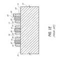
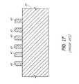
- Such a methodis illustrated in FIGS. 1A-1F and described in U.S. Pat. No. 5,328,810, issued to Lowrey et al., the entire disclosure of which is incorporated herein by reference and made part of this specification. For convenience, the method will also be briefly outlined here.
- photolithographyis first used to form a pattern of lines 10 in a photoresist layer overlying a layer 20 of an expendable material and a substrate 30 .
- the layers shown in FIG. 1are all shown schematically in cross-section.
- the patternis then transferred by an etch step (preferably anisotropic) to the layer 20 , forming placeholders, or mandrels, 40 . If the etch is anisotropic, the mandrels have approximately vertical sides, as shown.
- the photoresist lines 10can be stripped and the mandrels 40 can be isotropically etched to increase the distance between neighboring mandrels 40 , as shown in FIG. 1C .
- pitch multiplicationincreases the density of features by reducing pitch. Pitch thus has at least two meanings: the linear spacing between identical features in a repeating pattern; and the density or number of features per linear distance. The conventional terminology is retained herein.
- the critical dimension (CD) of a mask scheme or circuit designis the scheme's minimum feature dimension, or the measurement of the smallest width of the smallest feature that exists in that design or scheme. Due to factors such as geometric complexity and different requirements for critical dimensions in different parts of an integrated circuit, typically not all features of the integrated circuit will be pitch multiplied. Furthermore, pitch multiplication entails many additional steps relative to conventional lithography; the additional steps can involve considerable additional expense. Pitch multiplication often provides less control over the resulting features than that provided by direct patterning without pitch multiplication, because the spacer pattern merely follows the outlines of the directly patterned features. Thus, pitch multiplication is typically thought useful only for regularly spaced lines, such as conductive lines for a memory array.
- the inventioncomprises a method of forming isolated features in an integrated circuit.
- the methodcan comprise providing a substrate overlaid by multiple layers of masking material and creating a first series of selectively definable lines in a first layer of masking material.
- the methodcan further comprise reducing the pitch of the first series of selectively definable lines using a spacer material to create a first arrangement of masking features having a smaller pitch than the first series of selectively definable lines.
- the first arrangement of masking featurescan comprise pitch-reduced masking lines separated by pitch-reduced spaces and can correspond to a first pattern.
- the inventioncomprises a method for forming features in an array.
- the methodcan comprise reducing the pitch of a column of first photodefinable lines to form a column pattern.
- the methodcan also comprise reducing the pitch of a row of second photodefinable lines to form a row pattern that crosses the column pattern.
- the row patterncan have row lines and row spaces.
- the row linescan mask off unexposed portions of the underlying column pattern, and the row spaces can leave exposed portions of the underlying column pattern.
- the methodcan further comprise removing at least some of the exposed portions of the column pattern to define a combined mask layer.
- the inventioncomprises a mask pattern for an integrated circuit.
- the mask patterncan comprise a first series of elongate masking lines and a second series of elongate masking lines that intersects the first series of elongate masking lines.
- each series of linescan have a pitch that is smaller than the pitch achievable through photolithography.
- the inventioncomprises an arrangement of isolated features formed as part of an integrated circuit manufacturing process.
- the arrangementcan have a first row of elongate features formed from spacer material and a second row of elongate features formed from spacer material.
- the elongate features in the second rowcan cross the elongate features in the first row such that each elongate feature in one row crosses multiple elongate features in the other row.
- the inventioncomprises a method of forming a feature array for an integrated circuit.
- the methodcan include forming a first, pitch-multiplied feature array in a first mask layer, the features being elongate with an axis of elongation.
- the first feature arraycan have a first pattern.
- the methodcan further include forming a second, pitch-multiplied feature array in a second mask layer, the second pitch-multiplied feature array having elongate features with an axis of elongation that is not parallel to the axis of the elongate features of the first feature array.
- the second feature arraycan have a second pattern.
- the methodcan further include consolidating the first and second patterns into a combined third pattern, the third pattern corresponding to an arrangement of features in a single vertical level of the integrated circuit.
- the inventioncomprises a system for processing information in electrical format.
- the systemcan include at least one electrical circuit.
- the systemcan further include densely-spaced features in a repeating pattern, formed in a layer of material in the electrical circuit.
- Each featurecan have a first width of less than 60 nanometers and a first length of less than 10 times the first width.
- each featurecan be spaced apart from adjacent features by less than 120 nanometers.
- FIGS. 1A-1Fare schematic, cross-sectional side views of mask lines, formed in accordance with a prior art pitch-multiplication method as described above.
- FIG. 2is a schematic, cross-sectional side view of masking and substrate layers used to form an integrated circuit.
- FIG. 3shows the structure of FIG. 2 after photolithographic patterning of a first resist layer.
- FIG. 4shows the structure of FIG. 3 after an etch has reduced the size of the features in the pattern of FIG. 3 .
- FIG. 5shows a schematic, cross-sectional side view of masking and substrate layers used to form an integrated circuit after the pattern of FIG. 4 has been extended into underlying layers.
- FIG. 6shows the structure of FIG. 5 after overlying layers have been stripped.
- FIG. 8shows the structure of FIG. 7 after a spacer etch and subsequent etch, leaving a pattern of free-standing spacers that has been extended into an underlying layer.
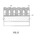
- FIG. 9shows the structure of FIG. 8 after blanket deposition of a filler material.
- FIGS. 10A-10Dshow the structure of FIG. 9 after a CMP process or dry etch has removed the spacers and excess filler material.
- FIG. 10Ashows a schematic plan view of the surface.
- FIG. 10Bshows a schematic cross-sectional side view taken along lines 10 B- 10 B of FIG. 10A .
- FIG. 10Cshows a schematic, cross-sectional side view taken along lines 10 C- 10 C of FIG. 10B .
- FIG. 10Dshows a schematic, cross-sectional side view taken along lines 10 D- 10 D of FIG. 10B .
- FIGS. 11A-11Dshow the structure of FIG. 10 after deposition of multiple new layers.
- FIG. 11Ashows a schematic plan view of the surface.
- FIG. 11Bshows a schematic cross-sectional side view taken along lines 11 B- 11 B of FIG. 11A .
- FIG. 11Cshows a schematic, cross-sectional side view taken along lines 11 C- 11 C of FIG. 11B .
- FIG. 11Dshows a schematic, cross-sectional side view taken along lines 11 D- 11 D of FIG. 11B .
- FIGS. 12A-12Dshow the structure of FIG. 11 after photolithographic patterning of a second resist layer.
- FIG. 12Ashows a schematic plan view of the surface.
- FIG. 12Bshows a schematic cross-sectional side view taken along lines 12 B- 12 B of FIG. 12A .
- FIG. 12Cshows a schematic, cross-sectional side view taken along lines 12 C- 12 C of FIG. 12B .
- FIG. 12Dshows a schematic, cross-sectional side view taken along lines 12 D- 12 D of FIG. 12B .
- FIGS. 13A-13Dshow the structure of FIG. 12 after an etch has reduced the size of the features in the pattern of FIG. 12 .
- FIG. 13Ashows a schematic plan view of the surface.
- FIG. 13Bshows a schematic cross-sectional side view taken along lines 13 B- 13 B of FIG. 13A .
- FIG. 13Cshows a schematic, cross-sectional side view taken along lines 13 C- 13 C of FIG. 13B .
- FIG. 13Dshows a schematic, cross-sectional side view taken along lines 13 D- 13 D of FIG. 13B .
- FIGS. 14A-14Dshow the structure of FIG. 13 after the pattern of the features of FIGS. 13A-13D has been extended into underlying layers to partially expose the crossing underlying pattern.
- FIG. 14Ashows a schematic plan view of the surface.
- FIG. 14Bshows a schematic cross-sectional side view taken along lines 14 B- 14 B of FIG. 14A .
- FIG. 14Cshows a schematic, cross-sectional side view taken along lines 14 C- 14 C of FIG. 14B .
- FIG. 14Dshows a schematic, cross-sectional side view taken along lines 14 D- 14 D of FIG. 14B .
- FIGS. 15A-15Dshow the structure of FIG. 14 after overlying layers have been stripped.
- FIG. 15Ashows a schematic plan view of the surface.
- FIG. 15Bshows a schematic cross-sectional side view taken along lines 15 B- 15 B of FIG. 15A .
- FIG. 15Cshows a schematic, cross-sectional side view taken along lines 15 C- 15 C of FIG. 15B .
- FIG. 15Dshows a schematic, cross-sectional side view taken along lines 15 D- 15 D of FIG. 15B .
- FIGS. 16A-16Dshow the structure of FIG. 15 after blanket deposition of a spacer material.
- FIG. 16Ashows a schematic plan view of the surface.
- FIG. 16Bshows a schematic cross-sectional side view taken along lines 16 B- 16 B of FIG. 16A .
- FIG. 16Cshows a schematic, cross-sectional side view taken along lines 16 C- 16 C of FIG. 16B .
- FIG. 16Dshows a schematic, cross-sectional side view taken along lines 16 D- 16 D of FIG. 16B .
- FIGS. 17A-17Dshow the structure of FIG. 16 after a spacer etch and subsequent etch (that has removed the mandrels), leaving a pattern of free-standing spacers that are orthogonal to the underlying pattern.
- FIG. 17Ashows a schematic plan view of the surface.
- FIG. 17Bshows a schematic cross-sectional side view taken along lines 17 B- 17 B of FIG. 17A .
- FIG. 17Cshows a schematic, cross-sectional side view taken along lines 17 C- 17 C of FIG. 17B .
- FIG. 17Dshows a schematic, cross-sectional side view taken along lines 17 D- 17 D of FIG. 17B .
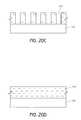
- FIGS. 18-20illustrate a process flow that can be used in conjunction with the structure of FIG. 17 to create a mask grid with small holes that are densely spaced in an advantageous manner.
- FIGS. 18A-18Eshow the structure of FIG. 17 after an etch (e.g., a silicon dioxide etch) has removed portions of several exposed layers, while leaving intact one of the stripe materials of exposed portions of the underlying pattern.
- FIG. 18Ashows a schematic plan view of the surface.
- FIG. 18Bshows a schematic cross-sectional side view taken along lines 18 B- 18 B of FIG. 18A .
- FIG. 18Cshows a schematic, cross-sectional side view taken along lines 18 C- 18 C of FIGS. 18A and 18B .
- FIG. 18Dshows a schematic, cross-sectional side view taken along lines 18 D- 18 D of FIGS. 18A and 18B .
- FIG. 18Eshows a schematic, cross-sectional side view taken along line 18 E- 18 E of FIG. 18A .
- FIGS. 19A-19Dshow the structure of FIG. 18 after extending the pattern of two overlying layers into an underlying mask or temporary layer, forming holes in the underlying layer.
- the underlying temporary layeris amorphous carbon.
- FIG. 19Ashows a schematic plan view of the surface.
- FIG. 19Bshows a schematic cross-sectional side view taken along lines 19 B- 19 B of FIG. 19A .
- FIG. 20Cshows a schematic, cross-sectional side view taken along lines 19 C- 19 C of FIG. 19B .
- FIG. 19Dshows a schematic, cross-sectional side view taken along lines 19 D- 19 D of FIG. 19B .
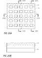
- FIGS. 20A-20Dshow the structure of FIG. 19 after overlying layers have been stripped to leave a pattern of holes in the lower temporary or mask (e.g., amorphous carbon) layer.
- FIG. 20Ashows a schematic plan view of the surface.
- FIG. 20Bshows a schematic cross-sectional side view taken along lines 20 B- 20 B of FIG. 20A .
- FIG. 20Cshows a schematic, cross-sectional side view taken along lines 20 C- 20 C of FIG. 20A .
- FIG. 20Dshows a schematic, cross-sectional side view taken along lines 20 D- 20 D of FIG. 20A .
- FIG. 21Ashows the structure of FIG. 20C after the pattern of holes in the third temporary layer has been extended into the substrate, the third temporary layer has been removed, and the holes have been filled with conductive material.
- FIG. 21Bshows the structure of FIG. 21A after the overflow conductive material has been etched away.
- FIGS. 22-25illustrate a process flow that can be used in conjunction with the structure of FIG. 17 to create small mask pillars that are densely packed in an advantageous manner.
- FIGS. 22A-22Eshow the structure of FIG. 17 after an etch (e.g., an amorphous silicon etch) to remove one of the stripe materials of exposed portions of the underlying pattern.
- FIG. 22Ashows a schematic plan view of the surface.
- FIG. 22Bshows a schematic cross-sectional side view taken along lines 22 B- 22 B of FIG. 22A .
- FIG. 22Cshows a schematic, cross-sectional side view taken along lines 22 C- 22 C of FIGS. 22A and 22B .
- FIG. 22Dshows a schematic, cross-sectional side view taken along lines 22 D- 22 D of FIGS. 22A and 22B .
- FIG. 22Eshows a schematic, cross-sectional side view taken along line 22 E- 22 E of FIG. 22A .
- FIGS. 23A-23Dshow the structure of FIG. 22 after a selective etch, (e.g., a silicon dioxide etch) has etched down portions of exposed materials in FIG. 22 to expose portions of an underlying mask or temporary layer.
- a selective etche.g., a silicon dioxide etch
- the underlying temporary layeris amorphous carbon.
- the selective etchhas not removed islands of one of the stripe materials (e.g., silicon) that remain in place over the temporary layer.
- FIG. 23Ashows a schematic plan view of the surface.
- FIG. 23Bshows a schematic cross-sectional side view taken along lines 23 B- 23 B of FIG. 23A .
- FIGS. 24A-24Bshow the structure of FIG. 23 after etching the exposed portions of the underlying temporary layer.
- the island patternhas thus been extended into the underlying material, leaving standing pillars or posts protected by silicon caps.
- FIGS. 25A-25Bshow the structure of FIG. 24 after a silicon etch has removed the silicon caps from the pillars or posts.
- the pillarscan be used as a mask for an underlying material.
- FIGS. 26-27illustrate an alternative process flow that can be used in conjunction with the structure of FIG. 17 to create small mask pillars, posts or islands that are densely and/or evenly spaced in an advantageous manner.
- FIGS. 26A-26Dshow the structure of FIG. 17 after a nonselective etch (for example a sputter etch or reactive ion etch) that etches exposed portions of both striped materials, exposing crossing lines of an underlying mask or temporary layer.
- the underlying temporary layeris amorphous carbon.
- FIG. 26Ashows a schematic plan view of the surface.
- FIG. 26Bshows a schematic cross-sectional side view taken along lines 26 B- 26 B of FIG. 26A .
- FIG. 26Cshows a schematic, cross-sectional side view taken along lines 26 C- 26 C of FIG. 26B .
- FIG. 26Dshows a schematic, cross-sectional side view taken along lines 26 D- 26 D of FIG. 26B .
- FIGS. 27A-27Dshow the structure of FIG. 26 after the spacer pattern has been extended into an underlying layer (i.e., an amorphous carbon layer).
- FIG. 27Ashows a schematic plan view of the surface.
- FIG. 27Bshows a schematic cross-sectional side view taken along lines 27 B- 27 B of FIG. 27A .
- FIG. 27Cshows a schematic, cross-sectional side view taken along lines 27 C- 27 C of FIG. 27B .
- FIG. 27Dshows a schematic, cross-sectional side view taken along lines 27 D- 27 D of FIG. 27B .
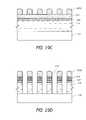
- FIGS. 28A-28Bshow the structure of FIG. 27 after removal of the spacers, one of the stripe materials, and extension of the island pattern into the remaining portions of an underlying layer to leave standing pillars or posts, protected by amorphous silicon caps.
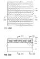
- FIGS. 29 a - 29 bare scanning electron micrographs (SEMs) illustrating a cross-sectional view of a dense array of small holes formed according to the described embodiments.
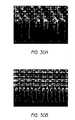
- FIGS. 30 a - 30 bare scanning electron micrographs (SEMs) illustrating a perspective views of a dense array of small holes formed according to the described embodiments.
- FIGS. 31 a - 31 care SEMs illustrating a dense array of small holes formed according to the described embodiments.
- FIG. 30 billustrates a cross section of FIG. 30 a in one dimension
- FIG. 30 cillustrates a cross section of FIG. 30 a in an approximately perpendicular dimension.
- FIGS. 32 a - 32 bare SEMs of an array of small, dense pillars or posts in accordance with the disclosed embodiments.
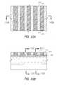
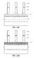
- a partially formed integrated circuit 100is provided.
- a substrate 110is provided below various masking layers 120 - 170 .
- the layers 120 - 170can be etched to form masks for patterning underlying layers or substrate 110 .
- These maskscan be used to form various features, as discussed below.
- the featurescan comprise portions of any of the following: one or multiple transistors, diodes, capacitors, conductive lines, gates, sources, drains, or contacts to any of the above. These components can comprise portions of DRAM or flash memory arrays, NOR logic arrays, NAND logic arrays, etc.
- the featuresare formed from a substrate material that comprises a semi-conducting material.
- the semi-conducting materialcan be silicon, silicon-germanium compounds, or III-V materials.
- the term “substrate”can refer not only to the substrate layer 110 , but also to any layer that underlies another layer.
- the term “substrate”can also describe a layer or layers that have features or structures formed within them as a result of a semiconductor process (e.g., etching, doping, depositing, etc.) controlled by overlying masking layers.
- the term “pattern”can refer to an array or series of shapes that would be visible on a surface if viewed from above.
- a patterncan refer to the ensemble of shapes that correspond to a cross-section or shadow of features formed in one or multiple layers. The pattern is generally not the features themselves, but rather the design corresponding to the sizes and arrangement of the features.
- a patterncan be defined by a combination of patterns derived from multiple overlying or side by side layers.
- a patterncan originate in one layer, such as a photodefinable layer, and then be transferred to another layer, such as a temporary layer or a hard mask layer. The pattern is said to be transferred to lower layers even if feature sizes and spacings are altered (e.g., by the feature shrink step noted above).
- a new patterncan be defined by pitch multiplication, whereby two or more features in the second pattern replace one feature of the first pattern.
- a pattern in one layercan be derived from one or more patterns in another previous or overlying layer.
- a patterncan be said to be derived from another pattern even if the features in the resulting layer do not exactly resemble those features which gave rise to the original pattern, but rather the underlying pattern generally follows the outline of the overlying pattern with minor deviations in dimensions.
- the term “to pattern”can also be used as a verb and means to create or form a pattern.
- An arrangement of features formed in a particular layercan give rise to a pattern.
- An arraycan also give rise to a pattern.
- An arrayis a collection of electrical components or features, formed in a repeating configuration, that can span multiple layers of an integrated circuit. As described above, multiple cells can form a memory array for a DRAM or NAND flash memory circuit, for example, or a logic array.
- the materials for the layers 120 - 170 overlying the substrate 110are preferably chosen based upon consideration of the chemistry and process conditions for the various pattern forming and pattern transferring steps discussed herein. Because the layers between a topmost selectively definable layer 120 —which preferably is definable by a lithographic process—and the substrate 110 will preferably function to transfer a pattern derived from the selectively definable layer 120 to the substrate 110 , the layers between the selectively definable layer 120 and the substrate 110 are preferably chosen so that they can be selectively etched relative to other exposed materials. A material is considered selectively, or preferentially, etched when the etch rate for that material is at least about two times greater, preferably about ten times greater and, most preferably, at least about forty times greater than that for surrounding materials.
- the selectively definable layer 120overlies a first hard mask, or etch stop, layer 130 , which overlies a first temporary layer 140 , which overlies a second temporary layer 150 , which overlies a second hard mask, or etch stop, layer 160 , which overlies a third temporary layer 170 to be processed (e.g., etched) through a mask, which overlies the substrate layer 110 .
- the third temporary layer 170will serve as the ultimate mask through which etching (or other processing) will be performed.
- amorphous carbonis a preferred material for the third temporary layer because so many other materials-silicon, silicon oxide, silicon nitride, etc.—can be selectively etched without significantly harming the carbon layer.
- the substrate 110may comprise an interlevel dielectric (ILD) layer through which contacts are to be formed.
- ILDinterlevel dielectric
- both the mask and the underlying substrateare exposed to an etchant, which preferentially etches away the substrate material.
- the etchantscan also wear away the mask materials, albeit at a slower rate.
- the maskcan be worn away by the etchant before the pattern transfer is complete.
- hard mask layers 130 and 160advantageously play a protective role, protecting underlying layers from unwanted degradation during etching of overlying layers.
- various other layerssuch as the second hard mask layer 160 itself, may be omitted and overlying mask layers may be sufficient for the desired pattern transfer.
- Higher numbers of mask layersare advantageous for transferring patterns to difficult to etch substrates, such as a substrate comprising multiple materials or multiple layers of materials, or for forming small and high aspect ratio features.
- photoresist materialsinclude argon fluoride (ArF) sensitive photoresist, i.e., photoresist suitable for use with an ArF light source, and krypton fluoride (KrF) sensitive photoresist, i.e., photoresist suitable for use with a KrF light source.
- ArF photoresistsare preferably used with photolithography systems utilizing relatively short wavelength light, e.g., 193 nm.
- KrF photoresistsare preferably used with longer wavelength photolithography systems, such as 248 nm systems.
- the layer 120 and any subsequent resist layerscan be formed of a resist that can be patterned by nano-imprint lithography, e.g., by using a mold or mechanical force to pattern the resist.
- Photoresistis typically patterned by being exposed to radiation through a reticle and then developed.
- radiatione.g., light
- the radiationis focused on parts of the photoresist that are to be retained, e.g., on the areas where the lines—such as lines 124 (see FIG. 3 )—are to be formed.
- the radiationactivates a photosensitive compound, e.g., a photo-induced acid generator (PAG), which decreases the solubility of the photoresist, e.g., by causing it to polymerize.
- Preferred embodimentsmay be applied using any definable material, including positive or negative photoresist.
- a preferred reticle used in testing of some embodimentsis T37Z 46/47reticle.
- the material for the first hard mask layer 130preferably comprises an inorganic material, and exemplary materials include silicon dioxide (SiO 2 ), silicon, or a dielectric anti-reflective coating (DARC), such as a silicon-rich silicon oxynitride.
- the first hard mask layer 130is a dielectric anti-reflective coating (DARC).
- DARCdielectric anti-reflective coating
- hard mask layer 130can serve both as an intermediate hard mask and to reduce reflections during lithography.
- DARC material for the first hard mask layer 130can be particularly advantageous for forming patterns having pitches near the resolution limits of a photolithographic technique.
- the DARCcan enhance resolution by minimizing light reflections, thus increasing the precision with which photolithography can define the edges of a pattern.
- an organic bottom anti-reflective coating (BARC)(not shown) can similarly be used in addition to or in place of the first hard mask layer 130 to control light reflections.
- the second temporary layer 150is preferably formed of amorphous silicon.
- amorphous siliconcan be selectively etched while other adjacent materials (such as oxide layers) remain intact.
- the second hard mask, or etch stop layer 160preferably comprises silicon dioxide (SiO 2 ), silicon, or a dielectric anti-reflective coating (DARC), such as a silicon-rich silicon oxynitride, or aluminum oxide (Al 2 O 3 ).
- the first hard mask layer 160is a DARC.
- the third temporary layer 170is preferably formed of amorphous carbon, which has excellent etch selectivity relative to many materials. Benefits of amorphous carbon are further discussed above with respect to the first temporary layer 140 .
- the substratecan be a silicon wafer used for formation of integrated circuits.
- Various substrate materialscan be used.
- the thicknesses of the layers 120 - 170are preferably chosen depending upon compatibility with the etch chemistries and process conditions described herein. For example, when transferring a pattern from an overlying layer to an underlying layer by selectively etching the underlying layer, materials from both layers are removed to some degree.
- the upper layeris preferably thick enough so that it is not worn away over the course of the pattern transfer.
- the hard mask layersare advantageously thin so that their transfer or removal can occur quickly, exposing surrounding materials to less wear.
- the selectively definable layer 120is a photodefinable layer preferably between about 100-250 nm thick and, more preferably, between about 130-200 nm thick.
- the first hard mask layer 130e.g., SiO 2 or DARC
- the first temporary layer 140e.g., amorphous carbon
- the second temporary layer 150(e.g., amorphous silicon) is preferably between about 30-50 nm thick and, more preferably, between about 35-45 nm thick.
- the second hard mask layer 160(e.g., SiO 2 or DARC) is preferably between about 10-30 nm thick and, more preferably, about 15 nm thick.
- the third temporary layer 170(e.g., amorphous carbon) is preferably between about 100-300 nm thick and, more preferably, between about 150-250 nm thick.
- various layers discussed hereincan be formed by various methods known to those of skill in the art.
- various vapor deposition processessuch as chemical vapor deposition
- a low temperature chemical vapor deposition processis used to deposit the hard mask layers or any other materials, e.g., spacer material, over carbon.
- Such low temperature deposition processesadvantageously prevent chemical or physical disruption of the underlying amorphous carbon layer.
- Spin-on-coating processescan be used to form photodefinable layers.
- amorphous carbon layerscan be formed by chemical vapor deposition using a hydrocarbon compound, or mixtures of such compounds, as carbon precursors.
- Exemplary precursorsinclude propylene, propyne, propane, butane, butylene, butadiene and acetylene.
- a suitable method for forming amorphous carbon layersis described in U.S. Pat. No. 6,573,030 B1, issued to Fairbairn et al. on Jun. 3, 2003, the entire disclosure of which is incorporated herein by reference and made part of this specification.
- the amorphous carbonmay be doped.
- a suitable method for forming doped amorphous carbonis described in U.S. patent application Ser. No. 10/652,174 to Yin et al., the entire disclosure of which is incorporated herein by reference and made part of this specification.
- a pattern of spacersis formed by pitch multiplication and used to create an underlying striped structure (see FIG. 10 ) for subsequent method steps.
- One example of an etch sequence for this phaseis the following: 1) deposition of multiple layers; 2) photolithographic patterning of a first layer; 3) shrinking of features; 4) extension of pattern into underlying layers; 5) removal of remaining portions of overlying layers; 6) blanket deposition of spacer material; 7) spacer etch; 8) removal of spacer mandrels; 9) extension of spacer pattern into underlying material; 10) blanket deposition of a filler material; 11) removal of spacers; and 12) planarization.
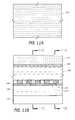
- a pattern comprising gaps or spaces 122 delimited by definable material features 124is formed in the definable layer 120 .
- the spaces 122can be formed by, e.g., photolithography, in which the selectively definable layer 120 is exposed to radiation through a reticle and then developed. After being developed, the remaining definable material, photoresist in the illustrated embodiment, forms mask features such as the illustrated lines 124 (shown in cross-section).
- the pitch of the lines 124is equal to the sum of the width of a line 124 and the width of a neighboring space 122 .
- the pitchis preferably at or near the limits of the photolithographic technique used to pattern the definable layer 120 .
- the pitch of the lines 124can be about 200 nm.
- the pitchmay be at the minimum pitch of the photolithographic technique and the spacer pattern discussed below can advantageously have a pitch below the minimum pitch of the photolithographic technique.
- a preliminary stepcan comprise creating a series of photoresist lines 124 .
- photolithographycan be used to form a plurality of lines in a mask material.
- Conventional photolithographycan form lines having a pitch no smaller than that definable by photons.
- subsequent pitch multiplicationcan form lines having a pitch that is smaller than that definable by conventional photolithography.
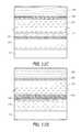
- FIG. 4shows the structure of FIG. 3 after the lines 124 have been shrunk by an isotropic etch to create modified lines 124 a.
- the spaces 122can optionally be widened or narrowed to a desired dimension. For example, as illustrated in FIG. 6 , the spaces 122 have been widened by etching the photoresist lines 124 , to form modified spaces 122 a and modified lines 124 a.
- the photoresist lines 124are preferably reduced in size using an isotropic etch, such as a sulfur oxide plasma, e.g., a plasma comprising SO 2 , O 2 , N 2 and Ar, or any other suitable plasma.
- Two other plasmas that can be usedare an HBr/O 2 plasma or a Cl 2 /O 2 plasma.
- the isotropic etchdegrades the exposed surfaces from all directions.
- the corners of lines 124 ahave been depicted as slightly rounded in FIG. 4 .
- the extent of the etchis preferably selected so that the widths of the lines 124 a are substantially equal to the desired spacing between the later-formed spacers 182 , as will be appreciated from the discussion of FIGS. 7-8 .
- this etchallows the lines 124 a to be narrower than would otherwise be possible using the photolithographic technique used to pattern the photodefinable layer 120 .
- this etchcan reduce their size even further, taking them below that resolution limit.
- the etchcan smooth the edges of the lines 124 a, thus improving the uniformity of those lines.
- the spaces 122 a between the lines 124 acan be narrowed by expanding the lines 124 to a desired size.
- additional material(not shown) can be deposited over the lines 124 , or the lines 124 can be chemically reacted to form a material (not shown) having a larger volume to increase their size.
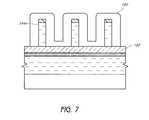
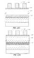
- the modified lines 124 adefine the dimensions of placeholders or mandrels along which a pattern of spacers 182 ( FIG. 8 ) will be formed after transfer of the pattern to an underlying layer ( FIGS. 5 and 6 ) and blanket deposition of a spacer material 180 ( FIG. 7 ).
- the temporary layer 140can be omitted and the spacer material can be deposited directly on the photo-defined lines 124 or the thinner lines 124 a.
- the pattern of the lines 124can be transferred to underlying layers without first being trimmed or having their width's reduced as described above.
- a pattern corresponding to that of lines 124can be formed in the temporary layer 140 and the features of that pattern can be reduced in width with a shrink step.
- the pattern in the photodefinable layer 120is preferably transferred to the first temporary layer 140 to allow for later deposition of a layer 180 of spacer material ( FIG. 7 ).
- the temporary layer 140is preferably formed of a material that can withstand the process conditions for spacer material deposition and etch, discussed below.
- the material forming the temporary layer 140preferably has a higher heat resistance than photoresist and is preferably selected such that it can be selectively removed relative to the material for the spacers 182 ( FIG. 8 ) and the underlying layer 150 .
- the layer 140is preferably formed of amorphous carbon.
- the pattern of lines 124 a and spaces 122 a in FIG. 4can be extended into, or transferred to underlying layers. This pattern extension can be accomplished by selectively etching the materials that form layers 130 and 140 , while lines 124 a form a protective mask that prevents the etchant from removing the material located underneath lines 124 a.
- an anisotropic etchcan be used, such as an etch using a fluorocarbon plasma.
- a wet (isotropic) etchmay also be suitable if the hard mask layer 130 is thin.
- Preferred fluorocarbon plasma etch chemistriesinclude CF 4 , CFH 3 , CF 2 H 2 and CF 3 H for etching the preferred DARC material.
- an SO 2 -containing plasmae.g., a plasma containing SO 2 , O 2 and Ar
- the SO 2 -containing plasmacan etch carbon of the preferred temporary layer 140 at a rate greater than 20 times and, more preferably, greater than 40 times the rate that the hard mask layer 130 is etched.
- a suitable SO 2 -containing plasmais described in U.S. patent application Ser. No. 10/931,772 to Abatchev et al., filed Aug. 31, 2004, entitled Critical Dimension Control, (Atty. docket No. MICRON.286A; Micron Ref. No. 2003-1348), the entire disclosure of which is incorporated herein by reference and made part of this specification.
- FIG. 5shows lines 124 a intact after the pattern has been extended into the first temporary layer 140
- the SO 2 -containing plasmacan simultaneously etch the temporary layer 140 and also remove the remaining portion of definable layer 120 .
- the remaining portions of the layer 120can be stripped away using a selective etch.
- the remaining portions of 120can be etched away during an amorphous carbon etch step such as the step that extends the pattern down into the layer 140 .
- the line pattern originally formed in the definable layer 120has been transferred to the hard mask and temporary layers 130 and 140 .
- the transferred patternis approximately the same as the line pattern originally formed in layer 120 ; the transferred pattern has lines 144 a and spaces 142 a that generally correspond to lines 124 a and spaces 122 a, respectively.
- portions of the hard mask layer 130remain in place as protective caps on the lines 144 a. These portions of the layer 130 can act as etch stops in subsequent steps.
- a patternis formed in an overlying layer and later transferred to an underlying layer.
- the illustrated walls of the features formed in layers 130 and 140are vertical, where these layers have been etched.
- directional or anisotropic etchescan be used.
- etching processescan alter the precision with which a pattern in an overlying layer corresponds to a pattern created in an underlying layer.
- pattern transfer from layer to layeris generally illustrated schematically to be a precise process, with vertical walls, such precision may be difficult to achieve in practice.
- pattern transferis intended to encompass general correspondence between underlying and overlying patterns.
- pattern transferis meant to encompass modification of the features originally defining the pattern—for example by enlarging or shrinking those features—where such modification does not change the pitch.
- a layer 180 of spacer materialis preferably blanket deposited so that it conforms to the exposed surfaces, including the second temporary layer 150 and the lines 144 a.
- portions of the hard mask layer 130can be left in place—to subsequently act as CMP etch stops—on top of lines 144 a when the layer 180 of spacer material is deposited.
- the hard mask portionscan be removed with a selective etch before spacer deposition.
- the spacer materialcan be any material that can act as a mask for transferring a pattern to underlying layers, or that otherwise can allow processing of underlying structures through the mask being formed.
- the spacer materialpreferably: 1) can be deposited with good step coverage; 2) can be deposited at a temperature compatible with the temporary layer 140 and underlying layers; and 3) can be selectively etched relative to the temporary layer 140 and any layer directly underlying the temporary layer 140 .
- Preferred materialsinclude silicon oxides and nitrides.
- the spacer materialis preferably deposited by chemical vapor deposition or atomic layer deposition.
- the layer 180is preferably deposited to a thickness of between about 20-60 nm and, more preferably, about 20-50 nm.
- the step coverageis about 80% or greater and, more preferably, about 90% or greater.
- FIG. 8shows the structure of FIG. 7 after a spacer etch and subsequent etch, leaving a pattern of free-standing spacers that has been extended into an underlying layer.
- the spacer etchcan comprise an anisotropic etch to remove spacer material from horizontal surfaces.
- the spacer etchcan be performed using a fluorocarbon plasma.
- the spacer etchcan also be performed using HBr/Cl plasma for a silicon spacer material. (Note that preferred embodiments use silicon oxide spacers, however). After a spacer etch is performed, it can leave behind a pattern of elongate spacers having effectively reduced pitch relative to the lines.
- the remaining portions of hard mask layer 130 (if still present) and the temporary layer 140are next removed to leave freestanding spacers 182 .
- the remaining portions (in the form of lines 144 a ) of the first temporary layer 140are selectively removed, preferably using a sulfur-containing plasma etch such as an etch using SO 2 . In this way, features of one pattern are removed to leave behind another pattern formed by the spacers.
- pitch-reductionhas been performed using a spacer material to create masking features.
- the masking features formed in this waycan have a smaller pitch than the photoresist lines and can comprise pitch-reduced masking lines separated by pitch-reduced spaces; pitch multiplication has been accomplished.
- the pitch of the pattern formed by spacers 182is roughly half that of the pattern formed by photoresist lines 124 a and spaces 122 a ( FIGS. 3-5 ), where the pitch was originally determined by photolithography.
- a spacer pattern having a pitch of about 100 nmcan be formed.
- the pattern formed by the spacers 182can be extended into the underlying second temporary layer 150 .
- the extensioncan be accomplished with a selective etch chemistry.
- a selective etch chemistryFor example, if the spacers 182 are formed from silicon dioxide and the underlying layer 150 is formed from amorphous silicon, an etch can remove the latter while leaving the former largely intact.
- a preferred etchincludes a physical component and preferably can also include a chemical component and can be, e.g., a reactive ion etch (RIE), such as an HBr/Cl 2 etch.
- RIEreactive ion etch
- Such an etchcan be performed, for example, using a LAM TCP9400 (available commercially from LAM Research Corporation of Fremont, Calif.) flowing about 0-50 sccm Cl 2 and about 0-200 sccm HBr at about 7-60 mTorr pressure with about 300-1000 W top power and about 50-250 W bottom power.
- LAM TCP9400available commercially from LAM Research Corporation of Fremont, Calif.
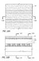
- FIG. 9shows the structure of FIG. 8 after blanket deposition of a filler material 190 .
- the filler material 190is advantageously formed from silicon dioxide (SiO 2 ).
- the spacers 182 and the filler material 190are formed from the same or similar materials, as will be better understood from the discussion of FIGS. 17-20 , 22 - 23 , and 26 - 27 below.
- the spacers 182 and the filler material 190can both be formed from silicon dioxide.
- One preferred process for depositing the filler material 190i.e., silicon dioxide
- Applied Materials' Producer® HARPTM system.(HARP stands for “High Aspect Ratio Process.”)
- the spacers 182can be removed before the filler material 190 is deposited.
- a wet etchcan be used to remove the spacers if the hard mask layer 160 is formed from a DARC material. Removal of the spacers 182 can allow good coverage by the filler material 190 .
- FIGS. 10-20 , 22 - 23 , and 26 - 27each illustrate at least four corresponding views, lettered A-D as follows: 10 A- 10 D, 11 A- 11 D, etc.
- the views designated with an “A”consistently show a top or plan view, where hatching has been included for convenience.
- the views B-Cconsistently show cross sections of the same structure depicted in the corresponding figure A.
- those views designated with a “B”consistently show the structure in the same orientation as other views designated with a “B.”
- the orientationsare also similar for “C” designations, and likewise for “D” designations.
- FIGS. 10A-10Dshow the structure of FIG. 9 after removal of the spacers 182 and a portion of the filler material 190 , through, for example, a chemical mechanical polishing (CMP) process.
- CMPchemical mechanical polishing
- a dry etch or a plasma etchcan also be used for planarization.
- a thin etch stop layeris preferably added between the hard mask layer 160 and the temporary layer 150 .
- the etch stop layercan be formed from Si 3 N 4 , for example.
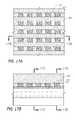
- FIG. 10Ashows a schematic plan view of the surface after the planarization.
- the surfaceexhibits a striped pattern with alternating stripes of the filler material 212 , which is amorphous silicon, for example, and the stripes 214 , which can be silicon dioxide, for example.
- the stripes 212 of amorphous siliconhave been formed in the second temporary layer 150 and the stripes 214 of silicon dioxide are the remaining portions of the filler material 190 that fill the spaces between the stripes 212 .
- the surface in FIG. 10Ais depicted with cross-hatching to show the material that comprises the striped structures.
- the stripes 212preferably have widths 213 in a range of approximately 30-70 nm.
- the stripes 214preferably have widths 215 in a range of approximately 30-70 nm. More preferably, the stripes 212 and 214 each have widths 213 and 215 , respectively, of approximately 50 nm. In the latter case, the pattern formed by the stripes has a pitch of approximately 100 nm.
- FIG. 10Bshows a schematic cross-sectional side view taken along lines 10 B- 10 B of FIG. 10A .
- This viewreveals that the two sets of stripes are formed on the same “level.”
- levelis used to designate a portion of the integrated circuit that is generally located in a thick plane that is parallel to and equidistant from the plane of the surface of the substrate 110 .
- the layer 160is located at a different level from that of layer 170 , but the stripes 212 and the stripes 214 are located at the same level.
- the term “layer”is generally used to refer to a portion of the integrated circuit formed from the same material and deposited together.
- FIG. 10Cshows a schematic, cross-sectional side view taken along lines 10 C- 10 C of FIG. 10B .
- FIG. 10Dshows a schematic, cross-sectional side view taken along lines 10 D- 10 D of FIG. 10B .
- a pattern of spacershas been formed by pitch multiplication and used to create an underlying striped structure or “first pattern” derived from and pitch multiplied relative to the pattern of the first resist mask.
- a second pattern of spacersis formed by pitch multiplication and used to create an overlying striped structure (see FIG. 17 ) that crosses the underlying striped structure of FIG. 10 .
- One example of an etch sequence for this phaseis the following: 1) deposition of multiple layers; 2) photolithographic patterning of an overlying layer; 3) shrinking of features; 4) extension of pattern into underlying layers; 5) removal of remaining portions of overlying layers; 6) blanket deposition of spacer material; 7) spacer etch; 8) removal of spacer mandrels.
- FIGS. 11A-11Dshow the structure of FIG. 10 after deposition of multiple new masking layers, 320 - 340 .
- the pattern having the stripes 212 and the stripes 214now underlies multiple new layers of material.
- layers 320 - 340can also be etched to form masks for patterning underlying layer(s) of substrate 110 .
- These maskscan be used to form various features, as discussed below.
- the featurescan comprise portions of one or multiple integrated circuit components.
- FIG. 11Ashows a schematic plan view of the surface.
- FIG. 11Bshows a schematic cross-sectional side view taken along lines 11 B- 11 B of FIG. 11A .
- FIG. 11Cshows a schematic, cross-sectional side view taken along lines 11 C- 11 C of FIG. 11B .
- FIG. 11Dshows a schematic, cross-sectional side view taken along lines 11 D- 11 D of FIG. 11B .
- masking layer 320preferably has similar properties to those described above with respect to layer 120 .
- layer 330preferably has similar properties to those described above with respect to layer 130 .
- the fourth temporary layer 340preferably has similar properties to those described above with respect to the layer 140 .
- the materials for layers 320 - 340 overlying the substrate 110are preferably chosen based upon consideration of the chemistry and process conditions for the various pattern forming and pattern transferring steps discussed herein. Such layers are also preferably chosen so that they can be selectively etched relative to other exposed materials.
- the second selectively definable layer 320overlies a third hard mask, or etch stop, layer 330 , which overlies a fourth temporary layer 340 , which overlies the level having the stripes 212 and 214 .
- a third hard mask, or etch stop, layer 330which overlies a fourth temporary layer 340 , which overlies the level having the stripes 212 and 214 .
- Underlying levels 160 and 170 , as well as substrate 110remain intact.
- one or more of the layers 320 - 340can be omitted in some embodiments.
- the second selectively definable layer 320is preferably formed of a photoresist, including any photoresist known in the art. All the preferred properties and alternatives described above with reference to the layer 120 also apply to the layer 320 .
- the third hard mask layer 330preferably comprises an inorganic material, and in the illustrated embodiment, the layer 330 is a DARC. All the preferred properties and alternatives described above with reference to the layer 130 also apply to the layer 330 .
- the fourth temporary layer 340is preferably formed of amorphous carbon. All the preferred properties and alternatives described above with reference to the layer 140 also apply to the layer 340 .
- the layer 340is formed from amorphous carbon in some embodiments. Because it is sometime difficult to achieve good step coverage of amorphous carbon deposition, the underlying striped surface has been planarized (see FIG. 10 ).
- the thicknesses of the layers 320 - 340are preferably chosen depending upon compatibility with the etch chemistries and process conditions described herein. Thus, as described above, thicknesses must allow for appropriate pattern transfer, and the hard mask layer 330 is advantageously thin so that its transfer or removal can occur quickly, exposing surrounding materials to less wear.
- the second selectively definable layer 320is a photodefinable layer preferably between about 100-250 nm thick and, more preferably, between about 130-200 nm thick.
- the third hard mask layer 330is preferably between about 10-30 nm thick and, more preferably, between about 15-25 nm thick.
- the fourth temporary layer 340is preferably between about 130-200 nm thick and, more preferably, between about 140-160 nm thick.
- the layers 320 , 330 , and 340can be formed by various methods known to those of skill in the art. For example, the methods described above for forming layers 120 , 130 , and 140 can be used to form layers 320 , 330 , and 340 , respectively.
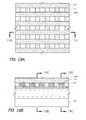
- FIGS. 12A-12Dillustrate a pattern formed in the layer 320 , having lines 324 interspersed with spaces 322 .
- the preferred properties of and methods for forming the lines 124 described above in FIG. 3 et seq.also apply to lines 324 , however, the lines 324 are not parallel to the lines 124 . This can be seen—even though the lines 124 have been removed—by observing that the stripes 212 and the stripes 214 are not parallel to the lines 324 . Thus, because the stripes 212 and 214 are elongate in the same elongate dimension of the lines 124 , the lines 124 and the lines 324 are not parallel.
- the illustrated methodcan be said to call for applying a crossing pattern of photoresist over an underlying pattern.
- one pattern“crosses” a second pattern when an elongate dimension of the first pattern is not aligned with or parallel to an elongate dimension of the second pattern.
- the elongate dimension of the lines 124is aligned with the elongate dimension of the stripes 212 and 214 , but the elongate dimension of the stripes 212 and 214 crosses the elongate dimension of the lines 324 .
- the lines 124can be described as aligned with the stripes 212 and 214
- the stripes 212 and 214can be described as crossing the lines 324 .
- the lines 324not only cross, they cross perpendicularly the stripes 212 and 214 .
- the term “cross”is intended to include all non-parallel angles, not just a 90 degree angle.
- the exemplary features and/or holes formed by the illustrated methodshave a generally rectangular footprint (see, e.g., FIGS. 21A, 25A , and 27 A), other footprints such as skewed quadrangle or diamond-shaped footprints are also contemplated.
- FIGS. 12A-12Dshow the structure of FIG. 11 after photolithographic patterning of an overlying resist layer.
- FIG. 12Ashows a schematic plan view of the surface.
- FIG. 12Bshows a schematic cross-sectional side view taken along lines 12 B- 12 B of FIG. 12A .
- FIG. 12Cshows a schematic, cross-sectional side view taken along lines 12 C- 12 C of FIG. 12B .
- FIG. 12Dshows a schematic, cross-sectional side view taken along the lines 12 D- 12 D of FIG. 12B .
- the pattern created by the series of photoresist lines 324has been formed through conventional photolithography.
- the shrink stepcan be accomplished to make the lines 324 thinner and spacer formation can be accomplished using the modified lines 324 a as mandrels, or the pattern can be transferred to an underlying layer before the shrink step is accomplished.
- the shrink stepis performed on photoresist lines 324 , the pattern is then transferred to an underlying layer, and portions of the underlying layer form spacer mandrels.
- FIGS. 13A-13Dshow the structure of FIG. 12 after the lines 324 have been shrunk, by an isotropic etch, for example, to create modified lines 324 a.
- the shrink stepalso widens the spaces 322 to form modified spaces 322 a.
- FIG. 13Ashows a schematic plan view of the surface.
- FIG. 13Bshows a schematic cross-sectional side view taken along lines 13 B- 13 B of FIG. 13A .
- FIG. 13Cshows a schematic, cross-sectional side view taken along lines 13 C- 13 C of FIG. 13B .
- FIG. 13Dshows a schematic, cross-sectional side view taken along lines 13 D- 13 D of FIG. 13B .
- FIGS. 13A-13Dpreferably shares many characteristics of the features described in conjunction with FIG. 4 . Similar methods to achieve that structure can also be used; preferred etch materials and methods, and desirable configurations are described above.
- the photoresist lines 324are preferably reduced in size using an isotropic etch, such as a sulfur oxide plasma, e.g., a plasma comprising SO 2 , O 2 , N 2 and Ar, or any other suitable plasma.
- a sulfur oxide plasmae.g., a plasma comprising SO 2 , O 2 , N 2 and Ar
- Two other plasmas that can be used, for example,are an HBr/O 2 plasma or a Cl 2 /O 2 plasma.
- the modified lines 324 adefine the dimensions of the placeholders or mandrels along which a pattern of spacers will be formed.
- the pattern of the lines 324can be transferred to underlying layers without first being trimmed or having their width's reduced as described above.
- a pattern corresponding to that of lines 324can be formed in the temporary layer 340 and the features of that pattern can be reduced in width with a shrink step.
- the temporary layer 340can be omitted and the spacer material can be deposited directly on the photo-defined lines 324 or the thinner lines 324 a.
- lines 324 acreate a mask for placeholders or mandrels that will later be formed in the underlying layer 340 , along which a pattern of spacers 382 ( FIG. 17 ) will be formed after blanket deposition of a spacer material 380 ( FIG. 16 ).
- FIGS. 14A-14Dillustrate how the pattern in the photodefinable layer 320 can be extended into the fourth temporary layer 340 .
- FIG. 14Ashows a schematic plan view of the surface.
- FIG. 14Bshows a schematic cross-sectional side view taken along lines 14 B- 14 B of FIG. 14A .
- FIG. 14Cshows a schematic, cross-sectional side view taken along lines 14 C- 14 C of FIG. 14B .
- FIG. 14Dshows a schematic, cross-sectional side view taken along lines 14 - 14 D of FIG. 14B .
- the fourth temporary layer 340preferably has the advantageous properties described above for the second temporary layer 140 such as high heat resistance.
- the pattern of lines 324 a and spaces 322 a in FIGS. 13A-13Dcan be extended into or transferred to underlying layers in a similar way to the way the pattern of lines 124 a and spaces 122 a was transferred to underlying layers, using, for example, a selective etch to transfer the pattern into the hard mask layer 330 and an SO 2 -containing anisotropic plasma etch to transfer the pattern into the fourth temporary layer 340 .
- Preferred and alternative etch chemistriesare described above.
- the described etch stepsremove the portions of the layers 330 and 340 that are not masked by the lines 324 a , thus leaving portions of the stripes 212 and 214 exposed.
- the surfaces visible in FIG. 14Ahave been hatched to reveal the underlying materials of the structure depicted, and to show how the lines 324 a cross the stripes 212 and 214 .
- FIGS. 15A-15Dshow the structure of FIG. 14 after the remaining portions of the overlying layers 320 and 330 have been stripped. Such a process is described above and illustrated in FIGS. 5-6 .
- FIG. 15Ashows a schematic plan view of the surface.
- FIG. 15Bshows a schematic cross-sectional side view taken along lines 15 B- 15 B of FIG. 15A .
- FIG. 15Cshows a schematic, cross-sectional side view taken along lines 15 C- 15 C of FIG. 15B .
- FIG. 15Dshows a schematic, cross-sectional side view taken along lines 15 D- 15 D of FIG. 15B .
- lines 344 and spaces 342exhibit the same crossing pattern previously apparent in overlying layers (see lines 144 a and spaces 142 a, for example).
- the remaining portions of the definable layer 320can be stripped away using a selective etch. Alternatively, the remaining portions of layer 320 can be etched away during the carbon etch step that extends the pattern down into the layer 340 .
- the line pattern originally formed in layer 320has been transferred to the layers 330 and 340 .
- the transferred patternis approximately the same as the line pattern originally formed in layer 320 ; the transferred pattern has lines 344 a and spaces 342 a that generally correspond to lines 324 a and spaces 322 a, respectively.
- portions of the hard mask layer 330remain in place as protective caps on the lines 344 a.
- the lines 344 awill serve as mandrels for the subsequently formed spacers.
- FIGS. 16A-16Dshow the structure of FIG. 15 after blanket deposition of a spacer material 380 over the mandrels 344 a.
- FIG. 16Ashows a schematic plan view of the surface.
- FIG. 16Bshows a schematic cross-sectional side view taken along lines 16 B- 16 B of FIG. 16A .
- FIG. 16Cshows a schematic, cross-sectional side view taken along lines 16 C- 16 C of FIG. 16B .
- FIG. 16Dshows a schematic, cross-sectional side view taken along lines 16 D- 16 D of FIG. 16B .
- the layer 380 of spacer materialpreferably resembles the layer 180 of spacer material described above, in material, in thickness, in coverage, and in mode of deposition.
- portions of the hard mask layer 330have been left in place, although alternative embodiments do not leave such portions in place. If the portions of the hard mask layer 330 are removed before spacer deposition, a selective etch can be used to remove them.
- the material of the layer 380can be different from the materials of the layer 180 , provided that each layer can be selectively etched with respect to other surrounding layers as described herein. Silicon dioxide is a preferred spacer material.
- FIGS. 17A-17Dshow the structure of FIG. 16 after a spacer etch and subsequent etch, leaving a pattern of free-standing spacers.
- FIG. 17Ashows a schematic plan view of the surface.
- FIG. 17Bshows a schematic cross-sectional side view taken along lines 17 B- 17 B of FIG. 17A .
- FIG. 17Cshows a schematic, cross-sectional side view taken along lines 17 C- 17 C of FIG. 17B .
- FIG. 17Dshows a schematic, cross-sectional side view taken along lines 17 D- 17 D of FIG. 17B .
- the spacer etchcan be performed using fluorocarbon plasma.
- the resultis preferably a pattern of elongate spacers having effectively reduced pitch relative to the lines 344 a.
- the remaining portions of hard mask layer 330 (if still present) and the fourth temporary layer 340are next removed to leave freestanding spacers 382 . In this way, features of one pattern are removed to leave behind another pattern formed by the spacers 382 .
- the pitch of the pattern formed by spacers 382is roughly half that of the pattern formed by photoresist lines 344 and spaces 342 .
- the pattern of spacers 382has a pitch of about 140 nm or less.
- the pattern of spacers 382has a pitch of about 100 nm or less.
- a second pattern of spacershas been formed by pitch multiplication and used to create an overlying pattern of lines that crosses the underlying pattern of lines illustrated in FIG. 10 .
- the crossing striped structures depicted in FIG. 17are used to create a grid of material having small holes that can occur at regular intervals in two dimensions (see FIG. 19-20 ).
- etch sequence for this phaseis the following: 1) removal of portions of several exposed layers made from a common material (such as silicon dioxide), while leaving intact one of the materials (such as amorphous silicon) of exposed portions of the underlying stripe materials; 2) extension of two overlying patterns (such as an oxide spacer pattern and a crossing, amorphous silicon strip pattern) into an underlying mask or temporary layer (such as amorphous carbon); and 3) removal of overlying layers to leave a single underlying layer having holes.
- a common materialsuch as silicon dioxide
- overlying patternssuch as an oxide spacer pattern and a crossing, amorphous silicon strip pattern
- temporary layersuch as amorphous carbon
- FIGS. 18A-18Eshow the structure of FIG. 17 after exposed portions of several layers, including the spacers 382 and the stripe 214 , have been selectively etched while the stripe 212 has been left largely intact.
- the stripe 212is formed from amorphous silicon and the spacers and the stripe 214 are formed from silicon dioxide, so the etch is a silicon dioxide etch—that is, it etches silicon dioxide selectively with respect to the amorphous silicon that is also exposed.
- One etch that can be usedis a fluorocarbon etch.
- FIG. 18Ashows a schematic plan view of the surface.
- FIG. 18Bshows a schematic cross-sectional side view taken along lines 18 B- 18 B of FIG. 18A .
- FIG. 18Cshows a schematic, cross-sectional side view taken along lines 18 C- 18 C of FIGS. 18A and 18B .
- FIG. 18Dshows a schematic, cross-sectional side view taken along lines 18 D- 18 D of FIGS. 18A and 18B .
- FIG. 18Eshows a schematic, cross-sectional side view taken along line 18 E- 18 E of FIG. 18A .
- the exposed portions of the stripes 214have been left largely intact by the etch step, while exposed portions of the stripes 214 , the spacers 382 , and the layer 160 have all been etched.
- portions of three different silicon oxide layersare etched by the same etch chemistry. This etch of materials from multiple layers occurs in the illustrated embodiment, as the spacers 382 , the stripes 214 and the second hard mask layer 160 each can be formed from silicon dioxide.
- the materials of these three separate layershave been depicted using stipple of varying weights so that the three layers can be distinguished in the drawings. In some embodiments, each of the three layers can be formed from another common material.
- a “common material”can refer to materials that are similar enough in composition to allow each to be etched together, while maintaining selectivity with respect to surrounding materials. Examples of materials that can thus be considered common for this purpose are the various forms of silicon oxide, such as TEOS, BPSG, LSO, SiO 2 , C-doped oxide, F-doped oxide, porous oxide, SOD, etc. Most preferably, each of these layers is formed using the same composition methods and from the same material (for example, each can be formed from LSO). In other embodiments, the second hard mask layer 160 is formed from a DARC material, as noted above.
- the etch stephas removed the exposed portions of the stripes 214 first because the stripes 214 are not as thick as the spacers 382 . Thus, while the etch has partially removed portions of the spacers 382 , creating modified spacers 382 a, it has penetrated completely the exposed portions of the stripes 214 and the layer 160 . Alternatively, if the layer 160 is formed from a different substance than the spacers 382 and the stripes 214 , a separate selective etch can be used to penetrate down through the layer 160 to the third temporary layer 170 .
- the etchremoves the material of the underlying layer 170 only in the unprotected areas to form small, densely and/or evenly-spaced holes 412 in the layer 170 .
- FIG. 20Cshows the holes in cross section, and reveals how the holes preferably extend all the way down through the layer 170 to the layer 110 .
- the layer 170can be termed a “substrate” layer, even though the layer 110 can be referred to as a substrate as well.
- FIGS. 20A-20Dshow the structure of FIG. 19 after overlying layers have been stripped to reveal the pattern of holes 412 in the third temporary layer 170 .
- FIG. 20Ashows a schematic plan view of the surface.
- FIG. 20Bshows a schematic cross-sectional side view taken along lines 20 B- 20 B of FIG. 20A .
- FIG. 20Cshows a schematic, cross-sectional side view taken along lines 20 C- 20 C of FIG. 20A .
- FIG. 20Dshows a schematic, cross-sectional side view taken along lines 20 D- 20 D of FIG. 20A .
- One or multiple etch stepscan be used to remove the remaining portions of the overlying layers to achieve the structure illustrated in FIGS. 20A-20C .
- an etchcan be used to remove modified spacers 382 a
- separate etch stepscan be used to remove the remaining portions of the silicon oxide stripes 214 , the amorphous silicon stripes 212 , and the second hard mask layer 160 .
- a single etch stepcan remove all of the above layers at once with a CMP process, a sputter etch, a dry etch, a reactive ion etch, or any chemistry or process that removes everything but the materials of the layers 170 and 110 .
- the layer 160has been completely removed in FIG. 20 , leaving a carbon grid sitting atop the layer 110 .
- the remaining portions of overlying layerswill be consumed during the etch of a substrate, so that no separate steps are required to remove these layers.
- the featurespreferably are spaced apart at intervals of less than approximately 60 nm.
- the isolated featureseach have a rectangular footprint with dimensions of approximately 50 nm by approximately 60 nm.
- the isolated featureseach have a square footprint with dimensions of approximately 50 nm by approximately 50 nm.
- FIG. 21Ashows the structure of FIG. 20C after the pattern of holes 412 in the third temporary layer 170 has been extended into the substrate 110 , the third temporary layer 170 has been removed, and the holes have been filled with a conductive material 420 .
- the conductive material 420preferably substantially fills the holes in the substrate and overflows to form a continuous overflow layer, as illustrated.
- the conductive material 420can be any electrically conducting or semi-conducting material.
- the conductive material 420is doped polysilicon.
- the conductive material 420can be a conductive metal such as tungsten, copper, or aluminum.
- the conductive material 420often includes multiple sublayers. For example, a titanium adhesion layer, a metal nitride barrier layer, and a metal filler layer can all be used in combination.
- FIG. 21Bshows the structure of FIG. 21A after the overflow conductive material has been etched.
- the overflow materialis removed using a CMP process.
- a hard mask layer(not shown) can be deposited between the third temporary layer 170 and the substrate 110 to act as a CMP stop.
- Some embodimentscan use an RIE or a sputter etch to remove the overflow material.
- the holescan be used to pattern features formed from a semiconductor. These features can be formed by selective epitaxy in the mask holes, which can expose portions of a single-crystal silicon layer below the mask layer.
- the featurescan comprise vertical surround gate transistors that connect a source region (not shown) in an underlying level to a drain that is part of the isolated feature.
- the holecan have within it, or the feature can act as, a channel connecting a source region to a drain.
- the contacts 422are formed in the extension of holes 412 into the substrate 110 , as described above.
- the dimensions of each contact 422are advantageously determined partly by the resolution of a spacer pattern formed using the spacers 182 and partly by the resolution of a spacer pattern formed using the spacers 382 .
- the contactshave a symmetrical, square footprint.
- the contactsare shaped to correspond to the features they are designed to contact.
- the modified layer 170(the carbon grid with holes that overlies the substrate 110 ) can be filled directly with conductive material before the holes 412 have been extended into the underlying substrate layer 110 .
- the hard mask layer 160can remain in place to act as a CMP stop.
- a CMP processcan be used to good effect because the hard mask layer 160 can function as a mechanical CMP stop which contains the same pattern of regular holes that is also present in the underlying modified temporary layer 170 .
- this etch stop barriercan be used twice: once to stop a CMP etch (used to remove the remaining portions of modified spacers 382 a, the silicon oxide stripes 214 , the amorphous silicon stripes 212 , and the second hard mask layer 160 ); and once to stop an etch of overflow conductive material that has filled the holes in the temporary layer 170 .
- the holes 412are configured to receive an electrically conductive material such as metal. Furthermore, when used in formation of an integrated circuit, the holes 412 are preferably positioned to allow formation of an electrically conductive contact that connects underlying features such as transistor source regions with other components (for example, bit lines) in an overlying level.
- the contacts 422can have different configurations.
- the featuresmay have corners that are less sharply-defined than those of the illustrated contacts 422 .
- the proportions, shape, spacing, height, width, and contours of the contacts 422may vary from the illustration in FIG. 22 .
- the contacts 422are polysilicon plugs. In advantageous embodiments, the contacts 422 connect elements of memory arrays; however, such contacts can connect portions of any electrical device or component to any other electrical device or component.
- the crossing striped structures depicted in FIG. 17were used to create a grid of mask material having small, densely arranged holes that occur at regular intervals in two dimensions.
- the mask holes, or holes etched into an underlying layer through the mask,can then be filled with material to create small, densely spaced features in the grid, as depicted in FIG. 21 .
- the skilled artisanwill readily appreciate other applications for employing the mask with a dense pattern of holes.
- FIGS. 18-21show one way that the two patterns can operate together or be consolidated to effectively form a combined pattern or mask from two superimposed patterns. Subsequent figures show further examples of pattern consolidation, which can be especially beneficial when the two patterns have crossing features or patterns.
- FIG. 17In a fourth phase, alternative to the third phase of methods in accordance with preferred embodiments and with reference to FIGS. 22-28 , the crossing striped structures depicted in FIG. 17 are used to create small, densely arranged mask features (such as free-standing pillars or posts) that occur at regular intervals in two dimensions.
- FIGS. 17 and 22 - 25show one approach to making such isolated mask features.
- FIGS. 17 and 26 - 28show another approach to making isolated mask features that is an alternative to the third and fourth phases.
- FIGS. 22-25illustrate a process flow that can be used in conjunction with the structure of FIG. 17 to create pillars that are small and densely and/or evenly spaced in an advantageous manner.
- One example of an etch sequence for this phaseis the following: 1) removal of exposed portions of one of the stripe materials (such as amorphous silicon); while leaving intact the other exposed materials (such as silicon dioxide); 2) removal of spacers, the other stripe material, and exposed portions of the hardmask layer (this can be accomplished in a single etch step if all three are formed from the same material); and 3) extension of the resulting pattern (i.e., mask of amorphous silicon islands) into the underlying layer to form freestanding mask pillars or posts.
- the stripe materialssuch as amorphous silicon
- FIGS. 22A-22Dshow the structure of FIG. 17 after the exposed portions of the stripes 212 have been removed, leaving a three-tiered surface exposed (portions of the spacers 382 , the stripes 214 , and the layer 160 are all exposed).
- FIG. 22Ashows a schematic plan view of the surface.
- FIG. 22Bshows a schematic cross-sectional side view taken along lines 22 B- 22 B of FIG. 22A .
- FIG. 22Cshows a schematic, cross-sectional side view taken along lines 22 C- 22 C of FIG. 22B .
- FIG. 22Dshows a schematic, cross-sectional side view taken along lines 22 D- 22 D of FIG. 22B .
- An HBr/Cl 2 etch materialcan be used to selectively remove exposed portions of the stripes 212 , if they are formed from amorphous silicon, for example.
- FIG. 22Aillustrates that in some embodiments, portions of three different silicon oxide layers can be exposed; the spacers 382 , the stripes 214 , and the second hard mask layer 160 each can be formed from silicon dioxide.
- the materials of these separate layershave been depicted using stipple of varying weights so that the three layers ( 160 , 214 , and 382 ) can be distinguished in the drawings.
- the second hard mask layer 160is formed from a DARC material, as noted above.
- FIGS. 23A-23Bshow the structure of FIG. 22 after a selective etch has removed all portions of the various oxide features depicted in FIG. 22A that are not masked by the newly exposed islands or caps (formed, for example, from amorphous silicon). This etch step exposes portions of an underlying layer (formed, for example, from amorphous carbon).
- FIG. 23Ashows a schematic plan view of the surface.
- FIG. 23Bshows a schematic cross-sectional side view taken along lines 23 B- 23 B of FIG. 23A .
- the spacers 382 , the remaining portions of the stripes 214 , and the non-protected portions of the hard mask layer 160can all be removed in a single etch step. Alternatively, separate etch steps can be used to remove each of these materials. For example, in one etch step, the spacers 382 can be selectively removed relative to the material of the caps 432 that are formed from silicon, for example. Newly exposed portions of the stripes 214 can then be removed once the spacers 382 no longer protect those portions. Then portions of the hard mask layer that are not protected by the amorphous silicon islands or caps 432 can be removed.
- FIGS. 24A-24Bshow the structure of FIG. 23 after anisotropic etch steps have extended the island pattern of FIG. 23 into an underlying layer, leaving standing pillars 430 protected by amorphous silicon caps 432 .
- FIG. 24Ashows a schematic plan view of the surface.
- FIG. 24Bshows a schematic cross-sectional side view taken along lines 24 B- 24 B of FIG. 24A .
- the etch stepshave removed the portions of the third temporary layer 170 (preferably formed from amorphous carbon) that is not masked by the amorphous silicon caps 432 .
- the amorphous silicon caps 432comprise the remaining portions of the stripes 212 , which were formed from the second temporary layer 150 .
- the caps 432protect the column of material that is located underneath the caps 432 .
- the caps 432form a pattern of small, protective masking islands that can be densely and/or evenly-spaced, made possible by the overlying crossing patterns that have defined the non-island portions of the structure.
- the caps 432 and the resulting pillars 430can be densely and/or evenly spaced.
- the modified layer 170shows the pillars 430 in cross section, and reveals how the pillars are surrounded by spaces 434 in each dimension that preferably extend all the way down through the modified layer 170 to the layer 110 . From this point, the pattern present in the modified layer 170 can be further extended into the substrate 110 by extending the spaces 434 down into the substrate 110 . That is, the modified layer 170 can be used as a mask to form pillars or islands in the substrate 110 .
- FIGS. 25A-25Bshow the structure of FIG. 24 after an amorphous silicon etch has removed the amorphous silicon caps 432 from the pillars 430 to form modified mask pillars 430 a.
- a CMP processcan be used to remove the amorphous silicon caps 432 .
- the pillars or postsare formed from a semiconducting material.
- carbon pillarsare used as a mask to etch silicon pillars in an underlying semiconducting substrate.
- the carbon layer 170can be omitted and the holes can be formed directly in the substrate 110 , which can be a silicon wafer or a blanket epitaxial layer.
- semiconducting pillarscan comprise vertical surround gate transistors that connect a source region in an underlying level to a drain in the upper portion of the pillar.
- the pillar or postcan have within it, or act as, a channel connecting a source region below to a drain above.
- FIG. 17In a fourth, alternative phase of methods in accordance with preferred embodiments and with reference to FIGS. 22-25 , the crossing striped structures depicted in FIG. 17 have been used to create small, densely arranged features that occur at regular intervals in two dimensions.
- FIGS. 17 , and 22 - 25have shown one approach to making such features.
- FIGS. 26-28illustrate a fifth phase, as an alternative to either the third or fourth phases that can be used in conjunction with the structure of FIG. 17 to create mask pillars, and forms small pillars or islands in the underlying substrate that are densely and/or evenly spaced in an advantageous manner, similar to those depicted in FIGS. 24 and 25 .
- etch sequence for this phaseis the following: 1) nonselective etch that wears down all exposed materials (such as a sputter etch or a reactive ion etch); 2) extension of spacer pattern down through the final masking layer; 3) removal of spacer material; 4) removal of the remaining portions of one of the two stripe materials; and 5) use of the remaining stripe material as a mask to etch pillars or islands.
- FIGS. 26A-26Dshow the structure of FIG. 17 after one or multiple etch processes have removed material from all exposed layers, shortening the spacers and sequentially exposing portions of the second hard mask layer 160 and then portions of the underlying third temporary layer 170 .
- FIG. 26Ashows a schematic plan view of the surface.
- FIG. 26Bshows a schematic cross-sectional side view taken along lines 26 B- 26 B of FIG. 26A .
- FIG. 26Cshows a schematic, cross-sectional side view taken along lines 26 C- 26 C of FIG. 26B .
- FIG. 26Dshows a schematic, cross-sectional side view taken along lines 26 D- 26 D of FIG. 26B .
- this etchhas diminished the size of the spacers 382 , but modified spacers 382 b are shorter than the modified spacers 382 a.
- the illustrated etch processhas penetrated through exposed portions of the amorphous silicon stripes 212 , in addition to the silicon dioxide stripes 214 and the second hard mask layer 160 to expose the underlying third temporary layer 170 everywhere that was not protected by the spacers 382 .
- the height of the spacers 382has been used to create a “thickness selective” etch that removes the thinner layers but only wears down thicker layers.
- etching processhas been halted before the thicker layer (spacers 382 ) has been completely removed. Thus, portions of the spacers 382 are still protecting portions of the striped pattern that underlies the spacers 382 .
- One etch that can be used for this effectis a sputter etch or a reactive ion etch (RIE). Reactive ion etches are advantageous in that they can be selective and create vertical walls.
- an etch step similar to that described above with respect to FIGS. 23 and 24can be performed to remove exposed portions of the third temporary layer 170 and extend the spacer pattern into the third temporary layer 170 .
- FIGS. 27A-27Bshow the structure of FIG. 26 after extension of the spacer pattern into an underlying layer.
- FIG. 27Bshows a schematic cross-sectional side view taken along lines 27 B- 27 B of FIG. 27A .
- FIG. 27Cshows a schematic, cross-sectional side view taken along lines 27 C- 27 C of FIG. 27B .
- FIG. 27Dshows a schematic, cross-sectional side view taken along lines 27 D- 27 D of FIG. 27B .
- a selective amorphous carbon etchcan be performed to remove unmasked portions of the layer 170 , extending the line pattern into the layer 170 and forming a modified layer 170 c.
- the spacers 382 bhave been used as a mask for an etch that has created tall carbon lines.
- FIGS. 28A-28Bshow the structure of FIG. 27 after removal of the modified spacers as well as remaining portions of an underlying stripe material and unmasked portions of the hard mask layer.
- the island patternhas also been extended into the underlying carbon lines to form pillars.
- FIG. 28Ashows a schematic plan view of the surface.
- FIG. 28Bshows a schematic cross-sectional side view taken along lines 28 B- 28 B of FIG. 28A .
- the structure illustrated in FIG. 28A-28Bcan be achieved in the following way, starting from the structure of FIGS. 27A-27D .
- First one or multiple etchescan remove the exposed portions of the modified spacers 382 b, the stripes 214 , and the second hard mask layer 160 . If each of these layers is formed from a similar material, such as silicon oxide, a single etch step can be used. Then, another anisotropic selective amorphous carbon etch can be performed to remove the newly unmasked portions of the layer 170 c (i.e., carbon lines), forming modified layer 170 d (i.e., carbon pillars).
- the structure illustrated in FIGS. 28A and 28Bis similar to that illustrated in FIGS. 24A and 24B , and subsequent steps can be identical to those described above with respect to those figures.
- the crossing striped structures depicted in FIG. 17have been used to create small, densely arranged features that occur at regular intervals in two dimensions.
- An alternative way to form a grid structure similar to the grid formed in modified layer 170 a and illustrated in FIGS. 21A-21Dis to form the pillars 430 illustrated in FIGS. 24 and 25 , fill the spaces in between the pillars 430 with a material selectively etchable with respect to the amorphous carbon of pillars 430 , polish the material back to the top of the pillars 430 , and use a selective etch to remove the pillars 430 .
- the 24 and 25is to form the modified layer 170 a, fill the holes 412 with a material selectively etchable with respect to the third temporary layer 170 a, polish the material back to the surface of the amorphous carbon layer 170 a, and use a selective etch to remove the modified layer 170 a.
- a material selectively etchable with respect to the third temporary layer 170 apolish the material back to the surface of the amorphous carbon layer 170 a, and use a selective etch to remove the modified layer 170 a.
- FIGS. 29 a and 29 bare scanning electron micrographs (SEMs) illustrating a dense array of small holes formed according to the described embodiments. These SEMs show holes having a pitch of less than 100 nm, where processing has employed a disposable hard mask and a 248 nm or 193 nm photolithography process.
- FIGS. 30 a - 30 bare SEMs illustrating a dense array of small holes formed according to the described embodiments.
- FIG. 30 ashows a cross-sectional view wherein the features have a pitch of approximately 140 nm.
- FIG. 30 bshows a cross-sectional view wherein the features have a pitch of approximately 100 nm.
- These SEMsshow an array that was formed using the following sequence of etch parameters: Last Spacer Strip ⁇ -C Etch mandrels SiO2 etch Etch Step Stabilization ( FIG. 17 ) ( FIG. 17 ) ( FIG. 17 ) ( FIG.
- FIGS. 31 a - 31 care SEMs illustrating a dense array of small holes formed according to the described embodiments.
- the illustrated patternwas transferred into an underlying PSG insulator and a hard mask was stripped off in-situ.
- the pitchis approximately 100 nm in two perpendicular dimensions, as illustrated by FIGS. 31 b and 31 c .
- the array depicted in FIGS. 30 a - 30 chas features that do not line up directly, but are offset in a regular wavy pattern. Because of this wavy pattern, the holes may not be square or rectangular, but instead resemble a trapezoid. Furthermore, the vertical walls do not appear to be completely sheer and perfectly vertical. As these figures illustrate, there are many embodiments and configurations covered by the inventions disclosed herein.
- FIG. 32is an SEM of an array of small, dense holes in a grid. This figure shows a perspective view.
- FIGS. 33 a - 33 bare SEMs of an array of small, dense pillars or posts in accordance with the disclosed embodiments.
- the illustrated patternwas transferred into PSG and a hard mask was stripped off in-situ.
- the pitchis approximately 100 nm in both dimensions.
Landscapes
- Engineering & Computer Science (AREA)
- Microelectronics & Electronic Packaging (AREA)
- Condensed Matter Physics & Semiconductors (AREA)
- General Physics & Mathematics (AREA)
- Manufacturing & Machinery (AREA)
- Computer Hardware Design (AREA)
- Physics & Mathematics (AREA)
- Power Engineering (AREA)
- Chemical & Material Sciences (AREA)
- Inorganic Chemistry (AREA)
- Semiconductor Memories (AREA)
- Internal Circuitry In Semiconductor Integrated Circuit Devices (AREA)
- Drying Of Semiconductors (AREA)
- Non-Volatile Memory (AREA)
- Exposure And Positioning Against Photoresist Photosensitive Materials (AREA)
Abstract
Description
- This application is related to the following: U.S. patent application Ser. No. 10/932,993 (MICRON.293A) filed Sep. 1, 2004; U.S. patent application Ser. No. 10/934,778 (MICRON.294A) filed Sep. 2, 2004; U.S. patent application Ser. No. 10/931,771 (MICRON.295A) filed Aug. 31, 2004; U.S. patent application Ser. No. 10/934,317 (MICRON.296A) filed Sep. 2, 2004. Each of the above-mentioned references is hereby incorporated by reference in its entirety and hereby made part of this specification.
- 1. Field of the Invention
- The disclosed invention relates generally to integrated circuit fabrication, techniques for fabrication of computer memory, and masking techniques.
- 2. Description of the Related Art
- As a consequence of many factors, including demand for increased portability, computing power, memory capacity and energy efficiency in modern electronics, integrated circuits are continuously being reduced in size. To facilitate this size reduction, research continues into ways of reducing the sizes of integrated circuits' constituent features. Examples of those constituent features include capacitors, electrical contacts, interconnecting lines, and other electrical devices. The trend of decreasing feature size is evident, for example, in memory circuits or devices such as dynamic random access memories (DRAMs), static random access memories (SRAMs), ferroelectric (FE) memories, electronically-erasable programmable read-only memories (EEPROMs), flash memories, etc.
- Computer memory typically comprises millions of identical circuit elements, known as memory cells, arranged in a plurality of arrays with associated logic circuitry. Each memory cell traditionally stores one bit of information, although multi-level cell devices can store more than one bit per cell. In its most general form, a memory cell typically consists of two electrical devices: a storage capacitor and an access field effect transistor. Each memory cell is an addressable location that can store one bit (binary digit) of data. A bit can be written to a cell through the transistor and read by sensing charge on the storage electrode from the reference electrode side. One common type of computer memory that can benefit from higher density components is DRAM. By decreasing the sizes of constituent electrical devices, the conducting lines that connect them, and the conductive contacts carrying charge between them, the sizes of the memory devices incorporating these features can be decreased. Storage capacities and circuit speed can be increased by fitting more memory cells into the memory devices.
- The demand for continual reduction in feature sizes places ever greater demands on techniques used to form the features. For example, photolithography is commonly used to pattern features on a substrate. The concept of pitch can be used to describe the size of these features. Pitch is the distance between identical points in two neighboring features. These features are typically defined by spaces between adjacent features, which spaces may be filled by a material, such as an insulator. As a result, pitch can be viewed as the sum of the width of a feature and of the width of the space separating that feature from a neighboring feature.
- Certain photoresist materials only respond to certain wavelengths of light. One common range of wavelengths that can be used lies in the ultraviolet (UV) range. Because many photoresist materials respond selectively to particular wavelengths, photolithography techniques each have a minimum pitch below which that particular photolithographic technique cannot reliably form features. This minimum pitch is often determined by the wavelength of light that can be used with that technique. Thus, the minimum pitch of a photolithographic technique can limit feature size reduction.
- Pitch multiplication (or pitch doubling) can extend the capabilities of photolithographic techniques to allow creation of more densely arranged features. Such a method is illustrated in
FIGS. 1A-1F and described in U.S. Pat. No. 5,328,810, issued to Lowrey et al., the entire disclosure of which is incorporated herein by reference and made part of this specification. For convenience, the method will also be briefly outlined here. - With reference to
FIG. 1A , photolithography is first used to form a pattern oflines 10 in a photoresist layer overlying alayer 20 of an expendable material and asubstrate 30. The layers shown inFIG. 1 are all shown schematically in cross-section. As shown inFIG. 1B , the pattern is then transferred by an etch step (preferably anisotropic) to thelayer 20, forming placeholders, or mandrels,40. If the etch is anisotropic, the mandrels have approximately vertical sides, as shown. Thephotoresist lines 10 can be stripped and themandrels 40 can be isotropically etched to increase the distance between neighboringmandrels 40, as shown inFIG. 1C . This isotropic etch (or shrink step) can alternatively be performed on the resist prior to transfer. Alayer 50 of spacer material is subsequently deposited over themandrels 40, as shown inFIG. 1D .Spacers 60, i.e., material extending or originally formed extending from sidewalls of another material, are then formed on the sides of themandrels 40 by preferentially etching the spacer material from thehorizontal surfaces FIG. 1E . Theremaining mandrels 40 are then removed, leaving behind only thespacers 60 abovesubstrate 30. Thespacers 60 together act as a mask for patterning, as shown inFIG. 1F . Thus, where a given pitch formerly included a pattern defining one feature and one space, the same width now includes two features and two spaces defined by thespacers 60. As a result, the smallest feature size possible with a photolithographic technique is effectively decreased by this “pitch-multiplication” technique. - While the pitch is actually halved in the example above, this reduction in pitch is conventionally referred to as pitch “doubling,” or, more generally, pitch “multiplication.” That is, conventionally “multiplication” of pitch by a certain factor actually involves reducing the pitch by that factor. In fact, “pitch multiplication” increases the density of features by reducing pitch. Pitch thus has at least two meanings: the linear spacing between identical features in a repeating pattern; and the density or number of features per linear distance. The conventional terminology is retained herein.
- The critical dimension (CD) of a mask scheme or circuit design is the scheme's minimum feature dimension, or the measurement of the smallest width of the smallest feature that exists in that design or scheme. Due to factors such as geometric complexity and different requirements for critical dimensions in different parts of an integrated circuit, typically not all features of the integrated circuit will be pitch multiplied. Furthermore, pitch multiplication entails many additional steps relative to conventional lithography; the additional steps can involve considerable additional expense. Pitch multiplication often provides less control over the resulting features than that provided by direct patterning without pitch multiplication, because the spacer pattern merely follows the outlines of the directly patterned features. Thus, pitch multiplication is typically thought useful only for regularly spaced lines, such as conductive lines for a memory array. On the other hand, typical micromasking techniques, such as isotropic shrink steps, can result in a reduction in feature size but no corresponding increase in feature density. There have also been challenges in transferring very fine patterns to underlying layers because existing techniques do not adequately maintain resolution and fidelity through the transfer. There is a need for methods that can allow for smaller and more efficient operative units on an integrated circuit; such methods will advantageously increase feature density and decrease chip size.
- Thus, there is a need for a reduction in the size of integrated circuits and an increased operable density of the arrays of electrical devices on computer chips. Accordingly, a need exists for improved methods of forming small features; improved methods for increasing feature density; methods that will produce more efficient arrays; and techniques that will provide more compact arrays without harming feature resolution.
- In some embodiments, the invention comprises a method of forming isolated features in an integrated circuit. The method can comprise providing a substrate overlaid by multiple layers of masking material and creating a first series of selectively definable lines in a first layer of masking material. The method can further comprise reducing the pitch of the first series of selectively definable lines using a spacer material to create a first arrangement of masking features having a smaller pitch than the first series of selectively definable lines. The first arrangement of masking features can comprise pitch-reduced masking lines separated by pitch-reduced spaces and can correspond to a first pattern. The method can further comprise creating a second series of selectively definable lines in a second layer of masking material, where the second series of selectively definable lines is not parallel to the first series of selectively definable lines. The method can further comprise reducing the pitch of the second series of selectively definable lines using a spacer material to create a second arrangement of masking features having a smaller pitch than the second series of selectively definable lines. The second arrangement of masking features can comprise pitch-reduced masking lines separated by pitch-reduced spaces and can correspond to a second pattern. The method can further comprise etching the substrate in a third pattern derived by superimposing the first and second patterns to create isolated features.
- In some embodiments, the invention comprises a method for forming features in an array. The method can comprise reducing the pitch of a column of first photodefinable lines to form a column pattern. The method can also comprise reducing the pitch of a row of second photodefinable lines to form a row pattern that crosses the column pattern. The row pattern can have row lines and row spaces. The row lines can mask off unexposed portions of the underlying column pattern, and the row spaces can leave exposed portions of the underlying column pattern. The method can further comprise removing at least some of the exposed portions of the column pattern to define a combined mask layer.
- In some embodiments, the invention comprises a mask pattern for an integrated circuit. The mask pattern can comprise a first series of elongate masking lines and a second series of elongate masking lines that intersects the first series of elongate masking lines. In the mask pattern, each series of lines can have a pitch that is smaller than the pitch achievable through photolithography.
- In some embodiments, the invention comprises an arrangement of isolated features formed as part of an integrated circuit manufacturing process. The arrangement can have a first row of elongate features formed from spacer material and a second row of elongate features formed from spacer material. The elongate features in the second row can cross the elongate features in the first row such that each elongate feature in one row crosses multiple elongate features in the other row.
- In some embodiments, the invention comprises an arrangement of isolated features in an integrated circuit. The arrangement can have regularly-spaced features having a first width of less than 60 nanometers and a first length of no more than 10 times the first width. Furthermore, the spaces between features can have a second width of less than 60 nanometers.
- In some embodiments, the invention comprises a method of forming a feature array for an integrated circuit. The method can include forming a first, pitch-multiplied feature array in a first mask layer, the features being elongate with an axis of elongation. The first feature array can have a first pattern. The method can further include forming a second, pitch-multiplied feature array in a second mask layer, the second pitch-multiplied feature array having elongate features with an axis of elongation that is not parallel to the axis of the elongate features of the first feature array. The second feature array can have a second pattern. The method can further include consolidating the first and second patterns into a combined third pattern, the third pattern corresponding to an arrangement of features in a single vertical level of the integrated circuit.
- In some embodiments, the invention comprises a system for processing information in electrical format. The system can include at least one electrical circuit. The system can further include densely-spaced features in a repeating pattern, formed in a layer of material in the electrical circuit. Each feature can have a first width of less than 60 nanometers and a first length of less than 10 times the first width. Furthermore, each feature can be spaced apart from adjacent features by less than 120 nanometers.
- The invention will be better understood from the Detailed Description of the Preferred Embodiments and from the appended drawings, which are meant to illustrate and not to limit the invention, and wherein:
FIGS. 1A-1F are schematic, cross-sectional side views of mask lines, formed in accordance with a prior art pitch-multiplication method as described above.FIG. 2 is a schematic, cross-sectional side view of masking and substrate layers used to form an integrated circuit.FIG. 3 shows the structure ofFIG. 2 after photolithographic patterning of a first resist layer.FIG. 4 shows the structure ofFIG. 3 after an etch has reduced the size of the features in the pattern ofFIG. 3 .FIG. 5 shows a schematic, cross-sectional side view of masking and substrate layers used to form an integrated circuit after the pattern ofFIG. 4 has been extended into underlying layers.FIG. 6 shows the structure ofFIG. 5 after overlying layers have been stripped.FIG. 7 shows the structure ofFIG. 6 after blanket deposition of a spacer material.FIG. 8 shows the structure ofFIG. 7 after a spacer etch and subsequent etch, leaving a pattern of free-standing spacers that has been extended into an underlying layer.FIG. 9 shows the structure ofFIG. 8 after blanket deposition of a filler material.FIGS. 10A-10D show the structure ofFIG. 9 after a CMP process or dry etch has removed the spacers and excess filler material.FIG. 10A shows a schematic plan view of the surface.FIG. 10B shows a schematic cross-sectional side view taken alonglines 10B-10B ofFIG. 10A .FIG. 10C shows a schematic, cross-sectional side view taken alonglines 10C-10C ofFIG. 10B .FIG. 10D shows a schematic, cross-sectional side view taken alonglines 10D-10D ofFIG. 10B .FIGS. 11A-11D show the structure ofFIG. 10 after deposition of multiple new layers.FIG. 11A shows a schematic plan view of the surface.FIG. 11B shows a schematic cross-sectional side view taken along lines11B-11B ofFIG. 11A .FIG. 11C shows a schematic, cross-sectional side view taken alonglines 11C-11C ofFIG. 11B .FIG. 11D shows a schematic, cross-sectional side view taken alonglines 11D-11D ofFIG. 11B .FIGS. 12A-12D show the structure ofFIG. 11 after photolithographic patterning of a second resist layer.FIG. 12A shows a schematic plan view of the surface.FIG. 12B shows a schematic cross-sectional side view taken alonglines 12B-12B ofFIG. 12A .FIG. 12C shows a schematic, cross-sectional side view taken alonglines 12C-12C ofFIG. 12B .FIG. 12D shows a schematic, cross-sectional side view taken alonglines 12D-12D ofFIG. 12B .FIGS. 13A-13D show the structure ofFIG. 12 after an etch has reduced the size of the features in the pattern ofFIG. 12 .FIG. 13A shows a schematic plan view of the surface.FIG. 13B shows a schematic cross-sectional side view taken alonglines 13B-13B ofFIG. 13A .FIG. 13C shows a schematic, cross-sectional side view taken alonglines 13C-13C ofFIG. 13B .FIG. 13D shows a schematic, cross-sectional side view taken alonglines 13D-13D ofFIG. 13B .FIGS. 14A-14D show the structure ofFIG. 13 after the pattern of the features ofFIGS. 13A-13D has been extended into underlying layers to partially expose the crossing underlying pattern.FIG. 14A shows a schematic plan view of the surface.FIG. 14B shows a schematic cross-sectional side view taken alonglines 14B-14B ofFIG. 14A .FIG. 14C shows a schematic, cross-sectional side view taken alonglines 14C-14C ofFIG. 14B .FIG. 14D shows a schematic, cross-sectional side view taken alonglines 14D-14D ofFIG. 14B .FIGS. 15A-15D show the structure ofFIG. 14 after overlying layers have been stripped.FIG. 15A shows a schematic plan view of the surface.FIG. 15B shows a schematic cross-sectional side view taken alonglines 15B-15B ofFIG. 15A .FIG. 15C shows a schematic, cross-sectional side view taken alonglines 15C-15C ofFIG. 15B .FIG. 15D shows a schematic, cross-sectional side view taken alonglines 15D-15D ofFIG. 15B .FIGS. 16A-16D show the structure ofFIG. 15 after blanket deposition of a spacer material.FIG. 16A shows a schematic plan view of the surface.FIG. 16B shows a schematic cross-sectional side view taken alonglines 16B-16B ofFIG. 16A .FIG. 16C shows a schematic, cross-sectional side view taken alonglines 16C-16C ofFIG. 16B .FIG. 16D shows a schematic, cross-sectional side view taken alonglines 16D-16D ofFIG. 16B .FIGS. 17A-17D show the structure ofFIG. 16 after a spacer etch and subsequent etch (that has removed the mandrels), leaving a pattern of free-standing spacers that are orthogonal to the underlying pattern.FIG. 17A shows a schematic plan view of the surface.FIG. 17B shows a schematic cross-sectional side view taken alonglines 17B-17B ofFIG. 17A .FIG. 17C shows a schematic, cross-sectional side view taken alonglines 17C-17C ofFIG. 17B .FIG. 17D shows a schematic, cross-sectional side view taken alonglines 17D-17D ofFIG. 17B .FIGS. 18-20 illustrate a process flow that can be used in conjunction with the structure ofFIG. 17 to create a mask grid with small holes that are densely spaced in an advantageous manner.FIGS. 18A-18E show the structure ofFIG. 17 after an etch (e.g., a silicon dioxide etch) has removed portions of several exposed layers, while leaving intact one of the stripe materials of exposed portions of the underlying pattern.FIG. 18A shows a schematic plan view of the surface.FIG. 18B shows a schematic cross-sectional side view taken alonglines 18B-18B ofFIG. 18A .FIG. 18C shows a schematic, cross-sectional side view taken alonglines 18C-18C ofFIGS. 18A and 18B .FIG. 18D shows a schematic, cross-sectional side view taken alonglines 18D-18D ofFIGS. 18A and 18B .FIG. 18E shows a schematic, cross-sectional side view taken along line18E-18E ofFIG. 18A .FIGS. 19A-19D show the structure ofFIG. 18 after extending the pattern of two overlying layers into an underlying mask or temporary layer, forming holes in the underlying layer. In the illustrated embodiment, the underlying temporary layer is amorphous carbon.FIG. 19A shows a schematic plan view of the surface.FIG. 19B shows a schematic cross-sectional side view taken alonglines 19B-19B ofFIG. 19A .FIG. 20C shows a schematic, cross-sectional side view taken alonglines 19C-19C ofFIG. 19B .FIG. 19D shows a schematic, cross-sectional side view taken alonglines 19D-19D ofFIG. 19B .FIGS. 20A-20D show the structure ofFIG. 19 after overlying layers have been stripped to leave a pattern of holes in the lower temporary or mask (e.g., amorphous carbon) layer.FIG. 20A shows a schematic plan view of the surface.FIG. 20B shows a schematic cross-sectional side view taken alonglines 20B-20B ofFIG. 20A .FIG. 20C shows a schematic, cross-sectional side view taken alonglines 20C-20C ofFIG. 20A .FIG. 20D shows a schematic, cross-sectional side view taken alonglines 20D-20D ofFIG. 20A .FIG. 21A shows the structure ofFIG. 20C after the pattern of holes in the third temporary layer has been extended into the substrate, the third temporary layer has been removed, and the holes have been filled with conductive material.FIG. 21B shows the structure ofFIG. 21A after the overflow conductive material has been etched away.FIGS. 22-25 illustrate a process flow that can be used in conjunction with the structure ofFIG. 17 to create small mask pillars that are densely packed in an advantageous manner.FIGS. 22A-22E show the structure ofFIG. 17 after an etch (e.g., an amorphous silicon etch) to remove one of the stripe materials of exposed portions of the underlying pattern.FIG. 22A shows a schematic plan view of the surface.FIG. 22B shows a schematic cross-sectional side view taken along lines22B-22B ofFIG. 22A .FIG. 22C shows a schematic, cross-sectional side view taken alonglines 22C-22C ofFIGS. 22A and 22B .FIG. 22D shows a schematic, cross-sectional side view taken alonglines 22D-22D ofFIGS. 22A and 22B .FIG. 22E shows a schematic, cross-sectional side view taken along line22E-22E ofFIG. 22A .FIGS. 23A-23D show the structure ofFIG. 22 after a selective etch, (e.g., a silicon dioxide etch) has etched down portions of exposed materials inFIG. 22 to expose portions of an underlying mask or temporary layer. In the illustrated embodiment, the underlying temporary layer is amorphous carbon. The selective etch has not removed islands of one of the stripe materials (e.g., silicon) that remain in place over the temporary layer.FIG. 23A shows a schematic plan view of the surface.FIG. 23B shows a schematic cross-sectional side view taken along lines23B-23B ofFIG. 23A .FIGS. 24A-24B show the structure ofFIG. 23 after etching the exposed portions of the underlying temporary layer. The island pattern has thus been extended into the underlying material, leaving standing pillars or posts protected by silicon caps.FIGS. 25A-25B show the structure ofFIG. 24 after a silicon etch has removed the silicon caps from the pillars or posts. The pillars can be used as a mask for an underlying material.FIGS. 26-27 illustrate an alternative process flow that can be used in conjunction with the structure ofFIG. 17 to create small mask pillars, posts or islands that are densely and/or evenly spaced in an advantageous manner.FIGS. 26A-26D show the structure ofFIG. 17 after a nonselective etch (for example a sputter etch or reactive ion etch) that etches exposed portions of both striped materials, exposing crossing lines of an underlying mask or temporary layer. In the illustrated embodiment, the underlying temporary layer is amorphous carbon.FIG. 26A shows a schematic plan view of the surface.FIG. 26B shows a schematic cross-sectional side view taken alonglines 26B-26B ofFIG. 26A .FIG. 26C shows a schematic, cross-sectional side view taken alonglines 26C-26C ofFIG. 26B .FIG. 26D shows a schematic, cross-sectional side view taken alonglines 26D-26D ofFIG. 26B .FIGS. 27A-27D show the structure ofFIG. 26 after the spacer pattern has been extended into an underlying layer (i.e., an amorphous carbon layer).FIG. 27A shows a schematic plan view of the surface.FIG. 27B shows a schematic cross-sectional side view taken along lines27B-27B ofFIG. 27A .FIG. 27C shows a schematic, cross-sectional side view taken alonglines 27C-27C ofFIG. 27B .FIG. 27D shows a schematic, cross-sectional side view taken alonglines 27D-27D ofFIG. 27B .FIGS. 28A-28B show the structure ofFIG. 27 after removal of the spacers, one of the stripe materials, and extension of the island pattern into the remaining portions of an underlying layer to leave standing pillars or posts, protected by amorphous silicon caps.FIGS. 29 a-29bare scanning electron micrographs (SEMs) illustrating a cross-sectional view of a dense array of small holes formed according to the described embodiments.FIGS. 30 a-30bare scanning electron micrographs (SEMs) illustrating a perspective views of a dense array of small holes formed according to the described embodiments.FIGS. 31 a-31care SEMs illustrating a dense array of small holes formed according to the described embodiments.FIG. 30 billustrates a cross section ofFIG. 30 ain one dimension, andFIG. 30 cillustrates a cross section ofFIG. 30 ain an approximately perpendicular dimension.FIGS. 32 a-32bare SEMs of an array of small, dense pillars or posts in accordance with the disclosed embodiments.- With reference to
FIG. 2 , a partially formedintegrated circuit 100 is provided. Asubstrate 110 is provided below various masking layers120-170. The layers120-170 can be etched to form masks for patterning underlying layers orsubstrate 110. These masks can be used to form various features, as discussed below. The features can comprise portions of any of the following: one or multiple transistors, diodes, capacitors, conductive lines, gates, sources, drains, or contacts to any of the above. These components can comprise portions of DRAM or flash memory arrays, NOR logic arrays, NAND logic arrays, etc. In some embodiments, the features are formed from a substrate material that comprises a semi-conducting material. For example, the semi-conducting material can be silicon, silicon-germanium compounds, or III-V materials. - As used in this specification, the term “substrate” can refer not only to the
substrate layer 110, but also to any layer that underlies another layer. The term “substrate” can also describe a layer or layers that have features or structures formed within them as a result of a semiconductor process (e.g., etching, doping, depositing, etc.) controlled by overlying masking layers. - As used in this specification, the term “pattern” can refer to an array or series of shapes that would be visible on a surface if viewed from above. A pattern can refer to the ensemble of shapes that correspond to a cross-section or shadow of features formed in one or multiple layers. The pattern is generally not the features themselves, but rather the design corresponding to the sizes and arrangement of the features. A pattern can be defined by a combination of patterns derived from multiple overlying or side by side layers. A pattern can originate in one layer, such as a photodefinable layer, and then be transferred to another layer, such as a temporary layer or a hard mask layer. The pattern is said to be transferred to lower layers even if feature sizes and spacings are altered (e.g., by the feature shrink step noted above). In contrast, a new pattern can be defined by pitch multiplication, whereby two or more features in the second pattern replace one feature of the first pattern.
- A pattern in one layer can be derived from one or more patterns in another previous or overlying layer. A pattern can be said to be derived from another pattern even if the features in the resulting layer do not exactly resemble those features which gave rise to the original pattern, but rather the underlying pattern generally follows the outline of the overlying pattern with minor deviations in dimensions. The term “to pattern” can also be used as a verb and means to create or form a pattern.
- An arrangement of features formed in a particular layer can give rise to a pattern. An array can also give rise to a pattern. An array is a collection of electrical components or features, formed in a repeating configuration, that can span multiple layers of an integrated circuit. As described above, multiple cells can form a memory array for a DRAM or NAND flash memory circuit, for example, or a logic array.
- The materials for the layers120-170 overlying the
substrate 110 are preferably chosen based upon consideration of the chemistry and process conditions for the various pattern forming and pattern transferring steps discussed herein. Because the layers between a topmost selectivelydefinable layer 120—which preferably is definable by a lithographic process—and thesubstrate 110 will preferably function to transfer a pattern derived from the selectivelydefinable layer 120 to thesubstrate 110, the layers between the selectivelydefinable layer 120 and thesubstrate 110 are preferably chosen so that they can be selectively etched relative to other exposed materials. A material is considered selectively, or preferentially, etched when the etch rate for that material is at least about two times greater, preferably about ten times greater and, most preferably, at least about forty times greater than that for surrounding materials. - In the illustrated embodiment of
FIG. 2 , the selectivelydefinable layer 120 overlies a first hard mask, or etch stop,layer 130, which overlies a firsttemporary layer 140, which overlies a secondtemporary layer 150, which overlies a second hard mask, or etch stop,layer 160, which overlies a thirdtemporary layer 170 to be processed (e.g., etched) through a mask, which overlies thesubstrate layer 110. In the illustrated embodiments, the thirdtemporary layer 170 will serve as the ultimate mask through which etching (or other processing) will be performed. In some embodiments, amorphous carbon is a preferred material for the third temporary layer because so many other materials-silicon, silicon oxide, silicon nitride, etc.—can be selectively etched without significantly harming the carbon layer. For the illustrated embodiments, thesubstrate 110 may comprise an interlevel dielectric (ILD) layer through which contacts are to be formed. - In common methods of transferring patterns, both the mask and the underlying substrate are exposed to an etchant, which preferentially etches away the substrate material. The etchants, however, can also wear away the mask materials, albeit at a slower rate. Thus, over the course of transferring a pattern, the mask can be worn away by the etchant before the pattern transfer is complete. These difficulties are exacerbated where the
substrate 110 comprises multiple different materials to be etched. In such cases, additional mask layers (not shown) may be used to prevent the mask pattern from being worn away before the pattern transfer is complete. - Because the various layers are chosen based upon the requirements of chemistry and process conditions, one or more of the layers can be omitted in some embodiments. In the illustrated embodiments, hard mask layers130 and160 advantageously play a protective role, protecting underlying layers from unwanted degradation during etching of overlying layers. Similarly, for a particularly
simple substrate 110, various other layers, such as the secondhard mask layer 160 itself, may be omitted and overlying mask layers may be sufficient for the desired pattern transfer. Higher numbers of mask layers are advantageous for transferring patterns to difficult to etch substrates, such as a substrate comprising multiple materials or multiple layers of materials, or for forming small and high aspect ratio features. - With reference to
FIG. 2 , the selectivelydefinable layer 120 is preferably formed of a photoresist, including any photoresist known in the art. For example, the photoresist can be any photoresist compatible with 13.7 nanometer (nm), 157 nm, 193 nm, 248 nm or 365 nm wavelength systems, 193 nm wavelength immersion systems or electron beam lithographic systems. Examples of preferred photoresist materials include argon fluoride (ArF) sensitive photoresist, i.e., photoresist suitable for use with an ArF light source, and krypton fluoride (KrF) sensitive photoresist, i.e., photoresist suitable for use with a KrF light source. ArF photoresists are preferably used with photolithography systems utilizing relatively short wavelength light, e.g., 193 nm. KrF photoresists are preferably used with longer wavelength photolithography systems, such as 248 nm systems. In other embodiments, thelayer 120 and any subsequent resist layers can be formed of a resist that can be patterned by nano-imprint lithography, e.g., by using a mold or mechanical force to pattern the resist. - Photoresist is typically patterned by being exposed to radiation through a reticle and then developed. In the case of negative photoresist, radiation, e.g., light, is focused on parts of the photoresist that are to be retained, e.g., on the areas where the lines—such as lines124 (see
FIG. 3 )—are to be formed. Typically, the radiation activates a photosensitive compound, e.g., a photo-induced acid generator (PAG), which decreases the solubility of the photoresist, e.g., by causing it to polymerize. Preferred embodiments may be applied using any definable material, including positive or negative photoresist. A preferred reticle used in testing of some embodiments is T37Z 46/47reticle. - The material for the first
hard mask layer 130 preferably comprises an inorganic material, and exemplary materials include silicon dioxide (SiO2), silicon, or a dielectric anti-reflective coating (DARC), such as a silicon-rich silicon oxynitride. In the illustrated embodiment, the firsthard mask layer 130 is a dielectric anti-reflective coating (DARC). Thus,hard mask layer 130 can serve both as an intermediate hard mask and to reduce reflections during lithography. Using DARC material for the firsthard mask layer 130 can be particularly advantageous for forming patterns having pitches near the resolution limits of a photolithographic technique. The DARC can enhance resolution by minimizing light reflections, thus increasing the precision with which photolithography can define the edges of a pattern. Optionally, an organic bottom anti-reflective coating (BARC) (not shown) can similarly be used in addition to or in place of the firsthard mask layer 130 to control light reflections. - The first
temporary layer 140 is preferably formed of amorphous carbon, which offers very high etch selectivity relative to the preferred hard mask materials. More preferably, the amorphous carbon is a form of transparent carbon that is highly transparent to light and which offers further improvements for photo alignment by being transparent to wavelengths of light used for such alignment. Deposition techniques for forming a highly transparent carbon can be found in A. Helmbold, D. Meissner, Thin Solid Films, 283 (1996) 196-203, the entire disclosure of which is incorporated herein by reference and made part of this specification. - The second
temporary layer 150 is preferably formed of amorphous silicon. The benefits of using amorphous silicon will become apparent in the context of the various etching and pattern transfer steps described below. Amorphous silicon can be selectively etched while other adjacent materials (such as oxide layers) remain intact. - The second hard mask, or etch
stop layer 160 preferably comprises silicon dioxide (SiO2), silicon, or a dielectric anti-reflective coating (DARC), such as a silicon-rich silicon oxynitride, or aluminum oxide (Al2O3). In the illustrated embodiment, the firsthard mask layer 160 is a DARC. - The third
temporary layer 170 is preferably formed of amorphous carbon, which has excellent etch selectivity relative to many materials. Benefits of amorphous carbon are further discussed above with respect to the firsttemporary layer 140. - The substrate can be a silicon wafer used for formation of integrated circuits. Various substrate materials can be used.
- In addition to selecting appropriate materials for the various layers, the thicknesses of the layers120-170 are preferably chosen depending upon compatibility with the etch chemistries and process conditions described herein. For example, when transferring a pattern from an overlying layer to an underlying layer by selectively etching the underlying layer, materials from both layers are removed to some degree. Thus, the upper layer is preferably thick enough so that it is not worn away over the course of the pattern transfer. The hard mask layers are advantageously thin so that their transfer or removal can occur quickly, exposing surrounding materials to less wear.
- In the illustrated embodiment, the selectively definable layer120 (e.g., photoresist) is a photodefinable layer preferably between about 100-250 nm thick and, more preferably, between about 130-200 nm thick. The first hard mask layer130 (e.g., SiO2or DARC) is preferably between about 10-30 nm thick and, more preferably, between about 15-25 nm thick. The first temporary layer140 (e.g., amorphous carbon) is preferably between about 100-200 nm thick and, more preferably, between about 120-150 nm thick. The second temporary layer150 (e.g., amorphous silicon) is preferably between about 30-50 nm thick and, more preferably, between about 35-45 nm thick. The second hard mask layer160 (e.g., SiO2or DARC) is preferably between about 10-30 nm thick and, more preferably, about 15 nm thick. The third temporary layer170 (e.g., amorphous carbon) is preferably between about 100-300 nm thick and, more preferably, between about 150-250 nm thick.
- The various layers discussed herein can be formed by various methods known to those of skill in the art. For example, various vapor deposition processes, such as chemical vapor deposition, can be used to form the various mask layers under the resist. Preferably, a low temperature chemical vapor deposition process is used to deposit the hard mask layers or any other materials, e.g., spacer material, over carbon. Such low temperature deposition processes advantageously prevent chemical or physical disruption of the underlying amorphous carbon layer. Spin-on-coating processes can be used to form photodefinable layers. In addition, amorphous carbon layers can be formed by chemical vapor deposition using a hydrocarbon compound, or mixtures of such compounds, as carbon precursors. Exemplary precursors include propylene, propyne, propane, butane, butylene, butadiene and acetylene. A suitable method for forming amorphous carbon layers is described in U.S. Pat. No. 6,573,030 B1, issued to Fairbairn et al. on Jun. 3, 2003, the entire disclosure of which is incorporated herein by reference and made part of this specification. In addition, the amorphous carbon may be doped. A suitable method for forming doped amorphous carbon is described in U.S. patent application Ser. No. 10/652,174 to Yin et al., the entire disclosure of which is incorporated herein by reference and made part of this specification.
- First Phase
- In a first phase of methods in accordance with the preferred embodiments and with reference to
FIGS. 2-10 , a pattern of spacers is formed by pitch multiplication and used to create an underlying striped structure (seeFIG. 10 ) for subsequent method steps. One example of an etch sequence for this phase is the following: 1) deposition of multiple layers; 2) photolithographic patterning of a first layer; 3) shrinking of features; 4) extension of pattern into underlying layers; 5) removal of remaining portions of overlying layers; 6) blanket deposition of spacer material; 7) spacer etch; 8) removal of spacer mandrels; 9) extension of spacer pattern into underlying material; 10) blanket deposition of a filler material; 11) removal of spacers; and 12) planarization. - With reference to
FIG. 3 , a pattern comprising gaps orspaces 122 delimited by definable material features124 is formed in thedefinable layer 120. Thespaces 122 can be formed by, e.g., photolithography, in which the selectivelydefinable layer 120 is exposed to radiation through a reticle and then developed. After being developed, the remaining definable material, photoresist in the illustrated embodiment, forms mask features such as the illustrated lines124 (shown in cross-section). - The pitch of the
lines 124 is equal to the sum of the width of aline 124 and the width of a neighboringspace 122. To minimize the critical dimensions of features formed using this pattern oflines 124 andspaces 122, the pitch is preferably at or near the limits of the photolithographic technique used to pattern thedefinable layer 120. For example, for photolithography utilizing 248 nm light, the pitch of thelines 124 can be about 200 nm. Thus, the pitch may be at the minimum pitch of the photolithographic technique and the spacer pattern discussed below can advantageously have a pitch below the minimum pitch of the photolithographic technique. - As illustrated by
FIG. 3 , a preliminary step can comprise creating a series of photoresist lines124. Thus, photolithography can be used to form a plurality of lines in a mask material. Conventional photolithography can form lines having a pitch no smaller than that definable by photons. However, subsequent pitch multiplication can form lines having a pitch that is smaller than that definable by conventional photolithography. FIG. 4 shows the structure ofFIG. 3 after thelines 124 have been shrunk by an isotropic etch to create modifiedlines 124a.Thespaces 122 can optionally be widened or narrowed to a desired dimension. For example, as illustrated inFIG. 6 , thespaces 122 have been widened by etching thephotoresist lines 124, to form modifiedspaces 122aand modifiedlines 124a.The photoresist lines124 are preferably reduced in size using an isotropic etch, such as a sulfur oxide plasma, e.g., a plasma comprising SO2, O2, N2and Ar, or any other suitable plasma. Two other plasmas that can be used, for example, are an HBr/O2plasma or a Cl2/O2plasma. The isotropic etch degrades the exposed surfaces from all directions. Thus, the corners oflines 124ahave been depicted as slightly rounded inFIG. 4 . The extent of the etch is preferably selected so that the widths of thelines 124aare substantially equal to the desired spacing between the later-formedspacers 182, as will be appreciated from the discussion ofFIGS. 7-8 . Advantageously, this etch allows thelines 124ato be narrower than would otherwise be possible using the photolithographic technique used to pattern thephotodefinable layer 120. That is, if thelines 124 are at or near the resolution limit of the photolithographic technique, this etch can reduce their size even further, taking them below that resolution limit. In addition, the etch can smooth the edges of thelines 124a,thus improving the uniformity of those lines.- In some embodiments, the
spaces 122abetween thelines 124acan be narrowed by expanding thelines 124 to a desired size. For example, additional material (not shown) can be deposited over thelines 124, or thelines 124 can be chemically reacted to form a material (not shown) having a larger volume to increase their size. - In the illustrated embodiment, the modified
lines 124adefine the dimensions of placeholders or mandrels along which a pattern of spacers182 (FIG. 8 ) will be formed after transfer of the pattern to an underlying layer (FIGS. 5 and 6 ) and blanket deposition of a spacer material180 (FIG. 7 ). In alternative embodiments, if the deposition and etch of spacer material is compatible with thedefinable layer 120, thetemporary layer 140 can be omitted and the spacer material can be deposited directly on the photo-definedlines 124 or thethinner lines 124a. - In other alternative embodiments, the pattern of the
lines 124 can be transferred to underlying layers without first being trimmed or having their width's reduced as described above. In such embodiments, a pattern corresponding to that oflines 124 can be formed in thetemporary layer 140 and the features of that pattern can be reduced in width with a shrink step. - As shown in
FIG. 5 , after modification of line width (FIG. 4 ), the pattern in thephotodefinable layer 120 is preferably transferred to the firsttemporary layer 140 to allow for later deposition of alayer 180 of spacer material (FIG. 7 ). Thetemporary layer 140 is preferably formed of a material that can withstand the process conditions for spacer material deposition and etch, discussed below. In particular, the material forming thetemporary layer 140 preferably has a higher heat resistance than photoresist and is preferably selected such that it can be selectively removed relative to the material for the spacers182 (FIG. 8 ) and theunderlying layer 150. As noted above, thelayer 140 is preferably formed of amorphous carbon. - As shown in
FIG. 5 , the pattern oflines 124aandspaces 122ainFIG. 4 can be extended into, or transferred to underlying layers. This pattern extension can be accomplished by selectively etching the materials that form layers130 and140, whilelines 124aform a protective mask that prevents the etchant from removing the material located underneathlines 124a. - To transfer the pattern into the
hard mask layer 130, an anisotropic etch can be used, such as an etch using a fluorocarbon plasma. A wet (isotropic) etch may also be suitable if thehard mask layer 130 is thin. Preferred fluorocarbon plasma etch chemistries include CF4, CFH3, CF2H2and CF3H for etching the preferred DARC material. - To transfer the pattern into the first
temporary layer 140, an SO2-containing plasma, e.g., a plasma containing SO2, O2and Ar, is preferably used. Advantageously, the SO2-containing plasma can etch carbon of the preferredtemporary layer 140 at a rate greater than 20 times and, more preferably, greater than 40 times the rate that thehard mask layer 130 is etched. A suitable SO2-containing plasma is described in U.S. patent application Ser. No. 10/931,772 to Abatchev et al., filed Aug. 31, 2004, entitled Critical Dimension Control, (Atty. docket No. MICRON.286A; Micron Ref. No. 2003-1348), the entire disclosure of which is incorporated herein by reference and made part of this specification. AlthoughFIG. 5 showslines 124aintact after the pattern has been extended into the firsttemporary layer 140, the SO2-containing plasma can simultaneously etch thetemporary layer 140 and also remove the remaining portion ofdefinable layer 120. - As shown in
FIG. 6 , once the line pattern originally formed in thelayer 120 has been extended down into thelayer 140, the remaining portions of thelayer 120 can be stripped away using a selective etch. Alternatively, as noted above, the remaining portions of120 can be etched away during an amorphous carbon etch step such as the step that extends the pattern down into thelayer 140. Thus, the line pattern originally formed in thedefinable layer 120 has been transferred to the hard mask andtemporary layers layer 120; the transferred pattern haslines 144aand spaces142athat generally correspond tolines 124aandspaces 122a,respectively. In the illustrated embodiment, portions of thehard mask layer 130 remain in place as protective caps on thelines 144a.These portions of thelayer 130 can act as etch stops in subsequent steps. - In the illustrated embodiment, a pattern is formed in an overlying layer and later transferred to an underlying layer. In
FIG. 5 , the illustrated walls of the features formed inlayers - Variations in etching processes can alter the precision with which a pattern in an overlying layer corresponds to a pattern created in an underlying layer. Although pattern transfer from layer to layer is generally illustrated schematically to be a precise process, with vertical walls, such precision may be difficult to achieve in practice. Thus, pattern transfer is intended to encompass general correspondence between underlying and overlying patterns. Similarly, pattern transfer is meant to encompass modification of the features originally defining the pattern—for example by enlarging or shrinking those features—where such modification does not change the pitch.
- As shown in
FIG. 7 , alayer 180 of spacer material is preferably blanket deposited so that it conforms to the exposed surfaces, including the secondtemporary layer 150 and thelines 144a.As shown, portions of thehard mask layer 130 can be left in place—to subsequently act as CMP etch stops—on top oflines 144awhen thelayer 180 of spacer material is deposited. Alternatively, the hard mask portions can be removed with a selective etch before spacer deposition. The spacer material can be any material that can act as a mask for transferring a pattern to underlying layers, or that otherwise can allow processing of underlying structures through the mask being formed. The spacer material preferably: 1) can be deposited with good step coverage; 2) can be deposited at a temperature compatible with thetemporary layer 140 and underlying layers; and 3) can be selectively etched relative to thetemporary layer 140 and any layer directly underlying thetemporary layer 140. Preferred materials include silicon oxides and nitrides. The spacer material is preferably deposited by chemical vapor deposition or atomic layer deposition. Thelayer 180 is preferably deposited to a thickness of between about 20-60 nm and, more preferably, about 20-50 nm. Preferably, the step coverage is about 80% or greater and, more preferably, about 90% or greater. FIG. 8 shows the structure ofFIG. 7 after a spacer etch and subsequent etch, leaving a pattern of free-standing spacers that has been extended into an underlying layer. The spacer etch can comprise an anisotropic etch to remove spacer material from horizontal surfaces. The spacer etch can be performed using a fluorocarbon plasma. The spacer etch can also be performed using HBr/Cl plasma for a silicon spacer material. (Note that preferred embodiments use silicon oxide spacers, however). After a spacer etch is performed, it can leave behind a pattern of elongate spacers having effectively reduced pitch relative to the lines.- After the spacer etch, the remaining portions of hard mask layer130 (if still present) and the
temporary layer 140 are next removed to leavefreestanding spacers 182. The remaining portions (in the form oflines 144a) of the firsttemporary layer 140 are selectively removed, preferably using a sulfur-containing plasma etch such as an etch using SO2. In this way, features of one pattern are removed to leave behind another pattern formed by the spacers. - Thus, in some embodiments, pitch-reduction has been performed using a spacer material to create masking features. The masking features formed in this way can have a smaller pitch than the photoresist lines and can comprise pitch-reduced masking lines separated by pitch-reduced spaces; pitch multiplication has been accomplished. In the illustrated embodiment, the pitch of the pattern formed by
spacers 182 is roughly half that of the pattern formed byphotoresist lines 124aandspaces 122a(FIGS. 3-5 ), where the pitch was originally determined by photolithography. Preferably, a spacer pattern having a pitch of about 100 nm can be formed. - With further reference to
FIG. 8 , the pattern formed by thespacers 182 can be extended into the underlying secondtemporary layer 150. The extension can be accomplished with a selective etch chemistry. For example, if thespacers 182 are formed from silicon dioxide and theunderlying layer 150 is formed from amorphous silicon, an etch can remove the latter while leaving the former largely intact. A preferred etch includes a physical component and preferably can also include a chemical component and can be, e.g., a reactive ion etch (RIE), such as an HBr/Cl2etch. Such an etch can be performed, for example, using a LAM TCP9400 (available commercially from LAM Research Corporation of Fremont, Calif.) flowing about 0-50 sccm Cl2and about 0-200 sccm HBr at about 7-60 mTorr pressure with about 300-1000 W top power and about 50-250 W bottom power. FIG. 9 shows the structure ofFIG. 8 after blanket deposition of afiller material 190. Thefiller material 190 is advantageously formed from silicon dioxide (SiO2). In some preferred embodiments, thespacers 182 and thefiller material 190 are formed from the same or similar materials, as will be better understood from the discussion ofFIGS. 17-20 ,22-23, and26-27 below. Thus, thespacers 182 and thefiller material 190 can both be formed from silicon dioxide. One preferred process for depositing the filler material190 (i.e., silicon dioxide) is Applied Materials' Producer® HARP™ system. (HARP stands for “High Aspect Ratio Process.”)- In an alternative embodiment, the
spacers 182 can be removed before thefiller material 190 is deposited. A wet etch can be used to remove the spacers if thehard mask layer 160 is formed from a DARC material. Removal of thespacers 182 can allow good coverage by thefiller material 190. FIGS. 10-20 ,22-23, and26-27 each illustrate at least four corresponding views, lettered A-D as follows:10A-10D,11A-11D, etc. The views designated with an “A” consistently show a top or plan view, where hatching has been included for convenience. The views B-C consistently show cross sections of the same structure depicted in the corresponding figure A. Furthermore, those views designated with a “B” consistently show the structure in the same orientation as other views designated with a “B.” The orientations are also similar for “C” designations, and likewise for “D” designations.FIGS. 10A-10D show the structure ofFIG. 9 after removal of thespacers 182 and a portion of thefiller material 190, through, for example, a chemical mechanical polishing (CMP) process. A dry etch or a plasma etch can also be used for planarization. If a CMP process is used, a thin etch stop layer is preferably added between thehard mask layer 160 and thetemporary layer 150. The etch stop layer can be formed from Si3N4, for example.FIG. 10A shows a schematic plan view of the surface after the planarization. The surface exhibits a striped pattern with alternating stripes of thefiller material 212, which is amorphous silicon, for example, and thestripes 214, which can be silicon dioxide, for example. Thestripes 212 of amorphous silicon have been formed in the secondtemporary layer 150 and thestripes 214 of silicon dioxide are the remaining portions of thefiller material 190 that fill the spaces between thestripes 212. For convenience, the surface inFIG. 10A is depicted with cross-hatching to show the material that comprises the striped structures. Thestripes 212 preferably havewidths 213 in a range of approximately 30-70 nm. Thestripes 214 preferably havewidths 215 in a range of approximately 30-70 nm. More preferably, thestripes widths FIG. 10B shows a schematic cross-sectional side view taken alonglines 10B-10B ofFIG. 10A . This view reveals that the two sets of stripes are formed on the same “level.” For convenience in this application, the term “level” is used to designate a portion of the integrated circuit that is generally located in a thick plane that is parallel to and equidistant from the plane of the surface of thesubstrate 110. Thus, thelayer 160 is located at a different level from that oflayer 170, but thestripes 212 and thestripes 214 are located at the same level. In contrast, the term “layer” is generally used to refer to a portion of the integrated circuit formed from the same material and deposited together.FIG. 10C shows a schematic, cross-sectional side view taken alonglines 10C-10C ofFIG. 10B .FIG. 10D shows a schematic, cross-sectional side view taken alonglines 10D-10D ofFIG. 10B .- In a first phase of methods described and illustrated above with reference to
FIGS. 2-10 , a pattern of spacers has been formed by pitch multiplication and used to create an underlying striped structure or “first pattern” derived from and pitch multiplied relative to the pattern of the first resist mask. - Second Phase
- In a second phase of methods in accordance with preferred embodiments and with reference to
FIGS. 11-17 , a second pattern of spacers is formed by pitch multiplication and used to create an overlying striped structure (seeFIG. 17 ) that crosses the underlying striped structure ofFIG. 10 . One example of an etch sequence for this phase is the following: 1) deposition of multiple layers; 2) photolithographic patterning of an overlying layer; 3) shrinking of features; 4) extension of pattern into underlying layers; 5) removal of remaining portions of overlying layers; 6) blanket deposition of spacer material; 7) spacer etch; 8) removal of spacer mandrels. FIGS. 11A-11D show the structure ofFIG. 10 after deposition of multiple new masking layers,320-340. The pattern having thestripes 212 and thestripes 214 now underlies multiple new layers of material. As with the layers120-170, layers320-340 can also be etched to form masks for patterning underlying layer(s) ofsubstrate 110. These masks can be used to form various features, as discussed below. The features can comprise portions of one or multiple integrated circuit components.FIG. 11A shows a schematic plan view of the surface.FIG. 11B shows a schematic cross-sectional side view taken along lines11B-11B ofFIG. 11A .FIG. 11C shows a schematic, cross-sectional side view taken alonglines 11C-11C ofFIG. 11B .FIG. 11D shows a schematic, cross-sectional side view taken alonglines 11D-11D ofFIG. 11B .- With reference to
FIGS. 11A-11D , maskinglayer 320 preferably has similar properties to those described above with respect tolayer 120. - With reference to
FIGS. 11B-11D ,layer 330 preferably has similar properties to those described above with respect tolayer 130. - With reference to
FIGS. 11B-11D , the fourthtemporary layer 340 preferably has similar properties to those described above with respect to thelayer 140. - As with the materials for the layers120-170, the materials for layers320-340 overlying the
substrate 110 are preferably chosen based upon consideration of the chemistry and process conditions for the various pattern forming and pattern transferring steps discussed herein. Such layers are also preferably chosen so that they can be selectively etched relative to other exposed materials. - In the illustrated embodiment of
FIGS. 11A-11D , the second selectivelydefinable layer 320 overlies a third hard mask, or etch stop,layer 330, which overlies a fourthtemporary layer 340, which overlies the level having thestripes levels substrate 110, remain intact. As described above with respect to the layers depicted inFIG. 2 , one or more of the layers320-340 can be omitted in some embodiments. - With reference to
FIGS. 11A-11D , the second selectivelydefinable layer 320 is preferably formed of a photoresist, including any photoresist known in the art. All the preferred properties and alternatives described above with reference to thelayer 120 also apply to thelayer 320. - The third
hard mask layer 330 preferably comprises an inorganic material, and in the illustrated embodiment, thelayer 330 is a DARC. All the preferred properties and alternatives described above with reference to thelayer 130 also apply to thelayer 330. - The fourth
temporary layer 340 is preferably formed of amorphous carbon. All the preferred properties and alternatives described above with reference to thelayer 140 also apply to thelayer 340. Thelayer 340 is formed from amorphous carbon in some embodiments. Because it is sometime difficult to achieve good step coverage of amorphous carbon deposition, the underlying striped surface has been planarized (seeFIG. 10 ). - As with the layers120-170, the thicknesses of the layers320-340 are preferably chosen depending upon compatibility with the etch chemistries and process conditions described herein. Thus, as described above, thicknesses must allow for appropriate pattern transfer, and the
hard mask layer 330 is advantageously thin so that its transfer or removal can occur quickly, exposing surrounding materials to less wear. - In the illustrated embodiment, the second selectively
definable layer 320 is a photodefinable layer preferably between about 100-250 nm thick and, more preferably, between about 130-200 nm thick. The thirdhard mask layer 330 is preferably between about 10-30 nm thick and, more preferably, between about 15-25 nm thick. The fourthtemporary layer 340 is preferably between about 130-200 nm thick and, more preferably, between about 140-160 nm thick. - Furthermore, the
layers layers layers FIGS. 12A-12D illustrate a pattern formed in thelayer 320, havinglines 324 interspersed withspaces 322. The preferred properties of and methods for forming thelines 124 described above inFIG. 3 et seq. also apply tolines 324, however, thelines 324 are not parallel to thelines 124. This can be seen—even though thelines 124 have been removed—by observing that thestripes 212 and thestripes 214 are not parallel to thelines 324. Thus, because thestripes lines 124, thelines 124 and thelines 324 are not parallel.- Because the
lines 324 are not parallel to thestripes lines 124 is aligned with the elongate dimension of thestripes stripes lines 324. Thus, thelines 124 can be described as aligned with thestripes stripes lines 324. In the illustrated embodiments, thelines 324 not only cross, they cross perpendicularly thestripes FIGS. 21A, 25A , and27A), other footprints such as skewed quadrangle or diamond-shaped footprints are also contemplated. - With reference to
FIGS. 12A-12D , apattern comprising spaces 322 delimited by definable material features324 is formed in the seconddefinable layer 320 in a similar way to what was described above with respect tolines 124 and depicted inFIG. 3 . Thus,FIGS. 12A-12D show the structure ofFIG. 11 after photolithographic patterning of an overlying resist layer.FIG. 12A shows a schematic plan view of the surface.FIG. 12B shows a schematic cross-sectional side view taken alonglines 12B-12B ofFIG. 12A .FIG. 12C shows a schematic, cross-sectional side view taken alonglines 12C-12C ofFIG. 12B .FIG. 12D shows a schematic, cross-sectional side view taken along thelines 12D-12D ofFIG. 12B . - As with the pattern depicted in
FIG. 3 , the pattern created by the series ofphotoresist lines 324 has been formed through conventional photolithography. As with the earlier described pattern, the shrink step can be accomplished to make thelines 324 thinner and spacer formation can be accomplished using the modifiedlines 324 a as mandrels, or the pattern can be transferred to an underlying layer before the shrink step is accomplished. In the illustrated embodiment described below, however, the shrink step is performed onphotoresist lines 324, the pattern is then transferred to an underlying layer, and portions of the underlying layer form spacer mandrels. FIGS. 13A-13D show the structure ofFIG. 12 after thelines 324 have been shrunk, by an isotropic etch, for example, to create modifiedlines 324a.The shrink step also widens thespaces 322 to form modifiedspaces 322a.FIG. 13A shows a schematic plan view of the surface.FIG. 13B shows a schematic cross-sectional side view taken alonglines 13B-13B ofFIG. 13A .FIG. 13C shows a schematic, cross-sectional side view taken alonglines 13C-13C ofFIG. 13B .FIG. 13D shows a schematic, cross-sectional side view taken alonglines 13D-13D ofFIG. 13B .- The structure of
FIGS. 13A-13D preferably shares many characteristics of the features described in conjunction withFIG. 4 . Similar methods to achieve that structure can also be used; preferred etch materials and methods, and desirable configurations are described above. For example, thephotoresist lines 324 are preferably reduced in size using an isotropic etch, such as a sulfur oxide plasma, e.g., a plasma comprising SO2, O2, N2and Ar, or any other suitable plasma. Two other plasmas that can be used, for example, are an HBr/O2plasma or a Cl2/O2plasma. - As with the
lines 124a, the modifiedlines 324adefine the dimensions of the placeholders or mandrels along which a pattern of spacers will be formed. The alternatives described above also apply here. For example, in alternative embodiments, the pattern of thelines 324 can be transferred to underlying layers without first being trimmed or having their width's reduced as described above. In such embodiments, a pattern corresponding to that oflines 324 can be formed in thetemporary layer 340 and the features of that pattern can be reduced in width with a shrink step. In other alternative embodiments, if the deposition and etching of spacer material is compatible with thedefinable layer 320, thetemporary layer 340 can be omitted and the spacer material can be deposited directly on the photo-definedlines 324 or thethinner lines 324a. - In the illustrated embodiment,
lines 324acreate a mask for placeholders or mandrels that will later be formed in theunderlying layer 340, along which a pattern of spacers382 (FIG. 17 ) will be formed after blanket deposition of a spacer material380 (FIG. 16 ). FIGS. 14A-14D illustrate how the pattern in thephotodefinable layer 320 can be extended into the fourthtemporary layer 340.FIG. 14A shows a schematic plan view of the surface.FIG. 14B shows a schematic cross-sectional side view taken alonglines 14B-14B ofFIG. 14A .FIG. 14C shows a schematic, cross-sectional side view taken alonglines 14C-14C ofFIG. 14B .FIG. 14D shows a schematic, cross-sectional side view taken along lines14-14D ofFIG. 14B .- The fourth
temporary layer 340 preferably has the advantageous properties described above for the secondtemporary layer 140 such as high heat resistance. As shown inFIGS. 14A-14D , the pattern oflines 324aandspaces 322ainFIGS. 13A-13D can be extended into or transferred to underlying layers in a similar way to the way the pattern oflines 124aandspaces 122awas transferred to underlying layers, using, for example, a selective etch to transfer the pattern into thehard mask layer 330 and an SO2-containing anisotropic plasma etch to transfer the pattern into the fourthtemporary layer 340. Preferred and alternative etch chemistries are described above. - As illustrated in
FIG. 14A , the described etch steps remove the portions of thelayers lines 324a, thus leaving portions of thestripes FIG. 14A have been hatched to reveal the underlying materials of the structure depicted, and to show how thelines 324across thestripes FIGS. 15A-15D show the structure ofFIG. 14 after the remaining portions of theoverlying layers FIGS. 5-6 .FIG. 15A shows a schematic plan view of the surface.FIG. 15B shows a schematic cross-sectional side view taken alonglines 15B-15B ofFIG. 15A .FIG. 15C shows a schematic, cross-sectional side view taken alonglines 15C-15C ofFIG. 15B .FIG. 15D shows a schematic, cross-sectional side view taken alonglines 15D-15D ofFIG. 15B . As illustrated byFIGS. 15C-15D , lines344 and spaces342 exhibit the same crossing pattern previously apparent in overlying layers (seelines 144aand spaces142a,for example).- As shown in
FIG. 15 , once the line pattern originally formed in thedefinable layer 320 has been extended down into thelayer 340, the remaining portions of thedefinable layer 320 can be stripped away using a selective etch. Alternatively, the remaining portions oflayer 320 can be etched away during the carbon etch step that extends the pattern down into thelayer 340. Thus, the line pattern originally formed inlayer 320 has been transferred to thelayers layer 320; the transferred pattern haslines 344aandspaces 342athat generally correspond tolines 324aandspaces 322a,respectively. In the illustrated embodiment, portions of thehard mask layer 330 remain in place as protective caps on thelines 344a.Thelines 344awill serve as mandrels for the subsequently formed spacers. FIGS. 16A-16D show the structure ofFIG. 15 after blanket deposition of aspacer material 380 over themandrels 344a.FIG. 16A shows a schematic plan view of the surface.FIG. 16B shows a schematic cross-sectional side view taken alonglines 16B-16B ofFIG. 16A .FIG. 16C shows a schematic, cross-sectional side view taken alonglines 16C-16C ofFIG. 16B .FIG. 16D shows a schematic, cross-sectional side view taken alonglines 16D-16D ofFIG. 16B .- The
layer 380 of spacer material preferably resembles thelayer 180 of spacer material described above, in material, in thickness, in coverage, and in mode of deposition. In the illustrated embodiment, portions of thehard mask layer 330 have been left in place, although alternative embodiments do not leave such portions in place. If the portions of thehard mask layer 330 are removed before spacer deposition, a selective etch can be used to remove them. Note that the material of thelayer 380 can be different from the materials of thelayer 180, provided that each layer can be selectively etched with respect to other surrounding layers as described herein. Silicon dioxide is a preferred spacer material. FIGS. 17A-17D show the structure ofFIG. 16 after a spacer etch and subsequent etch, leaving a pattern of free-standing spacers.FIG. 17A shows a schematic plan view of the surface.FIG. 17B shows a schematic cross-sectional side view taken alonglines 17B-17B ofFIG. 17A .FIG. 17C shows a schematic, cross-sectional side view taken alonglines 17C-17C ofFIG. 17B .FIG. 17D shows a schematic, cross-sectional side view taken alonglines 17D-17D ofFIG. 17B .- A preferred spacer etch and alternatives are described above with respect to
FIGS. 7-8 . For example, the spacer etch can be performed using fluorocarbon plasma. As with spacer etch described above, the result is preferably a pattern of elongate spacers having effectively reduced pitch relative to thelines 344a.After the spacer etch, the remaining portions of hard mask layer330 (if still present) and the fourthtemporary layer 340 are next removed to leavefreestanding spacers 382. In this way, features of one pattern are removed to leave behind another pattern formed by thespacers 382. - With the
elongate spacers 382 in place, crossing theunderlying mask lines lines spacers 382 is roughly half that of the pattern formed by photoresist lines344 and spaces342. Advantageously, the pattern ofspacers 382 has a pitch of about 140 nm or less. Preferably, the pattern ofspacers 382 has a pitch of about 100 nm or less. - In a second phase of methods described and illustrated above with reference to
FIGS. 11-17 , a second pattern of spacers has been formed by pitch multiplication and used to create an overlying pattern of lines that crosses the underlying pattern of lines illustrated inFIG. 10 . - Third Phase
- In a third phase of methods in accordance with preferred embodiments and with reference to
FIGS. 18-20 , the crossing striped structures depicted inFIG. 17 are used to create a grid of material having small holes that can occur at regular intervals in two dimensions (seeFIG. 19-20 ). One example of an etch sequence for this phase is the following: 1) removal of portions of several exposed layers made from a common material (such as silicon dioxide), while leaving intact one of the materials (such as amorphous silicon) of exposed portions of the underlying stripe materials; 2) extension of two overlying patterns (such as an oxide spacer pattern and a crossing, amorphous silicon strip pattern) into an underlying mask or temporary layer (such as amorphous carbon); and 3) removal of overlying layers to leave a single underlying layer having holes. FIGS. 18A-18E show the structure ofFIG. 17 after exposed portions of several layers, including thespacers 382 and thestripe 214, have been selectively etched while thestripe 212 has been left largely intact. In a preferred embodiment, thestripe 212 is formed from amorphous silicon and the spacers and thestripe 214 are formed from silicon dioxide, so the etch is a silicon dioxide etch—that is, it etches silicon dioxide selectively with respect to the amorphous silicon that is also exposed. One etch that can be used is a fluorocarbon etch.FIG. 18A shows a schematic plan view of the surface.FIG. 18B shows a schematic cross-sectional side view taken alonglines 18B-18B ofFIG. 18A .FIG. 18C shows a schematic, cross-sectional side view taken alonglines 18C-18C ofFIGS. 18A and 18B .FIG. 18D shows a schematic, cross-sectional side view taken alonglines 18D-18D ofFIGS. 18A and 18B .FIG. 18E shows a schematic, cross-sectional side view taken along line18E-18E ofFIG. 18A .- As revealed by these figures, the exposed portions of the
stripes 214 have been left largely intact by the etch step, while exposed portions of thestripes 214, thespacers 382, and thelayer 160 have all been etched. Thus, in some embodiments, portions of three different silicon oxide layers are etched by the same etch chemistry. This etch of materials from multiple layers occurs in the illustrated embodiment, as thespacers 382, thestripes 214 and the secondhard mask layer 160 each can be formed from silicon dioxide. The materials of these three separate layers have been depicted using stipple of varying weights so that the three layers can be distinguished in the drawings. In some embodiments, each of the three layers can be formed from another common material. As used in this specification, a “common material” can refer to materials that are similar enough in composition to allow each to be etched together, while maintaining selectivity with respect to surrounding materials. Examples of materials that can thus be considered common for this purpose are the various forms of silicon oxide, such as TEOS, BPSG, LSO, SiO2, C-doped oxide, F-doped oxide, porous oxide, SOD, etc. Most preferably, each of these layers is formed using the same composition methods and from the same material (for example, each can be formed from LSO). In other embodiments, the secondhard mask layer 160 is formed from a DARC material, as noted above. - The etch step has removed the exposed portions of the
stripes 214 first because thestripes 214 are not as thick as thespacers 382. Thus, while the etch has partially removed portions of thespacers 382, creating modifiedspacers 382a,it has penetrated completely the exposed portions of thestripes 214 and thelayer 160. Alternatively, if thelayer 160 is formed from a different substance than thespacers 382 and thestripes 214, a separate selective etch can be used to penetrate down through thelayer 160 to the thirdtemporary layer 170. FIGS. 19A-19D show the structure ofFIG. 18 after an etch into exposed portions of the thirdtemporary layer 170, which is preferably amorphous carbon.FIG. 19A shows a schematic plan view of the surface.FIG. 19B shows a schematic cross-sectional side view taken alonglines 19B-19B ofFIG. 19A .FIG. 19C shows a schematic, cross-sectional side view taken alonglines 19C-19C ofFIG. 19B .FIG. 19D shows a schematic, cross-sectional side view taken alonglines 19D-19D ofFIG. 19B .- Because of the protective grid formed above the
layer 170 by thespacers 382athat cross thestripes 212, the etch removes the material of theunderlying layer 170 only in the unprotected areas to form small, densely and/or evenly-spacedholes 412 in thelayer 170.FIG. 20C shows the holes in cross section, and reveals how the holes preferably extend all the way down through thelayer 170 to thelayer 110. As discussed above, thelayer 170 can be termed a “substrate” layer, even though thelayer 110 can be referred to as a substrate as well. - After this etch step, the
layer 170 exhibits features that were present in two distinct overlying patterns. Thus, the perspective ofFIGS. 19A and 20A illustrate how the pattern formed by pitch multiplication inFIGS. 2-10 and the (crossing) pattern formed by pitch multiplication inFIGS. 11-17 can be combined to form a pattern derived from both overlying patterns. FIGS. 20A-20D show the structure ofFIG. 19 after overlying layers have been stripped to reveal the pattern ofholes 412 in the thirdtemporary layer 170.FIG. 20A shows a schematic plan view of the surface.FIG. 20B shows a schematic cross-sectional side view taken alonglines 20B-20B ofFIG. 20A .FIG. 20C shows a schematic, cross-sectional side view taken alonglines 20C-20C ofFIG. 20A .FIG. 20D shows a schematic, cross-sectional side view taken alonglines 20D-20D ofFIG. 20A .- One or multiple etch steps can be used to remove the remaining portions of the overlying layers to achieve the structure illustrated in
FIGS. 20A-20C . For example, an etch can be used to remove modifiedspacers 382a, and separate etch steps can be used to remove the remaining portions of thesilicon oxide stripes 214, theamorphous silicon stripes 212, and the secondhard mask layer 160. Alternatively, a single etch step can remove all of the above layers at once with a CMP process, a sputter etch, a dry etch, a reactive ion etch, or any chemistry or process that removes everything but the materials of thelayers layer 160 has been completely removed inFIG. 20 , leaving a carbon grid sitting atop thelayer 110. In some embodiments, the remaining portions of overlying layers will be consumed during the etch of a substrate, so that no separate steps are required to remove these layers. - In this embodiment, the features in the carbon grid are holes having a slightly rectangular footprint. In some embodiments, the footprint of the feature is square—that is, the length and width of the features are approximately the same. Preferably, the features have a first width of less than approximately 60 nanometers and a first length of no more than 10 times the first width. Thus, preferred embodiments form features that are isolated, rather than continuous lines. Pitch multiplication of a pattern in one dimension can result in pitch multiplied lines, but pitch multiplication of crossing patterns can result in small, dense, isolated features. The features having a length that is not many times longer than the feature's width are thus different from lines, which may have a length thousands of times their width, for example. Preferred embodiments have features with a less-elongate footprint, instead having a more square-shaped footprint.
- The features preferably are spaced apart at intervals of less than approximately 60 nm. In one advantageous embodiment, the isolated features each have a rectangular footprint with dimensions of approximately 50 nm by approximately 60 nm. In another advantageous embodiment, the isolated features each have a square footprint with dimensions of approximately 50 nm by approximately 50 nm.
FIG. 21A shows the structure ofFIG. 20C after the pattern ofholes 412 in the thirdtemporary layer 170 has been extended into thesubstrate 110, the thirdtemporary layer 170 has been removed, and the holes have been filled with aconductive material 420. Theconductive material 420 preferably substantially fills the holes in the substrate and overflows to form a continuous overflow layer, as illustrated. Theconductive material 420 can be any electrically conducting or semi-conducting material. In a preferred embodiment, theconductive material 420 is doped polysilicon. In some embodiments, theconductive material 420 can be a conductive metal such as tungsten, copper, or aluminum. Theconductive material 420 often includes multiple sublayers. For example, a titanium adhesion layer, a metal nitride barrier layer, and a metal filler layer can all be used in combination.FIG. 21B shows the structure ofFIG. 21A after the overflow conductive material has been etched. Preferably, the overflow material is removed using a CMP process. In some embodiments, a hard mask layer (not shown) can be deposited between the thirdtemporary layer 170 and thesubstrate 110 to act as a CMP stop. Some embodiments can use an RIE or a sputter etch to remove the overflow material.- After the continuous overflow layer of
conductive material 420 has been removed, portions of the conductive material form isolatedcontacts 422 that are densely and/or regularly spaced. Preferred contacts have a pitch width of less than 150 nm. More preferably,such contacts 422 have a pitch width of approximately 100 nm or less. In preferred embodiments, the illustrated substrate grid—that has been patterned from the carbon grid of thelayer 170—provides insulation that separates thecontacts 422 from each other. In some embodiments theholes 412 can be used to pattern or form other isolated features, such as posts for stud capacitors, trench capacitors, and/or posts for transistors. - In some embodiments, the holes can be used to pattern features formed from a semiconductor. These features can be formed by selective epitaxy in the mask holes, which can expose portions of a single-crystal silicon layer below the mask layer. The features can comprise vertical surround gate transistors that connect a source region (not shown) in an underlying level to a drain that is part of the isolated feature. Thus, the hole can have within it, or the feature can act as, a channel connecting a source region to a drain.
- In the illustrated embodiment, the
contacts 422 are formed in the extension ofholes 412 into thesubstrate 110, as described above. As is apparent from the details set forth above, the dimensions of eachcontact 422 are advantageously determined partly by the resolution of a spacer pattern formed using thespacers 182 and partly by the resolution of a spacer pattern formed using thespacers 382. In some embodiments, the contacts have a symmetrical, square footprint. In some embodiments, the contacts are shaped to correspond to the features they are designed to contact. - In some alternative embodiments, the modified layer170 (the carbon grid with holes that overlies the substrate110) can be filled directly with conductive material before the
holes 412 have been extended into theunderlying substrate layer 110. In this embodiment, thehard mask layer 160 can remain in place to act as a CMP stop. A CMP process can be used to good effect because thehard mask layer 160 can function as a mechanical CMP stop which contains the same pattern of regular holes that is also present in the underlying modifiedtemporary layer 170. In some embodiments, this etch stop barrier can be used twice: once to stop a CMP etch (used to remove the remaining portions of modifiedspacers 382a,thesilicon oxide stripes 214, theamorphous silicon stripes 212, and the second hard mask layer160); and once to stop an etch of overflow conductive material that has filled the holes in thetemporary layer 170. - Once the carbon grid has been filled with conductive material, the carbon grid of the modified
layer 170 can be removed to leave freestandingconductive contacts 422. The spaces between contacts can then be filled with an insulating material such as oxide (not shown). In some embodiments, the pattern of modifiedlayer 170 is first extended into the substrate layer110 (such as an ILD), and contacts are formed at the lower level. - In some embodiments, the
holes 412—whether extended into thesubstrate 110 or in an overlying layer—are configured to receive an electrically conductive material such as metal. Furthermore, when used in formation of an integrated circuit, theholes 412 are preferably positioned to allow formation of an electrically conductive contact that connects underlying features such as transistor source regions with other components (for example, bit lines) in an overlying level. - In some embodiments, the
contacts 422 can have different configurations. For example, the features may have corners that are less sharply-defined than those of the illustratedcontacts 422. Furthermore, the proportions, shape, spacing, height, width, and contours of thecontacts 422 may vary from the illustration inFIG. 22 . - In certain embodiments, the
contacts 422 are polysilicon plugs. In advantageous embodiments, thecontacts 422 connect elements of memory arrays; however, such contacts can connect portions of any electrical device or component to any other electrical device or component. - In a third phase of methods described and illustrated above with reference to
FIGS. 18-21 , the crossing striped structures depicted inFIG. 17 were used to create a grid of mask material having small, densely arranged holes that occur at regular intervals in two dimensions. The mask holes, or holes etched into an underlying layer through the mask, can then be filled with material to create small, densely spaced features in the grid, as depicted inFIG. 21 . The skilled artisan will readily appreciate other applications for employing the mask with a dense pattern of holes. - As illustrated in
FIG. 17 , masks with different patterns in distinct layers can both shield the underlying layers or substrate.FIGS. 18-21 show one way that the two patterns can operate together or be consolidated to effectively form a combined pattern or mask from two superimposed patterns. Subsequent figures show further examples of pattern consolidation, which can be especially beneficial when the two patterns have crossing features or patterns. - Fourth Phase
- In a fourth phase, alternative to the third phase of methods in accordance with preferred embodiments and with reference to
FIGS. 22-28 , the crossing striped structures depicted inFIG. 17 are used to create small, densely arranged mask features (such as free-standing pillars or posts) that occur at regular intervals in two dimensions. In particular,FIGS. 17 and 22 -25 show one approach to making such isolated mask features. Note thatFIGS. 17 and 26 -28 show another approach to making isolated mask features that is an alternative to the third and fourth phases. FIGS. 22-25 illustrate a process flow that can be used in conjunction with the structure ofFIG. 17 to create pillars that are small and densely and/or evenly spaced in an advantageous manner. One example of an etch sequence for this phase is the following: 1) removal of exposed portions of one of the stripe materials (such as amorphous silicon); while leaving intact the other exposed materials (such as silicon dioxide); 2) removal of spacers, the other stripe material, and exposed portions of the hardmask layer (this can be accomplished in a single etch step if all three are formed from the same material); and 3) extension of the resulting pattern (i.e., mask of amorphous silicon islands) into the underlying layer to form freestanding mask pillars or posts.FIGS. 22A-22D show the structure ofFIG. 17 after the exposed portions of thestripes 212 have been removed, leaving a three-tiered surface exposed (portions of thespacers 382, thestripes 214, and thelayer 160 are all exposed).FIG. 22A shows a schematic plan view of the surface.FIG. 22B shows a schematic cross-sectional side view taken along lines22B-22B ofFIG. 22A .FIG. 22C shows a schematic, cross-sectional side view taken alonglines 22C-22C ofFIG. 22B .FIG. 22D shows a schematic, cross-sectional side view taken alonglines 22D-22D ofFIG. 22B .- An HBr/Cl2etch material can be used to selectively remove exposed portions of the
stripes 212, if they are formed from amorphous silicon, for example. FIG. 22A illustrates that in some embodiments, portions of three different silicon oxide layers can be exposed; thespacers 382, thestripes 214, and the secondhard mask layer 160 each can be formed from silicon dioxide. The materials of these separate layers have been depicted using stipple of varying weights so that the three layers (160,214, and382) can be distinguished in the drawings. In other embodiments, the secondhard mask layer 160 is formed from a DARC material, as noted above.FIGS. 23A-23B show the structure ofFIG. 22 after a selective etch has removed all portions of the various oxide features depicted inFIG. 22A that are not masked by the newly exposed islands or caps (formed, for example, from amorphous silicon). This etch step exposes portions of an underlying layer (formed, for example, from amorphous carbon).FIG. 23A shows a schematic plan view of the surface.FIG. 23B shows a schematic cross-sectional side view taken along lines23B-23B ofFIG. 23A .- If each is formed from the same material, such as silicon dioxide in a preferred embodiment, the
spacers 382, the remaining portions of thestripes 214, and the non-protected portions of thehard mask layer 160 can all be removed in a single etch step. Alternatively, separate etch steps can be used to remove each of these materials. For example, in one etch step, thespacers 382 can be selectively removed relative to the material of thecaps 432 that are formed from silicon, for example. Newly exposed portions of thestripes 214 can then be removed once thespacers 382 no longer protect those portions. Then portions of the hard mask layer that are not protected by the amorphous silicon islands or caps432 can be removed. FIGS. 24A-24B show the structure ofFIG. 23 after anisotropic etch steps have extended the island pattern ofFIG. 23 into an underlying layer, leaving standingpillars 430 protected by amorphous silicon caps432.FIG. 24A shows a schematic plan view of the surface.FIG. 24B shows a schematic cross-sectional side view taken alonglines 24B-24B ofFIG. 24A .- The etch steps have removed the portions of the third temporary layer170 (preferably formed from amorphous carbon) that is not masked by the amorphous silicon caps432. The amorphous silicon caps432 comprise the remaining portions of the
stripes 212, which were formed from the secondtemporary layer 150. Thecaps 432 protect the column of material that is located underneath thecaps 432. Thus, thecaps 432 form a pattern of small, protective masking islands that can be densely and/or evenly-spaced, made possible by the overlying crossing patterns that have defined the non-island portions of the structure. Thecaps 432 and the resultingpillars 430 can be densely and/or evenly spaced.FIG. 24B shows thepillars 430 in cross section, and reveals how the pillars are surrounded byspaces 434 in each dimension that preferably extend all the way down through the modifiedlayer 170 to thelayer 110. From this point, the pattern present in the modifiedlayer 170 can be further extended into thesubstrate 110 by extending thespaces 434 down into thesubstrate 110. That is, the modifiedlayer 170 can be used as a mask to form pillars or islands in thesubstrate 110. FIGS. 25A-25B show the structure ofFIG. 24 after an amorphous silicon etch has removed the amorphous silicon caps432 from thepillars 430 to form modified mask pillars430a.Alternatively, a CMP process can be used to remove the amorphous silicon caps432.- In some embodiments, the pillars or posts are formed from a semiconducting material. Preferably, carbon pillars are used as a mask to etch silicon pillars in an underlying semiconducting substrate. In an alternative embodiment, the
carbon layer 170 can be omitted and the holes can be formed directly in thesubstrate 110, which can be a silicon wafer or a blanket epitaxial layer. As described above, semiconducting pillars can comprise vertical surround gate transistors that connect a source region in an underlying level to a drain in the upper portion of the pillar. Thus, the pillar or post can have within it, or act as, a channel connecting a source region below to a drain above. - In a fourth, alternative phase of methods in accordance with preferred embodiments and with reference to
FIGS. 22-25 , the crossing striped structures depicted inFIG. 17 have been used to create small, densely arranged features that occur at regular intervals in two dimensions. In particular,FIGS. 17 , and22-25 have shown one approach to making such features. - Fifth Phase
FIGS. 26-28 illustrate a fifth phase, as an alternative to either the third or fourth phases that can be used in conjunction with the structure ofFIG. 17 to create mask pillars, and forms small pillars or islands in the underlying substrate that are densely and/or evenly spaced in an advantageous manner, similar to those depicted inFIGS. 24 and 25 . One example of an etch sequence for this phase is the following: 1) nonselective etch that wears down all exposed materials (such as a sputter etch or a reactive ion etch); 2) extension of spacer pattern down through the final masking layer; 3) removal of spacer material; 4) removal of the remaining portions of one of the two stripe materials; and 5) use of the remaining stripe material as a mask to etch pillars or islands.FIGS. 26A-26D show the structure ofFIG. 17 after one or multiple etch processes have removed material from all exposed layers, shortening the spacers and sequentially exposing portions of the secondhard mask layer 160 and then portions of the underlying thirdtemporary layer 170.FIG. 26A shows a schematic plan view of the surface.FIG. 26B shows a schematic cross-sectional side view taken alonglines 26B-26B ofFIG. 26A .FIG. 26C shows a schematic, cross-sectional side view taken alonglines 26C-26C ofFIG. 26B .FIG. 26D shows a schematic, cross-sectional side view taken alonglines 26D-26D ofFIG. 26B .- As with the etch step described above with respect to
FIGS. 18A-18D , this etch has diminished the size of thespacers 382, but modifiedspacers 382bare shorter than the modifiedspacers 382a.Furthermore, unlike the etch ofFIGS. 23A-23D , the illustrated etch process has penetrated through exposed portions of theamorphous silicon stripes 212, in addition to thesilicon dioxide stripes 214 and the secondhard mask layer 160 to expose the underlying thirdtemporary layer 170 everywhere that was not protected by thespacers 382. Thus, the height of thespacers 382 has been used to create a “thickness selective” etch that removes the thinner layers but only wears down thicker layers. The etching process has been halted before the thicker layer (spacers382) has been completely removed. Thus, portions of thespacers 382 are still protecting portions of the striped pattern that underlies thespacers 382. One etch that can be used for this effect is a sputter etch or a reactive ion etch (RIE). Reactive ion etches are advantageous in that they can be selective and create vertical walls. - After portions of the underlying third
temporary layer 170 have been exposed, an etch step similar to that described above with respect toFIGS. 23 and 24 can be performed to remove exposed portions of the thirdtemporary layer 170 and extend the spacer pattern into the thirdtemporary layer 170. FIGS. 27A-27B show the structure ofFIG. 26 after extension of the spacer pattern into an underlying layer.FIG. 27B shows a schematic cross-sectional side view taken along lines27B-27B ofFIG. 27A .FIG. 27C shows a schematic, cross-sectional side view taken alonglines 27C-27C ofFIG. 27B .FIG. 27D shows a schematic, cross-sectional side view taken alonglines 27D-27D ofFIG. 27B .- A selective amorphous carbon etch can be performed to remove unmasked portions of the
layer 170, extending the line pattern into thelayer 170 and forming a modifiedlayer 170c.Thus, in the illustrated embodiment, thespacers 382bhave been used as a mask for an etch that has created tall carbon lines. FIGS. 28A-28B show the structure ofFIG. 27 after removal of the modified spacers as well as remaining portions of an underlying stripe material and unmasked portions of the hard mask layer. The island pattern has also been extended into the underlying carbon lines to form pillars.FIG. 28A shows a schematic plan view of the surface.FIG. 28B shows a schematic cross-sectional side view taken along lines28B-28B ofFIG. 28A .- The structure illustrated in
FIG. 28A-28B can be achieved in the following way, starting from the structure ofFIGS. 27A-27D . First one or multiple etches can remove the exposed portions of the modifiedspacers 382b,thestripes 214, and the secondhard mask layer 160. If each of these layers is formed from a similar material, such as silicon oxide, a single etch step can be used. Then, another anisotropic selective amorphous carbon etch can be performed to remove the newly unmasked portions of thelayer 170c(i.e., carbon lines), forming modifiedlayer 170d(i.e., carbon pillars). The structure illustrated inFIGS. 28A and 28B is similar to that illustrated inFIGS. 24A and 24B , and subsequent steps can be identical to those described above with respect to those figures. - In a fifth, alternative phase of methods in accordance with preferred embodiments and with reference to
FIGS. 26-28 , the crossing striped structures depicted inFIG. 17 have been used to create small, densely arranged features that occur at regular intervals in two dimensions. - An alternative way to form a grid structure similar to the grid formed in modified layer170aand illustrated in
FIGS. 21A-21D is to form thepillars 430 illustrated inFIGS. 24 and 25 , fill the spaces in between thepillars 430 with a material selectively etchable with respect to the amorphous carbon ofpillars 430, polish the material back to the top of thepillars 430, and use a selective etch to remove thepillars 430. An alternative way to form a pillar structure similar to the structure illustrated inFIGS. 24 and 25 is to form the modified layer170a,fill theholes 412 with a material selectively etchable with respect to the third temporary layer170a,polish the material back to the surface of the amorphous carbon layer170a,and use a selective etch to remove the modified layer170a.Using these positive and negative approaches in turn, while masking off adjacent portions of the array, pillars or posts and grids can be formed in adjacent portions of an array. FIGS. 29 aand29bare scanning electron micrographs (SEMs) illustrating a dense array of small holes formed according to the described embodiments. These SEMs show holes having a pitch of less than 100 nm, where processing has employed a disposable hard mask and a 248 nm or 193 nm photolithography process.FIGS. 30 a-30bare SEMs illustrating a dense array of small holes formed according to the described embodiments.FIG. 30 ashows a cross-sectional view wherein the features have a pitch of approximately 140 nm.FIG. 30 bshows a cross-sectional view wherein the features have a pitch of approximately 100 nm. These SEMs show an array that was formed using the following sequence of etch parameters:Last Spacer Strip α-C Etch mandrels SiO2 etch Etch Step Stabilization ( FIG. 17 )( FIG. 17 )( FIG. 18 )Duration 3:00 0:37 0:35 0:35 (minutes:seconds) Electrode Spacing 27 27 27 27 (mm) Applied Power (W) 0 300 300 300 Chamber Pressure 65 65 150 65 (mT) Flow rate of C4F8 9 9 0 9 (sccm) Flow rate of CHF 320 20 0 20 (sccm) Flow rate of Ar 450 450 100 450 (sccm) Flow rate of O2 0 0 40 0 LO (sccm) Temperatures (° C.) Upper Electrode Wall Lower Electrode Temperature Temperature Temperature 70 60 40 FIGS. 31 a-31care SEMs illustrating a dense array of small holes formed according to the described embodiments. The illustrated pattern was transferred into an underlying PSG insulator and a hard mask was stripped off in-situ. The pitch is approximately 100 nm in two perpendicular dimensions, as illustrated byFIGS. 31 band31c. The array depicted inFIGS. 30 a-30chas features that do not line up directly, but are offset in a regular wavy pattern. Because of this wavy pattern, the holes may not be square or rectangular, but instead resemble a trapezoid. Furthermore, the vertical walls do not appear to be completely sheer and perfectly vertical. As these figures illustrate, there are many embodiments and configurations covered by the inventions disclosed herein.FIG. 32 is an SEM of an array of small, dense holes in a grid. This figure shows a perspective view.FIGS. 33 a-33bare SEMs of an array of small, dense pillars or posts in accordance with the disclosed embodiments. The illustrated pattern was transferred into PSG and a hard mask was stripped off in-situ. In these SEMs, the pitch is approximately 100 nm in both dimensions.- The principles and advantages discussed herein are applicable to a variety of contexts in which two or more mask patterns are juxtaposed in a crossing configuration and combined to form circuit features such holes or pillars.
- Accordingly, it will be appreciated by those skilled in the art that various other omissions, additions and modifications may be made to the methods and structures described above without departing from the scope of the invention. All such modifications and changes are intended to fall within the scope of the invention, as defined by the appended claims.
Claims (73)
Priority Applications (9)
| Application Number | Priority Date | Filing Date | Title |
|---|---|---|---|
| US11/134,982US7429536B2 (en) | 2005-05-23 | 2005-05-23 | Methods for forming arrays of small, closely spaced features |
| JP2008513582AJP5239854B2 (en) | 2005-05-23 | 2006-05-22 | Method for forming an array of small, narrow space components |
| CNB2006800179778ACN100547731C (en) | 2005-05-23 | 2006-05-22 | Method of forming an array of small, closely spaced features |
| TW095118141ATWI299526B (en) | 2005-05-23 | 2006-05-22 | Methods for forming arrays of small, closely spaced features |
| PCT/US2006/019710WO2006127586A2 (en) | 2005-05-23 | 2006-05-22 | Methods for forming arrays of small, closely spaced features |
| EP06770823AEP1886340B1 (en) | 2005-05-23 | 2006-05-22 | Methods for forming arrays of small, closely spaced features |
| KR1020077030224AKR101284410B1 (en) | 2005-05-23 | 2006-05-22 | Methods for forming arrays of small, closely spaced features |
| US12/186,018US8207614B2 (en) | 2005-05-23 | 2008-08-05 | Methods for forming arrays of small, closely spaced features |
| US13/475,109US9099402B2 (en) | 2005-05-23 | 2012-05-18 | Integrated circuit structure having arrays of small, closely spaced features |
Applications Claiming Priority (1)
| Application Number | Priority Date | Filing Date | Title |
|---|---|---|---|
| US11/134,982US7429536B2 (en) | 2005-05-23 | 2005-05-23 | Methods for forming arrays of small, closely spaced features |
Related Child Applications (1)
| Application Number | Title | Priority Date | Filing Date |
|---|---|---|---|
| US12/186,018DivisionUS8207614B2 (en) | 2005-05-23 | 2008-08-05 | Methods for forming arrays of small, closely spaced features |
Publications (2)
| Publication Number | Publication Date |
|---|---|
| US20060263699A1true US20060263699A1 (en) | 2006-11-23 |
| US7429536B2 US7429536B2 (en) | 2008-09-30 |
Family
ID=37056521
Family Applications (3)
| Application Number | Title | Priority Date | Filing Date |
|---|---|---|---|
| US11/134,982Active2026-04-12US7429536B2 (en) | 2005-05-23 | 2005-05-23 | Methods for forming arrays of small, closely spaced features |
| US12/186,018Expired - LifetimeUS8207614B2 (en) | 2005-05-23 | 2008-08-05 | Methods for forming arrays of small, closely spaced features |
| US13/475,109Expired - LifetimeUS9099402B2 (en) | 2005-05-23 | 2012-05-18 | Integrated circuit structure having arrays of small, closely spaced features |
Family Applications After (2)
| Application Number | Title | Priority Date | Filing Date |
|---|---|---|---|
| US12/186,018Expired - LifetimeUS8207614B2 (en) | 2005-05-23 | 2008-08-05 | Methods for forming arrays of small, closely spaced features |
| US13/475,109Expired - LifetimeUS9099402B2 (en) | 2005-05-23 | 2012-05-18 | Integrated circuit structure having arrays of small, closely spaced features |
Country Status (7)
| Country | Link |
|---|---|
| US (3) | US7429536B2 (en) |
| EP (1) | EP1886340B1 (en) |
| JP (1) | JP5239854B2 (en) |
| KR (1) | KR101284410B1 (en) |
| CN (1) | CN100547731C (en) |
| TW (1) | TWI299526B (en) |
| WO (1) | WO2006127586A2 (en) |
Cited By (114)
| Publication number | Priority date | Publication date | Assignee | Title |
|---|---|---|---|---|
| US20060216922A1 (en)* | 2005-03-28 | 2006-09-28 | Tran Luan C | Integrated circuit fabrication |
| US20060228854A1 (en)* | 2004-08-31 | 2006-10-12 | Luan Tran | Methods for increasing photo alignment margins |
| US20060234166A1 (en)* | 2005-04-19 | 2006-10-19 | Ji-Young Lee | Method of forming pattern using fine pitch hard mask |
| US20060240362A1 (en)* | 2004-09-02 | 2006-10-26 | Sandhu Gurtej S | Method to align mask patterns |
| US20060258162A1 (en)* | 2004-09-02 | 2006-11-16 | Abatchev Mirzafer K | Method for integrated circuit fabrication using pitch multiplication |
| US20060278911A1 (en)* | 2005-06-14 | 2006-12-14 | Eppich Anton P | Relaxed-pitch method of aligning active area to digit line |
| US20060281266A1 (en)* | 2005-06-09 | 2006-12-14 | Wells David H | Method and apparatus for adjusting feature size and position |
| US20070026672A1 (en)* | 2005-07-29 | 2007-02-01 | Micron Technology, Inc. | Pitch doubled circuit layout |
| US20070048674A1 (en)* | 2005-09-01 | 2007-03-01 | Wells David H | Methods for forming arrays of small, closely spaced features |
| US20070049011A1 (en)* | 2005-09-01 | 2007-03-01 | Micron Technology, Inc., A Corporation | Method of forming isolated features using pitch multiplication |
| US20070049032A1 (en)* | 2005-09-01 | 2007-03-01 | Mirzafer Abatchev | Protective coating for planarization |
| US20070049035A1 (en)* | 2005-08-31 | 2007-03-01 | Tran Luan C | Method of forming pitch multipled contacts |
| US20070059937A1 (en)* | 2005-09-13 | 2007-03-15 | Dongbuanam Semiconductor Inc. | Semiconductor device and method for manufacturing the same |
| US20070117310A1 (en)* | 2005-03-15 | 2007-05-24 | Micron Technology, Inc. | Multiple deposition for integration of spacers in pitch multiplication process |
| US20080057692A1 (en)* | 2006-08-30 | 2008-03-06 | Wells David H | Single spacer process for multiplying pitch by a factor greater than two and related intermediate IC structures |
| US20080071973A1 (en)* | 2000-01-06 | 2008-03-20 | Chow David Q | Electronic data flash card with various flash memory cells |
| US20080124931A1 (en)* | 2006-03-06 | 2008-05-29 | Samsung Electronics Co., Ltd. | Method for forming fine patterns of a semiconductor device using a double patterning process |
| US20080122125A1 (en)* | 2006-11-29 | 2008-05-29 | Micron Technology, Inc. | Methods to reduce the critical dimension of semiconductor devices and partially fabricated semiconductor devices having reduced critical dimensions |
| US20080169512A1 (en)* | 2004-08-10 | 2008-07-17 | Doyle Brian S | Non-planar pMOS structure with a strained channel region and an integrated strained CMOS flow |
| US20080200026A1 (en)* | 2007-02-16 | 2008-08-21 | Cha-Won Koh | Method of forming fine metal patterns for a semiconductor device using a damascene process |
| US7429536B2 (en) | 2005-05-23 | 2008-09-30 | Micron Technology, Inc. | Methods for forming arrays of small, closely spaced features |
| US20080241574A1 (en)* | 2007-03-26 | 2008-10-02 | Advanced Micro Devices, Inc. | Semiconductor device having structure with sub-lithography dimensions |
| US7476933B2 (en) | 2006-03-02 | 2009-01-13 | Micron Technology, Inc. | Vertical gated access transistor |
| US20090017631A1 (en)* | 2007-06-01 | 2009-01-15 | Bencher Christopher D | Self-aligned pillar patterning using multiple spacer masks |
| US20090032963A1 (en)* | 2007-08-03 | 2009-02-05 | Micron Technology, Inc. | Semiconductor structures including tight pitch contacts and methods to form same |
| US20090035584A1 (en)* | 2007-07-30 | 2009-02-05 | Micron Technology, Inc. | Methods for device fabrication using pitch reduction and associated structures |
| US7488685B2 (en) | 2006-04-25 | 2009-02-10 | Micron Technology, Inc. | Process for improving critical dimension uniformity of integrated circuit arrays |
| US7494885B1 (en)* | 2004-04-05 | 2009-02-24 | Advanced Micro Devices, Inc. | Disposable spacer process for field effect transistor fabrication |
| US20090061572A1 (en)* | 2003-06-27 | 2009-03-05 | Intel Corporation | Nonplanar semiconductor device with partially or fully wrapped around gate electrode and methods of fabrication |
| US20090104718A1 (en)* | 2007-10-17 | 2009-04-23 | Magic Technologies, Inc. | Method of magnetic tunneling layer processes for spin-transfer torque MRAM |
| WO2009075959A1 (en)* | 2007-12-06 | 2009-06-18 | Micron Technology, Inc. | Method for forming high density patterns |
| US7560390B2 (en)* | 2005-06-02 | 2009-07-14 | Micron Technology, Inc. | Multiple spacer steps for pitch multiplication |
| US7566620B2 (en) | 2005-07-25 | 2009-07-28 | Micron Technology, Inc. | DRAM including a vertical surround gate transistor |
| US7601595B2 (en) | 2005-07-06 | 2009-10-13 | Micron Technology, Inc. | Surround gate access transistors with grown ultra-thin bodies |
| US7651951B2 (en) | 2005-03-15 | 2010-01-26 | Micron Technology, Inc. | Pitch reduced patterns relative to photolithography features |
| US7666578B2 (en) | 2006-09-14 | 2010-02-23 | Micron Technology, Inc. | Efficient pitch multiplication process |
| US7687342B2 (en) | 2005-09-01 | 2010-03-30 | Micron Technology, Inc. | Method of manufacturing a memory device |
| US7696567B2 (en) | 2005-08-31 | 2010-04-13 | Micron Technology, Inc | Semiconductor memory device |
| US20100130011A1 (en)* | 2008-11-26 | 2010-05-27 | Tokyo Electron Limited | Semiconductor device fabrication method |
| US7732343B2 (en) | 2006-04-07 | 2010-06-08 | Micron Technology, Inc. | Simplified pitch doubling process flow |
| US7737039B2 (en) | 2007-11-01 | 2010-06-15 | Micron Technology, Inc. | Spacer process for on pitch contacts and related structures |
| US7736956B2 (en) | 2005-08-17 | 2010-06-15 | Intel Corporation | Lateral undercut of metal gate in SOI device |
| US7776744B2 (en) | 2005-09-01 | 2010-08-17 | Micron Technology, Inc. | Pitch multiplication spacers and methods of forming the same |
| US7781771B2 (en) | 2004-03-31 | 2010-08-24 | Intel Corporation | Bulk non-planar transistor having strained enhanced mobility and methods of fabrication |
| US7790531B2 (en) | 2007-12-18 | 2010-09-07 | Micron Technology, Inc. | Methods for isolating portions of a loop of pitch-multiplied material and related structures |
| US7795149B2 (en) | 2006-06-01 | 2010-09-14 | Micron Technology, Inc. | Masking techniques and contact imprint reticles for dense semiconductor fabrication |
| US7816262B2 (en) | 2005-08-30 | 2010-10-19 | Micron Technology, Inc. | Method and algorithm for random half pitched interconnect layout with constant spacing |
| US7842558B2 (en) | 2006-03-02 | 2010-11-30 | Micron Technology, Inc. | Masking process for simultaneously patterning separate regions |
| US7879675B2 (en) | 2005-03-14 | 2011-02-01 | Intel Corporation | Field effect transistor with metal source/drain regions |
| US7898041B2 (en)* | 2005-06-30 | 2011-03-01 | Intel Corporation | Block contact architectures for nanoscale channel transistors |
| US7902014B2 (en) | 2005-09-28 | 2011-03-08 | Intel Corporation | CMOS devices with a single work function gate electrode and method of fabrication |
| US7910288B2 (en) | 2004-09-01 | 2011-03-22 | Micron Technology, Inc. | Mask material conversion |
| US20110076784A1 (en)* | 2009-09-29 | 2011-03-31 | Grandis Inc. | Fabrication of Magnetic Element Arrays |
| US20110081778A1 (en)* | 2005-04-19 | 2011-04-07 | Samsung Electronics Co., Ltd. | Semiconductor device having fine pattern wiring lines integrally formed with contact plug and method of manufacturing same |
| US7923373B2 (en) | 2007-06-04 | 2011-04-12 | Micron Technology, Inc. | Pitch multiplication using self-assembling materials |
| US20110095338A1 (en)* | 2009-10-26 | 2011-04-28 | Sandisk 3D Llc | Methods of forming pillars for memory cells using sequential sidewall patterning |
| US7939409B2 (en) | 2005-09-01 | 2011-05-10 | Micron Technology, Inc. | Peripheral gate stacks and recessed array gates |
| US7977236B2 (en) | 2005-09-01 | 2011-07-12 | Micron Technology, Inc. | Method of forming a transistor gate of a recessed access device, method of forming a recessed transistor gate and a non-recessed transistor gate, and method of fabricating an integrated circuit |
| US7989280B2 (en) | 2005-11-30 | 2011-08-02 | Intel Corporation | Dielectric interface for group III-V semiconductor device |
| US7998874B2 (en) | 2006-03-06 | 2011-08-16 | Samsung Electronics Co., Ltd. | Method for forming hard mask patterns having a fine pitch and method for forming a semiconductor device using the same |
| US8003310B2 (en) | 2006-04-24 | 2011-08-23 | Micron Technology, Inc. | Masking techniques and templates for dense semiconductor fabrication |
| US8030215B1 (en)* | 2008-02-19 | 2011-10-04 | Marvell International Ltd. | Method for creating ultra-high-density holes and metallization |
| US8030218B2 (en) | 2008-03-21 | 2011-10-04 | Micron Technology, Inc. | Method for selectively modifying spacing between pitch multiplied structures |
| US8067818B2 (en) | 2004-10-25 | 2011-11-29 | Intel Corporation | Nonplanar device with thinned lower body portion and method of fabrication |
| US8071983B2 (en) | 2005-06-21 | 2011-12-06 | Intel Corporation | Semiconductor device structures and methods of forming semiconductor structures |
| US8076208B2 (en) | 2008-07-03 | 2011-12-13 | Micron Technology, Inc. | Method for forming transistor with high breakdown voltage using pitch multiplication technique |
| US8084818B2 (en) | 2004-06-30 | 2011-12-27 | Intel Corporation | High mobility tri-gate devices and methods of fabrication |
| US8101497B2 (en) | 2008-09-11 | 2012-01-24 | Micron Technology, Inc. | Self-aligned trench formation |
| US8114573B2 (en) | 2006-06-02 | 2012-02-14 | Micron Technology, Inc. | Topography based patterning |
| US8123968B2 (en) | 2005-08-25 | 2012-02-28 | Round Rock Research, Llc | Multiple deposition for integration of spacers in pitch multiplication process |
| US8129289B2 (en) | 2006-10-05 | 2012-03-06 | Micron Technology, Inc. | Method to deposit conformal low temperature SiO2 |
| US8183646B2 (en) | 2005-02-23 | 2012-05-22 | Intel Corporation | Field effect transistor with narrow bandgap source and drain regions and method of fabrication |
| US20120129349A1 (en)* | 2010-11-23 | 2012-05-24 | Yun-Seung Kang | Method of forming patterns for semiconductor device |
| US8193567B2 (en) | 2005-09-28 | 2012-06-05 | Intel Corporation | Process for integrating planar and non-planar CMOS transistors on a bulk substrate and article made thereby |
| US8268709B2 (en) | 2004-09-29 | 2012-09-18 | Intel Corporation | Independently accessed double-gate and tri-gate transistors in same process flow |
| US20120282778A1 (en)* | 2011-05-05 | 2012-11-08 | Light Scott L | Methods Of Forming A Pattern On A Substrate |
| US8362566B2 (en) | 2008-06-23 | 2013-01-29 | Intel Corporation | Stress in trigate devices using complimentary gate fill materials |
| US8405164B2 (en) | 2003-06-27 | 2013-03-26 | Intel Corporation | Tri-gate transistor device with stress incorporation layer and method of fabrication |
| CN101910940B (en)* | 2008-01-16 | 2013-06-05 | 益华公司 | Double patterning of spacers for lithographic operations |
| US8492282B2 (en) | 2008-11-24 | 2013-07-23 | Micron Technology, Inc. | Methods of forming a masking pattern for integrated circuits |
| TWI408516B (en)* | 2008-02-28 | 2013-09-11 | Tokyo Electron Ltd | Manufacturing method for semiconductor device and resist application and development processing system |
| US8563229B2 (en) | 2007-07-31 | 2013-10-22 | Micron Technology, Inc. | Process of semiconductor fabrication with mask overlay on pitch multiplied features and associated structures |
| US8603884B2 (en) | 2008-12-04 | 2013-12-10 | Micron Technology, Inc. | Methods of fabricating substrates |
| US8617945B2 (en) | 2006-08-02 | 2013-12-31 | Intel Corporation | Stacking fault and twin blocking barrier for integrating III-V on Si |
| US8629527B2 (en) | 2008-05-05 | 2014-01-14 | Micron Technology, Inc. | Semiconductor structures |
| US8629048B1 (en) | 2012-07-06 | 2014-01-14 | Micron Technology, Inc. | Methods of forming a pattern on a substrate |
| US8703570B2 (en) | 2008-12-04 | 2014-04-22 | Micron Technology, Inc. | Methods of fabricating substrates |
| US20140134841A1 (en)* | 2012-08-31 | 2014-05-15 | Micron Technology, Inc. | Methods of Forming Patterns, and Methods of Forming Integrated Circuitry |
| US8796155B2 (en) | 2008-12-04 | 2014-08-05 | Micron Technology, Inc. | Methods of fabricating substrates |
| US8852851B2 (en) | 2006-07-10 | 2014-10-07 | Micron Technology, Inc. | Pitch reduction technology using alternating spacer depositions during the formation of a semiconductor device and systems including same |
| US9105478B2 (en)* | 2013-10-28 | 2015-08-11 | Globalfoundries Inc. | Devices and methods of forming fins at tight fin pitches |
| US9177794B2 (en) | 2012-01-13 | 2015-11-03 | Micron Technology, Inc. | Methods of patterning substrates |
| US20160118249A1 (en)* | 2014-10-23 | 2016-04-28 | Board Of Regents, The University Of Texas System | Nanoshape patterning techniques that allow high-speed and low-cost fabrication of nanoshape structures |
| US9330934B2 (en) | 2009-05-18 | 2016-05-03 | Micron Technology, Inc. | Methods of forming patterns on substrates |
| US9337307B2 (en) | 2005-06-15 | 2016-05-10 | Intel Corporation | Method for fabricating transistor with thinned channel |
| US20160358929A1 (en)* | 2014-06-30 | 2016-12-08 | Winbond Electronics Corp. | Manufacturing method of semiconductor memory device |
| US9905424B1 (en)* | 2017-04-24 | 2018-02-27 | Globalfoundries Inc. | Self-aligned non-mandrel cut formation for tone inversion |
| US9911619B1 (en)* | 2016-10-12 | 2018-03-06 | Globalfoundries Inc. | Fin cut with alternating two color fin hardmask |
| US10151981B2 (en) | 2008-05-22 | 2018-12-11 | Micron Technology, Inc. | Methods of forming structures supported by semiconductor substrates |
| US20190019676A1 (en)* | 2017-07-15 | 2019-01-17 | Micromaterials Llc | Mask Scheme For Cut Pattern Flow With Enlarged EPE Window |
| US10312088B1 (en) | 2018-01-09 | 2019-06-04 | United Microelectronics Corp. | Self-aligned double patterning method |
| US10361080B2 (en)* | 2017-07-04 | 2019-07-23 | United Microelectronics Corp. | Patterning method |
| US10475662B2 (en) | 2017-12-04 | 2019-11-12 | United Microelectronics Corp. | Method of forming semiconductor device |
| US10734284B2 (en) | 2017-11-07 | 2020-08-04 | United Microelectronics Corp. | Method of self-aligned double patterning |
| US10825817B2 (en) | 2017-12-04 | 2020-11-03 | United Microelectronics Corp. | Layout of semiconductor structure, semiconductor device and method of forming the same |
| US10832908B2 (en)* | 2016-11-11 | 2020-11-10 | Lam Research Corporation | Self-aligned multi-patterning process flow with ALD gapfill spacer mask |
| US11107683B2 (en) | 2018-06-28 | 2021-08-31 | Lam Research Corporation | Selective growth of metal-containing hardmask thin films |
| US11244829B2 (en) | 2018-08-03 | 2022-02-08 | United Microelectronics Corp. | Semiconductor device and method of forming the same |
| US11404275B2 (en) | 2018-03-02 | 2022-08-02 | Lam Research Corporation | Selective deposition using hydrolysis |
| US11521857B2 (en)* | 2014-01-14 | 2022-12-06 | Taiwan Semiconductor Manufacturing Company, Ltd. | Cut first self-aligned litho-etch patterning |
| US11887859B2 (en) | 2020-03-02 | 2024-01-30 | Changxin Memory Technologies, Inc. | Method for forming active region array and semiconductor structure |
| US12157945B2 (en) | 2019-08-06 | 2024-12-03 | Lam Research Corporation | Thermal atomic layer deposition of silicon-containing films |
| US12237175B2 (en) | 2019-06-04 | 2025-02-25 | Lam Research Corporation | Polymerization protective liner for reactive ion etch in patterning |
| US12412742B2 (en) | 2020-07-28 | 2025-09-09 | Lam Research Corporation | Impurity reduction in silicon-containing films |
Families Citing this family (65)
| Publication number | Priority date | Publication date | Assignee | Title |
|---|---|---|---|---|
| US7547945B2 (en) | 2004-09-01 | 2009-06-16 | Micron Technology, Inc. | Transistor devices, transistor structures and semiconductor constructions |
| US7384849B2 (en) | 2005-03-25 | 2008-06-10 | Micron Technology, Inc. | Methods of forming recessed access devices associated with semiconductor constructions |
| US7282401B2 (en) | 2005-07-08 | 2007-10-16 | Micron Technology, Inc. | Method and apparatus for a self-aligned recessed access device (RAD) transistor gate |
| US7867851B2 (en) | 2005-08-30 | 2011-01-11 | Micron Technology, Inc. | Methods of forming field effect transistors on substrates |
| US7696101B2 (en)* | 2005-11-01 | 2010-04-13 | Micron Technology, Inc. | Process for increasing feature density during the manufacture of a semiconductor device |
| US7700441B2 (en) | 2006-02-02 | 2010-04-20 | Micron Technology, Inc. | Methods of forming field effect transistors, methods of forming field effect transistor gates, methods of forming integrated circuitry comprising a transistor gate array and circuitry peripheral to the gate array, and methods of forming integrated circuitry comprising a transistor gate array including first gates and second grounded isolation gates |
| US7662721B2 (en)* | 2006-03-15 | 2010-02-16 | Infineon Technologies Ag | Hard mask layer stack and a method of patterning |
| US7602001B2 (en) | 2006-07-17 | 2009-10-13 | Micron Technology, Inc. | Capacitorless one transistor DRAM cell, integrated circuitry comprising an array of capacitorless one transistor DRAM cells, and method of forming lines of capacitorless one transistor DRAM cells |
| US7772632B2 (en) | 2006-08-21 | 2010-08-10 | Micron Technology, Inc. | Memory arrays and methods of fabricating memory arrays |
| US7589995B2 (en) | 2006-09-07 | 2009-09-15 | Micron Technology, Inc. | One-transistor memory cell with bias gate |
| KR100822581B1 (en)* | 2006-09-08 | 2008-04-16 | 주식회사 하이닉스반도체 | Manufacturing Method of Flash Memory Device |
| KR100817089B1 (en)* | 2007-02-28 | 2008-03-26 | 삼성전자주식회사 | Micro pattern formation method of semiconductor device using double patterning technology |
| US8642474B2 (en)* | 2007-07-10 | 2014-02-04 | Advanced Micro Devices, Inc. | Spacer lithography |
| WO2009057194A1 (en)* | 2007-10-29 | 2009-05-07 | Unisantis Electronics (Japan) Ltd. | Semiconductor structure, and manufacturing method for that semiconductor structure |
| CN104037065A (en)* | 2007-11-08 | 2014-09-10 | 朗姆研究公司 | Pitch reduction using oxide spacer |
| US8083958B2 (en)* | 2007-12-05 | 2011-12-27 | International Business Machines Corporation | Patterning method using a combination of photolithography and copolymer self-assemblying lithography techniques |
| JP5193582B2 (en) | 2007-12-12 | 2013-05-08 | 株式会社東芝 | Manufacturing method of semiconductor device |
| US8158014B2 (en)* | 2008-06-16 | 2012-04-17 | International Business Machines Corporation | Multi-exposure lithography employing differentially sensitive photoresist layers |
| US8222159B2 (en)* | 2008-08-25 | 2012-07-17 | Elpida Memory, Inc. | Manufacturing method of semiconductor device |
| JP2010050384A (en)* | 2008-08-25 | 2010-03-04 | Elpida Memory Inc | Method of manufacturing semiconductor device |
| KR101528823B1 (en) | 2009-01-19 | 2015-06-15 | 삼성전자주식회사 | Semiconductor memory device and method of manufacturing the same |
| NL2004545A (en)* | 2009-06-09 | 2010-12-13 | Asml Netherlands Bv | Lithographic method and arrangement |
| KR101648128B1 (en)* | 2009-12-28 | 2016-08-24 | 삼성전자주식회사 | Method for forming fine pattern having variable width and method for manufacturing semiconductor device using the same |
| JP4733214B1 (en)* | 2010-04-02 | 2011-07-27 | 東京エレクトロン株式会社 | Mask pattern forming method and semiconductor device manufacturing method |
| JP2011258605A (en) | 2010-06-04 | 2011-12-22 | Toshiba Corp | Patterning method and method of manufacturing semiconductor device |
| KR20110135136A (en)* | 2010-06-10 | 2011-12-16 | 주식회사 하이닉스반도체 | Method for forming a micro pattern of a semiconductor device |
| JP5087655B2 (en) | 2010-06-15 | 2012-12-05 | ユニサンティス エレクトロニクス シンガポール プライベート リミテッド | Semiconductor device and manufacturing method thereof |
| KR101708375B1 (en)* | 2011-04-29 | 2017-02-21 | 에스케이하이닉스 주식회사 | Method for fabricating hole pattern semiconductor device |
| US8772183B2 (en) | 2011-10-20 | 2014-07-08 | Taiwan Semiconductor Manufacturing Company, Ltd. | Method of forming an integrated circuit |
| US8772175B2 (en) | 2011-12-19 | 2014-07-08 | Unisantis Electronics Singapore Pte. Ltd. | Method for manufacturing semiconductor device and semiconductor device |
| US8916478B2 (en) | 2011-12-19 | 2014-12-23 | Unisantis Electronics Singapore Pte. Ltd. | Method for manufacturing semiconductor device and semiconductor device |
| KR101903477B1 (en)* | 2012-01-11 | 2018-10-02 | 삼성전자주식회사 | Method of fabricating a semiconductor device |
| KR101883327B1 (en)* | 2012-03-28 | 2018-07-30 | 삼성전자주식회사 | Method for forming fine patterns of semiconductor device |
| KR101883294B1 (en)* | 2012-03-28 | 2018-07-30 | 삼성전자주식회사 | Method for forming fine patterns of semiconductor device |
| US9349595B2 (en)* | 2012-07-11 | 2016-05-24 | Taiwan Semiconductor Manufacturing Company, Ltd. | Methods of manufacturing semiconductor devices |
| JP6061610B2 (en)* | 2012-10-18 | 2017-01-18 | ルネサスエレクトロニクス株式会社 | Manufacturing method of semiconductor device |
| US9245987B2 (en)* | 2012-11-29 | 2016-01-26 | Micron Technology, Inc. | Semiconductor devices and fabrication methods |
| US8859433B2 (en) | 2013-03-11 | 2014-10-14 | International Business Machines Corporation | DSA grapho-epitaxy process with etch stop material |
| CN104241117B (en)* | 2013-06-09 | 2017-05-17 | 中芯国际集成电路制造(上海)有限公司 | Imaging method |
| CN104425211B (en)* | 2013-08-20 | 2017-11-03 | 中芯国际集成电路制造(上海)有限公司 | Semiconductor patterning method |
| JP5904981B2 (en)* | 2013-09-09 | 2016-04-20 | 株式会社東芝 | Pattern forming method, magnetic recording medium manufacturing method, and magnetic recording medium |
| US9698015B2 (en)* | 2013-10-21 | 2017-07-04 | Applied Materials, Inc. | Method for patterning a semiconductor substrate |
| US9177797B2 (en)* | 2013-12-04 | 2015-11-03 | Taiwan Semiconductor Manufacturing Company, Ltd. | Lithography using high selectivity spacers for pitch reduction |
| US9293358B2 (en)* | 2014-01-23 | 2016-03-22 | Silicon Storage Technology, Inc. | Double patterning method of forming semiconductor active areas and isolation regions |
| US9184059B2 (en)* | 2014-03-21 | 2015-11-10 | Inotera Memories, Inc. | Method for increasing pattern density |
| TW201543564A (en)* | 2014-05-09 | 2015-11-16 | Powerchip Technology Corp | Semiconductor fabrication method |
| KR102186928B1 (en)* | 2014-07-18 | 2020-12-04 | 삼성전자주식회사 | Methods of forming patterns and methods of manufacturing semiconductor devices using the same |
| US9595475B2 (en)* | 2014-12-01 | 2017-03-14 | Taiwan Semiconductor Manufacturing Company, Ltd. | Multi-stage fin formation methods and structures thereof |
| CN106373880B (en)* | 2015-07-22 | 2021-05-25 | 联华电子股份有限公司 | Semiconductor element and method of forming the same |
| US9812325B2 (en)* | 2015-09-03 | 2017-11-07 | Tokyo Electron Limited | Method for modifying spacer profile |
| SG11201806451VA (en)* | 2016-01-29 | 2018-08-30 | Tokyo Electron Ltd | Method and system for forming memory fin patterns |
| CN105759560A (en)* | 2016-05-13 | 2016-07-13 | 武汉新芯集成电路制造有限公司 | Layout structure of combined photomask as well as formation method and application method for layout structure |
| JP6814377B2 (en)* | 2016-10-20 | 2021-01-20 | 東京エレクトロン株式会社 | How to reduce overlay errors in via-to-grid patterning |
| CN108281413B (en) | 2017-01-06 | 2019-09-17 | 联华电子股份有限公司 | method for manufacturing capacitor |
| CN109309091A (en) | 2017-07-28 | 2019-02-05 | 联华电子股份有限公司 | patterning method |
| US10147611B1 (en)* | 2017-08-28 | 2018-12-04 | Nanya Technology Corporation | Method for preparing semiconductor structures |
| CN109920730B (en) | 2017-12-13 | 2021-04-20 | 联华电子股份有限公司 | a patterning method |
| US10170310B1 (en) | 2018-02-20 | 2019-01-01 | United Microelectronics Corp. | Method of forming patterned structure |
| CN110875313B (en)* | 2018-08-30 | 2024-06-21 | 长鑫存储技术有限公司 | Active region array and forming method thereof, semiconductor device and forming method thereof |
| KR102029127B1 (en)* | 2019-02-08 | 2019-10-07 | 영창케미칼 주식회사 | A new method for forming a silicon or silicon compound pattern in a semiconductor manufacturing process |
| US11145509B2 (en) | 2019-05-24 | 2021-10-12 | Applied Materials, Inc. | Method for forming and patterning a layer and/or substrate |
| KR102824282B1 (en) | 2020-01-09 | 2025-06-24 | 삼성전자주식회사 | Methods of cutting a fine pattern, methods of forming active patterns using the same, and methods of manufacturing a semiconductor device using the same |
| KR102795752B1 (en) | 2020-03-18 | 2025-04-15 | 삼성전자주식회사 | Integrated Circuit devices and manufacturing methods for the same |
| US12068160B2 (en) | 2021-02-23 | 2024-08-20 | Changxin Memory Technologies, Inc. | Method for manufacturing semiconductor structure |
| CN118458689B (en)* | 2024-07-09 | 2024-09-24 | 北京大学 | A nanorod array substrate for Raman imaging and its preparation method, and detection chip |
Citations (96)
| Publication number | Priority date | Publication date | Assignee | Title |
|---|---|---|---|---|
| US4234362A (en)* | 1978-11-03 | 1980-11-18 | International Business Machines Corporation | Method for forming an insulator between layers of conductive material |
| US4419809A (en)* | 1981-12-30 | 1983-12-13 | International Business Machines Corporation | Fabrication process of sub-micrometer channel length MOSFETs |
| US4432132A (en)* | 1981-12-07 | 1984-02-21 | Bell Telephone Laboratories, Incorporated | Formation of sidewall oxide layers by reactive oxygen ion etching to define submicron features |
| US4502914A (en)* | 1982-11-13 | 1985-03-05 | International Business Machines Corporation | Method of making structures with dimensions in the sub-micrometer range |
| US4508579A (en)* | 1981-03-30 | 1985-04-02 | International Business Machines Corporation | Lateral device structures using self-aligned fabrication techniques |
| US4648937A (en)* | 1985-10-30 | 1987-03-10 | International Business Machines Corporation | Method of preventing asymmetric etching of lines in sub-micrometer range sidewall images transfer |
| US4716131A (en)* | 1983-11-28 | 1987-12-29 | Nec Corporation | Method of manufacturing semiconductor device having polycrystalline silicon layer with metal silicide film |
| US4776922A (en)* | 1987-10-30 | 1988-10-11 | International Business Machines Corporation | Formation of variable-width sidewall structures |
| US4838991A (en)* | 1987-10-30 | 1989-06-13 | International Business Machines Corporation | Process for defining organic sidewall structures |
| US5013680A (en)* | 1990-07-18 | 1991-05-07 | Micron Technology, Inc. | Process for fabricating a DRAM array having feature widths that transcend the resolution limit of available photolithography |
| US5328810A (en)* | 1990-05-07 | 1994-07-12 | Micron Technology, Inc. | Method for reducing, by a factor or 2-N, the minimum masking pitch of a photolithographic process |
| US5330879A (en)* | 1992-07-16 | 1994-07-19 | Micron Technology, Inc. | Method for fabrication of close-tolerance lines and sharp emission tips on a semiconductor wafer |
| US5514885A (en)* | 1986-10-09 | 1996-05-07 | Myrick; James J. | SOI methods and apparatus |
| US5670794A (en)* | 1994-10-07 | 1997-09-23 | Micron Technology, Inc. | Thin film transistors |
| US5753546A (en)* | 1995-06-30 | 1998-05-19 | Hyundai Electronics Industries Co., Ltd. | Method for fabricating metal oxide field effect transistors |
| US5789320A (en)* | 1996-04-23 | 1998-08-04 | International Business Machines Corporation | Plating of noble metal electrodes for DRAM and FRAM |
| US5795830A (en)* | 1995-06-06 | 1998-08-18 | International Business Machines Corporation | Reducing pitch with continuously adjustable line and space dimensions |
| US6004862A (en)* | 1998-01-20 | 1999-12-21 | Advanced Micro Devices, Inc. | Core array and periphery isolation technique |
| US6010946A (en)* | 1996-08-21 | 2000-01-04 | Nec Corporation | Semiconductor device with isolation insulating film tapered and method of manufacturing the same |
| US6042998A (en)* | 1993-09-30 | 2000-03-28 | The University Of New Mexico | Method and apparatus for extending spatial frequencies in photolithography images |
| US6057573A (en)* | 1998-05-27 | 2000-05-02 | Vanguard International Semiconductor Corporation | Design for high density memory with relaxed metal pitch |
| US6063688A (en)* | 1997-09-29 | 2000-05-16 | Intel Corporation | Fabrication of deep submicron structures and quantum wire transistors using hard-mask transistor width definition |
| US6071789A (en)* | 1998-11-10 | 2000-06-06 | Vanguard International Semiconductor Corporation | Method for simultaneously fabricating a DRAM capacitor and metal interconnections |
| US6211044B1 (en)* | 1999-04-12 | 2001-04-03 | Advanced Micro Devices | Process for fabricating a semiconductor device component using a selective silicidation reaction |
| US6288454B1 (en)* | 1999-05-13 | 2001-09-11 | Lsi Logic Corporation | Semiconductor wafer having a layer-to-layer alignment mark and method for fabricating the same |
| US6291334B1 (en)* | 1997-12-19 | 2001-09-18 | Applied Materials, Inc. | Etch stop layer for dual damascene process |
| US6297554B1 (en)* | 2000-03-10 | 2001-10-02 | United Microelectronics Corp. | Dual damascene interconnect structure with reduced parasitic capacitance |
| US6348380B1 (en)* | 2000-08-25 | 2002-02-19 | Micron Technology, Inc. | Use of dilute steam ambient for improvement of flash devices |
| US6362057B1 (en)* | 1999-10-26 | 2002-03-26 | Motorola, Inc. | Method for forming a semiconductor device |
| US20020042198A1 (en)* | 2000-09-20 | 2002-04-11 | Bjarni Bjarnason | Method in etching of a substrate |
| US20020063110A1 (en)* | 2000-11-30 | 2002-05-30 | Cantell Marc W. | Etching of hard masks |
| US6423474B1 (en)* | 2000-03-21 | 2002-07-23 | Micron Technology, Inc. | Use of DARC and BARC in flash memory processing |
| US6455372B1 (en)* | 2000-08-14 | 2002-09-24 | Micron Technology, Inc. | Nucleation for improved flash erase characteristics |
| US20030006410A1 (en)* | 2000-03-01 | 2003-01-09 | Brian Doyle | Quantum wire gate device and method of making same |
| US6514884B2 (en)* | 1998-02-06 | 2003-02-04 | Semiconductor Process Laboratory Co., Ltd. | Method for reforming base surface, method for manufacturing semiconductor device and equipment for manufacturing the same |
| US6522584B1 (en)* | 2001-08-02 | 2003-02-18 | Micron Technology, Inc. | Programming methods for multi-level flash EEPROMs |
| US20030044722A1 (en)* | 2001-08-28 | 2003-03-06 | Yi-Yu Hsu | Process for improving critical dimension uniformity |
| US6534243B1 (en)* | 2000-10-23 | 2003-03-18 | Advanced Micro Devices, Inc. | Chemical feature doubling process |
| US6548396B2 (en)* | 1998-07-23 | 2003-04-15 | Applied Materials, Inc. | Method of producing an interconnect structure for an integrated circuit |
| US6559017B1 (en)* | 2002-06-13 | 2003-05-06 | Advanced Micro Devices, Inc. | Method of using amorphous carbon as spacer material in a disposable spacer process |
| US6566280B1 (en)* | 2002-08-26 | 2003-05-20 | Intel Corporation | Forming polymer features on a substrate |
| US6573030B1 (en)* | 2000-02-17 | 2003-06-03 | Applied Materials, Inc. | Method for depositing an amorphous carbon layer |
| US20030119307A1 (en)* | 2001-12-26 | 2003-06-26 | Applied Materials, Inc. | Method of forming a dual damascene structure |
| US6602779B1 (en)* | 2002-05-13 | 2003-08-05 | Taiwan Semiconductor Manufacturing Co., Ltd | Method for forming low dielectric constant damascene structure while employing carbon doped silicon oxide planarizing stop layer |
| US20030157436A1 (en)* | 2002-02-20 | 2003-08-21 | Dirk Manger | Method for forming a hard mask in a layer on a planar device |
| US6632741B1 (en)* | 2000-07-19 | 2003-10-14 | International Business Machines Corporation | Self-trimming method on looped patterns |
| US20030207207A1 (en)* | 2002-05-03 | 2003-11-06 | Weimin Li | Method of fabricating a semiconductor multilevel interconnect structure |
| US20030230234A1 (en)* | 2002-06-14 | 2003-12-18 | Dong-Seok Nam | Method of forming fine patterns of semiconductor device |
| US6667237B1 (en)* | 2000-10-12 | 2003-12-23 | Vram Technologies, Llc | Method and apparatus for patterning fine dimensions |
| US20040000534A1 (en)* | 2002-06-28 | 2004-01-01 | Infineon Technologies North America Corp. | Hardmask of amorphous carbon-hydrogen (a-C:H) layers with tunable etch resistivity |
| US6673684B1 (en)* | 2002-07-31 | 2004-01-06 | Advanced Micro Devices, Inc. | Use of diamond as a hard mask material |
| US6686245B1 (en)* | 2002-12-20 | 2004-02-03 | Motorola, Inc. | Vertical MOSFET with asymmetric gate structure |
| US20040023475A1 (en)* | 2002-07-31 | 2004-02-05 | Advanced Micro Devices, Inc. | Method for reducing pattern deformation and photoresist poisoning in semiconductor device fabrication |
| US20040023502A1 (en)* | 2002-08-02 | 2004-02-05 | Applied Materials Inc. | Undoped and fluorinated amorphous carbon film as pattern mask for metal etch |
| US6689695B1 (en)* | 2002-06-28 | 2004-02-10 | Taiwan Semiconductor Manufacturing Company | Multi-purpose composite mask for dual damascene patterning |
| US20040043623A1 (en)* | 2002-06-20 | 2004-03-04 | Wei Liu | Method for fabricating a gate structure of a field effect transistor |
| US6706571B1 (en)* | 2002-10-22 | 2004-03-16 | Advanced Micro Devices, Inc. | Method for forming multiple structures in a semiconductor device |
| US20040053475A1 (en)* | 2002-09-18 | 2004-03-18 | Gian Sharma | Method for forming a sublithographic opening in a semiconductor process |
| US6709807B2 (en)* | 1999-12-02 | 2004-03-23 | Axcelis Technologies, Inc. | Process for reducing edge roughness in patterned photoresist |
| US6734107B2 (en)* | 2002-06-12 | 2004-05-11 | Macronix International Co., Ltd. | Pitch reduction in semiconductor fabrication |
| US6744094B2 (en)* | 2001-08-24 | 2004-06-01 | Micron Technology Inc. | Floating gate transistor with horizontal gate layers stacked next to vertical body |
| US20040106257A1 (en)* | 2002-04-12 | 2004-06-03 | Matsushita Electric Industrial Co., Ltd. | Method for fabricating semiconductor device |
| US6773998B1 (en)* | 2003-05-20 | 2004-08-10 | Advanced Micro Devices, Inc. | Modified film stack and patterning strategy for stress compensation and prevention of pattern distortion in amorphous carbon gate patterning |
| US20040235255A1 (en)* | 2003-05-21 | 2004-11-25 | Renesas Technology Corp. | Method of manufacturing semiconductor device capable of suppressing impurity concentration reduction in doped channel region arising from formation of gate insulating film |
| US6867116B1 (en)* | 2003-11-10 | 2005-03-15 | Macronix International Co., Ltd. | Fabrication method of sub-resolution pitch for integrated circuits |
| US6875703B1 (en)* | 2004-01-20 | 2005-04-05 | International Business Machines Corporation | Method for forming quadruple density sidewall image transfer (SIT) structures |
| US20050074949A1 (en)* | 2003-10-01 | 2005-04-07 | Dongbu Electronics Co., Ltd. | Semiconductor device and a method for fabricating the semiconductor device |
| US6893972B2 (en)* | 2001-08-31 | 2005-05-17 | Infineon Technologies Ag | Process for sidewall amplification of resist structures and for the production of structures having reduced structure size |
| US20050272259A1 (en)* | 2004-06-08 | 2005-12-08 | Macronix International Co., Ltd. | Method of pitch dimension shrinkage |
| US20060026699A1 (en)* | 2004-06-04 | 2006-02-02 | Largaespada David A | Methods and compositions for identification of genomic sequences |
| US20060046484A1 (en)* | 2004-09-02 | 2006-03-02 | Abatchev Mirzafer K | Method for integrated circuit fabrication using pitch multiplication |
| US20060046422A1 (en)* | 2004-08-31 | 2006-03-02 | Micron Technology, Inc. | Methods for increasing photo alignment margins |
| US20060046201A1 (en)* | 2004-09-02 | 2006-03-02 | Sandhu Gurtej S | Method to align mask patterns |
| US20060046200A1 (en)* | 2004-09-01 | 2006-03-02 | Abatchev Mirzafer K | Mask material conversion |
| US7015124B1 (en)* | 2003-04-28 | 2006-03-21 | Advanced Micro Devices, Inc. | Use of amorphous carbon for gate patterning |
| US20060083996A1 (en)* | 2004-10-11 | 2006-04-20 | Ho-Chul Kim | Apparatus for exposing a substrate, photomask and modified illuminating system of the apparatus, and method of forming a pattern on a substrate using the apparatus |
| US20060172540A1 (en)* | 2005-02-03 | 2006-08-03 | Jeffrey Marks | Reduction of feature critical dimensions using multiple masks |
| US20060211260A1 (en)* | 2005-03-15 | 2006-09-21 | Luan Tran | Pitch reduced patterns relative to photolithography features |
| US20060216923A1 (en)* | 2005-03-28 | 2006-09-28 | Tran Luan C | Integrated circuit fabrication |
| US20060231900A1 (en)* | 2005-04-19 | 2006-10-19 | Ji-Young Lee | Semiconductor device having fine contacts and method of fabricating the same |
| US20060250593A1 (en)* | 2004-06-10 | 2006-11-09 | Nikon Corporation | Exposure apparatus and device fabricating method |
| US20060267075A1 (en)* | 2005-05-26 | 2006-11-30 | Micron Technology, Inc. | Multi-state memory cell |
| US20060273456A1 (en)* | 2005-06-02 | 2006-12-07 | Micron Technology, Inc., A Corporation | Multiple spacer steps for pitch multiplication |
| US20070026672A1 (en)* | 2005-07-29 | 2007-02-01 | Micron Technology, Inc. | Pitch doubled circuit layout |
| US20070049011A1 (en)* | 2005-09-01 | 2007-03-01 | Micron Technology, Inc., A Corporation | Method of forming isolated features using pitch multiplication |
| US20070049040A1 (en)* | 2005-03-15 | 2007-03-01 | Micron Technology, Inc., A Corporation | Multiple deposition for integration of spacers in pitch multiplication process |
| US20070049035A1 (en)* | 2005-08-31 | 2007-03-01 | Tran Luan C | Method of forming pitch multipled contacts |
| US20070049032A1 (en)* | 2005-09-01 | 2007-03-01 | Mirzafer Abatchev | Protective coating for planarization |
| US20070050748A1 (en)* | 2005-08-30 | 2007-03-01 | Micron Technology, Inc., A Corporation | Method and algorithm for random half pitched interconnect layout with constant spacing |
| US20070049030A1 (en)* | 2005-09-01 | 2007-03-01 | Sandhu Gurtej S | Pitch multiplication spacers and methods of forming the same |
| US20070045712A1 (en)* | 2005-09-01 | 2007-03-01 | Haller Gordon A | Memory cell layout and process flow |
| US20070048674A1 (en)* | 2005-09-01 | 2007-03-01 | Wells David H | Methods for forming arrays of small, closely spaced features |
| US7208379B2 (en)* | 2004-11-29 | 2007-04-24 | Texas Instruments Incorporated | Pitch multiplication process |
| US20070215960A1 (en)* | 2004-03-19 | 2007-09-20 | The Regents Of The University Of California | Methods for Fabrication of Positional and Compositionally Controlled Nanostructures on Substrate |
| US7291560B2 (en)* | 2005-08-01 | 2007-11-06 | Infineon Technologies Ag | Method of production pitch fractionizations in semiconductor technology |
| US20070275309A1 (en)* | 2006-05-24 | 2007-11-29 | Synopsys, Inc. | Patterning A Single Integrated Circuit Layer Using Multiple Masks And Multiple Masking Layers |
Family Cites Families (113)
| Publication number | Priority date | Publication date | Assignee | Title |
|---|---|---|---|---|
| US3800412A (en)* | 1972-04-05 | 1974-04-02 | Alpha Ind Inc | Process for producing surface-oriented semiconducting devices |
| JPS5748237Y2 (en) | 1978-12-28 | 1982-10-22 | ||
| JPS5748237A (en)* | 1980-09-05 | 1982-03-19 | Nec Corp | Manufacture of 2n doubling pattern |
| GB8528967D0 (en) | 1985-11-25 | 1986-01-02 | Plessey Co Plc | Semiconductor device manufacture |
| EP0238690B1 (en) | 1986-03-27 | 1991-11-06 | International Business Machines Corporation | Process for forming sidewalls |
| JPS6435916U (en) | 1987-08-28 | 1989-03-03 | ||
| US5053105A (en) | 1990-07-19 | 1991-10-01 | Micron Technology, Inc. | Process for creating an etch mask suitable for deep plasma etches employing self-aligned silicidation of a metal layer masked with a silicon dioxide template |
| JP3074713B2 (en)* | 1990-09-18 | 2000-08-07 | 日本電気株式会社 | Method for manufacturing semiconductor device |
| US5047117A (en) | 1990-09-26 | 1991-09-10 | Micron Technology, Inc. | Method of forming a narrow self-aligned, annular opening in a masking layer |
| US5314772A (en)* | 1990-10-09 | 1994-05-24 | Arizona Board Of Regents | High resolution, multi-layer resist for microlithography and method therefor |
| DE4034612A1 (en) | 1990-10-31 | 1992-05-07 | Huels Chemische Werke Ag | METHOD FOR PRODUCING ORGANOSILANES CONTAINING METHACRYLOXY OR ACRYLOXY GROUPS |
| IT1243919B (en) | 1990-11-20 | 1994-06-28 | Cons Ric Microelettronica | PROCEDURE FOR OBTAINING PLANARIZED SUBMICHROMETRIC GROOVES IN INTEGRATED CIRCUITS REALIZED WITH ULSI TECHNOLOGY |
| JP3019884B2 (en)* | 1991-09-05 | 2000-03-13 | 松下電器産業株式会社 | Semiconductor device and manufacturing method thereof |
| JPH05343370A (en) | 1992-06-10 | 1993-12-24 | Toshiba Corp | Method of forming fine pattern |
| JPH0677180A (en)* | 1992-08-24 | 1994-03-18 | Fujitsu Ltd | Manufacture of fine linear etching mask |
| DE4236609A1 (en) | 1992-10-29 | 1994-05-05 | Siemens Ag | Method for forming a structure in the surface of a substrate - with an auxiliary structure laterally bounding an initial masking structure, followed by selective removal of masking structure using the auxiliary structure as an etching mask |
| US5407785A (en) | 1992-12-18 | 1995-04-18 | Vlsi Technology, Inc. | Method for generating dense lines on a semiconductor wafer using phase-shifting and multiple exposures |
| US5470661A (en) | 1993-01-07 | 1995-11-28 | International Business Machines Corporation | Diamond-like carbon films from a hydrocarbon helium plasma |
| KR0122315B1 (en)* | 1993-12-27 | 1997-11-26 | 김주용 | Micro-patterning method of semiconductor |
| KR950034748A (en)* | 1994-05-30 | 1995-12-28 | 김주용 | Photoresist pattern formation method |
| KR970007173B1 (en)* | 1994-07-14 | 1997-05-03 | 현대전자산업 주식회사 | Fine pattern formation method |
| JPH0855920A (en) | 1994-08-15 | 1996-02-27 | Toshiba Corp | Method for manufacturing semiconductor device |
| JPH0855908A (en) | 1994-08-17 | 1996-02-27 | Toshiba Corp | Semiconductor device |
| TW366367B (en)* | 1995-01-26 | 1999-08-11 | Ibm | Sputter deposition of hydrogenated amorphous carbon film |
| JP3393286B2 (en) | 1995-09-08 | 2003-04-07 | ソニー株式会社 | Pattern formation method |
| TW329539B (en) | 1996-07-05 | 1998-04-11 | Mitsubishi Electric Corp | The semiconductor device and its manufacturing method |
| US5998256A (en) | 1996-11-01 | 1999-12-07 | Micron Technology, Inc. | Semiconductor processing methods of forming devices on a substrate, forming device arrays on a substrate, forming conductive lines on a substrate, and forming capacitor arrays on a substrate, and integrated circuitry |
| US6395613B1 (en) | 2000-08-30 | 2002-05-28 | Micron Technology, Inc. | Semiconductor processing methods of forming a plurality of capacitors on a substrate, bit line contacts and method of forming bit line contacts |
| US5895740A (en) | 1996-11-13 | 1999-04-20 | Vanguard International Semiconductor Corp. | Method of forming contact holes of reduced dimensions by using in-situ formed polymeric sidewall spacers |
| KR100231134B1 (en) | 1997-06-14 | 1999-11-15 | 문정환 | Method for forming metal interconnector of semiconductor device |
| US6046085A (en)* | 1997-12-08 | 2000-04-04 | Advanced Micro Devices, Inc. | Elimination of poly stringers with straight poly profile |
| KR100247862B1 (en)* | 1997-12-11 | 2000-03-15 | 윤종용 | Semiconductor device and manufacturing method thereof |
| US6143476A (en) | 1997-12-12 | 2000-11-07 | Applied Materials Inc | Method for high temperature etching of patterned layers using an organic mask stack |
| US6087263A (en)* | 1998-01-29 | 2000-07-11 | Micron Technology, Inc. | Methods of forming integrated circuitry and integrated circuitry structures |
| US6103596A (en)* | 1998-02-19 | 2000-08-15 | Taiwan Semiconductor Manufacturing Company | Process for etching a silicon nitride hardmask mask with zero etch bias |
| JP3111977B2 (en)* | 1998-05-15 | 2000-11-27 | 日本電気株式会社 | Method for manufacturing semiconductor device |
| TW376582B (en) | 1998-06-26 | 1999-12-11 | Vanguard Int Semiconduct Corp | Method of forming COB DRAM with self-aligned pole and bitline contact plug |
| US6020255A (en) | 1998-07-13 | 2000-02-01 | Taiwan Semiconductor Manufacturing Company | Dual damascene interconnect process with borderless contact |
| US6060383A (en)* | 1998-08-10 | 2000-05-09 | Nogami; Takeshi | Method for making multilayered coaxial interconnect structure |
| TW405215B (en)* | 1998-10-26 | 2000-09-11 | Nanya Technology Corp | The method of isolating the inner metal lining |
| WO2000039845A1 (en)* | 1998-12-28 | 2000-07-06 | Asahi Kasei Microsystems Co., Ltd. | Method for forming contact hole |
| US6204187B1 (en) | 1999-01-06 | 2001-03-20 | Infineon Technologies North America, Corp. | Contact and deep trench patterning |
| JP2000307084A (en) | 1999-04-23 | 2000-11-02 | Hitachi Ltd | Semiconductor integrated circuit device and method of manufacturing the same |
| US6110837A (en) | 1999-04-28 | 2000-08-29 | Worldwide Semiconductor Manufacturing Corp. | Method for forming a hard mask of half critical dimension |
| JP2000357736A (en)* | 1999-06-15 | 2000-12-26 | Toshiba Corp | Semiconductor device and manufacturing method thereof |
| KR100333382B1 (en) | 1999-06-24 | 2002-04-18 | 박종섭 | Method for forming multi-level metal interconnection of semiconductor device |
| JP2001077196A (en) | 1999-09-08 | 2001-03-23 | Sony Corp | Manufacture of semiconductor device |
| US6730571B1 (en)* | 1999-10-14 | 2004-05-04 | Chartered Semiconductor Manufacturing Ltd. | Method to form a cross network of air gaps within IMD layer |
| TW440924B (en) | 2000-02-15 | 2001-06-16 | United Microelectronics Corp | Reverse-offset spacer process capable of decreasing photolithography limitation |
| JP2001308220A (en)* | 2000-04-24 | 2001-11-02 | Nec Corp | Semiconductor package and its manufacturing method |
| JP3805603B2 (en) | 2000-05-29 | 2006-08-02 | 富士通株式会社 | Semiconductor device and manufacturing method thereof |
| US6335257B1 (en) | 2000-09-29 | 2002-01-01 | Vanguard International Semiconductor Corporation | Method of making pillar-type structure on semiconductor substrate |
| TW462080B (en) | 2000-11-10 | 2001-11-01 | Vanguard Int Semiconduct Corp | Forming method of MOSFET with recessed-gate beyond photolithography limit |
| US6664028B2 (en) | 2000-12-04 | 2003-12-16 | United Microelectronics Corp. | Method of forming opening in wafer layer |
| JP3406302B2 (en)* | 2001-01-16 | 2003-05-12 | 株式会社半導体先端テクノロジーズ | Method of forming fine pattern, method of manufacturing semiconductor device, and semiconductor device |
| US6740594B2 (en) | 2001-05-31 | 2004-05-25 | Infineon Technologies Ag | Method for removing carbon-containing polysilane from a semiconductor without stripping |
| US6960806B2 (en) | 2001-06-21 | 2005-11-01 | International Business Machines Corporation | Double gated vertical transistor with different first and second gate materials |
| US7045383B2 (en)* | 2001-09-19 | 2006-05-16 | BAE Systems Information and Ovonyx, Inc | Method for making tapered opening for programmable resistance memory element |
| JP4969001B2 (en)* | 2001-09-20 | 2012-07-04 | 株式会社半導体エネルギー研究所 | Semiconductor device and manufacturing method thereof |
| JP2003133437A (en) | 2001-10-24 | 2003-05-09 | Hitachi Ltd | Semiconductor device manufacturing method and semiconductor device |
| TW576864B (en) | 2001-12-28 | 2004-02-21 | Toshiba Corp | Method for manufacturing a light-emitting device |
| US6638441B2 (en) | 2002-01-07 | 2003-10-28 | Macronix International Co., Ltd. | Method for pitch reduction |
| US6620715B1 (en)* | 2002-03-29 | 2003-09-16 | Cypress Semiconductor Corp. | Method for forming sub-critical dimension structures in an integrated circuit |
| US6759180B2 (en) | 2002-04-23 | 2004-07-06 | Hewlett-Packard Development Company, L.P. | Method of fabricating sub-lithographic sized line and space patterns for nano-imprinting lithography |
| US20030207584A1 (en) | 2002-05-01 | 2003-11-06 | Swaminathan Sivakumar | Patterning tighter and looser pitch geometries |
| US6703312B2 (en)* | 2002-05-17 | 2004-03-09 | International Business Machines Corporation | Method of forming active devices of different gatelengths using lithographic printed gate images of same length |
| US6818141B1 (en)* | 2002-06-10 | 2004-11-16 | Advanced Micro Devices, Inc. | Application of the CVD bilayer ARC as a hard mask for definition of the subresolution trench features between polysilicon wordlines |
| AU2003280498A1 (en) | 2002-06-27 | 2004-01-19 | Advanced Micro Devices, Inc. | Method of defining the dimensions of circuit elements by using spacer deposition techniques |
| US6500756B1 (en)* | 2002-06-28 | 2002-12-31 | Advanced Micro Devices, Inc. | Method of forming sub-lithographic spaces between polysilicon lines |
| US20040018738A1 (en) | 2002-07-22 | 2004-01-29 | Wei Liu | Method for fabricating a notch gate structure of a field effect transistor |
| US6913871B2 (en) | 2002-07-23 | 2005-07-05 | Intel Corporation | Fabricating sub-resolution structures in planar lightwave devices |
| US6800930B2 (en) | 2002-07-31 | 2004-10-05 | Micron Technology, Inc. | Semiconductor dice having back side redistribution layer accessed using through-silicon vias, and assemblies |
| KR100480610B1 (en) | 2002-08-09 | 2005-03-31 | 삼성전자주식회사 | Forming method for fine patterns using silicon oxide layer |
| US7205598B2 (en) | 2002-08-29 | 2007-04-17 | Micron Technology, Inc. | Random access memory device utilizing a vertically oriented select transistor |
| US6794699B2 (en) | 2002-08-29 | 2004-09-21 | Micron Technology Inc | Annular gate and technique for fabricating an annular gate |
| JP4058327B2 (en) | 2002-10-18 | 2008-03-05 | 富士通株式会社 | Manufacturing method of semiconductor device |
| US6888755B2 (en) | 2002-10-28 | 2005-05-03 | Sandisk Corporation | Flash memory cell arrays having dual control gates per memory cell charge storage element |
| JP4034164B2 (en) | 2002-10-28 | 2008-01-16 | 富士通株式会社 | Method for manufacturing fine pattern and method for manufacturing semiconductor device |
| US6916594B2 (en)* | 2002-12-30 | 2005-07-12 | Hynix Semiconductor Inc. | Overcoating composition for photoresist and method for forming photoresist pattern using the same |
| US6835662B1 (en) | 2003-07-14 | 2004-12-28 | Advanced Micro Devices, Inc. | Partially de-coupled core and periphery gate module process |
| DE10345455A1 (en) | 2003-09-30 | 2005-05-04 | Infineon Technologies Ag | Method for producing a hard mask and hard mask arrangement |
| TWI220560B (en)* | 2003-10-27 | 2004-08-21 | Powerchip Semiconductor Corp | NAND flash memory cell architecture, NAND flash memory cell array, manufacturing method and operating method of the same |
| JP2005150333A (en) | 2003-11-14 | 2005-06-09 | Sony Corp | Method of manufacturing semiconductor device |
| KR100554514B1 (en)* | 2003-12-26 | 2006-03-03 | 삼성전자주식회사 | A pattern forming method and a gate forming method using the same in a semiconductor device. |
| US6998332B2 (en) | 2004-01-08 | 2006-02-14 | International Business Machines Corporation | Method of independent P and N gate length control of FET device made by sidewall image transfer technique |
| US7372091B2 (en) | 2004-01-27 | 2008-05-13 | Micron Technology, Inc. | Selective epitaxy vertical integrated circuit components |
| US7064078B2 (en) | 2004-01-30 | 2006-06-20 | Applied Materials | Techniques for the use of amorphous carbon (APF) for various etch and litho integration scheme |
| US7098105B2 (en)* | 2004-05-26 | 2006-08-29 | Micron Technology, Inc. | Methods for forming semiconductor structures |
| US6955961B1 (en)* | 2004-05-27 | 2005-10-18 | Macronix International Co., Ltd. | Method for defining a minimum pitch in an integrated circuit beyond photolithographic resolution |
| DE102005026228B4 (en) | 2004-06-08 | 2010-04-15 | Samsung Electronics Co., Ltd., Suwon | GAA type transistor and method of making the same |
| US7208407B2 (en)* | 2004-06-30 | 2007-04-24 | Micron Technology, Inc. | Flash memory cells with reduced distances between cell elements |
| US7473644B2 (en) | 2004-07-01 | 2009-01-06 | Micron Technology, Inc. | Method for forming controlled geometry hardmasks including subresolution elements |
| US7074666B2 (en)* | 2004-07-28 | 2006-07-11 | International Business Machines Corporation | Borderless contact structures |
| KR100704470B1 (en) | 2004-07-29 | 2007-04-10 | 주식회사 하이닉스반도체 | Method for manufacturing semiconductor device using amorphous carbon film as sacrificial hard mask |
| US7175944B2 (en)* | 2004-08-31 | 2007-02-13 | Micron Technology, Inc. | Prevention of photoresist scumming |
| US7442976B2 (en)* | 2004-09-01 | 2008-10-28 | Micron Technology, Inc. | DRAM cells with vertical transistors |
| US7298004B2 (en)* | 2004-11-30 | 2007-11-20 | Infineon Technologies Ag | Charge-trapping memory cell and method for production |
| KR100596795B1 (en) | 2004-12-16 | 2006-07-05 | 주식회사 하이닉스반도체 | Capacitors for Semiconductor Devices and Method of Forming Them |
| US7183142B2 (en) | 2005-01-13 | 2007-02-27 | International Business Machines Corporation | FinFETs with long gate length at high density |
| KR100787352B1 (en)* | 2005-02-23 | 2007-12-18 | 주식회사 하이닉스반도체 | Composition for hard mask and pattern formation method of semiconductor device using same |
| US7429536B2 (en)* | 2005-05-23 | 2008-09-30 | Micron Technology, Inc. | Methods for forming arrays of small, closely spaced features |
| US7396781B2 (en) | 2005-06-09 | 2008-07-08 | Micron Technology, Inc. | Method and apparatus for adjusting feature size and position |
| JP2006351861A (en) | 2005-06-16 | 2006-12-28 | Toshiba Corp | Manufacturing method of semiconductor device |
| KR101200938B1 (en)* | 2005-09-30 | 2012-11-13 | 삼성전자주식회사 | Method for forming patterns of semiconductor device |
| US7244638B2 (en) | 2005-09-30 | 2007-07-17 | Infineon Technologies Ag | Semiconductor memory device and method of production |
| KR100714305B1 (en) | 2005-12-26 | 2007-05-02 | 삼성전자주식회사 | Formation method of self-aligned double pattern |
| KR100672123B1 (en)* | 2006-02-02 | 2007-01-19 | 주식회사 하이닉스반도체 | Method of forming fine pattern of semiconductor device |
| US20070210449A1 (en) | 2006-03-07 | 2007-09-13 | Dirk Caspary | Memory device and an array of conductive lines and methods of making the same |
| US7351666B2 (en)* | 2006-03-17 | 2008-04-01 | International Business Machines Corporation | Layout and process to contact sub-lithographic structures |
| US7825460B2 (en)* | 2006-09-06 | 2010-11-02 | International Business Machines Corporation | Vertical field effect transistor arrays and methods for fabrication thereof |
| US20080292991A1 (en)* | 2007-05-24 | 2008-11-27 | Advanced Micro Devices, Inc. | High fidelity multiple resist patterning |
| US7851135B2 (en)* | 2007-11-30 | 2010-12-14 | Hynix Semiconductor Inc. | Method of forming an etching mask pattern from developed negative and positive photoresist layers |
| US8324979B2 (en)* | 2009-02-25 | 2012-12-04 | Taiwan Semiconductor Manufacturing Company, Ltd. | Coupled microstrip lines with ground planes having ground strip shields and ground conductor extensions |
- 2005
- 2005-05-23USUS11/134,982patent/US7429536B2/enactiveActive
- 2006
- 2006-05-22CNCNB2006800179778Apatent/CN100547731C/enactiveActive
- 2006-05-22WOPCT/US2006/019710patent/WO2006127586A2/enactiveApplication Filing
- 2006-05-22JPJP2008513582Apatent/JP5239854B2/enactiveActive
- 2006-05-22KRKR1020077030224Apatent/KR101284410B1/enactiveActive
- 2006-05-22TWTW095118141Apatent/TWI299526B/enactive
- 2006-05-22EPEP06770823Apatent/EP1886340B1/enactiveActive
- 2008
- 2008-08-05USUS12/186,018patent/US8207614B2/ennot_activeExpired - Lifetime
- 2012
- 2012-05-18USUS13/475,109patent/US9099402B2/ennot_activeExpired - Lifetime
Patent Citations (98)
| Publication number | Priority date | Publication date | Assignee | Title |
|---|---|---|---|---|
| US4234362A (en)* | 1978-11-03 | 1980-11-18 | International Business Machines Corporation | Method for forming an insulator between layers of conductive material |
| US4508579A (en)* | 1981-03-30 | 1985-04-02 | International Business Machines Corporation | Lateral device structures using self-aligned fabrication techniques |
| US4432132A (en)* | 1981-12-07 | 1984-02-21 | Bell Telephone Laboratories, Incorporated | Formation of sidewall oxide layers by reactive oxygen ion etching to define submicron features |
| US4419809A (en)* | 1981-12-30 | 1983-12-13 | International Business Machines Corporation | Fabrication process of sub-micrometer channel length MOSFETs |
| US4502914A (en)* | 1982-11-13 | 1985-03-05 | International Business Machines Corporation | Method of making structures with dimensions in the sub-micrometer range |
| US4716131A (en)* | 1983-11-28 | 1987-12-29 | Nec Corporation | Method of manufacturing semiconductor device having polycrystalline silicon layer with metal silicide film |
| US4648937A (en)* | 1985-10-30 | 1987-03-10 | International Business Machines Corporation | Method of preventing asymmetric etching of lines in sub-micrometer range sidewall images transfer |
| US5514885A (en)* | 1986-10-09 | 1996-05-07 | Myrick; James J. | SOI methods and apparatus |
| US4838991A (en)* | 1987-10-30 | 1989-06-13 | International Business Machines Corporation | Process for defining organic sidewall structures |
| US4776922A (en)* | 1987-10-30 | 1988-10-11 | International Business Machines Corporation | Formation of variable-width sidewall structures |
| US5328810A (en)* | 1990-05-07 | 1994-07-12 | Micron Technology, Inc. | Method for reducing, by a factor or 2-N, the minimum masking pitch of a photolithographic process |
| US5013680A (en)* | 1990-07-18 | 1991-05-07 | Micron Technology, Inc. | Process for fabricating a DRAM array having feature widths that transcend the resolution limit of available photolithography |
| US5330879A (en)* | 1992-07-16 | 1994-07-19 | Micron Technology, Inc. | Method for fabrication of close-tolerance lines and sharp emission tips on a semiconductor wafer |
| US6042998A (en)* | 1993-09-30 | 2000-03-28 | The University Of New Mexico | Method and apparatus for extending spatial frequencies in photolithography images |
| US5670794A (en)* | 1994-10-07 | 1997-09-23 | Micron Technology, Inc. | Thin film transistors |
| US5795830A (en)* | 1995-06-06 | 1998-08-18 | International Business Machines Corporation | Reducing pitch with continuously adjustable line and space dimensions |
| US5753546A (en)* | 1995-06-30 | 1998-05-19 | Hyundai Electronics Industries Co., Ltd. | Method for fabricating metal oxide field effect transistors |
| US5789320A (en)* | 1996-04-23 | 1998-08-04 | International Business Machines Corporation | Plating of noble metal electrodes for DRAM and FRAM |
| US6010946A (en)* | 1996-08-21 | 2000-01-04 | Nec Corporation | Semiconductor device with isolation insulating film tapered and method of manufacturing the same |
| US6063688A (en)* | 1997-09-29 | 2000-05-16 | Intel Corporation | Fabrication of deep submicron structures and quantum wire transistors using hard-mask transistor width definition |
| US6291334B1 (en)* | 1997-12-19 | 2001-09-18 | Applied Materials, Inc. | Etch stop layer for dual damascene process |
| US6004862A (en)* | 1998-01-20 | 1999-12-21 | Advanced Micro Devices, Inc. | Core array and periphery isolation technique |
| US6514884B2 (en)* | 1998-02-06 | 2003-02-04 | Semiconductor Process Laboratory Co., Ltd. | Method for reforming base surface, method for manufacturing semiconductor device and equipment for manufacturing the same |
| US6057573A (en)* | 1998-05-27 | 2000-05-02 | Vanguard International Semiconductor Corporation | Design for high density memory with relaxed metal pitch |
| US6548396B2 (en)* | 1998-07-23 | 2003-04-15 | Applied Materials, Inc. | Method of producing an interconnect structure for an integrated circuit |
| US6071789A (en)* | 1998-11-10 | 2000-06-06 | Vanguard International Semiconductor Corporation | Method for simultaneously fabricating a DRAM capacitor and metal interconnections |
| US6211044B1 (en)* | 1999-04-12 | 2001-04-03 | Advanced Micro Devices | Process for fabricating a semiconductor device component using a selective silicidation reaction |
| US6288454B1 (en)* | 1999-05-13 | 2001-09-11 | Lsi Logic Corporation | Semiconductor wafer having a layer-to-layer alignment mark and method for fabricating the same |
| US6362057B1 (en)* | 1999-10-26 | 2002-03-26 | Motorola, Inc. | Method for forming a semiconductor device |
| US6709807B2 (en)* | 1999-12-02 | 2004-03-23 | Axcelis Technologies, Inc. | Process for reducing edge roughness in patterned photoresist |
| US6573030B1 (en)* | 2000-02-17 | 2003-06-03 | Applied Materials, Inc. | Method for depositing an amorphous carbon layer |
| US7183597B2 (en)* | 2000-03-01 | 2007-02-27 | Intel Corporation | Quantum wire gate device and method of making same |
| US20030006410A1 (en)* | 2000-03-01 | 2003-01-09 | Brian Doyle | Quantum wire gate device and method of making same |
| US6297554B1 (en)* | 2000-03-10 | 2001-10-02 | United Microelectronics Corp. | Dual damascene interconnect structure with reduced parasitic capacitance |
| US6423474B1 (en)* | 2000-03-21 | 2002-07-23 | Micron Technology, Inc. | Use of DARC and BARC in flash memory processing |
| US6632741B1 (en)* | 2000-07-19 | 2003-10-14 | International Business Machines Corporation | Self-trimming method on looped patterns |
| US6455372B1 (en)* | 2000-08-14 | 2002-09-24 | Micron Technology, Inc. | Nucleation for improved flash erase characteristics |
| US6348380B1 (en)* | 2000-08-25 | 2002-02-19 | Micron Technology, Inc. | Use of dilute steam ambient for improvement of flash devices |
| US20020042198A1 (en)* | 2000-09-20 | 2002-04-11 | Bjarni Bjarnason | Method in etching of a substrate |
| US6667237B1 (en)* | 2000-10-12 | 2003-12-23 | Vram Technologies, Llc | Method and apparatus for patterning fine dimensions |
| US6534243B1 (en)* | 2000-10-23 | 2003-03-18 | Advanced Micro Devices, Inc. | Chemical feature doubling process |
| US20020063110A1 (en)* | 2000-11-30 | 2002-05-30 | Cantell Marc W. | Etching of hard masks |
| US6522584B1 (en)* | 2001-08-02 | 2003-02-18 | Micron Technology, Inc. | Programming methods for multi-level flash EEPROMs |
| US6744094B2 (en)* | 2001-08-24 | 2004-06-01 | Micron Technology Inc. | Floating gate transistor with horizontal gate layers stacked next to vertical body |
| US20030044722A1 (en)* | 2001-08-28 | 2003-03-06 | Yi-Yu Hsu | Process for improving critical dimension uniformity |
| US6893972B2 (en)* | 2001-08-31 | 2005-05-17 | Infineon Technologies Ag | Process for sidewall amplification of resist structures and for the production of structures having reduced structure size |
| US20030119307A1 (en)* | 2001-12-26 | 2003-06-26 | Applied Materials, Inc. | Method of forming a dual damascene structure |
| US20030157436A1 (en)* | 2002-02-20 | 2003-08-21 | Dirk Manger | Method for forming a hard mask in a layer on a planar device |
| US20040106257A1 (en)* | 2002-04-12 | 2004-06-03 | Matsushita Electric Industrial Co., Ltd. | Method for fabricating semiconductor device |
| US20030207207A1 (en)* | 2002-05-03 | 2003-11-06 | Weimin Li | Method of fabricating a semiconductor multilevel interconnect structure |
| US6602779B1 (en)* | 2002-05-13 | 2003-08-05 | Taiwan Semiconductor Manufacturing Co., Ltd | Method for forming low dielectric constant damascene structure while employing carbon doped silicon oxide planarizing stop layer |
| US6734107B2 (en)* | 2002-06-12 | 2004-05-11 | Macronix International Co., Ltd. | Pitch reduction in semiconductor fabrication |
| US6559017B1 (en)* | 2002-06-13 | 2003-05-06 | Advanced Micro Devices, Inc. | Method of using amorphous carbon as spacer material in a disposable spacer process |
| US20030230234A1 (en)* | 2002-06-14 | 2003-12-18 | Dong-Seok Nam | Method of forming fine patterns of semiconductor device |
| US20040043623A1 (en)* | 2002-06-20 | 2004-03-04 | Wei Liu | Method for fabricating a gate structure of a field effect transistor |
| US20040000534A1 (en)* | 2002-06-28 | 2004-01-01 | Infineon Technologies North America Corp. | Hardmask of amorphous carbon-hydrogen (a-C:H) layers with tunable etch resistivity |
| US6689695B1 (en)* | 2002-06-28 | 2004-02-10 | Taiwan Semiconductor Manufacturing Company | Multi-purpose composite mask for dual damascene patterning |
| US20040023475A1 (en)* | 2002-07-31 | 2004-02-05 | Advanced Micro Devices, Inc. | Method for reducing pattern deformation and photoresist poisoning in semiconductor device fabrication |
| US6673684B1 (en)* | 2002-07-31 | 2004-01-06 | Advanced Micro Devices, Inc. | Use of diamond as a hard mask material |
| US20040023502A1 (en)* | 2002-08-02 | 2004-02-05 | Applied Materials Inc. | Undoped and fluorinated amorphous carbon film as pattern mask for metal etch |
| US6566280B1 (en)* | 2002-08-26 | 2003-05-20 | Intel Corporation | Forming polymer features on a substrate |
| US20040053475A1 (en)* | 2002-09-18 | 2004-03-18 | Gian Sharma | Method for forming a sublithographic opening in a semiconductor process |
| US6706571B1 (en)* | 2002-10-22 | 2004-03-16 | Advanced Micro Devices, Inc. | Method for forming multiple structures in a semiconductor device |
| US6686245B1 (en)* | 2002-12-20 | 2004-02-03 | Motorola, Inc. | Vertical MOSFET with asymmetric gate structure |
| US7015124B1 (en)* | 2003-04-28 | 2006-03-21 | Advanced Micro Devices, Inc. | Use of amorphous carbon for gate patterning |
| US6773998B1 (en)* | 2003-05-20 | 2004-08-10 | Advanced Micro Devices, Inc. | Modified film stack and patterning strategy for stress compensation and prevention of pattern distortion in amorphous carbon gate patterning |
| US20040235255A1 (en)* | 2003-05-21 | 2004-11-25 | Renesas Technology Corp. | Method of manufacturing semiconductor device capable of suppressing impurity concentration reduction in doped channel region arising from formation of gate insulating film |
| US20050074949A1 (en)* | 2003-10-01 | 2005-04-07 | Dongbu Electronics Co., Ltd. | Semiconductor device and a method for fabricating the semiconductor device |
| US6867116B1 (en)* | 2003-11-10 | 2005-03-15 | Macronix International Co., Ltd. | Fabrication method of sub-resolution pitch for integrated circuits |
| US6875703B1 (en)* | 2004-01-20 | 2005-04-05 | International Business Machines Corporation | Method for forming quadruple density sidewall image transfer (SIT) structures |
| US20070215960A1 (en)* | 2004-03-19 | 2007-09-20 | The Regents Of The University Of California | Methods for Fabrication of Positional and Compositionally Controlled Nanostructures on Substrate |
| US20060026699A1 (en)* | 2004-06-04 | 2006-02-02 | Largaespada David A | Methods and compositions for identification of genomic sequences |
| US20050272259A1 (en)* | 2004-06-08 | 2005-12-08 | Macronix International Co., Ltd. | Method of pitch dimension shrinkage |
| US20060250593A1 (en)* | 2004-06-10 | 2006-11-09 | Nikon Corporation | Exposure apparatus and device fabricating method |
| US20060046422A1 (en)* | 2004-08-31 | 2006-03-02 | Micron Technology, Inc. | Methods for increasing photo alignment margins |
| US20060046200A1 (en)* | 2004-09-01 | 2006-03-02 | Abatchev Mirzafer K | Mask material conversion |
| US20060046201A1 (en)* | 2004-09-02 | 2006-03-02 | Sandhu Gurtej S | Method to align mask patterns |
| US7115525B2 (en)* | 2004-09-02 | 2006-10-03 | Micron Technology, Inc. | Method for integrated circuit fabrication using pitch multiplication |
| US20060046484A1 (en)* | 2004-09-02 | 2006-03-02 | Abatchev Mirzafer K | Method for integrated circuit fabrication using pitch multiplication |
| US20060083996A1 (en)* | 2004-10-11 | 2006-04-20 | Ho-Chul Kim | Apparatus for exposing a substrate, photomask and modified illuminating system of the apparatus, and method of forming a pattern on a substrate using the apparatus |
| US7208379B2 (en)* | 2004-11-29 | 2007-04-24 | Texas Instruments Incorporated | Pitch multiplication process |
| US20060172540A1 (en)* | 2005-02-03 | 2006-08-03 | Jeffrey Marks | Reduction of feature critical dimensions using multiple masks |
| US20070049040A1 (en)* | 2005-03-15 | 2007-03-01 | Micron Technology, Inc., A Corporation | Multiple deposition for integration of spacers in pitch multiplication process |
| US20060211260A1 (en)* | 2005-03-15 | 2006-09-21 | Luan Tran | Pitch reduced patterns relative to photolithography features |
| US20060216923A1 (en)* | 2005-03-28 | 2006-09-28 | Tran Luan C | Integrated circuit fabrication |
| US20060231900A1 (en)* | 2005-04-19 | 2006-10-19 | Ji-Young Lee | Semiconductor device having fine contacts and method of fabricating the same |
| US20060267075A1 (en)* | 2005-05-26 | 2006-11-30 | Micron Technology, Inc. | Multi-state memory cell |
| US20060273456A1 (en)* | 2005-06-02 | 2006-12-07 | Micron Technology, Inc., A Corporation | Multiple spacer steps for pitch multiplication |
| US20070026672A1 (en)* | 2005-07-29 | 2007-02-01 | Micron Technology, Inc. | Pitch doubled circuit layout |
| US7291560B2 (en)* | 2005-08-01 | 2007-11-06 | Infineon Technologies Ag | Method of production pitch fractionizations in semiconductor technology |
| US20070050748A1 (en)* | 2005-08-30 | 2007-03-01 | Micron Technology, Inc., A Corporation | Method and algorithm for random half pitched interconnect layout with constant spacing |
| US20070049035A1 (en)* | 2005-08-31 | 2007-03-01 | Tran Luan C | Method of forming pitch multipled contacts |
| US20070049030A1 (en)* | 2005-09-01 | 2007-03-01 | Sandhu Gurtej S | Pitch multiplication spacers and methods of forming the same |
| US20070045712A1 (en)* | 2005-09-01 | 2007-03-01 | Haller Gordon A | Memory cell layout and process flow |
| US20070048674A1 (en)* | 2005-09-01 | 2007-03-01 | Wells David H | Methods for forming arrays of small, closely spaced features |
| US20070049032A1 (en)* | 2005-09-01 | 2007-03-01 | Mirzafer Abatchev | Protective coating for planarization |
| US20070049011A1 (en)* | 2005-09-01 | 2007-03-01 | Micron Technology, Inc., A Corporation | Method of forming isolated features using pitch multiplication |
| US20070275309A1 (en)* | 2006-05-24 | 2007-11-29 | Synopsys, Inc. | Patterning A Single Integrated Circuit Layer Using Multiple Masks And Multiple Masking Layers |
Cited By (311)
| Publication number | Priority date | Publication date | Assignee | Title |
|---|---|---|---|---|
| US20080071973A1 (en)* | 2000-01-06 | 2008-03-20 | Chow David Q | Electronic data flash card with various flash memory cells |
| US20080071974A1 (en)* | 2000-01-06 | 2008-03-20 | Chow David Q | Electronic data flash card with various flash memory cells |
| US8273626B2 (en) | 2003-06-27 | 2012-09-25 | Intel Corporationn | Nonplanar semiconductor device with partially or fully wrapped around gate electrode and methods of fabrication |
| US20090061572A1 (en)* | 2003-06-27 | 2009-03-05 | Intel Corporation | Nonplanar semiconductor device with partially or fully wrapped around gate electrode and methods of fabrication |
| US7820513B2 (en) | 2003-06-27 | 2010-10-26 | Intel Corporation | Nonplanar semiconductor device with partially or fully wrapped around gate electrode and methods of fabrication |
| US8405164B2 (en) | 2003-06-27 | 2013-03-26 | Intel Corporation | Tri-gate transistor device with stress incorporation layer and method of fabrication |
| US7781771B2 (en) | 2004-03-31 | 2010-08-24 | Intel Corporation | Bulk non-planar transistor having strained enhanced mobility and methods of fabrication |
| US7494885B1 (en)* | 2004-04-05 | 2009-02-24 | Advanced Micro Devices, Inc. | Disposable spacer process for field effect transistor fabrication |
| US8084818B2 (en) | 2004-06-30 | 2011-12-27 | Intel Corporation | High mobility tri-gate devices and methods of fabrication |
| US20080169512A1 (en)* | 2004-08-10 | 2008-07-17 | Doyle Brian S | Non-planar pMOS structure with a strained channel region and an integrated strained CMOS flow |
| US7960794B2 (en) | 2004-08-10 | 2011-06-14 | Intel Corporation | Non-planar pMOS structure with a strained channel region and an integrated strained CMOS flow |
| US20060264001A1 (en)* | 2004-08-31 | 2006-11-23 | Luan Tran | Structures with increased photo-alignment margins |
| US7361569B2 (en) | 2004-08-31 | 2008-04-22 | Micron Technology, Inc. | Methods for increasing photo-alignment margins |
| US7368362B2 (en) | 2004-08-31 | 2008-05-06 | Micron Technology, Inc. | Methods for increasing photo alignment margins |
| US7268054B2 (en) | 2004-08-31 | 2007-09-11 | Micron Technology, Inc. | Methods for increasing photo-alignment margins |
| US20060264002A1 (en)* | 2004-08-31 | 2006-11-23 | Luan Tran | Methods for increasing photo-alignment margins |
| US20060264000A1 (en)* | 2004-08-31 | 2006-11-23 | Luan Tran | Methods for increasing photo-alignment margins |
| US8030222B2 (en) | 2004-08-31 | 2011-10-04 | Round Rock Research, Llc | Structures with increased photo-alignment margins |
| US20060228854A1 (en)* | 2004-08-31 | 2006-10-12 | Luan Tran | Methods for increasing photo alignment margins |
| US7910288B2 (en) | 2004-09-01 | 2011-03-22 | Micron Technology, Inc. | Mask material conversion |
| US8486610B2 (en) | 2004-09-01 | 2013-07-16 | Micron Technology, Inc. | Mask material conversion |
| US8895232B2 (en) | 2004-09-01 | 2014-11-25 | Micron Technology, Inc. | Mask material conversion |
| US20060240362A1 (en)* | 2004-09-02 | 2006-10-26 | Sandhu Gurtej S | Method to align mask patterns |
| US8338085B2 (en) | 2004-09-02 | 2012-12-25 | Micron Technology, Inc. | Method to align mask patterns |
| US8216949B2 (en) | 2004-09-02 | 2012-07-10 | Round Rock Research, Llc | Method for integrated circuit fabrication using pitch multiplication |
| US20060258162A1 (en)* | 2004-09-02 | 2006-11-16 | Abatchev Mirzafer K | Method for integrated circuit fabrication using pitch multiplication |
| US8674512B2 (en) | 2004-09-02 | 2014-03-18 | Micron Technology, Inc. | Method to align mask patterns |
| US7455956B2 (en) | 2004-09-02 | 2008-11-25 | Micron Technology, Inc. | Method to align mask patterns |
| US20070190463A1 (en)* | 2004-09-02 | 2007-08-16 | Micron Technology, Inc. | Method to align mask patterns |
| US7435536B2 (en) | 2004-09-02 | 2008-10-14 | Micron Technology, Inc. | Method to align mask patterns |
| US7655387B2 (en) | 2004-09-02 | 2010-02-02 | Micron Technology, Inc. | Method to align mask patterns |
| US7547640B2 (en) | 2004-09-02 | 2009-06-16 | Micron Technology, Inc. | Method for integrated circuit fabrication using pitch multiplication |
| US7629693B2 (en) | 2004-09-02 | 2009-12-08 | Micron Technology, Inc | Method for integrated circuit fabrication using pitch multiplication |
| US7687408B2 (en) | 2004-09-02 | 2010-03-30 | Micron Technology, Inc. | Method for integrated circuit fabrication using pitch multiplication |
| US8399922B2 (en) | 2004-09-29 | 2013-03-19 | Intel Corporation | Independently accessed double-gate and tri-gate transistors |
| US8268709B2 (en) | 2004-09-29 | 2012-09-18 | Intel Corporation | Independently accessed double-gate and tri-gate transistors in same process flow |
| US8502351B2 (en) | 2004-10-25 | 2013-08-06 | Intel Corporation | Nonplanar device with thinned lower body portion and method of fabrication |
| US10236356B2 (en) | 2004-10-25 | 2019-03-19 | Intel Corporation | Nonplanar device with thinned lower body portion and method of fabrication |
| US9190518B2 (en) | 2004-10-25 | 2015-11-17 | Intel Corporation | Nonplanar device with thinned lower body portion and method of fabrication |
| US8749026B2 (en) | 2004-10-25 | 2014-06-10 | Intel Corporation | Nonplanar device with thinned lower body portion and method of fabrication |
| US8067818B2 (en) | 2004-10-25 | 2011-11-29 | Intel Corporation | Nonplanar device with thinned lower body portion and method of fabrication |
| US9741809B2 (en) | 2004-10-25 | 2017-08-22 | Intel Corporation | Nonplanar device with thinned lower body portion and method of fabrication |
| US9748391B2 (en) | 2005-02-23 | 2017-08-29 | Intel Corporation | Field effect transistor with narrow bandgap source and drain regions and method of fabrication |
| US8664694B2 (en) | 2005-02-23 | 2014-03-04 | Intel Corporation | Field effect transistor with narrow bandgap source and drain regions and method of fabrication |
| US8816394B2 (en) | 2005-02-23 | 2014-08-26 | Intel Corporation | Field effect transistor with narrow bandgap source and drain regions and method of fabrication |
| US9368583B2 (en) | 2005-02-23 | 2016-06-14 | Intel Corporation | Field effect transistor with narrow bandgap source and drain regions and method of fabrication |
| US9614083B2 (en) | 2005-02-23 | 2017-04-04 | Intel Corporation | Field effect transistor with narrow bandgap source and drain regions and method of fabrication |
| US10121897B2 (en) | 2005-02-23 | 2018-11-06 | Intel Corporation | Field effect transistor with narrow bandgap source and drain regions and method of fabrication |
| US8183646B2 (en) | 2005-02-23 | 2012-05-22 | Intel Corporation | Field effect transistor with narrow bandgap source and drain regions and method of fabrication |
| US8368135B2 (en) | 2005-02-23 | 2013-02-05 | Intel Corporation | Field effect transistor with narrow bandgap source and drain regions and method of fabrication |
| US9048314B2 (en) | 2005-02-23 | 2015-06-02 | Intel Corporation | Field effect transistor with narrow bandgap source and drain regions and method of fabrication |
| US7879675B2 (en) | 2005-03-14 | 2011-02-01 | Intel Corporation | Field effect transistor with metal source/drain regions |
| US7651951B2 (en) | 2005-03-15 | 2010-01-26 | Micron Technology, Inc. | Pitch reduced patterns relative to photolithography features |
| US8048812B2 (en) | 2005-03-15 | 2011-11-01 | Round Rock Research, Llc | Pitch reduced patterns relative to photolithography features |
| US8119535B2 (en) | 2005-03-15 | 2012-02-21 | Round Rock Research, Llc | Pitch reduced patterns relative to photolithography features |
| US7718540B2 (en) | 2005-03-15 | 2010-05-18 | Round Rock Research, Llc | Pitch reduced patterns relative to photolithography features |
| US7884022B2 (en) | 2005-03-15 | 2011-02-08 | Round Rock Research, Llc | Multiple deposition for integration of spacers in pitch multiplication process |
| US8207576B2 (en) | 2005-03-15 | 2012-06-26 | Round Rock Research, Llc | Pitch reduced patterns relative to photolithography features |
| US8598632B2 (en) | 2005-03-15 | 2013-12-03 | Round Rock Research Llc | Integrated circuit having pitch reduced patterns relative to photoithography features |
| US7390746B2 (en) | 2005-03-15 | 2008-06-24 | Micron Technology, Inc. | Multiple deposition for integration of spacers in pitch multiplication process |
| US20070117310A1 (en)* | 2005-03-15 | 2007-05-24 | Micron Technology, Inc. | Multiple deposition for integration of spacers in pitch multiplication process |
| US20060216922A1 (en)* | 2005-03-28 | 2006-09-28 | Tran Luan C | Integrated circuit fabrication |
| US7648919B2 (en) | 2005-03-28 | 2010-01-19 | Tran Luan C | Integrated circuit fabrication |
| US20060216923A1 (en)* | 2005-03-28 | 2006-09-28 | Tran Luan C | Integrated circuit fabrication |
| US9412594B2 (en) | 2005-03-28 | 2016-08-09 | Micron Technology, Inc. | Integrated circuit fabrication |
| US7776683B2 (en) | 2005-03-28 | 2010-08-17 | Micron Technology, Inc. | Integrated circuit fabrication |
| US9147608B2 (en) | 2005-03-28 | 2015-09-29 | Micron Technology, Inc. | Integrated circuit fabrication |
| US7611944B2 (en) | 2005-03-28 | 2009-11-03 | Micron Technology, Inc. | Integrated circuit fabrication |
| US7473647B2 (en)* | 2005-04-19 | 2009-01-06 | Samsung Electronics Co., Ltd | Method of forming pattern using fine pitch hard mask |
| US8361904B2 (en) | 2005-04-19 | 2013-01-29 | Samsung Electronics Co., Ltd. | Semiconductor device having fine pattern wiring lines integrally formed with contact plug and method of manufacturing same |
| US20090117497A1 (en)* | 2005-04-19 | 2009-05-07 | Samsung Electronics Co., Ltd. | Method of forming pattern using fine pitch hard mask |
| US8062981B2 (en) | 2005-04-19 | 2011-11-22 | Samsung Electronics Co., Ltd. | Method of forming pattern using fine pitch hard mask |
| US20110081778A1 (en)* | 2005-04-19 | 2011-04-07 | Samsung Electronics Co., Ltd. | Semiconductor device having fine pattern wiring lines integrally formed with contact plug and method of manufacturing same |
| US20060234166A1 (en)* | 2005-04-19 | 2006-10-19 | Ji-Young Lee | Method of forming pattern using fine pitch hard mask |
| US7429536B2 (en) | 2005-05-23 | 2008-09-30 | Micron Technology, Inc. | Methods for forming arrays of small, closely spaced features |
| US9099402B2 (en) | 2005-05-23 | 2015-08-04 | Micron Technology, Inc. | Integrated circuit structure having arrays of small, closely spaced features |
| US8207614B2 (en) | 2005-05-23 | 2012-06-26 | Micron Technology, Inc. | Methods for forming arrays of small, closely spaced features |
| US8865598B2 (en) | 2005-06-02 | 2014-10-21 | Micron Technology, Inc. | Method for positioning spacers in pitch multiplication |
| US7560390B2 (en)* | 2005-06-02 | 2009-07-14 | Micron Technology, Inc. | Multiple spacer steps for pitch multiplication |
| US8598041B2 (en) | 2005-06-02 | 2013-12-03 | Micron Technology, Inc. | Method for positioning spacers in pitch multiplication |
| US8173550B2 (en) | 2005-06-02 | 2012-05-08 | Micron Technology, Inc. | Method for positioning spacers for pitch multiplication |
| US8003542B2 (en) | 2005-06-02 | 2011-08-23 | Micron Technology, Inc. | Multiple spacer steps for pitch multiplication |
| US9117766B2 (en) | 2005-06-02 | 2015-08-25 | Micron Technology, Inc. | Method for positioning spacers in pitch multiplication |
| US8703616B2 (en) | 2005-06-09 | 2014-04-22 | Round Rock Research, Llc | Method for adjusting feature size and position |
| US20060281266A1 (en)* | 2005-06-09 | 2006-12-14 | Wells David H | Method and apparatus for adjusting feature size and position |
| US7396781B2 (en) | 2005-06-09 | 2008-07-08 | Micron Technology, Inc. | Method and apparatus for adjusting feature size and position |
| US7915116B2 (en) | 2005-06-14 | 2011-03-29 | Micron Technology, Inc. | Relaxed-pitch method of aligning active area to digit line |
| US8354317B2 (en) | 2005-06-14 | 2013-01-15 | Micron Technology, Inc. | Relaxed-pitch method of aligning active area to digit line |
| US20060278911A1 (en)* | 2005-06-14 | 2006-12-14 | Eppich Anton P | Relaxed-pitch method of aligning active area to digit line |
| US7541632B2 (en) | 2005-06-14 | 2009-06-02 | Micron Technology, Inc. | Relaxed-pitch method of aligning active area to digit line |
| US11978799B2 (en) | 2005-06-15 | 2024-05-07 | Tahoe Research, Ltd. | Method for fabricating transistor with thinned channel |
| US9806195B2 (en) | 2005-06-15 | 2017-10-31 | Intel Corporation | Method for fabricating transistor with thinned channel |
| US9337307B2 (en) | 2005-06-15 | 2016-05-10 | Intel Corporation | Method for fabricating transistor with thinned channel |
| US9385180B2 (en) | 2005-06-21 | 2016-07-05 | Intel Corporation | Semiconductor device structures and methods of forming semiconductor structures |
| US9761724B2 (en) | 2005-06-21 | 2017-09-12 | Intel Corporation | Semiconductor device structures and methods of forming semiconductor structures |
| US8933458B2 (en) | 2005-06-21 | 2015-01-13 | Intel Corporation | Semiconductor device structures and methods of forming semiconductor structures |
| US8581258B2 (en) | 2005-06-21 | 2013-11-12 | Intel Corporation | Semiconductor device structures and methods of forming semiconductor structures |
| US8071983B2 (en) | 2005-06-21 | 2011-12-06 | Intel Corporation | Semiconductor device structures and methods of forming semiconductor structures |
| US7898041B2 (en)* | 2005-06-30 | 2011-03-01 | Intel Corporation | Block contact architectures for nanoscale channel transistors |
| US7888721B2 (en) | 2005-07-06 | 2011-02-15 | Micron Technology, Inc. | Surround gate access transistors with grown ultra-thin bodies |
| US8115243B2 (en) | 2005-07-06 | 2012-02-14 | Micron Technology, Inc. | Surround gate access transistors with grown ultra-thin bodies |
| US7601595B2 (en) | 2005-07-06 | 2009-10-13 | Micron Technology, Inc. | Surround gate access transistors with grown ultra-thin bodies |
| US7626219B2 (en) | 2005-07-06 | 2009-12-01 | Micron Technology, Inc. | Surround gate access transistors with grown ultra-thin bodies |
| US7566620B2 (en) | 2005-07-25 | 2009-07-28 | Micron Technology, Inc. | DRAM including a vertical surround gate transistor |
| US7768051B2 (en) | 2005-07-25 | 2010-08-03 | Micron Technology, Inc. | DRAM including a vertical surround gate transistor |
| US20070026672A1 (en)* | 2005-07-29 | 2007-02-01 | Micron Technology, Inc. | Pitch doubled circuit layout |
| US8264010B2 (en) | 2005-07-29 | 2012-09-11 | Round Rock Research, Llc | Layout for high density conductive interconnects |
| US7413981B2 (en) | 2005-07-29 | 2008-08-19 | Micron Technology, Inc. | Pitch doubled circuit layout |
| US7767573B2 (en) | 2005-07-29 | 2010-08-03 | Round Rock Research, Llc | Layout for high density conductive interconnects |
| US7736956B2 (en) | 2005-08-17 | 2010-06-15 | Intel Corporation | Lateral undercut of metal gate in SOI device |
| US8123968B2 (en) | 2005-08-25 | 2012-02-28 | Round Rock Research, Llc | Multiple deposition for integration of spacers in pitch multiplication process |
| US7816262B2 (en) | 2005-08-30 | 2010-10-19 | Micron Technology, Inc. | Method and algorithm for random half pitched interconnect layout with constant spacing |
| US8148247B2 (en) | 2005-08-30 | 2012-04-03 | Micron Technology, Inc. | Method and algorithm for random half pitched interconnect layout with constant spacing |
| US8877639B2 (en) | 2005-08-30 | 2014-11-04 | Micron Technology, Inc. | Method and algorithm for random half pitched interconnect layout with constant spacing |
| US20070049035A1 (en)* | 2005-08-31 | 2007-03-01 | Tran Luan C | Method of forming pitch multipled contacts |
| US8426118B2 (en) | 2005-08-31 | 2013-04-23 | Micron Technology, Inc. | Method of forming pitch multiplied contacts |
| US8481385B2 (en) | 2005-08-31 | 2013-07-09 | Micron Technology, Inc. | Methods of fabricating a memory device |
| US7696567B2 (en) | 2005-08-31 | 2010-04-13 | Micron Technology, Inc | Semiconductor memory device |
| US8546215B2 (en) | 2005-08-31 | 2013-10-01 | Micron Technology, Inc. | Methods of fabricating a memory device |
| US8222105B2 (en) | 2005-08-31 | 2012-07-17 | Micron Technology, Inc. | Methods of fabricating a memory device |
| US7829262B2 (en) | 2005-08-31 | 2010-11-09 | Micron Technology, Inc. | Method of forming pitch multipled contacts |
| US8609324B2 (en) | 2005-08-31 | 2013-12-17 | Micron Technology, Inc. | Method of forming pitch multiplied contacts |
| US7393789B2 (en) | 2005-09-01 | 2008-07-01 | Micron Technology, Inc. | Protective coating for planarization |
| US20150325791A1 (en)* | 2005-09-01 | 2015-11-12 | Micron Technology, Inc. | Methods for forming arrays of small, closely spaced features |
| US9679781B2 (en) | 2005-09-01 | 2017-06-13 | Micron Technology, Inc. | Methods for integrated circuit fabrication with protective coating for planarization |
| US9076888B2 (en) | 2005-09-01 | 2015-07-07 | Micron Technology, Inc. | Silicided recessed silicon |
| US20070049032A1 (en)* | 2005-09-01 | 2007-03-01 | Mirzafer Abatchev | Protective coating for planarization |
| US10396281B2 (en)* | 2005-09-01 | 2019-08-27 | Micron Technology, Inc. | Methods for forming arrays of small, closely spaced features |
| US8601410B2 (en) | 2005-09-01 | 2013-12-03 | Micron Technology, Inc. | Methods for forming arrays of small, closely spaced features |
| US8431971B2 (en) | 2005-09-01 | 2013-04-30 | Micron Technology, Inc. | Pitch multiplied mask patterns for isolated features |
| US7572572B2 (en) | 2005-09-01 | 2009-08-11 | Micron Technology, Inc. | Methods for forming arrays of small, closely spaced features |
| US8043915B2 (en) | 2005-09-01 | 2011-10-25 | Micron Technology, Inc. | Pitch multiplied mask patterns for isolated features |
| US9082829B2 (en) | 2005-09-01 | 2015-07-14 | Micron Technology, Inc. | Methods for forming arrays of small, closely spaced features |
| US7977236B2 (en) | 2005-09-01 | 2011-07-12 | Micron Technology, Inc. | Method of forming a transistor gate of a recessed access device, method of forming a recessed transistor gate and a non-recessed transistor gate, and method of fabricating an integrated circuit |
| US8479384B2 (en) | 2005-09-01 | 2013-07-09 | Micron Technology, Inc. | Methods for integrated circuit fabrication with protective coating for planarization |
| US7935999B2 (en) | 2005-09-01 | 2011-05-03 | Micron Technology, Inc. | Memory device |
| US7687342B2 (en) | 2005-09-01 | 2010-03-30 | Micron Technology, Inc. | Method of manufacturing a memory device |
| US8011090B2 (en) | 2005-09-01 | 2011-09-06 | Micron Technology, Inc. | Method for forming and planarizing adjacent regions of an integrated circuit |
| US9003651B2 (en) | 2005-09-01 | 2015-04-14 | Micron Technology, Inc. | Methods for integrated circuit fabrication with protective coating for planarization |
| US7939409B2 (en) | 2005-09-01 | 2011-05-10 | Micron Technology, Inc. | Peripheral gate stacks and recessed array gates |
| US9099314B2 (en) | 2005-09-01 | 2015-08-04 | Micron Technology, Inc. | Pitch multiplication spacers and methods of forming the same |
| US20070048674A1 (en)* | 2005-09-01 | 2007-03-01 | Wells David H | Methods for forming arrays of small, closely spaced features |
| US7776744B2 (en) | 2005-09-01 | 2010-08-17 | Micron Technology, Inc. | Pitch multiplication spacers and methods of forming the same |
| US20070049011A1 (en)* | 2005-09-01 | 2007-03-01 | Micron Technology, Inc., A Corporation | Method of forming isolated features using pitch multiplication |
| US8266558B2 (en) | 2005-09-01 | 2012-09-11 | Micron Technology, Inc. | Methods for forming arrays of small, closely spaced features |
| US8252646B2 (en) | 2005-09-01 | 2012-08-28 | Micron Technology, Inc. | Peripheral gate stacks and recessed array gates |
| US7759197B2 (en) | 2005-09-01 | 2010-07-20 | Micron Technology, Inc. | Method of forming isolated features using pitch multiplication |
| US20070059937A1 (en)* | 2005-09-13 | 2007-03-15 | Dongbuanam Semiconductor Inc. | Semiconductor device and method for manufacturing the same |
| US7625822B2 (en)* | 2005-09-13 | 2009-12-01 | Dongbu Electronics Co., Ltd. | Semiconductor device and method for manufacturing the same including two antireflective coating films |
| US8193567B2 (en) | 2005-09-28 | 2012-06-05 | Intel Corporation | Process for integrating planar and non-planar CMOS transistors on a bulk substrate and article made thereby |
| US8294180B2 (en) | 2005-09-28 | 2012-10-23 | Intel Corporation | CMOS devices with a single work function gate electrode and method of fabrication |
| US7902014B2 (en) | 2005-09-28 | 2011-03-08 | Intel Corporation | CMOS devices with a single work function gate electrode and method of fabrication |
| US7989280B2 (en) | 2005-11-30 | 2011-08-02 | Intel Corporation | Dielectric interface for group III-V semiconductor device |
| US8772840B2 (en) | 2006-03-02 | 2014-07-08 | Micron Technology, Inc. | Memory device comprising an array portion and a logic portion |
| US9184161B2 (en) | 2006-03-02 | 2015-11-10 | Micron Technology, Inc. | Vertical gated access transistor |
| US7476933B2 (en) | 2006-03-02 | 2009-01-13 | Micron Technology, Inc. | Vertical gated access transistor |
| US8592898B2 (en) | 2006-03-02 | 2013-11-26 | Micron Technology, Inc. | Vertical gated access transistor |
| US7736980B2 (en) | 2006-03-02 | 2010-06-15 | Micron Technology, Inc. | Vertical gated access transistor |
| US8039348B2 (en) | 2006-03-02 | 2011-10-18 | Micron Technology, Inc. | Vertical gated access transistor |
| US7842558B2 (en) | 2006-03-02 | 2010-11-30 | Micron Technology, Inc. | Masking process for simultaneously patterning separate regions |
| US8207583B2 (en) | 2006-03-02 | 2012-06-26 | Micron Technology, Inc. | Memory device comprising an array portion and a logic portion |
| US7998874B2 (en) | 2006-03-06 | 2011-08-16 | Samsung Electronics Co., Ltd. | Method for forming hard mask patterns having a fine pitch and method for forming a semiconductor device using the same |
| US7892982B2 (en)* | 2006-03-06 | 2011-02-22 | Samsung Electronics Co., Ltd. | Method for forming fine patterns of a semiconductor device using a double patterning process |
| US20080124931A1 (en)* | 2006-03-06 | 2008-05-29 | Samsung Electronics Co., Ltd. | Method for forming fine patterns of a semiconductor device using a double patterning process |
| US8338959B2 (en) | 2006-04-07 | 2012-12-25 | Micron Technology, Inc. | Simplified pitch doubling process flow |
| US7902074B2 (en) | 2006-04-07 | 2011-03-08 | Micron Technology, Inc. | Simplified pitch doubling process flow |
| US9184159B2 (en) | 2006-04-07 | 2015-11-10 | Micron Technology, Inc. | Simplified pitch doubling process flow |
| US8030217B2 (en) | 2006-04-07 | 2011-10-04 | Micron Technology, Inc. | Simplified pitch doubling process flow |
| US7732343B2 (en) | 2006-04-07 | 2010-06-08 | Micron Technology, Inc. | Simplified pitch doubling process flow |
| US8003310B2 (en) | 2006-04-24 | 2011-08-23 | Micron Technology, Inc. | Masking techniques and templates for dense semiconductor fabrication |
| US8889020B2 (en) | 2006-04-25 | 2014-11-18 | Micron Technology, Inc. | Process for improving critical dimension uniformity of integrated circuit arrays |
| US8334211B2 (en) | 2006-04-25 | 2012-12-18 | Micron Technology, Inc. | Process for improving critical dimension uniformity of integrated circuit arrays |
| US9553082B2 (en) | 2006-04-25 | 2017-01-24 | Micron Technology, Inc. | Process for improving critical dimension uniformity of integrated circuit arrays |
| US7488685B2 (en) | 2006-04-25 | 2009-02-10 | Micron Technology, Inc. | Process for improving critical dimension uniformity of integrated circuit arrays |
| US8663532B2 (en) | 2006-06-01 | 2014-03-04 | Micron Technology, Inc. | Masking techniques and contact imprint reticles for dense semiconductor fabrication |
| US8449805B2 (en) | 2006-06-01 | 2013-05-28 | Micron Technology, Inc. | Masking techniques and contact imprint reticles for dense semiconductor fabrication |
| US7795149B2 (en) | 2006-06-01 | 2010-09-14 | Micron Technology, Inc. | Masking techniques and contact imprint reticles for dense semiconductor fabrication |
| US8114573B2 (en) | 2006-06-02 | 2012-02-14 | Micron Technology, Inc. | Topography based patterning |
| US8592940B2 (en) | 2006-06-02 | 2013-11-26 | Micron Technology, Inc. | Topography based patterning |
| US11935756B2 (en) | 2006-07-10 | 2024-03-19 | Lodestar Licensing Group Llc | Pitch reduction technology using alternating spacer depositions during the formation of a semiconductor device and systems including same |
| US11335563B2 (en) | 2006-07-10 | 2022-05-17 | Micron Technology, Inc. | Pitch reduction technology using alternating spacer depositions during the formation of a semiconductor device and systems including same |
| US8852851B2 (en) | 2006-07-10 | 2014-10-07 | Micron Technology, Inc. | Pitch reduction technology using alternating spacer depositions during the formation of a semiconductor device and systems including same |
| US9761457B2 (en) | 2006-07-10 | 2017-09-12 | Micron Technology, Inc. | Pitch reduction technology using alternating spacer depositions during the formation of a semiconductor device and systems including same |
| US10607844B2 (en) | 2006-07-10 | 2020-03-31 | Micron Technology, Inc. | Pitch reduction technology using alternating spacer depositions during the formation of a semiconductor device and systems including same |
| US9305782B2 (en) | 2006-07-10 | 2016-04-05 | Micron Technology, Inc. | Pitch reduction technology using alternating spacer depositions during the formation of a semiconductor device and systems including same |
| US8617945B2 (en) | 2006-08-02 | 2013-12-31 | Intel Corporation | Stacking fault and twin blocking barrier for integrating III-V on Si |
| US8557704B2 (en) | 2006-08-30 | 2013-10-15 | Micron Technology, Inc. | Single spacer process for multiplying pitch by a factor greater than two and related intermediate IC structures |
| US9478497B2 (en) | 2006-08-30 | 2016-10-25 | Micron Technology, Inc. | Single spacer process for multiplying pitch by a factor greater than two and related intermediate IC structures |
| US20080057692A1 (en)* | 2006-08-30 | 2008-03-06 | Wells David H | Single spacer process for multiplying pitch by a factor greater than two and related intermediate IC structures |
| US7611980B2 (en) | 2006-08-30 | 2009-11-03 | Micron Technology, Inc. | Single spacer process for multiplying pitch by a factor greater than two and related intermediate IC structures |
| US8883644B2 (en) | 2006-08-30 | 2014-11-11 | Micron Technology, Inc. | Single spacer process for multiplying pitch by a factor greater than two and related intermediate IC structures |
| US7666578B2 (en) | 2006-09-14 | 2010-02-23 | Micron Technology, Inc. | Efficient pitch multiplication process |
| US8450829B2 (en) | 2006-09-14 | 2013-05-28 | Micron Technology, Inc. | Efficient pitch multiplication process |
| US8012674B2 (en) | 2006-09-14 | 2011-09-06 | Micron Technology, Inc. | Efficient pitch multiplication process |
| US9035416B2 (en) | 2006-09-14 | 2015-05-19 | Micron Technology, Inc. | Efficient pitch multiplication process |
| US8129289B2 (en) | 2006-10-05 | 2012-03-06 | Micron Technology, Inc. | Method to deposit conformal low temperature SiO2 |
| US8338304B2 (en) | 2006-11-29 | 2012-12-25 | Micron Technology, Inc. | Methods to reduce the critical dimension of semiconductor devices and related semiconductor devices |
| US8836083B2 (en) | 2006-11-29 | 2014-09-16 | Micron Technology, Inc. | Methods to reduce the critical dimension of semiconductor devices and related semiconductor devices |
| US20110006402A1 (en)* | 2006-11-29 | 2011-01-13 | Micron Technology, Inc. | Methods to reduce the critical dimension of semiconductor devices and related semiconductor devices |
| US20080122125A1 (en)* | 2006-11-29 | 2008-05-29 | Micron Technology, Inc. | Methods to reduce the critical dimension of semiconductor devices and partially fabricated semiconductor devices having reduced critical dimensions |
| US7807575B2 (en) | 2006-11-29 | 2010-10-05 | Micron Technology, Inc. | Methods to reduce the critical dimension of semiconductor devices |
| US7687369B2 (en) | 2007-02-16 | 2010-03-30 | Samsung Electronics Co., Ltd. | Method of forming fine metal patterns for a semiconductor device using a damascene process |
| US20080200026A1 (en)* | 2007-02-16 | 2008-08-21 | Cha-Won Koh | Method of forming fine metal patterns for a semiconductor device using a damascene process |
| US20080241574A1 (en)* | 2007-03-26 | 2008-10-02 | Advanced Micro Devices, Inc. | Semiconductor device having structure with sub-lithography dimensions |
| US20090017631A1 (en)* | 2007-06-01 | 2009-01-15 | Bencher Christopher D | Self-aligned pillar patterning using multiple spacer masks |
| TWI505323B (en)* | 2007-06-01 | 2015-10-21 | Applied Materials Inc | Self-aligned pillar patterning using multiple spacer masks |
| US7923373B2 (en) | 2007-06-04 | 2011-04-12 | Micron Technology, Inc. | Pitch multiplication using self-assembling materials |
| US10515801B2 (en) | 2007-06-04 | 2019-12-24 | Micron Technology, Inc. | Pitch multiplication using self-assembling materials |
| US20090035584A1 (en)* | 2007-07-30 | 2009-02-05 | Micron Technology, Inc. | Methods for device fabrication using pitch reduction and associated structures |
| US8980756B2 (en)* | 2007-07-30 | 2015-03-17 | Micron Technology, Inc. | Methods for device fabrication using pitch reduction |
| US10522348B2 (en) | 2007-07-30 | 2019-12-31 | Micron Technology, Inc. | Methods for device fabrication using pitch reduction |
| US11348788B2 (en) | 2007-07-30 | 2022-05-31 | Micron Technology, Inc. | Methods for device fabrication using pitch reduction |
| US12400857B2 (en) | 2007-07-30 | 2025-08-26 | Micron Technology, Inc. | Methods of forming electronic devices using pitch reduction |
| US8563229B2 (en) | 2007-07-31 | 2013-10-22 | Micron Technology, Inc. | Process of semiconductor fabrication with mask overlay on pitch multiplied features and associated structures |
| US9412591B2 (en) | 2007-07-31 | 2016-08-09 | Micron Technology, Inc. | Process of semiconductor fabrication with mask overlay on pitch multiplied features and associated structures |
| US8994189B2 (en) | 2007-08-03 | 2015-03-31 | Micron Technology, Inc. | Semiconductor structures including tight pitch contacts |
| US8481417B2 (en) | 2007-08-03 | 2013-07-09 | Micron Technology, Inc. | Semiconductor structures including tight pitch contacts and methods to form same |
| US9437480B2 (en) | 2007-08-03 | 2016-09-06 | Micron Technology, Inc. | Methods of forming semiconductor structures including tight pitch contacts and lines |
| US8723326B2 (en) | 2007-08-03 | 2014-05-13 | Micron Technology, Inc. | Semiconductor structures including tight pitch contacts |
| WO2009020773A3 (en)* | 2007-08-03 | 2009-04-23 | Micron Technology Inc | Semiconductor structures including tight pitch contacts and methods to form same |
| US20090032963A1 (en)* | 2007-08-03 | 2009-02-05 | Micron Technology, Inc. | Semiconductor structures including tight pitch contacts and methods to form same |
| US8133745B2 (en)* | 2007-10-17 | 2012-03-13 | Magic Technologies, Inc. | Method of magnetic tunneling layer processes for spin-transfer torque MRAM |
| US20090104718A1 (en)* | 2007-10-17 | 2009-04-23 | Magic Technologies, Inc. | Method of magnetic tunneling layer processes for spin-transfer torque MRAM |
| US7737039B2 (en) | 2007-11-01 | 2010-06-15 | Micron Technology, Inc. | Spacer process for on pitch contacts and related structures |
| US8772166B2 (en) | 2007-11-01 | 2014-07-08 | Micron Technology, Inc. | Spacer process for on pitch contacts and related structures |
| US8211803B2 (en) | 2007-11-01 | 2012-07-03 | Micron Technology, Inc. | Spacer process for on pitch contacts and related structures |
| US8324107B2 (en) | 2007-12-06 | 2012-12-04 | Micron Technology, Inc. | Method for forming high density patterns |
| US7659208B2 (en) | 2007-12-06 | 2010-02-09 | Micron Technology, Inc | Method for forming high density patterns |
| WO2009075959A1 (en)* | 2007-12-06 | 2009-06-18 | Micron Technology, Inc. | Method for forming high density patterns |
| US8871648B2 (en) | 2007-12-06 | 2014-10-28 | Micron Technology, Inc. | Method for forming high density patterns |
| US7790531B2 (en) | 2007-12-18 | 2010-09-07 | Micron Technology, Inc. | Methods for isolating portions of a loop of pitch-multiplied material and related structures |
| US9666695B2 (en) | 2007-12-18 | 2017-05-30 | Micron Technology, Inc. | Methods for isolating portions of a loop of pitch-multiplied material and related structures |
| US8932960B2 (en) | 2007-12-18 | 2015-01-13 | Micron Technology, Inc. | Methods for isolating portions of a loop of pitch-multiplied material and related structures |
| US10497611B2 (en) | 2007-12-18 | 2019-12-03 | Micron Technology, Inc. | Methods for isolating portions of a loop of pitch-multiplied material and related structures |
| US9941155B2 (en) | 2007-12-18 | 2018-04-10 | Micron Technology, Inc. | Methods for isolating portions of a loop of pitch-multiplied material and related structures |
| US8390034B2 (en) | 2007-12-18 | 2013-03-05 | Micron Technology, Inc. | Methods for isolating portions of a loop of pitch-multiplied material and related structures |
| CN101910940B (en)* | 2008-01-16 | 2013-06-05 | 益华公司 | Double patterning of spacers for lithographic operations |
| US8993398B1 (en)* | 2008-02-19 | 2015-03-31 | Marvell International Ltd. | Method for creating ultra-high-density holes and metallization |
| US8030215B1 (en)* | 2008-02-19 | 2011-10-04 | Marvell International Ltd. | Method for creating ultra-high-density holes and metallization |
| TWI408516B (en)* | 2008-02-28 | 2013-09-11 | Tokyo Electron Ltd | Manufacturing method for semiconductor device and resist application and development processing system |
| US9048194B2 (en) | 2008-03-21 | 2015-06-02 | Micron Technology, Inc. | Method for selectively modifying spacing between pitch multiplied structures |
| US8507384B2 (en) | 2008-03-21 | 2013-08-13 | Micron Technology, Inc. | Method for selectively modifying spacing between pitch multiplied structures |
| US8030218B2 (en) | 2008-03-21 | 2011-10-04 | Micron Technology, Inc. | Method for selectively modifying spacing between pitch multiplied structures |
| US8901700B2 (en) | 2008-05-05 | 2014-12-02 | Micron Technology, Inc. | Semiconductor structures |
| US8629527B2 (en) | 2008-05-05 | 2014-01-14 | Micron Technology, Inc. | Semiconductor structures |
| US10151981B2 (en) | 2008-05-22 | 2018-12-11 | Micron Technology, Inc. | Methods of forming structures supported by semiconductor substrates |
| US9224754B2 (en) | 2008-06-23 | 2015-12-29 | Intel Corporation | Stress in trigate devices using complimentary gate fill materials |
| US8741733B2 (en) | 2008-06-23 | 2014-06-03 | Intel Corporation | Stress in trigate devices using complimentary gate fill materials |
| US9806193B2 (en) | 2008-06-23 | 2017-10-31 | Intel Corporation | Stress in trigate devices using complimentary gate fill materials |
| US8362566B2 (en) | 2008-06-23 | 2013-01-29 | Intel Corporation | Stress in trigate devices using complimentary gate fill materials |
| US9450092B2 (en) | 2008-06-23 | 2016-09-20 | Intel Corporation | Stress in trigate devices using complimentary gate fill materials |
| US8928111B2 (en) | 2008-07-03 | 2015-01-06 | Micron Technology, Inc. | Transistor with high breakdown voltage having separated drain extensions |
| US8076208B2 (en) | 2008-07-03 | 2011-12-13 | Micron Technology, Inc. | Method for forming transistor with high breakdown voltage using pitch multiplication technique |
| US8101497B2 (en) | 2008-09-11 | 2012-01-24 | Micron Technology, Inc. | Self-aligned trench formation |
| US8552526B2 (en) | 2008-09-11 | 2013-10-08 | Micron Technology, Inc. | Self-aligned semiconductor trench structures |
| US8343875B2 (en) | 2008-09-11 | 2013-01-01 | Micron Technology, Inc. | Methods of forming an integrated circuit with self-aligned trench formation |
| US8685859B2 (en) | 2008-09-11 | 2014-04-01 | Micron Technology, Inc. | Self-aligned semiconductor trench structures |
| US8492282B2 (en) | 2008-11-24 | 2013-07-23 | Micron Technology, Inc. | Methods of forming a masking pattern for integrated circuits |
| US8871646B2 (en) | 2008-11-24 | 2014-10-28 | Micron Technology, Inc. | Methods of forming a masking pattern for integrated circuits |
| TWI409881B (en)* | 2008-11-26 | 2013-09-21 | Univ Tohoku | Semiconductor device manufacturing method |
| US8518828B2 (en)* | 2008-11-26 | 2013-08-27 | Tokyo Electron Limited | Semiconductor device fabrication method |
| US20100130011A1 (en)* | 2008-11-26 | 2010-05-27 | Tokyo Electron Limited | Semiconductor device fabrication method |
| US8703570B2 (en) | 2008-12-04 | 2014-04-22 | Micron Technology, Inc. | Methods of fabricating substrates |
| US8603884B2 (en) | 2008-12-04 | 2013-12-10 | Micron Technology, Inc. | Methods of fabricating substrates |
| US8796155B2 (en) | 2008-12-04 | 2014-08-05 | Micron Technology, Inc. | Methods of fabricating substrates |
| US9653315B2 (en) | 2008-12-04 | 2017-05-16 | Micron Technology, Inc. | Methods of fabricating substrates |
| US9330934B2 (en) | 2009-05-18 | 2016-05-03 | Micron Technology, Inc. | Methods of forming patterns on substrates |
| US20110076784A1 (en)* | 2009-09-29 | 2011-03-31 | Grandis Inc. | Fabrication of Magnetic Element Arrays |
| US20110095338A1 (en)* | 2009-10-26 | 2011-04-28 | Sandisk 3D Llc | Methods of forming pillars for memory cells using sequential sidewall patterning |
| US8679967B2 (en) | 2009-10-26 | 2014-03-25 | Sandisk 3D Llc | Apparatus and methods of forming memory lines and structures using double sidewall patterning for four times half pitch relief patterning |
| US8969923B2 (en) | 2009-10-26 | 2015-03-03 | Sandisk 3D Llc | Methods and apparatus for layout of three dimensional matrix array memory for reduced cost patterning |
| WO2011056534A3 (en)* | 2009-10-26 | 2011-12-15 | Sandisk 3D, Llc | Methods of forming pillars for memory cells using sequential sidewall patterning |
| US8809128B2 (en) | 2009-10-26 | 2014-08-19 | Sandisk 3D Llc | Methods and apparatus for layout of three dimensional matrix array memory for reduced cost patterning |
| US20110095438A1 (en)* | 2009-10-26 | 2011-04-28 | Sandisk 3D Llc | Methods and apparatus for layout of three dimensional matrix array memory for reduced cost patterning |
| US20110095434A1 (en)* | 2009-10-26 | 2011-04-28 | Sandisk 3D Llc | Apparatus and methods of forming memory lines and structures using double sidewall patterning for four times half pitch relief patterning |
| US8741696B2 (en) | 2009-10-26 | 2014-06-03 | Sandisk 3D Llc | Methods of forming pillars for memory cells using sequential sidewall patterning |
| US8551888B2 (en)* | 2010-11-23 | 2013-10-08 | Samsung Electronics Co., Ltd. | Method of forming patterns for semiconductor device |
| US20120129349A1 (en)* | 2010-11-23 | 2012-05-24 | Yun-Seung Kang | Method of forming patterns for semiconductor device |
| US8575032B2 (en)* | 2011-05-05 | 2013-11-05 | Micron Technology, Inc. | Methods of forming a pattern on a substrate |
| US9153458B2 (en)* | 2011-05-05 | 2015-10-06 | Micron Technology, Inc. | Methods of forming a pattern on a substrate |
| US20120282778A1 (en)* | 2011-05-05 | 2012-11-08 | Light Scott L | Methods Of Forming A Pattern On A Substrate |
| US20140051251A1 (en)* | 2011-05-05 | 2014-02-20 | Micron Technology, Inc. | Methods Of Forming a Pattern on a Substrate |
| US9177794B2 (en) | 2012-01-13 | 2015-11-03 | Micron Technology, Inc. | Methods of patterning substrates |
| US8846517B2 (en) | 2012-07-06 | 2014-09-30 | Micron Technology, Inc. | Methods of forming a pattern on a substrate |
| US8629048B1 (en) | 2012-07-06 | 2014-01-14 | Micron Technology, Inc. | Methods of forming a pattern on a substrate |
| US20140134841A1 (en)* | 2012-08-31 | 2014-05-15 | Micron Technology, Inc. | Methods of Forming Patterns, and Methods of Forming Integrated Circuitry |
| US8946086B2 (en)* | 2012-08-31 | 2015-02-03 | Micron Technology, Inc. | Methods of forming patterns, and methods of forming integrated circuitry |
| US9105478B2 (en)* | 2013-10-28 | 2015-08-11 | Globalfoundries Inc. | Devices and methods of forming fins at tight fin pitches |
| US11521857B2 (en)* | 2014-01-14 | 2022-12-06 | Taiwan Semiconductor Manufacturing Company, Ltd. | Cut first self-aligned litho-etch patterning |
| US9768184B2 (en)* | 2014-06-30 | 2017-09-19 | Winbond Electronics Corp. | Manufacturing method of semiconductor memory device |
| US20160358929A1 (en)* | 2014-06-30 | 2016-12-08 | Winbond Electronics Corp. | Manufacturing method of semiconductor memory device |
| US20160118249A1 (en)* | 2014-10-23 | 2016-04-28 | Board Of Regents, The University Of Texas System | Nanoshape patterning techniques that allow high-speed and low-cost fabrication of nanoshape structures |
| US10026609B2 (en)* | 2014-10-23 | 2018-07-17 | Board Of Regents, The University Of Texas System | Nanoshape patterning techniques that allow high-speed and low-cost fabrication of nanoshape structures |
| US9911619B1 (en)* | 2016-10-12 | 2018-03-06 | Globalfoundries Inc. | Fin cut with alternating two color fin hardmask |
| US10832908B2 (en)* | 2016-11-11 | 2020-11-10 | Lam Research Corporation | Self-aligned multi-patterning process flow with ALD gapfill spacer mask |
| US9905424B1 (en)* | 2017-04-24 | 2018-02-27 | Globalfoundries Inc. | Self-aligned non-mandrel cut formation for tone inversion |
| US10361080B2 (en)* | 2017-07-04 | 2019-07-23 | United Microelectronics Corp. | Patterning method |
| US20190019676A1 (en)* | 2017-07-15 | 2019-01-17 | Micromaterials Llc | Mask Scheme For Cut Pattern Flow With Enlarged EPE Window |
| US10510540B2 (en)* | 2017-07-15 | 2019-12-17 | Micromaterials Llc | Mask scheme for cut pattern flow with enlarged EPE window |
| US10734284B2 (en) | 2017-11-07 | 2020-08-04 | United Microelectronics Corp. | Method of self-aligned double patterning |
| US10825817B2 (en) | 2017-12-04 | 2020-11-03 | United Microelectronics Corp. | Layout of semiconductor structure, semiconductor device and method of forming the same |
| US10475662B2 (en) | 2017-12-04 | 2019-11-12 | United Microelectronics Corp. | Method of forming semiconductor device |
| US10312088B1 (en) | 2018-01-09 | 2019-06-04 | United Microelectronics Corp. | Self-aligned double patterning method |
| US11404275B2 (en) | 2018-03-02 | 2022-08-02 | Lam Research Corporation | Selective deposition using hydrolysis |
| US11107683B2 (en) | 2018-06-28 | 2021-08-31 | Lam Research Corporation | Selective growth of metal-containing hardmask thin films |
| US11721552B2 (en) | 2018-08-03 | 2023-08-08 | United Microelectronics Corp. | Semiconductor device |
| US11244829B2 (en) | 2018-08-03 | 2022-02-08 | United Microelectronics Corp. | Semiconductor device and method of forming the same |
| US12237175B2 (en) | 2019-06-04 | 2025-02-25 | Lam Research Corporation | Polymerization protective liner for reactive ion etch in patterning |
| US12157945B2 (en) | 2019-08-06 | 2024-12-03 | Lam Research Corporation | Thermal atomic layer deposition of silicon-containing films |
| US11887859B2 (en) | 2020-03-02 | 2024-01-30 | Changxin Memory Technologies, Inc. | Method for forming active region array and semiconductor structure |
| US12412742B2 (en) | 2020-07-28 | 2025-09-09 | Lam Research Corporation | Impurity reduction in silicon-containing films |
Also Published As
| Publication number | Publication date |
|---|---|
| US20080290527A1 (en) | 2008-11-27 |
| WO2006127586A2 (en) | 2006-11-30 |
| TWI299526B (en) | 2008-08-01 |
| JP5239854B2 (en) | 2013-07-17 |
| KR20080017391A (en) | 2008-02-26 |
| KR101284410B1 (en) | 2013-07-15 |
| TW200703512A (en) | 2007-01-16 |
| US7429536B2 (en) | 2008-09-30 |
| US9099402B2 (en) | 2015-08-04 |
| EP1886340B1 (en) | 2013-02-27 |
| EP1886340A2 (en) | 2008-02-13 |
| CN100547731C (en) | 2009-10-07 |
| US8207614B2 (en) | 2012-06-26 |
| JP2008546186A (en) | 2008-12-18 |
| WO2006127586A3 (en) | 2007-04-19 |
| US20120228742A1 (en) | 2012-09-13 |
| CN101180708A (en) | 2008-05-14 |
Similar Documents
| Publication | Publication Date | Title |
|---|---|---|
| US7429536B2 (en) | Methods for forming arrays of small, closely spaced features | |
| US9679781B2 (en) | Methods for integrated circuit fabrication with protective coating for planarization | |
| US10396281B2 (en) | Methods for forming arrays of small, closely spaced features | |
| US8609324B2 (en) | Method of forming pitch multiplied contacts | |
| US7687408B2 (en) | Method for integrated circuit fabrication using pitch multiplication | |
| US7666578B2 (en) | Efficient pitch multiplication process | |
| US7253118B2 (en) | Pitch reduced patterns relative to photolithography features |
Legal Events
| Date | Code | Title | Description |
|---|---|---|---|
| AS | Assignment | Owner name:MICRON TECHNOLOGY, INC., IDAHO Free format text:ASSIGNMENT OF ASSIGNORS INTEREST;ASSIGNORS:ABATCHEV, MIRZAFER;SANDHU, GURTEJ;REEL/FRAME:017172/0273 Effective date:20050513 | |
| FEPP | Fee payment procedure | Free format text:PAYER NUMBER DE-ASSIGNED (ORIGINAL EVENT CODE: RMPN); ENTITY STATUS OF PATENT OWNER: LARGE ENTITY Free format text:PAYOR NUMBER ASSIGNED (ORIGINAL EVENT CODE: ASPN); ENTITY STATUS OF PATENT OWNER: LARGE ENTITY | |
| STCF | Information on status: patent grant | Free format text:PATENTED CASE | |
| CC | Certificate of correction | ||
| FEPP | Fee payment procedure | Free format text:PAYOR NUMBER ASSIGNED (ORIGINAL EVENT CODE: ASPN); ENTITY STATUS OF PATENT OWNER: LARGE ENTITY Free format text:PAYER NUMBER DE-ASSIGNED (ORIGINAL EVENT CODE: RMPN); ENTITY STATUS OF PATENT OWNER: LARGE ENTITY | |
| FPAY | Fee payment | Year of fee payment:4 | |
| FPAY | Fee payment | Year of fee payment:8 | |
| AS | Assignment | Owner name:U.S. BANK NATIONAL ASSOCIATION, AS COLLATERAL AGENT, CALIFORNIA Free format text:SECURITY INTEREST;ASSIGNOR:MICRON TECHNOLOGY, INC.;REEL/FRAME:038669/0001 Effective date:20160426 Owner name:U.S. BANK NATIONAL ASSOCIATION, AS COLLATERAL AGEN Free format text:SECURITY INTEREST;ASSIGNOR:MICRON TECHNOLOGY, INC.;REEL/FRAME:038669/0001 Effective date:20160426 | |
| AS | Assignment | Owner name:MORGAN STANLEY SENIOR FUNDING, INC., AS COLLATERAL AGENT, MARYLAND Free format text:PATENT SECURITY AGREEMENT;ASSIGNOR:MICRON TECHNOLOGY, INC.;REEL/FRAME:038954/0001 Effective date:20160426 Owner name:MORGAN STANLEY SENIOR FUNDING, INC., AS COLLATERAL Free format text:PATENT SECURITY AGREEMENT;ASSIGNOR:MICRON TECHNOLOGY, INC.;REEL/FRAME:038954/0001 Effective date:20160426 | |
| AS | Assignment | Owner name:U.S. BANK NATIONAL ASSOCIATION, AS COLLATERAL AGENT, CALIFORNIA Free format text:CORRECTIVE ASSIGNMENT TO CORRECT THE REPLACE ERRONEOUSLY FILED PATENT #7358718 WITH THE CORRECT PATENT #7358178 PREVIOUSLY RECORDED ON REEL 038669 FRAME 0001. ASSIGNOR(S) HEREBY CONFIRMS THE SECURITY INTEREST;ASSIGNOR:MICRON TECHNOLOGY, INC.;REEL/FRAME:043079/0001 Effective date:20160426 Owner name:U.S. BANK NATIONAL ASSOCIATION, AS COLLATERAL AGEN Free format text:CORRECTIVE ASSIGNMENT TO CORRECT THE REPLACE ERRONEOUSLY FILED PATENT #7358718 WITH THE CORRECT PATENT #7358178 PREVIOUSLY RECORDED ON REEL 038669 FRAME 0001. ASSIGNOR(S) HEREBY CONFIRMS THE SECURITY INTEREST;ASSIGNOR:MICRON TECHNOLOGY, INC.;REEL/FRAME:043079/0001 Effective date:20160426 | |
| AS | Assignment | Owner name:JPMORGAN CHASE BANK, N.A., AS COLLATERAL AGENT, ILLINOIS Free format text:SECURITY INTEREST;ASSIGNORS:MICRON TECHNOLOGY, INC.;MICRON SEMICONDUCTOR PRODUCTS, INC.;REEL/FRAME:047540/0001 Effective date:20180703 Owner name:JPMORGAN CHASE BANK, N.A., AS COLLATERAL AGENT, IL Free format text:SECURITY INTEREST;ASSIGNORS:MICRON TECHNOLOGY, INC.;MICRON SEMICONDUCTOR PRODUCTS, INC.;REEL/FRAME:047540/0001 Effective date:20180703 | |
| AS | Assignment | Owner name:MICRON TECHNOLOGY, INC., IDAHO Free format text:RELEASE BY SECURED PARTY;ASSIGNOR:U.S. BANK NATIONAL ASSOCIATION, AS COLLATERAL AGENT;REEL/FRAME:047243/0001 Effective date:20180629 | |
| AS | Assignment | Owner name:MICRON TECHNOLOGY, INC., IDAHO Free format text:RELEASE BY SECURED PARTY;ASSIGNOR:MORGAN STANLEY SENIOR FUNDING, INC., AS COLLATERAL AGENT;REEL/FRAME:050937/0001 Effective date:20190731 | |
| AS | Assignment | Owner name:MICRON TECHNOLOGY, INC., IDAHO Free format text:RELEASE BY SECURED PARTY;ASSIGNOR:JPMORGAN CHASE BANK, N.A., AS COLLATERAL AGENT;REEL/FRAME:051028/0001 Effective date:20190731 Owner name:MICRON SEMICONDUCTOR PRODUCTS, INC., IDAHO Free format text:RELEASE BY SECURED PARTY;ASSIGNOR:JPMORGAN CHASE BANK, N.A., AS COLLATERAL AGENT;REEL/FRAME:051028/0001 Effective date:20190731 | |
| MAFP | Maintenance fee payment | Free format text:PAYMENT OF MAINTENANCE FEE, 12TH YEAR, LARGE ENTITY (ORIGINAL EVENT CODE: M1553); ENTITY STATUS OF PATENT OWNER: LARGE ENTITY Year of fee payment:12 |