US20060261411A1 - Nonplanar device with stress incorporation layer and method of fabrication - Google Patents
Nonplanar device with stress incorporation layer and method of fabricationDownload PDFInfo
- Publication number
- US20060261411A1 US20060261411A1US11/493,789US49378906AUS2006261411A1US 20060261411 A1US20060261411 A1US 20060261411A1US 49378906 AUS49378906 AUS 49378906AUS 2006261411 A1US2006261411 A1US 2006261411A1
- Authority
- US
- United States
- Prior art keywords
- semiconductor body
- film
- semiconductor
- gate
- stress
- Prior art date
- Legal status (The legal status is an assumption and is not a legal conclusion. Google has not performed a legal analysis and makes no representation as to the accuracy of the status listed.)
- Granted
Links
- 238000010348incorporationMethods0.000titledescription19
- 238000004519manufacturing processMethods0.000titledescription10
- 239000004065semiconductorSubstances0.000claimsabstractdescription198
- 239000000758substrateSubstances0.000claimsabstractdescription63
- 238000000034methodMethods0.000claimsdescription38
- 229910052581Si3N4Inorganic materials0.000claimsdescription12
- 239000000463materialSubstances0.000claimsdescription12
- HQVNEWCFYHHQES-UHFFFAOYSA-Nsilicon nitrideChemical compoundN12[Si]34N5[Si]62N3[Si]51N64HQVNEWCFYHHQES-UHFFFAOYSA-N0.000claimsdescription12
- 238000000151depositionMethods0.000claimsdescription6
- 239000003989dielectric materialSubstances0.000claimsdescription4
- 239000010409thin filmSubstances0.000abstractdescription5
- 239000010408filmSubstances0.000description139
- XUIMIQQOPSSXEZ-UHFFFAOYSA-NSiliconChemical compound[Si]XUIMIQQOPSSXEZ-UHFFFAOYSA-N0.000description77
- 229910052710siliconInorganic materials0.000description72
- 239000010703siliconSubstances0.000description72
- 239000010410layerSubstances0.000description45
- VYPSYNLAJGMNEJ-UHFFFAOYSA-NSilicium dioxideChemical compoundO=[Si]=OVYPSYNLAJGMNEJ-UHFFFAOYSA-N0.000description22
- FVBUAEGBCNSCDD-UHFFFAOYSA-Nsilicide(4-)Chemical compound[Si-4]FVBUAEGBCNSCDD-UHFFFAOYSA-N0.000description19
- 229910021332silicideInorganic materials0.000description12
- 238000005530etchingMethods0.000description11
- 239000007772electrode materialSubstances0.000description9
- 229910052751metalInorganic materials0.000description9
- 239000002184metalSubstances0.000description9
- 238000000206photolithographyMethods0.000description9
- 239000000377silicon dioxideSubstances0.000description9
- 229910021419crystalline siliconInorganic materials0.000description8
- 239000012212insulatorSubstances0.000description8
- 125000004429atomChemical group0.000description7
- 238000005468ion implantationMethods0.000description7
- 230000015572biosynthetic processEffects0.000description6
- 239000000969carrierSubstances0.000description6
- 229910021421monocrystalline siliconInorganic materials0.000description6
- 238000000059patterningMethods0.000description6
- 229920002120photoresistant polymerPolymers0.000description6
- 229910021420polycrystalline siliconInorganic materials0.000description6
- 125000006850spacer groupChemical group0.000description6
- LEVVHYCKPQWKOP-UHFFFAOYSA-N[Si].[Ge]Chemical compound[Si].[Ge]LEVVHYCKPQWKOP-UHFFFAOYSA-N0.000description5
- 230000000694effectsEffects0.000description5
- 235000012239silicon dioxideNutrition0.000description5
- JBRZTFJDHDCESZ-UHFFFAOYSA-NAsGaChemical compound[As]#[Ga]JBRZTFJDHDCESZ-UHFFFAOYSA-N0.000description4
- 229910000577Silicon-germaniumInorganic materials0.000description4
- 230000008901benefitEffects0.000description4
- 238000005229chemical vapour depositionMethods0.000description4
- 125000005843halogen groupChemical group0.000description4
- MRELNEQAGSRDBK-UHFFFAOYSA-Nlanthanum(3+);oxygen(2-)Chemical compound[O-2].[O-2].[O-2].[La+3].[La+3]MRELNEQAGSRDBK-UHFFFAOYSA-N0.000description4
- BPUBBGLMJRNUCC-UHFFFAOYSA-Noxygen(2-);tantalum(5+)Chemical compound[O-2].[O-2].[O-2].[O-2].[O-2].[Ta+5].[Ta+5]BPUBBGLMJRNUCC-UHFFFAOYSA-N0.000description4
- RVTZCBVAJQQJTK-UHFFFAOYSA-Noxygen(2-);zirconium(4+)Chemical compound[O-2].[O-2].[Zr+4]RVTZCBVAJQQJTK-UHFFFAOYSA-N0.000description4
- 229910052814silicon oxideInorganic materials0.000description4
- 229910001928zirconium oxideInorganic materials0.000description4
- QGZKDVFQNNGYKY-UHFFFAOYSA-NAmmoniaChemical compoundNQGZKDVFQNNGYKY-UHFFFAOYSA-N0.000description3
- -1HfSiOxNyChemical compound0.000description3
- 229910020750SixGeyInorganic materials0.000description3
- 229910045601alloyInorganic materials0.000description3
- 239000000956alloySubstances0.000description3
- 230000008021depositionEffects0.000description3
- MROCJMGDEKINLD-UHFFFAOYSA-NdichlorosilaneChemical compoundCl[SiH2]ClMROCJMGDEKINLD-UHFFFAOYSA-N0.000description3
- 150000004767nitridesChemical class0.000description3
- 230000003647oxidationEffects0.000description3
- 238000007254oxidation reactionMethods0.000description3
- 238000002161passivationMethods0.000description3
- 229910005542GaSbInorganic materials0.000description2
- 229910001218Gallium arsenideInorganic materials0.000description2
- UFHFLCQGNIYNRP-UHFFFAOYSA-NHydrogenChemical compound[H][H]UFHFLCQGNIYNRP-UHFFFAOYSA-N0.000description2
- 229910000676Si alloyInorganic materials0.000description2
- 238000013459approachMethods0.000description2
- 230000004888barrier functionEffects0.000description2
- 239000002131composite materialSubstances0.000description2
- 230000006835compressionEffects0.000description2
- 238000007906compressionMethods0.000description2
- 238000009792diffusion processMethods0.000description2
- 239000002019doping agentSubstances0.000description2
- 238000009499grossingMethods0.000description2
- CJNBYAVZURUTKZ-UHFFFAOYSA-Nhafnium(iv) oxideChemical compoundO=[Hf]=OCJNBYAVZURUTKZ-UHFFFAOYSA-N0.000description2
- 239000001257hydrogenSubstances0.000description2
- 229910052739hydrogenInorganic materials0.000description2
- 239000007943implantSubstances0.000description2
- WPYVAWXEWQSOGY-UHFFFAOYSA-Nindium antimonideChemical compound[Sb]#[In]WPYVAWXEWQSOGY-UHFFFAOYSA-N0.000description2
- 238000002955isolationMethods0.000description2
- 238000001459lithographyMethods0.000description2
- 230000000873masking effectEffects0.000description2
- 229910044991metal oxideInorganic materials0.000description2
- 150000004706metal oxidesChemical class0.000description2
- 230000003071parasitic effectEffects0.000description2
- 238000001020plasma etchingMethods0.000description2
- 239000000126substanceSubstances0.000description2
- 229910052715tantalumInorganic materials0.000description2
- GUVRBAGPIYLISA-UHFFFAOYSA-Ntantalum atomChemical compound[Ta]GUVRBAGPIYLISA-UHFFFAOYSA-N0.000description2
- WFKWXMTUELFFGS-UHFFFAOYSA-NtungstenChemical compound[W]WFKWXMTUELFFGS-UHFFFAOYSA-N0.000description2
- 229910052721tungstenInorganic materials0.000description2
- 239000010937tungstenSubstances0.000description2
- 206010010144Completed suicideDiseases0.000description1
- 229910000927Ge alloyInorganic materials0.000description1
- GWEVSGVZZGPLCZ-UHFFFAOYSA-NTitan oxideChemical compoundO=[Ti]=OGWEVSGVZZGPLCZ-UHFFFAOYSA-N0.000description1
- RTAQQCXQSZGOHL-UHFFFAOYSA-NTitaniumChemical compound[Ti]RTAQQCXQSZGOHL-UHFFFAOYSA-N0.000description1
- 229910021529ammoniaInorganic materials0.000description1
- 238000004380ashingMethods0.000description1
- 239000010941cobaltSubstances0.000description1
- 229910017052cobaltInorganic materials0.000description1
- GUTLYIVDDKVIGB-UHFFFAOYSA-Ncobalt atomChemical compound[Co]GUTLYIVDDKVIGB-UHFFFAOYSA-N0.000description1
- 230000003247decreasing effectEffects0.000description1
- 230000005684electric fieldEffects0.000description1
- 239000007789gasSubstances0.000description1
- 229910052732germaniumInorganic materials0.000description1
- 239000011229interlayerSubstances0.000description1
- 150000002500ionsChemical class0.000description1
- 239000004973liquid crystal related substanceSubstances0.000description1
- 238000001465metallisationMethods0.000description1
- 239000000203mixtureSubstances0.000description1
- RUFLMLWJRZAWLJ-UHFFFAOYSA-Nnickel silicideChemical compound[Ni]=[Si]=[Ni]RUFLMLWJRZAWLJ-UHFFFAOYSA-N0.000description1
- 229910021334nickel silicideInorganic materials0.000description1
- 229910000069nitrogen hydrideInorganic materials0.000description1
- 125000004430oxygen atomChemical groupO*0.000description1
- 238000005498polishingMethods0.000description1
- 229920005591polysiliconPolymers0.000description1
- 238000012545processingMethods0.000description1
- 239000000376reactantSubstances0.000description1
- 239000007787solidSubstances0.000description1
- 239000010936titaniumSubstances0.000description1
- 229910052719titaniumInorganic materials0.000description1
- 229910021341titanium silicideInorganic materials0.000description1
- 238000012546transferMethods0.000description1
- 238000001947vapour-phase growthMethods0.000description1
- 238000009279wet oxidation reactionMethods0.000description1
Images


Classifications
- H—ELECTRICITY
- H01—ELECTRIC ELEMENTS
- H01L—SEMICONDUCTOR DEVICES NOT COVERED BY CLASS H10
- H01L21/00—Processes or apparatus adapted for the manufacture or treatment of semiconductor or solid state devices or of parts thereof
- H01L21/02—Manufacture or treatment of semiconductor devices or of parts thereof
- H01L21/04—Manufacture or treatment of semiconductor devices or of parts thereof the devices having potential barriers, e.g. a PN junction, depletion layer or carrier concentration layer
- H01L21/18—Manufacture or treatment of semiconductor devices or of parts thereof the devices having potential barriers, e.g. a PN junction, depletion layer or carrier concentration layer the devices having semiconductor bodies comprising elements of Group IV of the Periodic Table or AIIIBV compounds with or without impurities, e.g. doping materials
- H—ELECTRICITY
- H10—SEMICONDUCTOR DEVICES; ELECTRIC SOLID-STATE DEVICES NOT OTHERWISE PROVIDED FOR
- H10D—INORGANIC ELECTRIC SEMICONDUCTOR DEVICES
- H10D30/00—Field-effect transistors [FET]
- H10D30/60—Insulated-gate field-effect transistors [IGFET]
- H10D30/62—Fin field-effect transistors [FinFET]
- H—ELECTRICITY
- H10—SEMICONDUCTOR DEVICES; ELECTRIC SOLID-STATE DEVICES NOT OTHERWISE PROVIDED FOR
- H10D—INORGANIC ELECTRIC SEMICONDUCTOR DEVICES
- H10D30/00—Field-effect transistors [FET]
- H10D30/01—Manufacture or treatment
- H10D30/021—Manufacture or treatment of FETs having insulated gates [IGFET]
- H10D30/024—Manufacture or treatment of FETs having insulated gates [IGFET] of fin field-effect transistors [FinFET]
- H—ELECTRICITY
- H10—SEMICONDUCTOR DEVICES; ELECTRIC SOLID-STATE DEVICES NOT OTHERWISE PROVIDED FOR
- H10D—INORGANIC ELECTRIC SEMICONDUCTOR DEVICES
- H10D30/00—Field-effect transistors [FET]
- H10D30/01—Manufacture or treatment
- H10D30/021—Manufacture or treatment of FETs having insulated gates [IGFET]
- H10D30/027—Manufacture or treatment of FETs having insulated gates [IGFET] of lateral single-gate IGFETs
- H10D30/0275—Manufacture or treatment of FETs having insulated gates [IGFET] of lateral single-gate IGFETs forming single crystalline semiconductor source or drain regions resulting in recessed gates, e.g. forming raised source or drain regions
- H—ELECTRICITY
- H10—SEMICONDUCTOR DEVICES; ELECTRIC SOLID-STATE DEVICES NOT OTHERWISE PROVIDED FOR
- H10D—INORGANIC ELECTRIC SEMICONDUCTOR DEVICES
- H10D30/00—Field-effect transistors [FET]
- H10D30/60—Insulated-gate field-effect transistors [IGFET]
- H10D30/67—Thin-film transistors [TFT]
- H10D30/6729—Thin-film transistors [TFT] characterised by the electrodes
- H10D30/673—Thin-film transistors [TFT] characterised by the electrodes characterised by the shapes, relative sizes or dispositions of the gate electrodes
- H—ELECTRICITY
- H10—SEMICONDUCTOR DEVICES; ELECTRIC SOLID-STATE DEVICES NOT OTHERWISE PROVIDED FOR
- H10D—INORGANIC ELECTRIC SEMICONDUCTOR DEVICES
- H10D30/00—Field-effect transistors [FET]
- H10D30/60—Insulated-gate field-effect transistors [IGFET]
- H10D30/751—Insulated-gate field-effect transistors [IGFET] having composition variations in the channel regions
- H—ELECTRICITY
- H10—SEMICONDUCTOR DEVICES; ELECTRIC SOLID-STATE DEVICES NOT OTHERWISE PROVIDED FOR
- H10D—INORGANIC ELECTRIC SEMICONDUCTOR DEVICES
- H10D30/00—Field-effect transistors [FET]
- H10D30/60—Insulated-gate field-effect transistors [IGFET]
- H10D30/791—Arrangements for exerting mechanical stress on the crystal lattice of the channel regions
- H10D30/792—Arrangements for exerting mechanical stress on the crystal lattice of the channel regions comprising applied insulating layers, e.g. stress liners
- H—ELECTRICITY
- H10—SEMICONDUCTOR DEVICES; ELECTRIC SOLID-STATE DEVICES NOT OTHERWISE PROVIDED FOR
- H10D—INORGANIC ELECTRIC SEMICONDUCTOR DEVICES
- H10D30/00—Field-effect transistors [FET]
- H10D30/60—Insulated-gate field-effect transistors [IGFET]
- H10D30/791—Arrangements for exerting mechanical stress on the crystal lattice of the channel regions
- H10D30/798—Arrangements for exerting mechanical stress on the crystal lattice of the channel regions being provided in or under the channel regions
- B—PERFORMING OPERATIONS; TRANSPORTING
- B82—NANOTECHNOLOGY
- B82Y—SPECIFIC USES OR APPLICATIONS OF NANOSTRUCTURES; MEASUREMENT OR ANALYSIS OF NANOSTRUCTURES; MANUFACTURE OR TREATMENT OF NANOSTRUCTURES
- B82Y40/00—Manufacture or treatment of nanostructures
Definitions
- the present inventionrelates to the field of semiconductor integrated circuit manufacturing and more specifically to a non-planar transistor having stress incorporation layer.
- FIG. 1illustrates a standard fully depleted silicon on insulator (SOI) transistor 100 .
- SOI transistor 100includes a single crystalline silicon substrate 102 having an insulating layer 104 , such as a buried oxide formed thereon.
- a single crystalline silicon body 106is formed on the insulating layer 104 .
- a gate dielectric layer 108is formed on the single crystalline silicon body 106 and a gate electrode 110 formed on the gate dielectric 108 .
- Source 112 and drain 114 regionsare formed in the silicon body 106 along laterally opposite sides of gate electrode 110 .
- the need for ever decreasing silicon film thickness (Tsi)makes this approach increasingly impractical.
- the thickness required of the silicon bodyis thought to need to be less than 10 nanometers, and around 6 nanometer for a 20 nanometer gate length.
- a double gate (DG) devicesuch as shown in FIGS. 2A and 2B , have been proposed to alleviate the silicon thickness issue.
- the double gate (DG) device 200includes a silicon body 202 formed on an insulating substrate 204 .
- a gate dielectric 206is formed on two sides of the silicon body 202 and a gate electrode 208 is formed adjacent to the gate dielectric 206 formed on the two sides of the silicon body 202 .
- a sufficiently thick insulating layer 209such as silicon nitride, electrically isolates the gate electrode 208 from the top of silicon body 202 .
- the most manufacturable form of the double gate (DG) device 200requires that the body 202 patterning be done with photolithography that is 0.7 ⁇ smaller than that used to pattern the gate length (Lg) of the device.
- silicon body 202requires a silicon body etch which can produce a silicon body 202 with an aspect ratio (height to width) of about 5:1.
- FIG. 1is an illustration of a cross-sectional view of a depleted substrate transitor.
- FIGS. 2A and 2Billustrate a double gate depleted substrate transistor.
- FIGS. 3A and 3Bis an illustration of a tri-gate transistor having a stress incorporation film in accordance with the present invention.
- FIG. 4is an illustration of a tri-gate transistor in accordance with an embodiment of the present invention.
- FIGS. 5A-5Eillustrate methods of fabricating a tri-gate transistor with a stress incorporation film in accordance with embodiments of the present invention.
- FIG. 6is a plot which illustrates body heights and body widths which can be used to obtain partially depleted and fully depleted tri-gate transistors having gate lengths (Lg) of 30 nm and 20 nm.
- the present inventionis a novel tri-gate or non-planar transistor structure with a stress incorporating layer and its method of fabrication.
- numerous specific detailsare set forth in order to provide a thorough understanding in the present invention.
- well-known semiconductor process and manufacturing techniqueshave not been described in particular detail in order to not unnecessarily obscure the present invention.
- the present inventionis novel non-planar or tri-gate transistor structure and its method of fabrication.
- the tri-gate transistorincludes a stress film formed around the channel region of the device to provides a stress to the channel region to improve carrier mobility. Greater carrier mobility results in increased transistor drive current.
- the stress filmis formed beneath the channel region so that it completely surrounds the channel. By completely surrounding the channel region with the stress film, the stress film provides stress to all sides of the channel, thereby providing stress over a large area and maximizing and improving device performance.
- the film stress properties, such a type of stress (i.e., compressive or tensile) and the amount of stresscan be varied in order to optimize performance for different transistor types (e.g., PMOS and NMOS).
- the tri-gate transistoris a semiconductor on insulator (SOI) transistor.
- SOIsemiconductor on insulator
- the tri-gate transistoris ideal for use in fully depleted substrate transistor applications.
- the tri-gate transistorincludes a thin semiconductor body formed on an substrate, the substrate can be an insulating substrate or a semiconductor substrate.
- a gate dielectricis formed on the top surface and the sidewalls of the semiconductor body.
- a gate electrodeis formed on the gate dielectric on the top surface of the semiconductor body and is formed adjacent to the gate dielectric formed on the sidewalls of the semiconductor body.
- Source and drain regionsare formed in the semiconductor body on opposite sides of the gate electrode. Because the gate electrode and the gate dielectric surround the semiconductor body on three sides, the transistor essentially has three separate channels and gates.
- the gate “width” of a transistoris equal to the sum of each of the three sides of the semiconductor body. Larger “width” transistors can be formed by connecting several tri-gate transistors together.
- the semiconductor bodycan be fully depleted when the transistor is turned “ON”, thereby enabling the formation of a fully depleted transistor with gate lengths of less than 30 nanometers without requiring the use of ultra-thin semiconductor bodies or requiring photolithographic patterning of the semiconductor bodies to dimensions less than the gate length (Lg) of the device. That is, the structure of the tri-gate transistor of the present invention enables a fully depleted transistor to be fabricated where the thickness of the semiconductor body and width of the semiconductor body are equal to the gate length of the device.
- the novel tri-gate transistor of the present inventioncan be operated in a fully depleted manner, the device is characterized by ideal (i.e., very sharp) subthreshold slope and a reduced drain induced barrier lowering (DIBL) short channel effect of less than 100 mV/V and ideally about 60 mV/V which results in a lower leakage current when the device is turned “OFF” resulting in lower power consumption.
- DIBLdrain induced barrier lowering
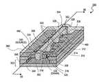
- Tri-gate transistor 300is formed on an substrate 302 .
- substrate 302is an insulating substrate which includes a lower monocrystalline silicon substrate 304 upon which is formed in insulating layer 306 , such as a silicon dioxide film.
- Tri-gate transistor 300can be formed on any well-known insulating substrate such as substrates formed from silicon dioxide, nitrides, oxides, and sapphires.
- the substrate 302can be a semiconductor substrate, such as but not limited to monocrystalline silicon substrate and gallium arsenide substrate.
- Tri-gate transistor 300includes a semiconductor body 308 and typically a plurality of semiconductor bodies 308 formed on insulator 306 of insulating substrate 302 .
- Semiconductor body 308can be formed of any well-known semiconductor material in which carrier mobility can be enhanced by applying a stress to the semiconductor, such as but not limited to silicon (Si) and silicon germanium (Si x Ge y ) where the Ge content is less than about 25%.
- a stresssuch as but not limited to silicon (Si) and silicon germanium (Si x Ge y ) where the Ge content is less than about 25%.
- Three-five (III-V) semiconductorssuch as gallium arsenide (GaAs), InSb, GaP, and GaSb may also benefit from applying a stress to them. It is thought that direct band gap materials may not benefit from applying a stress thereto, while non-direct band gaps will benefit.
- Semiconductor body 308is formed of a material which can be reversibly altered from an insulating state to a conductive state by applying external electrical controls.
- Semiconductor body 308is ideally a single crystalline film when the best electrical performance of transistor 300 , is desired.
- semiconductor body 308is a single crystalline film when transistor 300 is used in high performance applications, such as in a high density circuit, such as a microprocessor.
- Semiconductor body 308can be a polycrystalline film when transistor 300 is used in applications requiring less stringent performance, such as in liquid crystal displays.
- Insulator 306insulates semiconductor body 308 from monocrystalline silicon substrate 304 .
- semiconductor body 308is a single crystalline silicon film.
- Each semiconductor body or bodies 308has a pair of laterally opposite sidewalls 310 and 312 separated by a distance which defines a semiconductor body width 314 . Additionally, each semiconductor body 308 has a top surface 316 opposite a bottom surface 318 formed on substrate 302 . The distance between the top surface 316 and the bottom surface 318 defines a body height 320 . In an embodiment of the present invention the body height 320 is substantially equal to the body width 314 . In an embodiment of the present invention, the body 308 has a width 314 and height 320 less than 30 nanometers and ideally less than 20 nanometers. In an embodiment of the present invention, the body height 320 is between 1 ⁇ 2 the body width 314 to 2 times the body width 314 .
- Tri-gate transistor 300has a gate dielectric layer 322 .
- Gate dielectric layer 322is formed on and around three sides of each of the semiconductor bodies 308 as shown in FIGS. 3A and 3B .
- Gate dielectric layer 322is formed on or adjacent to sidewall 312 , on top surface 316 and on or adjacent to sidewall 310 of body 308 as shown in FIG. 3 .
- Gate dielectric layer 322can be any well-known gate dielectric layer.
- the gate dielectric layeris a silicon dioxide (SiO 2 ), silicon oxynitride (SiO x N y ) or a silicon nitride (Si 3 N 4 ) dielectric layer.
- the gate dielectric layer 322is a silicon oxynitride film formed to a thickness of between 5-20 ⁇ .
- gate dielectric layer 322is a high K gate dielectric layer, such as a metal oxide dielectric, such as but not limited to tantalum pentaoxide (Ta 2 O 5 ), titantium oxide (TiO 2 ), hafnium oxide (HfO 2 ), HfSiO x N y , zirconium oxide (ZrO 2 ) and lanthanum oxide LaO 2 ).
- Gate dielectric layer 322can be other types of high K dielectricS, such as but not limited to PZT.
- Tri-gate device 300has a gate electrode 324 .
- Gate electrode 324is formed on and around gate dielectric layer 322 as shown in FIGS. 3A and 3B .
- Gate electrode 324is formed on or adjacent to gate dielectric 322 formed on sidewall 312 of semiconductor body 308 , is formed on gate dielectric 322 formed on the top surface 316 of semiconductor body 308 , and is formed adjacent to or on gate dielectric layer 322 formed on sidewall 310 of semiconductor body 308 .
- Gate electrode 324has a pair of laterally opposite sidewalls 326 and 328 separated by a distance which defines the gate length (Lg) of transistor 300 .
- the laterally opposite sidewalls 326 and 328 of the gate electrode 324run in a direction perpendicular to the laterally opposite sidewalls 310 and 312 of semiconductor body 308 .
- Gate electrode 324can be formed of any suitable gate electrode material.
- to gate electrode 324comprises of polycrystalline silicon doped to a concentration density between 1 ⁇ 10 19 atoms/cm 3 -1 ⁇ 10 21 atoms/cm 3 .
- the gate electrodecan be a metal gate electrode, such as but not limited to, tungsten, tantalum, titanium, and their nitrides or alloys of various metallic systems.
- the gate electrodeis formed from a material having a work function between 3.9-5.3 eV. It is to be appreciated, the gate electrode 324 need not necessarily be a single material and can be a composite stack of thin films, such as but not limited to a polycrystalline silicon/metal electrode or a metal/polycrystalline silicon electrode.
- Tri-gate transistor 300has a source region 330 and a drain region 332 .
- Source region 330 and drain region 332are formed in semiconductor body 308 on opposite sides of gate electrode 324 as shown in FIG. 3A .
- the source region 330 and the drain region 332are formed of the same conductivity type such as N-type or P-type conductivity.
- source region 330 and drain region 332have a doping concentration of between 1 ⁇ 10 19 and 1 ⁇ 10 21 atoms/cm 3 .
- Source region 330 and drain region 332can be formed of uniform concentration or can include subregions of different concentrations or doping profiles such as tip regions (e.g., source/drain extensions).
- transistor 300when transistor 300 is a symmetrical transistor, source region 330 and drain region 332 will have the same doping concentration and profile. In an embodiment of the present invention when tri-gate transistor 300 is formed as an asymmetric transistor then the doping concentration and profile of the source region 330 and the drain region 332 may vary in order to obtain a particular electrical characteristic.
- the portion of semiconductor body 308 located between source region 330 and drain region 332defines the channel region 350 of transistor 300 .
- the channel region 350can also be defined as the area of the semiconductor body 308 surrounded by the gate electrode 324 .
- the source/drain regionmay extend slightly beneath the gate electrode through, for example, diffusion to define a channel region slightly smaller than the gate electrode length (Lg).
- channel region 350is intrinsic or undoped monocrystalline silicon.
- channel region 350is doped monocrystalline silicon. When channel region 350 is doped it is typically doped to a conductivity level of between 1 ⁇ 10 16 to 1 ⁇ 10 19 atoms/cm3.
- channel regionwhen the channel region is doped it is typically doped to the opposite conductivity type of the source region 330 and the drain region 332 .
- the channel regionwhen the source and drain regions are N-type conductivity the channel region would be doped to p type conductivity.
- the source and drain regionsare P type conductivity the channel region would be N-type conductivity.
- Channel region 350can be uniformly doped or can be doped non-uniformly or with differing concentrations to provide particular electrical and performance characteristics.
- channel regions 350can include well-known “halo” regions, if desired.
- the tri-gate transistoris characterized in having three channels and three gates, one (g 1 ) which extends between the source and drain regions on side 312 of silicon body 308 , a second (g 2 ) which extends between the source and drain regions on the top surface 316 of silicon body 308 , and the third (g 3 ) which extends between the source and drain regions on the sidewall 310 of silicon body 308 as shown in FIG. 3A and FIG. 3B .
- the gate “width” (Gw) of transistor 300is the sum of the widths of the three channel regions.
- the gate width of transistor 300is equal to the height 320 of silicon body 308 at sidewall 310 , plus the width of silicon body of 308 at the top surface 316 , plus the height 320 of silicon body 308 at sidewall 312 .
- Larger “width” transistorscan be obtained by using multiple devices coupled together (e.g., multiple silicon bodies 308 surrounded by a single gate electrode 324 as shown in FIG. 3A ).
- transistor 300can include an additional or multiple semiconductor bodies or fingers 308 as shown in FIG. 3A .
- Each semiconductor body 308has a gate dielectric layer 322 formed on its top surface and sidewalls as shown in FIG. 3A and FIG. 3B .
- Gate electrode 324is formed on and adjacent to each gate dielectric 322 on each of the semiconductor bodies 308 .
- Each semiconductor body 308also includes a source region 330 and a drain region 332 formed in the semiconductor body 308 on opposite sides of gate electrode 324 as shown in FIG. 3A .
- each semiconductor body 308is formed with the same width and height (thickness) as the other semiconductor bodies 308 .
- each source regions 330 and drain regions 332 of the semiconductor bodies 308are electrically coupled together by the semiconductor material used to form semiconductor body 308 to form a source landing pad 460 and a drain landing pad 480 as shown in FIG. 3A .
- the source regions 330 and drain regions 332can be coupled together by higher levels of metalization (e.g., metal 1 , metal 2 , metal 3 . . . ) used to electrically interconnect various transistors 300 together into functional circuits.
- the gate width of transistor 300 as shown in FIG. 3Awould be equal to the sum of the gate width created by each of the semiconductor bodies 308 . In this way, the tri-gate transistor 300 can be formed with any gate width desired.
- the tri-gate device of the present inventionincludes a film 360 which imparts a stress to the channel region 350 of the device.
- the mobility of the carriers (i.e., electrons or holes) for the devicecan be increased and the device performance improved.
- stress incorporating film 360is formed on and around exposed portions of semiconductor body 308 as shown in FIG. 3A and FIG. 3B . Additionally, in an embodiment of the present invention, the stress incorporating film 360 is formed over and around the gate electrode 324 .
- the stress incorporating film 360is formed directly on exposed top portion 322 of silicon body 308 as well as directly on or adjacent to sides 310 and 312 of semiconductor body 360 . Additionally, in an embodiment of the present invention, the stress incorporating film 360 is also formed directly on and adjacent to gate electrode 324 .
- the stress incorporating film 360is also formed directly beneath the bottom surface 318 of semiconductor body 308 including beneath the channel region 350 of the semiconductor body 308 as shown in FIG. 3A and FIG. 3B .
- the stress incorporating filmcan be formed beneath the semiconductor body or bodies by first removing a portion of the barried oxide or insulator 306 beneath the semiconductor body and then back filling the region with a stress incorporating film.
- the stress material 360completely surrounds the channel and provides stress from all side of the channel and not just the top.
- the film 360has a compressive stress so that the semiconductor body and especially the channel region of the semiconductor body is under a tensile stress.
- a channel region under a tensile stressimproves the mobility of electrons and therefore is ideal for use in a NMOS device where the carriers are electrons.
- the stress incorporating film 360is a film having suitable compressive stress to produce a tensile stress between 0.5-5.0 GPa and ideally about 1 GPa in the channel region of the semiconductor body.
- the stress incorporating film 360has a thickness between 10-200 nanometers.
- the stress film 360improves carrier mobility by 20-80 percent.
- the film 360has a tensile stress so that the semiconductor body 308 and especially the channel region 350 of the semiconductor body is under a compressive stress.
- a channel region under a compressive stressimproves the mobility of holes and therefore is ideal for use in a PMOS device where the carriers are holes.
- the film 360is a film having a suitable tensile stress to produce a compressive stress between 0.5-5.0 GPa in the channel region of the silicon body 308 .
- the thin film 360is a silicon nitride film having a tensile stress.
- a thin oxide or passivating film 319is formed on the underside 318 of the semiconductor bodies in order to help reduce parasitic leakage effects.
- the passivating film 319includes SiO 2 and can be formed to a thickness greater than about 1 nanometer.
- transistor 300can be operated in a fully depleted manner wherein when transistor 300 is turned “on” the channel region 350 fully depletes thereby providing the advantageous electrical characteristics and performance of a fully depleted transistor. That is, when transistor 300 is turned “ON” a depletion region is formed in channel region 350 along with an inversion layer at the surfaces of region 350 (i.e., an inversion layer is formed on the side surfaces and top surface of the semiconductor body).
- the inversion layerhas the same conductivity type as the source and drain regions and forms a conductive channel between the source and drain regions to allow current to flow therebetween.
- the depletion regiondepletes free carriers from beneath the inversion layer.
- the depletion regionextends to the bottom of channel region 350 , thus the transistor can be said to be a “fully depleted” transistor.
- Fully depleted transistorshave improved electrical performance characteristics over non-fully depleted or partially depleted transistors. For example, operating transistor 300 in a fully depleted manner, gives transistor 300 an ideal or very steep subthreshold slope.
- the tri-gate transistorcan be fabricated with very steep sub-threshold slope of less than 80 mV/decade, and ideally about 60 mV/decade even when fabricated with semiconductor body thicknesses of less than 30 nm.
- transistor 300has an improved drain induced barrier (DIBL) low in effect which provides for better “OFF” state leakage which results in lower leakage and thereby lower power consumption.
- DIBLdrain induced barrier
- the tri-gate transistor 300has a DIBL effect of less than 100 mV/V and ideally less than 40 mV/V.
- FIG. 6is an illustration of two plots 602 and 604 which set forth the body height and body width which will produce either fully depleted (F.D) or partially depleted (P.D) tri-gate transistors having gate length (Lg) of 30 nm ( 602 ) and 20 nm ( 604 ) respectively.
- the body height, body width and gate lengthare chosen to have dimensions in which a fully depleted transistor will be formed.
- the tri-gate transistorhas a body height, body width and gate length such that a partially depleted transistor is formed.
- the tri-gate transistor of the present inventioncan be said to be a non-planar transistor because the inversion layer of the channel region 350 is formed in both the horizontal and vertical directions in semiconductor body 308 .
- the semiconductor device of the present inventioncan also be considered a non-planar device because the electric field from the gate electrode 324 is applied from both horizontal (g 2 ) and vertical sides (g 1 and g 3 ).
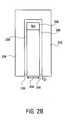
- tri-gate transistor 300can include other films or features, such as a silicon or other semiconductor film 410 , sidewall spacer 420 and silicide 430 formed prior to forming the stress incorporating film 360 as shown in FIG. 4 .
- a semiconductor film 410is formed on the source region 330 and on the drain region 332 of semiconductor body 308 to form “raised” source and drain regions.
- Semiconductor film 410can be a silicon film or a silicon alloy such as silicon germanium (Si x Ge y ).
- the semiconductor film 410is a single crystalline silicon film formed of the same conductivity type as the source region 330 and drain region 332 .
- the semiconductor filmcan be a silicon alloy such as silicon germanium wherein silicon comprises approximately 1 to 99 atomic percent of the alloy.
- the semiconductor film 410need not necessarily be a single crystalline semiconductor film and in an embodiment can be a polycrystalline film.
- Semiconductor film 410can be electrically isolated from a gate electrode 324 by a pair of dielectric sidewall spacers 420 such as silicon nitride or silicon oxide or composites thereof. Sidewall spacers 420 run along the laterally opposite sidewalls 326 and 328 of gate electrode 324 as shown in FIG. 4 thereby isolating the semiconductor film 410 from gate electrode 324 as shown in FIG. 4 .
- sidewalls spacers 420have a thickness of between 20-200 ⁇ .
- a suicide film 430such as, but not limited to, titanium silicide, nickel silicide, and cobalt silicide is formed on the source region 330 and drain region 332 .
- silicide film 430is formed on a silicon film 410 of silicon body 308 as shown in FIG. 4 .
- Silicide film 430can also be formed directly onto the top surface 316 of silicon body 308 .
- silicide film 430can be formed on silicon body 308 by first forming a silicon film such as an undoped silicon film and a silicon body and then completely consuming the silicon film during the silicide process.
- Dielectric spacers 420enable silicide film 430 to be formed on semiconductor body 308 or silicon film 410 in a self-aligned process (i.e., a salicide process).
- a semiconductor or silicon film 440can also be formed on the top of gate electrode 324 as can a silicide film 450 .
- Silicide film 450 and silicon film 440are typically formed at the same time as silicide film 430 and silicon film 410 on silicon body 308 .
- the formation of a silicon film 440 on silicide film 450 on the gate electrodereduces the contact resistance to the gate thereby improving the electrical performance of transistor 300 .
- FIGS. 5A-5EA method of fabricating a tri-gate transistor in accordance with embodiments of the present invention is illustrated in FIGS. 5A-5E .
- the fabrication of a tri-gate transistorbegins with substrate 502 .
- a silicon or semiconductor film 508is formed on substrate 502 as shown in FIG. 5A .
- the substrate 502is an insulating substrate, such as shown in FIG. 5A .
- insulating substrate 502includes a lower monocrystalline silicon substrate 504 and a top insulating layer 506 , such as a silicon dioxide film or silicon nitride film. Insulating layer 506 isolates semiconductor film 508 from substrate 504 , and in an embodiment is formed to a thickness between 200-2000 ⁇ .
- Insulating layer 506is sometimes referred to as a “buried oxide” layer.
- a silicon or semiconductor film 508is formed on an insulating substrate 502 , a silicon or semiconductor on insulating (SOI) substrate 500 is created.
- the substrate 502can be a semiconductor substrate, such as but not limited to a silicon monocrystalline substrate and a gallium arsenide substrate.
- semiconductor film 508is ideally a silicon film, in other embodiments it can be other types of semiconductor films in which carrier mobility can be enhanced when under stress, such as but not limited to a silicon germanium alloy (Si x Ge y ) with less than 25% Ge, and III-V materials such as, gallium arsenide (GaAs), InSb, GaP and GaSb.
- semiconductor film 508is an intrinsic (i.e., undoped) silicon film.
- semiconductor film 508is doped to a p type or n type conductivity with a concentration level between 1 ⁇ 10 16 -1 ⁇ 10 19 atoms/cm 3 .
- Semiconductor film 508can be insitu doped (i.e., doped while it is deposited) or doped after it is formed on substrate 502 by for example ion-implantation. Doping after formation enables both PMOS and NMOS tri-gate devices to be fabricated easily on the same insulating substrate. The doping level of the semiconductor body at this point determines the doping level of the channel region of the device.
- Semiconductor film 508is formed to a thickness which is approximately equal to the height desired for the subsequently formed semiconductor body or bodies of the fabricated tri-gate transistor. In an embodiment of the present invention, semiconductor film 508 has a thickness or height 509 of less than 30 nanometers and ideally less than 20 nanometers. In an embodiment of the present invention, semiconductor film 508 is formed to the thickness approximately equal to the gate “length” desired of the fabricated tri-gate transistor. In an embodiment of the present invention, semiconductor film 508 is formed thicker than desired gate length of the device. In an embodiment of the present invention, semiconductor film 508 is formed to a thickness which will enable the fabricated tri-gate transistor to be operated in a fully depleted manner for its designed gate length (Lg).
- Lggate length
- Semiconductor film 508can be formed on insulating substrate 502 in any well-known method.
- a silicon on insulator substrateknown as the SIMOX technique
- oxygen atomsare implanted at a high dose into a single crystalline silicon substrate and then annealed to form the buried oxide 506 within the substrate.
- the portion of the single crystalline silicon substrate above the buried oxidebecomes the silicon film 508 .
- Another technique currently used to form SOI substratesis an epitaxial silicon film transfer technique which is generally referred to as bonded SOI.
- bonded SOIIn this technique a first silicon wafer has a thin oxide grown on its surface that will later serve as the buried oxide 506 in the SOI structure.
- a high dose hydrogen implantis made into the first silicon wafer to form a high stress region below the silicon surface of the first wafer.
- This first Waferis then flipped over and bonded to the surface of a second silicon wafer.
- the first waferis then cleaved along the high stress plain created by the hydrogen implant. This results in a SOI structure with a thin silicon layer on top, the buried oxide underneath all on top of the single crystalline silicon substrate.
- Well-known smoothing techniquessuch as HC smoothing or chemical mechanical polishing (CMP) can be used to smooth the top surface of semiconductor film 508 to its desired thickness.
- isolation regionscan be formed into SOI substrate 502 in order to isolate the various transistors to be formed therein from one another. Isolation regions can be formed by etching away portions of the substrate film 508 surrounding a tri-gate transistor, by for example well-known photolithographic and etching techniques, and then back filling the etched regions with an insulating film, such as SiO 2 .
- the fins or bodies 520are patterned to have a width 518 which is equal to or greater than the width desired of the gate length (Lg) of the fabricated transistor. In this way, the most stringent photolithography constraints used to fabricate the transistor are associated with the gate electrode patterning and not the semiconductor body or fin definition.
- the semiconductor bodies or finswill have a width 518 less than or equal to 30 nanometers and ideally less than or equal to 20 nanometers.
- the semiconductor bodies or finshave a width 518 approximately equal to the silicon body height 509 .
- the fins or bodies 520have a width 518 which is between 1 ⁇ 2 the semiconductor body height 509 and two times the semiconductor body height 509 .
- the photolithography and etching stepcan also be used to form source landing pads 522 and drain landing pads 524 from the semiconductor film.
- the landing padscan be used to connect together the various source regions and to connect together the various drain regions of the fabricated transistor.
- the semicoductor film 508can be patterned into fins and landing pads utilizing well known photolithography and etching techniques which generally include the formation of a photoresist mask by masking, exposing, and developing a blanket deposited photoresist film as is well known in the art, and then etching semiconductor film in alignment with the photoresist mask to form one or more silicon bodies or fins 520 and source and drain landing pads 522 and 524 respectively.
- Semiconductor film 508is etched until the underlying buried oxide layer 506 is exposed.
- Well-known semiconductor etching techniquessuch as anisotropic plasma etching or reactive ion etching can be used to etch semiconductor film 508 in alignment with the photoresist mask.
- semiconductor film 508is etched to form semiconductor bodies or fins 520 (and source/drain landing pads 522 and 524 , if desired)
- the photoresist maskis removed by well-known techniques, such as by chemical stripping and O2 ashing, to produce the substrate shown in FIG. 5B .
- a gate dielectric layer 526is formed on and around each semiconductor body 520 . That is, a gate dielectric layer 526 is formed on the top surface 527 of each of the semiconductor bodies 520 as well as on the laterally opposite sidewalls 528 and 529 of each of the semiconductor bodies 520 .
- the gate dielectriccan be a deposited dielectric or a grown dielectric.
- the gate dielectric layer 526is a silicon dioxide dielectric film grown with a dry/wet oxidation process. In an embodiment of the present invention, the silicon oxide film is grown to a thickness of between 5-15 ⁇ .
- the gate dielectric film 526is a deposited dielectric, such as but not limited to a high dielectric constant film, such as metal oxide dielectric, such as tantalum pentaoxide (Ta 2 O 5 ), titanium oxide (TiO 2 ), hafnium oxide (HfO 2 ), HfSiO x N y , zirconium oxide (ZrO 2 ) and lanthanum oxide LaO 2 ) or other high-K dielectrics, such as PZT and BST.
- a high dielectric constant filmcan be formed by any well-known technique, such as by chemical vapor deposition (CVD).
- a gate electrode 530is formed.
- the gate electrode 530is formed on the gate dielectric layer 526 formed on the top surface 527 of each of the semiconductor bodies 520 and is formed on or adjacent to the gate dielectric 526 formed on or adjacent to the sidewalls 528 and 529 of each of the semiconductor bodies as shown in FIG. 5E .
- the gate electrode 530has a top surface 532 opposite of bottom surface formed on the insulating substrate 502 and has a pair of laterally opposite sidewalls 534 and 536 . The distance between the laterally opposite sidewalls 534 and 536 defines the gate length (Lg) 538 of the tri-gate transistor.
- Gate electrode 530can be formed by blanket depositing a suitable gate electrode material over the substrate and then patterning the material into an electrode 530 .
- the gate electrodecan be formed to a thickness 533 between 200-3000 ⁇ . In an embodiment the gate electrode has a thickness or height 533 of at least three times the height 509 of semiconductor bodies 520 .
- the gate electrode materialis then patterned with well-known photolithography and etching techniques to form gate electrode 530 from the gate electrode material.
- the gate electrode materialcomprises polycrystalline silicon.
- the gate electrode materialcomprises a polycrystalline silicon germanium alloy.
- the gate electrode materialcan comprise a metal film, such as tungsten, tantalum, and their nitrides.
- Gate electrode 530can be formed by well-known techniques, such as by blanket depositing a gate electrode material over the substrate of FIG. 5B and then patterning the gate electrode material with well-known photolithography and etching techniques.
- the photolithography process used to define gate electrode 530utilizes the minimum or smallest dimension lithography process used to fabricate the tri-gate transistor. (That is, in an embodiment of the present invention, the gate length (Lg) 538 of gate electrode 530 has a minimum feature dimension of the transistor defined by photolithography.)
- the gate length 538is less than or equal to 30 nanometers and ideally less than or equal to 20 nanometers.
- source and drain regions for the transistorare formed in semiconductor body 520 on opposite sides of gate electrode 530 .
- the source and drain regionsinclude tip or source/drain extension regions.
- Source and drain extension regions 540 and 542can be formed by placing dopants 544 into semiconductor bodies 520 on both sides 532 , 534 of gate electrode 530 in order to form tip regions 540 and 542 as shown in FIG. 5D .
- the semiconductor fins or bodies 520are doped to a p type conductivity and to a concentration between 1 ⁇ 10 20 -1 ⁇ 10 21 atoms/cm 3 .
- the semiconductor fins or bodies 520is doped with n type conductivity ions to a concentration between 1 ⁇ 10 20 -1 ⁇ 10 21 atoms/cm 3 .
- the silicon filmsare doped by ion-implantation.
- the ion-implantationoccurs in a vertical direction (i.e., a direction perpendicular to substrate 502 ).
- gate electrode 530is a polysilicon gate electrode, it can be doped during the ion-implantation process. Gate electrode 530 acts as a mask to prevent the ion-implantation step from doping the channel region(s) 548 of the tri-gate transistor.
- the channel region 548is the portion of the silicon body 520 located beneath or surrounded by the gate electrode 530 .
- gate electrode 530is a metal electrode, a dielectric hard mask maybe used to block the doping during the ion-implantation process. In other embodiments, other methods, such as solid source diffusion, may be used to dope the semiconductor body to form source and drain extensions.
- Halo regionscan be formed in the silicon body prior to the formation of source/drain regions or source/drain extension regions.
- Halo regionsare doped regions formed in the channel region 548 of the device and are of the same conductivity but of a slightly higher concentration than the doping of the channel region of the device.
- Halo regionscan be formed by ion-implanting dopants beneath the gate electrode by utilizing large angled ion-implantation techniques.
- the substrate shown in FIG. 5Ccan be further processed to form additional features, such as heavily doped source/drain contact regions, deposited silicon on the source and drain regions to form raised source and drain regions, as well as the gate electrode, and the formation of silicide on the source/drain contact regions as well as on the gate electrode.
- additional featuressuch as heavily doped source/drain contact regions, deposited silicon on the source and drain regions to form raised source and drain regions, as well as the gate electrode, and the formation of silicide on the source/drain contact regions as well as on the gate electrode.
- the buried oxide layer 506 located underneath and adjacent to the semiconductor fins or bodiesis removed to form an air gap 560 in the buried oxide layer.
- the buried oxide layercan be removed by using a selective etch which preferencely etches the buried insulating film without substantially etching away the semiconductor body.
- the semiconductor bodiesare silicon and the buried insulating layer 506 is a silicon oxide
- the buried silicon oxide layercan be selectively etched away with a buffered HF etchant. It is to be appreciated that any suitable wet or dry etch technique which can selectively etch away the buried insulating layer without etching away the semiconductor body may be utilized to form air gaps 560 .
- An etchant with a selectivity of greater than 10is desirable.
- the buried insulator etchcan be performed on the wafer with or without a patterning layer depending upon the layout of the device. Typically a patterned photoresist mask will be utilized which exposes the transistors which are to receive the subsequent stress film and covers those transistors which are not to include a stress film.
- a short oxidation or passivation stepcan be performed to passivate the bottom of the exposed fins in order to reduce parasitic leakeage effects. Any suitable oxidation or passivation process can be used to form the passivating dielectric.
- the bottom of the finsare passivated by SiO 2 to form a passivating oxide film having a thickness greater than about 1 nanometer.
- the stress incorporation film 560must be an insulating film in order to prevent shorts from the source to the drain.
- the purpose of the stress incorporation filmis to provide stress in the channel region of the device.
- the type of stress in the stress incorporation filmdepends upon the type of device being fabricated. For a NMOS device where the carriers are electrons, the channel regions need to be under tensile stress to increase mobility of electrons. In order to place the channel region under tensile stress, the stress incorporation film 560 needs to be a compressive film.
- the process used to form the stress incorporation film 560should be a conformal process, such as a vapor phase deposition, which can blanket deposit the film equally on vertical and horizontal surfaces and be able to fill underneath the semiconductor bodies. It is desirable that the stress incorporation film be able to completely fill the regions underneath the fins or bodies of the device. This can be facilitated by making narrower fins or making the underlying insulating film layer 506 thicker in order to improve the aspect ratio of the fill under the channel regions.
- the stress incorporation filmis a compressive silicon nitride film.
- an NMOS deviceis fabricated with a compressive silicon nitride film formed by chemical vapor deposition (CVD) utilizing a reactant gas mixture comprising dichloro-silane (DCS) and ammonia (NH 3 ).
- DCSdichloro-silane
- NH 3ammonia
- BTBAScan also be used in place of DCS.
- Such a processwill blanket deposit a silicon nitride film over the substrate with equal deposition on horizontal and vertical surfaces and enable the filling of the air gap beneath the silicon bodies.
- the channel regionsneeds to be in compression to increase the mobility of the holes.
- the stress incorporation filmneeds to be a tensile film.
- the stress incorporation filmis a tensile silicon nitride film.
- the stress incorporation filmis formed to a thickness sufficient to completely fill the air gap regions beneath the semiconductor bodies and channel region and completely surround the semiconductor body and gate electrode as shown in FIG. 5E .
- the stress incorporation filmcompletely surrounds the device and provides stress over a large area resulting in the desired stress in the channel to improve mobility.
- the film stress propertiesare modulated during deposition in order to optimize the film for device performance.
- a masking and etch stepcan be used to remove the stress incorporation film from areas where it is not desired, and processing continued in a normal manner to form “back end” features, such as metal interconnects and interlayer dielectrics to electrically couple the individual transistors together into a functional circuit.
Landscapes
- Engineering & Computer Science (AREA)
- Physics & Mathematics (AREA)
- Condensed Matter Physics & Semiconductors (AREA)
- General Physics & Mathematics (AREA)
- Manufacturing & Machinery (AREA)
- Computer Hardware Design (AREA)
- Microelectronics & Electronic Packaging (AREA)
- Power Engineering (AREA)
- Thin Film Transistor (AREA)
- Insulated Gate Type Field-Effect Transistor (AREA)
- Metal-Oxide And Bipolar Metal-Oxide Semiconductor Integrated Circuits (AREA)
Abstract
Description
- This is a Divisional Application of, and claims priority to, Ser. No. 11/173,443 filed on Jun. 30, 2005, which is a Continuation Application of, and claims priority to, Ser. No. 10/834,717 filed on Apr. 28, 2004, which issued on Dec. 13, 2005 as U.S. Pat. No. 6,974,738 and which is a Divisional Application of, and claims priority to, Ser. No. 10/607,632 filed on Jun. 27, 2003, which was issued on Jun. 21, 2005 as U.S. Pat. No. 6,909,151.
- 1. Field of the Invention
- The present invention relates to the field of semiconductor integrated circuit manufacturing and more specifically to a non-planar transistor having stress incorporation layer.
- 2. Discussion of Related Art
- In order to increase device performance, silicon on insulator (SOI) transistors have been proposed for the fabrication of modern integrated circuits.
FIG. 1 illustrates a standard fully depleted silicon on insulator (SOI)transistor 100.SOI transistor 100 includes a singlecrystalline silicon substrate 102 having aninsulating layer 104, such as a buried oxide formed thereon. A singlecrystalline silicon body 106 is formed on theinsulating layer 104. A gatedielectric layer 108 is formed on the singlecrystalline silicon body 106 and agate electrode 110 formed on the gate dielectric108.Source 112 anddrain 114 regions are formed in thesilicon body 106 along laterally opposite sides ofgate electrode 110. - Fully depleted SOI have been proposed as a transistor structure to take advantage of ideal sub-threshold gradients for optimized on current/off current ratios. In order to achieve ideal subthreshold gradients with
transistor 100, the thickness of thesilicon body 106 must be about ⅓ the size of the gate length (Lg) of the transistor or Tsi=Lg/3. However, as gate lengths scale especially as they approach 30 nm, the need for ever decreasing silicon film thickness (Tsi) makes this approach increasingly impractical. At 30 nanometer gate length, the thickness required of the silicon body is thought to need to be less than 10 nanometers, and around 6 nanometer for a 20 nanometer gate length. The fabrication of thin silicon films with thicknesses of less than 10 nanometers, is considered to be extremely difficult. On one hand, obtaining wafer uniformity on the order of one nanometer is a difficult challenge. On the other hand, to be able to contact these thin films to form raised source/drain regions to decrease junction resistance, becomes almost impossible since the thin silicon layer in the source/drain regions becomes consumed during the gate etch and various cleans following the gate etch and spacer etch leavinginsufficient silicon 106 for silicon to grow on. - A double gate (DG) device, such as shown in
FIGS. 2A and 2B , have been proposed to alleviate the silicon thickness issue. The double gate (DG)device 200 includes asilicon body 202 formed on aninsulating substrate 204. A gate dielectric206 is formed on two sides of thesilicon body 202 and agate electrode 208 is formed adjacent to the gate dielectric206 formed on the two sides of thesilicon body 202. A sufficiently thickinsulating layer 209, such as silicon nitride, electrically isolates thegate electrode 208 from the top ofsilicon body 202. - Double gate (DG)
device 200 essentially has two gates, one on either side of the channel of the device. Because thedouble gate device 200 has a gate on each side of the channel, thickness (Tsi) of the silicon body can be double that of a single gate device and still obtain a fully depleted transistor operation. That is, with a double gate device200 a fully depleted transistor can be formed where Tsi=(2×Lg)/3. The most manufacturable form of the double gate (DG)device 200, however, requires that thebody 202 patterning be done with photolithography that is 0.7× smaller than that used to pattern the gate length (Lg) of the device. In order to obtain high density integrated circuits, it is generally desirable to have the most aggressive lithography occur with respect to the gate length (Lg) of thegate electrode 208. Although, double gate structures double the thickness of the silicon film (since there now is a gate on either side of the channel) these structures, however, are hideously difficult to fabricate. For example,silicon body 202 requires a silicon body etch which can produce asilicon body 202 with an aspect ratio (height to width) of about 5:1. FIG. 1 is an illustration of a cross-sectional view of a depleted substrate transitor.FIGS. 2A and 2B illustrate a double gate depleted substrate transistor.FIGS. 3A and 3B is an illustration of a tri-gate transistor having a stress incorporation film in accordance with the present invention.FIG. 4 is an illustration of a tri-gate transistor in accordance with an embodiment of the present invention.FIGS. 5A-5E illustrate methods of fabricating a tri-gate transistor with a stress incorporation film in accordance with embodiments of the present invention.FIG. 6 is a plot which illustrates body heights and body widths which can be used to obtain partially depleted and fully depleted tri-gate transistors having gate lengths (Lg) of 30 nm and 20 nm.- The present invention is a novel tri-gate or non-planar transistor structure with a stress incorporating layer and its method of fabrication. In the following description numerous specific details are set forth in order to provide a thorough understanding in the present invention. In other instances, well-known semiconductor process and manufacturing techniques have not been described in particular detail in order to not unnecessarily obscure the present invention.
- The present invention is novel non-planar or tri-gate transistor structure and its method of fabrication. The tri-gate transistor includes a stress film formed around the channel region of the device to provides a stress to the channel region to improve carrier mobility. Greater carrier mobility results in increased transistor drive current. In an embodiment of the present invention, the stress film is formed beneath the channel region so that it completely surrounds the channel. By completely surrounding the channel region with the stress film, the stress film provides stress to all sides of the channel, thereby providing stress over a large area and maximizing and improving device performance. The film stress properties, such a type of stress (i.e., compressive or tensile) and the amount of stress can be varied in order to optimize performance for different transistor types (e.g., PMOS and NMOS).
- In an embodiment of the present invention, the tri-gate transistor is a semiconductor on insulator (SOI) transistor. The tri-gate transistor is ideal for use in fully depleted substrate transistor applications. The tri-gate transistor includes a thin semiconductor body formed on an substrate, the substrate can be an insulating substrate or a semiconductor substrate. A gate dielectric is formed on the top surface and the sidewalls of the semiconductor body. A gate electrode is formed on the gate dielectric on the top surface of the semiconductor body and is formed adjacent to the gate dielectric formed on the sidewalls of the semiconductor body. Source and drain regions are formed in the semiconductor body on opposite sides of the gate electrode. Because the gate electrode and the gate dielectric surround the semiconductor body on three sides, the transistor essentially has three separate channels and gates. The gate “width” of a transistor is equal to the sum of each of the three sides of the semiconductor body. Larger “width” transistors can be formed by connecting several tri-gate transistors together.
- Because there are three separate channels formed in the semiconductor body, the semiconductor body can be fully depleted when the transistor is turned “ON”, thereby enabling the formation of a fully depleted transistor with gate lengths of less than 30 nanometers without requiring the use of ultra-thin semiconductor bodies or requiring photolithographic patterning of the semiconductor bodies to dimensions less than the gate length (Lg) of the device. That is, the structure of the tri-gate transistor of the present invention enables a fully depleted transistor to be fabricated where the thickness of the semiconductor body and width of the semiconductor body are equal to the gate length of the device. Because the novel tri-gate transistor of the present invention can be operated in a fully depleted manner, the device is characterized by ideal (i.e., very sharp) subthreshold slope and a reduced drain induced barrier lowering (DIBL) short channel effect of less than 100 mV/V and ideally about 60 mV/V which results in a lower leakage current when the device is turned “OFF” resulting in lower power consumption.
- An example of a
tri-gate transistor 300 with stress incorporation film in accordance with an embodiment of present invention as illustrated inFIGS. 3A and 3B . (FIG. 3B is a cross-sectional view ofFIG. 3A taken through thegate electrode 324 of one of thesemiconductor bodies 308.)Tri-gate transistor 300 is formed on ansubstrate 302. In an embodiment of the present invention,substrate 302 is an insulating substrate which includes a lowermonocrystalline silicon substrate 304 upon which is formed in insulatinglayer 306, such as a silicon dioxide film.Tri-gate transistor 300, however, can be formed on any well-known insulating substrate such as substrates formed from silicon dioxide, nitrides, oxides, and sapphires. In an embodiment of the present invention, thesubstrate 302 can be a semiconductor substrate, such as but not limited to monocrystalline silicon substrate and gallium arsenide substrate. Tri-gate transistor 300 includes asemiconductor body 308 and typically a plurality ofsemiconductor bodies 308 formed oninsulator 306 of insulatingsubstrate 302.Semiconductor body 308 can be formed of any well-known semiconductor material in which carrier mobility can be enhanced by applying a stress to the semiconductor, such as but not limited to silicon (Si) and silicon germanium (SixGey) where the Ge content is less than about 25%. Three-five (III-V) semiconductors, such as gallium arsenide (GaAs), InSb, GaP, and GaSb may also benefit from applying a stress to them. It is thought that direct band gap materials may not benefit from applying a stress thereto, while non-direct band gaps will benefit.Semiconductor body 308 is formed of a material which can be reversibly altered from an insulating state to a conductive state by applying external electrical controls.Semiconductor body 308 is ideally a single crystalline film when the best electrical performance oftransistor 300, is desired. For example,semiconductor body 308 is a single crystalline film whentransistor 300 is used in high performance applications, such as in a high density circuit, such as a microprocessor.Semiconductor body 308, however, can be a polycrystalline film whentransistor 300 is used in applications requiring less stringent performance, such as in liquid crystal displays.Insulator 306 insulatessemiconductor body 308 frommonocrystalline silicon substrate 304. In an embodiment of the present invention,semiconductor body 308 is a single crystalline silicon film. Each semiconductor body orbodies 308 has a pair of laterallyopposite sidewalls semiconductor body width 314. Additionally, eachsemiconductor body 308 has atop surface 316 opposite abottom surface 318 formed onsubstrate 302. The distance between thetop surface 316 and thebottom surface 318 defines abody height 320. In an embodiment of the present invention thebody height 320 is substantially equal to thebody width 314. In an embodiment of the present invention, thebody 308 has awidth 314 andheight 320 less than 30 nanometers and ideally less than 20 nanometers. In an embodiment of the present invention, thebody height 320 is between ½ thebody width 314 to 2 times thebody width 314.Tri-gate transistor 300 has agate dielectric layer 322.Gate dielectric layer 322 is formed on and around three sides of each of thesemiconductor bodies 308 as shown inFIGS. 3A and 3B .Gate dielectric layer 322 is formed on or adjacent to sidewall312, ontop surface 316 and on or adjacent to sidewall310 ofbody 308 as shown inFIG. 3 .Gate dielectric layer 322 can be any well-known gate dielectric layer. In an embodiment of the present invention, the gate dielectric layer is a silicon dioxide (SiO2), silicon oxynitride (SiOxNy) or a silicon nitride (Si3N4) dielectric layer. In an embodiment of the present invention, thegate dielectric layer 322 is a silicon oxynitride film formed to a thickness of between 5-20 Å. In an embodiment of the present invention,gate dielectric layer 322 is a high K gate dielectric layer, such as a metal oxide dielectric, such as but not limited to tantalum pentaoxide (Ta2O5), titantium oxide (TiO2), hafnium oxide (HfO2), HfSiOxNy, zirconium oxide (ZrO2) and lanthanum oxide LaO2).Gate dielectric layer 322 can be other types of high K dielectricS, such as but not limited to PZT.Tri-gate device 300 has agate electrode 324.Gate electrode 324 is formed on and aroundgate dielectric layer 322 as shown inFIGS. 3A and 3B .Gate electrode 324 is formed on or adjacent to gate dielectric322 formed onsidewall 312 ofsemiconductor body 308, is formed ongate dielectric 322 formed on thetop surface 316 ofsemiconductor body 308, and is formed adjacent to or ongate dielectric layer 322 formed onsidewall 310 ofsemiconductor body 308.Gate electrode 324 has a pair of laterallyopposite sidewalls transistor 300. In an embodiment of the present invention the laterally oppositesidewalls gate electrode 324 run in a direction perpendicular to the laterally oppositesidewalls semiconductor body 308.Gate electrode 324 can be formed of any suitable gate electrode material. In an embodiment of the present invention togate electrode 324 comprises of polycrystalline silicon doped to a concentration density between 1×10¹⁹atoms/cm3-1×1021atoms/cm3. In an embodiment of the present invention the gate electrode can be a metal gate electrode, such as but not limited to, tungsten, tantalum, titanium, and their nitrides or alloys of various metallic systems. In an embodiment of the present invention the gate electrode is formed from a material having a work function between 3.9-5.3 eV. It is to be appreciated, thegate electrode 324 need not necessarily be a single material and can be a composite stack of thin films, such as but not limited to a polycrystalline silicon/metal electrode or a metal/polycrystalline silicon electrode.Tri-gate transistor 300 has asource region 330 and adrain region 332.Source region 330 and drainregion 332 are formed insemiconductor body 308 on opposite sides ofgate electrode 324 as shown inFIG. 3A . Thesource region 330 and thedrain region 332 are formed of the same conductivity type such as N-type or P-type conductivity. In an embodiment of the presentinvention source region 330 and drainregion 332 have a doping concentration of between 1×10¹⁹and 1×10²¹atoms/cm3.Source region 330 and drainregion 332 can be formed of uniform concentration or can include subregions of different concentrations or doping profiles such as tip regions (e.g., source/drain extensions). In an embodiment of the present invention whentransistor 300 is a symmetrical transistor,source region 330 and drainregion 332 will have the same doping concentration and profile. In an embodiment of the present invention whentri-gate transistor 300 is formed as an asymmetric transistor then the doping concentration and profile of thesource region 330 and thedrain region 332 may vary in order to obtain a particular electrical characteristic.- The portion of
semiconductor body 308 located betweensource region 330 and drainregion 332, defines thechannel region 350 oftransistor 300. Thechannel region 350 can also be defined as the area of thesemiconductor body 308 surrounded by thegate electrode 324. At times however, the source/drain region may extend slightly beneath the gate electrode through, for example, diffusion to define a channel region slightly smaller than the gate electrode length (Lg). In an embodiment of the presentinvention channel region 350 is intrinsic or undoped monocrystalline silicon. In an embodiment of the present invention,channel region 350 is doped monocrystalline silicon. Whenchannel region 350 is doped it is typically doped to a conductivity level of between 1×10¹⁶to 1×10¹⁹atoms/cm3. In an embodiment of the present invention, when the channel region is doped it is typically doped to the opposite conductivity type of thesource region 330 and thedrain region 332. For example, when the source and drain regions are N-type conductivity the channel region would be doped to p type conductivity. Similarly, when the source and drain regions are P type conductivity the channel region would be N-type conductivity. In this manner atri-gate transistor 300 can be formed into either a NMOS transistor or a PMOS transistor respectively.Channel region 350 can be uniformly doped or can be doped non-uniformly or with differing concentrations to provide particular electrical and performance characteristics. For example,channel regions 350 can include well-known “halo” regions, if desired. - By providing a gate dielectric and a gate electrode which surrounds the semiconductor body on three sides, the tri-gate transistor is characterized in having three channels and three gates, one (g1) which extends between the source and drain regions on
side 312 ofsilicon body 308, a second (g2) which extends between the source and drain regions on thetop surface 316 ofsilicon body 308, and the third (g3) which extends between the source and drain regions on thesidewall 310 ofsilicon body 308 as shown inFIG. 3A andFIG. 3B . The gate “width” (Gw) oftransistor 300 is the sum of the widths of the three channel regions. That is, the gate width oftransistor 300 is equal to theheight 320 ofsilicon body 308 atsidewall 310, plus the width of silicon body of308 at thetop surface 316, plus theheight 320 ofsilicon body 308 atsidewall 312. Larger “width” transistors can be obtained by using multiple devices coupled together (e.g.,multiple silicon bodies 308 surrounded by asingle gate electrode 324 as shown inFIG. 3A ). - As stated above the gate “width” of
transistor 300 is equal to the sum of the three gate width created fromsemiconductor body 308 oftransistor 300. In order to fabricate the transistors with larger gate widths,transistor 300 can include an additional or multiple semiconductor bodies orfingers 308 as shown inFIG. 3A . Eachsemiconductor body 308 has agate dielectric layer 322 formed on its top surface and sidewalls as shown inFIG. 3A andFIG. 3B .Gate electrode 324 is formed on and adjacent to eachgate dielectric 322 on each of thesemiconductor bodies 308. Eachsemiconductor body 308 also includes asource region 330 and adrain region 332 formed in thesemiconductor body 308 on opposite sides ofgate electrode 324 as shown inFIG. 3A . In an embodiment of the present invention eachsemiconductor body 308 is formed with the same width and height (thickness) as theother semiconductor bodies 308. In an embodiment of the present invention eachsource regions 330 anddrain regions 332 of thesemiconductor bodies 308 are electrically coupled together by the semiconductor material used to formsemiconductor body 308 to form asource landing pad 460 and adrain landing pad 480 as shown inFIG. 3A . Alternatively, thesource regions 330 anddrain regions 332 can be coupled together by higher levels of metalization (e.g., metal1,metal 2,metal 3 . . . ) used to electrically interconnectvarious transistors 300 together into functional circuits. The gate width oftransistor 300 as shown inFIG. 3A would be equal to the sum of the gate width created by each of thesemiconductor bodies 308. In this way, thetri-gate transistor 300 can be formed with any gate width desired. - Additionally, as shown in
FIG. 3A andFIG. 3B , the tri-gate device of the present invention includes afilm 360 which imparts a stress to thechannel region 350 of the device. By applying a proper stress to the channel region, the mobility of the carriers (i.e., electrons or holes) for the device can be increased and the device performance improved. In an embodiment of the present invention,stress incorporating film 360 is formed on and around exposed portions ofsemiconductor body 308 as shown inFIG. 3A andFIG. 3B . Additionally, in an embodiment of the present invention, thestress incorporating film 360 is formed over and around thegate electrode 324. In an embodiment of the present invention, thestress incorporating film 360 is formed directly on exposedtop portion 322 ofsilicon body 308 as well as directly on or adjacent tosides semiconductor body 360. Additionally, in an embodiment of the present invention, thestress incorporating film 360 is also formed directly on and adjacent togate electrode 324. - Additionally, in an embodiment of the present invention, the
stress incorporating film 360 is also formed directly beneath thebottom surface 318 ofsemiconductor body 308 including beneath thechannel region 350 of thesemiconductor body 308 as shown inFIG. 3A andFIG. 3B . The stress incorporating film can be formed beneath the semiconductor body or bodies by first removing a portion of the barried oxide orinsulator 306 beneath the semiconductor body and then back filling the region with a stress incorporating film. By including a stress incorporating film directly beneath the bottom surface of thechannel region 350 ofsemiconductor bodies 308, thestress material 360 completely surrounds the channel and provides stress from all side of the channel and not just the top. - In an embodiment of the present invention, the
film 360 has a compressive stress so that the semiconductor body and especially the channel region of the semiconductor body is under a tensile stress. A channel region under a tensile stress improves the mobility of electrons and therefore is ideal for use in a NMOS device where the carriers are electrons. In an embodiment of the present invention, thestress incorporating film 360 is a film having suitable compressive stress to produce a tensile stress between 0.5-5.0 GPa and ideally about 1 GPa in the channel region of the semiconductor body. In an embodiment of the present invention, thestress incorporating film 360 has a thickness between 10-200 nanometers. In an embodiment of the present invention, thestress film 360 improves carrier mobility by 20-80 percent. - In an embodiment of the present invention, the
film 360 has a tensile stress so that thesemiconductor body 308 and especially thechannel region 350 of the semiconductor body is under a compressive stress. A channel region under a compressive stress improves the mobility of holes and therefore is ideal for use in a PMOS device where the carriers are holes. In an embodiment of the present invention, thefilm 360 is a film having a suitable tensile stress to produce a compressive stress between 0.5-5.0 GPa in the channel region of thesilicon body 308. In an embodiment of the present invention, thethin film 360 is a silicon nitride film having a tensile stress. - In an embodiment of the present invention, a thin oxide or
passivating film 319 is formed on theunderside 318 of the semiconductor bodies in order to help reduce parasitic leakage effects. In an embodiment of the present invention, thepassivating film 319 includes SiO2and can be formed to a thickness greater than about 1 nanometer. - Because the
channel region 350 is surrounded on three sides bygate electrode 324 andgate dielectric 322,transistor 300 can be operated in a fully depleted manner wherein whentransistor 300 is turned “on” thechannel region 350 fully depletes thereby providing the advantageous electrical characteristics and performance of a fully depleted transistor. That is, whentransistor 300 is turned “ON” a depletion region is formed inchannel region 350 along with an inversion layer at the surfaces of region350 (i.e., an inversion layer is formed on the side surfaces and top surface of the semiconductor body). The inversion layer has the same conductivity type as the source and drain regions and forms a conductive channel between the source and drain regions to allow current to flow therebetween. The depletion region depletes free carriers from beneath the inversion layer. The depletion region extends to the bottom ofchannel region 350, thus the transistor can be said to be a “fully depleted” transistor. Fully depleted transistors have improved electrical performance characteristics over non-fully depleted or partially depleted transistors. For example, operatingtransistor 300 in a fully depleted manner, givestransistor 300 an ideal or very steep subthreshold slope. The tri-gate transistor can be fabricated with very steep sub-threshold slope of less than 80 mV/decade, and ideally about 60 mV/decade even when fabricated with semiconductor body thicknesses of less than 30 nm. Additionally, operatingtransistor 300 in the fully depleted manner,transistor 300 has an improved drain induced barrier (DIBL) low in effect which provides for better “OFF” state leakage which results in lower leakage and thereby lower power consumption. In an embodiment of the present invention thetri-gate transistor 300 has a DIBL effect of less than 100 mV/V and ideally less than 40 mV/V. FIG. 6 is an illustration of twoplots - The tri-gate transistor of the present invention can be said to be a non-planar transistor because the inversion layer of the
channel region 350 is formed in both the horizontal and vertical directions insemiconductor body 308. The semiconductor device of the present invention can also be considered a non-planar device because the electric field from thegate electrode 324 is applied from both horizontal (g2) and vertical sides (g1 and g3). - In an embodiment of the present invention
tri-gate transistor 300 can include other films or features, such as a silicon orother semiconductor film 410,sidewall spacer 420 andsilicide 430 formed prior to forming thestress incorporating film 360 as shown inFIG. 4 . For example, in an embodiment of the present invention asemiconductor film 410 is formed on thesource region 330 and on thedrain region 332 ofsemiconductor body 308 to form “raised” source and drain regions.Semiconductor film 410 can be a silicon film or a silicon alloy such as silicon germanium (SixGey). In an embodiment of the present invention thesemiconductor film 410 is a single crystalline silicon film formed of the same conductivity type as thesource region 330 and drainregion 332. In an embodiment of the present invention the semiconductor film can be a silicon alloy such as silicon germanium wherein silicon comprises approximately 1 to 99 atomic percent of the alloy. Thesemiconductor film 410 need not necessarily be a single crystalline semiconductor film and in an embodiment can be a polycrystalline film.Semiconductor film 410 can be electrically isolated from agate electrode 324 by a pair ofdielectric sidewall spacers 420 such as silicon nitride or silicon oxide or composites thereof.Sidewall spacers 420 run along the laterally oppositesidewalls gate electrode 324 as shown inFIG. 4 thereby isolating thesemiconductor film 410 fromgate electrode 324 as shown inFIG. 4 . An embodiment of the presentinvention sidewalls spacers 420 have a thickness of between 20-200 Å. By adding a silicon or semiconductor film to the source and drainregions transistor 300 and improving its electrical characteristics and performance. - In an embodiment of the present invention a
suicide film 430, such as, but not limited to, titanium silicide, nickel silicide, and cobalt silicide is formed on thesource region 330 and drainregion 332. In an embodiment of the presentinvention silicide film 430 is formed on asilicon film 410 ofsilicon body 308 as shown inFIG. 4 .Silicide film 430 however can also be formed directly onto thetop surface 316 ofsilicon body 308. For example,silicide film 430 can be formed onsilicon body 308 by first forming a silicon film such as an undoped silicon film and a silicon body and then completely consuming the silicon film during the silicide process.Dielectric spacers 420 enablesilicide film 430 to be formed onsemiconductor body 308 orsilicon film 410 in a self-aligned process (i.e., a salicide process). - Additionally, in the embodiment of the present invention a semiconductor or
silicon film 440 can also be formed on the top ofgate electrode 324 as can asilicide film 450.Silicide film 450 andsilicon film 440 are typically formed at the same time assilicide film 430 andsilicon film 410 onsilicon body 308. The formation of asilicon film 440 onsilicide film 450 on the gate electrode reduces the contact resistance to the gate thereby improving the electrical performance oftransistor 300. - A method of fabricating a tri-gate transistor in accordance with embodiments of the present invention is illustrated in
FIGS. 5A-5E . The fabrication of a tri-gate transistor begins with substrate502. A silicon orsemiconductor film 508 is formed on substrate502 as shown inFIG. 5A . In an embodiment of the present invention, the substrate502 is an insulating substrate, such as shown inFIG. 5A . In an embodiment of the present invention, insulating substrate502 includes a lowermonocrystalline silicon substrate 504 and a top insulatinglayer 506, such as a silicon dioxide film or silicon nitride film. Insulatinglayer 506 isolatessemiconductor film 508 fromsubstrate 504, and in an embodiment is formed to a thickness between 200-2000 Å. Insulatinglayer 506 is sometimes referred to as a “buried oxide” layer. When a silicon orsemiconductor film 508 is formed on an insulating substrate502, a silicon or semiconductor on insulating (SOI) substrate500 is created. In other embodiments of the present invention, the substrate502 can be a semiconductor substrate, such as but not limited to a silicon monocrystalline substrate and a gallium arsenide substrate. - Although
semiconductor film 508 is ideally a silicon film, in other embodiments it can be other types of semiconductor films in which carrier mobility can be enhanced when under stress, such as but not limited to a silicon germanium alloy (SixGey) with less than 25% Ge, and III-V materials such as, gallium arsenide (GaAs), InSb, GaP and GaSb. In an embodiment of the present invention,semiconductor film 508 is an intrinsic (i.e., undoped) silicon film. In other embodiments,semiconductor film 508 is doped to a p type or n type conductivity with a concentration level between 1×10¹⁶-1×10¹⁹atoms/cm3.Semiconductor film 508 can be insitu doped (i.e., doped while it is deposited) or doped after it is formed on substrate502 by for example ion-implantation. Doping after formation enables both PMOS and NMOS tri-gate devices to be fabricated easily on the same insulating substrate. The doping level of the semiconductor body at this point determines the doping level of the channel region of the device. Semiconductor film 508 is formed to a thickness which is approximately equal to the height desired for the subsequently formed semiconductor body or bodies of the fabricated tri-gate transistor. In an embodiment of the present invention,semiconductor film 508 has a thickness orheight 509 of less than 30 nanometers and ideally less than 20 nanometers. In an embodiment of the present invention,semiconductor film 508 is formed to the thickness approximately equal to the gate “length” desired of the fabricated tri-gate transistor. In an embodiment of the present invention,semiconductor film 508 is formed thicker than desired gate length of the device. In an embodiment of the present invention,semiconductor film 508 is formed to a thickness which will enable the fabricated tri-gate transistor to be operated in a fully depleted manner for its designed gate length (Lg).Semiconductor film 508 can be formed on insulating substrate502 in any well-known method. In one method of forming a silicon on insulator substrate, known as the SIMOX technique, oxygen atoms are implanted at a high dose into a single crystalline silicon substrate and then annealed to form the buriedoxide 506 within the substrate. The portion of the single crystalline silicon substrate above the buried oxide becomes thesilicon film 508. Another technique currently used to form SOI substrates is an epitaxial silicon film transfer technique which is generally referred to as bonded SOI. In this technique a first silicon wafer has a thin oxide grown on its surface that will later serve as the buriedoxide 506 in the SOI structure. Next, a high dose hydrogen implant is made into the first silicon wafer to form a high stress region below the silicon surface of the first wafer. This first Wafer is then flipped over and bonded to the surface of a second silicon wafer. The first wafer is then cleaved along the high stress plain created by the hydrogen implant. This results in a SOI structure with a thin silicon layer on top, the buried oxide underneath all on top of the single crystalline silicon substrate. Well-known smoothing techniques, such as HC smoothing or chemical mechanical polishing (CMP) can be used to smooth the top surface ofsemiconductor film 508 to its desired thickness.- At this time, if desired, isolation regions (not shown) can be formed into SOI substrate502 in order to isolate the various transistors to be formed therein from one another. Isolation regions can be formed by etching away portions of the
substrate film 508 surrounding a tri-gate transistor, by for example well-known photolithographic and etching techniques, and then back filling the etched regions with an insulating film, such as SiO2. - Next, standard photolithography and etching techniques are used to define semiconductor bodies or
fins 520 in thesemiconductor film 508 for the tri-gate transister as shown inFIG. 5B . In an embodiment of the present invention, the fins orbodies 520 are patterned to have awidth 518 which is equal to or greater than the width desired of the gate length (Lg) of the fabricated transistor. In this way, the most stringent photolithography constraints used to fabricate the transistor are associated with the gate electrode patterning and not the semiconductor body or fin definition. In an embodiment of the present invention, the semiconductor bodies or fins will have awidth 518 less than or equal to 30 nanometers and ideally less than or equal to 20 nanometers. In an embodiment of the present invention, the semiconductor bodies or fins have awidth 518 approximately equal to thesilicon body height 509. In an embodiment of the present invention, the fins orbodies 520 have awidth 518 which is between ½ thesemiconductor body height 509 and two times thesemiconductor body height 509. - Additionally, as shown in
FIG. 5B , the photolithography and etching step can also be used to formsource landing pads 522 anddrain landing pads 524 from the semiconductor film. The landing pads can be used to connect together the various source regions and to connect together the various drain regions of the fabricated transistor. - The
semicoductor film 508 can be patterned into fins and landing pads utilizing well known photolithography and etching techniques which generally include the formation of a photoresist mask by masking, exposing, and developing a blanket deposited photoresist film as is well known in the art, and then etching semiconductor film in alignment with the photoresist mask to form one or more silicon bodies orfins 520 and source and drainlanding pads Semiconductor film 508 is etched until the underlying buriedoxide layer 506 is exposed. Well-known semiconductor etching techniques, such as anisotropic plasma etching or reactive ion etching can be used to etchsemiconductor film 508 in alignment with the photoresist mask. Aftersemiconductor film 508 is etched to form semiconductor bodies or fins520 (and source/drain landing pads FIG. 5B . - Next, a
gate dielectric layer 526 is formed on and around eachsemiconductor body 520. That is, agate dielectric layer 526 is formed on the top surface527 of each of thesemiconductor bodies 520 as well as on the laterally oppositesidewalls semiconductor bodies 520. The gate dielectric can be a deposited dielectric or a grown dielectric. In an embodiment of the present invention, thegate dielectric layer 526 is a silicon dioxide dielectric film grown with a dry/wet oxidation process. In an embodiment of the present invention, the silicon oxide film is grown to a thickness of between 5-15 Å. In an embodiment of the present invention, thegate dielectric film 526 is a deposited dielectric, such as but not limited to a high dielectric constant film, such as metal oxide dielectric, such as tantalum pentaoxide (Ta2O5), titanium oxide (TiO2), hafnium oxide (HfO2), HfSiOxNy, zirconium oxide (ZrO2) and lanthanum oxide LaO2) or other high-K dielectrics, such as PZT and BST. A high dielectric constant film can be formed by any well-known technique, such as by chemical vapor deposition (CVD). - Next, as also shown in
FIG. 5C , agate electrode 530 is formed. Thegate electrode 530 is formed on thegate dielectric layer 526 formed on the top surface527 of each of thesemiconductor bodies 520 and is formed on or adjacent to thegate dielectric 526 formed on or adjacent to thesidewalls FIG. 5E . Thegate electrode 530 has atop surface 532 opposite of bottom surface formed on the insulating substrate502 and has a pair of laterallyopposite sidewalls sidewalls Gate electrode 530 can be formed by blanket depositing a suitable gate electrode material over the substrate and then patterning the material into anelectrode 530. The gate electrode can be formed to athickness 533 between 200-3000 Å. In an embodiment the gate electrode has a thickness orheight 533 of at least three times theheight 509 ofsemiconductor bodies 520. The gate electrode material is then patterned with well-known photolithography and etching techniques to formgate electrode 530 from the gate electrode material. In an embodiment of the present invention, the gate electrode material comprises polycrystalline silicon. In another embodiment of the present invention, the gate electrode material comprises a polycrystalline silicon germanium alloy. In yet other embodiment of the present invention, the gate electrode material can comprise a metal film, such as tungsten, tantalum, and their nitrides.Gate electrode 530 can be formed by well-known techniques, such as by blanket depositing a gate electrode material over the substrate ofFIG. 5B and then patterning the gate electrode material with well-known photolithography and etching techniques. In an embodiment of the present invention, the photolithography process used to definegate electrode 530 utilizes the minimum or smallest dimension lithography process used to fabricate the tri-gate transistor. (That is, in an embodiment of the present invention, the gate length (Lg)538 ofgate electrode 530 has a minimum feature dimension of the transistor defined by photolithography.) In an embodiment of the present invention, thegate length 538 is less than or equal to 30 nanometers and ideally less than or equal to 20 nanometers. - Next, source and drain regions for the transistor are formed in
semiconductor body 520 on opposite sides ofgate electrode 530. In an embodiment of the present invention, the source and drain regions include tip or source/drain extension regions. Source and drain extension regions540 and542, respectively, can be formed by placing dopants544 intosemiconductor bodies 520 on bothsides gate electrode 530 in order to form tip regions540 and542 as shown inFIG. 5D . For a PMOS tri-gate transistor, the semiconductor fins orbodies 520 are doped to a p type conductivity and to a concentration between 1×10²⁰-1×10²¹atoms/cm3. For a NMOS tri-gate transistor, the semiconductor fins orbodies 520 is doped with n type conductivity ions to a concentration between 1×10²⁰-1×10²¹atoms/cm3. In an embodiment of the present invention, the silicon films are doped by ion-implantation. In an embodiment of the present invention, the ion-implantation occurs in a vertical direction (i.e., a direction perpendicular to substrate502). Whengate electrode 530 is a polysilicon gate electrode, it can be doped during the ion-implantation process.Gate electrode 530 acts as a mask to prevent the ion-implantation step from doping the channel region(s)548 of the tri-gate transistor. Thechannel region 548 is the portion of thesilicon body 520 located beneath or surrounded by thegate electrode 530. Ifgate electrode 530 is a metal electrode, a dielectric hard mask maybe used to block the doping during the ion-implantation process. In other embodiments, other methods, such as solid source diffusion, may be used to dope the semiconductor body to form source and drain extensions. - In embodiments of the present invention, “halo” regions can be formed in the silicon body prior to the formation of source/drain regions or source/drain extension regions. Halo regions are doped regions formed in the
channel region 548 of the device and are of the same conductivity but of a slightly higher concentration than the doping of the channel region of the device. Halo regions can be formed by ion-implanting dopants beneath the gate electrode by utilizing large angled ion-implantation techniques. - Next, if desired, the substrate shown in
FIG. 5C can be further processed to form additional features, such as heavily doped source/drain contact regions, deposited silicon on the source and drain regions to form raised source and drain regions, as well as the gate electrode, and the formation of silicide on the source/drain contact regions as well as on the gate electrode. - Next, as shown in
FIG. 5D , the buriedoxide layer 506 located underneath and adjacent to the semiconductor fins or bodies is removed to form anair gap 560 in the buried oxide layer. The buried oxide layer can be removed by using a selective etch which preferencely etches the buried insulating film without substantially etching away the semiconductor body. When the semiconductor bodies are silicon and the buried insulatinglayer 506 is a silicon oxide, the buried silicon oxide layer can be selectively etched away with a buffered HF etchant. It is to be appreciated that any suitable wet or dry etch technique which can selectively etch away the buried insulating layer without etching away the semiconductor body may be utilized to formair gaps 560. An etchant with a selectivity of greater than 10 is desirable. - The buried insulator etch can be performed on the wafer with or without a patterning layer depending upon the layout of the device. Typically a patterned photoresist mask will be utilized which exposes the transistors which are to receive the subsequent stress film and covers those transistors which are not to include a stress film.
- In an embodiment of the present invention, after the removal of the buried insulating film from beneath the semiconductor fins or bodies, a short oxidation or passivation step can be performed to passivate the bottom of the exposed fins in order to reduce parasitic leakeage effects. Any suitable oxidation or passivation process can be used to form the passivating dielectric. In an embodiment of the present invention, the bottom of the fins are passivated by SiO2to form a passivating oxide film having a thickness greater than about 1 nanometer.
- After the underlying insulating
film 506 is removed and passivation or oxidation complete, a filling step of thestress incorporation film 560 can begin. Thestress incorporation film 560 must be an insulating film in order to prevent shorts from the source to the drain. The purpose of the stress incorporation film is to provide stress in the channel region of the device. The type of stress in the stress incorporation film depends upon the type of device being fabricated. For a NMOS device where the carriers are electrons, the channel regions need to be under tensile stress to increase mobility of electrons. In order to place the channel region under tensile stress, thestress incorporation film 560 needs to be a compressive film. Additionally, the process used to form thestress incorporation film 560 should be a conformal process, such as a vapor phase deposition, which can blanket deposit the film equally on vertical and horizontal surfaces and be able to fill underneath the semiconductor bodies. It is desirable that the stress incorporation film be able to completely fill the regions underneath the fins or bodies of the device. This can be facilitated by making narrower fins or making the underlying insulatingfilm layer 506 thicker in order to improve the aspect ratio of the fill under the channel regions. In an embodiment of the present invention, the stress incorporation film is a compressive silicon nitride film. In an embodiment of the present invention, an NMOS device is fabricated with a compressive silicon nitride film formed by chemical vapor deposition (CVD) utilizing a reactant gas mixture comprising dichloro-silane (DCS) and ammonia (NH3). BTBAS can also be used in place of DCS. Such a process will blanket deposit a silicon nitride film over the substrate with equal deposition on horizontal and vertical surfaces and enable the filling of the air gap beneath the silicon bodies. - For a PMOS device where the carriers are holes, the channel regions needs to be in compression to increase the mobility of the holes. In order to place the channel in compression, the stress incorporation film needs to be a tensile film. In an embodiment of the present invention, the stress incorporation film is a tensile silicon nitride film.
- In an embodiment of the present invention, the stress incorporation film is formed to a thickness sufficient to completely fill the air gap regions beneath the semiconductor bodies and channel region and completely surround the semiconductor body and gate electrode as shown in
FIG. 5E . The stress incorporation film completely surrounds the device and provides stress over a large area resulting in the desired stress in the channel to improve mobility. Additionally, in embodiments of the present invention, the film stress properties are modulated during deposition in order to optimize the film for device performance. - After deposition is completed, a masking and etch step can be used to remove the stress incorporation film from areas where it is not desired, and processing continued in a normal manner to form “back end” features, such as metal interconnects and interlayer dielectrics to electrically couple the individual transistors together into a functional circuit.
- Thus, a novel non-planar device with a stress incorporation film and its method of fabrication have been described.
Claims (20)
1. A semiconductor device comprising:
a semiconductor body having a top surface and laterally opposite sidewalls formed on a substrate;
a gate dielectric formed on said laterally opposite sidewalls of said semiconductor body;
a gate electrode formed over said top surface of said semiconductor body and adjacent to said gate dielectric on said laterally opposite sidewalls of said semiconductor body; and
a film formed beneath said semiconductor body wherein said film produces a stress in said semiconductor body.
2. The device ofclaim 1 , further comprising an oxide layer disposed between said semiconductor body and said film.
3. The device ofclaim 1 , further comprising an insulating layer formed between said top surface of said semiconductor body and said gate electrode formed over said top surface of said semiconductor body.
4. The device ofclaim 1 , wherein said film is to have stress.
5. A semiconductor device comprising:
a semiconductor body formed on a substrate;
a gate dielectric formed on and around said semiconductor body;
a gate electrode formed on and around said gate dielectric formed on and around said semiconductor body; and
a film formed adjacent to said semiconductor body wherein said film produces a stress in said semiconductor body.
6. The device ofclaim 5 , wherein said film produces a tensile stress in said semiconductor body.
7. The device ofclaim 5 , wherein said film produces a compressive stress in said semiconductor body.
8. A semiconductor device comprising:
a semiconductor body having a top surface and laterally opposite sidewalls formed on a substrate;
a gate dielectric formed on said laterally opposite sidewalls of said semiconductor body;
a gate electrode formed over said top surface of said semiconductor body and adjacent to said gate dielectric on said laterally opposite sidewalls of said semiconductor body; and
a film formed on a source and drain region formed in said semiconductor body wherein said film produces a stress in said semiconductor body.
9. The device ofclaim 8 , wherein said source and drain region are N-type conductivity.
10. The device ofclaim 8 , wherein said source and drain region are P type conductivity.
11. A semiconductor device comprising:
a semiconductor body formed on a substrate;
a gate dielectric formed on and around three sides of said semiconductor body;
a gate electrode formed on and around said gate dielectric formed on and around said three sides of said semiconductor body;
a source region and a drain region formed in said semiconductor body on opposite sides of said gate electrode; and
a film formed on exposed portions of said source region and said drain region formed in said semiconductor body to produce a stress in said semiconductor body.
12. The device ofclaim 11 , wherein said film is further formed directly beneath a portion of a bottom surface of said semiconductor body.
13. The device ofclaim 11 , wherein said source region comprises a raised source region and said drain region comprises a raised drain region.
14. A semiconductor device comprising:
a semiconductor material formed on a substrate, said semiconductor material forming semiconductor bodies and a source landing pad and a drain landing pad, said semiconductor bodies electrically coupled together by said source landing pad and said drain landing pad;
a gate dielectric formed on and around each of said semiconductor bodies;
a gate electrode formed on and around each of said gate dielectrics; and
a film formed on said source landing pad and said drain landing pad, said film producing a stress in said semiconductor material forming said semiconductor bodies and said source landing pad and said drain landing pad.
15. The device ofclaim 14 , wherein said substrate comprises an insulating substrate.
16. The device ofclaim 14 , wherein said film is a silicon nitride film.
17. A method of forming a semiconductor device comprising:
forming a semiconductor body on a insulating substrate;
forming a gate dielectric on and around said semiconductor body;
forming a gate electrode on and around said gate dielectric formed on and around said semiconductor body; and
forming a film adjacent to said semiconductor body wherein said film produces a stress in said semiconductor body.
18. The method ofclaim 17 wherein forming said film adjacent to said semiconductor body comprises forming said film on a source region and a drain region formed on opposite sides of said gate electrode, said film producing stress in said source region and said drain region.
19. The method ofclaim 17 further comprising:
removing a portion of said substrate located underneath said semiconductor body to expose a bottom surface of said semiconductor body; and
forming said film directly beneath said bottom surface of said semiconductor body.
20. The method ofclaim 19 wherein forming said film on said source region and said drain region and directly beneath said bottom surface of said semiconductor body comprises blanket depositing silicon nitride.
Priority Applications (2)
| Application Number | Priority Date | Filing Date | Title |
|---|---|---|---|
| US11/493,789US7714397B2 (en) | 2003-06-27 | 2006-07-25 | Tri-gate transistor device with stress incorporation layer and method of fabrication |
| US12/767,681US8405164B2 (en) | 2003-06-27 | 2010-04-26 | Tri-gate transistor device with stress incorporation layer and method of fabrication |
Applications Claiming Priority (4)
| Application Number | Priority Date | Filing Date | Title |
|---|---|---|---|
| US10/607,632US6909151B2 (en) | 2003-06-27 | 2003-06-27 | Nonplanar device with stress incorporation layer and method of fabrication |
| US10/834,717US6974738B2 (en) | 2003-06-27 | 2004-04-28 | Nonplanar device with stress incorporation layer and method of fabrication |
| US11/173,443US7241653B2 (en) | 2003-06-27 | 2005-06-30 | Nonplanar device with stress incorporation layer and method of fabrication |
| US11/493,789US7714397B2 (en) | 2003-06-27 | 2006-07-25 | Tri-gate transistor device with stress incorporation layer and method of fabrication |
Related Parent Applications (1)
| Application Number | Title | Priority Date | Filing Date |
|---|---|---|---|
| US11/173,443DivisionUS7241653B2 (en) | 2003-06-27 | 2005-06-30 | Nonplanar device with stress incorporation layer and method of fabrication |
Related Child Applications (1)
| Application Number | Title | Priority Date | Filing Date |
|---|---|---|---|
| US12/767,681ContinuationUS8405164B2 (en) | 2003-06-27 | 2010-04-26 | Tri-gate transistor device with stress incorporation layer and method of fabrication |
Publications (2)
| Publication Number | Publication Date |
|---|---|
| US20060261411A1true US20060261411A1 (en) | 2006-11-23 |
| US7714397B2 US7714397B2 (en) | 2010-05-11 |
Family
ID=33540322
Family Applications (5)
| Application Number | Title | Priority Date | Filing Date |
|---|---|---|---|
| US10/607,632Expired - LifetimeUS6909151B2 (en) | 2003-06-27 | 2003-06-27 | Nonplanar device with stress incorporation layer and method of fabrication |
| US10/834,717Expired - LifetimeUS6974738B2 (en) | 2003-06-27 | 2004-04-28 | Nonplanar device with stress incorporation layer and method of fabrication |
| US11/173,443Expired - LifetimeUS7241653B2 (en) | 2003-06-27 | 2005-06-30 | Nonplanar device with stress incorporation layer and method of fabrication |
| US11/493,789Expired - LifetimeUS7714397B2 (en) | 2003-06-27 | 2006-07-25 | Tri-gate transistor device with stress incorporation layer and method of fabrication |
| US12/767,681Expired - Fee RelatedUS8405164B2 (en) | 2003-06-27 | 2010-04-26 | Tri-gate transistor device with stress incorporation layer and method of fabrication |
Family Applications Before (3)
| Application Number | Title | Priority Date | Filing Date |
|---|---|---|---|
| US10/607,632Expired - LifetimeUS6909151B2 (en) | 2003-06-27 | 2003-06-27 | Nonplanar device with stress incorporation layer and method of fabrication |
| US10/834,717Expired - LifetimeUS6974738B2 (en) | 2003-06-27 | 2004-04-28 | Nonplanar device with stress incorporation layer and method of fabrication |
| US11/173,443Expired - LifetimeUS7241653B2 (en) | 2003-06-27 | 2005-06-30 | Nonplanar device with stress incorporation layer and method of fabrication |
Family Applications After (1)
| Application Number | Title | Priority Date | Filing Date |
|---|---|---|---|
| US12/767,681Expired - Fee RelatedUS8405164B2 (en) | 2003-06-27 | 2010-04-26 | Tri-gate transistor device with stress incorporation layer and method of fabrication |
Country Status (7)
| Country | Link |
|---|---|
| US (5) | US6909151B2 (en) |
| EP (2) | EP1639652B1 (en) |
| KR (1) | KR100817949B1 (en) |
| CN (1) | CN1577889B (en) |
| AU (1) | AU2003297043A1 (en) |
| TW (1) | TWI298519B (en) |
| WO (1) | WO2005010997A2 (en) |
Cited By (9)
| Publication number | Priority date | Publication date | Assignee | Title |
|---|---|---|---|---|
| US20090020819A1 (en)* | 2007-07-16 | 2009-01-22 | Anderson Brent A | Fin-type field effect transistor structure with merged source/drain silicide and method of forming the structure |
| US20090101978A1 (en)* | 2007-10-17 | 2009-04-23 | Anderson Brent A | Fin-type field effect transistor structure with merged source/drain silicide and method of forming the structure |
| US8445334B1 (en) | 2011-12-20 | 2013-05-21 | International Business Machines Corporation | SOI FinFET with recessed merged Fins and liner for enhanced stress coupling |
| US8530315B2 (en) | 2012-01-06 | 2013-09-10 | International Business Machines Corporation | finFET with fully silicided gate |
| US20140151806A1 (en)* | 2012-11-30 | 2014-06-05 | International Business Machines Corporation | Semiconductor Device Having SSOI Substrate |
| US20140183632A1 (en)* | 2012-12-28 | 2014-07-03 | Taiwan Semiconductor Manufacturing Company, Ltd. | Contact Structure Of Semiconductor Device |
| KR20140119020A (en)* | 2012-01-26 | 2014-10-08 | 도쿄엘렉트론가부시키가이샤 | Plasma treatment method and plasma treatment device |
| US8871626B2 (en) | 2011-12-20 | 2014-10-28 | International Business Machines Corporation | FinFET with vertical silicide structure |
| US20150102426A1 (en)* | 2013-10-14 | 2015-04-16 | Globalfoundries Inc. | Three-dimensional transistor with improved channel mobility |
Families Citing this family (193)
| Publication number | Priority date | Publication date | Assignee | Title |
|---|---|---|---|---|
| US20040228168A1 (en)* | 2003-05-13 | 2004-11-18 | Richard Ferrant | Semiconductor memory device and method of operating same |
| US7085153B2 (en)* | 2003-05-13 | 2006-08-01 | Innovative Silicon S.A. | Semiconductor memory cell, array, architecture and device, and method of operating same |
| US6909151B2 (en) | 2003-06-27 | 2005-06-21 | Intel Corporation | Nonplanar device with stress incorporation layer and method of fabrication |
| US7456476B2 (en) | 2003-06-27 | 2008-11-25 | Intel Corporation | Nonplanar semiconductor device with partially or fully wrapped around gate electrode and methods of fabrication |
| US6960517B2 (en)* | 2003-06-30 | 2005-11-01 | Intel Corporation | N-gate transistor |
| US6943405B2 (en)* | 2003-07-01 | 2005-09-13 | International Business Machines Corporation | Integrated circuit having pairs of parallel complementary FinFETs |
| EP1519421A1 (en)* | 2003-09-25 | 2005-03-30 | Interuniversitair Microelektronica Centrum Vzw | Multiple gate semiconductor device and method for forming same |
| US7335934B2 (en)* | 2003-07-22 | 2008-02-26 | Innovative Silicon S.A. | Integrated circuit device, and method of fabricating same |
| US7355253B2 (en)* | 2003-08-22 | 2008-04-08 | International Business Machines Corporation | Strained-channel Fin field effect transistor (FET) with a uniform channel thickness and separate gates |
| US7184298B2 (en)* | 2003-09-24 | 2007-02-27 | Innovative Silicon S.A. | Low power programming technique for a floating body memory transistor, memory cell, and memory array |
| US6855588B1 (en)* | 2003-10-07 | 2005-02-15 | United Microelectronics Corp. | Method of fabricating a double gate MOSFET device |
| JP4865331B2 (en)* | 2003-10-20 | 2012-02-01 | ルネサスエレクトロニクス株式会社 | Semiconductor device and manufacturing method of semiconductor device |
| KR100515061B1 (en)* | 2003-10-31 | 2005-09-14 | 삼성전자주식회사 | Semiconductor devices having a fin field effect transistor and methods for forming the same |
| KR100585111B1 (en)* | 2003-11-24 | 2006-06-01 | 삼성전자주식회사 | Non-planar transistors having germanium channel regions and manufacturing methods thereof |
| KR100605497B1 (en)* | 2003-11-27 | 2006-07-28 | 삼성전자주식회사 | Methods of manufacturing SOHI substrates, methods of manufacturing semiconductor devices using the same, and semiconductor devices manufactured thereby |
| WO2005064682A1 (en) | 2003-12-08 | 2005-07-14 | International Business Machines Corporation | Semiconductor memory device with increased node capacitance |
| US7105390B2 (en) | 2003-12-30 | 2006-09-12 | Intel Corporation | Nonplanar transistors with metal gate electrodes |
| US7268058B2 (en)* | 2004-01-16 | 2007-09-11 | Intel Corporation | Tri-gate transistors and methods to fabricate same |
| KR100574971B1 (en)* | 2004-02-17 | 2006-05-02 | 삼성전자주식회사 | Multi-gate structure semiconductor device and manufacturing method thereof |
| US7737051B2 (en)* | 2004-03-10 | 2010-06-15 | Tokyo Electron Limited | Silicon germanium surface layer for high-k dielectric integration |
| US7154118B2 (en) | 2004-03-31 | 2006-12-26 | Intel Corporation | Bulk non-planar transistor having strained enhanced mobility and methods of fabrication |
| US7253650B2 (en)* | 2004-05-25 | 2007-08-07 | International Business Machines Corporation | Increase productivity at wafer test using probe retest data analysis |
| US7579280B2 (en) | 2004-06-01 | 2009-08-25 | Intel Corporation | Method of patterning a film |
| US7042009B2 (en) | 2004-06-30 | 2006-05-09 | Intel Corporation | High mobility tri-gate devices and methods of fabrication |
| US8669145B2 (en)* | 2004-06-30 | 2014-03-11 | International Business Machines Corporation | Method and structure for strained FinFET devices |
| JP2006019578A (en)* | 2004-07-02 | 2006-01-19 | Toshiba Corp | Semiconductor device and manufacturing method thereof |
| US7348284B2 (en) | 2004-08-10 | 2008-03-25 | Intel Corporation | Non-planar pMOS structure with a strained channel region and an integrated strained CMOS flow |
| US7268399B2 (en)* | 2004-08-31 | 2007-09-11 | Texas Instruments Incorporated | Enhanced PMOS via transverse stress |
| US7422946B2 (en) | 2004-09-29 | 2008-09-09 | Intel Corporation | Independently accessed double-gate and tri-gate transistors in same process flow |
| US7332439B2 (en) | 2004-09-29 | 2008-02-19 | Intel Corporation | Metal gate transistors with epitaxial source and drain regions |
| US7361958B2 (en) | 2004-09-30 | 2008-04-22 | Intel Corporation | Nonplanar transistors with metal gate electrodes |
| US20060086977A1 (en) | 2004-10-25 | 2006-04-27 | Uday Shah | Nonplanar device with thinned lower body portion and method of fabrication |
| US7402872B2 (en)* | 2004-11-18 | 2008-07-22 | Intel Corporation | Method for forming an integrated circuit |
| US7301803B2 (en)* | 2004-12-22 | 2007-11-27 | Innovative Silicon S.A. | Bipolar reading technique for a memory cell having an electrically floating body transistor |
| US7224033B2 (en) | 2005-02-15 | 2007-05-29 | International Business Machines Corporation | Structure and method for manufacturing strained FINFET |
| US7518196B2 (en) | 2005-02-23 | 2009-04-14 | Intel Corporation | Field effect transistor with narrow bandgap source and drain regions and method of fabrication |
| US20060202266A1 (en) | 2005-03-14 | 2006-09-14 | Marko Radosavljevic | Field effect transistor with metal source/drain regions |
| US7135365B2 (en)* | 2005-03-30 | 2006-11-14 | United Microelectronics Corp. | Method of manufacturing MOS transistors |
| US20060226453A1 (en)* | 2005-04-12 | 2006-10-12 | Wang Everett X | Methods of forming stress enhanced PMOS structures |
| TWI259534B (en)* | 2005-05-20 | 2006-08-01 | Ind Tech Res Inst | Method for fabricating semiconductor device |
| US8138104B2 (en)* | 2005-05-26 | 2012-03-20 | Applied Materials, Inc. | Method to increase silicon nitride tensile stress using nitrogen plasma in-situ treatment and ex-situ UV cure |
| US8129290B2 (en)* | 2005-05-26 | 2012-03-06 | Applied Materials, Inc. | Method to increase tensile stress of silicon nitride films using a post PECVD deposition UV cure |
| US7566655B2 (en)* | 2005-05-26 | 2009-07-28 | Applied Materials, Inc. | Integration process for fabricating stressed transistor structure |
| US7732342B2 (en)* | 2005-05-26 | 2010-06-08 | Applied Materials, Inc. | Method to increase the compressive stress of PECVD silicon nitride films |
| KR100618900B1 (en)* | 2005-06-13 | 2006-09-01 | 삼성전자주식회사 | Method for manufacturing a MOS field effect transistor having a multi-channel and a MOS field effect transistor having a multi-channel manufactured according to the |
| US7858481B2 (en) | 2005-06-15 | 2010-12-28 | Intel Corporation | Method for fabricating transistor with thinned channel |
| US7649230B2 (en)* | 2005-06-17 | 2010-01-19 | The Regents Of The University Of California | Complementary field-effect transistors having enhanced performance with a single capping layer |
| US7547637B2 (en) | 2005-06-21 | 2009-06-16 | Intel Corporation | Methods for patterning a semiconductor film |
| US7279375B2 (en)* | 2005-06-30 | 2007-10-09 | Intel Corporation | Block contact architectures for nanoscale channel transistors |
| US7190050B2 (en)* | 2005-07-01 | 2007-03-13 | Synopsys, Inc. | Integrated circuit on corrugated substrate |
| US20070023839A1 (en)* | 2005-07-27 | 2007-02-01 | International Business Machines Corporation | Finfet gate formed of carbon nanotubes |
| US20070023833A1 (en)* | 2005-07-28 | 2007-02-01 | Serguei Okhonin | Method for reading a memory cell having an electrically floating body transistor, and memory cell and array implementing same |
| US7402875B2 (en) | 2005-08-17 | 2008-07-22 | Intel Corporation | Lateral undercut of metal gate in SOI device |
| CN100468657C (en)* | 2005-09-02 | 2009-03-11 | 联华电子股份有限公司 | Three-dimensional multi-gate element and manufacturing method thereof |
| US7606066B2 (en)* | 2005-09-07 | 2009-10-20 | Innovative Silicon Isi Sa | Memory cell and memory cell array having an electrically floating body transistor, and methods of operating same |
| US7323374B2 (en)* | 2005-09-19 | 2008-01-29 | International Business Machines Corporation | Dense chevron finFET and method of manufacturing same |
| US20070090416A1 (en) | 2005-09-28 | 2007-04-26 | Doyle Brian S | CMOS devices with a single work function gate electrode and method of fabrication |
| US7479421B2 (en) | 2005-09-28 | 2009-01-20 | Intel Corporation | Process for integrating planar and non-planar CMOS transistors on a bulk substrate and article made thereby |
| US7485503B2 (en) | 2005-11-30 | 2009-02-03 | Intel Corporation | Dielectric interface for group III-V semiconductor device |
| US7683430B2 (en)* | 2005-12-19 | 2010-03-23 | Innovative Silicon Isi Sa | Electrically floating body memory cell and array, and method of operating or controlling same |
| KR100668350B1 (en)* | 2005-12-20 | 2007-01-12 | 삼성전자주식회사 | NAND structured multi-bit nonvolatile memory device and manufacturing method thereof |
| US7656049B2 (en) | 2005-12-22 | 2010-02-02 | Micron Technology, Inc. | CMOS device with asymmetric gate strain |
| US7525160B2 (en)* | 2005-12-27 | 2009-04-28 | Intel Corporation | Multigate device with recessed strain regions |
| US7396711B2 (en) | 2005-12-27 | 2008-07-08 | Intel Corporation | Method of fabricating a multi-cornered film |
| US7301210B2 (en)* | 2006-01-12 | 2007-11-27 | International Business Machines Corporation | Method and structure to process thick and thin fins and variable fin to fin spacing |
| US7542345B2 (en)* | 2006-02-16 | 2009-06-02 | Innovative Silicon Isi Sa | Multi-bit memory cell having electrically floating body transistor, and method of programming and reading same |
| US7439105B2 (en) | 2006-03-02 | 2008-10-21 | Freescale Semiconductor, Inc. | Metal gate with zirconium |
| US8936702B2 (en)* | 2006-03-07 | 2015-01-20 | Micron Technology, Inc. | System and method for sputtering a tensile silicon nitride film |
| EP1835530A3 (en)* | 2006-03-17 | 2009-01-28 | Samsung Electronics Co., Ltd. | Non-volatile memory device and method of manufacturing the same |
| US7449373B2 (en) | 2006-03-31 | 2008-11-11 | Intel Corporation | Method of ion implanting for tri-gate devices |
| US7492632B2 (en) | 2006-04-07 | 2009-02-17 | Innovative Silicon Isi Sa | Memory array having a programmable word length, and method of operating same |
| US7606098B2 (en) | 2006-04-18 | 2009-10-20 | Innovative Silicon Isi Sa | Semiconductor memory array architecture with grouped memory cells, and method of controlling same |
| JP2007299991A (en)* | 2006-05-01 | 2007-11-15 | Toshiba Corp | Semiconductor device and manufacturing method thereof |
| US7933142B2 (en) | 2006-05-02 | 2011-04-26 | Micron Technology, Inc. | Semiconductor memory cell and array using punch-through to program and read same |
| US7615427B2 (en)* | 2006-06-05 | 2009-11-10 | Chartered Semiconductor Manufacturing, Ltd. | Spacer-less low-k dielectric processes |
| US7629603B2 (en)* | 2006-06-09 | 2009-12-08 | Intel Corporation | Strain-inducing semiconductor regions |
| US7825400B2 (en) | 2006-06-09 | 2010-11-02 | Intel Corporation | Strain-inducing semiconductor regions |
| US7521775B2 (en)* | 2006-06-13 | 2009-04-21 | Intel Corporation | Protection of three dimensional transistor structures during gate stack etch |
| US8069377B2 (en) | 2006-06-26 | 2011-11-29 | Micron Technology, Inc. | Integrated circuit having memory array including ECC and column redundancy and method of operating the same |
| US7542340B2 (en) | 2006-07-11 | 2009-06-02 | Innovative Silicon Isi Sa | Integrated circuit including memory array having a segmented bit line architecture and method of controlling and/or operating same |
| US8143646B2 (en) | 2006-08-02 | 2012-03-27 | Intel Corporation | Stacking fault and twin blocking barrier for integrating III-V on Si |
| US7456471B2 (en)* | 2006-09-15 | 2008-11-25 | International Business Machines Corporation | Field effect transistor with raised source/drain fin straps |
| KR100801063B1 (en)* | 2006-10-02 | 2008-02-04 | 삼성전자주식회사 | Gate all around type semiconductor device and manufacturing method thereof |
| US7560344B2 (en)* | 2006-11-15 | 2009-07-14 | Samsung Electronics Co., Ltd. | Semiconductor device having a pair of fins and method of manufacturing the same |
| JP4267659B2 (en)* | 2006-12-05 | 2009-05-27 | 東京エレクトロン株式会社 | Manufacturing method of fin-type field effect transistor |
| US20080173942A1 (en)* | 2007-01-22 | 2008-07-24 | International Business Machines Corporation | STRUCTURE AND METHOD OF MANUFACTURING A STRAINED FinFET WITH STRESSED SILICIDE |
| KR101277402B1 (en) | 2007-01-26 | 2013-06-20 | 마이크론 테크놀로지, 인코포레이티드 | Floating-body dram transistor comprising source/drain regions separated from the gated body region |
| US20080185722A1 (en)* | 2007-02-05 | 2008-08-07 | Chung-Shi Liu | Formation process of interconnect structures with air-gaps and sidewall spacers |
| US7666723B2 (en)* | 2007-02-22 | 2010-02-23 | International Business Machines Corporation | Methods of forming wiring to transistor and related transistor |
| KR100864631B1 (en)* | 2007-02-23 | 2008-10-22 | 주식회사 하이닉스반도체 | Transistor of semiconductor device and manufacturing method thereof |
| US8518774B2 (en) | 2007-03-29 | 2013-08-27 | Micron Technology, Inc. | Manufacturing process for zero-capacitor random access memory circuits |
| US7821061B2 (en)* | 2007-03-29 | 2010-10-26 | Intel Corporation | Silicon germanium and germanium multigate and nanowire structures for logic and multilevel memory applications |
| US7649228B2 (en)* | 2007-05-14 | 2010-01-19 | Taiwan Semiconductor Manufacturing Company, Ltd. | Forming floating body RAM using bulk silicon substrate |
| US8064274B2 (en) | 2007-05-30 | 2011-11-22 | Micron Technology, Inc. | Integrated circuit having voltage generation circuitry for memory cell array, and method of operating and/or controlling same |
| US8085594B2 (en) | 2007-06-01 | 2011-12-27 | Micron Technology, Inc. | Reading technique for memory cell with electrically floating body transistor |
| JP4455632B2 (en)* | 2007-09-10 | 2010-04-21 | 株式会社東芝 | Semiconductor device |
| US7679139B2 (en)* | 2007-09-11 | 2010-03-16 | Honeywell International Inc. | Non-planar silicon-on-insulator device that includes an “area-efficient” body tie |
| US20090072312A1 (en)* | 2007-09-14 | 2009-03-19 | Leland Chang | Metal High-K (MHK) Dual Gate Stress Engineering Using Hybrid Orientation (HOT) CMOS |
| WO2009039169A1 (en) | 2007-09-17 | 2009-03-26 | Innovative Silicon S.A. | Refreshing data of memory cells with electrically floating body transistors |
| US8536628B2 (en) | 2007-11-29 | 2013-09-17 | Micron Technology, Inc. | Integrated circuit having memory cell array including barriers, and method of manufacturing same |
| US8349662B2 (en) | 2007-12-11 | 2013-01-08 | Micron Technology, Inc. | Integrated circuit having memory cell array, and method of manufacturing same |
| US8773933B2 (en) | 2012-03-16 | 2014-07-08 | Micron Technology, Inc. | Techniques for accessing memory cells |
| US8014195B2 (en)* | 2008-02-06 | 2011-09-06 | Micron Technology, Inc. | Single transistor memory cell |
| US8189376B2 (en) | 2008-02-08 | 2012-05-29 | Micron Technology, Inc. | Integrated circuit having memory cells including gate material having high work function, and method of manufacturing same |
| US8129749B2 (en)* | 2008-03-28 | 2012-03-06 | Intel Corporation | Double quantum well structures for transistors |
| US8278687B2 (en)* | 2008-03-28 | 2012-10-02 | Intel Corporation | Semiconductor heterostructures to reduce short channel effects |
| US7957206B2 (en) | 2008-04-04 | 2011-06-07 | Micron Technology, Inc. | Read circuitry for an integrated circuit having memory cells and/or a memory cell array, and method of operating same |
| US8362566B2 (en) | 2008-06-23 | 2013-01-29 | Intel Corporation | Stress in trigate devices using complimentary gate fill materials |
| DE102008030864B4 (en)* | 2008-06-30 | 2010-06-17 | Advanced Micro Devices, Inc., Sunnyvale | Semiconductor device as a double-gate and tri-gate transistor, which are constructed on a solid substrate and method for producing the transistor |
| US7833891B2 (en)* | 2008-07-23 | 2010-11-16 | International Business Machines Corporation | Semiconductor device manufacturing method using oxygen diffusion barrier layer between buried oxide layer and high K dielectric layer |
| US7884354B2 (en)* | 2008-07-31 | 2011-02-08 | Intel Corporation | Germanium on insulator (GOI) semiconductor substrates |
| US7979836B2 (en)* | 2008-08-15 | 2011-07-12 | International Business Machines Corporation | Split-gate DRAM with MuGFET, design structure, and method of manufacture |
| US7781283B2 (en)* | 2008-08-15 | 2010-08-24 | International Business Machines Corporation | Split-gate DRAM with MuGFET, design structure, and method of manufacture |
| US7947543B2 (en) | 2008-09-25 | 2011-05-24 | Micron Technology, Inc. | Recessed gate silicon-on-insulator floating body device with self-aligned lateral isolation |
| US7933140B2 (en) | 2008-10-02 | 2011-04-26 | Micron Technology, Inc. | Techniques for reducing a voltage swing |
| US7924630B2 (en) | 2008-10-15 | 2011-04-12 | Micron Technology, Inc. | Techniques for simultaneously driving a plurality of source lines |
| US8223574B2 (en) | 2008-11-05 | 2012-07-17 | Micron Technology, Inc. | Techniques for block refreshing a semiconductor memory device |
| JP2010118481A (en)* | 2008-11-12 | 2010-05-27 | Nec Electronics Corp | Semiconductor device and method of manufacturing the same |
| US8213226B2 (en)* | 2008-12-05 | 2012-07-03 | Micron Technology, Inc. | Vertical transistor memory cell and array |
| US8319294B2 (en) | 2009-02-18 | 2012-11-27 | Micron Technology, Inc. | Techniques for providing a source line plane |
| WO2010102106A2 (en) | 2009-03-04 | 2010-09-10 | Innovative Silicon Isi Sa | Techniques for forming a contact to a buried diffusion layer in a semiconductor memory device |
| US8184472B2 (en)* | 2009-03-13 | 2012-05-22 | International Business Machines Corporation | Split-gate DRAM with lateral control-gate MuGFET |
| US8748959B2 (en) | 2009-03-31 | 2014-06-10 | Micron Technology, Inc. | Semiconductor memory device |
| US7902541B2 (en)* | 2009-04-03 | 2011-03-08 | International Business Machines Corporation | Semiconductor nanowire with built-in stress |
| US8139418B2 (en) | 2009-04-27 | 2012-03-20 | Micron Technology, Inc. | Techniques for controlling a direct injection semiconductor memory device |
| US8508994B2 (en) | 2009-04-30 | 2013-08-13 | Micron Technology, Inc. | Semiconductor device with floating gate and electrically floating body |
| US8498157B2 (en)* | 2009-05-22 | 2013-07-30 | Micron Technology, Inc. | Techniques for providing a direct injection semiconductor memory device |
| US8537610B2 (en) | 2009-07-10 | 2013-09-17 | Micron Technology, Inc. | Techniques for providing a semiconductor memory device |
| US9076543B2 (en) | 2009-07-27 | 2015-07-07 | Micron Technology, Inc. | Techniques for providing a direct injection semiconductor memory device |
| US8199595B2 (en) | 2009-09-04 | 2012-06-12 | Micron Technology, Inc. | Techniques for sensing a semiconductor memory device |
| US8614492B2 (en) | 2009-10-26 | 2013-12-24 | International Business Machines Corporation | Nanowire stress sensors, stress sensor integrated circuits, and design structures for a stress sensor integrated circuit |
| US8174881B2 (en) | 2009-11-24 | 2012-05-08 | Micron Technology, Inc. | Techniques for reducing disturbance in a semiconductor device |
| US8310893B2 (en) | 2009-12-16 | 2012-11-13 | Micron Technology, Inc. | Techniques for reducing impact of array disturbs in a semiconductor memory device |
| US8440998B2 (en) | 2009-12-21 | 2013-05-14 | Intel Corporation | Increasing carrier injection velocity for integrated circuit devices |
| US8633470B2 (en)* | 2009-12-23 | 2014-01-21 | Intel Corporation | Techniques and configurations to impart strain to integrated circuit devices |
| US8416636B2 (en) | 2010-02-12 | 2013-04-09 | Micron Technology, Inc. | Techniques for controlling a semiconductor memory device |
| US8576631B2 (en) | 2010-03-04 | 2013-11-05 | Micron Technology, Inc. | Techniques for sensing a semiconductor memory device |
| US8411513B2 (en) | 2010-03-04 | 2013-04-02 | Micron Technology, Inc. | Techniques for providing a semiconductor memory device having hierarchical bit lines |
| US8369177B2 (en) | 2010-03-05 | 2013-02-05 | Micron Technology, Inc. | Techniques for reading from and/or writing to a semiconductor memory device |
| US8547738B2 (en) | 2010-03-15 | 2013-10-01 | Micron Technology, Inc. | Techniques for providing a semiconductor memory device |
| US8411524B2 (en) | 2010-05-06 | 2013-04-02 | Micron Technology, Inc. | Techniques for refreshing a semiconductor memory device |
| US9029834B2 (en) | 2010-07-06 | 2015-05-12 | International Business Machines Corporation | Process for forming a surrounding gate for a nanowire using a sacrificial patternable dielectric |
| JP5569243B2 (en)* | 2010-08-09 | 2014-08-13 | ソニー株式会社 | Semiconductor device and manufacturing method thereof |
| US8524545B2 (en) | 2010-10-22 | 2013-09-03 | International Business Machines Corporation | Simultaneous formation of FinFET and MUGFET |
| US8524546B2 (en) | 2010-10-22 | 2013-09-03 | International Business Machines Corporation | Formation of multi-height MUGFET |
| US8835261B2 (en)* | 2011-03-14 | 2014-09-16 | International Business Machines Corporation | Field effect transistor structure and method of forming same |
| US8531878B2 (en) | 2011-05-17 | 2013-09-10 | Micron Technology, Inc. | Techniques for providing a semiconductor memory device |
| US9559216B2 (en) | 2011-06-06 | 2017-01-31 | Micron Technology, Inc. | Semiconductor memory device and method for biasing same |
| CN102842508B (en)* | 2011-06-24 | 2015-03-04 | 中国科学院微电子研究所 | Preparation method of semiconductor field effect transistor |
| US8778744B2 (en)* | 2011-06-24 | 2014-07-15 | Institute of Microelectronics, Chinese Academy of Sciences | Method for manufacturing semiconductor field effect transistor |
| US8731017B2 (en)* | 2011-08-12 | 2014-05-20 | Acorn Technologies, Inc. | Tensile strained semiconductor photon emission and detection devices and integrated photonics system |
| US8772874B2 (en) | 2011-08-24 | 2014-07-08 | International Business Machines Corporation | MOSFET including asymmetric source and drain regions |
| US9287385B2 (en) | 2011-09-01 | 2016-03-15 | Taiwan Semiconductor Manufacturing Company, Ltd. | Multi-fin device and method of making same |
| US8637930B2 (en)* | 2011-10-13 | 2014-01-28 | International Business Machines Company | FinFET parasitic capacitance reduction using air gap |
| US8698199B2 (en) | 2012-01-11 | 2014-04-15 | United Microelectronics Corp. | FinFET structure |
| CN103377927B (en)* | 2012-04-17 | 2015-11-25 | 中芯国际集成电路制造(上海)有限公司 | Suspended nano field of line effect transistor and forming method thereof |
| US9633905B2 (en)* | 2012-04-20 | 2017-04-25 | Taiwan Semiconductor Manufacturing Company, Ltd. | Semiconductor fin structures and methods for forming the same |
| US9490318B2 (en)* | 2012-06-15 | 2016-11-08 | Lawrence Livermore National Security, Llc | Three dimensional strained semiconductors |
| US8847281B2 (en) | 2012-07-27 | 2014-09-30 | Intel Corporation | High mobility strained channels for fin-based transistors |
| CN103594513B (en)* | 2012-08-16 | 2017-09-15 | 中国科学院微电子研究所 | Semiconductor device and method for manufacturing the same |
| US9817928B2 (en) | 2012-08-31 | 2017-11-14 | Synopsys, Inc. | Latch-up suppression and substrate noise coupling reduction through a substrate back-tie for 3D integrated circuits |
| US9190346B2 (en) | 2012-08-31 | 2015-11-17 | Synopsys, Inc. | Latch-up suppression and substrate noise coupling reduction through a substrate back-tie for 3D integrated circuits |
| US9041106B2 (en)* | 2012-09-27 | 2015-05-26 | Intel Corporation | Three-dimensional germanium-based semiconductor devices formed on globally or locally isolated substrates |
| EP2741320B1 (en)* | 2012-12-05 | 2020-06-17 | IMEC vzw | Manufacturing method of a finfet device with dual-strained channels |
| US8847324B2 (en) | 2012-12-17 | 2014-09-30 | Synopsys, Inc. | Increasing ION /IOFF ratio in FinFETs and nano-wires |
| US9379018B2 (en) | 2012-12-17 | 2016-06-28 | Synopsys, Inc. | Increasing Ion/Ioff ratio in FinFETs and nano-wires |
| US9224849B2 (en)* | 2012-12-28 | 2015-12-29 | Taiwan Semiconductor Manufacturing Company, Ltd. | Transistors with wrapped-around gates and methods for forming the same |
| US9018108B2 (en) | 2013-01-25 | 2015-04-28 | Applied Materials, Inc. | Low shrinkage dielectric films |
| US8815661B1 (en)* | 2013-02-15 | 2014-08-26 | International Business Machines Corporation | MIM capacitor in FinFET structure |
| US9040363B2 (en) | 2013-03-20 | 2015-05-26 | International Business Machines Corporation | FinFET with reduced capacitance |
| CN103219384B (en)* | 2013-04-03 | 2015-05-20 | 北京大学 | Anti-single particle radiation multi-grid device and preparation method thereof |
| US9006842B2 (en) | 2013-05-30 | 2015-04-14 | Taiwan Semiconductor Manufacturing Company, Ltd. | Tuning strain in semiconductor devices |
| WO2014209403A1 (en)* | 2013-06-29 | 2014-12-31 | Intel Corporation | Piezoresistive resonator with multi-gate transistor |
| US9349850B2 (en) | 2013-07-17 | 2016-05-24 | Taiwan Semiconductor Manufacturing Company, Ltd. | Thermally tuning strain in semiconductor devices |
| CN104425601B (en)* | 2013-08-30 | 2018-02-16 | 中国科学院微电子研究所 | Semiconductor device and method for manufacturing the same |
| US9553012B2 (en)* | 2013-09-13 | 2017-01-24 | Taiwan Semiconductor Manufacturing Company Ltd. | Semiconductor structure and the manufacturing method thereof |
| US9324842B2 (en)* | 2013-12-20 | 2016-04-26 | Globalfoundries Inc. | Buried local interconnect in finfet structure and method of fabricating same |
| EP3087616A4 (en)* | 2013-12-23 | 2017-08-02 | Intel Corporation | Method of fabricating semiconductor structures on dissimilar substrates |
| US9583598B2 (en)* | 2014-10-03 | 2017-02-28 | Taiwan Semiconductor Manufacturing Company, Ltd. | FETs and methods of forming FETs |
| KR102217246B1 (en) | 2014-11-12 | 2021-02-18 | 삼성전자주식회사 | Integrated circuit device and method of manufacturing the same |
| CN105810750B (en)* | 2014-12-29 | 2019-02-01 | 中芯国际集成电路制造(上海)有限公司 | A kind of carbon nanotube neuron chip and preparation method thereof |
| WO2016200971A1 (en) | 2015-06-08 | 2016-12-15 | Synopsys, Inc. | Substrates and transistors with 2d material channels on 3d geometries |
| US9466723B1 (en)* | 2015-06-26 | 2016-10-11 | Globalfoundries Inc. | Liner and cap layer for placeholder source/drain contact structure planarization and replacement |
| US9917195B2 (en)* | 2015-07-29 | 2018-03-13 | International Business Machines Corporation | High doped III-V source/drain junctions for field effect transistors |
| CN106711238B (en)* | 2015-07-30 | 2019-11-01 | 中芯国际集成电路制造(上海)有限公司 | Semiconductor structure and forming method thereof |
| US10096712B2 (en) | 2015-10-20 | 2018-10-09 | Taiwan Semiconductor Manufacturing Company, Ltd. | FinFET device and method of forming and monitoring quality of the same |
| US12237417B2 (en) | 2015-10-20 | 2025-02-25 | Taiwan Semiconductor Manufacturing Co., Ltd. | FinFET device and method of forming and monitoring quality of the same |
| US9735273B1 (en)* | 2016-04-11 | 2017-08-15 | International Business Machines Corporation | Method of forming a III-V compound semiconductor channel post replacement gate |
| US10276728B2 (en) | 2017-07-07 | 2019-04-30 | Taiwan Semiconductor Manufacturing Co., Ltd. | Semiconductor device including non-volatile memory cells |
| US10181425B1 (en)* | 2017-07-17 | 2019-01-15 | Taiwan Semiconductor Manufacturing Company, Ltd. | Gate-end structure engineering for semiconductor applications |
| US11126775B2 (en)* | 2019-04-12 | 2021-09-21 | Taiwan Semiconductor Manufacturing Company, Ltd. | IC layout, method, device, and system |
| DE102020109326B4 (en) | 2019-04-12 | 2024-07-25 | Taiwan Semiconductor Manufacturing Co. Ltd. | IC DEVICE, METHOD OF MANUFACTURING AND METHOD OF PRODUCING A LAYOUT DIAGRAM |
| US11251200B2 (en)* | 2019-05-23 | 2022-02-15 | Tokyo Electron Limited | Coaxial contacts for 3D logic and memory |
Citations (87)
| Publication number | Priority date | Publication date | Assignee | Title |
|---|---|---|---|---|
| US4818715A (en)* | 1987-07-09 | 1989-04-04 | Industrial Technology Research Institute | Method of fabricating a LDDFET with self-aligned silicide |
| US4905063A (en)* | 1988-06-21 | 1990-02-27 | American Telephone And Telegraph Company, At&T Bell Laboratories | Floating gate memories |
| US4907048A (en)* | 1987-11-23 | 1990-03-06 | Xerox Corporation | Double implanted LDD transistor self-aligned with gate |
| US4994873A (en)* | 1988-10-17 | 1991-02-19 | Motorola, Inc. | Local interconnect for stacked polysilicon device |
| US4996574A (en)* | 1988-07-01 | 1991-02-26 | Fujitsu Limited | MIS transistor structure for increasing conductance between source and drain regions |
| US5179037A (en)* | 1991-12-24 | 1993-01-12 | Texas Instruments Incorporated | Integration of lateral and vertical quantum well transistors in the same epitaxial stack |
| US5216271A (en)* | 1990-09-28 | 1993-06-01 | Kabushiki Kaisha Toshiba | BiCMOS device with low bandgap CMOS contact regions and low bandgap bipolar base region |
| US5391506A (en)* | 1992-01-31 | 1995-02-21 | Kawasaki Steel Corporation | Manufacturing method for semiconductor devices with source/drain formed in substrate projection. |
| US5521859A (en)* | 1991-03-20 | 1996-05-28 | Fujitsu Limited | Semiconductor memory device having thin film transistor and method of producing the same |
| US5595919A (en)* | 1996-02-20 | 1997-01-21 | Chartered Semiconductor Manufacturing Pte Ltd. | Method of making self-aligned halo process for reducing junction capacitance |
| US5739544A (en)* | 1993-05-26 | 1998-04-14 | Matsushita Electric Industrial Co., Ltd. | Quantization functional device utilizing a resonance tunneling effect and method for producing the same |
| US5760442A (en)* | 1994-09-29 | 1998-06-02 | Kabushiki Kaisha Toshiba | Semiconductor device of a silicon on insulator metal-insulator type with a concave feature |
| US5770513A (en)* | 1993-02-25 | 1998-06-23 | Mitsubishi Denki Kabushiki Kaisha | Method for producing semiconductor device with heat dissipation structure |
| US5773331A (en)* | 1996-12-17 | 1998-06-30 | International Business Machines Corporation | Method for making single and double gate field effect transistors with sidewall source-drain contacts |
| US5880015A (en)* | 1991-04-30 | 1999-03-09 | Sgs-Thomson Microelectronics, Inc. | Method of producing stepped wall interconnects and gates |
| US5889304A (en)* | 1996-06-28 | 1999-03-30 | Kabushiki Kaisha Toshiba | Nonvolatile semiconductor memory device |
| US5899710A (en)* | 1995-01-20 | 1999-05-04 | Sony Corporation | Method for forming field effect transistor having multiple gate electrodes surrounding the channel region |
| US5908313A (en)* | 1996-12-31 | 1999-06-01 | Intel Corporation | Method of forming a transistor |
| US6013926A (en)* | 1996-11-20 | 2000-01-11 | Mitsubishi Denki Kabushiki Kaisha | Semiconductor device with refractory metal element |
| US6018176A (en)* | 1995-05-26 | 2000-01-25 | Samsung Electronics Co., Ltd. | Vertical transistor and memory cell |
| US6054355A (en)* | 1997-06-30 | 2000-04-25 | Kabushiki Kaisha Toshiba | Method of manufacturing a semiconductor device which includes forming a dummy gate |
| US6066869A (en)* | 1997-10-06 | 2000-05-23 | Micron Technology, Inc. | Circuit and method for a folded bit line memory cell with vertical transistor and trench capacitor |
| US6087208A (en)* | 1998-03-31 | 2000-07-11 | Advanced Micro Devices, Inc. | Method for increasing gate capacitance by using both high and low dielectric gate material |
| US6093621A (en)* | 1999-04-05 | 2000-07-25 | Vanguard International Semiconductor Corp. | Method of forming shallow trench isolation |
| US6218309B1 (en)* | 1999-06-30 | 2001-04-17 | Lam Research Corporation | Method of achieving top rounding and uniform etch depths while etching shallow trench isolation features |
| US6251763B1 (en)* | 1997-06-30 | 2001-06-26 | Kabushiki Kaisha Toshiba | Semiconductor device and method for manufacturing same |
| US6251729B1 (en)* | 1998-12-18 | 2001-06-26 | U.S. Philips Corporation | Method of manufacturing a nonvolatile memory |
| US6261921B1 (en)* | 1999-07-31 | 2001-07-17 | Taiwan Semiconductor Manufacturing Co., Ltd. | Method of forming shallow trench isolation structure |
| US6335251B2 (en)* | 1998-05-29 | 2002-01-01 | Kabushiki Kaisha Toshiba | Semiconductor apparatus having elevated source and drain structure and manufacturing method therefor |
| US6359311B1 (en)* | 2001-01-17 | 2002-03-19 | Taiwan Semiconductor Manufacturing Co., Ltd. | Quasi-surrounding gate and a method of fabricating a silicon-on-insulator semiconductor device with the same |
| US6358800B1 (en)* | 2000-09-18 | 2002-03-19 | Vanguard International Semiconductor Corporation | Method of forming a MOSFET with a recessed-gate having a channel length beyond photolithography limit |
| US6383882B1 (en)* | 2000-08-21 | 2002-05-07 | Samsung Electronics Co., Ltd. | Method for fabricating MOS transistor using selective silicide process |
| US6391782B1 (en)* | 2000-06-20 | 2002-05-21 | Advanced Micro Devices, Inc. | Process for forming multiple active lines and gate-all-around MOSFET |
| US6424015B1 (en)* | 1999-06-29 | 2002-07-23 | Hitachi, Ltd. | Semiconductor integrated circuit device |
| US6506692B2 (en)* | 2001-05-30 | 2003-01-14 | Intel Corporation | Method of making a semiconductor device using a silicon carbide hard mask |
| US20030042542A1 (en)* | 1996-04-26 | 2003-03-06 | Shigeto Maegawa | Semiconductor device having a thin film transistor and manufacturing method thereof |
| US6534807B2 (en)* | 2001-08-13 | 2003-03-18 | International Business Machines Corporation | Local interconnect junction on insulator (JOI) structure |
| US6537901B2 (en)* | 2000-12-29 | 2003-03-25 | Hynix Semiconductor Inc. | Method of manufacturing a transistor in a semiconductor device |
| US6537885B1 (en)* | 2002-05-09 | 2003-03-25 | Infineon Technologies Ag | Transistor and method of manufacturing a transistor having a shallow junction formation using a two step EPI layer |
| US20030057486A1 (en)* | 2001-09-27 | 2003-03-27 | International Business Machines Corporation | Fin field effect transistor with self-aligned gate |
| US6541829B2 (en)* | 1999-12-03 | 2003-04-01 | Kabushiki Kaisha Toshiba | Semiconductor device and method of manufacturing the same |
| US20030067017A1 (en)* | 2001-10-05 | 2003-04-10 | Meikei Ieong | Variable threshold voltage double gated transistors and method of fabrication |
| US6562687B1 (en)* | 1999-01-15 | 2003-05-13 | Commissariat A L'energie Atomique | MIS transistor and method for making same on a semiconductor substrate |
| US6562665B1 (en)* | 2000-10-16 | 2003-05-13 | Advanced Micro Devices, Inc. | Fabrication of a field effect transistor with a recess in a semiconductor pillar in SOI technology |
| US20030102518A1 (en)* | 2001-12-04 | 2003-06-05 | International Business Machines Corporation | Finfet SRAM cell using low mobility plane for cell stability and method for forming |
| US6583469B1 (en)* | 2002-01-28 | 2003-06-24 | International Business Machines Corporation | Self-aligned dog-bone structure for FinFET applications and methods to fabricate the same |
| US20030122186A1 (en)* | 2001-03-13 | 2003-07-03 | Nat'l. Inst. Of Advanced Indust'l Sci. And Tech. | Double-gate field-effect transistor, integrated circuit using the transistor and method of manufacturing the same |
| US20040033639A1 (en)* | 2001-05-07 | 2004-02-19 | Applied Materials, Inc. | Integrated method for release and passivation of MEMS structures |
| US20040031979A1 (en)* | 2002-06-07 | 2004-02-19 | Amberwave Systems Corporation | Strained-semiconductor-on-insulator device structures |
| US6696366B1 (en)* | 1998-08-17 | 2004-02-24 | Lam Research Corporation | Technique for etching a low capacitance dielectric layer |
| US20040036126A1 (en)* | 2002-08-23 | 2004-02-26 | Chau Robert S. | Tri-gate devices and methods of fabrication |
| US20040036118A1 (en)* | 2002-08-26 | 2004-02-26 | International Business Machines Corporation | Concurrent Fin-FET and thick-body device fabrication |
| US20040061178A1 (en)* | 2002-09-30 | 2004-04-01 | Advanced Micro Devices Inc. | Finfet having improved carrier mobility and method of its formation |
| US20040070020A1 (en)* | 1999-12-17 | 2004-04-15 | Ichiro Fujiwara | Nonvolatile semiconductor memory device and method for operating the same |
| US20040092067A1 (en)* | 2001-05-24 | 2004-05-13 | International Business Machines Corporation | Damascene double-gate MOSFET with vertical channel regions |
| US20040092062A1 (en)* | 2002-11-08 | 2004-05-13 | Ahmed Shibly S. | Planarizing gate material to improve gate critical dimension in semiconductor devices |
| US20040099903A1 (en)* | 2002-11-26 | 2004-05-27 | Taiwan Semiconductor Manufacturing Co., Ltd. | Strained-channel multiple-gate transistor |
| US20040099966A1 (en)* | 2002-11-27 | 2004-05-27 | Chau Robert S. | Novel field effect transistor and method of fabrication |
| US6744103B2 (en)* | 1999-12-16 | 2004-06-01 | Spinnaker Semiconductor, Inc. | Short-channel schottky-barrier MOSFET device and manufacturing method |
| US20040110097A1 (en)* | 2002-12-06 | 2004-06-10 | Ahmed Shibly S. | Double gate semiconductor device having a metal gate |
| US20040126975A1 (en)* | 2002-11-08 | 2004-07-01 | Ahmed Shibly S. | Double gate semiconductor device having separate gates |
| US20040132236A1 (en)* | 2003-01-08 | 2004-07-08 | International Business Machines Corporation | Mos transistor |
| US20040145019A1 (en)* | 2003-01-23 | 2004-07-29 | Srikanteswara Dakshina-Murthy | Strained channel finfet |
| US20040145000A1 (en)* | 2003-01-23 | 2004-07-29 | An Judy Xilin | Tri-gate and gate around MOSFET devices and methods for making same |
| US6838322B2 (en)* | 2003-05-01 | 2005-01-04 | Freescale Semiconductor, Inc. | Method for forming a double-gated semiconductor device |
| US6844238B2 (en)* | 2003-03-26 | 2005-01-18 | Taiwan Semiconductor Manufacturing Co., Ltd | Multiple-gate transistors with improved gate control |
| US20050019993A1 (en)* | 2003-07-24 | 2005-01-27 | Deok-Hyung Lee | Methods for fabricating fin field effect transistors using a protective layer to reduce etching damage |
| US6849884B2 (en)* | 2002-03-19 | 2005-02-01 | International Business Machines Corporation | Strained Fin FETs structure and method |
| US6852559B2 (en)* | 2002-12-06 | 2005-02-08 | Hynix Semiconductor Inc. | Transistor of semiconductor device, and method for manufacturing the same |
| US6855606B2 (en)* | 2003-02-20 | 2005-02-15 | Taiwan Semiconductor Manufacturing Company, Ltd. | Semiconductor nano-rod devices |
| US6867433B2 (en)* | 2003-04-30 | 2005-03-15 | Taiwan Semiconductor Manufacturing Company, Ltd. | Semiconductor-on-insulator chip incorporating strained-channel partially-depleted, fully-depleted, and multiple-gate transistors |
| US6867460B1 (en)* | 2003-11-05 | 2005-03-15 | International Business Machines Corporation | FinFET SRAM cell with chevron FinFET logic |
| US6869868B2 (en)* | 2002-12-13 | 2005-03-22 | Taiwan Semiconductor Manufacturing Company, Ltd. | Method of fabricating a MOSFET device with metal containing gate structures |
| US6885055B2 (en)* | 2003-02-04 | 2005-04-26 | Lee Jong-Ho | Double-gate FinFET device and fabricating method thereof |
| US20050093154A1 (en)* | 2003-07-25 | 2005-05-05 | Interuniversitair Microelektronica Centrum (Imec Vzw) | Multiple gate semiconductor device and method for forming same |
| US20050093075A1 (en)* | 2003-10-31 | 2005-05-05 | Bentum Ralf V. | Advanced technique for forming a transistor having raised drain and source regions |
| US20050139860A1 (en)* | 2003-10-22 | 2005-06-30 | Snyder John P. | Dynamic schottky barrier MOSFET device and method of manufacture |
| US20060014338A1 (en)* | 2004-06-30 | 2006-01-19 | International Business Machines Corporation | Method and structure for strained finfet devices |
| US20060040054A1 (en)* | 2004-08-18 | 2006-02-23 | Pearlstein Ronald M | Passivating ALD reactor chamber internal surfaces to prevent residue buildup |
| US20060046521A1 (en)* | 2004-09-01 | 2006-03-02 | Vaartstra Brian A | Deposition methods using heteroleptic precursors |
| US7018551B2 (en)* | 2003-12-09 | 2006-03-28 | International Business Machines Corporation | Pull-back method of forming fins in FinFets |
| US7045401B2 (en)* | 2003-06-23 | 2006-05-16 | Sharp Laboratories Of America, Inc. | Strained silicon finFET device |
| US7060539B2 (en)* | 2004-03-01 | 2006-06-13 | International Business Machines Corporation | Method of manufacture of FinFET devices with T-shaped fins and devices manufactured thereby |
| US7183137B2 (en)* | 2003-12-01 | 2007-02-27 | Taiwan Semiconductor Manufacturing Company | Method for dicing semiconductor wafers |
| US7187043B2 (en)* | 2003-03-13 | 2007-03-06 | Sharp Kabushiki Kaisha | Memory function body, particle forming method therefor and, memory device, semiconductor device, and electronic equipment having the memory function body |
| US20070093010A1 (en)* | 2005-10-25 | 2007-04-26 | Leo Mathew | Method of making an inverted-T channel transistor |
| US20070108514A1 (en)* | 2003-04-28 | 2007-05-17 | Akira Inoue | Semiconductor device and method of fabricating the same |
Family Cites Families (337)
| Publication number | Priority date | Publication date | Assignee | Title |
|---|---|---|---|---|
| US81794A (en)* | 1868-09-01 | Improved machine for separating ores | ||
| US167007A (en)* | 1875-08-24 | Improvement in farm-fences | ||
| US643156A (en)* | 1898-10-19 | 1900-02-13 | Miles W Quick | Plant for operating motors. |
| US3387820A (en)* | 1965-05-24 | 1968-06-11 | Continental Aviat & Engineerin | Turbine engine construction |
| US4231149A (en) | 1978-10-10 | 1980-11-04 | Texas Instruments Incorporated | Narrow band-gap semiconductor CCD imaging device and method of fabrication |
| JPS5673454A (en) | 1979-11-21 | 1981-06-18 | Sumitomo Metal Mining Co Ltd | Manufacture of stepped semiconductor substrate |
| JPS59145538A (en) | 1983-10-21 | 1984-08-21 | Hitachi Ltd | Semiconductor integrated circuit device |
| GB2156149A (en) | 1984-03-14 | 1985-10-02 | Philips Electronic Associated | Dielectrically-isolated integrated circuit manufacture |
| US4487652A (en) | 1984-03-30 | 1984-12-11 | Motorola, Inc. | Slope etch of polyimide |
| US4711701A (en) | 1986-09-16 | 1987-12-08 | Texas Instruments Incorporated | Self-aligned transistor method |
| US5514885A (en)* | 1986-10-09 | 1996-05-07 | Myrick; James J. | SOI methods and apparatus |
| KR910010043B1 (en)* | 1988-07-28 | 1991-12-10 | 한국전기통신공사 | Fine Line Width Formation Method Using Spacer |
| US5346834A (en)* | 1988-11-21 | 1994-09-13 | Hitachi, Ltd. | Method for manufacturing a semiconductor device and a semiconductor memory device |
| US4906589A (en) | 1989-02-06 | 1990-03-06 | Industrial Technology Research Institute | Inverse-T LDDFET with self-aligned silicide |
| US5278012A (en)* | 1989-03-29 | 1994-01-11 | Hitachi, Ltd. | Method for producing thin film multilayer substrate, and method and apparatus for detecting circuit conductor pattern of the substrate |
| JPH02302044A (en)* | 1989-05-16 | 1990-12-14 | Fujitsu Ltd | Manufacturing method of semiconductor device |
| US5328810A (en)* | 1990-05-07 | 1994-07-12 | Micron Technology, Inc. | Method for reducing, by a factor or 2-N, the minimum masking pitch of a photolithographic process |
| KR930003790B1 (en) | 1990-07-02 | 1993-05-10 | 삼성전자 주식회사 | Dielectrics for Capacitors in Semiconductor Devices |
| JP3202223B2 (en) | 1990-11-27 | 2001-08-27 | 日本電気株式会社 | Method for manufacturing transistor |
| US5218213A (en)* | 1991-02-22 | 1993-06-08 | Harris Corporation | SOI wafer with sige |
| US5346836A (en)* | 1991-06-06 | 1994-09-13 | Micron Technology, Inc. | Process for forming low resistance contacts between silicide areas and upper level polysilicon interconnects |
| US5292670A (en)* | 1991-06-10 | 1994-03-08 | Texas Instruments Incorporated | Sidewall doping technique for SOI transistors |
| JPH05243572A (en)* | 1992-02-27 | 1993-09-21 | Fujitsu Ltd | Semiconductor device |
| US5405454A (en) | 1992-03-19 | 1995-04-11 | Matsushita Electric Industrial Co., Ltd. | Electrically insulated silicon structure and producing method therefor |
| JP2572003B2 (en) | 1992-03-30 | 1997-01-16 | 三星電子株式会社 | Method of manufacturing thin film transistor having three-dimensional multi-channel structure |
| JPH0793441B2 (en)* | 1992-04-24 | 1995-10-09 | ヒュンダイ エレクトロニクス インダストリーズ カンパニー リミテッド | Thin film transistor and manufacturing method thereof |
| JPH06177089A (en) | 1992-12-04 | 1994-06-24 | Fujitsu Ltd | Method for manufacturing semiconductor device |
| KR960002088B1 (en)* | 1993-02-17 | 1996-02-10 | 삼성전자주식회사 | Method of manufacturing a semiconductor device having a silicon on insulator (SOI) structure |
| US5357119A (en) | 1993-02-19 | 1994-10-18 | Board Of Regents Of The University Of California | Field effect devices having short period superlattice structures using Si and Ge |
| EP0623963A1 (en) | 1993-05-06 | 1994-11-09 | Siemens Aktiengesellschaft | MOSFET on SOI substrate |
| US5475869A (en) | 1993-05-28 | 1995-12-12 | Nec Corporation | Radio base station capable of distinguishing between interference due to collisions of outgoing call signals and an external interference noise |
| US6730549B1 (en) | 1993-06-25 | 2004-05-04 | Semiconductor Energy Laboratory Co., Ltd. | Semiconductor device and method for its preparation |
| JP3778581B2 (en)* | 1993-07-05 | 2006-05-24 | 三菱電機株式会社 | Semiconductor device and manufacturing method thereof |
| JP3460863B2 (en)* | 1993-09-17 | 2003-10-27 | 三菱電機株式会社 | Method for manufacturing semiconductor device |
| US5479033A (en) | 1994-05-27 | 1995-12-26 | Sandia Corporation | Complementary junction heterostructure field-effect transistor |
| JP3361922B2 (en) | 1994-09-13 | 2003-01-07 | 株式会社東芝 | Semiconductor device |
| JP3378414B2 (en) | 1994-09-14 | 2003-02-17 | 株式会社東芝 | Semiconductor device |
| US5602049A (en)* | 1994-10-04 | 1997-02-11 | United Microelectronics Corporation | Method of fabricating a buried structure SRAM cell |
| JPH08125152A (en) | 1994-10-28 | 1996-05-17 | Canon Inc | Semiconductor device, correlation calculation device using the same, AD converter, DA converter, signal processing system |
| JP3078720B2 (en) | 1994-11-02 | 2000-08-21 | 三菱電機株式会社 | Semiconductor device and manufacturing method thereof |
| US5576227A (en) | 1994-11-02 | 1996-11-19 | United Microelectronics Corp. | Process for fabricating a recessed gate MOS device |
| GB2295488B (en) | 1994-11-24 | 1996-11-20 | Toshiba Cambridge Res Center | Semiconductor device |
| US5716879A (en)* | 1994-12-15 | 1998-02-10 | Goldstar Electron Company, Ltd. | Method of making a thin film transistor |
| US5539229A (en) | 1994-12-28 | 1996-07-23 | International Business Machines Corporation | MOSFET with raised STI isolation self-aligned to the gate stack |
| US5665203A (en)* | 1995-04-28 | 1997-09-09 | International Business Machines Corporation | Silicon etching method |
| JP3303601B2 (en) | 1995-05-19 | 2002-07-22 | 日産自動車株式会社 | Groove type semiconductor device |
| US5658806A (en)* | 1995-10-26 | 1997-08-19 | National Science Council | Method for fabricating thin-film transistor with bottom-gate or dual-gate configuration |
| US5814895A (en)* | 1995-12-22 | 1998-09-29 | Sony Corporation | Static random access memory having transistor elements formed on side walls of a trench in a semiconductor substrate |
| KR100205442B1 (en)* | 1995-12-26 | 1999-07-01 | 구본준 | Thin film transistor and its manufacturing method |
| DE19607209A1 (en)* | 1996-02-26 | 1997-08-28 | Gregor Kohlruss | Cleaning device for cleaning flat objects |
| US5793088A (en)* | 1996-06-18 | 1998-08-11 | Integrated Device Technology, Inc. | Structure for controlling threshold voltage of MOSFET |
| TW556263B (en)* | 1996-07-11 | 2003-10-01 | Semiconductor Energy Lab | Semiconductor device and method of manufacturing the same |
| US6404906B2 (en)* | 1997-03-03 | 2002-06-11 | Bacus Research Laboratories,Inc. | Method and apparatus for acquiring and reconstructing magnified specimen images from a computer-controlled microscope |
| US5817560A (en)* | 1996-09-12 | 1998-10-06 | Advanced Micro Devices, Inc. | Ultra short trench transistors and process for making same |
| US6399970B2 (en)* | 1996-09-17 | 2002-06-04 | Matsushita Electric Industrial Co., Ltd. | FET having a Si/SiGeC heterojunction channel |
| US6063675A (en)* | 1996-10-28 | 2000-05-16 | Texas Instruments Incorporated | Method of forming a MOSFET using a disposable gate with a sidewall dielectric |
| US6163053A (en) | 1996-11-06 | 2000-12-19 | Ricoh Company, Ltd. | Semiconductor device having opposite-polarity region under channel |
| SE507437C2 (en)* | 1996-11-14 | 1998-06-08 | Medi Team Dentalutveckling I G | Preparations for use in the chemical-mechanical treatment of caries infestation and process for the preparation of the preparation |
| US5827769A (en)* | 1996-11-20 | 1998-10-27 | Intel Corporation | Method for fabricating a transistor with increased hot carrier resistance by nitridizing and annealing the sidewall oxide of the gate electrode |
| US6252135B1 (en)* | 1996-12-16 | 2001-06-26 | International Paper Company | Production of syringyl lignin in gymnosperms |
| JP4086926B2 (en) | 1997-01-29 | 2008-05-14 | 富士通株式会社 | Semiconductor device and manufacturing method thereof |
| JPH118390A (en) | 1997-06-18 | 1999-01-12 | Mitsubishi Electric Corp | Semiconductor device and manufacturing method thereof |
| JPH1140811A (en)* | 1997-07-22 | 1999-02-12 | Hitachi Ltd | Semiconductor device and manufacturing method thereof |
| US5952701A (en) | 1997-08-18 | 1999-09-14 | National Semiconductor Corporation | Design and fabrication of semiconductor structure having complementary channel-junction insulated-gate field-effect transistors whose gate electrodes have work functions close to mid-gap semiconductor value |
| US5776821A (en)* | 1997-08-22 | 1998-07-07 | Vlsi Technology, Inc. | Method for forming a reduced width gate electrode |
| US5976767A (en) | 1997-10-09 | 1999-11-02 | Micron Technology, Inc. | Ammonium hydroxide etch of photoresist masked silicon |
| US5963817A (en)* | 1997-10-16 | 1999-10-05 | International Business Machines Corporation | Bulk and strained silicon on insulator using local selective oxidation |
| US5856225A (en)* | 1997-11-24 | 1999-01-05 | Chartered Semiconductor Manufacturing Ltd | Creation of a self-aligned, ion implanted channel region, after source and drain formation |
| US6120846A (en)* | 1997-12-23 | 2000-09-19 | Advanced Technology Materials, Inc. | Method for the selective deposition of bismuth based ferroelectric thin films by chemical vapor deposition |
| US5888309A (en) | 1997-12-29 | 1999-03-30 | Taiwan Semiconductor Manufacturing Company, Ltd. | Lateral etch inhibited multiple for forming a via through a microelectronics layer susceptible to etching within a fluorine containing plasma followed by an oxygen containing plasma |
| US6117741A (en) | 1998-01-09 | 2000-09-12 | Texas Instruments Incorporated | Method of forming a transistor having an improved sidewall gate structure |
| US6351040B1 (en) | 1998-01-22 | 2002-02-26 | Micron Technology, Inc. | Method and apparatus for implementing selected functionality on an integrated circuit device |
| US6294416B1 (en) | 1998-01-23 | 2001-09-25 | Texas Instruments-Acer Incorporated | Method of fabricating CMOS transistors with self-aligned planarization twin-well by using fewer mask counts |
| US6307235B1 (en)* | 1998-03-30 | 2001-10-23 | Micron Technology, Inc. | Another technique for gated lateral bipolar transistors |
| US6097065A (en)* | 1998-03-30 | 2000-08-01 | Micron Technology, Inc. | Circuits and methods for dual-gated transistors |
| US6215190B1 (en) | 1998-05-12 | 2001-04-10 | International Business Machines Corporation | Borderless contact to diffusion with respect to gate conductor and methods for fabricating |
| US6114201A (en) | 1998-06-01 | 2000-09-05 | Texas Instruments-Acer Incorporated | Method of manufacturing a multiple fin-shaped capacitor for high density DRAMs |
| US20010040907A1 (en) | 1998-06-12 | 2001-11-15 | Utpal Kumar Chakrabarti | Optical device including carbon-doped contact layers |
| US6165880A (en) | 1998-06-15 | 2000-12-26 | Taiwan Semiconductor Manufacturing Company | Double spacer technology for making self-aligned contacts (SAC) on semiconductor integrated circuits |
| US6130123A (en) | 1998-06-30 | 2000-10-10 | Intel Corporation | Method for making a complementary metal gate electrode technology |
| JP2000037842A (en) | 1998-07-27 | 2000-02-08 | Dainippon Printing Co Ltd | Electromagnetic wave absorbing cosmetic material |
| JP2000156502A (en)* | 1998-09-21 | 2000-06-06 | Texas Instr Inc <Ti> | Integrated circuit and method |
| US6262456B1 (en)* | 1998-11-06 | 2001-07-17 | Advanced Micro Devices, Inc. | Integrated circuit having transistors with different threshold voltages |
| US5985726A (en) | 1998-11-06 | 1999-11-16 | Advanced Micro Devices, Inc. | Damascene process for forming ultra-shallow source/drain extensions and pocket in ULSI MOSFET |
| US6114206A (en)* | 1998-11-06 | 2000-09-05 | Advanced Micro Devices, Inc. | Multiple threshold voltage transistor implemented by a damascene process |
| US6153485A (en) | 1998-11-09 | 2000-11-28 | Chartered Semiconductor Manufacturing Ltd. | Salicide formation on narrow poly lines by pulling back of spacer |
| US6200865B1 (en)* | 1998-12-04 | 2001-03-13 | Advanced Micro Devices, Inc. | Use of sacrificial dielectric structure to form semiconductor device with a self-aligned threshold adjust and overlying low-resistance gate |
| US6362111B1 (en)* | 1998-12-09 | 2002-03-26 | Texas Instruments Incorporated | Tunable gate linewidth reduction process |
| TW406312B (en)* | 1998-12-18 | 2000-09-21 | United Microelectronics Corp | The method of etching doped poly-silicon |
| US6380558B1 (en)* | 1998-12-29 | 2002-04-30 | Semiconductor Energy Laboratory Co., Ltd. | Semiconductor device and method of fabricating the same |
| US6150222A (en) | 1999-01-07 | 2000-11-21 | Advanced Micro Devices, Inc. | Method of making a high performance transistor with elevated spacer formation and self-aligned channel regions |
| US6174820B1 (en)* | 1999-02-16 | 2001-01-16 | Sandia Corporation | Use of silicon oxynitride as a sacrificial material for microelectromechanical devices |
| JP2000243854A (en) | 1999-02-22 | 2000-09-08 | Toshiba Corp | Semiconductor device and manufacturing method thereof |
| JP2002540741A (en) | 1999-03-26 | 2002-11-26 | コーニンクレッカ フィリップス エレクトロニクス エヌ ヴィ | Video encoding method and corresponding video encoder |
| US7045468B2 (en) | 1999-04-09 | 2006-05-16 | Intel Corporation | Isolated junction structure and method of manufacture |
| US6459123B1 (en) | 1999-04-30 | 2002-10-01 | Infineon Technologies Richmond, Lp | Double gated transistor |
| DE60001601T2 (en) | 1999-06-18 | 2003-12-18 | Lucent Technologies Inc., Murray Hill | Manufacturing process for manufacturing a CMOS integrated circuit with vertical transistors |
| US6501131B1 (en) | 1999-07-22 | 2002-12-31 | International Business Machines Corporation | Transistors having independently adjustable parameters |
| US6259135B1 (en) | 1999-09-24 | 2001-07-10 | International Business Machines Corporation | MOS transistors structure for reducing the size of pitch limited circuits |
| FR2799305B1 (en) | 1999-10-05 | 2004-06-18 | St Microelectronics Sa | METHOD FOR MANUFACTURING A SEMICONDUCTOR DEVICE WITH ENVELOPING GRID AND DEVICE OBTAINED |
| EP1091413A3 (en) | 1999-10-06 | 2005-01-12 | Lsi Logic Corporation | Fully-depleted, fully-inverted, short-length and vertical channel, dual-gate, cmos fet |
| US6159808A (en) | 1999-11-12 | 2000-12-12 | United Semiconductor Corp. | Method of forming self-aligned DRAM cell |
| AU3970401A (en) | 1999-11-29 | 2001-06-04 | Trustees Of The University Of Pennsylvania, The | Fabrication of nanometer size gaps on an electrode |
| US6150670A (en) | 1999-11-30 | 2000-11-21 | International Business Machines Corporation | Process for fabricating a uniform gate oxide of a vertical transistor |
| US6252284B1 (en) | 1999-12-09 | 2001-06-26 | International Business Machines Corporation | Planarized silicon fin device |
| KR100311049B1 (en) | 1999-12-13 | 2001-10-12 | 윤종용 | Nonvolatile semiconductor memory device and manufacturing method thereof |
| US6800855B1 (en) | 1999-12-27 | 2004-10-05 | Nippon Sanso Corporation | Spectroscopic method for analyzing isotopes by using a semiconductor laser |
| JP4194237B2 (en) | 1999-12-28 | 2008-12-10 | 株式会社リコー | Voltage generation circuit and reference voltage source circuit using field effect transistor |
| US7391087B2 (en) | 1999-12-30 | 2008-06-24 | Intel Corporation | MOS transistor structure and method of fabrication |
| JP3613113B2 (en) | 2000-01-21 | 2005-01-26 | 日本電気株式会社 | Semiconductor device and manufacturing method thereof |
| US6319807B1 (en) | 2000-02-07 | 2001-11-20 | United Microelectronics Corp. | Method for forming a semiconductor device by using reverse-offset spacer process |
| CN100346926C (en) | 2000-02-23 | 2007-11-07 | 信越半导体株式会社 | Polishing method for peripheral chamfer part of wafer |
| US6483156B1 (en) | 2000-03-16 | 2002-11-19 | International Business Machines Corporation | Double planar gated SOI MOSFET structure |
| FR2806832B1 (en) | 2000-03-22 | 2002-10-25 | Commissariat Energie Atomique | METAL SOURCE AND DRAIN MOS TRANSISTOR, AND METHOD FOR MANUFACTURING SUCH A TRANSISTOR |
| JP3906005B2 (en) | 2000-03-27 | 2007-04-18 | 株式会社東芝 | Manufacturing method of semiconductor device |
| KR100332834B1 (en) | 2000-03-29 | 2002-04-15 | 윤덕용 | A fabrication method of sub-micron gate using anisotropic etching |
| TW466606B (en)* | 2000-04-20 | 2001-12-01 | United Microelectronics Corp | Manufacturing method for dual metal gate electrode |
| JP2001338987A (en) | 2000-05-26 | 2001-12-07 | Nec Microsystems Ltd | Forming method of shallow trench isolation region of mos transistor |
| FR2810161B1 (en) | 2000-06-09 | 2005-03-11 | Commissariat Energie Atomique | ELECTRONIC MEMORY WITH DAMASCENE ARCHITECTURE AND METHOD OF MAKING SAID MEMORY |
| US6526996B1 (en)* | 2000-06-12 | 2003-03-04 | Promos Technologies, Inc. | Dry clean method instead of traditional wet clean after metal etch |
| KR100360476B1 (en) | 2000-06-27 | 2002-11-08 | 삼성전자 주식회사 | Vertical nano-size transistor using carbon nanotubes and manufacturing method thereof |
| KR100545706B1 (en) | 2000-06-28 | 2006-01-24 | 주식회사 하이닉스반도체 | Semiconductor device manufacturing method |
| EP1299914B1 (en) | 2000-07-04 | 2008-04-02 | Qimonda AG | Field effect transistor |
| JP3859199B2 (en)* | 2000-07-18 | 2006-12-20 | エルジー エレクトロニクス インコーポレイティド | Carbon nanotube horizontal growth method and field effect transistor using the same |
| US20020011612A1 (en) | 2000-07-31 | 2002-01-31 | Kabushiki Kaisha Toshiba | Semiconductor device and method for manufacturing the same |
| JP2002047034A (en) | 2000-07-31 | 2002-02-12 | Shinetsu Quartz Prod Co Ltd | Quartz glass jig for process equipment using plasma |
| US6403981B1 (en)* | 2000-08-07 | 2002-06-11 | Advanced Micro Devices, Inc. | Double gate transistor having a silicon/germanium channel region |
| US6387820B1 (en)* | 2000-09-19 | 2002-05-14 | Advanced Micro Devices, Inc. | BC13/AR chemistry for metal overetching on a high density plasma etcher |
| JP2002100762A (en) | 2000-09-22 | 2002-04-05 | Mitsubishi Electric Corp | Semiconductor device and method of manufacturing the same |
| JP4044276B2 (en)* | 2000-09-28 | 2008-02-06 | 株式会社東芝 | Semiconductor device and manufacturing method thereof |
| US7163864B1 (en) | 2000-10-18 | 2007-01-16 | International Business Machines Corporation | Method of fabricating semiconductor side wall fin |
| US6645840B2 (en) | 2000-10-19 | 2003-11-11 | Texas Instruments Incorporated | Multi-layered polysilicon process |
| US6413802B1 (en) | 2000-10-23 | 2002-07-02 | The Regents Of The University Of California | Finfet transistor structures having a double gate channel extending vertically from a substrate and methods of manufacture |
| US6472258B1 (en) | 2000-11-13 | 2002-10-29 | International Business Machines Corporation | Double gate trench transistor |
| US6716684B1 (en)* | 2000-11-13 | 2004-04-06 | Advanced Micro Devices, Inc. | Method of making a self-aligned triple gate silicon-on-insulator device |
| US6396108B1 (en)* | 2000-11-13 | 2002-05-28 | Advanced Micro Devices, Inc. | Self-aligned double gate silicon-on-insulator (SOI) device |
| US6479866B1 (en) | 2000-11-14 | 2002-11-12 | Advanced Micro Devices, Inc. | SOI device with self-aligned selective damage implant, and method |
| JP2002198441A (en) | 2000-11-16 | 2002-07-12 | Hynix Semiconductor Inc | Method of forming dual metal gate for semiconductor device |
| CN1449585A (en) | 2000-11-22 | 2003-10-15 | 株式会社日立制作所 | Semiconductor device and manufacturing method thereof |
| US6552401B1 (en) | 2000-11-27 | 2003-04-22 | Micron Technology | Use of gate electrode workfunction to improve DRAM refresh |
| US20020100942A1 (en) | 2000-12-04 | 2002-08-01 | Fitzgerald Eugene A. | CMOS inverter and integrated circuits utilizing strained silicon surface channel MOSFETs |
| US6921947B2 (en) | 2000-12-15 | 2005-07-26 | Renesas Technology Corp. | Semiconductor device having recessed isolation insulation film |
| US6413877B1 (en) | 2000-12-22 | 2002-07-02 | Lam Research Corporation | Method of preventing damage to organo-silicate-glass materials during resist stripping |
| JP2002198368A (en)* | 2000-12-26 | 2002-07-12 | Nec Corp | Method for manufacturing semiconductor device |
| TW561530B (en) | 2001-01-03 | 2003-11-11 | Macronix Int Co Ltd | Process for fabricating CMOS transistor of IC devices employing double spacers for preventing short-channel effect |
| US6975014B1 (en) | 2001-01-09 | 2005-12-13 | Advanced Micro Devices, Inc. | Method for making an ultra thin FDSOI device with improved short-channel performance |
| US6403434B1 (en)* | 2001-02-09 | 2002-06-11 | Advanced Micro Devices, Inc. | Process for manufacturing MOS transistors having elevated source and drain regions and a high-k gate dielectric |
| US6475890B1 (en) | 2001-02-12 | 2002-11-05 | Advanced Micro Devices, Inc. | Fabrication of a field effect transistor with an upside down T-shaped semiconductor pillar in SOI technology |
| JP2002246310A (en) | 2001-02-14 | 2002-08-30 | Sony Corp | Method for forming semiconductor thin film, method for manufacturing semiconductor device, apparatus used for implementing these methods, and electro-optical device |
| US6475869B1 (en)* | 2001-02-26 | 2002-11-05 | Advanced Micro Devices, Inc. | Method of forming a double gate transistor having an epitaxial silicon/germanium channel region |
| US6410371B1 (en)* | 2001-02-26 | 2002-06-25 | Advanced Micro Devices, Inc. | Method of fabrication of semiconductor-on-insulator (SOI) wafer having a Si/SiGe/Si active layer |
| TW582071B (en) | 2001-03-20 | 2004-04-01 | Macronix Int Co Ltd | Method for etching metal in a semiconductor |
| JP3940565B2 (en) | 2001-03-29 | 2007-07-04 | 株式会社東芝 | Semiconductor device and manufacturing method thereof |
| US6458662B1 (en) | 2001-04-04 | 2002-10-01 | Advanced Micro Devices, Inc. | Method of fabricating a semiconductor device having an asymmetrical dual-gate silicon-germanium (SiGe) channel MOSFET and a device thereby formed |
| KR100414217B1 (en) | 2001-04-12 | 2004-01-07 | 삼성전자주식회사 | Semiconductor device having gate all around type transistor and method of forming the same |
| US6645861B2 (en) | 2001-04-18 | 2003-11-11 | International Business Machines Corporation | Self-aligned silicide process for silicon sidewall source and drain contacts |
| US6787402B1 (en) | 2001-04-27 | 2004-09-07 | Advanced Micro Devices, Inc. | Double-gate vertical MOSFET transistor and fabrication method |
| SG112804A1 (en) | 2001-05-10 | 2005-07-28 | Inst Of Microelectronics | Sloped trench etching process |
| US7376653B2 (en)* | 2001-05-22 | 2008-05-20 | Reuters America, Inc. | Creating dynamic web pages at a client browser |
| KR100363332B1 (en) | 2001-05-23 | 2002-12-05 | Samsung Electronics Co Ltd | Method for forming semiconductor device having gate all-around type transistor |
| US6593625B2 (en) | 2001-06-12 | 2003-07-15 | International Business Machines Corporation | Relaxed SiGe layers on Si or silicon-on-insulator substrates by ion implantation and thermal annealing |
| US6737333B2 (en) | 2001-07-03 | 2004-05-18 | Texas Instruments Incorporated | Semiconductor device isolation structure and method of forming |
| JP2003017508A (en) | 2001-07-05 | 2003-01-17 | Nec Corp | Field effect transistor |
| US6501141B1 (en) | 2001-08-13 | 2002-12-31 | Taiwan Semiconductor Manufacturing Company, Ltd | Self-aligned contact with improved isolation and method for forming |
| US6764965B2 (en) | 2001-08-17 | 2004-07-20 | United Microelectronics Corp. | Method for improving the coating capability of low-k dielectric layer |
| JP3873696B2 (en) | 2001-09-18 | 2007-01-24 | 株式会社日立製作所 | Power semiconductor module and power conversion device |
| JP2003100902A (en) | 2001-09-21 | 2003-04-04 | Mitsubishi Electric Corp | Method for manufacturing semiconductor device |
| US20030085194A1 (en) | 2001-11-07 | 2003-05-08 | Hopkins Dean A. | Method for fabricating close spaced mirror arrays |
| KR100398874B1 (en) | 2001-11-21 | 2003-09-19 | 삼성전자주식회사 | MOS Transistor With T-Shaped Gate Electrode And Method Of Fabricating The Same |
| US7385262B2 (en) | 2001-11-27 | 2008-06-10 | The Board Of Trustees Of The Leland Stanford Junior University | Band-structure modulation of nano-structures in an electric field |
| US6657259B2 (en) | 2001-12-04 | 2003-12-02 | International Business Machines Corporation | Multiple-plane FinFET CMOS |
| US6610576B2 (en) | 2001-12-13 | 2003-08-26 | International Business Machines Corporation | Method for forming asymmetric dual gate transistor |
| US6555879B1 (en) | 2002-01-11 | 2003-04-29 | Advanced Micro Devices, Inc. | SOI device with metal source/drain and method of fabrication |
| US6722946B2 (en) | 2002-01-17 | 2004-04-20 | Nutool, Inc. | Advanced chemical mechanical polishing system with smart endpoint detection |
| KR100442089B1 (en) | 2002-01-29 | 2004-07-27 | 삼성전자주식회사 | Method of forming mos transistor having notched gate |
| KR100458288B1 (en) | 2002-01-30 | 2004-11-26 | 한국과학기술원 | Double-Gate FinFET |
| DE10203998A1 (en) | 2002-02-01 | 2003-08-21 | Infineon Technologies Ag | Production of a toothed structure in crystal structure in/on substrate used in production of floating gate transistor comprises forming trenches using a mask on the substrate and etching process and the unmasked region of substrate |
| US6784071B2 (en) | 2003-01-31 | 2004-08-31 | Taiwan Semiconductor Manufacturing Company, Ltd. | Bonded SOI wafer with <100> device layer and <110> substrate for performance improvement |
| US20030151077A1 (en) | 2002-02-13 | 2003-08-14 | Leo Mathew | Method of forming a vertical double gate semiconductor device and structure thereof |
| JP3782021B2 (en)* | 2002-02-22 | 2006-06-07 | 株式会社東芝 | Semiconductor device, semiconductor device manufacturing method, and semiconductor substrate manufacturing method |
| US6660598B2 (en) | 2002-02-26 | 2003-12-09 | International Business Machines Corporation | Method of forming a fully-depleted SOI ( silicon-on-insulator) MOSFET having a thinned channel region |
| JP4370104B2 (en) | 2002-03-05 | 2009-11-25 | シャープ株式会社 | Semiconductor memory device |
| US6639827B2 (en) | 2002-03-12 | 2003-10-28 | Intel Corporation | Low standby power using shadow storage |
| US6605498B1 (en) | 2002-03-29 | 2003-08-12 | Intel Corporation | Semiconductor transistor having a backfilled channel material |
| US6784076B2 (en) | 2002-04-08 | 2004-08-31 | Micron Technology, Inc. | Process for making a silicon-on-insulator ledge by implanting ions from silicon source |
| FR2838238B1 (en) | 2002-04-08 | 2005-04-15 | St Microelectronics Sa | SEMICONDUCTOR DEVICE WITH ENVELOPING GRID ENCAPSULATED IN AN INSULATING MEDIUM |
| US6762469B2 (en) | 2002-04-19 | 2004-07-13 | International Business Machines Corporation | High performance CMOS device structure with mid-gap metal gate |
| US6713396B2 (en) | 2002-04-29 | 2004-03-30 | Hewlett-Packard Development Company, L.P. | Method of fabricating high density sub-lithographic features on a substrate |
| US6642090B1 (en) | 2002-06-03 | 2003-11-04 | International Business Machines Corporation | Fin FET devices from bulk semiconductor and method for forming |
| US6680240B1 (en)* | 2002-06-25 | 2004-01-20 | Advanced Micro Devices, Inc. | Silicon-on-insulator device with strained device film and method for making the same with partial replacement of isolation oxide |
| US7105891B2 (en) | 2002-07-15 | 2006-09-12 | Texas Instruments Incorporated | Gate structure and method |
| US6974729B2 (en) | 2002-07-16 | 2005-12-13 | Interuniversitair Microelektronica Centrum (Imec) | Integrated semiconductor fin device and a method for manufacturing such device |
| DE10232804A1 (en) | 2002-07-19 | 2004-02-12 | Piv Drives Gmbh | Agricultural machine with continuously variable bevel gear |
| KR100477543B1 (en) | 2002-07-26 | 2005-03-18 | 동부아남반도체 주식회사 | Method for forming short-channel transistor |
| US6919238B2 (en) | 2002-07-29 | 2005-07-19 | Intel Corporation | Silicon on insulator (SOI) transistor and methods of fabrication |
| US6921702B2 (en) | 2002-07-30 | 2005-07-26 | Micron Technology Inc. | Atomic layer deposited nanolaminates of HfO2/ZrO2 films as gate dielectrics |
| JP2004071996A (en) | 2002-08-09 | 2004-03-04 | Hitachi Ltd | Manufacturing method for semiconductor integrated circuit device |
| US6833556B2 (en) | 2002-08-12 | 2004-12-21 | Acorn Technologies, Inc. | Insulated gate field effect transistor having passivated schottky barriers to the channel |
| US6891234B1 (en) | 2004-01-07 | 2005-05-10 | Acorn Technologies, Inc. | Transistor with workfunction-induced charge layer |
| US6984585B2 (en) | 2002-08-12 | 2006-01-10 | Applied Materials Inc | Method for removal of residue from a magneto-resistive random access memory (MRAM) film stack using a sacrificial mask layer |
| JP3865233B2 (en) | 2002-08-19 | 2007-01-10 | 富士通株式会社 | CMOS integrated circuit device |
| JP5179692B2 (en) | 2002-08-30 | 2013-04-10 | 富士通セミコンダクター株式会社 | Semiconductor memory device and manufacturing method thereof |
| US6770516B2 (en) | 2002-09-05 | 2004-08-03 | Taiwan Semiconductor Manufacturing Company | Method of forming an N channel and P channel FINFET device on the same semiconductor substrate |
| JP3651802B2 (en) | 2002-09-12 | 2005-05-25 | 株式会社東芝 | Manufacturing method of semiconductor device |
| US6794313B1 (en) | 2002-09-20 | 2004-09-21 | Taiwan Semiconductor Manufacturing Company, Ltd. | Oxidation process to improve polysilicon sidewall roughness |
| JP3556651B2 (en) | 2002-09-27 | 2004-08-18 | 沖電気工業株式会社 | Method for manufacturing semiconductor device |
| KR100481209B1 (en) | 2002-10-01 | 2005-04-08 | 삼성전자주식회사 | MOS Transistor having multiple channels and method of manufacturing the same |
| JP4294935B2 (en) | 2002-10-17 | 2009-07-15 | 株式会社ルネサステクノロジ | Semiconductor device |
| US6706571B1 (en) | 2002-10-22 | 2004-03-16 | Advanced Micro Devices, Inc. | Method for forming multiple structures in a semiconductor device |
| US6833588B2 (en) | 2002-10-22 | 2004-12-21 | Advanced Micro Devices, Inc. | Semiconductor device having a U-shaped gate structure |
| US8222680B2 (en) | 2002-10-22 | 2012-07-17 | Advanced Micro Devices, Inc. | Double and triple gate MOSFET devices and methods for making same |
| US6706581B1 (en) | 2002-10-29 | 2004-03-16 | Taiwan Semiconductor Manufacturing Company | Dual gate dielectric scheme: SiON for high performance devices and high k for low power devices |
| AU2002368388A1 (en)* | 2002-11-25 | 2004-06-18 | International Business Machines Corporation | Strained finfet cmos device structures |
| US6864519B2 (en) | 2002-11-26 | 2005-03-08 | Taiwan Semiconductor Manufacturing Co., Ltd. | CMOS SRAM cell configured using multiple-gate transistors |
| US6709982B1 (en) | 2002-11-26 | 2004-03-23 | Advanced Micro Devices, Inc. | Double spacer FinFET formation |
| US6821834B2 (en) | 2002-12-04 | 2004-11-23 | Yoshiyuki Ando | Ion implantation methods and transistor cell layout for fin type transistors |
| US7728360B2 (en) | 2002-12-06 | 2010-06-01 | Taiwan Semiconductor Manufacturing Co., Ltd. | Multiple-gate transistor structure |
| US6645797B1 (en) | 2002-12-06 | 2003-11-11 | Advanced Micro Devices, Inc. | Method for forming fins in a FinFET device using sacrificial carbon layer |
| US6794718B2 (en) | 2002-12-19 | 2004-09-21 | International Business Machines Corporation | High mobility crystalline planes in double-gate CMOS technology |
| DE60236375D1 (en) | 2002-12-20 | 2010-06-24 | Ibm | INTEGRATED ANATFUSE STRUCTURE FOR FINFET AND CMOS DEVICES |
| US6762483B1 (en) | 2003-01-23 | 2004-07-13 | Advanced Micro Devices, Inc. | Narrow fin FinFET |
| US6768156B1 (en)* | 2003-02-10 | 2004-07-27 | Micron Technology, Inc. | Non-volatile random access memory cells associated with thin film constructions |
| KR100543472B1 (en) | 2004-02-11 | 2006-01-20 | 삼성전자주식회사 | A semiconductor device having a depletion prevention film in a source / drain region and a method of forming the same |
| WO2004073044A2 (en) | 2003-02-13 | 2004-08-26 | Massachusetts Institute Of Technology | Finfet device and method to make same |
| US7105894B2 (en) | 2003-02-27 | 2006-09-12 | Taiwan Semiconductor Manufacturing Co., Ltd. | Contacts to semiconductor fin devices |
| KR100499159B1 (en) | 2003-02-28 | 2005-07-01 | 삼성전자주식회사 | Semiconductor device having a recessed channel and method of manufacturing the same |
| US6921913B2 (en) | 2003-03-04 | 2005-07-26 | Taiwan Semiconductor Manufacturing Co., Ltd. | Strained-channel transistor structure with lattice-mismatched zone |
| US6828628B2 (en) | 2003-03-05 | 2004-12-07 | Agere Systems, Inc. | Diffused MOS devices with strained silicon portions and methods for forming same |
| US6716690B1 (en) | 2003-03-12 | 2004-04-06 | Advanced Micro Devices, Inc. | Uniformly doped source/drain junction in a double-gate MOSFET |
| US6800885B1 (en) | 2003-03-12 | 2004-10-05 | Advance Micro Devices, Inc. | Asymmetrical double gate or all-around gate MOSFET devices and methods for making same |
| US6787854B1 (en) | 2003-03-12 | 2004-09-07 | Advanced Micro Devices, Inc. | Method for forming a fin in a finFET device |
| TW582099B (en) | 2003-03-13 | 2004-04-01 | Ind Tech Res Inst | Method of adhering material layer on transparent substrate and method of forming single crystal silicon on transparent substrate |
| US20040191980A1 (en) | 2003-03-27 | 2004-09-30 | Rafael Rios | Multi-corner FET for better immunity from short channel effects |
| US6790733B1 (en) | 2003-03-28 | 2004-09-14 | International Business Machines Corporation | Preserving TEOS hard mask using COR for raised source-drain including removable/disposable spacer |
| US6764884B1 (en) | 2003-04-03 | 2004-07-20 | Advanced Micro Devices, Inc. | Method for forming a gate in a FinFET device and thinning a fin in a channel region of the FinFET device |
| TWI231994B (en) | 2003-04-04 | 2005-05-01 | Univ Nat Taiwan | Strained Si FinFET |
| US6902962B2 (en) | 2003-04-04 | 2005-06-07 | Taiwan Semiconductor Manufacturing Company, Ltd. | Silicon-on-insulator chip with multiple crystal orientations |
| JP4689969B2 (en) | 2003-04-05 | 2011-06-01 | ローム・アンド・ハース・エレクトロニック・マテリアルズ,エル.エル.シー. | Preparation of Group IVA and Group VIA compounds |
| US7442415B2 (en) | 2003-04-11 | 2008-10-28 | Sharp Laboratories Of America, Inc. | Modulated temperature method of atomic layer deposition (ALD) of high dielectric constant films |
| JP2004319704A (en) | 2003-04-15 | 2004-11-11 | Seiko Instruments Inc | Semiconductor device |
| TW200506093A (en) | 2003-04-21 | 2005-02-16 | Aviza Tech Inc | System and method for forming multi-component films |
| US7074656B2 (en) | 2003-04-29 | 2006-07-11 | Taiwan Semiconductor Manufacturing Company, Ltd. | Doping of semiconductor fin devices |
| JP3976703B2 (en) | 2003-04-30 | 2007-09-19 | エルピーダメモリ株式会社 | Manufacturing method of semiconductor device |
| US6909147B2 (en) | 2003-05-05 | 2005-06-21 | International Business Machines Corporation | Multi-height FinFETS |
| US7812340B2 (en) | 2003-06-13 | 2010-10-12 | International Business Machines Corporation | Strained-silicon-on-insulator single-and double-gate MOSFET and method for forming the same |
| US6830998B1 (en) | 2003-06-17 | 2004-12-14 | Advanced Micro Devices, Inc. | Gate dielectric quality for replacement metal gate transistors |
| US6909151B2 (en) | 2003-06-27 | 2005-06-21 | Intel Corporation | Nonplanar device with stress incorporation layer and method of fabrication |
| US20040262683A1 (en)* | 2003-06-27 | 2004-12-30 | Bohr Mark T. | PMOS transistor strain optimization with raised junction regions |
| US6960517B2 (en) | 2003-06-30 | 2005-11-01 | Intel Corporation | N-gate transistor |
| US7196372B1 (en) | 2003-07-08 | 2007-03-27 | Spansion Llc | Flash memory device |
| US6716686B1 (en) | 2003-07-08 | 2004-04-06 | Advanced Micro Devices, Inc. | Method for forming channels in a finfet device |
| US6921982B2 (en) | 2003-07-21 | 2005-07-26 | International Business Machines Corporation | FET channel having a strained lattice structure along multiple surfaces |
| KR100487566B1 (en)* | 2003-07-23 | 2005-05-03 | 삼성전자주식회사 | Fin field effect transistors and methods of formiing the same |
| US6835618B1 (en) | 2003-08-05 | 2004-12-28 | Advanced Micro Devices, Inc. | Epitaxially grown fin for FinFET |
| US6787406B1 (en) | 2003-08-12 | 2004-09-07 | Advanced Micro Devices, Inc. | Systems and methods for forming dense n-channel and p-channel fins using shadow implanting |
| US7172943B2 (en) | 2003-08-13 | 2007-02-06 | Taiwan Semiconductor Manufacturing Company, Ltd. | Multiple-gate transistors formed on bulk substrates |
| KR100496891B1 (en) | 2003-08-14 | 2005-06-23 | 삼성전자주식회사 | Silicon fin for finfet and method for fabricating the same |
| US7355253B2 (en) | 2003-08-22 | 2008-04-08 | International Business Machines Corporation | Strained-channel Fin field effect transistor (FET) with a uniform channel thickness and separate gates |
| US6955969B2 (en) | 2003-09-03 | 2005-10-18 | Advanced Micro Devices, Inc. | Method of growing as a channel region to reduce source/drain junction capacitance |
| US6998301B1 (en) | 2003-09-03 | 2006-02-14 | Advanced Micro Devices, Inc. | Method for forming a tri-gate MOSFET |
| US6877728B2 (en) | 2003-09-04 | 2005-04-12 | Lakin Manufacturing Corporation | Suspension assembly having multiple torsion members which cooperatively provide suspension to a wheel |
| JP4439358B2 (en) | 2003-09-05 | 2010-03-24 | 株式会社東芝 | Field effect transistor and manufacturing method thereof |
| US7170126B2 (en) | 2003-09-16 | 2007-01-30 | International Business Machines Corporation | Structure of vertical strained silicon devices |
| US6970373B2 (en) | 2003-10-02 | 2005-11-29 | Intel Corporation | Method and apparatus for improving stability of a 6T CMOS SRAM cell |
| US6888199B2 (en) | 2003-10-07 | 2005-05-03 | International Business Machines Corporation | High-density split-gate FinFET |
| US6855588B1 (en) | 2003-10-07 | 2005-02-15 | United Microelectronics Corp. | Method of fabricating a double gate MOSFET device |
| JP4904815B2 (en) | 2003-10-09 | 2012-03-28 | 日本電気株式会社 | Semiconductor device and manufacturing method thereof |
| US6946377B2 (en) | 2003-10-29 | 2005-09-20 | Texas Instruments Incorporated | Multiple-gate MOSFET device with lithography independent silicon body thickness and methods for fabricating the same |
| KR100515061B1 (en) | 2003-10-31 | 2005-09-14 | 삼성전자주식회사 | Semiconductor devices having a fin field effect transistor and methods for forming the same |
| US6831310B1 (en) | 2003-11-10 | 2004-12-14 | Freescale Semiconductor, Inc. | Integrated circuit having multiple memory types and method of formation |
| KR100521384B1 (en) | 2003-11-17 | 2005-10-12 | 삼성전자주식회사 | Method for fabricating a finfet in a semiconductor device |
| US6885072B1 (en) | 2003-11-18 | 2005-04-26 | Applied Intellectual Properties Co., Ltd. | Nonvolatile memory with undercut trapping structure |
| US7545001B2 (en) | 2003-11-25 | 2009-06-09 | Taiwan Semiconductor Manufacturing Company | Semiconductor device having high drive current and method of manufacture therefor |
| US7075150B2 (en) | 2003-12-02 | 2006-07-11 | International Business Machines Corporation | Ultra-thin Si channel MOSFET using a self-aligned oxygen implant and damascene technique |
| US7388258B2 (en) | 2003-12-10 | 2008-06-17 | International Business Machines Corporation | Sectional field effect devices |
| US7662689B2 (en) | 2003-12-23 | 2010-02-16 | Intel Corporation | Strained transistor integration for CMOS |
| US7223679B2 (en) | 2003-12-24 | 2007-05-29 | Intel Corporation | Transistor gate electrode having conductor material layer |
| US7078282B2 (en) | 2003-12-30 | 2006-07-18 | Intel Corporation | Replacement gate flow facilitating high yield and incorporation of etch stop layers and/or stressed films |
| US7045407B2 (en) | 2003-12-30 | 2006-05-16 | Intel Corporation | Amorphous etch stop for the anisotropic etching of substrates |
| US7105390B2 (en) | 2003-12-30 | 2006-09-12 | Intel Corporation | Nonplanar transistors with metal gate electrodes |
| US7247578B2 (en) | 2003-12-30 | 2007-07-24 | Intel Corporation | Method of varying etch selectivities of a film |
| US7705345B2 (en) | 2004-01-07 | 2010-04-27 | International Business Machines Corporation | High performance strained silicon FinFETs device and method for forming same |
| US6974736B2 (en) | 2004-01-09 | 2005-12-13 | International Business Machines Corporation | Method of forming FET silicide gate structures incorporating inner spacers |
| US7056794B2 (en) | 2004-01-09 | 2006-06-06 | International Business Machines Corporation | FET gate structure with metal gate electrode and silicide contact |
| US7268058B2 (en) | 2004-01-16 | 2007-09-11 | Intel Corporation | Tri-gate transistors and methods to fabricate same |
| US7385247B2 (en) | 2004-01-17 | 2008-06-10 | Samsung Electronics Co., Ltd. | At least penta-sided-channel type of FinFET transistor |
| JP2005209782A (en) | 2004-01-21 | 2005-08-04 | Toshiba Corp | Semiconductor device |
| US7250645B1 (en) | 2004-01-22 | 2007-07-31 | Advanced Micro Devices, Inc. | Reversed T-shaped FinFET |
| US7224029B2 (en) | 2004-01-28 | 2007-05-29 | International Business Machines Corporation | Method and structure to create multiple device widths in FinFET technology in both bulk and SOI |
| KR100587672B1 (en) | 2004-02-02 | 2006-06-08 | 삼성전자주식회사 | Fin transistor formation method using damascene method |
| EP1566844A3 (en) | 2004-02-20 | 2006-04-05 | Samsung Electronics Co., Ltd. | Multi-gate transistor and method for manufacturing the same |
| JP4852694B2 (en) | 2004-03-02 | 2012-01-11 | 独立行政法人産業技術総合研究所 | Semiconductor integrated circuit and manufacturing method thereof |
| US6921691B1 (en) | 2004-03-18 | 2005-07-26 | Infineon Technologies Ag | Transistor with dopant-bearing metal in source and drain |
| US6881635B1 (en) | 2004-03-23 | 2005-04-19 | International Business Machines Corporation | Strained silicon NMOS devices with embedded source/drain |
| KR100576361B1 (en) | 2004-03-23 | 2006-05-03 | 삼성전자주식회사 | 3D CMOS field effect transistor and method of manufacturing the same |
| US7141480B2 (en) | 2004-03-26 | 2006-11-28 | Texas Instruments Incorporated | Tri-gate low power device and method for manufacturing the same |
| US7049654B2 (en) | 2004-03-31 | 2006-05-23 | Intel Corporation | Memory with split gate devices and method of fabrication |
| US7154118B2 (en) | 2004-03-31 | 2006-12-26 | Intel Corporation | Bulk non-planar transistor having strained enhanced mobility and methods of fabrication |
| US8450806B2 (en) | 2004-03-31 | 2013-05-28 | International Business Machines Corporation | Method for fabricating strained silicon-on-insulator structures and strained silicon-on insulator structures formed thereby |
| US20050224797A1 (en) | 2004-04-01 | 2005-10-13 | Taiwan Semiconductor Manufacturing Company, Ltd. | CMOS fabricated on different crystallographic orientation substrates |
| US7023018B2 (en) | 2004-04-06 | 2006-04-04 | Texas Instruments Incorporated | SiGe transistor with strained layers |
| US20050230763A1 (en) | 2004-04-15 | 2005-10-20 | Taiwan Semiconductor Manufacturing Co., Ltd. | Method of manufacturing a microelectronic device with electrode perturbing sill |
| KR100642632B1 (en) | 2004-04-27 | 2006-11-10 | 삼성전자주식회사 | Manufacturing Methods of Semiconductor Devices and Semiconductor Devices Produced by the |
| US7084018B1 (en) | 2004-05-05 | 2006-08-01 | Advanced Micro Devices, Inc. | Sacrificial oxide for minimizing box undercut in damascene FinFET |
| TWI238624B (en) | 2004-05-10 | 2005-08-21 | Chunghwa Telecom Co Ltd | Method of dynamically setting ethernet port isolation |
| US20050255642A1 (en) | 2004-05-11 | 2005-11-17 | Chi-Wen Liu | Method of fabricating inlaid structure |
| US7355233B2 (en) | 2004-05-12 | 2008-04-08 | Taiwan Semiconductor Manufacturing Company, Ltd. | Apparatus and method for multiple-gate semiconductor device with angled sidewalls |
| US7070064B1 (en) | 2004-05-12 | 2006-07-04 | Henry Michael L | Hands-free trash barrel lid opener |
| US6864540B1 (en) | 2004-05-21 | 2005-03-08 | International Business Machines Corp. | High performance FET with elevated source/drain region |
| KR100625177B1 (en) | 2004-05-25 | 2006-09-20 | 삼성전자주식회사 | Manufacturing method of multi-bridge channel type MOS transistor |
| KR100634372B1 (en) | 2004-06-04 | 2006-10-16 | 삼성전자주식회사 | Semiconductor Devices and Formation Methods |
| US7989855B2 (en) | 2004-06-10 | 2011-08-02 | Nec Corporation | Semiconductor device including a deflected part |
| US7132360B2 (en) | 2004-06-10 | 2006-11-07 | Freescale Semiconductor, Inc. | Method for treating a semiconductor surface to form a metal-containing layer |
| US7291886B2 (en) | 2004-06-21 | 2007-11-06 | International Business Machines Corporation | Hybrid substrate technology for high-mobility planar and multiple-gate MOSFETs |
| US7042009B2 (en) | 2004-06-30 | 2006-05-09 | Intel Corporation | High mobility tri-gate devices and methods of fabrication |
| US7348284B2 (en) | 2004-08-10 | 2008-03-25 | Intel Corporation | Non-planar pMOS structure with a strained channel region and an integrated strained CMOS flow |
| US7105934B2 (en) | 2004-08-30 | 2006-09-12 | International Business Machines Corporation | FinFET with low gate capacitance and low extrinsic resistance |
| US7071064B2 (en) | 2004-09-23 | 2006-07-04 | Intel Corporation | U-gate transistors and methods of fabrication |
| US7332439B2 (en) | 2004-09-29 | 2008-02-19 | Intel Corporation | Metal gate transistors with epitaxial source and drain regions |
| US7422946B2 (en) | 2004-09-29 | 2008-09-09 | Intel Corporation | Independently accessed double-gate and tri-gate transistors in same process flow |
| US20060086977A1 (en) | 2004-10-25 | 2006-04-27 | Uday Shah | Nonplanar device with thinned lower body portion and method of fabrication |
| CA2589539A1 (en) | 2004-12-07 | 2006-06-15 | Thunderbird Technologies, Inc. | Strained silicon, gate engineered fermi-fets |
| US7247547B2 (en) | 2005-01-05 | 2007-07-24 | International Business Machines Corporation | Method of fabricating a field effect transistor having improved junctions |
| US7875547B2 (en) | 2005-01-12 | 2011-01-25 | Taiwan Semiconductor Manufacturing Co., Ltd. | Contact hole structures and contact structures and fabrication methods thereof |
| US7193279B2 (en) | 2005-01-18 | 2007-03-20 | Intel Corporation | Non-planar MOS structure with a strained channel region |
| US20060172480A1 (en) | 2005-02-03 | 2006-08-03 | Taiwan Semiconductor Manufacturing Company, Ltd. | Single metal gate CMOS device design |
| US7238564B2 (en) | 2005-03-10 | 2007-07-03 | Taiwan Semiconductor Manufacturing Company | Method of forming a shallow trench isolation structure |
| US7177177B2 (en) | 2005-04-07 | 2007-02-13 | International Business Machines Corporation | Back-gate controlled read SRAM cell |
| KR100699839B1 (en) | 2005-04-21 | 2007-03-27 | 삼성전자주식회사 | A semiconductor device having multiple channels and a method of manufacturing the same. |
| US7429536B2 (en) | 2005-05-23 | 2008-09-30 | Micron Technology, Inc. | Methods for forming arrays of small, closely spaced features |
| US7319074B2 (en) | 2005-06-13 | 2008-01-15 | United Microelectronics Corp. | Method of defining polysilicon patterns |
| US7547637B2 (en) | 2005-06-21 | 2009-06-16 | Intel Corporation | Methods for patterning a semiconductor film |
| US7279375B2 (en) | 2005-06-30 | 2007-10-09 | Intel Corporation | Block contact architectures for nanoscale channel transistors |
| US20070023795A1 (en) | 2005-07-15 | 2007-02-01 | Kabushiki Kaisha Toshiba | Semiconductor device and method of fabricating the same |
| US7352034B2 (en) | 2005-08-25 | 2008-04-01 | International Business Machines Corporation | Semiconductor structures integrating damascene-body FinFET's and planar devices on a common substrate and methods for forming such semiconductor structures |
| US7416943B2 (en) | 2005-09-01 | 2008-08-26 | Micron Technology, Inc. | Peripheral gate stacks and recessed array gates |
| US20070090408A1 (en) | 2005-09-29 | 2007-04-26 | Amlan Majumdar | Narrow-body multiple-gate FET with dominant body transistor for high performance |
- 2003
- 2003-06-27USUS10/607,632patent/US6909151B2/ennot_activeExpired - Lifetime
- 2003-12-12EPEP03817697Apatent/EP1639652B1/ennot_activeExpired - Lifetime
- 2003-12-12KRKR1020057025056Apatent/KR100817949B1/ennot_activeExpired - Lifetime
- 2003-12-12WOPCT/US2003/039727patent/WO2005010997A2/enactiveApplication Filing
- 2003-12-12AUAU2003297043Apatent/AU2003297043A1/ennot_activeAbandoned
- 2003-12-12EPEP12160100.9Apatent/EP2472587B1/ennot_activeExpired - Lifetime
- 2003-12-16TWTW092135612Apatent/TWI298519B/ennot_activeIP Right Cessation
- 2004
- 2004-04-28USUS10/834,717patent/US6974738B2/ennot_activeExpired - Lifetime
- 2004-06-23CNCN200410050129XApatent/CN1577889B/ennot_activeExpired - Lifetime
- 2005
- 2005-06-30USUS11/173,443patent/US7241653B2/ennot_activeExpired - Lifetime
- 2006
- 2006-07-25USUS11/493,789patent/US7714397B2/ennot_activeExpired - Lifetime
- 2010
- 2010-04-26USUS12/767,681patent/US8405164B2/ennot_activeExpired - Fee Related
Patent Citations (99)
| Publication number | Priority date | Publication date | Assignee | Title |
|---|---|---|---|---|
| US4818715A (en)* | 1987-07-09 | 1989-04-04 | Industrial Technology Research Institute | Method of fabricating a LDDFET with self-aligned silicide |
| US4907048A (en)* | 1987-11-23 | 1990-03-06 | Xerox Corporation | Double implanted LDD transistor self-aligned with gate |
| US4905063A (en)* | 1988-06-21 | 1990-02-27 | American Telephone And Telegraph Company, At&T Bell Laboratories | Floating gate memories |
| US4996574A (en)* | 1988-07-01 | 1991-02-26 | Fujitsu Limited | MIS transistor structure for increasing conductance between source and drain regions |
| US4994873A (en)* | 1988-10-17 | 1991-02-19 | Motorola, Inc. | Local interconnect for stacked polysilicon device |
| US5216271A (en)* | 1990-09-28 | 1993-06-01 | Kabushiki Kaisha Toshiba | BiCMOS device with low bandgap CMOS contact regions and low bandgap bipolar base region |
| US5521859A (en)* | 1991-03-20 | 1996-05-28 | Fujitsu Limited | Semiconductor memory device having thin film transistor and method of producing the same |
| US5880015A (en)* | 1991-04-30 | 1999-03-09 | Sgs-Thomson Microelectronics, Inc. | Method of producing stepped wall interconnects and gates |
| US5179037A (en)* | 1991-12-24 | 1993-01-12 | Texas Instruments Incorporated | Integration of lateral and vertical quantum well transistors in the same epitaxial stack |
| US5391506A (en)* | 1992-01-31 | 1995-02-21 | Kawasaki Steel Corporation | Manufacturing method for semiconductor devices with source/drain formed in substrate projection. |
| US5770513A (en)* | 1993-02-25 | 1998-06-23 | Mitsubishi Denki Kabushiki Kaisha | Method for producing semiconductor device with heat dissipation structure |
| US5739544A (en)* | 1993-05-26 | 1998-04-14 | Matsushita Electric Industrial Co., Ltd. | Quantization functional device utilizing a resonance tunneling effect and method for producing the same |
| US6051452A (en)* | 1994-09-29 | 2000-04-18 | Kabushiki Kaisha Toshiba | Method for manufacturing a semiconductor device with ion implantation |
| US5760442A (en)* | 1994-09-29 | 1998-06-02 | Kabushiki Kaisha Toshiba | Semiconductor device of a silicon on insulator metal-insulator type with a concave feature |
| US5899710A (en)* | 1995-01-20 | 1999-05-04 | Sony Corporation | Method for forming field effect transistor having multiple gate electrodes surrounding the channel region |
| US6018176A (en)* | 1995-05-26 | 2000-01-25 | Samsung Electronics Co., Ltd. | Vertical transistor and memory cell |
| US5595919A (en)* | 1996-02-20 | 1997-01-21 | Chartered Semiconductor Manufacturing Pte Ltd. | Method of making self-aligned halo process for reducing junction capacitance |
| US6693324B2 (en)* | 1996-04-26 | 2004-02-17 | Mitsubishi Denki Kabushiki Kaisha | Semiconductor device having a thin film transistor and manufacturing method thereof |
| US20030042542A1 (en)* | 1996-04-26 | 2003-03-06 | Shigeto Maegawa | Semiconductor device having a thin film transistor and manufacturing method thereof |
| US5889304A (en)* | 1996-06-28 | 1999-03-30 | Kabushiki Kaisha Toshiba | Nonvolatile semiconductor memory device |
| US6013926A (en)* | 1996-11-20 | 2000-01-11 | Mitsubishi Denki Kabushiki Kaisha | Semiconductor device with refractory metal element |
| US5773331A (en)* | 1996-12-17 | 1998-06-30 | International Business Machines Corporation | Method for making single and double gate field effect transistors with sidewall source-drain contacts |
| US5908313A (en)* | 1996-12-31 | 1999-06-01 | Intel Corporation | Method of forming a transistor |
| US6251763B1 (en)* | 1997-06-30 | 2001-06-26 | Kabushiki Kaisha Toshiba | Semiconductor device and method for manufacturing same |
| US6054355A (en)* | 1997-06-30 | 2000-04-25 | Kabushiki Kaisha Toshiba | Method of manufacturing a semiconductor device which includes forming a dummy gate |
| US6066869A (en)* | 1997-10-06 | 2000-05-23 | Micron Technology, Inc. | Circuit and method for a folded bit line memory cell with vertical transistor and trench capacitor |
| US6087208A (en)* | 1998-03-31 | 2000-07-11 | Advanced Micro Devices, Inc. | Method for increasing gate capacitance by using both high and low dielectric gate material |
| US6335251B2 (en)* | 1998-05-29 | 2002-01-01 | Kabushiki Kaisha Toshiba | Semiconductor apparatus having elevated source and drain structure and manufacturing method therefor |
| US6696366B1 (en)* | 1998-08-17 | 2004-02-24 | Lam Research Corporation | Technique for etching a low capacitance dielectric layer |
| US6251729B1 (en)* | 1998-12-18 | 2001-06-26 | U.S. Philips Corporation | Method of manufacturing a nonvolatile memory |
| US6562687B1 (en)* | 1999-01-15 | 2003-05-13 | Commissariat A L'energie Atomique | MIS transistor and method for making same on a semiconductor substrate |
| US6093621A (en)* | 1999-04-05 | 2000-07-25 | Vanguard International Semiconductor Corp. | Method of forming shallow trench isolation |
| US6424015B1 (en)* | 1999-06-29 | 2002-07-23 | Hitachi, Ltd. | Semiconductor integrated circuit device |
| US6218309B1 (en)* | 1999-06-30 | 2001-04-17 | Lam Research Corporation | Method of achieving top rounding and uniform etch depths while etching shallow trench isolation features |
| US6261921B1 (en)* | 1999-07-31 | 2001-07-17 | Taiwan Semiconductor Manufacturing Co., Ltd. | Method of forming shallow trench isolation structure |
| US6541829B2 (en)* | 1999-12-03 | 2003-04-01 | Kabushiki Kaisha Toshiba | Semiconductor device and method of manufacturing the same |
| US6744103B2 (en)* | 1999-12-16 | 2004-06-01 | Spinnaker Semiconductor, Inc. | Short-channel schottky-barrier MOSFET device and manufacturing method |
| US20040070020A1 (en)* | 1999-12-17 | 2004-04-15 | Ichiro Fujiwara | Nonvolatile semiconductor memory device and method for operating the same |
| US6391782B1 (en)* | 2000-06-20 | 2002-05-21 | Advanced Micro Devices, Inc. | Process for forming multiple active lines and gate-all-around MOSFET |
| US6383882B1 (en)* | 2000-08-21 | 2002-05-07 | Samsung Electronics Co., Ltd. | Method for fabricating MOS transistor using selective silicide process |
| US6358800B1 (en)* | 2000-09-18 | 2002-03-19 | Vanguard International Semiconductor Corporation | Method of forming a MOSFET with a recessed-gate having a channel length beyond photolithography limit |
| US6562665B1 (en)* | 2000-10-16 | 2003-05-13 | Advanced Micro Devices, Inc. | Fabrication of a field effect transistor with a recess in a semiconductor pillar in SOI technology |
| US6537901B2 (en)* | 2000-12-29 | 2003-03-25 | Hynix Semiconductor Inc. | Method of manufacturing a transistor in a semiconductor device |
| US6359311B1 (en)* | 2001-01-17 | 2002-03-19 | Taiwan Semiconductor Manufacturing Co., Ltd. | Quasi-surrounding gate and a method of fabricating a silicon-on-insulator semiconductor device with the same |
| US20030122186A1 (en)* | 2001-03-13 | 2003-07-03 | Nat'l. Inst. Of Advanced Indust'l Sci. And Tech. | Double-gate field-effect transistor, integrated circuit using the transistor and method of manufacturing the same |
| US7061055B2 (en)* | 2001-03-13 | 2006-06-13 | National Institute Of Advanced Industrial Science And Technology | Double-gate field-effect transistor, integrated circuit using the transistor and method of manufacturing the same |
| US20040033639A1 (en)* | 2001-05-07 | 2004-02-19 | Applied Materials, Inc. | Integrated method for release and passivation of MEMS structures |
| US20040092067A1 (en)* | 2001-05-24 | 2004-05-13 | International Business Machines Corporation | Damascene double-gate MOSFET with vertical channel regions |
| US6506692B2 (en)* | 2001-05-30 | 2003-01-14 | Intel Corporation | Method of making a semiconductor device using a silicon carbide hard mask |
| US6534807B2 (en)* | 2001-08-13 | 2003-03-18 | International Business Machines Corporation | Local interconnect junction on insulator (JOI) structure |
| US6689650B2 (en)* | 2001-09-27 | 2004-02-10 | International Business Machines Corporation | Fin field effect transistor with self-aligned gate |
| US20030057486A1 (en)* | 2001-09-27 | 2003-03-27 | International Business Machines Corporation | Fin field effect transistor with self-aligned gate |
| US20030067017A1 (en)* | 2001-10-05 | 2003-04-10 | Meikei Ieong | Variable threshold voltage double gated transistors and method of fabrication |
| US20030102518A1 (en)* | 2001-12-04 | 2003-06-05 | International Business Machines Corporation | Finfet SRAM cell using low mobility plane for cell stability and method for forming |
| US6583469B1 (en)* | 2002-01-28 | 2003-06-24 | International Business Machines Corporation | Self-aligned dog-bone structure for FinFET applications and methods to fabricate the same |
| US6849884B2 (en)* | 2002-03-19 | 2005-02-01 | International Business Machines Corporation | Strained Fin FETs structure and method |
| US6537885B1 (en)* | 2002-05-09 | 2003-03-25 | Infineon Technologies Ag | Transistor and method of manufacturing a transistor having a shallow junction formation using a two step EPI layer |
| US20040031979A1 (en)* | 2002-06-07 | 2004-02-19 | Amberwave Systems Corporation | Strained-semiconductor-on-insulator device structures |
| US7358121B2 (en)* | 2002-08-23 | 2008-04-15 | Intel Corporation | Tri-gate devices and methods of fabrication |
| US6858478B2 (en)* | 2002-08-23 | 2005-02-22 | Intel Corporation | Tri-gate devices and methods of fabrication |
| US20040036126A1 (en)* | 2002-08-23 | 2004-02-26 | Chau Robert S. | Tri-gate devices and methods of fabrication |
| US7163851B2 (en)* | 2002-08-26 | 2007-01-16 | International Business Machines Corporation | Concurrent Fin-FET and thick-body device fabrication |
| US20040036118A1 (en)* | 2002-08-26 | 2004-02-26 | International Business Machines Corporation | Concurrent Fin-FET and thick-body device fabrication |
| US20040061178A1 (en)* | 2002-09-30 | 2004-04-01 | Advanced Micro Devices Inc. | Finfet having improved carrier mobility and method of its formation |
| US20040092062A1 (en)* | 2002-11-08 | 2004-05-13 | Ahmed Shibly S. | Planarizing gate material to improve gate critical dimension in semiconductor devices |
| US20040126975A1 (en)* | 2002-11-08 | 2004-07-01 | Ahmed Shibly S. | Double gate semiconductor device having separate gates |
| US20040099903A1 (en)* | 2002-11-26 | 2004-05-27 | Taiwan Semiconductor Manufacturing Co., Ltd. | Strained-channel multiple-gate transistor |
| US6855990B2 (en)* | 2002-11-26 | 2005-02-15 | Taiwan Semiconductor Manufacturing Co., Ltd | Strained-channel multiple-gate transistor |
| US20040099966A1 (en)* | 2002-11-27 | 2004-05-27 | Chau Robert S. | Novel field effect transistor and method of fabrication |
| US20050133866A1 (en)* | 2002-11-27 | 2005-06-23 | Chau Robert S. | Novel field effect transistor and method of fabrication |
| US6852559B2 (en)* | 2002-12-06 | 2005-02-08 | Hynix Semiconductor Inc. | Transistor of semiconductor device, and method for manufacturing the same |
| US20040110097A1 (en)* | 2002-12-06 | 2004-06-10 | Ahmed Shibly S. | Double gate semiconductor device having a metal gate |
| US20050104055A1 (en)* | 2002-12-06 | 2005-05-19 | Hynix Semiconductor Inc. | Transistor of semiconductor device, and method for manufacturing the same |
| US6869868B2 (en)* | 2002-12-13 | 2005-03-22 | Taiwan Semiconductor Manufacturing Company, Ltd. | Method of fabricating a MOSFET device with metal containing gate structures |
| US20040132236A1 (en)* | 2003-01-08 | 2004-07-08 | International Business Machines Corporation | Mos transistor |
| US6897527B2 (en)* | 2003-01-23 | 2005-05-24 | Advanced Micro Devices, Inc. | Strained channel FinFET |
| US20040145019A1 (en)* | 2003-01-23 | 2004-07-29 | Srikanteswara Dakshina-Murthy | Strained channel finfet |
| US20040145000A1 (en)* | 2003-01-23 | 2004-07-29 | An Judy Xilin | Tri-gate and gate around MOSFET devices and methods for making same |
| US6885055B2 (en)* | 2003-02-04 | 2005-04-26 | Lee Jong-Ho | Double-gate FinFET device and fabricating method thereof |
| US6855606B2 (en)* | 2003-02-20 | 2005-02-15 | Taiwan Semiconductor Manufacturing Company, Ltd. | Semiconductor nano-rod devices |
| US7187043B2 (en)* | 2003-03-13 | 2007-03-06 | Sharp Kabushiki Kaisha | Memory function body, particle forming method therefor and, memory device, semiconductor device, and electronic equipment having the memory function body |
| US6844238B2 (en)* | 2003-03-26 | 2005-01-18 | Taiwan Semiconductor Manufacturing Co., Ltd | Multiple-gate transistors with improved gate control |
| US20070108514A1 (en)* | 2003-04-28 | 2007-05-17 | Akira Inoue | Semiconductor device and method of fabricating the same |
| US6867433B2 (en)* | 2003-04-30 | 2005-03-15 | Taiwan Semiconductor Manufacturing Company, Ltd. | Semiconductor-on-insulator chip incorporating strained-channel partially-depleted, fully-depleted, and multiple-gate transistors |
| US20050093067A1 (en)* | 2003-04-30 | 2005-05-05 | Yee-Chia Yeo | Semiconductor-on-insulator chip incorporating strained-channel partially-depleted, fully-depleted, and multiple-gate transistors |
| US6838322B2 (en)* | 2003-05-01 | 2005-01-04 | Freescale Semiconductor, Inc. | Method for forming a double-gated semiconductor device |
| US7045401B2 (en)* | 2003-06-23 | 2006-05-16 | Sharp Laboratories Of America, Inc. | Strained silicon finFET device |
| US20050019993A1 (en)* | 2003-07-24 | 2005-01-27 | Deok-Hyung Lee | Methods for fabricating fin field effect transistors using a protective layer to reduce etching damage |
| US20050093154A1 (en)* | 2003-07-25 | 2005-05-05 | Interuniversitair Microelektronica Centrum (Imec Vzw) | Multiple gate semiconductor device and method for forming same |
| US20050139860A1 (en)* | 2003-10-22 | 2005-06-30 | Snyder John P. | Dynamic schottky barrier MOSFET device and method of manufacture |
| US20050093075A1 (en)* | 2003-10-31 | 2005-05-05 | Bentum Ralf V. | Advanced technique for forming a transistor having raised drain and source regions |
| US6867460B1 (en)* | 2003-11-05 | 2005-03-15 | International Business Machines Corporation | FinFET SRAM cell with chevron FinFET logic |
| US7183137B2 (en)* | 2003-12-01 | 2007-02-27 | Taiwan Semiconductor Manufacturing Company | Method for dicing semiconductor wafers |
| US7018551B2 (en)* | 2003-12-09 | 2006-03-28 | International Business Machines Corporation | Pull-back method of forming fins in FinFets |
| US7060539B2 (en)* | 2004-03-01 | 2006-06-13 | International Business Machines Corporation | Method of manufacture of FinFET devices with T-shaped fins and devices manufactured thereby |
| US20060014338A1 (en)* | 2004-06-30 | 2006-01-19 | International Business Machines Corporation | Method and structure for strained finfet devices |
| US20060040054A1 (en)* | 2004-08-18 | 2006-02-23 | Pearlstein Ronald M | Passivating ALD reactor chamber internal surfaces to prevent residue buildup |
| US20060046521A1 (en)* | 2004-09-01 | 2006-03-02 | Vaartstra Brian A | Deposition methods using heteroleptic precursors |
| US20070093010A1 (en)* | 2005-10-25 | 2007-04-26 | Leo Mathew | Method of making an inverted-T channel transistor |
Cited By (19)
| Publication number | Priority date | Publication date | Assignee | Title |
|---|---|---|---|---|
| US7692254B2 (en)* | 2007-07-16 | 2010-04-06 | International Business Machines Corporation | Fin-type field effect transistor structure with merged source/drain silicide and method of forming the structure |
| US20090020819A1 (en)* | 2007-07-16 | 2009-01-22 | Anderson Brent A | Fin-type field effect transistor structure with merged source/drain silicide and method of forming the structure |
| US20090101978A1 (en)* | 2007-10-17 | 2009-04-23 | Anderson Brent A | Fin-type field effect transistor structure with merged source/drain silicide and method of forming the structure |
| US7851865B2 (en) | 2007-10-17 | 2010-12-14 | International Business Machines Corporation | Fin-type field effect transistor structure with merged source/drain silicide and method of forming the structure |
| DE112012004932B4 (en)* | 2011-12-20 | 2015-12-03 | International Business Machines Corporation | Method of manufacturing a SOI FinFET with recessed fused ribs and layer for improved voltage coupling |
| US8445334B1 (en) | 2011-12-20 | 2013-05-21 | International Business Machines Corporation | SOI FinFET with recessed merged Fins and liner for enhanced stress coupling |
| US8723262B2 (en) | 2011-12-20 | 2014-05-13 | International Business Machines Corporation | SOI FinFET with recessed merged fins and liner for enhanced stress coupling |
| US8871626B2 (en) | 2011-12-20 | 2014-10-28 | International Business Machines Corporation | FinFET with vertical silicide structure |
| US8530315B2 (en) | 2012-01-06 | 2013-09-10 | International Business Machines Corporation | finFET with fully silicided gate |
| US8643120B2 (en) | 2012-01-06 | 2014-02-04 | International Business Machines Corporation | FinFET with fully silicided gate |
| KR102000318B1 (en) | 2012-01-26 | 2019-07-15 | 도쿄엘렉트론가부시키가이샤 | Plasma treatment method and plasma treatment device |
| KR20140119020A (en)* | 2012-01-26 | 2014-10-08 | 도쿄엘렉트론가부시키가이샤 | Plasma treatment method and plasma treatment device |
| US20140151806A1 (en)* | 2012-11-30 | 2014-06-05 | International Business Machines Corporation | Semiconductor Device Having SSOI Substrate |
| US8963248B2 (en)* | 2012-11-30 | 2015-02-24 | International Business Machines Corporation | Semiconductor device having SSOI substrate with relaxed tensile stress |
| US9397217B2 (en)* | 2012-12-28 | 2016-07-19 | Taiwan Semiconductor Manufacturing Company, Ltd. | Contact structure of non-planar semiconductor device |
| US20140183632A1 (en)* | 2012-12-28 | 2014-07-03 | Taiwan Semiconductor Manufacturing Company, Ltd. | Contact Structure Of Semiconductor Device |
| US20150102426A1 (en)* | 2013-10-14 | 2015-04-16 | Globalfoundries Inc. | Three-dimensional transistor with improved channel mobility |
| US9373720B2 (en)* | 2013-10-14 | 2016-06-21 | Globalfoundries Inc. | Three-dimensional transistor with improved channel mobility |
| US10340380B2 (en) | 2013-10-14 | 2019-07-02 | Globalfoundries Inc. | Three-dimensional transistor with improved channel mobility |
Also Published As
| Publication number | Publication date |
|---|---|
| US20050242406A1 (en) | 2005-11-03 |
| WO2005010997A3 (en) | 2005-03-24 |
| TWI298519B (en) | 2008-07-01 |
| US7241653B2 (en) | 2007-07-10 |
| EP2472587B1 (en) | 2013-11-13 |
| CN1577889A (en) | 2005-02-09 |
| US8405164B2 (en) | 2013-03-26 |
| TW200501264A (en) | 2005-01-01 |
| AU2003297043A1 (en) | 2005-02-14 |
| EP1639652A2 (en) | 2006-03-29 |
| US6974738B2 (en) | 2005-12-13 |
| CN1577889B (en) | 2010-05-26 |
| EP2472587A1 (en) | 2012-07-04 |
| US20040262692A1 (en) | 2004-12-30 |
| EP1639652B1 (en) | 2013-01-23 |
| WO2005010997A2 (en) | 2005-02-03 |
| KR100817949B1 (en) | 2008-03-31 |
| US20100200917A1 (en) | 2010-08-12 |
| US7714397B2 (en) | 2010-05-11 |
| US20040266083A1 (en) | 2004-12-30 |
| US6909151B2 (en) | 2005-06-21 |
| KR20060028431A (en) | 2006-03-29 |
Similar Documents
| Publication | Publication Date | Title |
|---|---|---|
| US7714397B2 (en) | Tri-gate transistor device with stress incorporation layer and method of fabrication | |
| US7358121B2 (en) | Tri-gate devices and methods of fabrication | |
| US8273626B2 (en) | Nonplanar semiconductor device with partially or fully wrapped around gate electrode and methods of fabrication |
Legal Events
| Date | Code | Title | Description |
|---|---|---|---|
| STCF | Information on status: patent grant | Free format text:PATENTED CASE | |
| CC | Certificate of correction | ||
| FPAY | Fee payment | Year of fee payment:4 | |
| MAFP | Maintenance fee payment | Free format text:PAYMENT OF MAINTENANCE FEE, 8TH YEAR, LARGE ENTITY (ORIGINAL EVENT CODE: M1552) Year of fee payment:8 | |
| MAFP | Maintenance fee payment | Free format text:PAYMENT OF MAINTENANCE FEE, 12TH YEAR, LARGE ENTITY (ORIGINAL EVENT CODE: M1553); ENTITY STATUS OF PATENT OWNER: LARGE ENTITY Year of fee payment:12 |