US20060258119A1 - Memory array buried digit line - Google Patents
Memory array buried digit lineDownload PDFInfo
- Publication number
- US20060258119A1 US20060258119A1US11/491,461US49146106AUS2006258119A1US 20060258119 A1US20060258119 A1US 20060258119A1US 49146106 AUS49146106 AUS 49146106AUS 2006258119 A1US2006258119 A1US 2006258119A1
- Authority
- US
- United States
- Prior art keywords
- trench
- forming
- digit line
- substrate
- transistor
- Prior art date
- Legal status (The legal status is an assumption and is not a legal conclusion. Google has not performed a legal analysis and makes no representation as to the accuracy of the status listed.)
- Granted
Links
- 239000000758substrateSubstances0.000claimsabstractdescription51
- 238000000034methodMethods0.000claimsabstractdescription46
- 125000006850spacer groupChemical group0.000claimsabstractdescription44
- 238000002955isolationMethods0.000claimsabstractdescription38
- 239000000463materialSubstances0.000claimsabstractdescription30
- 239000011810insulating materialSubstances0.000claimsdescription17
- 239000003990capacitorSubstances0.000claimsdescription14
- 238000000151depositionMethods0.000claimsdescription12
- 238000005530etchingMethods0.000claimsdescription5
- VYPSYNLAJGMNEJ-UHFFFAOYSA-NSilicium dioxideChemical compoundO=[Si]=OVYPSYNLAJGMNEJ-UHFFFAOYSA-N0.000claimsdescription3
- 239000004020conductorSubstances0.000claims1
- 150000004767nitridesChemical class0.000claims1
- 229910052814silicon oxideInorganic materials0.000claims1
- 229910052751metalInorganic materials0.000abstractdescription3
- 239000002184metalSubstances0.000abstractdescription3
- 239000004065semiconductorSubstances0.000description5
- 229910052581Si3N4Inorganic materials0.000description4
- HQVNEWCFYHHQES-UHFFFAOYSA-Nsilicon nitrideChemical compoundN12[Si]34N5[Si]62N3[Si]51N64HQVNEWCFYHHQES-UHFFFAOYSA-N0.000description4
- XUIMIQQOPSSXEZ-UHFFFAOYSA-NSiliconChemical compound[Si]XUIMIQQOPSSXEZ-UHFFFAOYSA-N0.000description3
- 229920002120photoresistant polymerPolymers0.000description3
- 229910052710siliconInorganic materials0.000description3
- 239000010703siliconSubstances0.000description3
- RTAQQCXQSZGOHL-UHFFFAOYSA-NTitaniumChemical compound[Ti]RTAQQCXQSZGOHL-UHFFFAOYSA-N0.000description2
- NRTOMJZYCJJWKI-UHFFFAOYSA-NTitanium nitrideChemical compound[Ti]#NNRTOMJZYCJJWKI-UHFFFAOYSA-N0.000description2
- 238000003491arrayMethods0.000description2
- 230000004888barrier functionEffects0.000description2
- 230000008021depositionEffects0.000description2
- 239000012212insulatorSubstances0.000description2
- 230000000873masking effectEffects0.000description2
- 229910001092metal group alloyInorganic materials0.000description2
- 238000012986modificationMethods0.000description2
- 230000004048modificationEffects0.000description2
- 229910021420polycrystalline siliconInorganic materials0.000description2
- 229920005591polysiliconPolymers0.000description2
- 238000003860storageMethods0.000description2
- 239000010936titaniumSubstances0.000description2
- 229910052719titaniumInorganic materials0.000description2
- WFKWXMTUELFFGS-UHFFFAOYSA-NtungstenChemical compound[W]WFKWXMTUELFFGS-UHFFFAOYSA-N0.000description2
- 229910052721tungstenInorganic materials0.000description2
- 239000010937tungstenSubstances0.000description2
- 238000007792additionMethods0.000description1
- 230000015572biosynthetic processEffects0.000description1
- 239000012777electrically insulating materialSubstances0.000description1
- 238000009413insulationMethods0.000description1
- 150000002500ionsChemical class0.000description1
- 230000014759maintenance of locationEffects0.000description1
- 238000004519manufacturing processMethods0.000description1
- 150000002739metalsChemical class0.000description1
- 230000003647oxidationEffects0.000description1
- 238000007254oxidation reactionMethods0.000description1
- 238000005498polishingMethods0.000description1
- 229910021332silicideInorganic materials0.000description1
- FVBUAEGBCNSCDD-UHFFFAOYSA-Nsilicide(4-)Chemical compound[Si-4]FVBUAEGBCNSCDD-UHFFFAOYSA-N0.000description1
- 235000012239silicon dioxideNutrition0.000description1
- 239000000377silicon dioxideSubstances0.000description1
- 239000000126substanceSubstances0.000description1
Images


Classifications
- H—ELECTRICITY
- H10—SEMICONDUCTOR DEVICES; ELECTRIC SOLID-STATE DEVICES NOT OTHERWISE PROVIDED FOR
- H10B—ELECTRONIC MEMORY DEVICES
- H10B12/00—Dynamic random access memory [DRAM] devices
- H10B12/30—DRAM devices comprising one-transistor - one-capacitor [1T-1C] memory cells
- H10B12/31—DRAM devices comprising one-transistor - one-capacitor [1T-1C] memory cells having a storage electrode stacked over the transistor
- H—ELECTRICITY
- H10—SEMICONDUCTOR DEVICES; ELECTRIC SOLID-STATE DEVICES NOT OTHERWISE PROVIDED FOR
- H10B—ELECTRONIC MEMORY DEVICES
- H10B12/00—Dynamic random access memory [DRAM] devices
- H10B12/01—Manufacture or treatment
- H10B12/02—Manufacture or treatment for one transistor one-capacitor [1T-1C] memory cells
- H10B12/05—Making the transistor
- H10B12/053—Making the transistor the transistor being at least partially in a trench in the substrate
- H—ELECTRICITY
- H10—SEMICONDUCTOR DEVICES; ELECTRIC SOLID-STATE DEVICES NOT OTHERWISE PROVIDED FOR
- H10B—ELECTRONIC MEMORY DEVICES
- H10B12/00—Dynamic random access memory [DRAM] devices
- H10B12/30—DRAM devices comprising one-transistor - one-capacitor [1T-1C] memory cells
- H10B12/48—Data lines or contacts therefor
- H10B12/482—Bit lines
- H—ELECTRICITY
- H10—SEMICONDUCTOR DEVICES; ELECTRIC SOLID-STATE DEVICES NOT OTHERWISE PROVIDED FOR
- H10B—ELECTRONIC MEMORY DEVICES
- H10B12/00—Dynamic random access memory [DRAM] devices
- H10B12/30—DRAM devices comprising one-transistor - one-capacitor [1T-1C] memory cells
- H10B12/34—DRAM devices comprising one-transistor - one-capacitor [1T-1C] memory cells the transistor being at least partially in a trench in the substrate
Definitions
- the present inventionrelates to the field of integrated circuit fabrication, specifically to the formation of memory arrays.
- DRAMDynamic Random Access Memory
- RAMsemiconductor Random Access Memory
- the capacitor and transistor structuresare generally known as memory cells.
- the memory cellsare arranged into memory arrays.
- the memory cellsare addressed via a word line and a digit line, one of which addresses a “column” of memory cells while the other addresses a “row” of memory cells.
- the digit lineis buried below the upper level of the substrate.
- One example of thisis burying the digit line within the isolation trench.
- thiscan often involve several complicated steps.
- integrated circuit designsbecome more dense, it becomes more difficult to isolate a buried digit line within its trench and to make contact with individual transistors in the array.
- a methodfor forming an integrated circuit. The method includes forming an elongated trench between a first transistor active region and a second transistor active region. An isolation element is deposited asymmetrically within the trench in contact with the second transistor active region. A bit line structure is deposited within the trench in direct contact with the active region and the isolation element, wherein the isolation element is positioned between the bit line structure and the second transistor active region.
- a methodfor forming a buried digit line.
- the methodincludes forming a trench in a substrate with a base and side walls.
- a first spaceris formed along a first trench side wall and a second spacer along a second trench side wall.
- the trenchis filled with a first sacrificial material after forming the first spacer and the second spacer.
- the second spaceris removed to expose a portion of a base of the trench after filling the trench with the first sacrificial material.
- the exposed first portion of the base of the trenchis etched to form an isolation window having a first depth.
- a first insulating lineris deposited along the first trench wall and the second insulating liner is deposited along the second trench side wall into the isolation window.
- a recessis formed in the substrate by etching a second exposed portion of the base of the trench between the first liner and the second liner to a second depth.
- a digit lineis then formed in the recess.
- a method of forming a memory arrayincludes forming an elongated trench having first and second sides in a substrate.
- An asymmetric isolation windowis formed in the trench using sacrificial spacers, where the asymmetric isolation window is formed along the second side of the trench.
- Insulating spacersare deposited along the sides of the trench and fill the insulation window.
- a digit line recessis formed between the insulating spacers in the substrate beneath the trench.
- a digit lineis formed in the digit line recess. The digit line electrically connects to a first memory cell on the first side and is electrically isolated by the asymmetric isolation window from a second memory cell on the second side.
- a computer memory structurein accordance with another aspect of the invention, includes a plurality of active regions in a substrate, where the active regions are arranged in a plurality of columns.
- a trench in the substrateseparates a first column from a second column.
- a digit line in the trenchdirectly contacts the first column.
- a filled asymmetric isolation window within the trenchseparates the digit line from the second column.
- an integrated circuitincluding a first elongated semiconductor ridge and a second elongated semiconductor ridge parallel to and spaced from the first ridge.
- the first and second ridgesseparated by a trench.
- Each of the first and second ridgesserve as active areas for a plurality of transistors along the lengths of the ridges.
- the trenchincludes a conductive line in continuous electrical contact with the first ridge.
- An insulating element within the trenchseparates the conductive line from the second ridge.
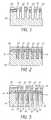
- FIG. 1is a schematic, cross-sectional side view of a substrate with trenches with a thin “pad oxide” grown over the surface of the substrate, a thicker layer of silicon nitride (Si 3 N 4 ), and a photoresist mask in accordance with a starting point for preferred embodiments of the present invention.
- FIG. 2is a schematic, cross-sectional side view of the substrate of FIG. 1 after spacers have been formed and the trench has been filled with a sacrificial material.
- FIG. 3is a schematic, cross-sectional side view of the substrate of FIG. 2 after one of the spacers has been removed and an etch into the substrate has been performed.
- FIG. 4is a schematic, cross-sectional side view of the substrate of FIG. 3 with the remaining spacer and sacrificial material removed.
- FIG. 5is a schematic, cross-sectional side view of the substrate of FIG. 4 after depositing insulating liners.
- FIG. 6is a schematic, cross-sectional side view of the substrate of FIG. 5 after etching the substrate using the liners as a mask.
- FIG. 7is a schematic, cross-sectional side view of the substrate of FIG. 6 after depositing an insulating material in the trench.
- FIG. 8is a schematic, cross-sectional side view of the substrate of FIG. 7 after depositing and recessing a digit line material in the trench.
- FIG. 9is a schematic, cross-sectional side view of the substrate of FIG. 8 after depositing an insulating material in the trench and etching back the insulating material.
- FIG. 10is a schematic, cross-sectional side view of the substrate of FIG. 9 after forming transistor pillars and cell capacitors.
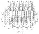
- FIG. 11is a schematic, cross-sectional side view of an array of memory cells formed in accordance with another embodiment of the invention.
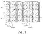
- FIG. 12is a schematic, cross-sectional plan view of the array of memory cells taken along lines 12 - 12 of FIGS. 10 or 11 .
- a buried digit lineis formed in a trench between rows of transistors. After forming trenches, spacers are formed within each trench. A sacrificial material is deposited within the trenches. One of the spacers is then removed from the trench, and the substrate below the removed spacer is etched to form an isolation window. After the isolation window is formed, the spacers and sacrificial material are removed. An insulating liner is formed conformally over the memory array. A spacer etch is then performed to preferentially etch horizontal surfaces. This exposes a portion of the trench. The exposed bottom of the trench is preferably etched at this stage to provide a recess in the substrate.
- the digit linecan be deposited directly into the recess. Otherwise, an insulating layer is preferably deposited into the trench before forming the digit line. An insulator is formed within the trench, and then etched back. Transistors and capacitors are completed at positions between and above the trenches to form the memory cell.
- a semiconductor substrate 10such as bulk silicon, like a silicon wafer, is provided.
- a cap layer 15may be formed over the substrate 10 in order to protect the substrate 10 from damage that could be caused during processing.
- the cap layeris preferably silicon nitride, but other insulating materials can also be used.
- the trenchesare then masked using photoresist 20 although other masking techniques can also be used.
- trenchesare formed in the substrate 10 .
- the trenchcan be formed in a variety of methods.
- an anisotropic dry etch processsuch as a reactive ion etch process, is used to etch the trenches.
- the trenchhas a depth of between about 1500 ⁇ and 6000 ⁇ , more preferably between about 2000 ⁇ and 3000 ⁇ .
- the width of the trenchesis preferably between about 100 ⁇ and 2000 ⁇ , more preferably between about 350 ⁇ (using a 0.04 ⁇ m process) and 1000 ⁇ (using a 0.100 ⁇ m process).
- An oxidation of the walls and base of the trench followed by an oxide etch stepmay also be performed in order to smooth trench walls. Skilled practitioners will appreciate that trenches can be formed in a variety of ways.
- a first set of spacers 22is formed on the walls of the trench.
- a conformal liner of spacer materialis deposited over the array.
- the spacer materialis preferably silicon dioxide, but can also be other materials which can be selectively etched relative to the surrounding materials.
- a spacer etchwhich preferentially removes horizontal layers relative to vertical layers, is then performed to expose a portion of the base of the trench and leaving the spacers 22 along the sidewalls of the trench.
- the spacers 22preferably have a thickness of between about 50 ⁇ and 600 ⁇ , more preferably between about 100 ⁇ and 300 ⁇ , representing about 1 ⁇ 3 of the trench width.
- a sacrificial material 25is deposited over the array, filling the trenches.
- the sacrificial material 25is polysilicon, but the sacrificial material can be any material that can be selectively etched to the material of the spacer 22 .
- one of the spacers 22 along the sidewalls of the trenchis removed.
- a photoresist mask 30is used during an etch of the sacrificial material 25 and one of the spacers 22 .
- the exposed sacrificial material 25is etched through the mask before the spacer 22 is removed. This etch process can be performed in distinct steps or in one etch step.
- the isolation window 35is asymmetric in that it will contact one side of the digit line, but not the other.
- the isolation windowextends between about 500 ⁇ and 3000 ⁇ below the trench floor, more preferably between about 1000 ⁇ and 2000 ⁇ .
- the mask and remaining sacrificial material and spacer materialare preferably removed after forming the isolation window 35 .
- a second set of spacersis formed.
- an insulating layer 40is conformally deposited over the array and the cap layer 15 .
- the insulating layer 40is preferably silicon nitride, but other electrically insulating materials can also be used.
- the insulating layerpreferably fills the isolation window 35 with a lower insulating layer.
- the insulating layer 40has a thickness along the sidewalls of between about 60 ⁇ and 600 ⁇ , more preferably between about 100 ⁇ and 200 ⁇ .
- Another spacer etchis performed to preferentially etch the horizontal surfaces of the insulating layer 40 and expose a second portion of the trench floor. This etch leaves remaining portions of the insulating layer 40 on the trench side walls in the form of insulating spacers that extend into the isolation window 35 .
- An etch processselectively etches the substrate material relative to the materials selected for the cap layer 15 and the insulating layer 40 to recess the exposed portion of the trench floor to form a lower recess 45 in the substrate 10 .
- this etch processetches between about 10 ⁇ and 3000 ⁇ of the substrate 10 , more preferably between about 200 ⁇ and 2500 521 .
- the insulating layer 40 along the sidewalls and the lower insulating layer in the isolation window 35insulate the surrounding substrate. As can be seen from FIG. 6 , one entire side of the lower recess 45 is exposed to the substrate 10 , while the other side of the lower recess 45 is partially bounded by the isolation window 35 .
- an insulating material 50is deposited into and recessed back in the lower recess 45 so that only one sidewall of the recess is electrically exposed to the digit line which will be formed within the lower recess 45 .
- the insulating material 50has a thickness of between about 100 ⁇ and 2000 ⁇ , more preferably between about 500 ⁇ and 800 ⁇ . In order to fully isolate the selected side of the lower recess, the thickness of the insulating material 50 is greater than the distance between the bottom of the lower recess and the bottom of the isolation window 33 . In other words, the insulating material 50 overlaps with the insulating lay 40 to completely isolate the right side of each trench.
- a conductive digit line 55is formed within the lower recess 45 .
- Preferred materials for the digit line 55include metals and metal alloys. Exemplary materials include titanium nitride, titanium, and tungsten.
- the digit line 55has a vertical thickness of between about 100 ⁇ and 2000 ⁇ , more preferably between about 300 ⁇ and 600 ⁇ .
- a multi-level digit line 55is formed with layers of several materials.
- a lower layer of titaniumis first deposited, serving as an adhesion layer, followed by a middle layer of titanium nitride, serving as a conductive barrier, and an upper layer of tungsten fills the remainder of the trench.
- the thickness of the middle barrier layeris preferably between about 20 ⁇ and 500 ⁇ , more preferably between about 40 ⁇ and 80 ⁇ .
- the thickness of the lower adhesion layeris preferably between about 10 ⁇ and 600 ⁇ , more preferably between about 100 ⁇ and 300 ⁇ .
- the thickness of the upper layeris preferably between about 100 ⁇ and 1500 ⁇ , more preferably between about 300 ⁇ and 600 ⁇ .
- Each such depositioncan line the lower recess 45 , thus extending over the trench sidewalls.
- the trenchis filled with an insulating material 60 .
- the insulating materialis an oxide, such as a tetraethyl orthosilicide (TEOS) oxide or a spin-on oxide.
- TEOStetraethyl orthosilicide
- CMPchemical mechanical polishing
- the insulating materialfills the trench, and is typically overflows by between about 50 ⁇ and 2000 ⁇ , more preferably between about 300 ⁇ and 600 ⁇ , before CMP or other etch back.
- the buried digit lines 55are then used to form a DRAM array.
- An exemplary arrayis seen after several stages of processing in FIG. 10 .
- Several DRAM processcan be used to form the memory array.
- One example processis found in U.S. patent application Ser. No. 10/934,621 of Tang, et. al, the disclosure of which is hereby incorporated herein by reference.
- a transistor pillar 65is formed on the substrate between the trenches.
- the pillarsare epitaxial silicon, though in other arrangements the pillars can be etched from a substrate.
- a gate oxide 70is then formed on the sides of the transistor pillars 65 .
- a source regionis formed along ridges between the trenches, preferably contacting the transistor pillar.
- the drainis formed at the top of the transistor pillar 65 and the body of the pillar defines the transistor channel.
- a word line 75is formed between neighboring cells.
- the word line 75is a conductive polysilicon and may include strapping self-aligned silicide.
- each word linesurrounds a row of transistors and serves as a gate electrode for each of the transistors in the row.
- An insulating layer 80is deposited over the word lines 75 .
- the top of the transistor pillar 65is then exposed to form electrical contact to an overlying stacked capacitor.
- the capacitor electrodeis a container capacitor.
- a bottom electrode 90is formed electrically connected to the transistor pillar 65 . It will be understood that as intermediate contact plug can be employed between the pillar 65 and the bottom electrode 90 .
- the bottom electrode 90comprises a conductive metal or metal alloy.
- a capacitor dielectric(not pictured) is then formed over the bottom electrode.
- a top electrodeis then formed the dielectric.
- the top electrodeis a common reference electrode for the whole array.
- VSGvertical surround gate
- the digit line 55is electrically connected to the substrate 10 , and particularly to the transistor sources, on one side of the trench, and isolated by the isolation liner 40 on the other side (right side in FIG. 10 ).
- the bottom of the insulating liner 40 in the isolation window 35extends below or even with the bottom of the digit line 55 .
- an insulator 50is formed beneath the digit line 55 within the lower recess 45 .
- the digit line 55is preferably isolated from above by an insulating material 60 .
- vertical transistorsare formed between the trenches.
- the vertical transistorsinclude transistor pillars 65 over the substrate 10 .
- a plurality of transistor pillars 65are formed on a ridge running parallel between the trenches in the dimension into and out of the paper.
- a gate oxide 71surrounds the sidewalls of the transistor pillar 65 .
- a word line 75serves as the gate electrode for each of a plurality of transistors in a row.
- An insulating layer 80is formed over the word line 75 .
- a bottom container capacitor electrode 90is formed over each transistor pillar.
- a capacitor dielectric and top electrodeis preferably formed over each of the electrodes.
- the isolation windowis extended below the bottom of the subsequently formed lower recess 45 a .
- the isolation window 35 ais filled with the insulating layer 40 a .
- the subsequent lower recess 45 aextends to approximately the same depth or less deep than the isolation window 35 a .
- the bottom of the isolation window 35 ais 100 ⁇ to 2000 ⁇ below the bottom of the digit line 55 a
- more preferably the bottom of the isolation window 35 ais 500 ⁇ to 800 ⁇ below the bottom of the digit line 55 a .
- the lower insulating material 50 of FIG. 7can thus be omitted, saving the deposition and recess steps therefore. Accordingly, the digit line 55 a is deposited directly into the lower recess 45 a.
- the bottom of the insulating material 40 a in the isolation window 35 apreferably extends below the digit line 55 a or is co-extensive with the bottom of the digit line 55 a .
- the top edge of the digit line 55 ais isolated from the transistor channel by the isolation liner 40 a.
- the resultant buried digit line 55 or 55 adirectly contacts the ridge of the substrate 10 along which a column of source regions 95 are formed.
- the bit digit line 55 or 55 ais in continuous contact with the ridge of substrate material 10 , such that no independent bit line contact structure is required. Rather, the digit line 55 or 55 a intermittently contacts source regions along its length. It will be understood that the source regions extend upwards to the surface of the substrate 10 , where epitaxial pillars extend upwards and form the channel regions of the transistors.
- Orthogonal to the digit lines 55 or 55 aare a plurality of word lines 75 , shown in dotted lines in FIG.
- the insulating layer 40 or 40 aelectrically separates the digit line 55 or 55 a from the next adjacent ridge of substrate material 10 .
- the digit line 55 or 55 adirectly contacts the substrate ridge 10 in the source regions, no separate contact structure is required. Not only does this save the additional process steps for forming a contact structure, but also save the additional space that would be otherwise required for making separate bit line contacts.
Landscapes
- Engineering & Computer Science (AREA)
- Manufacturing & Machinery (AREA)
- Semiconductor Memories (AREA)
Abstract
Description
- This application is a divisional of U.S. application Ser. No. 11/036,163, filed on Jan. 14, 2005, the entirety of which is hereby incorporated herein by reference.
- The present invention relates to the field of integrated circuit fabrication, specifically to the formation of memory arrays.
- Since the introduction of the digital computer, electronic storage devices have been a vital resource for the retention of data. Conventional semiconductor electronic storage devices, such as Dynamic Random Access Memory (DRAM), typically incorporate capacitor and transistor structures in which the capacitors temporarily store data based on the charged state of the capacitor structure. In general, this type of semiconductor Random Access Memory (RAM) often requires densely packed capacitor structures that are easily accessible for electrical interconnection.
- The capacitor and transistor structures are generally known as memory cells. The memory cells are arranged into memory arrays. The memory cells are addressed via a word line and a digit line, one of which addresses a “column” of memory cells while the other addresses a “row” of memory cells.
- In many DRAM devices, the digit line is buried below the upper level of the substrate. One example of this is burying the digit line within the isolation trench. However, this can often involve several complicated steps. Furthermore, as integrated circuit designs become more dense, it becomes more difficult to isolate a buried digit line within its trench and to make contact with individual transistors in the array.
- Thus, simpler and more reliable methods for forming, isolating, and contacting buried digit lines are desired.
- In accordance with one aspect of the invention, a method is provided for forming an integrated circuit. The method includes forming an elongated trench between a first transistor active region and a second transistor active region. An isolation element is deposited asymmetrically within the trench in contact with the second transistor active region. A bit line structure is deposited within the trench in direct contact with the active region and the isolation element, wherein the isolation element is positioned between the bit line structure and the second transistor active region.
- In accordance with another aspect of the invention, a method is provided for forming a buried digit line. The method includes forming a trench in a substrate with a base and side walls. A first spacer is formed along a first trench side wall and a second spacer along a second trench side wall. The trench is filled with a first sacrificial material after forming the first spacer and the second spacer. The second spacer is removed to expose a portion of a base of the trench after filling the trench with the first sacrificial material. The exposed first portion of the base of the trench is etched to form an isolation window having a first depth. A first insulating liner is deposited along the first trench wall and the second insulating liner is deposited along the second trench side wall into the isolation window. A recess is formed in the substrate by etching a second exposed portion of the base of the trench between the first liner and the second liner to a second depth. A digit line is then formed in the recess.
- In accordance with another aspect of the invention, a method of forming a memory array is provided. The method includes forming an elongated trench having first and second sides in a substrate. An asymmetric isolation window is formed in the trench using sacrificial spacers, where the asymmetric isolation window is formed along the second side of the trench. Insulating spacers are deposited along the sides of the trench and fill the insulation window. A digit line recess is formed between the insulating spacers in the substrate beneath the trench. A digit line is formed in the digit line recess. The digit line electrically connects to a first memory cell on the first side and is electrically isolated by the asymmetric isolation window from a second memory cell on the second side.
- In accordance with another aspect of the invention, a computer memory structure is provided. The structure includes a plurality of active regions in a substrate, where the active regions are arranged in a plurality of columns. A trench in the substrate separates a first column from a second column. A digit line in the trench directly contacts the first column. A filled asymmetric isolation window within the trench separates the digit line from the second column.
- In accordance with another aspect of the invention, an integrated circuit is provided, including a first elongated semiconductor ridge and a second elongated semiconductor ridge parallel to and spaced from the first ridge. The first and second ridges separated by a trench. Each of the first and second ridges serve as active areas for a plurality of transistors along the lengths of the ridges. The trench includes a conductive line in continuous electrical contact with the first ridge. An insulating element within the trench separates the conductive line from the second ridge.
- These and other aspects of the invention will be better understood from the detailed description below and the appended drawings, which are meant to illustrate and not to limit the invention, and in which:
FIG. 1 is a schematic, cross-sectional side view of a substrate with trenches with a thin “pad oxide” grown over the surface of the substrate, a thicker layer of silicon nitride (Si3N4), and a photoresist mask in accordance with a starting point for preferred embodiments of the present invention.FIG. 2 is a schematic, cross-sectional side view of the substrate ofFIG. 1 after spacers have been formed and the trench has been filled with a sacrificial material.FIG. 3 is a schematic, cross-sectional side view of the substrate ofFIG. 2 after one of the spacers has been removed and an etch into the substrate has been performed.FIG. 4 is a schematic, cross-sectional side view of the substrate ofFIG. 3 with the remaining spacer and sacrificial material removed.FIG. 5 is a schematic, cross-sectional side view of the substrate ofFIG. 4 after depositing insulating liners.FIG. 6 is a schematic, cross-sectional side view of the substrate ofFIG. 5 after etching the substrate using the liners as a mask.FIG. 7 is a schematic, cross-sectional side view of the substrate ofFIG. 6 after depositing an insulating material in the trench.FIG. 8 is a schematic, cross-sectional side view of the substrate ofFIG. 7 after depositing and recessing a digit line material in the trench.FIG. 9 is a schematic, cross-sectional side view of the substrate ofFIG. 8 after depositing an insulating material in the trench and etching back the insulating material.FIG. 10 is a schematic, cross-sectional side view of the substrate ofFIG. 9 after forming transistor pillars and cell capacitors.FIG. 11 is a schematic, cross-sectional side view of an array of memory cells formed in accordance with another embodiment of the invention.FIG. 12 is a schematic, cross-sectional plan view of the array of memory cells taken along lines12-12 of FIGS.10 or11.- In a preferred embodiment, a buried digit line is formed in a trench between rows of transistors. After forming trenches, spacers are formed within each trench. A sacrificial material is deposited within the trenches. One of the spacers is then removed from the trench, and the substrate below the removed spacer is etched to form an isolation window. After the isolation window is formed, the spacers and sacrificial material are removed. An insulating liner is formed conformally over the memory array. A spacer etch is then performed to preferentially etch horizontal surfaces. This exposes a portion of the trench. The exposed bottom of the trench is preferably etched at this stage to provide a recess in the substrate. If the insulating liner reaches the bottom of this recess, then the digit line can be deposited directly into the recess. Otherwise, an insulating layer is preferably deposited into the trench before forming the digit line. An insulator is formed within the trench, and then etched back. Transistors and capacitors are completed at positions between and above the trenches to form the memory cell.
- Referring now to an embodiment illustrated in
FIG. 1 , asemiconductor substrate 10, such as bulk silicon, like a silicon wafer, is provided. Acap layer 15 may be formed over thesubstrate 10 in order to protect thesubstrate 10 from damage that could be caused during processing. The cap layer is preferably silicon nitride, but other insulating materials can also be used. Preferably, the trenches are then masked usingphotoresist 20 although other masking techniques can also be used. - In a first step, trenches are formed in the
substrate 10. The trench can be formed in a variety of methods. Preferably, an anisotropic dry etch process, such as a reactive ion etch process, is used to etch the trenches. In a preferred embodiment the trench has a depth of between about 1500 Å and 6000 Å, more preferably between about 2000 Å and 3000 Å. The width of the trenches is preferably between about 100 Å and 2000 Å, more preferably between about 350 Å (using a 0.04 μm process) and 1000 Å (using a 0.100 μm process). An oxidation of the walls and base of the trench followed by an oxide etch step may also be performed in order to smooth trench walls. Skilled practitioners will appreciate that trenches can be formed in a variety of ways. - As seen in
FIG. 2 , after the trench is formed, a first set ofspacers 22 is formed on the walls of the trench. Preferably, a conformal liner of spacer material is deposited over the array. The spacer material is preferably silicon dioxide, but can also be other materials which can be selectively etched relative to the surrounding materials. A spacer etch, which preferentially removes horizontal layers relative to vertical layers, is then performed to expose a portion of the base of the trench and leaving thespacers 22 along the sidewalls of the trench. Thespacers 22 preferably have a thickness of between about 50 Å and 600 Å, more preferably between about 100 Å and 300 Å, representing about ⅓ of the trench width. - After forming the
spacers 22, asacrificial material 25 is deposited over the array, filling the trenches. In a preferred embodiment, thesacrificial material 25 is polysilicon, but the sacrificial material can be any material that can be selectively etched to the material of thespacer 22. - Referring now to
FIG. 3 , one of thespacers 22 along the sidewalls of the trench is removed. In a preferred embodiment, aphotoresist mask 30 is used during an etch of thesacrificial material 25 and one of thespacers 22. However, skilled practitioners will appreciate other masking techniques can be used. The exposedsacrificial material 25 is etched through the mask before thespacer 22 is removed. This etch process can be performed in distinct steps or in one etch step. - After one
spacer 22 is removed, a portion of the trench floor is left exposed. An etch process which will etch thesubstrate 10 selectively to thesacrificial material 25 is then performed to form an isolation window orslot 35. Preferably, theisolation window 35 is asymmetric in that it will contact one side of the digit line, but not the other. In a preferred embodiment, the isolation window extends between about 500 Å and 3000 Å below the trench floor, more preferably between about 1000 Å and 2000 Å. - As seen in
FIG. 4 , the mask and remaining sacrificial material and spacer material are preferably removed after forming theisolation window 35. - In
FIG. 5 , a second set of spacers is formed. First, an insulatinglayer 40 is conformally deposited over the array and thecap layer 15. The insulatinglayer 40 is preferably silicon nitride, but other electrically insulating materials can also be used. The insulating layer preferably fills theisolation window 35 with a lower insulating layer. Preferably the insulatinglayer 40 has a thickness along the sidewalls of between about 60 Å and 600 Å, more preferably between about 100 Å and 200 Å. - After the conformal insulating layer is deposited, another spacer etch is performed to preferentially etch the horizontal surfaces of the insulating
layer 40 and expose a second portion of the trench floor. This etch leaves remaining portions of the insulatinglayer 40 on the trench side walls in the form of insulating spacers that extend into theisolation window 35. - An etch process selectively etches the substrate material relative to the materials selected for the
cap layer 15 and the insulatinglayer 40 to recess the exposed portion of the trench floor to form alower recess 45 in thesubstrate 10. In a preferred embodiment, this etch process etches between about 10 Å and 3000 Å of thesubstrate 10, more preferably between about 200 Å and 2500521 . The insulatinglayer 40 along the sidewalls and the lower insulating layer in theisolation window 35 insulate the surrounding substrate. As can be seen fromFIG. 6 , one entire side of thelower recess 45 is exposed to thesubstrate 10, while the other side of thelower recess 45 is partially bounded by theisolation window 35. - In
FIG. 7 , an insulatingmaterial 50 is deposited into and recessed back in thelower recess 45 so that only one sidewall of the recess is electrically exposed to the digit line which will be formed within thelower recess 45. In a preferred embodiment, the insulatingmaterial 50 has a thickness of between about 100 Å and 2000 Å, more preferably between about 500 Å and 800 Å. In order to fully isolate the selected side of the lower recess, the thickness of the insulatingmaterial 50 is greater than the distance between the bottom of the lower recess and the bottom of the isolation window33. In other words, the insulatingmaterial 50 overlaps with the insulatinglay 40 to completely isolate the right side of each trench. - As illustrated in
FIG. 8 , once one side of thelower recess 45 is completely electrically isolated, aconductive digit line 55 is formed within thelower recess 45. Preferred materials for thedigit line 55 include metals and metal alloys. Exemplary materials include titanium nitride, titanium, and tungsten. Preferably, thedigit line 55 has a vertical thickness of between about 100 Å and 2000 Å, more preferably between about 300 Å and 600 Å. - In one embodiment, a
multi-level digit line 55 is formed with layers of several materials. In a preferred embodiment, a lower layer of titanium is first deposited, serving as an adhesion layer, followed by a middle layer of titanium nitride, serving as a conductive barrier, and an upper layer of tungsten fills the remainder of the trench. The thickness of the middle barrier layer is preferably between about 20 Å and 500 Å, more preferably between about 40 Å and 80 Å. The thickness of the lower adhesion layer is preferably between about 10 Å and 600 Å, more preferably between about 100 Å and 300 Å. The thickness of the upper layer is preferably between about 100 Å and 1500 Å, more preferably between about 300 Å and 600 Å. Each such deposition can line thelower recess 45, thus extending over the trench sidewalls. - As seen in
FIG. 9 , after depositing and recessing thedigit line 55, the trench is filled with an insulatingmaterial 60. In a preferred embodiment the insulating material is an oxide, such as a tetraethyl orthosilicide (TEOS) oxide or a spin-on oxide. The insulating material is then preferably etched back or planarized, through a process such as chemical mechanical polishing (CMP). In a preferred embodiment, the insulating material fills the trench, and is typically overflows by between about 50 Å and 2000 Å, more preferably between about 300 Å and 600 Å, before CMP or other etch back. - In a preferred embodiment, the buried
digit lines 55 are then used to form a DRAM array. An exemplary array is seen after several stages of processing inFIG. 10 . Several DRAM process can be used to form the memory array. One example process is found in U.S. patent application Ser. No. 10/934,621 of Tang, et. al, the disclosure of which is hereby incorporated herein by reference. - In the illustrated embodiment of
FIG. 10 , atransistor pillar 65 is formed on the substrate between the trenches. In a preferred embodiment, the pillars are epitaxial silicon, though in other arrangements the pillars can be etched from a substrate. Agate oxide 70 is then formed on the sides of thetransistor pillars 65. In a preferred embodiment, a source region is formed along ridges between the trenches, preferably contacting the transistor pillar. In preferred embodiments, the drain is formed at the top of thetransistor pillar 65 and the body of the pillar defines the transistor channel. Aword line 75 is formed between neighboring cells. In a preferred embodiment, theword line 75 is a conductive polysilicon and may include strapping self-aligned silicide. While not apparent from the illustrated cross-section, a plurality of word lines are formed in a crossing pattern with the bit lines. In a preferred arrangement, each word line surrounds a row of transistors and serves as a gate electrode for each of the transistors in the row. An insulatinglayer 80 is deposited over the word lines75. The top of thetransistor pillar 65 is then exposed to form electrical contact to an overlying stacked capacitor. In a preferred embodiment, the capacitor electrode is a container capacitor. Abottom electrode 90 is formed electrically connected to thetransistor pillar 65. It will be understood that as intermediate contact plug can be employed between thepillar 65 and thebottom electrode 90. In a preferred embodiment, thebottom electrode 90 comprises a conductive metal or metal alloy. A capacitor dielectric (not pictured) is then formed over the bottom electrode. A top electrode is then formed the dielectric. In a preferred embodiment the top electrode is a common reference electrode for the whole array. - An exemplary process flow for the illustrated vertical surround gate (VSG) transistor is disclosed in U.S. application Ser. No. 10/934,621, filed Sep. 2, 2004, the disclosure of which is incorporated by reference herein. The skilled artisan will readily appreciate, however, that the buried bit line processes and structures disclosed herein are useful for a number of different transistor and memory array designs.
- Thus, in a preferred embodiment illustrated in
FIG. 10 , thedigit line 55 is electrically connected to thesubstrate 10, and particularly to the transistor sources, on one side of the trench, and isolated by theisolation liner 40 on the other side (right side inFIG. 10 ). Preferably, the bottom of the insulatingliner 40 in theisolation window 35 extends below or even with the bottom of thedigit line 55. In the illustrated embodiment, aninsulator 50 is formed beneath thedigit line 55 within thelower recess 45. Thedigit line 55 is preferably isolated from above by an insulatingmaterial 60. - In a preferred embodiment, vertical transistors are formed between the trenches. The vertical transistors include
transistor pillars 65 over thesubstrate 10. Preferably, a plurality oftransistor pillars 65 are formed on a ridge running parallel between the trenches in the dimension into and out of the paper. A gate oxide71 surrounds the sidewalls of thetransistor pillar 65. Preferably, aword line 75 serves as the gate electrode for each of a plurality of transistors in a row. An insulatinglayer 80 is formed over theword line 75. A bottomcontainer capacitor electrode 90 is formed over each transistor pillar. A capacitor dielectric and top electrode is preferably formed over each of the electrodes. These structures are arranged in a memory array. The number of cells, trenches, and digit lines may vary based upon the desired capacity of the memory array. - With reference to
FIG. 11 , in another embodiment, theisolation window 35a formed using the spacers as is extended deeper into thesubstrate 10 than in the embodiment ofFIG. 4 . Preferably, the isolation window is extended below the bottom of the subsequently formedlower recess 45a. As described above, theisolation window 35ais filled with the insulatinglayer 40a. The subsequentlower recess 45aextends to approximately the same depth or less deep than theisolation window 35a. Preferably the bottom of theisolation window 35ais 100 Å to 2000 Å below the bottom of thedigit line 55a, more preferably the bottom of theisolation window 35ais 500 Å to 800 Å below the bottom of thedigit line 55a. The lower insulatingmaterial 50 ofFIG. 7 can thus be omitted, saving the deposition and recess steps therefore. Accordingly, thedigit line 55ais deposited directly into thelower recess 45a. - In the resulting structure, the bottom of the insulating
material 40ain theisolation window 35apreferably extends below thedigit line 55aor is co-extensive with the bottom of thedigit line 55a. On the other side of the trench, the top edge of thedigit line 55ais isolated from the transistor channel by theisolation liner 40a. - As best seen from the cross-sectional plan of
FIG. 12 , the resultant burieddigit line substrate 10 along which a column ofsource regions 95 are formed. Thebit digit line substrate material 10, such that no independent bit line contact structure is required. Rather, thedigit line substrate 10, where epitaxial pillars extend upwards and form the channel regions of the transistors. Orthogonal to thedigit lines word lines 75, shown in dotted lines inFIG. 12 , overlapping a row of transistors and surrounding the pillar channel regions to define vertical surround gate (VSG) transistors. On one side of thedigit line structures layer digit line substrate material 10. - Advantageously, because the
digit line substrate ridge 10 in the source regions, no separate contact structure is required. Not only does this save the additional process steps for forming a contact structure, but also save the additional space that would be otherwise required for making separate bit line contacts. - It will be appreciated by those skilled in the art that various omissions, additions and modifications may be made to the methods and structures described above without departing from the scope of the invention. All such modifications and changes are intended to fall within the scope of the invention, as defined by the appended claims.
Claims (20)
Priority Applications (3)
| Application Number | Priority Date | Filing Date | Title |
|---|---|---|---|
| US11/491,461US7368365B2 (en) | 2005-01-14 | 2006-07-21 | Memory array buried digit line |
| US11/933,051US7768073B2 (en) | 2005-01-14 | 2007-10-31 | Memory array buried digit line |
| US12/836,404US8102008B2 (en) | 2005-01-14 | 2010-07-14 | Integrated circuit with buried digit line |
Applications Claiming Priority (2)
| Application Number | Priority Date | Filing Date | Title |
|---|---|---|---|
| US11/036,163US7229895B2 (en) | 2005-01-14 | 2005-01-14 | Memory array buried digit line |
| US11/491,461US7368365B2 (en) | 2005-01-14 | 2006-07-21 | Memory array buried digit line |
Related Parent Applications (1)
| Application Number | Title | Priority Date | Filing Date |
|---|---|---|---|
| US11/036,163DivisionUS7229895B2 (en) | 2005-01-14 | 2005-01-14 | Memory array buried digit line |
Related Child Applications (1)
| Application Number | Title | Priority Date | Filing Date |
|---|---|---|---|
| US11/933,051DivisionUS7768073B2 (en) | 2005-01-14 | 2007-10-31 | Memory array buried digit line |
Publications (2)
| Publication Number | Publication Date |
|---|---|
| US20060258119A1true US20060258119A1 (en) | 2006-11-16 |
| US7368365B2 US7368365B2 (en) | 2008-05-06 |
Family
ID=36684479
Family Applications (5)
| Application Number | Title | Priority Date | Filing Date |
|---|---|---|---|
| US11/036,163Expired - LifetimeUS7229895B2 (en) | 2005-01-14 | 2005-01-14 | Memory array buried digit line |
| US11/490,619Expired - LifetimeUS7601608B2 (en) | 2005-01-14 | 2006-07-21 | Memory array buried digit line |
| US11/491,461Expired - LifetimeUS7368365B2 (en) | 2005-01-14 | 2006-07-21 | Memory array buried digit line |
| US11/933,051Expired - LifetimeUS7768073B2 (en) | 2005-01-14 | 2007-10-31 | Memory array buried digit line |
| US12/836,404Expired - LifetimeUS8102008B2 (en) | 2005-01-14 | 2010-07-14 | Integrated circuit with buried digit line |
Family Applications Before (2)
| Application Number | Title | Priority Date | Filing Date |
|---|---|---|---|
| US11/036,163Expired - LifetimeUS7229895B2 (en) | 2005-01-14 | 2005-01-14 | Memory array buried digit line |
| US11/490,619Expired - LifetimeUS7601608B2 (en) | 2005-01-14 | 2006-07-21 | Memory array buried digit line |
Family Applications After (2)
| Application Number | Title | Priority Date | Filing Date |
|---|---|---|---|
| US11/933,051Expired - LifetimeUS7768073B2 (en) | 2005-01-14 | 2007-10-31 | Memory array buried digit line |
| US12/836,404Expired - LifetimeUS8102008B2 (en) | 2005-01-14 | 2010-07-14 | Integrated circuit with buried digit line |
Country Status (1)
| Country | Link |
|---|---|
| US (5) | US7229895B2 (en) |
Cited By (5)
| Publication number | Priority date | Publication date | Assignee | Title |
|---|---|---|---|---|
| US20070231980A1 (en)* | 2006-04-04 | 2007-10-04 | Micron Technology, Inc. | Etched nanofin transistors |
| US20070231985A1 (en)* | 2006-04-04 | 2007-10-04 | Micron Technology, Inc. | Grown nanofin transistors |
| US20080315279A1 (en)* | 2006-04-04 | 2008-12-25 | Micron Technology, Inc. | Nanowire transistor with surrounding gate |
| US20090155966A1 (en)* | 2006-04-04 | 2009-06-18 | Micron Technology, Inc. | Dram with nanofin transistors |
| CN102315160A (en)* | 2010-07-06 | 2012-01-11 | 海力士半导体有限公司 | Semiconductor device with one-side contact and fabrication method thereof |
Families Citing this family (201)
| Publication number | Priority date | Publication date | Assignee | Title |
|---|---|---|---|---|
| US5865361A (en) | 1997-09-23 | 1999-02-02 | United States Surgical Corporation | Surgical stapling apparatus |
| US6180508B1 (en)* | 1999-09-02 | 2001-01-30 | Micron Technology, Inc. | Methods of fabricating buried digit lines and semiconductor devices including same |
| US7229895B2 (en)* | 2005-01-14 | 2007-06-12 | Micron Technology, Inc | Memory array buried digit line |
| US7776715B2 (en) | 2005-07-26 | 2010-08-17 | Micron Technology, Inc. | Reverse construction memory cell |
| US20070117311A1 (en)* | 2005-11-23 | 2007-05-24 | Advanced Technology Development Facility, Inc. | Three-dimensional single transistor semiconductor memory device and methods for making same |
| US7557002B2 (en)* | 2006-08-18 | 2009-07-07 | Micron Technology, Inc. | Methods of forming transistor devices |
| US8584921B2 (en) | 2006-10-06 | 2013-11-19 | Covidien Lp | Surgical instrument with articulating tool assembly |
| US7989322B2 (en)* | 2007-02-07 | 2011-08-02 | Micron Technology, Inc. | Methods of forming transistors |
| US8061576B2 (en) | 2007-08-31 | 2011-11-22 | Tyco Healthcare Group Lp | Surgical instrument |
| US7618874B1 (en)* | 2008-05-02 | 2009-11-17 | Micron Technology, Inc. | Methods of forming capacitors |
| US7696056B2 (en)* | 2008-05-02 | 2010-04-13 | Micron Technology, Inc. | Methods of forming capacitors |
| KR101432619B1 (en)* | 2008-07-07 | 2014-08-21 | 삼성전자주식회사 | Semiconductor device and manufacturing method thereof |
| US7781283B2 (en)* | 2008-08-15 | 2010-08-24 | International Business Machines Corporation | Split-gate DRAM with MuGFET, design structure, and method of manufacture |
| US7979836B2 (en)* | 2008-08-15 | 2011-07-12 | International Business Machines Corporation | Split-gate DRAM with MuGFET, design structure, and method of manufacture |
| US8628544B2 (en) | 2008-09-23 | 2014-01-14 | Covidien Lp | Knife bar for surgical instrument |
| US7988028B2 (en) | 2008-09-23 | 2011-08-02 | Tyco Healthcare Group Lp | Surgical instrument having an asymmetric dynamic clamping member |
| US8184472B2 (en) | 2009-03-13 | 2012-05-22 | International Business Machines Corporation | Split-gate DRAM with lateral control-gate MuGFET |
| US7999332B2 (en)* | 2009-05-14 | 2011-08-16 | International Business Machines Corporation | Asymmetric semiconductor devices and method of fabricating |
| US20110042722A1 (en)* | 2009-08-21 | 2011-02-24 | Nanya Technology Corp. | Integrated circuit structure and memory array |
| JP2011077185A (en)* | 2009-09-29 | 2011-04-14 | Elpida Memory Inc | Semiconductor device, method of manufacturing semiconductor device, and data processing system |
| KR101576957B1 (en)* | 2009-10-22 | 2015-12-14 | 삼성전자주식회사 | Vertical semiconductor device, memory device, and manufacturing method thereof |
| KR101577411B1 (en)* | 2009-12-16 | 2015-12-15 | 삼성전자주식회사 | Method for fabricating vertical channel transistor |
| US8501578B2 (en)* | 2010-01-22 | 2013-08-06 | Estivation Properties Llc | Semiconductor structure formed without requiring thermal oxidation |
| US8497541B2 (en) | 2010-03-10 | 2013-07-30 | Micron Technology, Inc. | Memory having buried digit lines and methods of making the same |
| US8254173B2 (en) | 2010-08-31 | 2012-08-28 | Micron Technology, Inc. | NAND memory constructions |
| KR101699443B1 (en) | 2010-10-15 | 2017-01-25 | 삼성전자 주식회사 | Method for manufacturing semiconductor device having vertical channel transistor |
| US8361856B2 (en) | 2010-11-01 | 2013-01-29 | Micron Technology, Inc. | Memory cells, arrays of memory cells, and methods of forming memory cells |
| US8329567B2 (en) | 2010-11-03 | 2012-12-11 | Micron Technology, Inc. | Methods of forming doped regions in semiconductor substrates |
| KR101172272B1 (en)* | 2010-12-30 | 2012-08-09 | 에스케이하이닉스 주식회사 | Method for manufacturing semiconductor device with buried bitline |
| US8450175B2 (en) | 2011-02-22 | 2013-05-28 | Micron Technology, Inc. | Methods of forming a vertical transistor and at least a conductive line electrically coupled therewith |
| US8569831B2 (en) | 2011-05-27 | 2013-10-29 | Micron Technology, Inc. | Integrated circuit arrays and semiconductor constructions |
| US8740036B2 (en) | 2011-12-01 | 2014-06-03 | Covidien Lp | Surgical instrument with actuator spring arm |
| JP2013168569A (en)* | 2012-02-16 | 2013-08-29 | Elpida Memory Inc | Semiconductor device and manufacturing method of the same |
| US9036391B2 (en)* | 2012-03-06 | 2015-05-19 | Micron Technology, Inc. | Arrays of vertically-oriented transistors, memory arrays including vertically-oriented transistors, and memory cells |
| KR20130106159A (en)* | 2012-03-19 | 2013-09-27 | 에스케이하이닉스 주식회사 | Semiconductor device having buried bitline and fabricating the same |
| US9129896B2 (en) | 2012-08-21 | 2015-09-08 | Micron Technology, Inc. | Arrays comprising vertically-oriented transistors, integrated circuitry comprising a conductive line buried in silicon-comprising semiconductor material, methods of forming a plurality of conductive lines buried in silicon-comprising semiconductor material, and methods of forming an array comprising vertically-oriented transistors |
| US9006060B2 (en) | 2012-08-21 | 2015-04-14 | Micron Technology, Inc. | N-type field effect transistors, arrays comprising N-type vertically-oriented transistors, methods of forming an N-type field effect transistor, and methods of forming an array comprising vertically-oriented N-type transistors |
| US9478550B2 (en) | 2012-08-27 | 2016-10-25 | Micron Technology, Inc. | Arrays of vertically-oriented transistors, and memory arrays including vertically-oriented transistors |
| US9064745B2 (en) | 2012-08-29 | 2015-06-23 | International Business Machines Corporation | Sublithographic width finFET employing solid phase epitaxy |
| US9814463B2 (en) | 2013-03-13 | 2017-11-14 | Covidien Lp | Surgical stapling apparatus |
| US9668729B2 (en) | 2013-03-13 | 2017-06-06 | Covidien Lp | Surgical stapling apparatus |
| US12161322B2 (en) | 2013-03-13 | 2024-12-10 | Covidien Lp | Surgical stapling apparatus |
| US9629628B2 (en) | 2013-03-13 | 2017-04-25 | Covidien Lp | Surgical stapling apparatus |
| US9717498B2 (en) | 2013-03-13 | 2017-08-01 | Covidien Lp | Surgical stapling apparatus |
| US9111853B2 (en) | 2013-03-15 | 2015-08-18 | Micron Technology, Inc. | Methods of forming doped elements of semiconductor device structures |
| CN104109149B (en)* | 2013-04-22 | 2018-09-28 | 苏州泽璟生物制药有限公司 | Deuterated diaminopyrimidine compounds and the pharmaceutical composition comprising the compound |
| US9662108B2 (en) | 2013-08-30 | 2017-05-30 | Covidien Lp | Surgical stapling apparatus |
| JP6366708B2 (en) | 2013-11-04 | 2018-08-01 | コヴィディエン リミテッド パートナーシップ | Surgical fastener application device |
| CN105682567B (en) | 2013-11-04 | 2021-09-10 | 柯惠Lp公司 | Surgical fastener applying apparatus |
| CN105682568B (en) | 2013-11-04 | 2018-10-23 | 柯惠Lp公司 | Surgical fasteners bringing device |
| US9867613B2 (en) | 2013-12-19 | 2018-01-16 | Covidien Lp | Surgical staples and end effectors for deploying the same |
| US9848874B2 (en) | 2014-02-14 | 2017-12-26 | Covidien Lp | Small diameter endoscopic stapler |
| US9757126B2 (en) | 2014-03-31 | 2017-09-12 | Covidien Lp | Surgical stapling apparatus with firing lockout mechanism |
| US9668733B2 (en) | 2014-04-21 | 2017-06-06 | Covidien Lp | Stapling device with features to prevent inadvertent firing of staples |
| US9861366B2 (en) | 2014-05-06 | 2018-01-09 | Covidien Lp | Ejecting assembly for a surgical stapler |
| EP3142569B1 (en) | 2014-05-15 | 2023-12-27 | Covidien LP | Surgical fastener applying apparatus |
| US10039545B2 (en) | 2015-02-23 | 2018-08-07 | Covidien Lp | Double fire stapling |
| US10285698B2 (en) | 2015-02-26 | 2019-05-14 | Covidien Lp | Surgical apparatus |
| US10085749B2 (en) | 2015-02-26 | 2018-10-02 | Covidien Lp | Surgical apparatus with conductor strain relief |
| US9918717B2 (en) | 2015-03-18 | 2018-03-20 | Covidien Lp | Pivot mechanism for surgical device |
| US10463368B2 (en) | 2015-04-10 | 2019-11-05 | Covidien Lp | Endoscopic stapler |
| US10117650B2 (en) | 2015-05-05 | 2018-11-06 | Covidien Lp | Adapter assembly and loading units for surgical stapling devices |
| US10299789B2 (en) | 2015-05-05 | 2019-05-28 | Covidie LP | Adapter assembly for surgical stapling devices |
| US10039532B2 (en) | 2015-05-06 | 2018-08-07 | Covidien Lp | Surgical instrument with articulation assembly |
| CN107635481B (en) | 2015-05-25 | 2021-01-05 | 柯惠有限合伙公司 | Minor diameter surgical suturing device |
| US10349941B2 (en) | 2015-05-27 | 2019-07-16 | Covidien Lp | Multi-fire lead screw stapling device |
| US10172615B2 (en) | 2015-05-27 | 2019-01-08 | Covidien Lp | Multi-fire push rod stapling device |
| US10548599B2 (en) | 2015-07-20 | 2020-02-04 | Covidien Lp | Endoscopic stapler and staple |
| US9987012B2 (en) | 2015-07-21 | 2018-06-05 | Covidien Lp | Small diameter cartridge design for a surgical stapling instrument |
| US10064622B2 (en) | 2015-07-29 | 2018-09-04 | Covidien Lp | Surgical stapling loading unit with stroke counter and lockout |
| US10045782B2 (en) | 2015-07-30 | 2018-08-14 | Covidien Lp | Surgical stapling loading unit with stroke counter and lockout |
| US10213204B2 (en) | 2015-10-02 | 2019-02-26 | Covidien Lp | Micro surgical instrument and loading unit for use therewith |
| US10772632B2 (en) | 2015-10-28 | 2020-09-15 | Covidien Lp | Surgical stapling device with triple leg staples |
| US10595864B2 (en) | 2015-11-24 | 2020-03-24 | Covidien Lp | Adapter assembly for interconnecting electromechanical surgical devices and surgical loading units, and surgical systems thereof |
| US10111660B2 (en) | 2015-12-03 | 2018-10-30 | Covidien Lp | Surgical stapler flexible distal tip |
| US10966717B2 (en) | 2016-01-07 | 2021-04-06 | Covidien Lp | Surgical fastener apparatus |
| US10660623B2 (en) | 2016-01-15 | 2020-05-26 | Covidien Lp | Centering mechanism for articulation joint |
| DE102016101545B4 (en)* | 2016-01-28 | 2020-10-08 | Infineon Technologies Dresden Gmbh | METHOD OF MANUFACTURING A SEMICONDUCTOR DEVICE WITH SILICIDE LAYERS AND A SEMICONDUCTOR DEVICE |
| US10349937B2 (en) | 2016-02-10 | 2019-07-16 | Covidien Lp | Surgical stapler with articulation locking mechanism |
| US10420559B2 (en) | 2016-02-11 | 2019-09-24 | Covidien Lp | Surgical stapler with small diameter endoscopic portion |
| US10561419B2 (en) | 2016-05-04 | 2020-02-18 | Covidien Lp | Powered end effector assembly with pivotable channel |
| US11065022B2 (en) | 2016-05-17 | 2021-07-20 | Covidien Lp | Cutting member for a surgical instrument |
| US11642126B2 (en) | 2016-11-04 | 2023-05-09 | Covidien Lp | Surgical stapling apparatus with tissue pockets |
| US10631857B2 (en) | 2016-11-04 | 2020-04-28 | Covidien Lp | Loading unit for surgical instruments with low profile pushers |
| US10492784B2 (en) | 2016-11-08 | 2019-12-03 | Covidien Lp | Surgical tool assembly with compact firing assembly |
| US10463371B2 (en) | 2016-11-29 | 2019-11-05 | Covidien Lp | Reload assembly with spent reload indicator |
| US10709901B2 (en) | 2017-01-05 | 2020-07-14 | Covidien Lp | Implantable fasteners, applicators, and methods for brachytherapy |
| US10952767B2 (en) | 2017-02-06 | 2021-03-23 | Covidien Lp | Connector clip for securing an introducer to a surgical fastener applying apparatus |
| US20180235618A1 (en) | 2017-02-22 | 2018-08-23 | Covidien Lp | Loading unit for surgical instruments with low profile pushers |
| US11350915B2 (en) | 2017-02-23 | 2022-06-07 | Covidien Lp | Surgical stapler with small diameter endoscopic portion |
| US10849621B2 (en) | 2017-02-23 | 2020-12-01 | Covidien Lp | Surgical stapler with small diameter endoscopic portion |
| US10299790B2 (en) | 2017-03-03 | 2019-05-28 | Covidien Lp | Adapter with centering mechanism for articulation joint |
| US10660641B2 (en) | 2017-03-16 | 2020-05-26 | Covidien Lp | Adapter with centering mechanism for articulation joint |
| US11324502B2 (en) | 2017-05-02 | 2022-05-10 | Covidien Lp | Surgical loading unit including an articulating end effector |
| US10603035B2 (en) | 2017-05-02 | 2020-03-31 | Covidien Lp | Surgical loading unit including an articulating end effector |
| US10524784B2 (en) | 2017-05-05 | 2020-01-07 | Covidien Lp | Surgical staples with expandable backspan |
| US10390826B2 (en) | 2017-05-08 | 2019-08-27 | Covidien Lp | Surgical stapling device with elongated tool assembly and methods of use |
| US10420551B2 (en) | 2017-05-30 | 2019-09-24 | Covidien Lp | Authentication and information system for reusable surgical instruments |
| US10478185B2 (en) | 2017-06-02 | 2019-11-19 | Covidien Lp | Tool assembly with minimal dead space |
| US10586765B2 (en) | 2017-06-22 | 2020-03-10 | Tokyo Electron Limited | Buried power rails |
| US10624636B2 (en) | 2017-08-23 | 2020-04-21 | Covidien Lp | Surgical stapling device with floating staple cartridge |
| US10806452B2 (en) | 2017-08-24 | 2020-10-20 | Covidien Lp | Loading unit for a surgical stapling instrument |
| US10925603B2 (en) | 2017-11-14 | 2021-02-23 | Covidien Lp | Reload with articulation stabilization system |
| US10863987B2 (en) | 2017-11-16 | 2020-12-15 | Covidien Lp | Surgical instrument with imaging device |
| US10945732B2 (en) | 2018-01-17 | 2021-03-16 | Covidien Lp | Surgical stapler with self-returning assembly |
| CA3090020A1 (en) | 2018-03-02 | 2019-09-06 | Covidien Lp | Surgical stapling instrument |
| US10849622B2 (en) | 2018-06-21 | 2020-12-01 | Covidien Lp | Articulated stapling with fire lock |
| US10736631B2 (en) | 2018-08-07 | 2020-08-11 | Covidien Lp | End effector with staple cartridge ejector |
| US10849620B2 (en) | 2018-09-14 | 2020-12-01 | Covidien Lp | Connector mechanisms for surgical stapling instruments |
| US11510669B2 (en) | 2020-09-29 | 2022-11-29 | Covidien Lp | Hand-held surgical instruments |
| US11090051B2 (en) | 2018-10-23 | 2021-08-17 | Covidien Lp | Surgical stapling device with floating staple cartridge |
| US11197673B2 (en) | 2018-10-30 | 2021-12-14 | Covidien Lp | Surgical stapling instruments and end effector assemblies thereof |
| US10930734B2 (en) | 2018-10-30 | 2021-02-23 | International Business Machines Corporation | Nanosheet FET bottom isolation |
| US10912563B2 (en) | 2019-01-02 | 2021-02-09 | Covidien Lp | Stapling device including tool assembly stabilizing member |
| US11344297B2 (en) | 2019-02-28 | 2022-05-31 | Covidien Lp | Surgical stapling device with independently movable jaws |
| US11259808B2 (en) | 2019-03-13 | 2022-03-01 | Covidien Lp | Tool assemblies with a gap locking member |
| US11284893B2 (en) | 2019-04-02 | 2022-03-29 | Covidien Lp | Stapling device with articulating tool assembly |
| US11284892B2 (en) | 2019-04-02 | 2022-03-29 | Covidien Lp | Loading unit and adapter with modified coupling assembly |
| US11241228B2 (en) | 2019-04-05 | 2022-02-08 | Covidien Lp | Surgical instrument including an adapter assembly and an articulating surgical loading unit |
| US11224424B2 (en) | 2019-08-02 | 2022-01-18 | Covidien Lp | Linear stapling device with vertically movable knife |
| US11406385B2 (en) | 2019-10-11 | 2022-08-09 | Covidien Lp | Stapling device with a gap locking member |
| US11123068B2 (en) | 2019-11-08 | 2021-09-21 | Covidien Lp | Surgical staple cartridge |
| US11974743B2 (en) | 2019-12-02 | 2024-05-07 | Covidien Lp | Linear stapling device with a gap locking member |
| US11707274B2 (en) | 2019-12-06 | 2023-07-25 | Covidien Lp | Articulating mechanism for surgical instrument |
| US11109862B2 (en) | 2019-12-12 | 2021-09-07 | Covidien Lp | Surgical stapling device with flexible shaft |
| US12383260B2 (en) | 2019-12-13 | 2025-08-12 | Covidien Lp | Surgical stapler with universal tip reload |
| US11737747B2 (en) | 2019-12-17 | 2023-08-29 | Covidien Lp | Hand-held surgical instruments |
| US11278282B2 (en) | 2020-01-31 | 2022-03-22 | Covidien Lp | Stapling device with selective cutting |
| US11452524B2 (en) | 2020-01-31 | 2022-09-27 | Covidien Lp | Surgical stapling device with lockout |
| US12156651B2 (en) | 2020-02-03 | 2024-12-03 | Covidien Lp | Surgical stapling device |
| JP2023523507A (en) | 2020-02-14 | 2023-06-06 | コヴィディエン リミテッド パートナーシップ | A cartridge holder for surgical staples and having ridges on the peripheral wall for gripping tissue |
| CN115103642A (en) | 2020-02-14 | 2022-09-23 | 柯惠有限合伙公司 | surgical stapler |
| US11344301B2 (en) | 2020-03-02 | 2022-05-31 | Covidien Lp | Surgical stapling device with replaceable reload assembly |
| US11344302B2 (en) | 2020-03-05 | 2022-05-31 | Covidien Lp | Articulation mechanism for surgical stapling device |
| US11707278B2 (en) | 2020-03-06 | 2023-07-25 | Covidien Lp | Surgical stapler tool assembly to minimize bleeding |
| US11246593B2 (en) | 2020-03-06 | 2022-02-15 | Covidien Lp | Staple cartridge |
| US11357505B2 (en) | 2020-03-10 | 2022-06-14 | Covidien Lp | Surgical stapling apparatus with firing lockout mechanism |
| US11317911B2 (en) | 2020-03-10 | 2022-05-03 | Covidien Lp | Tool assembly with replaceable cartridge assembly |
| US11406383B2 (en) | 2020-03-17 | 2022-08-09 | Covidien Lp | Fire assisted powered EGIA handle |
| US12108953B2 (en) | 2020-03-24 | 2024-10-08 | Covidien Lp | Surgical stapling device with replaceable staple cartridge |
| US11426159B2 (en) | 2020-04-01 | 2022-08-30 | Covidien Lp | Sled detection device |
| US11331098B2 (en) | 2020-04-01 | 2022-05-17 | Covidien Lp | Sled detection device |
| US11504117B2 (en) | 2020-04-02 | 2022-11-22 | Covidien Lp | Hand-held surgical instruments |
| US11937794B2 (en) | 2020-05-11 | 2024-03-26 | Covidien Lp | Powered handle assembly for surgical devices |
| US11191537B1 (en) | 2020-05-12 | 2021-12-07 | Covidien Lp | Stapling device with continuously parallel jaws |
| US11406387B2 (en) | 2020-05-12 | 2022-08-09 | Covidien Lp | Surgical stapling device with replaceable staple cartridge |
| US11534167B2 (en) | 2020-05-28 | 2022-12-27 | Covidien Lp | Electrotaxis-conducive stapling |
| US11191538B1 (en) | 2020-06-08 | 2021-12-07 | Covidien Lp | Surgical stapling device with parallel jaw closure |
| US11844517B2 (en) | 2020-06-25 | 2023-12-19 | Covidien Lp | Linear stapling device with continuously parallel jaws |
| US11324500B2 (en) | 2020-06-30 | 2022-05-10 | Covidien Lp | Surgical stapling device |
| US12023027B2 (en) | 2020-07-02 | 2024-07-02 | Covidien Lp | Surgical stapling device with compressible staple cartridge |
| US11446028B2 (en) | 2020-07-09 | 2022-09-20 | Covidien Lp | Tool assembly with pivotable clamping beam |
| US12349902B2 (en) | 2020-07-09 | 2025-07-08 | Covidien Lp | Powered handle assembly for surgical devices |
| US11517305B2 (en) | 2020-07-09 | 2022-12-06 | Covidien Lp | Contoured staple pusher |
| EP4185215A4 (en) | 2020-07-21 | 2024-04-03 | Covidien LP | Shipping cover for staple cartridge |
| US11266402B2 (en) | 2020-07-30 | 2022-03-08 | Covidien Lp | Sensing curved tip for surgical stapling instruments |
| US11439392B2 (en) | 2020-08-03 | 2022-09-13 | Covidien Lp | Surgical stapling device and fastener for pathological exam |
| US11395654B2 (en) | 2020-08-07 | 2022-07-26 | Covidien Lp | Surgical stapling device with articulation braking assembly |
| US11602342B2 (en) | 2020-08-27 | 2023-03-14 | Covidien Lp | Surgical stapling device with laser probe |
| US11678878B2 (en) | 2020-09-16 | 2023-06-20 | Covidien Lp | Articulation mechanism for surgical stapling device |
| US11660092B2 (en) | 2020-09-29 | 2023-05-30 | Covidien Lp | Adapter for securing loading units to handle assemblies of surgical stapling instruments |
| US11406384B2 (en) | 2020-10-05 | 2022-08-09 | Covidien Lp | Stapling device with drive assembly stop member |
| US11576674B2 (en) | 2020-10-06 | 2023-02-14 | Covidien Lp | Surgical stapling device with articulation lock assembly |
| US11890007B2 (en) | 2020-11-18 | 2024-02-06 | Covidien Lp | Stapling device with flex cable and tensioning mechanism |
| US11737774B2 (en) | 2020-12-04 | 2023-08-29 | Covidien Lp | Surgical instrument with articulation assembly |
| US11819200B2 (en) | 2020-12-15 | 2023-11-21 | Covidien Lp | Surgical instrument with articulation assembly |
| US11553914B2 (en) | 2020-12-22 | 2023-01-17 | Covidien Lp | Surgical stapling device with parallel jaw closure |
| WO2022140080A1 (en) | 2020-12-23 | 2022-06-30 | Covidien Lp | Surgical instrument including a decoupling mechanism |
| US11744582B2 (en) | 2021-01-05 | 2023-09-05 | Covidien Lp | Surgical stapling device with firing lockout mechanism |
| US11759206B2 (en) | 2021-01-05 | 2023-09-19 | Covidien Lp | Surgical stapling device with firing lockout mechanism |
| US11517313B2 (en) | 2021-01-27 | 2022-12-06 | Covidien Lp | Surgical stapling device with laminated drive member |
| US11759207B2 (en) | 2021-01-27 | 2023-09-19 | Covidien Lp | Surgical stapling apparatus with adjustable height clamping member |
| US11717300B2 (en) | 2021-03-11 | 2023-08-08 | Covidien Lp | Surgical stapling apparatus with integrated visualization |
| US11974750B2 (en) | 2021-03-26 | 2024-05-07 | Covidien Lp | Surgical staple cartridge |
| US11497495B2 (en) | 2021-03-31 | 2022-11-15 | Covidien Lp | Continuous stapler strip for use with a surgical stapling device |
| US11666330B2 (en) | 2021-04-05 | 2023-06-06 | Covidien Lp | Surgical stapling device with lockout mechanism |
| US11576670B2 (en) | 2021-05-06 | 2023-02-14 | Covidien Lp | Surgical stapling device with optimized drive assembly |
| US11812956B2 (en) | 2021-05-18 | 2023-11-14 | Covidien Lp | Dual firing radial stapling device |
| US11696755B2 (en) | 2021-05-19 | 2023-07-11 | Covidien Lp | Surgical stapling device with reload assembly removal lockout |
| CN117337154A (en) | 2021-05-21 | 2024-01-02 | 柯惠有限合伙公司 | Articulated assemblies for surgical devices |
| US11771423B2 (en) | 2021-05-25 | 2023-10-03 | Covidien Lp | Powered stapling device with manual retraction |
| US11510673B1 (en) | 2021-05-25 | 2022-11-29 | Covidien Lp | Powered stapling device with manual retraction |
| US11701119B2 (en) | 2021-05-26 | 2023-07-18 | Covidien Lp | Powered stapling device with rack release |
| US11576675B2 (en) | 2021-06-07 | 2023-02-14 | Covidien Lp | Staple cartridge with knife |
| US11707275B2 (en) | 2021-06-29 | 2023-07-25 | Covidien Lp | Asymmetrical surgical stapling device |
| US11617579B2 (en) | 2021-06-29 | 2023-04-04 | Covidien Lp | Ultra low profile surgical stapling instrument for tissue resections |
| US11602344B2 (en) | 2021-06-30 | 2023-03-14 | Covidien Lp | Surgical stapling apparatus with firing lockout assembly |
| US11540831B1 (en) | 2021-08-12 | 2023-01-03 | Covidien Lp | Staple cartridge with actuation sled detection |
| US11779334B2 (en) | 2021-08-19 | 2023-10-10 | Covidien Lp | Surgical stapling device including a manual retraction assembly |
| US12023028B2 (en) | 2021-08-20 | 2024-07-02 | Covidien Lp | Articulating surgical stapling apparatus with pivotable knife bar guide assembly |
| US11707277B2 (en) | 2021-08-20 | 2023-07-25 | Covidien Lp | Articulating surgical stapling apparatus with pivotable knife bar guide assembly |
| US11576671B1 (en) | 2021-08-20 | 2023-02-14 | Covidien Lp | Small diameter linear surgical stapling apparatus |
| US11864761B2 (en) | 2021-09-14 | 2024-01-09 | Covidien Lp | Surgical instrument with illumination mechanism |
| US11660094B2 (en) | 2021-09-29 | 2023-05-30 | Covidien Lp | Surgical fastening instrument with two-part surgical fasteners |
| US11653922B2 (en) | 2021-09-29 | 2023-05-23 | Covidien Lp | Surgical stapling device with firing lockout mechanism |
| US11849949B2 (en) | 2021-09-30 | 2023-12-26 | Covidien Lp | Surgical stapling device with firing lockout member |
| US12035909B2 (en) | 2021-10-13 | 2024-07-16 | Covidien Lp | Surgical stapling device with firing lockout mechanism |
| US12268389B2 (en) | 2021-11-12 | 2025-04-08 | Covidien Lp | Surgical stapling device with firing lockout |
| CN114220765B (en)* | 2022-02-22 | 2022-06-21 | 芯盟科技有限公司 | Memory and method of making the same |
| US12137905B2 (en) | 2022-05-16 | 2024-11-12 | Covidien Lp | Gas-powered continuous feed surgical fastening device |
| US12193666B2 (en) | 2022-05-27 | 2025-01-14 | Covidien Lp | Replaceable staple cartridge with retractable knife |
Citations (67)
| Publication number | Priority date | Publication date | Assignee | Title |
|---|---|---|---|---|
| US3941629A (en)* | 1974-04-11 | 1976-03-02 | General Motors Corporation | Diaphragm formation on silicon substrate |
| US4139442A (en)* | 1977-09-13 | 1979-02-13 | International Business Machines Corporation | Reactive ion etching method for producing deep dielectric isolation in silicon |
| US4333964A (en)* | 1980-09-15 | 1982-06-08 | General Electric Company | Method of making integrated circuits |
| US4472459A (en)* | 1983-10-24 | 1984-09-18 | Rca Corporation | Local oxidation of silicon substrate using LPCVD silicon nitride |
| US4508757A (en)* | 1982-12-20 | 1985-04-02 | International Business Machines Corporation | Method of manufacturing a minimum bird's beak recessed oxide isolation structure |
| US4551910A (en)* | 1984-11-27 | 1985-11-12 | Intel Corporation | MOS Isolation processing |
| US4615762A (en)* | 1985-04-30 | 1986-10-07 | Rca Corporation | Method for thinning silicon |
| US4630356A (en)* | 1985-09-19 | 1986-12-23 | International Business Machines Corporation | Method of forming recessed oxide isolation with reduced steepness of the birds' neck |
| US4746630A (en)* | 1986-09-17 | 1988-05-24 | Hewlett-Packard Company | Method for producing recessed field oxide with improved sidewall characteristics |
| US4789560A (en)* | 1986-01-08 | 1988-12-06 | Advanced Micro Devices, Inc. | Diffusion stop method for forming silicon oxide during the fabrication of IC devices |
| US4882291A (en)* | 1987-01-26 | 1989-11-21 | Commissiriat A L'energie Atomique | Process for the production of electrical isolation zones in a CMOS integrated circuit |
| US4903344A (en)* | 1987-07-07 | 1990-02-20 | Oki Electric Industry Co., Ltd. | Semiconductor memory device with staggered sense amplifiers |
| US4959325A (en)* | 1989-02-24 | 1990-09-25 | Micron Technology, Inc. | Reduction of electric field effect in the bird's beak region of a DRAM cell following expansion of active region through local encroachment reduction |
| US4965221A (en)* | 1989-03-15 | 1990-10-23 | Micron Technology, Inc. | Spacer isolation method for minimizing parasitic sidewall capacitance and creating fully recessed field oxide regions |
| US5041898A (en)* | 1987-09-08 | 1991-08-20 | Mitsubishi Denki Kabushiki Kaisha | Interconnection layer formed on embedded dielectric and method for manufacturing the same |
| US5057449A (en)* | 1990-03-26 | 1991-10-15 | Micron Technology, Inc. | Process for creating two thicknesses of gate oxide within a dynamic random access memory |
| US5087586A (en)* | 1991-07-03 | 1992-02-11 | Micron Technology, Inc. | Process for creating fully-recessed field isolation regions by oxidizing a selectively-grown epitaxial silicon layer |
| US5128274A (en)* | 1989-08-01 | 1992-07-07 | Matsushita Electric Industrial Co., Ltd. | Method for producing a semiconductor device having a LOCOS insulating film with at least two different thickness |
| US5149669A (en)* | 1987-03-06 | 1992-09-22 | Seiko Instruments Inc. | Method of forming an isolation region in a semiconductor device |
| US5210046A (en)* | 1989-12-22 | 1993-05-11 | Scs-Thomas Microelectronics S.R.L. | Method of fabricating eprom device with metallic source connections |
| US5252504A (en)* | 1988-05-02 | 1993-10-12 | Micron Technology, Inc. | Reverse polysilicon CMOS fabrication |
| US5260229A (en)* | 1991-08-30 | 1993-11-09 | Sgs-Thomson Microelectronics, Inc. | Method of forming isolated regions of oxide |
| US5316966A (en)* | 1990-09-28 | 1994-05-31 | U.S. Philips Corporation | Method of providing mask alignment marks |
| US5358894A (en)* | 1992-02-06 | 1994-10-25 | Micron Technology, Inc. | Oxidation enhancement in narrow masked field regions of a semiconductor wafer |
| US5409563A (en)* | 1993-02-26 | 1995-04-25 | Micron Technology, Inc. | Method for etching high aspect ratio features |
| US5438016A (en)* | 1994-03-02 | 1995-08-01 | Micron Semiconductor, Inc. | Method of semiconductor device isolation employing polysilicon layer for field oxide formation |
| US5457067A (en)* | 1993-10-14 | 1995-10-10 | Goldstar Electron Co., Ltd. | Process for formation of an isolating layer for a semiconductor device |
| US5458999A (en)* | 1993-06-24 | 1995-10-17 | Szabo; Gabor | Interferometric phase shifting method for high resolution microlithography |
| US5466632A (en)* | 1994-05-26 | 1995-11-14 | United Microelectronics Corp. | Field oxide with curvilinear boundaries and method of producing the same |
| US5468675A (en)* | 1993-05-26 | 1995-11-21 | Rohm Co., Ltd. | Method for manufacturing a device separation region for semiconductor device |
| US5607874A (en)* | 1996-02-02 | 1997-03-04 | Taiwan Semiconductor Manufacturing Company, Ltd. | Method for fabricating a DRAM cell with a T shaped storage capacitor |
| US5747377A (en)* | 1996-09-06 | 1998-05-05 | Powerchip Semiconductor Corp. | Process for forming shallow trench isolation |
| US5789306A (en)* | 1996-04-18 | 1998-08-04 | Micron Technology, Inc. | Dual-masked field isolation |
| US5834359A (en)* | 1997-08-29 | 1998-11-10 | Vanguard International Semiconductor Corporation | Method of forming an isolation region in a semiconductor substrate |
| US5899727A (en)* | 1996-05-02 | 1999-05-04 | Advanced Micro Devices, Inc. | Method of making a semiconductor isolation region bounded by a trench and covered with an oxide to improve planarization |
| US6008106A (en)* | 1997-07-15 | 1999-12-28 | Mosel Vitelic Inc. | Micro-trench oxidation by using rough oxide mask for field isolation |
| US6097065A (en)* | 1998-03-30 | 2000-08-01 | Micron Technology, Inc. | Circuits and methods for dual-gated transistors |
| US6104068A (en)* | 1998-09-01 | 2000-08-15 | Micron Technology, Inc. | Structure and method for improved signal processing |
| US6150687A (en)* | 1997-07-08 | 2000-11-21 | Micron Technology, Inc. | Memory cell having a vertical transistor with buried source/drain and dual gates |
| US6172391B1 (en)* | 1997-08-27 | 2001-01-09 | Siemens Aktiengesellschaft | DRAM cell arrangement and method for the manufacture thereof |
| US6306727B1 (en)* | 1997-08-18 | 2001-10-23 | Micron Technology, Inc. | Advanced isolation process for large memory arrays |
| US6320222B1 (en)* | 1998-09-01 | 2001-11-20 | Micron Technology, Inc. | Structure and method for reducing threshold voltage variations due to dopant fluctuations |
| US20020030214A1 (en)* | 2000-09-11 | 2002-03-14 | Fumio Horiguchi | Semiconductor device and method for manufacturing the same |
| US6377070B1 (en)* | 2001-02-09 | 2002-04-23 | Micron Technology, Inc. | In-service programmable logic arrays with ultra thin vertical body transistors |
| US6424001B1 (en)* | 2001-02-09 | 2002-07-23 | Micron Technology, Inc. | Flash memory with ultra thin vertical body transistors |
| US6448601B1 (en)* | 2001-02-09 | 2002-09-10 | Micron Technology, Inc. | Memory address and decode circuits with ultra thin body transistors |
| US6492233B2 (en)* | 1997-07-08 | 2002-12-10 | Micron Technology, Inc. | Memory cell with vertical transistor and buried word and body lines |
| US6496034B2 (en)* | 2001-02-09 | 2002-12-17 | Micron Technology, Inc. | Programmable logic arrays with ultra thin body transistors |
| US20030001290A1 (en)* | 2001-06-29 | 2003-01-02 | Kabushiki Kaisha Toshiba | Semiconductor memory device and method for manufacturing the same |
| US6531727B2 (en)* | 2001-02-09 | 2003-03-11 | Micron Technology, Inc. | Open bit line DRAM with ultra thin body transistors |
| US6537870B1 (en)* | 2000-09-29 | 2003-03-25 | Infineon Technologies Ag | Method of forming an integrated circuit comprising a self aligned trench |
| US6559491B2 (en)* | 2001-02-09 | 2003-05-06 | Micron Technology, Inc. | Folded bit line DRAM with ultra thin body transistors |
| US6566682B2 (en)* | 2001-02-09 | 2003-05-20 | Micron Technology, Inc. | Programmable memory address and decode circuits with ultra thin vertical body transistors |
| US20030227072A1 (en)* | 2002-06-10 | 2003-12-11 | Leonard Forbes | Output prediction logic circuits with ultra-thin vertical transistors and methods of formation |
| US6670642B2 (en)* | 2002-01-22 | 2003-12-30 | Renesas Technology Corporation. | Semiconductor memory device using vertical-channel transistors |
| US6734482B1 (en)* | 2002-11-15 | 2004-05-11 | Micron Technology, Inc. | Trench buried bit line memory devices |
| US6734484B2 (en)* | 2002-08-26 | 2004-05-11 | Intellignet Sources Development Corp. | Vertical transistor DRAM structure and its manufacturing methods |
| US6756625B2 (en)* | 2002-06-21 | 2004-06-29 | Micron Technology, Inc. | Memory cell and method for forming the same |
| US6777725B2 (en)* | 2002-06-14 | 2004-08-17 | Ingentix Gmbh & Co. Kg | NROM memory circuit with recessed bitline |
| US6798009B2 (en)* | 1997-10-06 | 2004-09-28 | Micron Technology, Inc. | Circuit and method for an open bit line memory cell with a vertical transistor and trench plate trench capacitor |
| US20040191985A1 (en)* | 2003-03-28 | 2004-09-30 | Taiwan Semiconductor Manufacturing Co., Ltd. | Method for fabricating memory cell structure employing contiguous gate and capacitor dielectric layer |
| US6801056B2 (en)* | 2001-02-15 | 2004-10-05 | Micron Technology, Inc. | Monotonic dynamic-static pseudo-NMOS logic circuit |
| US6808979B1 (en)* | 2003-04-29 | 2004-10-26 | Nanya Technology Corporation | Method for forming vertical transistor and trench capacitor |
| US20050067646A1 (en)* | 2003-09-25 | 2005-03-31 | Chen Shih-Lung | Volatile memory structure and method for forming the same |
| US20050079721A1 (en)* | 1994-08-15 | 2005-04-14 | Buerger Walter Richard | Vertically wired integrated circuit and method of fabrication |
| US20050145913A1 (en)* | 2004-01-06 | 2005-07-07 | Kabushiki Kaisha Toshiba | Semiconductor memory device with cap structure and method of manufacturing the same |
| US6964895B2 (en)* | 2002-03-11 | 2005-11-15 | Monolithic System Technology, Inc. | Method of fabricating vertical one-transistor floating-body DRAM cell in bulk CMOS process with electrically isolated charge storage region |
Family Cites Families (15)
| Publication number | Priority date | Publication date | Assignee | Title |
|---|---|---|---|---|
| JPS53148389A (en) | 1977-05-31 | 1978-12-23 | Fujitsu Ltd | Manufacture for semiconductor device |
| JPS60167349A (en) | 1984-02-09 | 1985-08-30 | Nec Corp | Semiconductor integrated circuit device |
| JP2621181B2 (en)* | 1987-06-12 | 1997-06-18 | 日本電気株式会社 | MIS type semiconductor memory device |
| JPH01100948A (en) | 1987-10-14 | 1989-04-19 | Fujitsu Ltd | Manufacturing method of semiconductor device |
| JPH02219253A (en) | 1989-02-20 | 1990-08-31 | Sumitomo Metal Ind Ltd | Manufacture of semiconductor integrated circuit device |
| JPH04130630A (en) | 1990-09-20 | 1992-05-01 | Fuji Electric Co Ltd | Oxide film for integrated circuit devices and its formation method |
| JPH04162528A (en) | 1990-10-24 | 1992-06-08 | Hitachi Ltd | Manufacturing method of semiconductor device |
| JPH11223813A (en)* | 1998-02-06 | 1999-08-17 | Sony Corp | Liquid crystal element and its production |
| JP4307664B2 (en)* | 1999-12-03 | 2009-08-05 | 株式会社ルネサステクノロジ | Semiconductor device |
| US6566692B2 (en)* | 2000-08-11 | 2003-05-20 | Matsushita Electric Industrial Co., Ltd. | Electron device and junction transistor |
| US6534818B2 (en)* | 2001-08-07 | 2003-03-18 | Vanguard International Semiconductor Corporation | Stacked-gate flash memory device |
| DE60217146T2 (en) | 2001-09-19 | 2007-10-04 | Adiga, Kayyani C. | METHOD AND DEVICE FOR PRODUCING, EXTRACTION AND DELIVERING MIST WITH ULTRA-FINE PUB |
| KR100474737B1 (en)* | 2002-05-02 | 2005-03-08 | 동부아남반도체 주식회사 | Dram fabrication capable of high integration and fabrication method |
| JP4162528B2 (en) | 2003-03-31 | 2008-10-08 | 富士フイルム株式会社 | Master for lithographic printing plate |
| US7229895B2 (en)* | 2005-01-14 | 2007-06-12 | Micron Technology, Inc | Memory array buried digit line |
- 2005
- 2005-01-14USUS11/036,163patent/US7229895B2/ennot_activeExpired - Lifetime
- 2006
- 2006-07-21USUS11/490,619patent/US7601608B2/ennot_activeExpired - Lifetime
- 2006-07-21USUS11/491,461patent/US7368365B2/ennot_activeExpired - Lifetime
- 2007
- 2007-10-31USUS11/933,051patent/US7768073B2/ennot_activeExpired - Lifetime
- 2010
- 2010-07-14USUS12/836,404patent/US8102008B2/ennot_activeExpired - Lifetime
Patent Citations (79)
| Publication number | Priority date | Publication date | Assignee | Title |
|---|---|---|---|---|
| US3941629A (en)* | 1974-04-11 | 1976-03-02 | General Motors Corporation | Diaphragm formation on silicon substrate |
| US4139442A (en)* | 1977-09-13 | 1979-02-13 | International Business Machines Corporation | Reactive ion etching method for producing deep dielectric isolation in silicon |
| US4333964A (en)* | 1980-09-15 | 1982-06-08 | General Electric Company | Method of making integrated circuits |
| US4508757A (en)* | 1982-12-20 | 1985-04-02 | International Business Machines Corporation | Method of manufacturing a minimum bird's beak recessed oxide isolation structure |
| US4472459A (en)* | 1983-10-24 | 1984-09-18 | Rca Corporation | Local oxidation of silicon substrate using LPCVD silicon nitride |
| US4551910A (en)* | 1984-11-27 | 1985-11-12 | Intel Corporation | MOS Isolation processing |
| US4615762A (en)* | 1985-04-30 | 1986-10-07 | Rca Corporation | Method for thinning silicon |
| US4630356A (en)* | 1985-09-19 | 1986-12-23 | International Business Machines Corporation | Method of forming recessed oxide isolation with reduced steepness of the birds' neck |
| US4789560A (en)* | 1986-01-08 | 1988-12-06 | Advanced Micro Devices, Inc. | Diffusion stop method for forming silicon oxide during the fabrication of IC devices |
| US4746630A (en)* | 1986-09-17 | 1988-05-24 | Hewlett-Packard Company | Method for producing recessed field oxide with improved sidewall characteristics |
| US4882291A (en)* | 1987-01-26 | 1989-11-21 | Commissiriat A L'energie Atomique | Process for the production of electrical isolation zones in a CMOS integrated circuit |
| US5149669A (en)* | 1987-03-06 | 1992-09-22 | Seiko Instruments Inc. | Method of forming an isolation region in a semiconductor device |
| US4903344A (en)* | 1987-07-07 | 1990-02-20 | Oki Electric Industry Co., Ltd. | Semiconductor memory device with staggered sense amplifiers |
| US5041898A (en)* | 1987-09-08 | 1991-08-20 | Mitsubishi Denki Kabushiki Kaisha | Interconnection layer formed on embedded dielectric and method for manufacturing the same |
| US5252504A (en)* | 1988-05-02 | 1993-10-12 | Micron Technology, Inc. | Reverse polysilicon CMOS fabrication |
| US4959325A (en)* | 1989-02-24 | 1990-09-25 | Micron Technology, Inc. | Reduction of electric field effect in the bird's beak region of a DRAM cell following expansion of active region through local encroachment reduction |
| US4965221A (en)* | 1989-03-15 | 1990-10-23 | Micron Technology, Inc. | Spacer isolation method for minimizing parasitic sidewall capacitance and creating fully recessed field oxide regions |
| US5128274A (en)* | 1989-08-01 | 1992-07-07 | Matsushita Electric Industrial Co., Ltd. | Method for producing a semiconductor device having a LOCOS insulating film with at least two different thickness |
| US5210046A (en)* | 1989-12-22 | 1993-05-11 | Scs-Thomas Microelectronics S.R.L. | Method of fabricating eprom device with metallic source connections |
| US5057449A (en)* | 1990-03-26 | 1991-10-15 | Micron Technology, Inc. | Process for creating two thicknesses of gate oxide within a dynamic random access memory |
| US5316966A (en)* | 1990-09-28 | 1994-05-31 | U.S. Philips Corporation | Method of providing mask alignment marks |
| US5087586A (en)* | 1991-07-03 | 1992-02-11 | Micron Technology, Inc. | Process for creating fully-recessed field isolation regions by oxidizing a selectively-grown epitaxial silicon layer |
| US5260229A (en)* | 1991-08-30 | 1993-11-09 | Sgs-Thomson Microelectronics, Inc. | Method of forming isolated regions of oxide |
| US5358894A (en)* | 1992-02-06 | 1994-10-25 | Micron Technology, Inc. | Oxidation enhancement in narrow masked field regions of a semiconductor wafer |
| US5409563A (en)* | 1993-02-26 | 1995-04-25 | Micron Technology, Inc. | Method for etching high aspect ratio features |
| US5468675A (en)* | 1993-05-26 | 1995-11-21 | Rohm Co., Ltd. | Method for manufacturing a device separation region for semiconductor device |
| US5458999A (en)* | 1993-06-24 | 1995-10-17 | Szabo; Gabor | Interferometric phase shifting method for high resolution microlithography |
| US5457067A (en)* | 1993-10-14 | 1995-10-10 | Goldstar Electron Co., Ltd. | Process for formation of an isolating layer for a semiconductor device |
| US5438016A (en)* | 1994-03-02 | 1995-08-01 | Micron Semiconductor, Inc. | Method of semiconductor device isolation employing polysilicon layer for field oxide formation |
| US5466632A (en)* | 1994-05-26 | 1995-11-14 | United Microelectronics Corp. | Field oxide with curvilinear boundaries and method of producing the same |
| US20050079721A1 (en)* | 1994-08-15 | 2005-04-14 | Buerger Walter Richard | Vertically wired integrated circuit and method of fabrication |
| US5607874A (en)* | 1996-02-02 | 1997-03-04 | Taiwan Semiconductor Manufacturing Company, Ltd. | Method for fabricating a DRAM cell with a T shaped storage capacitor |
| US5789306A (en)* | 1996-04-18 | 1998-08-04 | Micron Technology, Inc. | Dual-masked field isolation |
| US5909630A (en)* | 1996-04-18 | 1999-06-01 | Micron Technology, Inc. | Dual-masked isolation |
| US5899727A (en)* | 1996-05-02 | 1999-05-04 | Advanced Micro Devices, Inc. | Method of making a semiconductor isolation region bounded by a trench and covered with an oxide to improve planarization |
| US5747377A (en)* | 1996-09-06 | 1998-05-05 | Powerchip Semiconductor Corp. | Process for forming shallow trench isolation |
| US6150687A (en)* | 1997-07-08 | 2000-11-21 | Micron Technology, Inc. | Memory cell having a vertical transistor with buried source/drain and dual gates |
| US6399979B1 (en)* | 1997-07-08 | 2002-06-04 | Micron Technology, Inc. | Memory cell having a vertical transistor with buried source/drain and dual gates |
| US6350635B1 (en)* | 1997-07-08 | 2002-02-26 | Micron Technology, Inc. | Memory cell having a vertical transistor with buried source/drain and dual gates |
| US6504201B1 (en)* | 1997-07-08 | 2003-01-07 | Micron Technology, Inc. | Memory cell having a vertical transistor with buried source/drain and dual gates |
| US6492233B2 (en)* | 1997-07-08 | 2002-12-10 | Micron Technology, Inc. | Memory cell with vertical transistor and buried word and body lines |
| US6008106A (en)* | 1997-07-15 | 1999-12-28 | Mosel Vitelic Inc. | Micro-trench oxidation by using rough oxide mask for field isolation |
| US6306727B1 (en)* | 1997-08-18 | 2001-10-23 | Micron Technology, Inc. | Advanced isolation process for large memory arrays |
| US6172391B1 (en)* | 1997-08-27 | 2001-01-09 | Siemens Aktiengesellschaft | DRAM cell arrangement and method for the manufacture thereof |
| US5834359A (en)* | 1997-08-29 | 1998-11-10 | Vanguard International Semiconductor Corporation | Method of forming an isolation region in a semiconductor substrate |
| US6798009B2 (en)* | 1997-10-06 | 2004-09-28 | Micron Technology, Inc. | Circuit and method for an open bit line memory cell with a vertical transistor and trench plate trench capacitor |
| US6097065A (en)* | 1998-03-30 | 2000-08-01 | Micron Technology, Inc. | Circuits and methods for dual-gated transistors |
| US6376317B1 (en)* | 1998-03-30 | 2002-04-23 | Micron Technology, Inc. | Methods for dual-gated transistors |
| US6414356B1 (en)* | 1998-03-30 | 2002-07-02 | Micron Technology, Inc. | Circuits and methods for dual-gated transistors |
| US6320222B1 (en)* | 1998-09-01 | 2001-11-20 | Micron Technology, Inc. | Structure and method for reducing threshold voltage variations due to dopant fluctuations |
| US6413825B1 (en)* | 1998-09-01 | 2002-07-02 | Micron Technology, Inc. | Method for signal processing |
| US6104068A (en)* | 1998-09-01 | 2000-08-15 | Micron Technology, Inc. | Structure and method for improved signal processing |
| US6355961B1 (en)* | 1998-09-01 | 2002-03-12 | Micron Technology, Inc. | Structure and method for improved signal processing |
| US20020030214A1 (en)* | 2000-09-11 | 2002-03-14 | Fumio Horiguchi | Semiconductor device and method for manufacturing the same |
| US6537870B1 (en)* | 2000-09-29 | 2003-03-25 | Infineon Technologies Ag | Method of forming an integrated circuit comprising a self aligned trench |
| US6377070B1 (en)* | 2001-02-09 | 2002-04-23 | Micron Technology, Inc. | In-service programmable logic arrays with ultra thin vertical body transistors |
| US6496034B2 (en)* | 2001-02-09 | 2002-12-17 | Micron Technology, Inc. | Programmable logic arrays with ultra thin body transistors |
| US6531727B2 (en)* | 2001-02-09 | 2003-03-11 | Micron Technology, Inc. | Open bit line DRAM with ultra thin body transistors |
| US6448601B1 (en)* | 2001-02-09 | 2002-09-10 | Micron Technology, Inc. | Memory address and decode circuits with ultra thin body transistors |
| US6559491B2 (en)* | 2001-02-09 | 2003-05-06 | Micron Technology, Inc. | Folded bit line DRAM with ultra thin body transistors |
| US6566682B2 (en)* | 2001-02-09 | 2003-05-20 | Micron Technology, Inc. | Programmable memory address and decode circuits with ultra thin vertical body transistors |
| US6639268B2 (en)* | 2001-02-09 | 2003-10-28 | Micron Technology, Inc. | Flash memory with ultra thin vertical body transistors |
| US6424001B1 (en)* | 2001-02-09 | 2002-07-23 | Micron Technology, Inc. | Flash memory with ultra thin vertical body transistors |
| US6664806B2 (en)* | 2001-02-09 | 2003-12-16 | Micron Technology, Inc. | Memory address and decode circuits with ultra thin body transistors |
| US6801056B2 (en)* | 2001-02-15 | 2004-10-05 | Micron Technology, Inc. | Monotonic dynamic-static pseudo-NMOS logic circuit |
| US20030001290A1 (en)* | 2001-06-29 | 2003-01-02 | Kabushiki Kaisha Toshiba | Semiconductor memory device and method for manufacturing the same |
| US6670642B2 (en)* | 2002-01-22 | 2003-12-30 | Renesas Technology Corporation. | Semiconductor memory device using vertical-channel transistors |
| US6964895B2 (en)* | 2002-03-11 | 2005-11-15 | Monolithic System Technology, Inc. | Method of fabricating vertical one-transistor floating-body DRAM cell in bulk CMOS process with electrically isolated charge storage region |
| US20030227072A1 (en)* | 2002-06-10 | 2003-12-11 | Leonard Forbes | Output prediction logic circuits with ultra-thin vertical transistors and methods of formation |
| US6777725B2 (en)* | 2002-06-14 | 2004-08-17 | Ingentix Gmbh & Co. Kg | NROM memory circuit with recessed bitline |
| US6797573B2 (en)* | 2002-06-21 | 2004-09-28 | Micron Technology, Inc. | Memory cell and method for forming the same |
| US6756625B2 (en)* | 2002-06-21 | 2004-06-29 | Micron Technology, Inc. | Memory cell and method for forming the same |
| US6734484B2 (en)* | 2002-08-26 | 2004-05-11 | Intellignet Sources Development Corp. | Vertical transistor DRAM structure and its manufacturing methods |
| US6734482B1 (en)* | 2002-11-15 | 2004-05-11 | Micron Technology, Inc. | Trench buried bit line memory devices |
| US6806137B2 (en)* | 2002-11-15 | 2004-10-19 | Micron Technology, Inc. | Trench buried bit line memory devices and methods thereof |
| US20040191985A1 (en)* | 2003-03-28 | 2004-09-30 | Taiwan Semiconductor Manufacturing Co., Ltd. | Method for fabricating memory cell structure employing contiguous gate and capacitor dielectric layer |
| US6808979B1 (en)* | 2003-04-29 | 2004-10-26 | Nanya Technology Corporation | Method for forming vertical transistor and trench capacitor |
| US20050067646A1 (en)* | 2003-09-25 | 2005-03-31 | Chen Shih-Lung | Volatile memory structure and method for forming the same |
| US20050145913A1 (en)* | 2004-01-06 | 2005-07-07 | Kabushiki Kaisha Toshiba | Semiconductor memory device with cap structure and method of manufacturing the same |
Cited By (16)
| Publication number | Priority date | Publication date | Assignee | Title |
|---|---|---|---|---|
| US8134197B2 (en) | 2006-04-04 | 2012-03-13 | Micron Technology, Inc. | Nanowire transistor with surrounding gate |
| US8354311B2 (en) | 2006-04-04 | 2013-01-15 | Micron Technology, Inc. | Method for forming nanofin transistors |
| US20080315279A1 (en)* | 2006-04-04 | 2008-12-25 | Micron Technology, Inc. | Nanowire transistor with surrounding gate |
| US20090155966A1 (en)* | 2006-04-04 | 2009-06-18 | Micron Technology, Inc. | Dram with nanofin transistors |
| US20100330759A1 (en)* | 2006-04-04 | 2010-12-30 | Micron Technology, Inc. | Nanowire transistor with surrounding gate |
| US8062949B2 (en) | 2006-04-04 | 2011-11-22 | Micron Technology, Inc. | Nanowire transistor with surrounding gate |
| US20070231985A1 (en)* | 2006-04-04 | 2007-10-04 | Micron Technology, Inc. | Grown nanofin transistors |
| US9893072B2 (en)* | 2006-04-04 | 2018-02-13 | Micron Technology, Inc. | DRAM with nanofin transistors |
| US20070231980A1 (en)* | 2006-04-04 | 2007-10-04 | Micron Technology, Inc. | Etched nanofin transistors |
| US8119484B2 (en)* | 2006-04-04 | 2012-02-21 | Micron Technology, Inc. | DRAM with nanofin transistors |
| US8734583B2 (en) | 2006-04-04 | 2014-05-27 | Micron Technology, Inc. | Grown nanofin transistors |
| US8803229B2 (en) | 2006-04-04 | 2014-08-12 | Micron Technology, Inc | Nanowire transistor with surrounding gate |
| US8823006B2 (en) | 2006-04-04 | 2014-09-02 | Micron Technology, Inc. | Nanofin transistors with crystalline semiconductor fins |
| US9087730B2 (en)* | 2006-04-04 | 2015-07-21 | Micron Technology, Inc. | DRAM with nanofin transistors |
| US20150325579A1 (en)* | 2006-04-04 | 2015-11-12 | Micron Technolgy, Inc. | Dram with nanofin transistors |
| CN102315160A (en)* | 2010-07-06 | 2012-01-11 | 海力士半导体有限公司 | Semiconductor device with one-side contact and fabrication method thereof |
Also Published As
| Publication number | Publication date |
|---|---|
| US7229895B2 (en) | 2007-06-12 |
| US7768073B2 (en) | 2010-08-03 |
| US20100276741A1 (en) | 2010-11-04 |
| US20080073687A1 (en) | 2008-03-27 |
| US20060258118A1 (en) | 2006-11-16 |
| US8102008B2 (en) | 2012-01-24 |
| US20060160323A1 (en) | 2006-07-20 |
| US7368365B2 (en) | 2008-05-06 |
| US7601608B2 (en) | 2009-10-13 |
Similar Documents
| Publication | Publication Date | Title |
|---|---|---|
| US7368365B2 (en) | Memory array buried digit line | |
| CN110634869B (en) | Memory array and method of manufacturing the same | |
| US9287395B2 (en) | Semiconductor device and a bit line and the whole of a bit line contact plug having a vertically uniform profile | |
| EP1003219B1 (en) | DRAM with stacked capacitor and buried word line | |
| US7199419B2 (en) | Memory structure for reduced floating body effect | |
| US7776706B2 (en) | Forming SOI trench memory with single-sided buried strap | |
| US11800702B2 (en) | Method of forming a memory device | |
| TWI818247B (en) | Integrated circuit device | |
| US12200923B2 (en) | Method of fabricating semiconductor device having bit line comprising a plurality of pins extending toward the substrate | |
| US5665626A (en) | Method of making a chimney capacitor | |
| CN113437070B (en) | Semiconductor device and method for forming the same | |
| US20250016982A1 (en) | Semiconductor structure including capacitor and method for forming the same | |
| CN214411198U (en) | Semiconductor device with a plurality of transistors | |
| CN113241346B (en) | Semiconductor device and method of forming the same | |
| US10062700B2 (en) | Semiconductor storage device and manufacturing method thereof | |
| US6773983B2 (en) | Memory cell arrangement and method for its fabrication | |
| TW202347629A (en) | Semiconductor device | |
| CN118785709A (en) | Semiconductor Devices | |
| CN117334626A (en) | Semiconductor structure and forming method thereof | |
| JPH0724281B2 (en) | Method of manufacturing semiconductor memory device |
Legal Events
| Date | Code | Title | Description |
|---|---|---|---|
| STCF | Information on status: patent grant | Free format text:PATENTED CASE | |
| FEPP | Fee payment procedure | Free format text:PAYOR NUMBER ASSIGNED (ORIGINAL EVENT CODE: ASPN); ENTITY STATUS OF PATENT OWNER: LARGE ENTITY | |
| FPAY | Fee payment | Year of fee payment:4 | |
| FPAY | Fee payment | Year of fee payment:8 | |
| AS | Assignment | Owner name:U.S. BANK NATIONAL ASSOCIATION, AS COLLATERAL AGENT, CALIFORNIA Free format text:SECURITY INTEREST;ASSIGNOR:MICRON TECHNOLOGY, INC.;REEL/FRAME:038669/0001 Effective date:20160426 Owner name:U.S. BANK NATIONAL ASSOCIATION, AS COLLATERAL AGEN Free format text:SECURITY INTEREST;ASSIGNOR:MICRON TECHNOLOGY, INC.;REEL/FRAME:038669/0001 Effective date:20160426 | |
| AS | Assignment | Owner name:MORGAN STANLEY SENIOR FUNDING, INC., AS COLLATERAL AGENT, MARYLAND Free format text:PATENT SECURITY AGREEMENT;ASSIGNOR:MICRON TECHNOLOGY, INC.;REEL/FRAME:038954/0001 Effective date:20160426 Owner name:MORGAN STANLEY SENIOR FUNDING, INC., AS COLLATERAL Free format text:PATENT SECURITY AGREEMENT;ASSIGNOR:MICRON TECHNOLOGY, INC.;REEL/FRAME:038954/0001 Effective date:20160426 | |
| AS | Assignment | Owner name:U.S. BANK NATIONAL ASSOCIATION, AS COLLATERAL AGENT, CALIFORNIA Free format text:CORRECTIVE ASSIGNMENT TO CORRECT THE REPLACE ERRONEOUSLY FILED PATENT #7358718 WITH THE CORRECT PATENT #7358178 PREVIOUSLY RECORDED ON REEL 038669 FRAME 0001. ASSIGNOR(S) HEREBY CONFIRMS THE SECURITY INTEREST;ASSIGNOR:MICRON TECHNOLOGY, INC.;REEL/FRAME:043079/0001 Effective date:20160426 Owner name:U.S. BANK NATIONAL ASSOCIATION, AS COLLATERAL AGEN Free format text:CORRECTIVE ASSIGNMENT TO CORRECT THE REPLACE ERRONEOUSLY FILED PATENT #7358718 WITH THE CORRECT PATENT #7358178 PREVIOUSLY RECORDED ON REEL 038669 FRAME 0001. ASSIGNOR(S) HEREBY CONFIRMS THE SECURITY INTEREST;ASSIGNOR:MICRON TECHNOLOGY, INC.;REEL/FRAME:043079/0001 Effective date:20160426 | |
| AS | Assignment | Owner name:JPMORGAN CHASE BANK, N.A., AS COLLATERAL AGENT, ILLINOIS Free format text:SECURITY INTEREST;ASSIGNORS:MICRON TECHNOLOGY, INC.;MICRON SEMICONDUCTOR PRODUCTS, INC.;REEL/FRAME:047540/0001 Effective date:20180703 Owner name:JPMORGAN CHASE BANK, N.A., AS COLLATERAL AGENT, IL Free format text:SECURITY INTEREST;ASSIGNORS:MICRON TECHNOLOGY, INC.;MICRON SEMICONDUCTOR PRODUCTS, INC.;REEL/FRAME:047540/0001 Effective date:20180703 | |
| AS | Assignment | Owner name:MICRON TECHNOLOGY, INC., IDAHO Free format text:RELEASE BY SECURED PARTY;ASSIGNOR:U.S. BANK NATIONAL ASSOCIATION, AS COLLATERAL AGENT;REEL/FRAME:047243/0001 Effective date:20180629 | |
| AS | Assignment | Owner name:MICRON TECHNOLOGY, INC., IDAHO Free format text:RELEASE BY SECURED PARTY;ASSIGNOR:MORGAN STANLEY SENIOR FUNDING, INC., AS COLLATERAL AGENT;REEL/FRAME:050937/0001 Effective date:20190731 | |
| MAFP | Maintenance fee payment | Free format text:PAYMENT OF MAINTENANCE FEE, 12TH YEAR, LARGE ENTITY (ORIGINAL EVENT CODE: M1553); ENTITY STATUS OF PATENT OWNER: LARGE ENTITY Year of fee payment:12 | |
| AS | Assignment | Owner name:MICRON TECHNOLOGY, INC., IDAHO Free format text:RELEASE BY SECURED PARTY;ASSIGNOR:JPMORGAN CHASE BANK, N.A., AS COLLATERAL AGENT;REEL/FRAME:051028/0001 Effective date:20190731 Owner name:MICRON SEMICONDUCTOR PRODUCTS, INC., IDAHO Free format text:RELEASE BY SECURED PARTY;ASSIGNOR:JPMORGAN CHASE BANK, N.A., AS COLLATERAL AGENT;REEL/FRAME:051028/0001 Effective date:20190731 |