US20060258081A1 - Method of forming a trench structure having one or more diodes embedded therein adjacent a PN junction - Google Patents
Method of forming a trench structure having one or more diodes embedded therein adjacent a PN junctionDownload PDFInfo
- Publication number
- US20060258081A1 US20060258081A1US11/487,015US48701506AUS2006258081A1US 20060258081 A1US20060258081 A1US 20060258081A1US 48701506 AUS48701506 AUS 48701506AUS 2006258081 A1US2006258081 A1US 2006258081A1
- Authority
- US
- United States
- Prior art keywords
- forming
- trench
- type
- region
- diode
- Prior art date
- Legal status (The legal status is an assumption and is not a legal conclusion. Google has not performed a legal analysis and makes no representation as to the accuracy of the status listed.)
- Granted
Links
- 238000000034methodMethods0.000titleclaimsdescription70
- 239000004065semiconductorSubstances0.000claimsabstractdescription40
- 210000000746body regionAnatomy0.000claimsdescription43
- 239000000758substrateSubstances0.000claimsdescription40
- 230000005684electric fieldEffects0.000claimsdescription34
- 229910021420polycrystalline siliconInorganic materials0.000claimsdescription15
- 229920005591polysiliconPolymers0.000claimsdescription15
- 230000000903blocking effectEffects0.000claimsdescription12
- 238000009826distributionMethods0.000claimsdescription7
- 239000000463materialSubstances0.000claimsdescription5
- 239000002210silicon-based materialSubstances0.000claimsdescription2
- XUIMIQQOPSSXEZ-UHFFFAOYSA-NSiliconChemical compound[Si]XUIMIQQOPSSXEZ-UHFFFAOYSA-N0.000description16
- 230000015556catabolic processEffects0.000description16
- 229910052710siliconInorganic materials0.000description16
- 239000010703siliconSubstances0.000description16
- 229910052751metalInorganic materials0.000description10
- 239000002184metalSubstances0.000description10
- 230000002441reversible effectEffects0.000description10
- 239000011810insulating materialSubstances0.000description8
- 238000007796conventional methodMethods0.000description7
- 238000013461designMethods0.000description7
- 238000000151depositionMethods0.000description6
- 239000007943implantSubstances0.000description6
- 230000007480spreadingEffects0.000description6
- 238000003892spreadingMethods0.000description6
- 239000002019doping agentSubstances0.000description5
- 238000004519manufacturing processMethods0.000description4
- 230000002829reductive effectEffects0.000description4
- 230000008021depositionEffects0.000description3
- 238000005516engineering processMethods0.000description3
- 239000012774insulation materialSubstances0.000description3
- 230000000873masking effectEffects0.000description3
- 150000004767nitridesChemical class0.000description3
- 238000000059patterningMethods0.000description3
- 229920002120photoresistant polymerPolymers0.000description3
- 238000012545processingMethods0.000description3
- 125000006850spacer groupChemical group0.000description3
- 230000001413cellular effectEffects0.000description2
- 230000003116impacting effectEffects0.000description2
- 230000008569processEffects0.000description2
- 238000004088simulationMethods0.000description2
- JBRZTFJDHDCESZ-UHFFFAOYSA-NAsGaChemical compound[As]#[Ga]JBRZTFJDHDCESZ-UHFFFAOYSA-N0.000description1
- 229910001218Gallium arsenideInorganic materials0.000description1
- 229910000577Silicon-germaniumInorganic materials0.000description1
- LEVVHYCKPQWKOP-UHFFFAOYSA-N[Si].[Ge]Chemical compound[Si].[Ge]LEVVHYCKPQWKOP-UHFFFAOYSA-N0.000description1
- 230000002411adverseEffects0.000description1
- 238000013459approachMethods0.000description1
- 230000008878couplingEffects0.000description1
- 238000010168coupling processMethods0.000description1
- 238000005859coupling reactionMethods0.000description1
- 230000007423decreaseEffects0.000description1
- 230000003247decreasing effectEffects0.000description1
- 238000010586diagramMethods0.000description1
- 238000009792diffusion processMethods0.000description1
- 230000000694effectsEffects0.000description1
- 230000005669field effectEffects0.000description1
- 239000012212insulatorSubstances0.000description1
- 230000000670limiting effectEffects0.000description1
- 238000012986modificationMethods0.000description1
- 230000004048modificationEffects0.000description1
- HBMJWWWQQXIZIP-UHFFFAOYSA-Nsilicon carbideChemical compound[Si+]#[C-]HBMJWWWQQXIZIP-UHFFFAOYSA-N0.000description1
- 229910010271silicon carbideInorganic materials0.000description1
Images


Classifications
- H—ELECTRICITY
- H10—SEMICONDUCTOR DEVICES; ELECTRIC SOLID-STATE DEVICES NOT OTHERWISE PROVIDED FOR
- H10D—INORGANIC ELECTRIC SEMICONDUCTOR DEVICES
- H10D30/00—Field-effect transistors [FET]
- H10D30/60—Insulated-gate field-effect transistors [IGFET]
- H10D30/64—Double-diffused metal-oxide semiconductor [DMOS] FETs
- H10D30/65—Lateral DMOS [LDMOS] FETs
- H—ELECTRICITY
- H10—SEMICONDUCTOR DEVICES; ELECTRIC SOLID-STATE DEVICES NOT OTHERWISE PROVIDED FOR
- H10D—INORGANIC ELECTRIC SEMICONDUCTOR DEVICES
- H10D30/00—Field-effect transistors [FET]
- H10D30/60—Insulated-gate field-effect transistors [IGFET]
- H10D30/64—Double-diffused metal-oxide semiconductor [DMOS] FETs
- H10D30/66—Vertical DMOS [VDMOS] FETs
- H10D30/668—Vertical DMOS [VDMOS] FETs having trench gate electrodes, e.g. UMOS transistors
- H—ELECTRICITY
- H10—SEMICONDUCTOR DEVICES; ELECTRIC SOLID-STATE DEVICES NOT OTHERWISE PROVIDED FOR
- H10D—INORGANIC ELECTRIC SEMICONDUCTOR DEVICES
- H10D64/00—Electrodes of devices having potential barriers
- H10D64/111—Field plates
- H10D64/112—Field plates comprising multiple field plate segments
- H—ELECTRICITY
- H10—SEMICONDUCTOR DEVICES; ELECTRIC SOLID-STATE DEVICES NOT OTHERWISE PROVIDED FOR
- H10D—INORGANIC ELECTRIC SEMICONDUCTOR DEVICES
- H10D64/00—Electrodes of devices having potential barriers
- H10D64/111—Field plates
- H10D64/117—Recessed field plates, e.g. trench field plates or buried field plates
- H—ELECTRICITY
- H10—SEMICONDUCTOR DEVICES; ELECTRIC SOLID-STATE DEVICES NOT OTHERWISE PROVIDED FOR
- H10D—INORGANIC ELECTRIC SEMICONDUCTOR DEVICES
- H10D8/00—Diodes
- H—ELECTRICITY
- H10—SEMICONDUCTOR DEVICES; ELECTRIC SOLID-STATE DEVICES NOT OTHERWISE PROVIDED FOR
- H10D—INORGANIC ELECTRIC SEMICONDUCTOR DEVICES
- H10D84/00—Integrated devices formed in or on semiconductor substrates that comprise only semiconducting layers, e.g. on Si wafers or on GaAs-on-Si wafers
- H10D84/101—Integrated devices comprising main components and built-in components, e.g. IGBT having built-in freewheel diode
- H10D84/151—LDMOS having built-in components
- H10D84/153—LDMOS having built-in components the built-in component being PN junction diodes
- H—ELECTRICITY
- H10—SEMICONDUCTOR DEVICES; ELECTRIC SOLID-STATE DEVICES NOT OTHERWISE PROVIDED FOR
- H10D—INORGANIC ELECTRIC SEMICONDUCTOR DEVICES
- H10D62/00—Semiconductor bodies, or regions thereof, of devices having potential barriers
- H10D62/10—Shapes, relative sizes or dispositions of the regions of the semiconductor bodies; Shapes of the semiconductor bodies
- H10D62/113—Isolations within a component, i.e. internal isolations
- H10D62/115—Dielectric isolations, e.g. air gaps
- H10D62/116—Dielectric isolations, e.g. air gaps adjoining the input or output regions of field-effect devices, e.g. adjoining source or drain regions
Definitions
- the present inventionrelates in general to semiconductor technology and in particular to high-voltage semiconductor structures and methods of manufacturing the same.
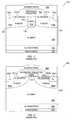
- FIG. 1shows a cross-section view of a portion of a conventional power MOSFET having a buried-gate structure.
- a highly-doped substrate 102forms the drain contact for MOSFET 100 .
- An epitaxial layer 104 formed over substrate 102includes source regions 124 a,b formed in body regions 108 a,b. Body regions 108 a,b are flanked on one side by gate trench 119 . P+ regions 126 a,b form the areas through which contact is made to body regions 108 a,b.
- Gate trench 119is filled with polysilicon forming the MOSFET gate 118 . When MOSFET 100 is turned on, current travels in a vertical direction from source regions 124 a,b along a channel parallel to the sidewalls of gate trench 119 to the backside drain.
- FIG. 2shows a cross-section view of a conventional MOSFET 200 with planar gate structure.
- a highly doped substrate 202forms the drain contact for MOSFET 200 .
- An epitaxial layer 204 formed over substrate 202includes source regions 224 a,b formed in body regions 208 a,b.
- P+ regions 226 a,bform the areas through which contact is made to body regions 208 a,b.
- the MOSFET gate 218is formed on top of the silicon surface instead of being recessed in a trench.
- FIGS. 1 and 2are typically repeated many times to form an array of cells.
- the arraymay be configured in various cellular or stripe layouts known to one skilled in this art.
- These and other types of power deviceshave long been known. Recent advances in semiconductor manufacturing have increased the density (i.e., the number of cells in a given silicon area) of devices. However, the higher density does not necessarily improve power loss in mid to high voltage range (e.g., 60 to 2000 volts) devices. In such devices, the power loss is primarily due to the high resistivity of the drift region (e.g., region 106 in FIG. 1 ). Drift regions have high resistivity because in order for the device to sustain the high voltages during the blocking state, the drift region is lightly doped.
- the high resistivity of the drift regionresults in a higher on-resistance, which in turn results in high power loss. Since a high blocking voltage is a critical feature for mid to high voltage power devices, increasing the drift region doping is not an option. Similar issues are present in power diode devices.
- This dopant inter-diffusionmakes the thermal processing difficult and limits shrinking of the cell pitch.
- the inability to shrink the cell pitchis especially problematic in mid to low voltage devices in which the power loss occurs primarily in the channel region rather than in the drift region.
- the power loss in the channel regionis typically countered by making the cell pitch as small as possible so that a large number of cells can be formed in the same silicon area.
- the columnar opposite polarity regions techniqueis thus unattractive for mid to low voltage devices as it can not be shrunk.
- a semiconductor structureis formed as follows.
- a semiconductor regionis formed to have a P-type region and a N-type region forming a PN junction therebetween.
- a first trench extending in the semiconductor regionis formed adjacent at least one of the P-type and N-type regions is formed. At least one diode is formed in the trench.
- an insulating layer extending along sidewalls of the first trench but being discontinuous along the bottom of the first trenchis formed.
- the semiconductor regionis an epitaxial layer which is formed over and in contact with a substrate.
- the epitaxial layerhas the same conductivity type as the substrate.
- a body regionis formed in the epitaxial layer.
- the body regionis one of the P-type and N-type regions and the other one of the P-type and N-type regions forms a drift region.
- the diodeis arranged in the first trench such that when the semiconductor structure is biased in a blocking state an electric field induced in the at least one diode influences an electric field in the drift region to thereby increase the blocking voltage of the semiconductor structure.
- FIGS. 1 and 2show cross-section views of two conventional MOSFET structures
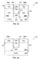
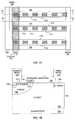
- FIGS. 3A and 3Bshow cross-section views of two embodiments of the trench structure in accordance with the present invention.
- FIGS. 3C-3Dare top views of three exemplary layout designs of the structures shown in FIGS. 3A and 3B ;
- FIGS. 4-6show cross-section views of three exemplary vertical MOSFET structures having diode trenches in accordance with the present invention
- FIGS. 7A, 7B , and 7 Crespectively show a top view, a cross-section view along 7 B- 7 B line in FIG. 7A , and a cross section view along 7 C- 7 C line in FIG. 7A of a lateral MOSFET structure having diode trenches in accordance with the present invention
- FIG. 8shows a cross-section view of a rectifier having diode trenches in accordance with the present invention.
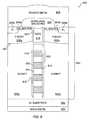
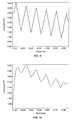
- FIGS. 9 and 10are graphs respectively showing the electric field through diode trenches and drift regions of an exemplary embodiment of the FIG. 4 MOSFET structure.
- Embodiments of a trench having one or more diodes embedded therein and methods of forming the sameare described in accordance with the invention.
- the diode trench structurecan be used in semiconductor devices required to withstand high voltages.
- the diode trenchhelps achieve high current capability, high breakdown voltage, low forward voltage drop, and a small cell pitch.
- FIG. 3Ashows a cross-section view of a semiconductor structure 300 having a trench 310 in accordance with one embodiment of the present invention.
- An epitaxial layer 304is formed over and is of the same conductivity type as a substrate 302 . Regions 308 a,b of opposite conductivity type to epitaxial layer 304 is formed along a top portion of epitaxial layer 304 .
- Trench 310extends from a top surface of epitaxial layer 304 through to substrate 310 .
- Trench 310may alternatively be terminated at a shallower depth (i.e., within regions 306 a,b of epitaxial layer 304 .)
- Trench 310includes a diode made up of opposite conductivity type regions 312 and 314 forming a PN junction 313 therebetween.
- Doped polysilicon or N-type and P-type siliconmay be used to form regions 312 and 314 .
- Other material suitable for forming such diodee.g., Silicon Carbide, Gallium Arsenide, Silicon Germanium may also be used.
- Insulating layer 316extending along the trench sidewalls insulates the diode in the trench from regions 306 a,b and P 308 a,b in epitaxial layer 304 .
- Oxidemay be used as insulating layer 316 . As shown, there is no insulating layer along the bottom of the trench thus allowing the bottom region 312 of the trench diode to be in electrical contact with the underlying substrate 302 . In one embodiment, similar considerations to those dictating the design and manufacture of the gate oxide of MOS transistors are applied in designing and forming insulating layer 316 .
- the thickness of insulating layer 316is determined by such factors as the voltage that insulating layer 316 is required to sustain and the extent to which the electric field in the trench diode is to be induced in regions 306 a,b (i.e., the extent of coupling through the insulating layer).
- regions 312 and 314 in trench 310are shown to be N-type and P-type respectively, their conductivity type may be reversed. Also, either of regions 312 and 314 may be independently biased if desired by, for example, extending one or both regions along the third dimension (i.e., perpendicular to the page) and then up to the silicon surface where contact can be made to them. Although only two regions of opposite conductivity is shown in trench 310 , three regions forming an NPN or PNP stack, or any number of regions of alternating conductivity may be formed in trench 310 . Further, multiple trenches may be used as needed. Substrate 302 and regions 306 a,b are shown to be of N-type conductivity and regions 308 a,b of P-type conductivity. Alternatively, these regions may be of opposite conductivity type as shown in the parentheses in FIG. 3A .
- Structure 300may be incorporated in any power device such as a power MOSFET or a power diode.
- PN junction 307when the device is biased to be in the blocking state (e.g., when a MOSFET is turned off, or a diode is reverse biased), PN junction 307 is reverse biased and is required to sustain high voltages.
- the electric fieldis highest at junction 307 and linearly reduces in N-type region 306 a,b and P-type 308 a,b in the direction away from junction 307 at a rate dictated by the doping concentration of the P-type and N-type regions.
- the diode embedded in trench 310similar to PN junction 307 , is reverse biased and thus the electric field is highest at the diode junction 313 .
- the electric field in the trench diodeinduces a corresponding electric field in N-type regions 306 a,b.
- the induced fieldis manifested in N-type regions 306 a,b in the form of an up-swing spike and a general increase in the electric field curve in N-type regions 306 a,b. This increase in the electric field results in a larger area under the electric field curve which in turn results in a higher breakdown voltage.
- N-type regions 306 a,bWhen structure 300 is biased in the conduction state (e.g., when a MOSFET is turned on or a diode device is forward biased) current passes through N-type regions 306 a,b.
- junction 107In conventional structures such as structure 100 in FIG. 1 , during the conduction state, junction 107 is reverse biased and the amount of charge in the corresponding depletion region linearly decreases from junction 107 toward the edge of the depletion region in N-type region 106 .
- the electric filed across the reverse-biased trench diodeinfluences the charge distribution in N-type regions 306 a,b such that a more uniform charge spreading is obtained in N-type regions 306 a,b.
- the amount of charge in the depletion regionremains relatively uniform across N-type regions 306 a,b.
- the silicon area taken up by N-type regions 306 a,bis more efficiently used.
- the portion of the device on-resistance attributable to regions 306 a,bis, in effect, reduced. This enables reducing the cell pitch for the same on-resistance.
- diode trench 310enables optimizing structure 300 to have higher breakdown voltage, lower on-resistance, and smaller cell pitch than can be achieved by conventional techniques.
- a method of forming structure 300 in accordance with one embodiment of the inventionis as follows.
- An epitaxial layer 304is formed over substrate 302 using conventional methods.
- a blanket P-well implantis carried out in accordance with known implant techniques.
- An anneal stepmay be carried out to drive the P-well deeper into epitaxial layer 304 and to activate the P dopants.
- a trench mask defining a trench openingis then formed by depositing and patterning a photoresist layer. Silicon is removed from the defined trench opening to form trench 310 .
- the trench surfacesare then cleaned and a thin layer of thermal oxide is grown inside the deep trenches.
- a thicker (e.g. 200-600 nm) insulating layere.g., CVD oxide) is then deposited over the thin layer of thermal oxide.
- the sidewalls of the trenchare thus coated with an insulating layer.
- the insulating material along the bottom of the trenchis then removed.
- a suitable spacer materiale.g., nitride
- the diodeis formed by performing a two step process of polysilicon deposition followed by polysilicon etch for each region of the diode.
- the diodeis formed by performing silicon deposition for each diode region using conventional selective epitaxial growth techniques.
- the steps for forming the diodecan be repeated to form additional diodes in the trench. If a large number of stacked polysilicon diodes is required, a cluster tool commonly used to combine the steps of polysilicon deposition and polysilicon etch may be used to speed up the processing time.
- the process stepsare reversed in that the diode trench is formed first (using the same steps outlined above) and then the P-well is formed (using the same process steps outlined above).
- the trench diode's advantageous impact on charge spreading in N-type regions 306 a,bcan be enhanced.
- Two factors impacting the charge spreadingare the avalanche breakdown voltage of the trench diode and the width of the depletion region in the trench diode.
- a high avalanche breakdown voltagecan be obtained so that a maximum electric field of much greater magnitude than the conventional 2 ⁇ 10 5 V/cm can be obtained.
- the only limitation in obtaining the maximum electric fieldthen becomes the ability of insulating layer 316 to withstand high voltages. This limitation can however be eliminated by the proper design of insulating layer 316 .
- Typical gate oxide layershave a maximum electric field exceeding 3.5 ⁇ 10 5 V/cm which suffices for many high voltage applications.
- trench 310is terminated at a shallower depth within (e.g., in the middle of) N-type region 306 .
- P-type region 314fills the entire trench.
- a diodeis not embedded within the trench, a diode is nevertheless formed by P-type region 314 and the underlying N-type region 306 . During operation, this diode influences N-type region 306 in a similar manner to the diode embedded in the FIG. 3A trench 310 .
- the spacings and trench diode arrangementcan be implemented in various stripe or cellular designs.
- a top view of three exemplary designsis shown in FIGS. 3C, 3D , and 3 E.
- trenches 310 care offset from one another
- FIG. 3Eshows trenches 310 e to be aligned and arranged along rows and columns.
- horizontally-extending diode trenches 310 dare arranged as parallel stripes.
- Diode regions 314 d insulated from one another by insulating material 316 dare laterally spaced from each other in each trench stripe 310 d.
- trench regions and the diode regions embedded thereinare shown as square or rectangular shaped regions, they may be designed as circular, oval, hexagonal, or any other geometric shape that is desired. Thus, many different designs, configurations, and geometric shapes can be envisioned by one skilled in the art in light of this disclosure.
- FIG. 4shows a cross-section view of a dual-trench MOSFET 400 in accordance with an embodiment of the present invention.
- a highly-doped substrate 402forms the drain contact for MOSFET 400 .
- An epitaxial layer 404 formed over substrate 402includes source regions 424 a,b formed in body regions 408 a,b.
- Body regions 408 a,bare flanked by gate trench 419 on one side and diode trenches 410 a,b on the other.
- P+ regions 426 a,bform the areas through which contact is made to body regions 408 a,b.
- the portion of epitaxial layer 404 bounded by diode trenches 410 a,b along the sides, body regions 408 a,b and gate trench 419 along the top, and substrate 402 along the bottomforms drift region 406 .
- the gate structureis similar to the gate structure in the prior art FIG. 1 structure 100 .
- Metal layer 428extends along the top and makes contact with sources 424 a,b, P+ regions 426 a,b, and the top of diode trenches 410 a,b, but is isolated from gate 418 by insulating layer 422 .
- Metal layer 430makes contact to substrate 402 along the bottom and forms the drain electrode.
- Diode trenches 410 a,bextend from the top surface of epitaxial layer 404 to the bottom of drift region 406 .
- Diode trenches 410 a,binclude a stack of alternating P-type region 412 and N-type region 414 forming a number of serially-connected diodes 432 .
- the trench diodesare insulated from drift region 406 by an insulating layer 416 extending along the trench sidewalls. Insulating layer 416 however, is discontinuous along the bottom of diode trenches 410 a,b to allow the bottom-most region in the diode trenches to make electrical contact with its underlying region (e.g., with drift region 406 or substrate 402 ).
- the diodes in trenches 410 a,bare reverse-biased during MOSFET operation. In the FIG. 4 implementation, this is achieved by connecting the top-most region in trenches 410 a,b to the source and the bottom-most region to the drain. Alternatively, the top-most region may be connected to a low potential (e.g., ground) separate from the source or even allowed to float, and the bottom-most region may be connected to a high potential separate from the drain. Generally, reverse biasing of the diodes can be achieved by connecting any of the N-type regions in the diode trenches to a high potential, or alternatively connecting any of the P-type regions in the trenches to a low potential.
- a low potentiale.g., ground
- any one or more of the P-type and N-type regions in the diode trenchescan be independently biased by, for example, extending the one or more regions along the third dimension (i.e., perpendicular to the page) and then up to the silicon surface where contact can be made to them.
- FIGS. 9 and 10The graphs in FIGS. 9 and 10 are obtained from simulation results, and show the electric field curve through diode trenches 410 a,b and drift zone 406 of an exemplary MOSFET similar in structure to MOSFET 400 , respectively.
- the vertical axis in FIGS. 9 and 10represents electric field and the horizontal axis represents dimension. In FIG. 9 , the horizontal axis from left to right corresponds to the vertical dimension through the diode trench from top to bottom.
- FIG. 9the horizontal axis from left to right corresponds to the vertical dimension through the diode trench from top to bottom.
- the horizontal axis from left to rightcorresponds to the vertical dimension from body-drift junction 407 to the drift-substrate junction.
- the following tablesets forth the values used for some of the simulation parameters. These values are merely exemplary and not intended to be limiting.
- Parameter ValueEpi doping 2 ⁇ 10 15 cm ⁇ 3 Diode doping (N-type and P-type) 1 ⁇ 10 16 cm ⁇ 3 Thickness t 1 of each of the N-type and P- 0.5 ⁇ m type regions in diode trenches Thickness of oxide along trench sidewalls 500 ⁇ Thickness of gate oxide 500 ⁇
- the reverse-bias across the trench diodesresults in an electric field peak at each diode junction (e.g., junction 413 ) as expected.
- Each of these electric field peaksinduces a corresponding electric filed increase (peak) in a corresponding area of drift region 406 as shown in the FIG. 10 graph.
- An almost square-shaped area under the electric field curveis thus obtained ( FIG. 10 ), which is substantially greater than the area under the triangular-shaped curve for conventional MOSFET structures.
- a substantial increase in the breakdown voltageis achieved.
- the larger the number of diodes embedded in the trenchthe greater would be the number of peaks in the electric filed in the drift region, and thus the higher would be the area under the curve.
- the higher breakdown voltageenables the doping concentration of drift region 406 (conventionally kept low to obtain the necessary breakdown voltage) to be increased to reduce the on-resistance, if desired.
- the electric field across the trench diodesinfluences the charge distribution in drift region 406 such that a more uniform charge spreading is obtained in drift region 406 .
- the uniform charge spreadingresults in a more efficient use of the drift region silicon area.
- the cell pitch of the FIG. 4 structurecan be made smaller.
- the width of the diode trenchescan be made as small as the process technology allows to minimize its impact on the cell pitch.
- a method of forming structure 400 in accordance with one embodiment of the inventionis as follows. Conventional process steps are carried out to form the buried gate structure 419 , including source regions 424 a,b, body regions 408 a,b, and P+ regions 426 a,b, in epitaxial layer 404 . Alternatively, the process steps outlined in the above-referenced U.S. patent application (Ser. No. 08/970,221, titled “Field Effect Transistor and Method of its Manufacture”), commonly assigned, may be carried out to form the gate structure. Next, the same process steps and variations thereof described above in connection with forming trench 310 ( FIG. 3A ) and the diode embedded therein may be used to form deep trenches 410 a,b and the multiple diodes embedded in them.
- diode trenches 410 a,b, body regions 408 a,b, and gate trench 419are formed is not limited to a particular sequence.
- an alternate sequence to that described aboveis: form the diode trenches first, the body regions second, and the gate trench third.
- Another sequenceis: form the gate trench first, the body regions second, and the diode trenches third. Accordingly, there are six possible sequence permutations, any one of which may be used.
- FIG. 5shows a cross-section view of a MOSFET structure 500 in accordance with another embodiment of the present invention.
- a highly-doped substrate 502forms an ohmic drain contact.
- An epitaxial layer 504 formed over substrate 502includes source regions 524 a,b formed in body regions 508 a,b.
- Body regions 508 a,bare each flanked on one side by diode trenches 510 a,b.
- P+ regions 526 a,bform the areas through which contact is made to body regions 508 a,b.
- the portion of epitaxial layer 504 bounded by diode trenches 510 a,b along the sides, body regions 508 a,b and gate 518 along the top, and substrate 502 along the bottomforms drift region 506 .
- the gate structureis planar similar to that shown in the FIG. 2 prior art structure 200 .
- Metal layer 528extends along the top and makes contact with sources region 524 a,b, P+ regions 526 a,b, and the top of trenches 510 a,b, but is isolated from gate 518 by insulating layer 522 .
- Metal layer 530makes contact to substrate 502 along the bottom, forming the drain electrode.
- Trenches 510 a,bextend from the top surface of epitaxial layer 504 to the bottom of drift region 506 .
- Diode trenches 510 a,bare similar in structure to those in the FIG. 4 structure, and as such the same discussions provided above in connection with the FIG. 4 trench structure applies here.
- the trench diodesare insulated from drift region 506 by insulating layer 516 extending along the trench sidewalls. Insulating layer 516 however, is discontinuous along the bottom of the diode trenches so that the bottom-most region in the trenches makes electrical contact with its underlying region.
- the diodes in trenches 510 a,bare reverse-biased during MOSFET operation. Any one of the same techniques for reverse biasing the diodes in trenches 410 a,b outlined above may be used here.
- MOSFET 500The operation of MOSFET 500 is similar to that of the prior art FIG. 2 structure and thus will not be described.
- Diode trenches 510 a,binfluence the electric field and the charge distribution in drift region 506 in a similar manner to diode trenches 410 a,b ( FIG. 4 ) so that a higher breakdown voltage, lower on-resistance, and smaller cell pitch is obtained as compared to the prior art FIG. 2 structure.
- a method of forming structure 500 in accordance with one embodiment of the inventionis as follows. Conventional process steps are carried out to form the planar gate structure. Deep trenches are then etched in the space between the planar gate structures. The same process steps and variations thereof described above in connection with forming deep trenches 410 a,b ( FIG. 4 ) and the diodes embedded therein may then be carried out to form deep trenches 510 a,b and the diodes embedded therein. In an alternative embodiment, the process steps are reversed in that the deep trenches are formed first (using the same steps outlined above), and then the planar gate structure is formed between the diode trenches (using the same process steps outlined above).
- FIG. 6shows a cross-section view of another MOSFET structure 600 in accordance with another embodiment of the present invention.
- MOSFET gate 618 and trench diodes 632are advantageously embedded in one trench 610 rather than two as in the FIG. 4 structure 400 . This yields a highly compact cell structure while the same breakdown voltage and on-resistance improvements of prior embodiments are maintained.
- a highly-doped substrate 602forms the drain contact.
- An epitaxial layer 604 formed over substrate 602includes source regions 624 a,b formed in body regions 608 a,b.
- P+ regions 626 a,bform the areas through which contact is made to body regions 608 a,b.
- Body regions 608 a,bare separated by trench 610 .
- the portions of epitaxial layer 604 bounded by body regions 608 a,b, substrate 602 , and trench 610form drift regions 606 a,b.
- the structural relation between gate 618 and the source, body regionsis similar to those in the FIG. 4 structure.
- Trench 610extends from the top surface of epitaxial layer 604 to the bottom of drift regions 606 a,b.
- the lower section of trench 610 wherein the diodes are embeddedis similar in structure to diode trenches 410 a,b ( FIG. 4 ), and as such the same discussions provided above in connection with the structure of trenches 410 a,b applies here.
- the diodes embedded in trench 610are insulated from drift regions 606 a,b by insulating layer 616 extending along the trench sidewalls. Insulating layer 616 however, is discontinuous along the bottom of the trench to allow the bottom-most region in the trench to make contact with its underlying region.
- Insulating layer 616may be the same as or different from gate oxide 620 . Generally, insulating layer 616 needs to withstand the high voltage between the trench diode regions and drift regions 606 a,b. Metal layer 628 extends along the top and makes contact to sources 624 a,b and P+ regions 626 a,b, but is insulated from gate 618 by insulating layer 622 .
- the diodes in trench 610are reverse-biased during MOSFET operation. Any one of the same techniques for reverse biasing the diodes in trenches 410 a,b outlined above may be used here.
- Diode trench 610influences the electric field and the charge distribution in drift regions 606 a,b in a similar manner to diode trenches 410 a,b ( FIG. 4 ) so that a high breakdown voltage, low on-resistance, and small cell pitch are obtained.
- a method of forming structure 600 in accordance with one embodiment of the inventionis as follows.
- An epitaxial layer 604is formed over substrate 302 using conventional methods.
- a blanket P-well implantis carried out in accordance with known implant techniques to form a P-well.
- An anneal stepmay be carried out to drive the P-well deeper into epitaxial layer 604 and to activate the P dopants.
- a trench mask defining a trench openingis then formed by depositing and patterning a photoresist layer. Silicon is removed from the defined trench opening to form trench 610 .
- the trench surfacesare then cleaned and a thin layer of thermal oxide is grown inside the deep trenches.
- a thickere.g.
- insulating layere.g., CVD oxide
- thermal oxidee.g., silicon dioxide
- a suitable spacer materiale.g., nitride may be used to protect the insulating material along the trench sidewalls during removal of insulation material at the trench bottom.
- insulating layers 616 and 620results in insulating layers 616 and 620 to be the same, modifying the process steps so that these two insulating layers are different would be obvious to one skilled in this art.
- the same process steps and variations thereof described above in connection with forming the diode in trench 310may be used to form the multiple diodes shown in trench 610 .
- an insulating layeris formed over the top of the diode structure.
- Gate 618is then embedded in trench 610 using conventional methods.
- the process stepsare reversed in that the deep trench is formed first (using the same steps outlined above) and then body regions 608 a,b are formed.
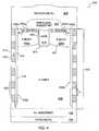
- FIG. 7Ashows a top view partial-layout diagram of a lateral MOSFET structure having diode trenches in accordance with the present invention.
- FIGS. 7B and 7Cshow cross-section views across 7 B- 7 B and 7 C- 7 C lines in FIG. 7A , and will be used together with the FIG. 7A top view to describe the structure of and method of forming the lateral MOSFET.
- both source region 724 and drain region 760are formed along the same surface as opposed to two opposing surfaces as in the vertical structures. Thus, the current conduction occurs laterally along the top surface, hence “lateral MOSFET”.
- FIG. 7Ashows a top view partial-layout diagram of a lateral MOSFET structure having diode trenches in accordance with the present invention.
- FIGS. 7B and 7Cshow cross-section views across 7 B- 7 B and 7 C- 7 C lines in FIG. 7A , and will be used together with the FIG. 7A top view to describe the structure of and method of forming the
- trenches 710are shown extending from drain region 760 to source region 724 through drift region 706 and body region 708 .
- a number of P-type and N-type regionsare alternately arranged adjacent one another forming a number of serially-connected diodes in each trench 710 .
- the P-type and N-type regionsare insulated from the drift region 706 and body region 706 by an insulating layer 716 extending along the bottom and sidewalls of trenches 710 . Insulating layer 716 however does not extend along the trench sidewalls at the lateral ends of the trenches where they terminate in drain region 760 and body region 708 . This allows the last diode region on each end of each trench to make electrical contact with its adjacent region (i.e., with drain region 760 on the right side and with source region 724 on the left side).
- Line 7 B- 7 Bextends through the channel region, and the corresponding cross-section view shown in FIG. 7B is similar to that for conventional lateral MOSFET structures. The operation of this structure is thus similar to conventional lateral MOSFETs.
- Line 7 C- 7 Cextends through one of the trenches 710 , and the corresponding cross-section view is shown in FIG. 7C .
- An epitaxial layer 704 formed over substrate 702includes body region 708 and drain region 760 .
- P+ region 726(the area through which ohmic contact is made to body region 708 ) and source region 724 are formed in body region 708 .
- the portion of epitaxial layer 704 below and between body region 708 and drain regionforms drift region 706 .
- the gate structureis planar and is similar to that in conventional lateral MOSFETs except that gate 718 also extends over portions of diode trenches 710 as shown in FIG. 7A .
- Metal layer 728makes contact with source region 724 and P+ region 726 but is isolated from gate 718 by insulating layer 722 .
- Metal layer 730makes contact to drain region 760 .
- the diodes in trenches 710are reverse-biased during operation. This is achieved by having the right-most region in trenches 710 in contact with drain region 760 and the left-most region in contact with source region 724 .
- the left-most regionmay be insulated from source region 724 and then connected to a low potential (e.g., ground) or even allowed to float.
- the right-most regionmay be connected to a high potential separate from the drain.
- reverse biasing of the diodescan be achieved by connecting any of the N-type regions in the diode trenches to a high potential, or alternatively connecting any of the P-type regions in the trenches to a low potential.
- diode trenches 710influence the electric field and the charge distribution in drift region 706 in a similar manner to diode trenches 410 a,b ( FIG. 4 ) so that a higher breakdown voltage, lower on-resistance, and smaller cell pitch is obtained as compared to the conventional lateral MOSFET structures.
- FIGS. 7A-7Cshow diode trenches 710 abutting source region 724 , these trenches may alternatively terminate in body region 708 near the body-drift junction. This however requires that the left-most diode region be of the same conductivity type as body region 708 to eliminate any breakdown issues at the junction between the body region and the left-most diode region.
- insulating layer 716may be extended along the left-end sidewall of the trenches so that the left-most diode region in the trenches is insulated from the source and body regions.
- insulating layer 716may be formed along all four sidewalls of the trenches so that the diodes are completely insulated on all sides.
- accessbe provided to at least one of the diode regions in each trench so that the diodes can be reverse biased during operation.
- Such accessmay be provided along the top side of the structure by creating one or more openings in the insulating layer 722 and electrically contacting one or more of the diode regions in the trench.
- a method of forming the lateral MOSFET structure shown in FIGS. 7A-7C in accordance with one embodiment of the inventionis as follows.
- An epitaxial layer 704is formed over substrate 702 using conventional methods.
- a trench mask defining trench openingsis then formed by depositing and patterning a photoresist layer. Silicon is removed from the defined trench openings to form trenches in the epitaxial layer. The trench surfaces are then cleaned and a thin layer of thermal oxide is grown inside the deep trenches.
- a thicker (e.g. 200-600 nm) insulating layere.g., CVD oxide
- CVD oxidee.g., CVD oxide
- the insulating material along two sidewallsare removed.
- a suitable spacer materiale.g., nitride
- polysiliconis first deposited and then a planarization etch is carried out so that only those portions of the polysilicon filling the trenches remain. If the deposited polysilicon is doped polysilicon, a masking and implanting sequence of steps is carried out to form the diodes (i.e., to form alternating regions of opposite conductivity). If the deposited polysilicon is undoped, then the masking and implanting sequence of steps need to be carried out twice to create the regions of opposite conductivity.
- siliconis deposited in the trenches followed by one or two sets of masking and implanting sequence of steps (depending on whether the deposited silicon is doped) to create the alternating regions of opposite conductivity type.
- the gate oxide and the overlying gateare formed in accordance with conventional methods.
- a blanket P-well implantis carried out in accordance with known implant techniques to form a P-well.
- An anneal stepmay be carried out to drive the P-well deeper into epitaxial layer 304 and to activate the P dopants.
- Source region 724 , drain region 760 , and P+ region 726 , insulating layer 722 , and metal layers 728 and 730are then formed in accordance with conventional methods.
- a buried layeris formed between substrate 702 and drift region 706 , wherein the buried layer has a conductivity type opposite that of the substrate and drift region.
- the lateral MOSFET structureis formed using silicon-on-insulator (SOI) technology. In this embodiment, an insulating layer would be present between drift region 706 and substrate 702 .
- FIG. 8shows a cross-section view of a power diode device 800 in accordance with an embodiment of the present invention.
- a highly-doped substrate 802forms the cathode contact.
- An epitaxial layer 804 formed over substrate 802includes P-well regions 808 each being flanked on the sides by trenches 810 .
- the regions of epitaxial layer 804 bounded by trenches 810 along the sides, P-well regions 808 along the top, and substrate 802 along the bottomform drift regions 806 .
- Metal layer 828makes contact to P-well regions 808 and the top surface of trenches 810 , and forms the anode electrode.
- Metal layer 830extends along the bottom and makes contact to substrate 802 , forming the cathode electrode.
- Trenches 810extend from the top surface of epitaxial layer 804 to the bottom of drift region 806 .
- Trenches 810are similar in structure to trenches 410 a,b ( FIG. 4 ), and as such the same discussions provided above in connection with trenches 410 a,b apply here.
- the diodes in trenches 810are insulated from P-well regions 808 and drift regions 806 by insulating layer 816 extending along the trench sidewalls. Insulating layer 816 however, is discontinuous along the bottom of the trenches so that the bottom-most region in the trenches makes electrical contact with its underlying region.
- the diodes in trenches 810are reverse-biased during device operation. Any one of the same techniques for reverse biasing the diodes in trenches 410 a,b outlined above may be used to ensure that the diodes in trenches 810 are reverse-biased during operation.
- Trenches 810influence the electric field and the charge distribution in drift regions 806 in a similar manner to diode trenches 410 a,b ( FIG. 4 ) so that a higher breakdown voltage, lower on-resistance, and smaller cell pitch is obtained as compared to conventional power diodes.
- the same process steps and variations thereof described above in connection with forming structure 300 ( FIG. 3 )may be used to form structure 800 .
- the structure and method of the present inventioncan be used to implement mid to low voltage (e.g., ⁇ 200V) devices.
- mid to low voltagee.g., ⁇ 200V
- the majority of lossesoccur in the channel region.
- the present inventionlends itself well to implementing mid to low voltage devices in that the cell pitch can be substantially reduced (as described above) so that a larger number of cells can be formed in a give silicon area, and thus the losses in the channel region are reduced.
- FIGS. 4, 5 , 7 , and 8While the above is a complete description of the embodiments of the present invention, it is possible to use various alternatives, modifications and equivalents.
- only one regionmay be used in the portion of the diode trench(es) extending from the side of the trench closest to the source region to the vicinity of the edge of the drift-body junction.
- the top three regions in the diode trench(es)may be replaced with one elongated P-type or N-type region.
- an insulating materiale.g., oxide
- the number of processing steps associated with forming the diodes in the trench(es)is reduced without adversely impacting the performance of the different structures.
- the diode trench(es) in FIGS. 4-6 and 8may be terminated at a shallower depth within (e.g., in the middle of) the drift region if desired.
- the diode trenchesmay be terminated within epitaxial layer 706 rather than extend all the way to drain region 760 .
- the cross-section views of the different embodimentsmay not be to scale, and as such are not intended to limit the possible variations in the layout design of the corresponding structures. Therefore, the scope of the present invention should be determined not with reference to the above description but should, instead, be determined with reference to the appended claim, along with their full scope of equivalents.
Landscapes
- Metal-Oxide And Bipolar Metal-Oxide Semiconductor Integrated Circuits (AREA)
Abstract
Description
- This application is a division of U.S. application Ser. No. 10/288,982, filed Nov. 5, 2002, which is incorporated by reference in its entirety for all purposes.
- The present invention relates in general to semiconductor technology and in particular to high-voltage semiconductor structures and methods of manufacturing the same.
FIG. 1 shows a cross-section view of a portion of a conventional power MOSFET having a buried-gate structure. A highly-dopedsubstrate 102 forms the drain contact forMOSFET 100. Anepitaxial layer 104 formed oversubstrate 102 includessource regions 124a,bformed inbody regions 108a,b.Body regions 108a,bare flanked on one side bygate trench 119.P+ regions 126a,bform the areas through which contact is made tobody regions 108a,b.Gate trench 119 is filled with polysilicon forming theMOSFET gate 118. WhenMOSFET 100 is turned on, current travels in a vertical direction fromsource regions 124a,balong a channel parallel to the sidewalls ofgate trench 119 to the backside drain.FIG. 2 shows a cross-section view of aconventional MOSFET 200 with planar gate structure. A highly dopedsubstrate 202 forms the drain contact forMOSFET 200. Anepitaxial layer 204 formed oversubstrate 202 includessource regions 224a,bformed inbody regions 208a,b.P+ regions 226a,bform the areas through which contact is made tobody regions 208a,b.The MOSFET gate218 is formed on top of the silicon surface instead of being recessed in a trench. WhenMOSFET 200 is turned on, current flows fromsource regions 224a,balong a channel beneathgate 118 and then vertically throughdrift region 206 to the backside drain.- The structures shown in
FIGS. 1 and 2 are typically repeated many times to form an array of cells. The array may be configured in various cellular or stripe layouts known to one skilled in this art. These and other types of power devices have long been known. Recent advances in semiconductor manufacturing have increased the density (i.e., the number of cells in a given silicon area) of devices. However, the higher density does not necessarily improve power loss in mid to high voltage range (e.g., 60 to 2000 volts) devices. In such devices, the power loss is primarily due to the high resistivity of the drift region (e.g.,region 106 inFIG. 1 ). Drift regions have high resistivity because in order for the device to sustain the high voltages during the blocking state, the drift region is lightly doped. The high resistivity of the drift region results in a higher on-resistance, which in turn results in high power loss. Since a high blocking voltage is a critical feature for mid to high voltage power devices, increasing the drift region doping is not an option. Similar issues are present in power diode devices. - Attempts have been made to improve the device power loss while maintaining a high blocking voltage. In one approach, columnar opposite polarity regions extending parallel to the current flow are formed between the body-gate structure at the top and the substrate at the bottom. The columnar opposite polarity regions prevent the electric field from decreasing linearly away from the base-drift junction, thus allowing the device to support higher blocking voltages. This technique however depends on charge balance between the conduction and opposite polarity regions and thus requires precise doping control of the opposite polarity regions. The opposite polarity regions are formed before the diffused base and source regions. When the base and source regions are annealed during a thermal cycle, the dopants in the opposite polarity regions undesirably diffuse into each other. This dopant inter-diffusion makes the thermal processing difficult and limits shrinking of the cell pitch. The inability to shrink the cell pitch is especially problematic in mid to low voltage devices in which the power loss occurs primarily in the channel region rather than in the drift region. In the mid to low voltage devices, the power loss in the channel region is typically countered by making the cell pitch as small as possible so that a large number of cells can be formed in the same silicon area. The columnar opposite polarity regions technique is thus unattractive for mid to low voltage devices as it can not be shrunk.
- Thus, a technique which enables achieving a high device blocking capability, low on-resistance, and high current handling capability without preventing the cell pitch to be shrunk is desirable.
- In accordance with an embodiment of the present invention, a semiconductor structure is formed as follows. A semiconductor region is formed to have a P-type region and a N-type region forming a PN junction therebetween. A first trench extending in the semiconductor region is formed adjacent at least one of the P-type and N-type regions is formed. At least one diode is formed in the trench.
- In one embodiment, an insulating layer extending along sidewalls of the first trench but being discontinuous along the bottom of the first trench is formed.
- In one embodiment, the semiconductor region is an epitaxial layer which is formed over and in contact with a substrate. The epitaxial layer has the same conductivity type as the substrate.
- In another embodiment, a body region is formed in the epitaxial layer. The body region is one of the P-type and N-type regions and the other one of the P-type and N-type regions forms a drift region. The diode is arranged in the first trench such that when the semiconductor structure is biased in a blocking state an electric field induced in the at least one diode influences an electric field in the drift region to thereby increase the blocking voltage of the semiconductor structure.
- The following detailed description and the accompanying drawings provide a better understanding of the nature and advantages of the present invention.
FIGS. 1 and 2 show cross-section views of two conventional MOSFET structures;FIGS. 3A and 3B show cross-section views of two embodiments of the trench structure in accordance with the present invention;FIGS. 3C-3D are top views of three exemplary layout designs of the structures shown inFIGS. 3A and 3B ;FIGS. 4-6 show cross-section views of three exemplary vertical MOSFET structures having diode trenches in accordance with the present invention;FIGS. 7A, 7B , and7C respectively show a top view, a cross-section view along7B-7B line inFIG. 7A , and a cross section view along7C-7C line inFIG. 7A of a lateral MOSFET structure having diode trenches in accordance with the present invention;FIG. 8 shows a cross-section view of a rectifier having diode trenches in accordance with the present invention; andFIGS. 9 and 10 are graphs respectively showing the electric field through diode trenches and drift regions of an exemplary embodiment of theFIG. 4 MOSFET structure.- Embodiments of a trench having one or more diodes embedded therein and methods of forming the same are described in accordance with the invention. The diode trench structure can be used in semiconductor devices required to withstand high voltages. The diode trench helps achieve high current capability, high breakdown voltage, low forward voltage drop, and a small cell pitch.
FIG. 3A shows a cross-section view of asemiconductor structure 300 having atrench 310 in accordance with one embodiment of the present invention. Anepitaxial layer 304 is formed over and is of the same conductivity type as asubstrate 302.Regions 308a,bof opposite conductivity type toepitaxial layer 304 is formed along a top portion ofepitaxial layer 304.Trench 310 extends from a top surface ofepitaxial layer 304 through tosubstrate 310. Trench310 may alternatively be terminated at a shallower depth (i.e., withinregions 306a,bofepitaxial layer 304.)Trench 310 includes a diode made up of oppositeconductivity type regions PN junction 313 therebetween. Doped polysilicon or N-type and P-type silicon may be used to formregions - Insulating
layer 316 extending along the trench sidewalls insulates the diode in the trench fromregions 306a,bandP 308a,binepitaxial layer 304. Oxide may be used as insulatinglayer 316. As shown, there is no insulating layer along the bottom of the trench thus allowing thebottom region 312 of the trench diode to be in electrical contact with theunderlying substrate 302. In one embodiment, similar considerations to those dictating the design and manufacture of the gate oxide of MOS transistors are applied in designing and forming insulatinglayer 316. For example, as in gate oxide of MOS transistors, the thickness of insulatinglayer 316 is determined by such factors as the voltage that insulatinglayer 316 is required to sustain and the extent to which the electric field in the trench diode is to be induced inregions 306a,b(i.e., the extent of coupling through the insulating layer). - Although
regions trench 310 are shown to be N-type and P-type respectively, their conductivity type may be reversed. Also, either ofregions trench 310, three regions forming an NPN or PNP stack, or any number of regions of alternating conductivity may be formed intrench 310. Further, multiple trenches may be used as needed.Substrate 302 andregions 306a,bare shown to be of N-type conductivity andregions 308a,bof P-type conductivity. Alternatively, these regions may be of opposite conductivity type as shown in the parentheses inFIG. 3A . Structure 300 may be incorporated in any power device such as a power MOSFET or a power diode. In any of these devices, when the device is biased to be in the blocking state (e.g., when a MOSFET is turned off, or a diode is reverse biased),PN junction 307 is reverse biased and is required to sustain high voltages. As is well-known in this art, under reverse-bias conditions, the electric field is highest atjunction 307 and linearly reduces in N-type region 306a,band P-type 308a,bin the direction away fromjunction 307 at a rate dictated by the doping concentration of the P-type and N-type regions. It is also well known that the larger the area under the electric field curve (i.e., the lower the rate at which the electric field reduces), the greater is the breakdown voltage. During operation, the diode embedded intrench 310, similar toPN junction 307, is reverse biased and thus the electric field is highest at thediode junction 313. Through insulatinglayer 316, the electric field in the trench diode induces a corresponding electric field in N-type regions 306a,b.The induced field is manifested in N-type regions 306a,bin the form of an up-swing spike and a general increase in the electric field curve in N-type regions 306a,b.This increase in the electric field results in a larger area under the electric field curve which in turn results in a higher breakdown voltage.- It can be seen that by using multiple diodes in
trench 310, multiple spikes can be induced along the depth of N-type regions 306a,b(this is explained in more detail in reference toFIGS. 9 and 10 further below). This results in an electric field curve which tapers down from its highest level atjunction 307 at a far lower rate than in conventional structures. An almost square-shaped area can thus be obtained under the electric field curve in N-type regions 306a,bas opposed to the conventional triangular shape. A far greater breakdown voltage can thus be obtained. - When
structure 300 is biased in the conduction state (e.g., when a MOSFET is turned on or a diode device is forward biased) current passes through N-type regions 306a,b.In conventional structures such asstructure 100 inFIG. 1 , during the conduction state,junction 107 is reverse biased and the amount of charge in the corresponding depletion region linearly decreases fromjunction 107 toward the edge of the depletion region in N-type region 106. However, by introducingdiode trench 310, the electric filed across the reverse-biased trench diode influences the charge distribution in N-type regions 306a,bsuch that a more uniform charge spreading is obtained in N-type regions 306a,b.That is, the amount of charge in the depletion region remains relatively uniform across N-type regions 306a,b.By spreading the charge more uniformly in N-type regions 306a,b,the silicon area taken up by N-type regions 306a,bis more efficiently used. Hence, for the same size N-type regions 306a,b,the portion of the device on-resistance attributable toregions 306a,bis, in effect, reduced. This enables reducing the cell pitch for the same on-resistance. - Accordingly,
diode trench 310 enables optimizingstructure 300 to have higher breakdown voltage, lower on-resistance, and smaller cell pitch than can be achieved by conventional techniques. - A method of forming
structure 300 in accordance with one embodiment of the invention is as follows. Anepitaxial layer 304 is formed oversubstrate 302 using conventional methods. A blanket P-well implant is carried out in accordance with known implant techniques. An anneal step may be carried out to drive the P-well deeper intoepitaxial layer 304 and to activate the P dopants. A trench mask defining a trench opening is then formed by depositing and patterning a photoresist layer. Silicon is removed from the defined trench opening to formtrench 310. The trench surfaces are then cleaned and a thin layer of thermal oxide is grown inside the deep trenches. A thicker (e.g. 200-600 nm) insulating layer (e.g., CVD oxide) is then deposited over the thin layer of thermal oxide. The sidewalls of the trench are thus coated with an insulating layer. The insulating material along the bottom of the trench is then removed. A suitable spacer material (e.g., nitride) may be used to protect the insulating material along the trench sidewalls during removal of insulation material at the trench bottom. In the embodiment wherein doped polysilicon is used to form the trench diode, the diode is formed by performing a two step process of polysilicon deposition followed by polysilicon etch for each region of the diode. In the embodiment wherein the trench diode is from silicon material, the diode is formed by performing silicon deposition for each diode region using conventional selective epitaxial growth techniques. The steps for forming the diode can be repeated to form additional diodes in the trench. If a large number of stacked polysilicon diodes is required, a cluster tool commonly used to combine the steps of polysilicon deposition and polysilicon etch may be used to speed up the processing time. - In an alternate embodiment, the process steps are reversed in that the diode trench is formed first (using the same steps outlined above) and then the P-well is formed (using the same process steps outlined above).
- By properly designing the P-type and N-type regions of the trench diode, the trench diode's advantageous impact on charge spreading in N-
type regions 306a,bcan be enhanced. Two factors impacting the charge spreading are the avalanche breakdown voltage of the trench diode and the width of the depletion region in the trench diode. For example, by selecting proper doping concentration for each of the P-type and N-type regions of the trench diode, a high avalanche breakdown voltage can be obtained so that a maximum electric field of much greater magnitude than the conventional 2×10⁵V/cm can be obtained. The only limitation in obtaining the maximum electric field then becomes the ability of insulatinglayer 316 to withstand high voltages. This limitation can however be eliminated by the proper design of insulatinglayer 316. Typical gate oxide layers have a maximum electric field exceeding 3.5×10⁵V/cm which suffices for many high voltage applications. - In another embodiment shown in
FIG. 3B ,trench 310 is terminated at a shallower depth within (e.g., in the middle of) N-type region 306. P-type region 314 fills the entire trench. In this embodiment, although a diode is not embedded within the trench, a diode is nevertheless formed by P-type region 314 and the underlying N-type region 306. During operation, this diode influences N-type region 306 in a similar manner to the diode embedded in theFIG. 3A trench 310. - The spacings and trench diode arrangement can be implemented in various stripe or cellular designs. A top view of three exemplary designs is shown in
FIGS. 3C, 3D , and3E. InFIG. 3C ,trenches 310care offset from one another, whileFIG. 3E showstrenches 310eto be aligned and arranged along rows and columns. InFIG. 3D , horizontally-extendingdiode trenches 310dare arranged as parallel stripes.Diode regions 314dinsulated from one another by insulatingmaterial 316dare laterally spaced from each other in eachtrench stripe 310d.Although the trench regions and the diode regions embedded therein are shown as square or rectangular shaped regions, they may be designed as circular, oval, hexagonal, or any other geometric shape that is desired. Thus, many different designs, configurations, and geometric shapes can be envisioned by one skilled in the art in light of this disclosure. FIG. 4 shows a cross-section view of a dual-trench MOSFET 400 in accordance with an embodiment of the present invention. A highly-dopedsubstrate 402 forms the drain contact forMOSFET 400. Anepitaxial layer 404 formed oversubstrate 402 includessource regions 424a,bformed inbody regions 408a,b.Body regions 408a,bare flanked bygate trench 419 on one side anddiode trenches 410a,bon the other.P+ regions 426a,bform the areas through which contact is made tobody regions 408a,b.The portion ofepitaxial layer 404 bounded bydiode trenches 410a,balong the sides,body regions 408a,bandgate trench 419 along the top, andsubstrate 402 along the bottom forms driftregion 406. The gate structure is similar to the gate structure in the prior artFIG. 1 structure 100.Metal layer 428 extends along the top and makes contact withsources 424a,b,P+ regions 426a,b,and the top ofdiode trenches 410a,b,but is isolated fromgate 418 by insulatinglayer 422.Metal layer 430 makes contact tosubstrate 402 along the bottom and forms the drain electrode.Diode trenches 410a,bextend from the top surface ofepitaxial layer 404 to the bottom ofdrift region 406.Diode trenches 410a,binclude a stack of alternating P-type region 412 and N-type region 414 forming a number of serially-connecteddiodes 432. The trench diodes are insulated fromdrift region 406 by an insulatinglayer 416 extending along the trench sidewalls. Insulatinglayer 416 however, is discontinuous along the bottom ofdiode trenches 410a,bto allow the bottom-most region in the diode trenches to make electrical contact with its underlying region (e.g., withdrift region 406 or substrate402).- The diodes in
trenches 410a,bare reverse-biased during MOSFET operation. In theFIG. 4 implementation, this is achieved by connecting the top-most region intrenches 410a,bto the source and the bottom-most region to the drain. Alternatively, the top-most region may be connected to a low potential (e.g., ground) separate from the source or even allowed to float, and the bottom-most region may be connected to a high potential separate from the drain. Generally, reverse biasing of the diodes can be achieved by connecting any of the N-type regions in the diode trenches to a high potential, or alternatively connecting any of the P-type regions in the trenches to a low potential. Any one or more of the P-type and N-type regions in the diode trenches can be independently biased by, for example, extending the one or more regions along the third dimension (i.e., perpendicular to the page) and then up to the silicon surface where contact can be made to them. - The operation of
vertical MOSFET 400 is similar to that of the prior artFIG. 1 and thus will not be described. However, the advantageous impact ofdiode trenches 410a,bon the performance characteristics ofMOSFET 400 is described next using the graphs inFIGS. 9 and 10 . The graphs inFIGS. 9 and 10 are obtained from simulation results, and show the electric field curve throughdiode trenches 410a,banddrift zone 406 of an exemplary MOSFET similar in structure toMOSFET 400, respectively. The vertical axis inFIGS. 9 and 10 represents electric field and the horizontal axis represents dimension. InFIG. 9 , the horizontal axis from left to right corresponds to the vertical dimension through the diode trench from top to bottom. InFIG. 10 , the horizontal axis from left to right corresponds to the vertical dimension from body-drift junction 407 to the drift-substrate junction. The following table sets forth the values used for some of the simulation parameters. These values are merely exemplary and not intended to be limiting.Parameter Value Epi doping 2 × 1015 cm−3 Diode doping (N-type and P-type) 1 × 1016 cm−3 Thickness t1of each of the N-type and P- 0.5 μm type regions in diode trenches Thickness of oxide along trench sidewalls 500 Å Thickness of gate oxide 500 Å - As shown in the
FIG. 9 graph, the reverse-bias across the trench diodes results in an electric field peak at each diode junction (e.g., junction413) as expected. Each of these electric field peaks induces a corresponding electric filed increase (peak) in a corresponding area ofdrift region 406 as shown in theFIG. 10 graph. An almost square-shaped area under the electric field curve is thus obtained (FIG. 10 ), which is substantially greater than the area under the triangular-shaped curve for conventional MOSFET structures. Thus, a substantial increase in the breakdown voltage is achieved. The larger the number of diodes embedded in the trench, the greater would be the number of peaks in the electric filed in the drift region, and thus the higher would be the area under the curve. The higher breakdown voltage enables the doping concentration of drift region406 (conventionally kept low to obtain the necessary breakdown voltage) to be increased to reduce the on-resistance, if desired. - As described above in reference to the structure in
FIG. 3A , during the on state ofMOSFET 400, the electric field across the trench diodes influences the charge distribution indrift region 406 such that a more uniform charge spreading is obtained indrift region 406. The uniform charge spreading results in a more efficient use of the drift region silicon area. Thus, for the same on-resistance of, for example, the prior artFIG. 1 structure, the cell pitch of theFIG. 4 structure can be made smaller. The width of the diode trenches can be made as small as the process technology allows to minimize its impact on the cell pitch. - A method of forming
structure 400 in accordance with one embodiment of the invention is as follows. Conventional process steps are carried out to form the buriedgate structure 419, includingsource regions 424a,b,body regions 408a,b,andP+ regions 426a,b,inepitaxial layer 404. Alternatively, the process steps outlined in the above-referenced U.S. patent application (Ser. No. 08/970,221, titled “Field Effect Transistor and Method of its Manufacture”), commonly assigned, may be carried out to form the gate structure. Next, the same process steps and variations thereof described above in connection with forming trench310 (FIG. 3A ) and the diode embedded therein may be used to formdeep trenches 410a,band the multiple diodes embedded in them. - Generally, the order in which
diode trenches 410a,b,body regions 408a,b,andgate trench 419 are formed is not limited to a particular sequence. For example, an alternate sequence to that described above is: form the diode trenches first, the body regions second, and the gate trench third. Another sequence is: form the gate trench first, the body regions second, and the diode trenches third. Accordingly, there are six possible sequence permutations, any one of which may be used. FIG. 5 shows a cross-section view of aMOSFET structure 500 in accordance with another embodiment of the present invention. A highly-dopedsubstrate 502 forms an ohmic drain contact. Anepitaxial layer 504 formed oversubstrate 502 includessource regions 524a,bformed inbody regions 508a,b.Body regions 508a,bare each flanked on one side bydiode trenches 510a,b.P+ regions 526a,bform the areas through which contact is made tobody regions 508a,b.The portion ofepitaxial layer 504 bounded bydiode trenches 510a,balong the sides,body regions 508a,bandgate 518 along the top, andsubstrate 502 along the bottom forms driftregion 506. The gate structure is planar similar to that shown in theFIG. 2 prior art structure 200.Metal layer 528 extends along the top and makes contact withsources region 524a,b,P+ regions 526a,b,and the top oftrenches 510a,b,but is isolated fromgate 518 by insulatinglayer 522.Metal layer 530 makes contact tosubstrate 502 along the bottom, forming the drain electrode.Trenches 510a,bextend from the top surface ofepitaxial layer 504 to the bottom ofdrift region 506.Diode trenches 510a,bare similar in structure to those in theFIG. 4 structure, and as such the same discussions provided above in connection with theFIG. 4 trench structure applies here. Briefly, inFIG. 5 , the trench diodes are insulated fromdrift region 506 by insulatinglayer 516 extending along the trench sidewalls. Insulatinglayer 516 however, is discontinuous along the bottom of the diode trenches so that the bottom-most region in the trenches makes electrical contact with its underlying region.- Similar to the diodes in
trenches 410a,b(FIG. 4 ), the diodes intrenches 510a,bare reverse-biased during MOSFET operation. Any one of the same techniques for reverse biasing the diodes intrenches 410a,boutlined above may be used here. - The operation of
MOSFET 500 is similar to that of the prior artFIG. 2 structure and thus will not be described.Diode trenches 510a,binfluence the electric field and the charge distribution indrift region 506 in a similar manner todiode trenches 410a,b(FIG. 4 ) so that a higher breakdown voltage, lower on-resistance, and smaller cell pitch is obtained as compared to the prior artFIG. 2 structure. - A method of forming
structure 500 in accordance with one embodiment of the invention is as follows. Conventional process steps are carried out to form the planar gate structure. Deep trenches are then etched in the space between the planar gate structures. The same process steps and variations thereof described above in connection with formingdeep trenches 410a,b(FIG. 4 ) and the diodes embedded therein may then be carried out to formdeep trenches 510a,band the diodes embedded therein. In an alternative embodiment, the process steps are reversed in that the deep trenches are formed first (using the same steps outlined above), and then the planar gate structure is formed between the diode trenches (using the same process steps outlined above). FIG. 6 shows a cross-section view of anotherMOSFET structure 600 in accordance with another embodiment of the present invention. As shown,MOSFET gate 618 andtrench diodes 632 are advantageously embedded in onetrench 610 rather than two as in theFIG. 4 structure 400. This yields a highly compact cell structure while the same breakdown voltage and on-resistance improvements of prior embodiments are maintained.- As shown, a highly-doped
substrate 602 forms the drain contact. Anepitaxial layer 604 formed oversubstrate 602 includessource regions 624a,bformed inbody regions 608a,b.P+ regions 626a,bform the areas through which contact is made tobody regions 608a,b.Body regions 608a,bare separated bytrench 610. The portions ofepitaxial layer 604 bounded bybody regions 608a,b,substrate 602, andtrench 610form drift regions 606a,b.The structural relation betweengate 618 and the source, body regions is similar to those in theFIG. 4 structure. Trench 610 extends from the top surface ofepitaxial layer 604 to the bottom ofdrift regions 606a,b.The lower section oftrench 610 wherein the diodes are embedded is similar in structure todiode trenches 410a,b(FIG. 4 ), and as such the same discussions provided above in connection with the structure oftrenches 410a,bapplies here. Briefly, inFIG. 6 , the diodes embedded intrench 610 are insulated fromdrift regions 606a,bby insulatinglayer 616 extending along the trench sidewalls. Insulatinglayer 616 however, is discontinuous along the bottom of the trench to allow the bottom-most region in the trench to make contact with its underlying region. Insulatinglayer 616 may be the same as or different fromgate oxide 620. Generally, insulatinglayer 616 needs to withstand the high voltage between the trench diode regions and driftregions 606a,b.Metal layer 628 extends along the top and makes contact tosources 624a,bandP+ regions 626a,b,but is insulated fromgate 618 by insulatinglayer 622.- Similar to the diodes in
trenches 410a,b(FIG. 4 ), the diodes intrench 610 are reverse-biased during MOSFET operation. Any one of the same techniques for reverse biasing the diodes intrenches 410a,boutlined above may be used here. - The operation of
MOSFET 600 is similar to that of the prior artFIG. 1 structure and thus will not be described.Diode trench 610 influences the electric field and the charge distribution indrift regions 606a,bin a similar manner todiode trenches 410a,b(FIG. 4 ) so that a high breakdown voltage, low on-resistance, and small cell pitch are obtained. - A method of forming
structure 600 in accordance with one embodiment of the invention is as follows. Anepitaxial layer 604 is formed oversubstrate 302 using conventional methods. A blanket P-well implant is carried out in accordance with known implant techniques to form a P-well. An anneal step may be carried out to drive the P-well deeper intoepitaxial layer 604 and to activate the P dopants. A trench mask defining a trench opening is then formed by depositing and patterning a photoresist layer. Silicon is removed from the defined trench opening to formtrench 610. The trench surfaces are then cleaned and a thin layer of thermal oxide is grown inside the deep trenches. A thicker (e.g. 200-600 nm) insulating layer (e.g., CVD oxide) is then deposited over the thin layer of thermal oxide. The sidewalls of the trench are thus coated with an insulating layer. The insulating material along the bottom of the trench is them removed. A suitable spacer material (e.g., nitride) may be used to protect the insulating material along the trench sidewalls during removal of insulation material at the trench bottom. - Although the above process steps results in insulating
layers FIG. 3A ) may be used to form the multiple diodes shown intrench 610. After forming the diodes, an insulating layer is formed over the top of the diode structure.Gate 618 is then embedded intrench 610 using conventional methods. In an alternative embodiment, the process steps are reversed in that the deep trench is formed first (using the same steps outlined above) and thenbody regions 608a,bare formed. FIG. 7A shows a top view partial-layout diagram of a lateral MOSFET structure having diode trenches in accordance with the present invention.FIGS. 7B and 7C show cross-section views across7B-7B and7C-7C lines inFIG. 7A , and will be used together with theFIG. 7A top view to describe the structure of and method of forming the lateral MOSFET. As shown in these figures, bothsource region 724 and drainregion 760 are formed along the same surface as opposed to two opposing surfaces as in the vertical structures. Thus, the current conduction occurs laterally along the top surface, hence “lateral MOSFET”. InFIG. 7A , threetrenches 710 are shown extending fromdrain region 760 to sourceregion 724 throughdrift region 706 andbody region 708. A number of P-type and N-type regions are alternately arranged adjacent one another forming a number of serially-connected diodes in eachtrench 710. The P-type and N-type regions are insulated from thedrift region 706 andbody region 706 by an insulatinglayer 716 extending along the bottom and sidewalls oftrenches 710. Insulatinglayer 716 however does not extend along the trench sidewalls at the lateral ends of the trenches where they terminate indrain region 760 andbody region 708. This allows the last diode region on each end of each trench to make electrical contact with its adjacent region (i.e., withdrain region 760 on the right side and withsource region 724 on the left side).Line 7B-7B extends through the channel region, and the corresponding cross-section view shown inFIG. 7B is similar to that for conventional lateral MOSFET structures. The operation of this structure is thus similar to conventional lateral MOSFETs.Line 7C-7C extends through one of thetrenches 710, and the corresponding cross-section view is shown inFIG. 7C . Anepitaxial layer 704 formed oversubstrate 702 includesbody region 708 and drainregion 760. P+ region726 (the area through which ohmic contact is made to body region708) andsource region 724 are formed inbody region 708. The portion ofepitaxial layer 704 below and betweenbody region 708 and drain region forms driftregion 706. The gate structure is planar and is similar to that in conventional lateral MOSFETs except thatgate 718 also extends over portions ofdiode trenches 710 as shown inFIG. 7A .Metal layer 728 makes contact withsource region 724 andP+ region 726 but is isolated fromgate 718 by insulatinglayer 722.Metal layer 730 makes contact to drainregion 760.- The diodes in
trenches 710 are reverse-biased during operation. This is achieved by having the right-most region intrenches 710 in contact withdrain region 760 and the left-most region in contact withsource region 724. Alternatively, the left-most region may be insulated fromsource region 724 and then connected to a low potential (e.g., ground) or even allowed to float. Also, the right-most region may be connected to a high potential separate from the drain. Generally, reverse biasing of the diodes can be achieved by connecting any of the N-type regions in the diode trenches to a high potential, or alternatively connecting any of the P-type regions in the trenches to a low potential. - During operation,
diode trenches 710 influence the electric field and the charge distribution indrift region 706 in a similar manner todiode trenches 410a,b(FIG. 4 ) so that a higher breakdown voltage, lower on-resistance, and smaller cell pitch is obtained as compared to the conventional lateral MOSFET structures. - Although
FIGS. 7A-7C show diode trenches 710abutting source region 724, these trenches may alternatively terminate inbody region 708 near the body-drift junction. This however requires that the left-most diode region be of the same conductivity type asbody region 708 to eliminate any breakdown issues at the junction between the body region and the left-most diode region. Alternatively, insulatinglayer 716 may be extended along the left-end sidewall of the trenches so that the left-most diode region in the trenches is insulated from the source and body regions. In yet another embodiment, insulatinglayer 716 may be formed along all four sidewalls of the trenches so that the diodes are completely insulated on all sides. This however requires that access be provided to at least one of the diode regions in each trench so that the diodes can be reverse biased during operation. Such access may be provided along the top side of the structure by creating one or more openings in the insulatinglayer 722 and electrically contacting one or more of the diode regions in the trench. - A method of forming the lateral MOSFET structure shown in
FIGS. 7A-7C in accordance with one embodiment of the invention is as follows. Anepitaxial layer 704 is formed oversubstrate 702 using conventional methods. A trench mask defining trench openings is then formed by depositing and patterning a photoresist layer. Silicon is removed from the defined trench openings to form trenches in the epitaxial layer. The trench surfaces are then cleaned and a thin layer of thermal oxide is grown inside the deep trenches. A thicker (e.g. 200-600 nm) insulating layer (e.g., CVD oxide) is then deposited over the thin layer of thermal oxide. The sidewalls and bottom of the trenches are thus coated with an insulating layer. The insulating material along two sidewalls (i.e., those closest to where the drain and source regions are later formed) are removed. A suitable spacer material (e.g., nitride) may be used to protect the insulating material along the other two sidewalls and the bottom of the trenches during removal of insulation material. - If polysilicon is to be used in forming the trench diodes, polysilicon is first deposited and then a planarization etch is carried out so that only those portions of the polysilicon filling the trenches remain. If the deposited polysilicon is doped polysilicon, a masking and implanting sequence of steps is carried out to form the diodes (i.e., to form alternating regions of opposite conductivity). If the deposited polysilicon is undoped, then the masking and implanting sequence of steps need to be carried out twice to create the regions of opposite conductivity. If silicon is to be used in forming the trench diodes, silicon is deposited in the trenches followed by one or two sets of masking and implanting sequence of steps (depending on whether the deposited silicon is doped) to create the alternating regions of opposite conductivity type.
- Next the gate oxide and the overlying gate are formed in accordance with conventional methods. Using a mask, a blanket P-well implant is carried out in accordance with known implant techniques to form a P-well. An anneal step may be carried out to drive the P-well deeper into
epitaxial layer 304 and to activate the P dopants.Source region 724,drain region 760, andP+ region 726, insulatinglayer 722, andmetal layers - In one embodiment, a buried layer is formed between
substrate 702 and driftregion 706, wherein the buried layer has a conductivity type opposite that of the substrate and drift region. In another embodiment, the lateral MOSFET structure is formed using silicon-on-insulator (SOI) technology. In this embodiment, an insulating layer would be present betweendrift region 706 andsubstrate 702. FIG. 8 shows a cross-section view of apower diode device 800 in accordance with an embodiment of the present invention. A highly-dopedsubstrate 802 forms the cathode contact. Anepitaxial layer 804 formed oversubstrate 802 includes P-well regions 808 each being flanked on the sides bytrenches 810. The regions ofepitaxial layer 804 bounded bytrenches 810 along the sides, P-well regions 808 along the top, andsubstrate 802 along the bottomform drift regions 806.Metal layer 828 makes contact to P-well regions 808 and the top surface oftrenches 810, and forms the anode electrode.Metal layer 830 extends along the bottom and makes contact tosubstrate 802, forming the cathode electrode.Trenches 810 extend from the top surface ofepitaxial layer 804 to the bottom ofdrift region 806.Trenches 810 are similar in structure totrenches 410a,b(FIG. 4 ), and as such the same discussions provided above in connection withtrenches 410a,bapply here. Briefly, inFIG. 8 , the diodes intrenches 810 are insulated from P-well regions 808 and driftregions 806 by insulatinglayer 816 extending along the trench sidewalls. Insulatinglayer 816 however, is discontinuous along the bottom of the trenches so that the bottom-most region in the trenches makes electrical contact with its underlying region.- Similar to the diodes in
trenches 410a,b(FIG. 4 ), the diodes intrenches 810 are reverse-biased during device operation. Any one of the same techniques for reverse biasing the diodes intrenches 410a,boutlined above may be used to ensure that the diodes intrenches 810 are reverse-biased during operation. Trenches 810 influence the electric field and the charge distribution indrift regions 806 in a similar manner todiode trenches 410a,b(FIG. 4 ) so that a higher breakdown voltage, lower on-resistance, and smaller cell pitch is obtained as compared to conventional power diodes. The same process steps and variations thereof described above in connection with forming structure300 (FIG. 3 ) may be used to formstructure 800.- Although the invention has been described using different NMOS power devices and a power diode, its implementation in other types of known power devices (e.g., lateral diodes, bipolar transistors, other MOS-gated devices such as IGBTs) would be obvious to one skilled in this art in view of this disclosure. Further, other than high voltage devices, the structure and method of the present invention can be used to implement mid to low voltage (e.g., <200V) devices. As is well known in this art, in contrast to high-voltage power devices wherein the majority of the losses occur in the drift region, in mid to low voltage devices, the majority of losses occur in the channel region. The present invention lends itself well to implementing mid to low voltage devices in that the cell pitch can be substantially reduced (as described above) so that a larger number of cells can be formed in a give silicon area, and thus the losses in the channel region are reduced.
- While the above is a complete description of the embodiments of the present invention, it is possible to use various alternatives, modifications and equivalents. For example, in an alternative implementation of the
FIGS. 4, 5 ,7, and8 structures, only one region may be used in the portion of the diode trench(es) extending from the side of the trench closest to the source region to the vicinity of the edge of the drift-body junction. For example, inFIGS. 4, 5 , and8 the top three regions in the diode trench(es) may be replaced with one elongated P-type or N-type region. Alternatively, an insulating material (e.g., oxide) may be used in place of the elongated P-type region. In either case, the number of processing steps associated with forming the diodes in the trench(es) is reduced without adversely impacting the performance of the different structures. In yet another implementation of the diode trench(es) inFIGS. 4-6 and8 rather than extending the trench(es) clear through the drift region, they may be terminated at a shallower depth within (e.g., in the middle of) the drift region if desired. Similarly, inFIG. 7C , the diode trenches may be terminated withinepitaxial layer 706 rather than extend all the way to drainregion 760. The cross-section views of the different embodiments may not be to scale, and as such are not intended to limit the possible variations in the layout design of the corresponding structures. Therefore, the scope of the present invention should be determined not with reference to the above description but should, instead, be determined with reference to the appended claim, along with their full scope of equivalents.
Claims (26)
Priority Applications (1)
| Application Number | Priority Date | Filing Date | Title |
|---|---|---|---|
| US11/487,015US7582519B2 (en) | 2002-11-05 | 2006-07-14 | Method of forming a trench structure having one or more diodes embedded therein adjacent a PN junction |
Applications Claiming Priority (2)
| Application Number | Priority Date | Filing Date | Title |
|---|---|---|---|
| US10/288,982US7132712B2 (en) | 2002-11-05 | 2002-11-05 | Trench structure having one or more diodes embedded therein adjacent a PN junction |
| US11/487,015US7582519B2 (en) | 2002-11-05 | 2006-07-14 | Method of forming a trench structure having one or more diodes embedded therein adjacent a PN junction |
Related Parent Applications (1)
| Application Number | Title | Priority Date | Filing Date |
|---|---|---|---|
| US10/288,982DivisionUS7132712B2 (en) | 2001-01-30 | 2002-11-05 | Trench structure having one or more diodes embedded therein adjacent a PN junction |
Publications (2)
| Publication Number | Publication Date |
|---|---|
| US20060258081A1true US20060258081A1 (en) | 2006-11-16 |
| US7582519B2 US7582519B2 (en) | 2009-09-01 |
Family
ID=32176017
Family Applications (2)
| Application Number | Title | Priority Date | Filing Date |
|---|---|---|---|
| US10/288,982Expired - LifetimeUS7132712B2 (en) | 2001-01-30 | 2002-11-05 | Trench structure having one or more diodes embedded therein adjacent a PN junction |
| US11/487,015Expired - LifetimeUS7582519B2 (en) | 2002-11-05 | 2006-07-14 | Method of forming a trench structure having one or more diodes embedded therein adjacent a PN junction |
Family Applications Before (1)
| Application Number | Title | Priority Date | Filing Date |
|---|---|---|---|
| US10/288,982Expired - LifetimeUS7132712B2 (en) | 2001-01-30 | 2002-11-05 | Trench structure having one or more diodes embedded therein adjacent a PN junction |
Country Status (1)
| Country | Link |
|---|---|
| US (2) | US7132712B2 (en) |
Cited By (8)
| Publication number | Priority date | Publication date | Assignee | Title |
|---|---|---|---|---|
| US20080173968A1 (en)* | 2007-01-04 | 2008-07-24 | Infineon Technologies Ag | Diode |
| US20080211016A1 (en)* | 2007-03-01 | 2008-09-04 | Boden Milton J | Trench mosgated device with deep trench between gate trenches |
| DE102007044414A1 (en)* | 2007-09-17 | 2009-03-19 | Infineon Technologies Austria Ag | Semiconductor component e.g. MOS field effect transistor, has intermediate zones arranged on ditch walls, where intermediate zones are high-impedance with respect to loading compensation zones and drift zones |
| US20130200392A1 (en)* | 2012-02-06 | 2013-08-08 | Infineon Technologies Austria Ag | Semicondictor Device with Edge Termination and Method for Manufacturing a Semiconductor Device |
| CN106098781A (en)* | 2016-08-17 | 2016-11-09 | 电子科技大学 | A kind of VDMOS of groove structure |
| DE102013223887B4 (en) | 2012-12-07 | 2022-01-13 | Denso Corporation | semiconductor device |
| US20230060885A1 (en)* | 2021-08-26 | 2023-03-02 | Rohm Co., Ltd. | Semiconductor device |
| US11764209B2 (en) | 2020-10-19 | 2023-09-19 | MW RF Semiconductors, LLC | Power semiconductor device with forced carrier extraction and method of manufacture |
Families Citing this family (61)
| Publication number | Priority date | Publication date | Assignee | Title |
|---|---|---|---|---|
| US6838722B2 (en)* | 2002-03-22 | 2005-01-04 | Siliconix Incorporated | Structures of and methods of fabricating trench-gated MIS devices |
| JP4564362B2 (en)* | 2004-01-23 | 2010-10-20 | 株式会社東芝 | Semiconductor device |
| US7405452B2 (en)* | 2004-02-02 | 2008-07-29 | Hamza Yilmaz | Semiconductor device containing dielectrically isolated PN junction for enhanced breakdown characteristics |
| JP4913336B2 (en)* | 2004-09-28 | 2012-04-11 | ルネサスエレクトロニクス株式会社 | Semiconductor device |
| US7250668B2 (en)* | 2005-01-20 | 2007-07-31 | Diodes, Inc. | Integrated circuit including power diode |
| DE102005011967B4 (en)* | 2005-03-14 | 2007-07-19 | Infineon Technologies Ag | Semiconductor device with drift path and trench structure and method for producing the same |
| JP4802542B2 (en)* | 2005-04-19 | 2011-10-26 | 株式会社デンソー | Silicon carbide semiconductor device |
| KR101296984B1 (en) | 2005-06-10 | 2013-08-14 | 페어차일드 세미컨덕터 코포레이션 | Charge balance field effect transistor |
| US8461648B2 (en)* | 2005-07-27 | 2013-06-11 | Infineon Technologies Austria Ag | Semiconductor component with a drift region and a drift control region |
| US8110868B2 (en)* | 2005-07-27 | 2012-02-07 | Infineon Technologies Austria Ag | Power semiconductor component with a low on-state resistance |
| EP1908119B1 (en)* | 2005-07-27 | 2012-04-18 | Infineon Technologies Austria AG | Semiconductor component with a drift region and with a drift control region |
| DE102005041358B4 (en)* | 2005-08-31 | 2012-01-19 | Infineon Technologies Austria Ag | Field plate trench transistor and method for its production |
| DE102005048447B4 (en)* | 2005-10-07 | 2007-07-19 | Infineon Technologies Ag | Semiconductor power device with charge compensation structure and method of making the same |
| US7378717B2 (en)* | 2005-11-15 | 2008-05-27 | International Business Machines Corporation | Semiconductor optical sensors |
| JP2007189192A (en)* | 2005-12-15 | 2007-07-26 | Toshiba Corp | Semiconductor device |
| US7943471B1 (en)* | 2006-05-15 | 2011-05-17 | Globalfoundries Inc. | Diode with asymmetric silicon germanium anode |
| US7982284B2 (en)* | 2006-06-28 | 2011-07-19 | Infineon Technologies Ag | Semiconductor component including an isolation structure and a contact to the substrate |
| KR100818892B1 (en)* | 2007-03-19 | 2008-04-03 | 동부일렉트로닉스 주식회사 | Bipolar transistor and method of manufacturing the same |
| US20080303033A1 (en)* | 2007-06-05 | 2008-12-11 | Cree, Inc. | Formation of nitride-based optoelectronic and electronic device structures on lattice-matched substrates |
| JP4930904B2 (en)* | 2007-09-07 | 2012-05-16 | サンケン電気株式会社 | Electrical circuit switching device |
| KR101630734B1 (en) | 2007-09-21 | 2016-06-16 | 페어차일드 세미컨덕터 코포레이션 | Power device |
| US7951688B2 (en)* | 2007-10-01 | 2011-05-31 | Fairchild Semiconductor Corporation | Method and structure for dividing a substrate into individual devices |
| US8125044B2 (en)* | 2007-10-26 | 2012-02-28 | Hvvi Semiconductors, Inc. | Semiconductor structure having a unidirectional and a bidirectional device and method of manufacture |
| US7919801B2 (en)* | 2007-10-26 | 2011-04-05 | Hvvi Semiconductors, Inc. | RF power transistor structure and a method of forming the same |
| US8133783B2 (en)* | 2007-10-26 | 2012-03-13 | Hvvi Semiconductors, Inc. | Semiconductor device having different structures formed simultaneously |
| JP2009164558A (en)* | 2007-12-10 | 2009-07-23 | Toyota Central R&D Labs Inc | Semiconductor device, manufacturing method thereof, and manufacturing method of trench gate |
| US8866255B2 (en)* | 2008-03-12 | 2014-10-21 | Infineon Technologies Austria Ag | Semiconductor device with staggered oxide-filled trenches at edge region |
| US8809966B2 (en) | 2008-03-12 | 2014-08-19 | Infineon Technologies Ag | Semiconductor device |
| JP5317560B2 (en)* | 2008-07-16 | 2013-10-16 | 株式会社東芝 | Power semiconductor device |
| US8304829B2 (en) | 2008-12-08 | 2012-11-06 | Fairchild Semiconductor Corporation | Trench-based power semiconductor devices with increased breakdown voltage characteristics |
| US8174067B2 (en) | 2008-12-08 | 2012-05-08 | Fairchild Semiconductor Corporation | Trench-based power semiconductor devices with increased breakdown voltage characteristics |
| US8227855B2 (en) | 2009-02-09 | 2012-07-24 | Fairchild Semiconductor Corporation | Semiconductor devices with stable and controlled avalanche characteristics and methods of fabricating the same |
| US8148749B2 (en) | 2009-02-19 | 2012-04-03 | Fairchild Semiconductor Corporation | Trench-shielded semiconductor device |
| US7989885B2 (en)* | 2009-02-26 | 2011-08-02 | Infineon Technologies Austria Ag | Semiconductor device having means for diverting short circuit current arranged in trench and method for producing same |
| US8232579B2 (en)* | 2009-03-11 | 2012-07-31 | Infineon Technologies Austria Ag | Semiconductor device and method for producing a semiconductor device |
| US8049276B2 (en) | 2009-06-12 | 2011-11-01 | Fairchild Semiconductor Corporation | Reduced process sensitivity of electrode-semiconductor rectifiers |
| DE102009031114B4 (en)* | 2009-06-30 | 2011-07-07 | Globalfoundries Dresden Module One LLC & CO. KG, 01109 | A semiconductor element fabricated in a crystalline substrate material and having an embedded in situ n-doped semiconductor material, and methods of making the same |
| DE102009038709B4 (en)* | 2009-08-25 | 2017-05-11 | Infineon Technologies Austria Ag | Semiconductor device with dielectric layer stack |
| US9425305B2 (en)* | 2009-10-20 | 2016-08-23 | Vishay-Siliconix | Structures of and methods of fabricating split gate MIS devices |
| US9419129B2 (en) | 2009-10-21 | 2016-08-16 | Vishay-Siliconix | Split gate semiconductor device with curved gate oxide profile |
| KR101728363B1 (en) | 2010-03-02 | 2017-05-02 | 비쉐이-실리코닉스 | Structures and methods of fabricating dual gate devices |
| US8461646B2 (en)* | 2011-02-04 | 2013-06-11 | Vishay General Semiconductor Llc | Trench MOS barrier schottky (TMBS) having multiple floating gates |
| US8754472B2 (en)* | 2011-03-10 | 2014-06-17 | O2Micro, Inc. | Methods for fabricating transistors including one or more circular trenches |
| DE112012002136B4 (en) | 2011-05-18 | 2025-03-27 | Vishay-Siliconix | Semiconductor devices |
| US20150318346A1 (en)* | 2011-11-30 | 2015-11-05 | Xingbi Chen | Semiconductor device with voltage-sustaining region constructed by semiconductor and insulator containing conductive regions |
| US9276097B2 (en)* | 2012-03-30 | 2016-03-01 | Infineon Technologies Austria Ag | Gate overvoltage protection for compound semiconductor transistors |
| US9252234B2 (en) | 2012-09-06 | 2016-02-02 | International Business Machines Corporation | Partially-blocked well implant to improve diode ideality with SiGe anode |
| US9853140B2 (en) | 2012-12-31 | 2017-12-26 | Vishay-Siliconix | Adaptive charge balanced MOSFET techniques |
| DE102013204701A1 (en) | 2013-03-18 | 2014-10-02 | Robert Bosch Gmbh | Pseudo-Schottky diode |
| CN104681550A (en)* | 2013-11-26 | 2015-06-03 | 硕颉科技股份有限公司 | Integrated light source driving circuit and light source module using it |
| JP6226786B2 (en)* | 2014-03-19 | 2017-11-08 | 三菱電機株式会社 | Semiconductor device and manufacturing method thereof |
| US10234486B2 (en) | 2014-08-19 | 2019-03-19 | Vishay/Siliconix | Vertical sense devices in vertical trench MOSFET |
| DE102014113557B4 (en)* | 2014-09-19 | 2020-06-10 | Infineon Technologies Ag | SEMICONDUCTOR DEVICE WITH VARIABLE RESISTIVE ELEMENT |
| JP6115678B1 (en)* | 2016-02-01 | 2017-04-19 | 富士電機株式会社 | Silicon carbide semiconductor device and method for manufacturing silicon carbide semiconductor device |
| JP7057044B2 (en) | 2018-02-22 | 2022-04-19 | ラピスセミコンダクタ株式会社 | Semiconductor devices and methods for manufacturing semiconductor devices |
| CN109346467A (en) | 2018-08-17 | 2019-02-15 | 矽力杰半导体技术(杭州)有限公司 | Semiconductor structure, driver chip, and method of manufacturing the semiconductor structure |
| US11251263B2 (en)* | 2019-03-13 | 2022-02-15 | Semiconductor Components Industries, Llc | Electronic device including a semiconductor body or an isolation structure within a trench |
| US11217541B2 (en) | 2019-05-08 | 2022-01-04 | Vishay-Siliconix, LLC | Transistors with electrically active chip seal ring and methods of manufacture |
| US11218144B2 (en) | 2019-09-12 | 2022-01-04 | Vishay-Siliconix, LLC | Semiconductor device with multiple independent gates |
| JP7456902B2 (en)* | 2020-09-17 | 2024-03-27 | 株式会社東芝 | semiconductor equipment |
| CN116344622A (en)* | 2023-05-25 | 2023-06-27 | 成都吉莱芯科技有限公司 | SGT MOSFET device with low output capacitance and manufacturing method |
Citations (97)
| Publication number | Priority date | Publication date | Assignee | Title |
|---|---|---|---|---|
| US3497777A (en)* | 1967-06-13 | 1970-02-24 | Stanislas Teszner | Multichannel field-effect semi-conductor device |
| US4003072A (en)* | 1972-04-20 | 1977-01-11 | Sony Corporation | Semiconductor device with high voltage breakdown resistance |
| US4011105A (en)* | 1975-09-15 | 1977-03-08 | Mos Technology, Inc. | Field inversion control for n-channel device integrated circuits |
| US4324038A (en)* | 1980-11-24 | 1982-04-13 | Bell Telephone Laboratories, Incorporated | Method of fabricating MOS field effect transistors |
| US4326332A (en)* | 1980-07-28 | 1982-04-27 | International Business Machines Corp. | Method of making a high density V-MOS memory array |
| US4445202A (en)* | 1980-11-12 | 1984-04-24 | International Business Machines Corporation | Electrically switchable permanent storage |
| US4568958A (en)* | 1984-01-03 | 1986-02-04 | General Electric Company | Inversion-mode insulated-gate gallium arsenide field-effect transistors |
| US4579621A (en)* | 1983-07-08 | 1986-04-01 | Mitsubishi Denki Kabushiki Kaisha | Selective epitaxial growth method |
| US4636281A (en)* | 1984-06-14 | 1987-01-13 | Commissariat A L'energie Atomique | Process for the autopositioning of a local field oxide with respect to an insulating trench |
| US4638344A (en)* | 1979-10-09 | 1987-01-20 | Cardwell Jr Walter T | Junction field-effect transistor controlled by merged depletion regions |
| US4639761A (en)* | 1983-12-16 | 1987-01-27 | North American Philips Corporation | Combined bipolar-field effect transistor resurf devices |
| US4801986A (en)* | 1987-04-03 | 1989-01-31 | General Electric Company | Vertical double diffused metal oxide semiconductor VDMOS device with increased safe operating area and method |
| US4823176A (en)* | 1987-04-03 | 1989-04-18 | General Electric Company | Vertical double diffused metal oxide semiconductor (VDMOS) device including high voltage junction exhibiting increased safe operating area |
| US4824793A (en)* | 1984-09-27 | 1989-04-25 | Texas Instruments Incorporated | Method of making DRAM cell with trench capacitor |
| US4893160A (en)* | 1987-11-13 | 1990-01-09 | Siliconix Incorporated | Method for increasing the performance of trenched devices and the resulting structure |
| US4914058A (en)* | 1987-12-29 | 1990-04-03 | Siliconix Incorporated | Grooved DMOS process with varying gate dielectric thickness |
| US4990463A (en)* | 1988-07-05 | 1991-02-05 | Kabushiki Kaisha Toshiba | Method of manufacturing capacitor |
| US4992390A (en)* | 1989-07-06 | 1991-02-12 | General Electric Company | Trench gate structure with thick bottom oxide |
| US5105243A (en)* | 1987-02-26 | 1992-04-14 | Kabushiki Kaisha Toshiba | Conductivity-modulation metal oxide field effect transistor with single gate structure |
| US5275961A (en)* | 1990-11-23 | 1994-01-04 | Texas Instruments Incorporated | Method of forming insulated gate field-effect transistors |
| US5275965A (en)* | 1992-11-25 | 1994-01-04 | Micron Semiconductor, Inc. | Trench isolation using gated sidewalls |
| US5281548A (en)* | 1992-07-28 | 1994-01-25 | Micron Technology, Inc. | Plug-based floating gate memory |
| US5283452A (en)* | 1992-02-14 | 1994-02-01 | Hughes Aircraft Company | Distributed cell monolithic mircowave integrated circuit (MMIC) field-effect transistor (FET) amplifier |
| US5283201A (en)* | 1988-05-17 | 1994-02-01 | Advanced Power Technology, Inc. | High density power device fabrication process |
| US5294824A (en)* | 1992-07-31 | 1994-03-15 | Motorola, Inc. | High voltage transistor having reduced on-resistance |
| US5298781A (en)* | 1987-10-08 | 1994-03-29 | Siliconix Incorporated | Vertical current flow field effect transistor with thick insulator over non-channel areas |
| US5300452A (en)* | 1991-12-18 | 1994-04-05 | U.S. Philips Corporation | Method of manufacturing an optoelectronic semiconductor device |
| US5300447A (en)* | 1992-09-29 | 1994-04-05 | Texas Instruments Incorporated | Method of manufacturing a minimum scaled transistor |
| US5378655A (en)* | 1993-04-01 | 1995-01-03 | U.S. Philips Corporation | Method of manufacturing a semiconductor device comprising an insulated gate field effect device |
| US5389815A (en)* | 1992-04-28 | 1995-02-14 | Mitsubishi Denki Kabushiki Kaisha | Semiconductor diode with reduced recovery current |
| US5405794A (en)* | 1994-06-14 | 1995-04-11 | Philips Electronics North America Corporation | Method of producing VDMOS device of increased power density |
| US5488010A (en)* | 1991-02-08 | 1996-01-30 | International Business Machines Corporation | Method of fabricating sidewall charge-coupled device with trench isolation |
| US5592005A (en)* | 1995-03-31 | 1997-01-07 | Siliconix Incorporated | Punch-through field effect transistor |
| US5593909A (en)* | 1993-06-25 | 1997-01-14 | Samsung Electronics Co., Ltd. | Method for fabricating a MOS transistor having an offset resistance |
| US5595927A (en)* | 1995-03-17 | 1997-01-21 | Taiwan Semiconductor Manufacturing Company Ltd. | Method for making self-aligned source/drain mask ROM memory cell using trench etched channel |
| US5597765A (en)* | 1995-01-10 | 1997-01-28 | Siliconix Incorporated | Method for making termination structure for power MOSFET |
| US5605852A (en)* | 1992-07-23 | 1997-02-25 | Siliconix Incorporated | Method for fabricating high voltage transistor having trenched termination |
| US5614749A (en)* | 1995-01-26 | 1997-03-25 | Fuji Electric Co., Ltd. | Silicon carbide trench MOSFET |
| US5705409A (en)* | 1995-09-28 | 1998-01-06 | Motorola Inc. | Method for forming trench transistor structure |
| US5710072A (en)* | 1994-05-17 | 1998-01-20 | Siemens Aktiengesellschaft | Method of producing and arrangement containing self-amplifying dynamic MOS transistor memory cells |
| US5714781A (en)* | 1995-04-27 | 1998-02-03 | Nippondenso Co., Ltd. | Semiconductor device having a gate electrode in a grove and a diffused region under the grove |
| US5717237A (en)* | 1995-04-03 | 1998-02-10 | Taiwan Semiconductor Manufacturing Company, Ltd. | PN junction floating gate EEPROM, flash EPROM device |
| US5719409A (en)* | 1996-06-06 | 1998-02-17 | Cree Research, Inc. | Silicon carbide metal-insulator semiconductor field effect transistor |
| US5721148A (en)* | 1995-12-07 | 1998-02-24 | Fuji Electric Co. | Method for manufacturing MOS type semiconductor device |
| US5877528A (en)* | 1997-03-03 | 1999-03-02 | Megamos Corporation | Structure to provide effective channel-stop in termination areas for trenched power transistors |
| US5879994A (en)* | 1997-04-15 | 1999-03-09 | National Semiconductor Corporation | Self-aligned method of fabricating terrace gate DMOS transistor |
| US5879971A (en)* | 1995-09-28 | 1999-03-09 | Motorola Inc. | Trench random access memory cell and method of formation |
| US6011298A (en)* | 1996-12-31 | 2000-01-04 | Stmicroelectronics, Inc. | High voltage termination with buried field-shaping region |
| US6015727A (en)* | 1998-06-08 | 2000-01-18 | Wanlass; Frank M. | Damascene formation of borderless contact MOS transistors |
| US6020250A (en)* | 1994-08-11 | 2000-02-01 | International Business Machines Corporation | Stacked devices |
| US6034415A (en)* | 1998-02-07 | 2000-03-07 | Xemod, Inc. | Lateral RF MOS device having a combined source structure |
| US6037633A (en)* | 1996-11-01 | 2000-03-14 | Nissan Motor Co., Ltd. | Semiconductor device |
| US6037632A (en)* | 1995-11-06 | 2000-03-14 | Kabushiki Kaisha Toshiba | Semiconductor device |
| US6037628A (en)* | 1997-06-30 | 2000-03-14 | Intersil Corporation | Semiconductor structures with trench contacts |
| US6040600A (en)* | 1997-02-10 | 2000-03-21 | Mitsubishi Denki Kabushiki Kaisha | Trenched high breakdown voltage semiconductor device |
| US6168996B1 (en)* | 1997-08-28 | 2001-01-02 | Hitachi, Ltd. | Method of fabricating semiconductor device |
| US6168983B1 (en)* | 1996-11-05 | 2001-01-02 | Power Integrations, Inc. | Method of making a high-voltage transistor with multiple lateral conduction layers |
| US6171935B1 (en)* | 1998-05-06 | 2001-01-09 | Siemens Aktiengesellschaft | Process for producing an epitaxial layer with laterally varying doping |
| US6174773B1 (en)* | 1995-02-17 | 2001-01-16 | Fuji Electric Co., Ltd. | Method of manufacturing vertical trench misfet |
| US6174769B1 (en)* | 1999-04-27 | 2001-01-16 | Worldwide Semiconductor Manufacturing Corp. | Method for manufacturing stacked capacitor |
| US6174785B1 (en)* | 1998-04-09 | 2001-01-16 | Micron Technology, Inc. | Method of forming trench isolation region for semiconductor device |
| US6184092B1 (en)* | 1999-11-23 | 2001-02-06 | Mosel Vitelic Inc. | Self-aligned contact for trench DMOS transistors |
| US6184545B1 (en)* | 1997-09-12 | 2001-02-06 | Infineon Technologies Ag | Semiconductor component with metal-semiconductor junction with low reverse current |
| US6184555B1 (en)* | 1996-02-05 | 2001-02-06 | Siemens Aktiengesellschaft | Field effect-controlled semiconductor component |
| US6188104B1 (en)* | 1997-03-27 | 2001-02-13 | Samsung Electronics Co., Ltd | Trench DMOS device having an amorphous silicon and polysilicon gate |
| US6188105B1 (en)* | 1999-04-01 | 2001-02-13 | Intersil Corporation | High density MOS-gated power device and process for forming same |
| US6190978B1 (en)* | 1998-05-04 | 2001-02-20 | Xemod, Inc. | Method for fabricating lateral RF MOS devices with enhanced RF properties |
| US6191447B1 (en)* | 1999-05-28 | 2001-02-20 | Micro-Ohm Corporation | Power semiconductor devices that utilize tapered trench-based insulating regions to improve electric field profiles in highly doped drift region mesas and methods of forming same |
| US6194741B1 (en)* | 1998-11-03 | 2001-02-27 | International Rectifier Corp. | MOSgated trench type power semiconductor with silicon carbide substrate and increased gate breakdown voltage and reduced on-resistance |
| US6198127B1 (en)* | 1999-05-19 | 2001-03-06 | Intersil Corporation | MOS-gated power device having extended trench and doping zone and process for forming same |
| US6201279B1 (en)* | 1998-10-22 | 2001-03-13 | Infineon Technologies Ag | Semiconductor component having a small forward voltage and high blocking ability |
| US6204097B1 (en)* | 1999-03-01 | 2001-03-20 | Semiconductor Components Industries, Llc | Semiconductor device and method of manufacture |
| US6207994B1 (en)* | 1996-11-05 | 2001-03-27 | Power Integrations, Inc. | High-voltage transistor with multi-layer conduction region |
| US6337499B1 (en)* | 1997-11-03 | 2002-01-08 | Infineon Technologies Ag | Semiconductor component |
| US20020009832A1 (en)* | 2000-06-02 | 2002-01-24 | Blanchard Richard A. | Method of fabricating high voltage power mosfet having low on-resistance |
| US20020014658A1 (en)* | 2000-06-02 | 2002-02-07 | Blanchard Richard A. | High voltage power mosfet having low on-resistance |
| US6346469B1 (en)* | 2000-01-03 | 2002-02-12 | Motorola, Inc. | Semiconductor device and a process for forming the semiconductor device |
| US6346464B1 (en)* | 1999-06-28 | 2002-02-12 | Kabushiki Kaisha Toshiba | Manufacturing method of semiconductor device |
| US6351018B1 (en)* | 1999-02-26 | 2002-02-26 | Fairchild Semiconductor Corporation | Monolithically integrated trench MOSFET and Schottky diode |
| US6353252B1 (en)* | 1999-07-29 | 2002-03-05 | Kabushiki Kaisha Toshiba | High breakdown voltage semiconductor device having trenched film connected to electrodes |
| US6359308B1 (en)* | 1999-07-22 | 2002-03-19 | U.S. Philips Corporation | Cellular trench-gate field-effect transistors |
| US6362505B1 (en)* | 1998-11-27 | 2002-03-26 | Siemens Aktiengesellschaft | MOS field-effect transistor with auxiliary electrode |
| US6362112B1 (en)* | 2000-11-08 | 2002-03-26 | Fabtech, Inc. | Single step etched moat |
| US6509240B2 (en)* | 2000-05-15 | 2003-01-21 | International Rectifier Corporation | Angle implant process for cellular deep trench sidewall doping |
| US6518127B2 (en)* | 2000-03-17 | 2003-02-11 | General Semiconductor, Inc. | Trench DMOS transistor having a double gate structure |
| US6521497B2 (en)* | 1997-11-14 | 2003-02-18 | Fairchild Semiconductor Corporation | Method of manufacturing a field effect transistor |
| US6534825B2 (en)* | 1999-12-20 | 2003-03-18 | Fairchild Semiconductor Corporation | Power MOS device with improved gate charge performance |
| US20030060013A1 (en)* | 1999-09-24 | 2003-03-27 | Bruce D. Marchant | Method of manufacturing trench field effect transistors with trenched heavy body |
| US6677641B2 (en)* | 2001-10-17 | 2004-01-13 | Fairchild Semiconductor Corporation | Semiconductor structure with improved smaller forward voltage loss and higher blocking capability |
| US6677643B2 (en)* | 2000-03-17 | 2004-01-13 | Fuji Electric Co., Ltd. | Super-junction semiconductor device |
| US6683346B2 (en)* | 2001-03-09 | 2004-01-27 | Fairchild Semiconductor Corporation | Ultra dense trench-gated power-device with the reduced drain-source feedback capacitance and Miller charge |
| US6689662B2 (en)* | 1999-06-03 | 2004-02-10 | General Semiconductor, Inc. | Method of forming a high voltage power MOSFET having low on-resistance |
| US6710402B2 (en)* | 2000-06-02 | 2004-03-23 | Seiko Instruments Inc. | Vertical MOS transistor and a method of manufacturing the same |
| US6713813B2 (en)* | 2001-01-30 | 2004-03-30 | Fairchild Semiconductor Corporation | Field effect transistor having a lateral depletion structure |
| US20050017293A1 (en)* | 2003-05-30 | 2005-01-27 | Infineon Technologies Ag | Semiconductor component |
| US20050048701A1 (en)* | 2001-02-21 | 2005-03-03 | Mitsubishi Denki Kabushiki Kaisha | Semiconductor device and manufacturing method for the same |
| US7005351B2 (en)* | 2002-03-19 | 2006-02-28 | Infineon Technologies Ag | Method for fabricating a transistor configuration including trench transistor cells having a field electrode, trench transistor, and trench configuration |
Family Cites Families (271)
| Publication number | Priority date | Publication date | Assignee | Title |
|---|---|---|---|---|
| US3404295A (en) | 1964-11-30 | 1968-10-01 | Motorola Inc | High frequency and voltage transistor with added region for punch-through protection |
| US3412297A (en) | 1965-12-16 | 1968-11-19 | United Aircraft Corp | Mos field-effect transistor with a onemicron vertical channel |
| US3564356A (en) | 1968-10-24 | 1971-02-16 | Tektronix Inc | High voltage integrated circuit transistor |
| US4337474A (en) | 1978-08-31 | 1982-06-29 | Mitsubishi Denki Kabushiki Kaisha | Semiconductor device |
| US4698653A (en) | 1979-10-09 | 1987-10-06 | Cardwell Jr Walter T | Semiconductor devices controlled by depletion regions |
| US4338616A (en) | 1980-02-19 | 1982-07-06 | Xerox Corporation | Self-aligned Schottky metal semi-conductor field effect transistor with buried source and drain |
| US4345265A (en) | 1980-04-14 | 1982-08-17 | Supertex, Inc. | MOS Power transistor with improved high-voltage capability |
| US4868624A (en) | 1980-05-09 | 1989-09-19 | Regents Of The University Of Minnesota | Channel collector transistor |
| US4300150A (en) | 1980-06-16 | 1981-11-10 | North American Philips Corporation | Lateral double-diffused MOS transistor device |
| JPS62536Y2 (en) | 1980-09-29 | 1987-01-08 | ||
| US4969028A (en) | 1980-12-02 | 1990-11-06 | General Electric Company | Gate enhanced rectifier |
| GB2089119A (en) | 1980-12-10 | 1982-06-16 | Philips Electronic Associated | High voltage semiconductor devices |
| US4974059A (en) | 1982-12-21 | 1990-11-27 | International Rectifier Corporation | Semiconductor high-power mosfet device |
| JPH0612828B2 (en) | 1983-06-30 | 1994-02-16 | 株式会社東芝 | Semiconductor device |
| US5208657A (en) | 1984-08-31 | 1993-05-04 | Texas Instruments Incorporated | DRAM Cell with trench capacitor and vertical channel in substrate |
| US4694313A (en) | 1985-02-19 | 1987-09-15 | Harris Corporation | Conductivity modulated semiconductor structure |
| US4673962A (en) | 1985-03-21 | 1987-06-16 | Texas Instruments Incorporated | Vertical DRAM cell and method |
| US4774556A (en) | 1985-07-25 | 1988-09-27 | Nippondenso Co., Ltd. | Non-volatile semiconductor memory device |
| JPS6269562U (en) | 1985-10-19 | 1987-05-01 | ||
| US5262336A (en) | 1986-03-21 | 1993-11-16 | Advanced Power Technology, Inc. | IGBT process to produce platinum lifetime control |
| US4767722A (en) | 1986-03-24 | 1988-08-30 | Siliconix Incorporated | Method for making planar vertical channel DMOS structures |
| US5034785A (en) | 1986-03-24 | 1991-07-23 | Siliconix Incorporated | Planar vertical channel DMOS structure |
| US4716126A (en) | 1986-06-05 | 1987-12-29 | Siliconix Incorporated | Fabrication of double diffused metal oxide semiconductor transistor |
| US5607511A (en) | 1992-02-21 | 1997-03-04 | International Business Machines Corporation | Method and apparatus for low temperature, low pressure chemical vapor deposition of epitaxial silicon layers |
| US4746630A (en) | 1986-09-17 | 1988-05-24 | Hewlett-Packard Company | Method for producing recessed field oxide with improved sidewall characteristics |
| US4941026A (en) | 1986-12-05 | 1990-07-10 | General Electric Company | Semiconductor devices exhibiting minimum on-resistance |
| JP2577330B2 (en) | 1986-12-11 | 1997-01-29 | 新技術事業団 | Method of manufacturing double-sided gate static induction thyristor |
| JPS63171856A (en) | 1987-01-09 | 1988-07-15 | Hitachi Ltd | heat resistant steel |
| US4821095A (en) | 1987-03-12 | 1989-04-11 | General Electric Company | Insulated gate semiconductor device with extra short grid and method of fabrication |
| EP0308509B1 (en) | 1987-03-25 | 1993-09-15 | Kabushiki Kaisha Komatsu Seisakusho | Hydraulic clutch pressure control apparatus |
| US4745079A (en) | 1987-03-30 | 1988-05-17 | Motorola, Inc. | Method for fabricating MOS transistors having gates with different work functions |
| US4799990A (en) | 1987-04-30 | 1989-01-24 | Ibm Corporation | Method of self-aligning a trench isolation structure to an implanted well region |
| JPH0620102B2 (en) | 1987-05-20 | 1994-03-16 | 株式会社東芝 | Semiconductor device and manufacturing method thereof |
| JPS63188475U (en) | 1987-05-26 | 1988-12-02 | ||
| JP2724146B2 (en) | 1987-05-29 | 1998-03-09 | 日産自動車株式会社 | Vertical MOSFET |
| JPS6422051U (en) | 1987-07-30 | 1989-02-03 | ||
| JP2647884B2 (en) | 1988-01-27 | 1997-08-27 | 株式会社日立製作所 | Method for manufacturing semiconductor device |
| US4967245A (en) | 1988-03-14 | 1990-10-30 | Siliconix Incorporated | Trench power MOSFET device |
| KR0173111B1 (en) | 1988-06-02 | 1999-02-01 | 야마무라 가쯔미 | Trench Gate MOS FET |
| US4961100A (en) | 1988-06-20 | 1990-10-02 | General Electric Company | Bidirectional field effect semiconductor device and circuit |
| US4853345A (en) | 1988-08-22 | 1989-08-01 | Delco Electronics Corporation | Process for manufacture of a vertical DMOS transistor |
| US5268311A (en) | 1988-09-01 | 1993-12-07 | International Business Machines Corporation | Method for forming a thin dielectric layer on a substrate |
| US5156989A (en) | 1988-11-08 | 1992-10-20 | Siliconix, Incorporated | Complementary, isolated DMOS IC technology |
| US5346834A (en) | 1988-11-21 | 1994-09-13 | Hitachi, Ltd. | Method for manufacturing a semiconductor device and a semiconductor memory device |
| US5072266A (en) | 1988-12-27 | 1991-12-10 | Siliconix Incorporated | Trench DMOS power transistor with field-shaping body profile and three-dimensional geometry |
| US5111253A (en) | 1989-05-09 | 1992-05-05 | General Electric Company | Multicellular FET having a Schottky diode merged therewith |
| EP0450082B1 (en) | 1989-08-31 | 2004-04-28 | Denso Corporation | Insulated gate bipolar transistor |
| US5248894A (en) | 1989-10-03 | 1993-09-28 | Harris Corporation | Self-aligned channel stop for trench-isolated island |
| US5134448A (en) | 1990-01-29 | 1992-07-28 | Motorola, Inc. | MOSFET with substrate source contact |
| US5023196A (en) | 1990-01-29 | 1991-06-11 | Motorola Inc. | Method for forming a MOSFET with substrate source contact |
| US5242845A (en) | 1990-06-13 | 1993-09-07 | Kabushiki Kaisha Toshiba | Method of production of vertical MOS transistor |
| US5071782A (en) | 1990-06-28 | 1991-12-10 | Texas Instruments Incorporated | Vertical memory cell array and method of fabrication |
| US5079608A (en) | 1990-11-06 | 1992-01-07 | Harris Corporation | Power MOSFET transistor circuit with active clamp |
| US5065273A (en) | 1990-12-04 | 1991-11-12 | International Business Machines Corporation | High capacity DRAM trench capacitor and methods of fabricating same |
| US5684320A (en) | 1991-01-09 | 1997-11-04 | Fujitsu Limited | Semiconductor device having transistor pair |
| US5168331A (en) | 1991-01-31 | 1992-12-01 | Siliconix Incorporated | Power metal-oxide-semiconductor field effect transistor |
| CN1019720B (en) | 1991-03-19 | 1992-12-30 | 电子科技大学 | Power semiconductor device |
| US5164802A (en) | 1991-03-20 | 1992-11-17 | Harris Corporation | Power vdmosfet with schottky on lightly doped drain of lateral driver fet |
| US5250450A (en) | 1991-04-08 | 1993-10-05 | Micron Technology, Inc. | Insulated-gate vertical field-effect transistor with high current drive and minimum overlap capacitance |
| KR940002400B1 (en) | 1991-05-15 | 1994-03-24 | 금성일렉트론 주식회사 | Method of manufacturing semiconductor device having recess gate |
| US5219793A (en) | 1991-06-03 | 1993-06-15 | Motorola Inc. | Method for forming pitch independent contacts and a semiconductor device having the same |
| KR940006702B1 (en) | 1991-06-14 | 1994-07-25 | 금성일렉트론 주식회사 | Manufacturing method of mospat |
| JP2570022B2 (en) | 1991-09-20 | 1997-01-08 | 株式会社日立製作所 | Constant voltage diode, power conversion device using the same, and method of manufacturing constant voltage diode |
| JPH0613627A (en) | 1991-10-08 | 1994-01-21 | Semiconductor Energy Lab Co Ltd | Semiconductor device and manufacturing method thereof |
| JPH05304297A (en) | 1992-01-29 | 1993-11-16 | Nec Corp | Power semiconductor device and manufacturing method thereof |
| JP3103655B2 (en) | 1992-02-07 | 2000-10-30 | 新電元工業株式会社 | Semiconductor device |
| US5315142A (en) | 1992-03-23 | 1994-05-24 | International Business Machines Corporation | High performance trench EEPROM cell |
| JP2904635B2 (en) | 1992-03-30 | 1999-06-14 | 株式会社東芝 | Semiconductor device and manufacturing method thereof |
| US5554862A (en) | 1992-03-31 | 1996-09-10 | Kabushiki Kaisha Toshiba | Power semiconductor device |
| US5640034A (en) | 1992-05-18 | 1997-06-17 | Texas Instruments Incorporated | Top-drain trench based resurf DMOS transistor structure |
| US5233215A (en) | 1992-06-08 | 1993-08-03 | North Carolina State University At Raleigh | Silicon carbide power MOSFET with floating field ring and floating field plate |
| US5558313A (en) | 1992-07-24 | 1996-09-24 | Siliconix Inorporated | Trench field effect transistor with reduced punch-through susceptibility and low RDSon |
| US5910669A (en) | 1992-07-24 | 1999-06-08 | Siliconix Incorporated | Field effect Trench transistor having lightly doped epitaxial region on the surface portion thereof |
| GB9216599D0 (en) | 1992-08-05 | 1992-09-16 | Philips Electronics Uk Ltd | A semiconductor device comprising a vertical insulated gate field effect device and a method of manufacturing such a device |
| JPH06163907A (en) | 1992-11-20 | 1994-06-10 | Hitachi Ltd | Voltage-driven semiconductor device |
| US5326711A (en) | 1993-01-04 | 1994-07-05 | Texas Instruments Incorporated | High performance high voltage vertical transistor and method of fabrication |
| DE4300806C1 (en) | 1993-01-14 | 1993-12-23 | Siemens Ag | Vertical MOS transistor prodn. - with reduced trench spacing, without parasitic bipolar effects |
| US5418376A (en) | 1993-03-02 | 1995-05-23 | Toyo Denki Seizo Kabushiki Kaisha | Static induction semiconductor device with a distributed main electrode structure and static induction semiconductor device with a static induction main electrode shorted structure |
| US5341011A (en) | 1993-03-15 | 1994-08-23 | Siliconix Incorporated | Short channel trenched DMOS transistor |
| DE4309764C2 (en) | 1993-03-25 | 1997-01-30 | Siemens Ag | Power MOSFET |
| US5349224A (en) | 1993-06-30 | 1994-09-20 | Purdue Research Foundation | Integrable MOS and IGBT devices having trench gate structure |
| US5371396A (en) | 1993-07-02 | 1994-12-06 | Thunderbird Technologies, Inc. | Field effect transistor having polycrystalline silicon gate junction |
| US5365102A (en) | 1993-07-06 | 1994-11-15 | North Carolina State University | Schottky barrier rectifier with MOS trench |
| BE1007283A3 (en) | 1993-07-12 | 1995-05-09 | Philips Electronics Nv | Semiconductor device with most with an extended drain area high voltage. |
| JPH07122749A (en) | 1993-09-01 | 1995-05-12 | Toshiba Corp | Semiconductor device and manufacturing method thereof |
| JP3400846B2 (en) | 1994-01-20 | 2003-04-28 | 三菱電機株式会社 | Semiconductor device having trench structure and method of manufacturing the same |
| US5429977A (en) | 1994-03-11 | 1995-07-04 | Industrial Technology Research Institute | Method for forming a vertical transistor with a stacked capacitor DRAM cell |
| US5434435A (en) | 1994-05-04 | 1995-07-18 | North Carolina State University | Trench gate lateral MOSFET |
| US5424231A (en) | 1994-08-09 | 1995-06-13 | United Microelectronics Corp. | Method for manufacturing a VDMOS transistor |
| EP0698919B1 (en) | 1994-08-15 | 2002-01-16 | Siliconix Incorporated | Trenched DMOS transistor fabrication using seven masks |
| US5581100A (en) | 1994-08-30 | 1996-12-03 | International Rectifier Corporation | Trench depletion MOSFET |
| US6579285B2 (en) | 1994-09-09 | 2003-06-17 | Cardiofocus, Inc. | Photoablation with infrared radiation |
| JP3708998B2 (en) | 1994-11-04 | 2005-10-19 | シーメンス アクチエンゲゼルシヤフト | Manufacturing method of semiconductor device controllable by electric field effect |
| US5583065A (en) | 1994-11-23 | 1996-12-10 | Sony Corporation | Method of making a MOS semiconductor device |
| US5674766A (en) | 1994-12-30 | 1997-10-07 | Siliconix Incorporated | Method of making a trench MOSFET with multi-resistivity drain to provide low on-resistance by varying dopant concentration in epitaxial layer |
| US6008520A (en) | 1994-12-30 | 1999-12-28 | Siliconix Incorporated | Trench MOSFET with heavily doped delta layer to provide low on- resistance |
| US5670803A (en) | 1995-02-08 | 1997-09-23 | International Business Machines Corporation | Three-dimensional SRAM trench structure and fabrication method therefor |
| JP3325736B2 (en) | 1995-02-09 | 2002-09-17 | 三菱電機株式会社 | Insulated gate semiconductor device |
| EP0726603B1 (en) | 1995-02-10 | 1999-04-21 | SILICONIX Incorporated | Trenched field effect transistor with PN depletion barrier |
| US5744372A (en) | 1995-04-12 | 1998-04-28 | National Semiconductor Corporation | Fabrication of complementary field-effect transistors each having multi-part channel |
| US5567634A (en) | 1995-05-01 | 1996-10-22 | National Semiconductor Corporation | Method of fabricating self-aligned contact trench DMOS transistors |
| KR0143459B1 (en) | 1995-05-22 | 1998-07-01 | 한민구 | Morse-gate type power transistor |
| US6049108A (en) | 1995-06-02 | 2000-04-11 | Siliconix Incorporated | Trench-gated MOSFET with bidirectional voltage clamping |
| US6140678A (en) | 1995-06-02 | 2000-10-31 | Siliconix Incorporated | Trench-gated power MOSFET with protective diode |
| US5648670A (en) | 1995-06-07 | 1997-07-15 | Sgs-Thomson Microelectronics, Inc. | Trench MOS-gated device with a minimum number of masks |
| GB9512089D0 (en) | 1995-06-14 | 1995-08-09 | Evans Jonathan L | Semiconductor device fabrication |
| US5689128A (en) | 1995-08-21 | 1997-11-18 | Siliconix Incorporated | High density trenched DMOS transistor |
| US5629543A (en) | 1995-08-21 | 1997-05-13 | Siliconix Incorporated | Trenched DMOS transistor with buried layer for reduced on-resistance and ruggedness |
| FR2738394B1 (en) | 1995-09-06 | 1998-06-26 | Nippon Denso Co | SILICON CARBIDE SEMICONDUCTOR DEVICE, AND MANUFACTURING METHOD THEREOF |
| US5847464A (en) | 1995-09-27 | 1998-12-08 | Sgs-Thomson Microelectronics, Inc. | Method for forming controlled voids in interlevel dielectric |
| US5973367A (en) | 1995-10-13 | 1999-10-26 | Siliconix Incorporated | Multiple gated MOSFET for use in DC-DC converter |
| US5616945A (en) | 1995-10-13 | 1997-04-01 | Siliconix Incorporated | Multiple gated MOSFET for use in DC-DC converter |
| US5949124A (en) | 1995-10-31 | 1999-09-07 | Motorola, Inc. | Edge termination structure |
| KR0159075B1 (en) | 1995-11-11 | 1998-12-01 | 김광호 | Trench DMOS device and its manufacturing method |
| US5780343A (en) | 1995-12-20 | 1998-07-14 | National Semiconductor Corporation | Method of producing high quality silicon surface for selective epitaxial growth of silicon |
| US5637898A (en) | 1995-12-22 | 1997-06-10 | North Carolina State University | Vertical field effect transistors having improved breakdown voltage capability and low on-state resistance |
| US6097063A (en) | 1996-01-22 | 2000-08-01 | Fuji Electric Co., Ltd. | Semiconductor device having a plurality of parallel drift regions |
| US6084268A (en) | 1996-03-05 | 2000-07-04 | Semiconductor Components Industries, Llc | Power MOSFET device having low on-resistance and method |
| US5821583A (en) | 1996-03-06 | 1998-10-13 | Siliconix Incorporated | Trenched DMOS transistor with lightly doped tub |
| US5814858A (en) | 1996-03-15 | 1998-09-29 | Siliconix Incorporated | Vertical power MOSFET having reduced sensitivity to variations in thickness of epitaxial layer |
| DE19611045C1 (en) | 1996-03-20 | 1997-05-22 | Siemens Ag | Field effect transistor e.g. vertical MOS type |
| EP0798785B1 (en) | 1996-03-29 | 2003-12-03 | STMicroelectronics S.r.l. | High-voltage-resistant MOS transistor, and corresponding manufacturing process |
| US5895951A (en) | 1996-04-05 | 1999-04-20 | Megamos Corporation | MOSFET structure and fabrication process implemented by forming deep and narrow doping regions through doping trenches |
| US5770878A (en) | 1996-04-10 | 1998-06-23 | Harris Corporation | Trench MOS gate device |
| US5767004A (en) | 1996-04-22 | 1998-06-16 | Chartered Semiconductor Manufacturing, Ltd. | Method for forming a low impurity diffusion polysilicon layer |
| EP0948818B1 (en) | 1996-07-19 | 2009-01-07 | SILICONIX Incorporated | High density trench dmos transistor with trench bottom implant |
| US5808340A (en) | 1996-09-18 | 1998-09-15 | Advanced Micro Devices, Inc. | Short channel self aligned VMOS field effect transistor |
| DE19638438A1 (en) | 1996-09-19 | 1998-04-02 | Siemens Ag | Vertical semiconductor device controllable by field effect |
| DE19638439C2 (en) | 1996-09-19 | 2000-06-15 | Siemens Ag | Vertical semiconductor device controllable by field effect and manufacturing process |
| JP2891205B2 (en) | 1996-10-21 | 1999-05-17 | 日本電気株式会社 | Manufacturing method of semiconductor integrated circuit |
| US5972741A (en) | 1996-10-31 | 1999-10-26 | Sanyo Electric Co., Ltd. | Method of manufacturing semiconductor device |
| KR100233832B1 (en) | 1996-12-14 | 1999-12-01 | 정선종 | Transistor of semiconductor device and method for manufacturing the same |
| JPH10256550A (en) | 1997-01-09 | 1998-09-25 | Toshiba Corp | Semiconductor device |
| KR100218260B1 (en) | 1997-01-14 | 1999-09-01 | 김덕중 | Manufacturing method of trench gate type MOS transistor |
| US6057558A (en) | 1997-03-05 | 2000-05-02 | Denson Corporation | Silicon carbide semiconductor device and manufacturing method thereof |
| US5981354A (en) | 1997-03-12 | 1999-11-09 | Advanced Micro Devices, Inc. | Semiconductor fabrication employing a flowable oxide to enhance planarization in a shallow trench isolation process |
| US6163052A (en) | 1997-04-04 | 2000-12-19 | Advanced Micro Devices, Inc. | Trench-gated vertical combination JFET and MOSFET devices |
| US5972332A (en) | 1997-04-16 | 1999-10-26 | The Regents Of The University Of Michigan | Wound treatment with keratinocytes on a solid support enclosed in a porous material |
| US6281547B1 (en) | 1997-05-08 | 2001-08-28 | Megamos Corporation | Power transistor cells provided with reliable trenched source contacts connected to narrower source manufactured without a source mask |
| JPH113936A (en) | 1997-06-13 | 1999-01-06 | Nec Corp | Manufacture of semiconductor device |
| JP3618517B2 (en) | 1997-06-18 | 2005-02-09 | 三菱電機株式会社 | Semiconductor device and manufacturing method thereof |
| US6096608A (en) | 1997-06-30 | 2000-08-01 | Siliconix Incorporated | Bidirectional trench gated power mosfet with submerged body bus extending underneath gate trench |
| US6110799A (en) | 1997-06-30 | 2000-08-29 | Intersil Corporation | Trench contact process |
| US5907776A (en) | 1997-07-11 | 1999-05-25 | Magepower Semiconductor Corp. | Method of forming a semiconductor structure having reduced threshold voltage and high punch-through tolerance |
| DE19731495C2 (en) | 1997-07-22 | 1999-05-20 | Siemens Ag | Bipolar transistor controllable by field effect and method for its production |
| US5801082A (en) | 1997-08-18 | 1998-09-01 | Vanguard International Semiconductor Corporation | Method for making improved shallow trench isolation with dielectric studs for semiconductor integrated circuits |
| US6239463B1 (en) | 1997-08-28 | 2001-05-29 | Siliconix Incorporated | Low resistance power MOSFET or other device containing silicon-germanium layer |
| DE19743342C2 (en) | 1997-09-30 | 2002-02-28 | Infineon Technologies Ag | Field packing transistor with high packing density and method for its production |
| US5776813A (en) | 1997-10-06 | 1998-07-07 | Industrial Technology Research Institute | Process to manufacture a vertical gate-enhanced bipolar transistor |
| US6121089A (en) | 1997-10-17 | 2000-09-19 | Intersil Corporation | Methods of forming power semiconductor devices having merged split-well body regions therein |
| US6067846A (en) | 1997-10-27 | 2000-05-30 | Hill; Jack O. | Apparatus and method for testing the hardness of a pipe |
| KR100249505B1 (en) | 1997-10-28 | 2000-03-15 | 정선종 | Fabrication method of laterally double diffused mosfets |
| US5943581A (en) | 1997-11-05 | 1999-08-24 | Vanguard International Semiconductor Corporation | Method of fabricating a buried reservoir capacitor structure for high-density dynamic random access memory (DRAM) circuits |
| US6005271A (en) | 1997-11-05 | 1999-12-21 | Magepower Semiconductor Corp. | Semiconductor cell array with high packing density |
| GB9723468D0 (en) | 1997-11-07 | 1998-01-07 | Zetex Plc | Method of semiconductor device fabrication |
| US6081009A (en) | 1997-11-10 | 2000-06-27 | Intersil Corporation | High voltage mosfet structure |
| US6426260B1 (en) | 1997-12-02 | 2002-07-30 | Magepower Semiconductor Corp. | Switching speed improvement in DMO by implanting lightly doped region under gate |
| JPH11204782A (en) | 1998-01-08 | 1999-07-30 | Toshiba Corp | Semiconductor device and manufacturing method thereof |
| EP1050908B1 (en) | 1998-01-22 | 2016-01-20 | Mitsubishi Denki Kabushiki Kaisha | Insulating gate type bipolar semiconductor device |
| US6396102B1 (en) | 1998-01-27 | 2002-05-28 | Fairchild Semiconductor Corporation | Field coupled power MOSFET bus architecture using trench technology |
| US5900663A (en) | 1998-02-07 | 1999-05-04 | Xemod, Inc. | Quasi-mesh gate structure for lateral RF MOS devices |
| GB9826291D0 (en) | 1998-12-02 | 1999-01-20 | Koninkl Philips Electronics Nv | Field-effect semi-conductor devices |
| DE19808348C1 (en) | 1998-02-27 | 1999-06-24 | Siemens Ag | Semiconductor component, such as field-effect power semiconductor device |
| JP3641547B2 (en) | 1998-03-25 | 2005-04-20 | 株式会社豊田中央研究所 | Semiconductor device including lateral MOS element |
| US5897343A (en) | 1998-03-30 | 1999-04-27 | Motorola, Inc. | Method of making a power switching trench MOSFET having aligned source regions |
| EP0996981A1 (en) | 1998-04-08 | 2000-05-03 | Siemens Aktiengesellschaft | High-voltage edge termination for planar structures |
| US6137152A (en) | 1998-04-22 | 2000-10-24 | Texas Instruments - Acer Incorporated | Planarized deep-shallow trench isolation for CMOS/bipolar devices |
| US6262453B1 (en) | 1998-04-24 | 2001-07-17 | Magepower Semiconductor Corp. | Double gate-oxide for reducing gate-drain capacitance in trenched DMOS with high-dopant concentration buried-region under trenched gate |
| US6150697A (en) | 1998-04-30 | 2000-11-21 | Denso Corporation | Semiconductor apparatus having high withstand voltage |
| US6303969B1 (en) | 1998-05-01 | 2001-10-16 | Allen Tan | Schottky diode with dielectric trench |
| US6063678A (en) | 1998-05-04 | 2000-05-16 | Xemod, Inc. | Fabrication of lateral RF MOS devices with enhanced RF properties |
| US6104054A (en) | 1998-05-13 | 2000-08-15 | Texas Instruments Incorporated | Space-efficient layout method to reduce the effect of substrate capacitance in dielectrically isolated process technologies |
| US6064088A (en) | 1998-06-15 | 2000-05-16 | Xemod, Inc. | RF power MOSFET device with extended linear region of transconductance characteristic at low drain current |
| DE19828191C1 (en) | 1998-06-24 | 1999-07-29 | Siemens Ag | Lateral high voltage transistor |
| KR100372103B1 (en) | 1998-06-30 | 2003-03-31 | 주식회사 하이닉스반도체 | Device Separation Method of Semiconductor Devices |
| US6054365A (en) | 1998-07-13 | 2000-04-25 | International Rectifier Corp. | Process for filling deep trenches with polysilicon and oxide |
| US6156611A (en) | 1998-07-20 | 2000-12-05 | Motorola, Inc. | Method of fabricating vertical FET with sidewall gate electrode |
| CN1223004C (en) | 1998-07-23 | 2005-10-12 | 三菱电机株式会社 | Semiconductor device and manufacturing method thereof |
| JP3988262B2 (en) | 1998-07-24 | 2007-10-10 | 富士電機デバイステクノロジー株式会社 | Vertical superjunction semiconductor device and manufacturing method thereof |
| JP4253374B2 (en) | 1998-07-24 | 2009-04-08 | 千住金属工業株式会社 | Method for soldering printed circuit board and jet solder bath |
| DE19839970C2 (en)* | 1998-09-02 | 2000-11-02 | Siemens Ag | Edge structure and drift area for a semiconductor component and method for their production |
| DE19841754A1 (en) | 1998-09-11 | 2000-03-30 | Siemens Ag | Switching transistor with reduced switching losses |
| JP3382163B2 (en) | 1998-10-07 | 2003-03-04 | 株式会社東芝 | Power semiconductor device |
| US7462910B1 (en) | 1998-10-14 | 2008-12-09 | International Rectifier Corporation | P-channel trench MOSFET structure |
| US6545316B1 (en) | 2000-06-23 | 2003-04-08 | Silicon Wireless Corporation | MOSFET devices having linear transfer characteristics when operating in velocity saturation mode and methods of forming and operating same |
| US5998833A (en) | 1998-10-26 | 1999-12-07 | North Carolina State University | Power semiconductor devices having improved high frequency switching and breakdown characteristics |
| JP3951522B2 (en) | 1998-11-11 | 2007-08-01 | 富士電機デバイステクノロジー株式会社 | Super junction semiconductor device |
| US6291856B1 (en) | 1998-11-12 | 2001-09-18 | Fuji Electric Co., Ltd. | Semiconductor device with alternating conductivity type layer and method of manufacturing the same |
| JP3799888B2 (en) | 1998-11-12 | 2006-07-19 | 富士電機デバイステクノロジー株式会社 | Superjunction semiconductor device and method for manufacturing the same |
| US6156606A (en) | 1998-11-17 | 2000-12-05 | Siemens Aktiengesellschaft | Method of forming a trench capacitor using a rutile dielectric material |
| JP2000156978A (en) | 1998-11-17 | 2000-06-06 | Fuji Electric Co Ltd | Soft switching circuit |
| US6084264A (en) | 1998-11-25 | 2000-07-04 | Siliconix Incorporated | Trench MOSFET having improved breakdown and on-resistance characteristics |
| GB9826041D0 (en) | 1998-11-28 | 1999-01-20 | Koninkl Philips Electronics Nv | Trench-gate semiconductor devices and their manufacture |
| US6452230B1 (en) | 1998-12-23 | 2002-09-17 | International Rectifier Corporation | High voltage mosgated device with trenches to reduce on-resistance |
| US6222229B1 (en) | 1999-02-18 | 2001-04-24 | Cree, Inc. | Self-aligned shield structure for realizing high frequency power MOSFET devices with improved reliability |
| JP3751463B2 (en) | 1999-03-23 | 2006-03-01 | 株式会社東芝 | High voltage semiconductor element |
| DE19913375B4 (en) | 1999-03-24 | 2009-03-26 | Infineon Technologies Ag | Method for producing a MOS transistor structure |
| JP3417336B2 (en) | 1999-03-25 | 2003-06-16 | 関西日本電気株式会社 | Insulated gate semiconductor device and method of manufacturing the same |
| US6316806B1 (en) | 1999-03-31 | 2001-11-13 | Fairfield Semiconductor Corporation | Trench transistor with a self-aligned source |
| US6413822B2 (en) | 1999-04-22 | 2002-07-02 | Advanced Analogic Technologies, Inc. | Super-self-aligned fabrication process of trench-gate DMOS with overlying device layer |
| WO2000068997A1 (en) | 1999-05-06 | 2000-11-16 | C.P. Clare Corporation | Mosfet with field reducing trenches in body region |
| AU4702600A (en) | 1999-05-06 | 2000-11-21 | Cp Clare Corporation | High voltage mosfet structures |
| US6313482B1 (en) | 1999-05-17 | 2001-11-06 | North Carolina State University | Silicon carbide power devices having trench-based silicon carbide charge coupling regions therein |
| US6433385B1 (en) | 1999-05-19 | 2002-08-13 | Fairchild Semiconductor Corporation | MOS-gated power device having segmented trench and extended doping zone and process for forming same |
| US6291298B1 (en) | 1999-05-25 | 2001-09-18 | Advanced Analogic Technologies, Inc. | Process of manufacturing Trench gate semiconductor device having gate oxide layer with multiple thicknesses |
| US6373098B1 (en) | 1999-05-25 | 2002-04-16 | Fairchild Semiconductor Corporation | Trench-gated device having trench walls formed by selective epitaxial growth and process for forming device |
| DE69938541D1 (en) | 1999-06-03 | 2008-05-29 | St Microelectronics Srl | Power semiconductor device having an edge termination structure with a voltage divider |
| DE50015742D1 (en) | 1999-06-25 | 2009-10-29 | Infineon Technologies Ag | TRENCH MOS TRANSISTOR |
| US6274905B1 (en) | 1999-06-30 | 2001-08-14 | Fairchild Semiconductor Corporation | Trench structure substantially filled with high-conductivity material |
| GB9916370D0 (en) | 1999-07-14 | 1999-09-15 | Koninkl Philips Electronics Nv | Manufacture of semiconductor devices and material |
| GB9916520D0 (en) | 1999-07-15 | 1999-09-15 | Koninkl Philips Electronics Nv | Manufacture of semiconductor devices and material |
| TW411553B (en) | 1999-08-04 | 2000-11-11 | Mosel Vitelic Inc | Method for forming curved oxide on bottom of trench |
| JP4774580B2 (en) | 1999-08-23 | 2011-09-14 | 富士電機株式会社 | Super junction semiconductor device |
| US6077733A (en) | 1999-09-03 | 2000-06-20 | Taiwan Semiconductor Manufacturing Company | Method of manufacturing self-aligned T-shaped gate through dual damascene |
| US6566804B1 (en) | 1999-09-07 | 2003-05-20 | Motorola, Inc. | Field emission device and method of operation |
| US6228727B1 (en) | 1999-09-27 | 2001-05-08 | Chartered Semiconductor Manufacturing, Ltd. | Method to form shallow trench isolations with rounded corners and reduced trench oxide recess |
| GB9922764D0 (en) | 1999-09-28 | 1999-11-24 | Koninkl Philips Electronics Nv | Manufacture of trench-gate semiconductor devices |
| JP3507732B2 (en) | 1999-09-30 | 2004-03-15 | 株式会社東芝 | Semiconductor device |
| US6271552B1 (en) | 1999-10-04 | 2001-08-07 | Xemod, Inc | Lateral RF MOS device with improved breakdown voltage |
| US6222233B1 (en) | 1999-10-04 | 2001-04-24 | Xemod, Inc. | Lateral RF MOS device with improved drain structure |
| US6103619A (en) | 1999-10-08 | 2000-08-15 | United Microelectronics Corp. | Method of forming a dual damascene structure on a semiconductor wafer |
| JP4450122B2 (en) | 1999-11-17 | 2010-04-14 | 株式会社デンソー | Silicon carbide semiconductor device |
| GB9929613D0 (en) | 1999-12-15 | 2000-02-09 | Koninkl Philips Electronics Nv | Manufacture of semiconductor material and devices using that material |
| US20030235936A1 (en) | 1999-12-16 | 2003-12-25 | Snyder John P. | Schottky barrier CMOS device and method |
| US6285060B1 (en) | 1999-12-30 | 2001-09-04 | Siliconix Incorporated | Barrier accumulation-mode MOSFET |
| GB0002235D0 (en) | 2000-02-02 | 2000-03-22 | Koninkl Philips Electronics Nv | Trenched schottky rectifiers |
| KR100320683B1 (en) | 2000-02-03 | 2002-01-17 | 윤종용 | Semiconductor memory device with function for repairing stand-by current fail |
| JP4765012B2 (en) | 2000-02-09 | 2011-09-07 | 富士電機株式会社 | Semiconductor device and manufacturing method thereof |
| US6376878B1 (en) | 2000-02-11 | 2002-04-23 | Fairchild Semiconductor Corporation | MOS-gated devices with alternating zones of conductivity |
| GB0003184D0 (en) | 2000-02-12 | 2000-04-05 | Koninkl Philips Electronics Nv | A semiconductor device and a method of fabricating material for a semiconductor device |
| GB0003185D0 (en) | 2000-02-12 | 2000-04-05 | Koninkl Philips Electronics Nv | An insulated gate field effect device |
| US6271100B1 (en) | 2000-02-24 | 2001-08-07 | International Business Machines Corporation | Chemically enhanced anneal for removing trench stress resulting in improved bipolar yield |
| JP2001244461A (en) | 2000-02-28 | 2001-09-07 | Toyota Central Res & Dev Lab Inc | Vertical semiconductor device |
| GB0005650D0 (en) | 2000-03-10 | 2000-05-03 | Koninkl Philips Electronics Nv | Field-effect semiconductor devices |
| US6246090B1 (en) | 2000-03-14 | 2001-06-12 | Intersil Corporation | Power trench transistor device source region formation using silicon spacer |
| TW439176B (en) | 2000-03-17 | 2001-06-07 | United Microelectronics Corp | Manufacturing method of capacitors |
| GB0006957D0 (en) | 2000-03-23 | 2000-05-10 | Koninkl Philips Electronics Nv | A semiconductor device |
| US6376315B1 (en) | 2000-03-31 | 2002-04-23 | General Semiconductor, Inc. | Method of forming a trench DMOS having reduced threshold voltage |
| US6580123B2 (en) | 2000-04-04 | 2003-06-17 | International Rectifier Corporation | Low voltage power MOSFET device and process for its manufacture |
| US6392290B1 (en) | 2000-04-07 | 2002-05-21 | Siliconix Incorporated | Vertical structure for semiconductor wafer-level chip scale packages |
| JP4534303B2 (en) | 2000-04-27 | 2010-09-01 | 富士電機システムズ株式会社 | Horizontal super junction semiconductor device |
| JP4240752B2 (en) | 2000-05-01 | 2009-03-18 | 富士電機デバイステクノロジー株式会社 | Semiconductor device |
| DE10026924A1 (en) | 2000-05-30 | 2001-12-20 | Infineon Technologies Ag | Compensation component |
| US6635534B2 (en) | 2000-06-05 | 2003-10-21 | Fairchild Semiconductor Corporation | Method of manufacturing a trench MOSFET using selective growth epitaxy |
| US6472678B1 (en) | 2000-06-16 | 2002-10-29 | General Semiconductor, Inc. | Trench MOSFET with double-diffused body profile |
| JP4984345B2 (en) | 2000-06-21 | 2012-07-25 | 富士電機株式会社 | Semiconductor device |
| JP4528460B2 (en) | 2000-06-30 | 2010-08-18 | 株式会社東芝 | Semiconductor element |
| US6555895B1 (en) | 2000-07-17 | 2003-04-29 | General Semiconductor, Inc. | Devices and methods for addressing optical edge effects in connection with etched trenches |
| US6921939B2 (en) | 2000-07-20 | 2005-07-26 | Fairchild Semiconductor Corporation | Power MOSFET and method for forming same using a self-aligned body implant |
| JP2002043571A (en) | 2000-07-28 | 2002-02-08 | Nec Kansai Ltd | Semiconductor device |
| US6472708B1 (en) | 2000-08-31 | 2002-10-29 | General Semiconductor, Inc. | Trench MOSFET with structure having low gate charge |
| US6593620B1 (en) | 2000-10-06 | 2003-07-15 | General Semiconductor, Inc. | Trench DMOS transistor with embedded trench schottky rectifier |
| EP1205980A1 (en) | 2000-11-07 | 2002-05-15 | Infineon Technologies AG | A method for forming a field effect transistor in a semiconductor substrate |
| US6608350B2 (en) | 2000-12-07 | 2003-08-19 | International Rectifier Corporation | High voltage vertical conduction superjunction semiconductor device |
| US6781195B2 (en) | 2001-01-23 | 2004-08-24 | Semiconductor Components Industries, L.L.C. | Semiconductor bidirectional switching device and method |
| US7345342B2 (en) | 2001-01-30 | 2008-03-18 | Fairchild Semiconductor Corporation | Power semiconductor devices and methods of manufacture |
| KR100393201B1 (en) | 2001-04-16 | 2003-07-31 | 페어차일드코리아반도체 주식회사 | High voltage lateral DMOS transistor having low on-resistance and high breakdown voltage |
| DE10214160B4 (en) | 2002-03-28 | 2014-10-09 | Infineon Technologies Ag | Semiconductor arrangement with Schottky contact |
| DE10127885B4 (en) | 2001-06-08 | 2009-09-24 | Infineon Technologies Ag | Trench power semiconductor device |
| JP3312905B2 (en) | 2001-06-25 | 2002-08-12 | 株式会社リコー | Image forming device |
| US7033876B2 (en) | 2001-07-03 | 2006-04-25 | Siliconix Incorporated | Trench MIS device having implanted drain-drift region and thick bottom oxide and process for manufacturing the same |
| US6762127B2 (en) | 2001-08-23 | 2004-07-13 | Yves Pierre Boiteux | Etch process for dielectric materials comprising oxidized organo silane materials |
| US6621107B2 (en) | 2001-08-23 | 2003-09-16 | General Semiconductor, Inc. | Trench DMOS transistor with embedded trench schottky rectifier |
| US6444574B1 (en) | 2001-09-06 | 2002-09-03 | Powerchip Semiconductor Corp. | Method for forming stepped contact hole for semiconductor devices |
| US6465304B1 (en) | 2001-10-04 | 2002-10-15 | General Semiconductor, Inc. | Method for fabricating a power semiconductor device having a floating island voltage sustaining layer |
| US6657254B2 (en) | 2001-11-21 | 2003-12-02 | General Semiconductor, Inc. | Trench MOSFET device with improved on-resistance |
| US7091573B2 (en) | 2002-03-19 | 2006-08-15 | Infineon Technologies Ag | Power transistor |
| DE10214151B4 (en) | 2002-03-28 | 2007-04-05 | Infineon Technologies Ag | Semiconductor device with increased breakdown voltage in the edge region |
| TW573344B (en) | 2002-05-24 | 2004-01-21 | Nanya Technology Corp | Separated gate flash memory and its manufacturing method |
| US6878994B2 (en) | 2002-08-22 | 2005-04-12 | International Rectifier Corporation | MOSgated device with accumulated channel region and Schottky contact |
| DE102004057235B4 (en) | 2004-11-26 | 2007-12-27 | Infineon Technologies Ag | Vertical trench transistor and method for its production |
- 2002
- 2002-11-05USUS10/288,982patent/US7132712B2/ennot_activeExpired - Lifetime
- 2006
- 2006-07-14USUS11/487,015patent/US7582519B2/ennot_activeExpired - Lifetime
Patent Citations (99)
| Publication number | Priority date | Publication date | Assignee | Title |
|---|---|---|---|---|
| US3497777A (en)* | 1967-06-13 | 1970-02-24 | Stanislas Teszner | Multichannel field-effect semi-conductor device |
| US4003072A (en)* | 1972-04-20 | 1977-01-11 | Sony Corporation | Semiconductor device with high voltage breakdown resistance |
| US4011105A (en)* | 1975-09-15 | 1977-03-08 | Mos Technology, Inc. | Field inversion control for n-channel device integrated circuits |
| US4638344A (en)* | 1979-10-09 | 1987-01-20 | Cardwell Jr Walter T | Junction field-effect transistor controlled by merged depletion regions |
| US4326332A (en)* | 1980-07-28 | 1982-04-27 | International Business Machines Corp. | Method of making a high density V-MOS memory array |
| US4445202A (en)* | 1980-11-12 | 1984-04-24 | International Business Machines Corporation | Electrically switchable permanent storage |
| US4324038A (en)* | 1980-11-24 | 1982-04-13 | Bell Telephone Laboratories, Incorporated | Method of fabricating MOS field effect transistors |
| US4579621A (en)* | 1983-07-08 | 1986-04-01 | Mitsubishi Denki Kabushiki Kaisha | Selective epitaxial growth method |
| US4639761A (en)* | 1983-12-16 | 1987-01-27 | North American Philips Corporation | Combined bipolar-field effect transistor resurf devices |
| US4568958A (en)* | 1984-01-03 | 1986-02-04 | General Electric Company | Inversion-mode insulated-gate gallium arsenide field-effect transistors |
| US4636281A (en)* | 1984-06-14 | 1987-01-13 | Commissariat A L'energie Atomique | Process for the autopositioning of a local field oxide with respect to an insulating trench |
| US4824793A (en)* | 1984-09-27 | 1989-04-25 | Texas Instruments Incorporated | Method of making DRAM cell with trench capacitor |
| US5105243A (en)* | 1987-02-26 | 1992-04-14 | Kabushiki Kaisha Toshiba | Conductivity-modulation metal oxide field effect transistor with single gate structure |
| US4823176A (en)* | 1987-04-03 | 1989-04-18 | General Electric Company | Vertical double diffused metal oxide semiconductor (VDMOS) device including high voltage junction exhibiting increased safe operating area |
| US4801986A (en)* | 1987-04-03 | 1989-01-31 | General Electric Company | Vertical double diffused metal oxide semiconductor VDMOS device with increased safe operating area and method |
| US5298781A (en)* | 1987-10-08 | 1994-03-29 | Siliconix Incorporated | Vertical current flow field effect transistor with thick insulator over non-channel areas |
| US4893160A (en)* | 1987-11-13 | 1990-01-09 | Siliconix Incorporated | Method for increasing the performance of trenched devices and the resulting structure |
| US4914058A (en)* | 1987-12-29 | 1990-04-03 | Siliconix Incorporated | Grooved DMOS process with varying gate dielectric thickness |
| US5283201A (en)* | 1988-05-17 | 1994-02-01 | Advanced Power Technology, Inc. | High density power device fabrication process |
| US4990463A (en)* | 1988-07-05 | 1991-02-05 | Kabushiki Kaisha Toshiba | Method of manufacturing capacitor |
| US4992390A (en)* | 1989-07-06 | 1991-02-12 | General Electric Company | Trench gate structure with thick bottom oxide |
| US5275961A (en)* | 1990-11-23 | 1994-01-04 | Texas Instruments Incorporated | Method of forming insulated gate field-effect transistors |
| US5488010A (en)* | 1991-02-08 | 1996-01-30 | International Business Machines Corporation | Method of fabricating sidewall charge-coupled device with trench isolation |
| US5300452A (en)* | 1991-12-18 | 1994-04-05 | U.S. Philips Corporation | Method of manufacturing an optoelectronic semiconductor device |
| US5283452A (en)* | 1992-02-14 | 1994-02-01 | Hughes Aircraft Company | Distributed cell monolithic mircowave integrated circuit (MMIC) field-effect transistor (FET) amplifier |
| US5389815A (en)* | 1992-04-28 | 1995-02-14 | Mitsubishi Denki Kabushiki Kaisha | Semiconductor diode with reduced recovery current |
| US5605852A (en)* | 1992-07-23 | 1997-02-25 | Siliconix Incorporated | Method for fabricating high voltage transistor having trenched termination |
| US5281548A (en)* | 1992-07-28 | 1994-01-25 | Micron Technology, Inc. | Plug-based floating gate memory |
| US5294824A (en)* | 1992-07-31 | 1994-03-15 | Motorola, Inc. | High voltage transistor having reduced on-resistance |
| US5300447A (en)* | 1992-09-29 | 1994-04-05 | Texas Instruments Incorporated | Method of manufacturing a minimum scaled transistor |
| US5275965A (en)* | 1992-11-25 | 1994-01-04 | Micron Semiconductor, Inc. | Trench isolation using gated sidewalls |
| US5378655A (en)* | 1993-04-01 | 1995-01-03 | U.S. Philips Corporation | Method of manufacturing a semiconductor device comprising an insulated gate field effect device |
| US5593909A (en)* | 1993-06-25 | 1997-01-14 | Samsung Electronics Co., Ltd. | Method for fabricating a MOS transistor having an offset resistance |
| US5710072A (en)* | 1994-05-17 | 1998-01-20 | Siemens Aktiengesellschaft | Method of producing and arrangement containing self-amplifying dynamic MOS transistor memory cells |
| US5405794A (en)* | 1994-06-14 | 1995-04-11 | Philips Electronics North America Corporation | Method of producing VDMOS device of increased power density |
| US6020250A (en)* | 1994-08-11 | 2000-02-01 | International Business Machines Corporation | Stacked devices |
| US5597765A (en)* | 1995-01-10 | 1997-01-28 | Siliconix Incorporated | Method for making termination structure for power MOSFET |
| US5614749A (en)* | 1995-01-26 | 1997-03-25 | Fuji Electric Co., Ltd. | Silicon carbide trench MOSFET |
| US6174773B1 (en)* | 1995-02-17 | 2001-01-16 | Fuji Electric Co., Ltd. | Method of manufacturing vertical trench misfet |
| US5595927A (en)* | 1995-03-17 | 1997-01-21 | Taiwan Semiconductor Manufacturing Company Ltd. | Method for making self-aligned source/drain mask ROM memory cell using trench etched channel |
| US5592005A (en)* | 1995-03-31 | 1997-01-07 | Siliconix Incorporated | Punch-through field effect transistor |
| US5717237A (en)* | 1995-04-03 | 1998-02-10 | Taiwan Semiconductor Manufacturing Company, Ltd. | PN junction floating gate EEPROM, flash EPROM device |
| US5714781A (en)* | 1995-04-27 | 1998-02-03 | Nippondenso Co., Ltd. | Semiconductor device having a gate electrode in a grove and a diffused region under the grove |
| US5705409A (en)* | 1995-09-28 | 1998-01-06 | Motorola Inc. | Method for forming trench transistor structure |
| US5879971A (en)* | 1995-09-28 | 1999-03-09 | Motorola Inc. | Trench random access memory cell and method of formation |
| US6037202A (en)* | 1995-09-28 | 2000-03-14 | Motorola, Inc. | Method for growing an epitaxial layer of material using a high temperature initial growth phase and a low temperature bulk growth phase |
| US6037632A (en)* | 1995-11-06 | 2000-03-14 | Kabushiki Kaisha Toshiba | Semiconductor device |
| US5721148A (en)* | 1995-12-07 | 1998-02-24 | Fuji Electric Co. | Method for manufacturing MOS type semiconductor device |
| US6184555B1 (en)* | 1996-02-05 | 2001-02-06 | Siemens Aktiengesellschaft | Field effect-controlled semiconductor component |
| US5719409A (en)* | 1996-06-06 | 1998-02-17 | Cree Research, Inc. | Silicon carbide metal-insulator semiconductor field effect transistor |
| US6037633A (en)* | 1996-11-01 | 2000-03-14 | Nissan Motor Co., Ltd. | Semiconductor device |
| US6207994B1 (en)* | 1996-11-05 | 2001-03-27 | Power Integrations, Inc. | High-voltage transistor with multi-layer conduction region |
| US6168983B1 (en)* | 1996-11-05 | 2001-01-02 | Power Integrations, Inc. | Method of making a high-voltage transistor with multiple lateral conduction layers |
| US6011298A (en)* | 1996-12-31 | 2000-01-04 | Stmicroelectronics, Inc. | High voltage termination with buried field-shaping region |
| US6040600A (en)* | 1997-02-10 | 2000-03-21 | Mitsubishi Denki Kabushiki Kaisha | Trenched high breakdown voltage semiconductor device |
| US5877528A (en)* | 1997-03-03 | 1999-03-02 | Megamos Corporation | Structure to provide effective channel-stop in termination areas for trenched power transistors |
| US6188104B1 (en)* | 1997-03-27 | 2001-02-13 | Samsung Electronics Co., Ltd | Trench DMOS device having an amorphous silicon and polysilicon gate |
| US5879994A (en)* | 1997-04-15 | 1999-03-09 | National Semiconductor Corporation | Self-aligned method of fabricating terrace gate DMOS transistor |
| US6037628A (en)* | 1997-06-30 | 2000-03-14 | Intersil Corporation | Semiconductor structures with trench contacts |
| US6168996B1 (en)* | 1997-08-28 | 2001-01-02 | Hitachi, Ltd. | Method of fabricating semiconductor device |
| US6184545B1 (en)* | 1997-09-12 | 2001-02-06 | Infineon Technologies Ag | Semiconductor component with metal-semiconductor junction with low reverse current |
| US6337499B1 (en)* | 1997-11-03 | 2002-01-08 | Infineon Technologies Ag | Semiconductor component |
| US6710406B2 (en)* | 1997-11-14 | 2004-03-23 | Fairchild Semiconductor Corporation | Field effect transistor and method of its manufacture |
| US6521497B2 (en)* | 1997-11-14 | 2003-02-18 | Fairchild Semiconductor Corporation | Method of manufacturing a field effect transistor |
| US6034415A (en)* | 1998-02-07 | 2000-03-07 | Xemod, Inc. | Lateral RF MOS device having a combined source structure |
| US6174785B1 (en)* | 1998-04-09 | 2001-01-16 | Micron Technology, Inc. | Method of forming trench isolation region for semiconductor device |
| US6190978B1 (en)* | 1998-05-04 | 2001-02-20 | Xemod, Inc. | Method for fabricating lateral RF MOS devices with enhanced RF properties |
| US6171935B1 (en)* | 1998-05-06 | 2001-01-09 | Siemens Aktiengesellschaft | Process for producing an epitaxial layer with laterally varying doping |
| US6015727A (en)* | 1998-06-08 | 2000-01-18 | Wanlass; Frank M. | Damascene formation of borderless contact MOS transistors |
| US6201279B1 (en)* | 1998-10-22 | 2001-03-13 | Infineon Technologies Ag | Semiconductor component having a small forward voltage and high blocking ability |
| US6194741B1 (en)* | 1998-11-03 | 2001-02-27 | International Rectifier Corp. | MOSgated trench type power semiconductor with silicon carbide substrate and increased gate breakdown voltage and reduced on-resistance |
| US6362505B1 (en)* | 1998-11-27 | 2002-03-26 | Siemens Aktiengesellschaft | MOS field-effect transistor with auxiliary electrode |
| US6351018B1 (en)* | 1999-02-26 | 2002-02-26 | Fairchild Semiconductor Corporation | Monolithically integrated trench MOSFET and Schottky diode |
| US6204097B1 (en)* | 1999-03-01 | 2001-03-20 | Semiconductor Components Industries, Llc | Semiconductor device and method of manufacture |
| US6188105B1 (en)* | 1999-04-01 | 2001-02-13 | Intersil Corporation | High density MOS-gated power device and process for forming same |
| US6174769B1 (en)* | 1999-04-27 | 2001-01-16 | Worldwide Semiconductor Manufacturing Corp. | Method for manufacturing stacked capacitor |
| US6198127B1 (en)* | 1999-05-19 | 2001-03-06 | Intersil Corporation | MOS-gated power device having extended trench and doping zone and process for forming same |
| US6191447B1 (en)* | 1999-05-28 | 2001-02-20 | Micro-Ohm Corporation | Power semiconductor devices that utilize tapered trench-based insulating regions to improve electric field profiles in highly doped drift region mesas and methods of forming same |
| US6689662B2 (en)* | 1999-06-03 | 2004-02-10 | General Semiconductor, Inc. | Method of forming a high voltage power MOSFET having low on-resistance |
| US6346464B1 (en)* | 1999-06-28 | 2002-02-12 | Kabushiki Kaisha Toshiba | Manufacturing method of semiconductor device |
| US6359308B1 (en)* | 1999-07-22 | 2002-03-19 | U.S. Philips Corporation | Cellular trench-gate field-effect transistors |
| US6353252B1 (en)* | 1999-07-29 | 2002-03-05 | Kabushiki Kaisha Toshiba | High breakdown voltage semiconductor device having trenched film connected to electrodes |
| US20030060013A1 (en)* | 1999-09-24 | 2003-03-27 | Bruce D. Marchant | Method of manufacturing trench field effect transistors with trenched heavy body |
| US6184092B1 (en)* | 1999-11-23 | 2001-02-06 | Mosel Vitelic Inc. | Self-aligned contact for trench DMOS transistors |
| US6534825B2 (en)* | 1999-12-20 | 2003-03-18 | Fairchild Semiconductor Corporation | Power MOS device with improved gate charge performance |
| US6346469B1 (en)* | 2000-01-03 | 2002-02-12 | Motorola, Inc. | Semiconductor device and a process for forming the semiconductor device |
| US6677643B2 (en)* | 2000-03-17 | 2004-01-13 | Fuji Electric Co., Ltd. | Super-junction semiconductor device |
| US6518127B2 (en)* | 2000-03-17 | 2003-02-11 | General Semiconductor, Inc. | Trench DMOS transistor having a double gate structure |
| US6509240B2 (en)* | 2000-05-15 | 2003-01-21 | International Rectifier Corporation | Angle implant process for cellular deep trench sidewall doping |
| US20020009832A1 (en)* | 2000-06-02 | 2002-01-24 | Blanchard Richard A. | Method of fabricating high voltage power mosfet having low on-resistance |
| US20020014658A1 (en)* | 2000-06-02 | 2002-02-07 | Blanchard Richard A. | High voltage power mosfet having low on-resistance |
| US6710402B2 (en)* | 2000-06-02 | 2004-03-23 | Seiko Instruments Inc. | Vertical MOS transistor and a method of manufacturing the same |
| US6362112B1 (en)* | 2000-11-08 | 2002-03-26 | Fabtech, Inc. | Single step etched moat |
| US6713813B2 (en)* | 2001-01-30 | 2004-03-30 | Fairchild Semiconductor Corporation | Field effect transistor having a lateral depletion structure |
| US20050048701A1 (en)* | 2001-02-21 | 2005-03-03 | Mitsubishi Denki Kabushiki Kaisha | Semiconductor device and manufacturing method for the same |
| US6683346B2 (en)* | 2001-03-09 | 2004-01-27 | Fairchild Semiconductor Corporation | Ultra dense trench-gated power-device with the reduced drain-source feedback capacitance and Miller charge |
| US6677641B2 (en)* | 2001-10-17 | 2004-01-13 | Fairchild Semiconductor Corporation | Semiconductor structure with improved smaller forward voltage loss and higher blocking capability |
| US7005351B2 (en)* | 2002-03-19 | 2006-02-28 | Infineon Technologies Ag | Method for fabricating a transistor configuration including trench transistor cells having a field electrode, trench transistor, and trench configuration |
| US20050017293A1 (en)* | 2003-05-30 | 2005-01-27 | Infineon Technologies Ag | Semiconductor component |
Cited By (14)
| Publication number | Priority date | Publication date | Assignee | Title |
|---|---|---|---|---|
| US7838969B2 (en)* | 2007-01-04 | 2010-11-23 | Infineon Technologies Ag | Diode |
| US20080173968A1 (en)* | 2007-01-04 | 2008-07-24 | Infineon Technologies Ag | Diode |
| US8034700B2 (en) | 2007-01-04 | 2011-10-11 | Infineon Technologies Ag | Method of fabricating a diode |
| US20100136774A1 (en)* | 2007-01-04 | 2010-06-03 | Infineon Technologies Ag | Method of fabricating a diode |
| US8125024B2 (en)* | 2007-03-01 | 2012-02-28 | International Rectifier Corporation | Trench MOSgated device with deep trench between gate trenches |
| US20080211016A1 (en)* | 2007-03-01 | 2008-09-04 | Boden Milton J | Trench mosgated device with deep trench between gate trenches |
| DE102007044414A1 (en)* | 2007-09-17 | 2009-03-19 | Infineon Technologies Austria Ag | Semiconductor component e.g. MOS field effect transistor, has intermediate zones arranged on ditch walls, where intermediate zones are high-impedance with respect to loading compensation zones and drift zones |
| US20130200392A1 (en)* | 2012-02-06 | 2013-08-08 | Infineon Technologies Austria Ag | Semicondictor Device with Edge Termination and Method for Manufacturing a Semiconductor Device |
| US9178013B2 (en)* | 2012-02-06 | 2015-11-03 | Infineon Technologies Austria Ag | Semiconductor device with edge termination and method for manufacturing a semiconductor device |
| DE102013223887B4 (en) | 2012-12-07 | 2022-01-13 | Denso Corporation | semiconductor device |
| CN106098781A (en)* | 2016-08-17 | 2016-11-09 | 电子科技大学 | A kind of VDMOS of groove structure |
| US11764209B2 (en) | 2020-10-19 | 2023-09-19 | MW RF Semiconductors, LLC | Power semiconductor device with forced carrier extraction and method of manufacture |
| US20230060885A1 (en)* | 2021-08-26 | 2023-03-02 | Rohm Co., Ltd. | Semiconductor device |
| US12107161B2 (en)* | 2021-08-26 | 2024-10-01 | Rohm Co., Ltd. | Semiconductor device |
Also Published As
| Publication number | Publication date |
|---|---|
| US7582519B2 (en) | 2009-09-01 |
| US7132712B2 (en) | 2006-11-07 |
| US20040084721A1 (en) | 2004-05-06 |
Similar Documents
| Publication | Publication Date | Title |
|---|---|---|
| US7582519B2 (en) | Method of forming a trench structure having one or more diodes embedded therein adjacent a PN junction | |
| US10593759B2 (en) | Nanotube semiconductor devices | |
| US7936008B2 (en) | Structure and method for forming accumulation-mode field effect transistor with improved current capability | |
| US7429523B2 (en) | Method of forming schottky diode with charge balance structure | |
| TWI550851B (en) | Vertical power MOS half-field effect transistor with planar channel | |
| EP1168455B1 (en) | Power semiconductor switching element | |
| US8247329B2 (en) | Nanotube semiconductor devices | |
| US6825510B2 (en) | Termination structure incorporating insulator in a trench | |
| US10186573B2 (en) | Lateral power MOSFET with non-horizontal RESURF structure |
Legal Events
| Date | Code | Title | Description |
|---|---|---|---|
| STCF | Information on status: patent grant | Free format text:PATENTED CASE | |
| FPAY | Fee payment | Year of fee payment:4 | |
| AS | Assignment | Owner name:DEUTSCHE BANK AG NEW YORK BRANCH, AS COLLATERAL AGENT, NEW YORK Free format text:PATENT SECURITY AGREEMENT;ASSIGNOR:FAIRCHILD SEMICONDUCTOR CORPORATION;REEL/FRAME:040075/0644 Effective date:20160916 Owner name:DEUTSCHE BANK AG NEW YORK BRANCH, AS COLLATERAL AG Free format text:PATENT SECURITY AGREEMENT;ASSIGNOR:FAIRCHILD SEMICONDUCTOR CORPORATION;REEL/FRAME:040075/0644 Effective date:20160916 | |
| FPAY | Fee payment | Year of fee payment:8 | |
| MAFP | Maintenance fee payment | Free format text:PAYMENT OF MAINTENANCE FEE, 12TH YEAR, LARGE ENTITY (ORIGINAL EVENT CODE: M1553); ENTITY STATUS OF PATENT OWNER: LARGE ENTITY Year of fee payment:12 | |
| AS | Assignment | Owner name:SEMICONDUCTOR COMPONENTS INDUSTRIES, LLC, ARIZONA Free format text:ASSIGNMENT OF ASSIGNORS INTEREST;ASSIGNOR:FAIRCHILD SEMICONDUCTOR CORPORATION;REEL/FRAME:057694/0374 Effective date:20210722 | |
| AS | Assignment | Owner name:FAIRCHILD SEMICONDUCTOR CORPORATION, ARIZONA Free format text:RELEASE BY SECURED PARTY;ASSIGNOR:DEUTSCHE BANK AG NEW YORK BRANCH;REEL/FRAME:057969/0206 Effective date:20211027 | |
| AS | Assignment | Owner name:DEUTSCHE BANK AG NEW YORK BRANCH, AS COLLATERAL AGENT, NEW YORK Free format text:SECURITY INTEREST;ASSIGNOR:SEMICONDUCTOR COMPONENTS INDUSTRIES, LLC;REEL/FRAME:058871/0799 Effective date:20211028 | |
| AS | Assignment | Owner name:FAIRCHILD SEMICONDUCTOR CORPORATION, ARIZONA Free format text:RELEASE OF SECURITY INTEREST IN PATENTS RECORDED AT REEL 040075, FRAME 0644;ASSIGNOR:DEUTSCHE BANK AG NEW YORK BRANCH, AS COLLATERAL AGENT;REEL/FRAME:064070/0536 Effective date:20230622 Owner name:SEMICONDUCTOR COMPONENTS INDUSTRIES, LLC, ARIZONA Free format text:RELEASE OF SECURITY INTEREST IN PATENTS RECORDED AT REEL 040075, FRAME 0644;ASSIGNOR:DEUTSCHE BANK AG NEW YORK BRANCH, AS COLLATERAL AGENT;REEL/FRAME:064070/0536 Effective date:20230622 | |
| AS | Assignment | Owner name:FAIRCHILD SEMICONDUCTOR CORPORATION, ARIZONA Free format text:RELEASE OF SECURITY INTEREST IN PATENTS RECORDED AT REEL 058871, FRAME 0799;ASSIGNOR:DEUTSCHE BANK AG NEW YORK BRANCH, AS COLLATERAL AGENT;REEL/FRAME:065653/0001 Effective date:20230622 Owner name:SEMICONDUCTOR COMPONENTS INDUSTRIES, LLC, ARIZONA Free format text:RELEASE OF SECURITY INTEREST IN PATENTS RECORDED AT REEL 058871, FRAME 0799;ASSIGNOR:DEUTSCHE BANK AG NEW YORK BRANCH, AS COLLATERAL AGENT;REEL/FRAME:065653/0001 Effective date:20230622 |