US20060258052A1 - Wafer level pre-packaged flip chip - Google Patents
Wafer level pre-packaged flip chipDownload PDFInfo
- Publication number
- US20060258052A1 US20060258052A1US11/460,089US46008906AUS2006258052A1US 20060258052 A1US20060258052 A1US 20060258052A1US 46008906 AUS46008906 AUS 46008906AUS 2006258052 A1US2006258052 A1US 2006258052A1
- Authority
- US
- United States
- Prior art keywords
- die
- array
- adhesive layer
- openings
- wafer
- Prior art date
- Legal status (The legal status is an assumption and is not a legal conclusion. Google has not performed a legal analysis and makes no representation as to the accuracy of the status listed.)
- Granted
Links
Images


Classifications
- H—ELECTRICITY
- H01—ELECTRIC ELEMENTS
- H01L—SEMICONDUCTOR DEVICES NOT COVERED BY CLASS H10
- H01L24/00—Arrangements for connecting or disconnecting semiconductor or solid-state bodies; Methods or apparatus related thereto
- H01L24/91—Methods for connecting semiconductor or solid state bodies including different methods provided for in two or more of groups H01L24/80 - H01L24/90
- H—ELECTRICITY
- H01—ELECTRIC ELEMENTS
- H01L—SEMICONDUCTOR DEVICES NOT COVERED BY CLASS H10
- H01L21/00—Processes or apparatus adapted for the manufacture or treatment of semiconductor or solid state devices or of parts thereof
- H01L21/02—Manufacture or treatment of semiconductor devices or of parts thereof
- H01L21/04—Manufacture or treatment of semiconductor devices or of parts thereof the devices having potential barriers, e.g. a PN junction, depletion layer or carrier concentration layer
- H01L21/50—Assembly of semiconductor devices using processes or apparatus not provided for in a single one of the groups H01L21/18 - H01L21/326 or H10D48/04 - H10D48/07 e.g. sealing of a cap to a base of a container
- H01L21/56—Encapsulations, e.g. encapsulation layers, coatings
- H01L21/561—Batch processing
- H—ELECTRICITY
- H01—ELECTRIC ELEMENTS
- H01L—SEMICONDUCTOR DEVICES NOT COVERED BY CLASS H10
- H01L21/00—Processes or apparatus adapted for the manufacture or treatment of semiconductor or solid state devices or of parts thereof
- H01L21/02—Manufacture or treatment of semiconductor devices or of parts thereof
- H01L21/04—Manufacture or treatment of semiconductor devices or of parts thereof the devices having potential barriers, e.g. a PN junction, depletion layer or carrier concentration layer
- H01L21/50—Assembly of semiconductor devices using processes or apparatus not provided for in a single one of the groups H01L21/18 - H01L21/326 or H10D48/04 - H10D48/07 e.g. sealing of a cap to a base of a container
- H01L21/56—Encapsulations, e.g. encapsulation layers, coatings
- H01L21/563—Encapsulation of active face of flip-chip device, e.g. underfilling or underencapsulation of flip-chip, encapsulation preform on chip or mounting substrate
- H—ELECTRICITY
- H01—ELECTRIC ELEMENTS
- H01L—SEMICONDUCTOR DEVICES NOT COVERED BY CLASS H10
- H01L23/00—Details of semiconductor or other solid state devices
- H01L23/28—Encapsulations, e.g. encapsulating layers, coatings, e.g. for protection
- H01L23/31—Encapsulations, e.g. encapsulating layers, coatings, e.g. for protection characterised by the arrangement or shape
- H01L23/3107—Encapsulations, e.g. encapsulating layers, coatings, e.g. for protection characterised by the arrangement or shape the device being completely enclosed
- H01L23/3114—Encapsulations, e.g. encapsulating layers, coatings, e.g. for protection characterised by the arrangement or shape the device being completely enclosed the device being a chip scale package, e.g. CSP
- H—ELECTRICITY
- H01—ELECTRIC ELEMENTS
- H01L—SEMICONDUCTOR DEVICES NOT COVERED BY CLASS H10
- H01L23/00—Details of semiconductor or other solid state devices
- H01L23/562—Protection against mechanical damage
- H—ELECTRICITY
- H01—ELECTRIC ELEMENTS
- H01L—SEMICONDUCTOR DEVICES NOT COVERED BY CLASS H10
- H01L24/00—Arrangements for connecting or disconnecting semiconductor or solid-state bodies; Methods or apparatus related thereto
- H01L24/01—Means for bonding being attached to, or being formed on, the surface to be connected, e.g. chip-to-package, die-attach, "first-level" interconnects; Manufacturing methods related thereto
- H01L24/10—Bump connectors ; Manufacturing methods related thereto
- H01L24/11—Manufacturing methods
- H—ELECTRICITY
- H01—ELECTRIC ELEMENTS
- H01L—SEMICONDUCTOR DEVICES NOT COVERED BY CLASS H10
- H01L24/00—Arrangements for connecting or disconnecting semiconductor or solid-state bodies; Methods or apparatus related thereto
- H01L24/01—Means for bonding being attached to, or being formed on, the surface to be connected, e.g. chip-to-package, die-attach, "first-level" interconnects; Manufacturing methods related thereto
- H01L24/10—Bump connectors ; Manufacturing methods related thereto
- H01L24/12—Structure, shape, material or disposition of the bump connectors prior to the connecting process
- H01L24/13—Structure, shape, material or disposition of the bump connectors prior to the connecting process of an individual bump connector
- H—ELECTRICITY
- H01—ELECTRIC ELEMENTS
- H01L—SEMICONDUCTOR DEVICES NOT COVERED BY CLASS H10
- H01L24/00—Arrangements for connecting or disconnecting semiconductor or solid-state bodies; Methods or apparatus related thereto
- H01L24/01—Means for bonding being attached to, or being formed on, the surface to be connected, e.g. chip-to-package, die-attach, "first-level" interconnects; Manufacturing methods related thereto
- H01L24/26—Layer connectors, e.g. plate connectors, solder or adhesive layers; Manufacturing methods related thereto
- H01L24/31—Structure, shape, material or disposition of the layer connectors after the connecting process
- H01L24/32—Structure, shape, material or disposition of the layer connectors after the connecting process of an individual layer connector
- H—ELECTRICITY
- H01—ELECTRIC ELEMENTS
- H01L—SEMICONDUCTOR DEVICES NOT COVERED BY CLASS H10
- H01L24/00—Arrangements for connecting or disconnecting semiconductor or solid-state bodies; Methods or apparatus related thereto
- H01L24/01—Means for bonding being attached to, or being formed on, the surface to be connected, e.g. chip-to-package, die-attach, "first-level" interconnects; Manufacturing methods related thereto
- H01L24/42—Wire connectors; Manufacturing methods related thereto
- H01L24/47—Structure, shape, material or disposition of the wire connectors after the connecting process
- H01L24/48—Structure, shape, material or disposition of the wire connectors after the connecting process of an individual wire connector
- H—ELECTRICITY
- H01—ELECTRIC ELEMENTS
- H01L—SEMICONDUCTOR DEVICES NOT COVERED BY CLASS H10
- H01L24/00—Arrangements for connecting or disconnecting semiconductor or solid-state bodies; Methods or apparatus related thereto
- H01L24/73—Means for bonding being of different types provided for in two or more of groups H01L24/10, H01L24/18, H01L24/26, H01L24/34, H01L24/42, H01L24/50, H01L24/63, H01L24/71
- H—ELECTRICITY
- H01—ELECTRIC ELEMENTS
- H01L—SEMICONDUCTOR DEVICES NOT COVERED BY CLASS H10
- H01L24/00—Arrangements for connecting or disconnecting semiconductor or solid-state bodies; Methods or apparatus related thereto
- H01L24/93—Batch processes
- H01L24/94—Batch processes at wafer-level, i.e. with connecting carried out on a wafer comprising a plurality of undiced individual devices
- H—ELECTRICITY
- H01—ELECTRIC ELEMENTS
- H01L—SEMICONDUCTOR DEVICES NOT COVERED BY CLASS H10
- H01L24/00—Arrangements for connecting or disconnecting semiconductor or solid-state bodies; Methods or apparatus related thereto
- H01L24/93—Batch processes
- H01L24/95—Batch processes at chip-level, i.e. with connecting carried out on a plurality of singulated devices, i.e. on diced chips
- H01L24/97—Batch processes at chip-level, i.e. with connecting carried out on a plurality of singulated devices, i.e. on diced chips the devices being connected to a common substrate, e.g. interposer, said common substrate being separable into individual assemblies after connecting
- H—ELECTRICITY
- H01—ELECTRIC ELEMENTS
- H01L—SEMICONDUCTOR DEVICES NOT COVERED BY CLASS H10
- H01L25/00—Assemblies consisting of a plurality of semiconductor or other solid state devices
- H01L25/03—Assemblies consisting of a plurality of semiconductor or other solid state devices all the devices being of a type provided for in a single subclass of subclasses H10B, H10D, H10F, H10H, H10K or H10N, e.g. assemblies of rectifier diodes
- H01L25/04—Assemblies consisting of a plurality of semiconductor or other solid state devices all the devices being of a type provided for in a single subclass of subclasses H10B, H10D, H10F, H10H, H10K or H10N, e.g. assemblies of rectifier diodes the devices not having separate containers
- H01L25/065—Assemblies consisting of a plurality of semiconductor or other solid state devices all the devices being of a type provided for in a single subclass of subclasses H10B, H10D, H10F, H10H, H10K or H10N, e.g. assemblies of rectifier diodes the devices not having separate containers the devices being of a type provided for in group H10D89/00
- H01L25/0657—Stacked arrangements of devices
- H—ELECTRICITY
- H01—ELECTRIC ELEMENTS
- H01L—SEMICONDUCTOR DEVICES NOT COVERED BY CLASS H10
- H01L25/00—Assemblies consisting of a plurality of semiconductor or other solid state devices
- H01L25/16—Assemblies consisting of a plurality of semiconductor or other solid state devices the devices being of types provided for in two or more different subclasses of H10B, H10D, H10F, H10H, H10K or H10N, e.g. forming hybrid circuits
- H—ELECTRICITY
- H01—ELECTRIC ELEMENTS
- H01L—SEMICONDUCTOR DEVICES NOT COVERED BY CLASS H10
- H01L25/00—Assemblies consisting of a plurality of semiconductor or other solid state devices
- H01L25/18—Assemblies consisting of a plurality of semiconductor or other solid state devices the devices being of the types provided for in two or more different main groups of the same subclass of H10B, H10D, H10F, H10H, H10K or H10N
- H—ELECTRICITY
- H01—ELECTRIC ELEMENTS
- H01L—SEMICONDUCTOR DEVICES NOT COVERED BY CLASS H10
- H01L2224/00—Indexing scheme for arrangements for connecting or disconnecting semiconductor or solid-state bodies and methods related thereto as covered by H01L24/00
- H01L2224/01—Means for bonding being attached to, or being formed on, the surface to be connected, e.g. chip-to-package, die-attach, "first-level" interconnects; Manufacturing methods related thereto
- H01L2224/02—Bonding areas; Manufacturing methods related thereto
- H01L2224/04—Structure, shape, material or disposition of the bonding areas prior to the connecting process
- H01L2224/0401—Bonding areas specifically adapted for bump connectors, e.g. under bump metallisation [UBM]
- H—ELECTRICITY
- H01—ELECTRIC ELEMENTS
- H01L—SEMICONDUCTOR DEVICES NOT COVERED BY CLASS H10
- H01L2224/00—Indexing scheme for arrangements for connecting or disconnecting semiconductor or solid-state bodies and methods related thereto as covered by H01L24/00
- H01L2224/01—Means for bonding being attached to, or being formed on, the surface to be connected, e.g. chip-to-package, die-attach, "first-level" interconnects; Manufacturing methods related thereto
- H01L2224/02—Bonding areas; Manufacturing methods related thereto
- H01L2224/04—Structure, shape, material or disposition of the bonding areas prior to the connecting process
- H01L2224/04105—Bonding areas formed on an encapsulation of the semiconductor or solid-state body, e.g. bonding areas on chip-scale packages
- H—ELECTRICITY
- H01—ELECTRIC ELEMENTS
- H01L—SEMICONDUCTOR DEVICES NOT COVERED BY CLASS H10
- H01L2224/00—Indexing scheme for arrangements for connecting or disconnecting semiconductor or solid-state bodies and methods related thereto as covered by H01L24/00
- H01L2224/01—Means for bonding being attached to, or being formed on, the surface to be connected, e.g. chip-to-package, die-attach, "first-level" interconnects; Manufacturing methods related thereto
- H01L2224/02—Bonding areas; Manufacturing methods related thereto
- H01L2224/04—Structure, shape, material or disposition of the bonding areas prior to the connecting process
- H01L2224/05—Structure, shape, material or disposition of the bonding areas prior to the connecting process of an individual bonding area
- H01L2224/0554—External layer
- H01L2224/05599—Material
- H—ELECTRICITY
- H01—ELECTRIC ELEMENTS
- H01L—SEMICONDUCTOR DEVICES NOT COVERED BY CLASS H10
- H01L2224/00—Indexing scheme for arrangements for connecting or disconnecting semiconductor or solid-state bodies and methods related thereto as covered by H01L24/00
- H01L2224/01—Means for bonding being attached to, or being formed on, the surface to be connected, e.g. chip-to-package, die-attach, "first-level" interconnects; Manufacturing methods related thereto
- H01L2224/02—Bonding areas; Manufacturing methods related thereto
- H01L2224/04—Structure, shape, material or disposition of the bonding areas prior to the connecting process
- H01L2224/06—Structure, shape, material or disposition of the bonding areas prior to the connecting process of a plurality of bonding areas
- H01L2224/061—Disposition
- H01L2224/0612—Layout
- H01L2224/0615—Mirror array, i.e. array having only a reflection symmetry, i.e. bilateral symmetry
- H—ELECTRICITY
- H01—ELECTRIC ELEMENTS
- H01L—SEMICONDUCTOR DEVICES NOT COVERED BY CLASS H10
- H01L2224/00—Indexing scheme for arrangements for connecting or disconnecting semiconductor or solid-state bodies and methods related thereto as covered by H01L24/00
- H01L2224/01—Means for bonding being attached to, or being formed on, the surface to be connected, e.g. chip-to-package, die-attach, "first-level" interconnects; Manufacturing methods related thereto
- H01L2224/10—Bump connectors; Manufacturing methods related thereto
- H01L2224/11—Manufacturing methods
- H01L2224/113—Manufacturing methods by local deposition of the material of the bump connector
- H01L2224/1131—Manufacturing methods by local deposition of the material of the bump connector in liquid form
- H01L2224/1132—Screen printing, i.e. using a stencil
- H—ELECTRICITY
- H01—ELECTRIC ELEMENTS
- H01L—SEMICONDUCTOR DEVICES NOT COVERED BY CLASS H10
- H01L2224/00—Indexing scheme for arrangements for connecting or disconnecting semiconductor or solid-state bodies and methods related thereto as covered by H01L24/00
- H01L2224/01—Means for bonding being attached to, or being formed on, the surface to be connected, e.g. chip-to-package, die-attach, "first-level" interconnects; Manufacturing methods related thereto
- H01L2224/10—Bump connectors; Manufacturing methods related thereto
- H01L2224/11—Manufacturing methods
- H01L2224/113—Manufacturing methods by local deposition of the material of the bump connector
- H01L2224/1133—Manufacturing methods by local deposition of the material of the bump connector in solid form
- H01L2224/11334—Manufacturing methods by local deposition of the material of the bump connector in solid form using preformed bumps
- H—ELECTRICITY
- H01—ELECTRIC ELEMENTS
- H01L—SEMICONDUCTOR DEVICES NOT COVERED BY CLASS H10
- H01L2224/00—Indexing scheme for arrangements for connecting or disconnecting semiconductor or solid-state bodies and methods related thereto as covered by H01L24/00
- H01L2224/01—Means for bonding being attached to, or being formed on, the surface to be connected, e.g. chip-to-package, die-attach, "first-level" interconnects; Manufacturing methods related thereto
- H01L2224/10—Bump connectors; Manufacturing methods related thereto
- H01L2224/11—Manufacturing methods
- H01L2224/1147—Manufacturing methods using a lift-off mask
- H—ELECTRICITY
- H01—ELECTRIC ELEMENTS
- H01L—SEMICONDUCTOR DEVICES NOT COVERED BY CLASS H10
- H01L2224/00—Indexing scheme for arrangements for connecting or disconnecting semiconductor or solid-state bodies and methods related thereto as covered by H01L24/00
- H01L2224/01—Means for bonding being attached to, or being formed on, the surface to be connected, e.g. chip-to-package, die-attach, "first-level" interconnects; Manufacturing methods related thereto
- H01L2224/10—Bump connectors; Manufacturing methods related thereto
- H01L2224/12—Structure, shape, material or disposition of the bump connectors prior to the connecting process
- H01L2224/13—Structure, shape, material or disposition of the bump connectors prior to the connecting process of an individual bump connector
- H01L2224/13001—Core members of the bump connector
- H01L2224/13099—Material
- H01L2224/131—Material with a principal constituent of the material being a metal or a metalloid, e.g. boron [B], silicon [Si], germanium [Ge], arsenic [As], antimony [Sb], tellurium [Te] and polonium [Po], and alloys thereof
- H—ELECTRICITY
- H01—ELECTRIC ELEMENTS
- H01L—SEMICONDUCTOR DEVICES NOT COVERED BY CLASS H10
- H01L2224/00—Indexing scheme for arrangements for connecting or disconnecting semiconductor or solid-state bodies and methods related thereto as covered by H01L24/00
- H01L2224/01—Means for bonding being attached to, or being formed on, the surface to be connected, e.g. chip-to-package, die-attach, "first-level" interconnects; Manufacturing methods related thereto
- H01L2224/10—Bump connectors; Manufacturing methods related thereto
- H01L2224/15—Structure, shape, material or disposition of the bump connectors after the connecting process
- H01L2224/16—Structure, shape, material or disposition of the bump connectors after the connecting process of an individual bump connector
- H—ELECTRICITY
- H01—ELECTRIC ELEMENTS
- H01L—SEMICONDUCTOR DEVICES NOT COVERED BY CLASS H10
- H01L2224/00—Indexing scheme for arrangements for connecting or disconnecting semiconductor or solid-state bodies and methods related thereto as covered by H01L24/00
- H01L2224/01—Means for bonding being attached to, or being formed on, the surface to be connected, e.g. chip-to-package, die-attach, "first-level" interconnects; Manufacturing methods related thereto
- H01L2224/18—High density interconnect [HDI] connectors; Manufacturing methods related thereto
- H01L2224/23—Structure, shape, material or disposition of the high density interconnect connectors after the connecting process
- H01L2224/24—Structure, shape, material or disposition of the high density interconnect connectors after the connecting process of an individual high density interconnect connector
- H01L2224/241—Disposition
- H01L2224/24151—Connecting between a semiconductor or solid-state body and an item not being a semiconductor or solid-state body, e.g. chip-to-substrate, chip-to-passive
- H01L2224/24221—Connecting between a semiconductor or solid-state body and an item not being a semiconductor or solid-state body, e.g. chip-to-substrate, chip-to-passive the body and the item being stacked
- H01L2224/24225—Connecting between a semiconductor or solid-state body and an item not being a semiconductor or solid-state body, e.g. chip-to-substrate, chip-to-passive the body and the item being stacked the item being non-metallic, e.g. insulating substrate with or without metallisation
- H01L2224/24226—Connecting between a semiconductor or solid-state body and an item not being a semiconductor or solid-state body, e.g. chip-to-substrate, chip-to-passive the body and the item being stacked the item being non-metallic, e.g. insulating substrate with or without metallisation the HDI interconnect connecting to the same level of the item at which the semiconductor or solid-state body is mounted, e.g. the item being planar
- H—ELECTRICITY
- H01—ELECTRIC ELEMENTS
- H01L—SEMICONDUCTOR DEVICES NOT COVERED BY CLASS H10
- H01L2224/00—Indexing scheme for arrangements for connecting or disconnecting semiconductor or solid-state bodies and methods related thereto as covered by H01L24/00
- H01L2224/01—Means for bonding being attached to, or being formed on, the surface to be connected, e.g. chip-to-package, die-attach, "first-level" interconnects; Manufacturing methods related thereto
- H01L2224/26—Layer connectors, e.g. plate connectors, solder or adhesive layers; Manufacturing methods related thereto
- H01L2224/27—Manufacturing methods
- H01L2224/274—Manufacturing methods by blanket deposition of the material of the layer connector
- H—ELECTRICITY
- H01—ELECTRIC ELEMENTS
- H01L—SEMICONDUCTOR DEVICES NOT COVERED BY CLASS H10
- H01L2224/00—Indexing scheme for arrangements for connecting or disconnecting semiconductor or solid-state bodies and methods related thereto as covered by H01L24/00
- H01L2224/01—Means for bonding being attached to, or being formed on, the surface to be connected, e.g. chip-to-package, die-attach, "first-level" interconnects; Manufacturing methods related thereto
- H01L2224/26—Layer connectors, e.g. plate connectors, solder or adhesive layers; Manufacturing methods related thereto
- H01L2224/31—Structure, shape, material or disposition of the layer connectors after the connecting process
- H01L2224/32—Structure, shape, material or disposition of the layer connectors after the connecting process of an individual layer connector
- H01L2224/321—Disposition
- H01L2224/32135—Disposition the layer connector connecting between different semiconductor or solid-state bodies, i.e. chip-to-chip
- H01L2224/32145—Disposition the layer connector connecting between different semiconductor or solid-state bodies, i.e. chip-to-chip the bodies being stacked
- H—ELECTRICITY
- H01—ELECTRIC ELEMENTS
- H01L—SEMICONDUCTOR DEVICES NOT COVERED BY CLASS H10
- H01L2224/00—Indexing scheme for arrangements for connecting or disconnecting semiconductor or solid-state bodies and methods related thereto as covered by H01L24/00
- H01L2224/01—Means for bonding being attached to, or being formed on, the surface to be connected, e.g. chip-to-package, die-attach, "first-level" interconnects; Manufacturing methods related thereto
- H01L2224/26—Layer connectors, e.g. plate connectors, solder or adhesive layers; Manufacturing methods related thereto
- H01L2224/31—Structure, shape, material or disposition of the layer connectors after the connecting process
- H01L2224/32—Structure, shape, material or disposition of the layer connectors after the connecting process of an individual layer connector
- H01L2224/321—Disposition
- H01L2224/32151—Disposition the layer connector connecting between a semiconductor or solid-state body and an item not being a semiconductor or solid-state body, e.g. chip-to-substrate, chip-to-passive
- H01L2224/32221—Disposition the layer connector connecting between a semiconductor or solid-state body and an item not being a semiconductor or solid-state body, e.g. chip-to-substrate, chip-to-passive the body and the item being stacked
- H01L2224/32225—Disposition the layer connector connecting between a semiconductor or solid-state body and an item not being a semiconductor or solid-state body, e.g. chip-to-substrate, chip-to-passive the body and the item being stacked the item being non-metallic, e.g. insulating substrate with or without metallisation
- H—ELECTRICITY
- H01—ELECTRIC ELEMENTS
- H01L—SEMICONDUCTOR DEVICES NOT COVERED BY CLASS H10
- H01L2224/00—Indexing scheme for arrangements for connecting or disconnecting semiconductor or solid-state bodies and methods related thereto as covered by H01L24/00
- H01L2224/01—Means for bonding being attached to, or being formed on, the surface to be connected, e.g. chip-to-package, die-attach, "first-level" interconnects; Manufacturing methods related thereto
- H01L2224/42—Wire connectors; Manufacturing methods related thereto
- H01L2224/47—Structure, shape, material or disposition of the wire connectors after the connecting process
- H01L2224/48—Structure, shape, material or disposition of the wire connectors after the connecting process of an individual wire connector
- H01L2224/4805—Shape
- H01L2224/4809—Loop shape
- H01L2224/48091—Arched
- H—ELECTRICITY
- H01—ELECTRIC ELEMENTS
- H01L—SEMICONDUCTOR DEVICES NOT COVERED BY CLASS H10
- H01L2224/00—Indexing scheme for arrangements for connecting or disconnecting semiconductor or solid-state bodies and methods related thereto as covered by H01L24/00
- H01L2224/01—Means for bonding being attached to, or being formed on, the surface to be connected, e.g. chip-to-package, die-attach, "first-level" interconnects; Manufacturing methods related thereto
- H01L2224/42—Wire connectors; Manufacturing methods related thereto
- H01L2224/47—Structure, shape, material or disposition of the wire connectors after the connecting process
- H01L2224/48—Structure, shape, material or disposition of the wire connectors after the connecting process of an individual wire connector
- H01L2224/481—Disposition
- H01L2224/48135—Connecting between different semiconductor or solid-state bodies, i.e. chip-to-chip
- H01L2224/48145—Connecting between different semiconductor or solid-state bodies, i.e. chip-to-chip the bodies being stacked
- H—ELECTRICITY
- H01—ELECTRIC ELEMENTS
- H01L—SEMICONDUCTOR DEVICES NOT COVERED BY CLASS H10
- H01L2224/00—Indexing scheme for arrangements for connecting or disconnecting semiconductor or solid-state bodies and methods related thereto as covered by H01L24/00
- H01L2224/01—Means for bonding being attached to, or being formed on, the surface to be connected, e.g. chip-to-package, die-attach, "first-level" interconnects; Manufacturing methods related thereto
- H01L2224/42—Wire connectors; Manufacturing methods related thereto
- H01L2224/47—Structure, shape, material or disposition of the wire connectors after the connecting process
- H01L2224/48—Structure, shape, material or disposition of the wire connectors after the connecting process of an individual wire connector
- H01L2224/481—Disposition
- H01L2224/48151—Connecting between a semiconductor or solid-state body and an item not being a semiconductor or solid-state body, e.g. chip-to-substrate, chip-to-passive
- H01L2224/48221—Connecting between a semiconductor or solid-state body and an item not being a semiconductor or solid-state body, e.g. chip-to-substrate, chip-to-passive the body and the item being stacked
- H01L2224/48225—Connecting between a semiconductor or solid-state body and an item not being a semiconductor or solid-state body, e.g. chip-to-substrate, chip-to-passive the body and the item being stacked the item being non-metallic, e.g. insulating substrate with or without metallisation
- H01L2224/48227—Connecting between a semiconductor or solid-state body and an item not being a semiconductor or solid-state body, e.g. chip-to-substrate, chip-to-passive the body and the item being stacked the item being non-metallic, e.g. insulating substrate with or without metallisation connecting the wire to a bond pad of the item
- H—ELECTRICITY
- H01—ELECTRIC ELEMENTS
- H01L—SEMICONDUCTOR DEVICES NOT COVERED BY CLASS H10
- H01L2224/00—Indexing scheme for arrangements for connecting or disconnecting semiconductor or solid-state bodies and methods related thereto as covered by H01L24/00
- H01L2224/01—Means for bonding being attached to, or being formed on, the surface to be connected, e.g. chip-to-package, die-attach, "first-level" interconnects; Manufacturing methods related thereto
- H01L2224/42—Wire connectors; Manufacturing methods related thereto
- H01L2224/47—Structure, shape, material or disposition of the wire connectors after the connecting process
- H01L2224/48—Structure, shape, material or disposition of the wire connectors after the connecting process of an individual wire connector
- H01L2224/484—Connecting portions
- H01L2224/48463—Connecting portions the connecting portion on the bonding area of the semiconductor or solid-state body being a ball bond
- H01L2224/48465—Connecting portions the connecting portion on the bonding area of the semiconductor or solid-state body being a ball bond the other connecting portion not on the bonding area being a wedge bond, i.e. ball-to-wedge, regular stitch
- H—ELECTRICITY
- H01—ELECTRIC ELEMENTS
- H01L—SEMICONDUCTOR DEVICES NOT COVERED BY CLASS H10
- H01L2224/00—Indexing scheme for arrangements for connecting or disconnecting semiconductor or solid-state bodies and methods related thereto as covered by H01L24/00
- H01L2224/73—Means for bonding being of different types provided for in two or more of groups H01L2224/10, H01L2224/18, H01L2224/26, H01L2224/34, H01L2224/42, H01L2224/50, H01L2224/63, H01L2224/71
- H01L2224/731—Location prior to the connecting process
- H01L2224/73101—Location prior to the connecting process on the same surface
- H01L2224/73103—Bump and layer connectors
- H01L2224/73104—Bump and layer connectors the bump connector being embedded into the layer connector
- H—ELECTRICITY
- H01—ELECTRIC ELEMENTS
- H01L—SEMICONDUCTOR DEVICES NOT COVERED BY CLASS H10
- H01L2224/00—Indexing scheme for arrangements for connecting or disconnecting semiconductor or solid-state bodies and methods related thereto as covered by H01L24/00
- H01L2224/73—Means for bonding being of different types provided for in two or more of groups H01L2224/10, H01L2224/18, H01L2224/26, H01L2224/34, H01L2224/42, H01L2224/50, H01L2224/63, H01L2224/71
- H01L2224/732—Location after the connecting process
- H01L2224/73201—Location after the connecting process on the same surface
- H01L2224/73203—Bump and layer connectors
- H—ELECTRICITY
- H01—ELECTRIC ELEMENTS
- H01L—SEMICONDUCTOR DEVICES NOT COVERED BY CLASS H10
- H01L2224/00—Indexing scheme for arrangements for connecting or disconnecting semiconductor or solid-state bodies and methods related thereto as covered by H01L24/00
- H01L2224/73—Means for bonding being of different types provided for in two or more of groups H01L2224/10, H01L2224/18, H01L2224/26, H01L2224/34, H01L2224/42, H01L2224/50, H01L2224/63, H01L2224/71
- H01L2224/732—Location after the connecting process
- H01L2224/73201—Location after the connecting process on the same surface
- H01L2224/73207—Bump and wire connectors
- H—ELECTRICITY
- H01—ELECTRIC ELEMENTS
- H01L—SEMICONDUCTOR DEVICES NOT COVERED BY CLASS H10
- H01L2224/00—Indexing scheme for arrangements for connecting or disconnecting semiconductor or solid-state bodies and methods related thereto as covered by H01L24/00
- H01L2224/73—Means for bonding being of different types provided for in two or more of groups H01L2224/10, H01L2224/18, H01L2224/26, H01L2224/34, H01L2224/42, H01L2224/50, H01L2224/63, H01L2224/71
- H01L2224/732—Location after the connecting process
- H01L2224/73201—Location after the connecting process on the same surface
- H01L2224/73227—Wire and HDI connectors
- H—ELECTRICITY
- H01—ELECTRIC ELEMENTS
- H01L—SEMICONDUCTOR DEVICES NOT COVERED BY CLASS H10
- H01L2224/00—Indexing scheme for arrangements for connecting or disconnecting semiconductor or solid-state bodies and methods related thereto as covered by H01L24/00
- H01L2224/73—Means for bonding being of different types provided for in two or more of groups H01L2224/10, H01L2224/18, H01L2224/26, H01L2224/34, H01L2224/42, H01L2224/50, H01L2224/63, H01L2224/71
- H01L2224/732—Location after the connecting process
- H01L2224/73251—Location after the connecting process on different surfaces
- H01L2224/73265—Layer and wire connectors
- H—ELECTRICITY
- H01—ELECTRIC ELEMENTS
- H01L—SEMICONDUCTOR DEVICES NOT COVERED BY CLASS H10
- H01L2224/00—Indexing scheme for arrangements for connecting or disconnecting semiconductor or solid-state bodies and methods related thereto as covered by H01L24/00
- H01L2224/73—Means for bonding being of different types provided for in two or more of groups H01L2224/10, H01L2224/18, H01L2224/26, H01L2224/34, H01L2224/42, H01L2224/50, H01L2224/63, H01L2224/71
- H01L2224/732—Location after the connecting process
- H01L2224/73251—Location after the connecting process on different surfaces
- H01L2224/73267—Layer and HDI connectors
- H—ELECTRICITY
- H01—ELECTRIC ELEMENTS
- H01L—SEMICONDUCTOR DEVICES NOT COVERED BY CLASS H10
- H01L2224/00—Indexing scheme for arrangements for connecting or disconnecting semiconductor or solid-state bodies and methods related thereto as covered by H01L24/00
- H01L2224/80—Methods for connecting semiconductor or other solid state bodies using means for bonding being attached to, or being formed on, the surface to be connected
- H01L2224/81—Methods for connecting semiconductor or other solid state bodies using means for bonding being attached to, or being formed on, the surface to be connected using a bump connector
- H01L2224/812—Applying energy for connecting
- H01L2224/8121—Applying energy for connecting using a reflow oven
- H—ELECTRICITY
- H01—ELECTRIC ELEMENTS
- H01L—SEMICONDUCTOR DEVICES NOT COVERED BY CLASS H10
- H01L2224/00—Indexing scheme for arrangements for connecting or disconnecting semiconductor or solid-state bodies and methods related thereto as covered by H01L24/00
- H01L2224/80—Methods for connecting semiconductor or other solid state bodies using means for bonding being attached to, or being formed on, the surface to be connected
- H01L2224/81—Methods for connecting semiconductor or other solid state bodies using means for bonding being attached to, or being formed on, the surface to be connected using a bump connector
- H01L2224/818—Bonding techniques
- H01L2224/81801—Soldering or alloying
- H01L2224/81815—Reflow soldering
- H—ELECTRICITY
- H01—ELECTRIC ELEMENTS
- H01L—SEMICONDUCTOR DEVICES NOT COVERED BY CLASS H10
- H01L2224/00—Indexing scheme for arrangements for connecting or disconnecting semiconductor or solid-state bodies and methods related thereto as covered by H01L24/00
- H01L2224/80—Methods for connecting semiconductor or other solid state bodies using means for bonding being attached to, or being formed on, the surface to be connected
- H01L2224/82—Methods for connecting semiconductor or other solid state bodies using means for bonding being attached to, or being formed on, the surface to be connected by forming build-up interconnects at chip-level, e.g. for high density interconnects [HDI]
- H01L2224/82009—Pre-treatment of the connector or the bonding area
- H01L2224/8203—Reshaping, e.g. forming vias
- H01L2224/82035—Reshaping, e.g. forming vias by heating means
- H01L2224/82039—Reshaping, e.g. forming vias by heating means using a laser
- H—ELECTRICITY
- H01—ELECTRIC ELEMENTS
- H01L—SEMICONDUCTOR DEVICES NOT COVERED BY CLASS H10
- H01L2224/00—Indexing scheme for arrangements for connecting or disconnecting semiconductor or solid-state bodies and methods related thereto as covered by H01L24/00
- H01L2224/80—Methods for connecting semiconductor or other solid state bodies using means for bonding being attached to, or being formed on, the surface to be connected
- H01L2224/83—Methods for connecting semiconductor or other solid state bodies using means for bonding being attached to, or being formed on, the surface to be connected using a layer connector
- H01L2224/8319—Arrangement of the layer connectors prior to mounting
- H01L2224/83191—Arrangement of the layer connectors prior to mounting wherein the layer connectors are disposed only on the semiconductor or solid-state body
- H—ELECTRICITY
- H01—ELECTRIC ELEMENTS
- H01L—SEMICONDUCTOR DEVICES NOT COVERED BY CLASS H10
- H01L2224/00—Indexing scheme for arrangements for connecting or disconnecting semiconductor or solid-state bodies and methods related thereto as covered by H01L24/00
- H01L2224/80—Methods for connecting semiconductor or other solid state bodies using means for bonding being attached to, or being formed on, the surface to be connected
- H01L2224/85—Methods for connecting semiconductor or other solid state bodies using means for bonding being attached to, or being formed on, the surface to be connected using a wire connector
- H01L2224/8538—Bonding interfaces outside the semiconductor or solid-state body
- H01L2224/85399—Material
- H—ELECTRICITY
- H01—ELECTRIC ELEMENTS
- H01L—SEMICONDUCTOR DEVICES NOT COVERED BY CLASS H10
- H01L2224/00—Indexing scheme for arrangements for connecting or disconnecting semiconductor or solid-state bodies and methods related thereto as covered by H01L24/00
- H01L2224/93—Batch processes
- H01L2224/94—Batch processes at wafer-level, i.e. with connecting carried out on a wafer comprising a plurality of undiced individual devices
- H—ELECTRICITY
- H01—ELECTRIC ELEMENTS
- H01L—SEMICONDUCTOR DEVICES NOT COVERED BY CLASS H10
- H01L2224/00—Indexing scheme for arrangements for connecting or disconnecting semiconductor or solid-state bodies and methods related thereto as covered by H01L24/00
- H01L2224/93—Batch processes
- H01L2224/95—Batch processes at chip-level, i.e. with connecting carried out on a plurality of singulated devices, i.e. on diced chips
- H01L2224/97—Batch processes at chip-level, i.e. with connecting carried out on a plurality of singulated devices, i.e. on diced chips the devices being connected to a common substrate, e.g. interposer, said common substrate being separable into individual assemblies after connecting
- H—ELECTRICITY
- H01—ELECTRIC ELEMENTS
- H01L—SEMICONDUCTOR DEVICES NOT COVERED BY CLASS H10
- H01L2225/00—Details relating to assemblies covered by the group H01L25/00 but not provided for in its subgroups
- H01L2225/03—All the devices being of a type provided for in the same main group of the same subclass of class H10, e.g. assemblies of rectifier diodes
- H01L2225/04—All the devices being of a type provided for in the same main group of the same subclass of class H10, e.g. assemblies of rectifier diodes the devices not having separate containers
- H01L2225/065—All the devices being of a type provided for in the same main group of the same subclass of class H10
- H01L2225/06503—Stacked arrangements of devices
- H01L2225/0651—Wire or wire-like electrical connections from device to substrate
- H—ELECTRICITY
- H01—ELECTRIC ELEMENTS
- H01L—SEMICONDUCTOR DEVICES NOT COVERED BY CLASS H10
- H01L2225/00—Details relating to assemblies covered by the group H01L25/00 but not provided for in its subgroups
- H01L2225/03—All the devices being of a type provided for in the same main group of the same subclass of class H10, e.g. assemblies of rectifier diodes
- H01L2225/04—All the devices being of a type provided for in the same main group of the same subclass of class H10, e.g. assemblies of rectifier diodes the devices not having separate containers
- H01L2225/065—All the devices being of a type provided for in the same main group of the same subclass of class H10
- H01L2225/06503—Stacked arrangements of devices
- H01L2225/06524—Electrical connections formed on device or on substrate, e.g. a deposited or grown layer
- H—ELECTRICITY
- H01—ELECTRIC ELEMENTS
- H01L—SEMICONDUCTOR DEVICES NOT COVERED BY CLASS H10
- H01L2225/00—Details relating to assemblies covered by the group H01L25/00 but not provided for in its subgroups
- H01L2225/03—All the devices being of a type provided for in the same main group of the same subclass of class H10, e.g. assemblies of rectifier diodes
- H01L2225/04—All the devices being of a type provided for in the same main group of the same subclass of class H10, e.g. assemblies of rectifier diodes the devices not having separate containers
- H01L2225/065—All the devices being of a type provided for in the same main group of the same subclass of class H10
- H01L2225/06503—Stacked arrangements of devices
- H01L2225/06527—Special adaptation of electrical connections, e.g. rewiring, engineering changes, pressure contacts, layout
- H—ELECTRICITY
- H01—ELECTRIC ELEMENTS
- H01L—SEMICONDUCTOR DEVICES NOT COVERED BY CLASS H10
- H01L2225/00—Details relating to assemblies covered by the group H01L25/00 but not provided for in its subgroups
- H01L2225/03—All the devices being of a type provided for in the same main group of the same subclass of class H10, e.g. assemblies of rectifier diodes
- H01L2225/04—All the devices being of a type provided for in the same main group of the same subclass of class H10, e.g. assemblies of rectifier diodes the devices not having separate containers
- H01L2225/065—All the devices being of a type provided for in the same main group of the same subclass of class H10
- H01L2225/06503—Stacked arrangements of devices
- H01L2225/06541—Conductive via connections through the device, e.g. vertical interconnects, through silicon via [TSV]
- H—ELECTRICITY
- H01—ELECTRIC ELEMENTS
- H01L—SEMICONDUCTOR DEVICES NOT COVERED BY CLASS H10
- H01L2225/00—Details relating to assemblies covered by the group H01L25/00 but not provided for in its subgroups
- H01L2225/03—All the devices being of a type provided for in the same main group of the same subclass of class H10, e.g. assemblies of rectifier diodes
- H01L2225/04—All the devices being of a type provided for in the same main group of the same subclass of class H10, e.g. assemblies of rectifier diodes the devices not having separate containers
- H01L2225/065—All the devices being of a type provided for in the same main group of the same subclass of class H10
- H01L2225/06503—Stacked arrangements of devices
- H01L2225/06582—Housing for the assembly, e.g. chip scale package [CSP]
- H01L2225/06586—Housing with external bump or bump-like connectors
- H—ELECTRICITY
- H01—ELECTRIC ELEMENTS
- H01L—SEMICONDUCTOR DEVICES NOT COVERED BY CLASS H10
- H01L23/00—Details of semiconductor or other solid state devices
- H01L23/52—Arrangements for conducting electric current within the device in operation from one component to another, i.e. interconnections, e.g. wires, lead frames
- H01L23/538—Arrangements for conducting electric current within the device in operation from one component to another, i.e. interconnections, e.g. wires, lead frames the interconnection structure between a plurality of semiconductor chips being formed on, or in, insulating substrates
- H01L23/5389—Arrangements for conducting electric current within the device in operation from one component to another, i.e. interconnections, e.g. wires, lead frames the interconnection structure between a plurality of semiconductor chips being formed on, or in, insulating substrates the chips being integrally enclosed by the interconnect and support structures
- H—ELECTRICITY
- H01—ELECTRIC ELEMENTS
- H01L—SEMICONDUCTOR DEVICES NOT COVERED BY CLASS H10
- H01L24/00—Arrangements for connecting or disconnecting semiconductor or solid-state bodies; Methods or apparatus related thereto
- H01L24/80—Methods for connecting semiconductor or other solid state bodies using means for bonding being attached to, or being formed on, the surface to be connected
- H01L24/81—Methods for connecting semiconductor or other solid state bodies using means for bonding being attached to, or being formed on, the surface to be connected using a bump connector
- H—ELECTRICITY
- H01—ELECTRIC ELEMENTS
- H01L—SEMICONDUCTOR DEVICES NOT COVERED BY CLASS H10
- H01L2924/00—Indexing scheme for arrangements or methods for connecting or disconnecting semiconductor or solid-state bodies as covered by H01L24/00
- H01L2924/0001—Technical content checked by a classifier
- H01L2924/00014—Technical content checked by a classifier the subject-matter covered by the group, the symbol of which is combined with the symbol of this group, being disclosed without further technical details
- H—ELECTRICITY
- H01—ELECTRIC ELEMENTS
- H01L—SEMICONDUCTOR DEVICES NOT COVERED BY CLASS H10
- H01L2924/00—Indexing scheme for arrangements or methods for connecting or disconnecting semiconductor or solid-state bodies as covered by H01L24/00
- H01L2924/01—Chemical elements
- H01L2924/01005—Boron [B]
- H—ELECTRICITY
- H01—ELECTRIC ELEMENTS
- H01L—SEMICONDUCTOR DEVICES NOT COVERED BY CLASS H10
- H01L2924/00—Indexing scheme for arrangements or methods for connecting or disconnecting semiconductor or solid-state bodies as covered by H01L24/00
- H01L2924/01—Chemical elements
- H01L2924/01014—Silicon [Si]
- H—ELECTRICITY
- H01—ELECTRIC ELEMENTS
- H01L—SEMICONDUCTOR DEVICES NOT COVERED BY CLASS H10
- H01L2924/00—Indexing scheme for arrangements or methods for connecting or disconnecting semiconductor or solid-state bodies as covered by H01L24/00
- H01L2924/01—Chemical elements
- H01L2924/01075—Rhenium [Re]
- H—ELECTRICITY
- H01—ELECTRIC ELEMENTS
- H01L—SEMICONDUCTOR DEVICES NOT COVERED BY CLASS H10
- H01L2924/00—Indexing scheme for arrangements or methods for connecting or disconnecting semiconductor or solid-state bodies as covered by H01L24/00
- H01L2924/013—Alloys
- H01L2924/014—Solder alloys
- H—ELECTRICITY
- H01—ELECTRIC ELEMENTS
- H01L—SEMICONDUCTOR DEVICES NOT COVERED BY CLASS H10
- H01L2924/00—Indexing scheme for arrangements or methods for connecting or disconnecting semiconductor or solid-state bodies as covered by H01L24/00
- H01L2924/10—Details of semiconductor or other solid state devices to be connected
- H01L2924/102—Material of the semiconductor or solid state bodies
- H01L2924/1025—Semiconducting materials
- H01L2924/10251—Elemental semiconductors, i.e. Group IV
- H01L2924/10253—Silicon [Si]
- H—ELECTRICITY
- H01—ELECTRIC ELEMENTS
- H01L—SEMICONDUCTOR DEVICES NOT COVERED BY CLASS H10
- H01L2924/00—Indexing scheme for arrangements or methods for connecting or disconnecting semiconductor or solid-state bodies as covered by H01L24/00
- H01L2924/10—Details of semiconductor or other solid state devices to be connected
- H01L2924/11—Device type
- H01L2924/12—Passive devices, e.g. 2 terminal devices
- H01L2924/1204—Optical Diode
- H01L2924/12042—LASER
- H—ELECTRICITY
- H01—ELECTRIC ELEMENTS
- H01L—SEMICONDUCTOR DEVICES NOT COVERED BY CLASS H10
- H01L2924/00—Indexing scheme for arrangements or methods for connecting or disconnecting semiconductor or solid-state bodies as covered by H01L24/00
- H01L2924/10—Details of semiconductor or other solid state devices to be connected
- H01L2924/11—Device type
- H01L2924/14—Integrated circuits
- H—ELECTRICITY
- H01—ELECTRIC ELEMENTS
- H01L—SEMICONDUCTOR DEVICES NOT COVERED BY CLASS H10
- H01L2924/00—Indexing scheme for arrangements or methods for connecting or disconnecting semiconductor or solid-state bodies as covered by H01L24/00
- H01L2924/15—Details of package parts other than the semiconductor or other solid state devices to be connected
- H01L2924/181—Encapsulation
Definitions
- This inventionrelates generally to packaging of semiconductor devices and, more specifically, to an improved flip chip package and method of pre-packaging a flip chip.
- a semiconductor die or “chip”is singulated from the silicon wafer and is encapsulated in a ceramic or plastic package having a number of electrical leads extending therefrom.
- the leadspermit electrical connection between external components and the circuits on the die.
- these packageshave proven reliable, they are generally many times larger than the actual die.
- the configuration of these packagestypically yields only a limited number of leads. For these reasons, conventional packaging techniques are not particularly adaptable to high density packaging.
- PGApin grid array
- PGAsprovide increased electrical interconnection density, the pins forming the PGA are fragile and easily bent.
- the PGAis relatively expensive to produce and of limited value when the package is to be permanently mounted.
- the BGAhas an array of solder bumps or balls attached to the active face of the package in a process called “bumping.”
- the array of solder bumpsis adapted to mate with discreet contacts on a receiving component.
- the packagemay be subsequently heated to partially liquefy or “reflow” the bumps, thus forming electrical connections at the discreet locations.
- This technologyis frequently referred to as “flip chip” because the solder balls are typically secured to the semiconductor package wherein the package is then “flipped” to secure it to the receiving component.
- the present inventionis directed primarily to flip chip packaging technology and the remainder of this discussion will focus on the same.
- the underfill processis time consuming and expensive.
- the equipment used to dispense the underfillmust precisely maintain the viscosity of the material, dispensing it at a particular flow rate and within a predetermined temperature range.
- the underfill processcannot be applied until the package is secured to its receiving substrate. Accordingly, the chip package and substrate design must permit the dispensing equipment direct access to the package/substrate interface.
- the underfill materialis distributed via capillary action, the time required to complete the underfill operation can be significant.
- One method which avoids the use of underfill materialinvolves the use of a resilient retaining member which supports a series of solder preforms therein.
- the retaining memberis sandwiched between conductive elements such that the preforms effect electrical connection therebetween.
- the retaining member/solder preformis only utilized during actual surface mounting of individual chips.
- Wafer level processingis advantageous over conventional methods as it allows multiple ICs (equal to the number of die on the wafer face) to be processed simultaneously rather than serially as typically required after die singulation. Accordingly, the time required to produce a given IC device can be dramatically reduced.
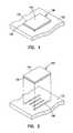
- FIG. 1is a perspective view of a pre-packaged flip chip in accordance with one embodiment, the chip shown attached to a substrate;
- FIG. 2is an exploded perspective view of the flip chip of FIG. 1 ;
- FIG. 3is a partial cut-away perspective view of an active side of a pre-packaged flip chip in accordance with one embodiment (some section lines removed for clarity);
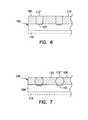
- FIG. 4is section view taken along line 4 - 4 of FIG. 3 illustrating one embodiment (some section lines removed for clarity);
- FIG. 5is another section view taken along line 4 - 4 of FIG. 3 illustrating another embodiment (some section lines removed for clarity);
- FIG. 6is another section view taken along line 4 - 4 of FIG. 3 illustrating yet another embodiment (some section lines removed for clarity);
- FIG. 7is another section view taken along line 4 - 4 of FIG. 3 illustrating still yet another embodiment (some section lines removed for clarity);
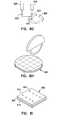
- FIGS. 8A-8Iillustrate wafers at various processing stages according to one embodiment
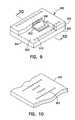
- FIG. 9is a partial cut-away perspective view of a pre-packaged flip chip in accordance with another embodiment (some section lines removed for clarity);
- FIG. 10is a perspective view of a substrate for receiving the pre-packaged flip chip of FIG. 9 ;
- FIG. 11is a section view taken along line 10 - 10 of FIG. 9 illustrating one embodiment of the flip chip of FIG. 9 (some section lines removed for clarity);
- FIG. 12is another section view taken along line 10 - 10 of FIG. 9 illustrating another embodiment of the flip chip of FIG. 9 (some section lines removed for clarity);
- FIGS. 13A-13Killustrate wafers at various processing stages according to another embodiment (some section lines removed for clarity).
- FIG. 14illustrates an electronic system incorporating the pre-packaged flip chip in accordance with one embodiment.
- wafer and substrate used in the following descriptioninclude any base semiconductor structure. Both are to be understood as including silicon-on-sapphire (SOS) technology, silicon-on-insulator (SOI) technology, thin film transistor (TFT) technology, doped and undoped semiconductors, epitaxial layers of a silicon supported by a base semiconductor structure, as well as other semiconductor structures well known to one skilled in the art. Furthermore, when reference is made to a wafer or substrate in the following description, previous process steps may have been utilized to form regions/junctions in the base semiconductor structure, and terms wafer or substrate include the underlying layers containing such regions/junctions. The following detailed description is, therefore, not to be taken in a limiting sense, and the scope of the present invention is defined only by the appended claims and their equivalents.
- the instant inventionis directed to a “pre-packaged” flip chip integrated circuit (IC) device and method for producing the same.
- the pre-packaged IC described hereineliminates the need for underfill operations by forming a flip chip adhesive layer on the package prior to surface mounting.
- the adhesive layeris, in one embodiment, applied at the wafer level. In this way, multiple dice (as many as the wafer provides) can be processed substantially simultaneously. Further, by packaging the die at wafer level, the bare die is handled less often than with conventional packaging operations, thus reducing the opportunity for damage.
- the adhesive layeris applied, it is processed to produce one or more holes or openings therethrough.
- the openingsare produced by exposing and patterning a selected photoresist layer and then chemically etching exposed portions of the adhesive layer to produce the openings.
- other methods of creating the openingsare also contemplated.
- the function of the openingsis to provide access to connection pads on the face of the IC device.
- An electrically conductive materialis then deposited into the openings in accordance with various methods as further discussed below.
- the pre-packaged flip chipis then ready for surface mounting to a receiving component which, for simplicity, will hereinafter be referred to as a support. Examples of a support would include a die attach area of a printed circuit board (PCB) or other device.
- PCBprinted circuit board
- the diemay be packaged at wafer level, allowing greater manufacturing efficiencies including simultaneous packaging of multiple dice.
- the inventionlends itself to multi-chip configurations, permitting packages having even greater mounting densities.
- FIGS. 1-3show an electronic apparatus such as an IC package 100 according to one embodiment of the invention.
- the terms “IC package” and “pre-packaged flip chip”are used throughout the specification to refer to an IC device with its protective package and lead system that allows surface mounting of the device to other electronic components such as a receiving support 102 .
- the IC devicewill hereinafter be described as a semiconductor device such as a chip or die 104 having a first or active side 105 (see FIG. 3 ) and a second or back side 103 .
- the active side 105has an array of electrical connection points or “pads” 107 (see FIG. 3 ) which allow electrical coupling to the electronic circuits 101 on the die 104 .
- the padsare coupled directly to the circuits or, alternatively, coupled to redistribution traces formed in the die 104 which themselves then connect to the circuits.
- the pads 107operatively couple to an array of mating conductors 109 on the support 102 (see FIG. 2 ) via conductive elements 112 (see FIG. 3 ) as further discussed below.
- FIG. 1shows a flip chip adhesive layer 106 between the die 104 and the support 102 .
- the adhesive layerinsulates the conductive elements and prevents damage caused by repeated thermal cycling.
- the adhesive layer 106is partially removed in FIG. 3 to illustrate the pads 107 on the die surface 105 .
- the adhesive layer 106bonds or otherwise adheres to the die surface 105 to form the package 100 .
- FIG. 3One exemplary embodiment of the pre-packaged flip chip 100 is shown in FIG. 3 .
- the die 104is shown with the adhesive layer 106 attached to form the package 100 .
- the adhesive layer 106includes an array of holes or openings 108 which are substantially aligned with the pads 107 (note that while the holes 108 are shown as rectangular, other shapes are equally within the scope of the invention). That is, when the adhesive layer 106 is attached, the pads 107 are accessible through the openings 108 .
- the adhesive layerfurther defines a support mating surface 110 which is adapted to adhere to the support 102 (see FIG. 2 ) as further described below.
- the adhesive layer 106is, in one embodiment, an elastomer applied in fluid form (i.e., applied “wet”) where the fluid is subsequently hardened or cured, or alternatively, in tape-like or film form (i.e., applied “dry”).
- the adhesive layercomprises a thermoplastic material that repeatedly becomes sticky under application of heat. In this case, the transition temperature of the thermoplastic material is selected to ensure the material does not soften during solder reflow or other subsequent processing.
- the adhesive layeris a thermoset material that permanently sets after initial curing.
- the thermoset materialis a “B-stageable” material (i.e., having an intermediate stage in which the material remains wholly or partially plastic and fusible so that it softens when heated).
- the adhesive layeris a pressure-sensitive film that adheres upon contact or under slight application of pressure.
- the material used to form the adhesive layer 106is selected to adequately protect the flip chip package 100 and the support 102 as the two components experience differential expansion during thermal cycling.
- the layeris selected to provide a high modulus, effectively fastening the package 100 to the support 102 and significantly prohibiting relative expansion.
- the layer 106is selected to provide a low modulus to allow the package 102 to expand at a different rate than the support without overstressing either the support 102 or the package 100 .
- the openings 108are formed therein by photo-chemical etching, laser cutting, die cutting, or other techniques.
- the film-type adhesive layer 106is that the openings 108 may be formed, if desired, prior to assembly with the die 104 . By then precisely locating the adhesive layer 106 in registration with the die 104 , the pre-cut openings 108 are properly aligned with the pads 107 on the die surface 105 .
- the openings 108are formed in the adhesive layer 106 after assembly to the die 104 .
- This methodlends itself to use with either the film-type adhesive or the wet adhesive.
- the material used to form the adhesive layer 106is selected so that the openings 108 can be formed using standard photolithographic techniques.
- each opening 108has a conductive material therein which allows electrical connection through the adhesive layer 106 to the pads 107 on the die surface 105 .
- the conductive materialis hereinafter referred to as solder element 112 .
- solder element 112the conductive material
- those skilled in the artwill realize that a variety of conductive materials (e.g., lead-based and lead-free solders, conductive polymers, conductive pastes, etc.) is usable without departing from the scope of the invention.
- the solder elements 112take various forms including cylindrical or column-shaped structures 112 ′ (see FIGS. 4-6 ) and sphere-shaped or ball-like structures 112 ′′ (see FIG. 7 ).
- FIG. 4shows one embodiment of the solder element 112 wherein the element forms a solder column 112 ′ that is slightly recessed from the mating surface 110 .
- the adhesive layer 106includes a chamfer 114 in the vicinity of the opening 108 .
- the chamfer 114 and recessed column 112 ′are particularly advantageous for surface mounting methods which utilize solder paste or flux on the receiving support 102 (see FIG. 2 ).
- any excess paste/fluxis accommodated by the void defined by the chamfer 114 and recessed column 112 ′ rather than spreading across the surface 110 where it can interfere with adhesion of the surface 110 to the support 102 (see FIG. 2 ).
- FIG. 4further illustrates an optional protective coating 116 applied to the back side 103 of the die 104 .
- the coating 116may be an epoxy or other similar material that hardens to protect the back side 103 which would otherwise be exposed after surface mounting as shown in FIG. 1 . Additionally, the coating 116 may a single- or multi-layer material, e.g., an adhesive or adhesive-coated film, that is mounted or laminated to the back side 103 of the die 104 .
- the conductive materialonce again forms a solder column 112 ′.
- the column 112 ′has a generally convex-shaped head 118 that extends beyond or protrudes from the surface 110 .
- the solder column 112 ′is heated sufficiently to become gel-like during surface mounting.
- the heads 118wet the support conductors 109 (see FIG. 2 ) while the surface 110 bonds to the support 102 (see FIG. 2 ).
- the solder columns 112 ′are substantially flush with the surface 110 .
- This particular configurationis advantageous when utilizing a pressure sensitive adhesive layer 106 (i.e., an adhesive layer 106 that comprises a flexible tape which adheres to the support under application of pressure). Because, the solder columns 112 ′ are flush to the surface 110 , the adhesive layer 106 makes consistent, uniform contact with the support 102 (see FIG. 2 ). Once secured to the support 102 , the package is heated to reflow the columns 112 ′ and form the required electrical interconnection.
- solder columns 112 ′are advantageous as the column height can be adjusted to correspond to the desired adhesive layer 106 thickness. Further, the columns are able to deflect and twist to accommodate relative motion between the die 104 and the support 102 .
- solder columns 112 ′While the above-described embodiments utilize solder columns 112 ′, still yet another embodiment utilizes solder balls 112 ′′ as generally shown in FIG. 7 . Like the embodiments described in FIGS. 4-6 , the solder balls 112 ′′ can be recessed within the surface 110 , protrude therefrom, or be relatively flush thereto. The solder balls 112 ′′ are advantageous in that they are cost-efficient to produce and capable of being handled by most semiconductor processing machines. While not shown herein, the solder columns 112 ′ are, in one embodiment, formed by stacked solder balls 112 ′′.
- the methodcomprises applying an adhesive layer to an entire side of a semiconductor wafer (see generally FIG. 8C ) wherein the wafer comprises numerous dice thereon.
- the adhesive layereither includes or is modifiable to include openings having conductive elements therein.
- the adhesive layeradheres to each die on the wafer such that a conductive element is aligned and in contact with each pad on each die.
- the dieis then singulated from the wafer to produce a pre-package flip chip 100 as shown in FIG. 3 and discussed above.
- FIG. 8Ashows a finished wafer 800 (i.e., a wafer that has substantially completed all fabrication processes) having a first or active side or face 802 and a second or back side 804 .
- a finished wafer 800i.e., a wafer that has substantially completed all fabrication processes
- Located on the wafer 800is an array of dice 806 .
- Each die 806has an array of conductive pads 808 as shown in FIG. 8B .
- the pads 808permit electrical connection to circuits on each die 806 .
- FIG. 8Cillustrates an adhesive layer 810 placed over the active side 802 of the wafer 800 .
- the adhesive layer 810comprises an adhesive film 810 ′ that bonds to the wafer 800 .
- the adhesive layer 810comprises a fluid 810 ′′ applied wet via a dispensing apparatus 812 and evenly distributed over the first side 802 .
- the fluid 810 ′′in one embodiment, forms a layer that is hardenable via curing.
- the thickness of the adhesive layer 810is controlled.
- the wafer 800is spun to more evenly distribute the liquid adhesive 810 ′′.
- the wafer 800emerges with a uniform adhesive layer 810 covering the entire active side 802 .
- the latteris, in one embodiment, flipped and a protective coating 814 applied to the back side 804 .
- the protective coating 814comprises a film 814 ′ that bonds to the wafer 800 .
- the protective coating 814comprises a fluid 814 ′′ applied wet via another dispensing apparatus 816 and evenly distributed over the back side 804 (while the apparatus 816 is shown diagrammatically beneath the wafer 800 , it would actually be oriented above the wafer during dispensing).
- the adhesive layer 810is applied, it is—in one embodiment—cured to securely bond it to the wafer 800 . Curing may occur via the application of energy such as heat, light, or radiation (as shown by an energy source 818 in FIG. 8D ).
- the adhesive layer 810is locally removed, as diagrammatically represented in FIG. 8E , from the area of each pad 808 (see FIG. 8B ).
- openings 820are created in the adhesive layer 810 , the openings 820 providing access to the pads 808 on each die 806 as generally shown in FIG. 8F .
- the openings 820are formed by providing a photo-sensitive adhesive layer 810 .
- an energy source 819such as a high intensity ultra-violet light source, as shown in FIG. 8E
- the adhesive layer 810is chemically altered in the area of the openings 820 . The alteration permits the areas to be selectively etched and removed to form the openings 820 .
- Other methods of forming the openings 820are also possible.
- one or more datumsare precisely located on the wafer surface.
- the adhesive layeris chemically or manually removed (in the vicinity of these datums) to expose the datums.
- the masking apparatusthen uses these datums to ensure accurate alignment of the openings 820 with the pads 808 .
- Other methods of aligning the openings 820are also possible within the scope of the invention.
- solder element 822is inserted therein.
- the solder elementcomprises a solder ball 822 ′ as shown in FIG. 8G .
- a solder ball 822 ′is placed into each opening 820 with the use of an apparatus 824 such as a pick-and-place machine (hereinafter PNP).
- PNPpick-and-place machine
- the PNPpicks up the solder ball 822 ′ and precisely places it into each opening 820 .
- multiple balls 822 ′may be stacked in each opening 820 or, alternatively, the PNP is used to place a column of conductive material.
- the apparatus 824is, in another embodiment, a machine similar to the PNP but able to forcefully eject the solder ball 822 ′ into each opening 820 .
- the latter apparatusis advantageous when the solder ball 822 ′ is slightly larger than the opening 820 diameter.
- a paste or gel-like conductive material 822 ′′is placed into each opening 820 to form solder columns such as columns 112 in FIGS. 4-6 .
- the material 822 ′′is dispensed directly into the openings 820 with a dispensing apparatus 826 or, alternatively, applied using stencil/screen techniques (not shown).
- the materialis a combination of underfill, conductive fillers, and flux components that are spin-coated or stenciled over the wafer.
- the conductive fillersmigrate through the liquid adhesive and accumulate at the connection pads via application of electro-magnetic or mechanical energy. This yields a wafer 800 having the required conductive elements without requiring explicit forming of the openings 820 .
- the embodiments described aboveform the openings 820 and locate the solder elements 822 after the adhesive layer 810 is attach to the wafer 800
- another embodiment of the present inventionpre-assembles the adhesive layer 810 and solder elements 822 . That is, the openings 820 are formed and the solder elements 822 are placed in the adhesive layer 810 prior to assembly with the wafer 800 .
- the adhesive layer 810is a film-like adhesive layer 810 ′ similar to that shown in FIG. 8C .
- the openings 820are formed via laser cutting, chemical etching, die cutting or other methods.
- the solder elements 822are then inserted by any of the methods described above.
- the adhesive layer 810 ′ with the pre-assembled solder elements 822is secured to the wafer 800 .
- a removable backing(not shown) may be included with the layer. The removable backing is then removed once the layer 810 ′ is secured.
- another embodiment of the present inventionsecures the solder elements 822 to the wafer prior to application of the adhesive layer.
- a PNPis used to place a solder ball 822 ′ on each connection pad 808 .
- the fluid adhesive 810 ′′is applied.
- the thickness of the adhesive layer 810is controlled relative to the size of the solder balls 822 ′. Accordingly, the order in which the adhesive layer and solder elements are assembled is not perceived to be critical.
- each individual die 806 with the now integral portion of the adhesive layer 810 and the plurality of solder elements 822forms a pre-packaged flip chip 850 as shown in FIG. 8I in accordance with the one embodiment.
- the pre-packaged flip chip 850is then attached to a support 102 such as a motherboard (see FIG. 2 ) where it is, if necessary, reflowed to electrically couple and secure it thereto.
- various embodimentsprovide semiconductor device packages and methods for making semiconductor device packages that are accomplished at wafer level. While the packaged device and method are useful for packaging single chips, it is perceived to be particularly advantageous for accommodating multiple, stacked devices as further described below, allowing even greater chip mounting densities.
- FIG. 9One exemplary embodiment of such a pre-packaged multi-flip chip is shown in FIG. 9 .
- a first semiconductor devicecomprising a die 902 is attached to an active side 903 of a second, larger semiconductor device comprising a die 904 over which a flip chip adhesive layer 906 is applied to produce a pre-packaged, multi-flip chip 900 .
- the multi-flip chip 900like the flip chip 100 illustrated in FIG. 3 , is adapted for mounting to a receiving support 950 having an array of conductors 952 as shown in FIG. 10 .
- the first die 902(see FIG. 9 ) includes a first array of connection pads 908 while the second die 904 includes a second array of connection pads 910 located along the perimeter of the first die 902 .
- the second die 904is sized so that when the first die 902 is secured thereto, the pads 910 are still accessible.
- FIG. 11shows an exemplary embodiment of the package 900 in cross section.
- the first die 902is precisely secured to the second die 904 with a bonding material 912 .
- the adhesive layer 906is then placed over the combined dice 902 , 904 according to any of the methods already described above.
- the adhesive layeris sufficiently thick to ensure that adequate adhesive layer thickness exists over the first die 902 .
- the package 900in one embodiment, includes a protective covering 907 over a back side 905 to protect the package 900 during and after processing.
- the adhesive layer 906is processed to produce an array of openings 914 which are generally aligned with the pads 908 and 910 .
- each opening 914is a solder element 916 .
- the particular shape of the solder elements 916is varied to accommodate the particular application. For instance, in the embodiment illustrated in FIG. 11 , the first array of pads 908 utilize solder balls 916 ′′ while the second array of pads 910 utilize solder columns 916 ′. In FIG. 12 , on the other hand, the first array of pads 908 also utilize a solder column 916 ′.
- the first die 902has one or more pads 908 connected directly to the second die 904 by a wire bond 918 or similar connection. This allows interconnection between the circuits on the dice 902 , 904 within the package 900 .
- the multi-chip, flip chip package 900provides increased circuit densities by stacking multiple dice in a single package.
- the packageoccupies less surface area than singularly packaged die and further permits electrical interconnection of the dice within the package, permitting the use of less complex supports 950 (see FIG. 10 ); i.e., the support needs no conductive trace to interconnect the various conductive pads.
- FIGS. 13A-13KA first wafer 1300 having a first or active side 1302 and a second or back side 1304 is shown in FIG. 13A .
- a bonding material 1310 ′is applied to the back side 1304 with a dispensing apparatus 1308 to produce a bonding layer 1310 (see FIG. 13B ).
- the bonding layer 1310may alternatively be applied in the form of a tape or film (not shown).
- the first wafer 1300is diced as shown in FIG. 13B , producing numerous first dice 1312 as shown in FIG. 13C .
- Each die 1312has an array of connection pads 1314 which permit electrical connection to the circuits on the first die 1312 .
- the first die 1312is then secured to a second wafer 1316 as shown in FIG. 13D .
- the second waferalso has a first or active side 1318 and a second or back side 1320 and numerous, larger second dice 1322 thereon.
- the bonding layer 1310permits the back side 1304 of each first die 1312 to be secured to the active side 1318 of each second die 1322 .
- the bonding layer 1310is a pressure-sensitive material that permits attachment of the dice by application of pressure.
- the bonding layeris a heat-sensitive material (i.e., thermoplastic or thermoset) that bonds to the second die 1322 upon application of heat.
- the pads 1314 of the first die 1312are in close proximity and adjacent to pads 1324 of the second die 1322 .
- the pads 1314 and 1324may be interconnected as shown in FIG. 13E with a wire bond 1326 or similar connection.
- an adhesive material 1328 ′is applied to the active side 1318 of the second wafer 1316 with a dispensing apparatus 1329 forming an adhesive layer 1328 as shown in FIG. 13F .
- Openings 1330are then formed within the adhesive layer 1328 as also shown in FIG. 13F . As with the embodiments already described herein, the openings 1330 are substantially aligned with the pads 1324 and 1314 to allow access thereto.
- the openingsmay be laser cut, chemically etched, or formed in any one of a variety of ways discussed herein with reference to FIGS. 8A-8I .
- solder element 1332is placed therein as shown in FIG. 13G .
- the solder elementis a conductive paste material 1332 ′.
- the solder materialis a solder ball 1332 ′′.
- the resulting wafer 1316as shown in FIG. 13H , has numerous second dice 1322 thereon. Each die 1322 has solder elements 1332 retained within the adhesive layer 1328 formed on the active side 1318 of the second wafer 1316 as shown in FIG. 13I . By then dicing the second wafer 1316 along the scribe lines as shown in FIG. 13J , numerous individual multi-chip flip chip packages 1350 as shown in FIG. 13K are produced.
- various embodimentscan be utilized to package multiple dice at wafer level. By providing multiple dice in one package, higher mounting densities can be achieved. Furthermore, interconnection between multiple dice can be accommodated within the package rather than via the receiving support.
- FIG. 14illustrates the pre-packaged flip chip 100 according to one embodiment shown as part of an electronic system 1400 such as a computer.
- the system 1400includes a processor 1402 and an electronic apparatus such as a pre-packaged flip chip 100 . While diagrammatically depicted as pre-packaged flip chip 100 , other embodiments of the memory component 1404 utilize other flip chips (e.g., flip chip package 850 , 900 , or 1350 ) described herein.
- the flip chip packageis not limited to use with memory components but rather is adapted for use with most any semiconductor device application.
- the packages and methods of the various embodimentsavoid time-consuming underfill operations by prepackaging a die or dice at wafer level.
- the various embodimentsare also particularly amenable to pre-packaging multiple chips in a single module, permitting semiconductor packages having increased electronic densities. Since these multi-chip modules can also be packaged at wafer level, similar manufacturing economies are realized.
Landscapes
- Engineering & Computer Science (AREA)
- Microelectronics & Electronic Packaging (AREA)
- Power Engineering (AREA)
- Computer Hardware Design (AREA)
- Physics & Mathematics (AREA)
- Condensed Matter Physics & Semiconductors (AREA)
- General Physics & Mathematics (AREA)
- Manufacturing & Machinery (AREA)
- Wire Bonding (AREA)
- Dicing (AREA)
Abstract
Description
- This application is a Divisional of U.S. application Ser. No. 10/722,838, filed Nov. 26, 2003, which is a Divisional of U.S. application Ser. No. 09/505,018, filed Feb. 16, 2000, now issued as U.S. Pat. No. 6,710,454, which are incorporated herein by reference.
- This invention relates generally to packaging of semiconductor devices and, more specifically, to an improved flip chip package and method of pre-packaging a flip chip.
- As demand for smaller, more powerful electronic devices grows, semiconductor manufacturers are constantly attempting to reduce the size and cost of not only semiconductor devices themselves but also semiconductor packaging. Smaller packages equate with higher semiconductor mounting densities and higher mounting densities allow for more compact and yet more capable devices.
- With conventional packaging methods, a semiconductor die or “chip” is singulated from the silicon wafer and is encapsulated in a ceramic or plastic package having a number of electrical leads extending therefrom. The leads permit electrical connection between external components and the circuits on the die. Although these packages have proven reliable, they are generally many times larger than the actual die. In addition, the configuration of these packages typically yields only a limited number of leads. For these reasons, conventional packaging techniques are not particularly adaptable to high density packaging.
- Accordingly, more efficient chip packages have been developed. One such package is the “pin grid array” or PGA which utilizes a series of pin conductors extending from the face of the package. While PGAs provide increased electrical interconnection density, the pins forming the PGA are fragile and easily bent. In addition, the PGA is relatively expensive to produce and of limited value when the package is to be permanently mounted.
- Similar to the PGA are various flip chip packages including the “ball grid array” or BGA. Instead of pins, the BGA has an array of solder bumps or balls attached to the active face of the package in a process called “bumping.” The array of solder bumps is adapted to mate with discreet contacts on a receiving component. The package may be subsequently heated to partially liquefy or “reflow” the bumps, thus forming electrical connections at the discreet locations. This technology is frequently referred to as “flip chip” because the solder balls are typically secured to the semiconductor package wherein the package is then “flipped” to secure it to the receiving component. The present invention is directed primarily to flip chip packaging technology and the remainder of this discussion will focus on the same.
- While flip chip processes have proven effective, problems remain. For instance, conventional flip chip technology requires an underfill layer between the semiconductor package and the receiving substrate. The underfill material reduces stress on the solder bumps caused by thermal mismatch between the semiconductor package and substrate. The underfill layer further provides insulation between the device and substrate and prevents creep flow at the solder interface. Without the underfill layer, repeated thermal cycling constantly stresses the solder interconnections, potentially leading to failure.
- Unfortunately, the underfill process is time consuming and expensive. For example, the equipment used to dispense the underfill must precisely maintain the viscosity of the material, dispensing it at a particular flow rate and within a predetermined temperature range. Further, the underfill process cannot be applied until the package is secured to its receiving substrate. Accordingly, the chip package and substrate design must permit the dispensing equipment direct access to the package/substrate interface. And still further, since the underfill material is distributed via capillary action, the time required to complete the underfill operation can be significant.
- One method which avoids the use of underfill material involves the use of a resilient retaining member which supports a series of solder preforms therein. The retaining member is sandwiched between conductive elements such that the preforms effect electrical connection therebetween. Like underfill, however, the retaining member/solder preform is only utilized during actual surface mounting of individual chips.
- While underfill processes as well as retaining member/preforms are more than adequate in many applications, current trends in IC fabrication favor completing more and more process steps—many of which would not normally occur until after die singulation—at the wafer level. Wafer level processing is advantageous over conventional methods as it allows multiple ICs (equal to the number of die on the wafer face) to be processed simultaneously rather than serially as typically required after die singulation. Accordingly, the time required to produce a given IC device can be dramatically reduced.
- While some processes lend themselves to wafer level processing, known packaging methods such as underfill and retaining member/preform methods unfortunately do not. Thus, what is needed is a flip chip package that can be assembled at wafer level. What is further needed is a package that avoids the problems with underfill materials including troublesome dispensing and assembly cycle times. The present invention is directed to a package and method that addresses these issues.
FIG. 1 is a perspective view of a pre-packaged flip chip in accordance with one embodiment, the chip shown attached to a substrate;FIG. 2 is an exploded perspective view of the flip chip ofFIG. 1 ;FIG. 3 is a partial cut-away perspective view of an active side of a pre-packaged flip chip in accordance with one embodiment (some section lines removed for clarity);FIG. 4 is section view taken along line4-4 ofFIG. 3 illustrating one embodiment (some section lines removed for clarity);FIG. 5 is another section view taken along line4-4 ofFIG. 3 illustrating another embodiment (some section lines removed for clarity);FIG. 6 is another section view taken along line4-4 ofFIG. 3 illustrating yet another embodiment (some section lines removed for clarity);FIG. 7 is another section view taken along line4-4 ofFIG. 3 illustrating still yet another embodiment (some section lines removed for clarity);FIGS. 8A-8I illustrate wafers at various processing stages according to one embodiment;FIG. 9 is a partial cut-away perspective view of a pre-packaged flip chip in accordance with another embodiment (some section lines removed for clarity);FIG. 10 is a perspective view of a substrate for receiving the pre-packaged flip chip ofFIG. 9 ;FIG. 11 is a section view taken along line10-10 ofFIG. 9 illustrating one embodiment of the flip chip ofFIG. 9 (some section lines removed for clarity);FIG. 12 is another section view taken along line10-10 ofFIG. 9 illustrating another embodiment of the flip chip ofFIG. 9 (some section lines removed for clarity);FIGS. 13A-13K illustrate wafers at various processing stages according to another embodiment (some section lines removed for clarity); andFIG. 14 illustrates an electronic system incorporating the pre-packaged flip chip in accordance with one embodiment.- In the following detailed description of the preferred embodiments, reference is made to the accompanying drawings which form a part hereof, and in which is shown by way of illustration specific embodiments in which the inventions may be practiced. These embodiments are described in sufficient detail to enable those skilled in the art to practice the invention, and it is to be understood that other embodiments may be utilized and that process, electrical or mechanical changes may be made without departing from the scope of the present invention.
- The terms wafer and substrate used in the following description include any base semiconductor structure. Both are to be understood as including silicon-on-sapphire (SOS) technology, silicon-on-insulator (SOI) technology, thin film transistor (TFT) technology, doped and undoped semiconductors, epitaxial layers of a silicon supported by a base semiconductor structure, as well as other semiconductor structures well known to one skilled in the art. Furthermore, when reference is made to a wafer or substrate in the following description, previous process steps may have been utilized to form regions/junctions in the base semiconductor structure, and terms wafer or substrate include the underlying layers containing such regions/junctions. The following detailed description is, therefore, not to be taken in a limiting sense, and the scope of the present invention is defined only by the appended claims and their equivalents.
- Broadly speaking, the instant invention is directed to a “pre-packaged” flip chip integrated circuit (IC) device and method for producing the same. Unlike conventional flip chip packages, the pre-packaged IC described herein eliminates the need for underfill operations by forming a flip chip adhesive layer on the package prior to surface mounting. To maximize throughput, the adhesive layer is, in one embodiment, applied at the wafer level. In this way, multiple dice (as many as the wafer provides) can be processed substantially simultaneously. Further, by packaging the die at wafer level, the bare die is handled less often than with conventional packaging operations, thus reducing the opportunity for damage.
- Once the adhesive layer is applied, it is processed to produce one or more holes or openings therethrough. In one embodiment, the openings are produced by exposing and patterning a selected photoresist layer and then chemically etching exposed portions of the adhesive layer to produce the openings. However, other methods of creating the openings are also contemplated.
- The function of the openings is to provide access to connection pads on the face of the IC device. An electrically conductive material is then deposited into the openings in accordance with various methods as further discussed below. The pre-packaged flip chip is then ready for surface mounting to a receiving component which, for simplicity, will hereinafter be referred to as a support. Examples of a support would include a die attach area of a printed circuit board (PCB) or other device. The electrically conductive material is then re-flowed to interconnect the circuits on the IC to conductors on the support.
- By prepackaging the flip chip, messy, expensive, and time-consuming underfill operations are avoided. In addition, by utilizing various embodiments of the invention, the die may be packaged at wafer level, allowing greater manufacturing efficiencies including simultaneous packaging of multiple dice. Furthermore, as described below, the invention lends itself to multi-chip configurations, permitting packages having even greater mounting densities.
- With this brief introduction, specific embodiments of the instant invention will now be described. Although the description focuses on particular embodiments, the reader is reminded that such embodiments are exemplary only and are therefore intended merely to teach one of skill in the art how to make and use the invention. Other embodiments are certainly possible without departing from the scope of the invention.
FIGS. 1-3 show an electronic apparatus such as anIC package 100 according to one embodiment of the invention. The terms “IC package” and “pre-packaged flip chip” are used throughout the specification to refer to an IC device with its protective package and lead system that allows surface mounting of the device to other electronic components such as a receivingsupport 102. In the context of chip scale devices (CSD), the IC device will hereinafter be described as a semiconductor device such as a chip or die104 having a first or active side105 (seeFIG. 3 ) and a second or backside 103. Theactive side 105 has an array of electrical connection points or “pads”107 (seeFIG. 3 ) which allow electrical coupling to theelectronic circuits 101 on thedie 104. The pads are coupled directly to the circuits or, alternatively, coupled to redistribution traces formed in thedie 104 which themselves then connect to the circuits. Thepads 107 operatively couple to an array ofmating conductors 109 on the support102 (seeFIG. 2 ) via conductive elements112 (seeFIG. 3 ) as further discussed below.FIG. 1 shows a flip chipadhesive layer 106 between the die104 and thesupport 102. The adhesive layer insulates the conductive elements and prevents damage caused by repeated thermal cycling. For clarity, theadhesive layer 106 is partially removed inFIG. 3 to illustrate thepads 107 on thedie surface 105. Theadhesive layer 106 bonds or otherwise adheres to thedie surface 105 to form thepackage 100.- One exemplary embodiment of the
pre-packaged flip chip 100 is shown inFIG. 3 . Here thedie 104 is shown with theadhesive layer 106 attached to form thepackage 100. To provide electrical interconnection to thepads 107 on the die, theadhesive layer 106 includes an array of holes oropenings 108 which are substantially aligned with the pads107 (note that while theholes 108 are shown as rectangular, other shapes are equally within the scope of the invention). That is, when theadhesive layer 106 is attached, thepads 107 are accessible through theopenings 108. The adhesive layer further defines asupport mating surface 110 which is adapted to adhere to the support102 (seeFIG. 2 ) as further described below. - The
adhesive layer 106 is, in one embodiment, an elastomer applied in fluid form (i.e., applied “wet”) where the fluid is subsequently hardened or cured, or alternatively, in tape-like or film form (i.e., applied “dry”). In one embodiment, the adhesive layer comprises a thermoplastic material that repeatedly becomes sticky under application of heat. In this case, the transition temperature of the thermoplastic material is selected to ensure the material does not soften during solder reflow or other subsequent processing. In another embodiment, the adhesive layer is a thermoset material that permanently sets after initial curing. Alternatively, the thermoset material is a “B-stageable” material (i.e., having an intermediate stage in which the material remains wholly or partially plastic and fusible so that it softens when heated). - In still yet another embodiment, the adhesive layer is a pressure-sensitive film that adheres upon contact or under slight application of pressure.
- The material used to form the
adhesive layer 106 is selected to adequately protect theflip chip package 100 and thesupport 102 as the two components experience differential expansion during thermal cycling. In one embodiment, the layer is selected to provide a high modulus, effectively fastening thepackage 100 to thesupport 102 and significantly prohibiting relative expansion. In another embodiment, thelayer 106 is selected to provide a low modulus to allow thepackage 102 to expand at a different rate than the support without overstressing either thesupport 102 or thepackage 100. - To form the
openings 108, various methods are used. For example, where theadhesive layer 106 comprises a film, theopenings 108 are formed therein by photo-chemical etching, laser cutting, die cutting, or other techniques. One advantage to the film-type adhesive layer 106 is that theopenings 108 may be formed, if desired, prior to assembly with thedie 104. By then precisely locating theadhesive layer 106 in registration with thedie 104, thepre-cut openings 108 are properly aligned with thepads 107 on thedie surface 105. - Alternatively, the
openings 108 are formed in theadhesive layer 106 after assembly to thedie 104. This method lends itself to use with either the film-type adhesive or the wet adhesive. With post-formation of theopenings 108, the material used to form theadhesive layer 106 is selected so that theopenings 108 can be formed using standard photolithographic techniques. - Still referring to
FIG. 3 , eachopening 108 has a conductive material therein which allows electrical connection through theadhesive layer 106 to thepads 107 on thedie surface 105. For simplicity, the conductive material is hereinafter referred to assolder element 112. However, those skilled in the art will realize that a variety of conductive materials (e.g., lead-based and lead-free solders, conductive polymers, conductive pastes, etc.) is usable without departing from the scope of the invention. - The
solder elements 112, as described below, take various forms including cylindrical or column-shapedstructures 112′ (seeFIGS. 4-6 ) and sphere-shaped or ball-like structures 112″ (seeFIG. 7 ).FIG. 4 shows one embodiment of thesolder element 112 wherein the element forms asolder column 112′ that is slightly recessed from themating surface 110. In this particular embodiment, theadhesive layer 106 includes a chamfer114 in the vicinity of theopening 108. The chamfer114 and recessedcolumn 112′ are particularly advantageous for surface mounting methods which utilize solder paste or flux on the receiving support102 (seeFIG. 2 ). When thepackage 100 is surface mounted, any excess paste/flux is accommodated by the void defined by the chamfer114 and recessedcolumn 112′ rather than spreading across thesurface 110 where it can interfere with adhesion of thesurface 110 to the support102 (seeFIG. 2 ). FIG. 4 further illustrates an optionalprotective coating 116 applied to theback side 103 of thedie 104. Thecoating 116 may be an epoxy or other similar material that hardens to protect theback side 103 which would otherwise be exposed after surface mounting as shown inFIG. 1 . Additionally, thecoating 116 may a single- or multi-layer material, e.g., an adhesive or adhesive-coated film, that is mounted or laminated to theback side 103 of thedie 104.- Other embodiments are also possible. For example, in
FIG. 5 , the conductive material once again forms asolder column 112′. However, in this particular embodiment, thecolumn 112′ has a generally convex-shaped head118 that extends beyond or protrudes from thesurface 110. Thesolder column 112′ is heated sufficiently to become gel-like during surface mounting. When the package is brought into registration with the support102 (seeFIG. 2 ), the heads118 wet the support conductors109 (seeFIG. 2 ) while thesurface 110 bonds to the support102 (seeFIG. 2 ). - In still another embodiment such as that shown in
FIG. 6 , thesolder columns 112′ are substantially flush with thesurface 110. This particular configuration is advantageous when utilizing a pressure sensitive adhesive layer106 (i.e., anadhesive layer 106 that comprises a flexible tape which adheres to the support under application of pressure). Because, thesolder columns 112′ are flush to thesurface 110, theadhesive layer 106 makes consistent, uniform contact with the support102 (see FIG.2). Once secured to thesupport 102, the package is heated to reflow thecolumns 112′ and form the required electrical interconnection. - The
solder columns 112′ are advantageous as the column height can be adjusted to correspond to the desiredadhesive layer 106 thickness. Further, the columns are able to deflect and twist to accommodate relative motion between the die104 and thesupport 102. - While the above-described embodiments utilize
solder columns 112′, still yet another embodiment utilizessolder balls 112″ as generally shown inFIG. 7 . Like the embodiments described inFIGS. 4-6 , thesolder balls 112″ can be recessed within thesurface 110, protrude therefrom, or be relatively flush thereto. Thesolder balls 112″ are advantageous in that they are cost-efficient to produce and capable of being handled by most semiconductor processing machines. While not shown herein, thesolder columns 112′ are, in one embodiment, formed by stackedsolder balls 112″. - Having described various exemplary embodiments of the
pre-packaged flip chip 100, a method for producing the package will now be described in accordance with one exemplary embodiment. In describing the method, only those processes necessary for one of ordinary skill in the art to understand the invention are described in detail. Other fabrication processes that are well known or are unnecessary for a complete understanding of the invention are excluded. - As mentioned above, various embodiments of the invention are perceived to be particularly advantageous for pre-packaging dice at wafer level. Generally speaking, the method, according to one embodiment, comprises applying an adhesive layer to an entire side of a semiconductor wafer (see generally
FIG. 8C ) wherein the wafer comprises numerous dice thereon. As described above, the adhesive layer either includes or is modifiable to include openings having conductive elements therein. The adhesive layer adheres to each die on the wafer such that a conductive element is aligned and in contact with each pad on each die. The die is then singulated from the wafer to produce apre-package flip chip 100 as shown inFIG. 3 and discussed above. - With this general introduction, an exemplary method of making the pre-packaged flip chip in accordance is now described with reference to
FIGS. 8A-8I .FIG. 8A shows a finished wafer800 (i.e., a wafer that has substantially completed all fabrication processes) having a first or active side orface 802 and a second or backside 804. Located on thewafer 800 is an array ofdice 806. Each die806 has an array ofconductive pads 808 as shown inFIG. 8B . Thepads 808 permit electrical connection to circuits on each die806. FIG. 8C illustrates anadhesive layer 810 placed over theactive side 802 of thewafer 800. In one embodiment, theadhesive layer 810 comprises anadhesive film 810′ that bonds to thewafer 800. In another embodiment, theadhesive layer 810 comprises a fluid810″ applied wet via adispensing apparatus 812 and evenly distributed over thefirst side 802. The fluid810″, in one embodiment, forms a layer that is hardenable via curing. By controlling the viscosity and volume of theadhesive liquid 810″ dispensed, the thickness of theadhesive layer 810 is controlled. In one embodiment, thewafer 800 is spun to more evenly distribute theliquid adhesive 810″. Thewafer 800 emerges with a uniformadhesive layer 810 covering the entireactive side 802.- To protect the
back side 804 of thewafer 800, the latter is, in one embodiment, flipped and aprotective coating 814 applied to theback side 804. In one embodiment, theprotective coating 814 comprises afilm 814′ that bonds to thewafer 800. In another embodiment, theprotective coating 814 comprises a fluid814″ applied wet via anotherdispensing apparatus 816 and evenly distributed over the back side804 (while theapparatus 816 is shown diagrammatically beneath thewafer 800, it would actually be oriented above the wafer during dispensing). - Once the
adhesive layer 810 is applied, it is—in one embodiment—cured to securely bond it to thewafer 800. Curing may occur via the application of energy such as heat, light, or radiation (as shown by anenergy source 818 inFIG. 8D ). - Once cured, the
adhesive layer 810 is locally removed, as diagrammatically represented inFIG. 8E , from the area of each pad808 (seeFIG. 8B ). In other words,openings 820 are created in theadhesive layer 810, theopenings 820 providing access to thepads 808 on each die806 as generally shown inFIG. 8F . In one embodiment, theopenings 820 are formed by providing a photo-sensitive adhesive layer 810. By masking the appropriate areas of theadhesive layer 810 and exposing the latter to anenergy source 819, such as a high intensity ultra-violet light source, as shown inFIG. 8E , theadhesive layer 810 is chemically altered in the area of theopenings 820. The alteration permits the areas to be selectively etched and removed to form theopenings 820. Other methods of forming theopenings 820 are also possible. - To accurately locate the openings, one or more datums (not shown) are precisely located on the wafer surface. The adhesive layer is chemically or manually removed (in the vicinity of these datums) to expose the datums. The masking apparatus then uses these datums to ensure accurate alignment of the
openings 820 with thepads 808. Other methods of aligning theopenings 820 are also possible within the scope of the invention. - Once the
openings 820 are formed, asolder element 822 is inserted therein. In one embodiment, the solder element comprises asolder ball 822′ as shown inFIG. 8G . Asolder ball 822′ is placed into each opening820 with the use of anapparatus 824 such as a pick-and-place machine (hereinafter PNP). The PNP picks up thesolder ball 822′ and precisely places it into eachopening 820. To form a solder column,multiple balls 822′ may be stacked in eachopening 820 or, alternatively, the PNP is used to place a column of conductive material. Theapparatus 824 is, in another embodiment, a machine similar to the PNP but able to forcefully eject thesolder ball 822′ into eachopening 820. The latter apparatus is advantageous when thesolder ball 822′ is slightly larger than theopening 820 diameter. - In still yet another embodiment, a paste or gel-like
conductive material 822″ is placed into each opening820 to form solder columns such ascolumns 112 inFIGS. 4-6 . Thematerial 822″ is dispensed directly into theopenings 820 with adispensing apparatus 826 or, alternatively, applied using stencil/screen techniques (not shown). - Still other embodiments are possible for securing the adhesive layer and forming the conductive element. For instance, in the case of a wet adhesive layer, the material is a combination of underfill, conductive fillers, and flux components that are spin-coated or stenciled over the wafer. The conductive fillers migrate through the liquid adhesive and accumulate at the connection pads via application of electro-magnetic or mechanical energy. This yields a
wafer 800 having the required conductive elements without requiring explicit forming of theopenings 820. - While the embodiments described above form the
openings 820 and locate thesolder elements 822 after theadhesive layer 810 is attach to thewafer 800, another embodiment of the present invention pre-assembles theadhesive layer 810 andsolder elements 822. That is, theopenings 820 are formed and thesolder elements 822 are placed in theadhesive layer 810 prior to assembly with thewafer 800. For example, in one embodiment, theadhesive layer 810 is a film-likeadhesive layer 810′ similar to that shown inFIG. 8C . Theopenings 820 are formed via laser cutting, chemical etching, die cutting or other methods. Thesolder elements 822 are then inserted by any of the methods described above. At this point, theadhesive layer 810′ with thepre-assembled solder elements 822 is secured to thewafer 800. To minimize deformation prior to applying theadhesive layer 810′, a removable backing (not shown) may be included with the layer. The removable backing is then removed once thelayer 810′ is secured. - While not shown in the figures, another embodiment of the present invention secures the
solder elements 822 to the wafer prior to application of the adhesive layer. For example, a PNP is used to place asolder ball 822′ on eachconnection pad 808. After placing thesolder balls 822, thefluid adhesive 810″ is applied. By controlling the volume of the adhesive applied, the thickness of theadhesive layer 810 is controlled relative to the size of thesolder balls 822′. Accordingly, the order in which the adhesive layer and solder elements are assembled is not perceived to be critical. - Once the
solder elements 822 are positioned and retained within theadhesive layer 810 and the adhesive layer is secured to thewafer 800, the wafer is singulated intoindividual dice 806 by sawing as shown inFIG. 8H . Once singulated, eachindividual die 806 with the now integral portion of theadhesive layer 810 and the plurality ofsolder elements 822 forms apre-packaged flip chip 850 as shown inFIG. 8I in accordance with the one embodiment. Thepre-packaged flip chip 850 is then attached to asupport 102 such as a motherboard (seeFIG. 2 ) where it is, if necessary, reflowed to electrically couple and secure it thereto. - Accordingly, various embodiments provide semiconductor device packages and methods for making semiconductor device packages that are accomplished at wafer level. While the packaged device and method are useful for packaging single chips, it is perceived to be particularly advantageous for accommodating multiple, stacked devices as further described below, allowing even greater chip mounting densities.
- One exemplary embodiment of such a pre-packaged multi-flip chip is shown in
FIG. 9 . Here, a first semiconductor device comprising adie 902 is attached to anactive side 903 of a second, larger semiconductor device comprising adie 904 over which a flip chipadhesive layer 906 is applied to produce a pre-packaged,multi-flip chip 900. Themulti-flip chip 900, like theflip chip 100 illustrated inFIG. 3 , is adapted for mounting to a receivingsupport 950 having an array ofconductors 952 as shown inFIG. 10 . - The first die902 (see
FIG. 9 ) includes a first array ofconnection pads 908 while thesecond die 904 includes a second array ofconnection pads 910 located along the perimeter of thefirst die 902. Thesecond die 904 is sized so that when thefirst die 902 is secured thereto, thepads 910 are still accessible. FIG. 11 shows an exemplary embodiment of thepackage 900 in cross section. Thefirst die 902 is precisely secured to thesecond die 904 with abonding material 912. Theadhesive layer 906 is then placed over the combineddice first die 902. Like the embodiments described above, thepackage 900, in one embodiment, includes aprotective covering 907 over aback side 905 to protect thepackage 900 during and after processing.- As with the embodiments already described herein, the
adhesive layer 906 is processed to produce an array ofopenings 914 which are generally aligned with thepads opening 914 is asolder element 916. The particular shape of thesolder elements 916 is varied to accommodate the particular application. For instance, in the embodiment illustrated inFIG. 11 , the first array ofpads 908 utilizesolder balls 916″ while the second array ofpads 910 utilizesolder columns 916′. InFIG. 12 , on the other hand, the first array ofpads 908 also utilize asolder column 916′. In this particular embodiment, thefirst die 902 has one ormore pads 908 connected directly to thesecond die 904 by awire bond 918 or similar connection. This allows interconnection between the circuits on thedice package 900. - The multi-chip,
flip chip package 900 provides increased circuit densities by stacking multiple dice in a single package. Thus, the package occupies less surface area than singularly packaged die and further permits electrical interconnection of the dice within the package, permitting the use of less complex supports950 (seeFIG. 10 ); i.e., the support needs no conductive trace to interconnect the various conductive pads. - Having described a multi-chip flip chip package according to one embodiment, an exemplary method of making the multi-chip package will now be described with reference to
FIGS. 13A-13K . Afirst wafer 1300 having a first oractive side 1302 and a second or backside 1304 is shown inFIG. 13A . Abonding material 1310′ is applied to theback side 1304 with adispensing apparatus 1308 to produce a bonding layer1310 (seeFIG. 13B ). Thebonding layer 1310 may alternatively be applied in the form of a tape or film (not shown). Once thebonding layer 1310 is formed, thefirst wafer 1300 is diced as shown inFIG. 13B , producing numerousfirst dice 1312 as shown inFIG. 13C . Each die1312 has an array ofconnection pads 1314 which permit electrical connection to the circuits on thefirst die 1312. - The
first die 1312 is then secured to asecond wafer 1316 as shown inFIG. 13D . The second wafer also has a first oractive side 1318 and a second or backside 1320 and numerous, largersecond dice 1322 thereon. Thebonding layer 1310 permits theback side 1304 of eachfirst die 1312 to be secured to theactive side 1318 of eachsecond die 1322. In one embodiment, thebonding layer 1310 is a pressure-sensitive material that permits attachment of the dice by application of pressure. In an alternative embodiment, the bonding layer is a heat-sensitive material (i.e., thermoplastic or thermoset) that bonds to thesecond die 1322 upon application of heat. - After securing the
first die 1312 to thesecond die 1322, thepads 1314 of thefirst die 1312 are in close proximity and adjacent topads 1324 of thesecond die 1322. As such, thepads FIG. 13E with awire bond 1326 or similar connection. After interconnection, anadhesive material 1328′ is applied to theactive side 1318 of thesecond wafer 1316 with adispensing apparatus 1329 forming anadhesive layer 1328 as shown inFIG. 13F . Openings 1330 are then formed within theadhesive layer 1328 as also shown inFIG. 13F . As with the embodiments already described herein, theopenings 1330 are substantially aligned with thepads FIGS. 8A-8I .- Once the
openings 1330 are formed, asolder element 1332 is placed therein as shown inFIG. 13G . In one embodiment, the solder element is aconductive paste material 1332′. In another embodiment, the solder material is asolder ball 1332″. The resultingwafer 1316, as shown inFIG. 13H , has numeroussecond dice 1322 thereon. Each die1322 hassolder elements 1332 retained within theadhesive layer 1328 formed on theactive side 1318 of thesecond wafer 1316 as shown inFIG. 13I . By then dicing thesecond wafer 1316 along the scribe lines as shown inFIG. 13J , numerous individual multi-chipflip chip packages 1350 as shown inFIG. 13K are produced. - Thus, various embodiments can be utilized to package multiple dice at wafer level. By providing multiple dice in one package, higher mounting densities can be achieved. Furthermore, interconnection between multiple dice can be accommodated within the package rather than via the receiving support.
FIG. 14 illustrates thepre-packaged flip chip 100 according to one embodiment shown as part of anelectronic system 1400 such as a computer. Thesystem 1400, in one embodiment, includes aprocessor 1402 and an electronic apparatus such as apre-packaged flip chip 100. While diagrammatically depicted aspre-packaged flip chip 100, other embodiments of thememory component 1404 utilize other flip chips (e.g.,flip chip package - Advantageously, the packages and methods of the various embodiments avoid time-consuming underfill operations by prepackaging a die or dice at wafer level. By packaging the die at wafer level, greater manufacturing efficiencies are obtainable due to simultaneous processing of multiple dice across the entire wafer face. In addition, the various embodiments are also particularly amenable to pre-packaging multiple chips in a single module, permitting semiconductor packages having increased electronic densities. Since these multi-chip modules can also be packaged at wafer level, similar manufacturing economies are realized.
- Preferred embodiments of the present invention are described above. Those skilled in the art will recognize that many embodiments are possible within the scope of the invention. Variations, modifications, and combinations of the various parts and assemblies can certainly be made and still fall within the scope of the invention. Thus, the invention is limited only by the following claims, and equivalents thereto.
Claims (57)
Priority Applications (1)
| Application Number | Priority Date | Filing Date | Title |
|---|---|---|---|
| US11/460,089US7943422B2 (en) | 2000-02-16 | 2006-07-26 | Wafer level pre-packaged flip chip |
Applications Claiming Priority (3)
| Application Number | Priority Date | Filing Date | Title |
|---|---|---|---|
| US09/505,018US6710454B1 (en) | 2000-02-16 | 2000-02-16 | Adhesive layer for an electronic apparatus having multiple semiconductor devices |
| US10/722,838US20040113246A1 (en) | 2000-02-16 | 2003-11-26 | Method of packaging at a wafer level |
| US11/460,089US7943422B2 (en) | 2000-02-16 | 2006-07-26 | Wafer level pre-packaged flip chip |
Related Parent Applications (1)
| Application Number | Title | Priority Date | Filing Date |
|---|---|---|---|
| US10/722,838DivisionUS20040113246A1 (en) | 2000-02-16 | 2003-11-26 | Method of packaging at a wafer level |
Publications (2)
| Publication Number | Publication Date |
|---|---|
| US20060258052A1true US20060258052A1 (en) | 2006-11-16 |
| US7943422B2 US7943422B2 (en) | 2011-05-17 |
Family
ID=31978900
Family Applications (7)
| Application Number | Title | Priority Date | Filing Date |
|---|---|---|---|
| US09/505,018Expired - LifetimeUS6710454B1 (en) | 2000-02-16 | 2000-02-16 | Adhesive layer for an electronic apparatus having multiple semiconductor devices |
| US10/722,838AbandonedUS20040113246A1 (en) | 2000-02-16 | 2003-11-26 | Method of packaging at a wafer level |
| US10/723,474AbandonedUS20040104486A1 (en) | 2000-02-16 | 2003-11-26 | Electronic apparatus having an adhesive layer from wafer level packaging |
| US11/460,093Expired - Fee RelatedUS7812447B2 (en) | 2000-02-16 | 2006-07-26 | Wafer level pre-packaged flip chip |
| US11/460,089Expired - Fee RelatedUS7943422B2 (en) | 2000-02-16 | 2006-07-26 | Wafer level pre-packaged flip chip |
| US11/460,445Expired - Fee RelatedUS7808112B2 (en) | 2000-02-16 | 2006-07-27 | Wafer level pre-packaged flip chip system |
| US11/460,435Expired - Fee RelatedUS7646102B2 (en) | 2000-02-16 | 2006-07-27 | Wafer level pre-packaged flip chip systems |
Family Applications Before (4)
| Application Number | Title | Priority Date | Filing Date |
|---|---|---|---|
| US09/505,018Expired - LifetimeUS6710454B1 (en) | 2000-02-16 | 2000-02-16 | Adhesive layer for an electronic apparatus having multiple semiconductor devices |
| US10/722,838AbandonedUS20040113246A1 (en) | 2000-02-16 | 2003-11-26 | Method of packaging at a wafer level |
| US10/723,474AbandonedUS20040104486A1 (en) | 2000-02-16 | 2003-11-26 | Electronic apparatus having an adhesive layer from wafer level packaging |
| US11/460,093Expired - Fee RelatedUS7812447B2 (en) | 2000-02-16 | 2006-07-26 | Wafer level pre-packaged flip chip |
Family Applications After (2)
| Application Number | Title | Priority Date | Filing Date |
|---|---|---|---|
| US11/460,445Expired - Fee RelatedUS7808112B2 (en) | 2000-02-16 | 2006-07-27 | Wafer level pre-packaged flip chip system |
| US11/460,435Expired - Fee RelatedUS7646102B2 (en) | 2000-02-16 | 2006-07-27 | Wafer level pre-packaged flip chip systems |
Country Status (1)
| Country | Link |
|---|---|
| US (7) | US6710454B1 (en) |
Cited By (2)
| Publication number | Priority date | Publication date | Assignee | Title |
|---|---|---|---|---|
| US20040104486A1 (en)* | 2000-02-16 | 2004-06-03 | Micron Technology, Inc. | Electronic apparatus having an adhesive layer from wafer level packaging |
| US20090184412A1 (en)* | 2007-10-25 | 2009-07-23 | Rohm Co., Ltd. | Resin-seal type semiconductor device |
Families Citing this family (113)
| Publication number | Priority date | Publication date | Assignee | Title |
|---|---|---|---|---|
| US6642613B1 (en)* | 2000-05-09 | 2003-11-04 | National Semiconductor Corporation | Techniques for joining an opto-electronic module to a semiconductor package |
| US6875640B1 (en) | 2000-06-08 | 2005-04-05 | Micron Technology, Inc. | Stereolithographic methods for forming a protective layer on a semiconductor device substrate and substrates including protective layers so formed |
| DE10046296C2 (en)* | 2000-07-17 | 2002-10-10 | Infineon Technologies Ag | Electronic chip component with an integrated circuit and method for its production |
| US7498196B2 (en)* | 2001-03-30 | 2009-03-03 | Megica Corporation | Structure and manufacturing method of chip scale package |
| TW584950B (en) | 2001-12-31 | 2004-04-21 | Megic Corp | Chip packaging structure and process thereof |
| US6673698B1 (en) | 2002-01-19 | 2004-01-06 | Megic Corporation | Thin film semiconductor package utilizing a glass substrate with composite polymer/metal interconnect layers |
| TW544882B (en)* | 2001-12-31 | 2003-08-01 | Megic Corp | Chip package structure and process thereof |
| TW503496B (en) | 2001-12-31 | 2002-09-21 | Megic Corp | Chip packaging structure and manufacturing process of the same |
| US7579681B2 (en)* | 2002-06-11 | 2009-08-25 | Micron Technology, Inc. | Super high density module with integrated wafer level packages |
| SG111069A1 (en)* | 2002-06-18 | 2005-05-30 | Micron Technology Inc | Semiconductor devices including peripherally located bond pads, assemblies, packages, and methods |
| SG107595A1 (en) | 2002-06-18 | 2004-12-29 | Micron Technology Inc | Semiconductor devices and semiconductor device components with peripherally located, castellated contacts, assembles and packages including such semiconductor devices or packages and associated methods |
| US6936929B1 (en)* | 2003-03-17 | 2005-08-30 | National Semiconductor Corporation | Multichip packages with exposed dice |
| KR20050001159A (en)* | 2003-06-27 | 2005-01-06 | 삼성전자주식회사 | Multi-chip package having a plurality of flip chips and fabrication method thereof |
| SG120123A1 (en) | 2003-09-30 | 2006-03-28 | Micron Technology Inc | Castellated chip-scale packages and methods for fabricating the same |
| US20050072121A1 (en)* | 2003-10-06 | 2005-04-07 | Texas Instruments Incorporated | Method and system for shipping semiconductor wafers |
| US20070102831A1 (en)* | 2003-12-24 | 2007-05-10 | Shuntaro Machida | Device and method of manufacturing the same |
| US7122906B2 (en)* | 2004-01-29 | 2006-10-17 | Micron Technology, Inc. | Die-wafer package and method of fabricating same |
| US6987314B1 (en) | 2004-06-08 | 2006-01-17 | Amkor Technology, Inc. | Stackable semiconductor package with solder on pads on which second semiconductor package is stacked |
| KR101313391B1 (en) | 2004-11-03 | 2013-10-01 | 테세라, 인코포레이티드 | Stacked packaging improvements |
| US7781324B2 (en)* | 2005-06-30 | 2010-08-24 | Brother Kogyo Kabushiki Kaisha | Method of producing wire-connection structure, and wire-connection structure |
| JP2007063333A (en)* | 2005-08-29 | 2007-03-15 | Nippon Steel Chem Co Ltd | Film adhesive for fixing semiconductor element, semiconductor device using the same, and method for manufacturing the semiconductor device |
| US8058101B2 (en) | 2005-12-23 | 2011-11-15 | Tessera, Inc. | Microelectronic packages and methods therefor |
| US7829380B2 (en)* | 2006-10-31 | 2010-11-09 | Qimonda Ag | Solder pillar bumping and a method of making the same |
| JP4933233B2 (en)* | 2006-11-30 | 2012-05-16 | 株式会社ディスコ | Wafer processing method |
| GB0711676D0 (en)* | 2007-06-16 | 2007-07-25 | Rf Module And Optical Design L | Improvements relating to semiconductor packages |
| US7834464B2 (en)* | 2007-10-09 | 2010-11-16 | Infineon Technologies Ag | Semiconductor chip package, semiconductor chip assembly, and method for fabricating a device |
| JP2009227006A (en)* | 2008-03-19 | 2009-10-08 | Onodani Kiko Kk | Tire bead guide device for tire mounting/demounting apparatus |
| US7973417B2 (en)* | 2008-04-18 | 2011-07-05 | Qimonda Ag | Integrated circuit and method of fabricating the same |
| US20090294961A1 (en)* | 2008-06-02 | 2009-12-03 | Infineon Technologies Ag | Semiconductor device |
| US7888184B2 (en)* | 2008-06-20 | 2011-02-15 | Stats Chippac Ltd. | Integrated circuit packaging system with embedded circuitry and post, and method of manufacture thereof |
| JP5339800B2 (en)* | 2008-07-10 | 2013-11-13 | 三菱電機株式会社 | Manufacturing method of semiconductor device |
| US8797279B2 (en) | 2010-05-25 | 2014-08-05 | MCube Inc. | Analog touchscreen methods and apparatus |
| US8928602B1 (en) | 2009-03-03 | 2015-01-06 | MCube Inc. | Methods and apparatus for object tracking on a hand-held device |
| KR20100121231A (en)* | 2009-05-08 | 2010-11-17 | 삼성전자주식회사 | Package on package preventing circuit pattern lift defect and method for fabricating the same |
| US8710597B1 (en) | 2010-04-21 | 2014-04-29 | MCube Inc. | Method and structure for adding mass with stress isolation to MEMS structures |
| US8553389B1 (en) | 2010-08-19 | 2013-10-08 | MCube Inc. | Anchor design and method for MEMS transducer apparatuses |
| US8823007B2 (en) | 2009-10-28 | 2014-09-02 | MCube Inc. | Integrated system on chip using multiple MEMS and CMOS devices |
| US8476129B1 (en) | 2010-05-24 | 2013-07-02 | MCube Inc. | Method and structure of sensors and MEMS devices using vertical mounting with interconnections |
| US8421082B1 (en) | 2010-01-19 | 2013-04-16 | Mcube, Inc. | Integrated CMOS and MEMS with air dielectric method and system |
| US8477473B1 (en) | 2010-08-19 | 2013-07-02 | MCube Inc. | Transducer structure and method for MEMS devices |
| TWI579995B (en) | 2009-08-19 | 2017-04-21 | Xintex Inc | Chip package and method of manufacturing same |
| TWI528514B (en)* | 2009-08-20 | 2016-04-01 | 精材科技股份有限公司 | Chip package and fabrication method thereof |
| US9709509B1 (en) | 2009-11-13 | 2017-07-18 | MCube Inc. | System configured for integrated communication, MEMS, Processor, and applications using a foundry compatible semiconductor process |
| US8637943B1 (en) | 2010-01-04 | 2014-01-28 | MCube Inc. | Multi-axis integrated MEMS devices with CMOS circuits and method therefor |
| US8936959B1 (en) | 2010-02-27 | 2015-01-20 | MCube Inc. | Integrated rf MEMS, control systems and methods |
| US8794065B1 (en) | 2010-02-27 | 2014-08-05 | MCube Inc. | Integrated inertial sensing apparatus using MEMS and quartz configured on crystallographic planes |
| US8367522B1 (en) | 2010-04-08 | 2013-02-05 | MCube Inc. | Method and structure of integrated micro electro-mechanical systems and electronic devices using edge bond pads |
| US8928696B1 (en) | 2010-05-25 | 2015-01-06 | MCube Inc. | Methods and apparatus for operating hysteresis on a hand held device |
| US8643612B2 (en) | 2010-05-25 | 2014-02-04 | MCube Inc. | Touchscreen operation threshold methods and apparatus |
| US8869616B1 (en) | 2010-06-18 | 2014-10-28 | MCube Inc. | Method and structure of an inertial sensor using tilt conversion |
| US8652961B1 (en) | 2010-06-18 | 2014-02-18 | MCube Inc. | Methods and structure for adapting MEMS structures to form electrical interconnections for integrated circuits |
| US8482111B2 (en) | 2010-07-19 | 2013-07-09 | Tessera, Inc. | Stackable molded microelectronic packages |
| US9159708B2 (en) | 2010-07-19 | 2015-10-13 | Tessera, Inc. | Stackable molded microelectronic packages with area array unit connectors |
| US8993362B1 (en) | 2010-07-23 | 2015-03-31 | MCube Inc. | Oxide retainer method for MEMS devices |
| US8723986B1 (en) | 2010-11-04 | 2014-05-13 | MCube Inc. | Methods and apparatus for initiating image capture on a hand-held device |
| KR101075241B1 (en) | 2010-11-15 | 2011-11-01 | 테세라, 인코포레이티드 | Microelectronic package with terminals in dielectric member |
| US20120146206A1 (en) | 2010-12-13 | 2012-06-14 | Tessera Research Llc | Pin attachment |
| JP5666335B2 (en)* | 2011-02-15 | 2015-02-12 | 日東電工株式会社 | Protective layer forming film |
| KR101128063B1 (en) | 2011-05-03 | 2012-04-23 | 테세라, 인코포레이티드 | Package-on-package assembly with wire bonds to encapsulation surface |
| US8618659B2 (en) | 2011-05-03 | 2013-12-31 | Tessera, Inc. | Package-on-package assembly with wire bonds to encapsulation surface |
| US8969101B1 (en) | 2011-08-17 | 2015-03-03 | MCube Inc. | Three axis magnetic sensor device and method using flex cables |
| TWI431732B (en)* | 2011-09-22 | 2014-03-21 | 矽品精密工業股份有限公司 | Semiconductor package and manufacturing method thereof |
| US8994174B2 (en) | 2011-09-30 | 2015-03-31 | Intel Corporation | Structure having a planar bonding surface |
| US8836136B2 (en) | 2011-10-17 | 2014-09-16 | Invensas Corporation | Package-on-package assembly with wire bond vias |
| US9190391B2 (en)* | 2011-10-26 | 2015-11-17 | Maxim Integrated Products, Inc. | Three-dimensional chip-to-wafer integration |
| US8586408B2 (en) | 2011-11-08 | 2013-11-19 | Taiwan Semiconductor Manufacturing Company, Ltd. | Contact and method of formation |
| US8946757B2 (en) | 2012-02-17 | 2015-02-03 | Invensas Corporation | Heat spreading substrate with embedded interconnects |
| US9349706B2 (en) | 2012-02-24 | 2016-05-24 | Invensas Corporation | Method for package-on-package assembly with wire bonds to encapsulation surface |
| US8372741B1 (en) | 2012-02-24 | 2013-02-12 | Invensas Corporation | Method for package-on-package assembly with wire bonds to encapsulation surface |
| US8835228B2 (en) | 2012-05-22 | 2014-09-16 | Invensas Corporation | Substrate-less stackable package with wire-bond interconnect |
| US9391008B2 (en) | 2012-07-31 | 2016-07-12 | Invensas Corporation | Reconstituted wafer-level package DRAM |
| US9136213B2 (en)* | 2012-08-02 | 2015-09-15 | Infineon Technologies Ag | Integrated system and method of making the integrated system |
| US9502390B2 (en) | 2012-08-03 | 2016-11-22 | Invensas Corporation | BVA interposer |
| US8975738B2 (en) | 2012-11-12 | 2015-03-10 | Invensas Corporation | Structure for microelectronic packaging with terminals on dielectric mass |
| US8878353B2 (en) | 2012-12-20 | 2014-11-04 | Invensas Corporation | Structure for microelectronic packaging with bond elements to encapsulation surface |
| US9136254B2 (en) | 2013-02-01 | 2015-09-15 | Invensas Corporation | Microelectronic package having wire bond vias and stiffening layer |
| US9023691B2 (en) | 2013-07-15 | 2015-05-05 | Invensas Corporation | Microelectronic assemblies with stack terminals coupled by connectors extending through encapsulation |
| US9034696B2 (en) | 2013-07-15 | 2015-05-19 | Invensas Corporation | Microelectronic assemblies having reinforcing collars on connectors extending through encapsulation |
| US8883563B1 (en) | 2013-07-15 | 2014-11-11 | Invensas Corporation | Fabrication of microelectronic assemblies having stack terminals coupled by connectors extending through encapsulation |
| US9167710B2 (en) | 2013-08-07 | 2015-10-20 | Invensas Corporation | Embedded packaging with preformed vias |
| US9685365B2 (en) | 2013-08-08 | 2017-06-20 | Invensas Corporation | Method of forming a wire bond having a free end |
| US20150076714A1 (en) | 2013-09-16 | 2015-03-19 | Invensas Corporation | Microelectronic element with bond elements to encapsulation surface |
| US9082753B2 (en) | 2013-11-12 | 2015-07-14 | Invensas Corporation | Severing bond wire by kinking and twisting |
| US9087815B2 (en) | 2013-11-12 | 2015-07-21 | Invensas Corporation | Off substrate kinking of bond wire |
| US9263394B2 (en) | 2013-11-22 | 2016-02-16 | Invensas Corporation | Multiple bond via arrays of different wire heights on a same substrate |
| US9379074B2 (en) | 2013-11-22 | 2016-06-28 | Invensas Corporation | Die stacks with one or more bond via arrays of wire bond wires and with one or more arrays of bump interconnects |
| US9583456B2 (en) | 2013-11-22 | 2017-02-28 | Invensas Corporation | Multiple bond via arrays of different wire heights on a same substrate |
| JP6004441B2 (en)* | 2013-11-29 | 2016-10-05 | インターナショナル・ビジネス・マシーンズ・コーポレーションInternational Business Machines Corporation | Substrate bonding method, bump forming method, and semiconductor device |
| US9165885B2 (en)* | 2013-12-30 | 2015-10-20 | Taiwan Semiconductor Manufacturing Company, Ltd. | Staggered via redistribution layer (RDL) for a package and a method for forming the same |
| US9583411B2 (en) | 2014-01-17 | 2017-02-28 | Invensas Corporation | Fine pitch BVA using reconstituted wafer with area array accessible for testing |
| US9214454B2 (en) | 2014-03-31 | 2015-12-15 | Invensas Corporation | Batch process fabrication of package-on-package microelectronic assemblies |
| US10381326B2 (en) | 2014-05-28 | 2019-08-13 | Invensas Corporation | Structure and method for integrated circuits packaging with increased density |
| US9646917B2 (en) | 2014-05-29 | 2017-05-09 | Invensas Corporation | Low CTE component with wire bond interconnects |
| US9412714B2 (en) | 2014-05-30 | 2016-08-09 | Invensas Corporation | Wire bond support structure and microelectronic package including wire bonds therefrom |
| US9735084B2 (en) | 2014-12-11 | 2017-08-15 | Invensas Corporation | Bond via array for thermal conductivity |
| US20160172313A1 (en)* | 2014-12-16 | 2016-06-16 | Nantong Fujitsu Microelectronics Co., Ltd. | Substrate with a supporting plate and fabrication method thereof |
| US9888579B2 (en) | 2015-03-05 | 2018-02-06 | Invensas Corporation | Pressing of wire bond wire tips to provide bent-over tips |
| US9502372B1 (en) | 2015-04-30 | 2016-11-22 | Invensas Corporation | Wafer-level packaging using wire bond wires in place of a redistribution layer |
| US9761554B2 (en) | 2015-05-07 | 2017-09-12 | Invensas Corporation | Ball bonding metal wire bond wires to metal pads |
| US9490222B1 (en) | 2015-10-12 | 2016-11-08 | Invensas Corporation | Wire bond wires for interference shielding |
| US10490528B2 (en) | 2015-10-12 | 2019-11-26 | Invensas Corporation | Embedded wire bond wires |
| KR102458034B1 (en) | 2015-10-16 | 2022-10-25 | 삼성전자주식회사 | Semiconductor package, Method of fabricating the Semiconductor package, And Semiconductor module |
| US10332854B2 (en) | 2015-10-23 | 2019-06-25 | Invensas Corporation | Anchoring structure of fine pitch bva |
| US10181457B2 (en) | 2015-10-26 | 2019-01-15 | Invensas Corporation | Microelectronic package for wafer-level chip scale packaging with fan-out |
| US10043779B2 (en) | 2015-11-17 | 2018-08-07 | Invensas Corporation | Packaged microelectronic device for a package-on-package device |
| US9659848B1 (en) | 2015-11-18 | 2017-05-23 | Invensas Corporation | Stiffened wires for offset BVA |
| US9984992B2 (en) | 2015-12-30 | 2018-05-29 | Invensas Corporation | Embedded wire bond wires for vertical integration with separate surface mount and wire bond mounting surfaces |
| US9935075B2 (en) | 2016-07-29 | 2018-04-03 | Invensas Corporation | Wire bonding method and apparatus for electromagnetic interference shielding |
| US10299368B2 (en) | 2016-12-21 | 2019-05-21 | Invensas Corporation | Surface integrated waveguides and circuit structures therefor |
| US10522505B2 (en)* | 2017-04-06 | 2019-12-31 | Advanced Semiconductor Engineering, Inc. | Semiconductor device package and method for manufacturing the same |
| EP3422395B1 (en) | 2017-06-28 | 2022-06-08 | IMEC vzw | Method of forming a semiconductor component having an array of microbumps and a planar bonding surface |
| CN107994006A (en)* | 2017-12-30 | 2018-05-04 | 颀中科技(苏州)有限公司 | Flip-chip assembly, flip chip packaging structure and method for packing |
| CN113130409B (en)* | 2021-04-22 | 2022-06-03 | 济南法诺商贸有限公司 | A face detection chip for a face recognition device |
Citations (96)
| Publication number | Priority date | Publication date | Assignee | Title |
|---|---|---|---|---|
| US3040110A (en)* | 1959-09-30 | 1962-06-19 | American Cyanamid Co | Synthesis of diarylethanes |
| US3320658A (en)* | 1964-06-26 | 1967-05-23 | Ibm | Method of making electrical connectors and connections |
| US3396894A (en)* | 1965-05-11 | 1968-08-13 | Raychem Corp | Solder device |
| US3710981A (en)* | 1970-08-31 | 1973-01-16 | Jet Spray Cooler Inc | Three port valve assembly having selectively actuated valves |
| US3744129A (en)* | 1972-02-09 | 1973-07-10 | Rogers Corp | Method of forming a bus bar |
| US3750265A (en)* | 1972-04-05 | 1973-08-07 | Jade Corp | Method of preforming solder to a plurality of terminals |
| US4099615A (en)* | 1974-08-22 | 1978-07-11 | Amp, Incorporated | Carrier strip mounted electrical components |
| US4142286A (en)* | 1978-03-15 | 1979-03-06 | Burroughs Corporation | Apparatus and method for inserting solder preforms on selected circuit board back plane pins |
| US4209893A (en)* | 1978-10-24 | 1980-07-01 | The Bendix Corporation | Solder pack and method of manufacture thereof |
| US4216350A (en)* | 1978-11-01 | 1980-08-05 | Burroughs Corporation | Multiple solder pre-form with non-fusible web |
| US4664309A (en)* | 1983-06-30 | 1987-05-12 | Raychem Corporation | Chip mounting device |
| US4897708A (en)* | 1986-07-17 | 1990-01-30 | Laser Dynamics, Inc. | Semiconductor wafer array |
| US4903889A (en)* | 1988-11-14 | 1990-02-27 | Raychem Corporation | Connection to a component for use in an electronics assembly |
| US5001542A (en)* | 1988-12-05 | 1991-03-19 | Hitachi Chemical Company | Composition for circuit connection, method for connection using the same, and connected structure of semiconductor chips |
| US5126210A (en)* | 1989-08-23 | 1992-06-30 | Aluminum Company Of America | Anodic phosphonic/phosphinic acid duplex coating on valve metal surface |
| US5219117A (en)* | 1991-11-01 | 1993-06-15 | Motorola, Inc. | Method of transferring solder balls onto a semiconductor device |
| US5229647A (en)* | 1991-03-27 | 1993-07-20 | Micron Technology, Inc. | High density data storage using stacked wafers |
| US5432999A (en)* | 1992-08-20 | 1995-07-18 | Capps; David F. | Integrated circuit lamination process |
| US5442852A (en)* | 1993-10-26 | 1995-08-22 | Pacific Microelectronics Corporation | Method of fabricating solder ball array |
| US5483174A (en)* | 1992-06-10 | 1996-01-09 | Micron Technology, Inc. | Temporary connection of semiconductor die using optical alignment techniques |
| US5498902A (en)* | 1993-08-25 | 1996-03-12 | Seiko Epson Corporation | Semiconductor device and its manufacturing method |
| US5523628A (en)* | 1994-08-05 | 1996-06-04 | Hughes Aircraft Company | Apparatus and method for protecting metal bumped integrated circuit chips during processing and for providing mechanical support to interconnected chips |
| US5528080A (en)* | 1993-03-05 | 1996-06-18 | Goldstein; Edward F. | Electrically conductive interconnection through a body of semiconductor material |
| US5658827A (en)* | 1994-11-09 | 1997-08-19 | International Business Machines Corporation | Method for forming solder balls on a substrate |
| US5713744A (en)* | 1994-09-28 | 1998-02-03 | The Whitaker Corporation | Integrated circuit socket for ball grid array and land grid array lead styles |
| US5716222A (en)* | 1995-11-03 | 1998-02-10 | Advanced Interconnections Corporation | Ball grid array including modified hard ball contacts and apparatus for attaching hard ball contacts to a ball grid array |
| US5726493A (en)* | 1994-06-13 | 1998-03-10 | Fujitsu Limited | Semiconductor device and semiconductor device unit having ball-grid-array type package structure |
| US5736456A (en)* | 1996-03-07 | 1998-04-07 | Micron Technology, Inc. | Method of forming conductive bumps on die for flip chip applications |
| US5739585A (en)* | 1995-11-27 | 1998-04-14 | Micron Technology, Inc. | Single piece package for semiconductor die |
| US5747101A (en)* | 1994-02-02 | 1998-05-05 | International Business Machines Corporation | Direct chip attachment (DCA) with electrically conductive adhesives |
| US5789271A (en)* | 1996-03-18 | 1998-08-04 | Micron Technology, Inc. | Method for fabricating microbump interconnect for bare semiconductor dice |
| US5861323A (en)* | 1994-06-06 | 1999-01-19 | Microfab Technologies, Inc. | Process for manufacturing metal ball electrodes for a semiconductor device |
| US5866951A (en)* | 1990-10-12 | 1999-02-02 | Robert Bosch Gmbh | Hybrid circuit with an electrically conductive adhesive |
| US5891753A (en)* | 1997-01-24 | 1999-04-06 | Micron Technology, Inc. | Method and apparatus for packaging flip chip bare die on printed circuit boards |
| US5897337A (en)* | 1994-09-30 | 1999-04-27 | Nec Corporation | Process for adhesively bonding a semiconductor chip to a carrier film |
| US5898858A (en)* | 1995-09-28 | 1999-04-27 | Intel Corporation | Method and apparatus for providing emulator overlay memory support for ball grid array microprocessor packages |
| US5903058A (en)* | 1996-07-17 | 1999-05-11 | Micron Technology, Inc. | Conductive bumps on die for flip chip application |
| US5917242A (en)* | 1996-05-20 | 1999-06-29 | Micron Technology, Inc. | Combination of semiconductor interconnect |
| US5929482A (en)* | 1997-10-31 | 1999-07-27 | Mitsubishi Denki Kabushiki Kaisha | Power semiconductor device and method for manufacturing the same |
| US5933713A (en)* | 1998-04-06 | 1999-08-03 | Micron Technology, Inc. | Method of forming overmolded chip scale package and resulting product |
| US5936305A (en)* | 1997-11-20 | 1999-08-10 | Micron Technology, Inc. | Stacked leads-over chip multi-chip module |
| US6013944A (en)* | 1997-02-10 | 2000-01-11 | Fujitsu Limited | Semiconductor device in which chip electrodes are connected to terminals arranged along the periphery of an insulative board |
| US6022758A (en)* | 1994-07-10 | 2000-02-08 | Shellcase Ltd. | Process for manufacturing solder leads on a semiconductor device package |
| US6049124A (en)* | 1997-12-10 | 2000-04-11 | Intel Corporation | Semiconductor package |
| US6051878A (en)* | 1997-03-10 | 2000-04-18 | Micron Technology, Inc. | Method of constructing stacked packages |
| US6054337A (en)* | 1996-12-13 | 2000-04-25 | Tessera, Inc. | Method of making a compliant multichip package |
| US6060769A (en)* | 1996-09-20 | 2000-05-09 | Micron Technology, Inc. | Flip-chip on leads devices |
| US6063646A (en)* | 1998-10-06 | 2000-05-16 | Japan Rec Co., Ltd. | Method for production of semiconductor package |
| US6072236A (en)* | 1996-03-07 | 2000-06-06 | Micron Technology, Inc. | Micromachined chip scale package |
| US6071754A (en)* | 1996-11-20 | 2000-06-06 | Micron Technology, Inc. | Device and method for stacking wire-bonded integrated circuit dice on flip-chip bonded integrated circuit dice |
| US6078100A (en)* | 1999-01-13 | 2000-06-20 | Micron Technology, Inc. | Utilization of die repattern layers for die internal connections |
| US6083820A (en)* | 1996-03-07 | 2000-07-04 | Micron Technology, Inc. | Mask repattern process |
| US6084297A (en)* | 1998-09-03 | 2000-07-04 | Micron Technology, Inc. | Cavity ball grid array apparatus |
| US6081997A (en)* | 1997-08-14 | 2000-07-04 | Lsi Logic Corporation | System and method for packaging an integrated circuit using encapsulant injection |
| US6103552A (en)* | 1998-08-10 | 2000-08-15 | Lin; Mou-Shiung | Wafer scale packaging scheme |
| US6169328B1 (en)* | 1994-09-20 | 2001-01-02 | Tessera, Inc | Semiconductor chip assembly |
| US6177296B1 (en)* | 1994-06-23 | 2001-01-23 | Cubic Memory Inc. | Method for forming vertical interconnect process for silicon segments with thermally conductive epoxy preform |
| US6181010B1 (en)* | 1998-03-27 | 2001-01-30 | Seiko Epson Corporation | Semiconductor device and method of manufacturing the same, circuit board and electronic instrument |
| US6187615B1 (en)* | 1998-08-28 | 2001-02-13 | Samsung Electronics Co., Ltd. | Chip scale packages and methods for manufacturing the chip scale packages at wafer level |
| US6190940B1 (en)* | 1999-01-21 | 2001-02-20 | Lucent Technologies Inc. | Flip chip assembly of semiconductor IC chips |
| US6201301B1 (en)* | 1998-01-21 | 2001-03-13 | Lsi Logic Corporation | Low cost thermally enhanced flip chip BGA |
| US6219723B1 (en)* | 1997-06-25 | 2001-04-17 | Sun Microsystems, Inc. | Method and apparatus for moderating current demand in an integrated circuit processor |
| US6222259B1 (en)* | 1998-09-15 | 2001-04-24 | Hyundai Electronics Industries Co., Ltd. | Stack package and method of fabricating the same |
| US6222678B1 (en)* | 1998-09-18 | 2001-04-24 | Kabushiki Kaisha Topcon | Automatic survey instrument |
| US6229209B1 (en)* | 1995-02-23 | 2001-05-08 | Matsushita Electric Industrial Co., Ltd. | Chip carrier |
| US6228678B1 (en)* | 1998-04-27 | 2001-05-08 | Fry's Metals, Inc. | Flip chip with integrated mask and underfill |
| US6228681B1 (en)* | 1999-03-10 | 2001-05-08 | Fry's Metals, Inc. | Flip chip having integral mask and underfill providing two-stage bump formation |
| US6239367B1 (en)* | 1999-01-29 | 2001-05-29 | United Microelectronics Corp. | Multi-chip chip scale package |
| US6245565B1 (en)* | 1995-01-31 | 2001-06-12 | Andrey Dayn | Recombinase Mediated DNA modifications |
| US6258627B1 (en)* | 1999-01-19 | 2001-07-10 | International Business Machines Corporation | Underfill preform interposer for joining chip to substrate |
| US6260264B1 (en)* | 1997-12-08 | 2001-07-17 | 3M Innovative Properties Company | Methods for making z-axis electrical connections |
| US6265776B1 (en)* | 1998-04-27 | 2001-07-24 | Fry's Metals, Inc. | Flip chip with integrated flux and underfill |
| US6335571B1 (en)* | 1997-07-21 | 2002-01-01 | Miguel Albert Capote | Semiconductor flip-chip package and method for the fabrication thereof |
| US6337257B1 (en)* | 1999-02-09 | 2002-01-08 | Sharp Kabushiki Kaisha | Semiconductor device and method of manufacturing the same |
| US6348728B1 (en)* | 2000-01-28 | 2002-02-19 | Fujitsu Limited | Semiconductor device having a plurality of semiconductor elements interconnected by a redistribution layer |
| US20020022301A1 (en)* | 1999-07-12 | 2002-02-21 | Kwon Yong Hwan | Method for manufacturing a semiconductor package |
| US6350664B1 (en)* | 1999-09-02 | 2002-02-26 | Matsushita Electric Industrial Co., Ltd. | Semiconductor device and method of manufacturing the same |
| US6352881B1 (en)* | 1999-07-22 | 2002-03-05 | National Semiconductor Corporation | Method and apparatus for forming an underfill adhesive layer |
| US6376916B1 (en)* | 1999-01-21 | 2002-04-23 | Hitachi Cable, Ltd. | Tape carrier for BGA and semiconductor device using the same |
| US20020063311A1 (en)* | 1996-10-29 | 2002-05-30 | Oleg Siniaguine | Integrated circuits and methods for their fabrication |
| US6399178B1 (en)* | 1998-07-20 | 2002-06-04 | Amerasia International Technology, Inc. | Rigid adhesive underfill preform, as for a flip-chip device |
| US6528349B1 (en)* | 1999-10-26 | 2003-03-04 | Georgia Tech Research Corporation | Monolithically-fabricated compliant wafer-level package with wafer level reliability and functionality testability |
| US6539624B1 (en)* | 1999-03-27 | 2003-04-01 | Industrial Technology Research Institute | Method for forming wafer level package |
| US20030071352A1 (en)* | 1999-04-06 | 2003-04-17 | Shinji Ohuchi | Method of fabricating resin-encapsulated semiconductor device |
| US6555764B1 (en)* | 1998-03-12 | 2003-04-29 | Fujitsu Limited | Integrated circuit contactor, and method and apparatus for production of integrated circuit contactor |
| US6590279B1 (en)* | 1999-04-28 | 2003-07-08 | Siliconware Precision Industries Co., Ltd. | Dual-chip integrated circuit package and method of manufacturing the same |
| US6696031B1 (en)* | 1999-06-09 | 2004-02-24 | Johnson Matthey Public Limited Company | Treatment of exhaust gas |
| US6707100B2 (en)* | 2001-07-24 | 2004-03-16 | Koninklijke Philips Electronics N.V. | Trench-gate semiconductor devices, and their manufacture |
| US6710454B1 (en)* | 2000-02-16 | 2004-03-23 | Micron Technology, Inc. | Adhesive layer for an electronic apparatus having multiple semiconductor devices |
| US6734534B1 (en)* | 2000-08-16 | 2004-05-11 | Intel Corporation | Microelectronic substrate with integrated devices |
| US6740964B2 (en)* | 2000-11-17 | 2004-05-25 | Oki Electric Industry Co., Ltd. | Semiconductor package for three-dimensional mounting, fabrication method thereof, and semiconductor device |
| US20040140533A1 (en)* | 2002-11-06 | 2004-07-22 | Stern Jonathan Michael | Method for creating neo-wafers from singulated integrated circuit die and a device made according to the method |
| US6903451B1 (en)* | 1998-08-28 | 2005-06-07 | Samsung Electronics Co., Ltd. | Chip scale packages manufactured at wafer level |
| US6982475B1 (en)* | 1998-03-20 | 2006-01-03 | Mcsp, Llc | Hermetic wafer scale integrated circuit structure |
| US20080157316A1 (en)* | 2007-01-03 | 2008-07-03 | Advanced Chip Engineering Technology Inc. | Multi-chips package and method of forming the same |
| US7405485B2 (en)* | 2004-06-16 | 2008-07-29 | Rohm Co., Ltd. | Semiconductor device |
Family Cites Families (56)
| Publication number | Priority date | Publication date | Assignee | Title |
|---|---|---|---|---|
| US3040119A (en) | 1960-12-27 | 1962-06-19 | Granzow Clarence Edward | Electric circuit board |
| NL6613526A (en) | 1966-09-26 | 1968-03-27 | ||
| US3535769A (en) | 1969-05-23 | 1970-10-27 | Burroughs Corp | Formation of solder joints across gaps |
| US3719981A (en) | 1971-11-24 | 1973-03-13 | Rca Corp | Method of joining solder balls to solder bumps |
| US3982320A (en) | 1975-02-05 | 1976-09-28 | Technical Wire Products, Inc. | Method of making electrically conductive connector |
| US4705205A (en) | 1983-06-30 | 1987-11-10 | Raychem Corporation | Chip carrier mounting device |
| JPS62174951A (en)* | 1986-01-28 | 1987-07-31 | Mitsubishi Electric Corp | Manufacture of semiconductor device |
| US4712721A (en) | 1986-03-17 | 1987-12-15 | Raychem Corp. | Solder delivery systems |
| US4954875A (en) | 1986-07-17 | 1990-09-04 | Laser Dynamics, Inc. | Semiconductor wafer array with electrically conductive compliant material |
| US5468681A (en) | 1989-08-28 | 1995-11-21 | Lsi Logic Corporation | Process for interconnecting conductive substrates using an interposer having conductive plastic filled vias |
| US5819406A (en) | 1990-08-29 | 1998-10-13 | Canon Kabushiki Kaisha | Method for forming an electrical circuit member |
| US5679977A (en) | 1990-09-24 | 1997-10-21 | Tessera, Inc. | Semiconductor chip assemblies, methods of making same and components for same |
| JPH04290424A (en)* | 1991-03-19 | 1992-10-15 | Fujitsu Ltd | Manufacture of semiconductor device, and semiconductor device |
| US5247428A (en)* | 1992-01-17 | 1993-09-21 | Yu Ching D | Monolithic body type multifunctional computer with slide out keyboard and hidden disk drive |
| US5477160A (en)* | 1992-08-12 | 1995-12-19 | Fujitsu Limited | Module test card |
| TW238419B (en)* | 1992-08-21 | 1995-01-11 | Olin Corp | |
| US5347428A (en)* | 1992-12-03 | 1994-09-13 | Irvine Sensors Corporation | Module comprising IC memory stack dedicated to and structurally combined with an IC microprocessor chip |
| US5834339A (en)* | 1996-03-07 | 1998-11-10 | Tessera, Inc. | Methods for providing void-free layers for semiconductor assemblies |
| US5675180A (en)* | 1994-06-23 | 1997-10-07 | Cubic Memory, Inc. | Vertical interconnect process for silicon segments |
| US5659952A (en) | 1994-09-20 | 1997-08-26 | Tessera, Inc. | Method of fabricating compliant interface for semiconductor chip |
| JP3387282B2 (en)* | 1995-08-03 | 2003-03-17 | 日産自動車株式会社 | Semiconductor device structure and method of manufacturing the same |
| US5851845A (en) | 1995-12-18 | 1998-12-22 | Micron Technology, Inc. | Process for packaging a semiconductor die using dicing and testing |
| US6001724A (en) | 1996-01-29 | 1999-12-14 | Micron Technology, Inc. | Method for forming bumps on a semiconductor die using applied voltage pulses to an aluminum wire |
| JP3624513B2 (en)* | 1996-02-09 | 2005-03-02 | ソニー株式会社 | Manufacturing method of semiconductor device |
| US5973396A (en) | 1996-02-16 | 1999-10-26 | Micron Technology, Inc. | Surface mount IC using silicon vias in an area array format or same size as die array |
| US5844315A (en) | 1996-03-26 | 1998-12-01 | Motorola Corporation | Low-profile microelectronic package |
| US6148512A (en) | 1996-04-22 | 2000-11-21 | Motorola, Inc. | Method for attaching an electronic device |
| US5808874A (en)* | 1996-05-02 | 1998-09-15 | Tessera, Inc. | Microelectronic connections with liquid conductive elements |
| US5808360A (en) | 1996-05-15 | 1998-09-15 | Micron Technology, Inc. | Microbump interconnect for bore semiconductor dice |
| JPH09321212A (en) | 1996-05-30 | 1997-12-12 | Nec Kyushu Ltd | Semiconductor device and its manufacture |
| US5811879A (en) | 1996-06-26 | 1998-09-22 | Micron Technology, Inc. | Stacked leads-over-chip multi-chip module |
| US5956605A (en) | 1996-09-20 | 1999-09-21 | Micron Technology, Inc. | Use of nitrides for flip-chip encapsulation |
| JP3621221B2 (en)* | 1997-03-18 | 2005-02-16 | 沖電気工業株式会社 | Manufacturing method of semiconductor device |
| US5982018A (en) | 1997-05-23 | 1999-11-09 | Micron Technology, Inc. | Thin film capacitor coupons for memory modules and multi-chip modules |
| WO1999004430A1 (en)* | 1997-07-21 | 1999-01-28 | Aguila Technologies, Inc. | Semiconductor flip-chip package and method for the fabrication thereof |
| US6441487B2 (en)* | 1997-10-20 | 2002-08-27 | Flip Chip Technologies, L.L.C. | Chip scale package using large ductile solder balls |
| US6153505A (en)* | 1998-04-27 | 2000-11-28 | International Business Machines Corporation | Plastic solder array using injection molded solder |
| KR100266698B1 (en) | 1998-06-12 | 2000-09-15 | 김영환 | Semiconductor chip package and fabrication method thereof |
| JP3420703B2 (en) | 1998-07-16 | 2003-06-30 | 株式会社東芝 | Method for manufacturing semiconductor device |
| US6313522B1 (en)* | 1998-08-28 | 2001-11-06 | Micron Technology, Inc. | Semiconductor structure having stacked semiconductor devices |
| US6303680B1 (en)* | 1998-10-05 | 2001-10-16 | E.I. Du Pont De Nemours And Company | Flame retardant adhesive composition and laminates |
| US6306680B1 (en) | 1999-02-22 | 2001-10-23 | General Electric Company | Power overlay chip scale packages for discrete power devices |
| US6940160B1 (en)* | 1999-03-16 | 2005-09-06 | Seiko Epson Corporation | Semiconductor device and method of manufacture thereof, circuit board, and electronic instrument |
| JP3446825B2 (en) | 1999-04-06 | 2003-09-16 | 沖電気工業株式会社 | Semiconductor device and manufacturing method thereof |
| US6270363B1 (en)* | 1999-05-18 | 2001-08-07 | International Business Machines Corporation | Z-axis compressible polymer with fine metal matrix suspension |
| US6458622B1 (en)* | 1999-07-06 | 2002-10-01 | Motorola, Inc. | Stress compensation composition and semiconductor component formed using the stress compensation composition |
| US6245595B1 (en)* | 1999-07-22 | 2001-06-12 | National Semiconductor Corporation | Techniques for wafer level molding of underfill encapsulant |
| US6498387B1 (en) | 2000-02-15 | 2002-12-24 | Wen-Ken Yang | Wafer level package and the process of the same |
| JP3772066B2 (en)* | 2000-03-09 | 2006-05-10 | 沖電気工業株式会社 | Semiconductor device |
| JP3798620B2 (en) | 2000-12-04 | 2006-07-19 | 富士通株式会社 | Manufacturing method of semiconductor device |
| US6924171B2 (en)* | 2001-02-13 | 2005-08-02 | International Business Machines Corporation | Bilayer wafer-level underfill |
| US6605525B2 (en)* | 2001-05-01 | 2003-08-12 | Industrial Technologies Research Institute | Method for forming a wafer level package incorporating a multiplicity of elastomeric blocks and package formed |
| US6613606B1 (en)* | 2001-09-17 | 2003-09-02 | Magic Corporation | Structure of high performance combo chip and processing method |
| WO2003049184A1 (en)* | 2001-12-07 | 2003-06-12 | Fujitsu Limited | Semiconductor device and method for manufacturing the same |
| KR20040060124A (en)* | 2002-12-30 | 2004-07-06 | 동부전자 주식회사 | Flip-chip ceramic packaging method |
| JP2005209861A (en)* | 2004-01-22 | 2005-08-04 | Nippon Steel Corp | Wafer level package and manufacturing method thereof |
- 2000
- 2000-02-16USUS09/505,018patent/US6710454B1/ennot_activeExpired - Lifetime
- 2003
- 2003-11-26USUS10/722,838patent/US20040113246A1/ennot_activeAbandoned
- 2003-11-26USUS10/723,474patent/US20040104486A1/ennot_activeAbandoned
- 2006
- 2006-07-26USUS11/460,093patent/US7812447B2/ennot_activeExpired - Fee Related
- 2006-07-26USUS11/460,089patent/US7943422B2/ennot_activeExpired - Fee Related
- 2006-07-27USUS11/460,445patent/US7808112B2/ennot_activeExpired - Fee Related
- 2006-07-27USUS11/460,435patent/US7646102B2/ennot_activeExpired - Fee Related
Patent Citations (99)
| Publication number | Priority date | Publication date | Assignee | Title |
|---|---|---|---|---|
| US3040110A (en)* | 1959-09-30 | 1962-06-19 | American Cyanamid Co | Synthesis of diarylethanes |
| US3320658A (en)* | 1964-06-26 | 1967-05-23 | Ibm | Method of making electrical connectors and connections |
| US3396894A (en)* | 1965-05-11 | 1968-08-13 | Raychem Corp | Solder device |
| US3710981A (en)* | 1970-08-31 | 1973-01-16 | Jet Spray Cooler Inc | Three port valve assembly having selectively actuated valves |
| US3744129A (en)* | 1972-02-09 | 1973-07-10 | Rogers Corp | Method of forming a bus bar |
| US3750265A (en)* | 1972-04-05 | 1973-08-07 | Jade Corp | Method of preforming solder to a plurality of terminals |
| US4099615A (en)* | 1974-08-22 | 1978-07-11 | Amp, Incorporated | Carrier strip mounted electrical components |
| US4142286A (en)* | 1978-03-15 | 1979-03-06 | Burroughs Corporation | Apparatus and method for inserting solder preforms on selected circuit board back plane pins |
| US4209893A (en)* | 1978-10-24 | 1980-07-01 | The Bendix Corporation | Solder pack and method of manufacture thereof |
| US4216350A (en)* | 1978-11-01 | 1980-08-05 | Burroughs Corporation | Multiple solder pre-form with non-fusible web |
| US4664309A (en)* | 1983-06-30 | 1987-05-12 | Raychem Corporation | Chip mounting device |
| US4897708A (en)* | 1986-07-17 | 1990-01-30 | Laser Dynamics, Inc. | Semiconductor wafer array |
| US4903889A (en)* | 1988-11-14 | 1990-02-27 | Raychem Corporation | Connection to a component for use in an electronics assembly |
| US5001542A (en)* | 1988-12-05 | 1991-03-19 | Hitachi Chemical Company | Composition for circuit connection, method for connection using the same, and connected structure of semiconductor chips |
| US5126210A (en)* | 1989-08-23 | 1992-06-30 | Aluminum Company Of America | Anodic phosphonic/phosphinic acid duplex coating on valve metal surface |
| US5866951A (en)* | 1990-10-12 | 1999-02-02 | Robert Bosch Gmbh | Hybrid circuit with an electrically conductive adhesive |
| US5229647A (en)* | 1991-03-27 | 1993-07-20 | Micron Technology, Inc. | High density data storage using stacked wafers |
| US5219117A (en)* | 1991-11-01 | 1993-06-15 | Motorola, Inc. | Method of transferring solder balls onto a semiconductor device |
| US5483174A (en)* | 1992-06-10 | 1996-01-09 | Micron Technology, Inc. | Temporary connection of semiconductor die using optical alignment techniques |
| US5432999A (en)* | 1992-08-20 | 1995-07-18 | Capps; David F. | Integrated circuit lamination process |
| US5528080A (en)* | 1993-03-05 | 1996-06-18 | Goldstein; Edward F. | Electrically conductive interconnection through a body of semiconductor material |
| US5498902A (en)* | 1993-08-25 | 1996-03-12 | Seiko Epson Corporation | Semiconductor device and its manufacturing method |
| US5442852A (en)* | 1993-10-26 | 1995-08-22 | Pacific Microelectronics Corporation | Method of fabricating solder ball array |
| US5747101A (en)* | 1994-02-02 | 1998-05-05 | International Business Machines Corporation | Direct chip attachment (DCA) with electrically conductive adhesives |
| US5861323A (en)* | 1994-06-06 | 1999-01-19 | Microfab Technologies, Inc. | Process for manufacturing metal ball electrodes for a semiconductor device |
| US5726493A (en)* | 1994-06-13 | 1998-03-10 | Fujitsu Limited | Semiconductor device and semiconductor device unit having ball-grid-array type package structure |
| US6177296B1 (en)* | 1994-06-23 | 2001-01-23 | Cubic Memory Inc. | Method for forming vertical interconnect process for silicon segments with thermally conductive epoxy preform |
| US6022758A (en)* | 1994-07-10 | 2000-02-08 | Shellcase Ltd. | Process for manufacturing solder leads on a semiconductor device package |
| US5523628A (en)* | 1994-08-05 | 1996-06-04 | Hughes Aircraft Company | Apparatus and method for protecting metal bumped integrated circuit chips during processing and for providing mechanical support to interconnected chips |
| US6169328B1 (en)* | 1994-09-20 | 2001-01-02 | Tessera, Inc | Semiconductor chip assembly |
| US5713744A (en)* | 1994-09-28 | 1998-02-03 | The Whitaker Corporation | Integrated circuit socket for ball grid array and land grid array lead styles |
| US5897337A (en)* | 1994-09-30 | 1999-04-27 | Nec Corporation | Process for adhesively bonding a semiconductor chip to a carrier film |
| US5658827A (en)* | 1994-11-09 | 1997-08-19 | International Business Machines Corporation | Method for forming solder balls on a substrate |
| US6245565B1 (en)* | 1995-01-31 | 2001-06-12 | Andrey Dayn | Recombinase Mediated DNA modifications |
| US6229209B1 (en)* | 1995-02-23 | 2001-05-08 | Matsushita Electric Industrial Co., Ltd. | Chip carrier |
| US5898858A (en)* | 1995-09-28 | 1999-04-27 | Intel Corporation | Method and apparatus for providing emulator overlay memory support for ball grid array microprocessor packages |
| US5716222A (en)* | 1995-11-03 | 1998-02-10 | Advanced Interconnections Corporation | Ball grid array including modified hard ball contacts and apparatus for attaching hard ball contacts to a ball grid array |
| US5739585A (en)* | 1995-11-27 | 1998-04-14 | Micron Technology, Inc. | Single piece package for semiconductor die |
| US5736456A (en)* | 1996-03-07 | 1998-04-07 | Micron Technology, Inc. | Method of forming conductive bumps on die for flip chip applications |
| US6083820A (en)* | 1996-03-07 | 2000-07-04 | Micron Technology, Inc. | Mask repattern process |
| US6072236A (en)* | 1996-03-07 | 2000-06-06 | Micron Technology, Inc. | Micromachined chip scale package |
| US5789271A (en)* | 1996-03-18 | 1998-08-04 | Micron Technology, Inc. | Method for fabricating microbump interconnect for bare semiconductor dice |
| US5917242A (en)* | 1996-05-20 | 1999-06-29 | Micron Technology, Inc. | Combination of semiconductor interconnect |
| US6080264A (en)* | 1996-05-20 | 2000-06-27 | Micron Technology, Inc. | Combination of semiconductor interconnect |
| US5903058A (en)* | 1996-07-17 | 1999-05-11 | Micron Technology, Inc. | Conductive bumps on die for flip chip application |
| US6060769A (en)* | 1996-09-20 | 2000-05-09 | Micron Technology, Inc. | Flip-chip on leads devices |
| US20020063311A1 (en)* | 1996-10-29 | 2002-05-30 | Oleg Siniaguine | Integrated circuits and methods for their fabrication |
| US6071754A (en)* | 1996-11-20 | 2000-06-06 | Micron Technology, Inc. | Device and method for stacking wire-bonded integrated circuit dice on flip-chip bonded integrated circuit dice |
| US6054337A (en)* | 1996-12-13 | 2000-04-25 | Tessera, Inc. | Method of making a compliant multichip package |
| US5891753A (en)* | 1997-01-24 | 1999-04-06 | Micron Technology, Inc. | Method and apparatus for packaging flip chip bare die on printed circuit boards |
| US5898224A (en)* | 1997-01-24 | 1999-04-27 | Micron Technology, Inc. | Apparatus for packaging flip chip bare die on printed circuit boards |
| US6013944A (en)* | 1997-02-10 | 2000-01-11 | Fujitsu Limited | Semiconductor device in which chip electrodes are connected to terminals arranged along the periphery of an insulative board |
| US6051878A (en)* | 1997-03-10 | 2000-04-18 | Micron Technology, Inc. | Method of constructing stacked packages |
| US6219723B1 (en)* | 1997-06-25 | 2001-04-17 | Sun Microsystems, Inc. | Method and apparatus for moderating current demand in an integrated circuit processor |
| US6335571B1 (en)* | 1997-07-21 | 2002-01-01 | Miguel Albert Capote | Semiconductor flip-chip package and method for the fabrication thereof |
| US6081997A (en)* | 1997-08-14 | 2000-07-04 | Lsi Logic Corporation | System and method for packaging an integrated circuit using encapsulant injection |
| US5929482A (en)* | 1997-10-31 | 1999-07-27 | Mitsubishi Denki Kabushiki Kaisha | Power semiconductor device and method for manufacturing the same |
| US5936305A (en)* | 1997-11-20 | 1999-08-10 | Micron Technology, Inc. | Stacked leads-over chip multi-chip module |
| US6260264B1 (en)* | 1997-12-08 | 2001-07-17 | 3M Innovative Properties Company | Methods for making z-axis electrical connections |
| US6049124A (en)* | 1997-12-10 | 2000-04-11 | Intel Corporation | Semiconductor package |
| US6201301B1 (en)* | 1998-01-21 | 2001-03-13 | Lsi Logic Corporation | Low cost thermally enhanced flip chip BGA |
| US6555764B1 (en)* | 1998-03-12 | 2003-04-29 | Fujitsu Limited | Integrated circuit contactor, and method and apparatus for production of integrated circuit contactor |
| US6982475B1 (en)* | 1998-03-20 | 2006-01-03 | Mcsp, Llc | Hermetic wafer scale integrated circuit structure |
| US6181010B1 (en)* | 1998-03-27 | 2001-01-30 | Seiko Epson Corporation | Semiconductor device and method of manufacturing the same, circuit board and electronic instrument |
| US5933713A (en)* | 1998-04-06 | 1999-08-03 | Micron Technology, Inc. | Method of forming overmolded chip scale package and resulting product |
| US6265776B1 (en)* | 1998-04-27 | 2001-07-24 | Fry's Metals, Inc. | Flip chip with integrated flux and underfill |
| US6228678B1 (en)* | 1998-04-27 | 2001-05-08 | Fry's Metals, Inc. | Flip chip with integrated mask and underfill |
| US6399178B1 (en)* | 1998-07-20 | 2002-06-04 | Amerasia International Technology, Inc. | Rigid adhesive underfill preform, as for a flip-chip device |
| US6103552A (en)* | 1998-08-10 | 2000-08-15 | Lin; Mou-Shiung | Wafer scale packaging scheme |
| US6903451B1 (en)* | 1998-08-28 | 2005-06-07 | Samsung Electronics Co., Ltd. | Chip scale packages manufactured at wafer level |
| US6187615B1 (en)* | 1998-08-28 | 2001-02-13 | Samsung Electronics Co., Ltd. | Chip scale packages and methods for manufacturing the chip scale packages at wafer level |
| US6084297A (en)* | 1998-09-03 | 2000-07-04 | Micron Technology, Inc. | Cavity ball grid array apparatus |
| US6222259B1 (en)* | 1998-09-15 | 2001-04-24 | Hyundai Electronics Industries Co., Ltd. | Stack package and method of fabricating the same |
| US6222678B1 (en)* | 1998-09-18 | 2001-04-24 | Kabushiki Kaisha Topcon | Automatic survey instrument |
| US6063646A (en)* | 1998-10-06 | 2000-05-16 | Japan Rec Co., Ltd. | Method for production of semiconductor package |
| US6078100A (en)* | 1999-01-13 | 2000-06-20 | Micron Technology, Inc. | Utilization of die repattern layers for die internal connections |
| US6258627B1 (en)* | 1999-01-19 | 2001-07-10 | International Business Machines Corporation | Underfill preform interposer for joining chip to substrate |
| US6190940B1 (en)* | 1999-01-21 | 2001-02-20 | Lucent Technologies Inc. | Flip chip assembly of semiconductor IC chips |
| US6376916B1 (en)* | 1999-01-21 | 2002-04-23 | Hitachi Cable, Ltd. | Tape carrier for BGA and semiconductor device using the same |
| US6239367B1 (en)* | 1999-01-29 | 2001-05-29 | United Microelectronics Corp. | Multi-chip chip scale package |
| US6337257B1 (en)* | 1999-02-09 | 2002-01-08 | Sharp Kabushiki Kaisha | Semiconductor device and method of manufacturing the same |
| US6228681B1 (en)* | 1999-03-10 | 2001-05-08 | Fry's Metals, Inc. | Flip chip having integral mask and underfill providing two-stage bump formation |
| US6539624B1 (en)* | 1999-03-27 | 2003-04-01 | Industrial Technology Research Institute | Method for forming wafer level package |
| US20030071352A1 (en)* | 1999-04-06 | 2003-04-17 | Shinji Ohuchi | Method of fabricating resin-encapsulated semiconductor device |
| US6590279B1 (en)* | 1999-04-28 | 2003-07-08 | Siliconware Precision Industries Co., Ltd. | Dual-chip integrated circuit package and method of manufacturing the same |
| US6696031B1 (en)* | 1999-06-09 | 2004-02-24 | Johnson Matthey Public Limited Company | Treatment of exhaust gas |
| US20020022301A1 (en)* | 1999-07-12 | 2002-02-21 | Kwon Yong Hwan | Method for manufacturing a semiconductor package |
| US6352881B1 (en)* | 1999-07-22 | 2002-03-05 | National Semiconductor Corporation | Method and apparatus for forming an underfill adhesive layer |
| US6350664B1 (en)* | 1999-09-02 | 2002-02-26 | Matsushita Electric Industrial Co., Ltd. | Semiconductor device and method of manufacturing the same |
| US6528349B1 (en)* | 1999-10-26 | 2003-03-04 | Georgia Tech Research Corporation | Monolithically-fabricated compliant wafer-level package with wafer level reliability and functionality testability |
| US6348728B1 (en)* | 2000-01-28 | 2002-02-19 | Fujitsu Limited | Semiconductor device having a plurality of semiconductor elements interconnected by a redistribution layer |
| US6710454B1 (en)* | 2000-02-16 | 2004-03-23 | Micron Technology, Inc. | Adhesive layer for an electronic apparatus having multiple semiconductor devices |
| US7646102B2 (en)* | 2000-02-16 | 2010-01-12 | Micron Technology, Inc. | Wafer level pre-packaged flip chip systems |
| US6734534B1 (en)* | 2000-08-16 | 2004-05-11 | Intel Corporation | Microelectronic substrate with integrated devices |
| US6740964B2 (en)* | 2000-11-17 | 2004-05-25 | Oki Electric Industry Co., Ltd. | Semiconductor package for three-dimensional mounting, fabrication method thereof, and semiconductor device |
| US6707100B2 (en)* | 2001-07-24 | 2004-03-16 | Koninklijke Philips Electronics N.V. | Trench-gate semiconductor devices, and their manufacture |
| US20040140533A1 (en)* | 2002-11-06 | 2004-07-22 | Stern Jonathan Michael | Method for creating neo-wafers from singulated integrated circuit die and a device made according to the method |
| US7405485B2 (en)* | 2004-06-16 | 2008-07-29 | Rohm Co., Ltd. | Semiconductor device |
| US20080157316A1 (en)* | 2007-01-03 | 2008-07-03 | Advanced Chip Engineering Technology Inc. | Multi-chips package and method of forming the same |
Cited By (6)
| Publication number | Priority date | Publication date | Assignee | Title |
|---|---|---|---|---|
| US20040104486A1 (en)* | 2000-02-16 | 2004-06-03 | Micron Technology, Inc. | Electronic apparatus having an adhesive layer from wafer level packaging |
| US7646102B2 (en) | 2000-02-16 | 2010-01-12 | Micron Technology, Inc. | Wafer level pre-packaged flip chip systems |
| US7808112B2 (en) | 2000-02-16 | 2010-10-05 | Micron Technology, Inc. | Wafer level pre-packaged flip chip system |
| US7812447B2 (en) | 2000-02-16 | 2010-10-12 | Micron Technology, Inc. | Wafer level pre-packaged flip chip |
| US20090184412A1 (en)* | 2007-10-25 | 2009-07-23 | Rohm Co., Ltd. | Resin-seal type semiconductor device |
| US9484282B2 (en)* | 2007-10-25 | 2016-11-01 | Rohm Co., Ltd. | Resin-sealed semiconductor device |
Also Published As
| Publication number | Publication date |
|---|---|
| US20060255475A1 (en) | 2006-11-16 |
| US7646102B2 (en) | 2010-01-12 |
| US20060261475A1 (en) | 2006-11-23 |
| US7943422B2 (en) | 2011-05-17 |
| US7812447B2 (en) | 2010-10-12 |
| US6710454B1 (en) | 2004-03-23 |
| US20040104486A1 (en) | 2004-06-03 |
| US20040113246A1 (en) | 2004-06-17 |
| US20060261493A1 (en) | 2006-11-23 |
| US7808112B2 (en) | 2010-10-05 |
Similar Documents
| Publication | Publication Date | Title |
|---|---|---|
| US7943422B2 (en) | Wafer level pre-packaged flip chip | |
| US20220122938A1 (en) | Packaged microelectronic devices having stacked interconnect elements and methods for manufacturing the same | |
| US5359768A (en) | Method for mounting very small integrated circuit package on PCB | |
| US7579684B2 (en) | Methods for packing microfeature devices and microfeature devices formed by such methods | |
| KR100247463B1 (en) | Method for manufacturing semiconductor integrated circuit device having elastomer | |
| US7723832B2 (en) | Semiconductor device including semiconductor elements mounted on base plate | |
| US7112467B2 (en) | Structure and method for temporarily holding integrated circuit chips in accurate alignment | |
| US7218003B2 (en) | Methods for wafer-level packaging of microelectronic devices and microelectronic devices formed by such methods | |
| US5977629A (en) | Condensed memory matrix | |
| US20060012020A1 (en) | Wafer-level assembly method for semiconductor devices | |
| US6953709B2 (en) | Semiconductor device and its manufacturing method | |
| US7087459B2 (en) | Method for packaging a multi-chip module of a semiconductor device | |
| US5889333A (en) | Semiconductor device and method for manufacturing such | |
| US20040259290A1 (en) | Method for improving the mechanical properties of BOC module arrangements | |
| US20040043551A1 (en) | Method of making a microelectronic assembly | |
| JP2004531071A (en) | Method for manufacturing a small amplifier and signal processing apparatus | |
| KR20010094408A (en) | Semiconductor package and method for attaching chip | |
| KR20050054010A (en) | Interposer attaching method used in manufacturing process for stack type semiconductor chip package |
Legal Events
| Date | Code | Title | Description |
|---|---|---|---|
| FEPP | Fee payment procedure | Free format text:PAYOR NUMBER ASSIGNED (ORIGINAL EVENT CODE: ASPN); ENTITY STATUS OF PATENT OWNER: LARGE ENTITY | |
| STCF | Information on status: patent grant | Free format text:PATENTED CASE | |
| CC | Certificate of correction | ||
| FPAY | Fee payment | Year of fee payment:4 | |
| AS | Assignment | Owner name:U.S. BANK NATIONAL ASSOCIATION, AS COLLATERAL AGENT, CALIFORNIA Free format text:SECURITY INTEREST;ASSIGNOR:MICRON TECHNOLOGY, INC.;REEL/FRAME:038669/0001 Effective date:20160426 Owner name:U.S. BANK NATIONAL ASSOCIATION, AS COLLATERAL AGEN Free format text:SECURITY INTEREST;ASSIGNOR:MICRON TECHNOLOGY, INC.;REEL/FRAME:038669/0001 Effective date:20160426 | |
| AS | Assignment | Owner name:MORGAN STANLEY SENIOR FUNDING, INC., AS COLLATERAL AGENT, MARYLAND Free format text:PATENT SECURITY AGREEMENT;ASSIGNOR:MICRON TECHNOLOGY, INC.;REEL/FRAME:038954/0001 Effective date:20160426 Owner name:MORGAN STANLEY SENIOR FUNDING, INC., AS COLLATERAL Free format text:PATENT SECURITY AGREEMENT;ASSIGNOR:MICRON TECHNOLOGY, INC.;REEL/FRAME:038954/0001 Effective date:20160426 | |
| AS | Assignment | Owner name:U.S. BANK NATIONAL ASSOCIATION, AS COLLATERAL AGENT, CALIFORNIA Free format text:CORRECTIVE ASSIGNMENT TO CORRECT THE REPLACE ERRONEOUSLY FILED PATENT #7358718 WITH THE CORRECT PATENT #7358178 PREVIOUSLY RECORDED ON REEL 038669 FRAME 0001. ASSIGNOR(S) HEREBY CONFIRMS THE SECURITY INTEREST;ASSIGNOR:MICRON TECHNOLOGY, INC.;REEL/FRAME:043079/0001 Effective date:20160426 Owner name:U.S. BANK NATIONAL ASSOCIATION, AS COLLATERAL AGEN Free format text:CORRECTIVE ASSIGNMENT TO CORRECT THE REPLACE ERRONEOUSLY FILED PATENT #7358718 WITH THE CORRECT PATENT #7358178 PREVIOUSLY RECORDED ON REEL 038669 FRAME 0001. ASSIGNOR(S) HEREBY CONFIRMS THE SECURITY INTEREST;ASSIGNOR:MICRON TECHNOLOGY, INC.;REEL/FRAME:043079/0001 Effective date:20160426 | |
| AS | Assignment | Owner name:JPMORGAN CHASE BANK, N.A., AS COLLATERAL AGENT, ILLINOIS Free format text:SECURITY INTEREST;ASSIGNORS:MICRON TECHNOLOGY, INC.;MICRON SEMICONDUCTOR PRODUCTS, INC.;REEL/FRAME:047540/0001 Effective date:20180703 Owner name:JPMORGAN CHASE BANK, N.A., AS COLLATERAL AGENT, IL Free format text:SECURITY INTEREST;ASSIGNORS:MICRON TECHNOLOGY, INC.;MICRON SEMICONDUCTOR PRODUCTS, INC.;REEL/FRAME:047540/0001 Effective date:20180703 | |
| AS | Assignment | Owner name:MICRON TECHNOLOGY, INC., IDAHO Free format text:RELEASE BY SECURED PARTY;ASSIGNOR:U.S. BANK NATIONAL ASSOCIATION, AS COLLATERAL AGENT;REEL/FRAME:047243/0001 Effective date:20180629 | |
| MAFP | Maintenance fee payment | Free format text:PAYMENT OF MAINTENANCE FEE, 8TH YEAR, LARGE ENTITY (ORIGINAL EVENT CODE: M1552); ENTITY STATUS OF PATENT OWNER: LARGE ENTITY Year of fee payment:8 | |
| AS | Assignment | Owner name:MICRON TECHNOLOGY, INC., IDAHO Free format text:RELEASE BY SECURED PARTY;ASSIGNOR:MORGAN STANLEY SENIOR FUNDING, INC., AS COLLATERAL AGENT;REEL/FRAME:050937/0001 Effective date:20190731 | |
| AS | Assignment | Owner name:MICRON TECHNOLOGY, INC., IDAHO Free format text:RELEASE BY SECURED PARTY;ASSIGNOR:JPMORGAN CHASE BANK, N.A., AS COLLATERAL AGENT;REEL/FRAME:051028/0001 Effective date:20190731 Owner name:MICRON SEMICONDUCTOR PRODUCTS, INC., IDAHO Free format text:RELEASE BY SECURED PARTY;ASSIGNOR:JPMORGAN CHASE BANK, N.A., AS COLLATERAL AGENT;REEL/FRAME:051028/0001 Effective date:20190731 | |
| FEPP | Fee payment procedure | Free format text:MAINTENANCE FEE REMINDER MAILED (ORIGINAL EVENT CODE: REM.); ENTITY STATUS OF PATENT OWNER: LARGE ENTITY | |
| LAPS | Lapse for failure to pay maintenance fees | Free format text:PATENT EXPIRED FOR FAILURE TO PAY MAINTENANCE FEES (ORIGINAL EVENT CODE: EXP.); ENTITY STATUS OF PATENT OWNER: LARGE ENTITY | |
| STCH | Information on status: patent discontinuation | Free format text:PATENT EXPIRED DUE TO NONPAYMENT OF MAINTENANCE FEES UNDER 37 CFR 1.362 | |
| FP | Lapsed due to failure to pay maintenance fee | Effective date:20230517 |