US20060250591A1 - Lithographic apparatus and device manufacturing method - Google Patents
Lithographic apparatus and device manufacturing methodDownload PDFInfo
- Publication number
- US20060250591A1 US20060250591A1US11/120,198US12019805AUS2006250591A1US 20060250591 A1US20060250591 A1US 20060250591A1US 12019805 AUS12019805 AUS 12019805AUS 2006250591 A1US2006250591 A1US 2006250591A1
- Authority
- US
- United States
- Prior art keywords
- liquid
- substrate
- space
- volume
- projection system
- Prior art date
- Legal status (The legal status is an assumption and is not a legal conclusion. Google has not performed a legal analysis and makes no representation as to the accuracy of the status listed.)
- Granted
Links
- 238000004519manufacturing processMethods0.000titleclaimsdescription7
- 239000007788liquidSubstances0.000claimsabstractdescription142
- 239000000758substrateSubstances0.000claimsabstractdescription84
- XLYOFNOQVPJJNP-UHFFFAOYSA-NwaterSubstancesOXLYOFNOQVPJJNP-UHFFFAOYSA-N0.000claimsabstractdescription12
- NNBZCPXTIHJBJL-UHFFFAOYSA-NdecalinChemical compoundC1CCCC2CCCCC21NNBZCPXTIHJBJL-UHFFFAOYSA-N0.000claimsabstractdescription8
- 229930195733hydrocarbonNatural products0.000claimsabstractdescription7
- 150000002430hydrocarbonsChemical class0.000claimsabstractdescription7
- 239000010702perfluoropolyetherSubstances0.000claimsabstractdescription5
- PQMAKJUXOOVROI-UHFFFAOYSA-N2,2,3,3,5,5,6,6-octafluoro-4-(trifluoromethyl)morpholineChemical compoundFC(F)(F)N1C(F)(F)C(F)(F)OC(F)(F)C1(F)FPQMAKJUXOOVROI-UHFFFAOYSA-N0.000claimsabstractdescription4
- XDTMQSROBMDMFD-UHFFFAOYSA-NCyclohexaneChemical compoundC1CCCCC1XDTMQSROBMDMFD-UHFFFAOYSA-N0.000claimsabstractdescription4
- 150000001924cycloalkanesChemical class0.000claimsabstractdescription4
- WVIIMZNLDWSIRH-UHFFFAOYSA-NcyclohexylcyclohexaneChemical groupC1CCCCC1C1CCCCC1WVIIMZNLDWSIRH-UHFFFAOYSA-N0.000claimsabstractdescription4
- WJTCGQSWYFHTAC-UHFFFAOYSA-NcyclooctaneChemical compoundC1CCCCCCC1WJTCGQSWYFHTAC-UHFFFAOYSA-N0.000claimsabstractdescription4
- 239000004914cyclooctaneSubstances0.000claimsabstractdescription4
- LPSXSORODABQKT-FIRGSJFUSA-Nexo-trimethylenenorbornaneChemical compoundC([C@@H]1C2)C[C@@H]2[C@@H]2[C@H]1CCC2LPSXSORODABQKT-FIRGSJFUSA-N0.000claimsabstractdescription4
- 229960004624perflexaneDrugs0.000claimsabstractdescription4
- -1perfluoroChemical group0.000claimsabstractdescription4
- ZJIJAJXFLBMLCK-UHFFFAOYSA-NperfluorohexaneChemical compoundFC(F)(F)C(F)(F)C(F)(F)C(F)(F)C(F)(F)C(F)(F)FZJIJAJXFLBMLCK-UHFFFAOYSA-N0.000claimsabstractdescription4
- PXXNTAGJWPJAGM-UHFFFAOYSA-NvertalineNatural productsC1C2C=3C=C(OC)C(OC)=CC=3OC(C=C3)=CC=C3CCC(=O)OC1CC1N2CCCC1PXXNTAGJWPJAGM-UHFFFAOYSA-N0.000claimsabstractdescription4
- 230000005855radiationEffects0.000claimsdescription35
- 238000000034methodMethods0.000claimsdescription12
- 230000005660hydrophilic surfaceEffects0.000claims2
- 230000005661hydrophobic surfaceEffects0.000claims2
- 239000004215Carbon black (E152)Substances0.000abstractdescription3
- 238000000059patterningMethods0.000description19
- 238000007654immersionMethods0.000description10
- 230000003287optical effectEffects0.000description10
- 239000007789gasSubstances0.000description9
- 239000012530fluidSubstances0.000description7
- 238000000671immersion lithographyMethods0.000description5
- 239000010410layerSubstances0.000description5
- 238000000576coating methodMethods0.000description4
- 239000011248coating agentSubstances0.000description3
- 238000009826distributionMethods0.000description3
- 239000000463materialSubstances0.000description3
- 230000008901benefitEffects0.000description2
- 150000001875compoundsChemical class0.000description2
- 238000004590computer programMethods0.000description2
- 238000013461designMethods0.000description2
- 230000009977dual effectEffects0.000description2
- 230000000694effectsEffects0.000description2
- 230000002209hydrophobic effectEffects0.000description2
- 238000005286illuminationMethods0.000description2
- 238000003384imaging methodMethods0.000description2
- 238000001459lithographyMethods0.000description2
- 239000011159matrix materialSubstances0.000description2
- 230000010363phase shiftEffects0.000description2
- 230000003068static effectEffects0.000description2
- 239000010409thin filmSubstances0.000description2
- 238000012546transferMethods0.000description2
- XUIMIQQOPSSXEZ-UHFFFAOYSA-NSiliconChemical compound[Si]XUIMIQQOPSSXEZ-UHFFFAOYSA-N0.000description1
- 239000000654additiveSubstances0.000description1
- 230000001668ameliorated effectEffects0.000description1
- 238000003491arrayMethods0.000description1
- 230000002238attenuated effectEffects0.000description1
- 238000013500data storageMethods0.000description1
- 230000007812deficiencyEffects0.000description1
- 230000001419dependent effectEffects0.000description1
- 238000001514detection methodMethods0.000description1
- 230000005670electromagnetic radiationEffects0.000description1
- 239000011261inert gasSubstances0.000description1
- 238000007689inspectionMethods0.000description1
- 230000003993interactionEffects0.000description1
- 239000002346layers by functionSubstances0.000description1
- 239000004973liquid crystal related substanceSubstances0.000description1
- 230000005381magnetic domainEffects0.000description1
- 238000005259measurementMethods0.000description1
- 230000015654memoryEffects0.000description1
- QSHDDOUJBYECFT-UHFFFAOYSA-NmercuryChemical compound[Hg]QSHDDOUJBYECFT-UHFFFAOYSA-N0.000description1
- 229910052753mercuryInorganic materials0.000description1
- 238000012986modificationMethods0.000description1
- 230000004048modificationEffects0.000description1
- 239000002245particleSubstances0.000description1
- 238000012545processingMethods0.000description1
- 210000001747pupilAnatomy0.000description1
- 239000010453quartzSubstances0.000description1
- 239000004065semiconductorSubstances0.000description1
- 238000007493shaping processMethods0.000description1
- 229910052710siliconInorganic materials0.000description1
- 239000010703siliconSubstances0.000description1
- VYPSYNLAJGMNEJ-UHFFFAOYSA-Nsilicon dioxideInorganic materialsO=[Si]=OVYPSYNLAJGMNEJ-UHFFFAOYSA-N0.000description1
- 239000007787solidSubstances0.000description1
- 229910021642ultra pure waterInorganic materials0.000description1
- 239000012498ultrapure waterSubstances0.000description1
Images

Classifications
- G—PHYSICS
- G03—PHOTOGRAPHY; CINEMATOGRAPHY; ANALOGOUS TECHNIQUES USING WAVES OTHER THAN OPTICAL WAVES; ELECTROGRAPHY; HOLOGRAPHY
- G03F—PHOTOMECHANICAL PRODUCTION OF TEXTURED OR PATTERNED SURFACES, e.g. FOR PRINTING, FOR PROCESSING OF SEMICONDUCTOR DEVICES; MATERIALS THEREFOR; ORIGINALS THEREFOR; APPARATUS SPECIALLY ADAPTED THEREFOR
- G03F7/00—Photomechanical, e.g. photolithographic, production of textured or patterned surfaces, e.g. printing surfaces; Materials therefor, e.g. comprising photoresists; Apparatus specially adapted therefor
- G03F7/70—Microphotolithographic exposure; Apparatus therefor
- G03F7/70216—Mask projection systems
- G03F7/70341—Details of immersion lithography aspects, e.g. exposure media or control of immersion liquid supply
- G—PHYSICS
- G03—PHOTOGRAPHY; CINEMATOGRAPHY; ANALOGOUS TECHNIQUES USING WAVES OTHER THAN OPTICAL WAVES; ELECTROGRAPHY; HOLOGRAPHY
- G03F—PHOTOMECHANICAL PRODUCTION OF TEXTURED OR PATTERNED SURFACES, e.g. FOR PRINTING, FOR PROCESSING OF SEMICONDUCTOR DEVICES; MATERIALS THEREFOR; ORIGINALS THEREFOR; APPARATUS SPECIALLY ADAPTED THEREFOR
- G03F7/00—Photomechanical, e.g. photolithographic, production of textured or patterned surfaces, e.g. printing surfaces; Materials therefor, e.g. comprising photoresists; Apparatus specially adapted therefor
- G03F7/20—Exposure; Apparatus therefor
- G03F7/2041—Exposure; Apparatus therefor in the presence of a fluid, e.g. immersion; using fluid cooling means
- G—PHYSICS
- G03—PHOTOGRAPHY; CINEMATOGRAPHY; ANALOGOUS TECHNIQUES USING WAVES OTHER THAN OPTICAL WAVES; ELECTROGRAPHY; HOLOGRAPHY
- G03F—PHOTOMECHANICAL PRODUCTION OF TEXTURED OR PATTERNED SURFACES, e.g. FOR PRINTING, FOR PROCESSING OF SEMICONDUCTOR DEVICES; MATERIALS THEREFOR; ORIGINALS THEREFOR; APPARATUS SPECIALLY ADAPTED THEREFOR
- G03F7/00—Photomechanical, e.g. photolithographic, production of textured or patterned surfaces, e.g. printing surfaces; Materials therefor, e.g. comprising photoresists; Apparatus specially adapted therefor
- G03F7/70—Microphotolithographic exposure; Apparatus therefor
- G03F7/708—Construction of apparatus, e.g. environment aspects, hygiene aspects or materials
- G03F7/7095—Materials, e.g. materials for housing, stage or other support having particular properties, e.g. weight, strength, conductivity, thermal expansion coefficient
Definitions
- the present inventionrelates to a lithographic apparatus and a method for manufacturing a device.
- a lithographic apparatusis a machine that applies a desired pattern onto a substrate, usually onto a target portion of the substrate.
- a lithographic apparatuscan be used, for example, in the manufacture of integrated circuits (ICs).
- a patterning devicewhich is alternatively referred to as a mask or a reticle, may be used to generate a circuit pattern to be formed on an individual layer of the IC.
- This patterncan be transferred onto a target portion (e.g. comprising part of, one, or several dies) on a substrate (e.g. a silicon wafer). Transfer of the pattern is typically via imaging onto a layer of radiation-sensitive material (resist) provided on the substrate.
- resistradiation-sensitive material
- a single substratewill contain a network of adjacent target portions that are successively patterned.
- lithographic apparatusinclude so-called steppers, in which each target portion is irradiated by exposing an entire pattern onto the target portion at one time, and so-called scanners, in which each target portion is irradiated by scanning the pattern through a radiation beam in a given direction (the “scanning”-direction) while synchronously scanning the substrate parallel or anti-parallel to this direction. It is also possible to transfer the pattern from the patterning device to the substrate by imprinting the pattern onto the substrate.
- liquid supply systemto provide liquid on only a localized area of the substrate and in between the final element of the projection system and the substrate using a liquid confinement system (the substrate generally has a larger surface area than the final element of the projection system).
- a liquid confinement systemthe substrate generally has a larger surface area than the final element of the projection system.
- FIG. 2shows the arrangement schematically in which liquid is supplied via inlet IN and is taken up on the other side of the element by outlet OUT which is connected to a low pressure source.
- the liquidis supplied along the direction of movement of the substrate relative to the final element, though this does not need to be the case.
- FIG. 3Various orientations and numbers of in- and out-lets positioned around the final element are possible, one example is illustrated in FIG. 3 in which four sets of an inlet with an outlet on either side are provided in a regular pattern around the final element.
- the advantage provided by immersion lithographyis dependent upon the refractive index of the immersion liquid—the higher the refractive index, the greater the benefit.
- Most existing proposalshave used ultra pure water, which has a refractive index of 1.437 at 193 nm, as the immersion fluid but other fluids with higher refractive indexes have also been proposed. These include certain hydro-carbons that have a refractive index of greater than 1.6 at 193 nm, and certain perfluoropolyethers, which have a refractive index greater than 1.3 at 157 nm.
- liquidsare possibly suitable for immersion lithography—for example, they have good stability, transmissivity and are compatible with projection system materials and resists—their fluid properties are very different than those of water and so existing designs of liquid containment system may not effectively localize these fluids between the projection system and the substrate.
- These fluidsare nonpolar and have very low surface tension so they easily spread out across the entire substrate and substrate table. Arrangements using gas knives that have been shown to successfully confine water, may not be able to confine these nonpolar fluids.
- an immersion lithographic apparatuscapable of localizing a nonpolar, low-surface tension liquid, e.g. to a space between the projection system and the substrate.
- a lithographic projection apparatuscomprising:
- a projection systemconfigured to project a patterned radiation beam onto a target portion of a substrate
- liquid supply systemconfigured to supplying a first liquid to a space between the projection system and the substrate, the liquid supply system comprising:
- a liquid confinement structuresubstantially surrounding the space and adapted to confine a liquid to a volume around the space;
- a first liquid supplyarranged to supply the first liquid to the space
- a second liquid supplyarranged to supply a second liquid to the volume.
- a device manufacturing methodcomprising projecting an image of a pattern through a liquid onto a target portion of a substrate using a projection system, wherein the liquid is confined to a space between the projection system and the substrate by a volume of another liquid.
- FIG. 1depicts a lithographic apparatus according to an embodiment of the invention
- FIGS. 2 and 3depict a liquid supply system for use in a lithographic projection apparatus
- FIG. 4depicts another liquid supply system for use in a lithographic projection apparatus
- FIG. 5depicts in cross-section the final element of a projection system and a liquid supply system in a lithographic apparatus according to an embodiment of the present invention.
- FIG. 6depicts in plan the liquid supply system of FIG. 5 .
- FIG. 1schematically depicts a lithographic apparatus according to an embodiment of the invention.
- the apparatuscomprises:
- an illumination system (illuminator) ILconfigured to condition a radiation beam B (e.g. UV radiation or DUV radiation).
- a radiation beam Be.g. UV radiation or DUV radiation.
- a support structuree.g. a mask table
- MTconstructed to support a patterning device (e.g. a mask) MA and connected to a first positioner PM configured to accurately position the patterning device in accordance with certain parameters;
- a substrate tablee.g. a wafer table
- WTconstructed to hold a substrate (e.g. a resist-coated wafer) W and connected to a second positioner PW configured to accurately position the substrate in accordance with certain parameters
- a projection systeme.g. a refractive projection lens system
- PSconfigured to project a pattern imparted to the radiation beam B by patterning device MA onto a target portion C (e.g. comprising one or more dies) of the substrate W.
- the illumination systemmay include various types of optical components, such as refractive, reflective, magnetic, electromagnetic, electrostatic or other types of optical components, or any combination thereof, for directing, shaping, or controlling radiation.
- optical componentssuch as refractive, reflective, magnetic, electromagnetic, electrostatic or other types of optical components, or any combination thereof, for directing, shaping, or controlling radiation.
- the support structureholds the patterning device in a manner that depends on the orientation of the patterning device, the design of the lithographic apparatus, and other conditions, such as for example whether or not the patterning device is held in a vacuum environment.
- the support structurecan use mechanical, vacuum, electrostatic or other clamping techniques to hold the patterning device.
- the support structuremay be a frame or a table, for example, which may be fixed or movable as required.
- the support structuremay ensure that the patterning device is at a desired position, for example with respect to the projection system. Any use of the terms “reticle” or “mask” herein may be considered synonymous with the more general term “patterning device.”
- patterning deviceused herein should be broadly interpreted as referring to any device that can be used to impart a radiation beam with a pattern in its cross-section such as to create a pattern in a target portion of the substrate. It should be noted that the pattern imparted to the radiation beam may not exactly correspond to the desired pattern in the target portion of the substrate, for example if the pattern includes phase-shifting features or so called assist features. Generally, the pattern imparted to the radiation beam will correspond to a particular functional layer in a device being created in the target portion, such as an integrated circuit.
- the patterning devicemay be transmissive or reflective.
- Examples of patterning devicesinclude masks, programmable mirror arrays, and programmable LCD panels.
- Masksare well known in lithography, and include mask types such as binary, alternating phase-shift, and attenuated phase-shift, as well as various hybrid mask types.
- An example of a programmable mirror arrayemploys a matrix arrangement of small mirrors, each of which can be individually tilted so as to reflect an incoming radiation beam in different directions. The tilted mirrors impart a pattern in a radiation beam which is reflected by the mirror matrix.
- projection systemused herein should be broadly interpreted as encompassing any type of projection system, including refractive, reflective, catadioptric, magnetic, electromagnetic and electrostatic optical systems, or any combination thereof, as appropriate for the exposure radiation being used, or for other factors such as the use of an immersion liquid or the use of a vacuum. Any use of the term “projection lens” herein may be considered as synonymous with the more general term “projection system”.
- the apparatusis of a transmissive type (e.g. employing a transmissive mask).
- the apparatusmay be of a reflective type (e.g. employing a programmable mirror array of a type as referred to above, or employing a reflective mask).
- the lithographic apparatusmay be of a type having two (dual stage) or more substrate tables (and/or two or more mask tables). In such “multiple stage” machines the additional tables may be used in parallel, or preparatory steps may be carried out on one or more tables while one or more other tables are being used for exposure.
- the illuminator ILreceives a radiation beam from a radiation source SO.
- the source and the lithographic apparatusmay be separate entities, for example when the source is an excimer laser. In such cases, the source is not considered to form part of the lithographic apparatus and the radiation beam is passed from the source SO to the illuminator IL with the aid of a beam delivery system BD comprising, for example, suitable directing mirrors and/or a beam expander. In other cases the source may be an integral part of the lithographic apparatus, for example when the source is a mercury lamp.
- the source SO and the illuminator IL, together with the beam delivery system BD if required,may be referred to as a radiation system.
- the illuminator ILmay comprise an adjuster AD for adjusting the angular intensity distribution of the radiation beam.
- an adjuster ADfor adjusting the angular intensity distribution of the radiation beam.
- the illuminator ILmay comprise various other components, such as an integrator IN and a condenser CO.
- the illuminatormay be used to condition the radiation beam, to have a desired uniformity and intensity distribution in its cross-section.
- the radiation beam Bis incident on the patterning device (e.g., mask MA), which is held on the support structure (e.g., mask table MT), and is patterned by the patterning device. Having traversed the mask MA, the radiation beam B passes through the projection system PS, which focuses the beam onto a target portion C of the substrate W.
- the substrate table WTcan be moved accurately, e.g. so as to position different target portions C in the path of the radiation beam B.
- the first positioner PM and another position sensor(which is not explicitly depicted in FIG.
- the mask table MTcan be used to accurately position the mask MA with respect to the path of the radiation beam B, e.g. after mechanical retrieval from a mask library, or during a scan.
- movement of the mask table MTmay be realized with the aid of a long-stroke module (coarse positioning) and a short-stroke module (fine positioning), which form part of the first positioner PM.
- movement of the substrate table WTmay be realized using a long-stroke module and a shortstroke module, which form part of the second positioner PW.
- the mask table MTmay be connected to a short-stroke actuator only, or may be fixed.
- Mask MA and substrate Wmay be aligned using mask alignment marks M 1 , M 2 and substrate alignment marks P 1 , P 2 .
- the substrate alignment marks as illustratedoccupy dedicated target portions, they may be located in spaces between target portions (these are known as scribe-lane alignment marks).
- the mask alignment marksmay be located between the dies.
- the depicted apparatuscould be used in at least one of the following modes:
- step modethe mask table MT and the substrate table WT are kept essentially stationary, while an entire pattern imparted to the radiation beam is projected onto a target portion C at one time (i.e. a single static exposure).
- the substrate table WTis then shifted in the X and/or Y direction so that a different target portion C can be exposed.
- step modethe maximum size of the exposure field limits the size of the target portion C imaged in a single static exposure.
- the mask table MT and the substrate table WTare scanned synchronously while a pattern imparted to the radiation beam is projected onto a target portion C (i.e. a single dynamic exposure).
- the velocity and direction of the substrate table WT relative to the mask table MTmay be determined by the (de-)magnification and image reversal characteristics of the projection system PS.
- the maximum size of the exposure fieldlimits the width (in the non-scanning direction) of the target portion in a single dynamic exposure, whereas the length of the scanning motion determines the height (in the scanning direction) of the target portion.
- the mask table MTis kept essentially stationary holding a programmable patterning device, and the substrate table WT is moved or scanned while a pattern imparted to the radiation beam is projected onto a target portion C.
- a pulsed radiation sourceis employed and the programmable patterning device is updated as required after each movement of the substrate table WT or in between successive radiation pulses during a scan.
- This mode of operationcan be readily applied to maskless lithography that utilizes programmable patterning device, such as a programmable mirror array of a type as referred to above.
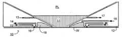
- FIG. 4A further immersion lithography solution with a localized liquid supply system is shown in FIG. 4 .
- Liquidis supplied by two groove inlets IN on either side of the projection system PL and is removed by a plurality of discrete outlets OUT arranged radially outwardly of the inlets IN.
- the inlets IN and OUTcan be arranged in a plate with a hole in its center and through which the projection beam is projected.
- Liquidis supplied by one groove inlet IN on one side of the projection system PL and removed by a plurality of discrete outlets OUT on the other side of the projection system PL, causing a flow of a thin film of liquid between the projection system PL and the substrate W.
- the choice of which combination of inlet IN and outlets OUT to usecan depend on the direction of movement of the substrate W (the other combination of inlet IN and outlets OUT being inactive).
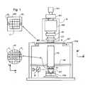
- FIG. 5Another immersion lithography solution with a localized liquid supply system solution which has been proposed is to provide the liquid supply system with a liquid confinement structure which extends along at least a part of a boundary of the space between the final element of the projection system and the substrate table.
- the liquid confinement structureis substantially stationary relative to the projection system in the XY plane though there may be some relative movement in the Z direction (in the direction of the optical axis).
- a sealis formed between the liquid confinement structure and the surface of the substrate.
- the sealis a contactless seal such as a gas seal.
- a liquid supply systemis used to supply liquid to the space between the final element of the projection system and the substrate.
- the reservoir 10forms a contactless seal to the substrate around the image field of the projection system so that liquid is confined to fill a space between the substrate surface and the final element of the projection system.
- the reservoiris formed by a liquid confinement structure 12 positioned below and surrounding the final element of the projection system PL.
- a first liquid 11is brought into the space below the projection system and within the liquid confinement structure 12 through supply 13 and removed by exhaust 17 .
- the liquid confinement structure 12extends a little above the final element of the projection system and the liquid level rises above the final element so that a buffer of liquid is provided.
- the liquid confinement structure 12has an inner periphery that at the upper end, in an embodiment, closely conforms to the shape of the projection system or the final element thereof and may, e.g., be round. At the bottom, the inner periphery may be circular or closely conform to the shape of the image field, e.g., rectangular.
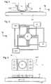
- the first liquid 11is confined in the reservoir by a second liquid 19 , with which it is substantially immiscible, that is supplied via supply 18 .
- the second liquid 19is confined by a gas seal 16 between the bottom of the liquid confinement structure 12 and the surface of the substrate W.
- the gas sealis formed by gas, e.g. air, synthetic air, N2 or an inert gas, provided under pressure via inlet 15 to the gap between liquid confinement structure 12 and substrate and extracted via first outlet 14 .
- the overpressure on the gas inlet 15 , vacuum level on the first outlet 14 and geometry of the gapare arranged so that there is a high-velocity gas flow inwards that confines the liquid.
- Other arrangements to confine a liquid while the body of liquid is moved over a substrate or the substrate is moved relative to the body of liquidare known and may be used to confine the second liquid and therefore also the first liquid.
- the first, or immersion, liquidis primarily selected on the basis of its optical properties, significantly its refractive index at the wavelength of the exposure radiation.
- Other useful properties of the second liquidare compatibility with the material of the final projection system element and with the resist, transmissivity and stability over time and under irradiation.
- deficiencies in these propertiescan in many cases be ameliorated by a coating on the final projection system element and/or the resist, by increasing the power of the radiation source and/or by increasing the refresh rate of the second liquid.
- Suitable compounds for the first liquidsare cycloalkanes, such as cyclooctane, decalin, bicyclohexyl, exo-tetrahydro-dicyclopentadiene and cyclohexane, other high-index hydrocarbons, perfluoropolyethers, such as perfluoro-N-methylmorpholine and Perfluoro E2, perfluoroalkanes, such as perfluorohexane, and hydrofluoroethers.
- cycloalkanessuch as cyclooctane, decalin, bicyclohexyl, exo-tetrahydro-dicyclopentadiene and cyclohexane
- other high-index hydrocarbonssuch as perfluoropolyethers, such as perfluoro-N-methylmorpholine and Perfluoro E2
- perfluoroalkanessuch as perfluorohexane
- significant fluid propertiesare those that enable it to be confined, such as surface tension, viscosity and interaction with surfaces of the liquid confinement structure, and its immiscibility with the second liquid.
- a suitable compound for the second liquidis water. Although a high refractive index is desirable, this and other optical properties of the liquid are relatively unimportant so that additives that increase the desirable properties of the first liquid can be chosen quite freely.
- the two liquidsare substantially immiscible and the functioning may be improved the less miscible are the two liquids.
- a sufficient degree of immiscibilitycan be obtained by selecting a non-polar liquid as the first liquid and a polar liquid as the second liquid. If the refractive index of the first and second liquids are not too different, a substantial amount of intermixing can be tolerated. For example, with water (refractive index 1.437) and a hydro-carbon of refractive index greater than 1.6, 1% by volume of water mixed with the hydrocarbon will only reduce the refractive index by only about 1 part in 1000.
- FIG. 6shows in plan, the outlines of the exposure field EF, the inner periphery 12 a of the liquid confinement structure 12 , the extent of the second liquid 19 and the outer periphery 12 b of the liquid confinement structure 12 .
- the inner periphery of the liquid confinement structure 12 amay be shaped, textured and or provided with coatings to stabilize the interface between the first and second liquids.
- a hydrophilic coatingmay be provided on the surface of the liquid confinement structure facing the substrate and a hydrophobic coating on the surface of the liquid confinement structure facing the space between the final element of the projection system and the substrate.
- water-related termssuch as hydrophilic, hydrophobic, humidity, etc. may be used herein, these terms should be understood to encompass the similar properties for other liquids.
- lithographic apparatusin the manufacture of ICs
- the lithographic apparatus described hereinmay have other applications, such as the manufacture of integrated optical systems, guidance and detection patterns for magnetic domain memories, flat-panel displays, liquid-crystal displays (LCDs), thin-film magnetic heads, etc.
- LCDsliquid-crystal displays
- any use of the terms “wafer” or “die” hereinmay be considered as synonymous with the more general terms “substrate” or “target portion”, respectively.
- the substrate referred to hereinmay be processed, before or after exposure, in for example a track (a tool that typically applies a layer of resist to a substrate and develops the exposed resist), a metrology tool and/or an inspection tool. Where applicable, the disclosure herein may be applied to such and other substrate processing tools. Further, the substrate may be processed more than once, for example in order to create a multi-layer IC, so that the term substrate used herein may also refer to a substrate that already contains multiple processed layers.
- UV radiatione.g. having a wavelength of or about 365, 248, 193, 157 or 126 nm.
- lensmay refer to any one or combination of various types of optical components, including refractive and reflective optical components.
- the inventionmay take the form of a computer program containing one or more sequences of machine-readable instructions describing a method as disclosed above, or a data storage medium (e.g. semiconductor memory, magnetic or optical disk) having such a computer program stored therein.
- a data storage mediume.g. semiconductor memory, magnetic or optical disk
- a liquid supply system as contemplated hereinshould be broadly construed. In certain embodiments, it may be a mechanism or combination of structures that provides a liquid to a space between the projection system and the substrate and/or substrate table. It may comprise a combination of one or more structures, one or more liquid inlets, one or more gas inlets, one or more gas outlets, and/or one or more liquid outlets that provide liquid to the space.
- a surface of the spacemay be a portion of the substrate and/or substrate table, or a surface of the space may completely cover a surface of the substrate and/or substrate table, or the space may envelop the substrate and/or substrate table.
- the liquid supply systemmay optionally further include one or more elements to control the position, quantity, quality, shape, flow rate or any other features of the liquid.
Landscapes
- Physics & Mathematics (AREA)
- General Physics & Mathematics (AREA)
- Health & Medical Sciences (AREA)
- Engineering & Computer Science (AREA)
- Environmental & Geological Engineering (AREA)
- Epidemiology (AREA)
- Public Health (AREA)
- Exposure And Positioning Against Photoresist Photosensitive Materials (AREA)
- Exposure Of Semiconductors, Excluding Electron Or Ion Beam Exposure (AREA)
Abstract
Description
- The present invention relates to a lithographic apparatus and a method for manufacturing a device.
- A lithographic apparatus is a machine that applies a desired pattern onto a substrate, usually onto a target portion of the substrate. A lithographic apparatus can be used, for example, in the manufacture of integrated circuits (ICs). In that instance, a patterning device, which is alternatively referred to as a mask or a reticle, may be used to generate a circuit pattern to be formed on an individual layer of the IC. This pattern can be transferred onto a target portion (e.g. comprising part of, one, or several dies) on a substrate (e.g. a silicon wafer). Transfer of the pattern is typically via imaging onto a layer of radiation-sensitive material (resist) provided on the substrate. In general, a single substrate will contain a network of adjacent target portions that are successively patterned. Known lithographic apparatus include so-called steppers, in which each target portion is irradiated by exposing an entire pattern onto the target portion at one time, and so-called scanners, in which each target portion is irradiated by scanning the pattern through a radiation beam in a given direction (the “scanning”-direction) while synchronously scanning the substrate parallel or anti-parallel to this direction. It is also possible to transfer the pattern from the patterning device to the substrate by imprinting the pattern onto the substrate.
- It has been proposed to immerse the substrate in the lithographic projection apparatus in a liquid having a relatively high refractive index, e.g. water, so as to fill a space between the final element of the projection system and the substrate. The point of this is to enable imaging of smaller features since the exposure radiation will have a shorter wavelength in the liquid. (The effect of the liquid may also be regarded as enabling the use of a larger effective NA of the system and also increasing the depth of focus.) Other immersion liquids have been proposed, including water with solid particles (e.g. quartz) suspended therein.
- However, submersing the substrate or substrate and substrate table in a bath of liquid (see, for example, U.S. Pat. No. 4,509,852, hereby incorporated in its entirety by reference) means that there is a large body of liquid that must be accelerated during a scanning exposure. This requires additional or more powerful motors and turbulence in the liquid may lead to undesirable and unpredictable effects.
- One of the solutions proposed is for a liquid supply system to provide liquid on only a localized area of the substrate and in between the final element of the projection system and the substrate using a liquid confinement system (the substrate generally has a larger surface area than the final element of the projection system). One way which has been proposed to arrange for this is disclosed in PCT patent application publication no. WO 99/49504, hereby incorporated in its entirety by reference. As illustrated in
FIGS. 2 and 3 , liquid is supplied by at least one inlet IN onto the substrate, preferably along the direction of movement of the substrate relative to the final element, and is removed by at least one outlet OUT after having passed under the projection system. That is, as the substrate is scanned beneath the element in a −X direction, liquid is supplied at the +X side of the element and taken up at the −X side.FIG. 2 shows the arrangement schematically in which liquid is supplied via inlet IN and is taken up on the other side of the element by outlet OUT which is connected to a low pressure source. In the illustration ofFIG. 2 the liquid is supplied along the direction of movement of the substrate relative to the final element, though this does not need to be the case. Various orientations and numbers of in- and out-lets positioned around the final element are possible, one example is illustrated inFIG. 3 in which four sets of an inlet with an outlet on either side are provided in a regular pattern around the final element. - The advantage provided by immersion lithography is dependent upon the refractive index of the immersion liquid—the higher the refractive index, the greater the benefit. Most existing proposals have used ultra pure water, which has a refractive index of 1.437 at 193 nm, as the immersion fluid but other fluids with higher refractive indexes have also been proposed. These include certain hydro-carbons that have a refractive index of greater than 1.6 at 193 nm, and certain perfluoropolyethers, which have a refractive index greater than 1.3 at 157 nm. Although these liquids are possibly suitable for immersion lithography—for example, they have good stability, transmissivity and are compatible with projection system materials and resists—their fluid properties are very different than those of water and so existing designs of liquid containment system may not effectively localize these fluids between the projection system and the substrate. These fluids are nonpolar and have very low surface tension so they easily spread out across the entire substrate and substrate table. Arrangements using gas knives that have been shown to successfully confine water, may not be able to confine these nonpolar fluids.
- Accordingly, it would advantageous, for example, to provide an immersion lithographic apparatus capable of localizing a nonpolar, low-surface tension liquid, e.g. to a space between the projection system and the substrate.
- According to an aspect of the invention, there is provided a lithographic projection apparatus, comprising:
- a projection system configured to project a patterned radiation beam onto a target portion of a substrate; and
- a liquid supply system configured to supplying a first liquid to a space between the projection system and the substrate, the liquid supply system comprising:
- a liquid confinement structure substantially surrounding the space and adapted to confine a liquid to a volume around the space;
- a first liquid supply arranged to supply the first liquid to the space; and
- a second liquid supply arranged to supply a second liquid to the volume.
- According to a further aspect of the invention, there is provided a device manufacturing method comprising projecting an image of a pattern through a liquid onto a target portion of a substrate using a projection system, wherein the liquid is confined to a space between the projection system and the substrate by a volume of another liquid.
- Embodiments of the invention will now be described, by way of example only, with reference to the accompanying schematic drawings in which corresponding reference symbols indicate corresponding parts, and in which:
FIG. 1 depicts a lithographic apparatus according to an embodiment of the invention;FIGS. 2 and 3 depict a liquid supply system for use in a lithographic projection apparatus;FIG. 4 depicts another liquid supply system for use in a lithographic projection apparatus;FIG. 5 depicts in cross-section the final element of a projection system and a liquid supply system in a lithographic apparatus according to an embodiment of the present invention; andFIG. 6 depicts in plan the liquid supply system ofFIG. 5 .FIG. 1 schematically depicts a lithographic apparatus according to an embodiment of the invention. The apparatus comprises:- an illumination system (illuminator) IL configured to condition a radiation beam B (e.g. UV radiation or DUV radiation).
- a support structure (e.g. a mask table) MT constructed to support a patterning device (e.g. a mask) MA and connected to a first positioner PM configured to accurately position the patterning device in accordance with certain parameters;
- a substrate table (e.g. a wafer table) WT constructed to hold a substrate (e.g. a resist-coated wafer) W and connected to a second positioner PW configured to accurately position the substrate in accordance with certain parameters; and
- a projection system (e.g. a refractive projection lens system) PS configured to project a pattern imparted to the radiation beam B by patterning device MA onto a target portion C (e.g. comprising one or more dies) of the substrate W.
- The illumination system may include various types of optical components, such as refractive, reflective, magnetic, electromagnetic, electrostatic or other types of optical components, or any combination thereof, for directing, shaping, or controlling radiation.
- The support structure holds the patterning device in a manner that depends on the orientation of the patterning device, the design of the lithographic apparatus, and other conditions, such as for example whether or not the patterning device is held in a vacuum environment. The support structure can use mechanical, vacuum, electrostatic or other clamping techniques to hold the patterning device. The support structure may be a frame or a table, for example, which may be fixed or movable as required. The support structure may ensure that the patterning device is at a desired position, for example with respect to the projection system. Any use of the terms “reticle” or “mask” herein may be considered synonymous with the more general term “patterning device.”
- The term “patterning device” used herein should be broadly interpreted as referring to any device that can be used to impart a radiation beam with a pattern in its cross-section such as to create a pattern in a target portion of the substrate. It should be noted that the pattern imparted to the radiation beam may not exactly correspond to the desired pattern in the target portion of the substrate, for example if the pattern includes phase-shifting features or so called assist features. Generally, the pattern imparted to the radiation beam will correspond to a particular functional layer in a device being created in the target portion, such as an integrated circuit.
- The patterning device may be transmissive or reflective. Examples of patterning devices include masks, programmable mirror arrays, and programmable LCD panels. Masks are well known in lithography, and include mask types such as binary, alternating phase-shift, and attenuated phase-shift, as well as various hybrid mask types. An example of a programmable mirror array employs a matrix arrangement of small mirrors, each of which can be individually tilted so as to reflect an incoming radiation beam in different directions. The tilted mirrors impart a pattern in a radiation beam which is reflected by the mirror matrix.
- The term “projection system” used herein should be broadly interpreted as encompassing any type of projection system, including refractive, reflective, catadioptric, magnetic, electromagnetic and electrostatic optical systems, or any combination thereof, as appropriate for the exposure radiation being used, or for other factors such as the use of an immersion liquid or the use of a vacuum. Any use of the term “projection lens” herein may be considered as synonymous with the more general term “projection system”.
- As here depicted, the apparatus is of a transmissive type (e.g. employing a transmissive mask). Alternatively, the apparatus may be of a reflective type (e.g. employing a programmable mirror array of a type as referred to above, or employing a reflective mask).
- The lithographic apparatus may be of a type having two (dual stage) or more substrate tables (and/or two or more mask tables). In such “multiple stage” machines the additional tables may be used in parallel, or preparatory steps may be carried out on one or more tables while one or more other tables are being used for exposure.
- Referring to
FIG. 1 , the illuminator IL receives a radiation beam from a radiation source SO. The source and the lithographic apparatus may be separate entities, for example when the source is an excimer laser. In such cases, the source is not considered to form part of the lithographic apparatus and the radiation beam is passed from the source SO to the illuminator IL with the aid of a beam delivery system BD comprising, for example, suitable directing mirrors and/or a beam expander. In other cases the source may be an integral part of the lithographic apparatus, for example when the source is a mercury lamp. The source SO and the illuminator IL, together with the beam delivery system BD if required, may be referred to as a radiation system. - The illuminator IL may comprise an adjuster AD for adjusting the angular intensity distribution of the radiation beam. Generally, at least the outer and/or inner radial extent (commonly referred to as σ-outer and σ-inner, respectively) of the intensity distribution in a pupil plane of the illuminator can be adjusted. In addition, the illuminator IL may comprise various other components, such as an integrator IN and a condenser CO. The illuminator may be used to condition the radiation beam, to have a desired uniformity and intensity distribution in its cross-section.
- The radiation beam B is incident on the patterning device (e.g., mask MA), which is held on the support structure (e.g., mask table MT), and is patterned by the patterning device. Having traversed the mask MA, the radiation beam B passes through the projection system PS, which focuses the beam onto a target portion C of the substrate W. With the aid of the second positioner PW and position sensor IF (e.g. an interferometric device, linear encoder or capacitive sensor), the substrate table WT can be moved accurately, e.g. so as to position different target portions C in the path of the radiation beam B. Similarly, the first positioner PM and another position sensor (which is not explicitly depicted in
FIG. 1 ) can be used to accurately position the mask MA with respect to the path of the radiation beam B, e.g. after mechanical retrieval from a mask library, or during a scan. In general, movement of the mask table MT may be realized with the aid of a long-stroke module (coarse positioning) and a short-stroke module (fine positioning), which form part of the first positioner PM. Similarly, movement of the substrate table WT may be realized using a long-stroke module and a shortstroke module, which form part of the second positioner PW. In the case of a stepper (as opposed to a scanner) the mask table MT may be connected to a short-stroke actuator only, or may be fixed. Mask MA and substrate W may be aligned using mask alignment marks M1, M2 and substrate alignment marks P1, P2. Although the substrate alignment marks as illustrated occupy dedicated target portions, they may be located in spaces between target portions (these are known as scribe-lane alignment marks). Similarly, in situations in which more than one die is provided on the mask MA, the mask alignment marks may be located between the dies. - The depicted apparatus could be used in at least one of the following modes:
- 1. In step mode, the mask table MT and the substrate table WT are kept essentially stationary, while an entire pattern imparted to the radiation beam is projected onto a target portion C at one time (i.e. a single static exposure). The substrate table WT is then shifted in the X and/or Y direction so that a different target portion C can be exposed. In step mode, the maximum size of the exposure field limits the size of the target portion C imaged in a single static exposure.
- 2. In scan mode, the mask table MT and the substrate table WT are scanned synchronously while a pattern imparted to the radiation beam is projected onto a target portion C (i.e. a single dynamic exposure). The velocity and direction of the substrate table WT relative to the mask table MT may be determined by the (de-)magnification and image reversal characteristics of the projection system PS. In scan mode, the maximum size of the exposure field limits the width (in the non-scanning direction) of the target portion in a single dynamic exposure, whereas the length of the scanning motion determines the height (in the scanning direction) of the target portion.
- 3. In another mode, the mask table MT is kept essentially stationary holding a programmable patterning device, and the substrate table WT is moved or scanned while a pattern imparted to the radiation beam is projected onto a target portion C. In this mode, generally a pulsed radiation source is employed and the programmable patterning device is updated as required after each movement of the substrate table WT or in between successive radiation pulses during a scan. This mode of operation can be readily applied to maskless lithography that utilizes programmable patterning device, such as a programmable mirror array of a type as referred to above.
- Combinations and/or variations on the above described modes of use or entirely different modes of use may also be employed.
- A further immersion lithography solution with a localized liquid supply system is shown in
FIG. 4 . Liquid is supplied by two groove inlets IN on either side of the projection system PL and is removed by a plurality of discrete outlets OUT arranged radially outwardly of the inlets IN. The inlets IN and OUT can be arranged in a plate with a hole in its center and through which the projection beam is projected. Liquid is supplied by one groove inlet IN on one side of the projection system PL and removed by a plurality of discrete outlets OUT on the other side of the projection system PL, causing a flow of a thin film of liquid between the projection system PL and the substrate W. The choice of which combination of inlet IN and outlets OUT to use can depend on the direction of movement of the substrate W (the other combination of inlet IN and outlets OUT being inactive). - Another immersion lithography solution with a localized liquid supply system solution which has been proposed is to provide the liquid supply system with a liquid confinement structure which extends along at least a part of a boundary of the space between the final element of the projection system and the substrate table. Such a solution is illustrated in
FIG. 5 . The liquid confinement structure is substantially stationary relative to the projection system in the XY plane though there may be some relative movement in the Z direction (in the direction of the optical axis). In an embodiment, a seal is formed between the liquid confinement structure and the surface of the substrate. In an embodiment, the seal is a contactless seal such as a gas seal. Such a system is disclosed in United States patent application publication no. US 2004-0207824 and European patent application publication no. EP 1420298, each hereby incorporated in its entirety by reference, and illustrated inFIG. 5 . - As shown in
FIG. 5 , a liquid supply system is used to supply liquid to the space between the final element of the projection system and the substrate. Thereservoir 10 forms a contactless seal to the substrate around the image field of the projection system so that liquid is confined to fill a space between the substrate surface and the final element of the projection system. The reservoir is formed by aliquid confinement structure 12 positioned below and surrounding the final element of the projection system PL. A first liquid11 is brought into the space below the projection system and within theliquid confinement structure 12 throughsupply 13 and removed byexhaust 17. Theliquid confinement structure 12 extends a little above the final element of the projection system and the liquid level rises above the final element so that a buffer of liquid is provided. Theliquid confinement structure 12 has an inner periphery that at the upper end, in an embodiment, closely conforms to the shape of the projection system or the final element thereof and may, e.g., be round. At the bottom, the inner periphery may be circular or closely conform to the shape of the image field, e.g., rectangular. - The first liquid11 is confined in the reservoir by a
second liquid 19, with which it is substantially immiscible, that is supplied viasupply 18. Thesecond liquid 19 is confined by agas seal 16 between the bottom of theliquid confinement structure 12 and the surface of the substrate W. The gas seal is formed by gas, e.g. air, synthetic air, N2 or an inert gas, provided under pressure via inlet15 to the gap betweenliquid confinement structure 12 and substrate and extracted viafirst outlet 14. The overpressure on the gas inlet15, vacuum level on thefirst outlet 14 and geometry of the gap are arranged so that there is a high-velocity gas flow inwards that confines the liquid. Other arrangements to confine a liquid while the body of liquid is moved over a substrate or the substrate is moved relative to the body of liquid are known and may be used to confine the second liquid and therefore also the first liquid. - The first, or immersion, liquid is primarily selected on the basis of its optical properties, significantly its refractive index at the wavelength of the exposure radiation. Other useful properties of the second liquid are compatibility with the material of the final projection system element and with the resist, transmissivity and stability over time and under irradiation. However deficiencies in these properties can in many cases be ameliorated by a coating on the final projection system element and/or the resist, by increasing the power of the radiation source and/or by increasing the refresh rate of the second liquid. Suitable compounds for the first liquids are cycloalkanes, such as cyclooctane, decalin, bicyclohexyl, exo-tetrahydro-dicyclopentadiene and cyclohexane, other high-index hydrocarbons, perfluoropolyethers, such as perfluoro-N-methylmorpholine and Perfluoro E2, perfluoroalkanes, such as perfluorohexane, and hydrofluoroethers.
- For the second, or confining, liquid, significant fluid properties are those that enable it to be confined, such as surface tension, viscosity and interaction with surfaces of the liquid confinement structure, and its immiscibility with the second liquid. A suitable compound for the second liquid is water. Although a high refractive index is desirable, this and other optical properties of the liquid are relatively unimportant so that additives that increase the desirable properties of the first liquid can be chosen quite freely.
- In an embodiment, the two liquids are substantially immiscible and the functioning may be improved the less miscible are the two liquids. A sufficient degree of immiscibility can be obtained by selecting a non-polar liquid as the first liquid and a polar liquid as the second liquid. If the refractive index of the first and second liquids are not too different, a substantial amount of intermixing can be tolerated. For example, with water (refractive index 1.437) and a hydro-carbon of refractive index greater than 1.6, 1% by volume of water mixed with the hydrocarbon will only reduce the refractive index by only about 1 part in 1000.
- The liquid confinement arrangement of this embodiment can be appreciated more clearly from
FIG. 6 which shows in plan, the outlines of the exposure field EF, theinner periphery 12aof theliquid confinement structure 12, the extent of thesecond liquid 19 and theouter periphery 12bof theliquid confinement structure 12. The inner periphery of theliquid confinement structure 12amay be shaped, textured and or provided with coatings to stabilize the interface between the first and second liquids. For example, where the first liquid is non-polar and the second liquid is water, a hydrophilic coating may be provided on the surface of the liquid confinement structure facing the substrate and a hydrophobic coating on the surface of the liquid confinement structure facing the space between the final element of the projection system and the substrate. - Although water-related terms such as hydrophilic, hydrophobic, humidity, etc. may be used herein, these terms should be understood to encompass the similar properties for other liquids.
- In European patent application publication no. EP 1420300 and United States patent application publication no. US 2004-0136494, each hereby incorporated in their entirety by reference, the idea of a twin or dual stage immersion lithography apparatus is disclosed. Such an apparatus is provided with two tables for supporting a substrate. Leveling measurements are carried out with a table at a first position, without immersion liquid, and exposure is carried out with a table at a second position, where immersion liquid is present. Alternatively, the apparatus has only one table.
- Although specific reference may be made in this text to the use of lithographic apparatus in the manufacture of ICs, it should be understood that the lithographic apparatus described herein may have other applications, such as the manufacture of integrated optical systems, guidance and detection patterns for magnetic domain memories, flat-panel displays, liquid-crystal displays (LCDs), thin-film magnetic heads, etc. The skilled artisan will appreciate that, in the context of such alternative applications, any use of the terms “wafer” or “die” herein may be considered as synonymous with the more general terms “substrate” or “target portion”, respectively. The substrate referred to herein may be processed, before or after exposure, in for example a track (a tool that typically applies a layer of resist to a substrate and develops the exposed resist), a metrology tool and/or an inspection tool. Where applicable, the disclosure herein may be applied to such and other substrate processing tools. Further, the substrate may be processed more than once, for example in order to create a multi-layer IC, so that the term substrate used herein may also refer to a substrate that already contains multiple processed layers.
- The terms “radiation” and “beam” used herein encompass all types of electromagnetic radiation, including ultraviolet (UV) radiation (e.g. having a wavelength of or about 365, 248, 193, 157 or 126 nm).
- The term “lens”, where the context allows, may refer to any one or combination of various types of optical components, including refractive and reflective optical components.
- While specific embodiments of the invention have been described above, it will be appreciated that the invention may be practiced otherwise than as described. For example, the invention may take the form of a computer program containing one or more sequences of machine-readable instructions describing a method as disclosed above, or a data storage medium (e.g. semiconductor memory, magnetic or optical disk) having such a computer program stored therein.
- One or more embodiments of the invention may be applied to any immersion lithography apparatus, in particular, but not exclusively, those types mentioned above and whether the immersion liquid is provided in the form of a bath or only on a localized surface area of the substrate. A liquid supply system as contemplated herein should be broadly construed. In certain embodiments, it may be a mechanism or combination of structures that provides a liquid to a space between the projection system and the substrate and/or substrate table. It may comprise a combination of one or more structures, one or more liquid inlets, one or more gas inlets, one or more gas outlets, and/or one or more liquid outlets that provide liquid to the space. In an embodiment, a surface of the space may be a portion of the substrate and/or substrate table, or a surface of the space may completely cover a surface of the substrate and/or substrate table, or the space may envelop the substrate and/or substrate table. The liquid supply system may optionally further include one or more elements to control the position, quantity, quality, shape, flow rate or any other features of the liquid.
- The descriptions above are intended to be illustrative, not limiting. Thus, it will be apparent to one skilled in the art that modifications may be made to the invention as described without departing from the scope of the claims set out below.
Claims (20)
Priority Applications (7)
| Application Number | Priority Date | Filing Date | Title |
|---|---|---|---|
| US11/120,198US7317507B2 (en) | 2005-05-03 | 2005-05-03 | Lithographic apparatus and device manufacturing method |
| TW095114173ATWI331705B (en) | 2005-05-03 | 2006-04-20 | Lithographic apparatus and device manufacturing method |
| JP2006123688AJP4543003B2 (en) | 2005-05-03 | 2006-04-27 | Lithographic apparatus and device manufacturing method |
| EP06252280AEP1720073B1 (en) | 2005-05-03 | 2006-04-28 | Device manufacturing method |
| SG200602940ASG126921A1 (en) | 2005-05-03 | 2006-05-02 | Lithographic apparatus and device manufacturing method |
| KR1020060040041AKR100706921B1 (en) | 2005-05-03 | 2006-05-03 | Lithographic apparatus and device manufacturing method |
| CN2006100778456ACN1858655B (en) | 2005-05-03 | 2006-05-08 | Lithographic apparatus and device manufacturing method |
Applications Claiming Priority (1)
| Application Number | Priority Date | Filing Date | Title |
|---|---|---|---|
| US11/120,198US7317507B2 (en) | 2005-05-03 | 2005-05-03 | Lithographic apparatus and device manufacturing method |
Publications (2)
| Publication Number | Publication Date |
|---|---|
| US20060250591A1true US20060250591A1 (en) | 2006-11-09 |
| US7317507B2 US7317507B2 (en) | 2008-01-08 |
Family
ID=36685649
Family Applications (1)
| Application Number | Title | Priority Date | Filing Date |
|---|---|---|---|
| US11/120,198Expired - Fee RelatedUS7317507B2 (en) | 2005-05-03 | 2005-05-03 | Lithographic apparatus and device manufacturing method |
Country Status (7)
| Country | Link |
|---|---|
| US (1) | US7317507B2 (en) |
| EP (1) | EP1720073B1 (en) |
| JP (1) | JP4543003B2 (en) |
| KR (1) | KR100706921B1 (en) |
| CN (1) | CN1858655B (en) |
| SG (1) | SG126921A1 (en) |
| TW (1) | TWI331705B (en) |
Cited By (12)
| Publication number | Priority date | Publication date | Assignee | Title |
|---|---|---|---|---|
| US20070004182A1 (en)* | 2005-06-30 | 2007-01-04 | Taiwan Semiconductor Manufacturing Company, Ltd. | Methods and system for inhibiting immersion lithography defect formation |
| US20070058263A1 (en)* | 2005-09-13 | 2007-03-15 | Taiwan Semiconductor Manufacturing Company, Ltd. | Apparatus and methods for immersion lithography |
| US20070091287A1 (en)* | 2005-10-24 | 2007-04-26 | Taiwan Semiconductor Manufacturing Company, Ltd. | Immersion lithography apparatus and methods |
| US20080002164A1 (en)* | 2006-06-29 | 2008-01-03 | Taiwan Semiconductor Manufacturing Company, Ltd. | Apparatus and method for immersion lithography |
| US20080129970A1 (en)* | 2005-01-25 | 2008-06-05 | Taiichi Furukawa | Immersion Exposure System, and Recycle Method and Supply Method of Liquid for Immersion Exposure |
| US20080304026A1 (en)* | 2007-03-02 | 2008-12-11 | Canon Kabushiki Kaisha | Immersion exposure apparatus and device manufacturing method |
| US20100060868A1 (en)* | 2008-09-02 | 2010-03-11 | Asml Netherlands B.V. | Fluid handling structure, lithographic apparatus and device manufactuirng method |
| KR100984713B1 (en) | 2007-08-02 | 2010-10-01 | 에이에스엠엘 네델란즈 비.브이. | Lithographic Apparatus and Device Manufacturing Method |
| US8692973B2 (en) | 2005-01-31 | 2014-04-08 | Nikon Corporation | Exposure apparatus and method for producing device |
| US8891059B2 (en) | 2007-01-23 | 2014-11-18 | Nikon Corporation | Liquid recovery system, immersion exposure apparatus, immersion exposing method, and device fabricating method |
| US9746781B2 (en) | 2005-01-31 | 2017-08-29 | Nikon Corporation | Exposure apparatus and method for producing device |
| US20200285036A1 (en)* | 2017-09-20 | 2020-09-10 | Max-Planck-Gesellschaft Zur Foerderung Der Wissenschaften E.V. | Cryo-Light Microscope and Immersion Medium for Cryo-Light Microscopy |
Families Citing this family (14)
| Publication number | Priority date | Publication date | Assignee | Title |
|---|---|---|---|---|
| TWI249082B (en)* | 2002-08-23 | 2006-02-11 | Nikon Corp | Projection optical system and method for photolithography and exposure apparatus and method using same |
| US7348575B2 (en) | 2003-05-06 | 2008-03-25 | Nikon Corporation | Projection optical system, exposure apparatus, and exposure method |
| EP2722703A3 (en) | 2003-05-06 | 2014-07-23 | Nikon Corporation | Projection optical system, and exposure apparatus and exposure method |
| TWI259319B (en)* | 2004-01-23 | 2006-08-01 | Air Prod & Chem | Immersion lithography fluids |
| US20050161644A1 (en)* | 2004-01-23 | 2005-07-28 | Peng Zhang | Immersion lithography fluids |
| KR20070029731A (en)* | 2004-06-01 | 2007-03-14 | 이 아이 듀폰 디 네모아 앤드 캄파니 | UV-transparent alkanes and their use in vacuum and far ultraviolet applications |
| WO2006130338A1 (en)* | 2005-06-01 | 2006-12-07 | Nikon Corporation | Immersion fluid containment system and method for immersion lithography |
| JP4804950B2 (en)* | 2005-09-26 | 2011-11-02 | 東京応化工業株式会社 | Method for measuring immersion lithography dissolved component of organic film |
| WO2007071280A1 (en)* | 2005-12-22 | 2007-06-28 | Freescale Semiconductor, Inc. | Immersion lithography apparatus and method of performing immersion lithography |
| US9632425B2 (en)* | 2006-12-07 | 2017-04-25 | Asml Holding N.V. | Lithographic apparatus, a dryer and a method of removing liquid from a surface |
| JP5055549B2 (en)* | 2007-03-22 | 2012-10-24 | 国立大学法人宇都宮大学 | Immersion exposure equipment |
| US9180524B2 (en)* | 2007-08-06 | 2015-11-10 | 3M Innovative Properties Company | Fly-cutting head, system and method, and tooling and sheeting produced therewith |
| CN104570618B (en)* | 2014-12-25 | 2016-08-17 | 浙江大学 | The immersion flow field sealing device on surface is replaced based on hydrophobe |
| CN104597720B (en)* | 2015-01-15 | 2016-08-17 | 浙江大学 | A kind of gas-liquid isolating device for immersed photoetching machine |
Citations (50)
| Publication number | Priority date | Publication date | Assignee | Title |
|---|---|---|---|---|
| US3573975A (en)* | 1968-07-10 | 1971-04-06 | Ibm | Photochemical fabrication process |
| US3648587A (en)* | 1967-10-20 | 1972-03-14 | Eastman Kodak Co | Focus control for optical instruments |
| US4346164A (en)* | 1980-10-06 | 1982-08-24 | Werner Tabarelli | Photolithographic method for the manufacture of integrated circuits |
| US4390273A (en)* | 1981-02-17 | 1983-06-28 | Censor Patent-Und Versuchsanstalt | Projection mask as well as a method and apparatus for the embedding thereof and projection printing system |
| US4396705A (en)* | 1980-09-19 | 1983-08-02 | Hitachi, Ltd. | Pattern forming method and pattern forming apparatus using exposures in a liquid |
| US4480910A (en)* | 1981-03-18 | 1984-11-06 | Hitachi, Ltd. | Pattern forming apparatus |
| US4509852A (en)* | 1980-10-06 | 1985-04-09 | Werner Tabarelli | Apparatus for the photolithographic manufacture of integrated circuit elements |
| US5040020A (en)* | 1988-03-31 | 1991-08-13 | Cornell Research Foundation, Inc. | Self-aligned, high resolution resonant dielectric lithography |
| US5121256A (en)* | 1991-03-14 | 1992-06-09 | The Board Of Trustees Of The Leland Stanford Junior University | Lithography system employing a solid immersion lens |
| US5610683A (en)* | 1992-11-27 | 1997-03-11 | Canon Kabushiki Kaisha | Immersion type projection exposure apparatus |
| US5825043A (en)* | 1996-10-07 | 1998-10-20 | Nikon Precision Inc. | Focusing and tilting adjustment system for lithography aligner, manufacturing apparatus or inspection apparatus |
| US5900354A (en)* | 1997-07-03 | 1999-05-04 | Batchelder; John Samuel | Method for optical inspection and lithography |
| US6236634B1 (en)* | 1996-08-26 | 2001-05-22 | Digital Papyrus Corporation | Method and apparatus for coupling an optical lens to a disk through a coupling medium having a relatively high index of refraction |
| US20020020821A1 (en)* | 2000-08-08 | 2002-02-21 | Koninklijke Philips Electronics N.V. | Method of manufacturing an optically scannable information carrier |
| US20020163629A1 (en)* | 2001-05-07 | 2002-11-07 | Michael Switkes | Methods and apparatus employing an index matching medium |
| US20030123040A1 (en)* | 2001-11-07 | 2003-07-03 | Gilad Almogy | Optical spot grid array printer |
| US6600547B2 (en)* | 2001-09-24 | 2003-07-29 | Nikon Corporation | Sliding seal |
| US6603130B1 (en)* | 1999-04-19 | 2003-08-05 | Asml Netherlands B.V. | Gas bearings for use with vacuum chambers and their application in lithographic projection apparatuses |
| US20040000627A1 (en)* | 2002-06-28 | 2004-01-01 | Carl Zeiss Semiconductor Manufacturing Technologies Ag | Method for focus detection and an imaging system with a focus-detection system |
| US20040075895A1 (en)* | 2002-10-22 | 2004-04-22 | Taiwan Semiconductor Manufacturing Co., Ltd. | Apparatus for method for immersion lithography |
| US20040114117A1 (en)* | 2002-11-18 | 2004-06-17 | Asml Netherlands B.V. | Lithographic apparatus and device manufacturing method |
| US20040136494A1 (en)* | 2002-11-12 | 2004-07-15 | Asml Netherlands B.V. | Lithographic apparatus and device manufacturing method |
| US20040160582A1 (en)* | 2002-11-12 | 2004-08-19 | Asml Netherlands B.V. | Lithographic apparatus and device manufacturing method |
| US20040165159A1 (en)* | 2002-11-12 | 2004-08-26 | Asml Netherlands B.V. | Lithographic apparatus and device manufacturing method |
| US20040207824A1 (en)* | 2002-11-12 | 2004-10-21 | Asml Netherlands B.V. | Lithographic apparatus and device manufacturing method |
| US20040211920A1 (en)* | 2002-11-12 | 2004-10-28 | Asml Netherlands B.V. | Lithographic apparatus and device manufacturing method |
| US20040239954A1 (en)* | 2003-05-28 | 2004-12-02 | Joerg Bischoff | Resolution enhanced optical metrology |
| US20040253547A1 (en)* | 2003-06-12 | 2004-12-16 | Matsushita Electric Industrial Co., Ltd. | Pattern formation method |
| US20040263809A1 (en)* | 2003-06-27 | 2004-12-30 | Canon Kabushiki Kaisha | Immersion exposure technique |
| US20050007569A1 (en)* | 2003-05-13 | 2005-01-13 | Asml Netherlands B.V. | Lithographic apparatus and device manufacturing method |
| US20050018155A1 (en)* | 2003-06-27 | 2005-01-27 | Asml Netherlands B. V. | Lithographic apparatus and device manufacturing method |
| US20050024609A1 (en)* | 2003-06-11 | 2005-02-03 | Asml Netherlands B.V. | Lithographic apparatus and device manufacturing method |
| US20050030497A1 (en)* | 2003-06-25 | 2005-02-10 | Takashi Nakamura | Liquid immersion type exposure apparatus |
| US20050046934A1 (en)* | 2003-08-29 | 2005-03-03 | Tokyo Electron Limited | Method and system for drying a substrate |
| US20050046813A1 (en)* | 2003-07-16 | 2005-03-03 | Asmil Netherlands B.V. | Lithographic apparatus and device manufacturing method |
| US20050052632A1 (en)* | 2003-09-09 | 2005-03-10 | Canon Kabushiki Kaisha | Exposure technique |
| US20050094116A1 (en)* | 2003-08-29 | 2005-05-05 | Asml Netherlands B.V. | Gradient immersion lithography |
| US20050094125A1 (en)* | 2003-10-31 | 2005-05-05 | Nikon Corporation | Supporting plate, stage device, exposure apparatus, and exposure method |
| US20050122505A1 (en)* | 2003-12-08 | 2005-06-09 | Canon Kabushiki Kaisha | Substrate-holding technique |
| US20050132914A1 (en)* | 2003-12-23 | 2005-06-23 | Asml Netherlands B.V. | Lithographic apparatus, alignment apparatus, device manufacturing method, and a method of converting an apparatus |
| US20050134817A1 (en)* | 2003-06-25 | 2005-06-23 | Takashi Nakamura | Liquid immersion type exposure apparatus |
| US20050140948A1 (en)* | 2003-12-26 | 2005-06-30 | Canon Kabushiki Kaisha | Exposure apparatus and method |
| US20050146694A1 (en)* | 2004-01-07 | 2005-07-07 | Toshinobu Tokita | Exposure apparatus and device manufacturing method |
| US20050146693A1 (en)* | 2003-12-09 | 2005-07-07 | Yoshinori Ohsaki | Exposure apparatus |
| US20050151942A1 (en)* | 2003-12-26 | 2005-07-14 | Canon Kabushiki Kaisha | Exposure method and apparatus |
| US20050200815A1 (en)* | 2004-02-09 | 2005-09-15 | Canon Kabushiki Kaisha | Projection exposure apparatus, device manufacturing method, and sensor unit |
| US20050213065A1 (en)* | 2004-03-29 | 2005-09-29 | Atsushi Kitaoka | Exposure apparatus and method |
| US20050213066A1 (en)* | 2004-03-29 | 2005-09-29 | Yuhei Sumiyoshi | Exposure apparatus |
| US20050219489A1 (en)* | 2002-12-10 | 2005-10-06 | Nikon Corporation | Exposure apparatus and method for producing device |
| US20050233081A1 (en)* | 2003-09-04 | 2005-10-20 | Toshinobu Tokita | Liquid immersion type exposure apparatus |
Family Cites Families (63)
| Publication number | Priority date | Publication date | Assignee | Title |
|---|---|---|---|---|
| DE224448C (en) | ||||
| DE242880C (en) | ||||
| DE206607C (en) | ||||
| DE221563C (en) | ||||
| ATE1462T1 (en) | 1979-07-27 | 1982-08-15 | Werner W. Dr. Tabarelli | OPTICAL LITHOGRAPHY PROCESS AND DEVICE FOR COPYING A PATTERN ONTO A SEMICONDUCTOR DISC. |
| FR2474708B1 (en) | 1980-01-24 | 1987-02-20 | Dme | HIGH-RESOLUTION MICROPHOTOLITHOGRAPHY PROCESS |
| JPS58202448A (en) | 1982-05-21 | 1983-11-25 | Hitachi Ltd | exposure equipment |
| JPS6265326A (en) | 1985-09-18 | 1987-03-24 | Hitachi Ltd | Exposure device |
| JPS62121417A (en) | 1985-11-22 | 1987-06-02 | Hitachi Ltd | Immersion objective lens device |
| JPS63157419A (en) | 1986-12-22 | 1988-06-30 | Toshiba Corp | Fine pattern transfer apparatus |
| JPH03209479A (en) | 1989-09-06 | 1991-09-12 | Sanee Giken Kk | Exposure method |
| JPH04305915A (en) | 1991-04-02 | 1992-10-28 | Nikon Corp | Adhesion type exposure device |
| JPH04305917A (en) | 1991-04-02 | 1992-10-28 | Nikon Corp | Close-contact exposure equipment |
| JPH06124873A (en) | 1992-10-09 | 1994-05-06 | Canon Inc | Immersion projection exposure system |
| JP2520833B2 (en) | 1992-12-21 | 1996-07-31 | 東京エレクトロン株式会社 | Immersion type liquid treatment device |
| JPH07220990A (en) | 1994-01-28 | 1995-08-18 | Hitachi Ltd | Pattern forming method and exposure apparatus thereof |
| JP3612920B2 (en) | 1997-02-14 | 2005-01-26 | ソニー株式会社 | Exposure apparatus for producing an optical recording medium master |
| JPH10255319A (en) | 1997-03-12 | 1998-09-25 | Hitachi Maxell Ltd | Master exposure apparatus and method |
| JP3747566B2 (en) | 1997-04-23 | 2006-02-22 | 株式会社ニコン | Immersion exposure equipment |
| JP3817836B2 (en) | 1997-06-10 | 2006-09-06 | 株式会社ニコン | EXPOSURE APPARATUS, ITS MANUFACTURING METHOD, EXPOSURE METHOD, AND DEVICE MANUFACTURING METHOD |
| JPH11176727A (en) | 1997-12-11 | 1999-07-02 | Nikon Corp | Projection exposure equipment |
| EP1039511A4 (en) | 1997-12-12 | 2005-03-02 | Nikon Corp | Projection exposure method and projection aligner |
| WO1999049504A1 (en) | 1998-03-26 | 1999-09-30 | Nikon Corporation | Projection exposure method and system |
| JP2000058436A (en) | 1998-08-11 | 2000-02-25 | Nikon Corp | Projection exposure apparatus and exposure method |
| JP4504479B2 (en) | 1999-09-21 | 2010-07-14 | オリンパス株式会社 | Immersion objective lens for microscope |
| AU2003218015A1 (en) | 2002-03-06 | 2003-09-22 | E.I. Du Pont De Nemours And Company | Fluorine-containing compounds with high transparency in the vacuum ultraviolet |
| WO2004053950A1 (en) | 2002-12-10 | 2004-06-24 | Nikon Corporation | Exposure apparatus and method for manufacturing device |
| DE10257766A1 (en) | 2002-12-10 | 2004-07-15 | Carl Zeiss Smt Ag | Method for setting a desired optical property of a projection lens and microlithographic projection exposure system |
| JP4232449B2 (en) | 2002-12-10 | 2009-03-04 | 株式会社ニコン | Exposure method, exposure apparatus, and device manufacturing method |
| WO2004053951A1 (en) | 2002-12-10 | 2004-06-24 | Nikon Corporation | Exposure method, exposure apparatus and method for manufacturing device |
| KR20120127755A (en) | 2002-12-10 | 2012-11-23 | 가부시키가이샤 니콘 | Exposure apparatus and method for manufacturing device |
| WO2004053955A1 (en) | 2002-12-10 | 2004-06-24 | Nikon Corporation | Exposure system and device producing method |
| EP1571694A4 (en) | 2002-12-10 | 2008-10-15 | Nikon Corp | Exposure apparatus and method for manufacturing device |
| AU2003289237A1 (en) | 2002-12-10 | 2004-06-30 | Nikon Corporation | Exposure apparatus and method for manufacturing device |
| JP4352874B2 (en) | 2002-12-10 | 2009-10-28 | 株式会社ニコン | Exposure apparatus and device manufacturing method |
| KR101101737B1 (en) | 2002-12-10 | 2012-01-05 | 가부시키가이샤 니콘 | Exposure apparatus, exposure method and method for manufacturing device |
| AU2003289272A1 (en) | 2002-12-10 | 2004-06-30 | Nikon Corporation | Surface position detection apparatus, exposure method, and device porducing method |
| KR20050085026A (en) | 2002-12-10 | 2005-08-29 | 가부시키가이샤 니콘 | Optical device and projection exposure apparatus using such optical device |
| EP1573730B1 (en) | 2002-12-13 | 2009-02-25 | Koninklijke Philips Electronics N.V. | Liquid removal in a method and device for irradiating spots on a layer |
| US7514699B2 (en) | 2002-12-19 | 2009-04-07 | Koninklijke Philips Electronics N.V. | Method and device for irradiating spots on a layer |
| EP1584089B1 (en) | 2002-12-19 | 2006-08-02 | Koninklijke Philips Electronics N.V. | Method and device for irradiating spots on a layer |
| EP2466623B1 (en) | 2003-02-26 | 2015-04-22 | Nikon Corporation | Exposure apparatus, exposure method, and method for producing device |
| WO2004093159A2 (en) | 2003-04-09 | 2004-10-28 | Nikon Corporation | Immersion lithography fluid control system |
| WO2004090633A2 (en) | 2003-04-10 | 2004-10-21 | Nikon Corporation | An electro-osmotic element for an immersion lithography apparatus |
| EP2950147B1 (en) | 2003-04-10 | 2017-04-26 | Nikon Corporation | Environmental system including vaccum scavenge for an immersion lithography apparatus |
| EP3352010A1 (en) | 2003-04-10 | 2018-07-25 | Nikon Corporation | Run-off path to collect liquid for an immersion lithography apparatus |
| EP3062152B1 (en) | 2003-04-10 | 2017-12-20 | Nikon Corporation | Environmental system including vaccum scavenge for an immersion lithography apparatus |
| CN101825847B (en) | 2003-04-11 | 2013-10-16 | 株式会社尼康 | Cleanup method for optics in immersion lithography |
| KR101225884B1 (en) | 2003-04-11 | 2013-01-28 | 가부시키가이샤 니콘 | Apparatus and method for maintaining immersion fluid in the gap under the projection lens during wafer exchange in an immersion lithography machine |
| JP4582089B2 (en) | 2003-04-11 | 2010-11-17 | 株式会社ニコン | Liquid jet recovery system for immersion lithography |
| SG194246A1 (en) | 2003-04-17 | 2013-11-29 | Nikon Corp | Optical arrangement of autofocus elements for use with immersion lithography |
| TWI421906B (en) | 2003-05-23 | 2014-01-01 | 尼康股份有限公司 | An exposure method, an exposure apparatus, and an element manufacturing method |
| US6867844B2 (en) | 2003-06-19 | 2005-03-15 | Asml Holding N.V. | Immersion photolithography system and method using microchannel nozzles |
| EP3179309A1 (en) | 2003-07-08 | 2017-06-14 | Nikon Corporation | Wafer table for immersion lithography |
| EP1500982A1 (en)* | 2003-07-24 | 2005-01-26 | ASML Netherlands B.V. | Lithographic apparatus and device manufacturing method |
| JP4333281B2 (en)* | 2003-08-28 | 2009-09-16 | 株式会社ニコン | Immersion optical system, liquid medium, and exposure apparatus |
| EP3223053A1 (en) | 2003-09-03 | 2017-09-27 | Nikon Corporation | Apparatus and method for providing fluid for immersion lithography |
| JP4444920B2 (en) | 2003-09-19 | 2010-03-31 | 株式会社ニコン | Exposure apparatus and device manufacturing method |
| SG144907A1 (en)* | 2003-09-29 | 2008-08-28 | Nikon Corp | Liquid immersion type lens system, projection exposure apparatus, and device fabricating method |
| US7352433B2 (en)* | 2003-10-28 | 2008-04-01 | Asml Netherlands B.V. | Lithographic apparatus and device manufacturing method |
| US7411653B2 (en)* | 2003-10-28 | 2008-08-12 | Asml Netherlands B.V. | Lithographic apparatus |
| EP1531362A3 (en) | 2003-11-13 | 2007-07-25 | Matsushita Electric Industrial Co., Ltd. | Semiconductor manufacturing apparatus and pattern formation method |
| TWI259319B (en) | 2004-01-23 | 2006-08-01 | Air Prod & Chem | Immersion lithography fluids |
- 2005
- 2005-05-03USUS11/120,198patent/US7317507B2/ennot_activeExpired - Fee Related
- 2006
- 2006-04-20TWTW095114173Apatent/TWI331705B/ennot_activeIP Right Cessation
- 2006-04-27JPJP2006123688Apatent/JP4543003B2/ennot_activeExpired - Fee Related
- 2006-04-28EPEP06252280Apatent/EP1720073B1/ennot_activeNot-in-force
- 2006-05-02SGSG200602940Apatent/SG126921A1/enunknown
- 2006-05-03KRKR1020060040041Apatent/KR100706921B1/ennot_activeExpired - Fee Related
- 2006-05-08CNCN2006100778456Apatent/CN1858655B/ennot_activeExpired - Fee Related
Patent Citations (52)
| Publication number | Priority date | Publication date | Assignee | Title |
|---|---|---|---|---|
| US3648587A (en)* | 1967-10-20 | 1972-03-14 | Eastman Kodak Co | Focus control for optical instruments |
| US3573975A (en)* | 1968-07-10 | 1971-04-06 | Ibm | Photochemical fabrication process |
| US4396705A (en)* | 1980-09-19 | 1983-08-02 | Hitachi, Ltd. | Pattern forming method and pattern forming apparatus using exposures in a liquid |
| US4346164A (en)* | 1980-10-06 | 1982-08-24 | Werner Tabarelli | Photolithographic method for the manufacture of integrated circuits |
| US4509852A (en)* | 1980-10-06 | 1985-04-09 | Werner Tabarelli | Apparatus for the photolithographic manufacture of integrated circuit elements |
| US4390273A (en)* | 1981-02-17 | 1983-06-28 | Censor Patent-Und Versuchsanstalt | Projection mask as well as a method and apparatus for the embedding thereof and projection printing system |
| US4480910A (en)* | 1981-03-18 | 1984-11-06 | Hitachi, Ltd. | Pattern forming apparatus |
| US5040020A (en)* | 1988-03-31 | 1991-08-13 | Cornell Research Foundation, Inc. | Self-aligned, high resolution resonant dielectric lithography |
| US5121256A (en)* | 1991-03-14 | 1992-06-09 | The Board Of Trustees Of The Leland Stanford Junior University | Lithography system employing a solid immersion lens |
| US5610683A (en)* | 1992-11-27 | 1997-03-11 | Canon Kabushiki Kaisha | Immersion type projection exposure apparatus |
| US6236634B1 (en)* | 1996-08-26 | 2001-05-22 | Digital Papyrus Corporation | Method and apparatus for coupling an optical lens to a disk through a coupling medium having a relatively high index of refraction |
| US5825043A (en)* | 1996-10-07 | 1998-10-20 | Nikon Precision Inc. | Focusing and tilting adjustment system for lithography aligner, manufacturing apparatus or inspection apparatus |
| US6191429B1 (en)* | 1996-10-07 | 2001-02-20 | Nikon Precision Inc. | Projection exposure apparatus and method with workpiece area detection |
| US5900354A (en)* | 1997-07-03 | 1999-05-04 | Batchelder; John Samuel | Method for optical inspection and lithography |
| US6603130B1 (en)* | 1999-04-19 | 2003-08-05 | Asml Netherlands B.V. | Gas bearings for use with vacuum chambers and their application in lithographic projection apparatuses |
| US20020020821A1 (en)* | 2000-08-08 | 2002-02-21 | Koninklijke Philips Electronics N.V. | Method of manufacturing an optically scannable information carrier |
| US20020163629A1 (en)* | 2001-05-07 | 2002-11-07 | Michael Switkes | Methods and apparatus employing an index matching medium |
| US6600547B2 (en)* | 2001-09-24 | 2003-07-29 | Nikon Corporation | Sliding seal |
| US20030123040A1 (en)* | 2001-11-07 | 2003-07-03 | Gilad Almogy | Optical spot grid array printer |
| US20040000627A1 (en)* | 2002-06-28 | 2004-01-01 | Carl Zeiss Semiconductor Manufacturing Technologies Ag | Method for focus detection and an imaging system with a focus-detection system |
| US20040075895A1 (en)* | 2002-10-22 | 2004-04-22 | Taiwan Semiconductor Manufacturing Co., Ltd. | Apparatus for method for immersion lithography |
| US20040211920A1 (en)* | 2002-11-12 | 2004-10-28 | Asml Netherlands B.V. | Lithographic apparatus and device manufacturing method |
| US20040136494A1 (en)* | 2002-11-12 | 2004-07-15 | Asml Netherlands B.V. | Lithographic apparatus and device manufacturing method |
| US20040160582A1 (en)* | 2002-11-12 | 2004-08-19 | Asml Netherlands B.V. | Lithographic apparatus and device manufacturing method |
| US20040165159A1 (en)* | 2002-11-12 | 2004-08-26 | Asml Netherlands B.V. | Lithographic apparatus and device manufacturing method |
| US20040207824A1 (en)* | 2002-11-12 | 2004-10-21 | Asml Netherlands B.V. | Lithographic apparatus and device manufacturing method |
| US20040114117A1 (en)* | 2002-11-18 | 2004-06-17 | Asml Netherlands B.V. | Lithographic apparatus and device manufacturing method |
| US20050219489A1 (en)* | 2002-12-10 | 2005-10-06 | Nikon Corporation | Exposure apparatus and method for producing device |
| US20050007569A1 (en)* | 2003-05-13 | 2005-01-13 | Asml Netherlands B.V. | Lithographic apparatus and device manufacturing method |
| US20040239954A1 (en)* | 2003-05-28 | 2004-12-02 | Joerg Bischoff | Resolution enhanced optical metrology |
| US20050024609A1 (en)* | 2003-06-11 | 2005-02-03 | Asml Netherlands B.V. | Lithographic apparatus and device manufacturing method |
| US20040253547A1 (en)* | 2003-06-12 | 2004-12-16 | Matsushita Electric Industrial Co., Ltd. | Pattern formation method |
| US20050134817A1 (en)* | 2003-06-25 | 2005-06-23 | Takashi Nakamura | Liquid immersion type exposure apparatus |
| US20050030497A1 (en)* | 2003-06-25 | 2005-02-10 | Takashi Nakamura | Liquid immersion type exposure apparatus |
| US20040263809A1 (en)* | 2003-06-27 | 2004-12-30 | Canon Kabushiki Kaisha | Immersion exposure technique |
| US20050018155A1 (en)* | 2003-06-27 | 2005-01-27 | Asml Netherlands B. V. | Lithographic apparatus and device manufacturing method |
| US20050046813A1 (en)* | 2003-07-16 | 2005-03-03 | Asmil Netherlands B.V. | Lithographic apparatus and device manufacturing method |
| US20050046934A1 (en)* | 2003-08-29 | 2005-03-03 | Tokyo Electron Limited | Method and system for drying a substrate |
| US20050094116A1 (en)* | 2003-08-29 | 2005-05-05 | Asml Netherlands B.V. | Gradient immersion lithography |
| US20050094119A1 (en)* | 2003-08-29 | 2005-05-05 | Asml Netherlands B.V. | Lithographic apparatus and device manufacturing method |
| US20050233081A1 (en)* | 2003-09-04 | 2005-10-20 | Toshinobu Tokita | Liquid immersion type exposure apparatus |
| US20050052632A1 (en)* | 2003-09-09 | 2005-03-10 | Canon Kabushiki Kaisha | Exposure technique |
| US20050094125A1 (en)* | 2003-10-31 | 2005-05-05 | Nikon Corporation | Supporting plate, stage device, exposure apparatus, and exposure method |
| US20050122505A1 (en)* | 2003-12-08 | 2005-06-09 | Canon Kabushiki Kaisha | Substrate-holding technique |
| US20050146693A1 (en)* | 2003-12-09 | 2005-07-07 | Yoshinori Ohsaki | Exposure apparatus |
| US20050132914A1 (en)* | 2003-12-23 | 2005-06-23 | Asml Netherlands B.V. | Lithographic apparatus, alignment apparatus, device manufacturing method, and a method of converting an apparatus |
| US20050140948A1 (en)* | 2003-12-26 | 2005-06-30 | Canon Kabushiki Kaisha | Exposure apparatus and method |
| US20050151942A1 (en)* | 2003-12-26 | 2005-07-14 | Canon Kabushiki Kaisha | Exposure method and apparatus |
| US20050146694A1 (en)* | 2004-01-07 | 2005-07-07 | Toshinobu Tokita | Exposure apparatus and device manufacturing method |
| US20050200815A1 (en)* | 2004-02-09 | 2005-09-15 | Canon Kabushiki Kaisha | Projection exposure apparatus, device manufacturing method, and sensor unit |
| US20050213065A1 (en)* | 2004-03-29 | 2005-09-29 | Atsushi Kitaoka | Exposure apparatus and method |
| US20050213066A1 (en)* | 2004-03-29 | 2005-09-29 | Yuhei Sumiyoshi | Exposure apparatus |
Cited By (18)
| Publication number | Priority date | Publication date | Assignee | Title |
|---|---|---|---|---|
| US20080129970A1 (en)* | 2005-01-25 | 2008-06-05 | Taiichi Furukawa | Immersion Exposure System, and Recycle Method and Supply Method of Liquid for Immersion Exposure |
| US8692973B2 (en) | 2005-01-31 | 2014-04-08 | Nikon Corporation | Exposure apparatus and method for producing device |
| US9746781B2 (en) | 2005-01-31 | 2017-08-29 | Nikon Corporation | Exposure apparatus and method for producing device |
| US20070004182A1 (en)* | 2005-06-30 | 2007-01-04 | Taiwan Semiconductor Manufacturing Company, Ltd. | Methods and system for inhibiting immersion lithography defect formation |
| US20070058263A1 (en)* | 2005-09-13 | 2007-03-15 | Taiwan Semiconductor Manufacturing Company, Ltd. | Apparatus and methods for immersion lithography |
| US20070091287A1 (en)* | 2005-10-24 | 2007-04-26 | Taiwan Semiconductor Manufacturing Company, Ltd. | Immersion lithography apparatus and methods |
| US7986395B2 (en) | 2005-10-24 | 2011-07-26 | Taiwan Semiconductor Manufacturing Company, Ltd. | Immersion lithography apparatus and methods |
| US20080002164A1 (en)* | 2006-06-29 | 2008-01-03 | Taiwan Semiconductor Manufacturing Company, Ltd. | Apparatus and method for immersion lithography |
| US8564759B2 (en) | 2006-06-29 | 2013-10-22 | Taiwan Semiconductor Manufacturing Company, Ltd. | Apparatus and method for immersion lithography |
| US8891059B2 (en) | 2007-01-23 | 2014-11-18 | Nikon Corporation | Liquid recovery system, immersion exposure apparatus, immersion exposing method, and device fabricating method |
| US20080304026A1 (en)* | 2007-03-02 | 2008-12-11 | Canon Kabushiki Kaisha | Immersion exposure apparatus and device manufacturing method |
| US7724350B2 (en) | 2007-03-02 | 2010-05-25 | Canon Kabushiki Kaisha | Immersion exposure apparatus and device manufacturing method |
| KR100984713B1 (en) | 2007-08-02 | 2010-10-01 | 에이에스엠엘 네델란즈 비.브이. | Lithographic Apparatus and Device Manufacturing Method |
| KR101376153B1 (en) | 2007-08-02 | 2014-03-27 | 에이에스엠엘 네델란즈 비.브이. | Lithographic apparatus and device manufacturing method |
| KR101056497B1 (en) | 2007-08-02 | 2011-08-11 | 에이에스엠엘 네델란즈 비.브이. | Lithographic Apparatus and Device Manufacturing Method |
| US20100060868A1 (en)* | 2008-09-02 | 2010-03-11 | Asml Netherlands B.V. | Fluid handling structure, lithographic apparatus and device manufactuirng method |
| US20200285036A1 (en)* | 2017-09-20 | 2020-09-10 | Max-Planck-Gesellschaft Zur Foerderung Der Wissenschaften E.V. | Cryo-Light Microscope and Immersion Medium for Cryo-Light Microscopy |
| US11754823B2 (en)* | 2017-09-20 | 2023-09-12 | MAX-PLANCK-Gesellschaft zur Förderung der Wissenschaften e.V. | Cryo-light microscope and immersion medium for cryo-light microscopy |
Also Published As
| Publication number | Publication date |
|---|---|
| KR100706921B1 (en) | 2007-04-13 |
| TW200643650A (en) | 2006-12-16 |
| EP1720073B1 (en) | 2012-01-18 |
| JP2006313905A (en) | 2006-11-16 |
| KR20060115613A (en) | 2006-11-09 |
| TWI331705B (en) | 2010-10-11 |
| CN1858655B (en) | 2010-09-01 |
| CN1858655A (en) | 2006-11-08 |
| EP1720073A1 (en) | 2006-11-08 |
| SG126921A1 (en) | 2006-11-29 |
| JP4543003B2 (en) | 2010-09-15 |
| US7317507B2 (en) | 2008-01-08 |
Similar Documents
| Publication | Publication Date | Title |
|---|---|---|
| EP1720073B1 (en) | Device manufacturing method | |
| US10353296B2 (en) | Lithographic apparatus and device manufacturing method | |
| US7808614B2 (en) | Lithographic apparatus and device manufacturing method | |
| US7812924B2 (en) | Lithographic apparatus and device manufacturing method | |
| US8564760B2 (en) | Lithographic apparatus, device manufacturing method and a control system | |
| US8456611B2 (en) | System and method to increase surface tension and contact angle in immersion lithography | |
| US9477159B2 (en) | Lithographic apparatus and device manufacturing method | |
| US10802410B2 (en) | Lithographic apparatus and device manufacturing method involving a barrier structure to handle liquid | |
| US9477153B2 (en) | Lithographic apparatus and device manufacturing method | |
| US7133114B2 (en) | Lithographic apparatus and device manufacturing method |
Legal Events
| Date | Code | Title | Description |
|---|---|---|---|
| AS | Assignment | Owner name:ASML NETHERLANDS B.V., NETHERLANDS Free format text:ASSIGNMENT OF ASSIGNORS INTEREST;ASSIGNOR:STRAAIJER, ALEXANDER;REEL/FRAME:016796/0649 Effective date:20050714 | |
| FEPP | Fee payment procedure | Free format text:PAYOR NUMBER ASSIGNED (ORIGINAL EVENT CODE: ASPN); ENTITY STATUS OF PATENT OWNER: LARGE ENTITY | |
| AS | Assignment | Owner name:ASML NETHERLANDS B.V., NETHERLANDS Free format text:ASSIGNMENT OF ASSIGNORS INTEREST;ASSIGNOR:STRAAIJER, ALEXANDER;REEL/FRAME:019220/0173 Effective date:20050714 | |
| STCF | Information on status: patent grant | Free format text:PATENTED CASE | |
| FPAY | Fee payment | Year of fee payment:4 | |
| FPAY | Fee payment | Year of fee payment:8 | |
| FEPP | Fee payment procedure | Free format text:MAINTENANCE FEE REMINDER MAILED (ORIGINAL EVENT CODE: REM.); ENTITY STATUS OF PATENT OWNER: LARGE ENTITY | |
| LAPS | Lapse for failure to pay maintenance fees | Free format text:PATENT EXPIRED FOR FAILURE TO PAY MAINTENANCE FEES (ORIGINAL EVENT CODE: EXP.); ENTITY STATUS OF PATENT OWNER: LARGE ENTITY | |
| STCH | Information on status: patent discontinuation | Free format text:PATENT EXPIRED DUE TO NONPAYMENT OF MAINTENANCE FEES UNDER 37 CFR 1.362 | |
| FP | Lapsed due to failure to pay maintenance fee | Effective date:20200108 |