US20060250513A1 - Image sensor with stabilized black level and low power consumption - Google Patents
Image sensor with stabilized black level and low power consumptionDownload PDFInfo
- Publication number
- US20060250513A1 US20060250513A1US11/484,741US48474106AUS2006250513A1US 20060250513 A1US20060250513 A1US 20060250513A1US 48474106 AUS48474106 AUS 48474106AUS 2006250513 A1US2006250513 A1US 2006250513A1
- Authority
- US
- United States
- Prior art keywords
- circuit
- read
- pixels
- period
- pixel
- Prior art date
- Legal status (The legal status is an assumption and is not a legal conclusion. Google has not performed a legal analysis and makes no representation as to the accuracy of the status listed.)
- Abandoned
Links
Images


Classifications
- H—ELECTRICITY
- H04—ELECTRIC COMMUNICATION TECHNIQUE
- H04N—PICTORIAL COMMUNICATION, e.g. TELEVISION
- H04N23/00—Cameras or camera modules comprising electronic image sensors; Control thereof
- H04N23/60—Control of cameras or camera modules
- H04N23/65—Control of camera operation in relation to power supply
- H04N23/651—Control of camera operation in relation to power supply for reducing power consumption by affecting camera operations, e.g. sleep mode, hibernation mode or power off of selective parts of the camera
- H—ELECTRICITY
- H04—ELECTRIC COMMUNICATION TECHNIQUE
- H04N—PICTORIAL COMMUNICATION, e.g. TELEVISION
- H04N25/00—Circuitry of solid-state image sensors [SSIS]; Control thereof
- H04N25/60—Noise processing, e.g. detecting, correcting, reducing or removing noise
- H04N25/616—Noise processing, e.g. detecting, correcting, reducing or removing noise involving a correlated sampling function, e.g. correlated double sampling [CDS] or triple sampling
- H—ELECTRICITY
- H04—ELECTRIC COMMUNICATION TECHNIQUE
- H04N—PICTORIAL COMMUNICATION, e.g. TELEVISION
- H04N25/00—Circuitry of solid-state image sensors [SSIS]; Control thereof
- H04N25/60—Noise processing, e.g. detecting, correcting, reducing or removing noise
- H04N25/63—Noise processing, e.g. detecting, correcting, reducing or removing noise applied to dark current
- H04N25/633—Noise processing, e.g. detecting, correcting, reducing or removing noise applied to dark current by using optical black pixels
- H—ELECTRICITY
- H04—ELECTRIC COMMUNICATION TECHNIQUE
- H04N—PICTORIAL COMMUNICATION, e.g. TELEVISION
- H04N25/00—Circuitry of solid-state image sensors [SSIS]; Control thereof
- H04N25/70—SSIS architectures; Circuits associated therewith
- H04N25/76—Addressed sensors, e.g. MOS or CMOS sensors
- H04N25/77—Pixel circuitry, e.g. memories, A/D converters, pixel amplifiers, shared circuits or shared components
- H—ELECTRICITY
- H04—ELECTRIC COMMUNICATION TECHNIQUE
- H04N—PICTORIAL COMMUNICATION, e.g. TELEVISION
- H04N25/00—Circuitry of solid-state image sensors [SSIS]; Control thereof
- H04N25/70—SSIS architectures; Circuits associated therewith
- H04N25/76—Addressed sensors, e.g. MOS or CMOS sensors
- H04N25/78—Readout circuits for addressed sensors, e.g. output amplifiers or A/D converters
Definitions
- the present inventionrelates generally to an image sensor, more particularly, to an image sensor having plurality of pixels arranged in rows and columns, for use in such an electronic camera, an image reader or a facsimile, with a stabilized black level and low power consumption.
- each light receiving elementoutputs a signal having an integrated light component and an integrated dark current component.
- This dark currenthas a strong temperature dependency that the current becomes about twice with rise of 9° C.
- the peripheral region of a pixel arraywas covered with a light shielding film to form an optical black pixel region, and an integrated dark current signal was read out from the optical black pixels in a blanking period to obtain the average voltage Vd of the integrated dark current signals in a black clamp circuit as an offset value (a black clamp level).
- the average Vdwas subtracted from each pixel signal Vs in the black clamp circuit in a period of reading out from an effective pixel region.
- black clampsThere are two kind of black clamps, one is a line black clamp performed in each horizontal scanning, the other is a frame black clamp performed in each frame, and one of them is adopted.
- FIG. 19shows an integrated dark current signal read out from an optical black pixel region in a horizontal blanking period.
- the signalis not constant according to characteristics of each pixel.
- the chip of an image sensorincludes an analogue circuit and a digital circuit
- power consumption of the analog circuitis larger than that of the digital circuit with a large ratio
- power consumption of an image sensor for taking a moving picturecannot decrease to a great extent by such methods.
- an object of the present inventionto provide an image sensor capable of preventing variations in black level due to a pixel defect.
- an image sensorcomprises a potential averaging line commonly connected to reset nodes of a plurality of pixels in a pixel row in a optical black pixel region.
- a potential averaging processingis automatically performed before reading out a signal from the optical black pixel region instead of performing an averaging processing in a black clamp circuit as in the prior art. Therefore, a black level (integrated dark current signal) is stabilized, more correct line black clamp is performed, and lateral stripe noise is reduced, thereby improving an image quality.
- an image sensorcomprising a control circuit for repeating sequential operation of a light integration period, a read-out period and a power-off period, wherein the control circuit: in the light integration period, causes the pixel array to perform light integration without supplying power to the read-out circuit; in the read-out period, causes the read-out circuit to read out the integrated signals; and in the power-off period, ceases to supply power to the pixel array and the read-out circuit.
- power supply for the read-out circuitceases in the light integration period and besides, power supply to the pixel array and the read-out circuit ceases in the power-off period, thereby power consumption in the image sensor can be reduced.
- FIG. 1is a schematic block diagram showing an image sensor of a first embodiment according to the present invention
- FIG. 2is a circuit diagram of part of the pixel array of FIG. 1 ;
- FIG. 3is a graph showing an integrated dark current signal (voltage) read out from an optical black pixel region in a horizontal blanking period
- FIG. 4is a schematic block diagram showing an image sensor of a second embodiment according to the present invention.
- FIG. 5is a schematic block diagram showing an image sensor of a third embodiment according to the present invention.
- FIG. 6is a schematic block diagram showing an image sensor of a fourth embodiment according to the present invention.
- FIG. 7is a circuit diagram showing the potential averaging line 30 A of FIG. 6 and part of its peripheral circuitry;
- FIG. 8is a schematic block diagram showing an image sensor of a fifth embodiment according to the present invention.
- FIG. 9is a circuit diagram showing the potential averaging lines 30 A to 30 D of FIG. 8 and part of their peripheral circuitry;
- FIG. 10is a schematic block diagram showing an image sensor of a sixth embodiment according to the present invention.
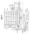
- FIG. 11is a schematic block diagram showing an image sensor of a seventh embodiment according to the present invention.
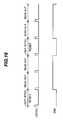
- FIG. 12is a time chart showing operation of the power source control circuit of FIG. 11 ;
- FIG. 13is a schematic block diagram showing an image sensor of an eighth embodiment according to the present invention.
- FIG. 14is a time chart showing operation of the power source control circuit of FIG. 13 ;
- FIG. 15is a schematic block diagram showing an image sensor of a ninth embodiment according to the present invention.
- FIG. 16is a time chart showing operation of the power source control circuit of FIG. 15 ;
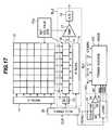
- FIG. 17is a schematic block diagram showing an image sensor of a tenth embodiment according to the present invention.
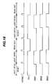
- FIG. 18is a time chart showing operation of the power source control circuit of FIG. 16 ;
- FIG. 19is a graph showing an integrated dark current signal read out from a prior art optical black pixel region in a horizontal blanking period.
- FIG. 1is a schematic block diagram showing an image sensor of a first embodiment according to the present invention.
- the image sensoris, for example, of a MOS type.
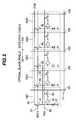
- a pixel array 10has pixels arranged in rows and columns.
- the hatched peripheral portion in the pixel array 10is an optical black pixel region 101 in which light receiving elements are covered with a light shielding film such as an aluminum film. Since light can not enter into the light receiving elements in the optical black pixel region 101 , only an integrated dark current signal is read out from this region.
- An area inside the optical black pixel region 101is an effective pixel region 102 with no light shielding film thereon.
- potential averaging lines 30 drawn with thick lines in FIG. 1are formed along pixel rows.
- Pixels of the optical black pixel region 101are the same as those of the effective pixel region 102 only with the exception that the light shielding film is formed above the pixels of the optical black pixel region 101 and the potential averaging lines 30 are formed in some pixels of the optical black pixel region.
- FIG. 2is a circuit diagram of part of a pixel array 10 of FIG. 1 .
- anode of a photodiode 31 as a light receiving elementis connected to grounded, while the cathode of the photodiode 31 is connected, on one hand, through a buffer amplifier 32 and a read-out switch element 33 to a vertical bus line 121 and, on the other hand, through a reset switch element 41 to a reset potential supply line 40 .
- the buffer amplifier 32is, for example, a source follower circuit.
- Each of the read-out switch element 33 and the reset switch 41is constituted of FET.
- Reset switch elements 42 to 45are provided in respective pixels 1022 to 1025 .
- the reset switch elements 42 to 45are connected between the cathodes of photodiodes and the reset potential supply line 40 .
- the control inputs of the read-out switch elements on the same roware commonly connected to a row select line 50 which is a gate line, and the control inputs of the reset switch elements 41 to 45 are commonly connected to a row reset line 51 which is a gate line.
- a row select signal RS 1 and a reset signal RST 1are provided from a vertical scanning circuit 11 of FIG. 1 .
- the reset ends (cathodes) of the photodiodes of the optical black pixels 1021 to 1023are commonly connected to the potential averaging line 30 drawn with a thick line.
- a read-out switch element 33is turned on by a pulse of the row select signal RS 1 and thereby the cathode potential of the photodiode 31 is read out through the buffer amplifier 32 and the read-out switch element 33 onto the vertical bus line 121 .
- the cathode potentials of the photodiodesare read out through buffer amplifiers and read-out switch elements onto the vertical bus lines 122 to 126 , respectively.
- the reset switches 41 to 45are turned on by a pulse of the reset signal RST 1 and the cathode potentials of the photodiodes are reset to VDD.
- Operations for read out and resetting on the pixels 1021 to 1025are performed every frame period. In one frame period from a reset to the next reset, electric charges accumulated in the photodiodes of the effective pixels 1024 and 1025 are discharged by incident light and dark current, while the electric charges in the optical black pixels 1021 to 1023 are discharged only by dark current.
- the vertical scanning circuit 11including a shift register sequentially activates row select lines on the pixel array 10 .
- signals integrated on light receiving elements on a selected roware read out onto the vertical bus 12 (vertical read out).
- the read-out signalsare held in respective sample and hold circuits 14 in response to activation of a control signal from a sample and hold control circuit 13 .
- the light receiving elements on the selected roware reset as described above to start integration again.
- CDScorrelation double sampling circuits
- the horizontal scanning circuit 15including a shift register sequentially activates the sample and hold circuits 14 from left to right in FIG. 1 to read out signals therefrom onto a horizontal bus 16 .
- the signal on the horizontal bus 16is amplified by the amplifier circuit 17 .
- the integrated dark current signalare read out onto the horizontal bus 16 during each horizontal blanking period and the voltage thereof is constant as shown in FIG. 3 . That is, since the voltage has been averaged prior to read out by the potential averaging line 30 , no averaging in the black clamp circuit 18 is required.
- the black clamp circuit 18samples the voltage, for example, at a time t 1 of FIG. 3 and holds the sampled voltage as a black clamp level Vb.
- the black clamp circuit 18subtracts the black clamp voltage Vb from the integrated voltage signal Vs on the horizontal bus 16 .
- Such a black level correcting operationis performed on each horizontal line and called as line black clamp.
- the black level corrected signalis converted to a digital value by an A/D converter circuit 19 .
- a timing control circuit 20generates control signals for operating the vertical scanning circuit 11 , the sample and hold circuit 13 and the horizontal scanning circuit 15 based on a clock signal CLK.
- the integrated dark current signals read out from the vertical bus lines 121 to 123are almost equal to one another. Differences among the integrated dark current signals on the optical black pixels 1021 to 1023 caused by variations in characteristics of the buffer amplifiers 32 and the read-out switch elements 33 are removed through the above described operation by the sample and hold circuits 14 .
- a potential averaging processis automatically performed prior to signal read out from the optical black pixel region 101 instead of an averaging process performed in the black clamp circuit 18 in the prior art, thereby stabilizing a read-out signal level.
- more correct line black clampis realized, thereby reducing lateral stripe noise to improve image quality.
- the construction of the black clamp circuit 18can be more simplified than that of the prior art.
- FIG. 4is a schematic block diagram showing an image sensor of a second embodiment according to the present invention.
- the black clamp levelcan be correctly sampled by the black clamp circuit 18 in this short period.
- the number of the sample and hold circuits 14 A and stages of a horizontal scanning circuits 15 Acan be smaller than that in the case of FIG. 1 .
- FIG. 5is a schematic block diagram showing an image sensor of a third embodiment according to the present invention.
- a mode signal MODEis provided to a horizontal scanning circuit 15 B.
- the circuit 15 Bscans from the left side to the right side in FIG. 5 when the mode signal MODE indicates a normal image mode, and scans in the opposite direction when the mode signal MODE indicates a left/right reverse image mode (or a top/bottom and left/right reverse image mode).
- the black clamp level for each horizontal lineis necessary to be determined prior to scanning effective pixels on the same line, potential averaging lines drawn with thick lines are formed on the both sides of the horizontal scanning lines.
- one vertical bus lineis connected to the signal input of end one of the sample and hold circuit 14 B.
- FIG. 6is a schematic block diagram showing an image sensor of a fourth embodiment according to the present invention.
- potential averaging lines 30 A to 30 Care provided on respective pixel rows on the vertical scanning start side in the optical black pixel region 101 .
- the number of sample and hold circuits 14 C and stages of a horizontal scanning circuit 15 Cis equal to the number of columns of the effective pixel region 102 and smaller than in the case of FIG. 4 by 1 . Further, the number of stages of a vertical scanning circuit 11 A is larger than that of rows of the effective pixel region 102 by the number of potential averaging lines.
- FIG. 7is a circuit diagram showing a potential averaging line 30 A of FIG. 6 and part of peripheral circuitry thereof.
- the black clamp circuit 18has an integration circuit for obtaining an average of voltages read out from potential averaging lines 30 A to 30 C each through a buffer amplifier, a read-out switch and a vertical bus line.
- the black clamp circuit 18holds the average as a black clamp level Vb and thereafter outputs the integrated light signal by subtracting the black clamp level Vb from the effective pixels' integrated signal Vs on the horizontal bus 16 .
- Such a black pixel correcting operationis performed every frame and called as frame black clamp.
- FIG. 8is a schematic block diagram showing an image sensor of a fifth embodiment according to the present invention.
- potential averaging lines 30 A to 30 Care connected to each other through a common line 30 D.
- FIG. 9shows potential averaging lines 30 A to 30 D of FIG. 8 and part of peripheral circuitry thereof.
- the potential averaging lines 30 A to 30 Dalso function as the reset potential supply line 40 of FIG. 2 . That is, the reset switch element 41 commonly used for three pixel rows is connected to the common line 30 D. Since an integrated dark current signal in common with the three pixel rows can be read out from each vertical bus line, the row select lines 50 A, 50 B and 50 C for the three pixel rows are also commonly connected to each other through a common line 50 D, and a row select signal RS 0 is provided to the common line 50 D to commonly turn on/off read-out switch elements for the three pixel rows.
- the number of stages of the vertical scanning circuit 11 Bis larger than the number of rows in the effective pixel region 102 by one, and the configuration thereof is thus simpler than that of the vertical scanning circuit 11 A of FIG. 6 .
- the black clamp period in the vertical blanking periodcan be 1 ⁇ 3 of that in the case of the fourth embodiment, the fifth embodiment is especially advantageous in a case where the number of pixels of the pixel array 10 is quite large and therefore the vertical blanking period is short.
- FIG. 10is a schematic block diagram showing an image sensor of a sixth embodiment according to the present invention.
- the mode signal MODEis provided to the vertical scanning circuit 11 D which scans from the top side to the bottom side in FIG. 10 when the mode signal MODE indicates a normal image mode, and scans in the opposite direction when the mode signal MODE indicates a top/bottom reverse image mode (or an top/bottom and left/right reverse image mode).
- one row select signal(commonly used for a plurality of rows) is connected to the output of the vertical scanning circuit 11 D.
- FIG. 11is a schematic block diagram showing an image sensor of a seventh embodiment according to the present invention.
- a reference voltage generating circuit 21 asupplies a reset voltage to the pixel array 10 and reference voltages to the sample and hold circuits 14 and the amplifier circuit 17 .
- the reference voltage generating circuit 21 ais a constituent of a power source circuit 21 .
- a mode signal MODEis provided to the power source circuit 21 , and the power source circuit 21 supplies power source voltages to circuits at all times when the mode signal indicate a normal mode.
- the power source circuit 21supplies the power source voltage to a block BL 1 during an enable signal EN 1 from a power source control circuit 22 is active and ceases the supply during the signal EN 1 is inactive, while supplying the power source voltages to a block BL 2 during an enable signal EN 2 from the power source control circuit 22 is active and ceases the supply during the signal EN 2 is inactive.
- the block BL 1includes the pixel array 10 and the vertical scanning circuit 11 .
- the block BL 2includes the sample and hold control circuit 13 , the sample and hold circuits 14 , the horizontal scanning circuit 15 , the amplifier circuit 17 and the A/D converter circuit 19 .
- the block BL 2includes the black clamp circuit as well, it is omitted for simplification and this applies in the below other embodiments.
- the power source circuit 21supplies a power source voltage to the timing control circuit 20 and the power source control circuit 22 at all times even in a low power consumption mode.
- the reference voltage generating circuit 21 aSince the reference voltage generating circuit 21 a is a constituent of the power source circuit 21 , the reference voltage generating circuit 21 a supplies the reset voltage to the pixel array 10 when the power source circuit 21 supplies the power source voltage to the block BL 1 , while the reference voltage generating circuit 21 a supplies the reference voltages to the sample and hold circuits 14 and the amplifier circuit 17 when the power source circuit 21 supplies the power source voltage to the block BL 2 .
- a vertical sync signal VSYNC from the timing control circuit 20is provided to the clock input of a counter 23 , the lowest bit Q 0 of the counter provides the enable signal EN 2 and the highest bit Q 1 of the counter 23 is provided to an inverter 24 to generate the enable signal EN 1 .
- the counter 23outputs counts 0, 1 and 2 cyclically and the enable signal EN 1 is high when the count is 0 or 1, while the enable signal EN 2 is high when the count is 1.
- FIG. 12is a time chart showing operation of the power source control circuit 22 of FIG. 11 .
- the count of the counter 23becomes 0 and the enable signal EN 1 goes high and the power source voltage is supplied to the block BL 1 .
- the pixel linesare sequentially activated by the vertical scanning circuit 11 in response to the control signal from the timing control circuit 20 . That is, the above described vertical read out and resetting are sequentially performed line by line. Since the power source voltages are not supplied to the block BL 2 , no power consumption thereof arises.
- the count of the counter 23becomes 1 and the enable signal EN 2 goes high and the power source voltages are also supplied to the block BL 2 .
- the pixel linesare sequentially activated and the vertical read out and resetting are performed line by line.
- the horizontal read outis performed each time after pixel signals from selected one row are latched in the sample and hold circuits 14 .
- operation in the read out periodis the same as that in the normal mode.
- the count of the counter 23becomes 2 and the enable signals EN 1 and EN 2 go low to cease the supply of the power source voltages to the blocks BL 1 and BL 2 .
- the periods of the light integration, the read out and the power-off described aboveare cyclically repeated.
- power supply to the block BL 2ceases in the light integration period and moreover, power supply to the blocks BL 1 and BL 2 ceases in the power-off period, therefore, in a 10 frame period for example, power consumption of the image sensor can be reduced to about 1 ⁇ 3 of that in the normal mode.
- FIG. 13is a schematic block diagram showing a image sensor of an eighth embodiment according to the present invention.
- a power source circuit 21 Asupplies its power source voltage to the pixel array 10 at all times even in the low power consumption mode.
- the power source circuit 21 Asupplies the power source voltage to the vertical scanning circuit 11 during an enable signal EN 1 A is active, while ceasing the supply during the enable signal EN 1 A is inactive.
- the output bit Q 0 of the counter 23is provided to the inverter 24 to generate the enable signal EN 1 A and the output bit Q 1 of the counter 23 provides an enable signal EN 2 .
- the other constituentsare the same as those of FIG. 11 .
- FIG. 14is a time chart showing operation of the power source control circuit 22 A of FIG. 13 .
- the enable signal EN 2goes low and supply of the power source voltage to the block BL 2 ceases.
- the vertical scanning circuit 11performs vertical scanning in response to the control signal from the timing control circuit 20 . Thereby, the above described read out and resetting are performed line by line.
- the count of the counter 23becomes 1 and the enable signal EN 1 A goes low and supply of the power source voltage to the vertical scanning circuit 11 ceases.
- the enable signals EN 1 and EN 2go high and the power source voltages are supplied to the blocks BL 1 and BL 2 .
- supply of the power source voltage to the block BL 2is cut off in the first and second light integration periods and the state is close to power-off. Therefore in a 15 frame periods for example, power consumption of the image sensor can be reduced to a value lower than 50% of that in the normal operation mode. Further, light integration periods are twice as long as in the first embodiment to improve sensitivity of the image sensor.
- the second light integration periodmay be a plurality of frames to increase the length of the light integration period by replacing the counter 23 of the power source control circuit 22 A with a scale-of-N counter, where N>3, and changing logic circuit configuration.
- FIG. 15is a schematic block diagram showing a image sensor of a ninth embodiment according to the present invention.
- a power source circuit 21 Bsupplies the power source voltage to the pixel array 10 and the vertical scanning circuit 11 at all times even in the low power consumption mode. Therefore, there is no need to provide the enable signal EN 1 to the power source circuit 21 B.
- a power source control circuit 22 Bthe output bits Q 0 and Q 1 of the counter 23 are provided to an OR gate 25 to generate the enable signal EN 2 .
- FIG. 16is a time chart showing operation of the power source control circuit 22 B of FIG. 15 .
- the count of the counter 23becomes 0 and the enable signal EN 2 goes low and supply of the power source voltage to the block BL 2 ceases.
- the vertical scanning circuit 11performs vertical scanning in response to the control signal from the timing control circuit 20 . Thereby, the above-described vertical read out and resetting are performed line by line.
- the count of the counter 23becomes 1 and the enable signal EN 2 goes high and the power source voltages are supplied to the block BL 2 .
- the count of the counter 23becomes 2 in response to the rising edge of the vertical sync signal VSYNC and the enable signal EN 2 remains high.
- the periods of such light integration, first read out and second read outare cyclically repeated.
- the stateis close to power-off and power consumption of the image sensor can be reduced to about 2 ⁇ 3 of that in the normal operation mode.
- a frame ratecan be increased to twice as large as that in the seventh embodiment.
- FIG. 17is a schematic block diagram showing an image sensor of a tenth embodiment according to the present invention.
- This image sensoris analogous to that of FIG. 11 but differs from the seventh embodiment in that the enable signal EN 2 of FIG. 11 is divided into enable signals EN 21 to EN 23 .
- a power source circuit 21 Csupplies the power source voltages as follows: during the enable signal EN 21 is active to the sample and hold control circuit 13 , the sample and hold circuits 14 and the horizontal scanning circuit 15 , during the enable signal EN 22 is active to the amplifier circuit 17 , and during the enable signal 23 is active to the A/D converter circuit 19 .
- a logic circuit 26In a power control circuit 22 C, a logic circuit 26 generates enable signals EN 21 to EN 23 shown in FIG. 18 according to the output bit Q 0 of the counter 23 and timing correction signals from the timing control circuit 20 . The rising and falling edges of the enable signals EN 21 to EN 23 are deviated a little from one another.
- the image sensormay be of a one-dimensional type.
- the power-off periodmay be two vertical scanning periods or longer if further reduced frame rate is no problem.
- the A/D converter circuit 19may be not constituent of the image sensor.
- amplifier circuits connected to respective vertical bus linesmay be employed.
- the image sensoris not limited to be of a MOS type but may be of such a CCD type.
Landscapes
- Engineering & Computer Science (AREA)
- Multimedia (AREA)
- Signal Processing (AREA)
- Transforming Light Signals Into Electric Signals (AREA)
- Facsimile Scanning Arrangements (AREA)
Abstract
Description
- 1. Field of the Invention
- The present invention relates generally to an image sensor, more particularly, to an image sensor having plurality of pixels arranged in rows and columns, for use in such an electronic camera, an image reader or a facsimile, with a stabilized black level and low power consumption.
- 2. Description of the Related Art
- In an image sensor, each light receiving element outputs a signal having an integrated light component and an integrated dark current component. This dark current has a strong temperature dependency that the current becomes about twice with rise of 9° C.
- In order to remove the integrated dark current component from the signal to obtain true integrated light signal, in the prior art, the peripheral region of a pixel array was covered with a light shielding film to form an optical black pixel region, and an integrated dark current signal was read out from the optical black pixels in a blanking period to obtain the average voltage Vd of the integrated dark current signals in a black clamp circuit as an offset value (a black clamp level). The average Vd was subtracted from each pixel signal Vs in the black clamp circuit in a period of reading out from an effective pixel region.
- There are two kind of black clamps, one is a line black clamp performed in each horizontal scanning, the other is a frame black clamp performed in each frame, and one of them is adopted.
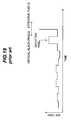
FIG. 19 shows an integrated dark current signal read out from an optical black pixel region in a horizontal blanking period. The signal is not constant according to characteristics of each pixel.- Especially, when a defective pixel exists, an integrated dark current signal suddenly changes as shown in
FIG. 19 , therefore an offset value becomes incorrect in a black clamp circuit having a integration capacitor for obtaining an average value, which causes lateral stripe noise. If the width of the optical black pixel region is wide in order to prevent the noise, the offset component could not be obtained in a horizontal blanking period in an image sensor having quite many pixels, or a chip area increases with the result of higher cost. - On the other hand, in an image sensor adopted in portable equipment, reduction in power consumption has been required.
- There are following methods for reduction in power consumption of a semiconductor chip:
- (1) to stop an operation clock in a period where no operation is required; and
- (2) to reduce a clock frequency by a divider, for example, to a half, a quarter and one-eighths thereof.
- However, the chip of an image sensor includes an analogue circuit and a digital circuit, power consumption of the analog circuit is larger than that of the digital circuit with a large ratio, and power consumption of an image sensor for taking a moving picture cannot decrease to a great extent by such methods.
- When a power source for the analog circuit is on/off controlled, the influence of off appears after one frame, therefore the power source cannot be simply turned off.
- Accordingly, it is an object of the present invention to provide an image sensor capable of preventing variations in black level due to a pixel defect.
- It is another object of the present invention to provide an image sensor capable of obtaining a black clamp level in a shorter time.
- It is still another object of the present invention to provide an image sensor capable of decreasing power consumption by performing fine on/off control of a power source for an internal circuit in a case of a reduced frame rate.
- In one aspect of the present invention, an image sensor comprises a potential averaging line commonly connected to reset nodes of a plurality of pixels in a pixel row in a optical black pixel region.
- With this aspect, a potential averaging processing is automatically performed before reading out a signal from the optical black pixel region instead of performing an averaging processing in a black clamp circuit as in the prior art. Therefore, a black level (integrated dark current signal) is stabilized, more correct line black clamp is performed, and lateral stripe noise is reduced, thereby improving an image quality.
- Further, since an integrated dark current signal has only to be sampled at a specific time, a configuration of a black clamp circuit can be made simpler than that in the prior art.
- Furthermore, since a black clamp level (an offset value) can be obtained in a shorter time than in the prior art because of the above described reason, there is no problem even if quite many pixels exist in a pixel array and thereby a blanking period is short.
- In another aspect of the present invention, there is provided an image sensor comprising a control circuit for repeating sequential operation of a light integration period, a read-out period and a power-off period, wherein the control circuit: in the light integration period, causes the pixel array to perform light integration without supplying power to the read-out circuit; in the read-out period, causes the read-out circuit to read out the integrated signals; and in the power-off period, ceases to supply power to the pixel array and the read-out circuit.
- With this aspect, power supply for the read-out circuit ceases in the light integration period and besides, power supply to the pixel array and the read-out circuit ceases in the power-off period, thereby power consumption in the image sensor can be reduced.
- Other aspects, objects, and the advantages of the present invention will become apparent from the following detailed description taken in connection with the accompanying drawings.
FIG. 1 is a schematic block diagram showing an image sensor of a first embodiment according to the present invention;FIG. 2 is a circuit diagram of part of the pixel array ofFIG. 1 ;FIG. 3 is a graph showing an integrated dark current signal (voltage) read out from an optical black pixel region in a horizontal blanking period;FIG. 4 is a schematic block diagram showing an image sensor of a second embodiment according to the present invention;FIG. 5 is a schematic block diagram showing an image sensor of a third embodiment according to the present invention;FIG. 6 is a schematic block diagram showing an image sensor of a fourth embodiment according to the present invention;FIG. 7 is a circuit diagram showing the potentialaveraging line 30A ofFIG. 6 and part of its peripheral circuitry;FIG. 8 is a schematic block diagram showing an image sensor of a fifth embodiment according to the present invention;FIG. 9 is a circuit diagram showing the potentialaveraging lines 30A to30D ofFIG. 8 and part of their peripheral circuitry;FIG. 10 is a schematic block diagram showing an image sensor of a sixth embodiment according to the present invention;FIG. 11 is a schematic block diagram showing an image sensor of a seventh embodiment according to the present invention;FIG. 12 is a time chart showing operation of the power source control circuit ofFIG. 11 ;FIG. 13 is a schematic block diagram showing an image sensor of an eighth embodiment according to the present invention;FIG. 14 is a time chart showing operation of the power source control circuit ofFIG. 13 ;FIG. 15 is a schematic block diagram showing an image sensor of a ninth embodiment according to the present invention;FIG. 16 is a time chart showing operation of the power source control circuit ofFIG. 15 ;FIG. 17 is a schematic block diagram showing an image sensor of a tenth embodiment according to the present invention;FIG. 18 is a time chart showing operation of the power source control circuit ofFIG. 16 ; andFIG. 19 is a graph showing an integrated dark current signal read out from a prior art optical black pixel region in a horizontal blanking period.- Referring now to the drawings, wherein like reference characters designate like or corresponding parts throughout several views, preferred embodiments of the present invention are described below.
FIG. 1 is a schematic block diagram showing an image sensor of a first embodiment according to the present invention.- The image sensor is, for example, of a MOS type.
- A
pixel array 10 has pixels arranged in rows and columns. The hatched peripheral portion in thepixel array 10 is an opticalblack pixel region 101 in which light receiving elements are covered with a light shielding film such as an aluminum film. Since light can not enter into the light receiving elements in the opticalblack pixel region 101, only an integrated dark current signal is read out from this region. An area inside the opticalblack pixel region 101 is aneffective pixel region 102 with no light shielding film thereon. - In the horizontal scanning start side of the optical
black pixel region 101 and beneath the light shielding film, potentialaveraging lines 30 drawn with thick lines inFIG. 1 are formed along pixel rows. - Pixels of the optical
black pixel region 101 are the same as those of theeffective pixel region 102 only with the exception that the light shielding film is formed above the pixels of the opticalblack pixel region 101 and the potentialaveraging lines 30 are formed in some pixels of the optical black pixel region. FIG. 2 is a circuit diagram of part of apixel array 10 ofFIG. 1 .- In an optical
black pixel 1021, the anode of aphotodiode 31 as a light receiving element is connected to grounded, while the cathode of thephotodiode 31 is connected, on one hand, through abuffer amplifier 32 and a read-out switch element 33 to avertical bus line 121 and, on the other hand, through areset switch element 41 to a resetpotential supply line 40. Thebuffer amplifier 32 is, for example, a source follower circuit. Each of the read-out switch element 33 and thereset switch 41 is constituted of FET.Reset switch elements 42 to45 are provided inrespective pixels 1022 to1025. Thereset switch elements 42 to45 are connected between the cathodes of photodiodes and the resetpotential supply line 40. - The control inputs of the read-out switch elements on the same row are commonly connected to a row
select line 50 which is a gate line, and the control inputs of thereset switch elements 41 to45 are commonly connected to arow reset line 51 which is a gate line. To the rowselect line 50 and the row resetline 51, a row select signal RS1 and a reset signal RST1, respectively, are provided from avertical scanning circuit 11 ofFIG. 1 . The reset ends (cathodes) of the photodiodes of the opticalblack pixels 1021 to1023 are commonly connected to thepotential averaging line 30 drawn with a thick line. - A read-
out switch element 33 is turned on by a pulse of the row select signal RS1 and thereby the cathode potential of thephotodiode 31 is read out through thebuffer amplifier 32 and the read-out switch element 33 onto thevertical bus line 121. Similarly, in regard to thepixels 1022 to1025, the cathode potentials of the photodiodes are read out through buffer amplifiers and read-out switch elements onto thevertical bus lines 122 to126, respectively. Then, the reset switches41 to45 are turned on by a pulse of the reset signal RST1 and the cathode potentials of the photodiodes are reset to VDD. - Operations for read out and resetting on the
pixels 1021 to1025 are performed every frame period. In one frame period from a reset to the next reset, electric charges accumulated in the photodiodes of theeffective pixels black pixels 1021 to1023 are discharged only by dark current. - Referring back to
FIG. 1 , thevertical scanning circuit 11 including a shift register sequentially activates row select lines on thepixel array 10. Thereby, signals integrated on light receiving elements on a selected row are read out onto the vertical bus12 (vertical read out). The read-out signals are held in respective sample and holdcircuits 14 in response to activation of a control signal from a sample and holdcontrol circuit 13. The light receiving elements on the selected row are reset as described above to start integration again. - The sample and hold
circuits 14 are, for example, correlation double sampling circuits (CDS) and in this case, read out and holding of each integrated signal will be detailed as follows. Firstly, the sample and holdcircuits 14 are reset. Then a voltage (an integrated signal Vx)+(a component DV depending on variation of characteristic of thebuffer amplifier 32 and the read-out switch element 33 coupled to the photodiode31) is sampled to corresponding one of the sample and holdcircuits 14. Next the resetting is performed at the pixel on the selected row. Thereafter, a second sampling is performed to hold the difference Vx=(Vx+DV)−DV in the corresponding one of the sample and holdcircuits 14. - The
horizontal scanning circuit 15 including a shift register sequentially activates the sample and holdcircuits 14 from left to right inFIG. 1 to read out signals therefrom onto ahorizontal bus 16. The signal on thehorizontal bus 16 is amplified by theamplifier circuit 17. - The integrated dark current signal are read out onto the
horizontal bus 16 during each horizontal blanking period and the voltage thereof is constant as shown inFIG. 3 . That is, since the voltage has been averaged prior to read out by thepotential averaging line 30, no averaging in theblack clamp circuit 18 is required. Theblack clamp circuit 18 samples the voltage, for example, at a time t1 ofFIG. 3 and holds the sampled voltage as a black clamp level Vb. When reading out an integrated signal from an effective pixel, theblack clamp circuit 18 subtracts the black clamp voltage Vb from the integrated voltage signal Vs on thehorizontal bus 16. Such a black level correcting operation is performed on each horizontal line and called as line black clamp. - The black level corrected signal is converted to a digital value by an A/
D converter circuit 19. - A
timing control circuit 20 generates control signals for operating thevertical scanning circuit 11, the sample and holdcircuit 13 and thehorizontal scanning circuit 15 based on a clock signal CLK. - Referring back to
FIG. 2 , in the opticalblack pixels 1021 to1023, since the reset ends of the photodiodes are commonly connected to thepotential averaging line 30, the integrated dark current signals read out from thevertical bus lines 121 to123 are almost equal to one another. Differences among the integrated dark current signals on the opticalblack pixels 1021 to1023 caused by variations in characteristics of thebuffer amplifiers 32 and the read-out switch elements 33 are removed through the above described operation by the sample and holdcircuits 14. - In the first embodiment, since a reset node in each pixel on the same row in the optical
black pixel region 101 is commonly connected to thepotential averaging line 30, a potential averaging process is automatically performed prior to signal read out from the opticalblack pixel region 101 instead of an averaging process performed in theblack clamp circuit 18 in the prior art, thereby stabilizing a read-out signal level. Hence, more correct line black clamp is realized, thereby reducing lateral stripe noise to improve image quality. - Further, since the integrated dark current signal has only to be sampled at a specific time, the construction of the
black clamp circuit 18 can be more simplified than that of the prior art. FIG. 4 is a schematic block diagram showing an image sensor of a second embodiment according to the present invention.- In this image sensor, among the vertical bus lines in the optical
black pixel region 101, only thevertical line 123 ofFIG. 2 is connected to the signal input of one of sample and holdcircuits 14A. - Thereby, even when the number of pixels in the
pixel array 10 is quite large and in turn the horizontal blanking period is short, the black clamp level can be correctly sampled by theblack clamp circuit 18 in this short period. - Further, the number of the sample and hold
circuits 14A and stages of ahorizontal scanning circuits 15A can be smaller than that in the case ofFIG. 1 . - The other points are the same as that of the first embodiment.
FIG. 5 is a schematic block diagram showing an image sensor of a third embodiment according to the present invention.- In this image sensor, a mode signal MODE is provided to a
horizontal scanning circuit 15B. Thecircuit 15B scans from the left side to the right side inFIG. 5 when the mode signal MODE indicates a normal image mode, and scans in the opposite direction when the mode signal MODE indicates a left/right reverse image mode (or a top/bottom and left/right reverse image mode). - The black clamp level for each horizontal line is necessary to be determined prior to scanning effective pixels on the same line, potential averaging lines drawn with thick lines are formed on the both sides of the horizontal scanning lines. In each of the both sides, one vertical bus line is connected to the signal input of end one of the sample and hold
circuit 14B. - The other points are the same as that of the second embodiment.
FIG. 6 is a schematic block diagram showing an image sensor of a fourth embodiment according to the present invention.- In this image sensor, in order to perform frame black clamp,
potential averaging lines 30A to30C are provided on respective pixel rows on the vertical scanning start side in the opticalblack pixel region 101. - The number of sample and hold
circuits 14C and stages of ahorizontal scanning circuit 15C is equal to the number of columns of theeffective pixel region 102 and smaller than in the case ofFIG. 4 by1. Further, the number of stages of avertical scanning circuit 11A is larger than that of rows of theeffective pixel region 102 by the number of potential averaging lines. FIG. 7 is a circuit diagram showing apotential averaging line 30A ofFIG. 6 and part of peripheral circuitry thereof.- In
FIG. 6 , theblack clamp circuit 18 has an integration circuit for obtaining an average of voltages read out frompotential averaging lines 30A to30C each through a buffer amplifier, a read-out switch and a vertical bus line. Theblack clamp circuit 18 holds the average as a black clamp level Vb and thereafter outputs the integrated light signal by subtracting the black clamp level Vb from the effective pixels' integrated signal Vs on thehorizontal bus 16. Such a black pixel correcting operation is performed every frame and called as frame black clamp. - In the fourth embodiment, a similar effect as that of the first embodiment is obtained.
FIG. 8 is a schematic block diagram showing an image sensor of a fifth embodiment according to the present invention.- In this image sensor,
potential averaging lines 30A to30C are connected to each other through acommon line 30D. FIG. 9 showspotential averaging lines 30A to30D ofFIG. 8 and part of peripheral circuitry thereof.- The
potential averaging lines 30A to30D also function as the resetpotential supply line 40 ofFIG. 2 . That is, thereset switch element 41 commonly used for three pixel rows is connected to thecommon line 30D. Since an integrated dark current signal in common with the three pixel rows can be read out from each vertical bus line, the row select lines50A,50B and50C for the three pixel rows are also commonly connected to each other through acommon line 50D, and a row select signal RS0 is provided to thecommon line 50D to commonly turn on/off read-out switch elements for the three pixel rows. - Since only the row select signal RS0 is sufficient for the three pixel rows, the number of stages of the
vertical scanning circuit 11B is larger than the number of rows in theeffective pixel region 102 by one, and the configuration thereof is thus simpler than that of thevertical scanning circuit 11A ofFIG. 6 . - Further, since the black clamp period in the vertical blanking period can be ⅓ of that in the case of the fourth embodiment, the fifth embodiment is especially advantageous in a case where the number of pixels of the
pixel array 10 is quite large and therefore the vertical blanking period is short. - The other points are the same as that of the fourth embodiment.
FIG. 10 is a schematic block diagram showing an image sensor of a sixth embodiment according to the present invention.- In this image sensor, the mode signal MODE is provided to the
vertical scanning circuit 11D which scans from the top side to the bottom side inFIG. 10 when the mode signal MODE indicates a normal image mode, and scans in the opposite direction when the mode signal MODE indicates a top/bottom reverse image mode (or an top/bottom and left/right reverse image mode). - Since the black clamp level for each frame is necessary to be determined prior to scanning effective pixels on the same frame, potential averaging lines drawn with thick lines are formed on the both sides of the vertical scanning.
- In each sides, one row select signal (commonly used for a plurality of rows) is connected to the output of the
vertical scanning circuit 11D. - The other points are the same as that of the fifth embodiment.
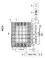
FIG. 11 is a schematic block diagram showing an image sensor of a seventh embodiment according to the present invention.- A reference
voltage generating circuit 21asupplies a reset voltage to thepixel array 10 and reference voltages to the sample and holdcircuits 14 and theamplifier circuit 17. The referencevoltage generating circuit 21ais a constituent of apower source circuit 21. - A mode signal MODE is provided to the
power source circuit 21, and thepower source circuit 21 supplies power source voltages to circuits at all times when the mode signal indicate a normal mode. Thepower source circuit 21 supplies the power source voltage to a block BL1 during an enable signal EN1 from a powersource control circuit 22 is active and ceases the supply during the signal EN1 is inactive, while supplying the power source voltages to a block BL2 during an enable signal EN2 from the powersource control circuit 22 is active and ceases the supply during the signal EN2 is inactive. - The block BL1 includes the
pixel array 10 and thevertical scanning circuit 11. The block BL2 includes the sample and holdcontrol circuit 13, the sample and holdcircuits 14, thehorizontal scanning circuit 15, theamplifier circuit 17 and the A/D converter circuit 19. Although the block BL2 includes the black clamp circuit as well, it is omitted for simplification and this applies in the below other embodiments. - The
power source circuit 21 supplies a power source voltage to thetiming control circuit 20 and the powersource control circuit 22 at all times even in a low power consumption mode. - Since the reference
voltage generating circuit 21ais a constituent of thepower source circuit 21, the referencevoltage generating circuit 21asupplies the reset voltage to thepixel array 10 when thepower source circuit 21 supplies the power source voltage to the block BL1, while the referencevoltage generating circuit 21asupplies the reference voltages to the sample and holdcircuits 14 and theamplifier circuit 17 when thepower source circuit 21 supplies the power source voltage to the block BL2. - In the power
source control circuit 22, a vertical sync signal VSYNC from thetiming control circuit 20 is provided to the clock input of acounter 23, the lowest bit Q0 of the counter provides the enable signal EN2 and the highest bit Q1 of thecounter 23 is provided to aninverter 24 to generate the enable signal EN1. Thecounter 23 outputs counts 0, 1 and 2 cyclically and the enable signal EN1 is high when the count is 0 or 1, while the enable signal EN2 is high when the count is 1. FIG. 12 is a time chart showing operation of the powersource control circuit 22 ofFIG. 11 .- Next, description will be given of operation of the image sensor configured as described above in a case of low power consumption mode.
- In an initial state, assume that the count of the
counter 23 is 2. In this state, the power source voltages are supplied to neither of the blocks BL1 and BL2. - (Light Integration Period)
- In response to the rising edge of the vertical sync signal VSYNC, the count of the
counter 23 becomes 0 and the enable signal EN1 goes high and the power source voltage is supplied to the block BL1. - The pixel lines are sequentially activated by the
vertical scanning circuit 11 in response to the control signal from thetiming control circuit 20. That is, the above described vertical read out and resetting are sequentially performed line by line. Since the power source voltages are not supplied to the block BL2, no power consumption thereof arises. - (Reading-Out Period)
- In response to the rising edge of a vertical sync signal VSYNC, the count of the
counter 23 becomes 1 and the enable signal EN2 goes high and the power source voltages are also supplied to the block BL2. - In the block BL1, the pixel lines are sequentially activated and the vertical read out and resetting are performed line by line. In the block BL2, the horizontal read out is performed each time after pixel signals from selected one row are latched in the sample and hold
circuits 14. - That is, operation in the read out period is the same as that in the normal mode.
- (Power-Off Period)
- In response to the rising edge of a vertical sync signal VSYNC, the count of the
counter 23 becomes 2 and the enable signals EN1 and EN2 go low to cease the supply of the power source voltages to the blocks BL1 and BL2. - The periods of the light integration, the read out and the power-off described above are cyclically repeated.
- Consumed currents are, for example, as follows:
- about 1 mA into the
pixel array 10, - about 3 mA in total to the
vertical scanning circuit 11, the sample and holdcontrol circuits 13, thehorizontal scanning circuit 15, thetiming control circuit 20 and the powersource control circuit 22, - about 2.5 mA into the sample and hold
circuits 14, - about 8 mA into the
amplifier circuit 17, - about 12 mA into the A/
D converter circuit 19, - about 0.5 mA into the reference
voltage generating circuit 21a, and - about 22.5 mA in total to the sample and hold
circuits 14, theamplifier circuit 17 and the A/D converter circuit 19 in the block BL2, wherein this current is comparatively large. - According to this seventh embodiment, power supply to the block BL2 ceases in the light integration period and moreover, power supply to the blocks BL1 and BL2 ceases in the power-off period, therefore, in a 10 frame period for example, power consumption of the image sensor can be reduced to about ⅓ of that in the normal mode.
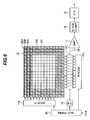
FIG. 13 is a schematic block diagram showing a image sensor of an eighth embodiment according to the present invention.- A
power source circuit 21A supplies its power source voltage to thepixel array 10 at all times even in the low power consumption mode. - In the low power consumption mode, the
power source circuit 21A supplies the power source voltage to thevertical scanning circuit 11 during an enable signal EN1A is active, while ceasing the supply during the enable signal EN1A is inactive. - In a power
source control circuit 22A, the output bit Q0 of thecounter 23 is provided to theinverter 24 to generate the enable signal EN1A and the output bit Q1 of thecounter 23 provides an enable signal EN2. - The other constituents are the same as those of FIG.11.
FIG. 14 is a time chart showing operation of the powersource control circuit 22A ofFIG. 13 .- Next, description will be given of operation of the image sensor configured as describe above in a case of the low power consumption mode.
- In an initial state, assume that the count of the
counter 23 is 2. In this state, the power source voltages are supplied to thevertical scanning circuit 11 and the block BL2. - (First Light Integration Period)
- In response to the rising edge of the vertical sync signal VSYNC, the count of the
counter 23 becomes 0, the enable signal EN2 goes low and supply of the power source voltage to the block BL2 ceases. - The
vertical scanning circuit 11 performs vertical scanning in response to the control signal from thetiming control circuit 20. Thereby, the above described read out and resetting are performed line by line. - (Second Light Integration Period)
- In response to the rising edge of the vertical sync signal VSYNC, the count of the
counter 23 becomes 1 and the enable signal EN1A goes low and supply of the power source voltage to thevertical scanning circuit 11 ceases. - Thereby, only the light integration is performed in the
pixel array 10. - (Reading-Out Period)
- In response to the rising edge of the vertical sync signal VSYNC, the count of the
counter 23 becomes 2, the enable signals EN1 and EN2 go high and the power source voltages are supplied to the blocks BL1 and BL2. - Thereby, the same operation as read out in the seventh embodiment is performed.
- The periods of first and second light integration and reading-out described above are cyclically repeated.
- According to this eight embodiment, supply of the power source voltage to the block BL2 is cut off in the first and second light integration periods and the state is close to power-off. Therefore in a 15 frame periods for example, power consumption of the image sensor can be reduced to a value lower than 50% of that in the normal operation mode. Further, light integration periods are twice as long as in the first embodiment to improve sensitivity of the image sensor.
- Note that the second light integration period may be a plurality of frames to increase the length of the light integration period by replacing the
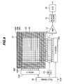
counter 23 of the powersource control circuit 22A with a scale-of-N counter, where N>3, and changing logic circuit configuration. FIG. 15 is a schematic block diagram showing a image sensor of a ninth embodiment according to the present invention.- A
power source circuit 21B supplies the power source voltage to thepixel array 10 and thevertical scanning circuit 11 at all times even in the low power consumption mode. Therefore, there is no need to provide the enable signal EN1 to thepower source circuit 21B. - In a power
source control circuit 22B, the output bits Q0 and Q1 of thecounter 23 are provided to anOR gate 25 to generate the enable signal EN2. - The other constituents are the same as that of
FIG. 11 . FIG. 16 is a time chart showing operation of the powersource control circuit 22B ofFIG. 15 .- Next, description will be given of operation of the image sensor configured as described above in the case of the low power consumption mode.
- In an initial state, assume that the count of the
counter 23 is 2. In this state, the power source voltage is supplied to the block BL2. - (Light Integration Period)
- In response to the rising edge of the vertical sync signal VSYNC, the count of the
counter 23 becomes 0 and the enable signal EN2 goes low and supply of the power source voltage to the block BL2 ceases. - The
vertical scanning circuit 11 performs vertical scanning in response to the control signal from thetiming control circuit 20. Thereby, the above-described vertical read out and resetting are performed line by line. - (First Read Out Period)
- In response to the rising edge of the vertical sync signal VSYNC, the count of the
counter 23 becomes 1 and the enable signal EN2 goes high and the power source voltages are supplied to the block BL2. - Thereby, the same operation as the read out in the seventh embodiment is performed.
- (Second Read Out Period)
- The count of the
counter 23 becomes 2 in response to the rising edge of the vertical sync signal VSYNC and the enable signal EN2 remains high. - Thereby, the same operation as the read out described above is performed.
- The periods of such light integration, first read out and second read out are cyclically repeated.
- According to this ninth embodiment, since supply of the power source voltages to the block BL2 are cut off in the light integration period, the state is close to power-off and power consumption of the image sensor can be reduced to about ⅔ of that in the normal operation mode. Moreover, since read out is performed in two of three frames, a frame rate can be increased to twice as large as that in the seventh embodiment.
FIG. 17 is a schematic block diagram showing an image sensor of a tenth embodiment according to the present invention.- This image sensor is analogous to that of
FIG. 11 but differs from the seventh embodiment in that the enable signal EN2 ofFIG. 11 is divided into enable signals EN21 to EN23. - In the low power consumption mode, a
power source circuit 21C supplies the power source voltages as follows: during the enable signal EN21 is active to the sample and holdcontrol circuit 13, the sample and holdcircuits 14 and thehorizontal scanning circuit 15, during the enable signal EN22 is active to theamplifier circuit 17, and during the enablesignal 23 is active to the A/D converter circuit 19. - In a
power control circuit 22C, alogic circuit 26 generates enable signals EN21 to EN23 shown inFIG. 18 according to the output bit Q0 of thecounter 23 and timing correction signals from thetiming control circuit 20. The rising and falling edges of the enable signals EN21 to EN23 are deviated a little from one another. - The other constituents are the same as that of
FIG. 11 . - Description of operation of the above-described configuration is omitted since it is apparent from the description of the seventh embodiment and
FIG. 18 . - According to this tenth embodiment, since a sudden change in current is reduced due to the deviations of the rising and falling edges of the enable signals EN21 to EN23, variations in the power source voltage are smaller than in the seventh embodiment.
- Although preferred embodiments of the present invention has been described, it is to be understood that the invention is not limited thereto and that various changes and modifications may be made without departing from the spirit and scope of the invention.
- For example, in the first to tenth embodiments, the image sensor may be of a one-dimensional type.
- In the seventh embodiment, the power-off period may be two vertical scanning periods or longer if further reduced frame rate is no problem.
- Further, the A/
D converter circuit 19 may be not constituent of the image sensor. In stead of theamplifier circuit 17 connected to thehorizontal bus 16, amplifier circuits connected to respective vertical bus lines may be employed. The image sensor is not limited to be of a MOS type but may be of such a CCD type.
Claims (10)
Priority Applications (1)
| Application Number | Priority Date | Filing Date | Title |
|---|---|---|---|
| US11/484,741US20060250513A1 (en) | 2000-03-28 | 2006-07-12 | Image sensor with stabilized black level and low power consumption |
Applications Claiming Priority (6)
| Application Number | Priority Date | Filing Date | Title |
|---|---|---|---|
| JP2000-092971 | 2000-03-28 | ||
| JP2000092967AJP3827502B2 (en) | 2000-03-28 | 2000-03-28 | Image sensor |
| JP2000-092967 | 2000-03-28 | ||
| JP2000092971AJP3904366B2 (en) | 2000-03-28 | 2000-03-28 | Image sensor |
| US09/785,330US7098950B2 (en) | 2000-03-28 | 2001-02-20 | Image sensor with stabilized black level and low power consumption |
| US11/484,741US20060250513A1 (en) | 2000-03-28 | 2006-07-12 | Image sensor with stabilized black level and low power consumption |
Related Parent Applications (1)
| Application Number | Title | Priority Date | Filing Date |
|---|---|---|---|
| US09/785,330DivisionUS7098950B2 (en) | 2000-03-28 | 2001-02-20 | Image sensor with stabilized black level and low power consumption |
Publications (1)
| Publication Number | Publication Date |
|---|---|
| US20060250513A1true US20060250513A1 (en) | 2006-11-09 |
Family
ID=26588805
Family Applications (2)
| Application Number | Title | Priority Date | Filing Date |
|---|---|---|---|
| US09/785,330Expired - Fee RelatedUS7098950B2 (en) | 2000-03-28 | 2001-02-20 | Image sensor with stabilized black level and low power consumption |
| US11/484,741AbandonedUS20060250513A1 (en) | 2000-03-28 | 2006-07-12 | Image sensor with stabilized black level and low power consumption |
Family Applications Before (1)
| Application Number | Title | Priority Date | Filing Date |
|---|---|---|---|
| US09/785,330Expired - Fee RelatedUS7098950B2 (en) | 2000-03-28 | 2001-02-20 | Image sensor with stabilized black level and low power consumption |
Country Status (3)
| Country | Link |
|---|---|
| US (2) | US7098950B2 (en) |
| EP (1) | EP1143706A3 (en) |
| KR (1) | KR100736188B1 (en) |
Cited By (15)
| Publication number | Priority date | Publication date | Assignee | Title |
|---|---|---|---|---|
| US20040125421A1 (en)* | 2002-09-19 | 2004-07-01 | Canon Kabushiki Kaisha | Image pickup apparatus |
| US20060197857A1 (en)* | 2002-02-01 | 2006-09-07 | Barna Sandor L | CMOS image sensor with a low-power architecture |
| US20070279503A1 (en)* | 2006-05-01 | 2007-12-06 | Canon Kabushiki Kaisha | Image pickup apparatus and image reading apparatus using image pickup apparatus |
| US20100053379A1 (en)* | 2007-05-21 | 2010-03-04 | Trygve Willassen | Suppression of Row-Wise Noise in CMOS Image Sensors |
| US20110254960A1 (en)* | 2010-02-15 | 2011-10-20 | Ulrich Seger | Image converter |
| US20120013780A1 (en)* | 2010-07-19 | 2012-01-19 | Aptina Imaging Corporation | Optical black pixel cell readout systems and methods |
| US20120293697A1 (en)* | 2011-05-16 | 2012-11-22 | Himax Imaging, Inc. | Image Sensor and Control Method for Image Sensor |
| WO2014018948A3 (en)* | 2012-07-26 | 2014-08-07 | Olive Medical Corporation | Camera system with minimal area monolithic cmos image sensor |
| US20140368708A1 (en)* | 2013-06-18 | 2014-12-18 | Samsung Electronics Co., Ltd. | Image sensor, image signal processor and electronic device including the same |
| US8952312B2 (en) | 2011-05-12 | 2015-02-10 | Olive Medical Corporation | Image sensor for endoscopic use |
| US20160122639A1 (en)* | 2011-06-06 | 2016-05-05 | Saint-Gobain Ceramics & Plastics, Inc. | Method of forming a scintillation crystal including a rare earth halide |
| US9971440B2 (en) | 2010-03-12 | 2018-05-15 | Semiconductor Energy Laboratory Co., Ltd. | Method for driving circuit and method for driving display device |
| US10203421B2 (en) | 2012-10-28 | 2019-02-12 | Stichting Voor De Technische Wetenschappen | Method of forming a scintillation crystal and a radiation detection apparatus including a scintillation crystal including a rare earth halide |
| US10517469B2 (en) | 2013-03-15 | 2019-12-31 | DePuy Synthes Products, Inc. | Image sensor synchronization without input clock and data transmission clock |
| US10750933B2 (en) | 2013-03-15 | 2020-08-25 | DePuy Synthes Products, Inc. | Minimize image sensor I/O and conductor counts in endoscope applications |
Families Citing this family (55)
| Publication number | Priority date | Publication date | Assignee | Title |
|---|---|---|---|---|
| KR100530258B1 (en)* | 2005-04-26 | 2005-11-22 | 엠텍비젼 주식회사 | Method and apparatus for compensating black level by dark current of image sensor |
| JP2001339643A (en)* | 2000-05-30 | 2001-12-07 | Nec Corp | Black level generation circuit for solid-state imaging device and solid-state imaging device |
| US7038820B1 (en)* | 2002-04-03 | 2006-05-02 | Eastman Kodak Company | Automatic exposure control for an image sensor |
| KR100517548B1 (en)* | 2002-07-30 | 2005-09-28 | 삼성전자주식회사 | Analog to didital converter for cmos image device |
| KR20040017862A (en)* | 2002-08-22 | 2004-03-02 | 삼성전자주식회사 | Analog-digital converter for image sensor |
| KR100574891B1 (en)* | 2003-01-13 | 2006-04-27 | 매그나칩 반도체 유한회사 | Image sensor with clamp circuit |
| JP3914216B2 (en)* | 2003-05-15 | 2007-05-16 | 松下電器産業株式会社 | Image defect correction apparatus and image defect correction method |
| JP4329409B2 (en)* | 2003-05-23 | 2009-09-09 | 株式会社ニコン | Electronic camera shading correction circuit |
| JP4341297B2 (en)* | 2003-05-23 | 2009-10-07 | 株式会社ニコン | Signal processing apparatus and electronic camera |
| JP2005101829A (en)* | 2003-09-24 | 2005-04-14 | Sanyo Electric Co Ltd | Signal processing device |
| US20050104986A1 (en)* | 2003-10-02 | 2005-05-19 | Dunsmore Clay A. | Low energy consumption imager through operation technique |
| JP4383827B2 (en)* | 2003-10-31 | 2009-12-16 | キヤノン株式会社 | Imaging apparatus, white defect correction method, computer program, and computer-readable recording medium |
| US20050094005A1 (en)* | 2003-11-03 | 2005-05-05 | Eastman Kodak Company | Apparatus and method for creating dark reference signals for dark reference pixels |
| KR100809680B1 (en)* | 2004-02-04 | 2008-03-06 | 삼성전자주식회사 | Clamp Circuit of CMOS Image Sensor |
| JP3813961B2 (en)* | 2004-02-04 | 2006-08-23 | オリンパス株式会社 | Endoscope signal processing device |
| US20050243193A1 (en)* | 2004-04-30 | 2005-11-03 | Bob Gove | Suppression of row-wise noise in an imager |
| JP4429796B2 (en)* | 2004-05-10 | 2010-03-10 | 浜松ホトニクス株式会社 | Sensor device |
| JP2006025148A (en) | 2004-07-07 | 2006-01-26 | Sony Corp | Signal processing apparatus and method |
| JP4396425B2 (en)* | 2004-07-07 | 2010-01-13 | ソニー株式会社 | Solid-state imaging device and signal processing method |
| JP4379230B2 (en)* | 2004-07-07 | 2009-12-09 | ソニー株式会社 | Solid-state image sensor device and signal processing method |
| JP4363308B2 (en)* | 2004-11-02 | 2009-11-11 | ソニー株式会社 | Signal processing apparatus and method for solid-state imaging device, and imaging apparatus |
| JP4625685B2 (en)* | 2004-11-26 | 2011-02-02 | 株式会社東芝 | Solid-state imaging device |
| JP4425809B2 (en)* | 2005-02-03 | 2010-03-03 | 富士通マイクロエレクトロニクス株式会社 | Imaging device |
| KR100674957B1 (en)* | 2005-02-23 | 2007-01-26 | 삼성전자주식회사 | Solid-state imaging device and driving method thereof for averaging and sub-sampling analog signals at arbitrary sub-sampling rate |
| GB0506564D0 (en)* | 2005-03-31 | 2005-05-04 | E2V Tech Uk Ltd | Method of identifying a photoelectric sensor array size |
| US7916186B2 (en) | 2005-04-07 | 2011-03-29 | Micron Technology, Inc. | Anti-eclipse circuitry with tracking of floating diffusion reset level |
| KR100530257B1 (en)* | 2005-04-26 | 2005-11-22 | 엠텍비젼 주식회사 | Method and apparatus for removing noise by dark current of image sensor |
| JP4771535B2 (en)* | 2005-05-17 | 2011-09-14 | キヤノン株式会社 | Imaging apparatus and control method |
| US7639291B2 (en)* | 2005-05-27 | 2009-12-29 | Aptina Imaging Corporation | Dark current/channel difference compensated image sensor |
| JP2007028339A (en)* | 2005-07-19 | 2007-02-01 | Canon Inc | IMAGING DEVICE, ITS CONTROL METHOD, PROGRAM, AND STORAGE MEDIUM |
| TW200713126A (en)* | 2005-09-26 | 2007-04-01 | Premier Image Technology Corp | Method for eliminating horizontal pattern noise |
| US20080054320A1 (en)* | 2006-08-31 | 2008-03-06 | Micron Technology, Inc. | Method, apparatus and system providing suppression of noise in a digital imager |
| US7817197B2 (en)* | 2006-09-21 | 2010-10-19 | Mediatek Singapore Pte Ltd | Optical black calibration |
| US20080117317A1 (en)* | 2006-11-17 | 2008-05-22 | Ray Alan Mentzer | Dim row suppression system and method for active pixel sensor arrays |
| US7999340B2 (en)* | 2007-03-07 | 2011-08-16 | Altasens, Inc. | Apparatus and method for forming optical black pixels with uniformly low dark current |
| US7760258B2 (en)* | 2007-03-07 | 2010-07-20 | Altasens, Inc. | Apparatus and method for stabilizing image sensor black level |
| JP4337906B2 (en)* | 2007-05-10 | 2009-09-30 | ソニー株式会社 | Solid-state imaging device and camera system |
| US7969494B2 (en) | 2007-05-21 | 2011-06-28 | Aptina Imaging Corporation | Imager and system utilizing pixel with internal reset control and method of operating same |
| US7746400B2 (en) | 2007-07-31 | 2010-06-29 | Aptina Imaging Corporation | Method, apparatus, and system providing multi-column shared readout for imagers |
| JP5128889B2 (en)* | 2007-10-02 | 2013-01-23 | オリンパス株式会社 | Solid-state imaging device and solid-state imaging system using the same |
| JP5053869B2 (en)* | 2008-01-10 | 2012-10-24 | キヤノン株式会社 | Solid-state imaging device, imaging system, and driving method of solid-state imaging device |
| JP5122358B2 (en)* | 2008-04-25 | 2013-01-16 | パナソニック株式会社 | Camera drive method, camera |
| US8665350B2 (en)* | 2008-05-08 | 2014-03-04 | Altasens, Inc. | Method for fixed pattern noise (FPN) correction |
| US20090278963A1 (en)* | 2008-05-08 | 2009-11-12 | Altasens, Inc. | Apparatus and method for column fixed pattern noise (FPN) correction |
| JP5028371B2 (en) | 2008-09-26 | 2012-09-19 | 富士フイルム株式会社 | Imaging device |
| JP5531417B2 (en)* | 2009-02-12 | 2014-06-25 | 株式会社ニコン | Solid-state imaging device |
| JP5489527B2 (en)* | 2009-05-11 | 2014-05-14 | キヤノン株式会社 | Imaging apparatus and control method thereof |
| KR101761558B1 (en) | 2010-03-12 | 2017-07-26 | 가부시키가이샤 한도오따이 에네루기 켄큐쇼 | Method for driving input circuit and method for driving input-output device |
| JP5447430B2 (en)* | 2011-04-27 | 2014-03-19 | 株式会社ニコン | Imaging device |
| KR101769587B1 (en) | 2011-12-08 | 2017-08-21 | 삼성디스플레이 주식회사 | AX-ray detector and Method thereof |
| JP6324184B2 (en) | 2014-04-18 | 2018-05-16 | キヤノン株式会社 | Photoelectric conversion device, imaging system, and driving method of photoelectric conversion device |
| US20180041722A1 (en)* | 2015-01-28 | 2018-02-08 | Analog Devices, Inc. | Circuits and techniques for noise control in digital imaging |
| WO2018046617A1 (en)* | 2016-09-07 | 2018-03-15 | Starship Technologies Oü | Method and system for calibrating multiple cameras |
| US11037272B2 (en) | 2019-04-11 | 2021-06-15 | Apple Inc. | Reduction of line banding image artifacts |
| CN110232666B (en)* | 2019-06-17 | 2020-04-28 | 中国矿业大学(北京) | A fast dehazing method for underground pipeline images based on dark primary color prior |
Citations (23)
| Publication number | Priority date | Publication date | Assignee | Title |
|---|---|---|---|---|
| US4928137A (en)* | 1983-12-24 | 1990-05-22 | Canon Kabushiki Kaisha | Image sensing apparatus having a low-resolution monitor means for reducing the amount of information in an image signal, and switching means for reducing power consumption in various operating modes |
| US5060069A (en)* | 1989-03-07 | 1991-10-22 | Fuji Photo Film Co., Ltd. | Electronic still camera with less electric consumption |
| US5200842A (en)* | 1990-01-16 | 1993-04-06 | Thomson-Csf | Charge-coupled device with wide dynamic range |
| US5278656A (en)* | 1989-12-04 | 1994-01-11 | Texas Instruments Incorporated | Imaging system providing amplified electrical image signal with inhibited heat buildup for visual display input |
| US5710597A (en)* | 1993-03-31 | 1998-01-20 | Fuji Photo Film Co., Ltd. | Method of saving power for video camera |
| US5731578A (en)* | 1995-06-02 | 1998-03-24 | Hamamatsu Photonics K.K. | Solid-state imaging apparatus |
| US5763909A (en)* | 1991-02-19 | 1998-06-09 | Synaptics, Incorporated | Integrating imaging system with phototransistor having wide dynamic range |
| US5777508A (en)* | 1994-06-10 | 1998-07-07 | Asahi Kogaku Kogyo Kabushiki Kaisha | Voltage controller for controlling solid-state image sensor |
| US5949483A (en)* | 1994-01-28 | 1999-09-07 | California Institute Of Technology | Active pixel sensor array with multiresolution readout |
| US6097432A (en)* | 1996-07-11 | 2000-08-01 | Synaptics, Inc. | Sense amplifier for high-density imaging array |
| US6130712A (en)* | 1996-06-11 | 2000-10-10 | Canon Kabushiki Kaisha | Eliminating the influence of random noise produced by an optical black pixel on a reference output |
| US6192479B1 (en)* | 1995-01-19 | 2001-02-20 | Texas Instruments Incorporated | Data processing with progressive, adaptive, CPU-driven power management |
| US6448561B1 (en)* | 1996-02-26 | 2002-09-10 | Canon Kabushiki Kaisha | Photoelectric conversion apparatus and driving method of the apparatus |
| US6452153B1 (en)* | 1999-11-19 | 2002-09-17 | Csem Centre Suisse D'electronique Et De Microtechnique Sa | Optoelectronic sensor |
| US6518910B2 (en)* | 2000-02-14 | 2003-02-11 | Canon Kabushiki Kaisha | Signal processing apparatus having an analog/digital conversion function |
| US6567125B1 (en)* | 1996-12-27 | 2003-05-20 | Fuji Photo Film Co., Ltd. | Imaging apparatus with power reduction and correcting devices |
| US6597399B2 (en)* | 1995-08-02 | 2003-07-22 | Canon Kabushiki Kaisha | Image pickup sensor capable of selectively photographing an image pickup area in an interlacing operation |
| US6627896B1 (en)* | 1999-07-27 | 2003-09-30 | Canon Kabushiki Kaisha | Image sensing apparatus |
| US6903768B1 (en)* | 1998-07-09 | 2005-06-07 | Kabushiki Kaisha Toshiba | Solid state image sensor device free of influence on optical black level by signal potential change of optical black pixels |
| US7079189B2 (en)* | 2000-08-11 | 2006-07-18 | Canon Kabushiki Kaisha | Image sensing apparatus |
| US7409564B2 (en)* | 2004-03-22 | 2008-08-05 | Kump Ken S | Digital radiography detector with thermal and power management |
| US7462834B2 (en)* | 2005-08-30 | 2008-12-09 | Konica Minolta Holdings, Inc. | Radiation image pickup apparatus |
| US7573517B2 (en)* | 1999-09-21 | 2009-08-11 | Nikon Corporation | Image-capturing device that utilizes a solid state image capturing element and electronic camera |
Family Cites Families (7)
| Publication number | Priority date | Publication date | Assignee | Title |
|---|---|---|---|---|
| JPH0354976A (en)* | 1989-07-24 | 1991-03-08 | Fujitsu Ltd | infrared imaging device |
| JP2937400B2 (en)* | 1990-04-03 | 1999-08-23 | 株式会社東芝 | Solid-state imaging device |
| JPH04142891A (en) | 1990-10-04 | 1992-05-15 | Canon Inc | Output potential clamp device for solid-state image sensor |
| JPH0775022A (en)* | 1993-08-31 | 1995-03-17 | Matsushita Electric Ind Co Ltd | Camera device |
| JP3762456B2 (en)* | 1995-07-17 | 2006-04-05 | オリンパス株式会社 | Solid-state imaging device |
| US6072527A (en)* | 1995-09-19 | 2000-06-06 | Matsushita Electric Industrial Co., Ltd. | Dark shading correction circuit |
| DE69817901T2 (en)* | 1997-03-10 | 2004-07-22 | Nikon Corp. | Image sensor with integrated signal digitization for motion detection |
- 2001
- 2001-02-12EPEP01301189Apatent/EP1143706A3/ennot_activeWithdrawn
- 2001-02-20USUS09/785,330patent/US7098950B2/ennot_activeExpired - Fee Related
- 2001-03-23KRKR1020010015153Apatent/KR100736188B1/ennot_activeExpired - Fee Related
- 2006
- 2006-07-12USUS11/484,741patent/US20060250513A1/ennot_activeAbandoned
Patent Citations (23)
| Publication number | Priority date | Publication date | Assignee | Title |
|---|---|---|---|---|
| US4928137A (en)* | 1983-12-24 | 1990-05-22 | Canon Kabushiki Kaisha | Image sensing apparatus having a low-resolution monitor means for reducing the amount of information in an image signal, and switching means for reducing power consumption in various operating modes |
| US5060069A (en)* | 1989-03-07 | 1991-10-22 | Fuji Photo Film Co., Ltd. | Electronic still camera with less electric consumption |
| US5278656A (en)* | 1989-12-04 | 1994-01-11 | Texas Instruments Incorporated | Imaging system providing amplified electrical image signal with inhibited heat buildup for visual display input |
| US5200842A (en)* | 1990-01-16 | 1993-04-06 | Thomson-Csf | Charge-coupled device with wide dynamic range |
| US5763909A (en)* | 1991-02-19 | 1998-06-09 | Synaptics, Incorporated | Integrating imaging system with phototransistor having wide dynamic range |
| US5710597A (en)* | 1993-03-31 | 1998-01-20 | Fuji Photo Film Co., Ltd. | Method of saving power for video camera |
| US5949483A (en)* | 1994-01-28 | 1999-09-07 | California Institute Of Technology | Active pixel sensor array with multiresolution readout |
| US5777508A (en)* | 1994-06-10 | 1998-07-07 | Asahi Kogaku Kogyo Kabushiki Kaisha | Voltage controller for controlling solid-state image sensor |
| US6192479B1 (en)* | 1995-01-19 | 2001-02-20 | Texas Instruments Incorporated | Data processing with progressive, adaptive, CPU-driven power management |
| US5731578A (en)* | 1995-06-02 | 1998-03-24 | Hamamatsu Photonics K.K. | Solid-state imaging apparatus |
| US6597399B2 (en)* | 1995-08-02 | 2003-07-22 | Canon Kabushiki Kaisha | Image pickup sensor capable of selectively photographing an image pickup area in an interlacing operation |
| US6448561B1 (en)* | 1996-02-26 | 2002-09-10 | Canon Kabushiki Kaisha | Photoelectric conversion apparatus and driving method of the apparatus |
| US6130712A (en)* | 1996-06-11 | 2000-10-10 | Canon Kabushiki Kaisha | Eliminating the influence of random noise produced by an optical black pixel on a reference output |
| US6097432A (en)* | 1996-07-11 | 2000-08-01 | Synaptics, Inc. | Sense amplifier for high-density imaging array |
| US6567125B1 (en)* | 1996-12-27 | 2003-05-20 | Fuji Photo Film Co., Ltd. | Imaging apparatus with power reduction and correcting devices |
| US6903768B1 (en)* | 1998-07-09 | 2005-06-07 | Kabushiki Kaisha Toshiba | Solid state image sensor device free of influence on optical black level by signal potential change of optical black pixels |
| US6627896B1 (en)* | 1999-07-27 | 2003-09-30 | Canon Kabushiki Kaisha | Image sensing apparatus |
| US7573517B2 (en)* | 1999-09-21 | 2009-08-11 | Nikon Corporation | Image-capturing device that utilizes a solid state image capturing element and electronic camera |
| US6452153B1 (en)* | 1999-11-19 | 2002-09-17 | Csem Centre Suisse D'electronique Et De Microtechnique Sa | Optoelectronic sensor |
| US6518910B2 (en)* | 2000-02-14 | 2003-02-11 | Canon Kabushiki Kaisha | Signal processing apparatus having an analog/digital conversion function |
| US7079189B2 (en)* | 2000-08-11 | 2006-07-18 | Canon Kabushiki Kaisha | Image sensing apparatus |
| US7409564B2 (en)* | 2004-03-22 | 2008-08-05 | Kump Ken S | Digital radiography detector with thermal and power management |
| US7462834B2 (en)* | 2005-08-30 | 2008-12-09 | Konica Minolta Holdings, Inc. | Radiation image pickup apparatus |
Cited By (65)
| Publication number | Priority date | Publication date | Assignee | Title |
|---|---|---|---|---|
| US20060197857A1 (en)* | 2002-02-01 | 2006-09-07 | Barna Sandor L | CMOS image sensor with a low-power architecture |
| US7286180B2 (en)* | 2002-02-01 | 2007-10-23 | Micron Technology, Inc. | CMOS image sensor with a low-power architecture |
| US8610979B2 (en) | 2002-09-19 | 2013-12-17 | Canon Kabushiki Kaisha | Image pickup apparatus |
| US9030601B2 (en) | 2002-09-19 | 2015-05-12 | Canon Kabushiki Kaisha | Image pickup apparatus |
| US20040125421A1 (en)* | 2002-09-19 | 2004-07-01 | Canon Kabushiki Kaisha | Image pickup apparatus |
| US20070279503A1 (en)* | 2006-05-01 | 2007-12-06 | Canon Kabushiki Kaisha | Image pickup apparatus and image reading apparatus using image pickup apparatus |
| US7633540B2 (en)* | 2006-05-01 | 2009-12-15 | Canon Kabushiki Kaisha | Image pickup apparatus and image reading apparatus using image pickup apparatus |
| US20100053379A1 (en)* | 2007-05-21 | 2010-03-04 | Trygve Willassen | Suppression of Row-Wise Noise in CMOS Image Sensors |
| US8310569B2 (en)* | 2007-05-21 | 2012-11-13 | Aptina Imaging Corporation | Suppression of row-wise noise in CMOS image sensors |
| US20110254960A1 (en)* | 2010-02-15 | 2011-10-20 | Ulrich Seger | Image converter |
| US8760547B2 (en)* | 2010-02-15 | 2014-06-24 | Robert Bosch Gmbh | Image converter |
| DE102010001918B4 (en)* | 2010-02-15 | 2017-05-18 | Robert Bosch Gmbh | image converter |
| US9971440B2 (en) | 2010-03-12 | 2018-05-15 | Semiconductor Energy Laboratory Co., Ltd. | Method for driving circuit and method for driving display device |
| US8466991B2 (en)* | 2010-07-19 | 2013-06-18 | Aptina Imaging Corporation | Optical black pixel cell readout systems and methods |
| US20120013780A1 (en)* | 2010-07-19 | 2012-01-19 | Aptina Imaging Corporation | Optical black pixel cell readout systems and methods |
| US8952312B2 (en) | 2011-05-12 | 2015-02-10 | Olive Medical Corporation | Image sensor for endoscopic use |
| US11026565B2 (en) | 2011-05-12 | 2021-06-08 | DePuy Synthes Products, Inc. | Image sensor for endoscopic use |
| US11432715B2 (en) | 2011-05-12 | 2022-09-06 | DePuy Synthes Products, Inc. | System and method for sub-column parallel digitizers for hybrid stacked image sensor using vertical interconnects |
| US11682682B2 (en) | 2011-05-12 | 2023-06-20 | DePuy Synthes Products, Inc. | Pixel array area optimization using stacking scheme for hybrid image sensor with minimal vertical interconnects |
| US9123602B2 (en) | 2011-05-12 | 2015-09-01 | Olive Medical Corporation | Pixel array area optimization using stacking scheme for hybrid image sensor with minimal vertical interconnects |
| US9153609B2 (en) | 2011-05-12 | 2015-10-06 | Olive Medical Corporation | Image sensor with tolerance optimizing interconnects |
| US11179029B2 (en) | 2011-05-12 | 2021-11-23 | DePuy Synthes Products, Inc. | Image sensor with tolerance optimizing interconnects |
| US9343489B2 (en) | 2011-05-12 | 2016-05-17 | DePuy Synthes Products, Inc. | Image sensor for endoscopic use |
| US11109750B2 (en) | 2011-05-12 | 2021-09-07 | DePuy Synthes Products, Inc. | Pixel array area optimization using stacking scheme for hybrid image sensor with minimal vertical interconnects |
| US10517471B2 (en) | 2011-05-12 | 2019-12-31 | DePuy Synthes Products, Inc. | Pixel array area optimization using stacking scheme for hybrid image sensor with minimal vertical interconnects |
| US9622650B2 (en) | 2011-05-12 | 2017-04-18 | DePuy Synthes Products, Inc. | System and method for sub-column parallel digitizers for hybrid stacked image sensor using vertical interconnects |
| US11848337B2 (en) | 2011-05-12 | 2023-12-19 | DePuy Synthes Products, Inc. | Image sensor |
| US9763566B2 (en) | 2011-05-12 | 2017-09-19 | DePuy Synthes Products, Inc. | Pixel array area optimization using stacking scheme for hybrid image sensor with minimal vertical interconnects |
| US12100716B2 (en) | 2011-05-12 | 2024-09-24 | DePuy Synthes Products, Inc. | Image sensor with tolerance optimizing interconnects |
| US10863894B2 (en) | 2011-05-12 | 2020-12-15 | DePuy Synthes Products, Inc. | System and method for sub-column parallel digitizers for hybrid stacked image sensor using vertical interconnects |
| US9907459B2 (en) | 2011-05-12 | 2018-03-06 | DePuy Synthes Products, Inc. | Image sensor with tolerance optimizing interconnects |
| US10537234B2 (en) | 2011-05-12 | 2020-01-21 | DePuy Synthes Products, Inc. | Image sensor with tolerance optimizing interconnects |
| US9980633B2 (en) | 2011-05-12 | 2018-05-29 | DePuy Synthes Products, Inc. | Image sensor for endoscopic use |
| US10709319B2 (en) | 2011-05-12 | 2020-07-14 | DePuy Synthes Products, Inc. | System and method for sub-column parallel digitizers for hybrid stacked image sensor using vertical interconnects |
| US20120293697A1 (en)* | 2011-05-16 | 2012-11-22 | Himax Imaging, Inc. | Image Sensor and Control Method for Image Sensor |
| US10947452B2 (en)* | 2011-06-06 | 2021-03-16 | Saint-Gobain Ceramics & Plastics, Inc. | Scintillation crystal, a radiation detection system including the scintillation crystal, and a method of using the radiation detection system |
| US20200071611A1 (en)* | 2011-06-06 | 2020-03-05 | Saint-Gobain Ceramics & Plastics, Inc. | Scintillation crystal, a radiation detection system including the scintillation crystal, and a method of using the radiation detection system |
| US10442989B2 (en)* | 2011-06-06 | 2019-10-15 | Saint-Gobain Ceramics & Plastics, Inc. | Scintillation crystal, a radiation detection system including the scintillation crystal, and a method of using the radiation detection system |
| US9796922B2 (en)* | 2011-06-06 | 2017-10-24 | Saint-Gobain Ceramics & Plastics, Inc. | Method of forming a scintillation crystal including a rare earth halide |
| US20180010041A1 (en)* | 2011-06-06 | 2018-01-11 | Saint-Gobain Ceramics & Plastics, Inc. | Scintillation crystal, a radiation detection system including the scintillation crystal, and a method of using the radiation detection system |
| US20160122639A1 (en)* | 2011-06-06 | 2016-05-05 | Saint-Gobain Ceramics & Plastics, Inc. | Method of forming a scintillation crystal including a rare earth halide |
| US10053624B2 (en)* | 2011-06-06 | 2018-08-21 | Saint-Gobain Ceramics & Plastics, Inc. | Scintillation crystal, a radiation detection system including the scintillation crystal, and a method of using the radiation detection system |
| US10075626B2 (en) | 2012-07-26 | 2018-09-11 | DePuy Synthes Products, Inc. | Camera system with minimal area monolithic CMOS image sensor |
| US10701254B2 (en) | 2012-07-26 | 2020-06-30 | DePuy Synthes Products, Inc. | Camera system with minimal area monolithic CMOS image sensor |
| KR20150036317A (en)* | 2012-07-26 | 2015-04-07 | 올리브 메디컬 코포레이션 | Camera system with minimal area monolithic cmos image sensor |
| KR102143807B1 (en)* | 2012-07-26 | 2020-08-31 | 디퍼이 신테스 프로덕츠, 인코포레이티드 | Camera system with minimal area monolithic cmos image sensor |
| US11766175B2 (en) | 2012-07-26 | 2023-09-26 | DePuy Synthes Products, Inc. | Camera system with minimal area monolithic CMOS image sensor |
| WO2014018948A3 (en)* | 2012-07-26 | 2014-08-07 | Olive Medical Corporation | Camera system with minimal area monolithic cmos image sensor |
| US9462234B2 (en) | 2012-07-26 | 2016-10-04 | DePuy Synthes Products, Inc. | Camera system with minimal area monolithic CMOS image sensor |
| US11089192B2 (en) | 2012-07-26 | 2021-08-10 | DePuy Synthes Products, Inc. | Camera system with minimal area monolithic CMOS image sensor |
| US10564298B2 (en) | 2012-10-28 | 2020-02-18 | Stichting Voor De Technische Wetenschappen | Method of forming a scintillation crystal and a radiation detection apparatus including a scintillation crystal including a rare earth halide |
| US11187818B2 (en) | 2012-10-28 | 2021-11-30 | Technische Universiteit Delft | Method of forming a scintillation crystal and a radiation detection apparatus including a scintillation crystal including a rare earth halide |
| US10203421B2 (en) | 2012-10-28 | 2019-02-12 | Stichting Voor De Technische Wetenschappen | Method of forming a scintillation crystal and a radiation detection apparatus including a scintillation crystal including a rare earth halide |
| US10980406B2 (en) | 2013-03-15 | 2021-04-20 | DePuy Synthes Products, Inc. | Image sensor synchronization without input clock and data transmission clock |
| US10881272B2 (en) | 2013-03-15 | 2021-01-05 | DePuy Synthes Products, Inc. | Minimize image sensor I/O and conductor counts in endoscope applications |
| US11253139B2 (en) | 2013-03-15 | 2022-02-22 | DePuy Synthes Products, Inc. | Minimize image sensor I/O and conductor counts in endoscope applications |
| US11344189B2 (en) | 2013-03-15 | 2022-05-31 | DePuy Synthes Products, Inc. | Image sensor synchronization without input clock and data transmission clock |
| US10750933B2 (en) | 2013-03-15 | 2020-08-25 | DePuy Synthes Products, Inc. | Minimize image sensor I/O and conductor counts in endoscope applications |
| US10517469B2 (en) | 2013-03-15 | 2019-12-31 | DePuy Synthes Products, Inc. | Image sensor synchronization without input clock and data transmission clock |
| US11903564B2 (en) | 2013-03-15 | 2024-02-20 | DePuy Synthes Products, Inc. | Image sensor synchronization without input clock and data transmission clock |
| US12150620B2 (en) | 2013-03-15 | 2024-11-26 | DePuy Synthes Products, Inc. | Minimize image sensor I/O and conductor counts in endoscope applications |
| US9369642B2 (en)* | 2013-06-18 | 2016-06-14 | Samsung Electronics Co., Ltd. | Image sensor, image signal processor and electronic device including the same |
| KR20140146878A (en)* | 2013-06-18 | 2014-12-29 | 삼성전자주식회사 | Image sensor, image signal processor and electronic device including the same |
| US20140368708A1 (en)* | 2013-06-18 | 2014-12-18 | Samsung Electronics Co., Ltd. | Image sensor, image signal processor and electronic device including the same |
| KR102037283B1 (en) | 2013-06-18 | 2019-10-28 | 삼성전자주식회사 | Image sensor, image signal processor and electronic device including the same |
Also Published As
| Publication number | Publication date |
|---|---|
| US7098950B2 (en) | 2006-08-29 |
| US20010028392A1 (en) | 2001-10-11 |
| KR100736188B1 (en) | 2007-07-06 |
| EP1143706A3 (en) | 2007-08-01 |
| KR20010093686A (en) | 2001-10-29 |
| EP1143706A2 (en) | 2001-10-10 |
Similar Documents
| Publication | Publication Date | Title |
|---|---|---|
| US7098950B2 (en) | Image sensor with stabilized black level and low power consumption | |
| US6040570A (en) | Extended dynamic range image sensor system | |
| KR100555609B1 (en) | CMOS Image Sensor with Improved Curve Factor | |
| KR100399954B1 (en) | Comparator performing analog correlated double sample for cmos image sensor | |
| KR100555608B1 (en) | CMOS image sensor with fixed pattern noise reduction | |
| US7786921B2 (en) | Data processing method, data processing apparatus, semiconductor device, and electronic apparatus | |
| US6037979A (en) | Solid-state imaging device having a reset switch for resetting potential of capacitor and vertical signal line | |
| KR100660193B1 (en) | Self compensating correlated double sampling circuit | |
| US7242427B2 (en) | X-Y address type solid-state image pickup device with an image averaging circuit disposed in the noise cancel circuit | |
| KR100572206B1 (en) | DC offset and gain correction method and system for CMOS image sensor | |
| US7911522B2 (en) | Amplification-type CMOS image sensor | |
| US7868935B2 (en) | Solid-state imaging apparatus | |
| US5900623A (en) | Active pixel sensor using CMOS technology with reverse biased photodiodes | |
| US8089530B2 (en) | Solid-state image pickup apparatus, drive method for the solid-state image pickup apparatus, and image pickup apparatus | |
| JP2003348464A (en) | Imaging signal processing method, imaging signal processing apparatus, and image pickup apparatus | |
| US8269873B2 (en) | Solid-state imaging device and load current source circuit | |
| US6903771B2 (en) | Image pickup apparatus | |
| US6166767A (en) | Active solid-state imaging device which effectively suppresses fixed-pattern noise | |
| US6822211B2 (en) | Solid-state image-sensing device | |
| US5796431A (en) | Solid-state image pickup device and driving method thereof | |
| JP2003289477A (en) | Solid-state imaging device | |
| US7372489B2 (en) | Signal processing circuit and solid-state image pickup device | |
| EP0871326A2 (en) | Motion-detecting image sensor incorporating signal digitization | |
| JP2000295533A (en) | Solid-state image pickup element, its drive method and method for processing signal of the solid-state image pickup element | |
| US20050001148A1 (en) | Amplification-type solid-state image pickup device incorporating plurality of arrayed pixels with amplification function |
Legal Events
| Date | Code | Title | Description |
|---|---|---|---|
| AS | Assignment | Owner name:FUJITSU LIMITED, JAPAN Free format text:ASSIGNMENT OF ASSIGNORS INTEREST;ASSIGNORS:YAMAMOTO, KATSUYOSHI;FUNAKOSHI, JUN;REEL/FRAME:018321/0201 Effective date:20010115 | |
| AS | Assignment | Owner name:FUJITSU LIMITED, JAPAN Free format text:CORRECTIVE ASSIGNMENT TO CORRECT THE TYPOGRAPHICAL ERROR IN THE FIRST INVENTOR'S NAME PREVIOUSLY RECORDED ON REEL 018321 FRAME 0201;ASSIGNORS:YAMAMOTO, KATSUYOSI;FUNAKOSHI, JUN;REEL/FRAME:018404/0401 Effective date:20010115 | |
| AS | Assignment | Owner name:FUJITSU MICROELECTRONICS LIMITED, JAPAN Free format text:ASSIGNMENT OF ASSIGNORS INTEREST;ASSIGNOR:FUJITSU LIMITED;REEL/FRAME:021977/0219 Effective date:20081104 Owner name:FUJITSU MICROELECTRONICS LIMITED,JAPAN Free format text:ASSIGNMENT OF ASSIGNORS INTEREST;ASSIGNOR:FUJITSU LIMITED;REEL/FRAME:021977/0219 Effective date:20081104 | |
| AS | Assignment | Owner name:FUJITSU SEMICONDUCTOR LIMITED, JAPAN Free format text:CHANGE OF NAME;ASSIGNOR:FUJITSU MICROELECTRONICS LIMITED;REEL/FRAME:024748/0328 Effective date:20100401 | |
| STCB | Information on status: application discontinuation | Free format text:ABANDONED -- FAILURE TO RESPOND TO AN OFFICE ACTION |