US20060248487A1 - A method of optimization of clock gating in integrated circuit designs - Google Patents
A method of optimization of clock gating in integrated circuit designsDownload PDFInfo
- Publication number
- US20060248487A1 US20060248487A1US11/419,624US41962406AUS2006248487A1US 20060248487 A1US20060248487 A1US 20060248487A1US 41962406 AUS41962406 AUS 41962406AUS 2006248487 A1US2006248487 A1US 2006248487A1
- Authority
- US
- United States
- Prior art keywords
- register
- registers
- gating
- clock
- candidate
- Prior art date
- Legal status (The legal status is an assumption and is not a legal conclusion. Google has not performed a legal analysis and makes no representation as to the accuracy of the status listed.)
- Granted
Links
Images


Classifications
- G—PHYSICS
- G06—COMPUTING OR CALCULATING; COUNTING
- G06F—ELECTRIC DIGITAL DATA PROCESSING
- G06F30/00—Computer-aided design [CAD]
- G06F30/30—Circuit design
- G06F30/39—Circuit design at the physical level
- G06F30/398—Design verification or optimisation, e.g. using design rule check [DRC], layout versus schematics [LVS] or finite element methods [FEM]
- G—PHYSICS
- G06—COMPUTING OR CALCULATING; COUNTING
- G06F—ELECTRIC DIGITAL DATA PROCESSING
- G06F30/00—Computer-aided design [CAD]
- G06F30/30—Circuit design
- G06F30/39—Circuit design at the physical level
- G06F30/396—Clock trees
- G—PHYSICS
- G06—COMPUTING OR CALCULATING; COUNTING
- G06F—ELECTRIC DIGITAL DATA PROCESSING
- G06F30/00—Computer-aided design [CAD]
- G06F30/30—Circuit design
- G06F30/32—Circuit design at the digital level
- G06F30/327—Logic synthesis; Behaviour synthesis, e.g. mapping logic, HDL to netlist, high-level language to RTL or netlist
- G—PHYSICS
- G06—COMPUTING OR CALCULATING; COUNTING
- G06F—ELECTRIC DIGITAL DATA PROCESSING
- G06F2117/00—Details relating to the type or aim of the circuit design
- G06F2117/04—Clock gating
Definitions
- clock gatingdisables the clocks fed to logic blocks of the IC when the logic blocks are not currently enabled or otherwise in active use. Power consumption due to the clocking of logic blocks that are not directly involved with the current operation of the IC is thereby minimized.
- FIG. 2shows a partial logic circuit 200 to which a clock gating technique is applied.
- an AND gate 210is used as the gating circuit.
- the clock and the enable portsare connected to AND gate 210 as its inputs.
- the enable signalis set to a logic value ‘1’
- datais input to register 110 synchronously with the clock signal “CLK”.
- the enable signalis set to a logic value ‘0’
- datais not input to register 110 irrespective of the clock signal. Accordingly, when there is no need for loading data to register 110 , unnecessary power consumption can be avoided by outputting the enable signals of a logic zero synchronously with the clock signal.
- the AND gate 210controls the load enable signal of register 110 thus MUX 120 is eliminated from the circuit.
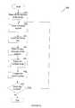
- FIG. 3is a flowchart describing the method for clock gating registers in the design of ICs according to one exemplary embodiment of the invention.
- a method for optimization of clock gating in integrated circuit (IC) designis very useful in reducing the electrical power consumed by an IC.
- the present inventionprovides a general method for identifying registers that are candidates for clock gating. Furthermore, the invention determines which of the candidate registers to clock gate in order to achieve optimal power and IC area savings. The determination is based on switching activity of the candidate registers.
- method 400further identifies registers without a feedback loop as candidates for clock gating.
- registersmay be registers with common enable signals and clock inputs present across various units in the IC design.
- registers with fanout of higher than a prespecified thresholdare also identified as possible candidates for clock gating, since such registers tend to impact large portions of the design.
- the thresholdin this case is a user specified parameter.
- logic blocks that include registers and multiplexers connected with a feedback loopare also identified as clock gated.
- step 510the gating list is received and, at step 520 , a single register from the list is selected.
- the logical condition that results in data being held by the selected registeri.e., the logical condition that defines the output function of the selected register is determined.
- the gating conditions for the selected registerare determined. This is performed by identifying control signals that create a simple feedback loop without any combinational logic components in the path, except for gates whose functions become equivalent to simple buffers.
- the candidate listis received.
- the switching activity of the registeris computed.
- the activitycan be computed using statistical algorithms, simulation-based algorithms, or a combination thereof.
- the switching activity of combinatorial and sequential elementsis estimated based on the activity of the inputs of the element. That is, given input switching rates, the probability of each gate switching at any particular time point is computed. These probabilities are then summed up over all the gates to obtain the expected switching activity in the entire circuit over all the time points corresponding to a clock cycle.
- a cumulative effectiveness reportmay be generated.
- registers in the gating listmay be sorted according to their gating effectiveness and registers having a gating effectiveness value below a predefined threshold are removed from the gating list.
- Cumulative effectiveness for a register groupis equal to the GE of the group plus the cumulative effectiveness of its previous register group in the sorted list of gating effectiveness.
Landscapes
- Engineering & Computer Science (AREA)
- Computer Hardware Design (AREA)
- Physics & Mathematics (AREA)
- Theoretical Computer Science (AREA)
- Evolutionary Computation (AREA)
- Geometry (AREA)
- General Engineering & Computer Science (AREA)
- General Physics & Mathematics (AREA)
- Design And Manufacture Of Integrated Circuits (AREA)
Abstract
Description
- This application is a continuation-in-part of U.S. patent application Ser. No. 10/631,755 filed on Aug. 1, 2003, the content of which is incorporated herein by reference in its entirety.
- The present invention relates generally to the design of ICs using a gated clock design technique, and more particularly to the low power IC design.
- In recent years, the size of integrated circuits (ICs) has dramatically increased in both size and number of transistors, resulting in higher power consumption. In typical IC designs, the clock distribution network, i.e., the clock tree, can consume from twenty to fifty percent of an IC's total active power. One important technique for reducing power consumption in IC designs is to reduce the power of an IC's clock distribution tree by gating portions of the IC that do not need to be clocked under certain conditions.
- This process, known as “clock gating”, disables the clocks fed to logic blocks of the IC when the logic blocks are not currently enabled or otherwise in active use. Power consumption due to the clocking of logic blocks that are not directly involved with the current operation of the IC is thereby minimized.
- Reference is now made to
FIG. 1 that shows apartial logic circuit 100 that has not been clock gated.Circuit 100 includes a synchronous load-enableregister 110 and a multiplexer (MUX)120 implementing the load enabling. The clock input port provides the clock signal “CLK” which clocks register110 every cycle. The enable port provides an enable signal “EN” that enables MUX120, thereby allows data propagation fromlogic 130 to register110. Obviously, there is no need to clock register110 on every cycle, since the data at the input ofregister 110 does not change every clock cycle. - Reference is now made to
FIG. 2 that shows apartial logic circuit 200 to which a clock gating technique is applied. Incircuit 200, anAND gate 210 is used as the gating circuit. The clock and the enable ports are connected to ANDgate 210 as its inputs. When the enable signal is set to a logic value ‘1’, data is input to register110 synchronously with the clock signal “CLK”. On the other hand, when the enable signal is set to a logic value ‘0’, data is not input to register110 irrespective of the clock signal. Accordingly, when there is no need for loading data to register110, unnecessary power consumption can be avoided by outputting the enable signals of a logic zero synchronously with the clock signal. TheAND gate 210 controls the load enable signal ofregister 110 thus MUX120 is eliminated from the circuit. - The clock gating technique is well known in the art as an effective technique for reducing the dynamic power of a system. In fact, the amount of dynamic power reduction depends on the number of registers that are gated and the percentage of time that the gated clock (i.e., the output of AND gate210) is enabled. However, gating all registers in the design increases the size of the IC. As a result, traditional approaches gate all the registers having size greater than a predefined threshold. Alternatively, registers to be clock gated are manually selected. These approaches are not optimal, in terms of power and area cost, as most of the savings can be achieved using only few clock gating structures.
- It would be therefore advantageous to provide a more efficient approach for selecting registers that are candidates for clock gating implementation.
FIG. 1 is a partial logic circuit which has not been clock gated (prior art).FIG. 2 is a partial logic circuit to which the clock gating technique is applied.FIG. 3 is a flowchart describing the method for clock gating registers in the design of ICs according to one exemplary embodiment of the invention.FIG. 4 is a flowchart describing the method for identifying registers that are candidates for clock gating.FIG. 5 is a flowchart describing the process for generating clock gated circuitsFIG. 6 is a resultant logic circuit which is clock gated in accordance with the disclosed inventionFIG. 7 is a flowchart describing the method for determining the optimal registers to be clock gated in accordance with an exemplary embodiment of the present invention- A method for optimization of clock gating in integrated circuit (IC) design. Clock gating techniques are very useful in reducing the electrical power consumed by an IC. The present invention provides a general method for identifying registers that are candidates for clock gating. Furthermore, the invention determines which of the candidate registers to clock gate in order to achieve optimal power and IC area savings. The determination is based on switching activity of the candidate registers.
- Reference is now made to
FIG. 3 which shows aflowchart 300 describing the method, according to one exemplary embodiment of the invention, for clock gating registers in the design of ICs. Although the examples presented herein include only a limited number of gates, this is merely for the purpose of simple explanations of the various exemplary embodiments of the invention. The examples should not be viewed as limiting the scope of the disclosed invention and it is specifically noted that the methods disclosed herein are operative with respect to designs of ICs that include a large number of logic gates and a large number of time domains. - At
step 310, registers with a feedback loop as well as other registers that are likely candidates for clock gating, encountered in a given design, are identified. All the registers that are candidates for clock gating are saved in a temporary list (also referred to as the “candidates list”). Referring toFIG. 4 , a detailed description of one implementation ofstep 310 is provided. According to an exemplary embodiment of the invention, the candidate registers are detected using a synthesized netlist produced by an IC synthesis tool. Synthesis tools produce gate level netlists based on the register transfer level (RTL) statements. - Netlists generally include logical gates such as AND, NAND, NOR, OR, XOR, NXOR, and the likes. One such synthesis tool is described in the co-pending US patent application entitled, “An Apparatus and Method for Handling of Multi-Level Circuit Design Data”, Ser. No. 10/118,242, assigned to common assignee and hereby incorporated by reference in its entirety. At
step 410, all the registers in the design are marked as candidates for clock gating. Atstep 420, a single marked register is selected. Atstep 430, there is created a list of nets connected to the register fanout (hereinafter “fanout list”) of the currently marked register. The fanout is the output terminal on a register or the net attached to an output terminal. - At
step 440, all the input data pins of the selected register are marked. Atstep 450, for each net in the fanout list, the method identifies a feedback loop connected between the net and the data input pins. The feedback loop should exclude combinational logic elements. Atstep 460 the currently examined register is unmarked and atstep 470, a check is performed to determine if there are more marked candidate registers to examine and, if there are, execution continues withstep 420; otherwise, execution is terminated. - In another exemplary embodiment of the invention, method400 further identifies registers without a feedback loop as candidates for clock gating. Such registers may be registers with common enable signals and clock inputs present across various units in the IC design. In addition, registers with fanout of higher than a prespecified threshold are also identified as possible candidates for clock gating, since such registers tend to impact large portions of the design. The threshold in this case is a user specified parameter. Furthermore, logic blocks that include registers and multiplexers connected with a feedback loop are also identified as clock gated.
- Another exemplary embodiment of the invention uses some heuristics in method400 to eliminate certain feedback paths identified as candidates for clock gating. For example, if the feedback path contains only an inverter, then it is considered to be a derived clock and eliminated as a candidate for clock gating. As another example, if the feedback path contains an incrementor (i.e., a basic binary adder), decrementor, or any arithmetic operations with one of the operands as constants, then it is eliminated as a candidate for clock gating.
- Referring back to
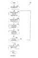
FIG. 3 , where, atstep 320, it is determined whether the candidates list is empty. If the list is empty, then execution ends. Otherwise, the execution continues withstep 330. Atstep 330, from the candidate registers the optimal registers to be clock gated are determined. The determination is based on the activity of a clock signal, probability of an enable signal, and the size of each candidate register. The result ofstep 330 is a list of registers to be gated (also referred to as the “gating list”). A more detailed description of one implementation ofstep 330 is provided below with reference toFIG. 7 . Atstep 340 another check is made to determine if the gating list is empty, and of so execution terminates; otherwise execution continues with350. Atstep 350 the clock gated circuits are generated by gating the registers in the gating list. - Reference is now made to
FIG. 5 where the execution ofstep 350 is shown greater detail. Atstep 510 the gating list is received and, atstep 520, a single register from the list is selected. At530, the logical condition that results in data being held by the selected register, i.e., the logical condition that defines the output function of the selected register is determined. Atstep 540, the gating conditions for the selected register are determined. This is performed by identifying control signals that create a simple feedback loop without any combinational logic components in the path, except for gates whose functions become equivalent to simple buffers. - At
step 550, the hold expressions are determined. Hold expressions are the remaining logical expressions being fed into the data input of the selected register, after the register output function has been evaluated with respect to the clock gating conditions. Atstep 560, a check is performed to determine if all the registers in the gating list were examined. If so, execution continues atstep 570; otherwise, execution continues atstep 520. Atstep 570, the clock gated circuits are formed by gating the registers. The gating circuits are generated using the output functions, gating conditions, and hold expressions. In any design, gating the registers results in the formation of a number of gated clock domains. FIG. 6 shows anexemplary circuit 600 that was gated using the techniques described herein. Specifically, the combinatorial logic (CL)640 is generated using the computed output functions, gating conditions, and hold expressions and inserted to the design. TheCL 640 is connected to an ANDgate 620 which is also added tocircuit 600.FIG. 7 shows an exemplary andnon-limiting flowchart 530 describing the method for determining the optimal registers to be clock gated in accordance with an exemplary embodiment of the present invention. The clock gating candidates are selected based on the switching activity information to ensure optimal power and area saving. Specifically, the switching activity information includes the activity of the clock signal, the probability of the enable signal, and the size of the candidate register. The clock activity and its frequency have a direct relationship with the power consumed by the registers. The probability of the enable signal identifies registers that are always enabled, and thus gating such registers is ineffective. The size of the candidate register determines how many registers can be connected to the same clock gating structure.- At
step 710 the candidate list is received. Atstep 720, for each register in the candidate list, the switching activity of the register is computed. The activity can be computed using statistical algorithms, simulation-based algorithms, or a combination thereof. The switching activity of combinatorial and sequential elements is estimated based on the activity of the inputs of the element. That is, given input switching rates, the probability of each gate switching at any particular time point is computed. These probabilities are then summed up over all the gates to obtain the expected switching activity in the entire circuit over all the time points corresponding to a clock cycle. Algorithms for computing the switching activity of combinatorial elements (e.g., AND gates, NAND gates, NOR gates, OR gates, XOR gates, NOT gates, and the like) are well known in the art. The switching activity of sequential elements is computed using various models. For example, the probability of an output Q of a simple flip-flop can be computed using the equation:
p—Q=(p—Q_old*(100−(t—CP/2))+(p—D*(t—CP/2)))/100;
where, p_Q_old is a predefined value (e.g., 50) t_CP is the activity of the clock signal and p_D is the input probability. P_Q_old is assumed to be 50, since it is equiprobable that the flop could have contained either ‘0’ or ‘1’ before the state change. Equal weights are given to the previous state of the flop and the new state of the flop. - The activity of the output Q (t_Q) is computed as follows:
if
(t_CP<=t_D)
t_Q=t_CP;
else
t—Q=(p—E*t—D)/100;
where, t_D is the activity of the input and p_E is the probability of the enable signal if the clock is gated. If the flip-flop is not an enabled flip-flop, p_E is set to 100. If the flip-flop is an enabled flip-flop, a state change occurs only if the enable is equal to ‘1’. Thus p_E, i.e., the probability of Enable being 1 is taken into consideration. - As another example, the probability (p_Q) and the activity (t_Q) of an output Q of an enabled latch are computed as follows:
p_Q=p_D;
t—Q=((t—D*p—E)/100) - Using the statistical algorithms, the switching activity of a design can be quickly calculated, as time-consuming simulations are not required.
- In some cases the method uses simulation data for computing switching activity. Specifically, for all the nets that were simulated the switching activity can be generated based on the number of toggles from ‘0’ to ‘1’ and from ‘1’ to ‘0’ during simulation. The method can further use both statistical techniques and simulation data for generating the switching activity of the design. That is, for nets that simulation data is not available the activity is computed using the statistical algorithms.
- At S730, in a design with multiple clock domains, all the activity of the clock is normalized according to the clock with the highest activity. At S740, registers having a common clock (which is not gated) and an enable signal are grouped together and added, at S750, to the gating list. At S760, the gating effectiveness of each group of registers in the gating list is calculated. The gating effectiveness is a function of the size of group (i.e., number of registers in the group), activity of the common clock (or the net driving the clock), and probability of the common enable. In one exemplary embodiment the gating effectiveness (GE) is computed using the following is equation:
GE=Size of candidate*Activity of clock net*Probability of enable net - Based on the gating effectiveness of each groups a cumulative effectiveness report may be generated. At S770, registers in the gating list may be sorted according to their gating effectiveness and registers having a gating effectiveness value below a predefined threshold are removed from the gating list. Cumulative effectiveness for a register group is equal to the GE of the group plus the cumulative effectiveness of its previous register group in the sorted list of gating effectiveness.
Claims (38)
Priority Applications (1)
| Application Number | Priority Date | Filing Date | Title |
|---|---|---|---|
| US11/419,624US7546559B2 (en) | 2003-08-01 | 2006-05-22 | Method of optimization of clock gating in integrated circuit designs |
Applications Claiming Priority (2)
| Application Number | Priority Date | Filing Date | Title |
|---|---|---|---|
| US10/631,755US7076748B2 (en) | 2003-08-01 | 2003-08-01 | Identification and implementation of clock gating in the design of integrated circuits |
| US11/419,624US7546559B2 (en) | 2003-08-01 | 2006-05-22 | Method of optimization of clock gating in integrated circuit designs |
Related Parent Applications (1)
| Application Number | Title | Priority Date | Filing Date |
|---|---|---|---|
| US10/631,755Continuation-In-PartUS7076748B2 (en) | 2003-08-01 | 2003-08-01 | Identification and implementation of clock gating in the design of integrated circuits |
Publications (2)
| Publication Number | Publication Date |
|---|---|
| US20060248487A1true US20060248487A1 (en) | 2006-11-02 |
| US7546559B2 US7546559B2 (en) | 2009-06-09 |
Family
ID=46324525
Family Applications (1)
| Application Number | Title | Priority Date | Filing Date |
|---|---|---|---|
| US11/419,624Expired - LifetimeUS7546559B2 (en) | 2003-08-01 | 2006-05-22 | Method of optimization of clock gating in integrated circuit designs |
Country Status (1)
| Country | Link |
|---|---|
| US (1) | US7546559B2 (en) |
Cited By (12)
| Publication number | Priority date | Publication date | Assignee | Title |
|---|---|---|---|---|
| US20080216024A1 (en)* | 2004-05-24 | 2008-09-04 | New Wei Lee | Method and Apparatus for Allocating Data Paths |
| US20080301593A1 (en)* | 2007-05-29 | 2008-12-04 | Magma Design Automation, Inc. | Method For Automatic Clock Gating To Save Power |
| US20080301604A1 (en)* | 2007-05-30 | 2008-12-04 | Alexander Itskovich | Apparatus for and method of estimating the quality of clock gating solutions for integrated circuit design |
| GB2456363A (en)* | 2008-01-08 | 2009-07-15 | Ibm | Methods and system for clock gating enhancement |
| US7884649B1 (en)* | 2009-02-27 | 2011-02-08 | Magma Design Automation, Inc. | Selection of optimal clock gating elements |
| US8898604B1 (en)* | 2013-07-16 | 2014-11-25 | International Business Machines Corporation | Algorithm to identify best Q-gating candidates and a Q-gating cell architecture to satiate the launch-off-shift (LOS) testing |
| US9077371B2 (en) | 2012-10-31 | 2015-07-07 | Qualcomm Incorporated | Methods and apparatus for a successive approximation register analog-to-digital converter |
| US9086458B2 (en) | 2013-08-28 | 2015-07-21 | International Business Machines Corporation | Q-gating cell architecture to satiate the launch-off-shift (LOS) testing and an algorithm to identify best Q-gating candidates |
| CN116090371A (en)* | 2022-12-15 | 2023-05-09 | 上海华大九天信息科技有限公司 | A Method of Inserting Clock Gating in Integrated Circuit Design |
| CN116895325A (en)* | 2023-06-21 | 2023-10-17 | 合芯科技有限公司 | ICG classification method, test method and classification device for digital array registers |
| CN118643775A (en)* | 2024-08-14 | 2024-09-13 | 山东启芯软件科技有限公司 | Integrated circuit design power consumption optimization method and device with multi-level clock gating inserted |
| US12241931B1 (en)* | 2022-01-12 | 2025-03-04 | Marvell Asia Pte Ltd | Method and apparatus for capture clock control to minimize toggling during testing |
Families Citing this family (5)
| Publication number | Priority date | Publication date | Assignee | Title |
|---|---|---|---|---|
| WO2011107828A1 (en) | 2010-03-03 | 2011-09-09 | Freescale Semiconductor, Inc. | Integrated circuit device comprising clock gating circuitry, electronic device and method for dynamically configuring clock gating |
| US8656326B1 (en) | 2013-02-13 | 2014-02-18 | Atrenta, Inc. | Sequential clock gating using net activity and XOR technique on semiconductor designs including already gated pipeline design |
| WO2016203491A2 (en)* | 2015-06-16 | 2016-12-22 | Gyan Prakash | Asynchronous clock gating circuit |
| US10141916B2 (en) | 2015-09-01 | 2018-11-27 | Samsung Electronics Co., Ltd. | High-speed flip-flop semiconductor device |
| KR102611888B1 (en) | 2016-11-07 | 2023-12-11 | 삼성전자주식회사 | Layout method for semiconductor device based on swiching activity and manufacturing |
Citations (17)
| Publication number | Priority date | Publication date | Assignee | Title |
|---|---|---|---|---|
| US5585745A (en)* | 1995-02-14 | 1996-12-17 | Vlsi Technology, Inc. | Method and apparatus for reducing power consumption in digital electronic circuits |
| US5623418A (en)* | 1990-04-06 | 1997-04-22 | Lsi Logic Corporation | System and method for creating and validating structural description of electronic system |
| US5740087A (en)* | 1996-05-31 | 1998-04-14 | Hewlett-Packard Company | Apparatus and method for regulating power consumption in a digital system |
| US5980092A (en)* | 1996-11-19 | 1999-11-09 | Unisys Corporation | Method and apparatus for optimizing a gated clock structure using a standard optimization tool |
| US6049883A (en)* | 1998-04-01 | 2000-04-11 | Tjandrasuwita; Ignatius B. | Data path clock skew management in a dynamic power management environment |
| US6167561A (en)* | 1998-06-08 | 2000-12-26 | Synopsis, Inc. | Method and apparatus for entry of timing constraints |
| US6204695B1 (en)* | 1999-06-18 | 2001-03-20 | Xilinx, Inc. | Clock-gating circuit for reducing power consumption |
| US6240542B1 (en)* | 1998-07-14 | 2001-05-29 | Lsi Logic Corporation | Poly routing for chip interconnects with minimal impact on chip performance |
| US6272667B1 (en)* | 1997-10-09 | 2001-08-07 | Kabushiki Kaisha Toshiba | Method and apparatus for clock gated logic circuits to reduce electric power consumption |
| US6324679B1 (en)* | 1997-06-03 | 2001-11-27 | Nec Usa, Inc. | Register transfer level power optimization with emphasis on glitch analysis and reduction |
| US6429698B1 (en)* | 2000-05-02 | 2002-08-06 | Xilinx, Inc. | Clock multiplexer circuit with glitchless switching |
| US6434704B1 (en)* | 1999-08-16 | 2002-08-13 | International Business Machines Corporation | Methods for improving the efficiency of clock gating within low power clock trees |
| US6567962B2 (en)* | 2000-11-30 | 2003-05-20 | International Business Machines Corporation | Method, apparatus, and program for multiple clock domain partitioning through retiming |
| US20030140318A1 (en)* | 1999-09-14 | 2003-07-24 | Kabushiki Kaisha Toshiba | Computer aided design system and computer-readable medium storing a program for designing clock gated logic circuits and gated clock circuit |
| US20040123258A1 (en)* | 2002-12-20 | 2004-06-24 | Quickturn Design Systems, Inc. | Logic multiprocessor for FPGA implementation |
| US20040225978A1 (en)* | 2003-05-09 | 2004-11-11 | Yong Fan | Automatic clock gating insertion in an IC design |
| US20040250227A1 (en)* | 2003-06-09 | 2004-12-09 | Kuoching Lin | Representing device layout using tree structure |
- 2006
- 2006-05-22USUS11/419,624patent/US7546559B2/ennot_activeExpired - Lifetime
Patent Citations (19)
| Publication number | Priority date | Publication date | Assignee | Title |
|---|---|---|---|---|
| US5623418A (en)* | 1990-04-06 | 1997-04-22 | Lsi Logic Corporation | System and method for creating and validating structural description of electronic system |
| US5585745A (en)* | 1995-02-14 | 1996-12-17 | Vlsi Technology, Inc. | Method and apparatus for reducing power consumption in digital electronic circuits |
| US5740087A (en)* | 1996-05-31 | 1998-04-14 | Hewlett-Packard Company | Apparatus and method for regulating power consumption in a digital system |
| US5980092A (en)* | 1996-11-19 | 1999-11-09 | Unisys Corporation | Method and apparatus for optimizing a gated clock structure using a standard optimization tool |
| US6324679B1 (en)* | 1997-06-03 | 2001-11-27 | Nec Usa, Inc. | Register transfer level power optimization with emphasis on glitch analysis and reduction |
| US6272667B1 (en)* | 1997-10-09 | 2001-08-07 | Kabushiki Kaisha Toshiba | Method and apparatus for clock gated logic circuits to reduce electric power consumption |
| US6049883A (en)* | 1998-04-01 | 2000-04-11 | Tjandrasuwita; Ignatius B. | Data path clock skew management in a dynamic power management environment |
| US6167561A (en)* | 1998-06-08 | 2000-12-26 | Synopsis, Inc. | Method and apparatus for entry of timing constraints |
| US6240542B1 (en)* | 1998-07-14 | 2001-05-29 | Lsi Logic Corporation | Poly routing for chip interconnects with minimal impact on chip performance |
| US6204695B1 (en)* | 1999-06-18 | 2001-03-20 | Xilinx, Inc. | Clock-gating circuit for reducing power consumption |
| US6434704B1 (en)* | 1999-08-16 | 2002-08-13 | International Business Machines Corporation | Methods for improving the efficiency of clock gating within low power clock trees |
| US20030140318A1 (en)* | 1999-09-14 | 2003-07-24 | Kabushiki Kaisha Toshiba | Computer aided design system and computer-readable medium storing a program for designing clock gated logic circuits and gated clock circuit |
| US7062725B2 (en)* | 1999-09-14 | 2006-06-13 | Kabushiki Kaisha Toshiba | Computer aided design system and computer-readable medium storing a program for designing clock gated logic circuits and gated clock circuit |
| US6429698B1 (en)* | 2000-05-02 | 2002-08-06 | Xilinx, Inc. | Clock multiplexer circuit with glitchless switching |
| US6567962B2 (en)* | 2000-11-30 | 2003-05-20 | International Business Machines Corporation | Method, apparatus, and program for multiple clock domain partitioning through retiming |
| US20040123258A1 (en)* | 2002-12-20 | 2004-06-24 | Quickturn Design Systems, Inc. | Logic multiprocessor for FPGA implementation |
| US20040225978A1 (en)* | 2003-05-09 | 2004-11-11 | Yong Fan | Automatic clock gating insertion in an IC design |
| US7080334B2 (en)* | 2003-05-09 | 2006-07-18 | Incentia Design Systems Corp. | Automatic clock gating insertion in an IC design |
| US20040250227A1 (en)* | 2003-06-09 | 2004-12-09 | Kuoching Lin | Representing device layout using tree structure |
Cited By (16)
| Publication number | Priority date | Publication date | Assignee | Title |
|---|---|---|---|---|
| US20080216024A1 (en)* | 2004-05-24 | 2008-09-04 | New Wei Lee | Method and Apparatus for Allocating Data Paths |
| US7689940B2 (en)* | 2004-05-24 | 2010-03-30 | Panasonic Corporation | Method and apparatus for allocating data paths |
| US7930673B2 (en) | 2007-05-29 | 2011-04-19 | Magma Design Automation, Inc. | Method for automatic clock gating to save power |
| US20080301593A1 (en)* | 2007-05-29 | 2008-12-04 | Magma Design Automation, Inc. | Method For Automatic Clock Gating To Save Power |
| WO2008150889A1 (en)* | 2007-05-29 | 2008-12-11 | Magma Design Automation, Inc. | A method for automatic clock gating to save power |
| US8434047B1 (en) | 2007-05-29 | 2013-04-30 | Synopsys, Inc. | Multi-level clock gating circuitry transformation |
| US20080301604A1 (en)* | 2007-05-30 | 2008-12-04 | Alexander Itskovich | Apparatus for and method of estimating the quality of clock gating solutions for integrated circuit design |
| GB2456363A (en)* | 2008-01-08 | 2009-07-15 | Ibm | Methods and system for clock gating enhancement |
| US7884649B1 (en)* | 2009-02-27 | 2011-02-08 | Magma Design Automation, Inc. | Selection of optimal clock gating elements |
| US9077371B2 (en) | 2012-10-31 | 2015-07-07 | Qualcomm Incorporated | Methods and apparatus for a successive approximation register analog-to-digital converter |
| US8898604B1 (en)* | 2013-07-16 | 2014-11-25 | International Business Machines Corporation | Algorithm to identify best Q-gating candidates and a Q-gating cell architecture to satiate the launch-off-shift (LOS) testing |
| US9086458B2 (en) | 2013-08-28 | 2015-07-21 | International Business Machines Corporation | Q-gating cell architecture to satiate the launch-off-shift (LOS) testing and an algorithm to identify best Q-gating candidates |
| US12241931B1 (en)* | 2022-01-12 | 2025-03-04 | Marvell Asia Pte Ltd | Method and apparatus for capture clock control to minimize toggling during testing |
| CN116090371A (en)* | 2022-12-15 | 2023-05-09 | 上海华大九天信息科技有限公司 | A Method of Inserting Clock Gating in Integrated Circuit Design |
| CN116895325A (en)* | 2023-06-21 | 2023-10-17 | 合芯科技有限公司 | ICG classification method, test method and classification device for digital array registers |
| CN118643775A (en)* | 2024-08-14 | 2024-09-13 | 山东启芯软件科技有限公司 | Integrated circuit design power consumption optimization method and device with multi-level clock gating inserted |
Also Published As
| Publication number | Publication date |
|---|---|
| US7546559B2 (en) | 2009-06-09 |
Similar Documents
| Publication | Publication Date | Title |
|---|---|---|
| US7546559B2 (en) | Method of optimization of clock gating in integrated circuit designs | |
| US7076748B2 (en) | Identification and implementation of clock gating in the design of integrated circuits | |
| US6345379B1 (en) | Method and apparatus for estimating internal power consumption of an electronic circuit represented as netlist | |
| JP3331968B2 (en) | Register transfer level power consumption optimization circuit, method and recording medium with emphasis on glitch analysis and reduction | |
| US5838947A (en) | Modeling, characterization and simulation of integrated circuit power behavior | |
| US6434704B1 (en) | Methods for improving the efficiency of clock gating within low power clock trees | |
| US6397170B1 (en) | Simulation based power optimization | |
| US8266569B2 (en) | Identification of critical enables using MEA and WAA metrics | |
| US6195786B1 (en) | Constrained register sharing technique for low power VLSI design | |
| US7080334B2 (en) | Automatic clock gating insertion in an IC design | |
| US20070011643A1 (en) | Optimized mapping of an integrated circuit design to multiple cell libraries during a single synthesis pass | |
| Youssef et al. | Timing constraints for correct performance | |
| US20080201671A1 (en) | Method for generating timing exceptions | |
| Gupta et al. | Analytical models for RTL power estimation of combinational and sequential circuits | |
| Rohfleisch et al. | Reducing power dissipation after technology mapping by structural transformations | |
| US7509606B2 (en) | Method for optimizing power in a very large scale integration (VLSI) design by detecting clock gating opportunities | |
| US8776003B2 (en) | System and method for employing side transition times from signoff-quality timing analysis information to reduce leakage power in an electronic circuit and an electronic design automation tool incorporating the same | |
| US7941679B2 (en) | Method for computing power savings and determining the preferred clock gating circuit of an integrated circuit design | |
| US7007247B1 (en) | Method and mechanism for RTL power optimization | |
| Mukheijee et al. | Clock and power gating with timing closure | |
| Oelmann et al. | Automatic FSM Synthesis for Low‐power Mixed Synchronous/Asynchronous Implementation | |
| Dey et al. | Controller-based power management for control-flow intensive designs | |
| Wang et al. | Power reduction and power-delay trade-offs using logic transformations | |
| Paik et al. | Clock gating synthesis of pulsed-latch circuits | |
| US12373625B1 (en) | Timing domain based modeling of switching probability and signal correlation |
Legal Events
| Date | Code | Title | Description |
|---|---|---|---|
| AS | Assignment | Owner name:ATRENTA, INC., CALIFORNIA Free format text:ASSIGNMENT OF ASSIGNORS INTEREST;ASSIGNORS:KAPOOR, BHANU;BAGCHI, DEBABRATA;SHARMA, NITIN;REEL/FRAME:017904/0883;SIGNING DATES FROM 20060525 TO 20060526 | |
| AS | Assignment | Owner name:HERCULES TECHNOLOGY GROWTH CAPITAL, INC., CALIFORN Free format text:SECURITY AGREEMENT;ASSIGNOR:ATRENTA, INC.;REEL/FRAME:021222/0668 Effective date:20051229 Owner name:HERCULES TECHNOLOGY GROWTH CAPITAL, INC.,CALIFORNI Free format text:SECURITY AGREEMENT;ASSIGNOR:ATRENTA, INC.;REEL/FRAME:021222/0668 Effective date:20051229 | |
| AS | Assignment | Owner name:SILICON VALLEY BANK, CALIFORNIA Free format text:SECURITY AGREEMENT;ASSIGNOR:ATRENTA INC.;REEL/FRAME:022542/0570 Effective date:20090414 Owner name:SILICON VALLEY BANK,CALIFORNIA Free format text:SECURITY AGREEMENT;ASSIGNOR:ATRENTA INC.;REEL/FRAME:022542/0570 Effective date:20090414 | |
| AS | Assignment | Owner name:ATRENTA INC., CALIFORNIA Free format text:RELEASE BY SECURED PARTY;ASSIGNOR:HERCULES TECHNOLOGY GROWTH CAPITAL, INC.;REEL/FRAME:022552/0639 Effective date:20090414 | |
| STCF | Information on status: patent grant | Free format text:PATENTED CASE | |
| FPAY | Fee payment | Year of fee payment:4 | |
| AS | Assignment | Owner name:ATRENTA INC., CALIFORNIA Free format text:RELEASE BY SECURED PARTY;ASSIGNOR:SILICON VALLEY BANK;REEL/FRAME:036584/0644 Effective date:20150825 | |
| AS | Assignment | Owner name:SYNOPSYS, INC., CALIFORNIA Free format text:ASSIGNMENT OF ASSIGNORS INTEREST;ASSIGNOR:ATRENTA INC.;REEL/FRAME:036687/0290 Effective date:20150922 | |
| FEPP | Fee payment procedure | Free format text:PAT HOLDER NO LONGER CLAIMS SMALL ENTITY STATUS, ENTITY STATUS SET TO UNDISCOUNTED (ORIGINAL EVENT CODE: STOL); ENTITY STATUS OF PATENT OWNER: LARGE ENTITY | |
| FPAY | Fee payment | Year of fee payment:8 | |
| MAFP | Maintenance fee payment | Free format text:PAYMENT OF MAINTENANCE FEE, 12TH YEAR, LARGE ENTITY (ORIGINAL EVENT CODE: M1553); ENTITY STATUS OF PATENT OWNER: LARGE ENTITY Year of fee payment:12 |