US20060244105A1 - Strained semiconductor by full wafer bonding - Google Patents
Strained semiconductor by full wafer bondingDownload PDFInfo
- Publication number
- US20060244105A1 US20060244105A1US11/475,798US47579806AUS2006244105A1US 20060244105 A1US20060244105 A1US 20060244105A1US 47579806 AUS47579806 AUS 47579806AUS 2006244105 A1US2006244105 A1US 2006244105A1
- Authority
- US
- United States
- Prior art keywords
- wafer
- substrate
- semiconductor layer
- various embodiments
- strain
- Prior art date
- Legal status (The legal status is an assumption and is not a legal conclusion. Google has not performed a legal analysis and makes no representation as to the accuracy of the status listed.)
- Granted
Links
Images


Classifications
- H—ELECTRICITY
- H01—ELECTRIC ELEMENTS
- H01L—SEMICONDUCTOR DEVICES NOT COVERED BY CLASS H10
- H01L21/00—Processes or apparatus adapted for the manufacture or treatment of semiconductor or solid state devices or of parts thereof
- H01L21/70—Manufacture or treatment of devices consisting of a plurality of solid state components formed in or on a common substrate or of parts thereof; Manufacture of integrated circuit devices or of parts thereof
- H01L21/71—Manufacture of specific parts of devices defined in group H01L21/70
- H01L21/76—Making of isolation regions between components
- H01L21/762—Dielectric regions, e.g. EPIC dielectric isolation, LOCOS; Trench refilling techniques, SOI technology, use of channel stoppers
- H01L21/7624—Dielectric regions, e.g. EPIC dielectric isolation, LOCOS; Trench refilling techniques, SOI technology, use of channel stoppers using semiconductor on insulator [SOI] technology
- H01L21/76251—Dielectric regions, e.g. EPIC dielectric isolation, LOCOS; Trench refilling techniques, SOI technology, use of channel stoppers using semiconductor on insulator [SOI] technology using bonding techniques
- H01L21/76254—Dielectric regions, e.g. EPIC dielectric isolation, LOCOS; Trench refilling techniques, SOI technology, use of channel stoppers using semiconductor on insulator [SOI] technology using bonding techniques with separation/delamination along an ion implanted layer, e.g. Smart-cut, Unibond
Definitions
- This disclosurerelates generally to integrated circuits, and more particularly, to strained semiconductor structures.
- Strained silicon technologyenhances carrier mobility in both n-channel and p-channel devices, and thus improves device speed and performance.
- One technique for producing strained siliconinvolves growing silicon on relaxed silicon germanium (Si/SiGe) structures. There is a large mismatch in the cell structure between the Si and SiGe layers. This mismatch causes a pseudomorphic layer of Si on relaxed SiGe to be under a tensile strain that modifies the band structure and enhances carrier transport in the Si layer.
- the subband splittingis larger in strained Si because of the strain-induced band splitting in addition to that provided by quantum confinement.
- the ground level splitting (E 0 (d 4 ) ⁇ E 0 (d 2 )) in a MOS inversion layer at 1 MV/cm transverse fieldis ⁇ 120 meV for unstrained Si and 250 meV for strained Si.
- the increase in energy splittingreduces inter-valley scattering and enhances NMOSFET mobility, as demonstrated at low ( ⁇ 0.6 MV/cm) and higher ( ⁇ 1 MV/cm) vertical fields.
- the scaled transconductance (g m )is also improved due to the reduced density of states and enhanced non-equilibrium transport.
- One method for forming the Si/SiGe layerinvolves epitaxially growing the Si and SiGe layers using an ultra-high vacuum chemical vapor deposition (UHVCVD) process.
- UHVCVDultra-high vacuum chemical vapor deposition
- the UHVCVD processis a costly and complex process.
- the Ge contentis graded in steps to form a fully relaxed SiGe buffer layer before a thin ( ⁇ 20 nm) strained Si channel layer is grown.
- X-ray diffraction analysiscan be used to quantify the Ge content and strain relaxation in the SiGe layer.
- the strain state of the Si channel layercan be confirmed by Raman spectroscopy.
- One proposed back end approach for straining siliconapplies uniaxial strain to wafers/dies after the integrated circuit process is complete.
- the diesare thinned to membrane dimensions and then affixed to curved substrates to apply an in-plane, tensile strain after device manufacture.
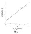
- FIG. 1illustrates the lattice constant of a Si 1-X Ge X substrate for different percentages (X) of Ge.
- FIG. 2illustrates the mobility enhancement for strained Si for different percentages (X) of Ge in a Si 1-X Ge X substrate.
- FIG. 3illustrates a relationship between elastic strain and semiconductor layer thicknesses.
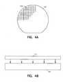
- FIGS. 4A-4Billustrate a wafer and a full wafer bonding process, respectively.
- FIGS. 5A-5Dillustrate a process for straining a semiconductor layer by performing a bond-cut process to bond the semiconductor layer to a flexed bow-shaped substrate, according to various embodiments of the present invention.
- FIGS. 6A-6Billustrate relaxed and flexed wafer positions, and a strain for a wafer in the flexed position.
- FIGS. 7A-7Billustrate a stress calculation for a bowed substrate wafer.
- FIG. 8illustrates a composite structure that includes a strained semiconductor membrane bonded to a flexible substrate, and further illustrates the composite structure being bonded to a thicker carrier substrate, according to various embodiments of the present invention.
- FIGS. 9A-9Billustrate a process for straining a semiconductor layer by performing a bond-cut process to a bowed substrate with voids, according to various embodiments of the present invention.
- FIG. 10A-10Fillustrate a process to form a wafer with a sphere-shaped empty space, according to various embodiments of the present invention.
- FIG. 11A-11Cillustrate a process to form a wafer with a pipe-shaped empty space, according to various embodiments of the present invention.
- FIGS. 12A-12Billustrate a process to form a wafer with a plate-shaped empty space, according to various embodiments of the present invention.
- FIG. 13A-13Eillustrate the formation of empty spheres from initial cylindrical holes in a wafer with the same radii and with varying length, according to various embodiments of the present invention.
- FIG. 14illustrates a wafer with a surface-transformation-formed stack of empty plates with a large filling factor or low density, according to various embodiments of the present invention.
- FIGS. 15A-15Cillustrate a process for straining a semiconductor layer by performing a bond-cut process to bond a relaxed bow-shaped semiconductor layer to and flatten the semiconductor layer against a rigid substrate, according to various embodiments of the present invention.
- FIGS. 16A-16Dillustrate a process for straining a semiconductor layer by bonding a concave surface of a crystalline wafer to a rigid substrate, according to various embodiments of the present invention.
- FIG. 17illustrates a process for forming a wafer with a strained semiconductor layer, according to various embodiments of the present invention.
- FIG. 18illustrates a process for forming a wafer with a strained semiconductor layer, according to various embodiments of the process illustrated in FIG. 17 .
- FIG. 19illustrates a process for forming a wafer with a strained semiconductor layer, according to various embodiments of the process illustrated in FIG. 17 .
- FIG. 20illustrates a process for forming a wafer with a strained semiconductor layer, according to various embodiments of the process illustrated in FIG. 17 .
- FIG. 21illustrates a process for forming a wafer with a strained semiconductor layer, according to various embodiments of the process illustrated in FIG. 17 .
- FIG. 22illustrates a process for forming a wafer with a strained semiconductor layer, according to various embodiments of the process illustrated in FIG. 17 .
- FIG. 23illustrates a transistor fabricated with a strained semiconductor membrane, according to various embodiments of the present invention.
- FIG. 24illustrates a simplified block diagram of a high-level organization of a memory device, according to various embodiments of the present invention.
- FIG. 25illustrates a simplified block diagram of a high-level organization of an electronic system according to various embodiments of the present invention.
- Both termsinclude doped and undoped semiconductors, epitaxial layers of a semiconductor on a supporting semiconductor or insulating material, combinations of such layers, as well as other such structures that are known in the art.
- the terms “horizontal” and “vertical”, as well as prepositions such as “on”, “over” and “under”are used in relation to the conventional plane or surface of a wafer or substrate, regardless of the orientation of the wafer or substrate. The following detailed description is, therefore, not to be taken in a limiting sense, and the scope of the present invention is defined only by the appended claims, along with the full scope of equivalents to which such claims are entitled.
- strained semiconductor layermechanically stretch a semiconductor layer during full wafer bonding to form a wafer with a strained semiconductor layer.
- the strained semiconductor layeris an ultra-thin silicon layer.
- a predetermined contouris formed in one of a semiconductor membrane and a substrate wafer.
- the semiconductor membraneis bonded to the substrate wafer and the predetermined contour is straightened to induce a predetermined strain in the semiconductor membrane.
- a substrate waferis flexed into a flexed position, a portion of the substrate wafer is bonded to a semiconductor layer when the substrate wafer is in the flexed position, and the substrate wafer is relaxed to induce a predetermined strain in the semiconductor layer.
- a central region of a substrate waferis flexed into a flexed position, a bond cut process is performed to form a silicon membrane from a crystalline sacrificial wafer and bond a peripheral region of the substrate wafer to a peripheral region of a silicon membrane when the substrate wafer is in the flexed position, and the substrate wafer is relaxed to induce a predetermined strain in the silicon membrane.
- a bond cut processis performed to form a silicon membrane from a crystalline sacrificial wafer and bond a peripheral region of the substrate wafer to a peripheral region of a silicon membrane when the substrate wafer is in the flexed position, and the substrate wafer is relaxed to induce a predetermined strain in the silicon membrane.
- aspects of the present inventionstrain a semiconductor layer, such as a crystalline silicon layer, by mechanical stretching of the semiconductor layer during full wafer bonding.
- the semiconductor layeris an ultra-thin semiconductor layer.
- Various embodimentsbond the ultra-thin semiconductor layer to a bowed flexible substrate during full wafer bonding.
- Various embodimentsbond a semiconductor layer with a bowed surface to a fixed wafer during a full wafer bonding.
- this disclosurediscusses a transistor that incorporates the strained semiconductor. Eighth, this disclosure discusses systems such as memory devices and computers. The headings and numbering used to organize the detailed description should not be used to limit the present invention, but rather are intended to assist the reader in navigating through this disclosure.
- This disclosurediscusses mechanically straining a wafer-sized semiconductor layer, i.e. straining a semiconductor layer at a wafer scale.
- siliconis mechanically strained to enhance carrier mobility.
- Other semiconductor materialcan be strained in accordance with the subject matter discussed herein. Research findings for Si/SiGe structures can be used to determine desirable mechanical strain.
- Sihas a lattice constant of 5.43095 ⁇
- Gehas a lattice constant of 5.64613 ⁇ .
- the lattice constant of SiGeis between the lattice constant of Si and the lattice constant of Ge, and depends on the percentage of Ge in the SiGe layer.
- FIG. 1illustrates the lattice constant of a Si 1-X Ge X substrate for different percentages (X) of Ge. As indicated by FIG. 1 , a Si 1-X Ge X substrate containing about 30% Ge (X ⁇ 0.3) has a lattice constant of about 5.50 ⁇ .
- FIG. 2illustrates the mobility enhancement for strained Si for different percentages (X) of Ge in a Si 1-X Ge X substrate.
- the mobility enhancementincreases as the percentage of Ge in the Si 1-X Ge X increases, and levels off to around 1.6 when the percentage of Ge is around 22% or larger.
- 22% Geprovides the Si 1-X Ge X substrate with a lattice constant (SiGe LC ) of around 5.485.
- SiGe LClattice constant
- FIG. 3illustrates a relationship between elastic strain and semiconductor layer thicknesses.
- the semiconductor yieldis plotted with respect to plastic deformation and defects in bulk samples.
- the illustrated valuesrepresent the relationship of thin SiGe layers on silicon.
- FIG. 3illustrates that thin layers of silicon or other semiconductor materials are more tolerant of strain than thick bulk samples.
- thin layers of SiGehave been fabricated on silicon because of the tolerance of the thin layers to strain.
- FIG. 3indicates that 1000 ⁇ thin semiconductor layers can be strained up to about 1%, that 100 ⁇ thin semiconductor layers can be strained up to about 2% and thinner semiconductor layers can be strained up to about 2.5%.
- the mobility enhancementlevels off when the strain reaches about 1%.
- a thin semiconductor layersuch as a silicon layer
- a strain greater than 0.5%it is desirable to strain a thin semiconductor wafer, such as an ultra-thin silicon wafer with a thickness within a range of approximately 300 ⁇ to 1000 ⁇ , with a strain within a range of approximately 0.75% to approximately 1.5% where the mobility enhancement levels off. It is also desirable to reduce unnecessary strain and provide a margin for error without unduly affecting the mobility enhancement.
- a thin semiconductor layersuch as a thin silicon layer, with a strain in the range of approximately 1% to approximately 1.2%.
- Ultra-thin waferssuch as single crystalline silicon wafers, have a thickness below approximately 200 microns, which is near the limit of known mechanical thinning techniques. Virginia Semiconductor, Inc. has produced these wafers with a thickness down to about 2 microns with diameters of up to 4 inches. Doping concentrations and profiles for these wafers are comparable to normal thickness wafers, and the Total Thickness Variation (TTV) is generally less than one micron. Bond-quality, ultra-thin wafers are double side polished and have micro-roughness comparable to prime grade, normal thickness wafers. Ultra-thin wafers that have a thickness of approximately 100 microns or more are mechanically similar to normal wafers and can be processed using standard techniques.
- the waferexhibits greater flexibility to the point, at about 20 microns thick, that the wafer can be deformed into a tube, with the wafer contacted flat with the opposite edge.
- ultra-thin wafersbecome transparent to visible light. The increased flexibility allows ultra-thin wafers to bond to surfaces with roughness orders of magnitude greater than the limit for bonding normal thicknesses.
- the bond cut techniqueimplants ions such as hydrogen, bonds two wafer surfaces together, and separates the two bonded wafers along the region of hydrogen implantation.
- the literatureindicates that memory structures have been inverted and stacked capacitors have been buried by wafer bonding.
- Various techniquessuch as grinding, polishing, chemical etch, chemical etch with etch stops, and/or plasma assisted chemical etch, can be used to further thin the top wafer to a thickness on the order of a micron after the wafers are bonded.
- oxide or siliconsilicon has been bonded on other materials such as sapphire wafers.
- the ultra-thin semiconductor filmis produced by a hydrogen implantation into a sacrificial wafer leaving a single crystalline 300 ⁇ to 1000 ⁇ surface layer which will separate from the carrier wafer when the film is bonded face down on the device wafer.
- the bonded layeris polished by chemical and/or mechanical means to make the surface smoother leaving an ultra-thin strained film on the order of 300 ⁇ to 1000 ⁇ thick.
- FIGS. 4A-4Billustrate a wafer and a full wafer bonding process, respectively.
- Various techniques to produce strained semiconductorinvolve a full wafer bonding technique.
- Various embodimentsproduce strained silicon layers on silicon, glass, quartz, silicon oxycarbide and other glass substrates.
- FIG. 4Aillustrates a wafer 401 .
- a common wafer sizeis 8 inches in diameter. However, wafers are capable of being fabricated in other sizes. The present invention is not limited to wafers of a particular size.
- a number of diescan be formed on a wafer.
- a die 402is an individual pattern, typically rectangular, on a substrate that contains circuitry to perform a specific function.
- a semiconductor wafertypically contains a repeated pattern of such dies containing the same functionality.
- a dieis typically packaged in a protective casing (not shown) with leads extending therefrom (not shown) providing access to the circuitry of the die for unilateral or bilateral communication and control.
- FIG. 4Bgenerally illustrates full wafer bonding process.
- a wafer-sized membrane 403is bonded to a wafer substrate 404 such that the substrate wafer, or at least as portion of the substrate wafer, is covered by the membrane.
- the wafer-sized membraneneed not be exactly the same size as the wafer.
- the term “wafer-sized”reflects that the bonding of the membrane to the wafer occurs on a wafer scale.
- the wafer substrate 404generally corresponds to the wafer 401 illustrated in FIG. 4A without dies.
- the circuitryis formed in the bonded membrane after the full wafer bonding process.
- Various techniques and mechanismscan be used to perform a full wafer bonding process.
- FIGS. 5A-5Dillustrate a process for straining a semiconductor layer by performing a bond-cut process to bond the semiconductor layer to a flexed bow-shaped substrate, according to various embodiments of the present invention.
- the bond cut processinvolves bonding together two substrates, or wafers, and breaking off a section (i.e. the membrane) of at least one of the two substrate after the substrates have been bonded together.
- the substrateis also referred to herein in various embodiments as a flexible wafer or substrate wafer.
- the membraneis broken off of a second wafer or sacrificial wafer.
- FIG. 5Aillustrates a sacrificial semiconductor wafer 505
- FIG. 5Billustrates a substrate wafer 504
- the substrate wafer 504includes one of the following materials: silicon; germanium; silicon-germanium; gallium arsenide; indium phosphide; and other semiconductor materials.
- the substrate wafer 504includes glass, quartz, silicon oxycarbide, and other glass substrates. This list of materials is not intended to be an all-inclusive list.
- the sacrificial waferincludes various semiconductor material including but not limited to silicon, germanium, silicon-germanium, gallium arsenide, indium phosphide.
- the sacrificial wafer 505can include other semiconductor materials.
- the sacrificial wafer 505is a single crystal wafer.
- the bond-cut techniqueconditions the sacrificial wafer 505 by implanting ions 506 into a surface 507 .
- the ionsare implanted along a plane, represented in FIG. 5A as a dotted line 508 , to define a semiconductor membrane 503 with a predetermined thickness.
- the plane 508is approximately parallel to the surface 507 in which the ions 506 are implanted.
- hydrogen ionsare used as implantation ions.
- the hydrogen ionsinclude H + , H 2 + , D + , and/or D 2 + ions.
- the implanted ionsact to form cavities along the plane 508 .
- the cavitiesare joined through thermal processing, allowing the membrane 503 to be removed from the remaining portion of the sacrificial wafer 509 at the cleavage plane 508 .
- this thermal processingoccurs while the membrane 503 is being bonded to the substrate wafer 504 , as shown in FIG. 5C .
- the surface layerbreaks off of the sacrificial wafer at the cleavage plane and remains bonded to the substrate.
- the remaining portion of the sacrificial wafer 505can be used to form membranes for other substrates, thus reducing waste and the overall cost for the manufacturing process for a wide variety of electronic devices.
- the periphery of the substrate wafer 504is supported by a vacuum chuck 510 .
- the substrate wafer 504is flexible and is capable of being influenced into a flexed position.
- a vacuum or near vacuumrepresented by arrows 511 , draws the substrate wafer 504 into the chuck 510 .
- FIG. 5Cillustrates the surface layer 507 of the sacrificial wafer 505 bonded to portions of the substrate wafer 504 .
- the periphery of the membrane 503is bonded to the periphery of the substrate wafer 504 .
- the periphery of the membrane and the periphery of the flexible substrate waferare initially bonded together when the flexible substrate wafer is bowed.
- the membrane 503is bonded in a vacuum environment to the edge portions of the bowed substrate wafer 504 .
- This vacuum, or near vacuumdraws the flexible substrate wafer into a contour shape (e.g. a bow).
- this bondingis accomplished at a low temperatures in the order of 300° C. to 400° C.
- the bonded wafersare heated to further bond the membrane 503 to the substrate wafer 504 and to cut the membrane 503 from the sacrificial wafer 505 .
- the bonding temperatureis within a range of approximately 300° C. to 400° C. Heating the sacrificial wafer joins the cavities in the cleavage plane 508 , allowing the remaining portion 509 of the sacrificial wafer to be removed from the membrane 503 , which remains bonded to the substrate wafer 504 .
- the remaining portion 509 of the sacrificial wafer 505can be prepared and conditioned for another bond-cut process.
- the substrate wafer 504is subjected to atmospheric pressure, and is removed from the vacuum chuck, which causes the flexible substrate wafer 504 to straighten (i.e. relax from its bow shape to a straight or relatively straight shape).
- the substrate wafer 504induces a strain (represented by arrows 511 ) in the membrane 503 when the bowed contour is removed from the substrate, i.e. when the substrate wafer 504 relaxes from a flexed (bowed) position.
- a final wafer bondingis completed at a higher temperature in the order of 800° C. to 100° C.
- the sacrificial wafer and the substratecan be cleaned using conventional cleaning procedures.
- the bonding forceincludes the strong Van der Waal's force that naturally bonds surfaces together as the bonding force.
- the Van der Waal's forceprovides an initial bonding force that is strengthened during subsequent thermal processing.
- the thickness of the membrane 503 bonded to the substrate wafer 504is defined by the depth of ion implantation during the bond-cut process. In various embodiments, the thickness of the membrane 503 is such that it does not yield or otherwise plastically deform under the desired mechanical strain induced by the bond. In various embodiments, the thickness of the membrane 503 is less than 200 nm, and as such is termed an ultra thin wafer. In various embodiments, the silicon layer has a thickness of about 0.1 microns (100 nm or 1000 ⁇ ). In various embodiments, the silicon layer has a thickness less than 0.1 microns. In various embodiments, the silicon layer has a thickness in a range of approximately 300 ⁇ to 1000 ⁇ .
- the silicon filmis prepared for transistor fabrication.
- a transistor structureis discussed with respect to FIG. 23 .
- the preparation of the filmincludes grinding, polishing, chemical etch, chemical etch with etch stops, and/or plasma assisted chemical etch, and the like, which can be used to further thin the film.
- the membrane bonded to the substrate illustrated in FIG. 5Dcan be thinner than the surface layer defined in the sacrificial layer in FIG. 5A .
- Device processingcan be accomplished using conventional processes and procedures.
- FIGS. 6A-6Billustrate relaxed and flexed wafer positions, and a strain for the wafer in the flexed position.
- the solid linerepresents a profile of the wafer substrate 604 in a straight or relaxed state
- the dotted linerepresents a profiled of the wafer substrate influenced or flexed into a flexed state.
- a strainis induced in the wafer substrate when influenced into the flexed state.
- FIG. 6Billustrates the strain in the bowed substrate.
- the illustrated wafer substrate 604is bowed prior to bonding parts of the membrane to the substrate (e.g. bonding the periphery of the membrane to the periphery of the substrate).
- the semiconductor membraneis an ultra-thin single crystalline silicon layer.
- the semiconductor layerhas a thickness within a range of approximately 300 ⁇ to 1000 ⁇ .
- the semiconductor layerhas a thickness (T) of about 300 ⁇ (30 nm) suitable for use to form a transistor channel less than or equal to about 1000 ⁇ (100 nm).
- the process according to various embodiments of the present inventioncan be geometrically represented using a triangle with a first leg 612 representing half the diameter of the wafer, and a second leg 613 representing the depth of the bow.
- the hypotenuse 614 of the trianglerepresents the strain in the bowed substrate.
- the strain of the substrateis transferred to the membrane when the bowed substrate is relaxed.
- a 1% straincan be achieved by bowing an 8 inch diameter substrate by about one half inch.
- An 8 inch waferhas a radius of 4 inches (or approximately 100 mm), which is represented in a relaxed state as the horizontal leg 612 of the triangle. Straining the wafer substrate by 1% increases the length from 100 mm to 101 mm, which is represented by the hypotenuse 614 of the triangle.
- various embodiments of the present inventionare capable of providing strains in this range.
- One of ordinary skill in the artwill understand, upon reading and comprehending this disclosure, how to bow the substrate, bond a membrane to the bowed substrate, and relax the substrate to provide the membrane with a desired strain.
- the substrateis bowed to an extent such that, after bonding the semiconductor membrane and the relaxing the bow in the substrate, the substrate induces a strain in the semiconductor membrane greater than 0.5%.
- the substrateis bowed to an extent such that, after bonding the semiconductor membrane and the relaxing the bow in the substrate, the substrate induces a strain in the semiconductor membrane between approximately 0.75% to approximately 1.5%. In various embodiments, the substrate is bowed to an extent such that, after bonding the semiconductor membrane and the relaxing the bow in the substrate, the substrate induces a strain in the semiconductor membrane between approximately 1% to approximately 1.2%.
- FIGS. 7A-7Billustrate a stress calculation for a bowed substrate wafer.
- a 100 ⁇ m (approximately 4 mil or 4/1000 inch) silicon substrateis very flexible and will easily bow.
- a glass substratehas similar characteristics. Flexible substrates are typically thin. However, thicker substrates are desirable for some applications.
- Two approaches with respect to the competing demands of a thicker substrate and a flexible substrateare provided below.
- a semiconductor membraneis bonded to a thin flexible substrate such as illustrated in FIGS. 5A-5D , and the resulting composite structure is bonded to a thicker carrier substrate.
- a semiconductor membraneis bonded to a thicker substrate that includes voids to provide the thicker substrate with flexibility.
- FIG. 8illustrates a composite structure that includes a strained semiconductor membrane bonded to a flexible substrate, and further illustrates the composite structure being bonded to a thicker carrier substrate, according to various embodiments of the present invention.
- the composite structure 815includes a strained semiconductor membrane 803 and a flexible substrate wafer 804 , which in various embodiments is fabricated according the process illustrated and discussed with respect to FIGS. 5A-5D .
- the composite structure 815is bonded (represented by arrows 816 ) to a thicker carrier substrate 817 .
- the thicker carrier substrate 817includes glass, quartz, a silicon oxycarbide glass, aluminum oxycarbide glass, or silicon.
- FIGS. 9A-9Billustrate a process for straining a semiconductor layer by performing a bond-cut process to a bowed substrate with voids, according to various embodiments of the present invention.
- the voidssuch as nano-voids, modifies Young's modulus for the thicker substrate, and cause the thicker substrate wafer to be flexible.
- Voids in silicon or glasscan be realized by a surface transformation process, where holes are etched into the material and then the material is annealed below its melting temperature. Surface transformation is discussed in “Cellular Materials Formed Using Surface Transformation,” U.S. application Ser. No. 10/382,246, filed on Mar. 5, 2003, which has previously been incorporated by reference.
- the voidscan be precisely formed with a desired shape and size in a desired position.
- Various embodimentsincorporate voids into various substrate types, including but not limited to glass and silicon substrates. Materials with voids can be referred to as cellular material.
- FIG. 9Aillustrates a bond-cut technique performed to bond a membrane 903 , such as an ultra-thin silicon layer, to a flexible substrate 919 with voids 920 .
- FIG. 9Aalso illustrates the surface layer 907 of the sacrificial wafer 905 bonded to portions of the substrate wafer 919 .
- the periphery of the membrane 903is bonded to the periphery of the substrate wafer 919 .
- the periphery of the membrane and the periphery of the flexible substrate waferare initially bonded together when the flexible substrate wafer 919 is bowed.
- the membrane 903is bonded in a vacuum environment to the edge portions of the bowed substrate wafer 919 . This vacuum, or near vacuum, draws the flexible substrate wafer into a contour shape (e.g. a bow). In various embodiments, this bonding is accomplished at a low temperatures in the order of 300° C. to 400° C.
- the bonded waferscan be heated to further bond the membrane 903 to the substrate wafer 919 and to cut the membrane 903 from the sacrificial wafer 905 .
- the bonding temperatureis within a range of approximately 300° C. to 400° C. Heating the sacrificial wafer joins the cavities in the cleavage plane 908 , allowing the remaining portion 909 of the sacrificial wafer to be removed from the membrane 903 , which remains bonded to the substrate wafer 919 .
- the remaining portion 909 of the sacrificial wafer 905can be prepared and conditioned for another bond-cut process.
- the substrate wafer 919is subjected to atmospheric pressure, and is removed from the vacuum chuck 910 , which causes the flexible substrate wafer 919 to straighten (i.e. relax from its bow shape to a straight or relatively straight shape).
- the substrate wafer 919induces a strain (represented by arrows 911 ) in the membrane 903 when the bowed contour is removed from the substrate, i.e. when the substrate wafer 919 relaxes from a flexed (bowed) position.
- a final wafer bondingis completed at a higher temperature in the order of 800° C. to 1000° C.
- the sacrificial wafer and the substratecan be cleaned using conventional cleaning procedures.
- the bonding forceincludes the strong Van der Waal's force that naturally bonds surfaces together as the bonding force.
- the Van der Waal's forceprovides an initial bonding force that is strengthened during subsequent thermal processing.
- the substrateis referred to in this discussion as a flat panel.
- Equation No. 8The relationship between the stiffness (S) of a flat panel, the Young's modulus (E) of the panel material (representing the ability of the panel material to resist elastic strain), and the thickness (h) of the panel can be represented by: S ⁇ E ⁇ h 3 .
- Cellular material that has imperfections such as the lack of uniformity and closure of the voidscan be characterized by the following experimentally-found exponential relationship between the Young's modulus (E) and density ( ⁇ ). E ⁇ 2 .
- Equation No. 7 for E in Equation No. 6results in Equation No. 8.
- S ⁇ 2 ⁇ h 3The following observations can be made for panels constructed of imperfect cellular material (i.e.
- Equation No. 10S ⁇ h 3 . (10) The following observation can be made for panels constructed of material that approaches a perfect or ideal cellular material (material with uniform voids and closure of voids). For a panel of a given footprint area and height, constructing the panel using perfect cellular material half as dense ( ⁇ /2) is expected to result in a panel that is half as stiff (S/2).
- Various embodimentsprovide a flexible material with a precisely-determined arrangement of voids (also referred to herein as empty spaces) using a surface transformation process.
- the substrate in which the voids are formedhas a well-defined melting temperature.
- the substrateis annealed in a temperature range below and near the melting temperature to transform a predetermined arrangement of holes through a surface of the substrate into the desired predetermined arrangement of voids.
- the substrateis capable of being engineered for various structural and mechanical applications.
- the uniformity, density, and space symmetry of the substrateis precisely determined by controlling the diameter, depth and position of an initial arrangement of cylindrical holes formed through a surface of a solid.
- the holeshave a generally-elongated shape extending into the volume away from the surface.
- the holeshave a generally cylindrical shape.
- the precisely-controlled position of the voidsis designed to provide a perfect cellular material, an imperfect cellular material, or somewhere between a perfect and imperfect cellular material such that the stiffness is between that provided in Equations 8 and 10.
- the precisely-determined arrangement of voidsprovides the cellular material with an anisotropic stiffness.
- ⁇ ccritical length
- the cylindrical holeis transformed into one or more empty spheres formed along the cylinder axis.
- the number (N) of spheres formeddepends on the length (L) and radius (R C ) of the cylinder.
- Two models of diffusionare the surface diffusion model and the pure volume diffusion model. With respect to the surface diffusion model, for example, the relation between the cylinder length (L), cylinder radius (R C ), and number of spheres (N) is expressed by the following equation: 8.89 ⁇ R C ⁇ N ⁇ L ⁇ 8.89 ⁇ R C ⁇ ( N+ 1). (11) Equation 11 predicts that no empty spheres will form if L ⁇ 8.89 ⁇ R C .
- ⁇ Ccan vary from 9.02 ⁇ R C to 12.96 ⁇ R C .
- the diffusion modelis capable of being determined by experiment. The remainder of this disclosure uses the surface diffusion model.
- Various shaped empty spaces or voidssuch as sphere-shaped voids, pipe-shaped voids, and plate-shaped voids are capable of being formed under the surface of a substrate with a well-defined melting temperature.
- the shape of the empty spaces formed during the annealing conditionsdepends on the size, number and spacing of the cylindrical holes that are initially formed at a lower temperature.
- Various predetermined arrangements of empty spaces or voidsare capable of being formed under the surface of a substrate with a well-defined melting temperature. For example, an appropriately-sized deep trench in a material with a well-defined melting temperature is transformed into empty spheres along the axis of the original trench at an annealing temperature within a predetermined a range below the melting temperature. The empty spheres are uniformly sized and spaced. Other predetermined arrangements are provided below.
- FIGS. 10A-10Fillustrate a process to form a wafer with a sphere-shaped empty space, according to various embodiments of the present subject matter.
- a cylindrical hole 1021is formed through the surface 1022 of a substrate 1019 .
- the term holerefers to a void that extends from a surface of the volume into the solid material and that is defined by the solid material.
- the materialis heated (annealed) and undergoes the transformation illustrated in FIGS. 10B through 10F .
- the desired annealing temperatureis dependent on the well-defined melting temperature of the substrate.
- the result of the surface transformation processis an empty sphere formed below the surface 112 of the substrate.
- the center-to-center spacing (D NT ) between the initial cylindrical holeswill satisfy the following equation: 2 ⁇ R C ⁇ D NT ⁇ 3.76 ⁇ R C . (14) Satisfying this equation prevents the adjacent initial cylindrical holes from touching, yet allows the adjacent surface-transformed spheres to combine and form pipe and plate empty spaces, as shown in FIGS. 11A-11C and FIGS. 12A-12B and described below.
- FIGS. 11A-11Cillustrate a process to form a wafer with a pipe-shaped empty space, according to various embodiments of the present subject matter.
- a linear array of cylindrical holes 1121is formed in a surface 1122 of a solid substrate 1119 .
- the cylindrical holes 1121have a center-to-center spacing (D NT ) as calculated using Equation No. 14.
- the substrate 1119is heated (annealed) and undergoes the transformation illustrated in FIGS. 11B through 11C .
- the result of the surface transformation processis an empty pipe-shaped void 1124 formed below the surface 1122 of the substrate 1119 .
- FIGS. 12A-12Billustrate a process to form a cellular substrate with a plate-shaped empty space, according to various embodiments of the present subject matter.
- a two-dimensional array of cylindrical holes 1221is formed in a surface 1222 of a solid substrate 1219 .
- the cylindrical holes 1221have a center-to-center spacing (D NT ) as calculated using Equation No. 14.
- the materialis heated (annealed) and undergoes the transformation illustrated in FIG. 12B .
- the result of the surface transformation processis an empty plate-shaped void 1225 formed below the surface 1222 of the substrate 1219 .
- Various embodiments disclosed hereinform a flexible cellular substrate using surface transformation.
- the present subject matterforms a precisely-determined arrangement of voids using surface transformation to provide a cellular material with a relationship between stiffness (S) and density ( ⁇ ) approaching that of a perfect cellular material (S ⁇ h 3 ).
- a precisely-determined arrangement of voidsis formed using to provide a substrate with a desired anisotropic stiffness.
- the size, shape and spacing of empty spacesis controlled by the diameter, depth and spacing of holes (or trenches) initially formed in a substrate that has a defined melting temperature.
- Empty spaces or voidsare formed after annealing the material in a temperature range below and near the defined melting temperature.
- the empty spaces or voidsare capable of being formed with a spherical shape, a pipe shape, plate shape, various combinations of these shape types, and/or various dimensions for the various shape type and combinations of shape type.
- the volume of air incorporated in the surface transformed empty spacesis equal to the volume of air within the initial starting pattern of cylindrical holes.
- the surface transformed empty spacesdo not cause additional stress in the substrate or a tendency for the substrate to crack.
- the surface of the substratewill be smooth after the surface transformed empty spaces are formed if the initial cylinder length (L) is equal to an integer of a critical length ( ⁇ c ) such as 1 ⁇ c to form one sphere, 2 ⁇ c to form two spheres, 3 ⁇ c to form three spheres, etc. If the cylinder length (L) is not equal to an integer of a critical length ( ⁇ c ), then the surface of the substrate will have dimples caused by air in the cylinder attributable to the length beyond an integer of a critical length ( ⁇ c ).
- the number of spheres formedis the integer of L/ ⁇ c , and the remainder of L/ ⁇ c contributes to the dimples on the surface of the substrate. Dimples formed on the surface can be removed using a polishing process, for example.
- FIGS. 13A-13Eillustrate the formation of empty spheres from initial cylindrical holes with the same radii and with varying length.
- Initial cylindrical holesare represented using dashed lines 1321 .
- These initial cylindrical holes 1321have the same radius (R C ) and are drilled or otherwise formed to different depths as represented by FIGS. 13A, 13B , 13 C, 13 D and 13 E.
- the resulting surface-transformed spheres 1323are illustrated with a solid line, as are the surface dimples 1326 that form when the cylindrical hole depth is not an integer multiple of ⁇ C .
- These surface dimplescan be removed using a simple polishing process to leave a smooth surface with uniform and closed spherical voids within the material. The vertical position and number of the spherical voids is determined by the depth of the initial cylindrical holes.
- the cellular substrateis formed by appropriately spacing the holes such that, upon annealing the material to provide the surface transformation process, the voids are uniformly spaced (or approximately uniformly spaced) throughout the volume of the cellular material.
- the uniformly spaced voidsprovide the cellular material with a uniform density from a macroscopic level and a uniform flexibility across a wafer.
- FIG. 14illustrates a wafer with a surface-transformation-formed stack of empty plates with a large filling factor or low density, according to various embodiments of the present invention.
- the illustrated filling factoris approximately equal to 0.78, which provides a relatively high porosity and a relatively low density.
- the surface transformationproduces a vertical stack of empty plates 1424 in the substrate 1419 . The number of empty plates formed depends on the length of the holes. From Equation No.
- the thickness T P of the empty platehas a maximum value of 6.95 ⁇ R C when D NT is near the minimum allowed value of 2 ⁇ R C as inferred from Equation No. 14.
- the center-to-center spacing ( ⁇ ) of empty platesis 8.89 ⁇ R C . It can be calculated that f ⁇ 0.78.
- FIGS. 15A-15Cillustrate a process for straining a semiconductor layer by performing a bond-cut process to bond a relaxed bow-shaped semiconductor layer to and flatten the semiconductor layer against a rigid substrate, according to various embodiments of the present invention.
- an ultra-thin membrane 1503such as ultra-thin silicon, is bowed when cut from the crystalline sacrificial wafer 1505 and attached to a rigid substrate 1530 .
- One method to achieve thisis to polish or otherwise form the single crystal sacrificial wafer 1503 such that the top surface of the crystal has a curved or contoured surface 1531 .
- Thin or ultra-thin slicesare cut from the crystal using a bond-cut process, including an ion implant 1506 , such as was discussed and illustrated with respect to FIGS. 5A-5D .
- these thin membranes 1503In a relaxed free state, these thin membranes 1503 have a bowed shape. The naturally bowed membrane 1503 is flexed to straighten or flatten it, such that intrinsic strain is introduced in this thin membrane. The thin bowed wafer is bonded to a regular flat unstrained wafer 1530 . The strain in the resulting strained membrane is controlled by controlling the direction and amount of the curved surface 1531 of the sacrificial wafer 1505 .
- FIGS. 16A-16Dillustrate a process for straining a semiconductor layer by bonding a concave surface of a crystalline wafer to a rigid substrate, according to various embodiments of the present invention.
- a regular thickness single crystalline wafer 1632is cut or otherwise provided with a concave surface 1633 .
- This wafer 1632is also under strain when straightened and bonded to a regular thickness unstrained wafer 1630 , such as a silicon wafer.
- the strained wafer 1632is further thinned after bonding to control the strain.
- FIG. 17illustrates a process for forming a wafer with a strained semiconductor layer, according to various embodiments of the present invention.
- a predetermined bowed contouris formed in a flexible one of a wafer-sized semiconductor membrane and a substrate wafer.
- the wafer-sized semiconductor membraneis bonded to the substrate wafer and the predetermined bowed contour is straightened at 1741 .
- the illustrated process performed at 1741can occur in a single or in separate steps.
- FIG. 18illustrates a process for forming a wafer with a strained semiconductor layer, according to various embodiments of the process illustrated in FIG. 17 .
- a forceis applied to bow a flexible substrate wafer.
- the periphery of a wafer-sized semiconductor membraneis bonded to the periphery of the substrate wafer 1842 , and the force is removed to allow the flexible substrate wafer to straighten 1843 .
- a slight bowmay remain in the flexible substrate due to the strain in the semiconductor membrane.
- FIG. 19illustrates a process for forming a wafer with a strained semiconductor layer, according to various embodiments of the process illustrated in FIG. 17 .
- a forceis applied to bow a flexible substrate wafer.
- 1941which generally corresponds to 1741 in FIG. 17
- the periphery of a wafer-sized semiconductor membraneis bonded to the periphery of the substrate wafer 1942 , the force is removed to allow the flexible substrate wafer to straighten 1943 , and the composite of the membrane and thin substrate is bonded to a thicker carrier substrate 1944 .
- a slight bowmay remain in the flexible substrate due to the strain in the semiconductor membrane.
- FIG. 20illustrates a process for forming a wafer with a strained semiconductor layer, according to various embodiments of the process illustrated in FIG. 17 .
- a predetermined bowed contouris formed in a flexible wafer-sized semiconductor membrane.
- the wafer-sized semiconductor membraneis bonded to the substrate wafer and the bowed contour is straighten. The bonding and straightening can occur as a single or as multiple steps. A slight bow may remain in the flexible substrate due to the strain in the semiconductor membrane.
- FIG. 21illustrates a process for forming a wafer with a strained semiconductor layer, according to various embodiments of the process illustrated in FIG. 17 .
- a surface of a sacrificial crystalline waferis polished such that the surface has a predetermined convex contour.
- a bond cut processis performed to form and bond an ultra-thin membrane to the substrate wafer.
- the ultra-thin membraneIn a relaxed state, the ultra-thin membrane has a convex shape attributable to the polished surface of the sacrificial crystalline wafer.
- the bonded ultra-thin membraneis flattened, and thus is strained. A slight bow may remain in the flexible substrate due to the strain in the semiconductor membrane.
- FIG. 22illustrates a process for forming a wafer with a strained semiconductor layer, according to various embodiments of the process illustrated in FIG. 17 .
- a crystalline waferis polished, cut or otherwise processed to provide a crystalline wafer with a concave surface.
- the concave surface of the crystalline waferis bonded to the substrate wafer such that the bonding flattens and strains the membrane.
- the bonded crystalline waferis polished to thin the bond wafer and control the strain induced in the membrane.
- FIG. 23illustrates a transistor fabricated with a strained semiconductor membrane, according to various embodiments of the present invention.
- the illustrated transistor 2350includes a crystalline semiconductor substrate 2351 , and a crystalline semiconductor membrane 2352 bonded to the substrate 2351 with a desired strain in accordance with this disclosure.
- a gate dielectric 2353is formed on the strained membrane, and a gate 2354 is formed on the gate dielectric 2353 .
- First and second diffusion regions 2355 and 2356are formed.
- the strained semiconductor membrane 2352 between the first and second diffusion regions 2355 and 2356forms a channel region 2357 .
- FIG. 24is a simplified block diagram of a high-level organization of a memory device according to various embodiments of the present invention.
- the illustrated memory device 2460includes a memory array 2461 and read/write control circuitry 2462 to perform operations on the memory array via communication line(s) 2463 .
- the illustrated memory device 2460may be a memory card or a memory module such as a single inline memory module (SIMM) and dual inline memory module (DIMM).
- SIMMsingle inline memory module
- DIMMdual inline memory module
- the memory array 2461includes a number of memory cells 2464 .
- the memory cells in the arrayare arranged in rows and columns.
- word lines 2465connect the memory cells in the rows
- bit lines 2466connect the memory cells in the columns.
- the read/write control circuitry 2462includes word line select circuitry 2467 , which functions to select a desired row.
- the read/write control circuitry 2462further includes bit line select circuitry 2468 , which functions to select a desired column.
- FIG. 25illustrates a simplified block diagram of a high-level organization of an electronic system according to various embodiments of the present invention.
- the system 2570is a computer system, a process control system or other system that employs a processor and associated memory.
- the electronic system 2570has functional elements, including a processor or arithmetic/logic unit (ALU) 2571 , a control unit 2572 , a memory device unit 2573 (such as illustrated in FIG. 24 ) and an input/output (I/O) device 2574 .
- ALUarithmetic/logic unit
- control unit 2572controls the arithmetic/logic unit
- memory device unit 2573such as illustrated in FIG. 24
- I/Oinput/output
- Such an electronic system 2570will have a native set of instructions that specify operations to be performed on data by the processor 2571 and other interactions between the processor 2571 , the memory device unit 2573 and the I/O devices 2574 .
- the control unit 2572coordinates all operations of the processor 2571 , the memory device 2573 and the I/O devices 2574 by continuously cycling through a set of operations that cause instructions to be fetched from the memory device 2573 and executed.
- the memory device 2573includes, but is not limited to, random access memory (RAM) devices, read-only memory (ROM) devices, and peripheral devices such as a floppy disk drive and a compact disk CD-ROM drive.
- RAMrandom access memory
- ROMread-only memory
- peripheral devicessuch as a floppy disk drive and a compact disk CD-ROM drive.
- the illustration of the system 2570is intended to provide a general understanding of one application for the structure and circuitry, and is not intended to serve as a complete description of all the elements and features of an electronic system according to the various embodiments of the present invention.
- an electronic systemcan be fabricated in single-package processing units, or even on a single semiconductor chip, in order to reduce the communication time between the processor and the memory device.
- Applications containing memory cells as described in this disclosureinclude electronic systems for use in memory modules, device drivers, power modules, communication modems, processor modules, and application-specific modules, and may include multilayer, multichip modules. Such circuitry can further be a subcomponent of a variety of electronic systems.
Landscapes
- Engineering & Computer Science (AREA)
- Physics & Mathematics (AREA)
- Condensed Matter Physics & Semiconductors (AREA)
- General Physics & Mathematics (AREA)
- Manufacturing & Machinery (AREA)
- Computer Hardware Design (AREA)
- Microelectronics & Electronic Packaging (AREA)
- Power Engineering (AREA)
- Recrystallisation Techniques (AREA)
Abstract
Description
- This application is a Divisional of U.S. application Ser. No. 10/623,788 filed Jul. 21, 2003, which is incorporated herein by reference.
- This application is related to the following commonly assigned U.S. patent applications which are herein incorporated by reference in their entirety: “Cellular Materials Formed Using Surface Transformation,” U.S. application Ser. No. 10/382,246, filed on Mar. 5, 2003; “Micro-Mechanically Strained Semiconductor Film,” U.S. application Ser. No. 10/379,749, filed on Mar. 5, 2003; “Localized Strained Semiconductor On Insulator,” U.S. application Ser. No. 10/425,797, filed on Apr. 29, 2003; “Strained Si/SiGe Structures by Ion Implantation,” U.S. application Ser. No. 10/431,134, filed on May 7, 2003; “Strained Semiconductor by Wafer Bonding with Misorientation,” U.S. application Ser. No. 10/425,484, filed on Apr. 29, 2003; “Micromechanical Strained Semiconductor By Wafer Bonding,” U.S. application Ser. No. 10/431,137, filed on May 7, 2003; and “Strained Si/SiGe/SOI Islands and Processes of Making Same,” U.S. application Ser. No. 10/634,174, filed on Aug. 5, 2003.
- This disclosure relates generally to integrated circuits, and more particularly, to strained semiconductor structures.
- The semiconductor industry continues to strive for improvements in the speed and performance of semiconductor devices. Strained silicon technology enhances carrier mobility in both n-channel and p-channel devices, and thus improves device speed and performance.
- One technique for producing strained silicon involves growing silicon on relaxed silicon germanium (Si/SiGe) structures. There is a large mismatch in the cell structure between the Si and SiGe layers. This mismatch causes a pseudomorphic layer of Si on relaxed SiGe to be under a tensile strain that modifies the band structure and enhances carrier transport in the Si layer. In an electron inversion layer, the subband splitting is larger in strained Si because of the strain-induced band splitting in addition to that provided by quantum confinement. For example, the ground level splitting (E0(d4)−E0(d2)) in a MOS inversion layer at 1 MV/cm transverse field is ˜120 meV for unstrained Si and 250 meV for strained Si. The increase in energy splitting reduces inter-valley scattering and enhances NMOSFET mobility, as demonstrated at low (<0.6 MV/cm) and higher (˜1 MV/cm) vertical fields. The scaled transconductance (gm) is also improved due to the reduced density of states and enhanced non-equilibrium transport.
- One method for forming the Si/SiGe layer involves epitaxially growing the Si and SiGe layers using an ultra-high vacuum chemical vapor deposition (UHVCVD) process. The UHVCVD process is a costly and complex process. The Ge content is graded in steps to form a fully relaxed SiGe buffer layer before a thin (˜20 nm) strained Si channel layer is grown. X-ray diffraction analysis can be used to quantify the Ge content and strain relaxation in the SiGe layer. The strain state of the Si channel layer can be confirmed by Raman spectroscopy. One proposed back end approach for straining silicon applies uniaxial strain to wafers/dies after the integrated circuit process is complete. The dies are thinned to membrane dimensions and then affixed to curved substrates to apply an in-plane, tensile strain after device manufacture.
- There is a need in the art to provide improved strained semiconductor films and devices that incorporate the strained films, and to provide improved methods for forming strained semiconductor films.
FIG. 1 illustrates the lattice constant of a Si1-XGeXsubstrate for different percentages (X) of Ge.FIG. 2 illustrates the mobility enhancement for strained Si for different percentages (X) of Ge in a Si1-XGeXsubstrate.FIG. 3 illustrates a relationship between elastic strain and semiconductor layer thicknesses.FIGS. 4A-4B illustrate a wafer and a full wafer bonding process, respectively.FIGS. 5A-5D illustrate a process for straining a semiconductor layer by performing a bond-cut process to bond the semiconductor layer to a flexed bow-shaped substrate, according to various embodiments of the present invention.FIGS. 6A-6B illustrate relaxed and flexed wafer positions, and a strain for a wafer in the flexed position.FIGS. 7A-7B illustrate a stress calculation for a bowed substrate wafer.FIG. 8 illustrates a composite structure that includes a strained semiconductor membrane bonded to a flexible substrate, and further illustrates the composite structure being bonded to a thicker carrier substrate, according to various embodiments of the present invention.FIGS. 9A-9B illustrate a process for straining a semiconductor layer by performing a bond-cut process to a bowed substrate with voids, according to various embodiments of the present invention.FIG. 10A-10F illustrate a process to form a wafer with a sphere-shaped empty space, according to various embodiments of the present invention.FIG. 11A-11C illustrate a process to form a wafer with a pipe-shaped empty space, according to various embodiments of the present invention.FIGS. 12A-12B illustrate a process to form a wafer with a plate-shaped empty space, according to various embodiments of the present invention.FIG. 13A-13E illustrate the formation of empty spheres from initial cylindrical holes in a wafer with the same radii and with varying length, according to various embodiments of the present invention.FIG. 14 illustrates a wafer with a surface-transformation-formed stack of empty plates with a large filling factor or low density, according to various embodiments of the present invention.FIGS. 15A-15C illustrate a process for straining a semiconductor layer by performing a bond-cut process to bond a relaxed bow-shaped semiconductor layer to and flatten the semiconductor layer against a rigid substrate, according to various embodiments of the present invention.FIGS. 16A-16D illustrate a process for straining a semiconductor layer by bonding a concave surface of a crystalline wafer to a rigid substrate, according to various embodiments of the present invention.FIG. 17 illustrates a process for forming a wafer with a strained semiconductor layer, according to various embodiments of the present invention.FIG. 18 illustrates a process for forming a wafer with a strained semiconductor layer, according to various embodiments of the process illustrated inFIG. 17 .FIG. 19 illustrates a process for forming a wafer with a strained semiconductor layer, according to various embodiments of the process illustrated inFIG. 17 .FIG. 20 illustrates a process for forming a wafer with a strained semiconductor layer, according to various embodiments of the process illustrated inFIG. 17 .FIG. 21 illustrates a process for forming a wafer with a strained semiconductor layer, according to various embodiments of the process illustrated inFIG. 17 .FIG. 22 illustrates a process for forming a wafer with a strained semiconductor layer, according to various embodiments of the process illustrated inFIG. 17 .FIG. 23 illustrates a transistor fabricated with a strained semiconductor membrane, according to various embodiments of the present invention.FIG. 24 illustrates a simplified block diagram of a high-level organization of a memory device, according to various embodiments of the present invention.FIG. 25 illustrates a simplified block diagram of a high-level organization of an electronic system according to various embodiments of the present invention.- The following detailed description refers to the accompanying drawings which show, by way of illustration, specific aspects and embodiments in which the present invention may be practiced. References to “an”, “one”, or “various” embodiments in this disclosure are not necessarily to the same embodiment, and such references contemplate more than one embodiment. The various embodiments are not necessarily mutually exclusive as aspects of one embodiment can be combined with aspects of another embodiment. Other embodiments may be utilized and structural, logical, and electrical changes may be made without departing from the scope of the present invention. In the following description, the terms wafer and substrate are interchangeably used to refer generally to any structure on which integrated circuits are formed, and also to such structures during various stages of integrated circuit fabrication. Both terms include doped and undoped semiconductors, epitaxial layers of a semiconductor on a supporting semiconductor or insulating material, combinations of such layers, as well as other such structures that are known in the art. The terms “horizontal” and “vertical”, as well as prepositions such as “on”, “over” and “under” are used in relation to the conventional plane or surface of a wafer or substrate, regardless of the orientation of the wafer or substrate. The following detailed description is, therefore, not to be taken in a limiting sense, and the scope of the present invention is defined only by the appended claims, along with the full scope of equivalents to which such claims are entitled.
- Various aspects and embodiments of the present invention mechanically stretch a semiconductor layer during full wafer bonding to form a wafer with a strained semiconductor layer. According to various embodiments, the strained semiconductor layer is an ultra-thin silicon layer.
- One aspect of this disclosure relates to a method for forming a wafer. In various embodiments of the method, a predetermined contour is formed in one of a semiconductor membrane and a substrate wafer. The semiconductor membrane is bonded to the substrate wafer and the predetermined contour is straightened to induce a predetermined strain in the semiconductor membrane. In various embodiments, a substrate wafer is flexed into a flexed position, a portion of the substrate wafer is bonded to a semiconductor layer when the substrate wafer is in the flexed position, and the substrate wafer is relaxed to induce a predetermined strain in the semiconductor layer. In various embodiments, a central region of a substrate wafer is flexed into a flexed position, a bond cut process is performed to form a silicon membrane from a crystalline sacrificial wafer and bond a peripheral region of the substrate wafer to a peripheral region of a silicon membrane when the substrate wafer is in the flexed position, and the substrate wafer is relaxed to induce a predetermined strain in the silicon membrane. Other aspects and embodiments are provided herein.
- Aspects of the present invention strain a semiconductor layer, such as a crystalline silicon layer, by mechanical stretching of the semiconductor layer during full wafer bonding. In various embodiments, the semiconductor layer is an ultra-thin semiconductor layer. Various embodiments bond the ultra-thin semiconductor layer to a bowed flexible substrate during full wafer bonding. Various embodiments bond a semiconductor layer with a bowed surface to a fixed wafer during a full wafer bonding.
- This detailed description is organized as follows. First, this discussion uses research findings of Si/SiGe to determine a desired mechanical strain for the semiconductor layer. Second, a brief discussion of full wafer bonding is provided. Third embodiments that bond semiconductor membranes to a bowed, flexible substrate are discussed. Various embodiments bow a thin flexible substrate, and various embodiments bow a thicker flexible substrate having voids formed by surface transformation. Fourth, this disclosure discusses bonding relaxed ultra-thin semiconductor membrane with a bowed shape to a rigid substrate. Fifth, this disclosure discusses bonding a single crystal wafer with a relaxed concave surface to a rigid substrate. Sixth, this disclosure discusses various method aspects for straining a semiconductor layer at a wafer scale. Seventh, this disclosure discusses a transistor that incorporates the strained semiconductor. Eighth, this disclosure discusses systems such as memory devices and computers. The headings and numbering used to organize the detailed description should not be used to limit the present invention, but rather are intended to assist the reader in navigating through this disclosure.
- 1. Desired Mechanical Strain
- This disclosure discusses mechanically straining a wafer-sized semiconductor layer, i.e. straining a semiconductor layer at a wafer scale. According to embodiments provided in this disclosure, silicon is mechanically strained to enhance carrier mobility. Other semiconductor material can be strained in accordance with the subject matter discussed herein. Research findings for Si/SiGe structures can be used to determine desirable mechanical strain.
- Si has a lattice constant of 5.43095 Å, and Ge has a lattice constant of 5.64613 Å. The lattice constant of SiGe is between the lattice constant of Si and the lattice constant of Ge, and depends on the percentage of Ge in the SiGe layer.
FIG. 1 illustrates the lattice constant of a Si1-XGeXsubstrate for different percentages (X) of Ge. As indicated byFIG. 1 , a Si1-XGeXsubstrate containing about 30% Ge (X≈0.3) has a lattice constant of about 5.50 Å. The biaxial strain of the Si on the SiGe can be calculated as follows:
where the subscript LC represents the lattice constant of the SiGe or Si. Thus, as shown inEquation 2, the Si on the SiGe substrate has a biaxial strain of about 1.28%. FIG. 2 illustrates the mobility enhancement for strained Si for different percentages (X) of Ge in a Si1-XGeXsubstrate. The mobility enhancement increases as the percentage of Ge in the Si1-XGeXincreases, and levels off to around 1.6 when the percentage of Ge is around 22% or larger. Referring toFIG. 1 , 22% Ge provides the Si1-XGeXsubstrate with a lattice constant (SiGeLC) of around 5.485. UsingEquation 1, it is determined that the corresponding strain for 22% Ge (the approximate point where the mobility enhancement levels off) is about 1%.- When the percentage of Ge in the Si1-XGeXis about 20% (near the knee of the curve), it can be calculated that the resulting strain is about 0.75%. When the percentage of Ge in the Si1-XGeXis about 40%, it can be calculated that the resulting strain is about 1.5%. Referring again to
FIG. 1 , it can be seen that a Si1-XGeXsubstrate having just under 10% Ge still provides considerable mobility enhancement (1.3). A Si1-XGeXsubstrate having just under 10% Ge provides the Si1-XGeXsubstrate with a lattice constant (SiGeLC) of around 5.457. UsingEquation 1, it is determined that the corresponding strain is around 0.5%. Thus, it is desirable to achieve a biaxial strain around or greater than 0.5%, and preferably around 1% or greater to obtain the desired enhanced mobility associated with strained Si. - Various embodiments of the present invention mechanically induce a strain in thin semiconductor wafers.
FIG. 3 illustrates a relationship between elastic strain and semiconductor layer thicknesses. The semiconductor yield is plotted with respect to plastic deformation and defects in bulk samples. The illustrated values represent the relationship of thin SiGe layers on silicon.FIG. 3 illustrates that thin layers of silicon or other semiconductor materials are more tolerant of strain than thick bulk samples. Previously, thin layers of SiGe have been fabricated on silicon because of the tolerance of the thin layers to strain.FIG. 3 indicates that 1000 Å thin semiconductor layers can be strained up to about 1%, that 100 Å thin semiconductor layers can be strained up to about 2% and thinner semiconductor layers can be strained up to about 2.5%. However, as illustrated earlier with respect toFIG. 2 , the mobility enhancement levels off when the strain reaches about 1%. - It is thus desirable to strain a thin semiconductor layer, such as a silicon layer, with a strain greater than 0.5% to achieve significant mobility enhancement. For further mobility enhancement, it is desirable to strain a thin semiconductor wafer, such as an ultra-thin silicon wafer with a thickness within a range of approximately 300 Å to 1000 Å, with a strain within a range of approximately 0.75% to approximately 1.5% where the mobility enhancement levels off. It is also desirable to reduce unnecessary strain and provide a margin for error without unduly affecting the mobility enhancement. Thus, it is desirable to strain a thin semiconductor layer, such as a thin silicon layer, with a strain in the range of approximately 1% to approximately 1.2%.
- Ultra-thin wafers, such as single crystalline silicon wafers, have a thickness below approximately 200 microns, which is near the limit of known mechanical thinning techniques. Virginia Semiconductor, Inc. has produced these wafers with a thickness down to about 2 microns with diameters of up to 4 inches. Doping concentrations and profiles for these wafers are comparable to normal thickness wafers, and the Total Thickness Variation (TTV) is generally less than one micron. Bond-quality, ultra-thin wafers are double side polished and have micro-roughness comparable to prime grade, normal thickness wafers. Ultra-thin wafers that have a thickness of approximately 100 microns or more are mechanically similar to normal wafers and can be processed using standard techniques. As the thickness decreases further, the wafer exhibits greater flexibility to the point, at about 20 microns thick, that the wafer can be deformed into a tube, with the wafer contacted flat with the opposite edge. At a thickness less than about 10 microns, ultra-thin wafers become transparent to visible light. The increased flexibility allows ultra-thin wafers to bond to surfaces with roughness orders of magnitude greater than the limit for bonding normal thicknesses.
- Recently, a bond cut technique, referred to in literature as a Smart-Cut technique, has been described for producing silicon on insulator wafers for integrated circuits. As will be described in detail below, the bond cut technique implants ions such as hydrogen, bonds two wafer surfaces together, and separates the two bonded wafers along the region of hydrogen implantation. The literature indicates that memory structures have been inverted and stacked capacitors have been buried by wafer bonding. Various techniques such as grinding, polishing, chemical etch, chemical etch with etch stops, and/or plasma assisted chemical etch, can be used to further thin the top wafer to a thickness on the order of a micron after the wafers are bonded. Besides oxide or silicon, silicon has been bonded on other materials such as sapphire wafers.
- The bond cut technique will be discussed in further detail in the section entitled “Bonding Semiconductor Membrane to Bowed Substrates.” In various embodiments, the ultra-thin semiconductor film is produced by a hydrogen implantation into a sacrificial wafer leaving a single crystalline 300 Å to 1000 Å surface layer which will separate from the carrier wafer when the film is bonded face down on the device wafer. After the final high temperature bonding heat treatment, the bonded layer is polished by chemical and/or mechanical means to make the surface smoother leaving an ultra-thin strained film on the order of 300 Å to 1000 Å thick.
- 2. Full Wafer Bonding
FIGS. 4A-4B illustrate a wafer and a full wafer bonding process, respectively. Various techniques to produce strained semiconductor involve a full wafer bonding technique. Various embodiments produce strained silicon layers on silicon, glass, quartz, silicon oxycarbide and other glass substrates.FIG. 4A illustrates awafer 401. A common wafer size is 8 inches in diameter. However, wafers are capable of being fabricated in other sizes. The present invention is not limited to wafers of a particular size. A number of dies can be formed on a wafer. Adie 402 is an individual pattern, typically rectangular, on a substrate that contains circuitry to perform a specific function. A semiconductor wafer typically contains a repeated pattern of such dies containing the same functionality. A die is typically packaged in a protective casing (not shown) with leads extending therefrom (not shown) providing access to the circuitry of the die for unilateral or bilateral communication and control.FIG. 4B generally illustrates full wafer bonding process. A wafer-sized membrane 403 is bonded to awafer substrate 404 such that the substrate wafer, or at least as portion of the substrate wafer, is covered by the membrane. The wafer-sized membrane need not be exactly the same size as the wafer. The term “wafer-sized” reflects that the bonding of the membrane to the wafer occurs on a wafer scale. Thewafer substrate 404 generally corresponds to thewafer 401 illustrated inFIG. 4A without dies. The circuitry is formed in the bonded membrane after the full wafer bonding process. Various techniques and mechanisms can be used to perform a full wafer bonding process.- 3. Bonding Semiconductor Membrane to Bowed Substrates
FIGS. 5A-5D illustrate a process for straining a semiconductor layer by performing a bond-cut process to bond the semiconductor layer to a flexed bow-shaped substrate, according to various embodiments of the present invention. The bond cut process involves bonding together two substrates, or wafers, and breaking off a section (i.e. the membrane) of at least one of the two substrate after the substrates have been bonded together. The substrate is also referred to herein in various embodiments as a flexible wafer or substrate wafer. The membrane is broken off of a second wafer or sacrificial wafer.FIG. 5A illustrates asacrificial semiconductor wafer 505, andFIG. 5B illustrates asubstrate wafer 504. In various embodiments, thesubstrate wafer 504 includes one of the following materials: silicon; germanium; silicon-germanium; gallium arsenide; indium phosphide; and other semiconductor materials. In various embodiments, thesubstrate wafer 504 includes glass, quartz, silicon oxycarbide, and other glass substrates. This list of materials is not intended to be an all-inclusive list. In various embodiments, the sacrificial wafer includes various semiconductor material including but not limited to silicon, germanium, silicon-germanium, gallium arsenide, indium phosphide. Thesacrificial wafer 505 can include other semiconductor materials.- The
sacrificial wafer 505 is a single crystal wafer. The bond-cut technique conditions thesacrificial wafer 505 by implantingions 506 into asurface 507. The ions are implanted along a plane, represented inFIG. 5A as adotted line 508, to define asemiconductor membrane 503 with a predetermined thickness. Theplane 508 is approximately parallel to thesurface 507 in which theions 506 are implanted. In various embodiments, hydrogen ions are used as implantation ions. In various embodiments, the hydrogen ions include H+, H2+, D+, and/or D2+ ions. The implanted ions act to form cavities along theplane 508. The cavities are joined through thermal processing, allowing themembrane 503 to be removed from the remaining portion of thesacrificial wafer 509 at thecleavage plane 508. In various embodiments, this thermal processing occurs while themembrane 503 is being bonded to thesubstrate wafer 504, as shown inFIG. 5C . Once these cavities join and the surface layer is bonded to the substrate, the surface layer breaks off of the sacrificial wafer at the cleavage plane and remains bonded to the substrate. The remaining portion of thesacrificial wafer 505 can be used to form membranes for other substrates, thus reducing waste and the overall cost for the manufacturing process for a wide variety of electronic devices. - In the illustrated embodiment, the periphery of the
substrate wafer 504 is supported by avacuum chuck 510. Thesubstrate wafer 504 is flexible and is capable of being influenced into a flexed position. In the illustrated embodiment, a vacuum or near vacuum, represented byarrows 511, draws thesubstrate wafer 504 into thechuck 510. FIG. 5C illustrates thesurface layer 507 of thesacrificial wafer 505 bonded to portions of thesubstrate wafer 504. In various embodiments, the periphery of themembrane 503 is bonded to the periphery of thesubstrate wafer 504. The periphery of the membrane and the periphery of the flexible substrate wafer are initially bonded together when the flexible substrate wafer is bowed. In the illustrated embodiment, themembrane 503 is bonded in a vacuum environment to the edge portions of the bowedsubstrate wafer 504. This vacuum, or near vacuum, draws the flexible substrate wafer into a contour shape (e.g. a bow). In various embodiments, this bonding is accomplished at a low temperatures in the order of 300° C. to 400° C.- In various embodiments, the bonded wafers are heated to further bond the
membrane 503 to thesubstrate wafer 504 and to cut themembrane 503 from thesacrificial wafer 505. In various embodiments, the bonding temperature is within a range of approximately 300° C. to 400° C. Heating the sacrificial wafer joins the cavities in thecleavage plane 508, allowing the remainingportion 509 of the sacrificial wafer to be removed from themembrane 503, which remains bonded to thesubstrate wafer 504. The remainingportion 509 of thesacrificial wafer 505 can be prepared and conditioned for another bond-cut process. - In
FIG. 5D , thesubstrate wafer 504 is subjected to atmospheric pressure, and is removed from the vacuum chuck, which causes theflexible substrate wafer 504 to straighten (i.e. relax from its bow shape to a straight or relatively straight shape). Thesubstrate wafer 504 induces a strain (represented by arrows511) in themembrane 503 when the bowed contour is removed from the substrate, i.e. when thesubstrate wafer 504 relaxes from a flexed (bowed) position. A final wafer bonding is completed at a higher temperature in the order of 800° C. to 100° C. Before the surface layer is bonded to the substrate, the sacrificial wafer and the substrate can be cleaned using conventional cleaning procedures. In various embodiments, the bonding force includes the strong Van der Waal's force that naturally bonds surfaces together as the bonding force. In various embodiments, the Van der Waal's force provides an initial bonding force that is strengthened during subsequent thermal processing. - The thickness of the
membrane 503 bonded to thesubstrate wafer 504 is defined by the depth of ion implantation during the bond-cut process. In various embodiments, the thickness of themembrane 503 is such that it does not yield or otherwise plastically deform under the desired mechanical strain induced by the bond. In various embodiments, the thickness of themembrane 503 is less than 200 nm, and as such is termed an ultra thin wafer. In various embodiments, the silicon layer has a thickness of about 0.1 microns (100 nm or 1000 Å). In various embodiments, the silicon layer has a thickness less than 0.1 microns. In various embodiments, the silicon layer has a thickness in a range of approximately 300 Å to 1000 Å. - In various embodiments, the silicon film is prepared for transistor fabrication. A transistor structure is discussed with respect to
FIG. 23 . In various embodiments, the preparation of the film includes grinding, polishing, chemical etch, chemical etch with etch stops, and/or plasma assisted chemical etch, and the like, which can be used to further thin the film. Thus, the membrane bonded to the substrate illustrated inFIG. 5D can be thinner than the surface layer defined in the sacrificial layer inFIG. 5A . Device processing can be accomplished using conventional processes and procedures. FIGS. 6A-6B illustrate relaxed and flexed wafer positions, and a strain for the wafer in the flexed position. InFIG. 6A , the solid line represents a profile of thewafer substrate 604 in a straight or relaxed state, and the dotted line represents a profiled of the wafer substrate influenced or flexed into a flexed state. A strain is induced in the wafer substrate when influenced into the flexed state.FIG. 6B illustrates the strain in the bowed substrate. The illustratedwafer substrate 604 is bowed prior to bonding parts of the membrane to the substrate (e.g. bonding the periphery of the membrane to the periphery of the substrate). In various embodiments, the semiconductor membrane is an ultra-thin single crystalline silicon layer. In various embodiments, the semiconductor layer has a thickness within a range of approximately 300 Å to 1000 Å. In various embodiments, the semiconductor layer has a thickness (T) of about 300 Å (30 nm) suitable for use to form a transistor channel less than or equal to about 1000 Å (100 nm). The process according to various embodiments of the present invention can be geometrically represented using a triangle with afirst leg 612 representing half the diameter of the wafer, and asecond leg 613 representing the depth of the bow. Thehypotenuse 614 of the triangle represents the strain in the bowed substrate. The strain of the substrate is transferred to the membrane when the bowed substrate is relaxed. As is shown with respect to this figure, a 1% strain can be achieved by bowing an 8 inch diameter substrate by about one half inch. An 8 inch wafer has a radius of 4 inches (or approximately 100 mm), which is represented in a relaxed state as thehorizontal leg 612 of the triangle. Straining the wafer substrate by 1% increases the length from 100 mm to 101 mm, which is represented by thehypotenuse 614 of the triangle. Thevertical leg 613 of the triangle represents a distance traveled when a substrate wafer is bowed into a flexed position. This distance can be determined using the following equations.- As stated earlier with respect to Si/SiGe layers, it is desired to provide silicon with a strain around or greater than 0.5% to obtain the desired enhanced mobility associated with strained silicon. Thus, as shown by the example illustrated in
FIGS. 5A-5D , various embodiments of the present invention are capable of providing strains in this range. One of ordinary skill in the art will understand, upon reading and comprehending this disclosure, how to bow the substrate, bond a membrane to the bowed substrate, and relax the substrate to provide the membrane with a desired strain. In various embodiments, the substrate is bowed to an extent such that, after bonding the semiconductor membrane and the relaxing the bow in the substrate, the substrate induces a strain in the semiconductor membrane greater than 0.5%. In various embodiments, the substrate is bowed to an extent such that, after bonding the semiconductor membrane and the relaxing the bow in the substrate, the substrate induces a strain in the semiconductor membrane between approximately 0.75% to approximately 1.5%. In various embodiments, the substrate is bowed to an extent such that, after bonding the semiconductor membrane and the relaxing the bow in the substrate, the substrate induces a strain in the semiconductor membrane between approximately 1% to approximately 1.2%. FIGS. 7A-7B illustrate a stress calculation for a bowed substrate wafer. The mechanical force, Fm, required to mechanically cause a deflection (D) is:
where E is Youngs modulus in N/mm2, t is the thickness of the wafer in mm, D is the deflection in mm, and x and y are dimensions represented in the figure. The maximum bending stress (σmax) in N/mm2is:
where F is the mechanical force.- The literature shows that a 100 μm (approximately 4 mil or 4/1000 inch) silicon substrate is very flexible and will easily bow. A glass substrate has similar characteristics. Flexible substrates are typically thin. However, thicker substrates are desirable for some applications. Two approaches with respect to the competing demands of a thicker substrate and a flexible substrate are provided below. In one approach, a semiconductor membrane is bonded to a thin flexible substrate such as illustrated in
FIGS. 5A-5D , and the resulting composite structure is bonded to a thicker carrier substrate. In the second approach, a semiconductor membrane is bonded to a thicker substrate that includes voids to provide the thicker substrate with flexibility. FIG. 8 illustrates a composite structure that includes a strained semiconductor membrane bonded to a flexible substrate, and further illustrates the composite structure being bonded to a thicker carrier substrate, according to various embodiments of the present invention. In the illustration, thecomposite structure 815 includes a strained semiconductor membrane803 and aflexible substrate wafer 804, which in various embodiments is fabricated according the process illustrated and discussed with respect toFIGS. 5A-5D . Thecomposite structure 815 is bonded (represented by arrows816) to a thicker carrier substrate817. In various embodiments, the thicker carrier substrate817 includes glass, quartz, a silicon oxycarbide glass, aluminum oxycarbide glass, or silicon.FIGS. 9A-9B illustrate a process for straining a semiconductor layer by performing a bond-cut process to a bowed substrate with voids, according to various embodiments of the present invention. The voids, such as nano-voids, modifies Young's modulus for the thicker substrate, and cause the thicker substrate wafer to be flexible. Voids in silicon or glass can be realized by a surface transformation process, where holes are etched into the material and then the material is annealed below its melting temperature. Surface transformation is discussed in “Cellular Materials Formed Using Surface Transformation,” U.S. application Ser. No. 10/382,246, filed on Mar. 5, 2003, which has previously been incorporated by reference. Using the surface transformation technique, the voids can be precisely formed with a desired shape and size in a desired position. Various embodiments incorporate voids into various substrate types, including but not limited to glass and silicon substrates. Materials with voids can be referred to as cellular material.FIG. 9A illustrates a bond-cut technique performed to bond amembrane 903, such as an ultra-thin silicon layer, to aflexible substrate 919 with voids920.FIG. 9A also illustrates thesurface layer 907 of thesacrificial wafer 905 bonded to portions of thesubstrate wafer 919. In various embodiments, the periphery of themembrane 903 is bonded to the periphery of thesubstrate wafer 919. The periphery of the membrane and the periphery of the flexible substrate wafer are initially bonded together when theflexible substrate wafer 919 is bowed. In the illustrated embodiment, themembrane 903 is bonded in a vacuum environment to the edge portions of the bowedsubstrate wafer 919. This vacuum, or near vacuum, draws the flexible substrate wafer into a contour shape (e.g. a bow). In various embodiments, this bonding is accomplished at a low temperatures in the order of 300° C. to 400° C.- The bonded wafers can be heated to further bond the
membrane 903 to thesubstrate wafer 919 and to cut themembrane 903 from thesacrificial wafer 905. In various embodiments, the bonding temperature is within a range of approximately 300° C. to 400° C. Heating the sacrificial wafer joins the cavities in thecleavage plane 908, allowing the remainingportion 909 of the sacrificial wafer to be removed from themembrane 903, which remains bonded to thesubstrate wafer 919. The remainingportion 909 of thesacrificial wafer 905 can be prepared and conditioned for another bond-cut process. - With reference to
FIG. 9B , thesubstrate wafer 919 is subjected to atmospheric pressure, and is removed from thevacuum chuck 910, which causes theflexible substrate wafer 919 to straighten (i.e. relax from its bow shape to a straight or relatively straight shape). Thesubstrate wafer 919 induces a strain (represented by arrows911) in themembrane 903 when the bowed contour is removed from the substrate, i.e. when thesubstrate wafer 919 relaxes from a flexed (bowed) position. A final wafer bonding is completed at a higher temperature in the order of 800° C. to 1000° C. Before the surface layer is bonded to the substrate, the sacrificial wafer and the substrate can be cleaned using conventional cleaning procedures. In various embodiments, the bonding force includes the strong Van der Waal's force that naturally bonds surfaces together as the bonding force. In various embodiments, the Van der Waal's force provides an initial bonding force that is strengthened during subsequent thermal processing. - Cellular materials provide interesting combinations of physical and mechanical properties. The substrate is referred to in this discussion as a flat panel.
- The relationship between the stiffness (S) of a flat panel, the Young's modulus (E) of the panel material (representing the ability of the panel material to resist elastic strain), and the thickness (h) of the panel can be represented by:
S∝E×h3. (6)
Cellular material that has imperfections such as the lack of uniformity and closure of the voids can be characterized by the following experimentally-found exponential relationship between the Young's modulus (E) and density (ρ).
E∝ρ2. (7)
Substituting Equation No. 7 for E in Equation No. 6 results in Equation No. 8.
S∝ρ2×h3. (8)
The following observations can be made for panels constructed of imperfect cellular material (i.e. material with nonuniform voids and/or lack of closure of voids). For a panel of a given footprint area and height, constructing the panel using imperfect cellular material half as dense (ρ/2) results in a panel that one fourth as stiff (S/4). Thus, imperfect cellular material provides certain benefits related to flexibility. - A perfect cellular material with uniform and closed voids is expected to provide a linear relationship between the Young's modulus (E) and the density (ρ), as represented by Equation No. 9.
E∝ρ. (9) - Substituting Equation No. 9 for E in Equation No. 6 results in Equation No. 10.
S∝ρ×h3. (10)
The following observation can be made for panels constructed of material that approaches a perfect or ideal cellular material (material with uniform voids and closure of voids). For a panel of a given footprint area and height, constructing the panel using perfect cellular material half as dense (ρ/2) is expected to result in a panel that is half as stiff (S/2). - Various embodiments provide a flexible material with a precisely-determined arrangement of voids (also referred to herein as empty spaces) using a surface transformation process. The substrate in which the voids are formed has a well-defined melting temperature. The substrate is annealed in a temperature range below and near the melting temperature to transform a predetermined arrangement of holes through a surface of the substrate into the desired predetermined arrangement of voids. The substrate is capable of being engineered for various structural and mechanical applications.
- The uniformity, density, and space symmetry of the substrate is precisely determined by controlling the diameter, depth and position of an initial arrangement of cylindrical holes formed through a surface of a solid. In various embodiments, the holes have a generally-elongated shape extending into the volume away from the surface. In various embodiments, the holes have a generally cylindrical shape. The present subject matter is not so limited, however. In various embodiments, the precisely-controlled position of the voids is designed to provide a perfect cellular material, an imperfect cellular material, or somewhere between a perfect and imperfect cellular material such that the stiffness is between that provided in Equations 8 and 10. In various embodiments, the precisely-determined arrangement of voids provides the cellular material with an anisotropic stiffness.
- When a solid is heated to a higher temperature, a solid with a hole that is beyond a critical length (λc) becomes unstable. For the purposes of the analysis provided below and to simplify the disclosure, the holes are referred to as cylindrical holes. However, various embodiments perform a surface transformation process using holes that are not geometrically cylindrical.
- The cylindrical hole is transformed into one or more empty spheres formed along the cylinder axis. The number (N) of spheres formed depends on the length (L) and radius (RC) of the cylinder. Two models of diffusion are the surface diffusion model and the pure volume diffusion model. With respect to the surface diffusion model, for example, the relation between the cylinder length (L), cylinder radius (RC), and number of spheres (N) is expressed by the following equation:
8.89×RC×N≦L<8.89×RC×(N+1). (11)
Equation 11 predicts that no empty spheres will form if L<8.89×RC. Each empty sphere that forms has a radius (RS) expressed by the following equation:
RS=1.88×RC. (12)
If the cylinder has sufficient length L to form two spheres, the center-to-center spacing between the spheres corresponds to the critical length (λC) and is provided by the equation:
λC=8.89×RC. (13)
The pure volume diffusion model provides similar results, with slightly different constants. For example, depending on the exact magnitude of the diffusion parameters, λCcan vary from 9.02×RCto 12.96×RC. The diffusion model is capable of being determined by experiment. The remainder of this disclosure uses the surface diffusion model. One of ordinary skill in the art will understand, upon reading and comprehending this disclosure, how to apply this disclosure to another diffusion model. - Various shaped empty spaces or voids such as sphere-shaped voids, pipe-shaped voids, and plate-shaped voids are capable of being formed under the surface of a substrate with a well-defined melting temperature. The shape of the empty spaces formed during the annealing conditions depends on the size, number and spacing of the cylindrical holes that are initially formed at a lower temperature.
- Various predetermined arrangements of empty spaces or voids are capable of being formed under the surface of a substrate with a well-defined melting temperature. For example, an appropriately-sized deep trench in a material with a well-defined melting temperature is transformed into empty spheres along the axis of the original trench at an annealing temperature within a predetermined a range below the melting temperature. The empty spheres are uniformly sized and spaced. Other predetermined arrangements are provided below.
FIGS. 10A-10F illustrate a process to form a wafer with a sphere-shaped empty space, according to various embodiments of the present subject matter. Acylindrical hole 1021 is formed through thesurface 1022 of asubstrate 1019. As used here, the term hole refers to a void that extends from a surface of the volume into the solid material and that is defined by the solid material. The material is heated (annealed) and undergoes the transformation illustrated inFIGS. 10B through 10F . The desired annealing temperature is dependent on the well-defined melting temperature of the substrate. The result of the surface transformation process is an empty sphere formed below the surface112 of the substrate.- In order to form a single sphere, which holds true for forming a single pipe (
FIGS. 11A-11C ) or plate (FIGS. 12A-12B ), the length (L) and radius (RC) of the cylindrical holes are chosen such that Equation No. 11 with N=1 is satisfied. A vertical stacking of N empty spaces results if the length of the cylindrical holes is such that Equation No. 11 is satisfied. - In order for single surface-transformed spheres to combine with other surface-transformed spheres, the center-to-center spacing (DNT) between the initial cylindrical holes will satisfy the following equation:
2×RC<DNT<3.76×RC. (14)
Satisfying this equation prevents the adjacent initial cylindrical holes from touching, yet allows the adjacent surface-transformed spheres to combine and form pipe and plate empty spaces, as shown inFIGS. 11A-11C andFIGS. 12A-12B and described below. FIGS. 11A-11C illustrate a process to form a wafer with a pipe-shaped empty space, according to various embodiments of the present subject matter. A linear array of cylindrical holes1121 is formed in asurface 1122 of asolid substrate 1119. The cylindrical holes1121 have a center-to-center spacing (DNT) as calculated using Equation No. 14. Thesubstrate 1119 is heated (annealed) and undergoes the transformation illustrated inFIGS. 11B through 11C . The result of the surface transformation process is an empty pipe-shapedvoid 1124 formed below thesurface 1122 of thesubstrate 1119. The radius (RP) of thepipe 1124 is provided by the following equation:FIGS. 12A-12B illustrate a process to form a cellular substrate with a plate-shaped empty space, according to various embodiments of the present subject matter. A two-dimensional array ofcylindrical holes 1221 is formed in asurface 1222 of asolid substrate 1219. Thecylindrical holes 1221 have a center-to-center spacing (DNT) as calculated using Equation No. 14. The material is heated (annealed) and undergoes the transformation illustrated inFIG. 12B . The result of the surface transformation process is an empty plate-shapedvoid 1225 formed below thesurface 1222 of thesubstrate 1219. The thickness (TP) of aplate 1225 is given by the following equation:- Various embodiments disclosed herein form a flexible cellular substrate using surface transformation. In various embodiments, the present subject matter forms a precisely-determined arrangement of voids using surface transformation to provide a cellular material with a relationship between stiffness (S) and density (ρ) approaching that of a perfect cellular material (S∝ρ×h3). In various embodiments, a precisely-determined arrangement of voids is formed using to provide a substrate with a desired anisotropic stiffness.
- The size, shape and spacing of empty spaces is controlled by the diameter, depth and spacing of holes (or trenches) initially formed in a substrate that has a defined melting temperature. Empty spaces or voids are formed after annealing the material in a temperature range below and near the defined melting temperature. The empty spaces or voids are capable of being formed with a spherical shape, a pipe shape, plate shape, various combinations of these shape types, and/or various dimensions for the various shape type and combinations of shape type.
- The volume of air incorporated in the surface transformed empty spaces is equal to the volume of air within the initial starting pattern of cylindrical holes. Thus, the surface transformed empty spaces do not cause additional stress in the substrate or a tendency for the substrate to crack.
- The surface of the substrate will be smooth after the surface transformed empty spaces are formed if the initial cylinder length (L) is equal to an integer of a critical length (λc) such as 1×λcto form one sphere, 2×λcto form two spheres, 3×λcto form three spheres, etc. If the cylinder length (L) is not equal to an integer of a critical length (λc), then the surface of the substrate will have dimples caused by air in the cylinder attributable to the length beyond an integer of a critical length (λc). That is, for a given length L and λc, the number of spheres formed is the integer of L/λc, and the remainder of L/λccontributes to the dimples on the surface of the substrate. Dimples formed on the surface can be removed using a polishing process, for example.
FIGS. 13A-13E illustrate the formation of empty spheres from initial cylindrical holes with the same radii and with varying length. Initial cylindrical holes are represented using dashedlines 1321. These initialcylindrical holes 1321 have the same radius (RC) and are drilled or otherwise formed to different depths as represented byFIGS. 13A, 13B ,13C,13D and13E. The resulting surface-transformedspheres 1323 are illustrated with a solid line, as are the surface dimples1326 that form when the cylindrical hole depth is not an integer multiple of λC. These surface dimples can be removed using a simple polishing process to leave a smooth surface with uniform and closed spherical voids within the material. The vertical position and number of the spherical voids is determined by the depth of the initial cylindrical holes.- In various embodiments of the present subject matter, the cellular substrate is formed by appropriately spacing the holes such that, upon annealing the material to provide the surface transformation process, the voids are uniformly spaced (or approximately uniformly spaced) throughout the volume of the cellular material. The uniformly spaced voids provide the cellular material with a uniform density from a macroscopic level and a uniform flexibility across a wafer.
- In various embodiments, it is desirable to provide a cellular substrate with a very low density within appropriate constraints for the ability to withstand various strain forces.
FIG. 14 illustrates a wafer with a surface-transformation-formed stack of empty plates with a large filling factor or low density, according to various embodiments of the present invention. For example, the illustrated filling factor is approximately equal to 0.78, which provides a relatively high porosity and a relatively low density. In the illustrated example, the surface transformation produces a vertical stack ofempty plates 1424 in thesubstrate 1419. The number of empty plates formed depends on the length of the holes. From Equation No. 16, it is determined that the thickness TPof the empty plate has a maximum value of 6.95×RCwhen DNTis near the minimum allowed value of 2×RCas inferred from Equation No. 14. From Equation No. 13, the center-to-center spacing (λ) of empty plates is 8.89×RC. It can be calculated that f≈0.78. Thus, it is expected to be able to use surface transformation to form a cellular substrate with a density of less than one fourth that of a solid volume of material. - 4. Bond Relaxed Ultra-Thin Semiconductor Membrane with Bowed Shape to Rigid Substrate
FIGS. 15A-15C illustrate a process for straining a semiconductor layer by performing a bond-cut process to bond a relaxed bow-shaped semiconductor layer to and flatten the semiconductor layer against a rigid substrate, according to various embodiments of the present invention. In various embodiments, anultra-thin membrane 1503, such as ultra-thin silicon, is bowed when cut from the crystallinesacrificial wafer 1505 and attached to a rigid substrate1530. One method to achieve this is to polish or otherwise form the single crystalsacrificial wafer 1503 such that the top surface of the crystal has a curved or contouredsurface 1531. Thin or ultra-thin slices are cut from the crystal using a bond-cut process, including anion implant 1506, such as was discussed and illustrated with respect toFIGS. 5A-5D . In a relaxed free state, thesethin membranes 1503 have a bowed shape. The naturally bowedmembrane 1503 is flexed to straighten or flatten it, such that intrinsic strain is introduced in this thin membrane. The thin bowed wafer is bonded to a regular flat unstrained wafer1530. The strain in the resulting strained membrane is controlled by controlling the direction and amount of thecurved surface 1531 of thesacrificial wafer 1505.- 5. Bond Single Crystal Wafer with Relaxed Concave Surface to Rigid Substrate
FIGS. 16A-16D illustrate a process for straining a semiconductor layer by bonding a concave surface of a crystalline wafer to a rigid substrate, according to various embodiments of the present invention. In various embodiments, a regular thicknesssingle crystalline wafer 1632 is cut or otherwise provided with aconcave surface 1633. Thiswafer 1632 is also under strain when straightened and bonded to a regular thicknessunstrained wafer 1630, such as a silicon wafer. In various embodiments, thestrained wafer 1632 is further thinned after bonding to control the strain.- 6. Methods of Straining a Semiconductor Layer at a Wafer Scale
FIG. 17 illustrates a process for forming a wafer with a strained semiconductor layer, according to various embodiments of the present invention. At1740, a predetermined bowed contour is formed in a flexible one of a wafer-sized semiconductor membrane and a substrate wafer. The wafer-sized semiconductor membrane is bonded to the substrate wafer and the predetermined bowed contour is straightened at1741. The illustrated process performed at1741 can occur in a single or in separate steps.FIG. 18 illustrates a process for forming a wafer with a strained semiconductor layer, according to various embodiments of the process illustrated inFIG. 17 . At1840, which generally corresponds to1740 inFIG. 17 , a force is applied to bow a flexible substrate wafer. At1841, which generally corresponds to1741 inFIG. 17 , the periphery of a wafer-sized semiconductor membrane is bonded to the periphery of thesubstrate wafer 1842, and the force is removed to allow the flexible substrate wafer to straighten1843. A slight bow may remain in the flexible substrate due to the strain in the semiconductor membrane.FIG. 19 illustrates a process for forming a wafer with a strained semiconductor layer, according to various embodiments of the process illustrated inFIG. 17 . At1940, which generally corresponds to1740 inFIG. 17 , a force is applied to bow a flexible substrate wafer. At1941, which generally corresponds to1741 inFIG. 17 , the periphery of a wafer-sized semiconductor membrane is bonded to the periphery of thesubstrate wafer 1942, the force is removed to allow the flexible substrate wafer to straighten1943, and the composite of the membrane and thin substrate is bonded to athicker carrier substrate 1944. A slight bow may remain in the flexible substrate due to the strain in the semiconductor membrane.FIG. 20 illustrates a process for forming a wafer with a strained semiconductor layer, according to various embodiments of the process illustrated inFIG. 17 . At2040, which generally corresponds to1740 inFIG. 17 , a predetermined bowed contour is formed in a flexible wafer-sized semiconductor membrane. At2041, which generally corresponds to1741 inFIG. 17 , the wafer-sized semiconductor membrane is bonded to the substrate wafer and the bowed contour is straighten. The bonding and straightening can occur as a single or as multiple steps. A slight bow may remain in the flexible substrate due to the strain in the semiconductor membrane.FIG. 21 illustrates a process for forming a wafer with a strained semiconductor layer, according to various embodiments of the process illustrated inFIG. 17 . At2140, which generally corresponds to2040 inFIG. 20 , a surface of a sacrificial crystalline wafer is polished such that the surface has a predetermined convex contour. At2141, which generally corresponds to2041 inFIG. 20 , a bond cut process is performed to form and bond an ultra-thin membrane to the substrate wafer. In a relaxed state, the ultra-thin membrane has a convex shape attributable to the polished surface of the sacrificial crystalline wafer. The bonded ultra-thin membrane is flattened, and thus is strained. A slight bow may remain in the flexible substrate due to the strain in the semiconductor membrane.FIG. 22 illustrates a process for forming a wafer with a strained semiconductor layer, according to various embodiments of the process illustrated inFIG. 17 . At2240, which generally corresponds to2040 inFIG. 20 , a crystalline wafer is polished, cut or otherwise processed to provide a crystalline wafer with a concave surface. At2241, which generally corresponds to2041 inFIG. 20 , the concave surface of the crystalline wafer is bonded to the substrate wafer such that the bonding flattens and strains the membrane. At2245, the bonded crystalline wafer is polished to thin the bond wafer and control the strain induced in the membrane.- 7. Transistor
FIG. 23 illustrates a transistor fabricated with a strained semiconductor membrane, according to various embodiments of the present invention. The illustratedtransistor 2350 includes acrystalline semiconductor substrate 2351, and acrystalline semiconductor membrane 2352 bonded to thesubstrate 2351 with a desired strain in accordance with this disclosure. Agate dielectric 2353 is formed on the strained membrane, and agate 2354 is formed on thegate dielectric 2353. First andsecond diffusion regions strained semiconductor membrane 2352 between the first andsecond diffusion regions channel region 2357.- 8. Systems
FIG. 24 is a simplified block diagram of a high-level organization of a memory device according to various embodiments of the present invention. The illustratedmemory device 2460 includes amemory array 2461 and read/write control circuitry 2462 to perform operations on the memory array via communication line(s)2463. The illustratedmemory device 2460 may be a memory card or a memory module such as a single inline memory module (SIMM) and dual inline memory module (DIMM).- The
memory array 2461 includes a number ofmemory cells 2464. The memory cells in the array are arranged in rows and columns. In various embodiments,word lines 2465 connect the memory cells in the rows, andbit lines 2466 connect the memory cells in the columns. The read/write control circuitry 2462 includes word lineselect circuitry 2467, which functions to select a desired row. The read/write control circuitry 2462 further includes bit lineselect circuitry 2468, which functions to select a desired column. FIG. 25 illustrates a simplified block diagram of a high-level organization of an electronic system according to various embodiments of the present invention. In various embodiments, thesystem 2570 is a computer system, a process control system or other system that employs a processor and associated memory. Theelectronic system 2570 has functional elements, including a processor or arithmetic/logic unit (ALU)2571, acontrol unit 2572, a memory device unit2573 (such as illustrated inFIG. 24 ) and an input/output (I/O)device 2574. Generally such anelectronic system 2570 will have a native set of instructions that specify operations to be performed on data by theprocessor 2571 and other interactions between theprocessor 2571, thememory device unit 2573 and the I/O devices 2574. Thecontrol unit 2572 coordinates all operations of theprocessor 2571, thememory device 2573 and the I/O devices 2574 by continuously cycling through a set of operations that cause instructions to be fetched from thememory device 2573 and executed. According to various embodiments, thememory device 2573 includes, but is not limited to, random access memory (RAM) devices, read-only memory (ROM) devices, and peripheral devices such as a floppy disk drive and a compact disk CD-ROM drive. As one of ordinary skill in the art will understand, upon reading and comprehending this disclosure, any of the illustrated electrical components are capable of being fabricated on wafers with a full wafer-bonded, mechanically strained semiconductor layer, in accordance with various embodiments of the present invention.- The illustration of the
system 2570 is intended to provide a general understanding of one application for the structure and circuitry, and is not intended to serve as a complete description of all the elements and features of an electronic system according to the various embodiments of the present invention. As one of ordinary skill in the art will understand, such an electronic system can be fabricated in single-package processing units, or even on a single semiconductor chip, in order to reduce the communication time between the processor and the memory device. - Applications containing memory cells as described in this disclosure include electronic systems for use in memory modules, device drivers, power modules, communication modems, processor modules, and application-specific modules, and may include multilayer, multichip modules. Such circuitry can further be a subcomponent of a variety of electronic systems.
- Various embodiments disclosed herein provide strained semiconductor layers by mechanically stretching a semiconductor layer during full wafer-bonding. This disclosure includes several processes, circuit diagrams, and structures. The present invention is not limited to a particular process order or logical arrangement. Although specific embodiments have been illustrated and described herein, it will be appreciated by those of ordinary skill in the art that any arrangement which is calculated to achieve the same purpose may be substituted for the specific embodiments shown. This application is intended to cover adaptations or variations. It is to be understood that the above description is intended to be illustrative, and not restrictive. Combinations of the above embodiments, and other embodiments, will be apparent to those of skill in the art upon reviewing the above description. The scope of the present invention should be determined with reference to the appended claims, along with the full scope of equivalents to which such claims are entitled.
Claims (21)
Priority Applications (1)
| Application Number | Priority Date | Filing Date | Title |
|---|---|---|---|
| US11/475,798US7994595B2 (en) | 2003-07-21 | 2006-06-27 | Strained semiconductor by full wafer bonding |
Applications Claiming Priority (2)
| Application Number | Priority Date | Filing Date | Title |
|---|---|---|---|
| US10/623,788US7439158B2 (en) | 2003-07-21 | 2003-07-21 | Strained semiconductor by full wafer bonding |
| US11/475,798US7994595B2 (en) | 2003-07-21 | 2006-06-27 | Strained semiconductor by full wafer bonding |
Related Parent Applications (1)
| Application Number | Title | Priority Date | Filing Date |
|---|---|---|---|
| US10/623,788DivisionUS7439158B2 (en) | 2003-07-21 | 2003-07-21 | Strained semiconductor by full wafer bonding |
Publications (2)
| Publication Number | Publication Date |
|---|---|
| US20060244105A1true US20060244105A1 (en) | 2006-11-02 |
| US7994595B2 US7994595B2 (en) | 2011-08-09 |
Family
ID=34079862
Family Applications (4)
| Application Number | Title | Priority Date | Filing Date |
|---|---|---|---|
| US10/623,788Expired - Fee RelatedUS7439158B2 (en) | 2003-07-21 | 2003-07-21 | Strained semiconductor by full wafer bonding |
| US11/475,798Active2025-12-14US7994595B2 (en) | 2003-07-21 | 2006-06-27 | Strained semiconductor by full wafer bonding |
| US12/243,617Expired - LifetimeUS7989311B2 (en) | 2003-07-21 | 2008-10-01 | Strained semiconductor by full wafer bonding |
| US13/192,078Expired - Fee RelatedUS8470687B2 (en) | 2003-07-21 | 2011-07-27 | Strained semiconductor by full wafer bonding |
Family Applications Before (1)
| Application Number | Title | Priority Date | Filing Date |
|---|---|---|---|
| US10/623,788Expired - Fee RelatedUS7439158B2 (en) | 2003-07-21 | 2003-07-21 | Strained semiconductor by full wafer bonding |
Family Applications After (2)
| Application Number | Title | Priority Date | Filing Date |
|---|---|---|---|
| US12/243,617Expired - LifetimeUS7989311B2 (en) | 2003-07-21 | 2008-10-01 | Strained semiconductor by full wafer bonding |
| US13/192,078Expired - Fee RelatedUS8470687B2 (en) | 2003-07-21 | 2011-07-27 | Strained semiconductor by full wafer bonding |
Country Status (1)
| Country | Link |
|---|---|
| US (4) | US7439158B2 (en) |
Cited By (47)
| Publication number | Priority date | Publication date | Assignee | Title |
|---|---|---|---|---|
| US20050023612A1 (en)* | 2003-05-21 | 2005-02-03 | Micron Technology, Inc. | Ultra-thin semiconductors bonded on glass substrates |
| US20050250274A1 (en)* | 2003-07-21 | 2005-11-10 | Micron Technology, Inc. | Gettering using voids formed by surface transformation |
| US20050285139A1 (en)* | 2003-05-07 | 2005-12-29 | Micron Technology, Inc. | Strained Si/SiGe structures by ion implantation |
| US20060038182A1 (en)* | 2004-06-04 | 2006-02-23 | The Board Of Trustees Of The University | Stretchable semiconductor elements and stretchable electrical circuits |
| US20060097281A1 (en)* | 2003-04-29 | 2006-05-11 | Micron Technology, Inc. | Strained semiconductor by wafer bonding with misorientation |
| US20060208343A1 (en)* | 2003-05-07 | 2006-09-21 | Micron Technology, Inc. | Micromechanical strained semiconductor by wafer bonding |
| US20060286785A1 (en)* | 2004-06-04 | 2006-12-21 | The Board Of Trustees Of The University Of Illinois | A Stretchable Form of Single Crystal Silicon for High Performance Electronics on Rubber Substrates |
| US20070032089A1 (en)* | 2004-06-04 | 2007-02-08 | The Board Of Trustees Of The University Of Illinois | Printable Semiconductor Structures and Related Methods of Making and Assembling |
| US20070164361A1 (en)* | 2003-03-05 | 2007-07-19 | Micron Technology, Inc. | Micro-mechanically strained semiconductor film |
| US20070187683A1 (en)* | 2006-02-16 | 2007-08-16 | Micron Technology, Inc. | Localized compressive strained semiconductor |
| US7262428B2 (en) | 2003-08-05 | 2007-08-28 | Micron Technology, Inc. | Strained Si/SiGe/SOI islands and processes of making same |
| US20080029840A1 (en)* | 2006-08-02 | 2008-02-07 | Micron Technology, Inc. | Strained semiconductor, devices and systems and methods of formation |
| US20080055581A1 (en)* | 2004-04-27 | 2008-03-06 | Rogers John A | Devices and methods for pattern generation by ink lithography |
| US20080157235A1 (en)* | 2004-06-04 | 2008-07-03 | Rogers John A | Controlled buckling structures in semiconductor interconnects and nanomembranes for stretchable electronics |
| US7439158B2 (en) | 2003-07-21 | 2008-10-21 | Micron Technology, Inc. | Strained semiconductor by full wafer bonding |
| US7528463B2 (en) | 2003-05-21 | 2009-05-05 | Micron Technolgy, Inc. | Semiconductor on insulator structure |
| US20090199960A1 (en)* | 2004-06-04 | 2009-08-13 | Nuzzo Ralph G | Pattern Transfer Printing by Kinetic Control of Adhesion to an Elastomeric Stamp |
| US7964124B2 (en) | 2002-01-17 | 2011-06-21 | Micron Technology, Inc. | Method of forming cellular material |
| US7972875B2 (en) | 2007-01-17 | 2011-07-05 | The Board Of Trustees Of The University Of Illinois | Optical systems fabricated by printing-based assembly |
| US8097926B2 (en) | 2008-10-07 | 2012-01-17 | Mc10, Inc. | Systems, methods, and devices having stretchable integrated circuitry for sensing and delivering therapy |
| US20120094470A1 (en)* | 2010-10-14 | 2012-04-19 | Stmicroelectronics (Crolles 2) Sas | Method for forming integrated circuits on a strained semiconductor substrate |
| US8367035B2 (en) | 2006-03-03 | 2013-02-05 | The Board Of Trustees Of The University Of Illinois | Methods of making spatially aligned nanotubes and nanotube arrays |
| US8372726B2 (en) | 2008-10-07 | 2013-02-12 | Mc10, Inc. | Methods and applications of non-planar imaging arrays |
| US8389862B2 (en) | 2008-10-07 | 2013-03-05 | Mc10, Inc. | Extremely stretchable electronics |
| US8470701B2 (en) | 2008-04-03 | 2013-06-25 | Advanced Diamond Technologies, Inc. | Printable, flexible and stretchable diamond for thermal management |
| US8552299B2 (en) | 2008-03-05 | 2013-10-08 | The Board Of Trustees Of The University Of Illinois | Stretchable and foldable electronic devices |
| US8666471B2 (en) | 2010-03-17 | 2014-03-04 | The Board Of Trustees Of The University Of Illinois | Implantable biomedical devices on bioresorbable substrates |
| US8865489B2 (en) | 2009-05-12 | 2014-10-21 | The Board Of Trustees Of The University Of Illinois | Printed assemblies of ultrathin, microscale inorganic light emitting diodes for deformable and semitransparent displays |
| US8886334B2 (en) | 2008-10-07 | 2014-11-11 | Mc10, Inc. | Systems, methods, and devices using stretchable or flexible electronics for medical applications |
| US8934965B2 (en) | 2011-06-03 | 2015-01-13 | The Board Of Trustees Of The University Of Illinois | Conformable actively multiplexed high-density surface electrode array for brain interfacing |
| US8946683B2 (en) | 2008-06-16 | 2015-02-03 | The Board Of Trustees Of The University Of Illinois | Medium scale carbon nanotube thin film integrated circuits on flexible plastic substrates |
| US9159635B2 (en) | 2011-05-27 | 2015-10-13 | Mc10, Inc. | Flexible electronic structure |
| US9171794B2 (en) | 2012-10-09 | 2015-10-27 | Mc10, Inc. | Embedding thin chips in polymer |
| US9289132B2 (en) | 2008-10-07 | 2016-03-22 | Mc10, Inc. | Catheter balloon having stretchable integrated circuitry and sensor array |
| US9379241B2 (en) | 2006-08-18 | 2016-06-28 | Micron Technology, Inc. | Semiconductor device with strained channels |
| US9442285B2 (en) | 2011-01-14 | 2016-09-13 | The Board Of Trustees Of The University Of Illinois | Optical component array having adjustable curvature |
| US9554484B2 (en) | 2012-03-30 | 2017-01-24 | The Board Of Trustees Of The University Of Illinois | Appendage mountable electronic devices conformable to surfaces |
| US9691873B2 (en) | 2011-12-01 | 2017-06-27 | The Board Of Trustees Of The University Of Illinois | Transient devices designed to undergo programmable transformations |
| US9723122B2 (en) | 2009-10-01 | 2017-08-01 | Mc10, Inc. | Protective cases with integrated electronics |
| US9765934B2 (en) | 2011-05-16 | 2017-09-19 | The Board Of Trustees Of The University Of Illinois | Thermally managed LED arrays assembled by printing |
| US9936574B2 (en) | 2009-12-16 | 2018-04-03 | The Board Of Trustees Of The University Of Illinois | Waterproof stretchable optoelectronics |
| US10441185B2 (en) | 2009-12-16 | 2019-10-15 | The Board Of Trustees Of The University Of Illinois | Flexible and stretchable electronic systems for epidermal electronics |
| US10918298B2 (en) | 2009-12-16 | 2021-02-16 | The Board Of Trustees Of The University Of Illinois | High-speed, high-resolution electrophysiology in-vivo using conformal electronics |
| US10925543B2 (en) | 2015-11-11 | 2021-02-23 | The Board Of Trustees Of The University Of Illinois | Bioresorbable silicon electronics for transient implants |
| US11029198B2 (en) | 2015-06-01 | 2021-06-08 | The Board Of Trustees Of The University Of Illinois | Alternative approach for UV sensing |
| US11075172B2 (en) | 2018-04-20 | 2021-07-27 | Stmicroelectronics S.R.L. | Process for manufacturing a strained semiconductor device and corresponding strained semiconductor device |
| US11118965B2 (en) | 2015-06-01 | 2021-09-14 | The Board Of Trustees Of The University Of Illinois | Miniaturized electronic systems with wireless power and near-field communication capabilities |
Families Citing this family (41)
| Publication number | Priority date | Publication date | Assignee | Title |
|---|---|---|---|---|
| US6383924B1 (en)* | 2000-12-13 | 2002-05-07 | Micron Technology, Inc. | Method of forming buried conductor patterns by surface transformation of empty spaces in solid state materials |
| US7142577B2 (en)* | 2001-05-16 | 2006-11-28 | Micron Technology, Inc. | Method of forming mirrors by surface transformation of empty spaces in solid state materials and structures thereon |
| US7132348B2 (en)* | 2002-03-25 | 2006-11-07 | Micron Technology, Inc. | Low k interconnect dielectric using surface transformation |
| EP1441445B1 (en)* | 2003-01-24 | 2006-11-29 | STMicroelectronics S.r.l. | A pipeline analog-to-digital converter with correction of inter-stage gain errors |
| US7041575B2 (en)* | 2003-04-29 | 2006-05-09 | Micron Technology, Inc. | Localized strained semiconductor on insulator |
| US7501329B2 (en)* | 2003-05-21 | 2009-03-10 | Micron Technology, Inc. | Wafer gettering using relaxed silicon germanium epitaxial proximity layers |
| US7662701B2 (en)* | 2003-05-21 | 2010-02-16 | Micron Technology, Inc. | Gettering of silicon on insulator using relaxed silicon germanium epitaxial proximity layers |
| US7396779B2 (en)* | 2003-09-24 | 2008-07-08 | Micron Technology, Inc. | Electronic apparatus, silicon-on-insulator integrated circuits, and fabrication methods |
| US7495266B2 (en)* | 2004-06-16 | 2009-02-24 | Massachusetts Institute Of Technology | Strained silicon-on-silicon by wafer bonding and layer transfer |
| US7094666B2 (en)* | 2004-07-29 | 2006-08-22 | Silicon Genesis Corporation | Method and system for fabricating strained layers for the manufacture of integrated circuits |
| US7397066B2 (en)* | 2004-08-19 | 2008-07-08 | Micron Technology, Inc. | Microelectronic imagers with curved image sensors and methods for manufacturing microelectronic imagers |
| US7238589B2 (en)* | 2004-11-01 | 2007-07-03 | International Business Machines Corporation | In-place bonding of microstructures |
| US7470573B2 (en)* | 2005-02-18 | 2008-12-30 | Sharp Laboratories Of America, Inc. | Method of making CMOS devices on strained silicon on glass |
| WO2006093817A2 (en)* | 2005-02-28 | 2006-09-08 | Silicon Genesis Corporation | Substrate stiffness method and resulting devices |
| US7262112B2 (en)* | 2005-06-27 | 2007-08-28 | The Regents Of The University Of California | Method for producing dislocation-free strained crystalline films |
| WO2007067589A2 (en)* | 2005-12-05 | 2007-06-14 | Massachusetts Institute Of Technology | Insulated gate devices and method of making same |
| US8063397B2 (en)* | 2006-06-28 | 2011-11-22 | Massachusetts Institute Of Technology | Semiconductor light-emitting structure and graded-composition substrate providing yellow-green light emission |
| US8962447B2 (en)* | 2006-08-03 | 2015-02-24 | Micron Technology, Inc. | Bonded strained semiconductor with a desired surface orientation and conductance direction |
| JP5226695B2 (en)* | 2006-12-28 | 2013-07-03 | サン−ゴバン セラミックス アンド プラスティクス,インコーポレイティド | Sapphire substrate and manufacturing method thereof |
| CN101600539B (en)* | 2006-12-28 | 2013-07-31 | 圣戈本陶瓷及塑料股份有限公司 | Method for grinding sapphire substrate |
| US8740670B2 (en) | 2006-12-28 | 2014-06-03 | Saint-Gobain Ceramics & Plastics, Inc. | Sapphire substrates and methods of making same |
| WO2008083073A1 (en)* | 2006-12-28 | 2008-07-10 | Saint-Gobain Ceramics & Plastics, Inc. | Sapphire substrates and methods of making same |
| US7759233B2 (en)* | 2007-03-23 | 2010-07-20 | Micron Technology, Inc. | Methods for stressing semiconductor material structures to improve electron and/or hole mobility of transistor channels fabricated therefrom, and semiconductor devices including such structures |
| US8293611B2 (en) | 2007-05-08 | 2012-10-23 | Micron Technology, Inc. | Implantation processes for straining transistor channels of semiconductor device structures and semiconductor devices with strained transistor channels |
| TWI355046B (en)* | 2007-07-10 | 2011-12-21 | Nanya Technology Corp | Two bit memory structure and method of making the |
| WO2009155122A2 (en)* | 2008-05-30 | 2009-12-23 | Alta Devices, Inc. | Epitaxial lift off stacks and methods |
| US8637953B2 (en)* | 2008-07-14 | 2014-01-28 | International Business Machines Corporation | Wafer scale membrane for three-dimensional integrated circuit device fabrication |
| EP2310805B1 (en)* | 2008-08-01 | 2017-06-14 | Nxp B.V. | Sensing environmental parameter through stress induced in ic |
| US20110218756A1 (en)* | 2009-10-01 | 2011-09-08 | Mc10, Inc. | Methods and apparatus for conformal sensing of force and/or acceleration at a person's head |
| IT1406644B1 (en) | 2010-04-29 | 2014-03-07 | Abbondanza | SUBSTRATE (SLICE) OF SEMICONDUCTIVE MATERIAL WITH OVERHEAD HETEROPHYPTITIAL LAYERS ASSUMING A SANDWICH STRUCTURE, SUITABLE FOR THE MANUFACTURE OF HYBRID ELECTRONIC COMPONENTS. |
| US9054188B2 (en)* | 2012-02-24 | 2015-06-09 | Taiwan Semiconductor Manufacturing Company, Ltd. | Curved wafer processing on method and apparatus |
| US9583363B2 (en)* | 2012-12-31 | 2017-02-28 | Sunedison Semiconductor Limited (Uen201334164H) | Processes and apparatus for preparing heterostructures with reduced strain by radial distension |
| US9876487B2 (en)* | 2013-09-27 | 2018-01-23 | International Business Machines Corporation | Contactless readable programmable transponder to monitor chip join |
| WO2015094259A1 (en)* | 2013-12-19 | 2015-06-25 | Intel Corporation | Flexibly-wrapped integrated circuit die |
| CN105659375B (en) | 2014-09-26 | 2021-08-24 | 英特尔公司 | Flexible packaging framework |
| TWI645479B (en) | 2015-05-13 | 2018-12-21 | 財團法人工業技術研究院 | Fitting structure, manufacturing method thereof and grain structure |
| US10068787B2 (en)* | 2016-12-30 | 2018-09-04 | Sunpower Corporation | Bowing semiconductor wafers |
| US10600635B2 (en) | 2017-04-20 | 2020-03-24 | Elyakim Kassel | Method and apparatus for a semiconductor-on-higher thermal conductive multi-layer composite wafer |
| CN108987296B (en)* | 2018-08-14 | 2024-04-02 | 长江存储科技有限责任公司 | Wafer elastic strain measurement device, measurement method and wafer bonding method |
| CN109345959A (en)* | 2018-10-12 | 2019-02-15 | 京东方科技集团股份有限公司 | A flexible substrate, flexible display panel, flexible display device and manufacturing method |
| US11864465B2 (en) | 2020-05-22 | 2024-01-02 | Wisconsin Alumni Research Foundation | Integration of semiconductor membranes with piezoelectric substrates |
Citations (23)
| Publication number | Priority date | Publication date | Assignee | Title |
|---|---|---|---|---|
| US4322980A (en)* | 1979-11-08 | 1982-04-06 | Hitachi, Ltd. | Semiconductor pressure sensor having plural pressure sensitive diaphragms and method |
| US4996627A (en)* | 1989-01-30 | 1991-02-26 | Dresser Industries, Inc. | High sensitivity miniature pressure transducer |
| US5063113A (en)* | 1988-07-28 | 1991-11-05 | Fujitsu Limited | Substrate having semiconductor-on-insulator structure with gettering sites and production method thereof |
| US5684997A (en)* | 1994-12-22 | 1997-11-04 | Texas Instruments Incorporated | Integrated circuit design for handling of system management interrupts (SMI) |
| US6242324B1 (en)* | 1999-08-10 | 2001-06-05 | The United States Of America As Represented By The Secretary Of The Navy | Method for fabricating singe crystal materials over CMOS devices |
| US6271273B1 (en)* | 2000-07-14 | 2001-08-07 | Shipley Company, L.L.C. | Porous materials |
| US6657276B1 (en)* | 2001-12-10 | 2003-12-02 | Advanced Micro Devices, Inc. | Shallow trench isolation (STI) region with high-K liner and method of formation |
| US20040048450A1 (en)* | 2002-09-09 | 2004-03-11 | Sharp Laboratories Of America, Inc. | Method for amorphization re-crystallization of si1-xgex films on silicon substrates |
| US20050020094A1 (en)* | 2003-07-21 | 2005-01-27 | Micron Technology, Inc. | Strained semiconductor by full wafer bonding |
| US6902616B1 (en)* | 1995-07-19 | 2005-06-07 | Semiconductor Energy Laboratory Co., Ltd. | Method and apparatus for producing semiconductor device |
| US6994762B2 (en)* | 2003-02-10 | 2006-02-07 | The Boeing Company | Single crystal piezo (SCP) apparatus and method of forming same |
| US7081395B2 (en)* | 2003-05-23 | 2006-07-25 | Taiwan Semiconductor Manufacturing Co., Ltd. | Silicon strain engineering accomplished via use of specific shallow trench isolation fill materials |
| US20060258063A1 (en)* | 2003-05-21 | 2006-11-16 | Micron Technology, Inc. | Gettering of silicon on insulator using relaxed silicon germanium epitaxial proximity layers |
| US7142577B2 (en)* | 2001-05-16 | 2006-11-28 | Micron Technology, Inc. | Method of forming mirrors by surface transformation of empty spaces in solid state materials and structures thereon |
| US20060267152A1 (en)* | 2003-08-05 | 2006-11-30 | Micron Technology, Inc. | Strained Si/SiGe/SOI islands and processes of making same |
| US7198974B2 (en)* | 2003-03-05 | 2007-04-03 | Micron Technology, Inc. | Micro-mechanically strained semiconductor film |
| US20070096193A1 (en)* | 2005-10-27 | 2007-05-03 | Micron Technology, Inc. | Non-volatile memory device with tensile strained silicon layer |
| US7220656B2 (en)* | 2003-04-29 | 2007-05-22 | Micron Technology, Inc. | Strained semiconductor by wafer bonding with misorientation |
| US7271445B2 (en)* | 2003-05-21 | 2007-09-18 | Micron Technology, Inc. | Ultra-thin semiconductors bonded on glass substrates |
| US20080029840A1 (en)* | 2006-08-02 | 2008-02-07 | Micron Technology, Inc. | Strained semiconductor, devices and systems and methods of formation |
| US7394111B2 (en)* | 2003-05-07 | 2008-07-01 | Micron Technology, Inc. | Strained Si/SiGe structures by ion implantation |
| US7482190B2 (en)* | 2003-05-07 | 2009-01-27 | Micron Technology, Inc. | Micromechanical strained semiconductor by wafer bonding |
| US7528463B2 (en)* | 2003-05-21 | 2009-05-05 | Micron Technolgy, Inc. | Semiconductor on insulator structure |
Family Cites Families (80)
| Publication number | Priority date | Publication date | Assignee | Title |
|---|---|---|---|---|
| US1485544A (en)* | 1919-02-07 | 1924-03-04 | Leon B Yeiser | Valve and fitting |
| JPS5721856B2 (en) | 1977-11-28 | 1982-05-10 | Nippon Telegraph & Telephone | Semiconductor and its manufacture |
| JPS54152464A (en) | 1978-05-22 | 1979-11-30 | Nec Corp | Preventing method for occurrence of crystal defect of silicon single-crystal substrate |
| JPS54155770A (en) | 1978-05-29 | 1979-12-08 | Nec Corp | Manufacture of semiconductor device |
| JPS583375B2 (en) | 1979-01-19 | 1983-01-21 | 超エル・エス・アイ技術研究組合 | Manufacturing method of silicon single crystal wafer |
| US4589928A (en) | 1984-08-21 | 1986-05-20 | At&T Bell Laboratories | Method of making semiconductor integrated circuits having backside gettered with phosphorus |
| US4946624A (en)* | 1989-02-27 | 1990-08-07 | The Procter & Gamble Company | Microcapsules containing hydrophobic liquid core |
| JPH04372152A (en)* | 1991-06-20 | 1992-12-25 | Nikon Corp | electrostatic chuck device |
| JP3416163B2 (en) | 1992-01-31 | 2003-06-16 | キヤノン株式会社 | Semiconductor substrate and manufacturing method thereof |
| US5234535A (en) | 1992-12-10 | 1993-08-10 | International Business Machines Corporation | Method of producing a thin silicon-on-insulator layer |
| US5441591A (en) | 1993-06-07 | 1995-08-15 | The United States Of America As Represented By The Secretary Of The Navy | Silicon to sapphire bond |
| US5661044A (en) | 1993-11-24 | 1997-08-26 | Lockheed Martin Energy Systems, Inc. | Processing method for forming dislocation-free SOI and other materials for semiconductor use |
| US5840590A (en) | 1993-12-01 | 1998-11-24 | Sandia Corporation | Impurity gettering in silicon using cavities formed by helium implantation and annealing |
| CN1274009C (en) | 1994-06-15 | 2006-09-06 | 精工爱普生株式会社 | Method for making thin-film semicondcutor device |
| US5426061A (en) | 1994-09-06 | 1995-06-20 | Midwest Research Institute | Impurity gettering in semiconductors |
| US6103598A (en) | 1995-07-13 | 2000-08-15 | Canon Kabushiki Kaisha | Process for producing semiconductor substrate |
| US6107661A (en) | 1995-09-29 | 2000-08-22 | Nippondenso Co., Ltd. | Semiconductor device and method of manufacturing same |
| US5691230A (en) | 1996-09-04 | 1997-11-25 | Micron Technology, Inc. | Technique for producing small islands of silicon on insulator |
| US5879996A (en) | 1996-09-18 | 1999-03-09 | Micron Technology, Inc. | Silicon-germanium devices for CMOS formed by ion implantation and solid phase epitaxial regrowth |
| US6211039B1 (en) | 1996-11-12 | 2001-04-03 | Micron Technology, Inc. | Silicon-on-insulator islands and method for their formation |
| JPH10223640A (en) | 1997-02-12 | 1998-08-21 | Nec Corp | Semiconductor substrate and its manufacture |
| JP3114643B2 (en) | 1997-02-20 | 2000-12-04 | 日本電気株式会社 | Semiconductor substrate structure and manufacturing method |
| CA2233115C (en) | 1997-03-27 | 2002-03-12 | Canon Kabushiki Kaisha | Semiconductor substrate and method of manufacturing the same |
| US5877070A (en) | 1997-05-31 | 1999-03-02 | Max-Planck Society | Method for the transfer of thin layers of monocrystalline material to a desirable substrate |
| US5963817A (en) | 1997-10-16 | 1999-10-05 | International Business Machines Corporation | Bulk and strained silicon on insulator using local selective oxidation |
| US6022793A (en) | 1997-10-21 | 2000-02-08 | Seh America, Inc. | Silicon and oxygen ion co-implantation for metallic gettering in epitaxial wafers |
| US20020070421A1 (en) | 1997-12-31 | 2002-06-13 | Ashburn Stanton Petree | Embedded gettering layer in shallow trench isolation structure |
| US6083324A (en) | 1998-02-19 | 2000-07-04 | Silicon Genesis Corporation | Gettering technique for silicon-on-insulator wafers |
| KR20000003975A (en) | 1998-06-30 | 2000-01-25 | 김영환 | Method for manufacturing bonding-type soi wafer having a field oxide |
| US6093623A (en) | 1998-08-04 | 2000-07-25 | Micron Technology, Inc. | Methods for making silicon-on-insulator structures |
| EP1035236A4 (en) | 1998-08-31 | 2007-01-10 | Shinetsu Handotai Kk | Silicon single crystal wafer, epitaxial silicon wafer, and method for producing them |
| US6423613B1 (en) | 1998-11-10 | 2002-07-23 | Micron Technology, Inc. | Low temperature silicon wafer bond process with bulk material bond strength |
| US6328796B1 (en) | 1999-02-01 | 2001-12-11 | The United States Of America As Represented By The Secretary Of The Navy | Single-crystal material on non-single-crystalline substrate |
| US6362082B1 (en) | 1999-06-28 | 2002-03-26 | Intel Corporation | Methodology for control of short channel effects in MOS transistors |
| US6228694B1 (en) | 1999-06-28 | 2001-05-08 | Intel Corporation | Method of increasing the mobility of MOS transistors by use of localized stress regions |
| US6338805B1 (en) | 1999-07-14 | 2002-01-15 | Memc Electronic Materials, Inc. | Process for fabricating semiconductor wafers with external gettering |
| US6261876B1 (en) | 1999-11-04 | 2001-07-17 | International Business Machines Corporation | Planar mixed SOI-bulk substrate for microelectronic applications |
| US6455397B1 (en) | 1999-11-16 | 2002-09-24 | Rona E. Belford | Method of producing strained microelectronic and/or optical integrated and discrete devices |
| US6630426B1 (en)* | 2000-01-12 | 2003-10-07 | Teracomm Research Inc. | Method of increasing the critical temperature of a high critical temperature superconducting film and a superconducting structure made using the method |
| TW452866B (en) | 2000-02-25 | 2001-09-01 | Lee Tien Hsi | Manufacturing method of thin film on a substrate |
| KR100392166B1 (en) | 2000-03-17 | 2003-07-22 | 가부시끼가이샤 도시바 | Semiconductor device and method for manufacturing the same |
| US6383924B1 (en) | 2000-12-13 | 2002-05-07 | Micron Technology, Inc. | Method of forming buried conductor patterns by surface transformation of empty spaces in solid state materials |
| US6579738B2 (en) | 2000-12-15 | 2003-06-17 | Micron Technology, Inc. | Method of alignment for buried structures formed by surface transformation of empty spaces in solid state materials |
| US6452713B1 (en) | 2000-12-29 | 2002-09-17 | Agere Systems Guardian Corp. | Device for tuning the propagation of electromagnetic energy |
| US6461933B2 (en) | 2000-12-30 | 2002-10-08 | Texas Instruments Incorporated | SPIMOX/SIMOX combination with ITOX option |
| US6497763B2 (en) | 2001-01-19 | 2002-12-24 | The United States Of America As Represented By The Secretary Of The Navy | Electronic device with composite substrate |
| US6559491B2 (en) | 2001-02-09 | 2003-05-06 | Micron Technology, Inc. | Folded bit line DRAM with ultra thin body transistors |
| US6377070B1 (en) | 2001-02-09 | 2002-04-23 | Micron Technology, Inc. | In-service programmable logic arrays with ultra thin vertical body transistors |
| US6424001B1 (en) | 2001-02-09 | 2002-07-23 | Micron Technology, Inc. | Flash memory with ultra thin vertical body transistors |
| US6566682B2 (en) | 2001-02-09 | 2003-05-20 | Micron Technology, Inc. | Programmable memory address and decode circuits with ultra thin vertical body transistors |
| US6496034B2 (en) | 2001-02-09 | 2002-12-17 | Micron Technology, Inc. | Programmable logic arrays with ultra thin body transistors |
| US6531727B2 (en) | 2001-02-09 | 2003-03-11 | Micron Technology, Inc. | Open bit line DRAM with ultra thin body transistors |
| US6448601B1 (en) | 2001-02-09 | 2002-09-10 | Micron Technology, Inc. | Memory address and decode circuits with ultra thin body transistors |
| US6649476B2 (en) | 2001-02-15 | 2003-11-18 | Micron Technology, Inc. | Monotonic dynamic-static pseudo-NMOS logic circuit and method of forming a logic gate array |
| US6339011B1 (en) | 2001-03-05 | 2002-01-15 | Micron Technology, Inc. | Method of forming semiconductive active area having a proximity gettering region therein and method of processing a monocrystalline silicon substrate to have a proximity gettering region |
| US6597203B2 (en) | 2001-03-14 | 2003-07-22 | Micron Technology, Inc. | CMOS gate array with vertical transistors |
| US6541356B2 (en) | 2001-05-21 | 2003-04-01 | International Business Machines Corporation | Ultimate SIMOX |
| US6898362B2 (en) | 2002-01-17 | 2005-05-24 | Micron Technology Inc. | Three-dimensional photonic crystal waveguide structure and method |
| US6582512B2 (en) | 2001-05-22 | 2003-06-24 | Micron Technology, Inc. | Method of forming three-dimensional photonic band structures in solid materials |
| US7018467B2 (en) | 2002-01-17 | 2006-03-28 | Micron Technology, Inc. | Three-dimensional complete bandgap photonic crystal formed by crystal modification |
| US6514836B2 (en) | 2001-06-04 | 2003-02-04 | Rona Elizabeth Belford | Methods of producing strained microelectronic and/or optical integrated and discrete devices |
| US6593625B2 (en) | 2001-06-12 | 2003-07-15 | International Business Machines Corporation | Relaxed SiGe layers on Si or silicon-on-insulator substrates by ion implantation and thermal annealing |
| US6855649B2 (en) | 2001-06-12 | 2005-02-15 | International Business Machines Corporation | Relaxed SiGe layers on Si or silicon-on-insulator substrates by ion implantation and thermal annealing |
| AU2002322105A1 (en) | 2001-06-14 | 2003-01-02 | Amberware Systems Corporation | Method of selective removal of sige alloys |
| US6919592B2 (en) | 2001-07-25 | 2005-07-19 | Nantero, Inc. | Electromechanical memory array using nanotube ribbons and method for making same |
| US6515335B1 (en) | 2002-01-04 | 2003-02-04 | International Business Machines Corporation | Method for fabrication of relaxed SiGe buffer layers on silicon-on-insulators and structures containing the same |
| US20040176483A1 (en) | 2003-03-05 | 2004-09-09 | Micron Technology, Inc. | Cellular materials formed using surface transformation |
| US6649492B2 (en) | 2002-02-11 | 2003-11-18 | International Business Machines Corporation | Strained Si based layer made by UHV-CVD, and devices therein |
| US7132348B2 (en) | 2002-03-25 | 2006-11-07 | Micron Technology, Inc. | Low k interconnect dielectric using surface transformation |
| US7022604B2 (en) | 2002-04-09 | 2006-04-04 | Micron Technology, Inc. | Method of forming spatial regions of a second material in a first material |
| US6689671B1 (en) | 2002-05-22 | 2004-02-10 | Advanced Micro Devices, Inc. | Low temperature solid-phase epitaxy fabrication process for MOS devices built on strained semiconductor substrate |
| US6900521B2 (en) | 2002-06-10 | 2005-05-31 | Micron Technology, Inc. | Vertical transistors and output prediction logic circuits containing same |
| US6703293B2 (en) | 2002-07-11 | 2004-03-09 | Sharp Laboratories Of America, Inc. | Implantation at elevated temperatures for amorphization re-crystallization of Si1-xGex films on silicon substrates |
| US6979630B2 (en) | 2002-08-08 | 2005-12-27 | Isonics Corporation | Method and apparatus for transferring a thin layer of semiconductor material |
| US6703648B1 (en) | 2002-10-29 | 2004-03-09 | Advanced Micro Devices, Inc. | Strained silicon PMOS having silicon germanium source/drain extensions and method for its fabrication |
| US6717216B1 (en) | 2002-12-12 | 2004-04-06 | International Business Machines Corporation | SOI based field effect transistor having a compressive film in undercut area under the channel and a method of making the device |
| US7041575B2 (en) | 2003-04-29 | 2006-05-09 | Micron Technology, Inc. | Localized strained semiconductor on insulator |
| US7501329B2 (en) | 2003-05-21 | 2009-03-10 | Micron Technology, Inc. | Wafer gettering using relaxed silicon germanium epitaxial proximity layers |
| US6929984B2 (en) | 2003-07-21 | 2005-08-16 | Micron Technology Inc. | Gettering using voids formed by surface transformation |
| US6825102B1 (en) | 2003-09-18 | 2004-11-30 | International Business Machines Corporation | Method of improving the quality of defective semiconductor material |
- 2003
- 2003-07-21USUS10/623,788patent/US7439158B2/ennot_activeExpired - Fee Related
- 2006
- 2006-06-27USUS11/475,798patent/US7994595B2/enactiveActive
- 2008
- 2008-10-01USUS12/243,617patent/US7989311B2/ennot_activeExpired - Lifetime
- 2011
- 2011-07-27USUS13/192,078patent/US8470687B2/ennot_activeExpired - Fee Related
Patent Citations (34)
| Publication number | Priority date | Publication date | Assignee | Title |
|---|---|---|---|---|
| US4322980A (en)* | 1979-11-08 | 1982-04-06 | Hitachi, Ltd. | Semiconductor pressure sensor having plural pressure sensitive diaphragms and method |
| US5063113A (en)* | 1988-07-28 | 1991-11-05 | Fujitsu Limited | Substrate having semiconductor-on-insulator structure with gettering sites and production method thereof |
| US4996627A (en)* | 1989-01-30 | 1991-02-26 | Dresser Industries, Inc. | High sensitivity miniature pressure transducer |
| US5684997A (en)* | 1994-12-22 | 1997-11-04 | Texas Instruments Incorporated | Integrated circuit design for handling of system management interrupts (SMI) |
| US6902616B1 (en)* | 1995-07-19 | 2005-06-07 | Semiconductor Energy Laboratory Co., Ltd. | Method and apparatus for producing semiconductor device |
| US6242324B1 (en)* | 1999-08-10 | 2001-06-05 | The United States Of America As Represented By The Secretary Of The Navy | Method for fabricating singe crystal materials over CMOS devices |
| US6271273B1 (en)* | 2000-07-14 | 2001-08-07 | Shipley Company, L.L.C. | Porous materials |
| US7142577B2 (en)* | 2001-05-16 | 2006-11-28 | Micron Technology, Inc. | Method of forming mirrors by surface transformation of empty spaces in solid state materials and structures thereon |
| US6657276B1 (en)* | 2001-12-10 | 2003-12-02 | Advanced Micro Devices, Inc. | Shallow trench isolation (STI) region with high-K liner and method of formation |
| US20040048450A1 (en)* | 2002-09-09 | 2004-03-11 | Sharp Laboratories Of America, Inc. | Method for amorphization re-crystallization of si1-xgex films on silicon substrates |
| US6994762B2 (en)* | 2003-02-10 | 2006-02-07 | The Boeing Company | Single crystal piezo (SCP) apparatus and method of forming same |
| US7405444B2 (en)* | 2003-03-05 | 2008-07-29 | Micron Technology, Inc. | Micro-mechanically strained semiconductor film |
| US20070164361A1 (en)* | 2003-03-05 | 2007-07-19 | Micron Technology, Inc. | Micro-mechanically strained semiconductor film |
| US7198974B2 (en)* | 2003-03-05 | 2007-04-03 | Micron Technology, Inc. | Micro-mechanically strained semiconductor film |
| US7202530B2 (en)* | 2003-03-05 | 2007-04-10 | Micron Technology, Inc. | Micro-mechanically strained semiconductor film |
| US7429763B2 (en)* | 2003-04-29 | 2008-09-30 | Micron Technology, Inc. | Memory with strained semiconductor by wafer bonding with misorientation |
| US7220656B2 (en)* | 2003-04-29 | 2007-05-22 | Micron Technology, Inc. | Strained semiconductor by wafer bonding with misorientation |
| US7482190B2 (en)* | 2003-05-07 | 2009-01-27 | Micron Technology, Inc. | Micromechanical strained semiconductor by wafer bonding |
| US7394111B2 (en)* | 2003-05-07 | 2008-07-01 | Micron Technology, Inc. | Strained Si/SiGe structures by ion implantation |
| US7271445B2 (en)* | 2003-05-21 | 2007-09-18 | Micron Technology, Inc. | Ultra-thin semiconductors bonded on glass substrates |
| US7528463B2 (en)* | 2003-05-21 | 2009-05-05 | Micron Technolgy, Inc. | Semiconductor on insulator structure |
| US7273788B2 (en)* | 2003-05-21 | 2007-09-25 | Micron Technology, Inc. | Ultra-thin semiconductors bonded on glass substrates |
| US7687329B2 (en)* | 2003-05-21 | 2010-03-30 | Micron Technology, Inc. | Gettering of silicon on insulator using relaxed silicon germanium epitaxial proximity layers |
| US20060258063A1 (en)* | 2003-05-21 | 2006-11-16 | Micron Technology, Inc. | Gettering of silicon on insulator using relaxed silicon germanium epitaxial proximity layers |
| US7662701B2 (en)* | 2003-05-21 | 2010-02-16 | Micron Technology, Inc. | Gettering of silicon on insulator using relaxed silicon germanium epitaxial proximity layers |
| US7504310B2 (en)* | 2003-05-21 | 2009-03-17 | Micron Technology, Inc. | Semiconductors bonded on glass substrates |
| US7081395B2 (en)* | 2003-05-23 | 2006-07-25 | Taiwan Semiconductor Manufacturing Co., Ltd. | Silicon strain engineering accomplished via use of specific shallow trench isolation fill materials |
| US20050020094A1 (en)* | 2003-07-21 | 2005-01-27 | Micron Technology, Inc. | Strained semiconductor by full wafer bonding |
| US7439158B2 (en)* | 2003-07-21 | 2008-10-21 | Micron Technology, Inc. | Strained semiconductor by full wafer bonding |
| US20060267152A1 (en)* | 2003-08-05 | 2006-11-30 | Micron Technology, Inc. | Strained Si/SiGe/SOI islands and processes of making same |
| US20070096193A1 (en)* | 2005-10-27 | 2007-05-03 | Micron Technology, Inc. | Non-volatile memory device with tensile strained silicon layer |
| US20090108363A1 (en)* | 2006-08-02 | 2009-04-30 | Leonard Forbes | Strained semiconductor, devices and systems and methods of formation |
| US7485544B2 (en)* | 2006-08-02 | 2009-02-03 | Micron Technology, Inc. | Strained semiconductor, devices and systems and methods of formation |
| US20080029840A1 (en)* | 2006-08-02 | 2008-02-07 | Micron Technology, Inc. | Strained semiconductor, devices and systems and methods of formation |
Cited By (115)
| Publication number | Priority date | Publication date | Assignee | Title |
|---|---|---|---|---|
| US7964124B2 (en) | 2002-01-17 | 2011-06-21 | Micron Technology, Inc. | Method of forming cellular material |
| US20070164361A1 (en)* | 2003-03-05 | 2007-07-19 | Micron Technology, Inc. | Micro-mechanically strained semiconductor film |
| US7405444B2 (en) | 2003-03-05 | 2008-07-29 | Micron Technology, Inc. | Micro-mechanically strained semiconductor film |
| US20060097281A1 (en)* | 2003-04-29 | 2006-05-11 | Micron Technology, Inc. | Strained semiconductor by wafer bonding with misorientation |
| US7429763B2 (en) | 2003-04-29 | 2008-09-30 | Micron Technology, Inc. | Memory with strained semiconductor by wafer bonding with misorientation |
| US20060208343A1 (en)* | 2003-05-07 | 2006-09-21 | Micron Technology, Inc. | Micromechanical strained semiconductor by wafer bonding |
| US20050285139A1 (en)* | 2003-05-07 | 2005-12-29 | Micron Technology, Inc. | Strained Si/SiGe structures by ion implantation |
| US7482190B2 (en) | 2003-05-07 | 2009-01-27 | Micron Technology, Inc. | Micromechanical strained semiconductor by wafer bonding |
| US7394111B2 (en) | 2003-05-07 | 2008-07-01 | Micron Technology, Inc. | Strained Si/SiGe structures by ion implantation |
| US7528463B2 (en) | 2003-05-21 | 2009-05-05 | Micron Technolgy, Inc. | Semiconductor on insulator structure |
| US7504310B2 (en) | 2003-05-21 | 2009-03-17 | Micron Technology, Inc. | Semiconductors bonded on glass substrates |
| US20050023612A1 (en)* | 2003-05-21 | 2005-02-03 | Micron Technology, Inc. | Ultra-thin semiconductors bonded on glass substrates |
| US7271445B2 (en) | 2003-05-21 | 2007-09-18 | Micron Technology, Inc. | Ultra-thin semiconductors bonded on glass substrates |
| US7273788B2 (en) | 2003-05-21 | 2007-09-25 | Micron Technology, Inc. | Ultra-thin semiconductors bonded on glass substrates |
| US7989311B2 (en) | 2003-07-21 | 2011-08-02 | Micron Technlogy, Inc. | Strained semiconductor by full wafer bonding |
| US7439158B2 (en) | 2003-07-21 | 2008-10-21 | Micron Technology, Inc. | Strained semiconductor by full wafer bonding |
| US7326597B2 (en) | 2003-07-21 | 2008-02-05 | Micron Technology, Inc. | Gettering using voids formed by surface transformation |
| US8470687B2 (en) | 2003-07-21 | 2013-06-25 | Micron Technology, Inc. | Strained semiconductor by full wafer bonding |
| US20050250274A1 (en)* | 2003-07-21 | 2005-11-10 | Micron Technology, Inc. | Gettering using voids formed by surface transformation |
| US7262428B2 (en) | 2003-08-05 | 2007-08-28 | Micron Technology, Inc. | Strained Si/SiGe/SOI islands and processes of making same |
| US20080055581A1 (en)* | 2004-04-27 | 2008-03-06 | Rogers John A | Devices and methods for pattern generation by ink lithography |
| US8754396B2 (en) | 2004-06-04 | 2014-06-17 | The Board Of Trustees Of The University Of Illinois | Stretchable form of single crystal silicon for high performance electronics on rubber substrates |
| US8394706B2 (en) | 2004-06-04 | 2013-03-12 | The Board Of Trustees Of The University Of Illinois | Printable semiconductor structures and related methods of making and assembling |
| US20080157235A1 (en)* | 2004-06-04 | 2008-07-03 | Rogers John A | Controlled buckling structures in semiconductor interconnects and nanomembranes for stretchable electronics |
| US7521292B2 (en)* | 2004-06-04 | 2009-04-21 | The Board Of Trustees Of The University Of Illinois | Stretchable form of single crystal silicon for high performance electronics on rubber substrates |
| US9450043B2 (en) | 2004-06-04 | 2016-09-20 | The Board Of Trustees Of The University Of Illinois | Methods and devices for fabricating and assembling printable semiconductor elements |
| US9105555B2 (en) | 2004-06-04 | 2015-08-11 | The Board Of Trustees Of The University Of Illinois | Stretchable form of single crystal silicon for high performance electronics on rubber substrates |
| US7557367B2 (en)* | 2004-06-04 | 2009-07-07 | The Board Of Trustees Of The University Of Illinois | Stretchable semiconductor elements and stretchable electrical circuits |
| US20090199960A1 (en)* | 2004-06-04 | 2009-08-13 | Nuzzo Ralph G | Pattern Transfer Printing by Kinetic Control of Adhesion to an Elastomeric Stamp |
| US7799699B2 (en) | 2004-06-04 | 2010-09-21 | The Board Of Trustees Of The University Of Illinois | Printable semiconductor structures and related methods of making and assembling |
| US9515025B2 (en) | 2004-06-04 | 2016-12-06 | The Board Of Trustees Of The University Of Illinois | Stretchable form of single crystal silicon for high performance electronics on rubber substrates |
| US7943491B2 (en) | 2004-06-04 | 2011-05-17 | The Board Of Trustees Of The University Of Illinois | Pattern transfer printing by kinetic control of adhesion to an elastomeric stamp |
| US9761444B2 (en) | 2004-06-04 | 2017-09-12 | The Board Of Trustees Of The University Of Illinois | Methods and devices for fabricating and assembling printable semiconductor elements |
| US9768086B2 (en) | 2004-06-04 | 2017-09-19 | The Board Of Trustees Of The University Of Illinois | Methods and devices for fabricating and assembling printable semiconductor elements |
| US7982296B2 (en) | 2004-06-04 | 2011-07-19 | The Board Of Trustees Of The University Of Illinois | Methods and devices for fabricating and assembling printable semiconductor elements |
| US20070032089A1 (en)* | 2004-06-04 | 2007-02-08 | The Board Of Trustees Of The University Of Illinois | Printable Semiconductor Structures and Related Methods of Making and Assembling |
| US8039847B2 (en) | 2004-06-04 | 2011-10-18 | The Board Of Trustees Of The University Of Illinois | Printable semiconductor structures and related methods of making and assembling |
| US20140374872A1 (en)* | 2004-06-04 | 2014-12-25 | The Board Of Trustees Of The University Of Illinois | Controlled Buckling Structures in Semiconductor Interconnects and Nanomembranes for Stretchable Electronics |
| US10204864B2 (en) | 2004-06-04 | 2019-02-12 | The Board Of Trustees Of The University Of Illinois | Stretchable form of single crystal silicon for high performance electronics on rubber substrates |
| US12074213B2 (en) | 2004-06-04 | 2024-08-27 | The Board Of Trustees Of The University Of Illinois | Methods and devices for fabricating and assembling printable semiconductor elements |
| US8198621B2 (en) | 2004-06-04 | 2012-06-12 | The Board Of Trustees Of The University Of Illinois | Stretchable form of single crystal silicon for high performance electronics on rubber substrates |
| US8217381B2 (en) | 2004-06-04 | 2012-07-10 | The Board Of Trustees Of The University Of Illinois | Controlled buckling structures in semiconductor interconnects and nanomembranes for stretchable electronics |
| US10355113B2 (en) | 2004-06-04 | 2019-07-16 | The Board Of Trustees Of The University Of Illinois | Controlled buckling structures in semiconductor interconnects and nanomembranes for stretchable electronics |
| US20060038182A1 (en)* | 2004-06-04 | 2006-02-23 | The Board Of Trustees Of The University | Stretchable semiconductor elements and stretchable electrical circuits |
| US11456258B2 (en) | 2004-06-04 | 2022-09-27 | The Board Of Trustees Of The University Of Illinois | Stretchable form of single crystal silicon for high performance electronics on rubber substrates |
| US8729524B2 (en) | 2004-06-04 | 2014-05-20 | The Board Of Trustees Of The University Of Illinois | Controlled buckling structures in semiconductor interconnects and nanomembranes for stretchable electronics |
| US9324733B2 (en)* | 2004-06-04 | 2016-04-26 | The Board Of Trustees Of The University Of Illinois | Controlled buckling structures in semiconductor interconnects and nanomembranes for stretchable electronics |
| US8664699B2 (en) | 2004-06-04 | 2014-03-04 | The Board Of Trustees Of The University Of Illinois | Methods and devices for fabricating and assembling printable semiconductor elements |
| US8440546B2 (en) | 2004-06-04 | 2013-05-14 | The Board Of Trustees Of The University Of Illinois | Methods and devices for fabricating and assembling printable semiconductor elements |
| US20060286785A1 (en)* | 2004-06-04 | 2006-12-21 | The Board Of Trustees Of The University Of Illinois | A Stretchable Form of Single Crystal Silicon for High Performance Electronics on Rubber Substrates |
| US11088268B2 (en) | 2004-06-04 | 2021-08-10 | The Board Of Trustees Of The University Of Illinois | Methods and devices for fabricating and assembling printable semiconductor elements |
| US10374072B2 (en) | 2004-06-04 | 2019-08-06 | The Board Of Trustees Of The University Of Illinois | Methods and devices for fabricating and assembling printable semiconductor elements |
| US20070187683A1 (en)* | 2006-02-16 | 2007-08-16 | Micron Technology, Inc. | Localized compressive strained semiconductor |
| US8435850B2 (en) | 2006-02-16 | 2013-05-07 | Micron Technology, Inc. | Localized compressive strained semiconductor |
| US8227309B2 (en) | 2006-02-16 | 2012-07-24 | Micron Technology, Inc. | Localized compressive strained semiconductor |
| US7544584B2 (en) | 2006-02-16 | 2009-06-09 | Micron Technology, Inc. | Localized compressive strained semiconductor |
| US8124977B2 (en) | 2006-02-16 | 2012-02-28 | Micron Technology, Inc. | Localized compressive strained semiconductor |
| US8367035B2 (en) | 2006-03-03 | 2013-02-05 | The Board Of Trustees Of The University Of Illinois | Methods of making spatially aligned nanotubes and nanotube arrays |
| US7888744B2 (en) | 2006-08-02 | 2011-02-15 | Micron Technology, Inc. | Strained semiconductor, devices and systems and methods of formation |
| US7485544B2 (en) | 2006-08-02 | 2009-02-03 | Micron Technology, Inc. | Strained semiconductor, devices and systems and methods of formation |
| US20080029840A1 (en)* | 2006-08-02 | 2008-02-07 | Micron Technology, Inc. | Strained semiconductor, devices and systems and methods of formation |
| US9379241B2 (en) | 2006-08-18 | 2016-06-28 | Micron Technology, Inc. | Semiconductor device with strained channels |
| US12136620B2 (en) | 2007-01-17 | 2024-11-05 | The Board Of Trustees Of The University Of Illinois | Optical systems fabricated by printing-based assembly |
| US7972875B2 (en) | 2007-01-17 | 2011-07-05 | The Board Of Trustees Of The University Of Illinois | Optical systems fabricated by printing-based assembly |
| US10424572B2 (en) | 2007-01-17 | 2019-09-24 | The Board Of Trustees Of The University Of Illinois | Optical systems fabricated by printing-based assembly |
| US9601671B2 (en) | 2007-01-17 | 2017-03-21 | The Board Of Trustees Of The University Of Illinois | Optical systems fabricated by printing-based assembly |
| US8722458B2 (en) | 2007-01-17 | 2014-05-13 | The Board Of Trustees Of The University Of Illinois | Optical systems fabricated by printing-based assembly |
| US10504882B2 (en) | 2007-01-17 | 2019-12-10 | The Board Of Trustees Of The University Of Illinois | Optical systems fabricated by printing-based assembly |
| US9117940B2 (en) | 2007-01-17 | 2015-08-25 | The Board Of Trustees Of The University Of Illinois | Optical systems fabricated by printing-based assembly |
| US10361180B2 (en) | 2007-01-17 | 2019-07-23 | The Board Of Trustees Of The University Of Illinois | Optical systems fabricated by printing-based assembly |
| US11309305B2 (en) | 2007-01-17 | 2022-04-19 | The Board Of Trustees Of The University Of Illinois | Optical systems fabricated by printing-based assembly |
| US10064269B2 (en) | 2008-03-05 | 2018-08-28 | The Board Of Trustees Of The University Of Illinois | Stretchable and foldable electronic devices |
| US8905772B2 (en) | 2008-03-05 | 2014-12-09 | The Board Of Trustees Of The University Of Illinois | Stretchable and foldable electronic devices |
| US10292261B2 (en) | 2008-03-05 | 2019-05-14 | The Board Of Trustees Of The University Of Illinois | Stretchable and foldable electronic devices |
| US8552299B2 (en) | 2008-03-05 | 2013-10-08 | The Board Of Trustees Of The University Of Illinois | Stretchable and foldable electronic devices |
| US8470701B2 (en) | 2008-04-03 | 2013-06-25 | Advanced Diamond Technologies, Inc. | Printable, flexible and stretchable diamond for thermal management |
| US8946683B2 (en) | 2008-06-16 | 2015-02-03 | The Board Of Trustees Of The University Of Illinois | Medium scale carbon nanotube thin film integrated circuits on flexible plastic substrates |
| US9516758B2 (en) | 2008-10-07 | 2016-12-06 | Mc10, Inc. | Extremely stretchable electronics |
| US9012784B2 (en) | 2008-10-07 | 2015-04-21 | Mc10, Inc. | Extremely stretchable electronics |
| US8389862B2 (en) | 2008-10-07 | 2013-03-05 | Mc10, Inc. | Extremely stretchable electronics |
| US9289132B2 (en) | 2008-10-07 | 2016-03-22 | Mc10, Inc. | Catheter balloon having stretchable integrated circuitry and sensor array |
| US8536667B2 (en) | 2008-10-07 | 2013-09-17 | Mc10, Inc. | Systems, methods, and devices having stretchable integrated circuitry for sensing and delivering therapy |
| US8372726B2 (en) | 2008-10-07 | 2013-02-12 | Mc10, Inc. | Methods and applications of non-planar imaging arrays |
| US8886334B2 (en) | 2008-10-07 | 2014-11-11 | Mc10, Inc. | Systems, methods, and devices using stretchable or flexible electronics for medical applications |
| US8097926B2 (en) | 2008-10-07 | 2012-01-17 | Mc10, Inc. | Systems, methods, and devices having stretchable integrated circuitry for sensing and delivering therapy |
| US10546841B2 (en) | 2009-05-12 | 2020-01-28 | The Board Of Trustees Of The University Of Illinois | Printed assemblies of ultrathin, microscale inorganic light emitting diodes for deformable and semitransparent displays |
| US8865489B2 (en) | 2009-05-12 | 2014-10-21 | The Board Of Trustees Of The University Of Illinois | Printed assemblies of ultrathin, microscale inorganic light emitting diodes for deformable and semitransparent displays |
| US9647171B2 (en) | 2009-05-12 | 2017-05-09 | The Board Of Trustees Of The University Of Illinois | Printed assemblies of ultrathin, microscale inorganic light emitting diodes for deformable and semitransparent displays |
| US9723122B2 (en) | 2009-10-01 | 2017-08-01 | Mc10, Inc. | Protective cases with integrated electronics |
| US10918298B2 (en) | 2009-12-16 | 2021-02-16 | The Board Of Trustees Of The University Of Illinois | High-speed, high-resolution electrophysiology in-vivo using conformal electronics |
| US11057991B2 (en) | 2009-12-16 | 2021-07-06 | The Board Of Trustees Of The University Of Illinois | Waterproof stretchable optoelectronics |
| US9936574B2 (en) | 2009-12-16 | 2018-04-03 | The Board Of Trustees Of The University Of Illinois | Waterproof stretchable optoelectronics |
| US10441185B2 (en) | 2009-12-16 | 2019-10-15 | The Board Of Trustees Of The University Of Illinois | Flexible and stretchable electronic systems for epidermal electronics |
| US9986924B2 (en) | 2010-03-17 | 2018-06-05 | The Board Of Trustees Of The University Of Illinois | Implantable biomedical devices on bioresorbable substrates |
| US8666471B2 (en) | 2010-03-17 | 2014-03-04 | The Board Of Trustees Of The University Of Illinois | Implantable biomedical devices on bioresorbable substrates |
| US20120094470A1 (en)* | 2010-10-14 | 2012-04-19 | Stmicroelectronics (Crolles 2) Sas | Method for forming integrated circuits on a strained semiconductor substrate |
| US8906776B2 (en)* | 2010-10-14 | 2014-12-09 | Stmicroelectronics (Crolles 2) Sas | Method for forming integrated circuits on a strained semiconductor substrate |
| US20150054141A1 (en)* | 2010-10-14 | 2015-02-26 | Stmicroelectronics (Crolles 2) Sas | Method for forming integrated circuits on a strained semiconductor substrate |
| US9525067B2 (en)* | 2010-10-14 | 2016-12-20 | Stmicroelectronics (Crolles 2) Sas | Method for forming integrated circuits on a strained semiconductor substrate |
| US9442285B2 (en) | 2011-01-14 | 2016-09-13 | The Board Of Trustees Of The University Of Illinois | Optical component array having adjustable curvature |
| US9765934B2 (en) | 2011-05-16 | 2017-09-19 | The Board Of Trustees Of The University Of Illinois | Thermally managed LED arrays assembled by printing |
| US9159635B2 (en) | 2011-05-27 | 2015-10-13 | Mc10, Inc. | Flexible electronic structure |
| US10349860B2 (en) | 2011-06-03 | 2019-07-16 | The Board Of Trustees Of The University Of Illinois | Conformable actively multiplexed high-density surface electrode array for brain interfacing |
| US8934965B2 (en) | 2011-06-03 | 2015-01-13 | The Board Of Trustees Of The University Of Illinois | Conformable actively multiplexed high-density surface electrode array for brain interfacing |
| US9691873B2 (en) | 2011-12-01 | 2017-06-27 | The Board Of Trustees Of The University Of Illinois | Transient devices designed to undergo programmable transformations |
| US10396173B2 (en) | 2011-12-01 | 2019-08-27 | The Board Of Trustees Of The University Of Illinois | Transient devices designed to undergo programmable transformations |
| US9554484B2 (en) | 2012-03-30 | 2017-01-24 | The Board Of Trustees Of The University Of Illinois | Appendage mountable electronic devices conformable to surfaces |
| US10357201B2 (en) | 2012-03-30 | 2019-07-23 | The Board Of Trustees Of The University Of Illinois | Appendage mountable electronic devices conformable to surfaces |
| US10052066B2 (en) | 2012-03-30 | 2018-08-21 | The Board Of Trustees Of The University Of Illinois | Appendage mountable electronic devices conformable to surfaces |
| US9171794B2 (en) | 2012-10-09 | 2015-10-27 | Mc10, Inc. | Embedding thin chips in polymer |
| US11029198B2 (en) | 2015-06-01 | 2021-06-08 | The Board Of Trustees Of The University Of Illinois | Alternative approach for UV sensing |
| US11118965B2 (en) | 2015-06-01 | 2021-09-14 | The Board Of Trustees Of The University Of Illinois | Miniaturized electronic systems with wireless power and near-field communication capabilities |
| US10925543B2 (en) | 2015-11-11 | 2021-02-23 | The Board Of Trustees Of The University Of Illinois | Bioresorbable silicon electronics for transient implants |
| US11075172B2 (en) | 2018-04-20 | 2021-07-27 | Stmicroelectronics S.R.L. | Process for manufacturing a strained semiconductor device and corresponding strained semiconductor device |
| US11837558B2 (en) | 2018-04-20 | 2023-12-05 | Stmicroelectronics S.R.L. | Process for manufacturing a strained semiconductor device and corresponding strained semiconductor device |
Also Published As
| Publication number | Publication date |
|---|---|
| US7989311B2 (en) | 2011-08-02 |
| US20110281407A1 (en) | 2011-11-17 |
| US8470687B2 (en) | 2013-06-25 |
| US7994595B2 (en) | 2011-08-09 |
| US20090042360A1 (en) | 2009-02-12 |
| US20050020094A1 (en) | 2005-01-27 |
| US7439158B2 (en) | 2008-10-21 |
Similar Documents
| Publication | Publication Date | Title |
|---|---|---|
| US7994595B2 (en) | Strained semiconductor by full wafer bonding | |
| US7482190B2 (en) | Micromechanical strained semiconductor by wafer bonding | |
| US7084429B2 (en) | Strained semiconductor by wafer bonding with misorientation | |
| US7023051B2 (en) | Localized strained semiconductor on insulator | |
| US6929984B2 (en) | Gettering using voids formed by surface transformation | |
| Hussain et al. | CMOS‐technology‐enabled flexible and stretchable electronics for internet of everything applications | |
| US7198974B2 (en) | Micro-mechanically strained semiconductor film | |
| US20020182775A1 (en) | Methods of producing strained microelectronic and/or optical integrated and discrete devices | |
| JP4919316B2 (en) | Method for producing silicon-on-glass via layer transfer | |
| US20080153220A1 (en) | Method for fabricating semiconductor devices using strained silicon bearing material | |
| JP2009105427A (en) | Manufacturing method of semiconductor substrate | |
| US7390724B2 (en) | Method and system for lattice space engineering | |
| US7253080B1 (en) | Silicon-on-insulator semiconductor wafer | |
| US7338886B2 (en) | Implantation-less approach to fabricating strained semiconductor on isolation wafers | |
| TW200828449A (en) | Method for straining a semiconductor wafer and a wafer substrate unit used therein | |
| TWI335664B (en) | Semiconductor device including a floating gate memory cell with a superlattice channel and associated methods | |
| JP4282560B2 (en) | Manufacturing method of semiconductor substrate | |
| CN119381338A (en) | Semiconductor device and method for manufacturing the same |
Legal Events
| Date | Code | Title | Description |
|---|---|---|---|
| FEPP | Fee payment procedure | Free format text:PAYOR NUMBER ASSIGNED (ORIGINAL EVENT CODE: ASPN); ENTITY STATUS OF PATENT OWNER: LARGE ENTITY | |
| STCF | Information on status: patent grant | Free format text:PATENTED CASE | |
| FPAY | Fee payment | Year of fee payment:4 | |
| AS | Assignment | Owner name:U.S. BANK NATIONAL ASSOCIATION, AS COLLATERAL AGENT, CALIFORNIA Free format text:SECURITY INTEREST;ASSIGNOR:MICRON TECHNOLOGY, INC.;REEL/FRAME:038669/0001 Effective date:20160426 Owner name:U.S. BANK NATIONAL ASSOCIATION, AS COLLATERAL AGEN Free format text:SECURITY INTEREST;ASSIGNOR:MICRON TECHNOLOGY, INC.;REEL/FRAME:038669/0001 Effective date:20160426 | |
| AS | Assignment | Owner name:MORGAN STANLEY SENIOR FUNDING, INC., AS COLLATERAL AGENT, MARYLAND Free format text:PATENT SECURITY AGREEMENT;ASSIGNOR:MICRON TECHNOLOGY, INC.;REEL/FRAME:038954/0001 Effective date:20160426 Owner name:MORGAN STANLEY SENIOR FUNDING, INC., AS COLLATERAL Free format text:PATENT SECURITY AGREEMENT;ASSIGNOR:MICRON TECHNOLOGY, INC.;REEL/FRAME:038954/0001 Effective date:20160426 | |
| AS | Assignment | Owner name:U.S. BANK NATIONAL ASSOCIATION, AS COLLATERAL AGENT, CALIFORNIA Free format text:CORRECTIVE ASSIGNMENT TO CORRECT THE REPLACE ERRONEOUSLY FILED PATENT #7358718 WITH THE CORRECT PATENT #7358178 PREVIOUSLY RECORDED ON REEL 038669 FRAME 0001. ASSIGNOR(S) HEREBY CONFIRMS THE SECURITY INTEREST;ASSIGNOR:MICRON TECHNOLOGY, INC.;REEL/FRAME:043079/0001 Effective date:20160426 Owner name:U.S. BANK NATIONAL ASSOCIATION, AS COLLATERAL AGEN Free format text:CORRECTIVE ASSIGNMENT TO CORRECT THE REPLACE ERRONEOUSLY FILED PATENT #7358718 WITH THE CORRECT PATENT #7358178 PREVIOUSLY RECORDED ON REEL 038669 FRAME 0001. ASSIGNOR(S) HEREBY CONFIRMS THE SECURITY INTEREST;ASSIGNOR:MICRON TECHNOLOGY, INC.;REEL/FRAME:043079/0001 Effective date:20160426 | |
| AS | Assignment | Owner name:JPMORGAN CHASE BANK, N.A., AS COLLATERAL AGENT, ILLINOIS Free format text:SECURITY INTEREST;ASSIGNORS:MICRON TECHNOLOGY, INC.;MICRON SEMICONDUCTOR PRODUCTS, INC.;REEL/FRAME:047540/0001 Effective date:20180703 Owner name:JPMORGAN CHASE BANK, N.A., AS COLLATERAL AGENT, IL Free format text:SECURITY INTEREST;ASSIGNORS:MICRON TECHNOLOGY, INC.;MICRON SEMICONDUCTOR PRODUCTS, INC.;REEL/FRAME:047540/0001 Effective date:20180703 | |
| AS | Assignment | Owner name:MICRON TECHNOLOGY, INC., IDAHO Free format text:RELEASE BY SECURED PARTY;ASSIGNOR:U.S. BANK NATIONAL ASSOCIATION, AS COLLATERAL AGENT;REEL/FRAME:047243/0001 Effective date:20180629 | |
| MAFP | Maintenance fee payment | Free format text:PAYMENT OF MAINTENANCE FEE, 8TH YEAR, LARGE ENTITY (ORIGINAL EVENT CODE: M1552); ENTITY STATUS OF PATENT OWNER: LARGE ENTITY Year of fee payment:8 | |
| AS | Assignment | Owner name:MICRON TECHNOLOGY, INC., IDAHO Free format text:RELEASE BY SECURED PARTY;ASSIGNOR:MORGAN STANLEY SENIOR FUNDING, INC., AS COLLATERAL AGENT;REEL/FRAME:050937/0001 Effective date:20190731 | |
| AS | Assignment | Owner name:MICRON SEMICONDUCTOR PRODUCTS, INC., IDAHO Free format text:RELEASE BY SECURED PARTY;ASSIGNOR:JPMORGAN CHASE BANK, N.A., AS COLLATERAL AGENT;REEL/FRAME:051028/0001 Effective date:20190731 Owner name:MICRON TECHNOLOGY, INC., IDAHO Free format text:RELEASE BY SECURED PARTY;ASSIGNOR:JPMORGAN CHASE BANK, N.A., AS COLLATERAL AGENT;REEL/FRAME:051028/0001 Effective date:20190731 | |
| MAFP | Maintenance fee payment | Free format text:PAYMENT OF MAINTENANCE FEE, 12TH YEAR, LARGE ENTITY (ORIGINAL EVENT CODE: M1553); ENTITY STATUS OF PATENT OWNER: LARGE ENTITY Year of fee payment:12 |