US20060243889A1 - Microelectronic imagers with optical devices and methods of manufacturing such microelectronic imagers - Google Patents
Microelectronic imagers with optical devices and methods of manufacturing such microelectronic imagersDownload PDFInfo
- Publication number
- US20060243889A1 US20060243889A1US11/476,015US47601506AUS2006243889A1US 20060243889 A1US20060243889 A1US 20060243889A1US 47601506 AUS47601506 AUS 47601506AUS 2006243889 A1US2006243889 A1US 2006243889A1
- Authority
- US
- United States
- Prior art keywords
- image sensors
- substrate
- optics
- front side
- support material
- Prior art date
- Legal status (The legal status is an assumption and is not a legal conclusion. Google has not performed a legal analysis and makes no representation as to the accuracy of the status listed.)
- Granted
Links
- 230000003287optical effectEffects0.000titleclaimsabstractdescription50
- 238000004377microelectronicMethods0.000titleclaimsabstractdescription40
- 238000000034methodMethods0.000titleclaimsdescription59
- 238000004519manufacturing processMethods0.000titleclaimsdescription11
- 239000000758substrateSubstances0.000claimsabstractdescription77
- 238000003384imaging methodMethods0.000claimsabstractdescription19
- 239000000463materialSubstances0.000claimsdescription62
- 239000010410layerSubstances0.000claimsdescription58
- 125000006850spacer groupChemical group0.000claimsdescription29
- 238000000151depositionMethods0.000claimsdescription17
- 238000005530etchingMethods0.000claimsdescription14
- 239000011241protective layerSubstances0.000claimsdescription9
- 238000005520cutting processMethods0.000claimsdescription6
- 230000003667anti-reflective effectEffects0.000claimsdescription5
- 239000006185dispersionSubstances0.000claimsdescription5
- 238000000059patterningMethods0.000claimsdescription2
- 238000007747platingMethods0.000claimsdescription2
- 230000000712assemblyEffects0.000abstract1
- 238000000429assemblyMethods0.000abstract1
- 238000004806packaging method and processMethods0.000description8
- 230000008569processEffects0.000description8
- 230000005855radiationEffects0.000description6
- 239000004065semiconductorSubstances0.000description5
- 239000011521glassSubstances0.000description3
- 239000000919ceramicSubstances0.000description2
- 230000008878couplingEffects0.000description2
- 238000010168coupling processMethods0.000description2
- 238000005859coupling reactionMethods0.000description2
- 238000005137deposition processMethods0.000description2
- 238000001228spectrumMethods0.000description2
- 239000000853adhesiveSubstances0.000description1
- 230000001070adhesive effectEffects0.000description1
- 239000006117anti-reflective coatingSubstances0.000description1
- 238000005229chemical vapour depositionMethods0.000description1
- 230000000295complement effectEffects0.000description1
- 239000004020conductorSubstances0.000description1
- 230000008021depositionEffects0.000description1
- 238000013461designMethods0.000description1
- 239000003989dielectric materialSubstances0.000description1
- 238000005516engineering processMethods0.000description1
- 238000011156evaluationMethods0.000description1
- 238000001746injection mouldingMethods0.000description1
- 238000003754machiningMethods0.000description1
- 239000002184metalSubstances0.000description1
- 229910052751metalInorganic materials0.000description1
- 229910044991metal oxideInorganic materials0.000description1
- 150000004706metal oxidesChemical class0.000description1
- 150000002739metalsChemical class0.000description1
- 238000012986modificationMethods0.000description1
- 230000004048modificationEffects0.000description1
- 238000000465mouldingMethods0.000description1
- 230000037361pathwayEffects0.000description1
- 230000002093peripheral effectEffects0.000description1
- 238000005240physical vapour depositionMethods0.000description1
- 229920000052poly(p-xylylene)Polymers0.000description1
- 238000012545processingMethods0.000description1
- 230000001681protective effectEffects0.000description1
- 239000010453quartzSubstances0.000description1
- 239000000565sealantSubstances0.000description1
- VYPSYNLAJGMNEJ-UHFFFAOYSA-Nsilicon dioxideInorganic materialsO=[Si]=OVYPSYNLAJGMNEJ-UHFFFAOYSA-N0.000description1
- 239000007787solidSubstances0.000description1
- 238000005507sprayingMethods0.000description1
- 238000005019vapor deposition processMethods0.000description1
- 238000001429visible spectrumMethods0.000description1
Images


Classifications
- H—ELECTRICITY
- H10—SEMICONDUCTOR DEVICES; ELECTRIC SOLID-STATE DEVICES NOT OTHERWISE PROVIDED FOR
- H10D—INORGANIC ELECTRIC SEMICONDUCTOR DEVICES
- H10D99/00—Subject matter not provided for in other groups of this subclass
- H—ELECTRICITY
- H10—SEMICONDUCTOR DEVICES; ELECTRIC SOLID-STATE DEVICES NOT OTHERWISE PROVIDED FOR
- H10F—INORGANIC SEMICONDUCTOR DEVICES SENSITIVE TO INFRARED RADIATION, LIGHT, ELECTROMAGNETIC RADIATION OF SHORTER WAVELENGTH OR CORPUSCULAR RADIATION
- H10F39/00—Integrated devices, or assemblies of multiple devices, comprising at least one element covered by group H10F30/00, e.g. radiation detectors comprising photodiode arrays
- H10F39/011—Manufacture or treatment of image sensors covered by group H10F39/12
- H10F39/026—Wafer-level processing
- H—ELECTRICITY
- H10—SEMICONDUCTOR DEVICES; ELECTRIC SOLID-STATE DEVICES NOT OTHERWISE PROVIDED FOR
- H10F—INORGANIC SEMICONDUCTOR DEVICES SENSITIVE TO INFRARED RADIATION, LIGHT, ELECTROMAGNETIC RADIATION OF SHORTER WAVELENGTH OR CORPUSCULAR RADIATION
- H10F39/00—Integrated devices, or assemblies of multiple devices, comprising at least one element covered by group H10F30/00, e.g. radiation detectors comprising photodiode arrays
- H10F39/80—Constructional details of image sensors
- H10F39/804—Containers or encapsulations
- H—ELECTRICITY
- H10—SEMICONDUCTOR DEVICES; ELECTRIC SOLID-STATE DEVICES NOT OTHERWISE PROVIDED FOR
- H10F—INORGANIC SEMICONDUCTOR DEVICES SENSITIVE TO INFRARED RADIATION, LIGHT, ELECTROMAGNETIC RADIATION OF SHORTER WAVELENGTH OR CORPUSCULAR RADIATION
- H10F39/00—Integrated devices, or assemblies of multiple devices, comprising at least one element covered by group H10F30/00, e.g. radiation detectors comprising photodiode arrays
- H10F39/80—Constructional details of image sensors
- H10F39/806—Optical elements or arrangements associated with the image sensors
- B—PERFORMING OPERATIONS; TRANSPORTING
- B33—ADDITIVE MANUFACTURING TECHNOLOGY
- B33Y—ADDITIVE MANUFACTURING, i.e. MANUFACTURING OF THREE-DIMENSIONAL [3-D] OBJECTS BY ADDITIVE DEPOSITION, ADDITIVE AGGLOMERATION OR ADDITIVE LAYERING, e.g. BY 3-D PRINTING, STEREOLITHOGRAPHY OR SELECTIVE LASER SINTERING
- B33Y80/00—Products made by additive manufacturing
- H—ELECTRICITY
- H01—ELECTRIC ELEMENTS
- H01L—SEMICONDUCTOR DEVICES NOT COVERED BY CLASS H10
- H01L2224/00—Indexing scheme for arrangements for connecting or disconnecting semiconductor or solid-state bodies and methods related thereto as covered by H01L24/00
- H01L2224/01—Means for bonding being attached to, or being formed on, the surface to be connected, e.g. chip-to-package, die-attach, "first-level" interconnects; Manufacturing methods related thereto
- H01L2224/42—Wire connectors; Manufacturing methods related thereto
- H01L2224/47—Structure, shape, material or disposition of the wire connectors after the connecting process
- H01L2224/48—Structure, shape, material or disposition of the wire connectors after the connecting process of an individual wire connector
- H01L2224/4805—Shape
- H01L2224/4809—Loop shape
- H01L2224/48091—Arched
- H—ELECTRICITY
- H01—ELECTRIC ELEMENTS
- H01L—SEMICONDUCTOR DEVICES NOT COVERED BY CLASS H10
- H01L2224/00—Indexing scheme for arrangements for connecting or disconnecting semiconductor or solid-state bodies and methods related thereto as covered by H01L24/00
- H01L2224/01—Means for bonding being attached to, or being formed on, the surface to be connected, e.g. chip-to-package, die-attach, "first-level" interconnects; Manufacturing methods related thereto
- H01L2224/42—Wire connectors; Manufacturing methods related thereto
- H01L2224/47—Structure, shape, material or disposition of the wire connectors after the connecting process
- H01L2224/48—Structure, shape, material or disposition of the wire connectors after the connecting process of an individual wire connector
- H01L2224/481—Disposition
- H01L2224/48151—Connecting between a semiconductor or solid-state body and an item not being a semiconductor or solid-state body, e.g. chip-to-substrate, chip-to-passive
- H01L2224/48221—Connecting between a semiconductor or solid-state body and an item not being a semiconductor or solid-state body, e.g. chip-to-substrate, chip-to-passive the body and the item being stacked
- H01L2224/48225—Connecting between a semiconductor or solid-state body and an item not being a semiconductor or solid-state body, e.g. chip-to-substrate, chip-to-passive the body and the item being stacked the item being non-metallic, e.g. insulating substrate with or without metallisation
- H01L2224/48227—Connecting between a semiconductor or solid-state body and an item not being a semiconductor or solid-state body, e.g. chip-to-substrate, chip-to-passive the body and the item being stacked the item being non-metallic, e.g. insulating substrate with or without metallisation connecting the wire to a bond pad of the item
- H—ELECTRICITY
- H01—ELECTRIC ELEMENTS
- H01L—SEMICONDUCTOR DEVICES NOT COVERED BY CLASS H10
- H01L2924/00—Indexing scheme for arrangements or methods for connecting or disconnecting semiconductor or solid-state bodies as covered by H01L24/00
- H01L2924/01—Chemical elements
- H01L2924/01077—Iridium [Ir]
- H—ELECTRICITY
- H01—ELECTRIC ELEMENTS
- H01L—SEMICONDUCTOR DEVICES NOT COVERED BY CLASS H10
- H01L2924/00—Indexing scheme for arrangements or methods for connecting or disconnecting semiconductor or solid-state bodies as covered by H01L24/00
- H01L2924/01—Chemical elements
- H01L2924/01078—Platinum [Pt]
Definitions
- the present inventionis related to microelectronic imagers and methods for packaging microelectronic imagers. Several aspects of the present invention, more specifically, are directed toward installing optical devices in microelectronic imagers.
- Microelectronic imagersare used in digital cameras, wireless devices with picture capabilities, and many other applications.
- Cell phones and Personal Digital Assistants (PDAs)for example, are incorporating microelectronic imagers for capturing and sending pictures.
- PDAsPersonal Digital Assistants
- the growth rate of microelectronic imagershas been steadily increasing as they become smaller and produce better images with higher pixel counts.
- Microelectronic imagersinclude image sensors that use Charged Coupled Device (CCD) systems, Complementary Metal-Oxide Semiconductor (CMOS) systems, or other systems.
- CCD image sensorshave been widely used in digital cameras and other applications.
- CMOS image sensorsare also quickly becoming very popular because they are expected to have low production costs, high yields and small sizes.
- CMOS image sensorscan provide these advantages because they are manufactured using technology and equipment developed for fabricating semiconductor devices.
- CMOS image sensors, as well as CCD image sensors,are accordingly “packaged” to protect the delicate components and to provide external electrical contacts.
- FIG. 1is a schematic view of a conventional microelectronic imager 1 with a conventional package.
- the imager 1includes a die 10 , an interposer 20 attached to the die 10 , and a housing 30 attached to the interposer 20 .
- the housing 30surrounds the periphery of the die 10 and has an opening 32 .
- the imager 1also includes a transparent cover 40 over the die 10 .
- the die 10includes an image sensor 12 and a plurality of bond-pads 14 electrically coupled to the image sensor 12 .
- the interposer 20is typically a dielectric fixture having a plurality of bond-pads 22 , a plurality of ball-pads 24 , and traces 26 electrically coupling bond-pads 22 to corresponding ball-pads 24 .
- the ball-pads 24are arranged in an array for surface mounting the imager 1 to a board or module of another device.
- the bond-pads 14 on the die 10are electrically coupled to the bond-pads 22 on the interposer 20 by wire-bonds 28 to provide electrical pathways between the bond-pads 14 and the ball-pads 24 .
- the interposer 20can alternatively be a lead frame or ceramic fixture.
- the imager 1 shown in FIG. 1also has an optics unit including a support 50 attached to the housing 30 and a barrel 60 adjustably attached to the support 50 .
- the support 50can include internal threads 52
- the barrel 60can include external threads 62 engaged with the internal threads 52 .
- the optics unitalso includes a lens 70 carried by the barrel 60 .
- the centerline of the lens 70should be aligned with the centerline of the image sensor 12 within very tight tolerances.
- the centerline of the lens 70is often required to be within 50 ⁇ m of the centerline of the image sensor 12 .
- This is difficult to achieve with conventional imagersbecause the support 50 may not be positioned accurately on the housing 30 , and the barrel 60 is manually threaded onto the support 50 . Therefore, there is a need to align lenses with image sensors with greater precision in more sophisticated generations of microelectronic imagers.
- FIG. 1Another problem of packaging conventional microelectronic imagers is that positioning the lens at a desired focus distance from the image sensor is time-consuming and may be inaccurate.
- the lens 70 shown in FIG. 1is spaced apart from the image sensor 12 at a desired distance by rotating the barrel 60 (arrow R) to adjust the elevation (arrow E) of the lens 70 relative to the image sensor 12 .
- an operatormanually rotates the barrel 60 by hand while watching an output of the imager 1 on a display until the picture is focused based on the operator's subjective evaluation.
- the operatorthen adheres the barrel 60 to the support 50 to secure the lens 70 in a position where it is spaced apart from the image sensor 12 by a suitable focus distance.
- This processis problematic because it is exceptionally time-consuming, subject to operator errors, and subject to axial misalignment between the support 50 and the barrel 60 .
- the footprint of the imager in FIG. 1is the surface area of the bottom of the interposer 20 . This is typically much larger than the surface area of the die 10 and can be a limiting factor in the design and marketability of picture cell phones or PDAs because these devices are continually shrinking to be more portable. Therefore, there is a need to provide microelectronic imagers with smaller footprints and lower profiles.
- the imager 1 shown in FIG. 1is relatively expensive because manually adjusting the lens 70 relative to the image sensor 12 is very inefficient and subject to error.
- the conventional imager 1 shown in FIG. 1is also expensive because each cover 40 is individually attached to the housing 30 , and each housing 30 is individually attached to an interposer 20 .
- the support 50 and barrel 60are assembled separately for each die 10 individually after the dies have been singulated from a wafer and attached to the interposer 20 . Therefore, there is a significant need to enhance the efficiency, reliability and precision of packaging microelectronic imagers.
- FIG. 1is a schematic side cross-sectional view of a packaged microelectronic imager in accordance with the prior art.
- FIG. 2is a cross-sectional view illustrating a plurality of imagers packaged at the wafer level in accordance with an embodiment of the invention.
- FIGS. 3A-3Eare schematic side cross-sectional views illustrating stages of a method of installing optical devices in accordance with an embodiment of the invention.
- FIGS. 4A and 4Bare schematic side cross-sectional views illustrating stages of a method for installing optical devices in accordance with another embodiment of the invention.
- FIG. 5is a schematic cross-sectional illustrating a method of installing optical devices in accordance with yet another embodiment of the invention.
- FIG. 6is a schematic side cross-sectional view of a method for installing optical devices in accordance with still another embodiment of the invention.
- FIG. 7A-7Care schematic side cross-sectional views illustrating stages of a method for installing optical devices in accordance with yet another embodiment of the invention.
- An embodiment of one such methodcomprises providing an imager workpiece and constructing optics supports on the imager workpiece.
- the imager workpiecehas a plurality of imaging dies that include image sensors and external contacts operatively coupled to the image sensors.
- the imaging diescan be on and/or in a first substrate such that the image sensors are at a front side of the first substrate.
- the optics supportsare constructed on the imager workpiece before cutting the imager workpiece.
- the optics supportsfor example, can be constructed on the first substrate or on a cover attached to the first substrate.
- the optics supportsinclude openings aligned with corresponding image sensors and bearing elements at reference locations relative to corresponding image sensors.
- the methodcan further include attaching optical devices to the bearing elements.
- the optical devicescan include focus lenses, dispersion lenses, pin-hole lenses, filters and/or anti-reflective coatings.
- the optical devicesare generally attached to the bearing elements before cutting the first substrate.
- Another aspect of the inventionis directed toward a microelectronic imager assembly.
- a microelectronic imager assemblycomprises a workpiece including a substrate and a plurality of imaging dies on and/or in the substrate.
- the substrateincludes a front side and a back side, and the imaging dies comprise imaging sensors at the front side of the substrate and external contacts operatively coupled to the image sensors.
- the microelectronic imager assemblyfurther comprises optics supports superimposed relative to the imaging dies.
- the optics supportscan be directly on the substrate or on a cover over the substrate.
- Individual optics supportscan have (a) an opening aligned with one of the image sensors, and (b) a bearing element at a reference distance from the image sensor.
- the microelectronic imager assemblycan further include optical devices mounted or otherwise carried by the optics supports.
- the optical devicescan include optics elements that are aligned with corresponding image sensors on the imaging dies.
- CMOS imagersCMOS imagers
- CCD imagers or other types of sensorscan be used instead of the CMOS imagers in other embodiments of the invention.
- CMOS imagersCMOS imagers
- Several details describing well-known structures often associated with microelectronic devicesmay not be set forth in the following description for the purposes of brevity.
- other embodiments of the inventioncan have different configurations or different components than those described in this section. As such, other embodiments of the invention may have additional elements or may not include all of the elements shown and described below with reference to FIGS. 2-7C .
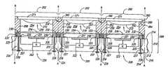
- FIG. 2is a side cross sectional view illustrating an assembly 200 having a plurality of microelectronic imagers 202 that have been packaged at the wafer-level in accordance with several embodiments of the invention.
- the embodiment of the assembly 200 shown in FIG. 2includes an imager workpiece 210 , optics supports 250 on the imager workpiece 210 , and optical devices 270 attached to the optics supports 250 .
- the assembly 200is typically manufactured by providing the imager workpiece 210 , constructing the optics supports 250 on the imager workpiece 210 , and then attaching the optical devices 270 to the optics supports 250 .
- the optics supports 250 and the optical devices 270can be assembled using automated handling equipment before cutting the imager workpiece 210 in accordance with several embodiments of the invention.
- the imager workpiece 210includes a first substrate 212 having a front side 214 and a back side 216 .
- the imager workpiece 210further includes a plurality of imaging dies 220 formed on and/or in the first substrate 212 .
- Individual imaging dies 220can include an image sensor 221 , integrated circuitry (IC) 222 operatively coupled to the image sensor 221 , and external contacts 224 electrically coupled to the integrated circuitry 222 .
- the image sensors 221can be CMOS devices or CCD image sensors for capturing pictures or other images in the visible spectrum, but the image sensors 221 can detect radiation in other spectrums (e.g., IR or UV ranges).
- Each external contact 224can include a terminal 225 (e.g., bond-pad), a contact pad 226 (e.g., ball-pad), and a through-wafer interconnect 227 coupling the terminal 225 to the contact pad 226 .
- the terminal 225is shown at the front side 214 , it can also be at an intermediate depth within the first substrate 212 .
- the through-wafer interconnects 227can be formed according to the processes disclosed in U.S.
- the imaging dies 220can further include spacers 230 projecting from the front side 214 of the first substrate 212 .
- the spacers 230can be conductive elements that project upwardly from the interconnects 227 .
- the spacers 230can alternatively be dielectric elements deposited onto the first substrate 212 or manufactured separately from the first substrate and adhered to the front side 214 .
- the imaging workpiece 210further includes a sealant 232 around an outer perimeter portion of the spacers 230 and a cover 234 attached to the spacers.
- the cover 234can be glass, quartz, or another suitable material that is transmissive to the desired spectrum of radiation.
- the cover 234for example, can further include one or more anti-reflective films and/or filters. Additionally, the cover 234 can be a single pane covering a plurality of the dies 220 as shown in FIG. 2 , or the cover 234 can have individual panes over each die 220 .
- the assembly 200further includes a plurality of the optics supports 250 on the imager workpiece 210 and a plurality of the optical devices 270 .
- the optics supports 250include bearing elements 260 that interface with the optical devices 270 .
- the bearing elements 260can include an alignment surface 262 and a reference surface 264 .
- the optical devices 270can include a second substrate 271 and an optics element 272 carried by the second substrate 271 .
- the second substrate 271is typically a window that is transmissive to the selected radiation, and the optics elements 272 can include focus lenses, dispersion lenses, pin-hole lenses, filters and/or anti-reflective films.
- the bearing elements 260interface with the second substrates 271 to (a) align the optics elements 272 with corresponding image sensors 221 , and (b) space the optics elements 272 apart from corresponding image sensors 221 by a desired distance. More specifically, the alignment surface 262 aligns the optics elements 272 and the reference surface 264 spaces the optics elements 272 apart from the image sensors 221 by the desired focal distance.
- the embodiment of the assembly 200 shown in FIG. 2is fabricated at the wafer level such that several imagers 202 are packaged before singulating (e.g., cutting) the first substrate 212 to separate the individual image sensors 202 from each other.
- One aspect of wafer-level packagingis using automated handling equipment to install the optical devices 270 such that the optics elements 272 are aligned with and spaced apart from the corresponding image sensors. This is achieved, in part, by constructing the support members 250 using fast, accurate processes.
- FIGS. 3A-7Cillustrate several embodiments of methods for (a) constructing the optics supports 250 and (b) mounting the optical devices 270 to the optics supports 250 for wafer-level packaging of microelectronic imagers.
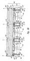
- FIGS. 3A-3Eillustrate stages in one embodiment of a method for forming optics supports that accurately position optical devices with respect to corresponding image sensors.
- this embodiment of the methodincludes depositing a support material layer 310 onto the cover 234 .
- the support material layer 310can be deposited onto the cover 234 using vapor deposition processes (e.g., chemical vapor deposition or physical vapor deposition), three-dimensional stereolithography processes, spin-on techniques, spraying techniques, molding or other processes.
- the support material layer 310can alternatively be formed separately from the workpiece 210 and then attached to the cover 234 .
- the support material layer 310has an upper surface 312 at a desired distance from the cover 234 to define a reference plane relative to the image sensors 221 .
- the upper surface 312can be formed at a precise distance from the cover 234 by planarizing the support material layer 310 using chemical-mechanical planarization. In several embodiments, however, the upper surface 312 can be formed at the desired distance from the cover 234 in the deposition process without planarizing the support material layer 310 .
- the support material layer 310can be composed of polymeric materials, ceramics, metals and/or other suitable materials.
- the bearing elements 260are then etched into the upper portion of the support material layer 310 .
- a resist layer 320is deposited onto the support material layer 310 and patterned to have openings 322 .
- an upper portion of the support material layer 310is then etched to a desired depth to form the alignment surfaces 262 at a desired location relative to the corresponding image sensors 221 .
- the support material layer 310can be etched to an intermediate depth using a first etch, such as an anisotropic etch.
- the alignment surfaces 262are laterally spaced apart from alignment axes C-C of corresponding image sensors 221 by a precise distance to engage the edges of the second substrates 271 ( FIG. 2 ) and align the optics elements 272 ( FIG. 2 ) with corresponding imager sensors 221 .
- the reference surfaces 264 of the bearing elements 260 and the openings 254 of the optics supportsare then formed from the remaining portion of the support material layer 310 .
- a second resist layer 330is deposited onto the support material layer 310 and patterned to have openings 332 .
- the exposed portions of the support material layer 310are then etched through the openings 332 .
- this second etchforms the sidewalls 252 so that they are superimposed relative to a perimeter zone around corresponding image sensors 221 .
- the sidewalls 252shape the openings 254 so that they are aligned with corresponding image sensors 221 .
- the second etch shown in FIG. 3Ealso forms the reference surfaces 264 of the bearing elements 260 at a desired reference distance relative to the image sensors 221 .
- the second etchcan be an anisotropic etch that is stopped at or slightly before the cover 234 .
- the optical devices 270are mounted to the optics supports 250 as shown in FIG. 2 .
- the optical devices 270 of the embodiment shown in FIG. 2have been singulated to separate the individual optical devices 270 from each other before being mounted to the optics supports 250 .
- Automatic handling equipmentcan place the individual optical devices 270 on corresponding optics supports 250 .
- individual bearing elements 260can receive the perimeter portion of one of the second substrates 271 such that the optics element 272 of each optical device 270 is at a desired position with respect to a corresponding image sensor 221 .
- the optics supports 250 fabricated as shown in FIGS. 3A-3Ehave precise dimensions to accurately position the optical devices 270 with respect to corresponding image sensors 221 .
- the upper surface 312 of the support material layer 310can be formed at a precise distance from the imager sensors 221 across the entire imager workpiece 210 because chemical-mechanical planarization and certain deposition processes are capable of forming highly planar surfaces at exact endpoints across a wafer.
- the first and second etches shown in FIGS. 3B-3Ecan accurately form the alignment surfaces 262 and the reference surfaces 264 with respect to corresponding image sensors 221 with a high degree of precision. Therefore, the bearing elements 260 have precise dimensions that are located relative to the image sensors to position the optical devices 270 ( FIG. 2 ) within very tight tolerances. This allows automated handling equipment to attach the optical devices to the imagining units at the wafer level without manually adjusting the focal distance.
- the embodiment of the method illustrated in FIGS. 3A-3Eis also efficient in that it has a relatively high throughput and uses existing equipment and processes in a semiconductor fabrication facility.
- the deposition, chemical-mechanical planarization and etching proceduresare established processes that are used to manufacture semiconductor devices having feature sizes of 0.11 ⁇ m or less.
- the optics supports 250can be formed in a process flow for manufacturing semiconductor devices.
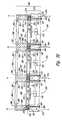
- FIGS. 4A and 4Billustrate a method for fabricating the optics supports 250 in accordance with another embodiment of the invention.
- the optics supports 250can be formed separately from the imager workpiece 210 and then attached to the imager workpiece 210 at the wafer level.
- the optics supports 250can be made from a support material layer 410 composed of a polymeric material, glass, or other suitable material.
- the bearing elements 260 and the openings 254can be formed by injection molding the support material.
- a polymeric material or glasscan be molded to form the optics supports 250 having the openings 254 and the bearing elements 260 .
- the support material layer 410can initially be a solid plate or wafer in which the openings 254 and the bearing elements 260 are formed by etching, machining and/or ablating the support material layer 410 .
- the support elements 250 in this embodimentinclude footings 412 on the backside of the support material layer 410 .
- FIG. 4Billustrates another stage in this embodiment in which the footings 412 of the support members 250 are attached to the cover 234 .
- the footings 412can be secured to the cover 234 using an adhesive 420 .
- the optics supports 250are accordingly constructed on the imager workpiece 210 by attaching a plurality of the optics supports 250 to the cover 234 before singulating the imager workpiece 210 .
- the optical devices 270( FIG. 2 ) can then be attached to the optics supports 250 as explained above.
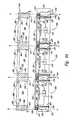
- FIG. 5illustrates a method for forming a plurality of optics supports 550 in accordance with another embodiment of the invention.
- the optics supports 550are formed by depositing a seed layer 510 of conductive material onto the cover 234 and patterning the seed layer 510 to form electrically conductive regions on top of the cover 234 .
- the electrically conductive regions of the seed layer 510are typically superimposed over a peripheral zone around the image sensors 221 .
- An electrical potentialis then applied to the seed layer 510 while the workpiece 210 is placed in a bath of plating material.
- a plurality of optical devices 570can then be attached to the optics supports 550 .
- the optical devices 570have optics elements 572 attached to a common second substrate 571 .
- the bearing elements 560 in this embodimentspace the optics elements 572 apart from corresponding image sensors 221 by a desired focal distance.
- the optics elements 572are aligned with corresponding image sensors 221 using the automated handling equipment to position the second substrate 571 in a desired alignment with the imager workpiece 210 .
- FIG. 6illustrates another method for constructing optics supports on the imager workpiece 210 in accordance with another embodiment of the invention.
- the optics supports 650are constructed on the imager workpiece 210 in accordance with any of the methods described above with respect to FIGS. 3A-5 .
- the optics support 650can be formed by depositing a support material layer onto the cover 234 and then etching the support material layer to form the openings 254 , the bearing elements 260 , and gaps 652 between individual optics supports 650 .
- the optics supports 650can be formed separately from the imager workpiece 210 as described above with reference to FIGS. 4 A-B or electroplated onto the workpiece 210 as described above with reference to FIG. 5 .
- the optics supports 650accordingly differ from those shown in FIGS. 3A-5 in that the optics supports 650 are separated from each other by the gaps 652 .
- FIGS. 7A-7Cillustrate another embodiment of forming optics elements for installing optical devices onto the imager workpiece 210 in accordance with the invention.
- the imager workpiece 210 in this embodimentdoes not include the spacers 230 and the cover 234 .
- a protective layer 702is deposited over the front side 214 of the first substrate 212 .
- the protective layer 702can be parylene, an oxide, or another suitable dielectric material.
- the protective layer 702can be transparent, semi-transparent or opaque to the selected radiation for operating the image sensors 221 depending upon the particular application.
- a support material layer 710is then formed on top of the protective layer 702 in the same manner that the support material layer 310 is formed on top of the cover 234 as described above with reference to FIG. 3A .
- the support material layer 710is then etched to form optics supports 750 with bearing elements 260 and openings 254 as shown in FIG. 7B .
- the second etch for forming the hole 254can be selective to the support material layer 710 ( FIG. 7A ) such that it does not etch the protective material 702 .
- the optical devicescan be mounted to the optics support 750 at this point.
- FIG. 7Cillustrates a subsequent processing step that is used in embodiments in which the protective layer 702 is not sufficiently transmissive to the desired radiation.
- the protective layer 702is etched to expose the image sensors 221 to the opening 254 .
- the optical devicescan then be attached to the optics support 750 .
- the optics supports 750are constructed on the imager workpiece 210 so that they project directly from the first substrate 212 .
- the optics supports 250 / 550 / 650 / 750are constructed above the first substrate 212 in the sense that they are either directly on the first substrate 212 or on a cover 234 over the first substrate 212 .
Landscapes
- Solid State Image Pick-Up Elements (AREA)
Abstract
Description
- The present invention is related to microelectronic imagers and methods for packaging microelectronic imagers. Several aspects of the present invention, more specifically, are directed toward installing optical devices in microelectronic imagers.
- Microelectronic imagers are used in digital cameras, wireless devices with picture capabilities, and many other applications. Cell phones and Personal Digital Assistants (PDAs), for example, are incorporating microelectronic imagers for capturing and sending pictures. The growth rate of microelectronic imagers has been steadily increasing as they become smaller and produce better images with higher pixel counts.
- Microelectronic imagers include image sensors that use Charged Coupled Device (CCD) systems, Complementary Metal-Oxide Semiconductor (CMOS) systems, or other systems. CCD image sensors have been widely used in digital cameras and other applications. CMOS image sensors are also quickly becoming very popular because they are expected to have low production costs, high yields and small sizes. CMOS image sensors can provide these advantages because they are manufactured using technology and equipment developed for fabricating semiconductor devices. CMOS image sensors, as well as CCD image sensors, are accordingly “packaged” to protect the delicate components and to provide external electrical contacts.
FIG. 1 is a schematic view of a conventional microelectronic imager1 with a conventional package. The imager1 includes adie 10, aninterposer 20 attached to thedie 10, and ahousing 30 attached to theinterposer 20. Thehousing 30 surrounds the periphery of the die10 and has anopening 32. The imager1 also includes atransparent cover 40 over the die10.- The die10 includes an
image sensor 12 and a plurality of bond-pads 14 electrically coupled to theimage sensor 12. Theinterposer 20 is typically a dielectric fixture having a plurality of bond-pads 22, a plurality of ball-pads 24, and traces26 electrically coupling bond-pads 22 to corresponding ball-pads 24. The ball-pads 24 are arranged in an array for surface mounting the imager1 to a board or module of another device. The bond-pads 14 on thedie 10 are electrically coupled to the bond-pads 22 on theinterposer 20 by wire-bonds 28 to provide electrical pathways between the bond-pads 14 and the ball-pads 24. Theinterposer 20 can alternatively be a lead frame or ceramic fixture. - The imager1 shown in
FIG. 1 also has an optics unit including asupport 50 attached to thehousing 30 and abarrel 60 adjustably attached to thesupport 50. Thesupport 50 can includeinternal threads 52, and thebarrel 60 can includeexternal threads 62 engaged with theinternal threads 52. The optics unit also includes alens 70 carried by thebarrel 60. - One problem with packaging conventional microelectronic imagers is that it is difficult to accurately align the lens with the image sensor. Referring to
FIG. 1 , the centerline of thelens 70 should be aligned with the centerline of theimage sensor 12 within very tight tolerances. For example, as microelectronic imagers have higher pixel counts and smaller sizes, the centerline of thelens 70 is often required to be within 50 μm of the centerline of theimage sensor 12. This is difficult to achieve with conventional imagers because thesupport 50 may not be positioned accurately on thehousing 30, and thebarrel 60 is manually threaded onto thesupport 50. Therefore, there is a need to align lenses with image sensors with greater precision in more sophisticated generations of microelectronic imagers. - Another problem of packaging conventional microelectronic imagers is that positioning the lens at a desired focus distance from the image sensor is time-consuming and may be inaccurate. The
lens 70 shown inFIG. 1 is spaced apart from theimage sensor 12 at a desired distance by rotating the barrel60 (arrow R) to adjust the elevation (arrow E) of thelens 70 relative to theimage sensor 12. In practice, an operator manually rotates thebarrel 60 by hand while watching an output of the imager1 on a display until the picture is focused based on the operator's subjective evaluation. The operator then adheres thebarrel 60 to thesupport 50 to secure thelens 70 in a position where it is spaced apart from theimage sensor 12 by a suitable focus distance. This process is problematic because it is exceptionally time-consuming, subject to operator errors, and subject to axial misalignment between thesupport 50 and thebarrel 60. - Yet another concern of conventional microelectronic imagers is that they have relatively large footprints and occupy a significant amount of vertical space (i.e., high profiles). The footprint of the imager in
FIG. 1 is the surface area of the bottom of theinterposer 20. This is typically much larger than the surface area of thedie 10 and can be a limiting factor in the design and marketability of picture cell phones or PDAs because these devices are continually shrinking to be more portable. Therefore, there is a need to provide microelectronic imagers with smaller footprints and lower profiles. - Yet another concern of conventional microelectronic imagers is the manufacturing costs for packaging the dies. The imager1 shown in
FIG. 1 is relatively expensive because manually adjusting thelens 70 relative to theimage sensor 12 is very inefficient and subject to error. The conventional imager1 shown inFIG. 1 is also expensive because eachcover 40 is individually attached to thehousing 30, and eachhousing 30 is individually attached to aninterposer 20. Moreover, thesupport 50 andbarrel 60 are assembled separately for eachdie 10 individually after the dies have been singulated from a wafer and attached to theinterposer 20. Therefore, there is a significant need to enhance the efficiency, reliability and precision of packaging microelectronic imagers. FIG. 1 is a schematic side cross-sectional view of a packaged microelectronic imager in accordance with the prior art.FIG. 2 is a cross-sectional view illustrating a plurality of imagers packaged at the wafer level in accordance with an embodiment of the invention.FIGS. 3A-3E are schematic side cross-sectional views illustrating stages of a method of installing optical devices in accordance with an embodiment of the invention.FIGS. 4A and 4B are schematic side cross-sectional views illustrating stages of a method for installing optical devices in accordance with another embodiment of the invention.FIG. 5 is a schematic cross-sectional illustrating a method of installing optical devices in accordance with yet another embodiment of the invention.FIG. 6 is a schematic side cross-sectional view of a method for installing optical devices in accordance with still another embodiment of the invention.FIG. 7A-7C are schematic side cross-sectional views illustrating stages of a method for installing optical devices in accordance with yet another embodiment of the invention.- A. Overview
- The following disclosure describes several embodiments of methods for assembling optical devices with microelectronic imaging units and microelectronic imagers that are formed using such methods. One aspect of the invention is directed toward methods of manufacturing microelectronic imagers. An embodiment of one such method comprises providing an imager workpiece and constructing optics supports on the imager workpiece. The imager workpiece has a plurality of imaging dies that include image sensors and external contacts operatively coupled to the image sensors. The imaging dies can be on and/or in a first substrate such that the image sensors are at a front side of the first substrate. The optics supports are constructed on the imager workpiece before cutting the imager workpiece. The optics supports, for example, can be constructed on the first substrate or on a cover attached to the first substrate. The optics supports include openings aligned with corresponding image sensors and bearing elements at reference locations relative to corresponding image sensors. The method can further include attaching optical devices to the bearing elements. The optical devices, for example, can include focus lenses, dispersion lenses, pin-hole lenses, filters and/or anti-reflective coatings. In several embodiments, the optical devices are generally attached to the bearing elements before cutting the first substrate.
- Another aspect of the invention is directed toward a microelectronic imager assembly. One embodiment of such a microelectronic imager assembly comprises a workpiece including a substrate and a plurality of imaging dies on and/or in the substrate. The substrate includes a front side and a back side, and the imaging dies comprise imaging sensors at the front side of the substrate and external contacts operatively coupled to the image sensors. The microelectronic imager assembly further comprises optics supports superimposed relative to the imaging dies. The optics supports can be directly on the substrate or on a cover over the substrate. Individual optics supports can have (a) an opening aligned with one of the image sensors, and (b) a bearing element at a reference distance from the image sensor. The microelectronic imager assembly can further include optical devices mounted or otherwise carried by the optics supports. The optical devices can include optics elements that are aligned with corresponding image sensors on the imaging dies.
- Several details of specific embodiments of the invention are described below with reference to CMOS imagers to provide a thorough understanding of these embodiments. CCD imagers or other types of sensors, however, can be used instead of the CMOS imagers in other embodiments of the invention. Several details describing well-known structures often associated with microelectronic devices may not be set forth in the following description for the purposes of brevity. Moreover, other embodiments of the invention can have different configurations or different components than those described in this section. As such, other embodiments of the invention may have additional elements or may not include all of the elements shown and described below with reference to
FIGS. 2-7C . - B. Microelectronic Imagers Packaged at the Wafer-Level
FIG. 2 is a side cross sectional view illustrating anassembly 200 having a plurality ofmicroelectronic imagers 202 that have been packaged at the wafer-level in accordance with several embodiments of the invention. The embodiment of theassembly 200 shown inFIG. 2 includes animager workpiece 210, optics supports250 on theimager workpiece 210, andoptical devices 270 attached to the optics supports250. Theassembly 200 is typically manufactured by providing theimager workpiece 210, constructing the optics supports250 on theimager workpiece 210, and then attaching theoptical devices 270 to the optics supports250. The optics supports250 and theoptical devices 270 can be assembled using automated handling equipment before cutting theimager workpiece 210 in accordance with several embodiments of the invention.- The
imager workpiece 210 includes afirst substrate 212 having afront side 214 and aback side 216. Theimager workpiece 210 further includes a plurality of imaging dies220 formed on and/or in thefirst substrate 212. Individual imaging dies220 can include animage sensor 221, integrated circuitry (IC)222 operatively coupled to theimage sensor 221, andexternal contacts 224 electrically coupled to theintegrated circuitry 222. Theimage sensors 221 can be CMOS devices or CCD image sensors for capturing pictures or other images in the visible spectrum, but theimage sensors 221 can detect radiation in other spectrums (e.g., IR or UV ranges). The embodiment of theexternal contacts 224 shown inFIG. 2 provides a small array of ball-pads within the footprint of the individual imaging dies220. Eachexternal contact 224, for example, can include a terminal225 (e.g., bond-pad), a contact pad226 (e.g., ball-pad), and a through-wafer interconnect 227 coupling the terminal225 to thecontact pad 226. Although the terminal225 is shown at thefront side 214, it can also be at an intermediate depth within thefirst substrate 212. The through-wafer interconnects 227 can be formed according to the processes disclosed in U.S. patent application Ser. No. 10/713,878, entitled Microelectronic Devices, Methods for Forming Vias in Microelectronic Devices, and Methods for Packaging Microelectronic Devices, filed on Nov. 13, 2003 (Perkins Cole Docket No. 10829.8742US00), which is incorporated by reference herein in its entirety. Other embodiments of external contacts can include contacts having traces that wrap around the side of thefirst substrate 212. - The imaging dies220 can further include
spacers 230 projecting from thefront side 214 of thefirst substrate 212. Thespacers 230 can be conductive elements that project upwardly from theinterconnects 227. Thespacers 230 can alternatively be dielectric elements deposited onto thefirst substrate 212 or manufactured separately from the first substrate and adhered to thefront side 214. - The
imaging workpiece 210 further includes asealant 232 around an outer perimeter portion of thespacers 230 and acover 234 attached to the spacers. Thecover 234 can be glass, quartz, or another suitable material that is transmissive to the desired spectrum of radiation. Thecover 234, for example, can further include one or more anti-reflective films and/or filters. Additionally, thecover 234 can be a single pane covering a plurality of the dies220 as shown inFIG. 2 , or thecover 234 can have individual panes over each die220. - The
assembly 200 further includes a plurality of the optics supports250 on theimager workpiece 210 and a plurality of theoptical devices 270. The optics supports250 include bearingelements 260 that interface with theoptical devices 270. The bearingelements 260, for example, can include analignment surface 262 and areference surface 264. Theoptical devices 270 can include asecond substrate 271 and anoptics element 272 carried by thesecond substrate 271. Thesecond substrate 271 is typically a window that is transmissive to the selected radiation, and theoptics elements 272 can include focus lenses, dispersion lenses, pin-hole lenses, filters and/or anti-reflective films. The bearingelements 260 interface with thesecond substrates 271 to (a) align theoptics elements 272 withcorresponding image sensors 221, and (b) space theoptics elements 272 apart from correspondingimage sensors 221 by a desired distance. More specifically, thealignment surface 262 aligns theoptics elements 272 and thereference surface 264 spaces theoptics elements 272 apart from theimage sensors 221 by the desired focal distance. - The embodiment of the
assembly 200 shown inFIG. 2 is fabricated at the wafer level such thatseveral imagers 202 are packaged before singulating (e.g., cutting) thefirst substrate 212 to separate theindividual image sensors 202 from each other. One aspect of wafer-level packaging is using automated handling equipment to install theoptical devices 270 such that theoptics elements 272 are aligned with and spaced apart from the corresponding image sensors. This is achieved, in part, by constructing thesupport members 250 using fast, accurate processes.FIGS. 3A-7C illustrate several embodiments of methods for (a) constructing the optics supports250 and (b) mounting theoptical devices 270 to the optics supports250 for wafer-level packaging of microelectronic imagers. - C. Optics Supports and Optical Devices
FIGS. 3A-3E illustrate stages in one embodiment of a method for forming optics supports that accurately position optical devices with respect to corresponding image sensors. Referring toFIG. 3A , this embodiment of the method includes depositing asupport material layer 310 onto thecover 234. Thesupport material layer 310 can be deposited onto thecover 234 using vapor deposition processes (e.g., chemical vapor deposition or physical vapor deposition), three-dimensional stereolithography processes, spin-on techniques, spraying techniques, molding or other processes. Thesupport material layer 310 can alternatively be formed separately from theworkpiece 210 and then attached to thecover 234. Thesupport material layer 310 has anupper surface 312 at a desired distance from thecover 234 to define a reference plane relative to theimage sensors 221. Theupper surface 312 can be formed at a precise distance from thecover 234 by planarizing thesupport material layer 310 using chemical-mechanical planarization. In several embodiments, however, theupper surface 312 can be formed at the desired distance from thecover 234 in the deposition process without planarizing thesupport material layer 310. Thesupport material layer 310 can be composed of polymeric materials, ceramics, metals and/or other suitable materials.- The bearing elements260 (
FIG. 2 ) are then etched into the upper portion of thesupport material layer 310. Referring toFIG. 3B , for example, a resistlayer 320 is deposited onto thesupport material layer 310 and patterned to haveopenings 322. As shown inFIG. 3C , an upper portion of thesupport material layer 310 is then etched to a desired depth to form the alignment surfaces262 at a desired location relative to thecorresponding image sensors 221. Thesupport material layer 310 can be etched to an intermediate depth using a first etch, such as an anisotropic etch. The alignment surfaces262 are laterally spaced apart from alignment axes C-C ofcorresponding image sensors 221 by a precise distance to engage the edges of the second substrates271 (FIG. 2 ) and align the optics elements272 (FIG. 2 ) withcorresponding imager sensors 221. - The reference surfaces264 of the bearing
elements 260 and theopenings 254 of the optics supports are then formed from the remaining portion of thesupport material layer 310. Referring toFIG. 3D , a second resistlayer 330 is deposited onto thesupport material layer 310 and patterned to haveopenings 332. The exposed portions of thesupport material layer 310 are then etched through theopenings 332. Referring toFIG. 3E , this second etch forms thesidewalls 252 so that they are superimposed relative to a perimeter zone around correspondingimage sensors 221. Thesidewalls 252 shape theopenings 254 so that they are aligned withcorresponding image sensors 221. The second etch shown inFIG. 3E also forms the reference surfaces264 of the bearingelements 260 at a desired reference distance relative to theimage sensors 221. The second etch can be an anisotropic etch that is stopped at or slightly before thecover 234. - After the optics supports250 have been formed as shown in
FIG. 3E , theoptical devices 270 are mounted to the optics supports250 as shown inFIG. 2 . Theoptical devices 270 of the embodiment shown inFIG. 2 have been singulated to separate the individualoptical devices 270 from each other before being mounted to the optics supports250. Automatic handling equipment can place the individualoptical devices 270 on corresponding optics supports250. More specifically,individual bearing elements 260 can receive the perimeter portion of one of thesecond substrates 271 such that theoptics element 272 of eachoptical device 270 is at a desired position with respect to acorresponding image sensor 221. - The optics supports250 fabricated as shown in
FIGS. 3A-3E have precise dimensions to accurately position theoptical devices 270 with respect tocorresponding image sensors 221. For example, theupper surface 312 of thesupport material layer 310 can be formed at a precise distance from theimager sensors 221 across theentire imager workpiece 210 because chemical-mechanical planarization and certain deposition processes are capable of forming highly planar surfaces at exact endpoints across a wafer. Additionally, the first and second etches shown inFIGS. 3B-3E can accurately form the alignment surfaces262 and the reference surfaces264 with respect tocorresponding image sensors 221 with a high degree of precision. Therefore, the bearingelements 260 have precise dimensions that are located relative to the image sensors to position the optical devices270 (FIG. 2 ) within very tight tolerances. This allows automated handling equipment to attach the optical devices to the imagining units at the wafer level without manually adjusting the focal distance. - The embodiment of the method illustrated in
FIGS. 3A-3E is also efficient in that it has a relatively high throughput and uses existing equipment and processes in a semiconductor fabrication facility. The deposition, chemical-mechanical planarization and etching procedures are established processes that are used to manufacture semiconductor devices having feature sizes of 0.11 μm or less. As a result, the optics supports250 can be formed in a process flow for manufacturing semiconductor devices. FIGS. 4A and 4B illustrate a method for fabricating the optics supports250 in accordance with another embodiment of the invention. Referring toFIG. 4A , the optics supports250 can be formed separately from theimager workpiece 210 and then attached to theimager workpiece 210 at the wafer level. The optics supports250, for example, can be made from asupport material layer 410 composed of a polymeric material, glass, or other suitable material. The bearingelements 260 and theopenings 254 can be formed by injection molding the support material. For example, a polymeric material or glass can be molded to form the optics supports250 having theopenings 254 and the bearingelements 260. In another embodiment, thesupport material layer 410 can initially be a solid plate or wafer in which theopenings 254 and the bearingelements 260 are formed by etching, machining and/or ablating thesupport material layer 410. Thesupport elements 250 in this embodiment includefootings 412 on the backside of thesupport material layer 410.FIG. 4B illustrates another stage in this embodiment in which thefootings 412 of thesupport members 250 are attached to thecover 234. Thefootings 412 can be secured to thecover 234 using an adhesive420. The optics supports250 are accordingly constructed on theimager workpiece 210 by attaching a plurality of the optics supports250 to thecover 234 before singulating theimager workpiece 210. The optical devices270 (FIG. 2 ) can then be attached to the optics supports250 as explained above.FIG. 5 illustrates a method for forming a plurality of optics supports550 in accordance with another embodiment of the invention. In this embodiment, the optics supports550 are formed by depositing aseed layer 510 of conductive material onto thecover 234 and patterning theseed layer 510 to form electrically conductive regions on top of thecover 234. The electrically conductive regions of theseed layer 510 are typically superimposed over a peripheral zone around theimage sensors 221. An electrical potential is then applied to theseed layer 510 while theworkpiece 210 is placed in a bath of plating material. The material plates on top of theseed layer 510 to form the optics supports550 havingbearing elements 560 at a desired elevation with respect to theimage sensors 221. A plurality ofoptical devices 570 can then be attached to the optics supports550. In this embodiment, theoptical devices 570 haveoptics elements 572 attached to a commonsecond substrate 571. The bearingelements 560 in this embodiment space theoptics elements 572 apart from correspondingimage sensors 221 by a desired focal distance. Theoptics elements 572 are aligned withcorresponding image sensors 221 using the automated handling equipment to position thesecond substrate 571 in a desired alignment with theimager workpiece 210.FIG. 6 illustrates another method for constructing optics supports on theimager workpiece 210 in accordance with another embodiment of the invention. In this embodiment, the optics supports650 are constructed on theimager workpiece 210 in accordance with any of the methods described above with respect toFIGS. 3A-5 . For example, theoptics support 650 can be formed by depositing a support material layer onto thecover 234 and then etching the support material layer to form theopenings 254, the bearingelements 260, andgaps 652 between individual optics supports650. Alternatively, the optics supports650 can be formed separately from theimager workpiece 210 as described above with reference to FIGS.4A-B or electroplated onto theworkpiece 210 as described above with reference toFIG. 5 . The optics supports650 accordingly differ from those shown inFIGS. 3A-5 in that the optics supports650 are separated from each other by thegaps 652.FIGS. 7A-7C illustrate another embodiment of forming optics elements for installing optical devices onto theimager workpiece 210 in accordance with the invention. Referring toFIG. 7A , theimager workpiece 210 in this embodiment does not include thespacers 230 and thecover 234. Instead, aprotective layer 702 is deposited over thefront side 214 of thefirst substrate 212. Theprotective layer 702 can be parylene, an oxide, or another suitable dielectric material. Theprotective layer 702 can be transparent, semi-transparent or opaque to the selected radiation for operating theimage sensors 221 depending upon the particular application. Asupport material layer 710 is then formed on top of theprotective layer 702 in the same manner that thesupport material layer 310 is formed on top of thecover 234 as described above with reference toFIG. 3A . Thesupport material layer 710 is then etched to form optics supports750 with bearingelements 260 andopenings 254 as shown inFIG. 7B . The second etch for forming thehole 254 can be selective to the support material layer710 (FIG. 7A ) such that it does not etch theprotective material 702. In embodiments in which theprotective layer 702 is composed of a material that is suitably transmissive to the desired radiation, the optical devices can be mounted to theoptics support 750 at this point.FIG. 7C illustrates a subsequent processing step that is used in embodiments in which theprotective layer 702 is not sufficiently transmissive to the desired radiation. In this embodiment, theprotective layer 702 is etched to expose theimage sensors 221 to theopening 254. The optical devices can then be attached to theoptics support 750. In either of the embodiments shown inFIG. 7B or7C, the optics supports750 are constructed on theimager workpiece 210 so that they project directly from thefirst substrate 212. As such, in any of the embodiments shown above with respect toFIGS. 3A-7C , the optics supports250/550/650/750 are constructed above thefirst substrate 212 in the sense that they are either directly on thefirst substrate 212 or on acover 234 over thefirst substrate 212.- From the foregoing, it will be appreciated that specific embodiments of the invention have been described herein for purposes of illustration, but that various modifications may be made without deviating from the spirit and scope of the invention. Accordingly, the invention is not limited except as by the appended claims.
Claims (30)
Priority Applications (3)
| Application Number | Priority Date | Filing Date | Title |
|---|---|---|---|
| US11/476,015US7265330B2 (en) | 2004-07-19 | 2006-06-28 | Microelectronic imagers with optical devices and methods of manufacturing such microelectronic imagers |
| US11/727,545US7504615B2 (en) | 2004-07-19 | 2007-03-27 | Microelectronic imagers with optical devices and methods of manufacturing such microelectronic imagers |
| US12/390,195US7709776B2 (en) | 2004-07-19 | 2009-02-20 | Microelectronic imagers with optical devices and methods of manufacturing such microelectronic imagers |
Applications Claiming Priority (2)
| Application Number | Priority Date | Filing Date | Title |
|---|---|---|---|
| US10/894,262US7189954B2 (en) | 2004-07-19 | 2004-07-19 | Microelectronic imagers with optical devices and methods of manufacturing such microelectronic imagers |
| US11/476,015US7265330B2 (en) | 2004-07-19 | 2006-06-28 | Microelectronic imagers with optical devices and methods of manufacturing such microelectronic imagers |
Related Parent Applications (1)
| Application Number | Title | Priority Date | Filing Date |
|---|---|---|---|
| US10/894,262DivisionUS7189954B2 (en) | 2004-07-19 | 2004-07-19 | Microelectronic imagers with optical devices and methods of manufacturing such microelectronic imagers |
Related Child Applications (1)
| Application Number | Title | Priority Date | Filing Date |
|---|---|---|---|
| US11/727,545ContinuationUS7504615B2 (en) | 2004-07-19 | 2007-03-27 | Microelectronic imagers with optical devices and methods of manufacturing such microelectronic imagers |
Publications (2)
| Publication Number | Publication Date |
|---|---|
| US20060243889A1true US20060243889A1 (en) | 2006-11-02 |
| US7265330B2 US7265330B2 (en) | 2007-09-04 |
Family
ID=35598481
Family Applications (4)
| Application Number | Title | Priority Date | Filing Date |
|---|---|---|---|
| US10/894,262Expired - LifetimeUS7189954B2 (en) | 2004-07-19 | 2004-07-19 | Microelectronic imagers with optical devices and methods of manufacturing such microelectronic imagers |
| US11/476,015Expired - LifetimeUS7265330B2 (en) | 2004-07-19 | 2006-06-28 | Microelectronic imagers with optical devices and methods of manufacturing such microelectronic imagers |
| US11/727,545Expired - LifetimeUS7504615B2 (en) | 2004-07-19 | 2007-03-27 | Microelectronic imagers with optical devices and methods of manufacturing such microelectronic imagers |
| US12/390,195Expired - LifetimeUS7709776B2 (en) | 2004-07-19 | 2009-02-20 | Microelectronic imagers with optical devices and methods of manufacturing such microelectronic imagers |
Family Applications Before (1)
| Application Number | Title | Priority Date | Filing Date |
|---|---|---|---|
| US10/894,262Expired - LifetimeUS7189954B2 (en) | 2004-07-19 | 2004-07-19 | Microelectronic imagers with optical devices and methods of manufacturing such microelectronic imagers |
Family Applications After (2)
| Application Number | Title | Priority Date | Filing Date |
|---|---|---|---|
| US11/727,545Expired - LifetimeUS7504615B2 (en) | 2004-07-19 | 2007-03-27 | Microelectronic imagers with optical devices and methods of manufacturing such microelectronic imagers |
| US12/390,195Expired - LifetimeUS7709776B2 (en) | 2004-07-19 | 2009-02-20 | Microelectronic imagers with optical devices and methods of manufacturing such microelectronic imagers |
Country Status (1)
| Country | Link |
|---|---|
| US (4) | US7189954B2 (en) |
Cited By (68)
| Publication number | Priority date | Publication date | Assignee | Title |
|---|---|---|---|---|
| US20090032925A1 (en)* | 2007-07-31 | 2009-02-05 | England Luke G | Packaging with a connection structure |
| US20110080487A1 (en)* | 2008-05-20 | 2011-04-07 | Pelican Imaging Corporation | Capturing and processing of images using monolithic camera array with heterogeneous imagers |
| US8619082B1 (en) | 2012-08-21 | 2013-12-31 | Pelican Imaging Corporation | Systems and methods for parallax detection and correction in images captured using array cameras that contain occlusions using subsets of images to perform depth estimation |
| US8804255B2 (en) | 2011-06-28 | 2014-08-12 | Pelican Imaging Corporation | Optical arrangements for use with an array camera |
| US8831367B2 (en) | 2011-09-28 | 2014-09-09 | Pelican Imaging Corporation | Systems and methods for decoding light field image files |
| US8861089B2 (en) | 2009-11-20 | 2014-10-14 | Pelican Imaging Corporation | Capturing and processing of images using monolithic camera array with heterogeneous imagers |
| US8866912B2 (en) | 2013-03-10 | 2014-10-21 | Pelican Imaging Corporation | System and methods for calibration of an array camera using a single captured image |
| US8878950B2 (en) | 2010-12-14 | 2014-11-04 | Pelican Imaging Corporation | Systems and methods for synthesizing high resolution images using super-resolution processes |
| US8885059B1 (en) | 2008-05-20 | 2014-11-11 | Pelican Imaging Corporation | Systems and methods for measuring depth using images captured by camera arrays |
| US8928793B2 (en) | 2010-05-12 | 2015-01-06 | Pelican Imaging Corporation | Imager array interfaces |
| US9100586B2 (en) | 2013-03-14 | 2015-08-04 | Pelican Imaging Corporation | Systems and methods for photometric normalization in array cameras |
| US9100635B2 (en) | 2012-06-28 | 2015-08-04 | Pelican Imaging Corporation | Systems and methods for detecting defective camera arrays and optic arrays |
| US9106784B2 (en) | 2013-03-13 | 2015-08-11 | Pelican Imaging Corporation | Systems and methods for controlling aliasing in images captured by an array camera for use in super-resolution processing |
| US9124831B2 (en) | 2013-03-13 | 2015-09-01 | Pelican Imaging Corporation | System and methods for calibration of an array camera |
| US9143711B2 (en) | 2012-11-13 | 2015-09-22 | Pelican Imaging Corporation | Systems and methods for array camera focal plane control |
| US9185276B2 (en) | 2013-11-07 | 2015-11-10 | Pelican Imaging Corporation | Methods of manufacturing array camera modules incorporating independently aligned lens stacks |
| US9197821B2 (en) | 2011-05-11 | 2015-11-24 | Pelican Imaging Corporation | Systems and methods for transmitting and receiving array camera image data |
| US9210392B2 (en) | 2012-05-01 | 2015-12-08 | Pelican Imaging Coporation | Camera modules patterned with pi filter groups |
| US9214013B2 (en) | 2012-09-14 | 2015-12-15 | Pelican Imaging Corporation | Systems and methods for correcting user identified artifacts in light field images |
| US9247117B2 (en) | 2014-04-07 | 2016-01-26 | Pelican Imaging Corporation | Systems and methods for correcting for warpage of a sensor array in an array camera module by introducing warpage into a focal plane of a lens stack array |
| US9253380B2 (en) | 2013-02-24 | 2016-02-02 | Pelican Imaging Corporation | Thin form factor computational array cameras and modular array cameras |
| US9412206B2 (en) | 2012-02-21 | 2016-08-09 | Pelican Imaging Corporation | Systems and methods for the manipulation of captured light field image data |
| US9426361B2 (en) | 2013-11-26 | 2016-08-23 | Pelican Imaging Corporation | Array camera configurations incorporating multiple constituent array cameras |
| US9438888B2 (en) | 2013-03-15 | 2016-09-06 | Pelican Imaging Corporation | Systems and methods for stereo imaging with camera arrays |
| US9445003B1 (en) | 2013-03-15 | 2016-09-13 | Pelican Imaging Corporation | Systems and methods for synthesizing high resolution images using image deconvolution based on motion and depth information |
| US9462164B2 (en) | 2013-02-21 | 2016-10-04 | Pelican Imaging Corporation | Systems and methods for generating compressed light field representation data using captured light fields, array geometry, and parallax information |
| US9497370B2 (en) | 2013-03-15 | 2016-11-15 | Pelican Imaging Corporation | Array camera architecture implementing quantum dot color filters |
| US9497429B2 (en) | 2013-03-15 | 2016-11-15 | Pelican Imaging Corporation | Extended color processing on pelican array cameras |
| US9516222B2 (en) | 2011-06-28 | 2016-12-06 | Kip Peli P1 Lp | Array cameras incorporating monolithic array camera modules with high MTF lens stacks for capture of images used in super-resolution processing |
| US9521319B2 (en) | 2014-06-18 | 2016-12-13 | Pelican Imaging Corporation | Array cameras and array camera modules including spectral filters disposed outside of a constituent image sensor |
| US9521416B1 (en) | 2013-03-11 | 2016-12-13 | Kip Peli P1 Lp | Systems and methods for image data compression |
| US9519972B2 (en) | 2013-03-13 | 2016-12-13 | Kip Peli P1 Lp | Systems and methods for synthesizing images from image data captured by an array camera using restricted depth of field depth maps in which depth estimation precision varies |
| US9578259B2 (en) | 2013-03-14 | 2017-02-21 | Fotonation Cayman Limited | Systems and methods for reducing motion blur in images or video in ultra low light with array cameras |
| US9633442B2 (en) | 2013-03-15 | 2017-04-25 | Fotonation Cayman Limited | Array cameras including an array camera module augmented with a separate camera |
| US9638883B1 (en) | 2013-03-04 | 2017-05-02 | Fotonation Cayman Limited | Passive alignment of array camera modules constructed from lens stack arrays and sensors based upon alignment information obtained during manufacture of array camera modules using an active alignment process |
| US9766380B2 (en) | 2012-06-30 | 2017-09-19 | Fotonation Cayman Limited | Systems and methods for manufacturing camera modules using active alignment of lens stack arrays and sensors |
| US9774789B2 (en) | 2013-03-08 | 2017-09-26 | Fotonation Cayman Limited | Systems and methods for high dynamic range imaging using array cameras |
| US9794476B2 (en) | 2011-09-19 | 2017-10-17 | Fotonation Cayman Limited | Systems and methods for controlling aliasing in images captured by an array camera for use in super resolution processing using pixel apertures |
| US9813616B2 (en) | 2012-08-23 | 2017-11-07 | Fotonation Cayman Limited | Feature based high resolution motion estimation from low resolution images captured using an array source |
| US9888194B2 (en) | 2013-03-13 | 2018-02-06 | Fotonation Cayman Limited | Array camera architecture implementing quantum film image sensors |
| US9898856B2 (en) | 2013-09-27 | 2018-02-20 | Fotonation Cayman Limited | Systems and methods for depth-assisted perspective distortion correction |
| US9942474B2 (en) | 2015-04-17 | 2018-04-10 | Fotonation Cayman Limited | Systems and methods for performing high speed video capture and depth estimation using array cameras |
| US10089740B2 (en) | 2014-03-07 | 2018-10-02 | Fotonation Limited | System and methods for depth regularization and semiautomatic interactive matting using RGB-D images |
| US10122993B2 (en) | 2013-03-15 | 2018-11-06 | Fotonation Limited | Autofocus system for a conventional camera that uses depth information from an array camera |
| US10119808B2 (en) | 2013-11-18 | 2018-11-06 | Fotonation Limited | Systems and methods for estimating depth from projected texture using camera arrays |
| US10250871B2 (en) | 2014-09-29 | 2019-04-02 | Fotonation Limited | Systems and methods for dynamic calibration of array cameras |
| US10390005B2 (en) | 2012-09-28 | 2019-08-20 | Fotonation Limited | Generating images from light fields utilizing virtual viewpoints |
| US20190259741A1 (en)* | 2015-04-20 | 2019-08-22 | Advanced Semiconductor Engineering, Inc. | Optical sensor module and method for manufacturing the same |
| US10482618B2 (en) | 2017-08-21 | 2019-11-19 | Fotonation Limited | Systems and methods for hybrid depth regularization |
| US20200099832A1 (en)* | 2018-09-21 | 2020-03-26 | Ability Opto-Electronics Technology Co.Ltd. | Optical image capturing module |
| US11270110B2 (en) | 2019-09-17 | 2022-03-08 | Boston Polarimetrics, Inc. | Systems and methods for surface modeling using polarization cues |
| US11290658B1 (en) | 2021-04-15 | 2022-03-29 | Boston Polarimetrics, Inc. | Systems and methods for camera exposure control |
| US11302012B2 (en) | 2019-11-30 | 2022-04-12 | Boston Polarimetrics, Inc. | Systems and methods for transparent object segmentation using polarization cues |
| US11386635B2 (en)* | 2020-08-25 | 2022-07-12 | Neuronbasic Technology, Inc. | Smart chip assembly capable of communicating with each other and variable array in packaging |
| US11525906B2 (en) | 2019-10-07 | 2022-12-13 | Intrinsic Innovation Llc | Systems and methods for augmentation of sensor systems and imaging systems with polarization |
| US11580667B2 (en) | 2020-01-29 | 2023-02-14 | Intrinsic Innovation Llc | Systems and methods for characterizing object pose detection and measurement systems |
| US11689813B2 (en) | 2021-07-01 | 2023-06-27 | Intrinsic Innovation Llc | Systems and methods for high dynamic range imaging using crossed polarizers |
| US11792538B2 (en) | 2008-05-20 | 2023-10-17 | Adeia Imaging Llc | Capturing and processing of images including occlusions focused on an image sensor by a lens stack array |
| US11797863B2 (en) | 2020-01-30 | 2023-10-24 | Intrinsic Innovation Llc | Systems and methods for synthesizing data for training statistical models on different imaging modalities including polarized images |
| US11953700B2 (en) | 2020-05-27 | 2024-04-09 | Intrinsic Innovation Llc | Multi-aperture polarization optical systems using beam splitters |
| US11954886B2 (en) | 2021-04-15 | 2024-04-09 | Intrinsic Innovation Llc | Systems and methods for six-degree of freedom pose estimation of deformable objects |
| US12020455B2 (en) | 2021-03-10 | 2024-06-25 | Intrinsic Innovation Llc | Systems and methods for high dynamic range image reconstruction |
| US12067746B2 (en) | 2021-05-07 | 2024-08-20 | Intrinsic Innovation Llc | Systems and methods for using computer vision to pick up small objects |
| US12069227B2 (en) | 2021-03-10 | 2024-08-20 | Intrinsic Innovation Llc | Multi-modal and multi-spectral stereo camera arrays |
| US12175741B2 (en) | 2021-06-22 | 2024-12-24 | Intrinsic Innovation Llc | Systems and methods for a vision guided end effector |
| US12172310B2 (en) | 2021-06-29 | 2024-12-24 | Intrinsic Innovation Llc | Systems and methods for picking objects using 3-D geometry and segmentation |
| US12293535B2 (en) | 2021-08-03 | 2025-05-06 | Intrinsic Innovation Llc | Systems and methods for training pose estimators in computer vision |
| US12340538B2 (en) | 2021-06-25 | 2025-06-24 | Intrinsic Innovation Llc | Systems and methods for generating and using visual datasets for training computer vision models |
Families Citing this family (38)
| Publication number | Priority date | Publication date | Assignee | Title |
|---|---|---|---|---|
| US8084866B2 (en) | 2003-12-10 | 2011-12-27 | Micron Technology, Inc. | Microelectronic devices and methods for filling vias in microelectronic devices |
| US7091124B2 (en)* | 2003-11-13 | 2006-08-15 | Micron Technology, Inc. | Methods for forming vias in microelectronic devices, and methods for packaging microelectronic devices |
| US20050247894A1 (en) | 2004-05-05 | 2005-11-10 | Watkins Charles M | Systems and methods for forming apertures in microfeature workpieces |
| US7232754B2 (en)* | 2004-06-29 | 2007-06-19 | Micron Technology, Inc. | Microelectronic devices and methods for forming interconnects in microelectronic devices |
| US7425499B2 (en)* | 2004-08-24 | 2008-09-16 | Micron Technology, Inc. | Methods for forming interconnects in vias and microelectronic workpieces including such interconnects |
| US7429494B2 (en)* | 2004-08-24 | 2008-09-30 | Micron Technology, Inc. | Microelectronic imagers with optical devices having integral reference features and methods for manufacturing such microelectronic imagers |
| SG120200A1 (en) | 2004-08-27 | 2006-03-28 | Micron Technology Inc | Slanted vias for electrical circuits on circuit boards and other substrates |
| US7300857B2 (en) | 2004-09-02 | 2007-11-27 | Micron Technology, Inc. | Through-wafer interconnects for photoimager and memory wafers |
| US7271482B2 (en)* | 2004-12-30 | 2007-09-18 | Micron Technology, Inc. | Methods for forming interconnects in microelectronic workpieces and microelectronic workpieces formed using such methods |
| US7795134B2 (en) | 2005-06-28 | 2010-09-14 | Micron Technology, Inc. | Conductive interconnect structures and formation methods using supercritical fluids |
| US7262134B2 (en) | 2005-09-01 | 2007-08-28 | Micron Technology, Inc. | Microfeature workpieces and methods for forming interconnects in microfeature workpieces |
| US7863187B2 (en) | 2005-09-01 | 2011-01-04 | Micron Technology, Inc. | Microfeature workpieces and methods for forming interconnects in microfeature workpieces |
| US7622377B2 (en) | 2005-09-01 | 2009-11-24 | Micron Technology, Inc. | Microfeature workpiece substrates having through-substrate vias, and associated methods of formation |
| US20070091746A1 (en)* | 2005-10-12 | 2007-04-26 | Storage Appliance Corporation | Optical disc for simplified data backup |
| TW200727501A (en)* | 2006-01-11 | 2007-07-16 | Advanced Semiconductor Eng | Image sensor module and method for manufacturing the same |
| US7749899B2 (en) | 2006-06-01 | 2010-07-06 | Micron Technology, Inc. | Microelectronic workpieces and methods and systems for forming interconnects in microelectronic workpieces |
| US7629249B2 (en)* | 2006-08-28 | 2009-12-08 | Micron Technology, Inc. | Microfeature workpieces having conductive interconnect structures formed by chemically reactive processes, and associated systems and methods |
| US7902643B2 (en) | 2006-08-31 | 2011-03-08 | Micron Technology, Inc. | Microfeature workpieces having interconnects and conductive backplanes, and associated systems and methods |
| WO2008060630A2 (en)* | 2006-11-17 | 2008-05-22 | Tessera North America, Inc. | Internal noise reducing structures in camera systems employing an optics stack and associated methods |
| US7528420B2 (en)* | 2007-05-23 | 2009-05-05 | Visera Technologies Company Limited | Image sensing devices and methods for fabricating the same |
| SG149709A1 (en)* | 2007-07-12 | 2009-02-27 | Micron Technology Inc | Microelectronic imagers and methods of manufacturing such microelectronic imagers |
| SG149710A1 (en) | 2007-07-12 | 2009-02-27 | Micron Technology Inc | Interconnects for packaged semiconductor devices and methods for manufacturing such devices |
| SG150410A1 (en) | 2007-08-31 | 2009-03-30 | Micron Technology Inc | Partitioned through-layer via and associated systems and methods |
| US7884015B2 (en) | 2007-12-06 | 2011-02-08 | Micron Technology, Inc. | Methods for forming interconnects in microelectronic workpieces and microelectronic workpieces formed using such methods |
| US8084854B2 (en) | 2007-12-28 | 2011-12-27 | Micron Technology, Inc. | Pass-through 3D interconnect for microelectronic dies and associated systems and methods |
| US8138027B2 (en)* | 2008-03-07 | 2012-03-20 | Stats Chippac, Ltd. | Optical semiconductor device having pre-molded leadframe with window and method therefor |
| KR20090108233A (en)* | 2008-04-11 | 2009-10-15 | 삼성전자주식회사 | Method for manufacturing a camera module, a camera module manufactured thereby, and an electronic system including the camera module |
| US8253230B2 (en) | 2008-05-15 | 2012-08-28 | Micron Technology, Inc. | Disabling electrical connections using pass-through 3D interconnects and associated systems and methods |
| US7915717B2 (en)* | 2008-08-18 | 2011-03-29 | Eastman Kodak Company | Plastic image sensor packaging for image sensors |
| WO2010091053A1 (en)* | 2009-02-03 | 2010-08-12 | Tessera North America, Inc. | Optical imaging apparatus and methods of making the same |
| JP5977745B2 (en) | 2010-08-17 | 2016-08-24 | ヘプタゴン・マイクロ・オプティクス・プライベート・リミテッドHeptagon Micro Optics Pte. Ltd. | Method for manufacturing a plurality of optical devices for a camera |
| TWI503961B (en)* | 2011-04-14 | 2015-10-11 | United Microelectronics Corp | Backside illuminated image sensor and fabricating method thereof |
| EP2511852B1 (en)* | 2011-04-15 | 2013-03-13 | Sick Ag | Lighting device for a camera-based code reader |
| US8803269B2 (en) | 2011-05-05 | 2014-08-12 | Cisco Technology, Inc. | Wafer scale packaging platform for transceivers |
| TW201314290A (en)* | 2011-09-16 | 2013-04-01 | Hon Hai Prec Ind Co Ltd | Method for assembling lens module |
| TWI575271B (en)* | 2013-03-06 | 2017-03-21 | 鴻海精密工業股份有限公司 | Optical communication module and glue dispensing method for the optical communication module |
| EP3072155B1 (en)* | 2013-11-22 | 2019-05-08 | Heptagon Micro Optics Pte. Ltd. | Compact optoelectronic modules |
| FR3099290B1 (en)* | 2019-07-26 | 2021-07-02 | Commissariat Energie Atomique | Method of collective curvature of a set of electronic chips |
Citations (86)
| Publication number | Priority date | Publication date | Assignee | Title |
|---|---|---|---|---|
| US641149A (en)* | 1899-07-11 | 1900-01-09 | Merchant Mfg Company | Box-hinging machine. |
| US3345134A (en)* | 1962-04-21 | 1967-10-03 | Knapsack Ag | Process and apparatus for the manufacture of titanium nitride |
| US4534100A (en)* | 1982-06-28 | 1985-08-13 | The United States Of America As Represented By The Secretary Of The Air Force | Electrical method of making conductive paths in silicon |
| US4906314A (en)* | 1988-12-30 | 1990-03-06 | Micron Technology, Inc. | Process for simultaneously applying precut swatches of precured polyimide film to each semiconductor die on a wafer |
| US5130783A (en)* | 1991-03-04 | 1992-07-14 | Texas Instruments Incorporated | Flexible film semiconductor package |
| US5371397A (en)* | 1992-10-09 | 1994-12-06 | Mitsubishi Denki Kabushiki Kaisha | Solid-state imaging array including focusing elements |
| US5424573A (en)* | 1992-03-04 | 1995-06-13 | Hitachi, Ltd. | Semiconductor package having optical interconnection access |
| US5435887A (en)* | 1993-11-03 | 1995-07-25 | Massachusetts Institute Of Technology | Methods for the fabrication of microstructure arrays |
| US5505804A (en)* | 1993-12-24 | 1996-04-09 | Sharp Kabushiki Kaisha | Method of producing a condenser lens substrate |
| US5560047A (en)* | 1994-10-04 | 1996-10-01 | Kernel Technical Ability Corp. | Swimming instrument |
| US5593913A (en)* | 1993-09-28 | 1997-01-14 | Sharp Kabushiki Kaisha | Method of manufacturing solid state imaging device having high sensitivity and exhibiting high degree of light utilization |
| US5605783A (en)* | 1995-01-06 | 1997-02-25 | Eastman Kodak Company | Pattern transfer techniques for fabrication of lenslet arrays for solid state imagers |
| US5672519A (en)* | 1994-02-23 | 1997-09-30 | Lg Semicon Co., Ltd. | Method of fabricating solid state image sensing elements |
| US5694246A (en)* | 1994-01-03 | 1997-12-02 | Omron Corporation | Method of manufacturing lens array |
| US5708293A (en)* | 1996-01-05 | 1998-01-13 | Matsushita Electronics Corporation | Lead frame and method of mounting semiconductor chip |
| US5771158A (en)* | 1995-09-21 | 1998-06-23 | Mitsubishi Denki Kabushiki Kaisha | Printed circuit board, printed circuit board used for flat panel display drive circuit, and flat panel display device |
| US5776824A (en)* | 1995-12-22 | 1998-07-07 | Micron Technology, Inc. | Method for producing laminated film/metal structures for known good die ("KG") applications |
| US5811799A (en)* | 1997-07-31 | 1998-09-22 | Wu; Liang-Chung | Image sensor package having a wall with a sealed cover |
| US5821532A (en)* | 1997-06-16 | 1998-10-13 | Eastman Kodak Company | Imager package substrate |
| US5857963A (en)* | 1996-07-17 | 1999-01-12 | Welch Allyn, Inc. | Tab imager assembly for use in an endoscope |
| US5861654A (en)* | 1995-11-28 | 1999-01-19 | Eastman Kodak Company | Image sensor assembly |
| US5877040A (en)* | 1995-08-10 | 1999-03-02 | Lg Semicon Co., Ltd. | Method of making charge-coupled device with microlens |
| US5897338A (en)* | 1996-06-11 | 1999-04-27 | European Semiconductor Assembly (Eurasem) B.V. | Method for encapsulating an integrated semi-conductor circuit |
| US5914488A (en)* | 1996-03-05 | 1999-06-22 | Mitsubishi Denki Kabushiki Kaisha | Infrared detector |
| US5977535A (en)* | 1992-09-30 | 1999-11-02 | Lsi Logic Corporation | Light sensing device having an array of photosensitive elements coincident with an array of lens formed on an optically transmissive material |
| US5998862A (en)* | 1993-03-26 | 1999-12-07 | Sony Corporation | Air-packed CCD images package and a mold for manufacturing thereof |
| US6080291A (en)* | 1998-07-10 | 2000-06-27 | Semitool, Inc. | Apparatus for electrochemically processing a workpiece including an electrical contact assembly having a seal member |
| US6104086A (en)* | 1997-05-20 | 2000-08-15 | Nec Corporation | Semiconductor device having lead terminals bent in J-shape |
| US6114240A (en)* | 1997-12-18 | 2000-09-05 | Micron Technology, Inc. | Method for fabricating semiconductor components using focused laser beam |
| US6143588A (en)* | 1997-09-09 | 2000-11-07 | Amkor Technology, Inc. | Method of making an integrated circuit package employing a transparent encapsulant |
| US6236046B1 (en)* | 1997-10-28 | 2001-05-22 | Matsushita Electric Works, Ltd. | Infrared sensor |
| US6259083B1 (en)* | 1997-08-13 | 2001-07-10 | Sony Corporation | Solid state imaging device and manufacturing method thereof |
| US6266197B1 (en)* | 1999-12-08 | 2001-07-24 | Amkor Technology, Inc. | Molded window array for image sensor packages |
| US6274927B1 (en)* | 1999-06-03 | 2001-08-14 | Amkor Technology, Inc. | Plastic package for an optical integrated circuit device and method of making |
| US6285064B1 (en)* | 2000-03-28 | 2001-09-04 | Omnivision Technologies, Inc. | Chip scale packaging technique for optical image sensing integrated circuits |
| US20020006687A1 (en)* | 2000-05-23 | 2002-01-17 | Lam Ken M. | Integrated IC chip package for electronic image sensor die |
| US6351027B1 (en)* | 2000-02-29 | 2002-02-26 | Agilent Technologies, Inc. | Chip-mounted enclosure |
| US6372548B2 (en)* | 1998-06-04 | 2002-04-16 | Matsushita Electric Industrial Co., Ltd. | Method for fabricating a semiconductor package with a semiconductor device attached to a multilayered substrate |
| US20020057468A1 (en)* | 2000-11-14 | 2002-05-16 | Masao Segawa | Image pickup apparatus, method thereof, and electric apparatus |
| US6407381B1 (en)* | 2000-07-05 | 2002-06-18 | Amkor Technology, Inc. | Wafer scale image sensor package |
| US20020089025A1 (en)* | 2001-01-05 | 2002-07-11 | Li-Kun Chou | Package structure for image IC |
| US20020096729A1 (en)* | 2001-01-24 | 2002-07-25 | Tu Hsiu Wen | Stacked package structure of image sensor |
| US20020113296A1 (en)* | 2001-02-03 | 2002-08-22 | Samsung Electronics Co., Ltd. | Wafer level hermetic sealing method |
| US20020145676A1 (en)* | 2001-02-26 | 2002-10-10 | Tetsuya Kuno | Image pickup apparatus |
| US6483652B2 (en)* | 2000-08-17 | 2002-11-19 | Sharp Kabushiki Kaisha | Method for producing solid-state imaging device |
| US6503780B1 (en)* | 2000-07-05 | 2003-01-07 | Amkor Technology, Inc. | Wafer scale image sensor package fabrication method |
| US6541762B2 (en)* | 2001-08-14 | 2003-04-01 | Samsung Electro-Mechanics Co., Ltd. | Sub chip on board for optical mouse |
| US20030062601A1 (en)* | 2001-05-15 | 2003-04-03 | James Harnden | Surface mount package |
| US6566745B1 (en)* | 1999-03-29 | 2003-05-20 | Imec Vzw | Image sensor ball grid array package and the fabrication thereof |
| US6603183B1 (en)* | 2001-09-04 | 2003-08-05 | Amkor Technology, Inc. | Quick sealing glass-lidded package |
| US6617623B2 (en)* | 1999-06-15 | 2003-09-09 | Micron Technology, Inc. | Multi-layered gate for a CMOS imager |
| US6661047B2 (en)* | 2001-08-30 | 2003-12-09 | Micron Technology, Inc. | CMOS imager and method of formation |
| US6667551B2 (en)* | 2000-01-21 | 2003-12-23 | Seiko Epson Corporation | Semiconductor device and manufacturing thereof, including a through-hole with a wider intermediate cavity |
| US6670986B1 (en)* | 1998-09-10 | 2003-12-30 | Creo Il. Ltd. | Apparatus for orthogonal movement of a CCD sensor and a method of light sampling therewith |
| US20040012698A1 (en)* | 2001-03-05 | 2004-01-22 | Yasuo Suda | Image pickup model and image pickup device |
| US6686588B1 (en)* | 2001-01-16 | 2004-02-03 | Amkor Technology, Inc. | Optical module with lens integral holder |
| US20040023469A1 (en)* | 2001-03-21 | 2004-02-05 | Canon Kabushiki Kaisha | Semiconductor device and its manufacture method |
| US20040038442A1 (en)* | 2002-08-26 | 2004-02-26 | Kinsman Larry D. | Optically interactive device packages and methods of assembly |
| US20040041261A1 (en)* | 2002-08-29 | 2004-03-04 | Kinsman Larry D. | Flip-chip image sensor packages and methods of fabrication |
| US6703310B2 (en)* | 2001-06-14 | 2004-03-09 | Shinko Electric Industries Co., Ltd. | Semiconductor device and method of production of same |
| US20040082094A1 (en)* | 2002-10-25 | 2004-04-29 | Katsumi Yamamoto | Method for making and packaging image sensor die using protective coating |
| US6734419B1 (en)* | 2001-06-28 | 2004-05-11 | Amkor Technology, Inc. | Method for forming an image sensor package with vision die in lens housing |
| US6759266B1 (en)* | 2001-09-04 | 2004-07-06 | Amkor Technology, Inc. | Quick sealing glass-lidded package fabrication method |
| US6771486B2 (en)* | 2002-05-13 | 2004-08-03 | Matsushita Electric Industrial Co., Ltd. | Storage cell for surface mounting |
| US6778046B2 (en)* | 2001-09-17 | 2004-08-17 | Magfusion Inc. | Latching micro magnetic relay packages and methods of packaging |
| US6795120B2 (en)* | 1996-05-17 | 2004-09-21 | Sony Corporation | Solid-state imaging apparatus and camera using the same |
| US6797616B2 (en)* | 2001-10-10 | 2004-09-28 | Micron Technology, Inc. | Circuit boards containing vias and methods for producing same |
| US6800943B2 (en)* | 2001-04-03 | 2004-10-05 | Matsushita Electric Industrial Co., Ltd. | Solid image pickup device |
| US20040214373A1 (en)* | 2003-04-22 | 2004-10-28 | Tongbi Jiang | Packaged microelectronic devices and methods for packaging microelectronic devices |
| US6813154B2 (en)* | 2002-12-10 | 2004-11-02 | Motorola, Inc. | Reversible heat sink packaging assembly for an integrated circuit |
| US6825458B1 (en)* | 1999-10-30 | 2004-11-30 | Robert Bosch Gmbh | Optoelectronic receiver and method of making an aligned optoelectronic receiver |
| US6828674B2 (en)* | 2000-04-10 | 2004-12-07 | Analog Devices, Inc. | Hermetically sealed microstructure package |
| US20040245649A1 (en)* | 2003-04-16 | 2004-12-09 | Seiko Epson Corporation | Optical device, optical module, semiconductor apparatus and its manufacturing method, and electronic apparatus |
| US6844978B2 (en)* | 1997-10-03 | 2005-01-18 | Digital Optics Corp. | Wafer level creation of multiple optical elements |
| US6864172B2 (en)* | 2002-06-18 | 2005-03-08 | Sanyo Electric Co., Ltd. | Manufacturing method of semiconductor device |
| US20050052751A1 (en)* | 2000-12-27 | 2005-03-10 | Yue Liu | Wafer integration of micro-optics |
| US6882021B2 (en)* | 2003-05-30 | 2005-04-19 | Micron Technology, Inc. | Packaged image sensing microelectronic devices including a lead and methods of packaging image sensing microelectronic devices including a lead |
| US20050104228A1 (en)* | 2003-11-13 | 2005-05-19 | Rigg Sidney B. | Microelectronic devices, methods for forming vias in microelectronic devices, and methods for packaging microelectronic devices |
| US20050110889A1 (en)* | 2003-11-26 | 2005-05-26 | Tuttle Mark E. | Packaged microelectronic imagers and methods of packaging microelectronic imagers |
| US20050127478A1 (en)* | 2003-12-10 | 2005-06-16 | Hiatt William M. | Microelectronic devices and methods for filling vias in microelectronic devices |
| US20050151228A1 (en)* | 2003-12-04 | 2005-07-14 | Kazumasa Tanida | Semiconductor chip and manufacturing method for the same, and semiconductor device |
| US6934065B2 (en)* | 2003-09-18 | 2005-08-23 | Micron Technology, Inc. | Microelectronic devices and methods for packaging microelectronic devices |
| US6946325B2 (en)* | 2003-03-14 | 2005-09-20 | Micron Technology, Inc. | Methods for packaging microelectronic devices |
| US20050236708A1 (en)* | 2004-04-27 | 2005-10-27 | Farnworth Warren M | Microelectronic imaging devices and methods of packaging microelectronic imaging devices |
| US20050254133A1 (en)* | 2004-05-13 | 2005-11-17 | Salman Akram | Integrated optics units and methods of manufacturing integrated optics units for use with microelectronic imagers |
| US7059040B1 (en)* | 2001-01-16 | 2006-06-13 | Amkor Technology, Inc. | Optical module with lens integral holder fabrication method |
Family Cites Families (67)
| Publication number | Priority date | Publication date | Assignee | Title |
|---|---|---|---|---|
| US113296A (en)* | 1871-04-04 | Improvement in grain-scourers and separators | ||
| US12698A (en)* | 1855-04-10 | David m | ||
| US62601A (en)* | 1867-03-05 | Self and john p | ||
| US38442A (en)* | 1863-05-05 | Improvement in tourniquets | ||
| US23469A (en)* | 1859-04-05 | Extension-table | ||
| US214373A (en)* | 1879-04-15 | Improvement in cultivators | ||
| US82094A (en)* | 1868-09-15 | peters | ||
| US6687A (en)* | 1849-09-04 | Bedstead-fastening | ||
| US89025A (en)* | 1869-04-20 | Improvement in ring for spinning-frame | ||
| US41261A (en)* | 1864-01-12 | Improvement in hats | ||
| US57468A (en)* | 1866-08-28 | Improved artificial rubber | ||
| US96729A (en)* | 1869-11-09 | Improvement in rotary steam-engines | ||
| US145676A (en)* | 1873-12-16 | Improvement in sad and fluting irons | ||
| JPS59101882A (en) | 1982-12-03 | 1984-06-12 | Nec Corp | Optical semiconductor device |
| JPS59101882U (en) | 1982-12-27 | 1984-07-09 | 長利 光昌 | Tableware with heating agent |
| JPS59191388A (en) | 1983-04-14 | 1984-10-30 | Victor Co Of Japan Ltd | semiconductor equipment |
| DE3837063C1 (en) | 1988-10-31 | 1990-03-29 | Reimar Dr. 8000 Muenchen De Lenz | |
| JPH07263607A (en) | 1994-03-17 | 1995-10-13 | Sumitomo Kinzoku Ceramics:Kk | Semiconductor package with j-lead and bending method of lead frame |
| US5776799A (en)* | 1996-11-08 | 1998-07-07 | Samsung Electronics Co., Ltd. | Lead-on-chip type semiconductor chip package using an adhesive deposited on chip active surfaces at a wafer level and method for manufacturing same |
| JPH11326603A (en) | 1998-05-19 | 1999-11-26 | Seiko Epson Corp | Microlens array, method of manufacturing the same, and display device |
| JP2001077496A (en) | 1999-09-06 | 2001-03-23 | Ngk Insulators Ltd | Substrate for printed circuit and its manufacture |
| US6483101B1 (en) | 1999-12-08 | 2002-11-19 | Amkor Technology, Inc. | Molded image sensor package having lens holder |
| US6433411B1 (en) | 2000-05-22 | 2002-08-13 | Agere Systems Guardian Corp. | Packaging micromechanical devices |
| US6515222B2 (en) | 2001-02-05 | 2003-02-04 | Motorola, Inc. | Printed circuit board arrangement |
| US6828663B2 (en) | 2001-03-07 | 2004-12-07 | Teledyne Technologies Incorporated | Method of packaging a device with a lead frame, and an apparatus formed therefrom |
| FR2822326B1 (en) | 2001-03-16 | 2003-07-04 | Atmel Grenoble Sa | LOW COST ELECTRONIC CAMERA IN INTEGRATED CIRCUIT TECHNOLOGY |
| FR2824953B1 (en) | 2001-05-18 | 2004-07-16 | St Microelectronics Sa | OPTICAL SEMICONDUCTOR PACKAGE WITH INCORPORATED LENS AND SHIELDING |
| KR100431260B1 (en) | 2001-08-29 | 2004-05-12 | 삼성전기주식회사 | Image module |
| FR2835654B1 (en) | 2002-02-06 | 2004-07-09 | St Microelectronics Sa | OPTICAL SEMICONDUCTOR PACKAGE WITH COUPLED LENS HOLDER |
| WO2004054001A2 (en) | 2002-12-09 | 2004-06-24 | Quantum Semiconductor Llc | Cmos image sensor |
| US7253397B2 (en)* | 2004-02-23 | 2007-08-07 | Micron Technology, Inc. | Packaged microelectronic imagers and methods of packaging microelectronic imagers |
| US8092734B2 (en) | 2004-05-13 | 2012-01-10 | Aptina Imaging Corporation | Covers for microelectronic imagers and methods for wafer-level packaging of microelectronics imagers |
| US7280278B2 (en) | 2004-06-02 | 2007-10-09 | Micron Technology, Inc. | Apparatus and method for manufacturing positive or negative microlenses |
| US20050275750A1 (en) | 2004-06-09 | 2005-12-15 | Salman Akram | Wafer-level packaged microelectronic imagers and processes for wafer-level packaging |
| US7498647B2 (en) | 2004-06-10 | 2009-03-03 | Micron Technology, Inc. | Packaged microelectronic imagers and methods of packaging microelectronic imagers |
| US7262405B2 (en) | 2004-06-14 | 2007-08-28 | Micron Technology, Inc. | Prefabricated housings for microelectronic imagers |
| US7199439B2 (en) | 2004-06-14 | 2007-04-03 | Micron Technology, Inc. | Microelectronic imagers and methods of packaging microelectronic imagers |
| ATE443860T1 (en) | 2004-06-22 | 2009-10-15 | Mettler Toledo Ag | POTENTIOMETRIC MEASURING PROBE WITH OUTSIDE COATING AS ADDITIONAL ELECTRODE |
| US7232754B2 (en) | 2004-06-29 | 2007-06-19 | Micron Technology, Inc. | Microelectronic devices and methods for forming interconnects in microelectronic devices |
| US7294897B2 (en) | 2004-06-29 | 2007-11-13 | Micron Technology, Inc. | Packaged microelectronic imagers and methods of packaging microelectronic imagers |
| US7416913B2 (en) | 2004-07-16 | 2008-08-26 | Micron Technology, Inc. | Methods of manufacturing microelectronic imaging units with discrete standoffs |
| US7402453B2 (en) | 2004-07-28 | 2008-07-22 | Micron Technology, Inc. | Microelectronic imaging units and methods of manufacturing microelectronic imaging units |
| US20060023107A1 (en) | 2004-08-02 | 2006-02-02 | Bolken Todd O | Microelectronic imagers with optics supports having threadless interfaces and methods for manufacturing such microelectronic imagers |
| US7364934B2 (en) | 2004-08-10 | 2008-04-29 | Micron Technology, Inc. | Microelectronic imaging units and methods of manufacturing microelectronic imaging units |
| US7645635B2 (en) | 2004-08-16 | 2010-01-12 | Micron Technology, Inc. | Frame structure and semiconductor attach process for use therewith for fabrication of image sensor packages and the like, and resulting packages |
| US7397066B2 (en) | 2004-08-19 | 2008-07-08 | Micron Technology, Inc. | Microelectronic imagers with curved image sensors and methods for manufacturing microelectronic imagers |
| US7223626B2 (en) | 2004-08-19 | 2007-05-29 | Micron Technology, Inc. | Spacers for packaged microelectronic imagers and methods of making and using spacers for wafer-level packaging of imagers |
| US7425499B2 (en) | 2004-08-24 | 2008-09-16 | Micron Technology, Inc. | Methods for forming interconnects in vias and microelectronic workpieces including such interconnects |
| US7115961B2 (en) | 2004-08-24 | 2006-10-03 | Micron Technology, Inc. | Packaged microelectronic imaging devices and methods of packaging microelectronic imaging devices |
| US7429494B2 (en) | 2004-08-24 | 2008-09-30 | Micron Technology, Inc. | Microelectronic imagers with optical devices having integral reference features and methods for manufacturing such microelectronic imagers |
| US7276393B2 (en) | 2004-08-26 | 2007-10-02 | Micron Technology, Inc. | Microelectronic imaging units and methods of manufacturing microelectronic imaging units |
| US7378342B2 (en) | 2004-08-27 | 2008-05-27 | Micron Technology, Inc. | Methods for forming vias varying lateral dimensions |
| SG120200A1 (en) | 2004-08-27 | 2006-03-28 | Micron Technology Inc | Slanted vias for electrical circuits on circuit boards and other substrates |
| US7511262B2 (en) | 2004-08-30 | 2009-03-31 | Micron Technology, Inc. | Optical device and assembly for use with imaging dies, and wafer-label imager assembly |
| US7646075B2 (en) | 2004-08-31 | 2010-01-12 | Micron Technology, Inc. | Microelectronic imagers having front side contacts |
| US7300857B2 (en) | 2004-09-02 | 2007-11-27 | Micron Technology, Inc. | Through-wafer interconnects for photoimager and memory wafers |
| US7271482B2 (en) | 2004-12-30 | 2007-09-18 | Micron Technology, Inc. | Methods for forming interconnects in microelectronic workpieces and microelectronic workpieces formed using such methods |
| US7214919B2 (en) | 2005-02-08 | 2007-05-08 | Micron Technology, Inc. | Microelectronic imaging units and methods of manufacturing microelectronic imaging units |
| US20060177999A1 (en) | 2005-02-10 | 2006-08-10 | Micron Technology, Inc. | Microelectronic workpieces and methods for forming interconnects in microelectronic workpieces |
| US7303931B2 (en) | 2005-02-10 | 2007-12-04 | Micron Technology, Inc. | Microfeature workpieces having microlenses and methods of forming microlenses on microfeature workpieces |
| US7190039B2 (en) | 2005-02-18 | 2007-03-13 | Micron Technology, Inc. | Microelectronic imagers with shaped image sensors and methods for manufacturing microelectronic imagers |
| US20060290001A1 (en) | 2005-06-28 | 2006-12-28 | Micron Technology, Inc. | Interconnect vias and associated methods of formation |
| US7795134B2 (en) | 2005-06-28 | 2010-09-14 | Micron Technology, Inc. | Conductive interconnect structures and formation methods using supercritical fluids |
| US7452743B2 (en) | 2005-09-01 | 2008-11-18 | Aptina Imaging Corporation | Microelectronic imaging units and methods of manufacturing microelectronic imaging units at the wafer level |
| US7262134B2 (en) | 2005-09-01 | 2007-08-28 | Micron Technology, Inc. | Microfeature workpieces and methods for forming interconnects in microfeature workpieces |
| US7288757B2 (en) | 2005-09-01 | 2007-10-30 | Micron Technology, Inc. | Microelectronic imaging devices and associated methods for attaching transmissive elements |
| US7863187B2 (en) | 2005-09-01 | 2011-01-04 | Micron Technology, Inc. | Microfeature workpieces and methods for forming interconnects in microfeature workpieces |
- 2004
- 2004-07-19USUS10/894,262patent/US7189954B2/ennot_activeExpired - Lifetime
- 2006
- 2006-06-28USUS11/476,015patent/US7265330B2/ennot_activeExpired - Lifetime
- 2007
- 2007-03-27USUS11/727,545patent/US7504615B2/ennot_activeExpired - Lifetime
- 2009
- 2009-02-20USUS12/390,195patent/US7709776B2/ennot_activeExpired - Lifetime
Patent Citations (87)
| Publication number | Priority date | Publication date | Assignee | Title |
|---|---|---|---|---|
| US641149A (en)* | 1899-07-11 | 1900-01-09 | Merchant Mfg Company | Box-hinging machine. |
| US3345134A (en)* | 1962-04-21 | 1967-10-03 | Knapsack Ag | Process and apparatus for the manufacture of titanium nitride |
| US4534100A (en)* | 1982-06-28 | 1985-08-13 | The United States Of America As Represented By The Secretary Of The Air Force | Electrical method of making conductive paths in silicon |
| US4906314A (en)* | 1988-12-30 | 1990-03-06 | Micron Technology, Inc. | Process for simultaneously applying precut swatches of precured polyimide film to each semiconductor die on a wafer |
| US5130783A (en)* | 1991-03-04 | 1992-07-14 | Texas Instruments Incorporated | Flexible film semiconductor package |
| US5424573A (en)* | 1992-03-04 | 1995-06-13 | Hitachi, Ltd. | Semiconductor package having optical interconnection access |
| US5977535A (en)* | 1992-09-30 | 1999-11-02 | Lsi Logic Corporation | Light sensing device having an array of photosensitive elements coincident with an array of lens formed on an optically transmissive material |
| US5371397A (en)* | 1992-10-09 | 1994-12-06 | Mitsubishi Denki Kabushiki Kaisha | Solid-state imaging array including focusing elements |
| US5998862A (en)* | 1993-03-26 | 1999-12-07 | Sony Corporation | Air-packed CCD images package and a mold for manufacturing thereof |
| US5593913A (en)* | 1993-09-28 | 1997-01-14 | Sharp Kabushiki Kaisha | Method of manufacturing solid state imaging device having high sensitivity and exhibiting high degree of light utilization |
| US5435887A (en)* | 1993-11-03 | 1995-07-25 | Massachusetts Institute Of Technology | Methods for the fabrication of microstructure arrays |
| US5505804A (en)* | 1993-12-24 | 1996-04-09 | Sharp Kabushiki Kaisha | Method of producing a condenser lens substrate |
| US5694246A (en)* | 1994-01-03 | 1997-12-02 | Omron Corporation | Method of manufacturing lens array |
| US5672519A (en)* | 1994-02-23 | 1997-09-30 | Lg Semicon Co., Ltd. | Method of fabricating solid state image sensing elements |
| US5560047A (en)* | 1994-10-04 | 1996-10-01 | Kernel Technical Ability Corp. | Swimming instrument |
| US5605783A (en)* | 1995-01-06 | 1997-02-25 | Eastman Kodak Company | Pattern transfer techniques for fabrication of lenslet arrays for solid state imagers |
| US5877040A (en)* | 1995-08-10 | 1999-03-02 | Lg Semicon Co., Ltd. | Method of making charge-coupled device with microlens |
| US5771158A (en)* | 1995-09-21 | 1998-06-23 | Mitsubishi Denki Kabushiki Kaisha | Printed circuit board, printed circuit board used for flat panel display drive circuit, and flat panel display device |
| US5861654A (en)* | 1995-11-28 | 1999-01-19 | Eastman Kodak Company | Image sensor assembly |
| US5776824A (en)* | 1995-12-22 | 1998-07-07 | Micron Technology, Inc. | Method for producing laminated film/metal structures for known good die ("KG") applications |
| US5708293A (en)* | 1996-01-05 | 1998-01-13 | Matsushita Electronics Corporation | Lead frame and method of mounting semiconductor chip |
| US5914488A (en)* | 1996-03-05 | 1999-06-22 | Mitsubishi Denki Kabushiki Kaisha | Infrared detector |
| US6795120B2 (en)* | 1996-05-17 | 2004-09-21 | Sony Corporation | Solid-state imaging apparatus and camera using the same |
| US5897338A (en)* | 1996-06-11 | 1999-04-27 | European Semiconductor Assembly (Eurasem) B.V. | Method for encapsulating an integrated semi-conductor circuit |
| US5857963A (en)* | 1996-07-17 | 1999-01-12 | Welch Allyn, Inc. | Tab imager assembly for use in an endoscope |
| US6104086A (en)* | 1997-05-20 | 2000-08-15 | Nec Corporation | Semiconductor device having lead terminals bent in J-shape |
| US5821532A (en)* | 1997-06-16 | 1998-10-13 | Eastman Kodak Company | Imager package substrate |
| US5811799A (en)* | 1997-07-31 | 1998-09-22 | Wu; Liang-Chung | Image sensor package having a wall with a sealed cover |
| US6259083B1 (en)* | 1997-08-13 | 2001-07-10 | Sony Corporation | Solid state imaging device and manufacturing method thereof |
| US6143588A (en)* | 1997-09-09 | 2000-11-07 | Amkor Technology, Inc. | Method of making an integrated circuit package employing a transparent encapsulant |
| US6844978B2 (en)* | 1997-10-03 | 2005-01-18 | Digital Optics Corp. | Wafer level creation of multiple optical elements |
| US6236046B1 (en)* | 1997-10-28 | 2001-05-22 | Matsushita Electric Works, Ltd. | Infrared sensor |
| US6114240A (en)* | 1997-12-18 | 2000-09-05 | Micron Technology, Inc. | Method for fabricating semiconductor components using focused laser beam |
| US6372548B2 (en)* | 1998-06-04 | 2002-04-16 | Matsushita Electric Industrial Co., Ltd. | Method for fabricating a semiconductor package with a semiconductor device attached to a multilayered substrate |
| US6080291A (en)* | 1998-07-10 | 2000-06-27 | Semitool, Inc. | Apparatus for electrochemically processing a workpiece including an electrical contact assembly having a seal member |
| US6670986B1 (en)* | 1998-09-10 | 2003-12-30 | Creo Il. Ltd. | Apparatus for orthogonal movement of a CCD sensor and a method of light sampling therewith |
| US6566745B1 (en)* | 1999-03-29 | 2003-05-20 | Imec Vzw | Image sensor ball grid array package and the fabrication thereof |
| US6274927B1 (en)* | 1999-06-03 | 2001-08-14 | Amkor Technology, Inc. | Plastic package for an optical integrated circuit device and method of making |
| US6617623B2 (en)* | 1999-06-15 | 2003-09-09 | Micron Technology, Inc. | Multi-layered gate for a CMOS imager |
| US6825458B1 (en)* | 1999-10-30 | 2004-11-30 | Robert Bosch Gmbh | Optoelectronic receiver and method of making an aligned optoelectronic receiver |
| US6266197B1 (en)* | 1999-12-08 | 2001-07-24 | Amkor Technology, Inc. | Molded window array for image sensor packages |
| US6667551B2 (en)* | 2000-01-21 | 2003-12-23 | Seiko Epson Corporation | Semiconductor device and manufacturing thereof, including a through-hole with a wider intermediate cavity |
| US6351027B1 (en)* | 2000-02-29 | 2002-02-26 | Agilent Technologies, Inc. | Chip-mounted enclosure |
| US6285064B1 (en)* | 2000-03-28 | 2001-09-04 | Omnivision Technologies, Inc. | Chip scale packaging technique for optical image sensing integrated circuits |
| US6828674B2 (en)* | 2000-04-10 | 2004-12-07 | Analog Devices, Inc. | Hermetically sealed microstructure package |
| US20020006687A1 (en)* | 2000-05-23 | 2002-01-17 | Lam Ken M. | Integrated IC chip package for electronic image sensor die |
| US6503780B1 (en)* | 2000-07-05 | 2003-01-07 | Amkor Technology, Inc. | Wafer scale image sensor package fabrication method |
| US6407381B1 (en)* | 2000-07-05 | 2002-06-18 | Amkor Technology, Inc. | Wafer scale image sensor package |
| US6483652B2 (en)* | 2000-08-17 | 2002-11-19 | Sharp Kabushiki Kaisha | Method for producing solid-state imaging device |
| US20020057468A1 (en)* | 2000-11-14 | 2002-05-16 | Masao Segawa | Image pickup apparatus, method thereof, and electric apparatus |
| US20050052751A1 (en)* | 2000-12-27 | 2005-03-10 | Yue Liu | Wafer integration of micro-optics |
| US20020089025A1 (en)* | 2001-01-05 | 2002-07-11 | Li-Kun Chou | Package structure for image IC |
| US7059040B1 (en)* | 2001-01-16 | 2006-06-13 | Amkor Technology, Inc. | Optical module with lens integral holder fabrication method |
| US6686588B1 (en)* | 2001-01-16 | 2004-02-03 | Amkor Technology, Inc. | Optical module with lens integral holder |
| US20020096729A1 (en)* | 2001-01-24 | 2002-07-25 | Tu Hsiu Wen | Stacked package structure of image sensor |
| US20020113296A1 (en)* | 2001-02-03 | 2002-08-22 | Samsung Electronics Co., Ltd. | Wafer level hermetic sealing method |
| US20020145676A1 (en)* | 2001-02-26 | 2002-10-10 | Tetsuya Kuno | Image pickup apparatus |
| US20040012698A1 (en)* | 2001-03-05 | 2004-01-22 | Yasuo Suda | Image pickup model and image pickup device |
| US20040023469A1 (en)* | 2001-03-21 | 2004-02-05 | Canon Kabushiki Kaisha | Semiconductor device and its manufacture method |
| US6800943B2 (en)* | 2001-04-03 | 2004-10-05 | Matsushita Electric Industrial Co., Ltd. | Solid image pickup device |
| US20030062601A1 (en)* | 2001-05-15 | 2003-04-03 | James Harnden | Surface mount package |
| US6703310B2 (en)* | 2001-06-14 | 2004-03-09 | Shinko Electric Industries Co., Ltd. | Semiconductor device and method of production of same |
| US6734419B1 (en)* | 2001-06-28 | 2004-05-11 | Amkor Technology, Inc. | Method for forming an image sensor package with vision die in lens housing |
| US6541762B2 (en)* | 2001-08-14 | 2003-04-01 | Samsung Electro-Mechanics Co., Ltd. | Sub chip on board for optical mouse |
| US6661047B2 (en)* | 2001-08-30 | 2003-12-09 | Micron Technology, Inc. | CMOS imager and method of formation |
| US6759266B1 (en)* | 2001-09-04 | 2004-07-06 | Amkor Technology, Inc. | Quick sealing glass-lidded package fabrication method |
| US6603183B1 (en)* | 2001-09-04 | 2003-08-05 | Amkor Technology, Inc. | Quick sealing glass-lidded package |
| US6778046B2 (en)* | 2001-09-17 | 2004-08-17 | Magfusion Inc. | Latching micro magnetic relay packages and methods of packaging |
| US6797616B2 (en)* | 2001-10-10 | 2004-09-28 | Micron Technology, Inc. | Circuit boards containing vias and methods for producing same |
| US6771486B2 (en)* | 2002-05-13 | 2004-08-03 | Matsushita Electric Industrial Co., Ltd. | Storage cell for surface mounting |
| US6864172B2 (en)* | 2002-06-18 | 2005-03-08 | Sanyo Electric Co., Ltd. | Manufacturing method of semiconductor device |
| US20040038442A1 (en)* | 2002-08-26 | 2004-02-26 | Kinsman Larry D. | Optically interactive device packages and methods of assembly |
| US20040041261A1 (en)* | 2002-08-29 | 2004-03-04 | Kinsman Larry D. | Flip-chip image sensor packages and methods of fabrication |
| US6885107B2 (en)* | 2002-08-29 | 2005-04-26 | Micron Technology, Inc. | Flip-chip image sensor packages and methods of fabrication |
| US20040082094A1 (en)* | 2002-10-25 | 2004-04-29 | Katsumi Yamamoto | Method for making and packaging image sensor die using protective coating |
| US6813154B2 (en)* | 2002-12-10 | 2004-11-02 | Motorola, Inc. | Reversible heat sink packaging assembly for an integrated circuit |
| US6946325B2 (en)* | 2003-03-14 | 2005-09-20 | Micron Technology, Inc. | Methods for packaging microelectronic devices |
| US20040245649A1 (en)* | 2003-04-16 | 2004-12-09 | Seiko Epson Corporation | Optical device, optical module, semiconductor apparatus and its manufacturing method, and electronic apparatus |
| US20040214373A1 (en)* | 2003-04-22 | 2004-10-28 | Tongbi Jiang | Packaged microelectronic devices and methods for packaging microelectronic devices |
| US6882021B2 (en)* | 2003-05-30 | 2005-04-19 | Micron Technology, Inc. | Packaged image sensing microelectronic devices including a lead and methods of packaging image sensing microelectronic devices including a lead |
| US6934065B2 (en)* | 2003-09-18 | 2005-08-23 | Micron Technology, Inc. | Microelectronic devices and methods for packaging microelectronic devices |
| US20050104228A1 (en)* | 2003-11-13 | 2005-05-19 | Rigg Sidney B. | Microelectronic devices, methods for forming vias in microelectronic devices, and methods for packaging microelectronic devices |
| US20050110889A1 (en)* | 2003-11-26 | 2005-05-26 | Tuttle Mark E. | Packaged microelectronic imagers and methods of packaging microelectronic imagers |
| US20050151228A1 (en)* | 2003-12-04 | 2005-07-14 | Kazumasa Tanida | Semiconductor chip and manufacturing method for the same, and semiconductor device |
| US20050127478A1 (en)* | 2003-12-10 | 2005-06-16 | Hiatt William M. | Microelectronic devices and methods for filling vias in microelectronic devices |
| US20050236708A1 (en)* | 2004-04-27 | 2005-10-27 | Farnworth Warren M | Microelectronic imaging devices and methods of packaging microelectronic imaging devices |
| US20050254133A1 (en)* | 2004-05-13 | 2005-11-17 | Salman Akram | Integrated optics units and methods of manufacturing integrated optics units for use with microelectronic imagers |
Cited By (204)
| Publication number | Priority date | Publication date | Assignee | Title |
|---|---|---|---|---|
| US20090032925A1 (en)* | 2007-07-31 | 2009-02-05 | England Luke G | Packaging with a connection structure |
| US9049390B2 (en) | 2008-05-20 | 2015-06-02 | Pelican Imaging Corporation | Capturing and processing of images captured by arrays including polychromatic cameras |
| US12022207B2 (en) | 2008-05-20 | 2024-06-25 | Adeia Imaging Llc | Capturing and processing of images including occlusions focused on an image sensor by a lens stack array |
| US9191580B2 (en) | 2008-05-20 | 2015-11-17 | Pelican Imaging Corporation | Capturing and processing of images including occlusions captured by camera arrays |
| US9749547B2 (en) | 2008-05-20 | 2017-08-29 | Fotonation Cayman Limited | Capturing and processing of images using camera array incorperating Bayer cameras having different fields of view |
| US11792538B2 (en) | 2008-05-20 | 2023-10-17 | Adeia Imaging Llc | Capturing and processing of images including occlusions focused on an image sensor by a lens stack array |
| US8866920B2 (en)* | 2008-05-20 | 2014-10-21 | Pelican Imaging Corporation | Capturing and processing of images using monolithic camera array with heterogeneous imagers |
| US9235898B2 (en) | 2008-05-20 | 2016-01-12 | Pelican Imaging Corporation | Systems and methods for generating depth maps using light focused on an image sensor by a lens element array |
| US11412158B2 (en) | 2008-05-20 | 2022-08-09 | Fotonation Limited | Capturing and processing of images including occlusions focused on an image sensor by a lens stack array |
| US8885059B1 (en) | 2008-05-20 | 2014-11-11 | Pelican Imaging Corporation | Systems and methods for measuring depth using images captured by camera arrays |
| US8896719B1 (en) | 2008-05-20 | 2014-11-25 | Pelican Imaging Corporation | Systems and methods for parallax measurement using camera arrays incorporating 3 x 3 camera configurations |
| US8902321B2 (en) | 2008-05-20 | 2014-12-02 | Pelican Imaging Corporation | Capturing and processing of images using monolithic camera array with heterogeneous imagers |
| US9188765B2 (en) | 2008-05-20 | 2015-11-17 | Pelican Imaging Corporation | Capturing and processing of images including occlusions focused on an image sensor by a lens stack array |
| US9049391B2 (en) | 2008-05-20 | 2015-06-02 | Pelican Imaging Corporation | Capturing and processing of near-IR images including occlusions using camera arrays incorporating near-IR light sources |
| US10027901B2 (en) | 2008-05-20 | 2018-07-17 | Fotonation Cayman Limited | Systems and methods for generating depth maps using a camera arrays incorporating monochrome and color cameras |
| US10142560B2 (en) | 2008-05-20 | 2018-11-27 | Fotonation Limited | Capturing and processing of images including occlusions focused on an image sensor by a lens stack array |
| US9124815B2 (en) | 2008-05-20 | 2015-09-01 | Pelican Imaging Corporation | Capturing and processing of images including occlusions captured by arrays of luma and chroma cameras |
| US9576369B2 (en) | 2008-05-20 | 2017-02-21 | Fotonation Cayman Limited | Systems and methods for generating depth maps using images captured by camera arrays incorporating cameras having different fields of view |
| US12041360B2 (en) | 2008-05-20 | 2024-07-16 | Adeia Imaging Llc | Capturing and processing of images including occlusions focused on an image sensor by a lens stack array |
| US9094661B2 (en) | 2008-05-20 | 2015-07-28 | Pelican Imaging Corporation | Systems and methods for generating depth maps using a set of images containing a baseline image |
| US9041823B2 (en) | 2008-05-20 | 2015-05-26 | Pelican Imaging Corporation | Systems and methods for performing post capture refocus using images captured by camera arrays |
| US9077893B2 (en) | 2008-05-20 | 2015-07-07 | Pelican Imaging Corporation | Capturing and processing of images captured by non-grid camera arrays |
| US9041829B2 (en) | 2008-05-20 | 2015-05-26 | Pelican Imaging Corporation | Capturing and processing of high dynamic range images using camera arrays |
| US9485496B2 (en) | 2008-05-20 | 2016-11-01 | Pelican Imaging Corporation | Systems and methods for measuring depth using images captured by a camera array including cameras surrounding a central camera |
| US9049381B2 (en) | 2008-05-20 | 2015-06-02 | Pelican Imaging Corporation | Systems and methods for normalizing image data captured by camera arrays |
| US20110080487A1 (en)* | 2008-05-20 | 2011-04-07 | Pelican Imaging Corporation | Capturing and processing of images using monolithic camera array with heterogeneous imagers |
| US9049367B2 (en) | 2008-05-20 | 2015-06-02 | Pelican Imaging Corporation | Systems and methods for synthesizing higher resolution images using images captured by camera arrays |
| US9712759B2 (en) | 2008-05-20 | 2017-07-18 | Fotonation Cayman Limited | Systems and methods for generating depth maps using a camera arrays incorporating monochrome and color cameras |
| US9049411B2 (en) | 2008-05-20 | 2015-06-02 | Pelican Imaging Corporation | Camera arrays incorporating 3×3 imager configurations |
| US9060121B2 (en) | 2008-05-20 | 2015-06-16 | Pelican Imaging Corporation | Capturing and processing of images captured by camera arrays including cameras dedicated to sampling luma and cameras dedicated to sampling chroma |
| US9055233B2 (en) | 2008-05-20 | 2015-06-09 | Pelican Imaging Corporation | Systems and methods for synthesizing higher resolution images using a set of images containing a baseline image |
| US9055213B2 (en) | 2008-05-20 | 2015-06-09 | Pelican Imaging Corporation | Systems and methods for measuring depth using images captured by monolithic camera arrays including at least one bayer camera |
| US9060124B2 (en) | 2008-05-20 | 2015-06-16 | Pelican Imaging Corporation | Capturing and processing of images using non-monolithic camera arrays |
| US9060120B2 (en) | 2008-05-20 | 2015-06-16 | Pelican Imaging Corporation | Systems and methods for generating depth maps using images captured by camera arrays |
| US9060142B2 (en) | 2008-05-20 | 2015-06-16 | Pelican Imaging Corporation | Capturing and processing of images captured by camera arrays including heterogeneous optics |
| US10306120B2 (en) | 2009-11-20 | 2019-05-28 | Fotonation Limited | Capturing and processing of images captured by camera arrays incorporating cameras with telephoto and conventional lenses to generate depth maps |
| US8861089B2 (en) | 2009-11-20 | 2014-10-14 | Pelican Imaging Corporation | Capturing and processing of images using monolithic camera array with heterogeneous imagers |
| US9264610B2 (en) | 2009-11-20 | 2016-02-16 | Pelican Imaging Corporation | Capturing and processing of images including occlusions captured by heterogeneous camera arrays |
| US8928793B2 (en) | 2010-05-12 | 2015-01-06 | Pelican Imaging Corporation | Imager array interfaces |
| US10455168B2 (en) | 2010-05-12 | 2019-10-22 | Fotonation Limited | Imager array interfaces |
| US9936148B2 (en) | 2010-05-12 | 2018-04-03 | Fotonation Cayman Limited | Imager array interfaces |
| US9047684B2 (en) | 2010-12-14 | 2015-06-02 | Pelican Imaging Corporation | Systems and methods for synthesizing high resolution images using a set of geometrically registered images |
| US9361662B2 (en) | 2010-12-14 | 2016-06-07 | Pelican Imaging Corporation | Systems and methods for synthesizing high resolution images using images captured by an array of independently controllable imagers |
| US12243190B2 (en) | 2010-12-14 | 2025-03-04 | Adeia Imaging Llc | Systems and methods for synthesizing high resolution images using images captured by an array of independently controllable imagers |
| US10366472B2 (en) | 2010-12-14 | 2019-07-30 | Fotonation Limited | Systems and methods for synthesizing high resolution images using images captured by an array of independently controllable imagers |
| US8878950B2 (en) | 2010-12-14 | 2014-11-04 | Pelican Imaging Corporation | Systems and methods for synthesizing high resolution images using super-resolution processes |
| US11423513B2 (en) | 2010-12-14 | 2022-08-23 | Fotonation Limited | Systems and methods for synthesizing high resolution images using images captured by an array of independently controllable imagers |
| US9041824B2 (en) | 2010-12-14 | 2015-05-26 | Pelican Imaging Corporation | Systems and methods for dynamic refocusing of high resolution images generated using images captured by a plurality of imagers |
| US11875475B2 (en) | 2010-12-14 | 2024-01-16 | Adeia Imaging Llc | Systems and methods for synthesizing high resolution images using images captured by an array of independently controllable imagers |
| US10218889B2 (en) | 2011-05-11 | 2019-02-26 | Fotonation Limited | Systems and methods for transmitting and receiving array camera image data |
| US10742861B2 (en) | 2011-05-11 | 2020-08-11 | Fotonation Limited | Systems and methods for transmitting and receiving array camera image data |
| US9197821B2 (en) | 2011-05-11 | 2015-11-24 | Pelican Imaging Corporation | Systems and methods for transmitting and receiving array camera image data |
| US9866739B2 (en) | 2011-05-11 | 2018-01-09 | Fotonation Cayman Limited | Systems and methods for transmitting and receiving array camera image data |
| US9516222B2 (en) | 2011-06-28 | 2016-12-06 | Kip Peli P1 Lp | Array cameras incorporating monolithic array camera modules with high MTF lens stacks for capture of images used in super-resolution processing |
| US9128228B2 (en) | 2011-06-28 | 2015-09-08 | Pelican Imaging Corporation | Optical arrangements for use with an array camera |
| US9578237B2 (en) | 2011-06-28 | 2017-02-21 | Fotonation Cayman Limited | Array cameras incorporating optics with modulation transfer functions greater than sensor Nyquist frequency for capture of images used in super-resolution processing |
| US8804255B2 (en) | 2011-06-28 | 2014-08-12 | Pelican Imaging Corporation | Optical arrangements for use with an array camera |
| US9794476B2 (en) | 2011-09-19 | 2017-10-17 | Fotonation Cayman Limited | Systems and methods for controlling aliasing in images captured by an array camera for use in super resolution processing using pixel apertures |
| US10375302B2 (en) | 2011-09-19 | 2019-08-06 | Fotonation Limited | Systems and methods for controlling aliasing in images captured by an array camera for use in super resolution processing using pixel apertures |
| US12052409B2 (en) | 2011-09-28 | 2024-07-30 | Adela Imaging LLC | Systems and methods for encoding image files containing depth maps stored as metadata |
| US9036928B2 (en) | 2011-09-28 | 2015-05-19 | Pelican Imaging Corporation | Systems and methods for encoding structured light field image files |
| US9864921B2 (en) | 2011-09-28 | 2018-01-09 | Fotonation Cayman Limited | Systems and methods for encoding image files containing depth maps stored as metadata |
| US9031342B2 (en) | 2011-09-28 | 2015-05-12 | Pelican Imaging Corporation | Systems and methods for encoding refocusable light field image files |
| US9129183B2 (en) | 2011-09-28 | 2015-09-08 | Pelican Imaging Corporation | Systems and methods for encoding light field image files |
| US8831367B2 (en) | 2011-09-28 | 2014-09-09 | Pelican Imaging Corporation | Systems and methods for decoding light field image files |
| US10019816B2 (en) | 2011-09-28 | 2018-07-10 | Fotonation Cayman Limited | Systems and methods for decoding image files containing depth maps stored as metadata |
| US9031335B2 (en) | 2011-09-28 | 2015-05-12 | Pelican Imaging Corporation | Systems and methods for encoding light field image files having depth and confidence maps |
| US10984276B2 (en) | 2011-09-28 | 2021-04-20 | Fotonation Limited | Systems and methods for encoding image files containing depth maps stored as metadata |
| US9031343B2 (en) | 2011-09-28 | 2015-05-12 | Pelican Imaging Corporation | Systems and methods for encoding light field image files having a depth map |
| US20180197035A1 (en) | 2011-09-28 | 2018-07-12 | Fotonation Cayman Limited | Systems and Methods for Encoding Image Files Containing Depth Maps Stored as Metadata |
| US10430682B2 (en) | 2011-09-28 | 2019-10-01 | Fotonation Limited | Systems and methods for decoding image files containing depth maps stored as metadata |
| US9025895B2 (en) | 2011-09-28 | 2015-05-05 | Pelican Imaging Corporation | Systems and methods for decoding refocusable light field image files |
| US9811753B2 (en) | 2011-09-28 | 2017-11-07 | Fotonation Cayman Limited | Systems and methods for encoding light field image files |
| US9042667B2 (en) | 2011-09-28 | 2015-05-26 | Pelican Imaging Corporation | Systems and methods for decoding light field image files using a depth map |
| US9036931B2 (en) | 2011-09-28 | 2015-05-19 | Pelican Imaging Corporation | Systems and methods for decoding structured light field image files |
| US9536166B2 (en) | 2011-09-28 | 2017-01-03 | Kip Peli P1 Lp | Systems and methods for decoding image files containing depth maps stored as metadata |
| US9025894B2 (en) | 2011-09-28 | 2015-05-05 | Pelican Imaging Corporation | Systems and methods for decoding light field image files having depth and confidence maps |
| US10275676B2 (en) | 2011-09-28 | 2019-04-30 | Fotonation Limited | Systems and methods for encoding image files containing depth maps stored as metadata |
| US11729365B2 (en) | 2011-09-28 | 2023-08-15 | Adela Imaging LLC | Systems and methods for encoding image files containing depth maps stored as metadata |
| US10311649B2 (en) | 2012-02-21 | 2019-06-04 | Fotonation Limited | Systems and method for performing depth based image editing |
| US9412206B2 (en) | 2012-02-21 | 2016-08-09 | Pelican Imaging Corporation | Systems and methods for the manipulation of captured light field image data |
| US9754422B2 (en) | 2012-02-21 | 2017-09-05 | Fotonation Cayman Limited | Systems and method for performing depth based image editing |
| US9706132B2 (en) | 2012-05-01 | 2017-07-11 | Fotonation Cayman Limited | Camera modules patterned with pi filter groups |
| US9210392B2 (en) | 2012-05-01 | 2015-12-08 | Pelican Imaging Coporation | Camera modules patterned with pi filter groups |
| US9807382B2 (en) | 2012-06-28 | 2017-10-31 | Fotonation Cayman Limited | Systems and methods for detecting defective camera arrays and optic arrays |
| US10334241B2 (en) | 2012-06-28 | 2019-06-25 | Fotonation Limited | Systems and methods for detecting defective camera arrays and optic arrays |
| US9100635B2 (en) | 2012-06-28 | 2015-08-04 | Pelican Imaging Corporation | Systems and methods for detecting defective camera arrays and optic arrays |
| US11022725B2 (en) | 2012-06-30 | 2021-06-01 | Fotonation Limited | Systems and methods for manufacturing camera modules using active alignment of lens stack arrays and sensors |
| US9766380B2 (en) | 2012-06-30 | 2017-09-19 | Fotonation Cayman Limited | Systems and methods for manufacturing camera modules using active alignment of lens stack arrays and sensors |
| US10261219B2 (en) | 2012-06-30 | 2019-04-16 | Fotonation Limited | Systems and methods for manufacturing camera modules using active alignment of lens stack arrays and sensors |
| US9123117B2 (en) | 2012-08-21 | 2015-09-01 | Pelican Imaging Corporation | Systems and methods for generating depth maps and corresponding confidence maps indicating depth estimation reliability |
| US12437432B2 (en) | 2012-08-21 | 2025-10-07 | Adeia Imaging Llc | Systems and methods for estimating depth and visibility from a reference viewpoint for pixels in a set of images captured from different viewpoints |
| US9123118B2 (en) | 2012-08-21 | 2015-09-01 | Pelican Imaging Corporation | System and methods for measuring depth using an array camera employing a bayer filter |
| US10380752B2 (en) | 2012-08-21 | 2019-08-13 | Fotonation Limited | Systems and methods for estimating depth and visibility from a reference viewpoint for pixels in a set of images captured from different viewpoints |
| US9129377B2 (en) | 2012-08-21 | 2015-09-08 | Pelican Imaging Corporation | Systems and methods for measuring depth based upon occlusion patterns in images |
| US9147254B2 (en) | 2012-08-21 | 2015-09-29 | Pelican Imaging Corporation | Systems and methods for measuring depth in the presence of occlusions using a subset of images |
| US9240049B2 (en) | 2012-08-21 | 2016-01-19 | Pelican Imaging Corporation | Systems and methods for measuring depth using an array of independently controllable cameras |
| US9858673B2 (en) | 2012-08-21 | 2018-01-02 | Fotonation Cayman Limited | Systems and methods for estimating depth and visibility from a reference viewpoint for pixels in a set of images captured from different viewpoints |
| US9235900B2 (en) | 2012-08-21 | 2016-01-12 | Pelican Imaging Corporation | Systems and methods for estimating depth and visibility from a reference viewpoint for pixels in a set of images captured from different viewpoints |
| US12002233B2 (en) | 2012-08-21 | 2024-06-04 | Adeia Imaging Llc | Systems and methods for estimating depth and visibility from a reference viewpoint for pixels in a set of images captured from different viewpoints |
| US8619082B1 (en) | 2012-08-21 | 2013-12-31 | Pelican Imaging Corporation | Systems and methods for parallax detection and correction in images captured using array cameras that contain occlusions using subsets of images to perform depth estimation |
| US9813616B2 (en) | 2012-08-23 | 2017-11-07 | Fotonation Cayman Limited | Feature based high resolution motion estimation from low resolution images captured using an array source |
| US10462362B2 (en) | 2012-08-23 | 2019-10-29 | Fotonation Limited | Feature based high resolution motion estimation from low resolution images captured using an array source |
| US9214013B2 (en) | 2012-09-14 | 2015-12-15 | Pelican Imaging Corporation | Systems and methods for correcting user identified artifacts in light field images |
| US10390005B2 (en) | 2012-09-28 | 2019-08-20 | Fotonation Limited | Generating images from light fields utilizing virtual viewpoints |
| US9749568B2 (en) | 2012-11-13 | 2017-08-29 | Fotonation Cayman Limited | Systems and methods for array camera focal plane control |
| US9143711B2 (en) | 2012-11-13 | 2015-09-22 | Pelican Imaging Corporation | Systems and methods for array camera focal plane control |
| US10009538B2 (en) | 2013-02-21 | 2018-06-26 | Fotonation Cayman Limited | Systems and methods for generating compressed light field representation data using captured light fields, array geometry, and parallax information |
| US9462164B2 (en) | 2013-02-21 | 2016-10-04 | Pelican Imaging Corporation | Systems and methods for generating compressed light field representation data using captured light fields, array geometry, and parallax information |
| US9774831B2 (en) | 2013-02-24 | 2017-09-26 | Fotonation Cayman Limited | Thin form factor computational array cameras and modular array cameras |
| US9374512B2 (en) | 2013-02-24 | 2016-06-21 | Pelican Imaging Corporation | Thin form factor computational array cameras and modular array cameras |
| US9743051B2 (en) | 2013-02-24 | 2017-08-22 | Fotonation Cayman Limited | Thin form factor computational array cameras and modular array cameras |
| US9253380B2 (en) | 2013-02-24 | 2016-02-02 | Pelican Imaging Corporation | Thin form factor computational array cameras and modular array cameras |
| US9638883B1 (en) | 2013-03-04 | 2017-05-02 | Fotonation Cayman Limited | Passive alignment of array camera modules constructed from lens stack arrays and sensors based upon alignment information obtained during manufacture of array camera modules using an active alignment process |
| US9774789B2 (en) | 2013-03-08 | 2017-09-26 | Fotonation Cayman Limited | Systems and methods for high dynamic range imaging using array cameras |
| US9917998B2 (en) | 2013-03-08 | 2018-03-13 | Fotonation Cayman Limited | Systems and methods for measuring scene information while capturing images using array cameras |
| US11272161B2 (en) | 2013-03-10 | 2022-03-08 | Fotonation Limited | System and methods for calibration of an array camera |
| US10225543B2 (en) | 2013-03-10 | 2019-03-05 | Fotonation Limited | System and methods for calibration of an array camera |
| US11985293B2 (en) | 2013-03-10 | 2024-05-14 | Adeia Imaging Llc | System and methods for calibration of an array camera |
| US9986224B2 (en) | 2013-03-10 | 2018-05-29 | Fotonation Cayman Limited | System and methods for calibration of an array camera |
| US8866912B2 (en) | 2013-03-10 | 2014-10-21 | Pelican Imaging Corporation | System and methods for calibration of an array camera using a single captured image |
| US9124864B2 (en) | 2013-03-10 | 2015-09-01 | Pelican Imaging Corporation | System and methods for calibration of an array camera |
| US10958892B2 (en) | 2013-03-10 | 2021-03-23 | Fotonation Limited | System and methods for calibration of an array camera |
| US11570423B2 (en) | 2013-03-10 | 2023-01-31 | Adeia Imaging Llc | System and methods for calibration of an array camera |
| US9521416B1 (en) | 2013-03-11 | 2016-12-13 | Kip Peli P1 Lp | Systems and methods for image data compression |
| US10127682B2 (en) | 2013-03-13 | 2018-11-13 | Fotonation Limited | System and methods for calibration of an array camera |
| US9106784B2 (en) | 2013-03-13 | 2015-08-11 | Pelican Imaging Corporation | Systems and methods for controlling aliasing in images captured by an array camera for use in super-resolution processing |
| US9124831B2 (en) | 2013-03-13 | 2015-09-01 | Pelican Imaging Corporation | System and methods for calibration of an array camera |
| US9888194B2 (en) | 2013-03-13 | 2018-02-06 | Fotonation Cayman Limited | Array camera architecture implementing quantum film image sensors |
| US9733486B2 (en) | 2013-03-13 | 2017-08-15 | Fotonation Cayman Limited | Systems and methods for controlling aliasing in images captured by an array camera for use in super-resolution processing |
| US9741118B2 (en) | 2013-03-13 | 2017-08-22 | Fotonation Cayman Limited | System and methods for calibration of an array camera |
| US9800856B2 (en) | 2013-03-13 | 2017-10-24 | Fotonation Cayman Limited | Systems and methods for synthesizing images from image data captured by an array camera using restricted depth of field depth maps in which depth estimation precision varies |
| US9519972B2 (en) | 2013-03-13 | 2016-12-13 | Kip Peli P1 Lp | Systems and methods for synthesizing images from image data captured by an array camera using restricted depth of field depth maps in which depth estimation precision varies |
| US10412314B2 (en) | 2013-03-14 | 2019-09-10 | Fotonation Limited | Systems and methods for photometric normalization in array cameras |
| US10547772B2 (en) | 2013-03-14 | 2020-01-28 | Fotonation Limited | Systems and methods for reducing motion blur in images or video in ultra low light with array cameras |
| US9787911B2 (en) | 2013-03-14 | 2017-10-10 | Fotonation Cayman Limited | Systems and methods for photometric normalization in array cameras |
| US10091405B2 (en) | 2013-03-14 | 2018-10-02 | Fotonation Cayman Limited | Systems and methods for reducing motion blur in images or video in ultra low light with array cameras |
| US9578259B2 (en) | 2013-03-14 | 2017-02-21 | Fotonation Cayman Limited | Systems and methods for reducing motion blur in images or video in ultra low light with array cameras |
| US9100586B2 (en) | 2013-03-14 | 2015-08-04 | Pelican Imaging Corporation | Systems and methods for photometric normalization in array cameras |
| US9955070B2 (en) | 2013-03-15 | 2018-04-24 | Fotonation Cayman Limited | Systems and methods for synthesizing high resolution images using image deconvolution based on motion and depth information |
| US10674138B2 (en) | 2013-03-15 | 2020-06-02 | Fotonation Limited | Autofocus system for a conventional camera that uses depth information from an array camera |
| US9497370B2 (en) | 2013-03-15 | 2016-11-15 | Pelican Imaging Corporation | Array camera architecture implementing quantum dot color filters |
| US9445003B1 (en) | 2013-03-15 | 2016-09-13 | Pelican Imaging Corporation | Systems and methods for synthesizing high resolution images using image deconvolution based on motion and depth information |
| US10455218B2 (en) | 2013-03-15 | 2019-10-22 | Fotonation Limited | Systems and methods for estimating depth using stereo array cameras |
| US9438888B2 (en) | 2013-03-15 | 2016-09-06 | Pelican Imaging Corporation | Systems and methods for stereo imaging with camera arrays |
| US9602805B2 (en) | 2013-03-15 | 2017-03-21 | Fotonation Cayman Limited | Systems and methods for estimating depth using ad hoc stereo array cameras |
| US10122993B2 (en) | 2013-03-15 | 2018-11-06 | Fotonation Limited | Autofocus system for a conventional camera that uses depth information from an array camera |
| US10542208B2 (en) | 2013-03-15 | 2020-01-21 | Fotonation Limited | Systems and methods for synthesizing high resolution images using image deconvolution based on motion and depth information |
| US9633442B2 (en) | 2013-03-15 | 2017-04-25 | Fotonation Cayman Limited | Array cameras including an array camera module augmented with a separate camera |
| US9497429B2 (en) | 2013-03-15 | 2016-11-15 | Pelican Imaging Corporation | Extended color processing on pelican array cameras |
| US10638099B2 (en) | 2013-03-15 | 2020-04-28 | Fotonation Limited | Extended color processing on pelican array cameras |
| US9800859B2 (en) | 2013-03-15 | 2017-10-24 | Fotonation Cayman Limited | Systems and methods for estimating depth using stereo array cameras |
| US10182216B2 (en) | 2013-03-15 | 2019-01-15 | Fotonation Limited | Extended color processing on pelican array cameras |
| US10540806B2 (en) | 2013-09-27 | 2020-01-21 | Fotonation Limited | Systems and methods for depth-assisted perspective distortion correction |
| US9898856B2 (en) | 2013-09-27 | 2018-02-20 | Fotonation Cayman Limited | Systems and methods for depth-assisted perspective distortion correction |
| US9924092B2 (en) | 2013-11-07 | 2018-03-20 | Fotonation Cayman Limited | Array cameras incorporating independently aligned lens stacks |
| US9264592B2 (en) | 2013-11-07 | 2016-02-16 | Pelican Imaging Corporation | Array camera modules incorporating independently aligned lens stacks |
| US9426343B2 (en) | 2013-11-07 | 2016-08-23 | Pelican Imaging Corporation | Array cameras incorporating independently aligned lens stacks |
| US9185276B2 (en) | 2013-11-07 | 2015-11-10 | Pelican Imaging Corporation | Methods of manufacturing array camera modules incorporating independently aligned lens stacks |
| US10119808B2 (en) | 2013-11-18 | 2018-11-06 | Fotonation Limited | Systems and methods for estimating depth from projected texture using camera arrays |
| US10767981B2 (en) | 2013-11-18 | 2020-09-08 | Fotonation Limited | Systems and methods for estimating depth from projected texture using camera arrays |
| US11486698B2 (en) | 2013-11-18 | 2022-11-01 | Fotonation Limited | Systems and methods for estimating depth from projected texture using camera arrays |
| US9426361B2 (en) | 2013-11-26 | 2016-08-23 | Pelican Imaging Corporation | Array camera configurations incorporating multiple constituent array cameras |
| US9456134B2 (en) | 2013-11-26 | 2016-09-27 | Pelican Imaging Corporation | Array camera configurations incorporating constituent array cameras and constituent cameras |
| US9813617B2 (en) | 2013-11-26 | 2017-11-07 | Fotonation Cayman Limited | Array camera configurations incorporating constituent array cameras and constituent cameras |
| US10708492B2 (en) | 2013-11-26 | 2020-07-07 | Fotonation Limited | Array camera configurations incorporating constituent array cameras and constituent cameras |
| US10574905B2 (en) | 2014-03-07 | 2020-02-25 | Fotonation Limited | System and methods for depth regularization and semiautomatic interactive matting using RGB-D images |
| US10089740B2 (en) | 2014-03-07 | 2018-10-02 | Fotonation Limited | System and methods for depth regularization and semiautomatic interactive matting using RGB-D images |
| US9247117B2 (en) | 2014-04-07 | 2016-01-26 | Pelican Imaging Corporation | Systems and methods for correcting for warpage of a sensor array in an array camera module by introducing warpage into a focal plane of a lens stack array |
| US9521319B2 (en) | 2014-06-18 | 2016-12-13 | Pelican Imaging Corporation | Array cameras and array camera modules including spectral filters disposed outside of a constituent image sensor |
| US10250871B2 (en) | 2014-09-29 | 2019-04-02 | Fotonation Limited | Systems and methods for dynamic calibration of array cameras |
| US11546576B2 (en) | 2014-09-29 | 2023-01-03 | Adeia Imaging Llc | Systems and methods for dynamic calibration of array cameras |
| US9942474B2 (en) | 2015-04-17 | 2018-04-10 | Fotonation Cayman Limited | Systems and methods for performing high speed video capture and depth estimation using array cameras |
| US11257799B2 (en)* | 2015-04-20 | 2022-02-22 | Advanced Semiconductor Engineering, Inc. | Optical sensor module and method for manufacturing the same |
| US20190259741A1 (en)* | 2015-04-20 | 2019-08-22 | Advanced Semiconductor Engineering, Inc. | Optical sensor module and method for manufacturing the same |
| US11562498B2 (en) | 2017-08-21 | 2023-01-24 | Adela Imaging LLC | Systems and methods for hybrid depth regularization |
| US10818026B2 (en) | 2017-08-21 | 2020-10-27 | Fotonation Limited | Systems and methods for hybrid depth regularization |
| US11983893B2 (en) | 2017-08-21 | 2024-05-14 | Adeia Imaging Llc | Systems and methods for hybrid depth regularization |
| US10482618B2 (en) | 2017-08-21 | 2019-11-19 | Fotonation Limited | Systems and methods for hybrid depth regularization |
| US20200099832A1 (en)* | 2018-09-21 | 2020-03-26 | Ability Opto-Electronics Technology Co.Ltd. | Optical image capturing module |
| US10609264B1 (en)* | 2018-09-21 | 2020-03-31 | Ability Opto-Electronics Technology Co. Ltd. | Optical image capturing module |
| US11699273B2 (en) | 2019-09-17 | 2023-07-11 | Intrinsic Innovation Llc | Systems and methods for surface modeling using polarization cues |
| US11270110B2 (en) | 2019-09-17 | 2022-03-08 | Boston Polarimetrics, Inc. | Systems and methods for surface modeling using polarization cues |
| US11982775B2 (en) | 2019-10-07 | 2024-05-14 | Intrinsic Innovation Llc | Systems and methods for augmentation of sensor systems and imaging systems with polarization |
| US12099148B2 (en) | 2019-10-07 | 2024-09-24 | Intrinsic Innovation Llc | Systems and methods for surface normals sensing with polarization |
| US11525906B2 (en) | 2019-10-07 | 2022-12-13 | Intrinsic Innovation Llc | Systems and methods for augmentation of sensor systems and imaging systems with polarization |
| US12380568B2 (en) | 2019-11-30 | 2025-08-05 | Intrinsic Innovation Llc | Systems and methods for transparent object segmentation using polarization cues |
| US11842495B2 (en) | 2019-11-30 | 2023-12-12 | Intrinsic Innovation Llc | Systems and methods for transparent object segmentation using polarization cues |
| US11302012B2 (en) | 2019-11-30 | 2022-04-12 | Boston Polarimetrics, Inc. | Systems and methods for transparent object segmentation using polarization cues |
| US11580667B2 (en) | 2020-01-29 | 2023-02-14 | Intrinsic Innovation Llc | Systems and methods for characterizing object pose detection and measurement systems |
| US11797863B2 (en) | 2020-01-30 | 2023-10-24 | Intrinsic Innovation Llc | Systems and methods for synthesizing data for training statistical models on different imaging modalities including polarized images |
| US11953700B2 (en) | 2020-05-27 | 2024-04-09 | Intrinsic Innovation Llc | Multi-aperture polarization optical systems using beam splitters |
| US11386635B2 (en)* | 2020-08-25 | 2022-07-12 | Neuronbasic Technology, Inc. | Smart chip assembly capable of communicating with each other and variable array in packaging |
| US12069227B2 (en) | 2021-03-10 | 2024-08-20 | Intrinsic Innovation Llc | Multi-modal and multi-spectral stereo camera arrays |
| US12020455B2 (en) | 2021-03-10 | 2024-06-25 | Intrinsic Innovation Llc | Systems and methods for high dynamic range image reconstruction |
| US11683594B2 (en) | 2021-04-15 | 2023-06-20 | Intrinsic Innovation Llc | Systems and methods for camera exposure control |
| US11290658B1 (en) | 2021-04-15 | 2022-03-29 | Boston Polarimetrics, Inc. | Systems and methods for camera exposure control |
| US11954886B2 (en) | 2021-04-15 | 2024-04-09 | Intrinsic Innovation Llc | Systems and methods for six-degree of freedom pose estimation of deformable objects |
| US12067746B2 (en) | 2021-05-07 | 2024-08-20 | Intrinsic Innovation Llc | Systems and methods for using computer vision to pick up small objects |
| US12175741B2 (en) | 2021-06-22 | 2024-12-24 | Intrinsic Innovation Llc | Systems and methods for a vision guided end effector |
| US12340538B2 (en) | 2021-06-25 | 2025-06-24 | Intrinsic Innovation Llc | Systems and methods for generating and using visual datasets for training computer vision models |
| US12172310B2 (en) | 2021-06-29 | 2024-12-24 | Intrinsic Innovation Llc | Systems and methods for picking objects using 3-D geometry and segmentation |
| US11689813B2 (en) | 2021-07-01 | 2023-06-27 | Intrinsic Innovation Llc | Systems and methods for high dynamic range imaging using crossed polarizers |
| US12293535B2 (en) | 2021-08-03 | 2025-05-06 | Intrinsic Innovation Llc | Systems and methods for training pose estimators in computer vision |
Also Published As
| Publication number | Publication date |
|---|---|
| US20070170350A1 (en) | 2007-07-26 |
| US7709776B2 (en) | 2010-05-04 |
| US20090155949A1 (en) | 2009-06-18 |
| US7504615B2 (en) | 2009-03-17 |
| US7265330B2 (en) | 2007-09-04 |
| US7189954B2 (en) | 2007-03-13 |
| US20060011809A1 (en) | 2006-01-19 |
Similar Documents
| Publication | Publication Date | Title |
|---|---|---|
| US7265330B2 (en) | Microelectronic imagers with optical devices and methods of manufacturing such microelectronic imagers | |
| EP1747591B1 (en) | Covers for microelectronic imagers and method for wafer-level packaging of microelectronic imagers | |
| US7511262B2 (en) | Optical device and assembly for use with imaging dies, and wafer-label imager assembly | |
| US7547877B2 (en) | Microelectronic imagers with integrated optical devices and methods for manufacturing such microelectronic imagers | |
| US7253957B2 (en) | Integrated optics units and methods of manufacturing integrated optics units for use with microelectronic imagers | |
| US7429494B2 (en) | Microelectronic imagers with optical devices having integral reference features and methods for manufacturing such microelectronic imagers | |
| US7583862B2 (en) | Packaged microelectronic imagers and methods of packaging microelectronic imagers | |
| US7253390B2 (en) | Methods for packaging microelectronic imagers | |
| US7646075B2 (en) | Microelectronic imagers having front side contacts | |
| US7419841B2 (en) | Microelectronic imagers and methods of packaging microelectronic imagers | |
| US7253397B2 (en) | Packaged microelectronic imagers and methods of packaging microelectronic imagers | |
| US7632713B2 (en) | Methods of packaging microelectronic imaging devices | |
| TW202013760A (en) | Image sensor package and manufacturing method of the same |
Legal Events
| Date | Code | Title | Description |
|---|---|---|---|
| STCF | Information on status: patent grant | Free format text:PATENTED CASE | |
| FEPP | Fee payment procedure | Free format text:PAYOR NUMBER ASSIGNED (ORIGINAL EVENT CODE: ASPN); ENTITY STATUS OF PATENT OWNER: LARGE ENTITY | |
| FPAY | Fee payment | Year of fee payment:4 | |
| FPAY | Fee payment | Year of fee payment:8 | |
| AS | Assignment | Owner name:MICRON TECHNOLOGY, INC., IDAHO Free format text:ASSIGNMENT OF ASSIGNORS INTEREST;ASSIGNORS:FARNSWORTH, WARREN M.;RIGG, SIDNEY B.;HIATT, WILLIAM MARK;AND OTHERS;SIGNING DATES FROM 20040702 TO 20040714;REEL/FRAME:040403/0528 Owner name:APTINA IMAGING CORPORATION, CAYMAN ISLANDS Free format text:ASSIGNMENT OF ASSIGNORS INTEREST;ASSIGNOR:MICRON TECHNOLOGY, INC.;REEL/FRAME:040403/0678 Effective date:20080926 | |
| MAFP | Maintenance fee payment | Free format text:PAYMENT OF MAINTENANCE FEE, 12TH YEAR, LARGE ENTITY (ORIGINAL EVENT CODE: M1553); ENTITY STATUS OF PATENT OWNER: LARGE ENTITY Year of fee payment:12 |