US20060238676A1 - Transflective display panels and methods for making the same - Google Patents
Transflective display panels and methods for making the sameDownload PDFInfo
- Publication number
- US20060238676A1 US20060238676A1US11/110,846US11084605AUS2006238676A1US 20060238676 A1US20060238676 A1US 20060238676A1US 11084605 AUS11084605 AUS 11084605AUS 2006238676 A1US2006238676 A1US 2006238676A1
- Authority
- US
- United States
- Prior art keywords
- reflective layer
- layer
- display panel
- transflective display
- reflective
- Prior art date
- Legal status (The legal status is an assumption and is not a legal conclusion. Google has not performed a legal analysis and makes no representation as to the accuracy of the status listed.)
- Granted
Links
- 238000000034methodMethods0.000titleclaimsabstractdescription36
- 238000005530etchingMethods0.000claimsabstractdescription40
- 239000000758substrateSubstances0.000claimsabstractdescription26
- 238000004519manufacturing processMethods0.000claimsabstractdescription9
- 239000000463materialSubstances0.000claimsdescription10
- UBSJOWMHLJZVDJ-UHFFFAOYSA-Naluminum neodymiumChemical compound[Al].[Nd]UBSJOWMHLJZVDJ-UHFFFAOYSA-N0.000claimsdescription8
- 239000010936titaniumSubstances0.000claimsdescription6
- 229910000838Al alloyInorganic materials0.000claimsdescription5
- ZOKXTWBITQBERF-UHFFFAOYSA-NMolybdenumChemical compound[Mo]ZOKXTWBITQBERF-UHFFFAOYSA-N0.000claimsdescription4
- BQCADISMDOOEFD-UHFFFAOYSA-NSilverChemical compound[Ag]BQCADISMDOOEFD-UHFFFAOYSA-N0.000claimsdescription4
- 229910052782aluminiumInorganic materials0.000claimsdescription4
- XAGFODPZIPBFFR-UHFFFAOYSA-NaluminiumChemical compound[Al]XAGFODPZIPBFFR-UHFFFAOYSA-N0.000claimsdescription4
- 229910052750molybdenumInorganic materials0.000claimsdescription4
- 239000011733molybdenumSubstances0.000claimsdescription4
- 229910052709silverInorganic materials0.000claimsdescription4
- 239000004332silverSubstances0.000claimsdescription4
- RTAQQCXQSZGOHL-UHFFFAOYSA-NTitaniumChemical compound[Ti]RTAQQCXQSZGOHL-UHFFFAOYSA-N0.000claimsdescription3
- 230000015572biosynthetic processEffects0.000claimsdescription3
- AMGQUBHHOARCQH-UHFFFAOYSA-Nindium;oxotinChemical compound[In].[Sn]=OAMGQUBHHOARCQH-UHFFFAOYSA-N0.000claimsdescription3
- 229910052719titaniumInorganic materials0.000claimsdescription3
- YVTHLONGBIQYBO-UHFFFAOYSA-Nzinc indium(3+) oxygen(2-)Chemical compound[O--].[Zn++].[In+3]YVTHLONGBIQYBO-UHFFFAOYSA-N0.000claimsdescription3
- 238000004544sputter depositionMethods0.000claimsdescription2
- 238000000151depositionMethods0.000claims1
- 239000010410layerSubstances0.000description102
- 238000010586diagramMethods0.000description10
- QTBSBXVTEAMEQO-UHFFFAOYSA-NAcetic acidChemical compoundCC(O)=OQTBSBXVTEAMEQO-UHFFFAOYSA-N0.000description3
- 239000010409thin filmSubstances0.000description3
- NBIIXXVUZAFLBC-UHFFFAOYSA-NPhosphoric acidChemical compoundOP(O)(O)=ONBIIXXVUZAFLBC-UHFFFAOYSA-N0.000description2
- XUIMIQQOPSSXEZ-UHFFFAOYSA-NSiliconChemical compound[Si]XUIMIQQOPSSXEZ-UHFFFAOYSA-N0.000description2
- 239000004973liquid crystal related substanceSubstances0.000description2
- 229910052710siliconInorganic materials0.000description2
- 239000010703siliconSubstances0.000description2
- GRYLNZFGIOXLOG-UHFFFAOYSA-NNitric acidChemical compoundO[N+]([O-])=OGRYLNZFGIOXLOG-UHFFFAOYSA-N0.000description1
- 229910052581Si3N4Inorganic materials0.000description1
- VYPSYNLAJGMNEJ-UHFFFAOYSA-NSilicium dioxideChemical compoundO=[Si]=OVYPSYNLAJGMNEJ-UHFFFAOYSA-N0.000description1
- 229910000147aluminium phosphateInorganic materials0.000description1
- 230000001413cellular effectEffects0.000description1
- 239000003795chemical substances by applicationSubstances0.000description1
- 239000003989dielectric materialSubstances0.000description1
- 239000010408filmSubstances0.000description1
- 239000011521glassSubstances0.000description1
- 239000012212insulatorSubstances0.000description1
- 239000011229interlayerSubstances0.000description1
- 239000000203mixtureSubstances0.000description1
- 229910017604nitric acidInorganic materials0.000description1
- 229910021420polycrystalline siliconInorganic materials0.000description1
- 229920000642polymerPolymers0.000description1
- 229920000307polymer substratePolymers0.000description1
- 229920005591polysiliconPolymers0.000description1
- 229910052594sapphireInorganic materials0.000description1
- 239000010980sapphireSubstances0.000description1
- HQVNEWCFYHHQES-UHFFFAOYSA-Nsilicon nitrideChemical compoundN12[Si]34N5[Si]62N3[Si]51N64HQVNEWCFYHHQES-UHFFFAOYSA-N0.000description1
- 229910052814silicon oxideInorganic materials0.000description1
- 239000000126substanceSubstances0.000description1
Images


Classifications
- G—PHYSICS
- G02—OPTICS
- G02F—OPTICAL DEVICES OR ARRANGEMENTS FOR THE CONTROL OF LIGHT BY MODIFICATION OF THE OPTICAL PROPERTIES OF THE MEDIA OF THE ELEMENTS INVOLVED THEREIN; NON-LINEAR OPTICS; FREQUENCY-CHANGING OF LIGHT; OPTICAL LOGIC ELEMENTS; OPTICAL ANALOGUE/DIGITAL CONVERTERS
- G02F1/00—Devices or arrangements for the control of the intensity, colour, phase, polarisation or direction of light arriving from an independent light source, e.g. switching, gating or modulating; Non-linear optics
- G02F1/01—Devices or arrangements for the control of the intensity, colour, phase, polarisation or direction of light arriving from an independent light source, e.g. switching, gating or modulating; Non-linear optics for the control of the intensity, phase, polarisation or colour
- G02F1/13—Devices or arrangements for the control of the intensity, colour, phase, polarisation or direction of light arriving from an independent light source, e.g. switching, gating or modulating; Non-linear optics for the control of the intensity, phase, polarisation or colour based on liquid crystals, e.g. single liquid crystal display cells
- G02F1/133—Constructional arrangements; Operation of liquid crystal cells; Circuit arrangements
- G02F1/1333—Constructional arrangements; Manufacturing methods
- G02F1/1335—Structural association of cells with optical devices, e.g. polarisers or reflectors
- G02F1/133553—Reflecting elements
- G02F1/133555—Transflectors
- G—PHYSICS
- G02—OPTICS
- G02F—OPTICAL DEVICES OR ARRANGEMENTS FOR THE CONTROL OF LIGHT BY MODIFICATION OF THE OPTICAL PROPERTIES OF THE MEDIA OF THE ELEMENTS INVOLVED THEREIN; NON-LINEAR OPTICS; FREQUENCY-CHANGING OF LIGHT; OPTICAL LOGIC ELEMENTS; OPTICAL ANALOGUE/DIGITAL CONVERTERS
- G02F1/00—Devices or arrangements for the control of the intensity, colour, phase, polarisation or direction of light arriving from an independent light source, e.g. switching, gating or modulating; Non-linear optics
- G02F1/01—Devices or arrangements for the control of the intensity, colour, phase, polarisation or direction of light arriving from an independent light source, e.g. switching, gating or modulating; Non-linear optics for the control of the intensity, phase, polarisation or colour
- G02F1/13—Devices or arrangements for the control of the intensity, colour, phase, polarisation or direction of light arriving from an independent light source, e.g. switching, gating or modulating; Non-linear optics for the control of the intensity, phase, polarisation or colour based on liquid crystals, e.g. single liquid crystal display cells
- G02F1/133—Constructional arrangements; Operation of liquid crystal cells; Circuit arrangements
- G02F1/1333—Constructional arrangements; Manufacturing methods
- G02F1/133371—Cells with varying thickness of the liquid crystal layer
- G—PHYSICS
- G02—OPTICS
- G02F—OPTICAL DEVICES OR ARRANGEMENTS FOR THE CONTROL OF LIGHT BY MODIFICATION OF THE OPTICAL PROPERTIES OF THE MEDIA OF THE ELEMENTS INVOLVED THEREIN; NON-LINEAR OPTICS; FREQUENCY-CHANGING OF LIGHT; OPTICAL LOGIC ELEMENTS; OPTICAL ANALOGUE/DIGITAL CONVERTERS
- G02F1/00—Devices or arrangements for the control of the intensity, colour, phase, polarisation or direction of light arriving from an independent light source, e.g. switching, gating or modulating; Non-linear optics
- G02F1/01—Devices or arrangements for the control of the intensity, colour, phase, polarisation or direction of light arriving from an independent light source, e.g. switching, gating or modulating; Non-linear optics for the control of the intensity, phase, polarisation or colour
- G02F1/13—Devices or arrangements for the control of the intensity, colour, phase, polarisation or direction of light arriving from an independent light source, e.g. switching, gating or modulating; Non-linear optics for the control of the intensity, phase, polarisation or colour based on liquid crystals, e.g. single liquid crystal display cells
- G02F1/133—Constructional arrangements; Operation of liquid crystal cells; Circuit arrangements
- G02F1/136—Liquid crystal cells structurally associated with a semi-conducting layer or substrate, e.g. cells forming part of an integrated circuit
- G02F1/1362—Active matrix addressed cells
- G02F1/136227—Through-hole connection of the pixel electrode to the active element through an insulation layer
Definitions
- the inventionrelates to display panels, and more particularly, to transflective display (LCD) panels with reflective layer structures.
- LCDtransflective display
- liquid crystal displaysare increasingly employed in different products such as notebook computers, personal digital assistants (PDAs), mobile phones, clocks, and the like.
- Liquid crystal displaysare passive luminous devices and can include a backlight unit for LCD devices.
- LCD devicescan be divided into several types according to their display methods. Some examples are reflective LCD devices, transmissive LCD devices, and transflective LCD devices.
- a reflective LCD devicesaves power and reduces manufacturing costs by reflecting light from the environment to display images.
- a transmissive LCD devicecomprises an LCD panel and an additional backlight unit for providing a light source to the LCD panel, leading to higher brightness and less restrictions on use.
- a transflective LCD devicewhich combines features of the transmissive LCD device and the reflective LCD device, is used because it can reflect ambient light to render images.
- the transmissive LCD devicecan also use a backlight unit to actively generate light in a low light environment, such as indoors or at night.
- FIG. 1is a schematic diagram of a conventional transflective display panel 10 .
- the transflective display panel 10comprises a substrate with a plurality of scan lines 12 arranged in a transverse direction, a plurality of data lines 14 arranged in a longitudinal direction perpendicular to the scan lines 12 , and a plurality of pixels corresponding to an intersection of each scan line 12 and data line 14 .
- Each pixelcomprises a switch region 16 and a display region 18 .
- the switch region 16comprises a thin film transistor, such as a polysilicon thin film transistor.
- the display region 18can be covered by a reflective layer with a transmitting hole that forms a transmissive area 114 and a reflective area 115 .
- a backlight unitcan provide an additional light source through the transmissive area 114 to assist image display in a low light environment.
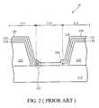
- FIG. 2is a cross-section of the display region 18 along a line A-A′ in FIG. 1 .
- the transflective display panel 10comprises a substrate 112 defined with the transmissive area 114 and the reflective area 115 thereon.
- an inter-layer dielectric (ILD) layer or a planarization layer 116can be disposed on the substrate 112 to protect electric devices, such as the thin film transistor located in the switch region 16 , on the substrate 112 .
- a transmissive hole 118is formed on the substrate 112 to expose the transmissive area 114 .
- a transparent electrode layer and a reflective layercan be formed in different sequences.
- a structurecan be formed with the transparent electrode layer on top or with the reflective layer on top. Since the reflective layer and the transparent electrode layer have different work function, the structure with the reflective layer on top can produce flicker problems, therefore the structure with transparent electrode on top is used as it can provide work function identical, thereby avoiding flicker problems.
- an adhesion layer 120 and a reflective layer 122are formed on the planarization layer 116 in sequence. Thereafter, a transparent electrode layer 126 is formed on the reflective layer 122 . As previously described, the reflective layer 122 can reflect ambient light to render images. The adhesion layer 120 improves a bonding force between the planarization layer 116 and the reflective layer 122 .
- An etching processcan be performed to pattern the reflective layer 122 and the adhesion layer 120 in the bottom of the transmissive hole 118 to expose the transmissive area 114 prior to formation of the transparent electrode layer 126 .
- the light source from the backlight unitcan transmit through the transmissive area 114 .
- the reflective layer 122is an aluminum alloy and the adhesion layer 120 includes molybdenum (Mo).
- Momolybdenum
- the adhesion layer 120has a larger etching rate than the reflective layer 122 due to material properties. This can result in an undercut phenomenon, shown for example as 123 in FIG. 2 , to be present in an edge 124 of the adhesion layer 120 adjacent to the transmissive area 114 . This can reduce step-coverage of the transparent electrode layer 126 and lead to the presence of a discontinuity region or a weak contact region when the transparent electrode layer 126 is formed thereon. Further, this can deteriorate the display performance of the transflective display panel 10 . Thus, a new transflective display panel structure and a fabricating method thereof are desirable.
- a substrate with a transmissive area thereonis first provided.
- a planarization layeris deposited on the substrate and a hole is then formed in the planarization layer to expose the transmissive area.
- a first reflective layer and a second reflective layerare formed on the planarization layer in sequence.
- an etching processis performed to pattern the first reflective layer and the second reflective layer to expose the transmissive area.
- the etching processhas a first etching rate to the first reflective layer and a second etching rate to the second reflective layer, which is larger than the first etching rate.
- a transparent electrode layeris then formed on the second reflective layer and the transmissive area.
- An embodiment of a transflective display panelcomprises a substrate with a transmissive area defined thereon and a planarization layer disposed on the substrate.
- the planarization layerhas a transmissive hole located on the transmissive area to expose the transmissive area.
- the transflective display panelfurther comprises a first reflective layer disposed on the planarization layer with a first opening and a second reflective layer disposed on the first reflective layer with a second opening.
- the second openingis disposed above the first opening and larger than the first opening.
- the first reflective layerhas a better anti-etching ability than the second reflective layer.
- FIG. 1is a schematic diagram of a conventional transflective display panel
- FIG. 2is a cross-section of the display region along a line A-A′ in FIG. 1 ;
- FIG. 3-5are schematic diagrams of an embodiment of a method of fabricating a transflective display panel
- FIG. 6is a schematic diagram of an embodiment of a transflective display panel
- FIG. 7is a schematic diagram of an embodiment of an LCD device.
- FIG. 8is a schematic diagram of an embodiment of an electronic device.
- Transflective display panelsaccording to various embodiments are provided. As will be described herein, some embodiments of the reflective layer structures are disposed on a planarization layer of a transflective display panel.
- FIG. 3-5are schematic diagrams according to various embodiments for fabricating a transflective display panel 210 .
- the transflective display panelcan comprise a substrate 212 with a transmissive area 214 and a reflective area 215 thereon.
- a planarization layer 216can be formed on the substrate 212 and then patterned to form a transmissive hole 218 to expose the transmissive area 214 and a part of the reflective area 215 .
- the substrate 212can comprise a glass substrate, a silicon substrate, a silicon on insulator substrate, a sapphire substrate, a polymer substrate, or any other suitable material.
- planarization layer 216can have a thickness of from about 2.9 to about 3.9 micrometers. Further, planarization layer 216 can comprise a dielectric material, such as silicon oxide, silicon nitride, polymer, or a combination thereof.
- a first reflective layer 220 and a second reflective layer 222can be formed on the transmissive area 214 , the reflective area 215 , and on sidewalls of the planarization layer 216 in the transmissive hole 218 .
- the first reflective layer 220can have a different etch rate than the second reflective layer 222 .
- the composition of first reflective layer 220 and second reflective layer 222can comprise the same or different material.
- first reflective layer 220 and second reflective layer 222can be formed of the same material but with different densities.
- first reflective layer 220 and second reflective layer 222can be formed by a sputtering process with different operating powers. For example, greater operating power can be used during fabricating the first reflective layer 222 so the first reflective layer 220 has a relatively porous structure and also a lower anti-etching ability, which can include a slower etching rate.
- an etching processis performed to pattern the first reflective layer 220 and the second reflective layer 222 in the transmissive area 214 .
- the etching processforms a first opening 230 in the first reflective layer 220 and a second opening 232 , which is disposed above the first opening 230 , in the second reflective layer 222 to expose the transmissive area 214 .
- the etching rate of the first reflective layer 220is relatively lower, such as 50 to 90% of that of the second reflective layer 222 , depends on many factors such as type of films, etching chemicals and etching conditions, etc.
- the second opening 232can be formed to be larger than the first opening 232 .
- edges of the patterned first reflective layer 220 and the patterned second reflective layer 222 in the bottom of the transmissive hole 218also form a tapered structure 234 with a tapered angle less than 70 degree to improve reliability in subsequent processes.
- a tapered structure 234 with a tapered angleis less than 60 degree.
- the first reflective layer 220has a thickness of about 1000 to 2000 angstroms and comprises aluminum neodymium (AlNd), aluminum (Al), silver (Ag), aluminum alloy, or combinations thereof.
- the second reflective layer 222has a thickness of about 100 to 800 angstroms and comprises aluminum neodymium (AlNd), aluminum (Al), silver (Ag), aluminum alloy, or a combination thereof.
- the etching processcan be performed at a temperature of about 40° C. Further, the etching process can be performed using an etching agent comprising 1-5% nitric acid, 70-80% phosphoric acid, and 5-15% acetic acid.
- the etching rate of the first reflective layer 220can be about 4000 to 5000 angstroms per minute, and the etching rate of the second reflective layer 222 can be about 5000 to 6000 angstroms per minute.
- a transparent electrode layer 226can then be deposited on the second reflective layer 222 and the transmissive area 214 through the first opening 230 and the second opening 232 .
- the transparent electrode layer 226can comprise indium tin oxide (ITO), indium zinc oxide (IZO), other acceptable materials, or combinations thereof.
- FIG. 6is a schematic diagram of an embodiment of a transflective display panel 310 .
- the transflective display panel 310has a similar structure and fabrication process and further comprises an additional adhesion layer 328 .
- the display panel 310comprises a substrate 312 with a reflective area 315 and a transmissive area 314 and a planarization layer 316 disposed on the substrate 312 .
- the planarization layer 316has a transmissive hole for exposing the transmissive area 314 on the surface of the substrate 312 .
- An adhesion layer 328 , a first reflective layer 320 , and a second reflective layer 322can be formed on the substrate 312 and the planarization layer 316 .
- An etching processcan then be performed to pattern the adhesion layer 328 , the first reflective layer 320 , and the second reflective layer 322 .
- the first reflective layer 320can have a better anti-etching ability than the second reflective layer 322 so the second opening 334 can be larger than the first opening 332 and a tapered structure can be formed. It results in potential improvement of a transparent electrode layer 326 formation in a sequent process.
- the adhesion layer 228can comprise molybdenum (Mo), titanium (Ti), other suitable materials, or combinations thereof and can have a thickness of about 50 to 300 angstroms.
- an LCD devicecan comprise the previously mentioned transflective display panel 210 or 310 .
- FIG. 7is a schematic diagram illustrating an LCD device 3 comprising an LCD panel 1 , such as the previously mentioned display panel 210 or 310 .
- the LCD device 3can further comprise a controller 2 coupled to the display panel 1 .
- the controller 2can comprise a driving circuit (not shown) to control the display panel 1 to render images in accordance with an input.
- FIG. 8is a schematic diagram illustrating an electronic device 5 incorporating the LCD device 3 shown in FIG. 7 .
- An input device 4can be coupled to the controller 2 of the LCD device 3 such as that shown in FIG. 5 or FIG. 6 to form an electronic device 5 .
- the input device 4can include a processor or the like to input data to the controller 2 to render images.
- the electronic device 5can be a portable device such as a PDA, notebook computer, tablet computer, cellular phone, or a display monitor device, or non-portable device such as a desktop computer.
- the two reflective layerscan have different anti-etching properties to form a tapered structure with a small tapered angle.
- disconnect or weak contact problems occurring in sequent fabrication processes for the transparent electrode layercan be potentially eliminated.
- reliability and stability of the transflective display panelscan be potentially improved.
Landscapes
- Physics & Mathematics (AREA)
- Nonlinear Science (AREA)
- Mathematical Physics (AREA)
- Chemical & Material Sciences (AREA)
- Crystallography & Structural Chemistry (AREA)
- General Physics & Mathematics (AREA)
- Optics & Photonics (AREA)
- Liquid Crystal (AREA)
- Devices For Indicating Variable Information By Combining Individual Elements (AREA)
Abstract
Description
- The invention relates to display panels, and more particularly, to transflective display (LCD) panels with reflective layer structures.
- As manufacturing costs decrease and quality improves, liquid crystal displays are increasingly employed in different products such as notebook computers, personal digital assistants (PDAs), mobile phones, clocks, and the like. Liquid crystal displays are passive luminous devices and can include a backlight unit for LCD devices.
- Typically, LCD devices can be divided into several types according to their display methods. Some examples are reflective LCD devices, transmissive LCD devices, and transflective LCD devices. A reflective LCD device saves power and reduces manufacturing costs by reflecting light from the environment to display images. A transmissive LCD device comprises an LCD panel and an additional backlight unit for providing a light source to the LCD panel, leading to higher brightness and less restrictions on use. Additionally, a transflective LCD device, which combines features of the transmissive LCD device and the reflective LCD device, is used because it can reflect ambient light to render images. The transmissive LCD device can also use a backlight unit to actively generate light in a low light environment, such as indoors or at night.
FIG. 1 is a schematic diagram of a conventionaltransflective display panel 10. As shown inFIG. 1 , thetransflective display panel 10 comprises a substrate with a plurality of scan lines12 arranged in a transverse direction, a plurality ofdata lines 14 arranged in a longitudinal direction perpendicular to the scan lines12, and a plurality of pixels corresponding to an intersection of each scan line12 anddata line 14. Each pixel comprises aswitch region 16 and adisplay region 18. In thetransflective display panel 10, theswitch region 16 comprises a thin film transistor, such as a polysilicon thin film transistor. Thedisplay region 18 can be covered by a reflective layer with a transmitting hole that forms atransmissive area 114 and areflective area 115. Thus, ambient light can be reflected by the reflective layer to a display image. A backlight unit can provide an additional light source through thetransmissive area 114 to assist image display in a low light environment.FIG. 2 is a cross-section of thedisplay region 18 along a line A-A′ inFIG. 1 . As shown inFIG. 2 , thetransflective display panel 10 comprises asubstrate 112 defined with thetransmissive area 114 and thereflective area 115 thereon. In conventional fabricating processes for TFT display panels, an inter-layer dielectric (ILD) layer or aplanarization layer 116 can be disposed on thesubstrate 112 to protect electric devices, such as the thin film transistor located in theswitch region 16, on thesubstrate 112. Atransmissive hole 118 is formed on thesubstrate 112 to expose thetransmissive area 114.- According to conventional fabricating processes of transflective display panels, a transparent electrode layer and a reflective layer can be formed in different sequences. For example, a structure can be formed with the transparent electrode layer on top or with the reflective layer on top. Since the reflective layer and the transparent electrode layer have different work function, the structure with the reflective layer on top can produce flicker problems, therefore the structure with transparent electrode on top is used as it can provide work function identical, thereby avoiding flicker problems.
- As shown in
FIG. 2 , anadhesion layer 120 and areflective layer 122 are formed on theplanarization layer 116 in sequence. Thereafter, atransparent electrode layer 126 is formed on thereflective layer 122. As previously described, thereflective layer 122 can reflect ambient light to render images. Theadhesion layer 120 improves a bonding force between theplanarization layer 116 and thereflective layer 122. - An etching process can be performed to pattern the
reflective layer 122 and theadhesion layer 120 in the bottom of thetransmissive hole 118 to expose thetransmissive area 114 prior to formation of thetransparent electrode layer 126. Thus, the light source from the backlight unit can transmit through thetransmissive area 114. - Typically, the
reflective layer 122 is an aluminum alloy and theadhesion layer 120 includes molybdenum (Mo). In the previously described etching process, theadhesion layer 120 has a larger etching rate than thereflective layer 122 due to material properties. This can result in an undercut phenomenon, shown for example as123 inFIG. 2 , to be present in anedge 124 of theadhesion layer 120 adjacent to thetransmissive area 114. This can reduce step-coverage of thetransparent electrode layer 126 and lead to the presence of a discontinuity region or a weak contact region when thetransparent electrode layer 126 is formed thereon. Further, this can deteriorate the display performance of thetransflective display panel 10. Thus, a new transflective display panel structure and a fabricating method thereof are desirable. - In an exemplary embodiment of a method of fabricating a transflective display panel, a substrate with a transmissive area thereon is first provided. A planarization layer is deposited on the substrate and a hole is then formed in the planarization layer to expose the transmissive area. A first reflective layer and a second reflective layer are formed on the planarization layer in sequence. Thereafter, an etching process is performed to pattern the first reflective layer and the second reflective layer to expose the transmissive area. The etching process has a first etching rate to the first reflective layer and a second etching rate to the second reflective layer, which is larger than the first etching rate. A transparent electrode layer is then formed on the second reflective layer and the transmissive area.
- An embodiment of a transflective display panel comprises a substrate with a transmissive area defined thereon and a planarization layer disposed on the substrate. The planarization layer has a transmissive hole located on the transmissive area to expose the transmissive area. The transflective display panel further comprises a first reflective layer disposed on the planarization layer with a first opening and a second reflective layer disposed on the first reflective layer with a second opening. The second opening is disposed above the first opening and larger than the first opening. The first reflective layer has a better anti-etching ability than the second reflective layer.
- The transflective display panel can be more fully understood by reading the subsequent detailed description and examples with references made to the accompanying drawings, wherein:
FIG. 1 is a schematic diagram of a conventional transflective display panel;FIG. 2 is a cross-section of the display region along a line A-A′ inFIG. 1 ;FIG. 3-5 are schematic diagrams of an embodiment of a method of fabricating a transflective display panel;FIG. 6 is a schematic diagram of an embodiment of a transflective display panel;FIG. 7 is a schematic diagram of an embodiment of an LCD device; andFIG. 8 is a schematic diagram of an embodiment of an electronic device.- Transflective display panels according to various embodiments are provided. As will be described herein, some embodiments of the reflective layer structures are disposed on a planarization layer of a transflective display panel.
FIG. 3-5 are schematic diagrams according to various embodiments for fabricating atransflective display panel 210. As shown inFIG. 3 , the transflective display panel can comprise asubstrate 212 with atransmissive area 214 and areflective area 215 thereon. Aplanarization layer 216 can be formed on thesubstrate 212 and then patterned to form atransmissive hole 218 to expose thetransmissive area 214 and a part of thereflective area 215. In an embodiment, thesubstrate 212 can comprise a glass substrate, a silicon substrate, a silicon on insulator substrate, a sapphire substrate, a polymer substrate, or any other suitable material. According to various embodiments,planarization layer 216 can have a thickness of from about 2.9 to about 3.9 micrometers. Further,planarization layer 216 can comprise a dielectric material, such as silicon oxide, silicon nitride, polymer, or a combination thereof.- As shown in
FIG. 4 , a firstreflective layer 220 and a secondreflective layer 222 can be formed on thetransmissive area 214, thereflective area 215, and on sidewalls of theplanarization layer 216 in thetransmissive hole 218. - According to various embodiments, the first
reflective layer 220 can have a different etch rate than the secondreflective layer 222. According to various embodiments, the composition of firstreflective layer 220 and secondreflective layer 222 can comprise the same or different material. Further, according to various embodiments, firstreflective layer 220 and secondreflective layer 222 can be formed of the same material but with different densities. In an embodiment of thetransflective display panel 210, firstreflective layer 220 and secondreflective layer 222 can be formed by a sputtering process with different operating powers. For example, greater operating power can be used during fabricating the firstreflective layer 222 so the firstreflective layer 220 has a relatively porous structure and also a lower anti-etching ability, which can include a slower etching rate. - Thereafter, an etching process is performed to pattern the first
reflective layer 220 and the secondreflective layer 222 in thetransmissive area 214. The etching process forms afirst opening 230 in the firstreflective layer 220 and asecond opening 232, which is disposed above thefirst opening 230, in the secondreflective layer 222 to expose thetransmissive area 214. Since the firstreflective layer 220 has better anti-etching ability and higher densities, the etching rate of the firstreflective layer 220 is relatively lower, such as 50 to 90% of that of the secondreflective layer 222, depends on many factors such as type of films, etching chemicals and etching conditions, etc. Thus, thesecond opening 232 can be formed to be larger than thefirst opening 232. The edges of the patterned firstreflective layer 220 and the patterned secondreflective layer 222 in the bottom of thetransmissive hole 218 also form atapered structure 234 with a tapered angle less than 70 degree to improve reliability in subsequent processes. According to various embodiments, atapered structure 234 with a tapered angle is less than 60 degree. - In an embodiment of the
transflective display device 210, the firstreflective layer 220 has a thickness of about 1000 to 2000 angstroms and comprises aluminum neodymium (AlNd), aluminum (Al), silver (Ag), aluminum alloy, or combinations thereof. The secondreflective layer 222 has a thickness of about 100 to 800 angstroms and comprises aluminum neodymium (AlNd), aluminum (Al), silver (Ag), aluminum alloy, or a combination thereof. - According to various embodiments, the etching process can be performed at a temperature of about 40° C. Further, the etching process can be performed using an etching agent comprising 1-5% nitric acid, 70-80% phosphoric acid, and 5-15% acetic acid. The etching rate of the first
reflective layer 220 can be about 4000 to 5000 angstroms per minute, and the etching rate of the secondreflective layer 222 can be about 5000 to 6000 angstroms per minute. - As shown in
FIG. 5 , atransparent electrode layer 226 can then be deposited on the secondreflective layer 222 and thetransmissive area 214 through thefirst opening 230 and thesecond opening 232. In an embodiment of thetransflective display panel 210, thetransparent electrode layer 226 can comprise indium tin oxide (ITO), indium zinc oxide (IZO), other acceptable materials, or combinations thereof. FIG. 6 is a schematic diagram of an embodiment of atransflective display panel 310. In comparison with thetransflective display panel 210, thetransflective display panel 310 has a similar structure and fabrication process and further comprises anadditional adhesion layer 328. As shown inFIG. 6 , thedisplay panel 310 comprises asubstrate 312 with areflective area 315 and atransmissive area 314 and aplanarization layer 316 disposed on thesubstrate 312. Theplanarization layer 316 has a transmissive hole for exposing thetransmissive area 314 on the surface of thesubstrate 312. Anadhesion layer 328, a firstreflective layer 320, and a secondreflective layer 322 can be formed on thesubstrate 312 and theplanarization layer 316. An etching process can then be performed to pattern theadhesion layer 328, the firstreflective layer 320, and the secondreflective layer 322. As previously described, the firstreflective layer 320 can have a better anti-etching ability than the secondreflective layer 322 so the second opening334 can be larger than the first opening332 and a tapered structure can be formed. It results in potential improvement of atransparent electrode layer 326 formation in a sequent process. In an embodiment of thetransflective display panel 310, the adhesion layer228 can comprise molybdenum (Mo), titanium (Ti), other suitable materials, or combinations thereof and can have a thickness of about 50 to 300 angstroms.- According to various embodiments an LCD device can comprise the previously mentioned
transflective display panel FIG. 7 is a schematic diagram illustrating anLCD device 3 comprising anLCD panel 1, such as the previously mentioneddisplay panel LCD device 3 can further comprise acontroller 2 coupled to thedisplay panel 1. Thecontroller 2 can comprise a driving circuit (not shown) to control thedisplay panel 1 to render images in accordance with an input. FIG. 8 is a schematic diagram illustrating anelectronic device 5 incorporating theLCD device 3 shown inFIG. 7 . Aninput device 4 can be coupled to thecontroller 2 of theLCD device 3 such as that shown inFIG. 5 orFIG. 6 to form anelectronic device 5. Theinput device 4 can include a processor or the like to input data to thecontroller 2 to render images. Theelectronic device 5 can be a portable device such as a PDA, notebook computer, tablet computer, cellular phone, or a display monitor device, or non-portable device such as a desktop computer.- When compared with the conventional transflective display panel with only one reflective layer, embodiments layers. Further, the two reflective layers can have different anti-etching properties to form a tapered structure with a small tapered angle. Thus, disconnect or weak contact problems occurring in sequent fabrication processes for the transparent electrode layer can be potentially eliminated. Thus, reliability and stability of the transflective display panels can be potentially improved.
- While the invention has been described by way of example and in terms of various embodiments, it is to be understood that the invention is not limited thereto.
Claims (25)
Priority Applications (4)
| Application Number | Priority Date | Filing Date | Title |
|---|---|---|---|
| US11/110,846US7248317B2 (en) | 2005-04-21 | 2005-04-21 | Transflective display panels and methods for making the same |
| TW094138401ATWI320117B (en) | 2005-04-21 | 2005-11-02 | Transflective display panels and methods for making the same |
| CNB2005101247229ACN100375918C (en) | 2005-04-21 | 2005-11-16 | Semi-transmission semi-reflection type liquid crystal display panel and manufacturing method thereof |
| JP2006105209AJP4578430B2 (en) | 2005-04-21 | 2006-04-06 | Transflective display panel and manufacturing method thereof |
Applications Claiming Priority (1)
| Application Number | Priority Date | Filing Date | Title |
|---|---|---|---|
| US11/110,846US7248317B2 (en) | 2005-04-21 | 2005-04-21 | Transflective display panels and methods for making the same |
Publications (2)
| Publication Number | Publication Date |
|---|---|
| US20060238676A1true US20060238676A1 (en) | 2006-10-26 |
| US7248317B2 US7248317B2 (en) | 2007-07-24 |
Family
ID=37186468
Family Applications (1)
| Application Number | Title | Priority Date | Filing Date |
|---|---|---|---|
| US11/110,846Expired - Fee RelatedUS7248317B2 (en) | 2005-04-21 | 2005-04-21 | Transflective display panels and methods for making the same |
Country Status (4)
| Country | Link |
|---|---|
| US (1) | US7248317B2 (en) |
| JP (1) | JP4578430B2 (en) |
| CN (1) | CN100375918C (en) |
| TW (1) | TWI320117B (en) |
Cited By (5)
| Publication number | Priority date | Publication date | Assignee | Title |
|---|---|---|---|---|
| US20080094534A1 (en)* | 2004-06-05 | 2008-04-24 | Lg Philips Lcd Co., Ltd. | Liquid crystal display device and fabricating method thereof |
| US20090185119A1 (en)* | 2006-05-01 | 2009-07-23 | Sharp Kabushiki Kaisha | Liquid crystal display and method for manufacturing liquid crystal display |
| US20090195740A1 (en)* | 2006-05-01 | 2009-08-06 | Sharp Kabushiki Kaisha | Liquid crystal display device and method of manufacturing liquid crystal display device |
| US20100020278A1 (en)* | 2007-03-15 | 2010-01-28 | Tetsuo Fujita | Liquid crystal display device and production method thereof |
| US20150116623A1 (en)* | 2013-10-31 | 2015-04-30 | Japan Display Inc. | Liquid crystal display device |
Families Citing this family (8)
| Publication number | Priority date | Publication date | Assignee | Title |
|---|---|---|---|---|
| EP2034570A1 (en)* | 2003-07-03 | 2009-03-11 | PD-LD, Inc. | Use of volume bragg gratings for the conditioning of laser emission characteristics |
| JP2005260379A (en)* | 2004-03-09 | 2005-09-22 | Nec Corp | Digital broadcasting system |
| KR101733128B1 (en)* | 2010-04-26 | 2017-05-08 | 삼성디스플레이 주식회사 | Thin film transistor substrate for transflective liquid crystal display device and manufacturing method of the same |
| CN102621753B (en)* | 2011-01-28 | 2015-02-18 | 联胜(中国)科技有限公司 | Pixel structure and display panel |
| TWM415322U (en) | 2011-04-01 | 2011-11-01 | Chunghwa Picture Tubes Ltd | Liquid crystal panel |
| US9134529B2 (en) | 2011-07-21 | 2015-09-15 | Pixronix, Inc. | Display device with tapered light reflecting layer and manufacturing method for same |
| CN108666350A (en)* | 2014-02-11 | 2018-10-16 | 群创光电股份有限公司 | display panel |
| CN107731854B (en)* | 2017-09-28 | 2020-05-05 | 京东方科技集团股份有限公司 | Method for preparing an array substrate, array substrate, and display device |
Citations (3)
| Publication number | Priority date | Publication date | Assignee | Title |
|---|---|---|---|---|
| US20040252262A1 (en)* | 2003-06-10 | 2004-12-16 | Lg. Philips Lcd Co., Ltd. | Transflective liquid crystal display device |
| US20050140868A1 (en)* | 2003-12-26 | 2005-06-30 | Han-Wook Hwang | Array substrate for a transflective liquid crystal display device and fabricating method thereof |
| US20050168671A1 (en)* | 2004-02-04 | 2005-08-04 | Lee Jeong H. | Transflective liquid crystal display device and method for manufacturing the same |
Family Cites Families (10)
| Publication number | Priority date | Publication date | Assignee | Title |
|---|---|---|---|---|
| JP2002202502A (en)* | 2000-03-31 | 2002-07-19 | Matsushita Electric Ind Co Ltd | Shaped body, reflector, reflective display element, and method of manufacturing reflector |
| JP3908552B2 (en)* | 2001-03-29 | 2007-04-25 | Nec液晶テクノロジー株式会社 | Liquid crystal display device and manufacturing method thereof |
| JP3808356B2 (en)* | 2001-12-04 | 2006-08-09 | 株式会社日立製作所 | Liquid crystal display |
| KR100467944B1 (en)* | 2002-07-15 | 2005-01-24 | 엘지.필립스 엘시디 주식회사 | Transflective Liquid Crystal Display Device and Method for fabricating the same |
| JP4110885B2 (en)* | 2002-08-27 | 2008-07-02 | セイコーエプソン株式会社 | LIQUID CRYSTAL DISPLAY DEVICE, ITS MANUFACTURING METHOD, AND ELECTRONIC DEVICE |
| JP4214748B2 (en)* | 2002-09-20 | 2009-01-28 | セイコーエプソン株式会社 | Liquid crystal display device and electronic device |
| JP4262582B2 (en)* | 2002-11-27 | 2009-05-13 | シャープ株式会社 | Method for forming conductive element and method for forming reflective electrode part of liquid crystal display device |
| KR100494455B1 (en)* | 2003-06-11 | 2005-06-10 | 엘지.필립스 엘시디 주식회사 | An array substrate for transflective LCD and method for fabricating of the same |
| JP4085094B2 (en)* | 2004-02-19 | 2008-04-30 | シャープ株式会社 | Manufacturing method of conductive element substrate, manufacturing method of liquid crystal display device |
| JP2005277402A (en)* | 2004-02-25 | 2005-10-06 | Mitsubishi Gas Chem Co Inc | Etching composition for laminated film including reflective electrode film and method for forming laminated wiring structure |
- 2005
- 2005-04-21USUS11/110,846patent/US7248317B2/ennot_activeExpired - Fee Related
- 2005-11-02TWTW094138401Apatent/TWI320117B/ennot_activeIP Right Cessation
- 2005-11-16CNCNB2005101247229Apatent/CN100375918C/ennot_activeExpired - Fee Related
- 2006
- 2006-04-06JPJP2006105209Apatent/JP4578430B2/ennot_activeExpired - Fee Related
Patent Citations (3)
| Publication number | Priority date | Publication date | Assignee | Title |
|---|---|---|---|---|
| US20040252262A1 (en)* | 2003-06-10 | 2004-12-16 | Lg. Philips Lcd Co., Ltd. | Transflective liquid crystal display device |
| US20050140868A1 (en)* | 2003-12-26 | 2005-06-30 | Han-Wook Hwang | Array substrate for a transflective liquid crystal display device and fabricating method thereof |
| US20050168671A1 (en)* | 2004-02-04 | 2005-08-04 | Lee Jeong H. | Transflective liquid crystal display device and method for manufacturing the same |
Cited By (30)
| Publication number | Priority date | Publication date | Assignee | Title |
|---|---|---|---|---|
| US20080094534A1 (en)* | 2004-06-05 | 2008-04-24 | Lg Philips Lcd Co., Ltd. | Liquid crystal display device and fabricating method thereof |
| US8115893B2 (en)* | 2004-06-05 | 2012-02-14 | Lg Display Co., Ltd. | Liquid crystal display device with reflection and transmission regions |
| US20090185119A1 (en)* | 2006-05-01 | 2009-07-23 | Sharp Kabushiki Kaisha | Liquid crystal display and method for manufacturing liquid crystal display |
| US20090195740A1 (en)* | 2006-05-01 | 2009-08-06 | Sharp Kabushiki Kaisha | Liquid crystal display device and method of manufacturing liquid crystal display device |
| US8294854B2 (en)* | 2006-05-01 | 2012-10-23 | Sharp Kabushiki Kaisha | Liquid crystal display comprising a reflection region having first, second and third recesses and method for manufacturing the same |
| US8300186B2 (en)* | 2006-05-01 | 2012-10-30 | Sharp Kabushiki Kaisha | Liquid crystal display device comprising a reflection region having tilted first and second recesses and method for manufacturing the same |
| US20100020278A1 (en)* | 2007-03-15 | 2010-01-28 | Tetsuo Fujita | Liquid crystal display device and production method thereof |
| US9921440B2 (en)* | 2013-10-31 | 2018-03-20 | Japan Display Inc. | Liquid crystal display device |
| US10247990B2 (en)* | 2013-10-31 | 2019-04-02 | Japan Display Inc. | Liquid crystal display device |
| US20160109771A1 (en)* | 2013-10-31 | 2016-04-21 | Japan Display Inc. | Liquid crystal display device |
| US9417496B2 (en)* | 2013-10-31 | 2016-08-16 | Japan Display Inc. | Liquid crystal display device |
| US9575385B2 (en)* | 2013-10-31 | 2017-02-21 | Japan Display Inc. | Liquid crystal display device |
| US20170146872A1 (en)* | 2013-10-31 | 2017-05-25 | Japan Display Inc. | Liquid crystal display device |
| US9778520B2 (en)* | 2013-10-31 | 2017-10-03 | Japan Display Inc. | Liquid crystal display device |
| US20150116623A1 (en)* | 2013-10-31 | 2015-04-30 | Japan Display Inc. | Liquid crystal display device |
| US20180164648A1 (en)* | 2013-10-31 | 2018-06-14 | Japan Display Inc. | Liquid crystal display device |
| US10031383B2 (en)* | 2013-10-31 | 2018-07-24 | Japan Display Inc. | Liquid crystal display device |
| US10126611B2 (en)* | 2013-10-31 | 2018-11-13 | Japan Display Inc. | Liquid crystal display device |
| US9250491B2 (en)* | 2013-10-31 | 2016-02-02 | Japan Display Inc. | Liquid crystal display device |
| US10877325B2 (en)* | 2013-10-31 | 2020-12-29 | Japan Display Inc. | Liquid crystal display device |
| US11150523B2 (en)* | 2013-10-31 | 2021-10-19 | Japan Display Inc. | Liquid crystal display device |
| US11480833B2 (en)* | 2013-10-31 | 2022-10-25 | Japan Display Inc. | Liquid crystal display device |
| US20230020723A1 (en)* | 2013-10-31 | 2023-01-19 | Japan Display Inc. | Liquid crystal display device |
| US11668982B2 (en)* | 2013-10-31 | 2023-06-06 | Japan Display Inc. | Liquid crystal display device |
| US20230288759A1 (en)* | 2013-10-31 | 2023-09-14 | Japan Display Inc. | Liquid crystal display device |
| US11906857B2 (en)* | 2013-10-31 | 2024-02-20 | Japan Display Inc. | Liquid crystal display device |
| US20240142830A1 (en)* | 2013-10-31 | 2024-05-02 | Japan Display Inc. | Liquid crystal display device |
| US12092932B2 (en)* | 2013-10-31 | 2024-09-17 | Japan Display Inc. | Liquid crystal display device |
| US20240393645A1 (en)* | 2013-10-31 | 2024-11-28 | Japan Display Inc. | Liquid crystal display device |
| US12282235B2 (en)* | 2013-10-31 | 2025-04-22 | Japan Display Inc. | Liquid crystal display device |
Also Published As
| Publication number | Publication date |
|---|---|
| CN100375918C (en) | 2008-03-19 |
| TW200638110A (en) | 2006-11-01 |
| CN1854838A (en) | 2006-11-01 |
| JP2006301625A (en) | 2006-11-02 |
| US7248317B2 (en) | 2007-07-24 |
| TWI320117B (en) | 2010-02-01 |
| JP4578430B2 (en) | 2010-11-10 |
Similar Documents
| Publication | Publication Date | Title |
|---|---|---|
| JP4578430B2 (en) | Transflective display panel and manufacturing method thereof | |
| CN1442741B (en) | Liquid crystal display device having a plurality of pixel electrodes | |
| CN113359344B (en) | Array substrate, liquid crystal display panel and liquid crystal display device | |
| US20170200750A1 (en) | Method for manufacturing array substrate | |
| US8845343B2 (en) | Array substrate for reflective type or transflective type liquid crystal display device | |
| US7956963B2 (en) | Pixel structure for transflective LCD panel having a reflective structure formed in a depression on the TFT substrate | |
| US20170263734A1 (en) | Thin film transistor (tft) array substrate and fabrication method thereof, and display device | |
| JP2004145332A (en) | Structure of liquid crystal display of dual display | |
| TW201042324A (en) | System for displaying images | |
| US10551696B2 (en) | Method of producing metal electrode, array substrate and method of producing the same, display device | |
| CN111722445A (en) | Array substrate, liquid crystal display panel and display device | |
| JP2007156442A (en) | Laminated storage capacitor structure used for low-temperature polysilicon thin film transistor liquid crystal display device | |
| US7442567B2 (en) | Method for fabricating transflective liquid crystal display | |
| US10128272B2 (en) | Thin film transistor array substrate, method for fabricating the same and display device | |
| US8125595B2 (en) | Metal material and its manufacturing method, thin-film device and its manufacturing method, element-side substrate and its manufacturing method, and liquid crystal display and its manufacturing method | |
| KR100719333B1 (en) | Reflective-transmissive thin film transistor liquid crystal display device and manufacturing method thereof | |
| JP2003255375A (en) | Liquid crystal display | |
| CN1282894C (en) | Dual-sided LCD monitor | |
| KR20080003085A (en) | Transverse electric field mode liquid crystal display device and manufacturing method thereof | |
| US7342253B2 (en) | Display panels with anti-Newton ring structures | |
| CN101126855A (en) | Electronic device, transflective pixel structure of liquid crystal display panel and manufacturing method thereof | |
| CN1979315A (en) | image display system | |
| KR100848553B1 (en) | Manufacturing method of liquid crystal display device preventing damage of gate pad | |
| CN114326232A (en) | Array substrate, manufacturing method thereof, display panel and display device | |
| JP5436926B2 (en) | Semi-permeable membrane |
Legal Events
| Date | Code | Title | Description |
|---|---|---|---|
| AS | Assignment | Owner name:TOPPOLY OPTOELECTRONICS CORPORATION, TAIWAN Free format text:ASSIGNMENT OF ASSIGNORS INTEREST;ASSIGNORS:YANG, KUEN-SHIEN;SHIH, AN;LEE, TEHSIN;AND OTHERS;REEL/FRAME:016498/0818 Effective date:20050413 | |
| STCF | Information on status: patent grant | Free format text:PATENTED CASE | |
| AS | Assignment | Owner name:TPO DISPLAYS CORP., TAIWAN Free format text:CHANGE OF NAME;ASSIGNOR:TOPPOLY OPTOELECTRONICS CORPORATION;REEL/FRAME:019820/0990 Effective date:20060605 | |
| AS | Assignment | Owner name:TPO DISPLAYS CORP., TAIWAN Free format text:CHANGE OF NAME;ASSIGNOR:TOPPOLY OPTOELECTRONICS CORPORATION;REEL/FRAME:019992/0734 Effective date:20060605 Owner name:TPO DISPLAYS CORP.,TAIWAN Free format text:CHANGE OF NAME;ASSIGNOR:TOPPOLY OPTOELECTRONICS CORPORATION;REEL/FRAME:019992/0734 Effective date:20060605 | |
| FPAY | Fee payment | Year of fee payment:4 | |
| AS | Assignment | Owner name:INNOLUX CORPORATION, TAIWAN Free format text:CHANGE OF NAME;ASSIGNOR:CHIMEI INNOLUX CORPORATION;REEL/FRAME:032604/0487 Effective date:20121219 | |
| FPAY | Fee payment | Year of fee payment:8 | |
| FEPP | Fee payment procedure | Free format text:MAINTENANCE FEE REMINDER MAILED (ORIGINAL EVENT CODE: REM.); ENTITY STATUS OF PATENT OWNER: LARGE ENTITY | |
| LAPS | Lapse for failure to pay maintenance fees | Free format text:PATENT EXPIRED FOR FAILURE TO PAY MAINTENANCE FEES (ORIGINAL EVENT CODE: EXP.); ENTITY STATUS OF PATENT OWNER: LARGE ENTITY | |
| STCH | Information on status: patent discontinuation | Free format text:PATENT EXPIRED DUE TO NONPAYMENT OF MAINTENANCE FEES UNDER 37 CFR 1.362 | |
| FP | Expired due to failure to pay maintenance fee | Effective date:20190724 |