US20060238632A1 - Rolling shutter for prevention of blooming - Google Patents
Rolling shutter for prevention of bloomingDownload PDFInfo
- Publication number
- US20060238632A1 US20060238632A1US11/114,094US11409405AUS2006238632A1US 20060238632 A1US20060238632 A1US 20060238632A1US 11409405 AUS11409405 AUS 11409405AUS 2006238632 A1US2006238632 A1US 2006238632A1
- Authority
- US
- United States
- Prior art keywords
- rows
- row
- pixels
- hard reset
- pixel
- Prior art date
- Legal status (The legal status is an assumption and is not a legal conclusion. Google has not performed a legal analysis and makes no representation as to the accuracy of the status listed.)
- Granted
Links
- 238000005096rolling processMethods0.000titleclaimsabstractdescription27
- 230000002265preventionEffects0.000titledescription2
- 230000010354integrationEffects0.000claimsabstractdescription28
- 238000000034methodMethods0.000claimsabstractdescription18
- 238000003384imaging methodMethods0.000claimsdescription15
- 238000009792diffusion processMethods0.000description7
- 238000009825accumulationMethods0.000description6
- 230000000694effectsEffects0.000description4
- 239000000758substrateSubstances0.000description4
- 238000010586diagramMethods0.000description3
- 230000004044responseEffects0.000description3
- 230000006870functionEffects0.000description2
- 230000005055memory storageEffects0.000description2
- 230000003321amplificationEffects0.000description1
- 238000003491arrayMethods0.000description1
- 238000006243chemical reactionMethods0.000description1
- 230000005574cross-species transmissionEffects0.000description1
- 230000001186cumulative effectEffects0.000description1
- 238000001514detection methodMethods0.000description1
- 238000006073displacement reactionMethods0.000description1
- 238000005516engineering processMethods0.000description1
- 230000004048modificationEffects0.000description1
- 238000012986modificationMethods0.000description1
- 238000003199nucleic acid amplification methodMethods0.000description1
- 230000008569processEffects0.000description1
- 239000004065semiconductorSubstances0.000description1
- 230000006641stabilisationEffects0.000description1
- 238000011105stabilizationMethods0.000description1
- 238000006467substitution reactionMethods0.000description1
Images


Classifications
- H—ELECTRICITY
- H04—ELECTRIC COMMUNICATION TECHNIQUE
- H04N—PICTORIAL COMMUNICATION, e.g. TELEVISION
- H04N25/00—Circuitry of solid-state image sensors [SSIS]; Control thereof
- H04N25/50—Control of the SSIS exposure
- H04N25/53—Control of the integration time
- H04N25/531—Control of the integration time by controlling rolling shutters in CMOS SSIS
- H—ELECTRICITY
- H04—ELECTRIC COMMUNICATION TECHNIQUE
- H04N—PICTORIAL COMMUNICATION, e.g. TELEVISION
- H04N25/00—Circuitry of solid-state image sensors [SSIS]; Control thereof
- H04N25/60—Noise processing, e.g. detecting, correcting, reducing or removing noise
- H04N25/62—Detection or reduction of noise due to excess charges produced by the exposure, e.g. smear, blooming, ghost image, crosstalk or leakage between pixels
- H04N25/621—Detection or reduction of noise due to excess charges produced by the exposure, e.g. smear, blooming, ghost image, crosstalk or leakage between pixels for the control of blooming
Definitions
- the present inventionrelates to a rolling shutter for the prevention of blooming in a CMOS pixel cell array.
- Image sensorsare used in a variety of digital image capture systems, including products such as scanners, copiers, and digital cameras.
- the image sensoris typically composed of an array of light-sensitive pixel cells that are electrically responsive to incident light reflected from an object or scene whose image is to be captured.
- a CMOS imagerincludes a focal plane array of pixel cells, each cell includes a photosensor, for example, a photogate, photoconductor or a photodiode overlying a substrate for producing a photo-generated charge in a doped region of the substrate.
- the active elements of a pixel cellfor example a four transistor (4T) pixel cell, perform the necessary functions of (1) photon to charge conversion; (2) resetting a floating diffusion region to a known state; (3) transfer of charge to the floating diffusion region; (4) selection of a pixel cell for readout; and (5) output and amplification of a signal representing a reset voltage and a pixel signal voltage based on the photo-converted charges.
- the charge at the floating diffusion regionis converted to a pixel or reset output voltage by a source follower output transistor.
- CMOS imaging circuitsprocessing steps thereof, and detailed descriptions of the functions of various CMOS elements of an imaging circuit are described, for example, in U.S. Pat. Nos. 6,140,630, 6,376,868, 6,310,366, 6,326,652, 6,204,524, and 6,333,205, all assigned to Micron Technology, Inc. The disclosures of each of the forgoing patents are hereby incorporated by reference herein in their entirety.
- FIGS. 1AA conventional CMOS four-transistor (4T) pixel cell 10 is illustrated in FIGS. 1A .
- the illustrated cell 10includes a pinned photodiode 13 as a photosensor.
- the CMOS cell 10may include a photogate, photoconductor or other photon-to-charge converting device, in lieu of the pinned photodiode 13 , as the initial accumulating area for photo-generated charge.
- the photodiode 13includes a p+ surface accumulation layer and an underlying n- charge accumulation region formed in a p-type semiconductor substrate. In the exemplary pixel 10 , accumulated charges are accumulated electrons.
- the pixel cell 10has a transfer gate 7 , which is part of a transfer transistor 8 , for transferring photocharges generated in the n- accumulation region to a floating diffusion region 3 .
- the floating diffusion region 3is further connected to a gate 27 of a source follower transistor 28 .
- the source follower transistor 28provides an output signal to a row select transistor 38 having a gate 37 for selectively gating the output signal to a column line 50 .
- the column line 50is selected for readout by a column select transistor 52 , which applies a current source 54 to column line 50 .
- a reset transistor 18 having a gate 17resets the floating diffusion region 3 to a specified charge level by connecting it to a supply voltage V aa-pix before each charge transfer from the n- accumulation region of the photodiode 13 .
- FIG. 1Billustrates a block diagram of an exemplary CMOS imager 108 having a pixel array 140 comprising a plurality of pixel cells arranged in a predetermined number of columns and rows, with each pixel cell being constructed as illustrated and described above with respect to FIGS. 1A or using other known pixel architectures.
- Attached to the array 140is signal processing circuitry for controlling the pixel array 140 , as described herein, at least part of which may be formed in the substrate.
- the pixel cells of each row in array 140are all turned on at the same time by a row select line, and the pixel cells of each column are selectively output by respective column select lines.
- a plurality of TX, read, row select and column select linesare provided for the entire array 140 .
- the row linesare selectively activated by a row driver 145 in response to row address decoder 155 .
- the column select linesare selectively activated by a column driver 160 in response to column address decoder 170 .
- a row and column addressis provided for each pixel cell.
- the CMOS imager 108is operated by a timing and control circuit 150 , which controls address decoders 155 , 170 for selecting the appropriate row and column lines for pixel readout.
- the control circuit 150also controls the row and column driver circuitry 145 , 160 such that they apply driving voltages to the drive transistors of the selected row and column lines.
- the pixel column signalswhich typically include a pixel reset signal V rst and a pixel image signal V sig, are output to column driver 160 , on output lines, and are read by a sample and hold circuit 161 .
- V rstis read from a pixel cell 10 immediately after the floating diffusion region 3 is reset.
- V sigrepresents the amount of charges generated by the photosensitive element of the pixel cell 10 in response to applied light during an integration period.
- a differential signal(V rst ⁇ V sig ) is produced by differential amplifier 162 for each readout pixel cell.
- the differential signalis digitized by an analog-to-digital converter 175 (ADC).
- ADCanalog-to-digital converter 175 supplies the digitized pixel signals to an image processor 180 , which forms and outputs a digital image.
- Bloomingoccurs when a photodiode or other photosensitive device is overexposed, i.e., the photodiode 13 is exposed to more photons than it is capable of absorbing and converting to electrons. This is typically due to exposure of a pixel to an overly intense light source, or to exposing the pixel for too long a period of time. The excess electrons can spill over into pixels in nearby rows and columns. This overflow distorts the image, and can wash out portions of the image near the overexposed portion.
- a typical technique for exposing and reading out images using pixel array 140is by using a rolling shutter. That is, as row N is being read out, row N+X is hard reset, with X representing a number of rows further down in the array 140 .
- a hard resetmeans that both the reset transistors and transfer transistors are turned on to reset the photodiode, and when the transfer transistor is turned off, an integration period begins.
- the time difference between a hard reset of a row and its subsequent readoutis the pixel exposure time, also known as integration time.
- the rolling shutteroperated by control circuit 150 ( FIG. 1B ) includes a read row 200 and a hard reset row 201 .
- An overexposed pixel 210 and bloom region 211is also shown.
- the integration period X of the rolling shutteris the time it takes to sequentially read out 10 rows.
- the integration periodcan be set responsive to the amount of incident light and on the capacity of the photodiodes 13 in order to prevent individual pixels from overexposing and blooming during the integration period.
- hard reset row 201(at row 16 ) is hard reset, which then begins an integration period for row 16 where row 16 begins to collect photons until the read row 200 reaches row 16 .
- FIGS. 2B-2Fshow the row by row progression of read row 200 and hard reset row 201 , with the hard reset row 201 always 10 rows ahead of the read row 200 . Once rows 6 - 15 are read out in sequence, row 16 will then be read out, and so on. This conventional rolling shutter technique does not adequately compensate for blooming, however.
- Bloomingcan often affect pixels several rows or columns away from the initially overexposed pixel.
- the adjacent pixelswhich absorb a large portion of the deflected electrons from the initial overexposed pixel, can be overexposed themselves and begin to deflect electrons. Additionally, many electrons may be deflected to pixels several rows or columns away.
- an overexposed pixel 210 having a bloom region 211is shown.
- a single pixel 210is exposed to light of sufficient intensity to overload the photosensor charge accumulation region 14 (see FIG. 1A ) and send excess electrons as far away as five pixels in all directions.
- all pixels within the bloom region 211having a radius of approximately five pixels, will produce an inaccurate result because of the excess electrons from pixel 210 .
- the hard resetting of row 17will not prevent photon overflow to still integrating row 16 . Also, in situations where the light is particularly intense, or where the photon capacity of a pixel cell is particularly small, the portion of row 17 in the bloom region 211 may refill and overflow to row 16 in less time than it takes to integrate one row, further distorting the portion of row 16 in the bloom region 211 .
- FIGS. 2C-2Fshow the progression of the rolling shutter and its inability to fully compensate for blooming.
- the hard reset row 201must reach the overexposed pixel 210 (at row 21 ) to fully discharge the excess electrons by a hard reset, as shown in FIG. 2F .
- the hard reset row 201reaches the overexposed pixel 210 at row 21 , however, portions of rows 16 - 20 in the bloom region 211 will have already been distorted by the excess electrons which have been deflected from the pixel 210 before hard reset, as shown in FIGS. 2B-2E .
- overexposed pixel 210is hard reset and stops contributing to the distortion of bloom region 211 , the effects of the excess electrons in bloom region 211 will remain until the row is discharged, either by being hard reset for rows 22 +, or by being read out for rows 16 - 20 , distorting the portion of the image in that portion of the bloom region 211 .
- the present inventionemploys a rolling shutter technique having multiple hard reset rows that counteract the effects of blooming.
- the advantagesare twofold. First, as the shutter progresses row-by-row down the array, each row is hard reset multiple times before the integration period begins, thereby ensuring that the row is in a true hard reset condition at the beginning of the integration period. Second, multiple leading rows are hard reset at the beginning of the integration period for a given row, thereby making it less likely that overexposed pixels several rows away will be able to distort the given row.
- rows N+X, . . . N+X+(Y ⁇ 1)are all hard reset, with X representing the integration time, expressed in rows, of the pixel and Y representing the number of hard reset rows in the shutter.
- Ycan be as few as 2, and it is generally sufficient that Y be between 3 and 5.However, Y can be as large as the total number of rows in the array minus X (the number of rows needed to integrate the pixel result).
- the hard reset rowsmay be arranged as non-consecutive rows.
- FIG. 1Ais a schematic diagram of a conventional pixel cell
- FIG. 1Bdepicts a block diagram of an imager device which can employ the invention
- FIGS. 2A-2Fshow the operation of a conventional rolling shutter
- FIGS. 3A-3Dshow the operation of a rolling shutter according to the present invention
- FIG. 4shows a processor system incorporating at least one imager device constructed in accordance with an embodiment of the invention.
- FIG. 5shows the arrangement of a rolling shutter according to an alternate embodiment of the present invention.
- FIG. 6shows the arrangement of a rolling shutter according to another alternate embodiment of the present invention.
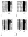
- FIGS. 3A-3Da portion of a CMOS pixel array 140 is shown.
- the array 140 , overexposed pixel 210 and bloom region 211have the same designations as discussed above with respect to FIGS. 2A-2F .
- a rolling shutter according to present invention, controlled by control circuit 150 ( FIG. 1B ) and having read row 300 and hard reset rows 301 - 305 (Y5), is also shown.
- the integration time X of the rolling shutteris 10 rows, as in FIGS. 2A-2F .
- rows 301 - 305will simultaneously be hard reset (designated as rows N+X through N+X+(Y ⁇ 1)).
- rows 15 - 19are hard reset.
- rows 15 - 19are hard reset.
- rows 16 - 20are hard reset.
- row 20is hard reset, while rows 16 - 19 are hard reset again.
- rows 17 - 21are hard reset. This is significant because the overexposed pixel 210 , located at row 21 , is now discharged. A portion of bloom region 211 (rows 22 - 26 ) remains distorted, but the row by row hard reset of these rows, beginning with row 22 in FIG. 3D , will eliminate the distortion before the integration period begins for these respective rows. For pixel 210 to become overexposed and bloom again, the pixel must be exposed to capacity in the time it takes the shutter to move down one row, when another hard reset will occur on row 210 . This is highly unlikely unless the light is abnormally intense, or unless the pixel 210 has an extremely low photon capacity; in such a case, the integration period X could also be reduced to prevent blooming pixels during integration.
- rows 18 - 22again including pixel 210 in row 21 , are hard reset.
- Formerly overexposed pixel 210is hard reset five times in this example, thereby preventing reemergence of overexposure and blooming in the pixel 210 .
- the number of hard reset rows Y in the above exampleis 5, but in practice, the number of hard reset rows Y may be anywhere between 2 and the total number of rows in the pixel array 140 , minus the number of rows X required for integration and read out of the pixels. This number of hard reset rows Y may be set based on the blooming that is expected based on other parameters of the imager and on the amount of incident light. As the reset rows 301 - 305 reach the last row of the array 140 , the reset rows 301 - 305 loop back to the first row of the array in sequence.
- the inventionis easily implemented in the FIG. 1B imager device 18 by controlling the row reset and transfer signals applied to the array 140 from the row decoder 155 and row driver 145 circuits under control of control circuit 150 .
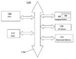
- FIG. 4illustrates a processor-based system 1100 including an imaging device 108 , CPU 1102 , RAM 1110 , I/O device 1106 , and removable memory 1115 .
- the imaging device 108contains a pixel array 140 operating under a rolling shutter constructed and operated as described herein.
- the processor-based system 1100is exemplary of a system having digital circuits that could include image sensor devices. Without being limiting, such a system could include a computer system, camera system, scanner, machine vision, vehicle navigation, video phone, surveillance system, auto focus system, star tracker system, motion detection system, image stabilization system, and other image sensing and/or processing system.
- the processor-based system 1100for example a camera system, generally comprises a central processing unit (CPU) 1102 , such as a microprocessor, that communicates with an input/output (I/O) device 1106 over a bus 1104 .
- Imaging device 308also communicates with the CPU 1102 over the bus 1104 .
- the processor-based system 1100also includes random access memory (RAM) 1110 , and can include removable memory 1115 , such as flash memory, which also communicates with CPU 1102 over the bus 1104 .
- Imaging device 308may be combined with a processor, such as a CPU, digital signal processor, or microprocessor, with or without memory storage on a single integrated circuit or on a different chip than the processor. Any of the memory storage devices in the processor-based system 1100 could store software for employing the above-described method.
- FIGS. 5 and 6alternate embodiments of the rolling shutter technique according to the present invention are shown. These alternate embodiments show other possible arrangements of hard reset rows, in which the reset rows are arranged non-consecutively.
- FIG. 5shows a rolling shutter technique comprising a read row 500 (at row 6 of the array 140 ) and three individual hard reset rows 501 - 503 arranged in alternate sequential rows (respective rows 15 , 17 and 19 ) down the array 140 .
- FIG. 5shows a rolling shutter technique comprising a read row 500 (at row 6 of the array 140 ) and three individual hard reset rows 501 - 503 arranged in alternate sequential rows (respective rows 15 , 17 and 19 ) down the array 140 .
- FIG. 6shows a rolling shutter technique comprising a read out row 600 (at row 6 of the array 140 ) and three pairs of hard reset rows 601 - 606 at respective rows 12 , 13 , 15 , 16 , 18 and 19 of the array 140 , each pair of reset rows being separated by a single row of pixels (respective rows 14 and 17 ) down the array 140 .
- read and hard reset rowscan be modified as circumstances dictate.
Landscapes
- Engineering & Computer Science (AREA)
- Multimedia (AREA)
- Signal Processing (AREA)
- Transforming Light Signals Into Electric Signals (AREA)
- Solid State Image Pick-Up Elements (AREA)
Abstract
Description
- The present invention relates to a rolling shutter for the prevention of blooming in a CMOS pixel cell array.
- Image sensors are used in a variety of digital image capture systems, including products such as scanners, copiers, and digital cameras. The image sensor is typically composed of an array of light-sensitive pixel cells that are electrically responsive to incident light reflected from an object or scene whose image is to be captured.
- A CMOS imager includes a focal plane array of pixel cells, each cell includes a photosensor, for example, a photogate, photoconductor or a photodiode overlying a substrate for producing a photo-generated charge in a doped region of the substrate. In a CMOS imager, the active elements of a pixel cell, for example a four transistor (4T) pixel cell, perform the necessary functions of (1) photon to charge conversion; (2) resetting a floating diffusion region to a known state; (3) transfer of charge to the floating diffusion region; (4) selection of a pixel cell for readout; and (5) output and amplification of a signal representing a reset voltage and a pixel signal voltage based on the photo-converted charges. The charge at the floating diffusion region is converted to a pixel or reset output voltage by a source follower output transistor.
- Exemplary CMOS imaging circuits, processing steps thereof, and detailed descriptions of the functions of various CMOS elements of an imaging circuit are described, for example, in U.S. Pat. Nos. 6,140,630, 6,376,868, 6,310,366, 6,326,652, 6,204,524, and 6,333,205, all assigned to Micron Technology, Inc. The disclosures of each of the forgoing patents are hereby incorporated by reference herein in their entirety.
- A conventional CMOS four-transistor (4T)
pixel cell 10 is illustrated inFIGS. 1A . The illustratedcell 10 includes apinned photodiode 13 as a photosensor. Alternatively, theCMOS cell 10 may include a photogate, photoconductor or other photon-to-charge converting device, in lieu of thepinned photodiode 13, as the initial accumulating area for photo-generated charge. Thephotodiode 13 includes a p+ surface accumulation layer and an underlying n- charge accumulation region formed in a p-type semiconductor substrate. In theexemplary pixel 10, accumulated charges are accumulated electrons. - The
pixel cell 10 has atransfer gate 7, which is part of a transfer transistor8, for transferring photocharges generated in the n- accumulation region to afloating diffusion region 3. Thefloating diffusion region 3 is further connected to agate 27 of asource follower transistor 28. Thesource follower transistor 28 provides an output signal to a row select transistor38 having agate 37 for selectively gating the output signal to a column line50. The column line50 is selected for readout by a columnselect transistor 52, which applies a current source54 to column line50. Areset transistor 18 having a gate17 resets thefloating diffusion region 3 to a specified charge level by connecting it to a supply voltage Vaa-pixbefore each charge transfer from the n- accumulation region of thephotodiode 13. FIG. 1B illustrates a block diagram of anexemplary CMOS imager 108 having apixel array 140 comprising a plurality of pixel cells arranged in a predetermined number of columns and rows, with each pixel cell being constructed as illustrated and described above with respect toFIGS. 1A or using other known pixel architectures. Attached to thearray 140 is signal processing circuitry for controlling thepixel array 140, as described herein, at least part of which may be formed in the substrate. The pixel cells of each row inarray 140 are all turned on at the same time by a row select line, and the pixel cells of each column are selectively output by respective column select lines. A plurality of TX, read, row select and column select lines are provided for theentire array 140. The row lines are selectively activated by arow driver 145 in response torow address decoder 155. The column select lines are selectively activated by acolumn driver 160 in response tocolumn address decoder 170. Thus, a row and column address is provided for each pixel cell.- The
CMOS imager 108 is operated by a timing andcontrol circuit 150, which controlsaddress decoders control circuit 150 also controls the row andcolumn driver circuitry column driver 160, on output lines, and are read by a sample and holdcircuit 161. Vrstis read from apixel cell 10 immediately after thefloating diffusion region 3 is reset. Vsigrepresents the amount of charges generated by the photosensitive element of thepixel cell 10 in response to applied light during an integration period. A differential signal (Vrst−Vsig) is produced bydifferential amplifier 162 for each readout pixel cell. The differential signal is digitized by an analog-to-digital converter175 (ADC). The analog todigital converter 175 supplies the digitized pixel signals to animage processor 180, which forms and outputs a digital image. - Blooming occurs when a photodiode or other photosensitive device is overexposed, i.e., the
photodiode 13 is exposed to more photons than it is capable of absorbing and converting to electrons. This is typically due to exposure of a pixel to an overly intense light source, or to exposing the pixel for too long a period of time. The excess electrons can spill over into pixels in nearby rows and columns. This overflow distorts the image, and can wash out portions of the image near the overexposed portion. - A typical technique for exposing and reading out images using
pixel array 140 is by using a rolling shutter. That is, as row N is being read out, row N+X is hard reset, with X representing a number of rows further down in thearray 140. A hard reset means that both the reset transistors and transfer transistors are turned on to reset the photodiode, and when the transfer transistor is turned off, an integration period begins. The time difference between a hard reset of a row and its subsequent readout is the pixel exposure time, also known as integration time. - Referring now to
FIGS. 2A-2F , the operation of a conventional rolling shutter on a portion of a conventionalCMOS pixel array 140 is now described. The rolling shutter, operated by control circuit150 (FIG. 1B ) includes aread row 200 and ahard reset row 201. An overexposed pixel210 and bloom region211 is also shown. For the purposes of this example, the integration period X of the rolling shutter is the time it takes to sequentially read out 10 rows. The integration period can be set responsive to the amount of incident light and on the capacity of thephotodiodes 13 in order to prevent individual pixels from overexposing and blooming during the integration period. - Referring now to
FIG. 2A , as read row200 (at row6) is being read out, hard reset row201 (at row16) is hard reset, which then begins an integration period for row16 where row16 begins to collect photons until the readrow 200 reaches row16.FIGS. 2B-2F show the row by row progression ofread row 200 andhard reset row 201, with thehard reset row 201 always10 rows ahead of theread row 200. Once rows6-15 are read out in sequence, row16 will then be read out, and so on. This conventional rolling shutter technique does not adequately compensate for blooming, however. - Blooming can often affect pixels several rows or columns away from the initially overexposed pixel. In many cases, the adjacent pixels, which absorb a large portion of the deflected electrons from the initial overexposed pixel, can be overexposed themselves and begin to deflect electrons. Additionally, many electrons may be deflected to pixels several rows or columns away.
- This blooming problem is exacerbated when, as is often the case in overexposure situations, large groups of adjacent pixels are exposed to intense light and become overexposed. The cumulative effect of the overexposed pixels can accelerate the displacement of extra electrons, overexposing and distorting pixels many rows and columns away from the initially overexposed pixels in a very short amount of time.
- Conventional rolling shutters cannot fully compensate for this phenomenon. Referring again to
FIGS. 2A-2F , an overexposed pixel210 having a bloom region211 is shown. For the purposes of this example, a single pixel210 is exposed to light of sufficient intensity to overload the photosensor charge accumulation region14 (seeFIG. 1A ) and send excess electrons as far away as five pixels in all directions. Thus, all pixels within the bloom region211, having a radius of approximately five pixels, will produce an inaccurate result because of the excess electrons from pixel210. - Referring again to
FIG. 2A , whenhard reset row 201 reaches and discharges row16, i.e., hard resets the pixels in the row), the effects of the overexposed pixel210 on the portion of the row in the bloom region211 are temporarily eliminated. However, as shown inFIG. 2B , the blooming effect on a portion of row16 can reemerge before the end of the integration period for row16. A modern pixel array can have in excess of 1000 rows; therefore, in this example where the integration time is 10 rows, an overexposed pixel210 can deflect electrons to nearby pixels for the time it takes to read out990 rows, or longer. Also, because electrons can be deflected farther than the dimensions of an individual pixel, the hard resetting of row17 will not prevent photon overflow to still integrating row16. Also, in situations where the light is particularly intense, or where the photon capacity of a pixel cell is particularly small, the portion of row17 in the bloom region211 may refill and overflow to row16 in less time than it takes to integrate one row, further distorting the portion of row16 in the bloom region211. FIGS. 2C-2F show the progression of the rolling shutter and its inability to fully compensate for blooming. Thehard reset row 201 must reach the overexposed pixel210 (at row21) to fully discharge the excess electrons by a hard reset, as shown inFIG. 2F . Before thehard reset row 201 reaches the overexposed pixel210 at row21, however, portions of rows16-20 in the bloom region211 will have already been distorted by the excess electrons which have been deflected from the pixel210 before hard reset, as shown inFIGS. 2B-2E . Although overexposed pixel210 is hard reset and stops contributing to the distortion of bloom region211, the effects of the excess electrons in bloom region211 will remain until the row is discharged, either by being hard reset for rows22+, or by being read out for rows16-20, distorting the portion of the image in that portion of the bloom region211.- There exists a need and desire for an improved rolling shutter to reduce blooming in CMOS pixel arrays caused by intense light sources and by pixel cells having small charge accumulation capacity.
- The present invention, as described in an exemplary embodiment, employs a rolling shutter technique having multiple hard reset rows that counteract the effects of blooming. The advantages are twofold. First, as the shutter progresses row-by-row down the array, each row is hard reset multiple times before the integration period begins, thereby ensuring that the row is in a true hard reset condition at the beginning of the integration period. Second, multiple leading rows are hard reset at the beginning of the integration period for a given row, thereby making it less likely that overexposed pixels several rows away will be able to distort the given row.
- According to the exemplary embodiment, as row N is read out, rows N+X, . . . N+X+(Y−1) are all hard reset, with X representing the integration time, expressed in rows, of the pixel and Y representing the number of hard reset rows in the shutter. Y can be as few as 2, and it is generally sufficient that Y be between 3 and 5.However, Y can be as large as the total number of rows in the array minus X (the number of rows needed to integrate the pixel result). According to other alternate embodiments, the hard reset rows may be arranged as non-consecutive rows.
- The foregoing and other advantages and features of the invention will become more apparent from the detailed description of exemplary embodiments provided below with reference to the accompanying drawings in which:
FIG. 1A is a schematic diagram of a conventional pixel cell;FIG. 1B depicts a block diagram of an imager device which can employ the invention;FIGS. 2A-2F show the operation of a conventional rolling shutter;FIGS. 3A-3D show the operation of a rolling shutter according to the present invention;FIG. 4 shows a processor system incorporating at least one imager device constructed in accordance with an embodiment of the invention; andFIG. 5 shows the arrangement of a rolling shutter according to an alternate embodiment of the present invention.FIG. 6 shows the arrangement of a rolling shutter according to another alternate embodiment of the present invention.- Referring now to
FIGS. 3A-3D , a portion of aCMOS pixel array 140 is shown. Thearray 140, overexposed pixel210 and bloom region211 have the same designations as discussed above with respect toFIGS. 2A-2F . A rolling shutter according to present invention, controlled by control circuit150 (FIG. 1B ) and having readrow 300 and hard reset rows301-305 (Y=5), is also shown. The integration time X of the rolling shutter is 10 rows, as inFIGS. 2A-2F . Thus, as eachrow 300 is sequentially read (designated as row N), rows301-305 will simultaneously be hard reset (designated as rows N+X through N+X+(Y−1)). - Thus, referring now to
FIG. 3A , as row5 is the readrow 300, rows15-19 are hard reset. By hard resetting multiple rows, a much more significant portion of the bloom region211 is hard reset before integration, thereby making it more difficult for the overexposed pixel to deflect or overflow electrons into rows that are still being integrated and being, or about to be read out. Here, row5 is being read out, while rows6-14 are still integrating. - Referring now to
FIG. 3B , as row6 becomes the readrow 300, rows16-20 are hard reset. Thus,row 20 is hard reset, while rows16-19 are hard reset again. - Referring now to
FIG. 3C , asrow 7 becomes the readrow 300, rows17-21 are hard reset. This is significant because the overexposed pixel210, located at row21, is now discharged. A portion of bloom region211 (rows22-26) remains distorted, but the row by row hard reset of these rows, beginning with row22 inFIG. 3D , will eliminate the distortion before the integration period begins for these respective rows. For pixel210 to become overexposed and bloom again, the pixel must be exposed to capacity in the time it takes the shutter to move down one row, when another hard reset will occur on row210. This is highly unlikely unless the light is abnormally intense, or unless the pixel210 has an extremely low photon capacity; in such a case, the integration period X could also be reduced to prevent blooming pixels during integration. - Referring now to
FIG. 3C , as row8 becomes the readrow 300, rows18-22, again including pixel210 in row21, are hard reset. Formerly overexposed pixel210 is hard reset five times in this example, thereby preventing reemergence of overexposure and blooming in the pixel210. - The number of hard reset rows Y in the above example is 5, but in practice, the number of hard reset rows Y may be anywhere between 2 and the total number of rows in the
pixel array 140, minus the number of rows X required for integration and read out of the pixels. This number of hard reset rows Y may be set based on the blooming that is expected based on other parameters of the imager and on the amount of incident light. As the reset rows301-305 reach the last row of thearray 140, the reset rows301-305 loop back to the first row of the array in sequence. - The invention is easily implemented in the
FIG. 1B imager device 18 by controlling the row reset and transfer signals applied to thearray 140 from therow decoder 155 androw driver 145 circuits under control ofcontrol circuit 150. FIG. 4 illustrates a processor-basedsystem 1100 including animaging device 108,CPU 1102,RAM 1110, I/O device 1106, andremovable memory 1115. Theimaging device 108 contains apixel array 140 operating under a rolling shutter constructed and operated as described herein. The processor-basedsystem 1100 is exemplary of a system having digital circuits that could include image sensor devices. Without being limiting, such a system could include a computer system, camera system, scanner, machine vision, vehicle navigation, video phone, surveillance system, auto focus system, star tracker system, motion detection system, image stabilization system, and other image sensing and/or processing system.- The processor-based
system 1100, for example a camera system, generally comprises a central processing unit (CPU)1102, such as a microprocessor, that communicates with an input/output (I/O)device 1106 over abus 1104.Imaging device 308 also communicates with theCPU 1102 over thebus 1104. The processor-basedsystem 1100 also includes random access memory (RAM)1110, and can includeremovable memory 1115, such as flash memory, which also communicates withCPU 1102 over thebus 1104.Imaging device 308 may be combined with a processor, such as a CPU, digital signal processor, or microprocessor, with or without memory storage on a single integrated circuit or on a different chip than the processor. Any of the memory storage devices in the processor-basedsystem 1100 could store software for employing the above-described method. - Referring now to
FIGS. 5 and 6 , alternate embodiments of the rolling shutter technique according to the present invention are shown. These alternate embodiments show other possible arrangements of hard reset rows, in which the reset rows are arranged non-consecutively.FIG. 5 shows a rolling shutter technique comprising a read row500 (at row6 of the array140) and three individual hard reset rows501-503 arranged in alternate sequential rows (respective rows15,17 and19) down thearray 140.FIG. 6 shows a rolling shutter technique comprising a read out row600 (at row6 of the array140) and three pairs of hard reset rows601-606 atrespective rows array 140, each pair of reset rows being separated by a single row of pixels (respective rows14 and17) down thearray 140. These and other arrangements of read and hard reset rows can be modified as circumstances dictate. - The above description and drawings are only to be considered illustrative of exemplary embodiments which achieve the features and advantages of the invention. Modification of, and substitutions to, specific process conditions and structures can be made without departing from the spirit and scope of the invention. Accordingly, the invention is not to be considered as being limited by the foregoing description and drawings, but is only limited by the scope of the appended claims.
Claims (24)
Priority Applications (2)
| Application Number | Priority Date | Filing Date | Title |
|---|---|---|---|
| US11/114,094US7619670B2 (en) | 2005-04-26 | 2005-04-26 | Rolling shutter for prevention of blooming |
| US12/603,759US8026967B2 (en) | 2005-04-26 | 2009-10-22 | Rolling shutter for prevention of blooming |
Applications Claiming Priority (1)
| Application Number | Priority Date | Filing Date | Title |
|---|---|---|---|
| US11/114,094US7619670B2 (en) | 2005-04-26 | 2005-04-26 | Rolling shutter for prevention of blooming |
Related Child Applications (1)
| Application Number | Title | Priority Date | Filing Date |
|---|---|---|---|
| US12/603,759ContinuationUS8026967B2 (en) | 2005-04-26 | 2009-10-22 | Rolling shutter for prevention of blooming |
Publications (2)
| Publication Number | Publication Date |
|---|---|
| US20060238632A1true US20060238632A1 (en) | 2006-10-26 |
| US7619670B2 US7619670B2 (en) | 2009-11-17 |
Family
ID=37186436
Family Applications (2)
| Application Number | Title | Priority Date | Filing Date |
|---|---|---|---|
| US11/114,094Active2027-07-29US7619670B2 (en) | 2005-04-26 | 2005-04-26 | Rolling shutter for prevention of blooming |
| US12/603,759Expired - LifetimeUS8026967B2 (en) | 2005-04-26 | 2009-10-22 | Rolling shutter for prevention of blooming |
Family Applications After (1)
| Application Number | Title | Priority Date | Filing Date |
|---|---|---|---|
| US12/603,759Expired - LifetimeUS8026967B2 (en) | 2005-04-26 | 2009-10-22 | Rolling shutter for prevention of blooming |
Country Status (1)
| Country | Link |
|---|---|
| US (2) | US7619670B2 (en) |
Cited By (26)
| Publication number | Priority date | Publication date | Assignee | Title |
|---|---|---|---|---|
| US20060109373A1 (en)* | 2004-11-22 | 2006-05-25 | Seiko Epson Corporation | Imaging device and imaging apparatus |
| US20080158402A1 (en)* | 2006-12-27 | 2008-07-03 | Sony Corporation | Solid-state imaging device |
| US20080309806A1 (en)* | 2007-06-18 | 2008-12-18 | Canon Kabushiki Kaisha | Imaging system, image sensor, and method of controlling imaging system |
| US20080309810A1 (en)* | 2007-06-15 | 2008-12-18 | Scott Smith | Images with high speed digital frame transfer and frame processing |
| US20090122168A1 (en)* | 2007-11-14 | 2009-05-14 | Novatek Microelectronics Corp. | Method for resetting image sensing and image sensing device using the same |
| US20090153710A1 (en)* | 2007-12-13 | 2009-06-18 | Motorola, Inc. | Digital imager with dual rolling shutters |
| US8093541B2 (en) | 2008-06-05 | 2012-01-10 | Aptina Imaging Corporation | Anti-blooming protection of pixels in a pixel array for multiple scaling modes |
| US20120314111A1 (en)* | 2010-02-26 | 2012-12-13 | Panasonic Corporation | Imaging device and solid-state imaging device |
| WO2014013340A3 (en)* | 2012-07-16 | 2014-03-13 | Varian Medical Systems International Ag | Circuitry and method for collecting image array data with separate addressing and dynamic clamping of pixels to allow for faster pixel data readout and full removal of pixel charges |
| US20140232867A1 (en)* | 2013-02-18 | 2014-08-21 | Tsinghua University | Method for determining attitude of star sensor based on rolling shutter imaging |
| US9319605B2 (en) | 2013-03-15 | 2016-04-19 | Rambus Inc. | Increasing dynamic range using multisampling |
| US9496308B2 (en) | 2011-06-09 | 2016-11-15 | Sionyx, Llc | Process module for increasing the response of backside illuminated photosensitive imagers and associated methods |
| US20170070677A1 (en)* | 2015-09-07 | 2017-03-09 | Axis Ab | Method and device for setting a focus of a camera |
| US9673243B2 (en) | 2009-09-17 | 2017-06-06 | Sionyx, Llc | Photosensitive imaging devices and associated methods |
| US9673250B2 (en) | 2013-06-29 | 2017-06-06 | Sionyx, Llc | Shallow trench textured regions and associated methods |
| US9741761B2 (en) | 2010-04-21 | 2017-08-22 | Sionyx, Llc | Photosensitive imaging devices and associated methods |
| US9762830B2 (en) | 2013-02-15 | 2017-09-12 | Sionyx, Llc | High dynamic range CMOS image sensor having anti-blooming properties and associated methods |
| US9761739B2 (en) | 2010-06-18 | 2017-09-12 | Sionyx, Llc | High speed photosensitive devices and associated methods |
| WO2017185783A1 (en)* | 2016-04-28 | 2017-11-02 | 努比亚技术有限公司 | Mobile terminal, exposure method therefor, and computer storage medium |
| US9905599B2 (en) | 2012-03-22 | 2018-02-27 | Sionyx, Llc | Pixel isolation elements, devices and associated methods |
| US9911781B2 (en) | 2009-09-17 | 2018-03-06 | Sionyx, Llc | Photosensitive imaging devices and associated methods |
| US9939251B2 (en) | 2013-03-15 | 2018-04-10 | Sionyx, Llc | Three dimensional imaging utilizing stacked imager devices and associated methods |
| US10244188B2 (en) | 2011-07-13 | 2019-03-26 | Sionyx, Llc | Biometric imaging devices and associated methods |
| US10374109B2 (en) | 2001-05-25 | 2019-08-06 | President And Fellows Of Harvard College | Silicon-based visible and near-infrared optoelectric devices |
| US10741399B2 (en) | 2004-09-24 | 2020-08-11 | President And Fellows Of Harvard College | Femtosecond laser-induced formation of submicrometer spikes on a semiconductor substrate |
| DE102020122748B3 (en) | 2020-08-31 | 2022-02-10 | Jena-Optronik Gesellschaft mit beschränkter Haftung | Method, device and computer program product for determining the attitude of a spacecraft in space |
Families Citing this family (8)
| Publication number | Priority date | Publication date | Assignee | Title |
|---|---|---|---|---|
| JP5163935B2 (en)* | 2007-05-17 | 2013-03-13 | ソニー株式会社 | Image sensor |
| TWI433307B (en)* | 2008-10-22 | 2014-04-01 | Sony Corp | Solid-state image sensor, driving method thereof, imaging device and electronic device |
| US8903043B2 (en) | 2011-10-24 | 2014-12-02 | Bruker Axs, Inc. | Method for correcting timing skew in X-ray data read out of an X-ray detector in a rolling shutter mode |
| JP2013123107A (en)* | 2011-12-09 | 2013-06-20 | Sony Corp | Solid-state image pickup device, solid-state image pickup device driving method, and electronic apparatus |
| US9667865B2 (en) | 2012-11-03 | 2017-05-30 | Apple Inc. | Optical demodulation using an image sensor |
| US9100600B2 (en) | 2013-07-10 | 2015-08-04 | Samsung Electronics Co., Ltd. | Anti-blooming shutter control in image sensors |
| CN111412915B (en)* | 2020-04-21 | 2022-08-26 | 中国科学院光电技术研究所 | Rolling shutter exposure star sensor star point position correction method based on average speed |
| US11330221B1 (en) | 2020-10-28 | 2022-05-10 | Gigajot Technology, Inc. | Dual-progression pixel readout |
Citations (3)
| Publication number | Priority date | Publication date | Assignee | Title |
|---|---|---|---|---|
| US5812528A (en)* | 1995-11-17 | 1998-09-22 | Telecommunications Techniques Corporation | Measuring round trip time in ATM network virtual connections |
| US20020175269A1 (en)* | 2001-04-04 | 2002-11-28 | Krymski Alexander I. | Method and apparatus for reducing kTC noise in an active pixel sensor (APS) device |
| US6809766B1 (en)* | 1998-03-11 | 2004-10-26 | Micro Technology, Inc. | Look ahead rolling shutter system in CMOS sensors |
- 2005
- 2005-04-26USUS11/114,094patent/US7619670B2/enactiveActive
- 2009
- 2009-10-22USUS12/603,759patent/US8026967B2/ennot_activeExpired - Lifetime
Patent Citations (3)
| Publication number | Priority date | Publication date | Assignee | Title |
|---|---|---|---|---|
| US5812528A (en)* | 1995-11-17 | 1998-09-22 | Telecommunications Techniques Corporation | Measuring round trip time in ATM network virtual connections |
| US6809766B1 (en)* | 1998-03-11 | 2004-10-26 | Micro Technology, Inc. | Look ahead rolling shutter system in CMOS sensors |
| US20020175269A1 (en)* | 2001-04-04 | 2002-11-28 | Krymski Alexander I. | Method and apparatus for reducing kTC noise in an active pixel sensor (APS) device |
Cited By (48)
| Publication number | Priority date | Publication date | Assignee | Title |
|---|---|---|---|---|
| US10374109B2 (en) | 2001-05-25 | 2019-08-06 | President And Fellows Of Harvard College | Silicon-based visible and near-infrared optoelectric devices |
| US10741399B2 (en) | 2004-09-24 | 2020-08-11 | President And Fellows Of Harvard College | Femtosecond laser-induced formation of submicrometer spikes on a semiconductor substrate |
| US20060109373A1 (en)* | 2004-11-22 | 2006-05-25 | Seiko Epson Corporation | Imaging device and imaging apparatus |
| US7511752B2 (en)* | 2004-11-22 | 2009-03-31 | Seiko Epson Corporation | Imaging device and imaging apparatus with reset unit that resets plural lines simultaneously |
| US20080158402A1 (en)* | 2006-12-27 | 2008-07-03 | Sony Corporation | Solid-state imaging device |
| US7932945B2 (en)* | 2006-12-27 | 2011-04-26 | Sony Corporation | Solid-state imaging device |
| US20080309810A1 (en)* | 2007-06-15 | 2008-12-18 | Scott Smith | Images with high speed digital frame transfer and frame processing |
| US7884871B2 (en) | 2007-06-15 | 2011-02-08 | Aptina Imaging Corporation | Images with high speed digital frame transfer and frame processing |
| US20090268083A1 (en)* | 2007-06-18 | 2009-10-29 | Canon Kabushiki Kaisha | Imaging system, image sensor, and method of controlling imaging system |
| US7630009B2 (en)* | 2007-06-18 | 2009-12-08 | Canon Kabushiki Kaisha | Imaging system, image sensor, and method of controlling imaging system |
| US20080309806A1 (en)* | 2007-06-18 | 2008-12-18 | Canon Kabushiki Kaisha | Imaging system, image sensor, and method of controlling imaging system |
| US8159578B2 (en) | 2007-06-18 | 2012-04-17 | Canon Kabushiki Kaisha | Imaging system, image sensor, and method of controlling imaging system |
| US20090122168A1 (en)* | 2007-11-14 | 2009-05-14 | Novatek Microelectronics Corp. | Method for resetting image sensing and image sensing device using the same |
| US7948537B2 (en)* | 2007-11-14 | 2011-05-24 | Novatek Microelectronics Corp. | Method for resetting image sensing and image sensing device using the same |
| US8223235B2 (en) | 2007-12-13 | 2012-07-17 | Motorola Mobility, Inc. | Digital imager with dual rolling shutters |
| US20090153710A1 (en)* | 2007-12-13 | 2009-06-18 | Motorola, Inc. | Digital imager with dual rolling shutters |
| US8093541B2 (en) | 2008-06-05 | 2012-01-10 | Aptina Imaging Corporation | Anti-blooming protection of pixels in a pixel array for multiple scaling modes |
| US9911781B2 (en) | 2009-09-17 | 2018-03-06 | Sionyx, Llc | Photosensitive imaging devices and associated methods |
| US10361232B2 (en) | 2009-09-17 | 2019-07-23 | Sionyx, Llc | Photosensitive imaging devices and associated methods |
| US9673243B2 (en) | 2009-09-17 | 2017-06-06 | Sionyx, Llc | Photosensitive imaging devices and associated methods |
| US8743273B2 (en)* | 2010-02-26 | 2014-06-03 | Panasonic Corporation | Imaging device and solid-state imaging device |
| US20120314111A1 (en)* | 2010-02-26 | 2012-12-13 | Panasonic Corporation | Imaging device and solid-state imaging device |
| US10229951B2 (en) | 2010-04-21 | 2019-03-12 | Sionyx, Llc | Photosensitive imaging devices and associated methods |
| US9741761B2 (en) | 2010-04-21 | 2017-08-22 | Sionyx, Llc | Photosensitive imaging devices and associated methods |
| US10505054B2 (en) | 2010-06-18 | 2019-12-10 | Sionyx, Llc | High speed photosensitive devices and associated methods |
| US9761739B2 (en) | 2010-06-18 | 2017-09-12 | Sionyx, Llc | High speed photosensitive devices and associated methods |
| US9666636B2 (en) | 2011-06-09 | 2017-05-30 | Sionyx, Llc | Process module for increasing the response of backside illuminated photosensitive imagers and associated methods |
| US9496308B2 (en) | 2011-06-09 | 2016-11-15 | Sionyx, Llc | Process module for increasing the response of backside illuminated photosensitive imagers and associated methods |
| US10269861B2 (en) | 2011-06-09 | 2019-04-23 | Sionyx, Llc | Process module for increasing the response of backside illuminated photosensitive imagers and associated methods |
| US10244188B2 (en) | 2011-07-13 | 2019-03-26 | Sionyx, Llc | Biometric imaging devices and associated methods |
| US10224359B2 (en) | 2012-03-22 | 2019-03-05 | Sionyx, Llc | Pixel isolation elements, devices and associated methods |
| US9905599B2 (en) | 2012-03-22 | 2018-02-27 | Sionyx, Llc | Pixel isolation elements, devices and associated methods |
| WO2014013340A3 (en)* | 2012-07-16 | 2014-03-13 | Varian Medical Systems International Ag | Circuitry and method for collecting image array data with separate addressing and dynamic clamping of pixels to allow for faster pixel data readout and full removal of pixel charges |
| US8803061B2 (en) | 2012-07-16 | 2014-08-12 | Varian Medical Systems International Ag | Circuitry and method for collecting image array data with separate addressing and dynamic clamping of pixels to allow for faster pixel data readout and full removal of pixel charges |
| CN104604216A (en)* | 2012-07-16 | 2015-05-06 | 瓦里安医疗系统国际股份公司 | Circuits and methods for acquiring image array data with independent pixel addressing and dynamic clamping allowing for faster pixel data readout and complete pixel charge removal |
| US9762830B2 (en) | 2013-02-15 | 2017-09-12 | Sionyx, Llc | High dynamic range CMOS image sensor having anti-blooming properties and associated methods |
| US9503653B2 (en)* | 2013-02-18 | 2016-11-22 | Tsinghua University | Method for determining attitude of star sensor based on rolling shutter imaging |
| US20140232867A1 (en)* | 2013-02-18 | 2014-08-21 | Tsinghua University | Method for determining attitude of star sensor based on rolling shutter imaging |
| US9939251B2 (en) | 2013-03-15 | 2018-04-10 | Sionyx, Llc | Three dimensional imaging utilizing stacked imager devices and associated methods |
| US9319605B2 (en) | 2013-03-15 | 2016-04-19 | Rambus Inc. | Increasing dynamic range using multisampling |
| US10347682B2 (en) | 2013-06-29 | 2019-07-09 | Sionyx, Llc | Shallow trench textured regions and associated methods |
| US9673250B2 (en) | 2013-06-29 | 2017-06-06 | Sionyx, Llc | Shallow trench textured regions and associated methods |
| US11069737B2 (en) | 2013-06-29 | 2021-07-20 | Sionyx, Llc | Shallow trench textured regions and associated methods |
| US20170070677A1 (en)* | 2015-09-07 | 2017-03-09 | Axis Ab | Method and device for setting a focus of a camera |
| US9906724B2 (en)* | 2015-09-07 | 2018-02-27 | Axis Ab | Method and device for setting a focus of a camera |
| WO2017185783A1 (en)* | 2016-04-28 | 2017-11-02 | 努比亚技术有限公司 | Mobile terminal, exposure method therefor, and computer storage medium |
| DE102020122748B3 (en) | 2020-08-31 | 2022-02-10 | Jena-Optronik Gesellschaft mit beschränkter Haftung | Method, device and computer program product for determining the attitude of a spacecraft in space |
| WO2022043247A1 (en) | 2020-08-31 | 2022-03-03 | Jena-Optronik Gmbh | Method, device and computer program product for determining the position of a spacecraft in space |
Also Published As
| Publication number | Publication date |
|---|---|
| US8026967B2 (en) | 2011-09-27 |
| US7619670B2 (en) | 2009-11-17 |
| US20100039542A1 (en) | 2010-02-18 |
Similar Documents
| Publication | Publication Date | Title |
|---|---|---|
| US8026967B2 (en) | Rolling shutter for prevention of blooming | |
| US12250470B2 (en) | Method and apparatus providing pixel array having automatic light control pixels and image capture pixels | |
| JP7246009B2 (en) | Imaging device | |
| CN209488695U (en) | Image Sensor Pixels | |
| KR200492043Y1 (en) | Global shutter image sensor pixels having improved shutter efficiency | |
| US8502898B2 (en) | Method, apparatus, and system providing a rectilinear pixel grid with radially scaled pixels | |
| US7427736B2 (en) | Method and apparatus for providing a rolling double reset timing for global storage in image sensors | |
| CN110248126B (en) | Dual conversion gain circuit with buried channel | |
| US20080210986A1 (en) | Global shutter pixel with charge storage region | |
| US20070035649A1 (en) | Image pixel reset through dual conversion gain gate | |
| US10917588B2 (en) | Imaging sensors with per-pixel control | |
| US8072520B2 (en) | Dual pinned diode pixel with shutter | |
| US8077236B2 (en) | Method and apparatus providing reduced metal routing in imagers | |
| US7619671B2 (en) | Method, apparatus and system for charge injection suppression in active pixel sensors | |
| CN110557583B (en) | Image sensor, method of operating image sensor, and imaging system | |
| US7787032B2 (en) | Method and apparatus for dark current reduction in image sensors | |
| US20060268140A1 (en) | Method and apparatus for reducing noise in analog amplifier circuits and solid state imagers employing such circuits | |
| WO2024031300A1 (en) | Photon counting pixel and method of operation thereof | |
| JP2011040482A (en) | Solid-state imaging apparatus |
Legal Events
| Date | Code | Title | Description |
|---|---|---|---|
| AS | Assignment | Owner name:MICRON TECHNOLOGY, INC., IDAHO Free format text:ASSIGNMENT OF ASSIGNORS INTEREST;ASSIGNOR:SHAH, JOEY;REEL/FRAME:016508/0273 Effective date:20050418 | |
| FEPP | Fee payment procedure | Free format text:PAYOR NUMBER ASSIGNED (ORIGINAL EVENT CODE: ASPN); ENTITY STATUS OF PATENT OWNER: LARGE ENTITY | |
| STCF | Information on status: patent grant | Free format text:PATENTED CASE | |
| CC | Certificate of correction | ||
| CC | Certificate of correction | ||
| FPAY | Fee payment | Year of fee payment:4 | |
| AS | Assignment | Owner name:U.S. BANK NATIONAL ASSOCIATION, AS COLLATERAL AGENT, CALIFORNIA Free format text:SECURITY INTEREST;ASSIGNOR:MICRON TECHNOLOGY, INC.;REEL/FRAME:038669/0001 Effective date:20160426 Owner name:U.S. BANK NATIONAL ASSOCIATION, AS COLLATERAL AGEN Free format text:SECURITY INTEREST;ASSIGNOR:MICRON TECHNOLOGY, INC.;REEL/FRAME:038669/0001 Effective date:20160426 | |
| AS | Assignment | Owner name:MORGAN STANLEY SENIOR FUNDING, INC., AS COLLATERAL AGENT, MARYLAND Free format text:PATENT SECURITY AGREEMENT;ASSIGNOR:MICRON TECHNOLOGY, INC.;REEL/FRAME:038954/0001 Effective date:20160426 Owner name:MORGAN STANLEY SENIOR FUNDING, INC., AS COLLATERAL Free format text:PATENT SECURITY AGREEMENT;ASSIGNOR:MICRON TECHNOLOGY, INC.;REEL/FRAME:038954/0001 Effective date:20160426 | |
| FPAY | Fee payment | Year of fee payment:8 | |
| AS | Assignment | Owner name:U.S. BANK NATIONAL ASSOCIATION, AS COLLATERAL AGENT, CALIFORNIA Free format text:CORRECTIVE ASSIGNMENT TO CORRECT THE REPLACE ERRONEOUSLY FILED PATENT #7358718 WITH THE CORRECT PATENT #7358178 PREVIOUSLY RECORDED ON REEL 038669 FRAME 0001. ASSIGNOR(S) HEREBY CONFIRMS THE SECURITY INTEREST;ASSIGNOR:MICRON TECHNOLOGY, INC.;REEL/FRAME:043079/0001 Effective date:20160426 Owner name:U.S. BANK NATIONAL ASSOCIATION, AS COLLATERAL AGEN Free format text:CORRECTIVE ASSIGNMENT TO CORRECT THE REPLACE ERRONEOUSLY FILED PATENT #7358718 WITH THE CORRECT PATENT #7358178 PREVIOUSLY RECORDED ON REEL 038669 FRAME 0001. ASSIGNOR(S) HEREBY CONFIRMS THE SECURITY INTEREST;ASSIGNOR:MICRON TECHNOLOGY, INC.;REEL/FRAME:043079/0001 Effective date:20160426 | |
| AS | Assignment | Owner name:JPMORGAN CHASE BANK, N.A., AS COLLATERAL AGENT, ILLINOIS Free format text:SECURITY INTEREST;ASSIGNORS:MICRON TECHNOLOGY, INC.;MICRON SEMICONDUCTOR PRODUCTS, INC.;REEL/FRAME:047540/0001 Effective date:20180703 Owner name:JPMORGAN CHASE BANK, N.A., AS COLLATERAL AGENT, IL Free format text:SECURITY INTEREST;ASSIGNORS:MICRON TECHNOLOGY, INC.;MICRON SEMICONDUCTOR PRODUCTS, INC.;REEL/FRAME:047540/0001 Effective date:20180703 | |
| AS | Assignment | Owner name:MICRON TECHNOLOGY, INC., IDAHO Free format text:RELEASE BY SECURED PARTY;ASSIGNOR:U.S. BANK NATIONAL ASSOCIATION, AS COLLATERAL AGENT;REEL/FRAME:047243/0001 Effective date:20180629 | |
| AS | Assignment | Owner name:MICRON TECHNOLOGY, INC., IDAHO Free format text:RELEASE BY SECURED PARTY;ASSIGNOR:MORGAN STANLEY SENIOR FUNDING, INC., AS COLLATERAL AGENT;REEL/FRAME:050937/0001 Effective date:20190731 | |
| AS | Assignment | Owner name:MICRON SEMICONDUCTOR PRODUCTS, INC., IDAHO Free format text:RELEASE BY SECURED PARTY;ASSIGNOR:JPMORGAN CHASE BANK, N.A., AS COLLATERAL AGENT;REEL/FRAME:051028/0001 Effective date:20190731 Owner name:MICRON TECHNOLOGY, INC., IDAHO Free format text:RELEASE BY SECURED PARTY;ASSIGNOR:JPMORGAN CHASE BANK, N.A., AS COLLATERAL AGENT;REEL/FRAME:051028/0001 Effective date:20190731 | |
| MAFP | Maintenance fee payment | Free format text:PAYMENT OF MAINTENANCE FEE, 12TH YEAR, LARGE ENTITY (ORIGINAL EVENT CODE: M1553); ENTITY STATUS OF PATENT OWNER: LARGE ENTITY Year of fee payment:12 |