US20060237791A1 - Ultra thin body fully-depleted SOI MOSFETs - Google Patents
Ultra thin body fully-depleted SOI MOSFETsDownload PDFInfo
- Publication number
- US20060237791A1 US20060237791A1US11/473,757US47375706AUS2006237791A1US 20060237791 A1US20060237791 A1US 20060237791A1US 47375706 AUS47375706 AUS 47375706AUS 2006237791 A1US2006237791 A1US 2006237791A1
- Authority
- US
- United States
- Prior art keywords
- soi
- gate
- thickness
- channel
- mosfet
- Prior art date
- Legal status (The legal status is an assumption and is not a legal conclusion. Google has not performed a legal analysis and makes no representation as to the accuracy of the status listed.)
- Granted
Links
- 239000000758substrateSubstances0.000claimsdescription35
- 125000006850spacer groupChemical group0.000claimsdescription18
- 239000004020conductorSubstances0.000claimsdescription16
- 239000004065semiconductorSubstances0.000claimsdescription16
- 229910021420polycrystalline siliconInorganic materials0.000claimsdescription15
- 229920005591polysiliconPolymers0.000claimsdescription15
- 239000012212insulatorSubstances0.000claimsdescription6
- 238000009792diffusion processMethods0.000claimsdescription5
- 229910044991metal oxideInorganic materials0.000claimsdescription4
- 150000004706metal oxidesChemical class0.000claimsdescription4
- 230000005669field effectEffects0.000claimsdescription3
- 230000007423decreaseEffects0.000claims2
- 238000000034methodMethods0.000abstractdescription43
- IJGRMHOSHXDMSA-UHFFFAOYSA-NAtomic nitrogenChemical compoundN#NIJGRMHOSHXDMSA-UHFFFAOYSA-N0.000abstractdescription16
- 230000015572biosynthetic processEffects0.000abstractdescription10
- 230000003647oxidationEffects0.000abstractdescription10
- 238000007254oxidation reactionMethods0.000abstractdescription10
- 229910052757nitrogenInorganic materials0.000abstractdescription9
- 238000012545processingMethods0.000abstractdescription7
- 239000000126substanceSubstances0.000abstractdescription4
- 230000003247decreasing effectEffects0.000abstractdescription2
- 239000000463materialSubstances0.000description16
- 238000005530etchingMethods0.000description14
- 150000002500ionsChemical class0.000description13
- XUIMIQQOPSSXEZ-UHFFFAOYSA-NSiliconChemical compound[Si]XUIMIQQOPSSXEZ-UHFFFAOYSA-N0.000description10
- 229910052710siliconInorganic materials0.000description10
- 239000010703siliconSubstances0.000description10
- 239000007943implantSubstances0.000description9
- 229910052731fluorineInorganic materials0.000description7
- 239000011737fluorineSubstances0.000description7
- VYPSYNLAJGMNEJ-UHFFFAOYSA-NSilicium dioxideChemical compoundO=[Si]=OVYPSYNLAJGMNEJ-UHFFFAOYSA-N0.000description6
- 238000005137deposition processMethods0.000description6
- YCKRFDGAMUMZLT-UHFFFAOYSA-NFluorine atomChemical compound[F]YCKRFDGAMUMZLT-UHFFFAOYSA-N0.000description5
- 238000000137annealingMethods0.000description5
- 238000000151depositionMethods0.000description5
- 230000008021depositionEffects0.000description5
- 239000003989dielectric materialSubstances0.000description5
- 239000002019doping agentSubstances0.000description5
- 238000005516engineering processMethods0.000description5
- -1fluorine ionsChemical class0.000description5
- 238000002513implantationMethods0.000description5
- BOTDANWDWHJENH-UHFFFAOYSA-NTetraethyl orthosilicateChemical compoundCCO[Si](OCC)(OCC)OCCBOTDANWDWHJENH-UHFFFAOYSA-N0.000description4
- 238000005229chemical vapour depositionMethods0.000description4
- 238000005468ion implantationMethods0.000description4
- 229910052751metalInorganic materials0.000description4
- 239000002184metalSubstances0.000description4
- 229920002120photoresistant polymerPolymers0.000description4
- 229910021332silicideInorganic materials0.000description4
- 229910052581Si3N4Inorganic materials0.000description3
- 125000004429atomChemical group0.000description3
- 229910052681coesiteInorganic materials0.000description3
- 229910052906cristobaliteInorganic materials0.000description3
- 125000005843halogen groupChemical group0.000description3
- 238000002955isolationMethods0.000description3
- 238000001459lithographyMethods0.000description3
- 150000004767nitridesChemical class0.000description3
- 238000000623plasma-assisted chemical vapour depositionMethods0.000description3
- 239000000377silicon dioxideSubstances0.000description3
- 229910052682stishoviteInorganic materials0.000description3
- 238000012546transferMethods0.000description3
- 229910052905tridymiteInorganic materials0.000description3
- GWEVSGVZZGPLCZ-UHFFFAOYSA-NTitan oxideChemical compoundO=[Ti]=OGWEVSGVZZGPLCZ-UHFFFAOYSA-N0.000description2
- MCMNRKCIXSYSNV-UHFFFAOYSA-NZirconium dioxideChemical compoundO=[Zr]=OMCMNRKCIXSYSNV-UHFFFAOYSA-N0.000description2
- QVGXLLKOCUKJST-UHFFFAOYSA-Natomic oxygenChemical compound[O]QVGXLLKOCUKJST-UHFFFAOYSA-N0.000description2
- 210000000746body regionAnatomy0.000description2
- 230000001419dependent effectEffects0.000description2
- 230000000694effectsEffects0.000description2
- 238000001704evaporationMethods0.000description2
- 230000008020evaporationEffects0.000description2
- 238000010438heat treatmentMethods0.000description2
- 239000011810insulating materialSubstances0.000description2
- 238000004519manufacturing processMethods0.000description2
- 150000002739metalsChemical class0.000description2
- 229910052760oxygenInorganic materials0.000description2
- 239000001301oxygenSubstances0.000description2
- 238000001020plasma etchingMethods0.000description2
- FVBUAEGBCNSCDD-UHFFFAOYSA-Nsilicide(4-)Chemical group[Si-4]FVBUAEGBCNSCDD-UHFFFAOYSA-N0.000description2
- 229910052814silicon oxideInorganic materials0.000description2
- 229910052721tungstenInorganic materials0.000description2
- ZOXJGFHDIHLPTG-UHFFFAOYSA-NBoronChemical compound[B]ZOXJGFHDIHLPTG-UHFFFAOYSA-N0.000description1
- OAICVXFJPJFONN-UHFFFAOYSA-NPhosphorusChemical compound[P]OAICVXFJPJFONN-UHFFFAOYSA-N0.000description1
- 229910003811SiGeCInorganic materials0.000description1
- 229910000577Silicon-germaniumInorganic materials0.000description1
- YPDSOAPSWYHANB-UHFFFAOYSA-N[N].[F]Chemical compound[N].[F]YPDSOAPSWYHANB-UHFFFAOYSA-N0.000description1
- 229910052782aluminiumInorganic materials0.000description1
- PNEYBMLMFCGWSK-UHFFFAOYSA-Naluminium oxideInorganic materials[O-2].[O-2].[O-2].[Al+3].[Al+3]PNEYBMLMFCGWSK-UHFFFAOYSA-N0.000description1
- 229910021417amorphous siliconInorganic materials0.000description1
- 229910001423beryllium ionInorganic materials0.000description1
- 229910052796boronInorganic materials0.000description1
- 238000000224chemical solution depositionMethods0.000description1
- 230000000295complement effectEffects0.000description1
- 229910052802copperInorganic materials0.000description1
- 229910052593corundumInorganic materials0.000description1
- 238000000280densificationMethods0.000description1
- 238000011982device technologyMethods0.000description1
- 238000001312dry etchingMethods0.000description1
- 238000011049fillingMethods0.000description1
- 238000005429filling processMethods0.000description1
- CJNBYAVZURUTKZ-UHFFFAOYSA-Nhafnium(IV) oxideInorganic materialsO=[Hf]=OCJNBYAVZURUTKZ-UHFFFAOYSA-N0.000description1
- 238000011065in-situ storageMethods0.000description1
- 238000010884ion-beam techniqueMethods0.000description1
- 229910052741iridiumInorganic materials0.000description1
- MRELNEQAGSRDBK-UHFFFAOYSA-Nlanthanum oxideInorganic materials[O-2].[O-2].[O-2].[La+3].[La+3]MRELNEQAGSRDBK-UHFFFAOYSA-N0.000description1
- 238000000608laser ablationMethods0.000description1
- 239000000203mixtureSubstances0.000description1
- 229910003465moissaniteInorganic materials0.000description1
- 229910052750molybdenumInorganic materials0.000description1
- 229910052759nickelInorganic materials0.000description1
- 150000002829nitrogenChemical class0.000description1
- KTUFCUMIWABKDW-UHFFFAOYSA-Noxo(oxolanthaniooxy)lanthanumChemical compoundO=[La]O[La]=OKTUFCUMIWABKDW-UHFFFAOYSA-N0.000description1
- 238000012856packingMethods0.000description1
- 229910052763palladiumInorganic materials0.000description1
- 229910052698phosphorusInorganic materials0.000description1
- 239000011574phosphorusSubstances0.000description1
- 238000007747platingMethods0.000description1
- 229910052697platinumInorganic materials0.000description1
- 230000005855radiationEffects0.000description1
- 239000003870refractory metalSubstances0.000description1
- 229910052702rheniumInorganic materials0.000description1
- 229910052707rutheniumInorganic materials0.000description1
- 238000000926separation methodMethods0.000description1
- 239000005368silicate glassSubstances0.000description1
- 229910010271silicon carbideInorganic materials0.000description1
- 238000004088simulationMethods0.000description1
- 238000004544sputter depositionMethods0.000description1
- 229910052715tantalumInorganic materials0.000description1
- PBCFLUZVCVVTBY-UHFFFAOYSA-Ntantalum pentoxideInorganic materialsO=[Ta](=O)O[Ta](=O)=OPBCFLUZVCVVTBY-UHFFFAOYSA-N0.000description1
- 229910001845yogo sapphireInorganic materials0.000description1
Images


Classifications
- H—ELECTRICITY
- H10—SEMICONDUCTOR DEVICES; ELECTRIC SOLID-STATE DEVICES NOT OTHERWISE PROVIDED FOR
- H10D—INORGANIC ELECTRIC SEMICONDUCTOR DEVICES
- H10D30/00—Field-effect transistors [FET]
- H10D30/60—Insulated-gate field-effect transistors [IGFET]
- H10D30/67—Thin-film transistors [TFT]
- H10D30/6757—Thin-film transistors [TFT] characterised by the structure of the channel, e.g. transverse or longitudinal shape or doping profile
- H—ELECTRICITY
- H10—SEMICONDUCTOR DEVICES; ELECTRIC SOLID-STATE DEVICES NOT OTHERWISE PROVIDED FOR
- H10D—INORGANIC ELECTRIC SEMICONDUCTOR DEVICES
- H10D30/00—Field-effect transistors [FET]
- H10D30/01—Manufacture or treatment
- H10D30/021—Manufacture or treatment of FETs having insulated gates [IGFET]
- H10D30/031—Manufacture or treatment of FETs having insulated gates [IGFET] of thin-film transistors [TFT]
- H10D30/0321—Manufacture or treatment of FETs having insulated gates [IGFET] of thin-film transistors [TFT] comprising silicon, e.g. amorphous silicon or polysilicon
- H10D30/0323—Manufacture or treatment of FETs having insulated gates [IGFET] of thin-film transistors [TFT] comprising silicon, e.g. amorphous silicon or polysilicon comprising monocrystalline silicon
- H—ELECTRICITY
- H10—SEMICONDUCTOR DEVICES; ELECTRIC SOLID-STATE DEVICES NOT OTHERWISE PROVIDED FOR
- H10D—INORGANIC ELECTRIC SEMICONDUCTOR DEVICES
- H10D64/00—Electrodes of devices having potential barriers
- H10D64/01—Manufacture or treatment
- H10D64/017—Manufacture or treatment using dummy gates in processes wherein at least parts of the final gates are self-aligned to the dummy gates, i.e. replacement gate processes
Definitions
- the present inventionrelates to semiconductor integrated circuit devices as well as their fabrication, and more particularly to ultra thin body, e.g., channel, fully-depleted silicon-on-insulator (SOI) metal oxide semiconductor field effect transistor (MOSFET) devices in which the threshold voltage variation of each device is controlled.
- ultra thin bodye.g., channel, fully-depleted silicon-on-insulator (SOI) metal oxide semiconductor field effect transistor (MOSFET) devices in which the threshold voltage variation of each device is controlled.
- SOIsilicon-on-insulator
- MOSFETmetal oxide semiconductor field effect transistor
- SOIsilicon-on-insulator
- a buried insulating layerespecially a buried oxide, electrically isolates a top Si-containing layer from a bottom Si-containing substrate layer.
- the top Si-containing layerwhich is oftentimes referred to in the art as the SOI layer, is generally the area in which active devices such as transistors are formed.
- Devices formed using SOI technologyoffer many advantages over the bulk counterparts including, for example, higher performance, absence of latch up, higher packing density and low voltage applications.
- Ultra thin Si channel deviceswhich are formed in the SOI layer, have demonstrated excellent scalibity.
- the term “ultra thin”is used throughout the present application to denote a channel region having a vertical thickness of less than about 20 nm.
- the silicon film thicknessis usually less than or equal to half the depletion width of the bulk device.
- the surface potentials at the front and back interfacesare strongly coupled to each other and capacitively coupled to the front-gate and substrate through the front-gate dielectric and the buried oxide, respectively. Therefore, the potential throughout the silicon film, and hence the charge, is determined by the bias conditions on both the front-gate and the substrate.
- CMOScomplementary metal oxide semiconductor
- SOI MOSFETsare often distinguished as partially depleted (PD) when the silicon film is thicker than the maximum gate depletion width, and fully developed (FD) when the silicon film is thin enough that the entire film is depleted before the threshold voltage condition is reached.
- halo implantationcan be used to create a device in which the channel-length is dependent upon the total charge doping concentration.
- a well-designed halo implantcan create devices such that the channel doping is higher in short channel devices.
- the threshold voltage vs. gate length curvecan be flatten out. Therefore, devices can be operated at much shorter channel lengths.
- This prior art methodhowever cannot be extended any further because 1) the junction leakage current could be to high with high halo doping concentration; and 2) the doping fluctuation effect could dominate the threshold variations in narrow width devices.
- the present inventionprovides a method of creating ultra thin body fully-depleted SOI MOSFETs in which the SOI thickness changes with gate-length variations thereby minimizing the threshold voltage variations that are typically caused by SOI thickness and gate-length variations.
- This objectis achieved in the present invention by using a replacement gate process in which nitrogen (or fluorine) is implanted to selectively retard (enhance) oxidation during formation of a recessed channel.
- a self-limited chemical oxide removal (COR) processing stepcan be used to improve the control in the recessed channel step.
- the inventive methodis designed such that the thickness of the SOI layer is increased with shorter channel lengths. If the channel is undoped or counter-doped, the inventive method is designed such that the thickness of the SOI layer is decreased with shorter channel lengths.
- the method of the present inventioncomprises the steps of:
- a SOI structurecomprising a dummy gate that has an upper surface that is coplanar with an upper surface of a planarizing material, said dummy gate is located on a sacrificial oxide that is positioned atop a top Si-containing layer of a SOI substrate;
- removing the dummy gateto provide a gate opening that exposes a portion of the underlying sacrificial oxide layer, said gate opening defining a device channel in said top Si-containing layer;
- gateincluding gate dielectric and gate electrode in said opening atop the recessed device channel.
- planarizing dielectricis etched back and source/drain diffusion regions can be formed utilizing ion implantation and annealing processing steps.
- the present inventionalso contemplates the devices that are formed thereby.
- the devices of the present inventioncomprise:
- a silicon-on-insulator (SOI) substratehaving a SOI layer in which a first portion thereof has a thickness of less than about 20 nm;
- a gateincluding a gate dielectric and a gate electrode located atop the first portion of the SOI layer having said thickness
- source and drain diffusion regionslocated in a second portion of the SOI layer that is adjacent to said first portion, said second portion of the SOI layer is thicker than the first portion.
- FIG. 1is a pictorial representation (through a cross sectional view) illustrating an initial SOI substrate employed in the present invention.
- FIG. 2is a pictorial representation (through a cross sectional view) illustrating the initial SOI substrate of FIG. 1 after forming a dummy gate that has an upper surface that is coplanar with an upper surface of a planarizing material atop a sacrificial oxide layer that is formed on the SOI substrate.
- FIG. 3is a pictorial representation (through a cross sectional view) illustrating the structure of FIG. 2 after removing the dummy gate.
- FIGS. 4A-4Care pictorial representations (through cross sectional views) illustrating the structure of FIG. 3 during ion implantation into the channel region; short, intermediate and long channel lengths, respectively, are shown.
- FIGS. 5 A-Care pictorial representations (through cross sectional views) illustrating the structure of FIG. 4 after removing the exposed sacrificial oxide layer; short, intermediate and long channel lengths, respectively, are shown.
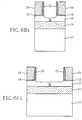
- FIGS. 6 Ai- 6 Ci and 6 Aii- 6 Ciiare pictorial representations (through cross sectional views) illustrating the structures of FIG. 5 after recessing the device channel;
- FIGS. 6 Ai- 6 Cishow that the shorter the channel length, the thinner the silicon film thickness.
- FIGS. 6 Aii- 6 Ciishow that the shorter the channel length, the thicker the silicon film.
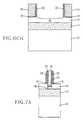
- FIGS. 7 A-Care pictorial representations (through cross sectional views) illustrating the structure of FIGS. 6 Ai- 6 Ci after gate formation and subsequent removal of the planarizing dielectric.
- FIGS. 8A-8Care pictorial representations (through cross sectional views) illustrating the structure of FIGS. 7A-7C after forming source/drain diffusion regions in the recessed Si device channel.
- FIG. 9is a plot of silicon thickness vs gate length.
- the initial SOI substrate 10includes a bottom Si-containing layer 12 , a buried insulating layer 14 , such as an oxide or nitride, located on the bottom Si-containing layer 12 , and a top Si-containing layer 16 , i.e., the SOI layer, located on the buried insulating layer 14 .
- the term “Si-containing layer”denotes any material that includes silicon.
- Si-containing materialsinclude, but are not limited to: Si, SiGe, SiGeC, SiC, polysilicon, i.e., polySi, epitaxial silicon, i.e., epi Si, amorphous silicon, i.e., a:Si, and multilayers thereof.
- layers 12 and 16 of the SOI substrate 10are both comprised of Si.
- the SOI layer 16 of the initial SOI substrate 10is typically, but not always, a doped layer, which may contain an n- or p-type dopant. Doping can be introduced into the SOI layer 16 prior to, or after formation of the SOI substrate 10 .
- the dopant concentration within the SOI layer 16is typically from about 1E17 to about 1E19 atoms/cm 3 .
- the SOI layer 16 of the SOI substrate 10may have a variable thickness, which is dependent on the technique that is used in forming the SOI substrate 10 .
- the top Si-containing layer 16 of the SOI substrate 10has a thickness from about 10 to about 1000 nm, with a thickness from about 50 to about 500 nm being more typical.
- the thickness of the buried insulating layer 14may also vary depending upon the technique used in fabricating the SOI substrate 10 .
- the buried insulating layer 14 of the present inventionhas a thickness from about 100 to about 1000 nm, with a buried insulating thickness from about 120 to about 200 nm being more typical.
- the thickness of the Si-containing substrate layer 12 of the SOI substrate 10is inconsequential to the present invention.
- the initial SOI substrate 10can be formed using a layer transfer process such as, a bonding process.
- a technique referred to as separation by implanted oxygen (SIMOX)wherein ions, typically oxygen or nitrogen, are implanted into a bulk Si-containing substrate and then the substrate containing the implanted ions is annealed under conditions that are capable of forming a buried insulating layer 14 can be employed.
- SIMOXseparation by implanted oxygen
- a pad oxide layer(not shown) is typically formed on an upper exposed surface of the SOI substrate 10 by a thermal oxidation process that is well known to those skilled in the art.
- the pad oxide layermay be formed by a deposition process, such as chemical vapor deposition (CVD), plasma-assisted chemical vapor deposition, evaporation or solution deposition.
- CVDchemical vapor deposition
- evaporation or solution depositionevaporation or solution deposition.
- the pad oxide layer formed at this point of the present inventiontypically has a thickness from about 5 to about 20 nm.
- isolation trench regionsare formed into the SOI substrate 10 by first forming a hardmask (not shown) in the surface of the pad oxide layer and then utilizing lithography and etching.
- the lithographic step employed in the present inventionincludes applying a photoresist (not shown) to the hardmask; exposing the photoresist to a pattern of radiation (in the present case a trench pattern is employed); and developing the pattern into the photoresist utilizing a conventional resist developer.
- the etching stepwhich is used to transfer the trench pattern first into the hardmask and then into the pad oxide layer and the SOI substrate 10 , includes any conventional dry etching process such as reactive-ion etching, ion beam etching, plasma etching, laser ablation or any combination thereof.
- a single etching processmay be employed, or alternatively, more than one etching process may be employed to form trenches in the SOI substrate 10 .
- the photoresistis typically removed from the structure and then pattern transfer continues using the hardmask as an etch mask.
- the depth of the trenches formedmay stop within the SOI layer 16 of the SOI substrate 10 , or it may extend down to the buried insulating layer 14 .
- the trenchesare filled with a trench dielectric material such as high-density plasma (HDP) oxide or TEOS (tetraethylorthosilicate) using conventional deposition processes well known to those skilled in the art.
- the filled trenchesform trench isolation regions in the structure that serve to isolate various device regions from each other.
- the walls of the trenchesare lined with a liner material, such as SiO 2 or Si 3 N 4 , prior to filling with the trench fill material.
- a conventional planarization process and/or densificationmay be performed on the structure.
- the planarization processstops on the hardmask and thereafter the hardmask is typically removed by utilizing an etching process that selectively removes the hardmask material from the structure.
- the pad oxide layeris removed from the surface of substrate 10 using a stripping process that is highly selective in removing oxide and thereafter sacrificial oxide layer 18 is formed on the SOI layer 16 of the SOI substrate 10 utilizing a conventional thermal oxidation process.
- the structure including the sacrificial oxide layer 18is shown, for example, in FIG. 2 .
- Sacrificial oxide layer 18 formed at this point of the inventive processtypically has a thickness from about 3 to about 20 nm, with a thickness from about 3 to about 6 nm being highly preferred. Note that the sacrificial oxide layer 18 is grown substantially over the Si-containing regions of the SOI substrate 10 , not atop trench isolation regions that may be formed therein.
- a dummy gate 20 comprising a sacrificial polysilicon region or other related materialis then formed on a portion of the sacrificial oxide layer 18 providing the structure also shown, for example, in FIG. 2
- the dummy gate 20is formed by first providing a sacrificial polysilicon layer or other related material atop the sacrificial oxide layer 18 utilizing a conventional deposition process such as CVD or PECVD.
- the sacrificial polysilicon layer or other related materialis then patterned by lithography and etching.
- FIG. 2also shows the structure after an outer insulating spacer 22 is formed on each sidewall of the dummy gate 20 .
- This step of forming the outer insulating spacer 22is optional.
- Outer insulating spacers 22which comprise a nitride, oxynitride or a combination thereof, are formed by deposition and etching. Outer insulating spacers 22 may have a variable thickness, but typically outer insulating spacers 22 have a thickness, as measured from a bottom surface, from about 10 to about 30 nm.
- the present inventionis not limited to forming just a single dummy gate 20 on the surface of the sacrificial oxide layer 18 . Instead, the present invention works equally well when a plurality of dummy gates 20 are formed. The formation of a plurality of dummy gates 20 will allow for the formation of a plurality of MOSFETs across the surface of the SOI substrate 10 . More than one outer insulating spacer is also contemplated herein.
- a planarizing material 24such as a high-density plasma (HDP) oxide or an oxide from tetraethylorthosilicate (TEOS) is deposited and planarized such that an upper surface of the planarizing material 24 is coplanar with an upper surface of the dummy gate 20 .
- HDPhigh-density plasma
- TEOStetraethylorthosilicate
- the dummy gate 20i.e., sacrificial polysilicon region or other related material, is removed from the structure using chemical downstream etching or KOH stopping atop the sacrificial oxide layer 18 .
- the resultant structurewhich includes a gate opening 25 that is formed after this step has been performed, is shown, for example, in FIG 3 .
- the inner edges 21 of the outer insulating spacers 22which define the boundaries of the gate opening 25 , also define the length G L of device channel 26 .
- the device channel 26is located in the SOI layer 16 .
- the device channel lengthcan be reduced by forming an inner insulating spacer (not shown) on each inner edge 21 of the outer insulating spacer 22 .
- the inner insulating spacermay be comprised of the same or different insulating material as the outer insulating spacer 22 .
- the inner insulating spacermay be used with, or without, the outer insulating spacer 22 .
- the inner spaceris used in defining the channel length.
- the inner spaceris formed by deposition and etching.
- Device channel (i.e., body region) 26may optionally be doped by utilizing an ion implantation step and an annealing step.
- the conditions used in forming the doped device channel 26are well known to those skilled in the art.
- the annealing stepserves to activate the dopants within the device channel 26 .
- the device channel 26may be ion implanted with a p-type dopant using any ion dosage such 1E12 to about 5E13 atoms/cm 2 and annealed at any conditions such as, for example, 1000° C., for 5 seconds in Ar.
- An n-type dopantis also contemplated herein.
- FIGS. 4A-4Cshow the ions 28 being implanted into the exposed SOI layer 16 for short, intermediate and long channel devices, respectively.
- reference numeral 29denotes the region of the SOI layer 16 that includes the implanted ions.
- the depth and concentration of the implanted ions as a function of channel lengthscan be designed by the implantation angle and the dummy gate height. There are more ions (nitrogen or fluorine) implanted in the SOI layer for longer channel devices. There are almost no ions implanted into the SOI layer for short channel devices due to the shadowing effect with angled implantation. Since oxidation is retarded (or enhanced) with the introduction of nitrogen (fluorine) implant, the recessed channel has a thinner (thicker) SOI film thickness for short channel lengths.
- the exposed sacrificial oxide 18 in the gate opening 25is then removed from the structure to expose the device channel 26 containing the implant region 29 .
- the exposed sacrificial oxide 18 in the gate openingis removed by utilizing a chemical oxide removal (COR) process.
- the COR process employed in the present inventionis carried out at relatively low pressures (6 millitorr or less) in a vapor, or more preferably, a plasma of HF and NH 3 .
- the HF and NH 3 mixtureis used as an etchant that selectively removes oxide from the structure.
- the resultant structure that is formed after the COR step has been performedis shown, for example, in FIGS. 5A-5C .
- the exposed SOI layer 16 containing the implant region 29is recessed, i.e., thinned, by utilizing an etching process that is capable of recessing, i.e., thinning the device channel 26 .
- an etching processthat is capable of recessing, i.e., thinning the device channel 26 .
- successive steps of oxidation and etching via a COR processing stepcan be used to selectively recess the exposed SOI layer 16 .
- FIGS. 6 Ai- 6 Cishow device structures with three different channel lengths after nitrogen implant and recessing. Because oxidation is retarded by the introduction of nitrogen ions, the recessed channel SOI film thickness is thicker for longer channel lengths.
- FIGS. 6 Aii- 6 Ciishow device structures with three different channel lengths after fluorine implantation and recessing. Because oxidation is enhanced by the introduction of implanted fluorine ions, the recessed channel SOI film is thinner for longer channel lengths. The fluorine implant process is appropriate for doped channel FDSOI MOSFETs.
- the recessed device channelis designated by reference numeral 26 in the drawings.
- the recessed device channel 26is an ultra thin body region of the SOI MOSFET structure.
- the recessed device channel 26 formed at this point of the present inventionhas a thickness of less than about 20 nm.
- gate dielectric 30is formed atop the exposed recessed device channel 26 utilizing a conventional deposition process.
- the gate dielectric 30may be formed by a thermal oxidation, nitridation or oxynitridation process. Combinations of the aforementioned processes may also be used in forming the gate dielectric 30 .
- the gate dielectric 30may be composed of any conventional dielectric including, but not limited to: SiO 2 ; Si 3 N 4 ; SiON; SiON 2 ; high-k dielectrics such as TiO 2 , Al 2 O 3 , ZrO 2 , HfO 2 , Ta 2 O 5 , La 2 O 3 ; and other like oxides including perovskite-type oxides. Typically, the high-k dielectrics are capable of withstanding high-temperature (900° C.) anneals. Gate dielectric 30 may also comprise any combination of the aforementioned dielectric materials.
- Gate dielectric 30is typically thinner than the sacrificial oxide layer 18 .
- the gate dielectric 30is composed of SiO 2 , Si 3 N 4 , SiON or SiON 2 , it has a thickness of about 1 to about 5 nm. For the other gate dielectrics, the thickness would provide an equivalent oxide thickness in the range mentioned above.
- a gate conductor 32which serves as the gate electrode of the MOSFET, is formed providing the structure shown in FIGS. 7A-7C .
- the gate dielectric and gate conductorare formed on the recessed device channel shown in FIG. 6A i- 6 Ci, respectively.
- the present inventionalso contemplates forming the gate dielectric and gate conducting on the recessed device channel depicted in FIGS. 6 Aii- 6 Cii.
- Gate conductor 32is comprised of a conductive material including, but not limited to: elemental metals such as W, Pt, Pd, Ru, Re, Ir, Ta, Mo or combinations and multilayers thereof; silicides or nitrides of the aforesaid elemental metals; polysilicon either doped or undoped; and any combinations thereof.
- the gate conductor 32is comprised of doped polysilicon.
- Gate conductor 32is formed utilizing a deposition process such as CVD, plasma-assisted CVD, sputtering, evaporation, chemical solution deposition and plating. When metal silicides are employed, a conventional silicidation process may be used in forming the same.
- the doped polysiliconmay be formed by an in-situ doping deposition process, or alternatively, a layer of undoped silicon is first deposited and thereafter an ion implantation process is employed in doping the undoped polysilicon. The doping of the undoped polysilicon may occur immediately after deposition or in a later processing step.
- gate conductor 32 formed at this point of the present inventionmay vary depending on the conductive material employed as well as the process used in forming the same. Typically, however, the gate conductor 32 has a thickness of from about 20 to about 400 nm, with a thickness of from about 50 to about 200 nm being more highly preferred.
- planarizing material 24is removed from the structure after gate formation using an etching process that is highly selective in removing oxide.
- an etching processthat is highly selective in removing oxide.
- KOH or an equivalent etchantcan be used to remove the planarizing material. Note that exposed portions of the sacrificial oxide layer 18 underlying the planarizing material 24 are also removed during this step.
- FIGS. 8A-8Cshow the structure after source/drain junctions (or regions) 34 are formed into the SOI layer 16 using a conventional angle implantation process followed by an annealing step.
- the implantis activated by annealing using conditions well known to those skilled in the art. For example, the implant may be annealed at 1000° C. for 1 second or longer.
- raised source/drain regionsmay be optionally formed atop the surface of the source/drain regions by epitaxially growing an epi Si layer thereon.
- salicide regionsmay be formed using a conventional salicidation process that includes, for example, forming a refractory metal such as Ti, Co or Ni on Si surfaces; heating the structure to form silicide regions and thereafter removing any non-reactive metal that was not converted into a silicide during the heating process.
- a salicide regionalso is formed thereon, unless appropriate steps (such as block mask formation) are taken to prevent the formation of a salicide region in the polysilicon gate conductor.
- BEOLback-end-of-the-line
- a layer of insulating materialsuch as BPSG (boron doped phosphorus silicate glass) can be formed over the structure by deposition and planarization.
- Contact openingscan be formed into the insulating layer by lithography and etching and thereafter the contact holes can be filled with a conductive material, such as, for example, Cu, Al, W, polysilicon and other like conductive materials.
- FIG. 9A device example based on device simulation is shown in FIG. 9 .
- constant threshold voltagecan be maintained provided that the SOI thickness is increased with the channel length according to the functional form shown in FIG. 9 .
Landscapes
- Thin Film Transistor (AREA)
Abstract
Description
- This application is a continuation application of U.S. Ser. No. 10/710,273, filed Jun. 30, 2004.
- The present invention relates to semiconductor integrated circuit devices as well as their fabrication, and more particularly to ultra thin body, e.g., channel, fully-depleted silicon-on-insulator (SOI) metal oxide semiconductor field effect transistor (MOSFET) devices in which the threshold voltage variation of each device is controlled.
- In semiconductor processing, silicon-on-insulator (SOI) technology is becoming increasingly important since it permits the formation of high-speed integrated circuits. In SOI technology, a buried insulating layer, especially a buried oxide, electrically isolates a top Si-containing layer from a bottom Si-containing substrate layer. The top Si-containing layer, which is oftentimes referred to in the art as the SOI layer, is generally the area in which active devices such as transistors are formed. Devices formed using SOI technology offer many advantages over the bulk counterparts including, for example, higher performance, absence of latch up, higher packing density and low voltage applications.
- In the semiconductor industry, the SOI layer thickness has been scaled down in every SOI device technology generation. Current technology trends are for providing SOI devices that have ultra thin Si channels. Ultra thin Si channel devices, which are formed in the SOI layer, have demonstrated excellent scalibity. The term “ultra thin” is used throughout the present application to denote a channel region having a vertical thickness of less than about 20 nm.
- It is also known that fully-depleted SOI MOSFET devices with doped channels typically have very large threshold voltage variations. The threshold voltage variations are effected by SOI thickness as well as well as the channel length variations that are a result of conventional device fabrication.
- In conventional fully-depleted SOI devices, the silicon film thickness is usually less than or equal to half the depletion width of the bulk device. The surface potentials at the front and back interfaces are strongly coupled to each other and capacitively coupled to the front-gate and substrate through the front-gate dielectric and the buried oxide, respectively. Therefore, the potential throughout the silicon film, and hence the charge, is determined by the bias conditions on both the front-gate and the substrate. The large variation in threshold voltage mentioned above has prevented fully-depleted SOI MOSFETs to become mainstream manufacturable complementary metal oxide semiconductor (CMOS) technology. Because of the current trends in reducing the SOI thickness, partially depleted SOI devices are being pushed closer and closer to the fully-depleted mode.
- SOI MOSFETs are often distinguished as partially depleted (PD) when the silicon film is thicker than the maximum gate depletion width, and fully developed (FD) when the silicon film is thin enough that the entire film is depleted before the threshold voltage condition is reached.
- In the prior art, halo implantation can be used to create a device in which the channel-length is dependent upon the total charge doping concentration. A well-designed halo implant can create devices such that the channel doping is higher in short channel devices. As a result, the threshold voltage vs. gate length curve can be flatten out. Therefore, devices can be operated at much shorter channel lengths. This prior art method however cannot be extended any further because 1) the junction leakage current could be to high with high halo doping concentration; and 2) the doping fluctuation effect could dominate the threshold variations in narrow width devices.
- In view of the prior art mentioned above, there is a need for providing a method of forming a fully-depleted SOI MOSFET device in which the threshold voltage variation with respect to SOI thickness and channel-length variations is minimized.
- The present invention provides a method of creating ultra thin body fully-depleted SOI MOSFETs in which the SOI thickness changes with gate-length variations thereby minimizing the threshold voltage variations that are typically caused by SOI thickness and gate-length variations. This object is achieved in the present invention by using a replacement gate process in which nitrogen (or fluorine) is implanted to selectively retard (enhance) oxidation during formation of a recessed channel. A self-limited chemical oxide removal (COR) processing step can be used to improve the control in the recessed channel step.
- If the channel is doped, the inventive method is designed such that the thickness of the SOI layer is increased with shorter channel lengths. If the channel is undoped or counter-doped, the inventive method is designed such that the thickness of the SOI layer is decreased with shorter channel lengths.
- In broad terms, the method of the present invention comprises the steps of:
- providing a SOI structure comprising a dummy gate that has an upper surface that is coplanar with an upper surface of a planarizing material, said dummy gate is located on a sacrificial oxide that is positioned atop a top Si-containing layer of a SOI substrate;
- removing the dummy gate to provide a gate opening that exposes a portion of the underlying sacrificial oxide layer, said gate opening defining a device channel in said top Si-containing layer;
- implanting nitrogen or fluorine ions into the device channel;
- removing the sacrificial oxide layer to expose the device channel;
- recessing the device channel to provide a recessed device channel; and
- forming the gate, including gate dielectric and gate electrode in said opening atop the recessed device channel.
- Following the gate forming step, the planarizing dielectric is etched back and source/drain diffusion regions can be formed utilizing ion implantation and annealing processing steps.
- In addition to the method described above, the present invention also contemplates the devices that are formed thereby. Specifically, the devices of the present invention comprise:
- a silicon-on-insulator (SOI) substrate having a SOI layer in which a first portion thereof has a thickness of less than about 20 nm;
- a gate including a gate dielectric and a gate electrode located atop the first portion of the SOI layer having said thickness; and
- source and drain diffusion regions located in a second portion of the SOI layer that is adjacent to said first portion, said second portion of the SOI layer is thicker than the first portion.
FIG. 1 is a pictorial representation (through a cross sectional view) illustrating an initial SOI substrate employed in the present invention.FIG. 2 is a pictorial representation (through a cross sectional view) illustrating the initial SOI substrate ofFIG. 1 after forming a dummy gate that has an upper surface that is coplanar with an upper surface of a planarizing material atop a sacrificial oxide layer that is formed on the SOI substrate.FIG. 3 is a pictorial representation (through a cross sectional view) illustrating the structure ofFIG. 2 after removing the dummy gate.FIGS. 4A-4C are pictorial representations (through cross sectional views) illustrating the structure ofFIG. 3 during ion implantation into the channel region; short, intermediate and long channel lengths, respectively, are shown.- FIGS.5A-C are pictorial representations (through cross sectional views) illustrating the structure of
FIG. 4 after removing the exposed sacrificial oxide layer; short, intermediate and long channel lengths, respectively, are shown. - FIGS.6Ai-6Ci and6Aii-6Cii are pictorial representations (through cross sectional views) illustrating the structures of
FIG. 5 after recessing the device channel; FIGS.6Ai-6Ci show that the shorter the channel length, the thinner the silicon film thickness. FIGS.6Aii-6Cii show that the shorter the channel length, the thicker the silicon film. - FIGS.7A-C are pictorial representations (through cross sectional views) illustrating the structure of FIGS.6Ai-6Ci after gate formation and subsequent removal of the planarizing dielectric.
FIGS. 8A-8C are pictorial representations (through cross sectional views) illustrating the structure ofFIGS. 7A-7C after forming source/drain diffusion regions in the recessed Si device channel.FIG. 9 is a plot of silicon thickness vs gate length.- The present invention, which provides a method for threshold voltage variations control in ultra thin fully-depleted SOI MOSFETs, will now be described in greater detail by referring to the drawings that accompany the present application.
- Referring to
FIG. 1 there is shown aninitial SOI substrate 10 that can be employed in the present invention. Theinitial SOI substrate 10 includes a bottom Si-containinglayer 12, a buried insulatinglayer 14, such as an oxide or nitride, located on the bottom Si-containinglayer 12, and a top Si-containinglayer 16, i.e., the SOI layer, located on the buried insulatinglayer 14. The term “Si-containing layer” denotes any material that includes silicon. Illustrative examples of Si-containing materials include, but are not limited to: Si, SiGe, SiGeC, SiC, polysilicon, i.e., polySi, epitaxial silicon, i.e., epi Si, amorphous silicon, i.e., a:Si, and multilayers thereof. Typically, layers12 and16 of theSOI substrate 10 are both comprised of Si. - The
SOI layer 16 of theinitial SOI substrate 10 is typically, but not always, a doped layer, which may contain an n- or p-type dopant. Doping can be introduced into theSOI layer 16 prior to, or after formation of theSOI substrate 10. The dopant concentration within theSOI layer 16 is typically from about 1E17 to about 1E19 atoms/cm3. - The
SOI layer 16 of theSOI substrate 10 may have a variable thickness, which is dependent on the technique that is used in forming theSOI substrate 10. Typically, however, the top Si-containinglayer 16 of theSOI substrate 10 has a thickness from about 10 to about 1000 nm, with a thickness from about 50 to about 500 nm being more typical. The thickness of the buried insulatinglayer 14 may also vary depending upon the technique used in fabricating theSOI substrate 10. Typically, however, the buried insulatinglayer 14 of the present invention has a thickness from about 100 to about 1000 nm, with a buried insulating thickness from about 120 to about 200 nm being more typical. The thickness of the Si-containingsubstrate layer 12 of theSOI substrate 10 is inconsequential to the present invention. - The
initial SOI substrate 10 can be formed using a layer transfer process such as, a bonding process. Alternatively, a technique referred to as separation by implanted oxygen (SIMOX) wherein ions, typically oxygen or nitrogen, are implanted into a bulk Si-containing substrate and then the substrate containing the implanted ions is annealed under conditions that are capable of forming a buried insulatinglayer 14 can be employed. - After providing the substrate, a pad oxide layer (not shown) is typically formed on an upper exposed surface of the
SOI substrate 10 by a thermal oxidation process that is well known to those skilled in the art. Alternatively, the pad oxide layer may be formed by a deposition process, such as chemical vapor deposition (CVD), plasma-assisted chemical vapor deposition, evaporation or solution deposition. The pad oxide layer formed at this point of the present invention typically has a thickness from about 5 to about 20 nm. - Next, isolation trench regions (not shown) are formed into the
SOI substrate 10 by first forming a hardmask (not shown) in the surface of the pad oxide layer and then utilizing lithography and etching. The lithographic step employed in the present invention includes applying a photoresist (not shown) to the hardmask; exposing the photoresist to a pattern of radiation (in the present case a trench pattern is employed); and developing the pattern into the photoresist utilizing a conventional resist developer. The etching step, which is used to transfer the trench pattern first into the hardmask and then into the pad oxide layer and theSOI substrate 10, includes any conventional dry etching process such as reactive-ion etching, ion beam etching, plasma etching, laser ablation or any combination thereof. A single etching process may be employed, or alternatively, more than one etching process may be employed to form trenches in theSOI substrate 10. After the pattern has been transferred into the hardmask, the photoresist is typically removed from the structure and then pattern transfer continues using the hardmask as an etch mask. The depth of the trenches formed may stop within theSOI layer 16 of theSOI substrate 10, or it may extend down to the buried insulatinglayer 14. - After trenches have been formed in the SOI substrate, the trenches are filled with a trench dielectric material such as high-density plasma (HDP) oxide or TEOS (tetraethylorthosilicate) using conventional deposition processes well known to those skilled in the art. The filled trenches form trench isolation regions in the structure that serve to isolate various device regions from each other. In some embodiments of the present invention, the walls of the trenches are lined with a liner material, such as SiO2or Si3N4, prior to filling with the trench fill material. After the filling process, a conventional planarization process and/or densification may be performed on the structure. The planarization process stops on the hardmask and thereafter the hardmask is typically removed by utilizing an etching process that selectively removes the hardmask material from the structure.
- Next, the pad oxide layer is removed from the surface of
substrate 10 using a stripping process that is highly selective in removing oxide and thereaftersacrificial oxide layer 18 is formed on theSOI layer 16 of theSOI substrate 10 utilizing a conventional thermal oxidation process. The structure including thesacrificial oxide layer 18 is shown, for example, inFIG. 2 .Sacrificial oxide layer 18 formed at this point of the inventive process typically has a thickness from about 3 to about 20 nm, with a thickness from about 3 to about 6 nm being highly preferred. Note that thesacrificial oxide layer 18 is grown substantially over the Si-containing regions of theSOI substrate 10, not atop trench isolation regions that may be formed therein. - A
dummy gate 20 comprising a sacrificial polysilicon region or other related material is then formed on a portion of thesacrificial oxide layer 18 providing the structure also shown, for example, inFIG. 2 Thedummy gate 20 is formed by first providing a sacrificial polysilicon layer or other related material atop thesacrificial oxide layer 18 utilizing a conventional deposition process such as CVD or PECVD. The sacrificial polysilicon layer or other related material is then patterned by lithography and etching. FIG. 2 also shows the structure after an outer insulatingspacer 22 is formed on each sidewall of thedummy gate 20. This step of forming the outer insulatingspacer 22 is optional. Outer insulatingspacers 22, which comprise a nitride, oxynitride or a combination thereof, are formed by deposition and etching. Outer insulatingspacers 22 may have a variable thickness, but typically outer insulatingspacers 22 have a thickness, as measured from a bottom surface, from about 10 to about 30 nm.- It should be noted that the present invention is not limited to forming just a
single dummy gate 20 on the surface of thesacrificial oxide layer 18. Instead, the present invention works equally well when a plurality ofdummy gates 20 are formed. The formation of a plurality ofdummy gates 20 will allow for the formation of a plurality of MOSFETs across the surface of theSOI substrate 10. More than one outer insulating spacer is also contemplated herein. - Next, and as also shown in
FIG. 2 , aplanarizing material 24 such as a high-density plasma (HDP) oxide or an oxide from tetraethylorthosilicate (TEOS) is deposited and planarized such that an upper surface of theplanarizing material 24 is coplanar with an upper surface of thedummy gate 20. - Next, the
dummy gate 20, i.e., sacrificial polysilicon region or other related material, is removed from the structure using chemical downstream etching or KOH stopping atop thesacrificial oxide layer 18. The resultant structure, which includes a gate opening25 that is formed after this step has been performed, is shown, for example, in FIG3. Note that theinner edges 21 of the outer insulatingspacers 22, which define the boundaries of the gate opening25, also define the length GLofdevice channel 26. As shown, thedevice channel 26 is located in theSOI layer 16. - If desired, the device channel length can be reduced by forming an inner insulating spacer (not shown) on each
inner edge 21 of the outer insulatingspacer 22. The inner insulating spacer may be comprised of the same or different insulating material as the outer insulatingspacer 22. The inner insulating spacer may be used with, or without, the outer insulatingspacer 22. In embodiments in which the outer spacer is not present, the inner spacer is used in defining the channel length. The inner spacer is formed by deposition and etching. - Device channel (i.e., body region)26 may optionally be doped by utilizing an ion implantation step and an annealing step. The conditions used in forming the
doped device channel 26 are well known to those skilled in the art. The annealing step serves to activate the dopants within thedevice channel 26. For example, thedevice channel 26 may be ion implanted with a p-type dopant using any ion dosage such 1E12 to about 5E13 atoms/cm2and annealed at any conditions such as, for example, 1000° C., for 5 seconds in Ar. An n-type dopant is also contemplated herein. - At this point of the present invention, ions such as nitrogen or fluorine are implanted into the device channel so as to modify the exposed
SOI layer 16 in such a way that the implanted region retards or enhances oxidation during the subsequent recessed channel processing step.FIGS. 4A-4C show theions 28 being implanted into the exposedSOI layer 16 for short, intermediate and long channel devices, respectively. InFIGS. 4A-4C ,reference numeral 29 denotes the region of theSOI layer 16 that includes the implanted ions. Although various doses of ions can be implanted, the ions are typically implanted using an ion dosage from about 5E13 to about 5E14 atoms/cm2. The depth and concentration of the implanted ions as a function of channel lengths can be designed by the implantation angle and the dummy gate height. There are more ions (nitrogen or fluorine) implanted in the SOI layer for longer channel devices. There are almost no ions implanted into the SOI layer for short channel devices due to the shadowing effect with angled implantation. Since oxidation is retarded (or enhanced) with the introduction of nitrogen (fluorine) implant, the recessed channel has a thinner (thicker) SOI film thickness for short channel lengths. - The exposed
sacrificial oxide 18 in the gate opening25 is then removed from the structure to expose thedevice channel 26 containing theimplant region 29. Specifically, the exposedsacrificial oxide 18 in the gate opening is removed by utilizing a chemical oxide removal (COR) process. The COR process employed in the present invention is carried out at relatively low pressures (6 millitorr or less) in a vapor, or more preferably, a plasma of HF and NH3. The HF and NH3mixture is used as an etchant that selectively removes oxide from the structure. The resultant structure that is formed after the COR step has been performed is shown, for example, inFIGS. 5A-5C . - Next, and as shown in FIGS.6Ai-6Ci and FIGS.6Aii-6Cii, the exposed
SOI layer 16 containing theimplant region 29 is recessed, i.e., thinned, by utilizing an etching process that is capable of recessing, i.e., thinning thedevice channel 26. For example, successive steps of oxidation and etching via a COR processing step can be used to selectively recess the exposedSOI layer 16. FIGS.6Ai-6Ci show device structures with three different channel lengths after nitrogen implant and recessing. Because oxidation is retarded by the introduction of nitrogen ions, the recessed channel SOI film thickness is thicker for longer channel lengths. This nitrogen implant process is appropriate for undoped (or counter doped) lengths. FIGS.6Aii-6Cii show device structures with three different channel lengths after fluorine implantation and recessing. Because oxidation is enhanced by the introduction of implanted fluorine ions, the recessed channel SOI film is thinner for longer channel lengths. The fluorine implant process is appropriate for doped channel FDSOI MOSFETs. - The recessed device channel is designated by
reference numeral 26 in the drawings. In accordance with the present invention, the recesseddevice channel 26 is an ultra thin body region of the SOI MOSFET structure. In particular, the recesseddevice channel 26 formed at this point of the present invention has a thickness of less than about 20 nm. - Next,
gate dielectric 30 is formed atop the exposed recesseddevice channel 26 utilizing a conventional deposition process. Alternatively, thegate dielectric 30 may be formed by a thermal oxidation, nitridation or oxynitridation process. Combinations of the aforementioned processes may also be used in forming thegate dielectric 30. Thegate dielectric 30 may be composed of any conventional dielectric including, but not limited to: SiO2; Si3N4; SiON; SiON2; high-k dielectrics such as TiO2, Al2O3, ZrO2, HfO2, Ta2O5, La2O3; and other like oxides including perovskite-type oxides. Typically, the high-k dielectrics are capable of withstanding high-temperature (900° C.) anneals.Gate dielectric 30 may also comprise any combination of the aforementioned dielectric materials. Gate dielectric 30 is typically thinner than thesacrificial oxide layer 18. Generally, when thegate dielectric 30 is composed of SiO2, Si3N4, SiON or SiON2, it has a thickness of about 1 to about 5 nm. For the other gate dielectrics, the thickness would provide an equivalent oxide thickness in the range mentioned above.- After forming the
gate dielectric 30 atop the recesseddevice channel 26, agate conductor 32, which serves as the gate electrode of the MOSFET, is formed providing the structure shown inFIGS. 7A-7C . Note that inFIGS. 7A-7C , the gate dielectric and gate conductor are formed on the recessed device channel shown inFIG. 6A i-6Ci, respectively. Although this embodiment is depicted, the present invention also contemplates forming the gate dielectric and gate conducting on the recessed device channel depicted in FIGS.6Aii-6Cii. Gate conductor 32 is comprised of a conductive material including, but not limited to: elemental metals such as W, Pt, Pd, Ru, Re, Ir, Ta, Mo or combinations and multilayers thereof; silicides or nitrides of the aforesaid elemental metals; polysilicon either doped or undoped; and any combinations thereof. Typically, thegate conductor 32 is comprised of doped polysilicon.Gate conductor 32 is formed utilizing a deposition process such as CVD, plasma-assisted CVD, sputtering, evaporation, chemical solution deposition and plating. When metal silicides are employed, a conventional silicidation process may be used in forming the same. On the other hand, when doped polysilicon is employed as thegate conductor 32, the doped polysilicon may be formed by an in-situ doping deposition process, or alternatively, a layer of undoped silicon is first deposited and thereafter an ion implantation process is employed in doping the undoped polysilicon. The doping of the undoped polysilicon may occur immediately after deposition or in a later processing step.- The physical thickness of
gate conductor 32 formed at this point of the present invention may vary depending on the conductive material employed as well as the process used in forming the same. Typically, however, thegate conductor 32 has a thickness of from about 20 to about 400 nm, with a thickness of from about 50 to about 200 nm being more highly preferred. - Reference is still made to the structures shown in
FIGS. 7A-7C in which theplanarizing material 24 is removed from the structure after gate formation using an etching process that is highly selective in removing oxide. For example, KOH or an equivalent etchant can be used to remove the planarizing material. Note that exposed portions of thesacrificial oxide layer 18 underlying theplanarizing material 24 are also removed during this step. FIGS. 8A-8C show the structure after source/drain junctions (or regions)34 are formed into theSOI layer 16 using a conventional angle implantation process followed by an annealing step. The implant is activated by annealing using conditions well known to those skilled in the art. For example, the implant may be annealed at 1000° C. for 1 second or longer.- At this point of the present invention, raised source/drain regions (not shown) may be optionally formed atop the surface of the source/drain regions by epitaxially growing an epi Si layer thereon. To either the raised source/drain regions or to the previously formed source/
drain regions 34, salicide regions (not shown) may be formed using a conventional salicidation process that includes, for example, forming a refractory metal such as Ti, Co or Ni on Si surfaces; heating the structure to form silicide regions and thereafter removing any non-reactive metal that was not converted into a silicide during the heating process. In embodiments in which thegate conductor 32 is comprised of polySi, a salicide region also is formed thereon, unless appropriate steps (such as block mask formation) are taken to prevent the formation of a salicide region in the polysilicon gate conductor. - Further BEOL (back-end-of-the-line) processes may be formed on the structure shown in
FIGS. 8A-8C . For example, a layer of insulating material such as BPSG (boron doped phosphorus silicate glass) can be formed over the structure by deposition and planarization. Contact openings can be formed into the insulating layer by lithography and etching and thereafter the contact holes can be filled with a conductive material, such as, for example, Cu, Al, W, polysilicon and other like conductive materials. - A device example based on device simulation is shown in
FIG. 9 . For high channel doping, constant threshold voltage can be maintained provided that the SOI thickness is increased with the channel length according to the functional form shown inFIG. 9 . - While the present invention has been particularly shown and described with respect to preferred embodiments thereof, it will be understood by one skilled in the art that the foregoing and other changes in form and detail may be made without departing from the spirit and scope of the present invention. It is therefore intended that the present invention not be limited to the exact forms and details described and illustrated, but fall within the scope of the appended claims.
Claims (14)
Priority Applications (1)
| Application Number | Priority Date | Filing Date | Title |
|---|---|---|---|
| US11/473,757US7459752B2 (en) | 2004-06-30 | 2006-06-23 | Ultra thin body fully-depleted SOI MOSFETs |
Applications Claiming Priority (2)
| Application Number | Priority Date | Filing Date | Title |
|---|---|---|---|
| US10/710,273US7091069B2 (en) | 2004-06-30 | 2004-06-30 | Ultra thin body fully-depleted SOI MOSFETs |
| US11/473,757US7459752B2 (en) | 2004-06-30 | 2006-06-23 | Ultra thin body fully-depleted SOI MOSFETs |
Related Parent Applications (1)
| Application Number | Title | Priority Date | Filing Date |
|---|---|---|---|
| US10/710,273ContinuationUS7091069B2 (en) | 2004-06-30 | 2004-06-30 | Ultra thin body fully-depleted SOI MOSFETs |
Publications (2)
| Publication Number | Publication Date |
|---|---|
| US20060237791A1true US20060237791A1 (en) | 2006-10-26 |
| US7459752B2 US7459752B2 (en) | 2008-12-02 |
Family
ID=35513000
Family Applications (2)
| Application Number | Title | Priority Date | Filing Date |
|---|---|---|---|
| US10/710,273Expired - Fee RelatedUS7091069B2 (en) | 2004-06-30 | 2004-06-30 | Ultra thin body fully-depleted SOI MOSFETs |
| US11/473,757Expired - LifetimeUS7459752B2 (en) | 2004-06-30 | 2006-06-23 | Ultra thin body fully-depleted SOI MOSFETs |
Family Applications Before (1)
| Application Number | Title | Priority Date | Filing Date |
|---|---|---|---|
| US10/710,273Expired - Fee RelatedUS7091069B2 (en) | 2004-06-30 | 2004-06-30 | Ultra thin body fully-depleted SOI MOSFETs |
Country Status (1)
| Country | Link |
|---|---|
| US (2) | US7091069B2 (en) |
Cited By (9)
| Publication number | Priority date | Publication date | Assignee | Title |
|---|---|---|---|---|
| US7355249B2 (en)* | 2005-04-28 | 2008-04-08 | International Business Machines Corporation | Silicon-on-insulator based radiation detection device and method |
| US20110278673A1 (en)* | 2010-05-13 | 2011-11-17 | International Business Machines Corporation | Methodology for fabricating isotropically recessed source and drain regions of cmos transistors |
| CN103003940A (en)* | 2009-10-12 | 2013-03-27 | 莫诺利特斯3D<sup>TM</sup>有限公司 | System with semiconductor device and structure |
| US8569158B2 (en) | 2011-03-31 | 2013-10-29 | Tokyo Electron Limited | Method for forming ultra-shallow doping regions by solid phase diffusion |
| US8580664B2 (en) | 2011-03-31 | 2013-11-12 | Tokyo Electron Limited | Method for forming ultra-shallow boron doping regions by solid phase diffusion |
| US8617956B2 (en) | 2010-08-19 | 2013-12-31 | International Business Machines Corporation | Method and structure for forming high-K/metal gate extremely thin semiconductor on insulator device |
| US20140175513A1 (en)* | 2012-12-21 | 2014-06-26 | Taiwan Semiconductor Manufacturing Company, Ltd. | Structure And Method For Integrated Devices On Different Substartes With Interfacial Engineering |
| US20150041904A1 (en)* | 2011-11-04 | 2015-02-12 | International Business Machines Corporation | Blanket short channel roll-up implant with non-angled long channel compensating implant through patterned opening |
| US9899224B2 (en) | 2015-03-03 | 2018-02-20 | Tokyo Electron Limited | Method of controlling solid phase diffusion of boron dopants to form ultra-shallow doping regions |
Families Citing this family (276)
| Publication number | Priority date | Publication date | Assignee | Title |
|---|---|---|---|---|
| JP3651802B2 (en)* | 2002-09-12 | 2005-05-25 | 株式会社東芝 | Manufacturing method of semiconductor device |
| WO2006036934A2 (en)* | 2004-09-27 | 2006-04-06 | Ball Corporation | Container end closure |
| US7518196B2 (en) | 2005-02-23 | 2009-04-14 | Intel Corporation | Field effect transistor with narrow bandgap source and drain regions and method of fabrication |
| US7858481B2 (en) | 2005-06-15 | 2010-12-28 | Intel Corporation | Method for fabricating transistor with thinned channel |
| US7547637B2 (en) | 2005-06-21 | 2009-06-16 | Intel Corporation | Methods for patterning a semiconductor film |
| JP4967264B2 (en)* | 2005-07-11 | 2012-07-04 | 株式会社日立製作所 | Semiconductor device |
| JP2007220718A (en)* | 2006-02-14 | 2007-08-30 | Toyota Motor Corp | Semiconductor substrate, method for manufacturing the same, and semiconductor device |
| JP2007281280A (en)* | 2006-04-10 | 2007-10-25 | Toshiba Corp | Semiconductor device and manufacturing method thereof |
| US7485510B2 (en)* | 2006-10-03 | 2009-02-03 | International Business Machines Corporation | Field effect device including inverted V shaped channel region and method for fabrication thereof |
| US7659579B2 (en) | 2006-10-06 | 2010-02-09 | International Business Machines Corporation | FETS with self-aligned bodies and backgate holes |
| US7446007B2 (en) | 2006-11-17 | 2008-11-04 | International Business Machines Corporation | Multi-layer spacer with inhibited recess/undercut and method for fabrication thereof |
| US7786016B2 (en)* | 2007-01-11 | 2010-08-31 | Micron Technology, Inc. | Methods of uniformly removing silicon oxide and a method of removing a sacrificial oxide |
| US20080191788A1 (en)* | 2007-02-08 | 2008-08-14 | International Business Machines Corporation | Soi mosfet device with adjustable threshold voltage |
| US7659155B2 (en)* | 2007-03-08 | 2010-02-09 | International Business Machines Corporation | Method of forming a transistor having gate and body in direct self-aligned contact |
| EP2174122A2 (en)* | 2007-06-08 | 2010-04-14 | Bharath R Takulapalli | Nano structured field effect sensor and methods of forming and using same |
| US7937675B2 (en)* | 2007-11-06 | 2011-05-03 | International Business Machines Corporation | Structure including transistor having gate and body in direct self-aligned contact |
| US8252194B2 (en)* | 2008-05-02 | 2012-08-28 | Micron Technology, Inc. | Methods of removing silicon oxide |
| KR20100047558A (en)* | 2008-10-29 | 2010-05-10 | 삼성전자주식회사 | Semiconductor devices and methods of formign the same |
| US7883944B2 (en)* | 2009-03-19 | 2011-02-08 | International Business Machines Corporation | Ultra-thin semiconductor on insulator metal gate complementary field effect transistor with metal gate and method of forming thereof |
| US9509313B2 (en) | 2009-04-14 | 2016-11-29 | Monolithic 3D Inc. | 3D semiconductor device |
| US8405420B2 (en) | 2009-04-14 | 2013-03-26 | Monolithic 3D Inc. | System comprising a semiconductor device and structure |
| US9577642B2 (en) | 2009-04-14 | 2017-02-21 | Monolithic 3D Inc. | Method to form a 3D semiconductor device |
| US8362800B2 (en) | 2010-10-13 | 2013-01-29 | Monolithic 3D Inc. | 3D semiconductor device including field repairable logics |
| US9711407B2 (en) | 2009-04-14 | 2017-07-18 | Monolithic 3D Inc. | Method of manufacturing a three dimensional integrated circuit by transfer of a mono-crystalline layer |
| US8373439B2 (en) | 2009-04-14 | 2013-02-12 | Monolithic 3D Inc. | 3D semiconductor device |
| US8384426B2 (en) | 2009-04-14 | 2013-02-26 | Monolithic 3D Inc. | Semiconductor device and structure |
| US8378715B2 (en) | 2009-04-14 | 2013-02-19 | Monolithic 3D Inc. | Method to construct systems |
| US8362482B2 (en) | 2009-04-14 | 2013-01-29 | Monolithic 3D Inc. | Semiconductor device and structure |
| US8258810B2 (en) | 2010-09-30 | 2012-09-04 | Monolithic 3D Inc. | 3D semiconductor device |
| US7986042B2 (en) | 2009-04-14 | 2011-07-26 | Monolithic 3D Inc. | Method for fabrication of a semiconductor device and structure |
| US8058137B1 (en) | 2009-04-14 | 2011-11-15 | Monolithic 3D Inc. | Method for fabrication of a semiconductor device and structure |
| US8669778B1 (en) | 2009-04-14 | 2014-03-11 | Monolithic 3D Inc. | Method for design and manufacturing of a 3D semiconductor device |
| US8427200B2 (en) | 2009-04-14 | 2013-04-23 | Monolithic 3D Inc. | 3D semiconductor device |
| US8754533B2 (en) | 2009-04-14 | 2014-06-17 | Monolithic 3D Inc. | Monolithic three-dimensional semiconductor device and structure |
| US10157909B2 (en) | 2009-10-12 | 2018-12-18 | Monolithic 3D Inc. | 3D semiconductor device and structure |
| US10366970B2 (en) | 2009-10-12 | 2019-07-30 | Monolithic 3D Inc. | 3D semiconductor device and structure |
| US10388863B2 (en) | 2009-10-12 | 2019-08-20 | Monolithic 3D Inc. | 3D memory device and structure |
| US11018133B2 (en) | 2009-10-12 | 2021-05-25 | Monolithic 3D Inc. | 3D integrated circuit |
| US8536023B2 (en) | 2010-11-22 | 2013-09-17 | Monolithic 3D Inc. | Method of manufacturing a semiconductor device and structure |
| US10043781B2 (en) | 2009-10-12 | 2018-08-07 | Monolithic 3D Inc. | 3D semiconductor device and structure |
| US8476145B2 (en) | 2010-10-13 | 2013-07-02 | Monolithic 3D Inc. | Method of fabricating a semiconductor device and structure |
| US10354995B2 (en) | 2009-10-12 | 2019-07-16 | Monolithic 3D Inc. | Semiconductor memory device and structure |
| US10910364B2 (en) | 2009-10-12 | 2021-02-02 | Monolitaic 3D Inc. | 3D semiconductor device |
| US8148728B2 (en) | 2009-10-12 | 2012-04-03 | Monolithic 3D, Inc. | Method for fabrication of a semiconductor device and structure |
| US12027518B1 (en) | 2009-10-12 | 2024-07-02 | Monolithic 3D Inc. | 3D semiconductor devices and structures with metal layers |
| US11374118B2 (en) | 2009-10-12 | 2022-06-28 | Monolithic 3D Inc. | Method to form a 3D integrated circuit |
| US8581349B1 (en) | 2011-05-02 | 2013-11-12 | Monolithic 3D Inc. | 3D memory semiconductor device and structure |
| US9099424B1 (en) | 2012-08-10 | 2015-08-04 | Monolithic 3D Inc. | Semiconductor system, device and structure with heat removal |
| US11984445B2 (en) | 2009-10-12 | 2024-05-14 | Monolithic 3D Inc. | 3D semiconductor devices and structures with metal layers |
| US8742476B1 (en) | 2012-11-27 | 2014-06-03 | Monolithic 3D Inc. | Semiconductor device and structure |
| US8450804B2 (en) | 2011-03-06 | 2013-05-28 | Monolithic 3D Inc. | Semiconductor device and structure for heat removal |
| US8026521B1 (en) | 2010-10-11 | 2011-09-27 | Monolithic 3D Inc. | Semiconductor device and structure |
| US8492886B2 (en) | 2010-02-16 | 2013-07-23 | Monolithic 3D Inc | 3D integrated circuit with logic |
| US8461035B1 (en) | 2010-09-30 | 2013-06-11 | Monolithic 3D Inc. | Method for fabrication of a semiconductor device and structure |
| US8541819B1 (en) | 2010-12-09 | 2013-09-24 | Monolithic 3D Inc. | Semiconductor device and structure |
| US8298875B1 (en) | 2011-03-06 | 2012-10-30 | Monolithic 3D Inc. | Method for fabrication of a semiconductor device and structure |
| US9099526B2 (en) | 2010-02-16 | 2015-08-04 | Monolithic 3D Inc. | Integrated circuit device and structure |
| US8373230B1 (en) | 2010-10-13 | 2013-02-12 | Monolithic 3D Inc. | Method for fabrication of a semiconductor device and structure |
| US8283217B2 (en)* | 2010-03-04 | 2012-10-09 | International Business Machines Corporation | Prevention of oxygen absorption into high-K gate dielectric of silicon-on-insulator based finFET devices |
| US9953925B2 (en) | 2011-06-28 | 2018-04-24 | Monolithic 3D Inc. | Semiconductor system and device |
| US9219005B2 (en) | 2011-06-28 | 2015-12-22 | Monolithic 3D Inc. | Semiconductor system and device |
| US8901613B2 (en) | 2011-03-06 | 2014-12-02 | Monolithic 3D Inc. | Semiconductor device and structure for heat removal |
| US8642416B2 (en) | 2010-07-30 | 2014-02-04 | Monolithic 3D Inc. | Method of forming three dimensional integrated circuit devices using layer transfer technique |
| US10217667B2 (en) | 2011-06-28 | 2019-02-26 | Monolithic 3D Inc. | 3D semiconductor device, fabrication method and system |
| US12362219B2 (en) | 2010-11-18 | 2025-07-15 | Monolithic 3D Inc. | 3D semiconductor memory device and structure |
| US8163581B1 (en) | 2010-10-13 | 2012-04-24 | Monolith IC 3D | Semiconductor and optoelectronic devices |
| US8273610B2 (en) | 2010-11-18 | 2012-09-25 | Monolithic 3D Inc. | Method of constructing a semiconductor device and structure |
| US10497713B2 (en) | 2010-11-18 | 2019-12-03 | Monolithic 3D Inc. | 3D semiconductor memory device and structure |
| US11482440B2 (en) | 2010-12-16 | 2022-10-25 | Monolithic 3D Inc. | 3D semiconductor device and structure with a built-in test circuit for repairing faulty circuits |
| US11158674B2 (en) | 2010-10-11 | 2021-10-26 | Monolithic 3D Inc. | Method to produce a 3D semiconductor device and structure |
| US11018191B1 (en) | 2010-10-11 | 2021-05-25 | Monolithic 3D Inc. | 3D semiconductor device and structure |
| US11469271B2 (en) | 2010-10-11 | 2022-10-11 | Monolithic 3D Inc. | Method to produce 3D semiconductor devices and structures with memory |
| US11600667B1 (en) | 2010-10-11 | 2023-03-07 | Monolithic 3D Inc. | Method to produce 3D semiconductor devices and structures with memory |
| US11227897B2 (en) | 2010-10-11 | 2022-01-18 | Monolithic 3D Inc. | Method for producing a 3D semiconductor memory device and structure |
| US10896931B1 (en) | 2010-10-11 | 2021-01-19 | Monolithic 3D Inc. | 3D semiconductor device and structure |
| US11257867B1 (en) | 2010-10-11 | 2022-02-22 | Monolithic 3D Inc. | 3D semiconductor device and structure with oxide bonds |
| US11315980B1 (en) | 2010-10-11 | 2022-04-26 | Monolithic 3D Inc. | 3D semiconductor device and structure with transistors |
| US8114757B1 (en) | 2010-10-11 | 2012-02-14 | Monolithic 3D Inc. | Semiconductor device and structure |
| US10290682B2 (en) | 2010-10-11 | 2019-05-14 | Monolithic 3D Inc. | 3D IC semiconductor device and structure with stacked memory |
| US11024673B1 (en) | 2010-10-11 | 2021-06-01 | Monolithic 3D Inc. | 3D semiconductor device and structure |
| US11404466B2 (en) | 2010-10-13 | 2022-08-02 | Monolithic 3D Inc. | Multilevel semiconductor device and structure with image sensors |
| US10998374B1 (en) | 2010-10-13 | 2021-05-04 | Monolithic 3D Inc. | Multilevel semiconductor device and structure |
| US12080743B2 (en) | 2010-10-13 | 2024-09-03 | Monolithic 3D Inc. | Multilevel semiconductor device and structure with image sensors and wafer bonding |
| US11063071B1 (en) | 2010-10-13 | 2021-07-13 | Monolithic 3D Inc. | Multilevel semiconductor device and structure with waveguides |
| US11327227B2 (en) | 2010-10-13 | 2022-05-10 | Monolithic 3D Inc. | Multilevel semiconductor device and structure with electromagnetic modulators |
| US9197804B1 (en) | 2011-10-14 | 2015-11-24 | Monolithic 3D Inc. | Semiconductor and optoelectronic devices |
| US11869915B2 (en) | 2010-10-13 | 2024-01-09 | Monolithic 3D Inc. | Multilevel semiconductor device and structure with image sensors and wafer bonding |
| US11043523B1 (en) | 2010-10-13 | 2021-06-22 | Monolithic 3D Inc. | Multilevel semiconductor device and structure with image sensors |
| US8379458B1 (en) | 2010-10-13 | 2013-02-19 | Monolithic 3D Inc. | Semiconductor device and structure |
| US8283215B2 (en)* | 2010-10-13 | 2012-10-09 | Monolithic 3D Inc. | Semiconductor and optoelectronic devices |
| US11855114B2 (en) | 2010-10-13 | 2023-12-26 | Monolithic 3D Inc. | Multilevel semiconductor device and structure with image sensors and wafer bonding |
| US11163112B2 (en) | 2010-10-13 | 2021-11-02 | Monolithic 3D Inc. | Multilevel semiconductor device and structure with electromagnetic modulators |
| US11984438B2 (en) | 2010-10-13 | 2024-05-14 | Monolithic 3D Inc. | Multilevel semiconductor device and structure with oxide bonding |
| US11929372B2 (en) | 2010-10-13 | 2024-03-12 | Monolithic 3D Inc. | Multilevel semiconductor device and structure with image sensors and wafer bonding |
| US10943934B2 (en) | 2010-10-13 | 2021-03-09 | Monolithic 3D Inc. | Multilevel semiconductor device and structure |
| US11855100B2 (en) | 2010-10-13 | 2023-12-26 | Monolithic 3D Inc. | Multilevel semiconductor device and structure with oxide bonding |
| US11133344B2 (en) | 2010-10-13 | 2021-09-28 | Monolithic 3D Inc. | Multilevel semiconductor device and structure with image sensors |
| US10978501B1 (en) | 2010-10-13 | 2021-04-13 | Monolithic 3D Inc. | Multilevel semiconductor device and structure with waveguides |
| US10833108B2 (en) | 2010-10-13 | 2020-11-10 | Monolithic 3D Inc. | 3D microdisplay device and structure |
| US11694922B2 (en) | 2010-10-13 | 2023-07-04 | Monolithic 3D Inc. | Multilevel semiconductor device and structure with oxide bonding |
| US11437368B2 (en) | 2010-10-13 | 2022-09-06 | Monolithic 3D Inc. | Multilevel semiconductor device and structure with oxide bonding |
| US12360310B2 (en) | 2010-10-13 | 2025-07-15 | Monolithic 3D Inc. | Multilevel semiconductor device and structure with oxide bonding |
| US10679977B2 (en) | 2010-10-13 | 2020-06-09 | Monolithic 3D Inc. | 3D microdisplay device and structure |
| US12094892B2 (en) | 2010-10-13 | 2024-09-17 | Monolithic 3D Inc. | 3D micro display device and structure |
| US11164898B2 (en) | 2010-10-13 | 2021-11-02 | Monolithic 3D Inc. | Multilevel semiconductor device and structure |
| US11605663B2 (en) | 2010-10-13 | 2023-03-14 | Monolithic 3D Inc. | Multilevel semiconductor device and structure with image sensors and wafer bonding |
| US9698054B2 (en) | 2010-10-19 | 2017-07-04 | Taiwan Semiconductor Manufacturing Company, Ltd. | Strained structure of a p-type field effect transistor |
| US11610802B2 (en) | 2010-11-18 | 2023-03-21 | Monolithic 3D Inc. | Method for producing a 3D semiconductor device and structure with single crystal transistors and metal gate electrodes |
| US11569117B2 (en) | 2010-11-18 | 2023-01-31 | Monolithic 3D Inc. | 3D semiconductor device and structure with single-crystal layers |
| US11355380B2 (en) | 2010-11-18 | 2022-06-07 | Monolithic 3D Inc. | Methods for producing 3D semiconductor memory device and structure utilizing alignment marks |
| US11121021B2 (en) | 2010-11-18 | 2021-09-14 | Monolithic 3D Inc. | 3D semiconductor device and structure |
| US11482438B2 (en) | 2010-11-18 | 2022-10-25 | Monolithic 3D Inc. | Methods for producing a 3D semiconductor memory device and structure |
| US12272586B2 (en) | 2010-11-18 | 2025-04-08 | Monolithic 3D Inc. | 3D semiconductor memory device and structure with memory and metal layers |
| US12144190B2 (en) | 2010-11-18 | 2024-11-12 | Monolithic 3D Inc. | 3D semiconductor device and structure with bonding and memory cells preliminary class |
| US11004719B1 (en) | 2010-11-18 | 2021-05-11 | Monolithic 3D Inc. | Methods for producing a 3D semiconductor memory device and structure |
| US11508605B2 (en) | 2010-11-18 | 2022-11-22 | Monolithic 3D Inc. | 3D semiconductor memory device and structure |
| US11107721B2 (en) | 2010-11-18 | 2021-08-31 | Monolithic 3D Inc. | 3D semiconductor device and structure with NAND logic |
| US11901210B2 (en) | 2010-11-18 | 2024-02-13 | Monolithic 3D Inc. | 3D semiconductor device and structure with memory |
| US11443971B2 (en) | 2010-11-18 | 2022-09-13 | Monolithic 3D Inc. | 3D semiconductor device and structure with memory |
| US11482439B2 (en) | 2010-11-18 | 2022-10-25 | Monolithic 3D Inc. | Methods for producing a 3D semiconductor memory device comprising charge trap junction-less transistors |
| US11211279B2 (en) | 2010-11-18 | 2021-12-28 | Monolithic 3D Inc. | Method for processing a 3D integrated circuit and structure |
| US11355381B2 (en) | 2010-11-18 | 2022-06-07 | Monolithic 3D Inc. | 3D semiconductor memory device and structure |
| US11784082B2 (en) | 2010-11-18 | 2023-10-10 | Monolithic 3D Inc. | 3D semiconductor device and structure with bonding |
| US11735462B2 (en) | 2010-11-18 | 2023-08-22 | Monolithic 3D Inc. | 3D semiconductor device and structure with single-crystal layers |
| US11031275B2 (en) | 2010-11-18 | 2021-06-08 | Monolithic 3D Inc. | 3D semiconductor device and structure with memory |
| US11094576B1 (en) | 2010-11-18 | 2021-08-17 | Monolithic 3D Inc. | Methods for producing a 3D semiconductor memory device and structure |
| US11521888B2 (en) | 2010-11-18 | 2022-12-06 | Monolithic 3D Inc. | 3D semiconductor device and structure with high-k metal gate transistors |
| US12125737B1 (en) | 2010-11-18 | 2024-10-22 | Monolithic 3D Inc. | 3D semiconductor device and structure with metal layers and memory cells |
| US12136562B2 (en) | 2010-11-18 | 2024-11-05 | Monolithic 3D Inc. | 3D semiconductor device and structure with single-crystal layers |
| US11854857B1 (en) | 2010-11-18 | 2023-12-26 | Monolithic 3D Inc. | Methods for producing a 3D semiconductor device and structure with memory cells and multiple metal layers |
| US11615977B2 (en) | 2010-11-18 | 2023-03-28 | Monolithic 3D Inc. | 3D semiconductor memory device and structure |
| US11804396B2 (en) | 2010-11-18 | 2023-10-31 | Monolithic 3D Inc. | Methods for producing a 3D semiconductor device and structure with memory cells and multiple metal layers |
| US12068187B2 (en) | 2010-11-18 | 2024-08-20 | Monolithic 3D Inc. | 3D semiconductor device and structure with bonding and DRAM memory cells |
| US12033884B2 (en) | 2010-11-18 | 2024-07-09 | Monolithic 3D Inc. | Methods for producing a 3D semiconductor device and structure with memory cells and multiple metal layers |
| US11495484B2 (en) | 2010-11-18 | 2022-11-08 | Monolithic 3D Inc. | 3D semiconductor devices and structures with at least two single-crystal layers |
| US11923230B1 (en) | 2010-11-18 | 2024-03-05 | Monolithic 3D Inc. | 3D semiconductor device and structure with bonding |
| US11164770B1 (en) | 2010-11-18 | 2021-11-02 | Monolithic 3D Inc. | Method for producing a 3D semiconductor memory device and structure |
| US12243765B2 (en) | 2010-11-18 | 2025-03-04 | Monolithic 3D Inc. | 3D semiconductor device and structure with metal layers and memory cells |
| US11862503B2 (en) | 2010-11-18 | 2024-01-02 | Monolithic 3D Inc. | Method for producing a 3D semiconductor device and structure with memory cells and multiple metal layers |
| US12154817B1 (en) | 2010-11-18 | 2024-11-26 | Monolithic 3D Inc. | Methods for producing a 3D semiconductor memory device and structure |
| US12100611B2 (en) | 2010-11-18 | 2024-09-24 | Monolithic 3D Inc. | Methods for producing a 3D semiconductor device and structure with memory cells and multiple metal layers |
| US11018042B1 (en) | 2010-11-18 | 2021-05-25 | Monolithic 3D Inc. | 3D semiconductor memory device and structure |
| US8975670B2 (en) | 2011-03-06 | 2015-03-10 | Monolithic 3D Inc. | Semiconductor device and structure for heat removal |
| FR2972564B1 (en)* | 2011-03-08 | 2016-11-04 | S O I Tec Silicon On Insulator Tech | METHOD FOR PROCESSING A SEMICONDUCTOR TYPE STRUCTURE ON INSULATION |
| US8211775B1 (en) | 2011-03-09 | 2012-07-03 | United Microelectronics Corp. | Method of making transistor having metal gate |
| US8519487B2 (en) | 2011-03-21 | 2013-08-27 | United Microelectronics Corp. | Semiconductor device |
| US8691650B2 (en)* | 2011-04-14 | 2014-04-08 | International Business Machines Corporation | MOSFET with recessed channel film and abrupt junctions |
| KR20120133652A (en)* | 2011-05-31 | 2012-12-11 | 삼성전자주식회사 | Method for manufacturing semiconductor device |
| US8765561B2 (en) | 2011-06-06 | 2014-07-01 | United Microelectronics Corp. | Method for fabricating semiconductor device |
| US10388568B2 (en) | 2011-06-28 | 2019-08-20 | Monolithic 3D Inc. | 3D semiconductor device and system |
| US8921944B2 (en) | 2011-07-19 | 2014-12-30 | United Microelectronics Corp. | Semiconductor device |
| US8647941B2 (en) | 2011-08-17 | 2014-02-11 | United Microelectronics Corp. | Method of forming semiconductor device |
| US8994123B2 (en) | 2011-08-22 | 2015-03-31 | Gold Standard Simulations Ltd. | Variation resistant metal-oxide-semiconductor field effect transistor (MOSFET) |
| US8687399B2 (en) | 2011-10-02 | 2014-04-01 | Monolithic 3D Inc. | Semiconductor device and structure |
| US9029173B2 (en) | 2011-10-18 | 2015-05-12 | Monolithic 3D Inc. | Method for fabrication of a semiconductor device and structure |
| US8691659B2 (en) | 2011-10-26 | 2014-04-08 | United Microelectronics Corp. | Method for forming void-free dielectric layer |
| US9000557B2 (en) | 2012-03-17 | 2015-04-07 | Zvi Or-Bach | Semiconductor device and structure |
| US9373684B2 (en) | 2012-03-20 | 2016-06-21 | Semiwise Limited | Method of manufacturing variation resistant metal-oxide-semiconductor field effect transistor (MOSFET) |
| US9099492B2 (en)* | 2012-03-26 | 2015-08-04 | Globalfoundries Inc. | Methods of forming replacement gate structures with a recessed channel |
| EP2836828B1 (en) | 2012-04-09 | 2022-12-14 | Takulapalli, Bharath | Field effect transistor, device including the transistor, and methods of forming and using same |
| US8557632B1 (en) | 2012-04-09 | 2013-10-15 | Monolithic 3D Inc. | Method for fabrication of a semiconductor device and structure |
| US11088050B2 (en) | 2012-04-09 | 2021-08-10 | Monolithic 3D Inc. | 3D semiconductor device with isolation layers |
| US11164811B2 (en) | 2012-04-09 | 2021-11-02 | Monolithic 3D Inc. | 3D semiconductor device with isolation layers and oxide-to-oxide bonding |
| US11694944B1 (en) | 2012-04-09 | 2023-07-04 | Monolithic 3D Inc. | 3D semiconductor device and structure with metal layers and a connective path |
| US10600888B2 (en) | 2012-04-09 | 2020-03-24 | Monolithic 3D Inc. | 3D semiconductor device |
| US11616004B1 (en) | 2012-04-09 | 2023-03-28 | Monolithic 3D Inc. | 3D semiconductor device and structure with metal layers and a connective path |
| US11476181B1 (en) | 2012-04-09 | 2022-10-18 | Monolithic 3D Inc. | 3D semiconductor device and structure with metal layers |
| US11410912B2 (en) | 2012-04-09 | 2022-08-09 | Monolithic 3D Inc. | 3D semiconductor device with vias and isolation layers |
| US11881443B2 (en) | 2012-04-09 | 2024-01-23 | Monolithic 3D Inc. | 3D semiconductor device and structure with metal layers and a connective path |
| US11735501B1 (en) | 2012-04-09 | 2023-08-22 | Monolithic 3D Inc. | 3D semiconductor device and structure with metal layers and a connective path |
| US11594473B2 (en) | 2012-04-09 | 2023-02-28 | Monolithic 3D Inc. | 3D semiconductor device and structure with metal layers and a connective path |
| US8835243B2 (en) | 2012-05-04 | 2014-09-16 | United Microelectronics Corp. | Semiconductor process |
| US8772120B2 (en) | 2012-05-24 | 2014-07-08 | United Microelectronics Corp. | Semiconductor process |
| US8951876B2 (en) | 2012-06-20 | 2015-02-10 | United Microelectronics Corp. | Semiconductor device and manufacturing method thereof |
| US9190485B2 (en) | 2012-07-28 | 2015-11-17 | Gold Standard Simulations Ltd. | Fluctuation resistant FDSOI transistor with implanted subchannel |
| US9263568B2 (en) | 2012-07-28 | 2016-02-16 | Semiwise Limited | Fluctuation resistant low access resistance fully depleted SOI transistor with improved channel thickness control and reduced access resistance |
| US9269804B2 (en) | 2012-07-28 | 2016-02-23 | Semiwise Limited | Gate recessed FDSOI transistor with sandwich of active and etch control layers |
| FR2995135B1 (en)* | 2012-09-05 | 2015-12-04 | Commissariat Energie Atomique | METHOD FOR PRODUCING FET TRANSISTORS |
| US8574929B1 (en) | 2012-11-16 | 2013-11-05 | Monolithic 3D Inc. | Method to form a 3D semiconductor device and structure |
| US8686428B1 (en) | 2012-11-16 | 2014-04-01 | Monolithic 3D Inc. | Semiconductor device and structure |
| US8865549B2 (en)* | 2012-12-07 | 2014-10-21 | Texas Instruments Incorporated | Recessed channel insulated-gate field effect transistor with self-aligned gate and increased channel length |
| US9123798B2 (en)* | 2012-12-12 | 2015-09-01 | General Electric Company | Insulating gate field effect transistor device and method for providing the same |
| US12051674B2 (en) | 2012-12-22 | 2024-07-30 | Monolithic 3D Inc. | 3D semiconductor device and structure with metal layers |
| US11018116B2 (en) | 2012-12-22 | 2021-05-25 | Monolithic 3D Inc. | Method to form a 3D semiconductor device and structure |
| US11967583B2 (en) | 2012-12-22 | 2024-04-23 | Monolithic 3D Inc. | 3D semiconductor device and structure with metal layers |
| US11217565B2 (en) | 2012-12-22 | 2022-01-04 | Monolithic 3D Inc. | Method to form a 3D semiconductor device and structure |
| US8674470B1 (en) | 2012-12-22 | 2014-03-18 | Monolithic 3D Inc. | Semiconductor device and structure |
| US11916045B2 (en) | 2012-12-22 | 2024-02-27 | Monolithic 3D Inc. | 3D semiconductor device and structure with metal layers |
| US11961827B1 (en) | 2012-12-22 | 2024-04-16 | Monolithic 3D Inc. | 3D semiconductor device and structure with metal layers |
| US11309292B2 (en) | 2012-12-22 | 2022-04-19 | Monolithic 3D Inc. | 3D semiconductor device and structure with metal layers |
| US11784169B2 (en) | 2012-12-22 | 2023-10-10 | Monolithic 3D Inc. | 3D semiconductor device and structure with metal layers |
| US11063024B1 (en) | 2012-12-22 | 2021-07-13 | Monlithic 3D Inc. | Method to form a 3D semiconductor device and structure |
| US9385058B1 (en) | 2012-12-29 | 2016-07-05 | Monolithic 3D Inc. | Semiconductor device and structure |
| US10600657B2 (en) | 2012-12-29 | 2020-03-24 | Monolithic 3D Inc | 3D semiconductor device and structure |
| US11430668B2 (en) | 2012-12-29 | 2022-08-30 | Monolithic 3D Inc. | 3D semiconductor device and structure with bonding |
| US10115663B2 (en) | 2012-12-29 | 2018-10-30 | Monolithic 3D Inc. | 3D semiconductor device and structure |
| US11004694B1 (en) | 2012-12-29 | 2021-05-11 | Monolithic 3D Inc. | 3D semiconductor device and structure |
| US10651054B2 (en) | 2012-12-29 | 2020-05-12 | Monolithic 3D Inc. | 3D semiconductor device and structure |
| US11430667B2 (en) | 2012-12-29 | 2022-08-30 | Monolithic 3D Inc. | 3D semiconductor device and structure with bonding |
| US11177140B2 (en) | 2012-12-29 | 2021-11-16 | Monolithic 3D Inc. | 3D semiconductor device and structure |
| US9871034B1 (en) | 2012-12-29 | 2018-01-16 | Monolithic 3D Inc. | Semiconductor device and structure |
| US10903089B1 (en) | 2012-12-29 | 2021-01-26 | Monolithic 3D Inc. | 3D semiconductor device and structure |
| US12249538B2 (en) | 2012-12-29 | 2025-03-11 | Monolithic 3D Inc. | 3D semiconductor device and structure including power distribution grids |
| US10892169B2 (en) | 2012-12-29 | 2021-01-12 | Monolithic 3D Inc. | 3D semiconductor device and structure |
| US11087995B1 (en) | 2012-12-29 | 2021-08-10 | Monolithic 3D Inc. | 3D semiconductor device and structure |
| US11869965B2 (en) | 2013-03-11 | 2024-01-09 | Monolithic 3D Inc. | 3D semiconductor device and structure with metal layers and memory cells |
| US12094965B2 (en) | 2013-03-11 | 2024-09-17 | Monolithic 3D Inc. | 3D semiconductor device and structure with metal layers and memory cells |
| US10325651B2 (en) | 2013-03-11 | 2019-06-18 | Monolithic 3D Inc. | 3D semiconductor device with stacked memory |
| US11935949B1 (en) | 2013-03-11 | 2024-03-19 | Monolithic 3D Inc. | 3D semiconductor device and structure with metal layers and memory cells |
| US8902663B1 (en) | 2013-03-11 | 2014-12-02 | Monolithic 3D Inc. | Method of maintaining a memory state |
| US12100646B2 (en) | 2013-03-12 | 2024-09-24 | Monolithic 3D Inc. | 3D semiconductor device and structure with metal layers |
| US11088130B2 (en) | 2014-01-28 | 2021-08-10 | Monolithic 3D Inc. | 3D semiconductor device and structure |
| US11398569B2 (en) | 2013-03-12 | 2022-07-26 | Monolithic 3D Inc. | 3D semiconductor device and structure |
| US10840239B2 (en) | 2014-08-26 | 2020-11-17 | Monolithic 3D Inc. | 3D semiconductor device and structure |
| US11923374B2 (en) | 2013-03-12 | 2024-03-05 | Monolithic 3D Inc. | 3D semiconductor device and structure with metal layers |
| US8994404B1 (en) | 2013-03-12 | 2015-03-31 | Monolithic 3D Inc. | Semiconductor device and structure |
| US10224279B2 (en) | 2013-03-15 | 2019-03-05 | Monolithic 3D Inc. | Semiconductor device and structure |
| US9117749B1 (en) | 2013-03-15 | 2015-08-25 | Monolithic 3D Inc. | Semiconductor device and structure |
| US9021414B1 (en) | 2013-04-15 | 2015-04-28 | Monolithic 3D Inc. | Automation for monolithic 3D devices |
| US11030371B2 (en) | 2013-04-15 | 2021-06-08 | Monolithic 3D Inc. | Automation for monolithic 3D devices |
| US11487928B2 (en) | 2013-04-15 | 2022-11-01 | Monolithic 3D Inc. | Automation for monolithic 3D devices |
| US11270055B1 (en) | 2013-04-15 | 2022-03-08 | Monolithic 3D Inc. | Automation for monolithic 3D devices |
| US11574109B1 (en) | 2013-04-15 | 2023-02-07 | Monolithic 3D Inc | Automation methods for 3D integrated circuits and devices |
| US11341309B1 (en) | 2013-04-15 | 2022-05-24 | Monolithic 3D Inc. | Automation for monolithic 3D devices |
| US11720736B2 (en) | 2013-04-15 | 2023-08-08 | Monolithic 3D Inc. | Automation methods for 3D integrated circuits and devices |
| US9012276B2 (en) | 2013-07-05 | 2015-04-21 | Gold Standard Simulations Ltd. | Variation resistant MOSFETs with superior epitaxial properties |
| US8895396B1 (en) | 2013-07-11 | 2014-11-25 | United Microelectronics Corp. | Epitaxial Process of forming stress inducing epitaxial layers in source and drain regions of PMOS and NMOS structures |
| US11031394B1 (en) | 2014-01-28 | 2021-06-08 | Monolithic 3D Inc. | 3D semiconductor device and structure |
| US10297586B2 (en) | 2015-03-09 | 2019-05-21 | Monolithic 3D Inc. | Methods for processing a 3D semiconductor device |
| US11107808B1 (en) | 2014-01-28 | 2021-08-31 | Monolithic 3D Inc. | 3D semiconductor device and structure |
| US12094829B2 (en) | 2014-01-28 | 2024-09-17 | Monolithic 3D Inc. | 3D semiconductor device and structure |
| US9472453B2 (en) | 2014-03-13 | 2016-10-18 | Qualcomm Incorporated | Systems and methods of forming a reduced capacitance device |
| US9412596B1 (en) | 2015-01-30 | 2016-08-09 | International Business Machines Corporation | Nitridation on HDP oxide before high-k deposition to prevent oxygen ingress |
| US9536880B2 (en)* | 2015-04-07 | 2017-01-03 | Broadcom Corporation | Devices having multiple threshold voltages and method of fabricating such devices |
| US11011507B1 (en) | 2015-04-19 | 2021-05-18 | Monolithic 3D Inc. | 3D semiconductor device and structure |
| US10381328B2 (en) | 2015-04-19 | 2019-08-13 | Monolithic 3D Inc. | Semiconductor device and structure |
| US10825779B2 (en) | 2015-04-19 | 2020-11-03 | Monolithic 3D Inc. | 3D semiconductor device and structure |
| US11056468B1 (en) | 2015-04-19 | 2021-07-06 | Monolithic 3D Inc. | 3D semiconductor device and structure |
| US11049939B2 (en) | 2015-08-03 | 2021-06-29 | Semiwise Limited | Reduced local threshold voltage variation MOSFET using multiple layers of epi for improved device operation |
| US11956952B2 (en) | 2015-08-23 | 2024-04-09 | Monolithic 3D Inc. | Semiconductor memory device and structure |
| US12100658B2 (en) | 2015-09-21 | 2024-09-24 | Monolithic 3D Inc. | Method to produce a 3D multilayer semiconductor device and structure |
| US11978731B2 (en) | 2015-09-21 | 2024-05-07 | Monolithic 3D Inc. | Method to produce a multi-level semiconductor memory device and structure |
| US12250830B2 (en) | 2015-09-21 | 2025-03-11 | Monolithic 3D Inc. | 3D semiconductor memory devices and structures |
| US11937422B2 (en) | 2015-11-07 | 2024-03-19 | Monolithic 3D Inc. | Semiconductor memory device and structure |
| US12178055B2 (en) | 2015-09-21 | 2024-12-24 | Monolithic 3D Inc. | 3D semiconductor memory devices and structures |
| CN108401468A (en) | 2015-09-21 | 2018-08-14 | 莫诺利特斯3D有限公司 | 3D semiconductor devices and structures |
| US11114427B2 (en) | 2015-11-07 | 2021-09-07 | Monolithic 3D Inc. | 3D semiconductor processor and memory device and structure |
| US10522225B1 (en) | 2015-10-02 | 2019-12-31 | Monolithic 3D Inc. | Semiconductor device with non-volatile memory |
| US12035531B2 (en) | 2015-10-24 | 2024-07-09 | Monolithic 3D Inc. | 3D semiconductor device and structure with logic and memory |
| US10418369B2 (en) | 2015-10-24 | 2019-09-17 | Monolithic 3D Inc. | Multi-level semiconductor memory device and structure |
| US11296115B1 (en) | 2015-10-24 | 2022-04-05 | Monolithic 3D Inc. | 3D semiconductor device and structure |
| US12219769B2 (en) | 2015-10-24 | 2025-02-04 | Monolithic 3D Inc. | 3D semiconductor device and structure with logic and memory |
| US12120880B1 (en) | 2015-10-24 | 2024-10-15 | Monolithic 3D Inc. | 3D semiconductor device and structure with logic and memory |
| US11114464B2 (en) | 2015-10-24 | 2021-09-07 | Monolithic 3D Inc. | 3D semiconductor device and structure |
| US11991884B1 (en) | 2015-10-24 | 2024-05-21 | Monolithic 3D Inc. | 3D semiconductor device and structure with logic and memory |
| US12016181B2 (en) | 2015-10-24 | 2024-06-18 | Monolithic 3D Inc. | 3D semiconductor device and structure with logic and memory |
| US10847540B2 (en) | 2015-10-24 | 2020-11-24 | Monolithic 3D Inc. | 3D semiconductor memory device and structure |
| CN109313157B (en) | 2016-04-19 | 2024-03-29 | 巴拉什·塔库拉帕里 | Nanopore sensor, structures and devices including the sensor, and methods of forming and using the same |
| US9685535B1 (en) | 2016-09-09 | 2017-06-20 | International Business Machines Corporation | Conductive contacts in semiconductor on insulator substrate |
| US11869591B2 (en) | 2016-10-10 | 2024-01-09 | Monolithic 3D Inc. | 3D memory devices and structures with control circuits |
| US11329059B1 (en) | 2016-10-10 | 2022-05-10 | Monolithic 3D Inc. | 3D memory devices and structures with thinned single crystal substrates |
| US11930648B1 (en) | 2016-10-10 | 2024-03-12 | Monolithic 3D Inc. | 3D memory devices and structures with metal layers |
| US11251149B2 (en) | 2016-10-10 | 2022-02-15 | Monolithic 3D Inc. | 3D memory device and structure |
| US11711928B2 (en) | 2016-10-10 | 2023-07-25 | Monolithic 3D Inc. | 3D memory devices and structures with control circuits |
| US11812620B2 (en) | 2016-10-10 | 2023-11-07 | Monolithic 3D Inc. | 3D DRAM memory devices and structures with control circuits |
| US12225704B2 (en) | 2016-10-10 | 2025-02-11 | Monolithic 3D Inc. | 3D memory devices and structures with memory arrays and metal layers |
| US10714621B2 (en)* | 2016-12-14 | 2020-07-14 | Taiwan Semiconductor Manufacturing Co., Ltd. | Semiconductor device and method of forming doped channel thereof |
| US10847636B2 (en)* | 2018-08-30 | 2020-11-24 | Taiwan Semiconductor Manufacturing Company Ltd. | Methods for forming semiconductor structure |
| US11763864B2 (en) | 2019-04-08 | 2023-09-19 | Monolithic 3D Inc. | 3D memory semiconductor devices and structures with bit-line pillars |
| US11018156B2 (en) | 2019-04-08 | 2021-05-25 | Monolithic 3D Inc. | 3D memory semiconductor devices and structures |
| US11296106B2 (en) | 2019-04-08 | 2022-04-05 | Monolithic 3D Inc. | 3D memory semiconductor devices and structures |
| US11158652B1 (en) | 2019-04-08 | 2021-10-26 | Monolithic 3D Inc. | 3D memory semiconductor devices and structures |
| US10892016B1 (en) | 2019-04-08 | 2021-01-12 | Monolithic 3D Inc. | 3D memory semiconductor devices and structures |
| KR20210124731A (en)* | 2020-04-07 | 2021-10-15 | 삼성전자주식회사 | Semiconductor devices including gate spacer |
| FR3109017B1 (en)* | 2020-04-07 | 2022-04-15 | Soitec Silicon On Insulator | METHOD FOR MAKING AN INTEGRATED CIRCUIT CHIP on SeOI |
| US11373696B1 (en) | 2021-02-19 | 2022-06-28 | Nif/T, Llc | FFT-dram |
Citations (25)
| Publication number | Priority date | Publication date | Assignee | Title |
|---|---|---|---|---|
| US5019882A (en)* | 1989-05-15 | 1991-05-28 | International Business Machines Corporation | Germanium channel silicon MOSFET |
| US5192697A (en)* | 1992-01-27 | 1993-03-09 | Chartered Semiconductor Manufacturing Pte Ltd. | SOG curing by ion implantation |
| US5413950A (en)* | 1994-04-22 | 1995-05-09 | United Microelectronics Corporation | Method of forming a DRAM stacked capacitor cell |
| US5999056A (en)* | 1998-06-30 | 1999-12-07 | Philips Electronics North Amercia Corporation | Variable gain amplifier using impedance network |
| US6025267A (en)* | 1998-07-15 | 2000-02-15 | Chartered Semiconductor Manufacturing, Ltd. | Silicon nitride--TEOS oxide, salicide blocking layer for deep sub-micron devices |
| US6271133B1 (en)* | 1999-04-12 | 2001-08-07 | Chartered Semiconductor Manufacturing Ltd. | Optimized Co/Ti-salicide scheme for shallow junction deep sub-micron device fabrication |
| US6333247B1 (en)* | 1999-02-10 | 2001-12-25 | International Business Machines Corporation | Two-step MOSFET gate formation for high-density devices |
| US6335253B1 (en)* | 2000-07-12 | 2002-01-01 | Chartered Semiconductor Manufacturing Ltd. | Method to form MOS transistors with shallow junctions using laser annealing |
| US6339002B1 (en)* | 1999-02-10 | 2002-01-15 | International Business Machines Corporation | Method utilizing CMP to fabricate double gate MOSFETS with conductive sidewall contacts |
| US20020022366A1 (en)* | 2000-05-11 | 2002-02-21 | International Business Machines Corporation | Self-aligned silicide (salicide) process for low resistivity contacts to thin film silicon-on-insulator and bulk MOSFETS and for shallow Junctions |
| US20020024058A1 (en)* | 2000-08-16 | 2002-02-28 | Marshall Gillian F. | Photodetector circuit |
| US6365446B1 (en)* | 2000-07-03 | 2002-04-02 | Chartered Semiconductor Manufacturing Ltd. | Formation of silicided ultra-shallow junctions using implant through metal technology and laser annealing process |
| US20020042183A1 (en)* | 2000-02-10 | 2002-04-11 | Chan Kevin K. | Two-step MOSFET gate formation for high-density devices |
| US6372557B1 (en)* | 2000-04-19 | 2002-04-16 | Polyfet Rf Devices, Inc. | Method of manufacturing a lateral fet having source contact to substrate with low resistance |
| US20020094643A1 (en)* | 2001-01-16 | 2002-07-18 | International Business Machines Corporation | Mos device having a passivated semiconductor-dielectric interface |
| US20020155690A1 (en)* | 2001-04-18 | 2002-10-24 | International Business Machines Corporation | Self-aligned silicide process for silicon sidewall source and drain contacts and structure formed thereby |
| US20020185691A1 (en)* | 2001-06-07 | 2002-12-12 | International Business Machines Corporation | Self-aligned silicide process utilizing ion implants for reduced silicon consumption and control of the silicide formation temperature and structure formed thereby |
| US20020197839A1 (en)* | 2001-06-22 | 2002-12-26 | International Business Machines Corporation | Anti-spacer structure for self-aligned independent gate implantation |
| US6509234B1 (en)* | 2002-02-21 | 2003-01-21 | Advanced Micro Devices, Inc. | Method of fabricating an ultra-thin fully depleted SOI device with T-shaped gate |
| US6509221B1 (en)* | 2001-11-15 | 2003-01-21 | International Business Machines Corporation | Method for forming high performance CMOS devices with elevated sidewall spacers |
| US6534388B1 (en)* | 2000-09-27 | 2003-03-18 | Chartered Semiconductor Manufacturing Ltd. | Method to reduce variation in LDD series resistance |
| US6580132B1 (en)* | 2002-04-10 | 2003-06-17 | International Business Machines Corporation | Damascene double-gate FET |
| US6586289B1 (en)* | 2001-06-15 | 2003-07-01 | International Business Machines Corporation | Anti-spacer structure for improved gate activation |
| US20040094804A1 (en)* | 2002-11-20 | 2004-05-20 | International Business Machines Corporation | Method and process to make multiple-threshold metal gates CMOS technology |
| US6841831B2 (en)* | 2002-02-26 | 2005-01-11 | International Business Machines Corporation | Fully-depleted SOI MOSFETs with low source and drain resistance and minimal overlap capacitance using a recessed channel damascene gate process |
- 2004
- 2004-06-30USUS10/710,273patent/US7091069B2/ennot_activeExpired - Fee Related
- 2006
- 2006-06-23USUS11/473,757patent/US7459752B2/ennot_activeExpired - Lifetime
Patent Citations (37)
| Publication number | Priority date | Publication date | Assignee | Title |
|---|---|---|---|---|
| US5019882A (en)* | 1989-05-15 | 1991-05-28 | International Business Machines Corporation | Germanium channel silicon MOSFET |
| US5192697A (en)* | 1992-01-27 | 1993-03-09 | Chartered Semiconductor Manufacturing Pte Ltd. | SOG curing by ion implantation |
| US5413950A (en)* | 1994-04-22 | 1995-05-09 | United Microelectronics Corporation | Method of forming a DRAM stacked capacitor cell |
| US5999056A (en)* | 1998-06-30 | 1999-12-07 | Philips Electronics North Amercia Corporation | Variable gain amplifier using impedance network |
| US6025267A (en)* | 1998-07-15 | 2000-02-15 | Chartered Semiconductor Manufacturing, Ltd. | Silicon nitride--TEOS oxide, salicide blocking layer for deep sub-micron devices |
| US6339002B1 (en)* | 1999-02-10 | 2002-01-15 | International Business Machines Corporation | Method utilizing CMP to fabricate double gate MOSFETS with conductive sidewall contacts |
| US6333247B1 (en)* | 1999-02-10 | 2001-12-25 | International Business Machines Corporation | Two-step MOSFET gate formation for high-density devices |
| US6271133B1 (en)* | 1999-04-12 | 2001-08-07 | Chartered Semiconductor Manufacturing Ltd. | Optimized Co/Ti-salicide scheme for shallow junction deep sub-micron device fabrication |
| US20020042183A1 (en)* | 2000-02-10 | 2002-04-11 | Chan Kevin K. | Two-step MOSFET gate formation for high-density devices |
| US6372557B1 (en)* | 2000-04-19 | 2002-04-16 | Polyfet Rf Devices, Inc. | Method of manufacturing a lateral fet having source contact to substrate with low resistance |
| US20020022366A1 (en)* | 2000-05-11 | 2002-02-21 | International Business Machines Corporation | Self-aligned silicide (salicide) process for low resistivity contacts to thin film silicon-on-insulator and bulk MOSFETS and for shallow Junctions |
| US20020031909A1 (en)* | 2000-05-11 | 2002-03-14 | Cyril Cabral | Self-aligned silicone process for low resistivity contacts to thin film silicon-on-insulator mosfets |
| US6365446B1 (en)* | 2000-07-03 | 2002-04-02 | Chartered Semiconductor Manufacturing Ltd. | Formation of silicided ultra-shallow junctions using implant through metal technology and laser annealing process |
| US6624489B2 (en)* | 2000-07-03 | 2003-09-23 | Chartered Semiconductor Manufacturing Ltd. | Formation of silicided shallow junctions using implant through metal technology and laser annealing process |
| US20020098689A1 (en)* | 2000-07-03 | 2002-07-25 | Chartered Semiconductor Manufacturing Ltd. | Formation of silicided shallow junctions using implant through metal technology and laser annealing process |
| US6335253B1 (en)* | 2000-07-12 | 2002-01-01 | Chartered Semiconductor Manufacturing Ltd. | Method to form MOS transistors with shallow junctions using laser annealing |
| US20020024058A1 (en)* | 2000-08-16 | 2002-02-28 | Marshall Gillian F. | Photodetector circuit |
| US6534388B1 (en)* | 2000-09-27 | 2003-03-18 | Chartered Semiconductor Manufacturing Ltd. | Method to reduce variation in LDD series resistance |
| US20030132492A1 (en)* | 2001-01-16 | 2003-07-17 | International Business Machines Corporation | Process for passivating the semiconductor-dielectric interface of a mos device and mos device formed thereby |
| US6603181B2 (en)* | 2001-01-16 | 2003-08-05 | International Business Machines Corporation | MOS device having a passivated semiconductor-dielectric interface |
| US20020094643A1 (en)* | 2001-01-16 | 2002-07-18 | International Business Machines Corporation | Mos device having a passivated semiconductor-dielectric interface |
| US20020155690A1 (en)* | 2001-04-18 | 2002-10-24 | International Business Machines Corporation | Self-aligned silicide process for silicon sidewall source and drain contacts and structure formed thereby |
| US20040108598A1 (en)* | 2001-04-18 | 2004-06-10 | International Business Machines Corporation | Self-aligned silicide process for silicon sidewall source and drain contacts and structure formed thereby |
| US6645861B2 (en)* | 2001-04-18 | 2003-11-11 | International Business Machines Corporation | Self-aligned silicide process for silicon sidewall source and drain contacts |
| US6716708B2 (en)* | 2001-06-07 | 2004-04-06 | International Business Machines Corporation | Self-aligned silicide process utilizing ion implants for reduced silicon consumption and control of the silicide formation temperature and structure formed thereby |
| US20020185691A1 (en)* | 2001-06-07 | 2002-12-12 | International Business Machines Corporation | Self-aligned silicide process utilizing ion implants for reduced silicon consumption and control of the silicide formation temperature and structure formed thereby |
| US6555880B2 (en)* | 2001-06-07 | 2003-04-29 | International Business Machines Corporation | Self-aligned silicide process utilizing ion implants for reduced silicon consumption and control of the silicide formation temperature and structure formed thereby |
| US20030132487A1 (en)* | 2001-06-07 | 2003-07-17 | International Business Machines Corporation | Self-aligned silicide process utilizing ion implants for reduced silicon consumption and control of the silicide formation temperature and structure formed thereby |
| US6586289B1 (en)* | 2001-06-15 | 2003-07-01 | International Business Machines Corporation | Anti-spacer structure for improved gate activation |
| US20030162388A1 (en)* | 2001-06-15 | 2003-08-28 | Dokumaci Omer H. | Anti-spacer structure for improved gate activation |
| US20020197839A1 (en)* | 2001-06-22 | 2002-12-26 | International Business Machines Corporation | Anti-spacer structure for self-aligned independent gate implantation |
| US6531365B2 (en)* | 2001-06-22 | 2003-03-11 | International Business Machines Corporation | Anti-spacer structure for self-aligned independent gate implantation |
| US6509221B1 (en)* | 2001-11-15 | 2003-01-21 | International Business Machines Corporation | Method for forming high performance CMOS devices with elevated sidewall spacers |
| US6509234B1 (en)* | 2002-02-21 | 2003-01-21 | Advanced Micro Devices, Inc. | Method of fabricating an ultra-thin fully depleted SOI device with T-shaped gate |
| US6841831B2 (en)* | 2002-02-26 | 2005-01-11 | International Business Machines Corporation | Fully-depleted SOI MOSFETs with low source and drain resistance and minimal overlap capacitance using a recessed channel damascene gate process |
| US6580132B1 (en)* | 2002-04-10 | 2003-06-17 | International Business Machines Corporation | Damascene double-gate FET |
| US20040094804A1 (en)* | 2002-11-20 | 2004-05-20 | International Business Machines Corporation | Method and process to make multiple-threshold metal gates CMOS technology |
Cited By (18)
| Publication number | Priority date | Publication date | Assignee | Title |
|---|---|---|---|---|
| US20080093634A1 (en)* | 2005-04-28 | 2008-04-24 | Clark William F Jr | Silicon-on-insulator based radiation detection device and method |
| US7355249B2 (en)* | 2005-04-28 | 2008-04-08 | International Business Machines Corporation | Silicon-on-insulator based radiation detection device and method |
| US8106457B2 (en) | 2005-04-28 | 2012-01-31 | International Business Machines Corporation | Silicon-on-insulator based radiation detection device and method |
| CN103003940A (en)* | 2009-10-12 | 2013-03-27 | 莫诺利特斯3D<sup>TM</sup>有限公司 | System with semiconductor device and structure |
| US8716798B2 (en)* | 2010-05-13 | 2014-05-06 | International Business Machines Corporation | Methodology for fabricating isotropically recessed source and drain regions of CMOS transistors |
| US20110278673A1 (en)* | 2010-05-13 | 2011-11-17 | International Business Machines Corporation | Methodology for fabricating isotropically recessed source and drain regions of cmos transistors |
| US9006108B2 (en) | 2010-05-13 | 2015-04-14 | International Business Machines Corporation | Methodology for fabricating isotropically recessed source and drain regions of CMOS transistors |
| US9041009B2 (en) | 2010-08-19 | 2015-05-26 | International Business Machines Corporation | Method and structure for forming high-K/metal gate extremely thin semiconductor on insulator device |
| US8617956B2 (en) | 2010-08-19 | 2013-12-31 | International Business Machines Corporation | Method and structure for forming high-K/metal gate extremely thin semiconductor on insulator device |
| US8877620B2 (en) | 2011-03-31 | 2014-11-04 | Tokyo Electron Limited | Method for forming ultra-shallow doping regions by solid phase diffusion |
| US8580664B2 (en) | 2011-03-31 | 2013-11-12 | Tokyo Electron Limited | Method for forming ultra-shallow boron doping regions by solid phase diffusion |
| US9012316B2 (en) | 2011-03-31 | 2015-04-21 | Tokyo Electron Limited | Method for forming ultra-shallow boron doping regions by solid phase diffusion |
| US8569158B2 (en) | 2011-03-31 | 2013-10-29 | Tokyo Electron Limited | Method for forming ultra-shallow doping regions by solid phase diffusion |
| US20150041904A1 (en)* | 2011-11-04 | 2015-02-12 | International Business Machines Corporation | Blanket short channel roll-up implant with non-angled long channel compensating implant through patterned opening |
| US9478615B2 (en)* | 2011-11-04 | 2016-10-25 | Globalfoundries Inc. | Blanket short channel roll-up implant with non-angled long channel compensating implant through patterned opening |
| US20140175513A1 (en)* | 2012-12-21 | 2014-06-26 | Taiwan Semiconductor Manufacturing Company, Ltd. | Structure And Method For Integrated Devices On Different Substartes With Interfacial Engineering |
| US9362123B2 (en)* | 2012-12-21 | 2016-06-07 | Taiwan Semiconductor Manufacturing Company, Ltd. | Structure and method for integrated devices on different substartes with interfacial engineering |
| US9899224B2 (en) | 2015-03-03 | 2018-02-20 | Tokyo Electron Limited | Method of controlling solid phase diffusion of boron dopants to form ultra-shallow doping regions |
Also Published As
| Publication number | Publication date |
|---|---|
| US7459752B2 (en) | 2008-12-02 |
| US20060001095A1 (en) | 2006-01-05 |
| US7091069B2 (en) | 2006-08-15 |
Similar Documents
| Publication | Publication Date | Title |
|---|---|---|
| US7459752B2 (en) | Ultra thin body fully-depleted SOI MOSFETs | |
| US7041538B2 (en) | Method of manufacturing a disposable reversed spacer process for high performance recessed channel CMOS | |
| US7482243B2 (en) | Ultra-thin Si channel MOSFET using a self-aligned oxygen implant and damascene technique | |
| US8039901B2 (en) | Epitaxial source/drain transistor | |
| US7935993B2 (en) | Semiconductor device structure having enhanced performance FET device | |
| US6841831B2 (en) | Fully-depleted SOI MOSFETs with low source and drain resistance and minimal overlap capacitance using a recessed channel damascene gate process | |
| US7214972B2 (en) | Strained silicon-channel MOSFET using a damascene gate process | |
| US6727135B2 (en) | All-in-one disposable/permanent spacer elevated source/drain, self-aligned silicide CMOS | |
| US20070228473A1 (en) | ULTRA-THIN Si MOSFET DEVICE STRUCTURE AND METHOD OF MANUFACTURE | |
| US20040135212A1 (en) | Damascene method for improved mos transistor | |
| US10446435B2 (en) | Local trap-rich isolation | |
| US20120299101A1 (en) | Thin body silicon-on-insulator transistor with borderless self-aligned contacts | |
| US6773970B2 (en) | Method of producing a semiconductor device having improved gate structure | |
| US6469350B1 (en) | Active well schemes for SOI technology | |
| US20040061172A1 (en) | Damascene gate multi-mesa MOSFET | |
| US6483148B2 (en) | Self-aligned elevated transistor | |
| US7648880B2 (en) | Nitride-encapsulated FET (NNCFET) | |
| US6657261B2 (en) | Ground-plane device with back oxide topography | |
| US20050136580A1 (en) | Hydrogen free formation of gate electrodes |
Legal Events
| Date | Code | Title | Description |
|---|---|---|---|
| FEPP | Fee payment procedure | Free format text:PAYOR NUMBER ASSIGNED (ORIGINAL EVENT CODE: ASPN); ENTITY STATUS OF PATENT OWNER: LARGE ENTITY | |
| STCF | Information on status: patent grant | Free format text:PATENTED CASE | |
| REMI | Maintenance fee reminder mailed | ||
| FPAY | Fee payment | Year of fee payment:4 | |
| SULP | Surcharge for late payment | ||
| AS | Assignment | Owner name:GLOBALFOUNDRIES U.S. 2 LLC, NEW YORK Free format text:ASSIGNMENT OF ASSIGNORS INTEREST;ASSIGNOR:INTERNATIONAL BUSINESS MACHINES CORPORATION;REEL/FRAME:036550/0001 Effective date:20150629 | |
| AS | Assignment | Owner name:GLOBALFOUNDRIES INC., CAYMAN ISLANDS Free format text:ASSIGNMENT OF ASSIGNORS INTEREST;ASSIGNORS:GLOBALFOUNDRIES U.S. 2 LLC;GLOBALFOUNDRIES U.S. INC.;REEL/FRAME:036779/0001 Effective date:20150910 | |
| FPAY | Fee payment | Year of fee payment:8 | |
| AS | Assignment | Owner name:WILMINGTON TRUST, NATIONAL ASSOCIATION, DELAWARE Free format text:SECURITY AGREEMENT;ASSIGNOR:GLOBALFOUNDRIES INC.;REEL/FRAME:049490/0001 Effective date:20181127 | |
| MAFP | Maintenance fee payment | Free format text:PAYMENT OF MAINTENANCE FEE, 12TH YEAR, LARGE ENTITY (ORIGINAL EVENT CODE: M1553); ENTITY STATUS OF PATENT OWNER: LARGE ENTITY Year of fee payment:12 | |
| AS | Assignment | Owner name:GLOBALFOUNDRIES U.S. INC., CALIFORNIA Free format text:ASSIGNMENT OF ASSIGNORS INTEREST;ASSIGNOR:GLOBALFOUNDRIES INC.;REEL/FRAME:054633/0001 Effective date:20201022 | |
| AS | Assignment | Owner name:GLOBALFOUNDRIES INC., CAYMAN ISLANDS Free format text:RELEASE BY SECURED PARTY;ASSIGNOR:WILMINGTON TRUST, NATIONAL ASSOCIATION;REEL/FRAME:054636/0001 Effective date:20201117 | |
| AS | Assignment | Owner name:GLOBALFOUNDRIES U.S. INC., NEW YORK Free format text:RELEASE BY SECURED PARTY;ASSIGNOR:WILMINGTON TRUST, NATIONAL ASSOCIATION;REEL/FRAME:056987/0001 Effective date:20201117 |