US20060237707A1 - Memory array for increased bit density and method of forming the same - Google Patents
Memory array for increased bit density and method of forming the sameDownload PDFInfo
- Publication number
- US20060237707A1 US20060237707A1US11/111,836US11183605AUS2006237707A1US 20060237707 A1US20060237707 A1US 20060237707A1US 11183605 AUS11183605 AUS 11183605AUS 2006237707 A1US2006237707 A1US 2006237707A1
- Authority
- US
- United States
- Prior art keywords
- electrode
- pitch
- electrodes
- memory
- memory array
- Prior art date
- Legal status (The legal status is an assumption and is not a legal conclusion. Google has not performed a legal analysis and makes no representation as to the accuracy of the status listed.)
- Granted
Links
- 238000000034methodMethods0.000titleclaimsabstractdescription28
- 239000000463materialSubstances0.000claimsabstractdescription67
- 239000011295pitchSubstances0.000claimsdescription86
- 150000004770chalcogenidesChemical class0.000claimsdescription28
- 229910052751metalInorganic materials0.000claimsdescription17
- 239000002184metalSubstances0.000claimsdescription17
- 239000010410layerSubstances0.000description114
- 239000000758substrateSubstances0.000description14
- 239000004020conductorSubstances0.000description11
- BQCADISMDOOEFD-UHFFFAOYSA-NSilverChemical compound[Ag]BQCADISMDOOEFD-UHFFFAOYSA-N0.000description9
- 239000004065semiconductorSubstances0.000description9
- 239000011669seleniumSubstances0.000description8
- 229910052709silverInorganic materials0.000description8
- 239000004332silverSubstances0.000description8
- 239000011521glassSubstances0.000description7
- 230000015572biosynthetic processEffects0.000description6
- 239000005387chalcogenide glassSubstances0.000description6
- 229910052581Si3N4Inorganic materials0.000description5
- HQVNEWCFYHHQES-UHFFFAOYSA-Nsilicon nitrideChemical compoundN12[Si]34N5[Si]62N3[Si]51N64HQVNEWCFYHHQES-UHFFFAOYSA-N0.000description5
- WFKWXMTUELFFGS-UHFFFAOYSA-NtungstenChemical compound[W]WFKWXMTUELFFGS-UHFFFAOYSA-N0.000description5
- 229910052721tungstenInorganic materials0.000description5
- 239000010937tungstenSubstances0.000description5
- QIHHYQWNYKOHEV-UHFFFAOYSA-N4-tert-butyl-3-nitrobenzoic acidChemical compoundCC(C)(C)C1=CC=C(C(O)=O)C=C1[N+]([O-])=OQIHHYQWNYKOHEV-UHFFFAOYSA-N0.000description4
- -1for exampleSubstances0.000description4
- 238000003491arrayMethods0.000description3
- 238000005530etchingMethods0.000description3
- 239000011810insulating materialSubstances0.000description3
- 229910021645metal ionInorganic materials0.000description3
- 230000037361pathwayEffects0.000description3
- 229920002120photoresistant polymerPolymers0.000description3
- 229920000642polymerPolymers0.000description3
- 230000008569processEffects0.000description3
- 239000011135tinSubstances0.000description3
- RYGMFSIKBFXOCR-UHFFFAOYSA-NCopperChemical compound[Cu]RYGMFSIKBFXOCR-UHFFFAOYSA-N0.000description2
- VYPSYNLAJGMNEJ-UHFFFAOYSA-NSilicium dioxideChemical compoundO=[Si]=OVYPSYNLAJGMNEJ-UHFFFAOYSA-N0.000description2
- XUIMIQQOPSSXEZ-UHFFFAOYSA-NSiliconChemical compound[Si]XUIMIQQOPSSXEZ-UHFFFAOYSA-N0.000description2
- ATJFFYVFTNAWJD-UHFFFAOYSA-NTinChemical compound[Sn]ATJFFYVFTNAWJD-UHFFFAOYSA-N0.000description2
- 230000008859changeEffects0.000description2
- 229910052802copperInorganic materials0.000description2
- 239000010949copperSubstances0.000description2
- KDSXXMBJKHQCAA-UHFFFAOYSA-Ndisilver;selenium(2-)Chemical compound[Se-2].[Ag+].[Ag+]KDSXXMBJKHQCAA-UHFFFAOYSA-N0.000description2
- 230000006870functionEffects0.000description2
- 239000012212insulatorSubstances0.000description2
- 239000007769metal materialSubstances0.000description2
- 230000002093peripheral effectEffects0.000description2
- 229910052710siliconInorganic materials0.000description2
- 239000010703siliconSubstances0.000description2
- 238000004544sputter depositionMethods0.000description2
- 229910052718tinInorganic materials0.000description2
- OKTJSMMVPCPJKN-UHFFFAOYSA-NCarbonChemical compound[C]OKTJSMMVPCPJKN-UHFFFAOYSA-N0.000description1
- 229920000265PolyparaphenylenePolymers0.000description1
- BUGBHKTXTAQXES-UHFFFAOYSA-NSeleniumChemical compound[Se]BUGBHKTXTAQXES-UHFFFAOYSA-N0.000description1
- NINIDFKCEFEMDL-UHFFFAOYSA-NSulfurChemical compound[S]NINIDFKCEFEMDL-UHFFFAOYSA-N0.000description1
- 239000000956alloySubstances0.000description1
- 229910045601alloyInorganic materials0.000description1
- 229910052782aluminiumInorganic materials0.000description1
- XAGFODPZIPBFFR-UHFFFAOYSA-NaluminiumChemical compound[Al]XAGFODPZIPBFFR-UHFFFAOYSA-N0.000description1
- 229910003481amorphous carbonInorganic materials0.000description1
- QVGXLLKOCUKJST-UHFFFAOYSA-Natomic oxygenChemical compound[O]QVGXLLKOCUKJST-UHFFFAOYSA-N0.000description1
- 229910052799carbonInorganic materials0.000description1
- 239000000919ceramicSubstances0.000description1
- 238000005229chemical vapour depositionMethods0.000description1
- 238000010549co-EvaporationMethods0.000description1
- 238000010586diagramMethods0.000description1
- 239000003989dielectric materialSubstances0.000description1
- 238000009792diffusion processMethods0.000description1
- 238000005516engineering processMethods0.000description1
- 150000002739metalsChemical class0.000description1
- 230000005012migrationEffects0.000description1
- 238000013508migrationMethods0.000description1
- 239000000203mixtureSubstances0.000description1
- 230000004048modificationEffects0.000description1
- 238000012986modificationMethods0.000description1
- 229910052760oxygenInorganic materials0.000description1
- 239000001301oxygenSubstances0.000description1
- 238000005240physical vapour depositionMethods0.000description1
- 238000005498polishingMethods0.000description1
- 229920000553poly(phenylenevinylene)Polymers0.000description1
- 229920000767polyanilinePolymers0.000description1
- 229920000128polypyrrolePolymers0.000description1
- 229920000123polythiophenePolymers0.000description1
- 230000004044responseEffects0.000description1
- 229910052594sapphireInorganic materials0.000description1
- 239000010980sapphireSubstances0.000description1
- 229910052711seleniumInorganic materials0.000description1
- MFIWAIVSOUGHLI-UHFFFAOYSA-Nselenium;tinChemical compound[Sn]=[Se]MFIWAIVSOUGHLI-UHFFFAOYSA-N0.000description1
- 235000012239silicon dioxideNutrition0.000description1
- 239000000377silicon dioxideSubstances0.000description1
- 239000002356single layerSubstances0.000description1
- 239000000126substanceSubstances0.000description1
- 238000006467substitution reactionMethods0.000description1
- 229910052717sulfurInorganic materials0.000description1
- 239000011593sulfurSubstances0.000description1
- 230000003319supportive effectEffects0.000description1
- 229910052714telluriumInorganic materials0.000description1
- PORWMNRCUJJQNO-UHFFFAOYSA-Ntellurium atomChemical compound[Te]PORWMNRCUJJQNO-UHFFFAOYSA-N0.000description1
Images


Classifications
- H—ELECTRICITY
- H10—SEMICONDUCTOR DEVICES; ELECTRIC SOLID-STATE DEVICES NOT OTHERWISE PROVIDED FOR
- H10B—ELECTRONIC MEMORY DEVICES
- H10B63/00—Resistance change memory devices, e.g. resistive RAM [ReRAM] devices
- H10B63/10—Phase change RAM [PCRAM, PRAM] devices
Definitions
- the inventionrelates to the field of random access memory (RAM) devices formed using a resistance variable material.
- Resistance variable memory elementswhich include Programmable Conductive Random Access Memory (PCRAM) elements using chalcogenides, have been investigated for suitability as semi-volatile and non-volatile random access memory devices.
- PCRAMProgrammable Conductive Random Access Memory
- a typical chalcogenide resistance variable memory elementis disclosed in U.S. Pat. No. 6,348,365 to Moore and Gilton.
- a conductive materialfor example, silver, tin and copper, is incorporated into a chalcogenide glass.
- the resistance of the chalcogenide glasscan be programmed to stable higher resistance and lower resistance states.
- An unprogrammed chalcogenide variable resistance elementis normally in a higher resistance state.
- a write operationprograms the element to a lower resistance state by applying a voltage potential across the chalcogenide glass and forming a conductive pathway. The element may then be read by applying a voltage pulse of a lesser magnitude than required to program it; the resistance across the memory device is then sensed as higher or lower to define two logic states.
- the programmed lower resistance state of a chalcogenide variable resistance elementcan remain intact for an indefinite period, typically ranging from hours to weeks, after the voltage potentials are removed; however, some refreshing may be useful.
- the elementcan be returned to its higher resistance state by applying a reverse voltage potential of about the same order of magnitude as used to write the device to the lower resistance state. Again, the higher resistance state is maintained in a semi- or non-volatile manner once the voltage potential is removed.
- such an elementcan function as a semi- or non-volatile variable resistance memory having at least two resistance states, which can define two respective logic states, i.e., at least a bit of data.
- FIG. 1depicts an example of a conventional chalcogenide variable resistance element 1 .
- a semiconductive substrate 10such as a silicon wafer, supports the memory element 1 .
- An insulating material 11such as silicon dioxide.
- a conductive material 12such as tungsten, is formed over insulating material 11 .
- Conductive material 12functions as a first electrode for the element 1 .
- An insulating material, 13such as silicon nitride, is formed over conductive material 12 .
- a glass material 51such as Ge 3 Se 7 , is formed within via 22 .
- a metal material 41such as silver, is formed over glass material 51 .
- An irradiation process and/or thermal processare used to cause diffusion of metal ions into the glass material 51 .
- a second conductive electrode 61is formed over dielectric material 13 and metal material 41 .
- the element 1is programmed by applying a sufficient voltage across the electrodes 12 , 61 to cause the formation of a conductive path between the two electrodes 12 , 61 , by virtue of a conductor (i.e., such as silver) that is present in metal ion laced glass layer 51 .
- a conductori.e., such as silver
- the conductive pathwayforms from electrode 12 towards electrode 61 .
- a plurality of resistance variable memory elementscan be included in a memory array. In doing so, it is desirable to provide a high density of memory elements.
- Exemplary embodiments of the inventionprovide a memory array having a plurality of resistance variable memory units and methods for forming the same.
- Each memory unitincludes a first electrode, a resistance variable material over the first electrode, and a first second-electrode over the resistance variable material.
- the first second-electrodeis associated with the first electrode to define a first memory element.
- Each memory unitfurther includes a second second-electrode over the resistance variable material.
- the second-second electrodeis associated with the first electrode to define a second memory element.
- FIG. 1illustrates a cross sectional view of a conventional resistance variable memory element
- FIG. 2Adepicts a portion of a memory array including memory elements according to an exemplary embodiment of the invention
- FIG. 2Billustrates a cross sectional view of a portion of the memory array shown in FIG. 2A taken along line 2 A- 2 A′ and according to an exemplary embodiment of the invention
- FIG. 2Cillustrates a cross sectional view of a portion of the memory array shown in FIG. 2A taken along line 2 A- 2 A′ and according to another exemplary embodiment of the invention
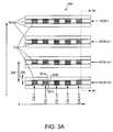
- FIG. 3Adepicts a portion of a memory array including memory elements according to another exemplary embodiment of the invention.
- FIG. 3Billustrates a cross sectional view of a portion of the memory array shown in FIG. 3A taken along line 3 A- 3 A′ and according to an exemplary embodiment of the invention
- FIG. 3Cillustrates a cross sectional view of a portion of the memory array shown in FIG. 3A taken along line 3 A- 3 A′ and according to another exemplary embodiment of the invention
- FIG. 4Adepicts a portion of a memory array including memory elements according to another exemplary embodiment of the invention.
- FIG. 4Billustrates an enlarged portion of the array of FIG. 4A ;
- FIG. 5Adepicts a portion of a memory array including memory elements according to another exemplary embodiment of the invention.
- FIG. 5Billustrates an enlarged portion of the array of FIG. 5A ;
- FIGS. 6A-6Fdepict the formation of the memory elements of FIG. 2A at different stages of processing.
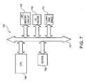
- FIG. 7is a block diagram of a system including a memory element according to an exemplary embodiment of the invention.
- substrateused in the following description may include any supporting structure including, but not limited to, a semiconductor substrate that has an exposed substrate surface.
- a semiconductor substrateshould be understood to include silicon-on-insulator (SOI), silicon-on-sapphire (SOS), doped and undoped semiconductors, epitaxial layers of silicon supported by a base semiconductor foundation, and other semiconductor structures.
- SOIsilicon-on-insulator
- SOSsilicon-on-sapphire
- doped and undoped semiconductorssilicon-on-insulator
- epitaxial layers of silicon supported by a base semiconductor foundationand other semiconductor structures.
- the substrateneed not be semiconductor-based, but may be any support structure suitable for supporting an integrated circuit, including, but not limited to, metals, alloys, glasses, polymers, ceramics, and any other supportive materials as is known in the art.
- resistance variable materialis intended to include materials that can change resistance in response to an applied voltage.
- materialsinclude, as non-limiting examples, chalcogenide glasses, chalcogenide glasses comprising a metal, such as silver, tin, copper, among others; a polymer, such as polymethylphenylacetylene, copperphtalocyanine, polyparaphenylene, polyphenylenevinylene, polyaniline, polythiophene and polypyrrole; and amorphous carbon.
- FIGS. 2A-2Cdepict a portion of a memory array 200 according to exemplary embodiments of the invention.
- FIGS. 2B and 2Care cross-sections illustrating a portion of the memory array 200 of FIG. 2A taken along line 2 A- 2 A′ and according to alternate embodiments of the invention.
- the array 200is supported by a substrate 210 .
- This electrode 212is preferably tungsten (W), but may be any conductive material, such as aluminum, among others.
- An insulating layer 214is between the first electrodes 212 and can be, for example, silicon nitride (Si 3 N 4 ), a low dielectric constant material, an insulating glass, or an insulating polymer, but is not limited to such materials.
- a stack 240 of layersis formed over the first electrodes 212 .
- the stack 240includes one or more layers of resistance variable material.
- the stack 240can include one or more layers of other materials such as, for example, metal.
- the memory cell stack 240includes, for example, a chalcogenide material layer 241 , a tin-chalcogenide layer 242 , and an optional metal layer 243 .
- the stack 240can include additional or fewer layers of other materials suitable for forming a resistance variable memory element.
- the stack 240can include a second chalcogenide material layer (not shown) over the metal layer 243 .
- the second chalcogenide layermay be a same material as the chalcogenide layer 241 or a different material.
- the chalcogenide material layer 241is e.g., germanium selenide (Ge x Se 100 ⁇ x ).
- the germanium selenidemay be within a stoichiometric range of about Ge 33 Se 67 to about Ge 60 Se 40 .
- the chalcogenide material layer 241may be between about 100 ⁇ and about 1000 ⁇ thick, e.g., about 300 ⁇ thick.
- Layer 241need not be a single layer, but may also be comprised of multiple chalcogenide sub-layers having the same or different stoichiometries.
- the chalcogenide material layer 241is in electrical contact with the underlying electrodes 212 .
- chalcogenide material layer 241Over the chalcogenide material layer 241 is an optional layer of metal-chalcogenide 242 , such as tin-chalcogenide (e.g., tin selenide (Sn 1+/ ⁇ x Se, where x is between about 1 and about 0)), or silver-chalcogenide (e.g., silver selenide). It is also possible that other chalcogenide materials may be substituted for selenium, such as sulfur, oxygen, or tellurium.
- the layer 242 in the exemplary embodimentis a layer of tin-chalcogenide layer and may be about 100 ⁇ to about 400 ⁇ thick; however, its thickness depends, in part, on the thickness of the underlying chalcogenide material layer 241 .
- the ratio of the thickness of the tin-chalcogenide layer 242 to that of the underlying chalcogenide material layer 241should be between about 5:1 and about 1:3.
- An optional metal layer 243is provided over the tin-chalcogenide layer 242 , with silver (Ag) being the exemplary metal.
- This metal layer 243is between about 300 ⁇ and about 500 ⁇ thick.
- second (e.g., top) electrodes 251Over the metal layer 243 are second (e.g., top) electrodes 251 .
- the second electrodes 251can be made of the same material as the first electrodes 212 , but are not required to be so formed. In the exemplary embodiment shown in FIGS. 2A and 2B , the second electrodes 251 are preferably tungsten (W).
- stack 240is shown including layers 241 , 242 , 243 , it should be appreciated that one or more of layers 241 , 242 , 243 may be excluded and other layers may be included.
- Non limiting examples of materials and layers that can be included in stack 240 and materials for electrodes 212 , 251are discussed in various patents and patent applications assigned to Micron Technology, Inc., including, but not limited to the following: U.S. patent application Ser. No. 10/765,393; U.S. patent application Ser. No. 09/853,233; U.S. patent application Ser. No. 10/022,722; U.S. patent application Ser. No. 10/663,741; U.S. patent application Ser. No.
- all layers 241 , 242 , 243 of the stack 240are blanket layers extending over the array 200 .
- at least a portion of the stack 240is patterned.
- chalcogenide material layer 241is a blanket layer over the memory array and is shared by all memory elements 201 a , 201 b of the array 200 , and optional metal-chalcogenide layer 242 and optional metal layer 243 are patterned.
- Layers 242 , 243are patterned similarly to the second electrodes 251 , as shown in FIG. 2C .
- Layers 242 , 243 and second electrodes 251are patterned to form longitudinally extending element stacks 202 . While FIG. 2C shows only layers 242 , 243 , 251 as being patterned, it should be appreciated that layer 241 could also be patterned.
- the second electrodes 251are formed as lines along the x (first) direction of a memory array.
- the first electrodes 212have a pitch 208 , which, for example, is the distance in the y direction from about the center of a first electrode 212 b in row n+4 to about the center of a first electrode 212 c in row n+5.
- the second electrodes 251have a pitch 209 , which is approximately the same as the pitch 208 of the first electrodes 212 .
- the second electrodes 251are offset by approximately one half pitch 208 (or 209 ) from the first electrodes 212 . Accordingly, as shown in FIGS.
- each first electrode 212underlies a region 260 between two second electrodes 251 .
- each first electrode 212underlies a portion of two adjacent second electrodes 251 .
- each first electrode 212 of word row nunderlies a portion of the two adjacent second electrodes 251 (one shown above row n in the y (second) direction and a second one below row n in the y direction).
- the array 200includes memory elements 201 a , 201 b , each for storing at least one bit, i.e., a logic 1 or 0. Since each first electrode 212 underlies two second electrodes 251 , each first electrode 212 is associated with two memory elements 201 a , 201 b . Accordingly, the bit density of the array 200 can be increased over prior art arrays that have a single first electrode associated with a single second electrode and thus, a single memory element. During operation, conductive pathways 221 a , 221 b are formed, which causes a detectible resistance change across the memory elements 201 a , 201 b , respectively.
- FIGS. 3A-3Cdepict a portion of a memory array 300 according to additional exemplary embodiments of the invention. Specifically, FIG. 3A shows a portion of a memory array 300 . FIGS. 3B and 3C show a cross-section of the memory array 300 of FIG. 3A taken along the line 3 A- 3 A′. The embodiments of FIGS. 3A-3C are similar to those depicted in FIGS. 2A-2C , except that each first electrode 212 is associated with three second electrodes 351 .
- the second electrodes 351are lines along the x direction.
- the first electrodes 212have a pitch 308 in the y direction.
- the second electrodes lines 351are arranged on a smaller pitch 309 than the first electrodes 212 , such that three or more second electrodes 351 are associated with each first electrode 212 .
- three second electrodes 351can address each first electrode 212 , but the array 300 could be configured such that electrodes 351 have an even smaller pitch as compared to the pitch 308 of the first electrodes, such that more than three second electrodes 351 can address a single first electrode 212 .
- the illustrated array 300includes memory elements 301 a , 301 b , 301 c , each for storing at least one bit, i.e., a logic 1 or 0. Since each first electrode 212 is addressable by three second electrodes 351 , each first electrode 212 is associated with three memory elements 301 a , 301 b , 301 c . Accordingly the bit density of the array 300 can be increased over the embodiment shown in FIGS. 2A-2C .
- all layers 241 , 242 , 243 of the stack 240are blanket layers and are continuously shared by all memory elements 301 a , 301 b , 301 c of the array 300 .
- at least a portion of the stack 240is patterned by etching.
- chalcogenide material layer 241is a blanket layer and is shared by all memory elements 301 a , 301 b , 301 c of the array 300 , and tin-chalcogenide layer 242 and metal layer 243 are patterned.
- the layers 242 , 243are patterned similarly to the second electrodes 351 . While FIG. 3C shows only layers 242 , 243 as being patterned, it should be appreciated that layer 241 could also be patterned.
- FIGS. 4A-4Bdepict a portion of a memory array 400 according to another exemplary embodiment of the invention. Specifically, FIG. 4A shows a portion of a memory array 400 and FIG. 4B is an enlarged view of the portion of FIG. 4A .
- the embodiment shown in FIGS. 4A-4Bis similar to those depicted in FIGS. 2A-3C , except that each first electrode 212 is associated with four second electrodes 451 .
- the first electrodes 212have a pitch 408 x in the x direction and 408 y in the y direction.
- the second electrodes 451are arranged to have approximately the same pitches 408 x , 408 y , but are offset from the first electrodes 212 by about one half pitch. Accordingly, the second electrodes 451 have a pitch 409 x , 409 y . Also, it is preferable that the second electrodes 451 directly overlie at least a portion of the first electrode 212 that they address. Specifically, as shown in FIG. 4B , corners 418 of second electrodes 451 a , 451 b , 451 c , 451 d directly overlie corners of a corresponding first electrode 212 .
- the array 400includes memory elements 401 a , 401 b , 401 c , 401 d each for storing at least one bit, i.e., a logic 1 or 0. Since each first electrode 212 is addressable by four second electrodes 451 , each first electrode 212 is associated with four memory elements 401 a , 401 b , 401 c , 401 d . Accordingly the bit density of the array 400 can be increased over the embodiment shown in FIGS. 2A-3C .
- a cross-sectional view of the array 400 along line 4 A- 4 A′would appear similar to the cross-sectional views shown in FIGS. 2B and 2C .
- Second electrodes 451would appear in a same position as the electrodes 251 shown in FIGS. 2B and 2C .
- cross-sectional views of the array 400are omitted and reference is made to FIGS. 2B and 2C .
- the array 400includes stack 240 having layers 241 , 242 , 241 , as represented in FIGS. 2B and 2C . Additionally, the layers 241 , 242 , 243 can be blanket layers (as represented in FIG. 2B ) or a portion of the stack 240 , e.g., layer 242 , 243 , can be patterned (as represented in FIG. 2C ).
- FIGS. 5A-5Bdepict a portion of a memory array 500 according to additional exemplary embodiments of the invention. Specifically, FIG. 5A shows a portion of a memory array 500 and FIG. 5B is an enlarged view of the portion of FIG. 5 A. The embodiments shown in FIGS. 5A-5B are similar to those depicted in FIGS. 2A-4D , except that each first electrode 212 is associated with nine second electrodes 551 .
- the first electrodes 212have a pitch 508 x in the x direction and 508 y in the y direction.
- the second electrodes 551are arranged on a smaller pitches 509 x in the x direction and 509 y in the y direction such that nine second electrodes 551 can address each first electrode 212 .
- nine second electrodes 551can address each first electrode 212 , but the array 500 could be configured such that electrodes 551 have different pitches as compared to the pitches 508 x , 508 y of the first electrodes 212 , such that greater or fewer than nine second electrodes 551 can address a single first electrode 212 .
- the second electrodes 451directly overlie at least a portion of the first electrode 212 that they address. Specifically, as shown in FIG. 5B , corners and/or edges 518 of second electrodes 551 a , 551 b , 551 c , 551 f , 551 i , 551 h , 551 g , 551 d directly overlie corners of a corresponding first electrode 212 . The whole of second electrode 55 l e directly overlies the first electrode 212 .
- the array 500includes memory elements 540 a , 540 b , 540 c , 501 d , 50 l e , 501 f , 501 g , 501 h , 501 i each for storing one bit, i.e., a logic 1 or 0. Since each first electrode 212 is addressable by nine second electrodes 551 , each first electrode 212 is associated with nine memory elements 540 a , 540 b , 540 c , 501 d , 50 l e , 501 f , 501 g , 501 h , 501 i . Accordingly the bit density of the array 500 is increased over the embodiment shown in FIGS. 2A-4B .
- a cross-sectional view of the array 500 taken along line 5 A- 5 A′would appear similar to the cross-sectional views shown in FIGS. 3B and 3C .
- Second electrodes 551would appear in a same position as the electrodes 351 shown in FIGS. 3B and 3C .
- cross-sectional views of the array 500are omitted and reference is made to FIGS. 3B and 3C .
- the array 500includes stack 240 having layers 241 , 242 , 241 , as represented in FIGS. 3B and 3C . Additionally, the layers 241 , 242 , 243 can be blanket layers (as represented in FIG. 3B ) or a portion of the stack 240 , e.g., layer 242 , 243 , can be patterned (as represented in FIG. 3C ).
- FIGS. 2A-2CThe formation the memory array 200 ( FIGS. 2A-2C ) according to one exemplary embodiment of the invention is now described. No particular order is required for any of the actions described herein, except for those logically requiring the results of prior actions. Accordingly, while the actions below are described as being performed in a general order, the order is exemplary only and can be altered if desired. Although the formation of only a portion of an array 200 is shown, it should be appreciated that the memory array 200 can include additional memory elements 201 a , 201 b , which can be formed concurrently.
- a substrate 210is initially provided.
- the substrate 210can be semiconductor-based or another material useful as a supporting structure.
- An insulating layer 214is formed over the substrate 210 .
- the insulating layer 214can be silicon nitride, a low dielectric constant material, or other insulators known in the art, and may be formed by any known method.
- the insulating layer 214e.g., silicon nitride
- An opening 214 a in the insulating layer 214is made, for instance by photolithographic and etching techniques, exposing a portion of the substrate 210 .
- a first electrode 212is formed within the opening 214 a , by forming a layer of conductive material over the insulating layer 214 and in the opening 214 a .
- a chemical mechanical polishing (CMP) stepis performed to remove the conductive material from over the insulating layer 214 .
- the first electrode 212is formed of tungsten, but may be any conductive material.
- At least one layer of a memory stack 240is formed over the insulating layer 214 and first electrodes 212 , as depicted in FIG. 6B .
- a chalcogenide material layer 241is formed over the first electrodes 212 and insulating layer 214 . Formation of the chalcogenide material layer 241 may be accomplished by any suitable method, for example, by sputtering.
- an etch stop layer 231is formed over the chalcogenide material layer 241 . As shown in FIG. 6C , the etch stop layer is patterned to provide openings 231 a over the layer 241 offset from the first electrodes 212 .
- the etch stop layer 231is chosen to have a high selectivity to the etch chemistry used to etch certain layers of the memory cell stack 240 . Accordingly, the particular etch stop layer may depend on the composition of the memory cell stack 240 .
- an exemplary etch stop layeris transparent carbon, although other materials can be used.
- additional layers of the memory stack 240are formed over the etch stop layer and in opening 231 a .
- an optional metal-chalcogenide layer 242e.g., tin-chalcogenide
- the metal-chalcogenide layer 242can be formed by any suitable method, e.g., physical vapor deposition, chemical vapor deposition, co-evaporation, sputtering, among other techniques.
- An optional metal layer 243is formed over the tin-chalcogenide layer 242 .
- the metal layer 243is preferably silver (Ag), or at contains silver, and is formed to a preferred thickness of about 300 ⁇ to about 500 ⁇ .
- the metal layer 243may be deposited by any technique known in the art.
- a conductive materialis deposited over the metal layer 243 to form a second electrode 251 .
- the conductive material for the second electrode 251may be any material suitable for a conductive electrode.
- the second electrode 251is tungsten.
- a photoresist layer 232(or other mask layer) is deposited over the second electrode 251 layer to define second electrodes 251 .
- the second electrode layer 251is etched.
- second electrode layer 251 and layers 242 , 243are etched to define stacks 202 .
- the mask layer 232is formed to define stacks 202 such that the stacks 202 have a width 282 , which is larger than the width 281 of the opening 231 a . This provides for an alignment margin between the mask layers used to define openings 231 a and the photoresist layer 232 .
- the photoresist layer 232is removed, leaving one of the structures shown in FIG. 2B or 2 C.
- Additional stepsmay be performed to complete the memory array 200 .
- an insulating layer(not shown) may be formed over the second electrodes 251 .
- other processing stepscan be conducted to electrically couple the array 200 to peripheral circuitry (not shown) and to include the array 200 in an integrated circuit or processor system, e.g., processor system 700 described below in connection with FIG. 7 .
- any memory array 300FIGS. 3A-3C ), 400 ( FIGS. 4A-4B ), 500 ( FIGS. 5A-5B ) according to the invention.
- the second electrodes 351 , 451 , 551are patterned to achieve the respective structures described in FIGS. 3A-5B .
- FIG. 7illustrates a processor system 700 which includes a memory circuit 748 , e.g., a memory device, which employs memory array 200 constructed according to the invention.
- the circuit 748could instead employ any of memory arrays 300 ( FIGS. 3A-3C ), 400 ( FIGS. 4A-4B ), or 500 ( FIGS. 5A-5B ).
- the processor system 700which can be, for example, a computer system, generally comprises a central processing unit (CPU) 744 , such as a microprocessor, a digital signal processor, or other programmable digital logic devices, which communicates with an input/output (I/O) device 746 over a bus 752 .
- the memory circuit 448communicates with the CPU 744 over bus 752 typically through a memory controller.
- the processor system 700may include peripheral devices such as a floppy disk drive 754 and a compact disc (CD) ROM drive 756 , which also communicate with CPU 744 over the bus 752 .
- Memory circuit 748is preferably constructed as an integrated circuit, which includes a memory array 200 according to the invention. If desired, the memory circuit 748 may be combined with the processor, for example CPU 744 , in a single integrated circuit.
Landscapes
- Semiconductor Memories (AREA)
Abstract
Description
- The invention relates to the field of random access memory (RAM) devices formed using a resistance variable material.
- Resistance variable memory elements, which include Programmable Conductive Random Access Memory (PCRAM) elements using chalcogenides, have been investigated for suitability as semi-volatile and non-volatile random access memory devices. A typical chalcogenide resistance variable memory element is disclosed in U.S. Pat. No. 6,348,365 to Moore and Gilton.
- In a typical chalcogenide resistance variable memory element, a conductive material, for example, silver, tin and copper, is incorporated into a chalcogenide glass. The resistance of the chalcogenide glass can be programmed to stable higher resistance and lower resistance states. An unprogrammed chalcogenide variable resistance element is normally in a higher resistance state. A write operation programs the element to a lower resistance state by applying a voltage potential across the chalcogenide glass and forming a conductive pathway. The element may then be read by applying a voltage pulse of a lesser magnitude than required to program it; the resistance across the memory device is then sensed as higher or lower to define two logic states.
- The programmed lower resistance state of a chalcogenide variable resistance element can remain intact for an indefinite period, typically ranging from hours to weeks, after the voltage potentials are removed; however, some refreshing may be useful. The element can be returned to its higher resistance state by applying a reverse voltage potential of about the same order of magnitude as used to write the device to the lower resistance state. Again, the higher resistance state is maintained in a semi- or non-volatile manner once the voltage potential is removed. In this way, such an element can function as a semi- or non-volatile variable resistance memory having at least two resistance states, which can define two respective logic states, i.e., at least a bit of data.
- One exemplary chalcogenide resistance variable device uses a germanium selenide (i.e., GexSe100−x) chalcogenide glass as a backbone. The germanium selenide glass has, in the prior art, incorporated silver (Ag) and silver selenide (Ag2+/−xSe) layers in the memory element.
FIG. 1 depicts an example of a conventional chalcogenidevariable resistance element 1. Asemiconductive substrate 10, such as a silicon wafer, supports thememory element 1. Over thesubstrate 10 is aninsulating material 11, such as silicon dioxide. Aconductive material 12, such as tungsten, is formed overinsulating material 11.Conductive material 12 functions as a first electrode for theelement 1. An insulating material,13 such as silicon nitride, is formed overconductive material 12. Aglass material 51, such as Ge3Se7, is formed within via22. - A
metal material 41, such as silver, is formed overglass material 51. An irradiation process and/or thermal process are used to cause diffusion of metal ions into theglass material 51. A second conductive electrode61 is formed overdielectric material 13 andmetal material 41. - The
element 1 is programmed by applying a sufficient voltage across theelectrodes 12,61 to cause the formation of a conductive path between the twoelectrodes 12,61, by virtue of a conductor (i.e., such as silver) that is present in metal ionlaced glass layer 51. In the illustrated example, with the programming voltage applied across theelectrodes 12,61, the conductive pathway forms fromelectrode 12 towards electrode61. - A plurality of resistance variable memory elements can be included in a memory array. In doing so, it is desirable to provide a high density of memory elements.
- Exemplary embodiments of the invention provide a memory array having a plurality of resistance variable memory units and methods for forming the same. Each memory unit includes a first electrode, a resistance variable material over the first electrode, and a first second-electrode over the resistance variable material. The first second-electrode is associated with the first electrode to define a first memory element. Each memory unit further includes a second second-electrode over the resistance variable material. The second-second electrode is associated with the first electrode to define a second memory element.
- The foregoing and other advantages and features of the invention will become more apparent from the detailed description of exemplary embodiments provided below with reference to the accompanying drawings in which:
FIG. 1 illustrates a cross sectional view of a conventional resistance variable memory element;FIG. 2A depicts a portion of a memory array including memory elements according to an exemplary embodiment of the invention;FIG. 2B illustrates a cross sectional view of a portion of the memory array shown inFIG. 2A taken alongline 2A-2A′ and according to an exemplary embodiment of the invention;FIG. 2C illustrates a cross sectional view of a portion of the memory array shown inFIG. 2A taken alongline 2A-2A′ and according to another exemplary embodiment of the invention;FIG. 3A depicts a portion of a memory array including memory elements according to another exemplary embodiment of the invention;FIG. 3B illustrates a cross sectional view of a portion of the memory array shown inFIG. 3A taken alongline 3A-3A′ and according to an exemplary embodiment of the invention;FIG. 3C illustrates a cross sectional view of a portion of the memory array shown inFIG. 3A taken alongline 3A-3A′ and according to another exemplary embodiment of the invention;FIG. 4A depicts a portion of a memory array including memory elements according to another exemplary embodiment of the invention;FIG. 4B illustrates an enlarged portion of the array ofFIG. 4A ;FIG. 5A depicts a portion of a memory array including memory elements according to another exemplary embodiment of the invention;FIG. 5B illustrates an enlarged portion of the array ofFIG. 5A ;FIGS. 6A-6F depict the formation of the memory elements ofFIG. 2A at different stages of processing; andFIG. 7 is a block diagram of a system including a memory element according to an exemplary embodiment of the invention.- In the following detailed description, reference is made to various specific embodiments of the invention. These embodiments are described with sufficient detail to enable those skilled in the art to practice the invention. It is to be understood that other embodiments may be employed, and that various structural, logical and electrical changes may be made without departing from the spirit or scope of the invention.
- The term “substrate” used in the following description may include any supporting structure including, but not limited to, a semiconductor substrate that has an exposed substrate surface. A semiconductor substrate should be understood to include silicon-on-insulator (SOI), silicon-on-sapphire (SOS), doped and undoped semiconductors, epitaxial layers of silicon supported by a base semiconductor foundation, and other semiconductor structures. When reference is made to a semiconductor substrate or wafer in the following description, previous process steps may have been utilized to form regions or junctions in or over the base semiconductor or foundation. The substrate need not be semiconductor-based, but may be any support structure suitable for supporting an integrated circuit, including, but not limited to, metals, alloys, glasses, polymers, ceramics, and any other supportive materials as is known in the art.
- The term “resistance variable material” is intended to include materials that can change resistance in response to an applied voltage. Such materials include, as non-limiting examples, chalcogenide glasses, chalcogenide glasses comprising a metal, such as silver, tin, copper, among others; a polymer, such as polymethylphenylacetylene, copperphtalocyanine, polyparaphenylene, polyphenylenevinylene, polyaniline, polythiophene and polypyrrole; and amorphous carbon.
- The invention is now explained with reference to the figures, which illustrate exemplary embodiments and throughout which like reference numbers indicate like features.
FIGS. 2A-2C depict a portion of amemory array 200 according to exemplary embodiments of the invention.FIGS. 2B and 2C are cross-sections illustrating a portion of thememory array 200 ofFIG. 2A taken alongline 2A-2A′ and according to alternate embodiments of the invention. - Referring to
FIGS. 2A and 2B , thearray 200 is supported by asubstrate 210. Over thesubstrate 210, though not necessarily directly so, is a first (e.g., a bottom)electrode 212 for each memory element101a,101b. Thiselectrode 212 is preferably tungsten (W), but may be any conductive material, such as aluminum, among others. An insulatinglayer 214 is between thefirst electrodes 212 and can be, for example, silicon nitride (Si3N4), a low dielectric constant material, an insulating glass, or an insulating polymer, but is not limited to such materials. - A
stack 240 of layers is formed over thefirst electrodes 212. Thestack 240 includes one or more layers of resistance variable material. Thestack 240 can include one or more layers of other materials such as, for example, metal. - In the exemplary embodiments shown in
FIGS. 2A-2C , thememory cell stack 240 includes, for example, achalcogenide material layer 241, a tin-chalcogenide layer 242, and anoptional metal layer 243. The invention, however, is not limited to such embodiments, and thestack 240 can include additional or fewer layers of other materials suitable for forming a resistance variable memory element. For example, thestack 240 can include a second chalcogenide material layer (not shown) over themetal layer 243. The second chalcogenide layer may be a same material as thechalcogenide layer 241 or a different material. - In the illustrated embodiments, the
chalcogenide material layer 241 is e.g., germanium selenide (GexSe100−x). The germanium selenide may be within a stoichiometric range of about Ge33Se67to about Ge60Se40. Thechalcogenide material layer 241 may be between about 100 Å and about 1000 Å thick, e.g., about 300 Å thick.Layer 241 need not be a single layer, but may also be comprised of multiple chalcogenide sub-layers having the same or different stoichiometries. Thechalcogenide material layer 241 is in electrical contact with theunderlying electrodes 212. - Over the
chalcogenide material layer 241 is an optional layer of metal-chalcogenide 242, such as tin-chalcogenide (e.g., tin selenide (Sn1+/−xSe, where x is between about 1 and about 0)), or silver-chalcogenide (e.g., silver selenide). It is also possible that other chalcogenide materials may be substituted for selenium, such as sulfur, oxygen, or tellurium. Thelayer 242 in the exemplary embodiment is a layer of tin-chalcogenide layer and may be about 100 Å to about 400 Å thick; however, its thickness depends, in part, on the thickness of the underlyingchalcogenide material layer 241. The ratio of the thickness of the tin-chalcogenide layer 242 to that of the underlyingchalcogenide material layer 241 should be between about 5:1 and about 1:3. - An
optional metal layer 243 is provided over the tin-chalcogenide layer 242, with silver (Ag) being the exemplary metal. Thismetal layer 243 is between about 300 Å and about 500 Å thick. Over themetal layer 243 are second (e.g., top)electrodes 251. Thesecond electrodes 251 can be made of the same material as thefirst electrodes 212, but are not required to be so formed. In the exemplary embodiment shown inFIGS. 2A and 2B , thesecond electrodes 251 are preferably tungsten (W). - Although in the illustrated exemplary embodiments of the invention, stack240 is shown including
layers layers stack 240 and materials forelectrodes - In the embodiment of
FIG. 2B , alllayers stack 240 are blanket layers extending over thearray 200. In an alternative embodiment shown inFIG. 2C , at least a portion of thestack 240 is patterned. When one or more top layers of thestack 240 are conductive, it is desirable to pattern those layers similarly to thesecond electrodes 251 to avoid thesecond electrodes 251 being shorted together. Specifically, in the embodiment illustrated inFIG. 2C ,chalcogenide material layer 241 is a blanket layer over the memory array and is shared by allmemory elements array 200, and optional metal-chalcogenide layer 242 andoptional metal layer 243 are patterned.Layers second electrodes 251, as shown inFIG. 2C .Layers second electrodes 251 are patterned to form longitudinally extending element stacks202. WhileFIG. 2C shows only layers242,243,251 as being patterned, it should be appreciated thatlayer 241 could also be patterned. - As shown in
FIG. 2A , thesecond electrodes 251 are formed as lines along the x (first) direction of a memory array. Thefirst electrodes 212 have apitch 208, which, for example, is the distance in the y direction from about the center of afirst electrode 212bin row n+4 to about the center of afirst electrode 212cinrow n+ 5. Thesecond electrodes 251 have apitch 209, which is approximately the same as thepitch 208 of thefirst electrodes 212. Thesecond electrodes 251 are offset by approximately one half pitch208 (or209) from thefirst electrodes 212. Accordingly, as shown inFIGS. 2A-2C , eachfirst electrode 212 underlies aregion 260 between twosecond electrodes 251. In the exemplary embodiment ofFIGS. 2A-2C , eachfirst electrode 212 underlies a portion of two adjacentsecond electrodes 251. For example, eachfirst electrode 212 of word row n underlies a portion of the two adjacent second electrodes251 (one shown above row n in the y (second) direction and a second one below row n in the y direction). - The
array 200 includesmemory elements logic 1 or 0. Since eachfirst electrode 212 underlies twosecond electrodes 251, eachfirst electrode 212 is associated with twomemory elements array 200 can be increased over prior art arrays that have a single first electrode associated with a single second electrode and thus, a single memory element. During operation,conductive pathways memory elements FIGS. 3A-3C depict a portion of amemory array 300 according to additional exemplary embodiments of the invention. Specifically,FIG. 3A shows a portion of amemory array 300.FIGS. 3B and 3C show a cross-section of thememory array 300 ofFIG. 3A taken along theline 3A-3A′. The embodiments ofFIGS. 3A-3C are similar to those depicted inFIGS. 2A-2C , except that eachfirst electrode 212 is associated with threesecond electrodes 351.- As shown in
FIG. 3A , thesecond electrodes 351 are lines along the x direction. Thefirst electrodes 212 have apitch 308 in the y direction. Thesecond electrodes lines 351 are arranged on asmaller pitch 309 than thefirst electrodes 212, such that three or moresecond electrodes 351 are associated with eachfirst electrode 212. In the illustrated embodiment, threesecond electrodes 351 can address eachfirst electrode 212, but thearray 300 could be configured such thatelectrodes 351 have an even smaller pitch as compared to thepitch 308 of the first electrodes, such that more than threesecond electrodes 351 can address a singlefirst electrode 212. - The illustrated
array 300 includesmemory elements logic 1 or 0. Since eachfirst electrode 212 is addressable by threesecond electrodes 351, eachfirst electrode 212 is associated with threememory elements array 300 can be increased over the embodiment shown inFIGS. 2A-2C . - In the embodiment shown in
FIG. 3B alllayers stack 240 are blanket layers and are continuously shared by allmemory elements array 300. In an alternative embodiment shown inFIG. 3C , at least a portion of thestack 240 is patterned by etching. Specifically, in the embodiment illustrated inFIG. 3C ,chalcogenide material layer 241 is a blanket layer and is shared by allmemory elements array 300, and tin-chalcogenide layer 242 andmetal layer 243 are patterned. Thelayers second electrodes 351. WhileFIG. 3C shows only layers242,243 as being patterned, it should be appreciated thatlayer 241 could also be patterned. FIGS. 4A-4B depict a portion of amemory array 400 according to another exemplary embodiment of the invention. Specifically,FIG. 4A shows a portion of amemory array 400 andFIG. 4B is an enlarged view of the portion ofFIG. 4A . The embodiment shown inFIGS. 4A-4B is similar to those depicted inFIGS. 2A-3C , except that eachfirst electrode 212 is associated with foursecond electrodes 451.- As shown in
FIG. 4A , thefirst electrodes 212 have apitch 408xin the x direction and408yin the y direction. Thesecond electrodes 451 are arranged to have approximately thesame pitches first electrodes 212 by about one half pitch. Accordingly, thesecond electrodes 451 have apitch second electrodes 451 directly overlie at least a portion of thefirst electrode 212 that they address. Specifically, as shown inFIG. 4B ,corners 418 ofsecond electrodes first electrode 212. - The
array 400 includesmemory elements logic 1 or 0. Since eachfirst electrode 212 is addressable by foursecond electrodes 451, eachfirst electrode 212 is associated with fourmemory elements array 400 can be increased over the embodiment shown inFIGS. 2A-3C . - A cross-sectional view of the
array 400 alongline 4A-4A′ would appear similar to the cross-sectional views shown inFIGS. 2B and 2C .Second electrodes 451 would appear in a same position as theelectrodes 251 shown inFIGS. 2B and 2C . For simplicity, cross-sectional views of thearray 400 are omitted and reference is made toFIGS. 2B and 2C . Thearray 400 includesstack 240 havinglayers FIGS. 2B and 2C . Additionally, thelayers FIG. 2B ) or a portion of thestack 240, e.g.,layer FIG. 2C ). FIGS. 5A-5B depict a portion of amemory array 500 according to additional exemplary embodiments of the invention. Specifically,FIG. 5A shows a portion of amemory array 500 andFIG. 5B is an enlarged view of the portion of FIG.5A. The embodiments shown inFIGS. 5A-5B are similar to those depicted inFIGS. 2A-4D , except that eachfirst electrode 212 is associated with ninesecond electrodes 551.- As shown in
FIG. 5A , thefirst electrodes 212 have apitch 508xin the x direction and508yin the y direction. Thesecond electrodes 551 are arranged on asmaller pitches 509xin the x direction and509yin the y direction such that ninesecond electrodes 551 can address eachfirst electrode 212. In the illustrated embodiment, ninesecond electrodes 551 can address eachfirst electrode 212, but thearray 500 could be configured such thatelectrodes 551 have different pitches as compared to thepitches first electrodes 212, such that greater or fewer than ninesecond electrodes 551 can address a singlefirst electrode 212. - Also, it is preferable that the
second electrodes 451 directly overlie at least a portion of thefirst electrode 212 that they address. Specifically, as shown inFIG. 5B , corners and/oredges 518 ofsecond electrodes first electrode 212. The whole of second electrode55ledirectly overlies thefirst electrode 212. - The
array 500 includesmemory elements 540a,540b,540c,501d,50le,501f,501g,501h,501ieach for storing one bit, i.e., alogic 1 or 0. Since eachfirst electrode 212 is addressable by ninesecond electrodes 551, eachfirst electrode 212 is associated with ninememory elements 540a,540b,540c,501d,50le,501f,501g,501h,501i. Accordingly the bit density of thearray 500 is increased over the embodiment shown inFIGS. 2A-4B . - A cross-sectional view of the
array 500 taken alongline 5A-5A′ would appear similar to the cross-sectional views shown inFIGS. 3B and 3C .Second electrodes 551 would appear in a same position as theelectrodes 351 shown inFIGS. 3B and 3C . For simplicity, cross-sectional views of thearray 500 are omitted and reference is made toFIGS. 3B and 3C . Thearray 500 includesstack 240 havinglayers FIGS. 3B and 3C . Additionally, thelayers FIG. 3B ) or a portion of thestack 240, e.g.,layer FIG. 3C ). - The formation the memory array200 (
FIGS. 2A-2C ) according to one exemplary embodiment of the invention is now described. No particular order is required for any of the actions described herein, except for those logically requiring the results of prior actions. Accordingly, while the actions below are described as being performed in a general order, the order is exemplary only and can be altered if desired. Although the formation of only a portion of anarray 200 is shown, it should be appreciated that thememory array 200 can includeadditional memory elements - As shown by
FIG. 6A , asubstrate 210 is initially provided. As indicated above, thesubstrate 210 can be semiconductor-based or another material useful as a supporting structure. An insulatinglayer 214 is formed over thesubstrate 210. The insulatinglayer 214 can be silicon nitride, a low dielectric constant material, or other insulators known in the art, and may be formed by any known method. Preferably, the insulating layer214 (e.g., silicon nitride) does not allow metal ion migration from the optional metal-chalcogenide layer 242. Anopening 214ain the insulatinglayer 214 is made, for instance by photolithographic and etching techniques, exposing a portion of thesubstrate 210. Afirst electrode 212 is formed within the opening214a, by forming a layer of conductive material over the insulatinglayer 214 and in theopening 214a. A chemical mechanical polishing (CMP) step is performed to remove the conductive material from over the insulatinglayer 214. Desirably, thefirst electrode 212 is formed of tungsten, but may be any conductive material. - At least one layer of a
memory stack 240 is formed over the insulatinglayer 214 andfirst electrodes 212, as depicted inFIG. 6B . In the illustrated embodiment, achalcogenide material layer 241 is formed over thefirst electrodes 212 and insulatinglayer 214. Formation of thechalcogenide material layer 241 may be accomplished by any suitable method, for example, by sputtering. - When it is desirable to etch one or more layers of the stack240 (
FIG. 2C ), anetch stop layer 231 is formed over thechalcogenide material layer 241. As shown inFIG. 6C , the etch stop layer is patterned to provideopenings 231aover thelayer 241 offset from thefirst electrodes 212. Theetch stop layer 231 is chosen to have a high selectivity to the etch chemistry used to etch certain layers of thememory cell stack 240. Accordingly, the particular etch stop layer may depend on the composition of thememory cell stack 240. In the illustrated embodiment, an exemplary etch stop layer is transparent carbon, although other materials can be used. - As shown in
FIG. 6D , additional layers of thememory stack 240 are formed over the etch stop layer and in opening231a. In the illustrated embodiment, an optional metal-chalcogenide layer242 (e.g., tin-chalcogenide) is formed over the etch stop layer and in opening231aand in contact with thechalcogenide material layer 241. The metal-chalcogenide layer 242 can be formed by any suitable method, e.g., physical vapor deposition, chemical vapor deposition, co-evaporation, sputtering, among other techniques. Anoptional metal layer 243 is formed over the tin-chalcogenide layer 242. Themetal layer 243 is preferably silver (Ag), or at contains silver, and is formed to a preferred thickness of about 300 Å to about 500 Å. Themetal layer 243 may be deposited by any technique known in the art. - When the structure of
FIG. 2B is desired, formation of theetch stop layer 231 is omitted and thelayer layer 241. - Referring to
FIG. 6E , a conductive material is deposited over themetal layer 243 to form asecond electrode 251. Similar to thefirst electrode 212, the conductive material for thesecond electrode 251 may be any material suitable for a conductive electrode. In one exemplary embodiment thesecond electrode 251 is tungsten. - As illustrated in
FIG. 6F , a photoresist layer232 (or other mask layer) is deposited over thesecond electrode 251 layer to definesecond electrodes 251. When the structure ofFIG. 2B is desired, only thesecond electrode layer 251 is etched. When the structure ofFIG. 2B is desired,second electrode layer 251 andlayers stacks 202. The etching stops at theetch stop layer 231. Desirably, themask layer 232 is formed to definestacks 202 such that thestacks 202 have awidth 282, which is larger than thewidth 281 of the opening231a. This provides for an alignment margin between the mask layers used to defineopenings 231aand thephotoresist layer 232. - The
photoresist layer 232 is removed, leaving one of the structures shown inFIG. 2B or2C. - Additional steps may be performed to complete the
memory array 200. For example, an insulating layer (not shown) may be formed over thesecond electrodes 251. Also, other processing steps can be conducted to electrically couple thearray 200 to peripheral circuitry (not shown) and to include thearray 200 in an integrated circuit or processor system, e.g.,processor system 700 described below in connection withFIG. 7 . - The method described above can be used to form any memory array300 (
FIGS. 3A-3C ),400 (FIGS. 4A-4B ),500 (FIGS. 5A-5B ) according to the invention. When forming any of thearrays second electrodes FIGS. 3A-5B . FIG. 7 illustrates aprocessor system 700 which includes amemory circuit 748, e.g., a memory device, which employsmemory array 200 constructed according to the invention. Thecircuit 748 could instead employ any of memory arrays300 (FIGS. 3A-3C ),400 (FIGS. 4A-4B ), or500 (FIGS. 5A-5B ). Theprocessor system 700, which can be, for example, a computer system, generally comprises a central processing unit (CPU)744, such as a microprocessor, a digital signal processor, or other programmable digital logic devices, which communicates with an input/output (I/O)device 746 over abus 752. The memory circuit448 communicates with theCPU 744 overbus 752 typically through a memory controller.- In the case of a computer system, the
processor system 700 may include peripheral devices such as afloppy disk drive 754 and a compact disc (CD)ROM drive 756, which also communicate withCPU 744 over thebus 752.Memory circuit 748 is preferably constructed as an integrated circuit, which includes amemory array 200 according to the invention. If desired, thememory circuit 748 may be combined with the processor, forexample CPU 744, in a single integrated circuit. - The above description and drawings are only to be considered illustrative of exemplary embodiments, which achieve the features and advantages of the present invention. Modification and substitutions to specific process conditions and structures can be made without departing from the spirit and scope of the present invention. Accordingly, the invention is not to be considered as being limited by the foregoing description and drawings, but is only limited by the scope of the appended claims.
Claims (52)
Priority Applications (3)
| Application Number | Priority Date | Filing Date | Title |
|---|---|---|---|
| US11/111,836US7427770B2 (en) | 2005-04-22 | 2005-04-22 | Memory array for increased bit density |
| US11/585,795US7700422B2 (en) | 2005-04-22 | 2006-10-25 | Methods of forming memory arrays for increased bit density |
| US12/659,612US7968927B2 (en) | 2005-04-22 | 2010-03-15 | Memory array for increased bit density and method of forming the same |
Applications Claiming Priority (1)
| Application Number | Priority Date | Filing Date | Title |
|---|---|---|---|
| US11/111,836US7427770B2 (en) | 2005-04-22 | 2005-04-22 | Memory array for increased bit density |
Related Child Applications (1)
| Application Number | Title | Priority Date | Filing Date |
|---|---|---|---|
| US11/585,795DivisionUS7700422B2 (en) | 2005-04-22 | 2006-10-25 | Methods of forming memory arrays for increased bit density |
Publications (2)
| Publication Number | Publication Date |
|---|---|
| US20060237707A1true US20060237707A1 (en) | 2006-10-26 |
| US7427770B2 US7427770B2 (en) | 2008-09-23 |
Family
ID=37185926
Family Applications (3)
| Application Number | Title | Priority Date | Filing Date |
|---|---|---|---|
| US11/111,836Expired - LifetimeUS7427770B2 (en) | 2005-04-22 | 2005-04-22 | Memory array for increased bit density |
| US11/585,795Expired - LifetimeUS7700422B2 (en) | 2005-04-22 | 2006-10-25 | Methods of forming memory arrays for increased bit density |
| US12/659,612Expired - LifetimeUS7968927B2 (en) | 2005-04-22 | 2010-03-15 | Memory array for increased bit density and method of forming the same |
Family Applications After (2)
| Application Number | Title | Priority Date | Filing Date |
|---|---|---|---|
| US11/585,795Expired - LifetimeUS7700422B2 (en) | 2005-04-22 | 2006-10-25 | Methods of forming memory arrays for increased bit density |
| US12/659,612Expired - LifetimeUS7968927B2 (en) | 2005-04-22 | 2010-03-15 | Memory array for increased bit density and method of forming the same |
Country Status (1)
| Country | Link |
|---|---|
| US (3) | US7427770B2 (en) |
Families Citing this family (4)
| Publication number | Priority date | Publication date | Assignee | Title |
|---|---|---|---|---|
| US7427770B2 (en) | 2005-04-22 | 2008-09-23 | Micron Technology, Inc. | Memory array for increased bit density |
| US7709289B2 (en)* | 2005-04-22 | 2010-05-04 | Micron Technology, Inc. | Memory elements having patterned electrodes and method of forming the same |
| US7964869B2 (en)* | 2006-08-25 | 2011-06-21 | Panasonic Corporation | Memory element, memory apparatus, and semiconductor integrated circuit |
| US7560723B2 (en) | 2006-08-29 | 2009-07-14 | Micron Technology, Inc. | Enhanced memory density resistance variable memory cells, arrays, devices and systems including the same, and methods of fabrication |
Citations (92)
| Publication number | Priority date | Publication date | Assignee | Title |
|---|---|---|---|---|
| US3961314A (en)* | 1974-03-05 | 1976-06-01 | Energy Conversion Devices, Inc. | Structure and method for producing an image |
| US3966317A (en)* | 1974-04-08 | 1976-06-29 | Energy Conversion Devices, Inc. | Dry process production of archival microform records from hard copy |
| US4267261A (en)* | 1971-07-15 | 1981-05-12 | Energy Conversion Devices, Inc. | Method for full format imaging |
| US4269935A (en)* | 1979-07-13 | 1981-05-26 | Ionomet Company, Inc. | Process of doping silver image in chalcogenide layer |
| US4312938A (en)* | 1979-07-06 | 1982-01-26 | Drexler Technology Corporation | Method for making a broadband reflective laser recording and data storage medium with absorptive underlayer |
| US4316946A (en)* | 1979-12-03 | 1982-02-23 | Ionomet Company, Inc. | Surface sensitized chalcogenide product and process for making and using the same |
| US4320191A (en)* | 1978-11-07 | 1982-03-16 | Nippon Telegraph & Telephone Public Corporation | Pattern-forming process |
| US4499557A (en)* | 1980-10-28 | 1985-02-12 | Energy Conversion Devices, Inc. | Programmable cell for use in programmable electronic arrays |
| US4637895A (en)* | 1985-04-01 | 1987-01-20 | Energy Conversion Devices, Inc. | Gas mixtures for the vapor deposition of semiconductor material |
| US4646266A (en)* | 1984-09-28 | 1987-02-24 | Energy Conversion Devices, Inc. | Programmable semiconductor structures and methods for using the same |
| US4664939A (en)* | 1985-04-01 | 1987-05-12 | Energy Conversion Devices, Inc. | Vertical semiconductor processor |
| US4668968A (en)* | 1984-05-14 | 1987-05-26 | Energy Conversion Devices, Inc. | Integrated circuit compatible thin film field effect transistor and method of making same |
| US4670763A (en)* | 1984-05-14 | 1987-06-02 | Energy Conversion Devices, Inc. | Thin film field effect transistor |
| US4671618A (en)* | 1986-05-22 | 1987-06-09 | Wu Bao Gang | Liquid crystalline-plastic material having submillisecond switch times and extended memory |
| US4673957A (en)* | 1984-05-14 | 1987-06-16 | Energy Conversion Devices, Inc. | Integrated circuit compatible thin film field effect transistor and method of making same |
| US4728406A (en)* | 1986-08-18 | 1988-03-01 | Energy Conversion Devices, Inc. | Method for plasma - coating a semiconductor body |
| US4737379A (en)* | 1982-09-24 | 1988-04-12 | Energy Conversion Devices, Inc. | Plasma deposited coatings, and low temperature plasma method of making same |
| US4795657A (en)* | 1984-04-13 | 1989-01-03 | Energy Conversion Devices, Inc. | Method of fabricating a programmable array |
| US4800526A (en)* | 1987-05-08 | 1989-01-24 | Gaf Corporation | Memory element for information storage and retrieval system and associated process |
| US4809044A (en)* | 1986-08-22 | 1989-02-28 | Energy Conversion Devices, Inc. | Thin film overvoltage protection devices |
| US4818717A (en)* | 1986-06-27 | 1989-04-04 | Energy Conversion Devices, Inc. | Method for making electronic matrix arrays |
| US4843443A (en)* | 1984-05-14 | 1989-06-27 | Energy Conversion Devices, Inc. | Thin film field effect transistor and method of making same |
| US4891330A (en)* | 1987-07-27 | 1990-01-02 | Energy Conversion Devices, Inc. | Method of fabricating n-type and p-type microcrystalline semiconductor alloy material including band gap widening elements |
| US5177567A (en)* | 1991-07-19 | 1993-01-05 | Energy Conversion Devices, Inc. | Thin-film structure for chalcogenide electrical switching devices and process therefor |
| US5219788A (en)* | 1991-02-25 | 1993-06-15 | Ibm Corporation | Bilayer metallization cap for photolithography |
| US5296716A (en)* | 1991-01-18 | 1994-03-22 | Energy Conversion Devices, Inc. | Electrically erasable, directly overwritable, multibit single cell memory elements and arrays fabricated therefrom |
| US5314772A (en)* | 1990-10-09 | 1994-05-24 | Arizona Board Of Regents | High resolution, multi-layer resist for microlithography and method therefor |
| US5315131A (en)* | 1990-11-22 | 1994-05-24 | Matsushita Electric Industrial Co., Ltd. | Electrically reprogrammable nonvolatile memory device |
| US5406509A (en)* | 1991-01-18 | 1995-04-11 | Energy Conversion Devices, Inc. | Electrically erasable, directly overwritable, multibit single cell memory elements and arrays fabricated therefrom |
| US5414271A (en)* | 1991-01-18 | 1995-05-09 | Energy Conversion Devices, Inc. | Electrically erasable memory elements having improved set resistance stability |
| US5500532A (en)* | 1994-08-18 | 1996-03-19 | Arizona Board Of Regents | Personal electronic dosimeter |
| US5512773A (en)* | 1993-12-23 | 1996-04-30 | U.S. Philips Corporation | Switching element with memory provided with Schottky tunnelling barrier |
| US5512328A (en)* | 1992-08-07 | 1996-04-30 | Hitachi, Ltd. | Method for forming a pattern and forming a thin film used in pattern formation |
| US5591501A (en)* | 1995-12-20 | 1997-01-07 | Energy Conversion Devices, Inc. | Optical recording medium having a plurality of discrete phase change data recording points |
| US5596522A (en)* | 1991-01-18 | 1997-01-21 | Energy Conversion Devices, Inc. | Homogeneous compositions of microcrystalline semiconductor material, semiconductor devices and directly overwritable memory elements fabricated therefrom, and arrays fabricated from the memory elements |
| US5714768A (en)* | 1995-10-24 | 1998-02-03 | Energy Conversion Devices, Inc. | Second-layer phase change memory array on top of a logic device |
| US5726083A (en)* | 1994-11-29 | 1998-03-10 | Nec Corporation | Process of fabricating dynamic random access memory device having storage capacitor low in contact resistance and small in leakage current through tantalum oxide film |
| US5751012A (en)* | 1995-06-07 | 1998-05-12 | Micron Technology, Inc. | Polysilicon pillar diode for use in a non-volatile memory cell |
| US5761115A (en)* | 1996-05-30 | 1998-06-02 | Axon Technologies Corporation | Programmable metallization cell structure and method of making same |
| US5869843A (en)* | 1995-06-07 | 1999-02-09 | Micron Technology, Inc. | Memory array having a multi-state element and method for forming such array or cells thereof |
| US5912839A (en)* | 1998-06-23 | 1999-06-15 | Energy Conversion Devices, Inc. | Universal memory element and method of programming same |
| US6011757A (en)* | 1998-01-27 | 2000-01-04 | Ovshinsky; Stanford R. | Optical recording media having increased erasability |
| US6031287A (en)* | 1997-06-18 | 2000-02-29 | Micron Technology, Inc. | Contact structure and memory element incorporating the same |
| US6072716A (en)* | 1999-04-14 | 2000-06-06 | Massachusetts Institute Of Technology | Memory structures and methods of making same |
| US6177338B1 (en)* | 1999-02-08 | 2001-01-23 | Taiwan Semiconductor Manufacturing Company | Two step barrier process |
| US6236059B1 (en)* | 1996-08-22 | 2001-05-22 | Micron Technology, Inc. | Memory cell incorporating a chalcogenide element and method of making same |
| US20020000666A1 (en)* | 1998-08-31 | 2002-01-03 | Michael N. Kozicki | Self-repairing interconnections for electrical circuits |
| US6339544B1 (en)* | 2000-09-29 | 2002-01-15 | Intel Corporation | Method to enhance performance of thermal resistor device |
| US6348365B1 (en)* | 2001-03-02 | 2002-02-19 | Micron Technology, Inc. | PCRAM cell manufacturing |
| US6350679B1 (en)* | 1999-08-03 | 2002-02-26 | Micron Technology, Inc. | Methods of providing an interlevel dielectric layer intermediate different elevation conductive metal layers in the fabrication of integrated circuitry |
| US6376284B1 (en)* | 1996-02-23 | 2002-04-23 | Micron Technology, Inc. | Method of fabricating a memory device |
| US6391688B1 (en)* | 1995-06-07 | 2002-05-21 | Micron Technology, Inc. | Method for fabricating an array of ultra-small pores for chalcogenide memory cells |
| US20030001229A1 (en)* | 2001-03-01 | 2003-01-02 | Moore John T. | Chalcogenide comprising device |
| US20030001230A1 (en)* | 2000-06-30 | 2003-01-02 | Lowrey Tyler A. | Three dimensional programmable device and method for fabricating the same |
| US6507061B1 (en)* | 2001-08-31 | 2003-01-14 | Intel Corporation | Multiple layer phase-change memory |
| US6511862B2 (en)* | 2001-06-30 | 2003-01-28 | Ovonyx, Inc. | Modified contact for programmable devices |
| US6511867B2 (en)* | 2001-06-30 | 2003-01-28 | Ovonyx, Inc. | Utilizing atomic layer deposition for programmable device |
| US6512241B1 (en)* | 2001-12-31 | 2003-01-28 | Intel Corporation | Phase change material memory device |
| US6514805B2 (en)* | 2001-06-30 | 2003-02-04 | Intel Corporation | Trench sidewall profile for device isolation |
| US20030027416A1 (en)* | 2001-08-01 | 2003-02-06 | Moore John T. | Method of forming integrated circuitry, method of forming memory circuitry, and method of forming random access memory circuitry |
| US20030032254A1 (en)* | 2000-12-08 | 2003-02-13 | Gilton Terry L. | Resistance variable device, analog memory device, and programmable memory cell |
| US20030035314A1 (en)* | 1998-12-04 | 2003-02-20 | Kozicki Michael N. | Programmable microelectronic devices and methods of forming and programming same |
| US20030035315A1 (en)* | 2001-04-06 | 2003-02-20 | Kozicki Michael N. | Microelectronic device, structure, and system, including a memory structure having a variable programmable property and method of forming the same |
| US20030038301A1 (en)* | 2001-08-27 | 2003-02-27 | John Moore | Apparatus and method for dual cell common electrode PCRAM memory device |
| US20030045054A1 (en)* | 2001-08-29 | 2003-03-06 | Campbell Kristy A. | Method of forming non-volatile resistance variable devices, method of forming a programmable memory cell of memory circuitry, and a non-volatile resistance variable device |
| US20030043631A1 (en)* | 2001-08-30 | 2003-03-06 | Gilton Terry L. | Method of retaining memory state in a programmable conductor RAM |
| US20030045049A1 (en)* | 2001-08-29 | 2003-03-06 | Campbell Kristy A. | Method of forming chalcogenide comprising devices |
| US6531373B2 (en)* | 2000-12-27 | 2003-03-11 | Ovonyx, Inc. | Method of forming a phase-change memory cell using silicon on insulator low electrode in charcogenide elements |
| US20030047773A1 (en)* | 2001-03-15 | 2003-03-13 | Jiutao Li | Agglomeration elimination for metal sputter deposition of chalcogenides |
| US20030049912A1 (en)* | 2001-08-29 | 2003-03-13 | Campbell Kristy A. | Method of forming chalcogenide comprsing devices and method of forming a programmable memory cell of memory circuitry |
| US20030048744A1 (en)* | 2001-09-01 | 2003-03-13 | Ovshinsky Stanford R. | Increased data storage in optical data storage and retrieval systems using blue lasers and/or plasmon lenses |
| US20030047765A1 (en)* | 2001-08-30 | 2003-03-13 | Campbell Kristy A. | Stoichiometry for chalcogenide glasses useful for memory devices and method of formation |
| US6534781B2 (en)* | 2000-12-26 | 2003-03-18 | Ovonyx, Inc. | Phase-change memory bipolar array utilizing a single shallow trench isolation for creating an individual active area region for two memory array elements and one bipolar base contact |
| US6545287B2 (en)* | 2001-09-07 | 2003-04-08 | Intel Corporation | Using selective deposition to form phase-change memory cells |
| US6545907B1 (en)* | 2001-10-30 | 2003-04-08 | Ovonyx, Inc. | Technique and apparatus for performing write operations to a phase change material memory device |
| US20030068861A1 (en)* | 2001-08-30 | 2003-04-10 | Jiutao Li | Integrated circuit device and fabrication using metal-doped chalcogenide materials |
| US6555860B2 (en)* | 2000-09-29 | 2003-04-29 | Intel Corporation | Compositionally modified resistive electrode |
| US6563164B2 (en)* | 2000-09-29 | 2003-05-13 | Ovonyx, Inc. | Compositionally modified resistive electrode |
| US6566700B2 (en)* | 2001-10-11 | 2003-05-20 | Ovonyx, Inc. | Carbon-containing interfacial layer for phase-change memory |
| US6567293B1 (en)* | 2000-09-29 | 2003-05-20 | Ovonyx, Inc. | Single level metal memory cell using chalcogenide cladding |
| US20030096497A1 (en)* | 2001-11-19 | 2003-05-22 | Micron Technology, Inc. | Electrode structure for use in an integrated circuit |
| US20030095426A1 (en)* | 2001-11-20 | 2003-05-22 | Glen Hush | Complementary bit PCRAM sense amplifier and method of operation |
| US6569705B2 (en)* | 2000-12-21 | 2003-05-27 | Intel Corporation | Metal structure for a phase-change memory device |
| US6570784B2 (en)* | 2001-06-29 | 2003-05-27 | Ovonyx, Inc. | Programming a phase-change material memory |
| US6673700B2 (en)* | 2001-06-30 | 2004-01-06 | Ovonyx, Inc. | Reduced area intersection between electrode and programming element |
| US6673648B2 (en)* | 2001-11-08 | 2004-01-06 | Intel Corporation | Isolating phase change material memory cells |
| US6687427B2 (en)* | 2000-12-29 | 2004-02-03 | Intel Corporation | Optic switch |
| US6690026B2 (en)* | 2001-09-28 | 2004-02-10 | Intel Corporation | Method of fabricating a three-dimensional array of active media |
| US6696355B2 (en)* | 2000-12-14 | 2004-02-24 | Ovonyx, Inc. | Method to selectively increase the top resistance of the lower programming electrode in a phase-change memory |
| US20040035401A1 (en)* | 2002-08-26 | 2004-02-26 | Subramanian Ramachandran | Hydrogen powered scooter |
| US6707712B2 (en)* | 2001-08-02 | 2004-03-16 | Intel Corporation | Method for reading a structural phase-change memory |
| US6714954B2 (en)* | 2002-05-10 | 2004-03-30 | Energy Conversion Devices, Inc. | Methods of factoring and modular arithmetic |
Family Cites Families (120)
| Publication number | Priority date | Publication date | Assignee | Title |
|---|---|---|---|---|
| US3271591A (en) | 1963-09-20 | 1966-09-06 | Energy Conversion Devices Inc | Symmetrical current controlling device |
| US3622319A (en) | 1966-10-20 | 1971-11-23 | Western Electric Co | Nonreflecting photomasks and methods of making same |
| US3868651A (en) | 1970-08-13 | 1975-02-25 | Energy Conversion Devices Inc | Method and apparatus for storing and reading data in a memory having catalytic material to initiate amorphous to crystalline change in memory structure |
| US3743847A (en) | 1971-06-01 | 1973-07-03 | Motorola Inc | Amorphous silicon film as a uv filter |
| US4177474A (en) | 1977-05-18 | 1979-12-04 | Energy Conversion Devices, Inc. | High temperature amorphous semiconductor member and method of making the same |
| DE2901303C2 (en) | 1979-01-15 | 1984-04-19 | Max Planck Gesellschaft Zur Foerderung Der Wissenschaften E.V., 3400 Goettingen | Solid ionic conductor material, its use and process for its manufacture |
| US4405710A (en) | 1981-06-22 | 1983-09-20 | Cornell Research Foundation, Inc. | Ion beam exposure of (g-Gex -Se1-x) inorganic resists |
| US4545111A (en) | 1983-01-18 | 1985-10-08 | Energy Conversion Devices, Inc. | Method for making, parallel preprogramming or field programming of electronic matrix arrays |
| US4608296A (en) | 1983-12-06 | 1986-08-26 | Energy Conversion Devices, Inc. | Superconducting films and devices exhibiting AC to DC conversion |
| US4769338A (en) | 1984-05-14 | 1988-09-06 | Energy Conversion Devices, Inc. | Thin film field effect transistor and method of making same |
| US4678679A (en) | 1984-06-25 | 1987-07-07 | Energy Conversion Devices, Inc. | Continuous deposition of activated process gases |
| US4710899A (en) | 1985-06-10 | 1987-12-01 | Energy Conversion Devices, Inc. | Data storage medium incorporating a transition metal for increased switching speed |
| US4766471A (en) | 1986-01-23 | 1988-08-23 | Energy Conversion Devices, Inc. | Thin film electro-optical devices |
| US4845533A (en) | 1986-08-22 | 1989-07-04 | Energy Conversion Devices, Inc. | Thin film electrical devices with amorphous carbon electrodes and method of making same |
| US4853785A (en) | 1986-10-15 | 1989-08-01 | Energy Conversion Devices, Inc. | Electronic camera including electronic signal storage cartridge |
| US4788594A (en) | 1986-10-15 | 1988-11-29 | Energy Conversion Devices, Inc. | Solid state electronic camera including thin film matrix of photosensors |
| US4847674A (en) | 1987-03-10 | 1989-07-11 | Advanced Micro Devices, Inc. | High speed interconnect system with refractory non-dogbone contacts and an active electromigration suppression mechanism |
| US4775425A (en) | 1987-07-27 | 1988-10-04 | Energy Conversion Devices, Inc. | P and n-type microcrystalline semiconductor alloy material including band gap widening elements, devices utilizing same |
| US5272359A (en) | 1988-04-07 | 1993-12-21 | California Institute Of Technology | Reversible non-volatile switch based on a TCNQ charge transfer complex |
| GB8910854D0 (en) | 1989-05-11 | 1989-06-28 | British Petroleum Co Plc | Semiconductor device |
| US5159661A (en) | 1990-10-05 | 1992-10-27 | Energy Conversion Devices, Inc. | Vertically interconnected parallel distributed processor |
| US5534711A (en) | 1991-01-18 | 1996-07-09 | Energy Conversion Devices, Inc. | Electrically erasable, directly overwritable, multibit single cell memory elements and arrays fabricated therefrom |
| US5335219A (en) | 1991-01-18 | 1994-08-02 | Ovshinsky Stanford R | Homogeneous composition of microcrystalline semiconductor material, semiconductor devices and directly overwritable memory elements fabricated therefrom, and arrays fabricated from the memory elements |
| US5534712A (en) | 1991-01-18 | 1996-07-09 | Energy Conversion Devices, Inc. | Electrically erasable memory elements characterized by reduced current and improved thermal stability |
| US5166758A (en) | 1991-01-18 | 1992-11-24 | Energy Conversion Devices, Inc. | Electrically erasable phase change memory |
| US5341328A (en) | 1991-01-18 | 1994-08-23 | Energy Conversion Devices, Inc. | Electrically erasable memory elements having reduced switching current requirements and increased write/erase cycle life |
| US5536947A (en) | 1991-01-18 | 1996-07-16 | Energy Conversion Devices, Inc. | Electrically erasable, directly overwritable, multibit single cell memory element and arrays fabricated therefrom |
| US5128099A (en) | 1991-02-15 | 1992-07-07 | Energy Conversion Devices, Inc. | Congruent state changeable optical memory material and device |
| US5359205A (en) | 1991-11-07 | 1994-10-25 | Energy Conversion Devices, Inc. | Electrically erasable memory elements characterized by reduced current and improved thermal stability |
| US5238862A (en) | 1992-03-18 | 1993-08-24 | Micron Technology, Inc. | Method of forming a stacked capacitor with striated electrode |
| US5350484A (en) | 1992-09-08 | 1994-09-27 | Intel Corporation | Method for the anisotropic etching of metal films in the fabrication of interconnects |
| US5818749A (en) | 1993-08-20 | 1998-10-06 | Micron Technology, Inc. | Integrated circuit memory device |
| US5543737A (en) | 1995-02-10 | 1996-08-06 | Energy Conversion Devices, Inc. | Logical operation circuit employing two-terminal chalcogenide switches |
| US6420725B1 (en) | 1995-06-07 | 2002-07-16 | Micron Technology, Inc. | Method and apparatus for forming an integrated circuit electrode having a reduced contact area |
| US5789758A (en) | 1995-06-07 | 1998-08-04 | Micron Technology, Inc. | Chalcogenide memory cell with a plurality of chalcogenide electrodes |
| AU6048896A (en) | 1995-06-07 | 1996-12-30 | Micron Technology, Inc. | A stack/trench diode for use with a multi-state material in a non-volatile memory cell |
| US5694054A (en) | 1995-11-28 | 1997-12-02 | Energy Conversion Devices, Inc. | Integrated drivers for flat panel displays employing chalcogenide logic elements |
| US5687112A (en) | 1996-04-19 | 1997-11-11 | Energy Conversion Devices, Inc. | Multibit single cell memory element having tapered contact |
| US5852870A (en) | 1996-04-24 | 1998-12-29 | Amkor Technology, Inc. | Method of making grid array assembly |
| US5851882A (en) | 1996-05-06 | 1998-12-22 | Micron Technology, Inc. | ZPROM manufacture and design and methods for forming thin structures using spacers as an etching mask |
| US5789277A (en) | 1996-07-22 | 1998-08-04 | Micron Technology, Inc. | Method of making chalogenide memory device |
| US5814527A (en) | 1996-07-22 | 1998-09-29 | Micron Technology, Inc. | Method of making small pores defined by a disposable internal spacer for use in chalcogenide memories |
| US5825046A (en) | 1996-10-28 | 1998-10-20 | Energy Conversion Devices, Inc. | Composite memory material comprising a mixture of phase-change memory material and dielectric material |
| US6087674A (en) | 1996-10-28 | 2000-07-11 | Energy Conversion Devices, Inc. | Memory element with memory material comprising phase-change material and dielectric material |
| US5846889A (en) | 1997-03-14 | 1998-12-08 | The United States Of America As Represented By The Secretary Of The Navy | Infrared transparent selenide glasses |
| US5998066A (en) | 1997-05-16 | 1999-12-07 | Aerial Imaging Corporation | Gray scale mask and depth pattern transfer technique using inorganic chalcogenide glass |
| US5933365A (en) | 1997-06-19 | 1999-08-03 | Energy Conversion Devices, Inc. | Memory element with energy control mechanism |
| US6051511A (en) | 1997-07-31 | 2000-04-18 | Micron Technology, Inc. | Method and apparatus for reducing isolation stress in integrated circuits |
| WO1999028914A2 (en) | 1997-12-04 | 1999-06-10 | Axon Technologies Corporation | Programmable sub-surface aggregating metallization structure and method of making same |
| US6297170B1 (en) | 1998-06-23 | 2001-10-02 | Vlsi Technology, Inc. | Sacrificial multilayer anti-reflective coating for mos gate formation |
| US6141241A (en) | 1998-06-23 | 2000-10-31 | Energy Conversion Devices, Inc. | Universal memory element with systems employing same and apparatus and method for reading, writing and programming same |
| US6469364B1 (en) | 1998-08-31 | 2002-10-22 | Arizona Board Of Regents | Programmable interconnection system for electrical circuits |
| US6635914B2 (en) | 2000-09-08 | 2003-10-21 | Axon Technologies Corp. | Microelectronic programmable device and methods of forming and programming the same |
| CA2362283A1 (en) | 1999-02-11 | 2000-08-17 | Arizona Board Of Regents | Programmable microelectronic devices and methods of forming and programming same |
| US6143604A (en) | 1999-06-04 | 2000-11-07 | Taiwan Semiconductor Manufacturing Company | Method for fabricating small-size two-step contacts for word-line strapping on dynamic random access memory (DRAM) |
| US6423628B1 (en) | 1999-10-22 | 2002-07-23 | Lsi Logic Corporation | Method of forming integrated circuit structure having low dielectric constant material and having silicon oxynitride caps over closely spaced apart metal lines |
| US6865117B2 (en) | 2000-02-11 | 2005-03-08 | Axon Technologies Corporation | Programming circuit for a programmable microelectronic device, system including the circuit, and method of forming the same |
| US6914802B2 (en) | 2000-02-11 | 2005-07-05 | Axon Technologies Corporation | Microelectronic photonic structure and device and method of forming the same |
| US6501111B1 (en) | 2000-06-30 | 2002-12-31 | Intel Corporation | Three-dimensional (3D) programmable device |
| US6440837B1 (en) | 2000-07-14 | 2002-08-27 | Micron Technology, Inc. | Method of forming a contact structure in a semiconductor device |
| US6563156B2 (en) | 2001-03-15 | 2003-05-13 | Micron Technology, Inc. | Memory elements and methods for making same |
| WO2002021542A1 (en) | 2000-09-08 | 2002-03-14 | Axon Technologies Corporation | Microelectronic programmable device and methods of forming and programming the same |
| US6429064B1 (en) | 2000-09-29 | 2002-08-06 | Intel Corporation | Reduced contact area of sidewall conductor |
| US6404665B1 (en) | 2000-09-29 | 2002-06-11 | Intel Corporation | Compositionally modified resistive electrode |
| US6649928B2 (en) | 2000-12-13 | 2003-11-18 | Intel Corporation | Method to selectively remove one side of a conductive bottom electrode of a phase-change memory cell and structure obtained thereby |
| US6437383B1 (en) | 2000-12-21 | 2002-08-20 | Intel Corporation | Dual trench isolation for a phase-change memory cell and method of making same |
| US6646297B2 (en) | 2000-12-26 | 2003-11-11 | Ovonyx, Inc. | Lower electrode isolation in a double-wide trench |
| US6638820B2 (en) | 2001-02-08 | 2003-10-28 | Micron Technology, Inc. | Method of forming chalcogenide comprising devices, method of precluding diffusion of a metal into adjacent chalcogenide material, and chalcogenide comprising devices |
| US6818481B2 (en) | 2001-03-07 | 2004-11-16 | Micron Technology, Inc. | Method to manufacture a buried electrode PCRAM cell |
| US6473332B1 (en) | 2001-04-04 | 2002-10-29 | The University Of Houston System | Electrically variable multi-state resistance computing |
| KR100900080B1 (en) | 2001-05-07 | 2009-06-01 | 어드밴스드 마이크로 디바이시즈, 인코포레이티드 | Memory device having self-assembled polymer film and manufacturing method thereof |
| US7102150B2 (en) | 2001-05-11 | 2006-09-05 | Harshfield Steven T | PCRAM memory cell and method of making same |
| US6480438B1 (en) | 2001-06-12 | 2002-11-12 | Ovonyx, Inc. | Providing equal cell programming conditions across a large and high density array of phase-change memory cells |
| US6613604B2 (en) | 2001-08-02 | 2003-09-02 | Ovonyx, Inc. | Method for making small pore for use in programmable resistance memory element |
| US6589714B2 (en) | 2001-06-26 | 2003-07-08 | Ovonyx, Inc. | Method for making programmable resistance memory element using silylated photoresist |
| US6462984B1 (en) | 2001-06-29 | 2002-10-08 | Intel Corporation | Biasing scheme of floating unselected wordlines and bitlines of a diode-based memory array |
| US6487113B1 (en) | 2001-06-29 | 2002-11-26 | Ovonyx, Inc. | Programming a phase-change memory with slow quench time |
| US6642102B2 (en) | 2001-06-30 | 2003-11-04 | Intel Corporation | Barrier material encapsulation of programmable material |
| US6605527B2 (en) | 2001-06-30 | 2003-08-12 | Intel Corporation | Reduced area intersection between electrode and programming element |
| US6586761B2 (en) | 2001-09-07 | 2003-07-01 | Intel Corporation | Phase change material memory device |
| WO2003028098A2 (en) | 2001-09-26 | 2003-04-03 | Axon Technologies Corporation | Programmable chip-to-substrate interconnect structure and device and method of forming same |
| WO2003032392A2 (en) | 2001-10-09 | 2003-04-17 | Axon Technologies Corporation | Programmable microelectronic device, structure, and system, and method of forming the same |
| EP1440485B1 (en) | 2001-10-26 | 2006-06-21 | Arizona Board of Regents | Programmable surface control devices and method of using same |
| US7319057B2 (en) | 2001-10-30 | 2008-01-15 | Ovonyx, Inc. | Phase change material memory device |
| US6873538B2 (en) | 2001-12-20 | 2005-03-29 | Micron Technology, Inc. | Programmable conductor random access memory and a method for writing thereto |
| US6625054B2 (en) | 2001-12-28 | 2003-09-23 | Intel Corporation | Method and apparatus to program a phase change memory |
| US6667900B2 (en) | 2001-12-28 | 2003-12-23 | Ovonyx, Inc. | Method and apparatus to operate a memory cell |
| US6909656B2 (en) | 2002-01-04 | 2005-06-21 | Micron Technology, Inc. | PCRAM rewrite prevention |
| US20030143782A1 (en) | 2002-01-31 | 2003-07-31 | Gilton Terry L. | Methods of forming germanium selenide comprising devices and methods of forming silver selenide comprising structures |
| US6867064B2 (en) | 2002-02-15 | 2005-03-15 | Micron Technology, Inc. | Method to alter chalcogenide glass for improved switching characteristics |
| US6791885B2 (en) | 2002-02-19 | 2004-09-14 | Micron Technology, Inc. | Programmable conductor random access memory and method for sensing same |
| US7151273B2 (en)* | 2002-02-20 | 2006-12-19 | Micron Technology, Inc. | Silver-selenide/chalcogenide glass stack for resistance variable memory |
| US6809362B2 (en)* | 2002-02-20 | 2004-10-26 | Micron Technology, Inc. | Multiple data state memory cell |
| AU2003233406A1 (en) | 2002-03-15 | 2003-09-29 | Axon Technologies Corporation | Programmable structure, an array including the structure, and methods of forming the same |
| US20030183868A1 (en) | 2002-04-02 | 2003-10-02 | Peter Fricke | Memory structures |
| US6855975B2 (en) | 2002-04-10 | 2005-02-15 | Micron Technology, Inc. | Thin film diode integrated with chalcogenide memory cell |
| US6605821B1 (en) | 2002-05-10 | 2003-08-12 | Hewlett-Packard Development Company, L.P. | Phase change material electronic memory structure and method for forming |
| US6867996B2 (en) | 2002-08-29 | 2005-03-15 | Micron Technology, Inc. | Single-polarity programmable resistance-variable memory element |
| US6867114B2 (en) | 2002-08-29 | 2005-03-15 | Micron Technology Inc. | Methods to form a memory cell with metal-rich metal chalcogenide |
| JP4190238B2 (en) | 2002-09-13 | 2008-12-03 | 株式会社ルネサステクノロジ | Nonvolatile semiconductor memory device |
| US6870751B2 (en) | 2002-11-07 | 2005-03-22 | Hewlett-Packard Development Company, L.P. | Low-energy writing in cross-point array memory devices |
| US7050327B2 (en)* | 2003-04-10 | 2006-05-23 | Micron Technology, Inc. | Differential negative resistance memory |
| JP4634014B2 (en)* | 2003-05-22 | 2011-02-16 | 株式会社日立製作所 | Semiconductor memory device |
| US20050049390A1 (en)* | 2003-08-25 | 2005-03-03 | General Electric Company | Phase transfer catalyzed method for preparation of polyetherimides |
| US7050319B2 (en) | 2003-12-03 | 2006-05-23 | Micron Technology, Inc. | Memory architecture and method of manufacture and operation thereof |
| US7057923B2 (en) | 2003-12-10 | 2006-06-06 | International Buisness Machines Corp. | Field emission phase change diode memory |
| US7262427B2 (en)* | 2004-02-09 | 2007-08-28 | Macronix International Co., Ltd. | Structure for phase change memory and the method of forming same |
| DE102004007633B4 (en) | 2004-02-17 | 2010-10-14 | Qimonda Ag | Memory cell, semiconductor memory device and method of manufacturing a memory cell |
| DE102004026003B3 (en) | 2004-05-27 | 2006-01-19 | Infineon Technologies Ag | Resistive memory cell arrangement |
| US20050287698A1 (en) | 2004-06-28 | 2005-12-29 | Zhiyong Li | Use of chalcogen plasma to form chalcogenide switching materials for nanoscale electronic devices |
| DE102004040751B4 (en) | 2004-08-23 | 2009-03-12 | Qimonda Ag | Resistive switching non-volatile alkaline ion drift storage cell, process for making and using a compound for production |
| US7608503B2 (en) | 2004-11-22 | 2009-10-27 | Macronix International Co., Ltd. | Side wall active pin memory and manufacturing method |
| DE102004059428A1 (en) | 2004-12-09 | 2006-06-22 | Infineon Technologies Ag | Manufacturing method for a microelectronic electrode structure, in particular for a PCM memory element, and corresponding microelectronic electrode structure |
| DE102005001253A1 (en) | 2005-01-11 | 2006-07-20 | Infineon Technologies Ag | Memory cell arrangement for solid electrolyte memory cells has lower electrode and upper electrode and activated solid electrolyte material area between them as memory material area and whole of material area is coherently designed |
| US7214958B2 (en) | 2005-02-10 | 2007-05-08 | Infineon Technologies Ag | Phase change memory cell with high read margin at low power operation |
| US7709289B2 (en) | 2005-04-22 | 2010-05-04 | Micron Technology, Inc. | Memory elements having patterned electrodes and method of forming the same |
| US7427770B2 (en) | 2005-04-22 | 2008-09-23 | Micron Technology, Inc. | Memory array for increased bit density |
| KR100689831B1 (en) | 2005-06-20 | 2007-03-08 | 삼성전자주식회사 | Phase change memory cells having a cell diode and a lower electrode self-aligned with each other and methods of manufacturing the same |
| US20070232015A1 (en) | 2006-04-04 | 2007-10-04 | Jun Liu | Contact for memory cell |
| US7560723B2 (en) | 2006-08-29 | 2009-07-14 | Micron Technology, Inc. | Enhanced memory density resistance variable memory cells, arrays, devices and systems including the same, and methods of fabrication |
- 2005
- 2005-04-22USUS11/111,836patent/US7427770B2/ennot_activeExpired - Lifetime
- 2006
- 2006-10-25USUS11/585,795patent/US7700422B2/ennot_activeExpired - Lifetime
- 2010
- 2010-03-15USUS12/659,612patent/US7968927B2/ennot_activeExpired - Lifetime
Patent Citations (99)
| Publication number | Priority date | Publication date | Assignee | Title |
|---|---|---|---|---|
| US4267261A (en)* | 1971-07-15 | 1981-05-12 | Energy Conversion Devices, Inc. | Method for full format imaging |
| US3961314A (en)* | 1974-03-05 | 1976-06-01 | Energy Conversion Devices, Inc. | Structure and method for producing an image |
| US3966317A (en)* | 1974-04-08 | 1976-06-29 | Energy Conversion Devices, Inc. | Dry process production of archival microform records from hard copy |
| US4320191A (en)* | 1978-11-07 | 1982-03-16 | Nippon Telegraph & Telephone Public Corporation | Pattern-forming process |
| US4312938A (en)* | 1979-07-06 | 1982-01-26 | Drexler Technology Corporation | Method for making a broadband reflective laser recording and data storage medium with absorptive underlayer |
| US4269935A (en)* | 1979-07-13 | 1981-05-26 | Ionomet Company, Inc. | Process of doping silver image in chalcogenide layer |
| US4316946A (en)* | 1979-12-03 | 1982-02-23 | Ionomet Company, Inc. | Surface sensitized chalcogenide product and process for making and using the same |
| US4499557A (en)* | 1980-10-28 | 1985-02-12 | Energy Conversion Devices, Inc. | Programmable cell for use in programmable electronic arrays |
| US4737379A (en)* | 1982-09-24 | 1988-04-12 | Energy Conversion Devices, Inc. | Plasma deposited coatings, and low temperature plasma method of making same |
| US4795657A (en)* | 1984-04-13 | 1989-01-03 | Energy Conversion Devices, Inc. | Method of fabricating a programmable array |
| US4673957A (en)* | 1984-05-14 | 1987-06-16 | Energy Conversion Devices, Inc. | Integrated circuit compatible thin film field effect transistor and method of making same |
| US4670763A (en)* | 1984-05-14 | 1987-06-02 | Energy Conversion Devices, Inc. | Thin film field effect transistor |
| US4843443A (en)* | 1984-05-14 | 1989-06-27 | Energy Conversion Devices, Inc. | Thin film field effect transistor and method of making same |
| US4668968A (en)* | 1984-05-14 | 1987-05-26 | Energy Conversion Devices, Inc. | Integrated circuit compatible thin film field effect transistor and method of making same |
| US4646266A (en)* | 1984-09-28 | 1987-02-24 | Energy Conversion Devices, Inc. | Programmable semiconductor structures and methods for using the same |
| US4637895A (en)* | 1985-04-01 | 1987-01-20 | Energy Conversion Devices, Inc. | Gas mixtures for the vapor deposition of semiconductor material |
| US4664939A (en)* | 1985-04-01 | 1987-05-12 | Energy Conversion Devices, Inc. | Vertical semiconductor processor |
| US4671618A (en)* | 1986-05-22 | 1987-06-09 | Wu Bao Gang | Liquid crystalline-plastic material having submillisecond switch times and extended memory |
| US4818717A (en)* | 1986-06-27 | 1989-04-04 | Energy Conversion Devices, Inc. | Method for making electronic matrix arrays |
| US4728406A (en)* | 1986-08-18 | 1988-03-01 | Energy Conversion Devices, Inc. | Method for plasma - coating a semiconductor body |
| US4809044A (en)* | 1986-08-22 | 1989-02-28 | Energy Conversion Devices, Inc. | Thin film overvoltage protection devices |
| US4800526A (en)* | 1987-05-08 | 1989-01-24 | Gaf Corporation | Memory element for information storage and retrieval system and associated process |
| US4891330A (en)* | 1987-07-27 | 1990-01-02 | Energy Conversion Devices, Inc. | Method of fabricating n-type and p-type microcrystalline semiconductor alloy material including band gap widening elements |
| US5314772A (en)* | 1990-10-09 | 1994-05-24 | Arizona Board Of Regents | High resolution, multi-layer resist for microlithography and method therefor |
| US5315131A (en)* | 1990-11-22 | 1994-05-24 | Matsushita Electric Industrial Co., Ltd. | Electrically reprogrammable nonvolatile memory device |
| US5596522A (en)* | 1991-01-18 | 1997-01-21 | Energy Conversion Devices, Inc. | Homogeneous compositions of microcrystalline semiconductor material, semiconductor devices and directly overwritable memory elements fabricated therefrom, and arrays fabricated from the memory elements |
| US5414271A (en)* | 1991-01-18 | 1995-05-09 | Energy Conversion Devices, Inc. | Electrically erasable memory elements having improved set resistance stability |
| US5296716A (en)* | 1991-01-18 | 1994-03-22 | Energy Conversion Devices, Inc. | Electrically erasable, directly overwritable, multibit single cell memory elements and arrays fabricated therefrom |
| US5406509A (en)* | 1991-01-18 | 1995-04-11 | Energy Conversion Devices, Inc. | Electrically erasable, directly overwritable, multibit single cell memory elements and arrays fabricated therefrom |
| US5219788A (en)* | 1991-02-25 | 1993-06-15 | Ibm Corporation | Bilayer metallization cap for photolithography |
| US5177567A (en)* | 1991-07-19 | 1993-01-05 | Energy Conversion Devices, Inc. | Thin-film structure for chalcogenide electrical switching devices and process therefor |
| US5512328A (en)* | 1992-08-07 | 1996-04-30 | Hitachi, Ltd. | Method for forming a pattern and forming a thin film used in pattern formation |
| US5512773A (en)* | 1993-12-23 | 1996-04-30 | U.S. Philips Corporation | Switching element with memory provided with Schottky tunnelling barrier |
| US5500532A (en)* | 1994-08-18 | 1996-03-19 | Arizona Board Of Regents | Personal electronic dosimeter |
| US5726083A (en)* | 1994-11-29 | 1998-03-10 | Nec Corporation | Process of fabricating dynamic random access memory device having storage capacitor low in contact resistance and small in leakage current through tantalum oxide film |
| US6391688B1 (en)* | 1995-06-07 | 2002-05-21 | Micron Technology, Inc. | Method for fabricating an array of ultra-small pores for chalcogenide memory cells |
| US5751012A (en)* | 1995-06-07 | 1998-05-12 | Micron Technology, Inc. | Polysilicon pillar diode for use in a non-volatile memory cell |
| US5869843A (en)* | 1995-06-07 | 1999-02-09 | Micron Technology, Inc. | Memory array having a multi-state element and method for forming such array or cells thereof |
| US5714768A (en)* | 1995-10-24 | 1998-02-03 | Energy Conversion Devices, Inc. | Second-layer phase change memory array on top of a logic device |
| US5591501A (en)* | 1995-12-20 | 1997-01-07 | Energy Conversion Devices, Inc. | Optical recording medium having a plurality of discrete phase change data recording points |
| US6376284B1 (en)* | 1996-02-23 | 2002-04-23 | Micron Technology, Inc. | Method of fabricating a memory device |
| US5761115A (en)* | 1996-05-30 | 1998-06-02 | Axon Technologies Corporation | Programmable metallization cell structure and method of making same |
| US5914893A (en)* | 1996-05-30 | 1999-06-22 | Axon Technologies Corporation | Programmable metallization cell structure and method of making same |
| US5896312A (en)* | 1996-05-30 | 1999-04-20 | Axon Technologies Corporation | Programmable metallization cell structure and method of making same |
| US6236059B1 (en)* | 1996-08-22 | 2001-05-22 | Micron Technology, Inc. | Memory cell incorporating a chalcogenide element and method of making same |
| US6031287A (en)* | 1997-06-18 | 2000-02-29 | Micron Technology, Inc. | Contact structure and memory element incorporating the same |
| US6011757A (en)* | 1998-01-27 | 2000-01-04 | Ovshinsky; Stanford R. | Optical recording media having increased erasability |
| US5912839A (en)* | 1998-06-23 | 1999-06-15 | Energy Conversion Devices, Inc. | Universal memory element and method of programming same |
| US20020000666A1 (en)* | 1998-08-31 | 2002-01-03 | Michael N. Kozicki | Self-repairing interconnections for electrical circuits |
| US6388324B2 (en)* | 1998-08-31 | 2002-05-14 | Arizona Board Of Regents | Self-repairing interconnections for electrical circuits |
| US20030035314A1 (en)* | 1998-12-04 | 2003-02-20 | Kozicki Michael N. | Programmable microelectronic devices and methods of forming and programming same |
| US6177338B1 (en)* | 1999-02-08 | 2001-01-23 | Taiwan Semiconductor Manufacturing Company | Two step barrier process |
| US6072716A (en)* | 1999-04-14 | 2000-06-06 | Massachusetts Institute Of Technology | Memory structures and methods of making same |
| US6350679B1 (en)* | 1999-08-03 | 2002-02-26 | Micron Technology, Inc. | Methods of providing an interlevel dielectric layer intermediate different elevation conductive metal layers in the fabrication of integrated circuitry |
| US20030001230A1 (en)* | 2000-06-30 | 2003-01-02 | Lowrey Tyler A. | Three dimensional programmable device and method for fabricating the same |
| US6563164B2 (en)* | 2000-09-29 | 2003-05-13 | Ovonyx, Inc. | Compositionally modified resistive electrode |
| US6339544B1 (en)* | 2000-09-29 | 2002-01-15 | Intel Corporation | Method to enhance performance of thermal resistor device |
| US6555860B2 (en)* | 2000-09-29 | 2003-04-29 | Intel Corporation | Compositionally modified resistive electrode |
| US6567293B1 (en)* | 2000-09-29 | 2003-05-20 | Ovonyx, Inc. | Single level metal memory cell using chalcogenide cladding |
| US20030032254A1 (en)* | 2000-12-08 | 2003-02-13 | Gilton Terry L. | Resistance variable device, analog memory device, and programmable memory cell |
| US6696355B2 (en)* | 2000-12-14 | 2004-02-24 | Ovonyx, Inc. | Method to selectively increase the top resistance of the lower programming electrode in a phase-change memory |
| US6569705B2 (en)* | 2000-12-21 | 2003-05-27 | Intel Corporation | Metal structure for a phase-change memory device |
| US6534781B2 (en)* | 2000-12-26 | 2003-03-18 | Ovonyx, Inc. | Phase-change memory bipolar array utilizing a single shallow trench isolation for creating an individual active area region for two memory array elements and one bipolar base contact |
| US6531373B2 (en)* | 2000-12-27 | 2003-03-11 | Ovonyx, Inc. | Method of forming a phase-change memory cell using silicon on insulator low electrode in charcogenide elements |
| US6687427B2 (en)* | 2000-12-29 | 2004-02-03 | Intel Corporation | Optic switch |
| US20030001229A1 (en)* | 2001-03-01 | 2003-01-02 | Moore John T. | Chalcogenide comprising device |
| US6348365B1 (en)* | 2001-03-02 | 2002-02-19 | Micron Technology, Inc. | PCRAM cell manufacturing |
| US20030047772A1 (en)* | 2001-03-15 | 2003-03-13 | Jiutao Li | Agglomeration elimination for metal sputter deposition of chalcogenides |
| US20030047773A1 (en)* | 2001-03-15 | 2003-03-13 | Jiutao Li | Agglomeration elimination for metal sputter deposition of chalcogenides |
| US20030035315A1 (en)* | 2001-04-06 | 2003-02-20 | Kozicki Michael N. | Microelectronic device, structure, and system, including a memory structure having a variable programmable property and method of forming the same |
| US6687153B2 (en)* | 2001-06-29 | 2004-02-03 | Ovonyx, Inc. | Programming a phase-change material memory |
| US6570784B2 (en)* | 2001-06-29 | 2003-05-27 | Ovonyx, Inc. | Programming a phase-change material memory |
| US6514805B2 (en)* | 2001-06-30 | 2003-02-04 | Intel Corporation | Trench sidewall profile for device isolation |
| US6673700B2 (en)* | 2001-06-30 | 2004-01-06 | Ovonyx, Inc. | Reduced area intersection between electrode and programming element |
| US6511867B2 (en)* | 2001-06-30 | 2003-01-28 | Ovonyx, Inc. | Utilizing atomic layer deposition for programmable device |
| US6511862B2 (en)* | 2001-06-30 | 2003-01-28 | Ovonyx, Inc. | Modified contact for programmable devices |
| US20030027416A1 (en)* | 2001-08-01 | 2003-02-06 | Moore John T. | Method of forming integrated circuitry, method of forming memory circuitry, and method of forming random access memory circuitry |
| US6707712B2 (en)* | 2001-08-02 | 2004-03-16 | Intel Corporation | Method for reading a structural phase-change memory |
| US20030038301A1 (en)* | 2001-08-27 | 2003-02-27 | John Moore | Apparatus and method for dual cell common electrode PCRAM memory device |
| US20030045049A1 (en)* | 2001-08-29 | 2003-03-06 | Campbell Kristy A. | Method of forming chalcogenide comprising devices |
| US20030049912A1 (en)* | 2001-08-29 | 2003-03-13 | Campbell Kristy A. | Method of forming chalcogenide comprsing devices and method of forming a programmable memory cell of memory circuitry |
| US20030045054A1 (en)* | 2001-08-29 | 2003-03-06 | Campbell Kristy A. | Method of forming non-volatile resistance variable devices, method of forming a programmable memory cell of memory circuitry, and a non-volatile resistance variable device |
| US20030047765A1 (en)* | 2001-08-30 | 2003-03-13 | Campbell Kristy A. | Stoichiometry for chalcogenide glasses useful for memory devices and method of formation |
| US20030068861A1 (en)* | 2001-08-30 | 2003-04-10 | Jiutao Li | Integrated circuit device and fabrication using metal-doped chalcogenide materials |
| US20030068862A1 (en)* | 2001-08-30 | 2003-04-10 | Jiutao Li | Integrated circuit device and fabrication using metal-doped chalcogenide materials |
| US20030043631A1 (en)* | 2001-08-30 | 2003-03-06 | Gilton Terry L. | Method of retaining memory state in a programmable conductor RAM |
| US6674115B2 (en)* | 2001-08-31 | 2004-01-06 | Intel Corporation | Multiple layer phrase-change memory |
| US6507061B1 (en)* | 2001-08-31 | 2003-01-14 | Intel Corporation | Multiple layer phase-change memory |
| US20030048744A1 (en)* | 2001-09-01 | 2003-03-13 | Ovshinsky Stanford R. | Increased data storage in optical data storage and retrieval systems using blue lasers and/or plasmon lenses |
| US6545287B2 (en)* | 2001-09-07 | 2003-04-08 | Intel Corporation | Using selective deposition to form phase-change memory cells |
| US6690026B2 (en)* | 2001-09-28 | 2004-02-10 | Intel Corporation | Method of fabricating a three-dimensional array of active media |
| US6566700B2 (en)* | 2001-10-11 | 2003-05-20 | Ovonyx, Inc. | Carbon-containing interfacial layer for phase-change memory |
| US6545907B1 (en)* | 2001-10-30 | 2003-04-08 | Ovonyx, Inc. | Technique and apparatus for performing write operations to a phase change material memory device |
| US6673648B2 (en)* | 2001-11-08 | 2004-01-06 | Intel Corporation | Isolating phase change material memory cells |
| US20030096497A1 (en)* | 2001-11-19 | 2003-05-22 | Micron Technology, Inc. | Electrode structure for use in an integrated circuit |
| US20030095426A1 (en)* | 2001-11-20 | 2003-05-22 | Glen Hush | Complementary bit PCRAM sense amplifier and method of operation |
| US6512241B1 (en)* | 2001-12-31 | 2003-01-28 | Intel Corporation | Phase change material memory device |
| US6714954B2 (en)* | 2002-05-10 | 2004-03-30 | Energy Conversion Devices, Inc. | Methods of factoring and modular arithmetic |
| US20040035401A1 (en)* | 2002-08-26 | 2004-02-26 | Subramanian Ramachandran | Hydrogen powered scooter |
Also Published As
| Publication number | Publication date |
|---|---|
| US20070040160A1 (en) | 2007-02-22 |
| US7427770B2 (en) | 2008-09-23 |
| US7968927B2 (en) | 2011-06-28 |
| US7700422B2 (en) | 2010-04-20 |
| US20100171091A1 (en) | 2010-07-08 |
Similar Documents
| Publication | Publication Date | Title |
|---|---|---|
| US7289349B2 (en) | Resistance variable memory element with threshold device and method of forming the same | |
| US7709885B2 (en) | Access transistor for memory device | |
| US7619247B2 (en) | Structure for amorphous carbon based non-volatile memory | |
| US7659205B2 (en) | Amorphous carbon-based non-volatile memory | |
| US7910397B2 (en) | Small electrode for resistance variable devices | |
| US8354661B2 (en) | Variable resistance memory device having reduced bottom contact area and method of forming the same | |
| US12389812B2 (en) | Method and apparatus providing multi-planed array memory device | |
| US7663133B2 (en) | Memory elements having patterned electrodes and method of forming the same | |
| US7968927B2 (en) | Memory array for increased bit density and method of forming the same | |
| US7304368B2 (en) | Chalcogenide-based electrokinetic memory element and method of forming the same | |
| US7269044B2 (en) | Method and apparatus for accessing a memory array |
Legal Events
| Date | Code | Title | Description |
|---|---|---|---|
| AS | Assignment | Owner name:MICRON TECHNOLOGY, INC., IDAHO Free format text:ASSIGNMENT OF ASSIGNORS INTEREST;ASSIGNOR:DALEY, JON;REEL/FRAME:016501/0528 Effective date:20050420 | |
| STCF | Information on status: patent grant | Free format text:PATENTED CASE | |
| CC | Certificate of correction | ||
| FPAY | Fee payment | Year of fee payment:4 | |
| FPAY | Fee payment | Year of fee payment:8 | |
| AS | Assignment | Owner name:U.S. BANK NATIONAL ASSOCIATION, AS COLLATERAL AGENT, CALIFORNIA Free format text:SECURITY INTEREST;ASSIGNOR:MICRON TECHNOLOGY, INC.;REEL/FRAME:038669/0001 Effective date:20160426 Owner name:U.S. BANK NATIONAL ASSOCIATION, AS COLLATERAL AGEN Free format text:SECURITY INTEREST;ASSIGNOR:MICRON TECHNOLOGY, INC.;REEL/FRAME:038669/0001 Effective date:20160426 | |
| AS | Assignment | Owner name:MORGAN STANLEY SENIOR FUNDING, INC., AS COLLATERAL AGENT, MARYLAND Free format text:PATENT SECURITY AGREEMENT;ASSIGNOR:MICRON TECHNOLOGY, INC.;REEL/FRAME:038954/0001 Effective date:20160426 Owner name:MORGAN STANLEY SENIOR FUNDING, INC., AS COLLATERAL Free format text:PATENT SECURITY AGREEMENT;ASSIGNOR:MICRON TECHNOLOGY, INC.;REEL/FRAME:038954/0001 Effective date:20160426 | |
| AS | Assignment | Owner name:U.S. BANK NATIONAL ASSOCIATION, AS COLLATERAL AGENT, CALIFORNIA Free format text:CORRECTIVE ASSIGNMENT TO CORRECT THE REPLACE ERRONEOUSLY FILED PATENT #7358718 WITH THE CORRECT PATENT #7358178 PREVIOUSLY RECORDED ON REEL 038669 FRAME 0001. ASSIGNOR(S) HEREBY CONFIRMS THE SECURITY INTEREST;ASSIGNOR:MICRON TECHNOLOGY, INC.;REEL/FRAME:043079/0001 Effective date:20160426 Owner name:U.S. BANK NATIONAL ASSOCIATION, AS COLLATERAL AGEN Free format text:CORRECTIVE ASSIGNMENT TO CORRECT THE REPLACE ERRONEOUSLY FILED PATENT #7358718 WITH THE CORRECT PATENT #7358178 PREVIOUSLY RECORDED ON REEL 038669 FRAME 0001. ASSIGNOR(S) HEREBY CONFIRMS THE SECURITY INTEREST;ASSIGNOR:MICRON TECHNOLOGY, INC.;REEL/FRAME:043079/0001 Effective date:20160426 | |
| AS | Assignment | Owner name:JPMORGAN CHASE BANK, N.A., AS COLLATERAL AGENT, ILLINOIS Free format text:SECURITY INTEREST;ASSIGNORS:MICRON TECHNOLOGY, INC.;MICRON SEMICONDUCTOR PRODUCTS, INC.;REEL/FRAME:047540/0001 Effective date:20180703 Owner name:JPMORGAN CHASE BANK, N.A., AS COLLATERAL AGENT, IL Free format text:SECURITY INTEREST;ASSIGNORS:MICRON TECHNOLOGY, INC.;MICRON SEMICONDUCTOR PRODUCTS, INC.;REEL/FRAME:047540/0001 Effective date:20180703 | |
| AS | Assignment | Owner name:MICRON TECHNOLOGY, INC., IDAHO Free format text:RELEASE BY SECURED PARTY;ASSIGNOR:U.S. BANK NATIONAL ASSOCIATION, AS COLLATERAL AGENT;REEL/FRAME:047243/0001 Effective date:20180629 | |
| AS | Assignment | Owner name:MICRON TECHNOLOGY, INC., IDAHO Free format text:RELEASE BY SECURED PARTY;ASSIGNOR:MORGAN STANLEY SENIOR FUNDING, INC., AS COLLATERAL AGENT;REEL/FRAME:050937/0001 Effective date:20190731 | |
| AS | Assignment | Owner name:MICRON SEMICONDUCTOR PRODUCTS, INC., IDAHO Free format text:RELEASE BY SECURED PARTY;ASSIGNOR:JPMORGAN CHASE BANK, N.A., AS COLLATERAL AGENT;REEL/FRAME:051028/0001 Effective date:20190731 Owner name:MICRON TECHNOLOGY, INC., IDAHO Free format text:RELEASE BY SECURED PARTY;ASSIGNOR:JPMORGAN CHASE BANK, N.A., AS COLLATERAL AGENT;REEL/FRAME:051028/0001 Effective date:20190731 | |
| MAFP | Maintenance fee payment | Free format text:PAYMENT OF MAINTENANCE FEE, 12TH YEAR, LARGE ENTITY (ORIGINAL EVENT CODE: M1553); ENTITY STATUS OF PATENT OWNER: LARGE ENTITY Year of fee payment:12 |