US20060234604A1 - Methods and apparatus for electrical, mechanical and/or chemical removal of conductive material from a microelectronic substrate - Google Patents
Methods and apparatus for electrical, mechanical and/or chemical removal of conductive material from a microelectronic substrateDownload PDFInfo
- Publication number
- US20060234604A1 US20060234604A1US11/451,723US45172306AUS2006234604A1US 20060234604 A1US20060234604 A1US 20060234604A1US 45172306 AUS45172306 AUS 45172306AUS 2006234604 A1US2006234604 A1US 2006234604A1
- Authority
- US
- United States
- Prior art keywords
- conductive material
- microelectronic substrate
- substrate
- electrodes
- polishing pad
- Prior art date
- Legal status (The legal status is an assumption and is not a legal conclusion. Google has not performed a legal analysis and makes no representation as to the accuracy of the status listed.)
- Granted
Links
- 239000000758substrateSubstances0.000titleclaimsabstractdescription248
- 239000004020conductorSubstances0.000titleclaimsabstractdescription148
- 238000004377microelectronicMethods0.000titleclaimsabstractdescription133
- 238000000034methodMethods0.000titleclaimsabstractdescription101
- 239000000126substanceSubstances0.000titleclaimsdescription27
- 238000005498polishingMethods0.000claimsabstractdescription102
- BASFCYQUMIYNBI-UHFFFAOYSA-NplatinumChemical compound[Pt]BASFCYQUMIYNBI-UHFFFAOYSA-N0.000claimsabstractdescription48
- 239000012530fluidSubstances0.000claimsabstractdescription46
- 229910052697platinumInorganic materials0.000claimsabstractdescription24
- 238000004891communicationMethods0.000claimsabstractdescription10
- 230000008878couplingEffects0.000claimsabstractdescription10
- 238000010168coupling processMethods0.000claimsabstractdescription10
- 238000005859coupling reactionMethods0.000claimsabstractdescription10
- 229910052751metalInorganic materials0.000claimsabstractdescription10
- 239000002184metalSubstances0.000claimsabstractdescription10
- 230000001590oxidative effectEffects0.000claimsabstractdescription8
- 239000000463materialSubstances0.000claimsdescription109
- RYGMFSIKBFXOCR-UHFFFAOYSA-NCopperChemical compound[Cu]RYGMFSIKBFXOCR-UHFFFAOYSA-N0.000claimsdescription11
- 239000010949copperSubstances0.000claimsdescription11
- 229910052802copperInorganic materials0.000claimsdescription11
- 239000003989dielectric materialSubstances0.000claimsdescription11
- 239000000203mixtureSubstances0.000claimsdescription11
- VEXZGXHMUGYJMC-UHFFFAOYSA-MChloride anionChemical compound[Cl-]VEXZGXHMUGYJMC-UHFFFAOYSA-M0.000claimsdescription10
- VYPSYNLAJGMNEJ-UHFFFAOYSA-NSilicium dioxideChemical compoundO=[Si]=OVYPSYNLAJGMNEJ-UHFFFAOYSA-N0.000claimsdescription9
- 229910052721tungstenInorganic materials0.000claimsdescription7
- 239000010937tungstenSubstances0.000claimsdescription7
- NBIIXXVUZAFLBC-UHFFFAOYSA-NPhosphoric acidChemical compoundOP(O)(O)=ONBIIXXVUZAFLBC-UHFFFAOYSA-N0.000claimsdescription6
- 230000004888barrier functionEffects0.000claimsdescription6
- OKTJSMMVPCPJKN-UHFFFAOYSA-NCarbonChemical compound[C]OKTJSMMVPCPJKN-UHFFFAOYSA-N0.000claimsdescription5
- WFKWXMTUELFFGS-UHFFFAOYSA-NtungstenChemical compound[W]WFKWXMTUELFFGS-UHFFFAOYSA-N0.000claimsdescription5
- 229910052581Si3N4Inorganic materials0.000claimsdescription4
- 230000007797corrosionEffects0.000claimsdescription4
- 238000005260corrosionMethods0.000claimsdescription4
- 150000007524organic acidsChemical class0.000claimsdescription4
- 239000000377silicon dioxideSubstances0.000claimsdescription4
- 229910052715tantalumInorganic materials0.000claimsdescription4
- GUVRBAGPIYLISA-UHFFFAOYSA-Ntantalum atomChemical compound[Ta]GUVRBAGPIYLISA-UHFFFAOYSA-N0.000claimsdescription4
- RTAQQCXQSZGOHL-UHFFFAOYSA-NTitaniumChemical compound[Ti]RTAQQCXQSZGOHL-UHFFFAOYSA-N0.000claimsdescription3
- 229910002804graphiteInorganic materials0.000claimsdescription3
- 239000010439graphiteSubstances0.000claimsdescription3
- 229910052719titaniumInorganic materials0.000claimsdescription3
- 239000010936titaniumSubstances0.000claimsdescription3
- -1tungsten nitrideChemical class0.000claimsdescription3
- NLXLAEXVIDQMFP-UHFFFAOYSA-NAmmonia chlorideChemical compound[NH4+].[Cl-]NLXLAEXVIDQMFP-UHFFFAOYSA-N0.000claimsdescription2
- LFQSCWFLJHTTHZ-UHFFFAOYSA-NEthanolChemical compoundCCOLFQSCWFLJHTTHZ-UHFFFAOYSA-N0.000claimsdescription2
- NRTOMJZYCJJWKI-UHFFFAOYSA-NTitanium nitrideChemical compound[Ti]#NNRTOMJZYCJJWKI-UHFFFAOYSA-N0.000claimsdescription2
- UGACIEPFGXRWCH-UHFFFAOYSA-N[Si].[Ti]Chemical compound[Si].[Ti]UGACIEPFGXRWCH-UHFFFAOYSA-N0.000claimsdescription2
- 229910052782aluminiumInorganic materials0.000claimsdescription2
- XAGFODPZIPBFFR-UHFFFAOYSA-NaluminiumChemical compound[Al]XAGFODPZIPBFFR-UHFFFAOYSA-N0.000claimsdescription2
- 239000003795chemical substances by applicationSubstances0.000claimsdescription2
- 150000007522mineralic acidsChemical class0.000claimsdescription2
- HWEYZGSCHQNNEH-UHFFFAOYSA-Nsilicon tantalumChemical compound[Si].[Ta]HWEYZGSCHQNNEH-UHFFFAOYSA-N0.000claimsdescription2
- MZLGASXMSKOWSE-UHFFFAOYSA-Ntantalum nitrideChemical compound[Ta]#NMZLGASXMSKOWSE-UHFFFAOYSA-N0.000claimsdescription2
- 230000002401inhibitory effectEffects0.000claims1
- 239000007788liquidSubstances0.000abstractdescription22
- 150000002739metalsChemical class0.000abstractdescription5
- 239000003792electrolyteSubstances0.000description80
- 230000008569processEffects0.000description39
- 239000004065semiconductorSubstances0.000description26
- 230000008901benefitEffects0.000description21
- 238000012545processingMethods0.000description13
- 239000002245particleSubstances0.000description12
- 229910021420polycrystalline siliconInorganic materials0.000description10
- 229920005591polysiliconPolymers0.000description10
- 230000033001locomotionEffects0.000description8
- WGTYBPLFGIVFAS-UHFFFAOYSA-Mtetramethylammonium hydroxideChemical compound[OH-].C[N+](C)(C)CWGTYBPLFGIVFAS-UHFFFAOYSA-M0.000description8
- 230000003993interactionEffects0.000description7
- 230000003647oxidationEffects0.000description7
- 238000007254oxidation reactionMethods0.000description7
- 239000002002slurrySubstances0.000description6
- KRHYYFGTRYWZRS-UHFFFAOYSA-NFluoraneChemical compoundFKRHYYFGTRYWZRS-UHFFFAOYSA-N0.000description4
- VEXZGXHMUGYJMC-UHFFFAOYSA-NHydrochloric acidChemical compoundClVEXZGXHMUGYJMC-UHFFFAOYSA-N0.000description4
- CSNNHWWHGAXBCP-UHFFFAOYSA-LMagnesium sulfateChemical compound[Mg+2].[O-][S+2]([O-])([O-])[O-]CSNNHWWHGAXBCP-UHFFFAOYSA-L0.000description4
- WCUXLLCKKVVCTQ-UHFFFAOYSA-MPotassium chlorideChemical compound[Cl-].[K+]WCUXLLCKKVVCTQ-UHFFFAOYSA-M0.000description4
- 238000013459approachMethods0.000description4
- 150000001875compoundsChemical class0.000description4
- 239000000725suspensionSubstances0.000description4
- KFZMGEQAYNKOFK-UHFFFAOYSA-NIsopropanolChemical compoundCC(C)OKFZMGEQAYNKOFK-UHFFFAOYSA-N0.000description3
- QAOWNCQODCNURD-UHFFFAOYSA-NSulfuric acidChemical compoundOS(O)(=O)=OQAOWNCQODCNURD-UHFFFAOYSA-N0.000description3
- 230000008859changeEffects0.000description3
- 238000007796conventional methodMethods0.000description3
- 238000005530etchingMethods0.000description3
- 239000000499gelSubstances0.000description3
- 230000005855radiationEffects0.000description3
- 235000012239silicon dioxideNutrition0.000description3
- CSCPPACGZOOCGX-UHFFFAOYSA-NAcetoneChemical compoundCC(C)=OCSCPPACGZOOCGX-UHFFFAOYSA-N0.000description2
- XUIMIQQOPSSXEZ-UHFFFAOYSA-NSiliconChemical compound[Si]XUIMIQQOPSSXEZ-UHFFFAOYSA-N0.000description2
- FAPWRFPIFSIZLT-UHFFFAOYSA-MSodium chlorideChemical compound[Na+].[Cl-]FAPWRFPIFSIZLT-UHFFFAOYSA-M0.000description2
- BFNBIHQBYMNNAN-UHFFFAOYSA-Nammonium sulfateChemical compoundN.N.OS(O)(=O)=OBFNBIHQBYMNNAN-UHFFFAOYSA-N0.000description2
- 229910052921ammonium sulfateInorganic materials0.000description2
- 239000003990capacitorSubstances0.000description2
- 229910052799carbonInorganic materials0.000description2
- 239000000460chlorineSubstances0.000description2
- 229910052801chlorineInorganic materials0.000description2
- 239000000470constituentSubstances0.000description2
- 238000003487electrochemical reactionMethods0.000description2
- 230000006870functionEffects0.000description2
- 239000011521glassSubstances0.000description2
- PCHJSUWPFVWCPO-UHFFFAOYSA-NgoldChemical compound[Au]PCHJSUWPFVWCPO-UHFFFAOYSA-N0.000description2
- 229910052737goldInorganic materials0.000description2
- 239000010931goldSubstances0.000description2
- 239000003112inhibitorSubstances0.000description2
- 229910052741iridiumInorganic materials0.000description2
- GKOZUEZYRPOHIO-UHFFFAOYSA-Niridium atomChemical compound[Ir]GKOZUEZYRPOHIO-UHFFFAOYSA-N0.000description2
- 229910052943magnesium sulfateInorganic materials0.000description2
- 229910000510noble metalInorganic materials0.000description2
- 230000003287optical effectEffects0.000description2
- 239000001103potassium chlorideSubstances0.000description2
- 235000011164potassium chlorideNutrition0.000description2
- OTYBMLCTZGSZBG-UHFFFAOYSA-Lpotassium sulfateChemical compound[K+].[K+].[O-]S([O-])(=O)=OOTYBMLCTZGSZBG-UHFFFAOYSA-L0.000description2
- 229910052939potassium sulfateInorganic materials0.000description2
- 229910052703rhodiumInorganic materials0.000description2
- 239000010948rhodiumSubstances0.000description2
- MHOVAHRLVXNVSD-UHFFFAOYSA-Nrhodium atomChemical compound[Rh]MHOVAHRLVXNVSD-UHFFFAOYSA-N0.000description2
- 229910052710siliconInorganic materials0.000description2
- 239000010703siliconSubstances0.000description2
- VHUUQVKOLVNVRT-UHFFFAOYSA-NAmmonium hydroxideChemical compound[NH4+].[OH-]VHUUQVKOLVNVRT-UHFFFAOYSA-N0.000description1
- ZOXJGFHDIHLPTG-UHFFFAOYSA-NBoronChemical compound[B]ZOXJGFHDIHLPTG-UHFFFAOYSA-N0.000description1
- ZAMOUSCENKQFHK-UHFFFAOYSA-NChlorine atomChemical compound[Cl]ZAMOUSCENKQFHK-UHFFFAOYSA-N0.000description1
- BQCADISMDOOEFD-UHFFFAOYSA-NSilverChemical compound[Ag]BQCADISMDOOEFD-UHFFFAOYSA-N0.000description1
- 229910000147aluminium phosphateInorganic materials0.000description1
- 239000000908ammonium hydroxideSubstances0.000description1
- 230000000712assemblyEffects0.000description1
- 238000000429assemblyMethods0.000description1
- 230000015572biosynthetic processEffects0.000description1
- 229910052796boronInorganic materials0.000description1
- 229940090961chromium dioxideDrugs0.000description1
- IAQWMWUKBQPOIY-UHFFFAOYSA-Nchromium(4+);oxygen(2-)Chemical compound[O-2].[O-2].[Cr+4]IAQWMWUKBQPOIY-UHFFFAOYSA-N0.000description1
- AYTAKQFHWFYBMA-UHFFFAOYSA-Nchromium(IV) oxideInorganic materialsO=[Cr]=OAYTAKQFHWFYBMA-UHFFFAOYSA-N0.000description1
- 238000004140cleaningMethods0.000description1
- 230000000536complexating effectEffects0.000description1
- 229910000365copper sulfateInorganic materials0.000description1
- ARUVKPQLZAKDPS-UHFFFAOYSA-Lcopper(II) sulfateChemical compound[Cu+2].[O-][S+2]([O-])([O-])[O-]ARUVKPQLZAKDPS-UHFFFAOYSA-L0.000description1
- 230000003247decreasing effectEffects0.000description1
- 230000000694effectsEffects0.000description1
- 239000007772electrode materialSubstances0.000description1
- 238000000866electrolytic etchingMethods0.000description1
- 238000001914filtrationMethods0.000description1
- FHUGMWWUMCDXBC-UHFFFAOYSA-Ngold platinum titaniumChemical compound[Ti][Pt][Au]FHUGMWWUMCDXBC-UHFFFAOYSA-N0.000description1
- BHEPBYXIRTUNPN-UHFFFAOYSA-Nhydridophosphorus(.) (triplet)Chemical compound[PH]BHEPBYXIRTUNPN-UHFFFAOYSA-N0.000description1
- 150000002500ionsChemical class0.000description1
- 238000002955isolationMethods0.000description1
- 239000011244liquid electrolyteSubstances0.000description1
- 239000006193liquid solutionSubstances0.000description1
- 238000004519manufacturing processMethods0.000description1
- 239000012528membraneSubstances0.000description1
- 238000001465metallisationMethods0.000description1
- 238000012986modificationMethods0.000description1
- 230000004048modificationEffects0.000description1
- TWNQGVIAIRXVLR-UHFFFAOYSA-Noxo(oxoalumanyloxy)alumaneChemical compoundO=[Al]O[Al]=OTWNQGVIAIRXVLR-UHFFFAOYSA-N0.000description1
- 239000003973paintSubstances0.000description1
- 230000010363phase shiftEffects0.000description1
- 239000011148porous materialSubstances0.000description1
- 230000002980postoperative effectEffects0.000description1
- 239000010453quartzSubstances0.000description1
- 229910052594sapphireInorganic materials0.000description1
- 239000010980sapphireSubstances0.000description1
- 229920006395saturated elastomerPolymers0.000description1
- 229910052709silverInorganic materials0.000description1
- 239000004332silverSubstances0.000description1
- 239000011780sodium chlorideSubstances0.000description1
- 239000007787solidSubstances0.000description1
- 238000012546transferMethods0.000description1
- YWYZEGXAUVWDED-UHFFFAOYSA-Ntriammonium citrateChemical compound[NH4+].[NH4+].[NH4+].[O-]C(=O)CC(O)(CC([O-])=O)C([O-])=OYWYZEGXAUVWDED-UHFFFAOYSA-N0.000description1
Images


Classifications
- C—CHEMISTRY; METALLURGY
- C25—ELECTROLYTIC OR ELECTROPHORETIC PROCESSES; APPARATUS THEREFOR
- C25F—PROCESSES FOR THE ELECTROLYTIC REMOVAL OF MATERIALS FROM OBJECTS; APPARATUS THEREFOR
- C25F7/00—Constructional parts, or assemblies thereof, of cells for electrolytic removal of material from objects; Servicing or operating
- B—PERFORMING OPERATIONS; TRANSPORTING
- B23—MACHINE TOOLS; METAL-WORKING NOT OTHERWISE PROVIDED FOR
- B23H—WORKING OF METAL BY THE ACTION OF A HIGH CONCENTRATION OF ELECTRIC CURRENT ON A WORKPIECE USING AN ELECTRODE WHICH TAKES THE PLACE OF A TOOL; SUCH WORKING COMBINED WITH OTHER FORMS OF WORKING OF METAL
- B23H5/00—Combined machining
- B23H5/06—Electrochemical machining combined with mechanical working, e.g. grinding or honing
- B23H5/08—Electrolytic grinding
- B—PERFORMING OPERATIONS; TRANSPORTING
- B24—GRINDING; POLISHING
- B24B—MACHINES, DEVICES, OR PROCESSES FOR GRINDING OR POLISHING; DRESSING OR CONDITIONING OF ABRADING SURFACES; FEEDING OF GRINDING, POLISHING, OR LAPPING AGENTS
- B24B37/00—Lapping machines or devices; Accessories
- B24B37/04—Lapping machines or devices; Accessories designed for working plane surfaces
- B24B37/042—Lapping machines or devices; Accessories designed for working plane surfaces operating processes therefor
- B—PERFORMING OPERATIONS; TRANSPORTING
- B24—GRINDING; POLISHING
- B24B—MACHINES, DEVICES, OR PROCESSES FOR GRINDING OR POLISHING; DRESSING OR CONDITIONING OF ABRADING SURFACES; FEEDING OF GRINDING, POLISHING, OR LAPPING AGENTS
- B24B37/00—Lapping machines or devices; Accessories
- B24B37/04—Lapping machines or devices; Accessories designed for working plane surfaces
- B24B37/046—Lapping machines or devices; Accessories designed for working plane surfaces using electric current
- B—PERFORMING OPERATIONS; TRANSPORTING
- B24—GRINDING; POLISHING
- B24B—MACHINES, DEVICES, OR PROCESSES FOR GRINDING OR POLISHING; DRESSING OR CONDITIONING OF ABRADING SURFACES; FEEDING OF GRINDING, POLISHING, OR LAPPING AGENTS
- B24B37/00—Lapping machines or devices; Accessories
- B24B37/11—Lapping tools
- B24B37/20—Lapping pads for working plane surfaces
- H—ELECTRICITY
- H01—ELECTRIC ELEMENTS
- H01L—SEMICONDUCTOR DEVICES NOT COVERED BY CLASS H10
- H01L21/00—Processes or apparatus adapted for the manufacture or treatment of semiconductor or solid state devices or of parts thereof
- H01L21/02—Manufacture or treatment of semiconductor devices or of parts thereof
- H01L21/04—Manufacture or treatment of semiconductor devices or of parts thereof the devices having potential barriers, e.g. a PN junction, depletion layer or carrier concentration layer
- H01L21/18—Manufacture or treatment of semiconductor devices or of parts thereof the devices having potential barriers, e.g. a PN junction, depletion layer or carrier concentration layer the devices having semiconductor bodies comprising elements of Group IV of the Periodic Table or AIIIBV compounds with or without impurities, e.g. doping materials
- H01L21/30—Treatment of semiconductor bodies using processes or apparatus not provided for in groups H01L21/20 - H01L21/26
- H01L21/31—Treatment of semiconductor bodies using processes or apparatus not provided for in groups H01L21/20 - H01L21/26 to form insulating layers thereon, e.g. for masking or by using photolithographic techniques; After treatment of these layers; Selection of materials for these layers
- H01L21/3205—Deposition of non-insulating-, e.g. conductive- or resistive-, layers on insulating layers; After-treatment of these layers
- H01L21/321—After treatment
- H01L21/32115—Planarisation
- H01L21/3212—Planarisation by chemical mechanical polishing [CMP]
- H01L21/32125—Planarisation by chemical mechanical polishing [CMP] by simultaneously passing an electrical current, i.e. electrochemical mechanical polishing, e.g. ECMP
Definitions
- This inventionrelates to methods and apparatuses for removing conductive material from microelectronic substrates.
- Microelectronic substrates and substrate assembliestypically include a semiconductor material having features, such as memory cells, that are linked with conductive lines.
- the conductive linescan be formed by first forming trenches or other recesses in the semiconductor material, and then overlaying a conductive material (such as a metal) in the trenches. The conductive material is then selectively removed to leave conductive lines extending from one feature in the semiconductor material to another.
- a conventional apparatus 60includes a first electrode 20 a and a second electrode 20 b coupled to a current source 21 .
- the first electrode 20 ais attached directly to a metallic layer 11 of a semiconductor substrate 10 and the second electrode 20 b is at least partially immersed in a liquid electrolyte 31 disposed on the surface of the metallic layer 11 by moving the second electrode downwardly until it contacts the electrolyte 31 .
- a barrier 22protects the first electrode 20 a from direct contact with the electrolyte 31 .
- the current source 21applies alternating current to the substrate 10 via the electrodes 20 a and 20 b and the electrolyte 31 to remove conductive material from the conductive layer 11 .
- the alternating current signalcan have a variety of wave forms, such as those disclosed by Frankenthal et al. in a publication entitled, “Electroetching of Platinum in the Titanium-Platinum-Gold Metallization on Silicon Integrated Circuits” (Bell Laboratories), incorporated herein in its entirety by reference.
- One drawback with the arrangement shown in FIG. 1is that it may not be possible to remove material from the conductive layer 11 in the region where the first electrode 20 a is attached because the barrier 22 prevents the electrolyte 31 from contacting the substrate 10 in this region. Alternatively, if the first electrode 20 a contacts the electrolyte in this region, the electrolytic process can degrade the first electrode 20 a . Still a further drawback is that the electrolytic process may not uniformly remove material from the substrate 10 . For example, “islands” of residual conductive material having no direct electrical connection to the first electrode 20 a may develop in the conductive layer 11 . The residual conductive material can interfere with the formation and/or operation of the conductive lines, and it may be difficult or impossible to remove with the electrolytic process unless the first electrode 20 a is repositioned to be coupled to such “islands.”
- One approach to addressing some of the foregoing drawbacksis to attach a plurality of first electrodes 20 a around the periphery of the substrate 10 to increase the uniformity with which the conductive material is removed. However, islands of conductive material may still remain despite the additional first electrodes 20 a .
- Another approachis to form the electrodes 20 a and 20 b from an inert material, such as carbon, and remove the barrier 22 to increase the area of the conductive layer 11 in contact with the electrolyte 31 .
- inert electrodesmay not be as effective as more reactive electrodes at removing the conductive material, and the inert electrodes may still leave residual conductive material on the substrate 10 .
- FIG. 2shows still another approach to addressing some of the foregoing drawbacks in which two substrates 10 are partially immersed in a vessel 30 containing the electrolyte 31 .
- the first electrode 20 ais attached to one substrate 10 and the second electrode 20 b is attached to the other substrate 10 .
- An advantage of this approachis that the electrodes 20 a and 20 b do not contact the electrolyte.
- islands of conductive materialmay still remain after the electrolytic process is complete, and it may be difficult to remove conductive material from the points at which the electrodes 20 a and 20 b are attached to the substrates 10 .
- CMPchemical-mechanical planarization
- Conventional CMP techniquesinclude engaging the substrate with a polishing pad in a chemically active environment and then moving the polishing pad and/or the substrate relative to each other to chemically and/or mechanically remove material from the face of the substrate.
- the polishing padcan include fixed abrasive particles to abrade material from the substrate, or abrasive particles can be suspended in a liquid slurry disposed between the polishing pad and the substrate.
- One drawback with conventional CMP techniquesis that it may be extremely difficult or impossible to remove certain materials (such at platinum) from the substrate with such techniques.
- chemically etching materials, such as platinumis not appropriate when the material is to be removed in a single direction (i.e., anisotropically) rather than in any direction (isotropically).
- Another drawback with conventional CMP techniquesis that certain hard materials may be difficult to remove without applying a very large normal force to the substrate. Such a force can damage the substrate and can reduce the life expectancy of the CMP equipment.
- a method in accordance with one aspect of the inventionincludes engaging the microelectronic substrate with the polishing surface of a polishing pad and electrically coupling a conductive material of the microelectronic substrate to a source of electrical potential while the microelectronic substrate is engaged with the polishing surface of the polishing pad.
- the methodcan include positioning first and second electrodes proximate to and spaced apart from a face surface of the microelectronic substrate, and disposing an electrolytic fluid between the face surface and the electrodes, with the electrodes in fluid communication with each other and the electrolytic fluid.
- the first and second electrodescan face toward the face surface of the microelectronic substrate, with one electrode defining a cathode and the other electrode defining an anode.
- the methodcan further include oxidizing at least a portion of the conductive material by passing an electrical current through the conductive material from the source of electrical potential, and removing the portion of the conductive material from the microelectronic substrate by moving at least one of the microelectronic substrate and the polishing pad relative to the other.
- the conductive materialcan include a metal, such as platinum or another noble metal, or a semiconductor material, such as doped polysilicon.
- the methodcan include selecting characteristics of the electrolytic fluid.
- the fluidcan include a concentration of chlorine ions of from about 50 ppm to about 5,000 ppm.
- the fluidcan include at least one of (NH 4 ) 2 SO 4 , H 2 SO 4 , MgSO 4 , K 2 SO 4 and H 3 PO 4 .
- the pH of the fluidcan be less than about 3 or greater than about 10 when the conductive material includes platinum, less than about 3 or greater than about 4 when the conductive material includes tungsten, and/or less than about 6 or greater than about 8 when the conductive material includes copper.
- a method in accordance with another aspect of the inventionincludes providing a microelectronic substrate having a first conductive material disposed adjacent to a second conductive material, with the second conductive material having a different composition than the first conductive material.
- the first conductive materialis engaged with the polishing surface of a polishing pad and is electrically coupled to a source of electrical potential by positioning first and second electrodes apart from the face surface and disposing a first electrolytic fluid between the face surface and the electrodes, with both the electrodes in fluid communication with the first electrolytic fluid.
- At least a portion of the first conductive materialis oxidized by passing an electrical current through the first conductive material while the first conductive material is engaged with the polishing surface.
- the methodcan further include removing the portion of the first conductive material from the microelectronic substrate by moving at least one of the microelectronic substrate and the polishing pad relative to the other.
- the second conductive materialis then engaged with the polishing surface, coupled to the first and second electrodes with a second electrolytic fluid, and oxidized by passing an electrical current through the second conductive material.
- At least a portion of the second conductive materialis then removed from the microelectronic substrate by relative movement of the substrate relative to the polishing pad.
- further removal of material from the microelectronic substratecan be halted by engaging the polishing surface with an oxide layer positioned beneath one of the conductive materials.
- the apparatuscan include a substrate support configured to engage the microelectronic substrate, and a material removal medium positioned proximate to the substrate support.
- the material removal mediumcan include a polishing pad having a polishing surface positioned to engage the microelectronic substrate during operation.
- the material removal mediumcan further include a liquid disposed on the polishing pad and at least one electrode positioned at least proximate to the substrate support and coupleable to a source of electrical potential. Neither the polishing pad nor the liquid has discrete abrasive elements. At least one of the material removal medium and the substrate support is movable relative to the other when the substrate support and the material removal medium engage the microelectronic substrate.
- FIG. 1is a partially schematic, side elevational view of an apparatus for removing conductive material from a semiconductor substrate in accordance with the prior art.
- FIG. 2is a partially schematic side, elevational view of another apparatus for removing conductive material from two semiconductor substrates in accordance with the prior art.
- FIG. 3is a partially schematic, side elevational view of an apparatus having a support member and a pair of electrodes for removing conductive material from a microelectronic substrate in accordance with an embodiment of the invention.
- FIG. 4is a partially schematic, side elevational view of an apparatus for removing conductive material and sensing characteristics of the microelectronic substrate from which the material is removed in accordance with another embodiment of the invention.
- FIG. 5is a partially schematic, side elevational view of an apparatus that includes two electrolytes in accordance with still another embodiment of the invention.
- FIG. 6is a partially schematic, plan view of a substrate adjacent to a plurality of electrodes in accordance with still further embodiments of the invention.
- FIG. 7is a cross-sectional, side elevational view of an electrode and a substrate in accordance with yet another embodiment of the invention.
- FIG. 8Ais a partially schematic, isometric view of a portion of a support for housing electrode pairs in accordance with still another embodiment of the invention.
- FIGS. 8B and 8Care isometric views of electrodes in accordance with still further embodiments of the invention.
- FIG. 9is a partially schematic, side elevational view of an apparatus for both planarizing and electrolytically processing microelectronic substrates in accordance with yet another embodiment of the invention.
- FIG. 10is a partially schematic, partially exploded isometric view of a planarizing pad and a plurality of electrodes in accordance with still another embodiment of the invention.
- FIG. 11is a partially schematic, side elevational view of an apparatus for both planarizing and electrolytically processing microelectronic substrates in accordance with still another embodiment of the invention.
- FIGS. 12A and 12Bschematically illustrate a process for removing semiconductor material from a microelectronic substrate in accordance with an embodiment of the invention.
- FIGS. 13 A-Cschematically illustrate a process for removing two conductive materials from a microelectronic substrate and halting removal on an oxide layer in accordance with an embodiment of the invention.
- FIGS. 14A and 14Bschematically illustrate a circuit and waveform for electrolytically processing a microelectronic substrate in accordance with yet another embodiment of the invention.
- conductive materialsincludes, but is not limited to, metals, such as copper, platinum and aluminum, and semiconductor materials, such as doped polysilicon.
- metalssuch as copper, platinum and aluminum
- semiconductor materialssuch as doped polysilicon.
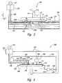
- FIG. 3is a partially schematic, side elevational view of an apparatus 160 for removing conductive material from a microelectronic substrate or substrate assembly 110 in accordance with an embodiment of the invention.
- the apparatus 160includes a vessel 130 containing an electrolyte 131 , which can be in a liquid or a gel state.
- electrolyte and electrolytic fluidrefer generally to electrolytic liquids and gels. Structures in fluid communication with electrolytic fluids are accordingly in fluid communication with electrolytic liquids or gels.
- the microelectronic substrate 110has an edge surface 112 and two face surfaces 113 .
- a support member 140supports the microelectronic substrate 110 relative to the vessel 130 so that a conductive layer 111 on at least one of the face surfaces 113 of the substrate 110 contacts the electrolyte 131 .
- the conductive layer 111can include metals such as platinum, tungsten, tantalum, gold, copper, rhodium, iridium, titanium or other conductive materials, such as doped polysilicon.
- the support member 140is coupled to a substrate drive unit 141 that moves the support member 140 and the substrate 110 relative to the vessel 130 .
- the substrate drive unit 141can translate the support member 140 (as indicated by arrow “A”) and/or rotate the support member 140 (as indicated by arrow “B”).
- the apparatus 160can further include a first electrode 120 a and a second electrode 120 b (referred to collectively as electrodes 120 ) supported relative to the microelectronic substrate 110 by a support member 124 .
- the support arm 124is coupled to an electrode drive unit 123 for moving the electrodes 120 relative to the microelectronic substrate 110 .
- the electrode drive unit 123can move the electrodes toward and away from the conductive layer 111 of the microelectronic substrate 110 , (as indicated by arrow “C”), and/or transversely (as indicated by arrow “D”) in a plane generally parallel to the conductive layer 111 .
- the electrode drive unit 123can move the electrodes in other fashions, or the electrode drive unit 123 can be eliminated when the substrate drive unit 141 provides sufficient relative motion between the substrate 110 and the electrodes 120 .
- the electrodes 120are coupled to a current source 121 with leads 128 for supplying electrical current to the electrolyte 131 and the conductive layer 111 .
- the current source 121supplies an alternating current (single phase or multiphase) to the electrodes 120 .
- the currentpasses through the electrolyte 131 and reacts electrochemically with the conductive layer 111 to remove material (for example, atoms or groups of atoms) from the conductive layer 111 .
- the electrodes 120 and/or the substrate 110can be moved relative to each other to remove material from selected portions of the conductive layer 111 , or from the entire conductive layer 111 .
- a distance D 1 between the electrodes 120 and the conductive layer 111is set to be smaller than a distance D 2 between the first electrode 120 a and the second electrode 120 b .
- the electrolyte 131generally has a higher resistance than the conductive layer 11 . Accordingly, the alternating current follows the path of least resistance from the first electrode 120 a , through the electrolyte 131 to the conductive layer 111 and back through the electrolyte 131 to the second electrode 120 b , rather than from the first electrode 120 a directly through the electrolyte 131 to the second electrode 120 b .
- a low dielectric material(not shown) can be positioned between the first electrode 120 a and the second electrode 120 b to decouple direct electrical communication between the electrodes 120 that does not first pass through the conductive layer 111 .
- One feature of an embodiment of the apparatus 160 shown in FIG. 3is that the electrodes 120 do not contact the conductive layer 111 of the substrate 110 .
- An advantage of this arrangementis that it can eliminate the residual conductive material resulting from a direct electrical connection between the electrodes 120 and the conductive layer 111 , described above with reference to FIGS. 1 and 2 .
- the apparatus 160can eliminate residual conductive material adjacent to the contact region between the electrodes and the conductive layer because the electrodes 120 do not contact the conductive layer 111 .
- the substrate 110 and/or the electrodes 120can move relative to the other to position the electrodes 120 at any point adjacent to the conductive layer 111 .
- An advantage of this arrangementis that the electrodes 120 can be sequentially positioned adjacent to every portion of the conductive layer to remove material from the entire conductive layer 111 . Alternatively, when it is desired to remove only selected portions of the conductive layer 111 , the electrodes 120 can be moved to those selected portions, leaving the remaining portions of the conductive layer 111 intact.
- FIG. 4is a partially schematic, side elevational view of an apparatus 260 that includes a support member 240 positioned to support the substrate 110 in accordance with another embodiment of the invention.
- the support member 240supports the substrate 110 with the conductive layer 111 facing upwardly.
- a substrate drive unit 241can move the support member 240 and the substrate 110 , as described above with reference to FIG. 3 .
- First and second electrodes 220 a and 220 bare positioned above the conductive layer 111 and are coupled to a current source 221 .
- a support member 224supports the electrodes 220 relative to the substrate 110 and is coupled to an electrode drive unit 223 to move the electrodes 220 over the surface of the support conductive layer 111 in a manner generally similar to that described above with reference to FIG. 3 .
- the apparatus 260further includes an electrolyte vessel 230 having a supply conduit 237 with an aperture 238 positioned proximate to the electrodes 220 .
- an electrolyte 231can be disposed locally in an interface region 239 between the electrodes 220 and the conductive layer 111 , without necessarily covering the entire conductive layer 111 .
- the electrolyte 231 and the conductive material removed from the conductive layer 111flow over the substrate 110 and collect in an electrolyte receptacle 232 .
- the mixture of electrolyte 231 and conductive materialcan flow to a reclaimer 233 that removes most of the conductive material from the electrolyte 231 .
- a filter 234 positioned downstream of the reclaimer 233provides additional filtration of the electrolyte 231 and a pump 235 returns the reconditioned electrolyte 231 to the electrolyte vessel 230 via a return line 236 .
- the apparatus 260can include a sensor assembly 250 having a sensor 251 positioned proximate to the conductive layer 111 , and a sensor control unit 252 coupled to the sensor 251 for processing signals generated by the sensor 251 .
- the control unit 252can also move the sensor 251 relative to the substrate 110 .
- the sensor assembly 250can be coupled via a feedback path 253 to the electrode drive unit 223 and/or the substrate drive unit 241 .
- the sensor 251can determine which areas of the conductive layer 111 require additional material removal and can move the electrodes 220 and/or the substrate 110 relative to each other to position the electrodes 220 over those areas.
- the electrodes 220 and/or the substrate 110can move relative to each other according to a pre-determined motion schedule.
- the sensor 251 and the sensor control unit 252can have any of a number of suitable configurations.
- the sensor 251can be an optical sensor that detects removal of the conductive layer 111 by detecting a change in the intensity, wavelength or phase shift of the light reflected from the substrate 110 when the conductive material is removed.
- the sensor 251can emit and detect reflections of radiation having other wavelengths, for example, x-ray radiation.
- the sensor 251can measure a change in resistance or capacitance of the conductive layer 111 between two selected points.
- one or both of the electrodes 220can perform the function of the sensor 251 (as well as the material removal function described above), eliminating the need for a separate sensor 251 .
- the sensor 251can detect a change in the voltage and/or current drawn from the current supply 221 as the conductive layer 111 is removed.
- the sensor 251can be positioned apart from the electrolyte 231 because the electrolyte 231 is concentrated in the interface region 239 between the electrodes 220 and the conductive layer 111 . Accordingly, the accuracy with which the sensor 251 determines the progress of the electrolytic process can be improved because the electrolyte 231 will be less likely to interfere with the operation of the sensor 251 . For example, when the sensor 251 is an optical sensor, the electrolyte 231 will be less likely to distort the radiation reflected from the surface of the substrate 110 because the sensor 251 is positioned away from the interface region 239 .
- Another feature of an embodiment of the apparatus 260 described above with reference to FIG. 4is that the electrolyte 231 supplied to the interface region 239 is continually replenished, either with a reconditioned electrolyte or a fresh electrolyte.
- An advantage of this featureis that the electrochemical reaction between the electrodes 220 and the conductive layer 111 can be maintained at a high and consistent level.
- FIG. 5is a partially schematic, side elevational view of an apparatus 360 that directs alternating current to the substrate 110 through a first electrolyte 331 a and a second electrolyte 331 b .
- the first electrolyte 331 ais disposed in two first electrolyte vessels 330 a
- the second electrolyte 331 bis disposed in a second electrolyte vessel 330 b .
- the first electrolyte vessels 330 aare partially submerged in the second electrolyte 331 b .
- the apparatus 360can further include electrodes 320 , shown as a first electrode 320 a and a second electrode 320 b , each coupled to a current supply 321 and each housed in one of the first electrolyte vessels 330 a .
- one of the electrodes 320can be coupled to ground.
- the electrodes 320can include materials such as silver, platinum, copper and/or other materials, and the first electrolyte 331 a can include sodium chloride, potassium chloride, copper sulfate and/or other electrolytes that are compatible with the material forming the electrodes 320 .
- the first electrolyte vessels 330 ainclude a flow restrictor 322 , such as a permeable isolation membrane formed from TeflonTM, sintered materials such as sintered glass, quartz or sapphire, or other suitable porous materials that allow ions to pass back and forth between the first electrolyte vessels 330 a and the second electrolyte vessel 330 b , but do not allow the second electrolyte 330 b to pass inwardly toward the electrodes 320 (for example, in a manner generally similar to a salt bridge).
- a flow restrictor 322such as a permeable isolation membrane formed from TeflonTM, sintered materials such as sintered glass, quartz or sapphire, or other suitable porous materials that allow ions to pass back and forth between the first electrolyte vessels 330 a and the second electrolyte vessel 330 b , but do not allow the second electrolyte 330 b to pass inwardly toward the electrodes 320 (for example, in a manner generally similar to
- the first electrolyte 331 acan be supplied to the electrode vessels 330 a from a first electrolyte source 339 at a pressure and rate sufficient to direct the first electrolyte 331 a outwardly through the flow restrictor 322 without allowing the first electrolyte 331 a or the second electrolyte 330 b to return through the flow restrictor 322 .
- the second electrolyte 331 bremains electrically coupled to the electrodes 320 by the flow of the first electrolyte 331 a through the restrictor 322 .
- the apparatus 360can also include a support member 340 that supports the substrate 110 with the conductive layer 111 facing toward the electrodes 320 .
- the support member 340can be positioned in the second electrolyte vessel 330 b .
- the support member 340 and/or the electrodes 320can be movable relative to each other by one or more drive units (not shown).
- the first electrolyte 331 acan be selected to be compatible with the electrodes 320 .
- An advantage of this featureis that the first electrolyte 331 a can be less likely than conventional electrolytes to degrade the electrodes 320 .
- the second electrolyte 331 bcan be selected without regard to the effect it has on the electrodes 320 because it is chemically isolated from the electrodes 320 by the flow restrictor 322 .
- the second electrolyte 331 bcan include hydrochloric acid or another agent that reacts aggressively with the conductive layer 111 of the substrate 110 .
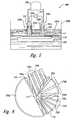
- FIG. 6is a top plan view of the microelectronic substrate 110 positioned beneath a plurality of electrodes having shapes and configurations in accordance with several embodiments of the invention. For purposes of illustration, several different types of electrodes are shown positioned proximate to the same microelectronic substrate 110 ; however, in practice, electrodes of the same type can be positioned relative to a single microelectronic substrate 110 .
- electrodes 720 a and 720 bcan be grouped to form an electrode pair 770 a , with each electrode 720 a and 720 b coupled to an opposite terminal of a current supply 121 ( FIG. 3 ).
- the electrodes 770 a and 770 bcan have an elongated or strip-type shape and can be arranged to extend parallel to each other over the diameter of the substrate 110 .
- the spacing between adjacent electrodes of an electrode pair 370 acan be selected to direct the electrical current into the substrate 110 , as described above with reference to FIG. 3 .
- electrodes 720 c and 720 dcan be grouped to form an electrode pair 770 b , and each electrode 720 c and 720 d can have a wedge or “pie” shape that tapers inwardly toward the center of the microelectronic substrate 110 .
- narrow, strip-type electrodes 720 e and 720 fcan be grouped to form electrode pairs 770 c , with each electrode 720 e and 720 f extending radially outwardly from the center 113 of the microelectronic substrate 110 toward the periphery 112 of the microelectronic substrate 110 .
- a single electrode 720 gcan extend over approximately half the area of the microelectronic substrate 110 and can have a semicircular planform shape.
- the electrode 720 gcan be grouped with another electrode (not shown) having a shape corresponding to a mirror image of the electrode 720 g , and both electrodes can be coupled to the current source 121 to provide alternating current to the microelectronic substrate in any of the manners described above with reference to FIGS. 3-5 .
- FIG. 7is a partially schematic, cross-sectional side elevational view of a portion of the substrate 110 positioned beneath the electrode 720 c described above with reference to FIG. 6 .
- the electrode 720 chas an upper surface 771 and a lower surface 772 opposite the upper surface 771 and facing the conductive layer 111 of the substrate 110 .
- the lower surface 772can taper downwardly from the center 113 of the substrate 110 toward the perimeter 112 of the substrate 110 in one aspect of this embodiment to give the electrode 720 c a wedge-shaped profile.
- the electrode 720 ccan have a plate-type configuration with the lower surface 772 positioned as shown in FIG. 7 and the upper surface 771 parallel to the lower surface 772 .
- the electrical coupling between the electrode 720 c and the substrate 110can be stronger toward the periphery 112 of the substrate 110 than toward the center 113 of the substrate 110 .
- This featurecan be advantageous when the periphery 112 of the substrate 110 moves relative to the electrode 720 c at a faster rate than does the center 113 of the substrate 110 , for example, when the substrate 110 rotates about its center 113 .
- the electrode 720 ccan be shaped to account for relative motion between the electrode and the substrate 110 .
- the electrode 720 ccan have other shapes.
- the lower surface 772can have a curved rather than a flat profile.
- any of the electrodes described above with reference to FIG. 6(or other electrodes having shapes other than those shown in FIG. 6 ) can have a sloped or curved lower surface.
- the electrodescan have other shapes that account for relative motion between the electrodes and the substrate 110 .
- FIG. 8Ais a partially schematic view of an electrode support 473 for supporting a plurality of electrodes in accordance with another embodiment of the invention.
- the electrode support 473can include a plurality of electrode apertures 474 , each of which houses either a first electrode 420 a or a second electrode 420 b .
- the first electrodes 420 aare coupled through the apertures 474 to a first lead 428 a and the second electrodes 420 b are coupled to a second lead 428 b .
- Both of the leads 428 a and 428 bare coupled to a current supply 421 .
- each pair 470 of first and second electrodes 420 a and 420 bdefines part of a circuit that is completed by the substrate 110 and the electrolyte(s) described above with reference to FIGS. 3-5 .
- the first lead 428 acan be offset from the second lead 428 b to reduce the likelihood for short circuits and/or capacitive coupling between the leads.
- the electrode support 473can have a configuration generally similar to any of those described above with reference to FIGS. 1-7 .
- any of the individual electrodese.g., 320 a , 320 c , 320 e , or 320 g ) described above with reference to FIG. 6 can be replaced with an electrode support 473 having the same overall shape and including a plurality of apertures 474 , each of which houses one of the first electrodes 420 a or the second electrodes 420 b.
- the electrode pairs 470 shown in FIG. 8Acan be arranged in a manner that corresponds to the proximity between the electrodes 420 a , 420 b and the microelectronic substrate 110 ( FIG. 7 ), and/or the electrode pairs 470 can be arranged to correspond to the rate of relative motion between the electrodes 420 a , 420 b and the microelectronic substrate 110 .
- the electrode pairs 470can be more heavily concentrated in the periphery 112 of the substrate 110 or other regions where the relative velocity between the electrode pairs 470 and the substrate 110 is relatively high (see FIG. 7 ). Accordingly, the increased concentration of electrode pairs 470 can provide an increased electrolytic current to compensate for the high relative velocity.
- first electrode 420 a and the second electrode 420 b of each electrode pair 470can be relatively close together in regions (such as the periphery 112 of the substrate 110 ) where the electrodes are close to the conductive layer 111 (see FIG. 7 ) because the close proximity to the conductive layer 111 reduces the likelihood for direct electrical coupling between the first electrode 420 a and the second electrode 420 b .
- the amplitude, frequency and/or waveform shape supplied to different electrode pairs 470can vary depending on factors such as the spacing between the electrode pair 470 and the microelectronic substrate 110 , and the relative velocity between the electrode pair 470 and the microelectronic substrate 110 .
- FIGS. 8B and 8Cillustrate electrodes 820 (shown as first electrodes 820 a and second electrodes 820 b ) arranged concentrically in accordance with still further embodiments of the invention.
- the first electrode 820 acan be positioned concentrically around the second electrode 820 b , and a dielectric material 829 can be disposed between the first electrode 820 a and the second electrode 820 b .
- the first electrode 820 acan define a complete 360° arc around the second electrode 820 b , as shown in FIG. 8B , or alternatively, the first electrode 820 a can define an arc of less than 360°.
- the first electrode 820 acan be concentrically disposed between two second electrodes 820 b , with the dielectric material 829 disposed between neighboring electrodes 820 .
- currentcan be supplied to each of the second electrodes 820 b with no phase shifting.
- the current supplied to one second electrode 820 bcan be phase-shifted relative to the current supplied to the other second electrode 820 b .
- the current supplied to each second electrode 820 bcan differ in characteristics other than phase, for example, amplitude.
- the first electrode 820 acan shield the second electrode(s) 820 b from interference from other current sources.
- the first electrode 820 acan be coupled to ground to shield the second electrodes 820 b .
- An advantage of this arrangementis that the current applied to the substrate 110 ( FIG. 7 ) via the electrodes 820 can be more accurately controlled.
- FIG. 9schematically illustrates an apparatus 560 for chemically, mechanically and/or electrolytically processing the microelectronic substrate 110 in accordance with an embodiment of the invention.
- the apparatus 560has a support table 580 with a top-panel 581 at a workstation where an operative portion “W” of a polishing pad 582 is positioned.
- the top-panel 581is generally a rigid plate to provide a flat, solid surface to which a particular section of the polishing pad 582 may be secured during material removal processes.
- the apparatus 560can also have a plurality of rollers to guide, position and hold the polishing pad 582 over the top-panel 581 .
- the rollerscan include a supply roller 583 , first and second idler rollers 584 a and 584 b , first and second guide rollers 585 a and 585 b , and a take-up roller 586 .
- the supply roller 583carries an unused or pre-operafive portion of the polishing pad 582
- the take-up roller 583carries a used or post-operative portion of the polishing pad 582 .
- first idler roller 584 a and the first guide roller 585 acan stretch the polishing pad 582 over the top-panel 581 to hold the polishing pad 582 stationary during operation.
- a motor(not shown) drives at least one of the supply roller 583 and the take-up roller 586 to sequentially advance the polishing pad 582 across the top-panel 581 . Accordingly, clean pre-operative sections of the polishing pad 582 may be quickly substituted for used sections to provide a consistent surface for polishing and/or cleaning the substrate 110 .
- the apparatus 560can also have a carrier assembly 590 that controls and protects the substrate 110 during the material removal processes.
- the carrier assembly 590can include a substrate holder 592 to pick up, hold and release the substrate 110 at appropriate stages of the material removal process.
- the carrier assembly 590can also have a support gantry 594 carrying a drive assembly 595 that can translate along the gantry 594 .
- the drive assembly 595can have an actuator 596 , a drive shaft 597 coupled to the actuator 596 , and an arm 598 projecting from the drive shaft 597 .
- the arm 598carries the substrate holder 592 via a terminal shaft 599 such that the drive assembly 595 orbits the substrate holder 592 about an axis E-E (as indicated by arrow “R 1 ”).
- the terminal shaft 599may also rotate the substrate holder 592 about its central axis F-F (as indicated by arrow “R 2 ”).
- the polishing pad 582 and a planarizing solution 587define at least a portion of a material removal medium that mechanically and/or chemically-mechanically removes material from the surface of the substrate 110 .
- the polishing pad 582 used in the apparatus 560can be a fixed-abrasive polishing pad having abrasive particles that are fixedly bonded to a suspension medium.
- the planarizing solution 587can be a “clean solution” without abrasive particles because the abrasive particles are fixedly distributed across a polishing surface 588 of the polishing pad 582 .
- the polishing pad 582may be a non-abrasive pad without abrasive particles
- the planarizing solution 587can be a slurry with abrasive particles and chemicals to remove material from the substrate 110 .
- both the polishing pad 582 and the planarizing solution 587can be configured without abrasive particles or elements, as described in greater detail below with reference to FIGS. 9-11 .
- the carrier assembly 590presses the face 113 of the substrate 110 against the polishing surface 588 of the polishing pad 582 in the presence of the planarizing solution 587 .
- the drive assembly 595then orbits the substrate holder 592 about the axis E-E and optionally rotates the substrate holder 592 about the axis F-F to translate the substrate 110 across the planarizing surface 588 .
- the abrasive particles and/or the chemicals in the material removal mediumremove material from the surface of the substrate 110 in a chemical and/or chemical-mechanical planarization (CMP) process.
- CMPchemical-mechanical planarization
- the polishing pad 582can smooth the substrate 110 by removing rough features projecting from the conductive layer 111 of the substrate 110 .
- the apparatus 560can include an electrolyte supply vessel 530 that delivers an electrolyte to the planarizing surface 588 of the polishing pad 582 with a conduit 537 , as described in greater detail with reference to FIG. 10 .
- the apparatus 560can further include a current supply 521 coupled to the support table 580 and/or the top-panel 581 to supply an electrical current to electrodes positioned in the support table 580 and/or the top-panel 581 . Accordingly, the apparatus 560 can electrolytically remove material from the conductive layer 111 in a manner similar to that described above with reference to FIGS. 1-8C .
- materialcan be sequentially removed from the conductive layer 111 of the substrate 110 first by an electrolytic process and then by a CMP process.
- the electrolytic processcan remove material from the conductive layer 111 in a manner that roughens the conductive layer 111 .
- the electrolytic processing operationcan be halted and additional material can be removed via CMP processing.
- the electrolytic process and the CMP processcan be conducted simultaneously.
- one feature of an embodiment of the apparatus 560 described above with reference to FIG. 9is that the same apparatus 560 can planarize the substrate 110 via CMP and remove material from the substrate 110 via an electrolytic process.
- An advantage of this arrangementis that the substrate 110 need not be moved from one apparatus to another to undergo both CMP and electrolytic processing.
- Another advantage of an embodiment of the apparatus 560 described above with reference to FIG. 9is that the processes, when used in conjunction with each other, are expected to remove material from the substrate 110 more quickly and accurately than some conventional processes.
- the electrolytic processcan remove relatively large amounts of material in a manner that roughens the microelectronic substrate 110
- the planarizing processcan remove material on a finer scale in a manner that smoothes and/or flattens the microelectronic substrate 110 .
- FIG. 10is a partially exploded, partially schematic isometric view of a portion of the apparatus 560 described above with reference to FIG. 9 .
- the top-panel 581houses a plurality of electrode pairs 570 , each of which includes a first electrode 520 a and a second electrode 520 b .
- the first electrodes 520 aare coupled to a first lead 528 a and the second electrodes 520 b are coupled to a second lead 528 b .
- the first and second leads 528 a and 528 bare coupled to the current source 521 ( FIG. 9 ).
- the first electrode 520 acan be separated from the second electrodes 520 b by an electrode dielectric layer 529 a that includes TeflonTM or another suitable dielectric material.
- the electrode dielectric layer 529 acan accordingly control the volume and dielectric constant of the region between the first and second electrodes 520 a and 520 b to control electrical coupling between the electrodes.
- the electrodes 520 a and 520 bcan be electrically coupled to the microelectronic substrate 110 ( FIG. 9 ) by the polishing pad 582 .
- the polishing pad 582is saturated with an electrolyte 531 supplied by the supply conduits 537 through apertures 538 in the top-panel 581 just beneath the polishing pad 582 .
- the electrodes 520 a and 520 bare selected to be compatible with the electrolyte 531 .
- the electrolyte 531can be supplied to the polishing pad 582 from above (for example, by disposing the electrolyte 531 in the planarizing liquid 587 ) rather than through the top-panel 581 .
- the polishing pad 582can include a pad dielectric layer 529 b positioned between the polishing pad 582 and the electrodes 520 a and 520 b .
- the electrodes 520 a and 520 bare isolated from physical contact with the electrolyte 531 and can accordingly be selected from materials that are not necessarily compatible with the electrolyte 531 .
- the electrodes 520 a and 520 bcan be in fluid communication with each other and the conductive layer 111 via a common volume of electrolyte 531 .
- Each electrode 520 a , 520 bcan be more directly electrically coupled to the conductive layer 111 ( FIG. 9 ) than to the other electrode so that electrical current passes from one electrode through the conductive layer 111 to the other electrode.
- the electrodes 520 a and 520 bface toward the face surface 113 ( FIG. 9 ) of the microelectronic substrate 110 , with the polishing pad 582 interposed between the electrodes 520 a and 520 b and the face surface 113 .
- the electrodescan electrically couple to at least a substantial portion of the face surface 113 . Accordingly, the likelihood for forming electrically isolated “islands” in the conductive layer 111 ( FIG. 9 ) at the face surface 113 can be reduced when compared to conventional devices.
- the apparatusincludes only two electrodes, each configured to face toward about one-half of the face surface 113 (in a manner generally similar to that described above with reference to electrode 220 g of FIG. 6 ), then the electrodes can also electrically coupled to at least a substantial portion of the face surface 113 .
- the polishing pad 582can provide several additional advantages over some conventional electrolytic arrangements.
- the polishing pad 582can uniformly separate the electrodes 520 a and 520 b from the microelectronic substrate 110 ( FIG. 9 ), which can increase the uniformity with which the electrolytic process removes material from the conductive layer 111 ( FIG. 9 ).
- the polishing pad 582can also have abrasive particles 589 for planarizing the microelectronic substrate 110 in the manner described above with reference to FIG. 9 .
- the polishing pad 582can filter carbon or other material that erodes from the electrodes 520 a and 520 b to prevent the electrode material from contacting the microelectronic substrate 110 . Still further, the polishing pad 582 can act as a sponge to retain the electrolyte 531 in close proximity to the microelectronic substrate 110 .
- FIG. 11is a partially schematic, cross-sectional side elevational view of a rotary apparatus 660 for mechanically, chemically and/or electrolytically processing the microelectronic substrate 110 in accordance with another embodiment of the invention.
- the apparatus 660has a generally circular platen or table 680 , a carrier assembly 690 , a polishing pad 682 positioned on the table 680 , and a planarizing liquid 687 on the polishing pad 682 .
- the polishing pad 682can be a fixed abrasive polishing pad or, alternatively, the planarizing liquid 687 can be a slurry having a suspension of abrasive elements and the polishing pad 682 can be a non-abrasive pad.
- a drive assembly 695rotates (arrow “G”) and/or reciprocates (arrow “H”) the platen 680 to move the polishing pad 682 during planarization.
- the motion of the microelectronic substrate 110 relative to the polishing pad 682can include circular, elliptical, orbital, precessional or non-precessional motions.
- the carrier assembly 690controls and protects the microelectronic substrate 110 during the material removal process.
- the carrier assembly 690typically has a substrate holder 692 with a pad 694 that holds the microelectronic substrate 110 via suction.
- a drive assembly 696 of the carrier assembly 690typically rotates and/or translates the substrate holder 692 (arrows “I” and “J,” respectively).
- the substrate holder 692may include a weighted, free-floating disk (not shown) that slides over the polishing pad 682 .
- the carrier assembly 690presses the microelectronic substrate 110 against a polishing surface 688 of the polishing pad 682 .
- the platen 680 and/or the substrate holder 692then move relative to one another to translate the microelectronic substrate 110 across the polishing surface 688 .
- the abrasive particles in the polishing pad 682 and/or the chemicals in the planarizing liquid 687remove material from the surface of the microelectronic substrate 110 .
- the apparatus 660can also include a current source 621 coupled with leads 628 a and 628 b to one or more electrode pairs 670 (one of which is shown in FIG. 11 ).
- the electrode pairs 670can be integrated with the platen 680 in generally the same manner with which the electrodes 520 a and 520 b ( FIG. 10 ) are integrated with the top panel 581 ( FIG. 10 ).
- the electrode pairs 670can be integrated with the polishing pad 682 .
- the electrode pairs 670can include electrodes having shapes and configurations generally similar to any of those described above with reference to FIGS. 3-10 to electrolytically remove conductive material from the microelectronic substrate 110 .
- the electrolytic processcan be carried out before, during or after the CMP process, as described above with reference to FIG. 9 .
- the apparatuses described above with reference to FIGS. 3-11can be used in accordance with other methods.
- the electrolytic processcan be used in addition to or in lieu of direct chemical interactions to oxidize conductive (including semiconductive) portions of the microelectronic substrate 110 .
- the electrolytic processcan oxidize metals (such as platinum, rhodium, iridium, or gold) that are normally difficult or nearly impracticable to oxidize.
- metalssuch as platinum, rhodium, iridium, or gold
- platinum and other noble metals that resist oxidationare generally difficult to remove from the microelectronic substrate 110 without employing an isotropic etching chemical (i.e., a chemical that etches indiscriminately in all directions) and/or a very high downforce applied to the microelectronic substrate by the polishing pad 682 .
- the electrolytic processcan anisotropically oxidize the platinum (or other conductive material) generally in a direction normal to the polishing surface 688 of the polishing pad 682 .
- the conductive materialcan be removed from the microelectronic substrate 110 .
- the electrolytic oxidation processroughens the surface of the conductive material and penetrates only a short distance beneath the surface.
- the oxidized materialcan then be removed by chemical and/or mechanical interactions with the polishing pad and/or planarizing solution.
- the downforce required to remove the oxidized materialcan be less than the downforce required by techniques that do not include an electrolytic process. In one specific example, it has been determined that a pressure of approximately 0.2 psi will remove 1,000 angstroms of platinum in ten minutes using an embodiment of the invention, whereas it is typically not possible to anisotropically remove platinum at any rate using conventional CMP techniques.
- the apparatuses described above with reference to FIGS. 9-11can oxidize and remove materials other than platinum at higher rates and/or with lower downforces than are typically required with conventional CMP apparatuses.
- An advantage of increasing the rate with which conductive material can be oxidized and removed from the microelectronic substrates 110is that the throughput of microelectronic substrates 110 can be increased when compared to conventional techniques.
- An advantage of anisotropically oxidizing and removing the conductive material from the microelectronic substrates 110is that this technique can remove over-layers of the conductive material without undercutting adjacent structures in a lateral direction. Accordingly, methods in accordance with embodiments of the invention can more reliably form vias, conductive lines, and other conductive structures in the microelectronic substrate 110 .
- An advantage of reducing the downforce applied to the microelectronic substrate 110 during processingis that this technique can reduce the likelihood for damaging the microelectronic substrate 110 and can increase the life expectancy of the apparatus applying the downforce.
- the characteristics of the electrical signal applied to the microelectronic substrate 110can be selected to control the rate and/or manner with which the material is removed from the microelectronic substrate 110 .
- the amplitude of the electrical currentcan be increased to increase the rate at which the conductive material oxidizes, and accordingly, the rate at which the oxidized material is available for removal.
- the amplitude of the electrical currentcan be reduced to reduce the oxidation rate.
- the currentcan be halted to control the rate at which conductive material is removed from the microelectronic substrate 110 .
- the current amplitudecan be varied from about 1 amp to about 10 amps, depending upon the desired oxidation and removal rate, and depending upon the type of material removed from the microelectronic substrate 110 .
- the voltage applied to the materialcan be increased or decreased to increase or decrease, respectively, the material oxidation and removal rates.
- the voltagecan be varied up to about 100 volts.
- the frequency with which the electrical signal is appliedcan be varied to control the material oxidation and removal rate.
- a potential of about 10 volts rmscan be applied to a platinum layer of the microelectronic substrate at a frequency of about 60 Hz while the microelectronic substrate 110 is engaged with the polishing pad 582 to anisotropically remove a portion of the platinum from the microelectronic substrate 110 .
- the polishing pad 582can be a conventional pad, such as an IC 1000 polishing pad (available from Rodell, Inc. of Phoenix, Ariz.).
- the polishing pad 582can have abrasive elements fixedly distributed in a suspension medium.
- the abrasive elementscan be suspended in a planarizing liquid or slurry disposed between the polishing pad 582 and the microelectronic substrate 110 .
- the abrasive elementscan include chromium dioxide, aluminum oxide or silicon dioxide, and the planarizing liquid can include an electrolyte to electrically couple the microelectronic substrate to a source of electrical potential.
- the abrasive elementscan be eliminated entirely from the material removal medium, and the material can be removed from the microelectronic substrate 110 as a result of the electrolytic process and contact with the polishing pad 582 .
- the electrical-mechanical interaction described abovecan be supplemented with a chemical interaction by exposing the microelectronic substrate 110 to one or more chemically reactive liquid solutions.
- the chemical solutionscan be generally similar to those typically used for CMP processing.
- the chemical solutions, the chemical environment, and the chemical interactionscan be different than those associated with conventional CMP techniques.
- the solutioncan include an electrolytic fluid having (NH 4 ) 2 SO 4 , H 2 SO 4 , K 2 SO 4 , MgSO 4 , and/or H 3 PO 4 .
- the fluidcan have other constituents, such as those described below with reference to FIGS. 13 A-C.
- the fluidcan also include a relatively low concentration of chloride ions (e.g., from about 50 ppm to about 5,000 ppm for copper removal, and from about 100 ppm to about 5,000 ppm for platinum removal).
- the liquidcan include a mixture of (NH) 2 SO 4 at a concentration of from about 1M (moles/liter) to about 5.5M, H 2 SO 4 at a concentration of up to about 0.5M, and about 500 ppm chloride ions. This is unlike typical planarizing liquids that include chlorine-based substances (such as KCl or HCl) and have much higher concentrations of chloride ions (for example, about 100,000 ppm).
- an advantage of the chemical solutions described aboveis that they can more effectively remove materials, such as platinum, that are otherwise difficult to remove from the microelectronic substrate 110 . It is believed that in one aspect of this embodiment, the chloride ions' can adsorb to the metal surface and roughen the exposed surface of the conductive material, making the conductive material easier to remove from the microelectronic substrate.
- the pH of the environmentcan have any value from about 1 up to about 14.
- the pH of the environmentcan be from about 1 to about 14, or, in a specific embodiment, less than about 3 or greater than about 10.
- the pH of liquid typically used to planarize tungstenhas a range from about 3 to about 4
- the liquid in accordance with another aspect of the inventioncan have a pH of less than about 3 or greater than about 4.
- the pH of a liquid typically used to planarize copperis about 7
- the pH of a liquid in accordance with another aspect of the inventioncan have a pH of less than about 6 or greater than about 8.
- FIGS. 12 A-Bschematically illustrate applying the foregoing methods and apparatuses to removing semiconductor material 1211 from a microelectronic substrate 1210 in accordance with an embodiment of the invention.
- the microelectronic substrate 1210can include a substrate material 1215 having a recess 1212 in which the semiconductor material 1211 is disposed.
- the substrate materialcan include a borophosphate silicon glass (BPSG) or another substrate material.
- the semiconductor material 1211can include polysilicon doped with phosphorous or boron, and in other embodiments, the semiconductor material 1211 can include other compositions.
- the semiconductor material 1211can have a recessed surface 1214 a directly over the recess 1212 .
- a portion of the semiconductor material 1211can be removed to form a flat surface 1214 b ( FIG. 12 b ) by electrolytically oxidizing the semiconductor material 1211 and removing the semiconductor material 1211 with chemical and/or mechanical forces, generally as described above.
- Conventional techniques for removing doped polysiliconinclude planarizing the polysilicon with a slurry having a pH of from about 10.5 to about 11.5.
- the conventional slurrytypically includes tetramethyl ammonium hydroxide (TMAH) and a suspension of silicon dioxide abrasive particles.
- TMAHtetramethyl ammonium hydroxide
- An advantage of a method for removing polysilicon and other semiconductor materials in accordance with an embodiment of the inventionis that the material can be removed without the use of abrasive elements, and the material can be removed using an electrolytic fluid having a pH less than 10.5 or greater than 11.5. Accordingly, the user can select electrolytic fluids (such as those described above) having a wider variety of pHs than are conventionally used.
- the electrolytic fluidcan include dilute hydrofluoric acid or a combination of ammonium hydroxide and TMAH.
- the voltage applied to the semiconductor material 1211can range from about 25 volts rms to about 100 volts rms, for phosphorous-doped polysilicon.
- the electrolytic fluidcan include a mixture of hydrofluoric acid and TMAH, and the voltage applied to the semiconductor material can be approximately the same as that discussed above for phosphorous-doped polysilicon.
- a further advantage of a method in accordance with an embodiment of the inventionis that the electrolytic fluid selected to remove the semiconductor material 1211 from the microelectronic substrate 1210 can be selected to have little or no chemical interaction with the substrate material 1215 . Accordingly, for applications in which the semiconductor material 1211 is removed down to the level of the substrate material 1215 , the removal process can automatically stop (i.e., endpoint) when the substrate material 1215 is exposed. Accordingly, the process can eliminate other more cumbersome and/or less accurate conventional endpointing techniques.
- FIGS. 13 A-Cschematically illustrate methods for applying the foregoing techniques and apparatuses to removing a first conductive material 1311 and a second conductive material 1317 from a microelectronic substrate 1310 .
- the microelectronic substrate 1310can include a substrate material 1315 having a dielectric portion 1316 (such as an oxide layer) with recesses 1312 or other features formed in the dielectric portion 1316 .
- the second conductive material 1317is disposed in the recesses 1312 and on the dielectric portion 1316 (for example, in the form of a barrier layer), and the first conductive material 1311 is disposed on the second conductive material 1317 .
- the first conductive material 1311can include copper and the second conductive material 1317 can include tantalum, tantalum nitride, tungsten, tungsten nitride, titanium, titanium nitride, titanium silicon nitride, and/or tantalum silicon nitride.
- the first and second conductive materials 1311 , 1317can include other compositions.
- the first conductive material 1311can be removed down to the level of the second conductive material 1317 using any of the devices described above with reference to FIGS. 9-11 .
- the electrolytic fluid used to remove the first conductive material 1311can include dilute H 3 PO 4 , or an organic acid, such as ammonium citrate.
- the electrolytic liquidcan include chloride ions in concentrations generally similar to those described above.
- the concentration of the chloride ionscan be used to control the rate at which the first conductive material 1311 is removed.
- the peak removal ratecan be achieved with a selected concentration of chloride ions that depends upon the other constituents of the electrolytic fluid and the composition of the first conductive material 1311 .
- the material removal ratecan decrease with either an increase or a decrease in the concentration of chloride ions from the selected concentration.
- an alcoholsuch as isopropyl alcohol or acetone
- the downforce applied to the first conductive material 1311 by the polishing padcan vary from less than 1 psi to several psi.
- the material of the electrode positioned at least proximate to the first conductive material 1311can include platinum or graphite, and the potential applied to the electrodes can vary from about 1 volt to about 15 volts, depending upon the composition of the electrolytic liquid.
- the chemical interaction with the first conductive material 1311can include an etching process, a complexing process, and/or a chelating process.
- the second conductive material 1317can be removed down to the level of the dielectric portion 1316 using methods and apparatuses generally similar to those described above.
- the electrolytic fluid disposed on the second conductive material 1317can include dilute hydrochloric acid, NH 4 Cl, and/or dilute phosphoric acid, or any organic or inorganic acid.
- the electrolytic fluidcan include a corrosion inhibitor to inhibit corrosion of the exposed first conductive material 1311 .
- the corrosion inhibitorcan include BTA.
- the electrodes positioned proximate to the second conductive material 1317can include graphite, and the voltage applied to the electrodes can be approximately the same as the voltage applied to the first conductive material 1311 .
- the voltage applied to the second conductive material 1317can be different.
- the downforce applied to the second conductive material 1317can be the same as the downforce applied to the first conductive material 1311 , and alternatively, the downforce applied to the second conductive material 1317 can be different than the downforce applied to the first conductive material 1311 .
- the process for removing the second conductive material 1317can automatically stop when the polishing pad engages the initially buried dielectric portion 1316 . Accordingly, an advantage of a method in accordance with an embodiment of the invention is that terminating the process for removing the second conductive material 1317 can be simpler than conventional techniques because a step specifically directed to endpointing is not required.
- the downforce applied to the microelectronic substrate 1310 while the first conductive material 1311 and the second conductive material 1317 are removedcan be less than the downforces applied during conventional CMP operations (i.e., CMP operations that do not include electrolytically oxidizing the first and second conductive materials).
- CMP operationsi.e., CMP operations that do not include electrolytically oxidizing the first and second conductive materials.
- an advantage of this featureis that the apparatus applying the downforce can have a longer life span.
- the lower downforcemay be less likely than conventional downforces to damage the substrate material 1315 and/or structures formed in the substrate material 1315 prior to applying the downforce. This feature may be particularly advantageous when the substrate material 1315 has a low dielectric constant, for example, a dielectric constant of from about 1.5 to about 3.0.
- Such materialscan include porous silica.
- FIG. 14Ais a schematic circuit representation of some of the components described above with reference to FIG. 10 .
- the circuit analogycan also apply to any of the arrangements described above with reference to FIGS. 3-13C .
- the current source 521is coupled to the first electrode 520 a and the second electrode 520 b with leads 528 a and 528 b , respectively.
- the electrodes 520 a and 520 bare coupled to the microelectronic substrate 110 with the electrolyte 531 in an arrangement that can be represented schematically by two sets of parallel capacitors and resistors.
- a third capacitor and resistorschematically indicates that the microelectronic substrate 110 “floats” relative to ground or another potential.
- the current source 521can be coupled to an amplitude modulator 522 that modulates the signal produced by the current source 521 , as is shown in FIG. 14B .
- the current source 521can generate a high-frequency wave 1404
- the amplitude modulator 522can superimpose a low-frequency wave 1402 on the high-frequency wave 1404 .
- the high-frequency wave 1404can include a series of positive or negative voltage spikes contained within a square wave envelope defined by the low-frequency wave 1402 . Each spike of the high-frequency wave 1404 can have a relatively steep rise time slope to transfer charge through the dielectric to the electrolyte, and a more gradual fall time slope.
- the fall time slopecan define a straight line, as indicated by high-frequency wave 1404 , or a curved line, as indicated by high-frequency wave 1404 a .
- the high-frequency wave 1404 and the low-frequency wave 1402can have other shapes depending, for example, on the particular characteristics of the dielectric material and electrolyte adjacent to the electrodes 420 , the characteristics of the substrate 110 , and/or the target rate at which material is to be removed from the substrate 110 .
- any of the embodiments described above with reference to FIGS. 3-13Ccan include an amplitude modulator in addition to a current source.
Landscapes
- Engineering & Computer Science (AREA)
- Chemical & Material Sciences (AREA)
- Mechanical Engineering (AREA)
- Chemical Kinetics & Catalysis (AREA)
- Electrochemistry (AREA)
- Physics & Mathematics (AREA)
- Metallurgy (AREA)
- Organic Chemistry (AREA)
- Materials Engineering (AREA)
- Condensed Matter Physics & Semiconductors (AREA)
- General Physics & Mathematics (AREA)
- Manufacturing & Machinery (AREA)
- Computer Hardware Design (AREA)
- Microelectronics & Electronic Packaging (AREA)
- Power Engineering (AREA)
- Weting (AREA)
- Mechanical Treatment Of Semiconductor (AREA)
Abstract
Description
- The present application is a continuation-in-part of U.S. application Ser. No. 09/651,779 (attorney docket number 108298515US), titled “Methods and Apparatus for Removing Conductive Material From a Microelectronic Substrate,” filed Aug. 30, 2000, U.S. application Ser. No. ______ (attorney docket number 108298515US2), titled “Microelectronic Substrate Having Conductive Material with Blunt Cornered Apertures, and Associated Methods for Removing Conductive Material,” filed concurrently herewith, and U.S. application Ser. No. ______ (attorney docket number 108298515US3), titled “Methods and Apparatus for Electrically and/or Chemically-Mechanically Removing Conductive Material from a Microelectronic Substrate,” filed concurrently herewith, all of which are incorporated herein in their entireties by reference.
- This invention relates to methods and apparatuses for removing conductive material from microelectronic substrates.
- Microelectronic substrates and substrate assemblies typically include a semiconductor material having features, such as memory cells, that are linked with conductive lines. The conductive lines can be formed by first forming trenches or other recesses in the semiconductor material, and then overlaying a conductive material (such as a metal) in the trenches. The conductive material is then selectively removed to leave conductive lines extending from one feature in the semiconductor material to another.
- Electrolytic techniques have been used to both deposit and remove metallic layers from semiconductor substrates. For example, an alternating current can be applied to a conductive layer via an intermediate electrolyte to remove portions of the layer. In one arrangement, shown in
FIG. 1 , aconventional apparatus 60 includes afirst electrode 20aand asecond electrode 20bcoupled to acurrent source 21. Thefirst electrode 20ais attached directly to ametallic layer 11 of asemiconductor substrate 10 and thesecond electrode 20bis at least partially immersed in aliquid electrolyte 31 disposed on the surface of themetallic layer 11 by moving the second electrode downwardly until it contacts theelectrolyte 31. Abarrier 22 protects thefirst electrode 20afrom direct contact with theelectrolyte 31. Thecurrent source 21 applies alternating current to thesubstrate 10 via theelectrodes electrolyte 31 to remove conductive material from theconductive layer 11. The alternating current signal can have a variety of wave forms, such as those disclosed by Frankenthal et al. in a publication entitled, “Electroetching of Platinum in the Titanium-Platinum-Gold Metallization on Silicon Integrated Circuits” (Bell Laboratories), incorporated herein in its entirety by reference. - One drawback with the arrangement shown in
FIG. 1 is that it may not be possible to remove material from theconductive layer 11 in the region where thefirst electrode 20ais attached because thebarrier 22 prevents theelectrolyte 31 from contacting thesubstrate 10 in this region. Alternatively, if thefirst electrode 20acontacts the electrolyte in this region, the electrolytic process can degrade thefirst electrode 20a. Still a further drawback is that the electrolytic process may not uniformly remove material from thesubstrate 10. For example, “islands” of residual conductive material having no direct electrical connection to thefirst electrode 20amay develop in theconductive layer 11. The residual conductive material can interfere with the formation and/or operation of the conductive lines, and it may be difficult or impossible to remove with the electrolytic process unless thefirst electrode 20ais repositioned to be coupled to such “islands.” - One approach to addressing some of the foregoing drawbacks is to attach a plurality of
first electrodes 20aaround the periphery of thesubstrate 10 to increase the uniformity with which the conductive material is removed. However, islands of conductive material may still remain despite the additionalfirst electrodes 20a. Another approach is to form theelectrodes barrier 22 to increase the area of theconductive layer 11 in contact with theelectrolyte 31. However, such inert electrodes may not be as effective as more reactive electrodes at removing the conductive material, and the inert electrodes may still leave residual conductive material on thesubstrate 10. FIG. 2 shows still another approach to addressing some of the foregoing drawbacks in which twosubstrates 10 are partially immersed in avessel 30 containing theelectrolyte 31. Thefirst electrode 20ais attached to onesubstrate 10 and thesecond electrode 20bis attached to theother substrate 10. An advantage of this approach is that theelectrodes electrodes substrates 10.- Another method for removing material from a semiconductor substrate is chemical-mechanical planarization (“CMP”). Conventional CMP techniques include engaging the substrate with a polishing pad in a chemically active environment and then moving the polishing pad and/or the substrate relative to each other to chemically and/or mechanically remove material from the face of the substrate. The polishing pad can include fixed abrasive particles to abrade material from the substrate, or abrasive particles can be suspended in a liquid slurry disposed between the polishing pad and the substrate.
- One drawback with conventional CMP techniques is that it may be extremely difficult or impossible to remove certain materials (such at platinum) from the substrate with such techniques. Alternatively, chemically etching materials, such as platinum, is not appropriate when the material is to be removed in a single direction (i.e., anisotropically) rather than in any direction (isotropically). Another drawback with conventional CMP techniques is that certain hard materials may be difficult to remove without applying a very large normal force to the substrate. Such a force can damage the substrate and can reduce the life expectancy of the CMP equipment.
- International Application PCT/US00/08336 (published as WO/00/59682) discloses an apparatus having a first chamber for applying a conductive material to a semiconductor wafer, and a second chamber for removing conductive material from the semiconductor wafer by electropolishing or chemical-mechanical polishing. The second chamber includes an anode having a paint roller configuration with a cylindrical mechanical pad that contacts both an electrolyte bath and the face of the wafer as the anode and the wafer rotate about perpendicular axes. A cathode, which can include a conductive liquid isolated from the electrolytic bath, is electrically coupled to an edge of the wafer. One drawback with this device is that it, too, can leave islands of residual conductive material on the wafer.
- The present invention is directed toward methods and apparatuses for removing conductive materials from microelectronic substrates. A method in accordance with one aspect of the invention includes engaging the microelectronic substrate with the polishing surface of a polishing pad and electrically coupling a conductive material of the microelectronic substrate to a source of electrical potential while the microelectronic substrate is engaged with the polishing surface of the polishing pad. For example, the method can include positioning first and second electrodes proximate to and spaced apart from a face surface of the microelectronic substrate, and disposing an electrolytic fluid between the face surface and the electrodes, with the electrodes in fluid communication with each other and the electrolytic fluid. In a further aspect of the invention, the first and second electrodes can face toward the face surface of the microelectronic substrate, with one electrode defining a cathode and the other electrode defining an anode. The method can further include oxidizing at least a portion of the conductive material by passing an electrical current through the conductive material from the source of electrical potential, and removing the portion of the conductive material from the microelectronic substrate by moving at least one of the microelectronic substrate and the polishing pad relative to the other. The conductive material can include a metal, such as platinum or another noble metal, or a semiconductor material, such as doped polysilicon.
- In a further aspect of the invention, the method can include selecting characteristics of the electrolytic fluid. For example, the fluid can include a concentration of chlorine ions of from about 50 ppm to about 5,000 ppm. The fluid can include at least one of (NH4)2SO4, H2SO4, MgSO4, K2SO4and H3PO4. The pH of the fluid can be less than about 3 or greater than about 10 when the conductive material includes platinum, less than about 3 or greater than about 4 when the conductive material includes tungsten, and/or less than about 6 or greater than about 8 when the conductive material includes copper.
- A method in accordance with another aspect of the invention includes providing a microelectronic substrate having a first conductive material disposed adjacent to a second conductive material, with the second conductive material having a different composition than the first conductive material. The first conductive material is engaged with the polishing surface of a polishing pad and is electrically coupled to a source of electrical potential by positioning first and second electrodes apart from the face surface and disposing a first electrolytic fluid between the face surface and the electrodes, with both the electrodes in fluid communication with the first electrolytic fluid. At least a portion of the first conductive material is oxidized by passing an electrical current through the first conductive material while the first conductive material is engaged with the polishing surface. The method can further include removing the portion of the first conductive material from the microelectronic substrate by moving at least one of the microelectronic substrate and the polishing pad relative to the other. The second conductive material is then engaged with the polishing surface, coupled to the first and second electrodes with a second electrolytic fluid, and oxidized by passing an electrical current through the second conductive material. At least a portion of the second conductive material is then removed from the microelectronic substrate by relative movement of the substrate relative to the polishing pad. In a further aspect of this method, further removal of material from the microelectronic substrate can be halted by engaging the polishing surface with an oxide layer positioned beneath one of the conductive materials.
- The invention is also directed toward an apparatus for removing conductive material from a microelectronic substrate. In one aspect of the invention, the apparatus can include a substrate support configured to engage the microelectronic substrate, and a material removal medium positioned proximate to the substrate support. The material removal medium can include a polishing pad having a polishing surface positioned to engage the microelectronic substrate during operation. The material removal medium can further include a liquid disposed on the polishing pad and at least one electrode positioned at least proximate to the substrate support and coupleable to a source of electrical potential. Neither the polishing pad nor the liquid has discrete abrasive elements. At least one of the material removal medium and the substrate support is movable relative to the other when the substrate support and the material removal medium engage the microelectronic substrate.
FIG. 1 is a partially schematic, side elevational view of an apparatus for removing conductive material from a semiconductor substrate in accordance with the prior art.FIG. 2 is a partially schematic side, elevational view of another apparatus for removing conductive material from two semiconductor substrates in accordance with the prior art.FIG. 3 is a partially schematic, side elevational view of an apparatus having a support member and a pair of electrodes for removing conductive material from a microelectronic substrate in accordance with an embodiment of the invention.FIG. 4 is a partially schematic, side elevational view of an apparatus for removing conductive material and sensing characteristics of the microelectronic substrate from which the material is removed in accordance with another embodiment of the invention.FIG. 5 is a partially schematic, side elevational view of an apparatus that includes two electrolytes in accordance with still another embodiment of the invention.FIG. 6 is a partially schematic, plan view of a substrate adjacent to a plurality of electrodes in accordance with still further embodiments of the invention.FIG. 7 is a cross-sectional, side elevational view of an electrode and a substrate in accordance with yet another embodiment of the invention.FIG. 8A is a partially schematic, isometric view of a portion of a support for housing electrode pairs in accordance with still another embodiment of the invention.FIGS. 8B and 8C are isometric views of electrodes in accordance with still further embodiments of the invention.FIG. 9 is a partially schematic, side elevational view of an apparatus for both planarizing and electrolytically processing microelectronic substrates in accordance with yet another embodiment of the invention.FIG. 10 is a partially schematic, partially exploded isometric view of a planarizing pad and a plurality of electrodes in accordance with still another embodiment of the invention.FIG. 11 is a partially schematic, side elevational view of an apparatus for both planarizing and electrolytically processing microelectronic substrates in accordance with still another embodiment of the invention.FIGS. 12A and 12B schematically illustrate a process for removing semiconductor material from a microelectronic substrate in accordance with an embodiment of the invention.- FIGS.13A-C schematically illustrate a process for removing two conductive materials from a microelectronic substrate and halting removal on an oxide layer in accordance with an embodiment of the invention.
FIGS. 14A and 14B schematically illustrate a circuit and waveform for electrolytically processing a microelectronic substrate in accordance with yet another embodiment of the invention.- The present disclosure describes methods and apparatuses for removing conductive materials from a microelectronic substrate and/or substrate assembly used in the fabrication of microelectronic devices. As used herein, the term conductive materials includes, but is not limited to, metals, such as copper, platinum and aluminum, and semiconductor materials, such as doped polysilicon. Many specific details of certain embodiments of the invention are set forth in the following description and in
FIGS. 3-14B to provide a thorough understanding of these embodiments. One skilled in the art, however, will understand that the present invention may have additional embodiments, or that the invention may be practiced without several of the details described below. FIG. 3 is a partially schematic, side elevational view of anapparatus 160 for removing conductive material from a microelectronic substrate orsubstrate assembly 110 in accordance with an embodiment of the invention. In one aspect of this embodiment, theapparatus 160 includes avessel 130 containing anelectrolyte 131, which can be in a liquid or a gel state. As used herein, the terms electrolyte and electrolytic fluid refer generally to electrolytic liquids and gels. Structures in fluid communication with electrolytic fluids are accordingly in fluid communication with electrolytic liquids or gels.- The
microelectronic substrate 110 has anedge surface 112 and two face surfaces113. Asupport member 140 supports themicroelectronic substrate 110 relative to thevessel 130 so that aconductive layer 111 on at least one of the face surfaces113 of thesubstrate 110 contacts theelectrolyte 131. Theconductive layer 111 can include metals such as platinum, tungsten, tantalum, gold, copper, rhodium, iridium, titanium or other conductive materials, such as doped polysilicon. In another aspect of this embodiment, thesupport member 140 is coupled to asubstrate drive unit 141 that moves thesupport member 140 and thesubstrate 110 relative to thevessel 130. For example, thesubstrate drive unit 141 can translate the support member140 (as indicated by arrow “A”) and/or rotate the support member140 (as indicated by arrow “B”). - The
apparatus 160 can further include afirst electrode 120aand asecond electrode 120b(referred to collectively as electrodes120) supported relative to themicroelectronic substrate 110 by asupport member 124. In one aspect of this embodiment, thesupport arm 124 is coupled to anelectrode drive unit 123 for moving theelectrodes 120 relative to themicroelectronic substrate 110. For example, theelectrode drive unit 123 can move the electrodes toward and away from theconductive layer 111 of themicroelectronic substrate 110, (as indicated by arrow “C”), and/or transversely (as indicated by arrow “D”) in a plane generally parallel to theconductive layer 111. Alternatively, theelectrode drive unit 123 can move the electrodes in other fashions, or theelectrode drive unit 123 can be eliminated when thesubstrate drive unit 141 provides sufficient relative motion between thesubstrate 110 and theelectrodes 120. - In either embodiment described above with reference to
FIG. 3 , theelectrodes 120 are coupled to acurrent source 121 withleads 128 for supplying electrical current to theelectrolyte 131 and theconductive layer 111. In operation, thecurrent source 121 supplies an alternating current (single phase or multiphase) to theelectrodes 120. The current passes through theelectrolyte 131 and reacts electrochemically with theconductive layer 111 to remove material (for example, atoms or groups of atoms) from theconductive layer 111. Theelectrodes 120 and/or thesubstrate 110 can be moved relative to each other to remove material from selected portions of theconductive layer 111, or from the entireconductive layer 111. - In one aspect of an embodiment of the
apparatus 160 shown inFIG. 3 , a distance D1between theelectrodes 120 and theconductive layer 111 is set to be smaller than a distance D2between thefirst electrode 120aand thesecond electrode 120b. Furthermore, theelectrolyte 131 generally has a higher resistance than theconductive layer 11. Accordingly, the alternating current follows the path of least resistance from thefirst electrode 120a, through theelectrolyte 131 to theconductive layer 111 and back through theelectrolyte 131 to thesecond electrode 120b, rather than from thefirst electrode 120adirectly through theelectrolyte 131 to thesecond electrode 120b. Alternatively, a low dielectric material (not shown) can be positioned between thefirst electrode 120aand thesecond electrode 120bto decouple direct electrical communication between theelectrodes 120 that does not first pass through theconductive layer 111. - One feature of an embodiment of the
apparatus 160 shown inFIG. 3 is that theelectrodes 120 do not contact theconductive layer 111 of thesubstrate 110. An advantage of this arrangement is that it can eliminate the residual conductive material resulting from a direct electrical connection between theelectrodes 120 and theconductive layer 111, described above with reference toFIGS. 1 and 2 . For example, theapparatus 160 can eliminate residual conductive material adjacent to the contact region between the electrodes and the conductive layer because theelectrodes 120 do not contact theconductive layer 111. - Another feature of an embodiment of the
apparatus 160 described above with reference toFIG. 3 is that thesubstrate 110 and/or theelectrodes 120 can move relative to the other to position theelectrodes 120 at any point adjacent to theconductive layer 111. An advantage of this arrangement is that theelectrodes 120 can be sequentially positioned adjacent to every portion of the conductive layer to remove material from the entireconductive layer 111. Alternatively, when it is desired to remove only selected portions of theconductive layer 111, theelectrodes 120 can be moved to those selected portions, leaving the remaining portions of theconductive layer 111 intact. FIG. 4 is a partially schematic, side elevational view of anapparatus 260 that includes asupport member 240 positioned to support thesubstrate 110 in accordance with another embodiment of the invention. In one aspect of this embodiment, thesupport member 240 supports thesubstrate 110 with theconductive layer 111 facing upwardly. Asubstrate drive unit 241 can move thesupport member 240 and thesubstrate 110, as described above with reference toFIG. 3 . First andsecond electrodes 220aand220bare positioned above theconductive layer 111 and are coupled to acurrent source 221. Asupport member 224 supports theelectrodes 220 relative to thesubstrate 110 and is coupled to anelectrode drive unit 223 to move theelectrodes 220 over the surface of the supportconductive layer 111 in a manner generally similar to that described above with reference toFIG. 3 .- In one aspect of the embodiment shown in
FIG. 4 , theapparatus 260 further includes anelectrolyte vessel 230 having asupply conduit 237 with anaperture 238 positioned proximate to theelectrodes 220. Accordingly, anelectrolyte 231 can be disposed locally in aninterface region 239 between theelectrodes 220 and theconductive layer 111, without necessarily covering the entireconductive layer 111. Theelectrolyte 231 and the conductive material removed from theconductive layer 111 flow over thesubstrate 110 and collect in anelectrolyte receptacle 232. The mixture ofelectrolyte 231 and conductive material can flow to areclaimer 233 that removes most of the conductive material from theelectrolyte 231. Afilter 234 positioned downstream of thereclaimer 233 provides additional filtration of theelectrolyte 231 and apump 235 returns the reconditionedelectrolyte 231 to theelectrolyte vessel 230 via areturn line 236. - In another aspect of the embodiment shown in
FIG. 4 , theapparatus 260 can include asensor assembly 250 having asensor 251 positioned proximate to theconductive layer 111, and asensor control unit 252 coupled to thesensor 251 for processing signals generated by thesensor 251. Thecontrol unit 252 can also move thesensor 251 relative to thesubstrate 110. In a further aspect of this embodiment, thesensor assembly 250 can be coupled via afeedback path 253 to theelectrode drive unit 223 and/or thesubstrate drive unit 241. Accordingly, thesensor 251 can determine which areas of theconductive layer 111 require additional material removal and can move theelectrodes 220 and/or thesubstrate 110 relative to each other to position theelectrodes 220 over those areas. Alternatively, (for example, when the removal process is highly repeatable), theelectrodes 220 and/or thesubstrate 110 can move relative to each other according to a pre-determined motion schedule. - The
sensor 251 and thesensor control unit 252 can have any of a number of suitable configurations. For example, in one embodiment, thesensor 251 can be an optical sensor that detects removal of theconductive layer 111 by detecting a change in the intensity, wavelength or phase shift of the light reflected from thesubstrate 110 when the conductive material is removed. Alternatively, thesensor 251 can emit and detect reflections of radiation having other wavelengths, for example, x-ray radiation. In still another embodiment, thesensor 251 can measure a change in resistance or capacitance of theconductive layer 111 between two selected points. In a further aspect of this embodiment, one or both of theelectrodes 220 can perform the function of the sensor251 (as well as the material removal function described above), eliminating the need for aseparate sensor 251. In still further embodiments, thesensor 251 can detect a change in the voltage and/or current drawn from thecurrent supply 221 as theconductive layer 111 is removed. - In any of the embodiments described above with reference to
FIG. 4 , thesensor 251 can be positioned apart from theelectrolyte 231 because theelectrolyte 231 is concentrated in theinterface region 239 between theelectrodes 220 and theconductive layer 111. Accordingly, the accuracy with which thesensor 251 determines the progress of the electrolytic process can be improved because theelectrolyte 231 will be less likely to interfere with the operation of thesensor 251. For example, when thesensor 251 is an optical sensor, theelectrolyte 231 will be less likely to distort the radiation reflected from the surface of thesubstrate 110 because thesensor 251 is positioned away from theinterface region 239. - Another feature of an embodiment of the
apparatus 260 described above with reference toFIG. 4 is that theelectrolyte 231 supplied to theinterface region 239 is continually replenished, either with a reconditioned electrolyte or a fresh electrolyte. An advantage of this feature is that the electrochemical reaction between theelectrodes 220 and theconductive layer 111 can be maintained at a high and consistent level. FIG. 5 is a partially schematic, side elevational view of anapparatus 360 that directs alternating current to thesubstrate 110 through afirst electrolyte 331aand asecond electrolyte 331b. In one aspect of this embodiment, thefirst electrolyte 331ais disposed in twofirst electrolyte vessels 330a, and thesecond electrolyte 331bis disposed in asecond electrolyte vessel 330b. Thefirst electrolyte vessels 330aare partially submerged in thesecond electrolyte 331b. Theapparatus 360 can further include electrodes320, shown as afirst electrode 320aand asecond electrode 320b, each coupled to acurrent supply 321 and each housed in one of thefirst electrolyte vessels 330a. Alternatively, one of the electrodes320 can be coupled to ground. The electrodes320 can include materials such as silver, platinum, copper and/or other materials, and thefirst electrolyte 331acan include sodium chloride, potassium chloride, copper sulfate and/or other electrolytes that are compatible with the material forming the electrodes320.- In one aspect of this embodiment, the
first electrolyte vessels 330ainclude aflow restrictor 322, such as a permeable isolation membrane formed from Teflon™, sintered materials such as sintered glass, quartz or sapphire, or other suitable porous materials that allow ions to pass back and forth between thefirst electrolyte vessels 330aand thesecond electrolyte vessel 330b, but do not allow thesecond electrolyte 330bto pass inwardly toward the electrodes320 (for example, in a manner generally similar to a salt bridge). Alternatively, thefirst electrolyte 331acan be supplied to theelectrode vessels 330afrom afirst electrolyte source 339 at a pressure and rate sufficient to direct thefirst electrolyte 331aoutwardly through theflow restrictor 322 without allowing thefirst electrolyte 331aor thesecond electrolyte 330bto return through theflow restrictor 322. In either embodiment, thesecond electrolyte 331bremains electrically coupled to the electrodes320 by the flow of thefirst electrolyte 331athrough therestrictor 322. - In one aspect of this embodiment, the
apparatus 360 can also include asupport member 340 that supports thesubstrate 110 with theconductive layer 111 facing toward the electrodes320. For example, thesupport member 340 can be positioned in thesecond electrolyte vessel 330b. In a further aspect of this embodiment, thesupport member 340 and/or the electrodes320 can be movable relative to each other by one or more drive units (not shown). - One feature of an embodiment of the
apparatus 360 described above with reference toFIG. 5 is that thefirst electrolyte 331acan be selected to be compatible with the electrodes320. An advantage of this feature is that thefirst electrolyte 331acan be less likely than conventional electrolytes to degrade the electrodes320. Conversely, thesecond electrolyte 331bcan be selected without regard to the effect it has on the electrodes320 because it is chemically isolated from the electrodes320 by theflow restrictor 322. Accordingly, thesecond electrolyte 331bcan include hydrochloric acid or another agent that reacts aggressively with theconductive layer 111 of thesubstrate 110. FIG. 6 is a top plan view of themicroelectronic substrate 110 positioned beneath a plurality of electrodes having shapes and configurations in accordance with several embodiments of the invention. For purposes of illustration, several different types of electrodes are shown positioned proximate to the samemicroelectronic substrate 110; however, in practice, electrodes of the same type can be positioned relative to a singlemicroelectronic substrate 110.- In one embodiment,
electrodes electrode pair 770a, with eachelectrode FIG. 3 ). Theelectrodes substrate 110. The spacing between adjacent electrodes of an electrode pair370acan be selected to direct the electrical current into thesubstrate 110, as described above with reference toFIG. 3 . - In an alternate embodiment,
electrodes electrode pair 770b, and eachelectrode microelectronic substrate 110. In still another embodiment, narrow, strip-type electrodes electrode center 113 of themicroelectronic substrate 110 toward theperiphery 112 of themicroelectronic substrate 110. - In still another embodiment, a
single electrode 720gcan extend over approximately half the area of themicroelectronic substrate 110 and can have a semicircular planform shape. Theelectrode 720gcan be grouped with another electrode (not shown) having a shape corresponding to a mirror image of theelectrode 720g, and both electrodes can be coupled to thecurrent source 121 to provide alternating current to the microelectronic substrate in any of the manners described above with reference toFIGS. 3-5 . FIG. 7 is a partially schematic, cross-sectional side elevational view of a portion of thesubstrate 110 positioned beneath theelectrode 720cdescribed above with reference toFIG. 6 . In one aspect of this embodiment, theelectrode 720chas anupper surface 771 and alower surface 772 opposite theupper surface 771 and facing theconductive layer 111 of thesubstrate 110. Thelower surface 772 can taper downwardly from thecenter 113 of thesubstrate 110 toward theperimeter 112 of thesubstrate 110 in one aspect of this embodiment to give theelectrode 720ca wedge-shaped profile. Alternatively, theelectrode 720ccan have a plate-type configuration with thelower surface 772 positioned as shown inFIG. 7 and theupper surface 771 parallel to thelower surface 772. One feature of either embodiment is that the electrical coupling between theelectrode 720cand thesubstrate 110 can be stronger toward theperiphery 112 of thesubstrate 110 than toward thecenter 113 of thesubstrate 110. This feature can be advantageous when theperiphery 112 of thesubstrate 110 moves relative to theelectrode 720cat a faster rate than does thecenter 113 of thesubstrate 110, for example, when thesubstrate 110 rotates about itscenter 113. Accordingly, theelectrode 720ccan be shaped to account for relative motion between the electrode and thesubstrate 110.- In other embodiments, the
electrode 720ccan have other shapes. For example, thelower surface 772 can have a curved rather than a flat profile. Alternatively, any of the electrodes described above with reference toFIG. 6 (or other electrodes having shapes other than those shown inFIG. 6 ) can have a sloped or curved lower surface. In still further embodiments, the electrodes can have other shapes that account for relative motion between the electrodes and thesubstrate 110. FIG. 8A is a partially schematic view of anelectrode support 473 for supporting a plurality of electrodes in accordance with another embodiment of the invention. In one aspect of this embodiment, theelectrode support 473 can include a plurality ofelectrode apertures 474, each of which houses either afirst electrode 420aor asecond electrode 420b. Thefirst electrodes 420aare coupled through theapertures 474 to afirst lead 428aand thesecond electrodes 420bare coupled to asecond lead 428b. Both of theleads current supply 421. Accordingly, eachpair 470 of first andsecond electrodes substrate 110 and the electrolyte(s) described above with reference toFIGS. 3-5 .- In one aspect of this embodiment, the
first lead 428acan be offset from thesecond lead 428bto reduce the likelihood for short circuits and/or capacitive coupling between the leads. In a further aspect of this embodiment, theelectrode support 473 can have a configuration generally similar to any of those described above with reference toFIGS. 1-7 . For example, any of the individual electrodes (e.g.,320a,320c,320e, or320g) described above with reference toFIG. 6 can be replaced with anelectrode support 473 having the same overall shape and including a plurality ofapertures 474, each of which houses one of thefirst electrodes 420aor thesecond electrodes 420b. - In still a further aspect of this embodiment, the electrode pairs470 shown in
FIG. 8A can be arranged in a manner that corresponds to the proximity between theelectrodes FIG. 7 ), and/or the electrode pairs470 can be arranged to correspond to the rate of relative motion between theelectrodes microelectronic substrate 110. For example, the electrode pairs470 can be more heavily concentrated in theperiphery 112 of thesubstrate 110 or other regions where the relative velocity between the electrode pairs470 and thesubstrate 110 is relatively high (seeFIG. 7 ). Accordingly, the increased concentration of electrode pairs470 can provide an increased electrolytic current to compensate for the high relative velocity. Furthermore, thefirst electrode 420aand thesecond electrode 420bof eachelectrode pair 470 can be relatively close together in regions (such as theperiphery 112 of the substrate110) where the electrodes are close to the conductive layer111 (seeFIG. 7 ) because the close proximity to theconductive layer 111 reduces the likelihood for direct electrical coupling between thefirst electrode 420aand thesecond electrode 420b. In still a further aspect of this embodiment, the amplitude, frequency and/or waveform shape supplied to different electrode pairs470 can vary depending on factors such as the spacing between theelectrode pair 470 and themicroelectronic substrate 110, and the relative velocity between theelectrode pair 470 and themicroelectronic substrate 110. FIGS. 8B and 8C illustrate electrodes820 (shown asfirst electrodes 820aandsecond electrodes 820b) arranged concentrically in accordance with still further embodiments of the invention. In one embodiment shown inFIG. 8B , thefirst electrode 820acan be positioned concentrically around thesecond electrode 820b, and adielectric material 829 can be disposed between thefirst electrode 820aand thesecond electrode 820b. Thefirst electrode 820acan define a complete 360° arc around thesecond electrode 820b, as shown inFIG. 8B , or alternatively, thefirst electrode 820acan define an arc of less than 360°.- In another embodiment, shown in
FIG. 8C , thefirst electrode 820acan be concentrically disposed between twosecond electrodes 820b, with thedielectric material 829 disposed between neighboring electrodes820. In one aspect of this embodiment, current can be supplied to each of thesecond electrodes 820bwith no phase shifting. Alternatively, the current supplied to onesecond electrode 820bcan be phase-shifted relative to the current supplied to the othersecond electrode 820b. In a further aspect of the embodiment, the current supplied to eachsecond electrode 820bcan differ in characteristics other than phase, for example, amplitude. - One feature of the electrodes820 described above with respect to
FIGS. 8B and 8C is that thefirst electrode 820acan shield the second electrode(s)820bfrom interference from other current sources. For example, thefirst electrode 820acan be coupled to ground to shield thesecond electrodes 820b. An advantage of this arrangement is that the current applied to the substrate110 (FIG. 7 ) via the electrodes820 can be more accurately controlled. FIG. 9 schematically illustrates anapparatus 560 for chemically, mechanically and/or electrolytically processing themicroelectronic substrate 110 in accordance with an embodiment of the invention. In one aspect of this embodiment, theapparatus 560 has a support table580 with a top-panel 581 at a workstation where an operative portion “W” of apolishing pad 582 is positioned. The top-panel 581 is generally a rigid plate to provide a flat, solid surface to which a particular section of thepolishing pad 582 may be secured during material removal processes.- The
apparatus 560 can also have a plurality of rollers to guide, position and hold thepolishing pad 582 over the top-panel 581. The rollers can include asupply roller 583, first and secondidler rollers 584aand584b, first andsecond guide rollers roller 586. Thesupply roller 583 carries an unused or pre-operafive portion of thepolishing pad 582, and the take-uproller 583 carries a used or post-operative portion of thepolishing pad 582. Additionally, the first idler roller584aand thefirst guide roller 585acan stretch thepolishing pad 582 over the top-panel 581 to hold thepolishing pad 582 stationary during operation. A motor (not shown) drives at least one of thesupply roller 583 and the take-uproller 586 to sequentially advance thepolishing pad 582 across the top-panel 581. Accordingly, clean pre-operative sections of thepolishing pad 582 may be quickly substituted for used sections to provide a consistent surface for polishing and/or cleaning thesubstrate 110. - The
apparatus 560 can also have acarrier assembly 590 that controls and protects thesubstrate 110 during the material removal processes. Thecarrier assembly 590 can include asubstrate holder 592 to pick up, hold and release thesubstrate 110 at appropriate stages of the material removal process. Thecarrier assembly 590 can also have asupport gantry 594 carrying adrive assembly 595 that can translate along thegantry 594. Thedrive assembly 595 can have anactuator 596, adrive shaft 597 coupled to theactuator 596, and anarm 598 projecting from thedrive shaft 597. Thearm 598 carries thesubstrate holder 592 via aterminal shaft 599 such that thedrive assembly 595 orbits thesubstrate holder 592 about an axis E-E (as indicated by arrow “R1”). Theterminal shaft 599 may also rotate thesubstrate holder 592 about its central axis F-F (as indicated by arrow “R2”). - In one embodiment, the
polishing pad 582 and aplanarizing solution 587 define at least a portion of a material removal medium that mechanically and/or chemically-mechanically removes material from the surface of thesubstrate 110. Thepolishing pad 582 used in theapparatus 560 can be a fixed-abrasive polishing pad having abrasive particles that are fixedly bonded to a suspension medium. Accordingly, theplanarizing solution 587 can be a “clean solution” without abrasive particles because the abrasive particles are fixedly distributed across a polishingsurface 588 of thepolishing pad 582. In other applications, thepolishing pad 582 may be a non-abrasive pad without abrasive particles, and theplanarizing solution 587 can be a slurry with abrasive particles and chemicals to remove material from thesubstrate 110. In still further applications, both thepolishing pad 582 and theplanarizing solution 587 can be configured without abrasive particles or elements, as described in greater detail below with reference toFIGS. 9-11 . - To remove material from the
substrate 110 with theapparatus 560, thecarrier assembly 590 presses theface 113 of thesubstrate 110 against the polishingsurface 588 of thepolishing pad 582 in the presence of theplanarizing solution 587. Thedrive assembly 595 then orbits thesubstrate holder 592 about the axis E-E and optionally rotates thesubstrate holder 592 about the axis F-F to translate thesubstrate 110 across theplanarizing surface 588. As a result, the abrasive particles and/or the chemicals in the material removal medium remove material from the surface of thesubstrate 110 in a chemical and/or chemical-mechanical planarization (CMP) process. Accordingly, in one embodiment, thepolishing pad 582 can smooth thesubstrate 110 by removing rough features projecting from theconductive layer 111 of thesubstrate 110. - In a further aspect of this embodiment, the
apparatus 560 can include anelectrolyte supply vessel 530 that delivers an electrolyte to theplanarizing surface 588 of thepolishing pad 582 with aconduit 537, as described in greater detail with reference toFIG. 10 . Theapparatus 560 can further include acurrent supply 521 coupled to the support table580 and/or the top-panel 581 to supply an electrical current to electrodes positioned in the support table580 and/or the top-panel 581. Accordingly, theapparatus 560 can electrolytically remove material from theconductive layer 111 in a manner similar to that described above with reference toFIGS. 1-8C . - In one aspect of an embodiment of the
apparatus 560 described above with reference toFIG. 9 , material can be sequentially removed from theconductive layer 111 of thesubstrate 110 first by an electrolytic process and then by a CMP process. For example, the electrolytic process can remove material from theconductive layer 111 in a manner that roughens theconductive layer 111. After a selected period of electrolytic processing time has elapsed, the electrolytic processing operation can be halted and additional material can be removed via CMP processing. Alternatively, the electrolytic process and the CMP process can be conducted simultaneously. In either of these processing arrangements, one feature of an embodiment of theapparatus 560 described above with reference toFIG. 9 is that thesame apparatus 560 can planarize thesubstrate 110 via CMP and remove material from thesubstrate 110 via an electrolytic process. An advantage of this arrangement is that thesubstrate 110 need not be moved from one apparatus to another to undergo both CMP and electrolytic processing. - Another advantage of an embodiment of the
apparatus 560 described above with reference toFIG. 9 is that the processes, when used in conjunction with each other, are expected to remove material from thesubstrate 110 more quickly and accurately than some conventional processes. For example, as described above, the electrolytic process can remove relatively large amounts of material in a manner that roughens themicroelectronic substrate 110, and the planarizing process can remove material on a finer scale in a manner that smoothes and/or flattens themicroelectronic substrate 110. FIG. 10 is a partially exploded, partially schematic isometric view of a portion of theapparatus 560 described above with reference toFIG. 9 . In one aspect of an embodiment shown inFIG. 10 , the top-panel 581 houses a plurality of electrode pairs570, each of which includes afirst electrode 520aand asecond electrode 520b. Thefirst electrodes 520aare coupled to afirst lead 528aand thesecond electrodes 520bare coupled to asecond lead 528b. The first andsecond leads FIG. 9 ). In one aspect of this embodiment, thefirst electrode 520acan be separated from thesecond electrodes 520bby anelectrode dielectric layer 529athat includes Teflon™ or another suitable dielectric material. Theelectrode dielectric layer 529acan accordingly control the volume and dielectric constant of the region between the first andsecond electrodes - The
electrodes FIG. 9 ) by thepolishing pad 582. In one aspect of this embodiment, thepolishing pad 582 is saturated with anelectrolyte 531 supplied by thesupply conduits 537 throughapertures 538 in the top-panel 581 just beneath thepolishing pad 582. Accordingly, theelectrodes electrolyte 531. In an alternate arrangement, theelectrolyte 531 can be supplied to thepolishing pad 582 from above (for example, by disposing theelectrolyte 531 in the planarizing liquid587) rather than through the top-panel 581. Accordingly, thepolishing pad 582 can include apad dielectric layer 529bpositioned between thepolishing pad 582 and theelectrodes pad dielectric layer 529bis in place, theelectrodes electrolyte 531 and can accordingly be selected from materials that are not necessarily compatible with theelectrolyte 531. In either embodiment, theelectrodes conductive layer 111 via a common volume ofelectrolyte 531. Eachelectrode FIG. 9 ) than to the other electrode so that electrical current passes from one electrode through theconductive layer 111 to the other electrode. - In one aspect of an embodiment of the apparatus shown in
FIG. 10 , theelectrodes FIG. 9 ) of themicroelectronic substrate 110, with thepolishing pad 582 interposed between theelectrodes face surface 113. As themicroelectronic substrate 110 and theelectrodes face surface 113. Accordingly, the likelihood for forming electrically isolated “islands” in the conductive layer111 (FIG. 9 ) at theface surface 113 can be reduced when compared to conventional devices. Alternatively, if the apparatus includes only two electrodes, each configured to face toward about one-half of the face surface113 (in a manner generally similar to that described above with reference to electrode220gofFIG. 6 ), then the electrodes can also electrically coupled to at least a substantial portion of theface surface 113. - In any of the embodiments described above with reference to
FIG. 10 , thepolishing pad 582 can provide several additional advantages over some conventional electrolytic arrangements. For example, thepolishing pad 582 can uniformly separate theelectrodes FIG. 9 ), which can increase the uniformity with which the electrolytic process removes material from the conductive layer111 (FIG. 9 ). Thepolishing pad 582 can also haveabrasive particles 589 for planarizing themicroelectronic substrate 110 in the manner described above with reference toFIG. 9 . Furthermore, thepolishing pad 582 can filter carbon or other material that erodes from theelectrodes microelectronic substrate 110. Still further, thepolishing pad 582 can act as a sponge to retain theelectrolyte 531 in close proximity to themicroelectronic substrate 110. FIG. 11 is a partially schematic, cross-sectional side elevational view of arotary apparatus 660 for mechanically, chemically and/or electrolytically processing themicroelectronic substrate 110 in accordance with another embodiment of the invention. In one aspect of this embodiment, theapparatus 660 has a generally circular platen or table680, acarrier assembly 690, apolishing pad 682 positioned on the table680, and aplanarizing liquid 687 on thepolishing pad 682. Thepolishing pad 682 can be a fixed abrasive polishing pad or, alternatively, theplanarizing liquid 687 can be a slurry having a suspension of abrasive elements and thepolishing pad 682 can be a non-abrasive pad. Adrive assembly 695 rotates (arrow “G”) and/or reciprocates (arrow “H”) theplaten 680 to move thepolishing pad 682 during planarization. Accordingly, the motion of themicroelectronic substrate 110 relative to thepolishing pad 682 can include circular, elliptical, orbital, precessional or non-precessional motions.- The
carrier assembly 690 controls and protects themicroelectronic substrate 110 during the material removal process. Thecarrier assembly 690 typically has asubstrate holder 692 with apad 694 that holds themicroelectronic substrate 110 via suction. Adrive assembly 696 of thecarrier assembly 690 typically rotates and/or translates the substrate holder692 (arrows “I” and “J,” respectively). Alternatively, thesubstrate holder 692 may include a weighted, free-floating disk (not shown) that slides over thepolishing pad 682. - To planarize the
microelectronic substrate 110 with theapparatus 660 in one embodiment, thecarrier assembly 690 presses themicroelectronic substrate 110 against a polishingsurface 688 of thepolishing pad 682. Theplaten 680 and/or thesubstrate holder 692 then move relative to one another to translate themicroelectronic substrate 110 across the polishingsurface 688. As a result, the abrasive particles in thepolishing pad 682 and/or the chemicals in theplanarizing liquid 687 remove material from the surface of themicroelectronic substrate 110. - The
apparatus 660 can also include acurrent source 621 coupled withleads FIG. 11 ). The electrode pairs670 can be integrated with theplaten 680 in generally the same manner with which theelectrodes FIG. 10 ) are integrated with the top panel581 (FIG. 10 ). Alternatively, the electrode pairs670 can be integrated with thepolishing pad 682. In either embodiment, the electrode pairs670 can include electrodes having shapes and configurations generally similar to any of those described above with reference toFIGS. 3-10 to electrolytically remove conductive material from themicroelectronic substrate 110. The electrolytic process can be carried out before, during or after the CMP process, as described above with reference toFIG. 9 . - In other embodiments of the invention, the apparatuses described above with reference to
FIGS. 3-11 can be used in accordance with other methods. For example, the electrolytic process can be used in addition to or in lieu of direct chemical interactions to oxidize conductive (including semiconductive) portions of themicroelectronic substrate 110. In one aspect of this embodiment, the electrolytic process can oxidize metals (such as platinum, rhodium, iridium, or gold) that are normally difficult or nearly impracticable to oxidize. An advantage of this arrangement is that it can make the use of such metals more practical for microelectronic applications. For example, platinum and other noble metals that resist oxidation are generally difficult to remove from themicroelectronic substrate 110 without employing an isotropic etching chemical (i.e., a chemical that etches indiscriminately in all directions) and/or a very high downforce applied to the microelectronic substrate by thepolishing pad 682. The electrolytic process can anisotropically oxidize the platinum (or other conductive material) generally in a direction normal to the polishingsurface 688 of thepolishing pad 682. - Once the conductive material is oxidized, it can be removed from the
microelectronic substrate 110. For example, it is believed that the electrolytic oxidation process roughens the surface of the conductive material and penetrates only a short distance beneath the surface. The oxidized material can then be removed by chemical and/or mechanical interactions with the polishing pad and/or planarizing solution. Furthermore, the downforce required to remove the oxidized material can be less than the downforce required by techniques that do not include an electrolytic process. In one specific example, it has been determined that a pressure of approximately 0.2 psi will remove 1,000 angstroms of platinum in ten minutes using an embodiment of the invention, whereas it is typically not possible to anisotropically remove platinum at any rate using conventional CMP techniques. Alternatively, the apparatuses described above with reference toFIGS. 9-11 can oxidize and remove materials other than platinum at higher rates and/or with lower downforces than are typically required with conventional CMP apparatuses. - An advantage of increasing the rate with which conductive material can be oxidized and removed from the
microelectronic substrates 110 is that the throughput ofmicroelectronic substrates 110 can be increased when compared to conventional techniques. An advantage of anisotropically oxidizing and removing the conductive material from themicroelectronic substrates 110 is that this technique can remove over-layers of the conductive material without undercutting adjacent structures in a lateral direction. Accordingly, methods in accordance with embodiments of the invention can more reliably form vias, conductive lines, and other conductive structures in themicroelectronic substrate 110. An advantage of reducing the downforce applied to themicroelectronic substrate 110 during processing is that this technique can reduce the likelihood for damaging themicroelectronic substrate 110 and can increase the life expectancy of the apparatus applying the downforce. - In a method in accordance with another embodiment of the invention, the characteristics of the electrical signal applied to the
microelectronic substrate 110 can be selected to control the rate and/or manner with which the material is removed from themicroelectronic substrate 110. For example, the amplitude of the electrical current can be increased to increase the rate at which the conductive material oxidizes, and accordingly, the rate at which the oxidized material is available for removal. Alternatively, the amplitude of the electrical current can be reduced to reduce the oxidation rate. In another embodiment, the current can be halted to control the rate at which conductive material is removed from themicroelectronic substrate 110. For example, if the material is still susceptible to mechanical and/or chemical removal after the electrical current is halted, then halting the electrical current can slow, but not stop, the rate at which the material is removed. Alternatively, when mechanical removal and/or anisotropic chemical removal is not possible (for example, when the material includes platinum), then material removal can cease upon (or shortly after) halting the current applied to the conductive material. In any of these embodiments, the current amplitude can be varied from about 1 amp to about 10 amps, depending upon the desired oxidation and removal rate, and depending upon the type of material removed from themicroelectronic substrate 110. - In a further embodiment, other characteristics of the electrical signal can be controlled to control the material oxidation and removal rate. For example, the voltage applied to the material can be increased or decreased to increase or decrease, respectively, the material oxidation and removal rates. In one embodiment, the voltage can be varied up to about 100 volts. In another embodiment, the frequency with which the electrical signal is applied can be varied to control the material oxidation and removal rate. In one specific embodiment, a potential of about 10 volts rms can be applied to a platinum layer of the microelectronic substrate at a frequency of about 60 Hz while the
microelectronic substrate 110 is engaged with thepolishing pad 582 to anisotropically remove a portion of the platinum from themicroelectronic substrate 110. - In any of the foregoing embodiments, the
polishing pad 582 can be a conventional pad, such as an IC 1000 polishing pad (available from Rodell, Inc. of Phoenix, Ariz.). In one aspect of this embodiment, thepolishing pad 582 can have abrasive elements fixedly distributed in a suspension medium. Alternatively, the abrasive elements can be suspended in a planarizing liquid or slurry disposed between thepolishing pad 582 and themicroelectronic substrate 110. In either embodiment, the abrasive elements can include chromium dioxide, aluminum oxide or silicon dioxide, and the planarizing liquid can include an electrolyte to electrically couple the microelectronic substrate to a source of electrical potential. In still a further embodiment, the abrasive elements can be eliminated entirely from the material removal medium, and the material can be removed from themicroelectronic substrate 110 as a result of the electrolytic process and contact with thepolishing pad 582. - In yet a further embodiment, the electrical-mechanical interaction described above can be supplemented with a chemical interaction by exposing the
microelectronic substrate 110 to one or more chemically reactive liquid solutions. In one aspect of this embodiment, the chemical solutions can be generally similar to those typically used for CMP processing. Alternatively, the chemical solutions, the chemical environment, and the chemical interactions can be different than those associated with conventional CMP techniques. For example, the solution can include an electrolytic fluid having (NH4)2SO4, H2SO4, K2SO4, MgSO4, and/or H3PO4. Alternatively, the fluid can have other constituents, such as those described below with reference to FIGS.13A-C. The fluid can also include a relatively low concentration of chloride ions (e.g., from about 50 ppm to about 5,000 ppm for copper removal, and from about 100 ppm to about 5,000 ppm for platinum removal). In one specific example, suitable for platinum removal, the liquid can include a mixture of (NH)2SO4at a concentration of from about 1M (moles/liter) to about 5.5M, H2SO4at a concentration of up to about 0.5M, and about 500 ppm chloride ions. This is unlike typical planarizing liquids that include chlorine-based substances (such as KCl or HCl) and have much higher concentrations of chloride ions (for example, about 100,000 ppm). - An advantage of the chemical solutions described above is that they can more effectively remove materials, such as platinum, that are otherwise difficult to remove from the
microelectronic substrate 110. It is believed that in one aspect of this embodiment, the chloride ions' can adsorb to the metal surface and roughen the exposed surface of the conductive material, making the conductive material easier to remove from the microelectronic substrate. - Another feature of the chemical solutions described above is that they can define a material removal environment that has a wider range of pHs than is typical for most conventional CMP operations. In fact, in one aspect of this embodiment, the pH of the environment can have any value from about 1 up to about 14. When the chemical solutions are used to remove platinum, the pH of the environment can be from about 1 to about 14, or, in a specific embodiment, less than about 3 or greater than about 10. While the pH of liquid typically used to planarize tungsten has a range from about 3 to about 4, the liquid in accordance with another aspect of the invention can have a pH of less than about 3 or greater than about 4. Still further, while the pH of a liquid typically used to planarize copper is about 7, the pH of a liquid in accordance with another aspect of the invention can have a pH of less than about 6 or greater than about 8. An advantage of the foregoing embodiments is that the user can select from a broader array of chemicals and chemical compounds to remove conductive material from the
microelectronic substrate 110 because, so long as the compounds can electrically couple the conductive material to the adjacent electrodes, the compounds need not be selected on the basis of pH. As a result, the user can select chemicals that are less chemically reactive, easier to handle, and/or easier to dispose of after use than are typical CMP chemicals. - FIGS.12A-B schematically illustrate applying the foregoing methods and apparatuses to removing
semiconductor material 1211 from amicroelectronic substrate 1210 in accordance with an embodiment of the invention. In one aspect of this embodiment, themicroelectronic substrate 1210 can include asubstrate material 1215 having arecess 1212 in which thesemiconductor material 1211 is disposed. The substrate material can include a borophosphate silicon glass (BPSG) or another substrate material. In one embodiment, thesemiconductor material 1211 can include polysilicon doped with phosphorous or boron, and in other embodiments, thesemiconductor material 1211 can include other compositions. In any of these embodiments, thesemiconductor material 1211 can have a recessedsurface 1214adirectly over therecess 1212. A portion of thesemiconductor material 1211 can be removed to form aflat surface 1214b(FIG. 12 b) by electrolytically oxidizing thesemiconductor material 1211 and removing thesemiconductor material 1211 with chemical and/or mechanical forces, generally as described above. - Conventional techniques for removing doped polysilicon include planarizing the polysilicon with a slurry having a pH of from about 10.5 to about 11.5. The conventional slurry typically includes tetramethyl ammonium hydroxide (TMAH) and a suspension of silicon dioxide abrasive particles. An advantage of a method for removing polysilicon and other semiconductor materials in accordance with an embodiment of the invention is that the material can be removed without the use of abrasive elements, and the material can be removed using an electrolytic fluid having a pH less than 10.5 or greater than 11.5. Accordingly, the user can select electrolytic fluids (such as those described above) having a wider variety of pHs than are conventionally used. For example, in one particular embodiment, the electrolytic fluid can include dilute hydrofluoric acid or a combination of ammonium hydroxide and TMAH. The voltage applied to the
semiconductor material 1211 can range from about 25 volts rms to about 100 volts rms, for phosphorous-doped polysilicon. For boron-doped polysilicon, the electrolytic fluid can include a mixture of hydrofluoric acid and TMAH, and the voltage applied to the semiconductor material can be approximately the same as that discussed above for phosphorous-doped polysilicon. - A further advantage of a method in accordance with an embodiment of the invention is that the electrolytic fluid selected to remove the
semiconductor material 1211 from themicroelectronic substrate 1210 can be selected to have little or no chemical interaction with thesubstrate material 1215. Accordingly, for applications in which thesemiconductor material 1211 is removed down to the level of thesubstrate material 1215, the removal process can automatically stop (i.e., endpoint) when thesubstrate material 1215 is exposed. Accordingly, the process can eliminate other more cumbersome and/or less accurate conventional endpointing techniques. - FIGS.13A-C schematically illustrate methods for applying the foregoing techniques and apparatuses to removing a first
conductive material 1311 and a secondconductive material 1317 from amicroelectronic substrate 1310. Themicroelectronic substrate 1310 can include asubstrate material 1315 having a dielectric portion1316 (such as an oxide layer) withrecesses 1312 or other features formed in thedielectric portion 1316. The secondconductive material 1317 is disposed in therecesses 1312 and on the dielectric portion1316 (for example, in the form of a barrier layer), and the firstconductive material 1311 is disposed on the secondconductive material 1317. In one embodiment, the firstconductive material 1311 can include copper and the secondconductive material 1317 can include tantalum, tantalum nitride, tungsten, tungsten nitride, titanium, titanium nitride, titanium silicon nitride, and/or tantalum silicon nitride. In other embodiments, the first and secondconductive materials - Referring now to
FIG. 13B , the firstconductive material 1311 can be removed down to the level of the secondconductive material 1317 using any of the devices described above with reference toFIGS. 9-11 . In one aspect of this embodiment, the electrolytic fluid used to remove the firstconductive material 1311 can include dilute H3PO4, or an organic acid, such as ammonium citrate. The electrolytic liquid can include chloride ions in concentrations generally similar to those described above. In one aspect of this embodiment, the concentration of the chloride ions can be used to control the rate at which the firstconductive material 1311 is removed. For example, the peak removal rate can be achieved with a selected concentration of chloride ions that depends upon the other constituents of the electrolytic fluid and the composition of the firstconductive material 1311. The material removal rate can decrease with either an increase or a decrease in the concentration of chloride ions from the selected concentration. In a further aspect of this embodiment, an alcohol (such as isopropyl alcohol or acetone) can be added to slow the rate of material removal, either in conjunction with, or in lieu of controlling the concentration of chloride ions. - When the first
conductive material 1311 includes copper, the downforce applied to the firstconductive material 1311 by the polishing pad can vary from less than 1 psi to several psi. Furthermore, the material of the electrode positioned at least proximate to the firstconductive material 1311 can include platinum or graphite, and the potential applied to the electrodes can vary from about 1 volt to about 15 volts, depending upon the composition of the electrolytic liquid. Whether the firstconductive material 1311 includes copper or another element, compound or mixture, the chemical interaction with the firstconductive material 1311 can include an etching process, a complexing process, and/or a chelating process. - Referring now to
FIG. 13C , the secondconductive material 1317 can be removed down to the level of thedielectric portion 1316 using methods and apparatuses generally similar to those described above. In one particular aspect of this embodiment for which the secondconductive material 1317 includes tantalum, the electrolytic fluid disposed on the secondconductive material 1317 can include dilute hydrochloric acid, NH4Cl, and/or dilute phosphoric acid, or any organic or inorganic acid. In a further aspect of this embodiment, the electrolytic fluid can include a corrosion inhibitor to inhibit corrosion of the exposed firstconductive material 1311. For example, when the firstconductive material 1311 includes copper, the corrosion inhibitor can include BTA. In a further aspect of this embodiment, the electrodes positioned proximate to the secondconductive material 1317 can include graphite, and the voltage applied to the electrodes can be approximately the same as the voltage applied to the firstconductive material 1311. Alternatively, the voltage applied to the secondconductive material 1317 can be different. In one embodiment, the downforce applied to the secondconductive material 1317 can be the same as the downforce applied to the firstconductive material 1311, and alternatively, the downforce applied to the secondconductive material 1317 can be different than the downforce applied to the firstconductive material 1311. - In a further aspect of this embodiment, the process for removing the second
conductive material 1317 can automatically stop when the polishing pad engages the initially burieddielectric portion 1316. Accordingly, an advantage of a method in accordance with an embodiment of the invention is that terminating the process for removing the secondconductive material 1317 can be simpler than conventional techniques because a step specifically directed to endpointing is not required. - Another feature of a method in accordance with an embodiment of the invention described above is that the downforce applied to the
microelectronic substrate 1310 while the firstconductive material 1311 and the secondconductive material 1317 are removed can be less than the downforces applied during conventional CMP operations (i.e., CMP operations that do not include electrolytically oxidizing the first and second conductive materials). As described above, an advantage of this feature is that the apparatus applying the downforce can have a longer life span. A further advantage is that the lower downforce may be less likely than conventional downforces to damage thesubstrate material 1315 and/or structures formed in thesubstrate material 1315 prior to applying the downforce. This feature may be particularly advantageous when thesubstrate material 1315 has a low dielectric constant, for example, a dielectric constant of from about 1.5 to about 3.0. Such materials can include porous silica. FIG. 14A is a schematic circuit representation of some of the components described above with reference toFIG. 10 . The circuit analogy can also apply to any of the arrangements described above with reference toFIGS. 3-13C . As shown schematically inFIG. 14A , thecurrent source 521 is coupled to thefirst electrode 520aand thesecond electrode 520bwithleads electrodes microelectronic substrate 110 with theelectrolyte 531 in an arrangement that can be represented schematically by two sets of parallel capacitors and resistors. A third capacitor and resistor schematically indicates that themicroelectronic substrate 110 “floats” relative to ground or another potential.- In one aspect of an embodiment shown in
FIG. 14A , thecurrent source 521 can be coupled to anamplitude modulator 522 that modulates the signal produced by thecurrent source 521, as is shown inFIG. 14B . Accordingly, thecurrent source 521 can generate a high-frequency wave 1404, and theamplitude modulator 522 can superimpose a low-frequency wave 1402 on the high-frequency wave 1404. For example, the high-frequency wave 1404 can include a series of positive or negative voltage spikes contained within a square wave envelope defined by the low-frequency wave 1402. Each spike of the high-frequency wave 1404 can have a relatively steep rise time slope to transfer charge through the dielectric to the electrolyte, and a more gradual fall time slope. The fall time slope can define a straight line, as indicated by high-frequency wave 1404, or a curved line, as indicated by high-frequency wave 1404a. In other embodiments, the high-frequency wave 1404 and the low-frequency wave 1402 can have other shapes depending, for example, on the particular characteristics of the dielectric material and electrolyte adjacent to the electrodes420, the characteristics of thesubstrate 110, and/or the target rate at which material is to be removed from thesubstrate 110. - An advantage of this arrangement is that the high frequency signal can transmit the required electrical energy from the
electrodes microelectronic substrate 110, while the low frequency superimposed signal can more effectively promote the electrochemical reaction between theelectrolyte 531 and theconductive layer 111 of themicroelectronic substrate 110. Accordingly, any of the embodiments described above with reference toFIGS. 3-13C can include an amplitude modulator in addition to a current source. - From the foregoing, it will be appreciated that, although specific embodiments of the invention have been described herein for purposes of illustration, various modifications may be made without deviating from the spirit and scope of the invention. For example, some or all of the techniques described above in the context of a web-format apparatus (such as the one shown in
FIG. 9 ) can be applied was well to a rotary apparatus (such as the one shown inFIG. 11 ) and vice versa. Accordingly, the invention is not limited except as by the appended claims.
Claims (20)
Priority Applications (1)
| Application Number | Priority Date | Filing Date | Title |
|---|---|---|---|
| US11/451,723US7588677B2 (en) | 2000-08-30 | 2006-06-12 | Methods and apparatus for electrical, mechanical and/or chemical removal of conductive material from a microelectronic substrate |
Applications Claiming Priority (5)
| Application Number | Priority Date | Filing Date | Title |
|---|---|---|---|
| US09/651,779US7074113B1 (en) | 2000-08-30 | 2000-08-30 | Methods and apparatus for removing conductive material from a microelectronic substrate |
| US09/888,084US7112121B2 (en) | 2000-08-30 | 2001-06-21 | Methods and apparatus for electrical, mechanical and/or chemical removal of conductive material from a microelectronic substrate |
| US09/888,002US7160176B2 (en) | 2000-08-30 | 2001-06-21 | Methods and apparatus for electrically and/or chemically-mechanically removing conductive material from a microelectronic substrate |
| US09/887,767US7094131B2 (en) | 2000-08-30 | 2001-06-21 | Microelectronic substrate having conductive material with blunt cornered apertures, and associated methods for removing conductive material |
| US11/451,723US7588677B2 (en) | 2000-08-30 | 2006-06-12 | Methods and apparatus for electrical, mechanical and/or chemical removal of conductive material from a microelectronic substrate |
Related Parent Applications (1)
| Application Number | Title | Priority Date | Filing Date |
|---|---|---|---|
| US09/888,084DivisionUS7112121B2 (en) | 2000-08-30 | 2001-06-21 | Methods and apparatus for electrical, mechanical and/or chemical removal of conductive material from a microelectronic substrate |
Publications (2)
| Publication Number | Publication Date |
|---|---|
| US20060234604A1true US20060234604A1 (en) | 2006-10-19 |
| US7588677B2 US7588677B2 (en) | 2009-09-15 |
Family
ID=37109121
Family Applications (2)
| Application Number | Title | Priority Date | Filing Date |
|---|---|---|---|
| US09/888,084Expired - LifetimeUS7112121B2 (en) | 2000-08-30 | 2001-06-21 | Methods and apparatus for electrical, mechanical and/or chemical removal of conductive material from a microelectronic substrate |
| US11/451,723Expired - Fee RelatedUS7588677B2 (en) | 2000-08-30 | 2006-06-12 | Methods and apparatus for electrical, mechanical and/or chemical removal of conductive material from a microelectronic substrate |
Family Applications Before (1)
| Application Number | Title | Priority Date | Filing Date |
|---|---|---|---|
| US09/888,084Expired - LifetimeUS7112121B2 (en) | 2000-08-30 | 2001-06-21 | Methods and apparatus for electrical, mechanical and/or chemical removal of conductive material from a microelectronic substrate |
Country Status (1)
| Country | Link |
|---|---|
| US (2) | US7112121B2 (en) |
Cited By (4)
| Publication number | Priority date | Publication date | Assignee | Title |
|---|---|---|---|---|
| US20060128153A1 (en)* | 2004-12-14 | 2006-06-15 | Matrix Semiconductor, Inc. | Method for cleaning slurry particles from a surface polished by chemical mechanical polishing |
| US7618528B2 (en) | 2000-08-30 | 2009-11-17 | Micron Technology, Inc. | Methods and apparatus for electromechanically and/or electrochemically-mechanically removing conductive material from a microelectronic substrate |
| US20100187126A1 (en)* | 2009-01-29 | 2010-07-29 | International Business Machines Corporation | Etching system and method for forming multiple porous semiconductor regions with different optical and structural properties on a single semiconductor wafer |
| US9214359B2 (en) | 2000-08-30 | 2015-12-15 | Micron Technology, Inc. | Method and apparatus for simultaneously removing multiple conductive materials from microelectronic substrates |
Families Citing this family (64)
| Publication number | Priority date | Publication date | Assignee | Title |
|---|---|---|---|---|
| US7059948B2 (en)* | 2000-12-22 | 2006-06-13 | Applied Materials | Articles for polishing semiconductor substrates |
| US7125477B2 (en)* | 2000-02-17 | 2006-10-24 | Applied Materials, Inc. | Contacts for electrochemical processing |
| US7374644B2 (en)* | 2000-02-17 | 2008-05-20 | Applied Materials, Inc. | Conductive polishing article for electrochemical mechanical polishing |
| US20040182721A1 (en)* | 2003-03-18 | 2004-09-23 | Applied Materials, Inc. | Process control in electro-chemical mechanical polishing |
| US7678245B2 (en)* | 2000-02-17 | 2010-03-16 | Applied Materials, Inc. | Method and apparatus for electrochemical mechanical processing |
| US6991528B2 (en)* | 2000-02-17 | 2006-01-31 | Applied Materials, Inc. | Conductive polishing article for electrochemical mechanical polishing |
| US6962524B2 (en)* | 2000-02-17 | 2005-11-08 | Applied Materials, Inc. | Conductive polishing article for electrochemical mechanical polishing |
| US6979248B2 (en)* | 2002-05-07 | 2005-12-27 | Applied Materials, Inc. | Conductive polishing article for electrochemical mechanical polishing |
| US7077721B2 (en) | 2000-02-17 | 2006-07-18 | Applied Materials, Inc. | Pad assembly for electrochemical mechanical processing |
| US20040020789A1 (en)* | 2000-02-17 | 2004-02-05 | Applied Materials, Inc. | Conductive polishing article for electrochemical mechanical polishing |
| US20080156657A1 (en)* | 2000-02-17 | 2008-07-03 | Butterfield Paul D | Conductive polishing article for electrochemical mechanical polishing |
| US6848970B2 (en)* | 2002-09-16 | 2005-02-01 | Applied Materials, Inc. | Process control in electrochemically assisted planarization |
| US7303662B2 (en)* | 2000-02-17 | 2007-12-04 | Applied Materials, Inc. | Contacts for electrochemical processing |
| US6991526B2 (en)* | 2002-09-16 | 2006-01-31 | Applied Materials, Inc. | Control of removal profile in electrochemically assisted CMP |
| US7029365B2 (en)* | 2000-02-17 | 2006-04-18 | Applied Materials Inc. | Pad assembly for electrochemical mechanical processing |
| US7303462B2 (en)* | 2000-02-17 | 2007-12-04 | Applied Materials, Inc. | Edge bead removal by an electro polishing process |
| US7670468B2 (en)* | 2000-02-17 | 2010-03-02 | Applied Materials, Inc. | Contact assembly and method for electrochemical mechanical processing |
| US20050092621A1 (en)* | 2000-02-17 | 2005-05-05 | Yongqi Hu | Composite pad assembly for electrochemical mechanical processing (ECMP) |
| US7066800B2 (en)* | 2000-02-17 | 2006-06-27 | Applied Materials Inc. | Conductive polishing article for electrochemical mechanical polishing |
| US7078308B2 (en)* | 2002-08-29 | 2006-07-18 | Micron Technology, Inc. | Method and apparatus for removing adjacent conductive and nonconductive materials of a microelectronic substrate |
| US7153195B2 (en) | 2000-08-30 | 2006-12-26 | Micron Technology, Inc. | Methods and apparatus for selectively removing conductive material from a microelectronic substrate |
| US7134934B2 (en)* | 2000-08-30 | 2006-11-14 | Micron Technology, Inc. | Methods and apparatus for electrically detecting characteristics of a microelectronic substrate and/or polishing medium |
| US7112121B2 (en)* | 2000-08-30 | 2006-09-26 | Micron Technology, Inc. | Methods and apparatus for electrical, mechanical and/or chemical removal of conductive material from a microelectronic substrate |
| US7074113B1 (en)* | 2000-08-30 | 2006-07-11 | Micron Technology, Inc. | Methods and apparatus for removing conductive material from a microelectronic substrate |
| US7160176B2 (en) | 2000-08-30 | 2007-01-09 | Micron Technology, Inc. | Methods and apparatus for electrically and/or chemically-mechanically removing conductive material from a microelectronic substrate |
| US7192335B2 (en)* | 2002-08-29 | 2007-03-20 | Micron Technology, Inc. | Method and apparatus for chemically, mechanically, and/or electrolytically removing material from microelectronic substrates |
| US6867448B1 (en) | 2000-08-31 | 2005-03-15 | Micron Technology, Inc. | Electro-mechanically polished structure |
| US7137879B2 (en)* | 2001-04-24 | 2006-11-21 | Applied Materials, Inc. | Conductive polishing article for electrochemical mechanical polishing |
| US7344432B2 (en)* | 2001-04-24 | 2008-03-18 | Applied Materials, Inc. | Conductive pad with ion exchange membrane for electrochemical mechanical polishing |
| US20030072639A1 (en)* | 2001-10-17 | 2003-04-17 | Applied Materials, Inc. | Substrate support |
| US6837983B2 (en) | 2002-01-22 | 2005-01-04 | Applied Materials, Inc. | Endpoint detection for electro chemical mechanical polishing and electropolishing processes |
| US6706632B2 (en)* | 2002-04-25 | 2004-03-16 | Micron Technology, Inc. | Methods for forming capacitor structures; and methods for removal of organic materials |
| US20050194681A1 (en)* | 2002-05-07 | 2005-09-08 | Yongqi Hu | Conductive pad with high abrasion |
| US20040072445A1 (en)* | 2002-07-11 | 2004-04-15 | Applied Materials, Inc. | Effective method to improve surface finish in electrochemically assisted CMP |
| US20050061674A1 (en)* | 2002-09-16 | 2005-03-24 | Yan Wang | Endpoint compensation in electroprocessing |
| US7112270B2 (en)* | 2002-09-16 | 2006-09-26 | Applied Materials, Inc. | Algorithm for real-time process control of electro-polishing |
| US7112122B2 (en)* | 2003-09-17 | 2006-09-26 | Micron Technology, Inc. | Methods and apparatus for removing conductive material from a microelectronic substrate |
| US8066552B2 (en) | 2003-10-03 | 2011-11-29 | Applied Materials, Inc. | Multi-layer polishing pad for low-pressure polishing |
| US7654885B2 (en)* | 2003-10-03 | 2010-02-02 | Applied Materials, Inc. | Multi-layer polishing pad |
| US7186164B2 (en)* | 2003-12-03 | 2007-03-06 | Applied Materials, Inc. | Processing pad assembly with zone control |
| US20050178666A1 (en)* | 2004-01-13 | 2005-08-18 | Applied Materials, Inc. | Methods for fabrication of a polishing article |
| US20060021974A1 (en)* | 2004-01-29 | 2006-02-02 | Applied Materials, Inc. | Method and composition for polishing a substrate |
| US7390744B2 (en)* | 2004-01-29 | 2008-06-24 | Applied Materials, Inc. | Method and composition for polishing a substrate |
| US7153777B2 (en)* | 2004-02-20 | 2006-12-26 | Micron Technology, Inc. | Methods and apparatuses for electrochemical-mechanical polishing |
| US20060030156A1 (en)* | 2004-08-05 | 2006-02-09 | Applied Materials, Inc. | Abrasive conductive polishing article for electrochemical mechanical polishing |
| US20060043534A1 (en)* | 2004-08-26 | 2006-03-02 | Kirby Kyle K | Microfeature dies with porous regions, and associated methods and systems |
| US7566391B2 (en)* | 2004-09-01 | 2009-07-28 | Micron Technology, Inc. | Methods and systems for removing materials from microfeature workpieces with organic and/or non-aqueous electrolytic media |
| US7084064B2 (en)* | 2004-09-14 | 2006-08-01 | Applied Materials, Inc. | Full sequence metal and barrier layer electrochemical mechanical processing |
| WO2006039436A2 (en)* | 2004-10-01 | 2006-04-13 | Applied Materials, Inc. | Pad design for electrochemical mechanical polishing |
| US7520968B2 (en)* | 2004-10-05 | 2009-04-21 | Applied Materials, Inc. | Conductive pad design modification for better wafer-pad contact |
| WO2006057713A2 (en)* | 2004-11-29 | 2006-06-01 | Rajeev Bajaj | Electro-method and apparatus for improved chemical mechanical planarization pad with uniform polish performance |
| US7655565B2 (en)* | 2005-01-26 | 2010-02-02 | Applied Materials, Inc. | Electroprocessing profile control |
| US20060196778A1 (en)* | 2005-01-28 | 2006-09-07 | Renhe Jia | Tungsten electroprocessing |
| US20060169674A1 (en)* | 2005-01-28 | 2006-08-03 | Daxin Mao | Method and composition for polishing a substrate |
| US20060219663A1 (en)* | 2005-03-31 | 2006-10-05 | Applied Materials, Inc. | Metal CMP process on one or more polishing stations using slurries with oxidizers |
| US7427340B2 (en)* | 2005-04-08 | 2008-09-23 | Applied Materials, Inc. | Conductive pad |
| TW200720017A (en)* | 2005-09-19 | 2007-06-01 | Rohm & Haas Elect Mat | Water-based polishing pads having improved adhesion properties and methods of manufacture |
| US7422982B2 (en)* | 2006-07-07 | 2008-09-09 | Applied Materials, Inc. | Method and apparatus for electroprocessing a substrate with edge profile control |
| US20080293343A1 (en)* | 2007-05-22 | 2008-11-27 | Yuchun Wang | Pad with shallow cells for electrochemical mechanical processing |
| US8974655B2 (en)* | 2008-03-24 | 2015-03-10 | Micron Technology, Inc. | Methods of planarization and electro-chemical mechanical polishing processes |
| US10480094B2 (en)* | 2016-07-13 | 2019-11-19 | Iontra LLC | Electrochemical methods, devices and compositions |
| CL2018000114A1 (en)* | 2018-01-15 | 2018-05-11 | Robledo Juan Pablo Bustos | System for injecting alternating current into the end electrodes of electrolytic cells, so that alternating current circulates in series from the first to the last electrode and from an electrode while the direct current circulates in parallel from the anodes to the cathodes |
| CN113774473A (en)* | 2021-10-26 | 2021-12-10 | 安徽亚兰密封件股份有限公司 | Novel electrochemical polishing device and method |
| CN120002476B (en)* | 2025-04-22 | 2025-08-12 | 浙江大学 | Liquid phase plasma processing device and method based on floating discharge tool |
Citations (85)
| Publication number | Priority date | Publication date | Assignee | Title |
|---|---|---|---|---|
| US2315695A (en)* | 1938-11-23 | 1943-04-06 | Battelle Memorial Institute | Method of polishing metals |
| US2516105A (en)* | 1945-06-20 | 1950-07-25 | Mateosian Edward Der | Electrolytic polishing of metals |
| US3239439A (en)* | 1962-07-09 | 1966-03-08 | Bell Telephone Labor Inc | Electrodeposition of metals |
| US3334210A (en)* | 1964-05-22 | 1967-08-01 | Cincinnati Milling Machine Co | Electro-discharge machining fluid and method |
| US4839005A (en)* | 1987-05-22 | 1989-06-13 | Kabushiki Kaisha Kobe Seiko Sho | Electrolytic-abrasive polishing method of aluminum surface |
| US5098533A (en)* | 1991-02-06 | 1992-03-24 | International Business Machines Corp. | Electrolytic method for the etch back of encapsulated copper-Invar-copper core structures |
| US5300155A (en)* | 1992-12-23 | 1994-04-05 | Micron Semiconductor, Inc. | IC chemical mechanical planarization process incorporating slurry temperature control |
| US5618381A (en)* | 1992-01-24 | 1997-04-08 | Micron Technology, Inc. | Multiple step method of chemical-mechanical polishing which minimizes dishing |
| US5624300A (en)* | 1992-10-08 | 1997-04-29 | Fujitsu Limited | Apparatus and method for uniformly polishing a wafer |
| US5780358A (en)* | 1996-04-08 | 1998-07-14 | Chartered Semiconductor Manufacturing Ltd. | Method for chemical-mechanical polish (CMP) planarizing of cooper containing conductor layers |
| US5886866A (en)* | 1998-07-06 | 1999-03-23 | Applied Materials, Inc. | Electrostatic chuck having a combination electrode structure for substrate chucking, heating and biasing |
| US5897375A (en)* | 1997-10-20 | 1999-04-27 | Motorola, Inc. | Chemical mechanical polishing (CMP) slurry for copper and method of use in integrated circuit manufacture |
| US5911619A (en)* | 1997-03-26 | 1999-06-15 | International Business Machines Corporation | Apparatus for electrochemical mechanical planarization |
| US5930699A (en)* | 1996-11-12 | 1999-07-27 | Ericsson Inc. | Address retrieval system |
| US6010964A (en)* | 1997-08-20 | 2000-01-04 | Micron Technology, Inc. | Wafer surface treatment methods and systems using electrocapillarity |
| US6024856A (en)* | 1997-10-10 | 2000-02-15 | Enthone-Omi, Inc. | Copper metallization of silicon wafers using insoluble anodes |
| US6033953A (en)* | 1996-12-27 | 2000-03-07 | Texas Instruments Incorporated | Method for manufacturing dielectric capacitor, dielectric memory device |
| US6039633A (en)* | 1998-10-01 | 2000-03-21 | Micron Technology, Inc. | Method and apparatus for mechanical and chemical-mechanical planarization of microelectronic-device substrate assemblies |
| US6046099A (en)* | 1993-11-03 | 2000-04-04 | Intel Corporation | Plug or via formation using novel slurries for chemical mechanical polishing |
| US6051496A (en)* | 1998-09-17 | 2000-04-18 | Taiwan Semiconductor Manufacturing Company | Use of stop layer for chemical mechanical polishing of CU damascene |
| US6060395A (en)* | 1996-07-17 | 2000-05-09 | Micron Technology, Inc. | Planarization method using a slurry including a dispersant |
| US6060386A (en)* | 1997-08-21 | 2000-05-09 | Micron Technology, Inc. | Method and apparatus for forming features in holes, trenches and other voids in the manufacturing of microelectronic devices |
| US6063306A (en)* | 1998-06-26 | 2000-05-16 | Cabot Corporation | Chemical mechanical polishing slurry useful for copper/tantalum substrate |
| US6066030A (en)* | 1999-03-04 | 2000-05-23 | International Business Machines Corporation | Electroetch and chemical mechanical polishing equipment |
| US6066559A (en)* | 1996-02-02 | 2000-05-23 | Micron Technology, Inc. | Method for forming a semiconductor connection with a top surface having an enlarged recess |
| US6068787A (en)* | 1996-11-26 | 2000-05-30 | Cabot Corporation | Composition and slurry useful for metal CMP |
| US6077412A (en)* | 1997-08-22 | 2000-06-20 | Cutek Research, Inc. | Rotating anode for a wafer processing chamber |
| US6083840A (en)* | 1998-11-25 | 2000-07-04 | Arch Specialty Chemicals, Inc. | Slurry compositions and method for the chemical-mechanical polishing of copper and copper alloys |
| US6171467B1 (en)* | 1997-11-25 | 2001-01-09 | The John Hopkins University | Electrochemical-control of abrasive polishing and machining rates |
| US6174425B1 (en)* | 1997-05-14 | 2001-01-16 | Motorola, Inc. | Process for depositing a layer of material over a substrate |
| US6176992B1 (en)* | 1998-11-03 | 2001-01-23 | Nutool, Inc. | Method and apparatus for electro-chemical mechanical deposition |
| US6180947B1 (en)* | 1998-08-07 | 2001-01-30 | Nikon Corporation | Multi-element deflection aberration correction for electron beam lithography |
| US6178992B1 (en)* | 1998-04-29 | 2001-01-30 | Reels, Besloten Vennootschap Met | Hose reel |
| US6187651B1 (en)* | 1998-05-07 | 2001-02-13 | Samsung Electronics Co., Ltd. | Methods of forming trench isolation regions using preferred stress relieving layers and techniques to inhibit the occurrence of voids |
| US6190494B1 (en)* | 1998-07-29 | 2001-02-20 | Micron Technology, Inc. | Method and apparatus for electrically endpointing a chemical-mechanical planarization process |
| US6197182B1 (en)* | 1999-07-07 | 2001-03-06 | Technic Inc. | Apparatus and method for plating wafers, substrates and other articles |
| US6196899B1 (en)* | 1999-06-21 | 2001-03-06 | Micron Technology, Inc. | Polishing apparatus |
| US6206756B1 (en)* | 1998-11-10 | 2001-03-27 | Micron Technology, Inc. | Tungsten chemical-mechanical polishing process using a fixed abrasive polishing pad and a tungsten layer chemical-mechanical polishing solution specifically adapted for chemical-mechanical polishing with a fixed abrasive pad |
| US6218309B1 (en)* | 1999-06-30 | 2001-04-17 | Lam Research Corporation | Method of achieving top rounding and uniform etch depths while etching shallow trench isolation features |
| US6250994B1 (en)* | 1998-10-01 | 2001-06-26 | Micron Technology, Inc. | Methods and apparatuses for mechanical and chemical-mechanical planarization of microelectronic-device substrate assemblies on planarizing pads |
| US6259128B1 (en)* | 1999-04-23 | 2001-07-10 | International Business Machines Corporation | Metal-insulator-metal capacitor for copper damascene process and method of forming the same |
| US20020025763A1 (en)* | 2000-08-30 | 2002-02-28 | Whonchee Lee | Methods and apparatus for electrical, mechanical and/or chemical removal of conductive material from a microelectronic substrate |
| US20020025759A1 (en)* | 2000-08-30 | 2002-02-28 | Whonchee Lee | Microelectronic substrate having conductive material with blunt cornered apertures, and associated methods for removing conductive material |
| US20020025760A1 (en)* | 2000-08-30 | 2002-02-28 | Whonchee Lee | Methods and apparatus for electrically and/or chemically-mechanically removing conductive material from a microelectronic substrate |
| US6368190B1 (en)* | 2000-01-26 | 2002-04-09 | Agere Systems Guardian Corp. | Electrochemical mechanical planarization apparatus and method |
| US6368184B1 (en)* | 2000-01-06 | 2002-04-09 | Advanced Micro Devices, Inc. | Apparatus for determining metal CMP endpoint using integrated polishing pad electrodes |
| US6379223B1 (en)* | 1999-11-29 | 2002-04-30 | Applied Materials, Inc. | Method and apparatus for electrochemical-mechanical planarization |
| US6395152B1 (en)* | 1998-07-09 | 2002-05-28 | Acm Research, Inc. | Methods and apparatus for electropolishing metal interconnections on semiconductor devices |
| US6395607B1 (en)* | 1999-06-09 | 2002-05-28 | Alliedsignal Inc. | Integrated circuit fabrication method for self-aligned copper diffusion barrier |
| US6416647B1 (en)* | 1998-04-21 | 2002-07-09 | Applied Materials, Inc. | Electro-chemical deposition cell for face-up processing of single semiconductor substrates |
| US6515493B1 (en)* | 2000-04-12 | 2003-02-04 | Speedfam-Ipec Corporation | Method and apparatus for in-situ endpoint detection using electrical sensors |
| US20030054729A1 (en)* | 2000-08-30 | 2003-03-20 | Whonchee Lee | Methods and apparatus for electromechanically and/or electrochemically-mechanically removing conductive material from a microelectronic substrate |
| US6537144B1 (en)* | 2000-02-17 | 2003-03-25 | Applied Materials, Inc. | Method and apparatus for enhanced CMP using metals having reductive properties |
| US20030064669A1 (en)* | 2001-09-28 | 2003-04-03 | Basol Bulent M. | Low-force electrochemical mechanical processing method and apparatus |
| US6551935B1 (en)* | 2000-08-31 | 2003-04-22 | Micron Technology, Inc. | Slurry for use in polishing semiconductor device conductive structures that include copper and tungsten and polishing methods |
| US20030109198A1 (en)* | 2000-08-30 | 2003-06-12 | Whonchee Lee | Methods and apparatus for electrically detecting characteristics of a microelectronic substrate and/or polishing medium |
| US20030113996A1 (en)* | 2000-10-13 | 2003-06-19 | Takeshi Nogami | Semiconductor production device and production method for semiconductor device |
| US20030129927A1 (en)* | 2000-08-30 | 2003-07-10 | Whonchee Lee | Methods and apparatus for selectively removing conductive material from a microelectronic substrate |
| US20030127320A1 (en)* | 2001-04-11 | 2003-07-10 | Ismail Emesh | Apparatus for electrochemically depositing a material onto a workpiece surface |
| US6599806B2 (en)* | 1998-10-16 | 2003-07-29 | Samsung Electronics Co., Ltd. | Method for manufacturing a capacitor of a semiconductor device |
| US6689258B1 (en)* | 2002-04-30 | 2004-02-10 | Advanced Micro Devices, Inc. | Electrochemically generated reactants for chemical mechanical planarization |
| US6693036B1 (en)* | 1999-09-07 | 2004-02-17 | Sony Corporation | Method for producing semiconductor device polishing apparatus, and polishing method |
| US20040043582A1 (en)* | 2002-08-29 | 2004-03-04 | Dinesh Chopra | Method and apparatus for simultaneously removing multiple conductive materials from microelectronic substrates |
| US20040043705A1 (en)* | 2002-08-29 | 2004-03-04 | Whonchee Lee | Method and apparatus for chemically, mechanically, and/or electrolytically removing material from microelectronic substrates |
| US6705926B2 (en)* | 2001-10-24 | 2004-03-16 | Cabot Microelectronics Corporation | Boron-containing polishing system and method |
| US6722942B1 (en)* | 2001-05-21 | 2004-04-20 | Advanced Micro Devices, Inc. | Chemical mechanical polishing with electrochemical control |
| US6722950B1 (en)* | 2000-11-07 | 2004-04-20 | Planar Labs Corporation | Method and apparatus for electrodialytic chemical mechanical polishing and deposition |
| US6726823B1 (en)* | 1998-11-28 | 2004-04-27 | Acm Research, Inc. | Methods and apparatus for holding and positioning semiconductor workpieces during electropolishing and/or electroplating of the workpieces |
| US6736952B2 (en)* | 2001-02-12 | 2004-05-18 | Speedfam-Ipec Corporation | Method and apparatus for electrochemical planarization of a workpiece |
| US6846227B2 (en)* | 2001-02-28 | 2005-01-25 | Sony Corporation | Electro-chemical machining appartus |
| US20050016861A1 (en)* | 2003-07-24 | 2005-01-27 | Thomas Laursen | Method for planarizing a work piece |
| US6848970B2 (en)* | 2002-09-16 | 2005-02-01 | Applied Materials, Inc. | Process control in electrochemically assisted planarization |
| US6852630B2 (en)* | 2001-04-23 | 2005-02-08 | Asm Nutool, Inc. | Electroetching process and system |
| US6858124B2 (en)* | 2002-12-16 | 2005-02-22 | 3M Innovative Properties Company | Methods for polishing and/or cleaning copper interconnects and/or film and compositions therefor |
| US6867136B2 (en)* | 2001-07-20 | 2005-03-15 | Nutool, Inc. | Method for electrochemically processing a workpiece |
| US20050059324A1 (en)* | 2003-09-17 | 2005-03-17 | Whonchee Lee | Methods and apparatus for removing conductive material from a microelectronic substrate |
| US6881664B2 (en)* | 2001-08-28 | 2005-04-19 | Lsi Logic Corporation | Process for planarizing upper surface of damascene wiring structure for integrated circuit structures |
| US6884338B2 (en)* | 2002-12-16 | 2005-04-26 | 3M Innovative Properties Company | Methods for polishing and/or cleaning copper interconnects and/or film and compositions therefor |
| US6893328B2 (en)* | 2003-04-23 | 2005-05-17 | Rohm And Haas Electronic Materials Cmp Holdings, Inc. | Conductive polishing pad with anode and cathode |
| US6899804B2 (en)* | 2001-04-10 | 2005-05-31 | Applied Materials, Inc. | Electrolyte composition and treatment for electrolytic chemical mechanical polishing |
| US20050133379A1 (en)* | 1998-12-01 | 2005-06-23 | Basol Bulent M. | System for electropolishing and electrochemical mechanical polishing |
| US20060042956A1 (en)* | 2004-09-01 | 2006-03-02 | Whonchee Lee | Methods and systems for removing materials from microfeature workpieces with organic and/or non-aqueous electrolytic media |
| US7074113B1 (en)* | 2000-08-30 | 2006-07-11 | Micron Technology, Inc. | Methods and apparatus for removing conductive material from a microelectronic substrate |
| US7078308B2 (en)* | 2002-08-29 | 2006-07-18 | Micron Technology, Inc. | Method and apparatus for removing adjacent conductive and nonconductive materials of a microelectronic substrate |
| US20060163083A1 (en)* | 2005-01-21 | 2006-07-27 | International Business Machines Corporation | Method and composition for electro-chemical-mechanical polishing |
Family Cites Families (80)
| Publication number | Priority date | Publication date | Assignee | Title |
|---|---|---|---|---|
| US4613417A (en) | 1984-12-28 | 1986-09-23 | At&T Bell Laboratories | Semiconductor etching process |
| JPH01241129A (en) | 1988-03-23 | 1989-09-26 | Toshiba Corp | Manufacture of semiconductor device |
| KR960006714B1 (en) | 1990-05-28 | 1996-05-22 | 가부시끼가이샤 도시바 | Manufacturing Method of Semiconductor Device |
| US5244534A (en) | 1992-01-24 | 1993-09-14 | Micron Technology, Inc. | Two-step chemical mechanical polishing process for producing flush and protruding tungsten plugs |
| US5162248A (en)* | 1992-03-13 | 1992-11-10 | Micron Technology, Inc. | Optimized container stacked capacitor DRAM cell utilizing sacrificial oxide deposition and chemical mechanical polishing |
| JP2952539B2 (en) | 1992-03-30 | 1999-09-27 | セイコーインスツルメンツ株式会社 | Micro processing equipment |
| JP3153018B2 (en) | 1992-10-08 | 2001-04-03 | 富士通株式会社 | Polishing apparatus and polishing method |
| US5575885A (en) | 1993-12-14 | 1996-11-19 | Kabushiki Kaisha Toshiba | Copper-based metal polishing solution and method for manufacturing semiconductor device |
| US5567300A (en) | 1994-09-02 | 1996-10-22 | Ibm Corporation | Electrochemical metal removal technique for planarization of surfaces |
| US5691219A (en) | 1994-09-17 | 1997-11-25 | Kabushiki Kaisha Toshiba | Method of manufacturing a semiconductor memory device |
| KR0170308B1 (en) | 1995-12-05 | 1999-02-01 | 김광호 | Method of manufacturing ferroelectric capacitor |
| US5676587A (en) | 1995-12-06 | 1997-10-14 | International Business Machines Corporation | Selective polish process for titanium, titanium nitride, tantalum and tantalum nitride |
| US5840629A (en) | 1995-12-14 | 1998-11-24 | Sematech, Inc. | Copper chemical mechanical polishing slurry utilizing a chromate oxidant |
| US5800248A (en) | 1996-04-26 | 1998-09-01 | Ontrak Systems Inc. | Control of chemical-mechanical polishing rate across a substrate surface |
| US5681423A (en) | 1996-06-06 | 1997-10-28 | Micron Technology, Inc. | Semiconductor wafer for improved chemical-mechanical polishing over large area features |
| US6115233A (en) | 1996-06-28 | 2000-09-05 | Lsi Logic Corporation | Integrated circuit device having a capacitor with the dielectric peripheral region being greater than the dielectric central region |
| US5846398A (en) | 1996-08-23 | 1998-12-08 | Sematech, Inc. | CMP slurry measurement and control technique |
| US5972792A (en) | 1996-10-18 | 1999-10-26 | Micron Technology, Inc. | Method for chemical-mechanical planarization of a substrate on a fixed-abrasive polishing pad |
| JP3809237B2 (en) | 1996-12-06 | 2006-08-16 | キヤノン株式会社 | Electrolytic pattern etching method |
| US5954997A (en) | 1996-12-09 | 1999-09-21 | Cabot Corporation | Chemical mechanical polishing slurry useful for copper substrates |
| US5807165A (en) | 1997-03-26 | 1998-09-15 | International Business Machines Corporation | Method of electrochemical mechanical planarization |
| JPH10335035A (en) | 1997-05-30 | 1998-12-18 | Ando Electric Co Ltd | Measuring mechanism for bga-ic |
| US5934980A (en) | 1997-06-09 | 1999-08-10 | Micron Technology, Inc. | Method of chemical mechanical polishing |
| US6103636A (en) | 1997-08-20 | 2000-08-15 | Micron Technology, Inc. | Method and apparatus for selective removal of material from wafer alignment marks |
| US6007695A (en)* | 1997-09-30 | 1999-12-28 | Candescent Technologies Corporation | Selective removal of material using self-initiated galvanic activity in electrolytic bath |
| US6001730A (en) | 1997-10-20 | 1999-12-14 | Motorola, Inc. | Chemical mechanical polishing (CMP) slurry for polishing copper interconnects which use tantalum-based barrier layers |
| JPH11145273A (en) | 1997-11-07 | 1999-05-28 | Fujitsu Ltd | Method for manufacturing semiconductor device |
| US6103096A (en)* | 1997-11-12 | 2000-08-15 | International Business Machines Corporation | Apparatus and method for the electrochemical etching of a wafer |
| US6162681A (en) | 1998-01-26 | 2000-12-19 | Texas Instruments - Acer Incorporated | DRAM cell with a fork-shaped capacitor |
| US6432828B2 (en)* | 1998-03-18 | 2002-08-13 | Cabot Microelectronics Corporation | Chemical mechanical polishing slurry useful for copper substrates |
| TW377514B (en) | 1998-04-18 | 1999-12-21 | United Microelectronics Corp | Method of manufacturing memory capacitors of DRAM |
| US6143155A (en) | 1998-06-11 | 2000-11-07 | Speedfam Ipec Corp. | Method for simultaneous non-contact electrochemical plating and planarizing of semiconductor wafers using a bipiolar electrode assembly |
| US6132586A (en) | 1998-06-11 | 2000-10-17 | Integrated Process Equipment Corporation | Method and apparatus for non-contact metal plating of semiconductor wafers using a bipolar electrode assembly |
| US6121152A (en) | 1998-06-11 | 2000-09-19 | Integrated Process Equipment Corporation | Method and apparatus for planarization of metallized semiconductor wafers using a bipolar electrode assembly |
| JP3144635B2 (en) | 1998-10-13 | 2001-03-12 | 日本電気株式会社 | Method for manufacturing semiconductor device |
| US6276996B1 (en) | 1998-11-10 | 2001-08-21 | Micron Technology, Inc. | Copper chemical-mechanical polishing process using a fixed abrasive polishing pad and a copper layer chemical-mechanical polishing solution specifically adapted for chemical-mechanical polishing with a fixed abrasive pad |
| US6251235B1 (en) | 1999-03-30 | 2001-06-26 | Nutool, Inc. | Apparatus for forming an electrical contact with a semiconductor substrate |
| US6103628A (en) | 1998-12-01 | 2000-08-15 | Nutool, Inc. | Reverse linear polisher with loadable housing |
| US6328872B1 (en) | 1999-04-03 | 2001-12-11 | Nutool, Inc. | Method and apparatus for plating and polishing a semiconductor substrate |
| US6280581B1 (en)* | 1998-12-29 | 2001-08-28 | David Cheng | Method and apparatus for electroplating films on semiconductor wafers |
| US6322422B1 (en)* | 1999-01-19 | 2001-11-27 | Nec Corporation | Apparatus for accurately measuring local thickness of insulating layer on semiconductor wafer during polishing and polishing system using the same |
| US6303956B1 (en) | 1999-02-26 | 2001-10-16 | Micron Technology, Inc. | Conductive container structures having a dielectric cap |
| JP2000269318A (en) | 1999-03-12 | 2000-09-29 | Toshiba Corp | Semiconductor device and manufacturing method thereof |
| US6117781A (en) | 1999-04-22 | 2000-09-12 | Advanced Micro Devices, Inc. | Optimized trench/via profile for damascene processing |
| US6287974B1 (en) | 1999-06-30 | 2001-09-11 | Lam Research Corporation | Method of achieving top rounding and uniform etch depths while etching shallow trench isolation features |
| US6328632B1 (en) | 1999-08-31 | 2001-12-11 | Micron Technology, Inc. | Polishing pads and planarizing machines for mechanical and/or chemical-mechanical planarization of microelectronic substrate assemblies |
| US6299741B1 (en) | 1999-11-29 | 2001-10-09 | Applied Materials, Inc. | Advanced electrolytic polish (AEP) assisted metal wafer planarization method and apparatus |
| US6632335B2 (en) | 1999-12-24 | 2003-10-14 | Ebara Corporation | Plating apparatus |
| JP3676958B2 (en) | 1999-12-28 | 2005-07-27 | 株式会社日立製作所 | Manufacturing method of semiconductor integrated circuit device |
| TWI296006B (en) | 2000-02-09 | 2008-04-21 | Jsr Corp | |
| US6797623B2 (en) | 2000-03-09 | 2004-09-28 | Sony Corporation | Methods of producing and polishing semiconductor device and polishing apparatus |
| US6482307B2 (en) | 2000-05-12 | 2002-11-19 | Nutool, Inc. | Method of and apparatus for making electrical contact to wafer surface for full-face electroplating or electropolishing |
| US6313038B1 (en) | 2000-04-26 | 2001-11-06 | Micron Technology, Inc. | Method and apparatus for controlling chemical interactions during planarization of microelectronic substrates |
| KR100331568B1 (en) | 2000-05-26 | 2002-04-06 | 윤종용 | Semiconductor memory device and method for fabricating the same |
| US6455370B1 (en) | 2000-08-16 | 2002-09-24 | Micron Technology, Inc. | Method of patterning noble metals for semiconductor devices by electropolishing |
| US7153410B2 (en) | 2000-08-30 | 2006-12-26 | Micron Technology, Inc. | Methods and apparatus for electrochemical-mechanical processing of microelectronic workpieces |
| US6602117B1 (en) | 2000-08-30 | 2003-08-05 | Micron Technology, Inc. | Slurry for use with fixed-abrasive polishing pads in polishing semiconductor device conductive structures that include copper and tungsten and polishing methods |
| US6867448B1 (en) | 2000-08-31 | 2005-03-15 | Micron Technology, Inc. | Electro-mechanically polished structure |
| GB0021747D0 (en) | 2000-09-04 | 2000-10-18 | Cambridge Consultants | Coating removal |
| JP2002093761A (en) | 2000-09-19 | 2002-03-29 | Sony Corp | Polishing method, polishing system, plating method and plating system |
| TW516471U (en) | 2000-09-29 | 2003-01-01 | Shuo-Ren Li | Electro-chemistry mechanical polishing mechanism for exterior surface of workpiece |
| US6464855B1 (en)* | 2000-10-04 | 2002-10-15 | Speedfam-Ipec Corporation | Method and apparatus for electrochemical planarization of a workpiece |
| KR100368935B1 (en) | 2000-10-27 | 2003-01-24 | 삼성전자 주식회사 | Method for forming cylinder type storage node in semiconductor device |
| WO2002041369A2 (en)* | 2000-11-20 | 2002-05-23 | Rodel Holdings, Inc. | Electropolishing and chemical mechanical planarization |
| US6977224B2 (en) | 2000-12-28 | 2005-12-20 | Intel Corporation | Method of electroless introduction of interconnect structures |
| US6696358B2 (en)* | 2001-01-23 | 2004-02-24 | Honeywell International Inc. | Viscous protective overlayers for planarization of integrated circuits |
| US20020115283A1 (en)* | 2001-02-20 | 2002-08-22 | Chartered Semiconductor Manufacturing Ltd. | Planarization by selective electro-dissolution |
| US7232514B2 (en) | 2001-03-14 | 2007-06-19 | Applied Materials, Inc. | Method and composition for polishing a substrate |
| US6811680B2 (en) | 2001-03-14 | 2004-11-02 | Applied Materials Inc. | Planarization of substrates using electrochemical mechanical polishing |
| US7128825B2 (en) | 2001-03-14 | 2006-10-31 | Applied Materials, Inc. | Method and composition for polishing a substrate |
| CN100398261C (en) | 2001-04-24 | 2008-07-02 | 应用材料有限公司 | Conductive Polishing Parts for Electrochemical Mechanical Polishing |
| US6776693B2 (en) | 2001-12-19 | 2004-08-17 | Applied Materials Inc. | Method and apparatus for face-up substrate polishing |
| US6780772B2 (en)* | 2001-12-21 | 2004-08-24 | Nutool, Inc. | Method and system to provide electroplanarization of a workpiece with a conducting material layer |
| US6951599B2 (en) | 2002-01-22 | 2005-10-04 | Applied Materials, Inc. | Electropolishing of metallic interconnects |
| EP1478708A1 (en) | 2002-02-26 | 2004-11-24 | Applied Materials, Inc. | Method and composition for polishing a substrate |
| US6753250B1 (en)* | 2002-06-12 | 2004-06-22 | Novellus Systems, Inc. | Method of fabricating low dielectric constant dielectric films |
| WO2004072332A1 (en) | 2003-02-12 | 2004-08-26 | Ebara Corporation | Polishing fluid, method of polishing, and polishing apparatus |
| US20050173260A1 (en)* | 2003-03-18 | 2005-08-11 | Basol Bulent M. | System for electrochemical mechanical polishing |
| US20040259479A1 (en)* | 2003-06-23 | 2004-12-23 | Cabot Microelectronics Corporation | Polishing pad for electrochemical-mechanical polishing |
| US7153777B2 (en) | 2004-02-20 | 2006-12-26 | Micron Technology, Inc. | Methods and apparatuses for electrochemical-mechanical polishing |
- 2001
- 2001-06-21USUS09/888,084patent/US7112121B2/ennot_activeExpired - Lifetime
- 2006
- 2006-06-12USUS11/451,723patent/US7588677B2/ennot_activeExpired - Fee Related
Patent Citations (93)
| Publication number | Priority date | Publication date | Assignee | Title |
|---|---|---|---|---|
| US2315695A (en)* | 1938-11-23 | 1943-04-06 | Battelle Memorial Institute | Method of polishing metals |
| US2516105A (en)* | 1945-06-20 | 1950-07-25 | Mateosian Edward Der | Electrolytic polishing of metals |
| US3239439A (en)* | 1962-07-09 | 1966-03-08 | Bell Telephone Labor Inc | Electrodeposition of metals |
| US3334210A (en)* | 1964-05-22 | 1967-08-01 | Cincinnati Milling Machine Co | Electro-discharge machining fluid and method |
| US4839005A (en)* | 1987-05-22 | 1989-06-13 | Kabushiki Kaisha Kobe Seiko Sho | Electrolytic-abrasive polishing method of aluminum surface |
| US5098533A (en)* | 1991-02-06 | 1992-03-24 | International Business Machines Corp. | Electrolytic method for the etch back of encapsulated copper-Invar-copper core structures |
| US5618381A (en)* | 1992-01-24 | 1997-04-08 | Micron Technology, Inc. | Multiple step method of chemical-mechanical polishing which minimizes dishing |
| US5624300A (en)* | 1992-10-08 | 1997-04-29 | Fujitsu Limited | Apparatus and method for uniformly polishing a wafer |
| US5300155A (en)* | 1992-12-23 | 1994-04-05 | Micron Semiconductor, Inc. | IC chemical mechanical planarization process incorporating slurry temperature control |
| US6046099A (en)* | 1993-11-03 | 2000-04-04 | Intel Corporation | Plug or via formation using novel slurries for chemical mechanical polishing |
| US6066559A (en)* | 1996-02-02 | 2000-05-23 | Micron Technology, Inc. | Method for forming a semiconductor connection with a top surface having an enlarged recess |
| US5780358A (en)* | 1996-04-08 | 1998-07-14 | Chartered Semiconductor Manufacturing Ltd. | Method for chemical-mechanical polish (CMP) planarizing of cooper containing conductor layers |
| US5863307A (en)* | 1996-04-08 | 1999-01-26 | Chartered Semiconductor Manufacturing, Ltd. | Method and slurry composition for chemical-mechanical polish (CMP) planarizing of copper containing conductor layers |
| US6060395A (en)* | 1996-07-17 | 2000-05-09 | Micron Technology, Inc. | Planarization method using a slurry including a dispersant |
| US5930699A (en)* | 1996-11-12 | 1999-07-27 | Ericsson Inc. | Address retrieval system |
| US6068787A (en)* | 1996-11-26 | 2000-05-30 | Cabot Corporation | Composition and slurry useful for metal CMP |
| US6033953A (en)* | 1996-12-27 | 2000-03-07 | Texas Instruments Incorporated | Method for manufacturing dielectric capacitor, dielectric memory device |
| US5911619A (en)* | 1997-03-26 | 1999-06-15 | International Business Machines Corporation | Apparatus for electrochemical mechanical planarization |
| US6174425B1 (en)* | 1997-05-14 | 2001-01-16 | Motorola, Inc. | Process for depositing a layer of material over a substrate |
| US6010964A (en)* | 1997-08-20 | 2000-01-04 | Micron Technology, Inc. | Wafer surface treatment methods and systems using electrocapillarity |
| US6060386A (en)* | 1997-08-21 | 2000-05-09 | Micron Technology, Inc. | Method and apparatus for forming features in holes, trenches and other voids in the manufacturing of microelectronic devices |
| US6077412A (en)* | 1997-08-22 | 2000-06-20 | Cutek Research, Inc. | Rotating anode for a wafer processing chamber |
| US6024856A (en)* | 1997-10-10 | 2000-02-15 | Enthone-Omi, Inc. | Copper metallization of silicon wafers using insoluble anodes |
| US5897375A (en)* | 1997-10-20 | 1999-04-27 | Motorola, Inc. | Chemical mechanical polishing (CMP) slurry for copper and method of use in integrated circuit manufacture |
| US6171467B1 (en)* | 1997-11-25 | 2001-01-09 | The John Hopkins University | Electrochemical-control of abrasive polishing and machining rates |
| US6416647B1 (en)* | 1998-04-21 | 2002-07-09 | Applied Materials, Inc. | Electro-chemical deposition cell for face-up processing of single semiconductor substrates |
| US6178992B1 (en)* | 1998-04-29 | 2001-01-30 | Reels, Besloten Vennootschap Met | Hose reel |
| US6187651B1 (en)* | 1998-05-07 | 2001-02-13 | Samsung Electronics Co., Ltd. | Methods of forming trench isolation regions using preferred stress relieving layers and techniques to inhibit the occurrence of voids |
| US6063306A (en)* | 1998-06-26 | 2000-05-16 | Cabot Corporation | Chemical mechanical polishing slurry useful for copper/tantalum substrate |
| US5886866A (en)* | 1998-07-06 | 1999-03-23 | Applied Materials, Inc. | Electrostatic chuck having a combination electrode structure for substrate chucking, heating and biasing |
| US6395152B1 (en)* | 1998-07-09 | 2002-05-28 | Acm Research, Inc. | Methods and apparatus for electropolishing metal interconnections on semiconductor devices |
| US6190494B1 (en)* | 1998-07-29 | 2001-02-20 | Micron Technology, Inc. | Method and apparatus for electrically endpointing a chemical-mechanical planarization process |
| US6180947B1 (en)* | 1998-08-07 | 2001-01-30 | Nikon Corporation | Multi-element deflection aberration correction for electron beam lithography |
| US6051496A (en)* | 1998-09-17 | 2000-04-18 | Taiwan Semiconductor Manufacturing Company | Use of stop layer for chemical mechanical polishing of CU damascene |
| US6039633A (en)* | 1998-10-01 | 2000-03-21 | Micron Technology, Inc. | Method and apparatus for mechanical and chemical-mechanical planarization of microelectronic-device substrate assemblies |
| US6250994B1 (en)* | 1998-10-01 | 2001-06-26 | Micron Technology, Inc. | Methods and apparatuses for mechanical and chemical-mechanical planarization of microelectronic-device substrate assemblies on planarizing pads |
| US6599806B2 (en)* | 1998-10-16 | 2003-07-29 | Samsung Electronics Co., Ltd. | Method for manufacturing a capacitor of a semiconductor device |
| US6176992B1 (en)* | 1998-11-03 | 2001-01-23 | Nutool, Inc. | Method and apparatus for electro-chemical mechanical deposition |
| US6206756B1 (en)* | 1998-11-10 | 2001-03-27 | Micron Technology, Inc. | Tungsten chemical-mechanical polishing process using a fixed abrasive polishing pad and a tungsten layer chemical-mechanical polishing solution specifically adapted for chemical-mechanical polishing with a fixed abrasive pad |
| US6083840A (en)* | 1998-11-25 | 2000-07-04 | Arch Specialty Chemicals, Inc. | Slurry compositions and method for the chemical-mechanical polishing of copper and copper alloys |
| US6726823B1 (en)* | 1998-11-28 | 2004-04-27 | Acm Research, Inc. | Methods and apparatus for holding and positioning semiconductor workpieces during electropolishing and/or electroplating of the workpieces |
| US20050133379A1 (en)* | 1998-12-01 | 2005-06-23 | Basol Bulent M. | System for electropolishing and electrochemical mechanical polishing |
| US6066030A (en)* | 1999-03-04 | 2000-05-23 | International Business Machines Corporation | Electroetch and chemical mechanical polishing equipment |
| US6259128B1 (en)* | 1999-04-23 | 2001-07-10 | International Business Machines Corporation | Metal-insulator-metal capacitor for copper damascene process and method of forming the same |
| US6504247B2 (en)* | 1999-06-09 | 2003-01-07 | Alliedsignal Inc. | Integrated having a self-aligned Cu diffusion barrier |
| US6395607B1 (en)* | 1999-06-09 | 2002-05-28 | Alliedsignal Inc. | Integrated circuit fabrication method for self-aligned copper diffusion barrier |
| US6196899B1 (en)* | 1999-06-21 | 2001-03-06 | Micron Technology, Inc. | Polishing apparatus |
| US6218309B1 (en)* | 1999-06-30 | 2001-04-17 | Lam Research Corporation | Method of achieving top rounding and uniform etch depths while etching shallow trench isolation features |
| US6197182B1 (en)* | 1999-07-07 | 2001-03-06 | Technic Inc. | Apparatus and method for plating wafers, substrates and other articles |
| US6693036B1 (en)* | 1999-09-07 | 2004-02-17 | Sony Corporation | Method for producing semiconductor device polishing apparatus, and polishing method |
| US6379223B1 (en)* | 1999-11-29 | 2002-04-30 | Applied Materials, Inc. | Method and apparatus for electrochemical-mechanical planarization |
| US6368184B1 (en)* | 2000-01-06 | 2002-04-09 | Advanced Micro Devices, Inc. | Apparatus for determining metal CMP endpoint using integrated polishing pad electrodes |
| US6368190B1 (en)* | 2000-01-26 | 2002-04-09 | Agere Systems Guardian Corp. | Electrochemical mechanical planarization apparatus and method |
| US6537144B1 (en)* | 2000-02-17 | 2003-03-25 | Applied Materials, Inc. | Method and apparatus for enhanced CMP using metals having reductive properties |
| US6515493B1 (en)* | 2000-04-12 | 2003-02-04 | Speedfam-Ipec Corporation | Method and apparatus for in-situ endpoint detection using electrical sensors |
| US20050034999A1 (en)* | 2000-08-30 | 2005-02-17 | Whonchee Lee | Methods and apparatus for electrically and/or chemically-mechanically removing conductive material from a microelectronic substrate |
| US20030109198A1 (en)* | 2000-08-30 | 2003-06-12 | Whonchee Lee | Methods and apparatus for electrically detecting characteristics of a microelectronic substrate and/or polishing medium |
| US20030129927A1 (en)* | 2000-08-30 | 2003-07-10 | Whonchee Lee | Methods and apparatus for selectively removing conductive material from a microelectronic substrate |
| US20050035000A1 (en)* | 2000-08-30 | 2005-02-17 | Whonchee Lee | Methods and apparatus for electrically and/or chemically-mechanically removing conductive material from a microelectronic substrate |
| US20020025763A1 (en)* | 2000-08-30 | 2002-02-28 | Whonchee Lee | Methods and apparatus for electrical, mechanical and/or chemical removal of conductive material from a microelectronic substrate |
| US20020025760A1 (en)* | 2000-08-30 | 2002-02-28 | Whonchee Lee | Methods and apparatus for electrically and/or chemically-mechanically removing conductive material from a microelectronic substrate |
| US20030054729A1 (en)* | 2000-08-30 | 2003-03-20 | Whonchee Lee | Methods and apparatus for electromechanically and/or electrochemically-mechanically removing conductive material from a microelectronic substrate |
| US7074113B1 (en)* | 2000-08-30 | 2006-07-11 | Micron Technology, Inc. | Methods and apparatus for removing conductive material from a microelectronic substrate |
| US20020025759A1 (en)* | 2000-08-30 | 2002-02-28 | Whonchee Lee | Microelectronic substrate having conductive material with blunt cornered apertures, and associated methods for removing conductive material |
| US6551935B1 (en)* | 2000-08-31 | 2003-04-22 | Micron Technology, Inc. | Slurry for use in polishing semiconductor device conductive structures that include copper and tungsten and polishing methods |
| US20030113996A1 (en)* | 2000-10-13 | 2003-06-19 | Takeshi Nogami | Semiconductor production device and production method for semiconductor device |
| US6722950B1 (en)* | 2000-11-07 | 2004-04-20 | Planar Labs Corporation | Method and apparatus for electrodialytic chemical mechanical polishing and deposition |
| US6736952B2 (en)* | 2001-02-12 | 2004-05-18 | Speedfam-Ipec Corporation | Method and apparatus for electrochemical planarization of a workpiece |
| US6846227B2 (en)* | 2001-02-28 | 2005-01-25 | Sony Corporation | Electro-chemical machining appartus |
| US6899804B2 (en)* | 2001-04-10 | 2005-05-31 | Applied Materials, Inc. | Electrolyte composition and treatment for electrolytic chemical mechanical polishing |
| US20030127320A1 (en)* | 2001-04-11 | 2003-07-10 | Ismail Emesh | Apparatus for electrochemically depositing a material onto a workpiece surface |
| US6852630B2 (en)* | 2001-04-23 | 2005-02-08 | Asm Nutool, Inc. | Electroetching process and system |
| US6722942B1 (en)* | 2001-05-21 | 2004-04-20 | Advanced Micro Devices, Inc. | Chemical mechanical polishing with electrochemical control |
| US6867136B2 (en)* | 2001-07-20 | 2005-03-15 | Nutool, Inc. | Method for electrochemically processing a workpiece |
| US6881664B2 (en)* | 2001-08-28 | 2005-04-19 | Lsi Logic Corporation | Process for planarizing upper surface of damascene wiring structure for integrated circuit structures |
| US20030064669A1 (en)* | 2001-09-28 | 2003-04-03 | Basol Bulent M. | Low-force electrochemical mechanical processing method and apparatus |
| US6705926B2 (en)* | 2001-10-24 | 2004-03-16 | Cabot Microelectronics Corporation | Boron-containing polishing system and method |
| US7229535B2 (en)* | 2001-12-21 | 2007-06-12 | Applied Materials, Inc. | Hydrogen bubble reduction on the cathode using double-cell designs |
| US6689258B1 (en)* | 2002-04-30 | 2004-02-10 | Advanced Micro Devices, Inc. | Electrochemically generated reactants for chemical mechanical planarization |
| US20050020004A1 (en)* | 2002-08-29 | 2005-01-27 | Dinesh Chopra | Method and apparatus for simultaneously removing multiple conductive materials from microelectronic substrates |
| US20040043705A1 (en)* | 2002-08-29 | 2004-03-04 | Whonchee Lee | Method and apparatus for chemically, mechanically, and/or electrolytically removing material from microelectronic substrates |
| US20040043582A1 (en)* | 2002-08-29 | 2004-03-04 | Dinesh Chopra | Method and apparatus for simultaneously removing multiple conductive materials from microelectronic substrates |
| US7078308B2 (en)* | 2002-08-29 | 2006-07-18 | Micron Technology, Inc. | Method and apparatus for removing adjacent conductive and nonconductive materials of a microelectronic substrate |
| US20050020192A1 (en)* | 2002-08-29 | 2005-01-27 | Whonchee Lee | Method and apparatus for chemically, mechanically, and/or electrolytically removing material from microelectronic substrates |
| US6848970B2 (en)* | 2002-09-16 | 2005-02-01 | Applied Materials, Inc. | Process control in electrochemically assisted planarization |
| US6884338B2 (en)* | 2002-12-16 | 2005-04-26 | 3M Innovative Properties Company | Methods for polishing and/or cleaning copper interconnects and/or film and compositions therefor |
| US6858124B2 (en)* | 2002-12-16 | 2005-02-22 | 3M Innovative Properties Company | Methods for polishing and/or cleaning copper interconnects and/or film and compositions therefor |
| US6893328B2 (en)* | 2003-04-23 | 2005-05-17 | Rohm And Haas Electronic Materials Cmp Holdings, Inc. | Conductive polishing pad with anode and cathode |
| US20050016861A1 (en)* | 2003-07-24 | 2005-01-27 | Thomas Laursen | Method for planarizing a work piece |
| US20050056550A1 (en)* | 2003-09-17 | 2005-03-17 | Whonchee Lee | Methods and apparatus for removing conductive material from a microelectronic substrate |
| US20050059324A1 (en)* | 2003-09-17 | 2005-03-17 | Whonchee Lee | Methods and apparatus for removing conductive material from a microelectronic substrate |
| US20060042956A1 (en)* | 2004-09-01 | 2006-03-02 | Whonchee Lee | Methods and systems for removing materials from microfeature workpieces with organic and/or non-aqueous electrolytic media |
| US20060163083A1 (en)* | 2005-01-21 | 2006-07-27 | International Business Machines Corporation | Method and composition for electro-chemical-mechanical polishing |
Cited By (8)
| Publication number | Priority date | Publication date | Assignee | Title |
|---|---|---|---|---|
| US7618528B2 (en) | 2000-08-30 | 2009-11-17 | Micron Technology, Inc. | Methods and apparatus for electromechanically and/or electrochemically-mechanically removing conductive material from a microelectronic substrate |
| US7972485B2 (en) | 2000-08-30 | 2011-07-05 | Round Rock Research, Llc | Methods and apparatus for electromechanically and/or electrochemically-mechanically removing conductive material from a microelectronic substrate |
| US9214359B2 (en) | 2000-08-30 | 2015-12-15 | Micron Technology, Inc. | Method and apparatus for simultaneously removing multiple conductive materials from microelectronic substrates |
| US20060128153A1 (en)* | 2004-12-14 | 2006-06-15 | Matrix Semiconductor, Inc. | Method for cleaning slurry particles from a surface polished by chemical mechanical polishing |
| US7300876B2 (en)* | 2004-12-14 | 2007-11-27 | Sandisk 3D Llc | Method for cleaning slurry particles from a surface polished by chemical mechanical polishing |
| US20100187126A1 (en)* | 2009-01-29 | 2010-07-29 | International Business Machines Corporation | Etching system and method for forming multiple porous semiconductor regions with different optical and structural properties on a single semiconductor wafer |
| WO2010086059A1 (en)* | 2009-01-29 | 2010-08-05 | International Business Machines Corporation | Etching system and method for forming multiple porous semiconductor regions with different optical and structural properties on a single semiconductor wafer |
| US8157978B2 (en) | 2009-01-29 | 2012-04-17 | International Business Machines Corporation | Etching system and method for forming multiple porous semiconductor regions with different optical and structural properties on a single semiconductor wafer |
Also Published As
| Publication number | Publication date |
|---|---|
| US7588677B2 (en) | 2009-09-15 |
| US20020025763A1 (en) | 2002-02-28 |
| US7112121B2 (en) | 2006-09-26 |
Similar Documents
| Publication | Publication Date | Title |
|---|---|---|
| US7588677B2 (en) | Methods and apparatus for electrical, mechanical and/or chemical removal of conductive material from a microelectronic substrate | |
| KR100663662B1 (en) | Apparatus and method for electrically, mechanically and / or chemically removing conductive material from a microelectronic substrate | |
| US7604729B2 (en) | Methods and apparatus for selectively removing conductive material from a microelectronic substrate | |
| US7560017B2 (en) | Methods and apparatus for electrically detecting characteristics of a microelectronic substrate and/or polishing medium | |
| US7618528B2 (en) | Methods and apparatus for electromechanically and/or electrochemically-mechanically removing conductive material from a microelectronic substrate | |
| US7160176B2 (en) | Methods and apparatus for electrically and/or chemically-mechanically removing conductive material from a microelectronic substrate | |
| US20060191800A1 (en) | Methods and apparatus for removing conductive material from a microelectronic substrate | |
| US6739951B2 (en) | Method and apparatus for electrochemical-mechanical planarization | |
| US9214359B2 (en) | Method and apparatus for simultaneously removing multiple conductive materials from microelectronic substrates | |
| CN101176988A (en) | Electrochemical mechanical milling system and method for detecting milling end point | |
| US7112122B2 (en) | Methods and apparatus for removing conductive material from a microelectronic substrate | |
| CN100413037C (en) | Method and apparatus for electrically, mechanically and/or chemically removing conductive material from microelectronic substrates |
Legal Events
| Date | Code | Title | Description |
|---|---|---|---|
| FEPP | Fee payment procedure | Free format text:PAYOR NUMBER ASSIGNED (ORIGINAL EVENT CODE: ASPN); ENTITY STATUS OF PATENT OWNER: LARGE ENTITY | |
| FPAY | Fee payment | Year of fee payment:4 | |
| AS | Assignment | Owner name:ROUND ROCK RESEARCH, LLC, NEW JERSEY Free format text:ASSIGNMENT OF ASSIGNORS INTEREST;ASSIGNOR:MICRON TECHNOLOGY, INC.;REEL/FRAME:038431/0449 Effective date:20091223 | |
| AS | Assignment | Owner name:U.S. BANK NATIONAL ASSOCIATION, AS COLLATERAL AGENT, CALIFORNIA Free format text:SECURITY INTEREST;ASSIGNOR:MICRON TECHNOLOGY, INC.;REEL/FRAME:038669/0001 Effective date:20160426 Owner name:U.S. BANK NATIONAL ASSOCIATION, AS COLLATERAL AGEN Free format text:SECURITY INTEREST;ASSIGNOR:MICRON TECHNOLOGY, INC.;REEL/FRAME:038669/0001 Effective date:20160426 | |
| AS | Assignment | Owner name:MORGAN STANLEY SENIOR FUNDING, INC., AS COLLATERAL AGENT, MARYLAND Free format text:PATENT SECURITY AGREEMENT;ASSIGNOR:MICRON TECHNOLOGY, INC.;REEL/FRAME:038954/0001 Effective date:20160426 Owner name:MORGAN STANLEY SENIOR FUNDING, INC., AS COLLATERAL Free format text:PATENT SECURITY AGREEMENT;ASSIGNOR:MICRON TECHNOLOGY, INC.;REEL/FRAME:038954/0001 Effective date:20160426 | |
| REMI | Maintenance fee reminder mailed | ||
| AS | Assignment | Owner name:U.S. BANK NATIONAL ASSOCIATION, AS COLLATERAL AGENT, CALIFORNIA Free format text:CORRECTIVE ASSIGNMENT TO CORRECT THE REPLACE ERRONEOUSLY FILED PATENT #7358718 WITH THE CORRECT PATENT #7358178 PREVIOUSLY RECORDED ON REEL 038669 FRAME 0001. ASSIGNOR(S) HEREBY CONFIRMS THE SECURITY INTEREST;ASSIGNOR:MICRON TECHNOLOGY, INC.;REEL/FRAME:043079/0001 Effective date:20160426 Owner name:U.S. BANK NATIONAL ASSOCIATION, AS COLLATERAL AGEN Free format text:CORRECTIVE ASSIGNMENT TO CORRECT THE REPLACE ERRONEOUSLY FILED PATENT #7358718 WITH THE CORRECT PATENT #7358178 PREVIOUSLY RECORDED ON REEL 038669 FRAME 0001. ASSIGNOR(S) HEREBY CONFIRMS THE SECURITY INTEREST;ASSIGNOR:MICRON TECHNOLOGY, INC.;REEL/FRAME:043079/0001 Effective date:20160426 | |
| LAPS | Lapse for failure to pay maintenance fees | Free format text:PATENT EXPIRED FOR FAILURE TO PAY MAINTENANCE FEES (ORIGINAL EVENT CODE: EXP.) | |
| STCH | Information on status: patent discontinuation | Free format text:PATENT EXPIRED DUE TO NONPAYMENT OF MAINTENANCE FEES UNDER 37 CFR 1.362 | |
| FP | Lapsed due to failure to pay maintenance fee | Effective date:20170915 | |
| AS | Assignment | Owner name:MICRON TECHNOLOGY, INC., IDAHO Free format text:RELEASE BY SECURED PARTY;ASSIGNOR:U.S. BANK NATIONAL ASSOCIATION, AS COLLATERAL AGENT;REEL/FRAME:047243/0001 Effective date:20180629 | |
| AS | Assignment | Owner name:MICRON TECHNOLOGY, INC., IDAHO Free format text:RELEASE BY SECURED PARTY;ASSIGNOR:MORGAN STANLEY SENIOR FUNDING, INC., AS COLLATERAL AGENT;REEL/FRAME:050937/0001 Effective date:20190731 |