US20060231893A1 - Hybrid crystal orientation CMOS structure for adaptive well biasing and for power and performance enhancement - Google Patents
Hybrid crystal orientation CMOS structure for adaptive well biasing and for power and performance enhancementDownload PDFInfo
- Publication number
- US20060231893A1 US20060231893A1US11/107,611US10761105AUS2006231893A1US 20060231893 A1US20060231893 A1US 20060231893A1US 10761105 AUS10761105 AUS 10761105AUS 2006231893 A1US2006231893 A1US 2006231893A1
- Authority
- US
- United States
- Prior art keywords
- region
- bulk
- soi
- layer
- semiconductor
- Prior art date
- Legal status (The legal status is an assumption and is not a legal conclusion. Google has not performed a legal analysis and makes no representation as to the accuracy of the status listed.)
- Granted
Links
- 239000013078crystalSubstances0.000titleclaimsdescription29
- 230000003044adaptive effectEffects0.000titledescription10
- 239000000758substrateSubstances0.000claimsabstractdescription63
- 238000002955isolationMethods0.000claimsabstractdescription19
- 229910052710siliconInorganic materials0.000claimsabstractdescription12
- 230000000694effectsEffects0.000claimsabstractdescription10
- 239000010703siliconSubstances0.000claimsabstractdescription8
- XUIMIQQOPSSXEZ-UHFFFAOYSA-NSiliconChemical compound[Si]XUIMIQQOPSSXEZ-UHFFFAOYSA-N0.000claimsabstractdescription7
- 239000004065semiconductorSubstances0.000claimsdescription101
- 238000000034methodMethods0.000claimsdescription44
- 235000012431wafersNutrition0.000claimsdescription38
- 239000000463materialSubstances0.000claimsdescription34
- 238000005530etchingMethods0.000claimsdescription24
- 239000004020conductorSubstances0.000claimsdescription16
- 229910000577Silicon-germaniumInorganic materials0.000claimsdescription10
- 239000002019doping agentSubstances0.000claimsdescription9
- 239000007943implantSubstances0.000claimsdescription9
- 239000003990capacitorSubstances0.000claimsdescription8
- 229910003811SiGeCInorganic materials0.000claimsdescription7
- 229910010271silicon carbideInorganic materials0.000claimsdescription7
- 229910003465moissaniteInorganic materials0.000claimsdescription6
- 238000010438heat treatmentMethods0.000claimsdescription5
- 239000012212insulatorSubstances0.000claimsdescription5
- 230000003647oxidationEffects0.000claimsdescription5
- 238000007254oxidation reactionMethods0.000claimsdescription5
- -1strained SiInorganic materials0.000claimsdescription5
- 230000005669field effectEffects0.000claimsdescription4
- 238000011049fillingMethods0.000claimsdescription3
- 238000001039wet etchingMethods0.000claimsdescription3
- 229920002120photoresistant polymerPolymers0.000description10
- 238000000151depositionMethods0.000description8
- 238000001020plasma etchingMethods0.000description7
- 125000006850spacer groupChemical group0.000description6
- 238000005229chemical vapour depositionMethods0.000description5
- 230000008021depositionEffects0.000description5
- 150000002500ionsChemical class0.000description5
- 239000003989dielectric materialSubstances0.000description4
- 238000009792diffusion processMethods0.000description4
- 238000002513implantationMethods0.000description4
- 229910021420polycrystalline siliconInorganic materials0.000description4
- 229920005591polysiliconPolymers0.000description4
- 108091006146ChannelsProteins0.000description3
- 238000005516engineering processMethods0.000description3
- 238000000227grindingMethods0.000description3
- 150000004767nitridesChemical class0.000description3
- 238000000206photolithographyMethods0.000description3
- 239000000126substanceSubstances0.000description3
- 229910001218Gallium arsenideInorganic materials0.000description2
- 229910000927Ge alloyInorganic materials0.000description2
- 229910000673Indium arsenideInorganic materials0.000description2
- VYPSYNLAJGMNEJ-UHFFFAOYSA-NSilicium dioxideChemical compoundO=[Si]=OVYPSYNLAJGMNEJ-UHFFFAOYSA-N0.000description2
- 230000015572biosynthetic processEffects0.000description2
- 230000000295complement effectEffects0.000description2
- 150000001875compoundsChemical class0.000description2
- 238000005137deposition processMethods0.000description2
- 238000001312dry etchingMethods0.000description2
- RPQDHPTXJYYUPQ-UHFFFAOYSA-Nindium arsenideChemical compound[In]#[As]RPQDHPTXJYYUPQ-UHFFFAOYSA-N0.000description2
- 230000005865ionizing radiationEffects0.000description2
- 238000001459lithographyMethods0.000description2
- 238000004519manufacturing processMethods0.000description2
- 229910052751metalInorganic materials0.000description2
- 239000002184metalSubstances0.000description2
- 229910044991metal oxideInorganic materials0.000description2
- 150000004706metal oxidesChemical class0.000description2
- 239000000203mixtureSubstances0.000description2
- 230000003071parasitic effectEffects0.000description2
- 238000005498polishingMethods0.000description2
- 230000005855radiationEffects0.000description2
- RYGMFSIKBFXOCR-UHFFFAOYSA-NCopperChemical compound[Cu]RYGMFSIKBFXOCR-UHFFFAOYSA-N0.000description1
- 108090000699N-Type Calcium ChannelsProteins0.000description1
- 102000004129N-Type Calcium ChannelsHuman genes0.000description1
- 108010075750P-Type Calcium ChannelsProteins0.000description1
- BQCADISMDOOEFD-UHFFFAOYSA-NSilverChemical compound[Ag]BQCADISMDOOEFD-UHFFFAOYSA-N0.000description1
- 230000002411adverseEffects0.000description1
- 229910045601alloyInorganic materials0.000description1
- 239000000956alloySubstances0.000description1
- 229910052782aluminiumInorganic materials0.000description1
- XAGFODPZIPBFFR-UHFFFAOYSA-NaluminiumChemical compound[Al]XAGFODPZIPBFFR-UHFFFAOYSA-N0.000description1
- 238000000231atomic layer depositionMethods0.000description1
- 230000004888barrier functionEffects0.000description1
- YZYDPPZYDIRSJT-UHFFFAOYSA-Kboron phosphateChemical compound[B+3].[O-]P([O-])([O-])=OYZYDPPZYDIRSJT-UHFFFAOYSA-K0.000description1
- 229910000149boron phosphateInorganic materials0.000description1
- 239000000969carrierSubstances0.000description1
- 239000002800charge carrierSubstances0.000description1
- 238000000224chemical solution depositionMethods0.000description1
- 229910052681coesiteInorganic materials0.000description1
- 229910052802copperInorganic materials0.000description1
- 239000010949copperSubstances0.000description1
- 229910052906cristobaliteInorganic materials0.000description1
- 230000003247decreasing effectEffects0.000description1
- 238000000280densificationMethods0.000description1
- 230000002349favourable effectEffects0.000description1
- PCHJSUWPFVWCPO-UHFFFAOYSA-NgoldChemical compound[Au]PCHJSUWPFVWCPO-UHFFFAOYSA-N0.000description1
- 229910052737goldInorganic materials0.000description1
- 239000010931goldSubstances0.000description1
- CJNBYAVZURUTKZ-UHFFFAOYSA-Nhafnium(IV) oxideInorganic materialsO=[Hf]=OCJNBYAVZURUTKZ-UHFFFAOYSA-N0.000description1
- 125000001475halogen functional groupChemical group0.000description1
- 239000011261inert gasSubstances0.000description1
- 239000011810insulating materialSubstances0.000description1
- 238000005468ion implantationMethods0.000description1
- 238000010884ion-beam techniqueMethods0.000description1
- 238000010329laser etchingMethods0.000description1
- 230000000873masking effectEffects0.000description1
- 230000004048modificationEffects0.000description1
- 238000012986modificationMethods0.000description1
- 238000005457optimizationMethods0.000description1
- 238000000059patterningMethods0.000description1
- 238000000623plasma-assisted chemical vapour depositionMethods0.000description1
- 238000007747platingMethods0.000description1
- 239000005368silicate glassSubstances0.000description1
- 229910021332silicideInorganic materials0.000description1
- FVBUAEGBCNSCDD-UHFFFAOYSA-Nsilicide(4-)Chemical group[Si-4]FVBUAEGBCNSCDD-UHFFFAOYSA-N0.000description1
- 239000000377silicon dioxideSubstances0.000description1
- LIVNPJMFVYWSIS-UHFFFAOYSA-Nsilicon monoxideChemical class[Si-]#[O+]LIVNPJMFVYWSIS-UHFFFAOYSA-N0.000description1
- 229910052814silicon oxideInorganic materials0.000description1
- 229910052709silverInorganic materials0.000description1
- 239000004332silverSubstances0.000description1
- 239000007787solidSubstances0.000description1
- 229910052682stishoviteInorganic materials0.000description1
- 229910052905tridymiteInorganic materials0.000description1
- WFKWXMTUELFFGS-UHFFFAOYSA-NtungstenChemical compound[W]WFKWXMTUELFFGS-UHFFFAOYSA-N0.000description1
- 229910052721tungstenInorganic materials0.000description1
- 239000010937tungstenSubstances0.000description1
Images


Classifications
- H—ELECTRICITY
- H10—SEMICONDUCTOR DEVICES; ELECTRIC SOLID-STATE DEVICES NOT OTHERWISE PROVIDED FOR
- H10D—INORGANIC ELECTRIC SEMICONDUCTOR DEVICES
- H10D86/00—Integrated devices formed in or on insulating or conducting substrates, e.g. formed in silicon-on-insulator [SOI] substrates or on stainless steel or glass substrates
- H10D86/201—Integrated devices formed in or on insulating or conducting substrates, e.g. formed in silicon-on-insulator [SOI] substrates or on stainless steel or glass substrates the substrates comprising an insulating layer on a semiconductor body, e.g. SOI
- H—ELECTRICITY
- H10—SEMICONDUCTOR DEVICES; ELECTRIC SOLID-STATE DEVICES NOT OTHERWISE PROVIDED FOR
- H10D—INORGANIC ELECTRIC SEMICONDUCTOR DEVICES
- H10D84/00—Integrated devices formed in or on semiconductor substrates that comprise only semiconducting layers, e.g. on Si wafers or on GaAs-on-Si wafers
- H10D84/01—Manufacture or treatment
- H10D84/0123—Integrating together multiple components covered by H10D12/00 or H10D30/00, e.g. integrating multiple IGBTs
- H10D84/0126—Integrating together multiple components covered by H10D12/00 or H10D30/00, e.g. integrating multiple IGBTs the components including insulated gates, e.g. IGFETs
- H10D84/0165—Integrating together multiple components covered by H10D12/00 or H10D30/00, e.g. integrating multiple IGBTs the components including insulated gates, e.g. IGFETs the components including complementary IGFETs, e.g. CMOS devices
- H10D84/0167—Manufacturing their channels
- H—ELECTRICITY
- H10—SEMICONDUCTOR DEVICES; ELECTRIC SOLID-STATE DEVICES NOT OTHERWISE PROVIDED FOR
- H10D—INORGANIC ELECTRIC SEMICONDUCTOR DEVICES
- H10D84/00—Integrated devices formed in or on semiconductor substrates that comprise only semiconducting layers, e.g. on Si wafers or on GaAs-on-Si wafers
- H10D84/01—Manufacture or treatment
- H10D84/0123—Integrating together multiple components covered by H10D12/00 or H10D30/00, e.g. integrating multiple IGBTs
- H10D84/0126—Integrating together multiple components covered by H10D12/00 or H10D30/00, e.g. integrating multiple IGBTs the components including insulated gates, e.g. IGFETs
- H10D84/0165—Integrating together multiple components covered by H10D12/00 or H10D30/00, e.g. integrating multiple IGBTs the components including insulated gates, e.g. IGFETs the components including complementary IGFETs, e.g. CMOS devices
- H10D84/0188—Manufacturing their isolation regions
- H—ELECTRICITY
- H10—SEMICONDUCTOR DEVICES; ELECTRIC SOLID-STATE DEVICES NOT OTHERWISE PROVIDED FOR
- H10D—INORGANIC ELECTRIC SEMICONDUCTOR DEVICES
- H10D84/00—Integrated devices formed in or on semiconductor substrates that comprise only semiconducting layers, e.g. on Si wafers or on GaAs-on-Si wafers
- H10D84/01—Manufacture or treatment
- H10D84/02—Manufacture or treatment characterised by using material-based technologies
- H10D84/03—Manufacture or treatment characterised by using material-based technologies using Group IV technology, e.g. silicon technology or silicon-carbide [SiC] technology
- H10D84/038—Manufacture or treatment characterised by using material-based technologies using Group IV technology, e.g. silicon technology or silicon-carbide [SiC] technology using silicon technology, e.g. SiGe
- H—ELECTRICITY
- H10—SEMICONDUCTOR DEVICES; ELECTRIC SOLID-STATE DEVICES NOT OTHERWISE PROVIDED FOR
- H10D—INORGANIC ELECTRIC SEMICONDUCTOR DEVICES
- H10D84/00—Integrated devices formed in or on semiconductor substrates that comprise only semiconducting layers, e.g. on Si wafers or on GaAs-on-Si wafers
- H10D84/80—Integrated devices formed in or on semiconductor substrates that comprise only semiconducting layers, e.g. on Si wafers or on GaAs-on-Si wafers characterised by the integration of at least one component covered by groups H10D12/00 or H10D30/00, e.g. integration of IGFETs
- H10D84/82—Integrated devices formed in or on semiconductor substrates that comprise only semiconducting layers, e.g. on Si wafers or on GaAs-on-Si wafers characterised by the integration of at least one component covered by groups H10D12/00 or H10D30/00, e.g. integration of IGFETs of only field-effect components
- H10D84/83—Integrated devices formed in or on semiconductor substrates that comprise only semiconducting layers, e.g. on Si wafers or on GaAs-on-Si wafers characterised by the integration of at least one component covered by groups H10D12/00 or H10D30/00, e.g. integration of IGFETs of only field-effect components of only insulated-gate FETs [IGFET]
- H10D84/85—Complementary IGFETs, e.g. CMOS
- H10D84/856—Complementary IGFETs, e.g. CMOS the complementary IGFETs having different architectures than each other, e.g. high-voltage and low-voltage CMOS
- H—ELECTRICITY
- H10—SEMICONDUCTOR DEVICES; ELECTRIC SOLID-STATE DEVICES NOT OTHERWISE PROVIDED FOR
- H10D—INORGANIC ELECTRIC SEMICONDUCTOR DEVICES
- H10D87/00—Integrated devices comprising both bulk components and either SOI or SOS components on the same substrate
Definitions
- the present inventionrelates to semiconductor devices, and more particularly to integrated semiconductor devices, such as complementary metal oxide semiconductor (CMOS) devices formed atop a substrate having thin silicon-on-insulator (SOI) and bulk-Si portions, wherein the SOI and bulk-Si portions of the substrate have either the same or different crystalline orientation.
- CMOScomplementary metal oxide semiconductor
- the present inventionforms nFET and pFET devices on SOI and bulk-Si regions of a semiconducting substrate having either a surface on a ( 100 ), ( 110 ), or ( 111 ) crystal plane.
- the bulk-Si region of the substrateis processed to provide devices substantially free of floating body effects that are typically present in the devices formed with SOI substrates.
- a well contactcan be utilized to control the threshold voltage (Vt) of the bulk NFET and pFET devices for improved circuit power and performance.
- Vtthreshold voltage
- Silicon-on-insulator (SOI) devicesoffer several advantages over more conventional semiconductor devices. For example, SOI devices may have lower power consumption requirements than other types of devices that perform similar tasks. SOI devices may also have lower parasitic capacitances than non-SOI devices. This translates into faster switching times for the resulting circuits. In addition, the phenomenon of “latchup,” which is often exhibited by complementary metal-oxide semiconductor (CMOS) devices, may be avoided when circuit devices are manufactured using SOI fabrication processes. SOI devices are also less susceptible to the adverse effects of ionizing radiation and, therefore, tend to be more reliable in applications where ionizing radiation may cause operation errors.
- CMOScomplementary metal-oxide semiconductor
- CMOScomplementary metal-oxide-semiconductor
- adaptive well biasingis disclosed, for example, in J. Tschanz, et al., J. Solid State Circuits, 2002, p. 1396. This technique involves varying and selecting optimal biases on the NFET well or body (p-well) node, the pFET well or body (n-well) node, and the power supply (Vdd) node to maximize the power and performance on a per chip basis.
- SOI CMOSthis technique is not available as the well nodes (bodies) are floating.
- body tie structuresmay be employed in SOI CMOS to add a contact to the floating body node. The use of body ties structures, however, introduces parasitic resistances and capacitances which would negate the favorable impact of adaptive well biasing.
- hybrid orientation CMOS technologyuses both SOI nFETs and pFETs and conventional bulk nFETs and pFETs.
- HOT technologyis described, for example, in M. Yang, et al., IEDM 2003, p.453. and U.S. application Ser. No. 10/250,241, filed Jun. 17, 2003, entitled High-Performance CMOS SOI Devices on Hybrid Crystal Oriented Substrates. Additionally, the same or different crystallographic orientations can be used for NFET and pFET devices.
- nFETwhich in silicon has highest mobility and performance in the ( 100 ) orientation
- pFETwhich in silicon has the highest mobility and performance in the ( 110 ) orientation
- NFET devices formed atop a ( 110 ) crystal planehave decreased carrier mobility and switching speed.
- the present inventionprovides a semiconductor structure that includes incoporating field effect transistors (FETs) on a SOI substrate region having a device channel capable of being either partially or fully depleted of charger carriers in combination with FETs within a bulk-Si region having a highly doped well body contact which substantially eliminates floating body effects and provides a means to use adaptive well biasing thereby providing a means to control the threshold voltages of the bulk-Si regions FETs with an applied bias on the well terminal.
- FETsfield effect transistors
- the present inventioncombines a modification of the HOT structure disclosed in M. Yang, et al., IEDM 2003, p.453., whereby a highly doped well is created and contacted for one device type. This provides the means for then applying a bias to implement the adaptive well biasing technique for the device placed in the conventional bulk CMOS region. Additionally, because the well is unipolar, there are no well to well leakage or capacitance penalties for implementing the adaptive well biasing, which is a major advantage over the conventional bulk CMOS scheme for adaptive well biasing.
- the present inventionprovides a semiconducting structure that comprises:
- a substratecomprising an SOI region and a bulk-Si region, wherein said SOI region and said bulk-Si region have a same or differing crystallographic orientation;
- the SOI region of the substratecomprises an SOI layer having a thickness that is capable of being either fully or partially depleted of charge carriers when the device is forward biased.
- the SOI regionmay include at least one NFET device, at least one pFET device, or combinations thereof.
- the bulk-Si regionmay include at least one nFET, pFET, resistor, capacitor, diode or a combination thereof.
- the above structurecan be provided by utilizing a method that includes wafer bonding, masking, etching and regrowth of a semiconductor layer.
- the method of the present inventioncomprises the steps of providing a substrate comprising at least a first semiconductor layer and a second semiconductor layer separated by an insulating layer, said first semiconductor layer and said second semiconductor layer having a same or differing crystalline orientation; protecting a portion of the substrate to define an SOI region, while leaving another portion of the substrate unprotected, said unprotected portion of the substrate defining a bulk-Si region; etching said unprotected portion of the substrate to expose a surface of the second semiconductor layer; regrowing a semiconductor material on said exposed surface of the second semiconductor layer, said semiconductor material having said same crystalline orientation; planarizing the substrate containing the semiconductor material so that an upper surface of the first semiconductor layer is substantially planar with an upper surface of the semiconductor material; and forming at least one first device in said SOI region, while forming at least one second device on said semiconductor material in said bulk-Si
- the second device within the bulk-Si regioncan be formed by implanting the bulk-Si region with a first type dopant to provide a well region, forming at least one gate region atop a surface of the bulk-Si region, forming source and drain regions adjacent at least one gate region with a second type dopant, and forming a contact to the well region, wherein the contact stabilizes floating body effects and provides a well contact which may be utilized for adjusting the threshold voltages of the devices in the bulk Si region.
- Forming the contact to the well regioncomprises etching a portion of the surface of the bulk-Si region to provide a via to the well region and filling the via to the well region with a conductive material.
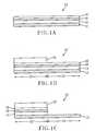
- FIGS. 1A-1Fare pictorial representations (through cross sectional views) illustrating the basic processing steps used in forming a CMOS device containing high performance SOI channel MOSFET semiconductor devices having body contacts.
- FIGS. 2A-2Dare pictorial representations of various wafers that may be bonded together and used in the method described in FIGS. 1A-1F .
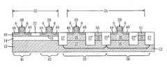
- FIG. 1Aillustrates a substrate 10 , i.e., hybrid substrate, which may be employed in the present invention.
- the substrate 10includes a surface dielectric layer 18 , a first semiconductor layer 16 , an insulating layer 14 , and a second semiconductor layer 12 .
- the surface dielectric layer 18 of the substrate 10is an oxide, nitride, oxynitride or other insulating layer that is either present in one of the initial wafers before bonding, or formed atop the first semiconductor layer 16 after wafer bonding by either a thermal process (i.e., oxidation, nitridation or oxynitridation) or by deposition. Notwithstanding the origin of the surface dielectric layer 18 , the surface dielectric layer 18 has a thickness from about 3 nm to about 500 nm, with a thickness from about 5 nm to about 20 nm being more typical.
- the first semiconductor layer 16is comprised of any semiconducting material including, for example, Si, SiC, SiGe, SiGeC, Ge alloys, GaAs, InAs, InP as well as other III-V or II-VI compound semiconductors.
- First semiconductor layer 16may also comprise an SOI layer of a preformed SOI substrate or a layered semiconductor such as, for example, Si/SiGe.
- the first semiconductor layer 16is a Si-containing semiconducting material.
- the first semiconductor layer 16has the same or different crystalline orientation as the second semiconductor layer 12 , preferably being in the ( 100 ) crystal plane.
- the first semiconductor layer 16may have a ( 111 ) crystal plane, ( 110 ) crystal plane or other crystal plane, so long as the first semiconducting layer 16 is not a Si-containing material that is subsequently processed to provide an NFET device on a ( 110 ) crystal plane.
- the thickness of the first semiconductor layer 16may vary depending on the initial starting wafers used to form the substrate 10 . Typically, however, the first semiconductor layer 16 has an initial thickness from about 5 to about 100 nm, which is then thinned to a thickness of less than 40 nm. The thinning of the first semiconductor layer 16 is performed by planarization, grinding, wet etch, dry etch or any combination thereof. In a preferred embodiment, the first semiconductor layer 16 is thinned by oxidation and wet etching to achieve the desired thickness to provide the upper Si-containing layer of a thin silicon-on-insulator substrate for the purpose of the present invention.
- the insulating layer 14which is located between the first semiconductor layer 16 and the second semiconductor layer 12 has a variable thickness depending upon the initial wafers used to create the substrate 10 . Typically, however, the insulating layer 14 has a thickness from about 1 nm to about 500 nm, with a thickness from about 1 nm to about 100 nm being more typical.
- the insulating layer 14is an oxide or other like insulator material that is formed on one or both of the wafers prior to bonding.
- the second semiconductor layer 12is comprised of any semiconducting material which may be the same or different from that of the first semiconductor layer 16 .
- second semiconductor layer 12may include, for example, Si, SiC, SiGe, SiGeC, Ge alloys, GaAs, InAs, InP as well as other III-V or II-VI compound semiconductors.
- Second semiconductor layer 12may also comprise an SOI layer of a preformed SOI substrate or a layered semiconductor such as, for example, Si/SiGe.
- the second semiconductor layer 12is comprised of a Si-containing semiconducting material.
- the second semiconductor layer 12has the same or differing crystalline orientation as the first semiconductor layer 16 , preferably being in the ( 100 ) crystal plane.
- the second semiconductor layer 12may have a ( 111 ) crystal plane, ( 110 ) crystal plane or other crystal plane, so long as the second semiconducting layer 12 is not a Si-containing material that is subsequently processed to provide an nFET device on a ( 110 ) crystal plane.
- the thickness of the second semiconductor layer 12may vary depending on the initial starting wafers used to form the substrate 10 . Typically, however, the second semiconductor layer 12 has a thickness from about 5 nm to about 200 nm, with a thickness from about 5 to about 100 nm being more typical.
- the substrate 10 illustrated in FIG. 1Ais comprised of two semiconductor wafers that are bonded together.
- the two wafers used in fabricating the substrate 10may include two SOI wafers (See, FIG. 2A ), wherein one of the wafers, designated as 1 , includes the first semiconductor layer 16 and the other wafer, designated as 2 , includes the second semiconductor 12 ; an SOI wafer (designated as 2 ) and a bulk semiconductor wafer (designated as 1 ; See, FIG.
- an SOI waferdesignated as 2
- a bulk waferdesignated as 1
- an ion implant region 11such as a H 2 implant region, which can be used to split a portion of at least one of the wafers during bonding (See FIG. 2C ).
- Bondingis achieved by first bringing the two wafers into intimate contact with other, optionally applying an external force to the contacted wafers, and then heating the two contacted wafers under conditions that are capable of bonding the two wafers together.
- the heating stepmay be performed in the presence or absence of an external force.
- the heating stepis typically performed in an inert ambient at a temperature from about 200° to about 1050° C. for a time period from about 2 to about 20 hours. More typically, the bonding is performed at a temperature from about 200° to about 400° C. for a time period from about 2 to about 20 hours.
- inert ambientis used in the present invention to denote an atmosphere in which an inert gas, such as He, Ar, N 2 , Xe, Kr or a mixture thereof, is employed.
- a preferred ambient used during the bonding processis N 2 .
- some material layers of at least one of the SOI wafersmay be removed after bonding utilizing a planarization process such as chemical mechanical polishing (CMP) or grinding and etching.
- CMPchemical mechanical polishing
- the planarization processstops when surface dielectric layer 18 is reached.
- the ion implant regionforms a porous region during bonding which causes a portion of the wafer above the ion implant region to break off leaving a bonded wafer such as is shown, for example, in FIG. 1A .
- the implant regionis typically comprised of H 2 ions which are implanted into the surface of the wafer utilizing ion implantation conditions that are well known to those skilled in the art.
- the surface dielectric layer 18may be formed atop the bonded wafers by a thermal process, such as oxidation, or by a conventional deposition process, such as chemical vapor deposition (CVD), plasma-enhanced CVD, atomic layer deposition, chemical solution deposition as well as other like deposition processes.
- a thermal processsuch as oxidation
- a conventional deposition processsuch as chemical vapor deposition (CVD), plasma-enhanced CVD, atomic layer deposition, chemical solution deposition as well as other like deposition processes.
- a mask 20is then formed on a predetermined portion of the substrate 10 of FIG. 1A so as to protect a portion of the substrate 10 , while leaving another portion of the substrate 10 unprotected.
- the protected portion of the substrate 10defines a SOI region 22 of the substrate, whereas the unprotected portion of the substrate 10 defines a bulk-Si region 24 .
- the mask 20is formed on a predetermined portion of the surface dielectric layer 18 by applying a photoresist mask to the entire surface of the substrate 10 . After application of the photoresist mask, the mask is patterned by lithography, which includes the steps of exposing the photoresist to a pattern of radiation and developing the pattern utilizing a resist developer.
- the resultant structure including the mask 20 formed on a predetermined portion of the substrate 10is shown, for example, in FIG. 1B .
- the mask 20is a nitride or oxynitride layer that is formed and patterned utilizing lithography and etching.
- the nitride or oxynitride mask 20may be removed after defining the bulk-Si region 24 of the substrate 10 .
- the structureis subjected to one or more etching steps so as to expose a surface of the second semiconductor layer 12 .
- the one or more etching steps used at this point of the present inventionremoves the unprotected portions of the surface dielectric layer 18 , as well as underlying portions of the first semiconductor layer 16 , and a portion of the insulating layer 14 which separates the first semiconductor layer 16 from the second semiconductor layer 12 .
- the etchingmay be performed utilizing a single etching process or multiple etching steps may be employed.
- the etching used at this point of the present inventionmay include a dry etching process such as reactive-ion etching, ion beam etching, plasma etching or laser etching, a wet etching process wherein a chemical etchant is employed or any combination thereof.
- RIEreactive-ion etching
- the resultant structure after the etching process has been performedis shown, for example, in FIG. 1C .
- the sidewalls of the protected SOI region 22i.e., the surface dielectric layer 18 , the first semiconductor layer 16 and the insulating layer 14 , are exposed after this etching step. As shown, the exposed sidewalls of layers 18 , 16 and 14 are aligned with an outer most edge of mask 20 .
- the mask 20is then removed from the structure shown in FIG. 1C utilizing a conventional resist stripping process and then a liner or spacer 25 is typically, but not always, formed on the exposed sidewalls.
- the liner or spacer 25which is optional, is formed by deposition and etching.
- the liner or spacer 25is comprised of an insulating material such as, for example, an oxide.
- a semiconductor material 26is formed on the exposed second semiconductor layer 12 .
- semiconductor material 26has a crystallographic orientation that is the same as the crystallographic orientation of the second semiconductor layer 12 .
- the resultant structureis shown, for example, in FIG. 1D .
- the semiconductor material 26may comprise any Si-containing semiconductor, such as Si, strained Si, SiGe, SiC, SiGeC or combinations thereof, which is capable of being formed utilizing a selective epitaxial growth method.
- semiconductor material 26is comprised of Si.
- semiconductor material 26may be referred to as a regrown semiconductor material 26 .
- the structure shown in FIG. 1Dis subjected to a planarization process such as chemical mechanical polishing (CMP) or grinding such that the upper surface of the semiconductor material 26 is substantially planar with the upper surface of the first semiconductor layer 16 . Note that previously protected portion of surface dielectric layer 18 is removed during this planarization process.
- CMPchemical mechanical polishing
- an isolation region 27such as a shallow trench isolation region, is typically formed so as to isolate the SOI region 22 from the bulk-Si region 24 .
- the isolation region 27is formed utilizing processing steps that are well known to those skilled in the art including, for example, trench definition and etching, optionally lining the trench with a diffusion barrier, and filling the trench with a trench dielectric such as an oxide. After the trench fill, the structure may be planarized and an optional densification processing step may be performed to densify the trench dielectric.
- the resultant substantially planar structure containing isolation region 27is show, for example, in FIG. 1E .
- the structure of FIG. 1Eincludes an exposed first semiconductor layer 16 within the SOI region 22 and the regrown semiconductor material 26 within the bulk-Si region 24 , wherein the first semiconductor layer 16 and the semiconductor material 26 have the same or differing crystal orientation.
- layer 16 and layer 26have the same crystal orientation.
- the SOI region 22is processed to provide SOI MOSFETs and the bulk-Si region 24 is processed to provide devices having body contacts that substantially eliminate floating body effects and provide a means to adjust the threshold voltages of the FETs in the bulk-Si region 24 .
- Device isolation regionsPrior to processing the SOI region 22 and bulk-Si region 24 , device isolation regions may be formed within the substrate 10 .
- Device isolation regions 26can be provided by selectively etching trenches in the substrate utilizing a conventional dry etching process, such as reactive-ion etching (RIE) or plasma etching, in conjunction with conventional block masks.
- RIEreactive-ion etching
- the device isolation regions 26provide isolation within the bulk-Si region 24 and the SOI region 22 and are similar to the isolation region 27 that separates the bulk-Si region 24 from the SOI region 22 .
- the device isolation regions 26may be field isolation regions that are formed using a local oxidation of silicon process.
- the SOI region 22 and the bulk-Si region 24may be individually processed utilizing conventional block mask techniques.
- a block maskmay comprise conventional soft and/or hardmask materials and can be formed using deposition, photolithography and etching.
- the block maskcomprises a photoresist.
- a photoresist block maskcan be produced by applying a blanket photoresist layer to the substrate 10 surface, exposing the photoresist layer to a pattern of radiation, and then developing the pattern into the photoresist layer utilizing a conventional resist developer.
- the block maskcan be a hardmask material.
- Hardmask materialsinclude dielectrics that may be deposited by chemical vapor deposition (CVD) and related methods.
- the hardmask compositionincludes silicon oxides, silicon carbides, silicon nitrides, silicon carbonitrides and other like materials.
- Spin-on dielectricsmay also be utilized as a hardmask material including, but not limited to: silsesquioxanes, siloxanes, and boron phosphate silicate glass (BPSG).
- BPSGboron phosphate silicate glass
- Well regions 37 , 38may be formed in the bulk-Si region 24 by selectively implanting p-type or n-type dopants into the bulk-Si region 24 of the substrate 10 , wherein the SOI region 22 of the substrate 10 may be protected by a block mask, as described above.
- a pFET bulk-Si region 35is implanted to provide an n-type well 37 and an NFET bulk-Si region 36 is implanted to provide a p-type well 38 .
- the SOI layermay also be selectively implanted in the SOI region 22 .
- a pFET SOI region 41is implanted to provide a n-type channel region and an NFET SOI region 42 is implanted to provide a p-type channel region.
- Gate conductor stacks 28 , 29can then be formed within the SOI region 22 and bulk-Si region 24 by first blanket depositing a gate dielectric layer atop the substrate surface and then depositing a gate conductor layer atop the gate dielectric layer.
- the gate dielectric layermay comprise any conventional gate dielectric material, such as SiO 2 , or any high-k gate dielectric material, such as HfO 2 .
- the gate conductor layermay comprise any conductive material, such as doped polysilicon.
- the gate conductor and gate dielectric layerare then etched using conventional deposition, photolithography, and etching to provide gate conductor stacks 28 , 29 within the SOI region 22 and bulk-Si region 24 of the substrate 10 , as depicted in FIG. IF.
- block masksmay be used to provide the gate conductor stacks 28 within the SOI region 22 and the gate conductor stacks 29 within the bulk-Si region 24 separately.
- SOI MOSFET devicesare then selectively formed within the SOI region 22 , while the bulk-Si region 24 is protected by a hard or soft block masks.
- a block mask provided by a patterned photoresistcan be formed prior to implantation to preselect the substrate area within the SOI region 22 for gate conductor and/or source/drain diffusion region 40 doping with one dopant type.
- the block mask application and implantation procedurecan be repeated to dope selected conductive material of gate conductor stacks 28 , source/drain diffusion regions 40 , source/drain extension regions or halo regions (not shown) with different dopant types, such as n-type or p-type dopant.
- the block mask resistmay be removed using conventional photoresist strip chemistries.
- the pattern and implant process stepsmay be repeated to provide at least one pFET device 41 and at least one nFET 42 device, in which the pFET and nFET devices 41 , 42 are separated by isolation regions 26 .
- spacers 6Prior to implantation, spacers 6 are formed abutting the gate conductor stacks 28 , wherein the width of the spacer may be adjusted to compensate for different diffusion rate of the p-type and n-type dopants.
- the pFET and NFET devices within the SOI region 22may be processed to provide silicide regions or any other conventional structures typically utilized in ultra thin channel MOSFETS.
- the hardmaskmay be stripped from the bulk-Si region 24 and another hardmask is then formed atop the SOI region 22 of the substrate 10 leaving the bulk-Si region 24 exposed.
- the bulk-Si region 24can then be processed to provide devices having increased performance on a bulk-Si substrate, as opposed to a SOI substrate.
- the bulk-Si region 24may be processed to provide devices typically common in semiconductor manufacturing, such as resistors; capacitors, including decoupling capacitors, planar capacitors, and deep trench capacitors; diodes; and memory devices, such as dynamic random access memory (DRAM) and embedded dynamic random access memory (eDRAM).
- the bulk-Si region 24comprises body contacts 50 , 51 .
- the bulk-Si region 24is processed to provide MOSFETs having body contacts 50 , 51 .
- the bulk-Si region 24is processed to provide at least one p-type MOSFET 35 and at least one n-type MOSFET 36 each having body contacts 50 , 51 , in which the p-type MOSFETs 35 are separated from the n-type MOSFETs 36 by device isolation regions 26 . Similar to the devices formed within the SOI region 22 , the bulk-Si region 24 may be selectively implanted to provide p-type MOSFETs 35 and n-type MOSFETs 36 utilizing patterned block masks.
- body contacts 50 , 51are then formed to at least one device within the bulk-Si region 24 of the substrate 10 .
- the body contact 50 , 51 to each MOSFET device 35 , 36 within the bulk-Si region 24is in electrical contact to the well region of the device and is separated from the MOSFET's source and drain regions 40 by an isolation region 26 .
- the body contacts 50 , 51may be formed using photolithography, etching, and deposition. More specifically, a body contact 50 , 51 may be formed by patterning a portion of the substrate 10 within the bulk-Si region 24 and etching the exposed surface to form via holes to at least one well region 37 , 36 of at least one MOSFET 35 , 36 .
- the etch processcan be a directional etch, such as reactive-ion etch.
- the body contacts 50 , 51are then formed by depositing a conductive material into the via holes using conventional processing, such as CVD or plating.
- the conductive material used in forming the body contacts 50 , 51may be doped polysilicon or a conductive metal.
- the conductive metalmay include, but is not limited to: tungsten, copper, aluminum, silver, gold, and alloys thereof.
- the body contact 51 to the NFET SOI device 36is p-type doped polysilicon and the body contact 50 to the pFET SOI device 35 is n-type doped polysilicon.
- the devices formed within the SOI region 22 and the devices formed within the bulk-Si region 24 of the substrate 10are both formed atop surfaces having the same crystalline orientation.
- the devices within the SOI region 22 and the devices formed within the bulk-Si region 24are both formed on a surface having a ( 100 ) crystal plane.
- the NFET and pFET devices within the SOI region 22are formed on a surface having a ( 100 ) crystal plane and the pFET devices formed within the bulk-Si region 24 are both formed on a surface having a ( 110 ) crystal plane.
- the pFET devices within the SOI region 22are formed on a surface having a ( 110 ) crystal plane and the NFET and pFET devices formed within the bulk-Si region 24 are both formed on a surface having a ( 100 ) crystal plane.
Landscapes
- Thin Film Transistor (AREA)
- Metal-Oxide And Bipolar Metal-Oxide Semiconductor Integrated Circuits (AREA)
- Element Separation (AREA)
Abstract
Description
- 1. Field of the Invention
- The present invention relates to semiconductor devices, and more particularly to integrated semiconductor devices, such as complementary metal oxide semiconductor (CMOS) devices formed atop a substrate having thin silicon-on-insulator (SOI) and bulk-Si portions, wherein the SOI and bulk-Si portions of the substrate have either the same or different crystalline orientation. In particular, the present invention forms nFET and pFET devices on SOI and bulk-Si regions of a semiconducting substrate having either a surface on a (100), (110), or (111) crystal plane. The bulk-Si region of the substrate is processed to provide devices substantially free of floating body effects that are typically present in the devices formed with SOI substrates. Additionally, in the bulk regions a well contact can be utilized to control the threshold voltage (Vt) of the bulk NFET and pFET devices for improved circuit power and performance.
- 2. Background of the Invention
- Silicon-on-insulator (SOI) devices offer several advantages over more conventional semiconductor devices. For example, SOI devices may have lower power consumption requirements than other types of devices that perform similar tasks. SOI devices may also have lower parasitic capacitances than non-SOI devices. This translates into faster switching times for the resulting circuits. In addition, the phenomenon of “latchup,” which is often exhibited by complementary metal-oxide semiconductor (CMOS) devices, may be avoided when circuit devices are manufactured using SOI fabrication processes. SOI devices are also less susceptible to the adverse effects of ionizing radiation and, therefore, tend to be more reliable in applications where ionizing radiation may cause operation errors.
- Optimization of chip power and performance is becoming increasingly challenging as CMOS technologies are scaled to the 90 nm node and beyond. One technique employed in conventional bulk CMOS is adaptive well biasing. The technique of adaptive well biasing is disclosed, for example, in J. Tschanz, et al., J. Solid State Circuits, 2002, p. 1396. This technique involves varying and selecting optimal biases on the NFET well or body (p-well) node, the pFET well or body (n-well) node, and the power supply (Vdd) node to maximize the power and performance on a per chip basis. In SOI CMOS, this technique is not available as the well nodes (bodies) are floating. In principal, body tie structures may be employed in SOI CMOS to add a contact to the floating body node. The use of body ties structures, however, introduces parasitic resistances and capacitances which would negate the favorable impact of adaptive well biasing.
- A recent innovation, hybrid orientation CMOS technology (HOT) uses both SOI nFETs and pFETs and conventional bulk nFETs and pFETs. HOT technology is described, for example, in M. Yang, et al., IEDM 2003, p.453. and U.S. application Ser. No. 10/250,241, filed Jun. 17, 2003, entitled High-Performance CMOS SOI Devices on Hybrid Crystal Oriented Substrates. Additionally, the same or different crystallographic orientations can be used for NFET and pFET devices. The use of different crystallographic orientations allows for independently optimizing the performance of an nFET (which in silicon has highest mobility and performance in the (100) orientation) and the pFET (which in silicon has the highest mobility and performance in the (110) orientation). Additionally, it is known within the art, that NFET devices formed atop a (110) crystal plane have decreased carrier mobility and switching speed.
- There is thus a need to provide an integrated semiconducting device in which a HOT substrate and adaptive welI biasing are both implemented to provide a structure that has power and performance enhancement.
- The present invention provides a semiconductor structure that includes incoporating field effect transistors (FETs) on a SOI substrate region having a device channel capable of being either partially or fully depleted of charger carriers in combination with FETs within a bulk-Si region having a highly doped well body contact which substantially eliminates floating body effects and provides a means to use adaptive well biasing thereby providing a means to control the threshold voltages of the bulk-Si regions FETs with an applied bias on the well terminal.
- Specifically, the present invention combines a modification of the HOT structure disclosed in M. Yang, et al., IEDM 2003, p.453., whereby a highly doped well is created and contacted for one device type. This provides the means for then applying a bias to implement the adaptive well biasing technique for the device placed in the conventional bulk CMOS region. Additionally, because the well is unipolar, there are no well to well leakage or capacitance penalties for implementing the adaptive well biasing, which is a major advantage over the conventional bulk CMOS scheme for adaptive well biasing.
- Broadly, the present invention provides a semiconducting structure that comprises:
- a substrate comprising an SOI region and a bulk-Si region, wherein said SOI region and said bulk-Si region have a same or differing crystallographic orientation;
- an isolation region separating said SOI region from said bulk-Si region;
- at least one first device located in said SOI region and at least one second device located in said bulk-Si region; and
- a well region underlying said at least one second device and a contact to said well region, wherein said contact stabilizes floating body effects and provides a means for adjusting threshold voltages in field effect transistors (FETs) located in the bulk-Si region through application of a bias voltage.
- In accordance with the present invention, the SOI region of the substrate comprises an SOI layer having a thickness that is capable of being either fully or partially depleted of charge carriers when the device is forward biased. The SOI region may include at least one NFET device, at least one pFET device, or combinations thereof. The bulk-Si region may include at least one nFET, pFET, resistor, capacitor, diode or a combination thereof.
- The above structure can be provided by utilizing a method that includes wafer bonding, masking, etching and regrowth of a semiconductor layer. Specifically, the method of the present invention comprises the steps of providing a substrate comprising at least a first semiconductor layer and a second semiconductor layer separated by an insulating layer, said first semiconductor layer and said second semiconductor layer having a same or differing crystalline orientation; protecting a portion of the substrate to define an SOI region, while leaving another portion of the substrate unprotected, said unprotected portion of the substrate defining a bulk-Si region; etching said unprotected portion of the substrate to expose a surface of the second semiconductor layer; regrowing a semiconductor material on said exposed surface of the second semiconductor layer, said semiconductor material having said same crystalline orientation; planarizing the substrate containing the semiconductor material so that an upper surface of the first semiconductor layer is substantially planar with an upper surface of the semiconductor material; and forming at least one first device in said SOI region, while forming at least one second device on said semiconductor material in said bulk-Si region.
- In accordance with the present invention, the second device within the bulk-Si region can be formed by implanting the bulk-Si region with a first type dopant to provide a well region, forming at least one gate region atop a surface of the bulk-Si region, forming source and drain regions adjacent at least one gate region with a second type dopant, and forming a contact to the well region, wherein the contact stabilizes floating body effects and provides a well contact which may be utilized for adjusting the threshold voltages of the devices in the bulk Si region. Forming the contact to the well region comprises etching a portion of the surface of the bulk-Si region to provide a via to the well region and filling the via to the well region with a conductive material.
FIGS. 1A-1F are pictorial representations (through cross sectional views) illustrating the basic processing steps used in forming a CMOS device containing high performance SOI channel MOSFET semiconductor devices having body contacts.FIGS. 2A-2D are pictorial representations of various wafers that may be bonded together and used in the method described inFIGS. 1A-1F .- The present invention, which provides a hybrid crystal orientation CMOS structure for adaptive well biasing and power/performance enhancement, will now be described in greater detail by referring to the following discussion as well as the drawings that accompany the present application. In the accompanying drawings, like and correspondence elements are referred to by like reference numerals. It is noted that the drawings of the present application are provided for illustrative purposes and thus they are not drawn to scale.
FIG. 1A illustrates asubstrate 10, i.e., hybrid substrate, which may be employed in the present invention. As shown, thesubstrate 10 includes a surfacedielectric layer 18, afirst semiconductor layer 16, aninsulating layer 14, and asecond semiconductor layer 12.- The surface
dielectric layer 18 of thesubstrate 10 is an oxide, nitride, oxynitride or other insulating layer that is either present in one of the initial wafers before bonding, or formed atop thefirst semiconductor layer 16 after wafer bonding by either a thermal process (i.e., oxidation, nitridation or oxynitridation) or by deposition. Notwithstanding the origin of the surfacedielectric layer 18, the surfacedielectric layer 18 has a thickness from about 3 nm to about 500 nm, with a thickness from about 5 nm to about 20 nm being more typical. - The
first semiconductor layer 16 is comprised of any semiconducting material including, for example, Si, SiC, SiGe, SiGeC, Ge alloys, GaAs, InAs, InP as well as other III-V or II-VI compound semiconductors.First semiconductor layer 16 may also comprise an SOI layer of a preformed SOI substrate or a layered semiconductor such as, for example, Si/SiGe. In one preferred embodiment of the present invention, thefirst semiconductor layer 16 is a Si-containing semiconducting material. Thefirst semiconductor layer 16 has the same or different crystalline orientation as thesecond semiconductor layer 12, preferably being in the (100) crystal plane. Although a (100) crystal orientation is preferred, thefirst semiconductor layer 16 may have a (111) crystal plane, (110) crystal plane or other crystal plane, so long as the firstsemiconducting layer 16 is not a Si-containing material that is subsequently processed to provide an NFET device on a (110) crystal plane. - The thickness of the
first semiconductor layer 16 may vary depending on the initial starting wafers used to form thesubstrate 10. Typically, however, thefirst semiconductor layer 16 has an initial thickness from about 5 to about 100 nm, which is then thinned to a thickness of less than 40 nm. The thinning of thefirst semiconductor layer 16 is performed by planarization, grinding, wet etch, dry etch or any combination thereof. In a preferred embodiment, thefirst semiconductor layer 16 is thinned by oxidation and wet etching to achieve the desired thickness to provide the upper Si-containing layer of a thin silicon-on-insulator substrate for the purpose of the present invention. - The insulating
layer 14 which is located between thefirst semiconductor layer 16 and thesecond semiconductor layer 12 has a variable thickness depending upon the initial wafers used to create thesubstrate 10. Typically, however, the insulatinglayer 14 has a thickness from about 1 nm to about 500 nm, with a thickness from about 1 nm to about 100 nm being more typical. The insulatinglayer 14 is an oxide or other like insulator material that is formed on one or both of the wafers prior to bonding. - The
second semiconductor layer 12 is comprised of any semiconducting material which may be the same or different from that of thefirst semiconductor layer 16. Thus,second semiconductor layer 12 may include, for example, Si, SiC, SiGe, SiGeC, Ge alloys, GaAs, InAs, InP as well as other III-V or II-VI compound semiconductors.Second semiconductor layer 12 may also comprise an SOI layer of a preformed SOI substrate or a layered semiconductor such as, for example, Si/SiGe. In a highly preferred embodiment of the present invention, thesecond semiconductor layer 12 is comprised of a Si-containing semiconducting material. Thesecond semiconductor layer 12 has the same or differing crystalline orientation as thefirst semiconductor layer 16, preferably being in the (100) crystal plane. Although a (100) crystal orientation is preferred, thesecond semiconductor layer 12 may have a (111) crystal plane, (110) crystal plane or other crystal plane, so long as the secondsemiconducting layer 12 is not a Si-containing material that is subsequently processed to provide an nFET device on a (110) crystal plane. - The thickness of the
second semiconductor layer 12 may vary depending on the initial starting wafers used to form thesubstrate 10. Typically, however, thesecond semiconductor layer 12 has a thickness from about 5 nm to about 200 nm, with a thickness from about 5 to about 100 nm being more typical. - The
substrate 10 illustrated inFIG. 1A is comprised of two semiconductor wafers that are bonded together. The two wafers used in fabricating thesubstrate 10 may include two SOI wafers (See,FIG. 2A ), wherein one of the wafers, designated as1, includes thefirst semiconductor layer 16 and the other wafer, designated as2, includes thesecond semiconductor 12; an SOI wafer (designated as2) and a bulk semiconductor wafer (designated as1; See,FIG. 2B ); or an SOI wafer (designated as2) and a bulk wafer (designated as1) which includes anion implant region 11, such as a H2implant region, which can be used to split a portion of at least one of the wafers during bonding (SeeFIG. 2C ). - Bonding is achieved by first bringing the two wafers into intimate contact with other, optionally applying an external force to the contacted wafers, and then heating the two contacted wafers under conditions that are capable of bonding the two wafers together. The heating step may be performed in the presence or absence of an external force. The heating step is typically performed in an inert ambient at a temperature from about 200° to about 1050° C. for a time period from about 2 to about 20 hours. More typically, the bonding is performed at a temperature from about 200° to about 400° C. for a time period from about 2 to about 20 hours. The term “inert ambient” is used in the present invention to denote an atmosphere in which an inert gas, such as He, Ar, N2, Xe, Kr or a mixture thereof, is employed. A preferred ambient used during the bonding process is N2.
- In the embodiment where two SOI wafers are employed, some material layers of at least one of the SOI wafers may be removed after bonding utilizing a planarization process such as chemical mechanical polishing (CMP) or grinding and etching. The planarization process stops when
surface dielectric layer 18 is reached. - In the embodiment in which one of the wafers includes an ion implant region, the ion implant region forms a porous region during bonding which causes a portion of the wafer above the ion implant region to break off leaving a bonded wafer such as is shown, for example, in
FIG. 1A . The implant region is typically comprised of H2ions which are implanted into the surface of the wafer utilizing ion implantation conditions that are well known to those skilled in the art. - In the embodiment where the wafers to be bonded do not include a dielectric layer therein, the
surface dielectric layer 18 may be formed atop the bonded wafers by a thermal process, such as oxidation, or by a conventional deposition process, such as chemical vapor deposition (CVD), plasma-enhanced CVD, atomic layer deposition, chemical solution deposition as well as other like deposition processes. - Referring now to
FIG. 1B , amask 20 is then formed on a predetermined portion of thesubstrate 10 ofFIG. 1A so as to protect a portion of thesubstrate 10, while leaving another portion of thesubstrate 10 unprotected. The protected portion of thesubstrate 10 defines aSOI region 22 of the substrate, whereas the unprotected portion of thesubstrate 10 defines a bulk-Si region 24. In one embodiment, themask 20 is formed on a predetermined portion of thesurface dielectric layer 18 by applying a photoresist mask to the entire surface of thesubstrate 10. After application of the photoresist mask, the mask is patterned by lithography, which includes the steps of exposing the photoresist to a pattern of radiation and developing the pattern utilizing a resist developer. The resultant structure including themask 20 formed on a predetermined portion of thesubstrate 10 is shown, for example, inFIG. 1B . - In another embodiment, the
mask 20 is a nitride or oxynitride layer that is formed and patterned utilizing lithography and etching. The nitride oroxynitride mask 20 may be removed after defining the bulk-Si region 24 of thesubstrate 10. - After forming the
mask 20 atop thesubstrate 10, the structure is subjected to one or more etching steps so as to expose a surface of thesecond semiconductor layer 12. Specifically, the one or more etching steps used at this point of the present invention removes the unprotected portions of thesurface dielectric layer 18, as well as underlying portions of thefirst semiconductor layer 16, and a portion of the insulatinglayer 14 which separates thefirst semiconductor layer 16 from thesecond semiconductor layer 12. The etching may be performed utilizing a single etching process or multiple etching steps may be employed. The etching used at this point of the present invention may include a dry etching process such as reactive-ion etching, ion beam etching, plasma etching or laser etching, a wet etching process wherein a chemical etchant is employed or any combination thereof. In a preferred embodiment of the present invention, reactive-ion etching (RIE) is used in selectively removing the unprotected portions of thesurface dielectric layer 18, thefirst semiconductor layer 16 and the insulatinglayer 14 in the bulk-Si region 24. The resultant structure after the etching process has been performed is shown, for example, inFIG. 1C . Note that the sidewalls of the protectedSOI region 22, i.e., thesurface dielectric layer 18, thefirst semiconductor layer 16 and the insulatinglayer 14, are exposed after this etching step. As shown, the exposed sidewalls oflayers mask 20. - The
mask 20 is then removed from the structure shown inFIG. 1C utilizing a conventional resist stripping process and then a liner orspacer 25 is typically, but not always, formed on the exposed sidewalls. The liner orspacer 25, which is optional, is formed by deposition and etching. The liner orspacer 25 is comprised of an insulating material such as, for example, an oxide. - After forming the optional liner or
spacer 25, asemiconductor material 26 is formed on the exposedsecond semiconductor layer 12. In accordance with the present invention,semiconductor material 26 has a crystallographic orientation that is the same as the crystallographic orientation of thesecond semiconductor layer 12. The resultant structure is shown, for example, inFIG. 1D . - The
semiconductor material 26 may comprise any Si-containing semiconductor, such as Si, strained Si, SiGe, SiC, SiGeC or combinations thereof, which is capable of being formed utilizing a selective epitaxial growth method. In some preferred embodiments,semiconductor material 26 is comprised of Si. In the present invention,semiconductor material 26 may be referred to as aregrown semiconductor material 26. - Next, the structure shown in
FIG. 1D is subjected to a planarization process such as chemical mechanical polishing (CMP) or grinding such that the upper surface of thesemiconductor material 26 is substantially planar with the upper surface of thefirst semiconductor layer 16. Note that previously protected portion ofsurface dielectric layer 18 is removed during this planarization process. - After providing the substantially planar surfaces, an
isolation region 27, such as a shallow trench isolation region, is typically formed so as to isolate theSOI region 22 from the bulk-Si region 24. Theisolation region 27 is formed utilizing processing steps that are well known to those skilled in the art including, for example, trench definition and etching, optionally lining the trench with a diffusion barrier, and filling the trench with a trench dielectric such as an oxide. After the trench fill, the structure may be planarized and an optional densification processing step may be performed to densify the trench dielectric. - The resultant substantially planar structure containing
isolation region 27 is show, for example, inFIG. 1E . As shown, the structure ofFIG. 1E includes an exposedfirst semiconductor layer 16 within theSOI region 22 and theregrown semiconductor material 26 within the bulk-Si region 24, wherein thefirst semiconductor layer 16 and thesemiconductor material 26 have the same or differing crystal orientation. In one preffered embodiment,layer 16 andlayer 26 have the same crystal orientation. In that embodiment, it is highly preferably that layers16 and26 have a surface in the (100) crystal plane. - Referring to
FIG. 1F , in a next process step, theSOI region 22 is processed to provide SOI MOSFETs and the bulk-Si region 24 is processed to provide devices having body contacts that substantially eliminate floating body effects and provide a means to adjust the threshold voltages of the FETs in the bulk-Si region 24. - Prior to processing the
SOI region 22 and bulk-Si region 24, device isolation regions may be formed within thesubstrate 10.Device isolation regions 26 can be provided by selectively etching trenches in the substrate utilizing a conventional dry etching process, such as reactive-ion etching (RIE) or plasma etching, in conjunction with conventional block masks. Thedevice isolation regions 26 provide isolation within the bulk-Si region 24 and theSOI region 22 and are similar to theisolation region 27 that separates the bulk-Si region 24 from theSOI region 22. Alternatively, thedevice isolation regions 26 may be field isolation regions that are formed using a local oxidation of silicon process. - The
SOI region 22 and the bulk-Si region 24 may be individually processed utilizing conventional block mask techniques. A block mask may comprise conventional soft and/or hardmask materials and can be formed using deposition, photolithography and etching. In a preferred embodiment, the block mask comprises a photoresist. A photoresist block mask can be produced by applying a blanket photoresist layer to thesubstrate 10 surface, exposing the photoresist layer to a pattern of radiation, and then developing the pattern into the photoresist layer utilizing a conventional resist developer. - Alternatively, the block mask can be a hardmask material. Hardmask materials include dielectrics that may be deposited by chemical vapor deposition (CVD) and related methods. Typically, the hardmask composition includes silicon oxides, silicon carbides, silicon nitrides, silicon carbonitrides and other like materials. Spin-on dielectrics may also be utilized as a hardmask material including, but not limited to: silsesquioxanes, siloxanes, and boron phosphate silicate glass (BPSG).
Well regions Si region 24 by selectively implanting p-type or n-type dopants into the bulk-Si region 24 of thesubstrate 10, wherein theSOI region 22 of thesubstrate 10 may be protected by a block mask, as described above. In the example depicted inFIG. 1F , a pFET bulk-Si region 35 is implanted to provide an n-type well 37 and an NFET bulk-Si region 36 is implanted to provide a p-type well 38.- The SOI layer may also be selectively implanted in the
SOI region 22. In the example depicted byFIG. 1F , apFET SOI region 41 is implanted to provide a n-type channel region and anNFET SOI region 42 is implanted to provide a p-type channel region. - Gate conductor stacks28,29 can then be formed within the
SOI region 22 and bulk-Si region 24 by first blanket depositing a gate dielectric layer atop the substrate surface and then depositing a gate conductor layer atop the gate dielectric layer. The gate dielectric layer may comprise any conventional gate dielectric material, such as SiO2, or any high-k gate dielectric material, such as HfO2. The gate conductor layer may comprise any conductive material, such as doped polysilicon. The gate conductor and gate dielectric layer are then etched using conventional deposition, photolithography, and etching to provide gate conductor stacks28,29 within theSOI region 22 and bulk-Si region 24 of thesubstrate 10, as depicted in FIG. IF. Alternatively, block masks may be used to provide the gate conductor stacks28 within theSOI region 22 and the gate conductor stacks29 within the bulk-Si region 24 separately. - In the embodiment depicted in
FIG. 1F and during a next series of process steps, SOI MOSFET devices are then selectively formed within theSOI region 22, while the bulk-Si region 24 is protected by a hard or soft block masks. For example, a block mask provided by a patterned photoresist can be formed prior to implantation to preselect the substrate area within theSOI region 22 for gate conductor and/or source/drain diffusion region 40 doping with one dopant type. The block mask application and implantation procedure can be repeated to dope selected conductive material of gate conductor stacks28, source/drain diffusion regions 40, source/drain extension regions or halo regions (not shown) with different dopant types, such as n-type or p-type dopant. After each implant, the block mask resist may be removed using conventional photoresist strip chemistries. In one preferred embodiment, the pattern and implant process steps may be repeated to provide at least onepFET device 41 and at least one nFET42 device, in which the pFET andnFET devices isolation regions 26. - Prior to implantation,
spacers 6 are formed abutting the gate conductor stacks28, wherein the width of the spacer may be adjusted to compensate for different diffusion rate of the p-type and n-type dopants. In addition, the pFET and NFET devices within theSOI region 22 may be processed to provide silicide regions or any other conventional structures typically utilized in ultra thin channel MOSFETS. Following the formation of thedevices SOI region 22, the hardmask may be stripped from the bulk-Si region 24 and another hardmask is then formed atop theSOI region 22 of thesubstrate 10 leaving the bulk-Si region 24 exposed. - The bulk-
Si region 24 can then be processed to provide devices having increased performance on a bulk-Si substrate, as opposed to a SOI substrate. For example, the bulk-Si region 24 may be processed to provide devices typically common in semiconductor manufacturing, such as resistors; capacitors, including decoupling capacitors, planar capacitors, and deep trench capacitors; diodes; and memory devices, such as dynamic random access memory (DRAM) and embedded dynamic random access memory (eDRAM). In a preferred embodiment, the bulk-Si region 24 comprisesbody contacts FIG. 1F , the bulk-Si region 24 is processed to provide MOSFETs havingbody contacts - In the embodiment depicted in
FIG. 1F , the bulk-Si region 24 is processed to provide at least one p-type MOSFET 35 and at least one n-type MOSFET 36 each havingbody contacts type MOSFETs 35 are separated from the n-type MOSFETs 36 bydevice isolation regions 26. Similar to the devices formed within theSOI region 22, the bulk-Si region 24 may be selectively implanted to provide p-type MOSFETs 35 and n-type MOSFETs 36 utilizing patterned block masks. - Following implantation,
body contacts Si region 24 of thesubstrate 10. Thebody contact MOSFET device Si region 24 is in electrical contact to the well region of the device and is separated from the MOSFET's source and drainregions 40 by anisolation region 26. - The
body contacts body contact substrate 10 within the bulk-Si region 24 and etching the exposed surface to form via holes to at least onewell region MOSFET body contacts body contacts body contact 51 to theNFET SOI device 36 is p-type doped polysilicon and thebody contact 50 to thepFET SOI device 35 is n-type doped polysilicon. - Note that the devices formed within the
SOI region 22 and the devices formed within the bulk-Si region 24 of thesubstrate 10 are both formed atop surfaces having the same crystalline orientation. In one preferred embodiment, the devices within theSOI region 22 and the devices formed within the bulk-Si region 24 are both formed on a surface having a (100) crystal plane. In another preferred embodiment, the NFET and pFET devices within theSOI region 22 are formed on a surface having a (100) crystal plane and the pFET devices formed within the bulk-Si region 24 are both formed on a surface having a (110) crystal plane. In another preferred embodiment, the pFET devices within theSOI region 22 are formed on a surface having a (110) crystal plane and the NFET and pFET devices formed within the bulk-Si region 24 are both formed on a surface having a (100) crystal plane. - While the present invention has been particularly shown and described with respect to preferred embodiments thereof, it will be understood by those skilled in the art that the foregoing and other changes in forms and details may be made without departing from the spirit and scope of the present invention. It is therefore intended that the present invention not be limited to the exact forms and details described and illustrated, but fall within the scope of the appended claims
Claims (25)
Priority Applications (7)
| Application Number | Priority Date | Filing Date | Title |
|---|---|---|---|
| US11/107,611US7605429B2 (en) | 2005-04-15 | 2005-04-15 | Hybrid crystal orientation CMOS structure for adaptive well biasing and for power and performance enhancement |
| PCT/US2006/011558WO2006113077A2 (en) | 2005-04-15 | 2006-03-30 | Hybrid crystal orientation cmos structure for adaptive well biasing and for power and performance enhancement |
| JP2008506492AJP2008536335A (en) | 2005-04-15 | 2006-03-30 | Hybrid crystal-oriented CMOS structure for adaptive well biasing and power and performance enhancement |
| CNB2006800093334ACN100524783C (en) | 2005-04-15 | 2006-03-30 | Semiconductor structure and manufacturing method thereof |
| EP06740000AEP1875507A4 (en) | 2005-04-15 | 2006-03-30 | HYBRID CRYSTALLINE ORIENTATION CMOS STRUCTURE FOR ADAPTIVE WELL POLARIZATION AND IMPROVING POWER AND PERFORMANCE |
| TW095112247ATW200636909A (en) | 2005-04-15 | 2006-04-06 | Hybrid crystal orientation CMOS structure for adaptive well biasing and for power and performance enhancement |
| US11/859,889US7629233B2 (en) | 2005-04-15 | 2007-09-24 | Hybrid crystal orientation CMOS structure for adaptive well biasing and for power and performance enhancement |
Applications Claiming Priority (1)
| Application Number | Priority Date | Filing Date | Title |
|---|---|---|---|
| US11/107,611US7605429B2 (en) | 2005-04-15 | 2005-04-15 | Hybrid crystal orientation CMOS structure for adaptive well biasing and for power and performance enhancement |
Related Child Applications (1)
| Application Number | Title | Priority Date | Filing Date |
|---|---|---|---|
| US11/859,889DivisionUS7629233B2 (en) | 2005-04-15 | 2007-09-24 | Hybrid crystal orientation CMOS structure for adaptive well biasing and for power and performance enhancement |
Publications (2)
| Publication Number | Publication Date |
|---|---|
| US20060231893A1true US20060231893A1 (en) | 2006-10-19 |
| US7605429B2 US7605429B2 (en) | 2009-10-20 |
Family
ID=37107693
Family Applications (2)
| Application Number | Title | Priority Date | Filing Date |
|---|---|---|---|
| US11/107,611Active2025-10-20US7605429B2 (en) | 2005-04-15 | 2005-04-15 | Hybrid crystal orientation CMOS structure for adaptive well biasing and for power and performance enhancement |
| US11/859,889Expired - Fee RelatedUS7629233B2 (en) | 2005-04-15 | 2007-09-24 | Hybrid crystal orientation CMOS structure for adaptive well biasing and for power and performance enhancement |
Family Applications After (1)
| Application Number | Title | Priority Date | Filing Date |
|---|---|---|---|
| US11/859,889Expired - Fee RelatedUS7629233B2 (en) | 2005-04-15 | 2007-09-24 | Hybrid crystal orientation CMOS structure for adaptive well biasing and for power and performance enhancement |
Country Status (6)
| Country | Link |
|---|---|
| US (2) | US7605429B2 (en) |
| EP (1) | EP1875507A4 (en) |
| JP (1) | JP2008536335A (en) |
| CN (1) | CN100524783C (en) |
| TW (1) | TW200636909A (en) |
| WO (1) | WO2006113077A2 (en) |
Cited By (19)
| Publication number | Priority date | Publication date | Assignee | Title |
|---|---|---|---|---|
| US20060284251A1 (en)* | 2005-06-16 | 2006-12-21 | International Business Machines Corporation | Coplanar silicon-on-insulator (SOI) regions of different crystal orientations and methods of making the same |
| US20060286781A1 (en)* | 2005-06-16 | 2006-12-21 | International Business Machines Corporation | Crystal imprinting methods for fabricating subsrates with thin active silicon layers |
| US20060284250A1 (en)* | 2005-06-16 | 2006-12-21 | International Business Machines Corporation | Hybrid oriented substrates and crystal imprinting methods for forming such hybrid oriented substrates |
| US20070194383A1 (en)* | 2006-02-23 | 2007-08-23 | Seiko Epson Corporation | Semiconductor device |
| US20070215943A1 (en)* | 2006-03-17 | 2007-09-20 | Kabushiki Kaisha Toshiba | Semiconductor device and method for manufacturing the same |
| US20080258222A1 (en)* | 2007-04-20 | 2008-10-23 | International Business Machines Corporation | Design Structure Incorporating a Hybrid Substrate |
| US20080258181A1 (en)* | 2007-04-20 | 2008-10-23 | Ethan Harrison Cannon | Hybrid Substrates and Methods for Forming Such Hybrid Substrates |
| US20090108292A1 (en)* | 2007-10-26 | 2009-04-30 | Jun Liu | Floating Body Field-Effect Transistors, and Methods of Forming Floating Body Field-Effect Transistors |
| KR100934849B1 (en)* | 2008-01-07 | 2009-12-31 | 주식회사 하이닉스반도체 | Semiconductor device formation method |
| US20110108943A1 (en)* | 2009-11-06 | 2011-05-12 | International Business Machines Corporation | Hybrid double box back gate silicon-on-insulator wafers with enhanced mobility channels |
| US20110163380A1 (en)* | 2010-01-07 | 2011-07-07 | International Business Machines Corporation | Body-Tied Asymmetric N-Type Field Effect Transistor |
| US20110163379A1 (en)* | 2010-01-07 | 2011-07-07 | International Business Machines Corporation | Body-Tied Asymmetric P-Type Field Effect Transistor |
| CN102468332A (en)* | 2010-11-03 | 2012-05-23 | 中国科学院微电子研究所 | A MOS transistor based on silicon-on-insulator |
| US20120313172A1 (en)* | 2011-06-07 | 2012-12-13 | Renesas Electronics Corporation | Semiconductor device, semiconductor wafer, and methods of manufacturing the same |
| US8704286B2 (en) | 2008-12-18 | 2014-04-22 | Micron Technology, Inc. | Method and structure for integrating capacitor-less memory cell with logic |
| US8877606B2 (en) | 2009-01-12 | 2014-11-04 | International Business Machines Corporation | Low cost fabrication of double box back gate silicon-on-insulator wafers with subsequent self aligned shallow trench isolation |
| US10109638B1 (en)* | 2017-10-23 | 2018-10-23 | Globalfoundries Singapore Pte. Ltd. | Embedded non-volatile memory (NVM) on fully depleted silicon-on-insulator (FD-SOI) substrate |
| US11335674B2 (en)* | 2019-06-27 | 2022-05-17 | Globalfoundries U.S. Inc. | Diode triggered silicon controlled rectifier (SCR) with hybrid diodes |
| US11430881B2 (en) | 2020-03-05 | 2022-08-30 | Globalfoundries U.S. Inc. | Diode triggered compact silicon controlled rectifier |
Families Citing this family (74)
| Publication number | Priority date | Publication date | Assignee | Title |
|---|---|---|---|---|
| US7087965B2 (en)* | 2004-04-22 | 2006-08-08 | International Business Machines Corporation | Strained silicon CMOS on hybrid crystal orientations |
| US8866190B2 (en)* | 2005-06-14 | 2014-10-21 | International Rectifler Corporation | Methods of combining silicon and III-nitride material on a single wafer |
| DE102006015076B4 (en)* | 2006-03-31 | 2014-03-20 | Advanced Micro Devices, Inc. | Semiconductor device with SOI transistors and solid-state transistors and a method for manufacturing |
| US7285480B1 (en)* | 2006-04-07 | 2007-10-23 | International Business Machines Corporation | Integrated circuit chip with FETs having mixed body thicknesses and method of manufacture thereof |
| US7718496B2 (en)* | 2007-10-30 | 2010-05-18 | International Business Machines Corporation | Techniques for enabling multiple Vt devices using high-K metal gate stacks |
| US8278731B2 (en)* | 2007-11-20 | 2012-10-02 | Denso Corporation | Semiconductor device having SOI substrate and method for manufacturing the same |
| US7847353B2 (en)* | 2008-12-05 | 2010-12-07 | Bae Systems Information And Electronic Systems Integration Inc. | Multi-thickness semiconductor with fully depleted devices and photonic integration |
| US8421162B2 (en) | 2009-09-30 | 2013-04-16 | Suvolta, Inc. | Advanced transistors with punch through suppression |
| US8273617B2 (en) | 2009-09-30 | 2012-09-25 | Suvolta, Inc. | Electronic devices and systems, and methods for making and using the same |
| WO2011062788A1 (en)* | 2009-11-17 | 2011-05-26 | Suvolta, Inc. | Electronic devices and systems, and methods for making and using the same |
| US8530286B2 (en) | 2010-04-12 | 2013-09-10 | Suvolta, Inc. | Low power semiconductor transistor structure and method of fabrication thereof |
| US8569128B2 (en) | 2010-06-21 | 2013-10-29 | Suvolta, Inc. | Semiconductor structure and method of fabrication thereof with mixed metal types |
| US8759872B2 (en) | 2010-06-22 | 2014-06-24 | Suvolta, Inc. | Transistor with threshold voltage set notch and method of fabrication thereof |
| US8377783B2 (en) | 2010-09-30 | 2013-02-19 | Suvolta, Inc. | Method for reducing punch-through in a transistor device |
| US8404551B2 (en) | 2010-12-03 | 2013-03-26 | Suvolta, Inc. | Source/drain extension control for advanced transistors |
| US8461875B1 (en) | 2011-02-18 | 2013-06-11 | Suvolta, Inc. | Digital circuits having improved transistors, and methods therefor |
| US8525271B2 (en) | 2011-03-03 | 2013-09-03 | Suvolta, Inc. | Semiconductor structure with improved channel stack and method for fabrication thereof |
| US8400219B2 (en) | 2011-03-24 | 2013-03-19 | Suvolta, Inc. | Analog circuits having improved transistors, and methods therefor |
| US8748270B1 (en) | 2011-03-30 | 2014-06-10 | Suvolta, Inc. | Process for manufacturing an improved analog transistor |
| US8492207B2 (en) | 2011-04-21 | 2013-07-23 | International Business Machines Corporation | Implementing eFuse circuit with enhanced eFuse blow operation |
| US8525245B2 (en) | 2011-04-21 | 2013-09-03 | International Business Machines Corporation | eDRAM having dynamic retention and performance tradeoff |
| US8456187B2 (en) | 2011-04-21 | 2013-06-04 | International Business Machines Corporation | Implementing temporary disable function of protected circuitry by modulating threshold voltage of timing sensitive circuit |
| US8816470B2 (en) | 2011-04-21 | 2014-08-26 | International Business Machines Corporation | Independently voltage controlled volume of silicon on a silicon on insulator chip |
| US8796048B1 (en) | 2011-05-11 | 2014-08-05 | Suvolta, Inc. | Monitoring and measurement of thin film layers |
| US8999861B1 (en) | 2011-05-11 | 2015-04-07 | Suvolta, Inc. | Semiconductor structure with substitutional boron and method for fabrication thereof |
| US8811068B1 (en) | 2011-05-13 | 2014-08-19 | Suvolta, Inc. | Integrated circuit devices and methods |
| US8569156B1 (en) | 2011-05-16 | 2013-10-29 | Suvolta, Inc. | Reducing or eliminating pre-amorphization in transistor manufacture |
| US8735987B1 (en) | 2011-06-06 | 2014-05-27 | Suvolta, Inc. | CMOS gate stack structures and processes |
| US8995204B2 (en) | 2011-06-23 | 2015-03-31 | Suvolta, Inc. | Circuit devices and methods having adjustable transistor body bias |
| US8416009B2 (en) | 2011-07-13 | 2013-04-09 | International Business Machines Corporation | Solutions for controlling bulk bias voltage in an extremely thin silicon-on-insulator (ETSOI) integrated circuit chip |
| US8629016B1 (en) | 2011-07-26 | 2014-01-14 | Suvolta, Inc. | Multiple transistor types formed in a common epitaxial layer by differential out-diffusion from a doped underlayer |
| KR101891373B1 (en) | 2011-08-05 | 2018-08-24 | 엠아이이 후지쯔 세미컨덕터 리미티드 | Semiconductor devices having fin structures and fabrication methods thereof |
| US8748986B1 (en) | 2011-08-05 | 2014-06-10 | Suvolta, Inc. | Electronic device with controlled threshold voltage |
| US8614128B1 (en) | 2011-08-23 | 2013-12-24 | Suvolta, Inc. | CMOS structures and processes based on selective thinning |
| US8645878B1 (en) | 2011-08-23 | 2014-02-04 | Suvolta, Inc. | Porting a circuit design from a first semiconductor process to a second semiconductor process |
| US8713511B1 (en) | 2011-09-16 | 2014-04-29 | Suvolta, Inc. | Tools and methods for yield-aware semiconductor manufacturing process target generation |
| US9236466B1 (en) | 2011-10-07 | 2016-01-12 | Mie Fujitsu Semiconductor Limited | Analog circuits having improved insulated gate transistors, and methods therefor |
| US8895327B1 (en) | 2011-12-09 | 2014-11-25 | Suvolta, Inc. | Tipless transistors, short-tip transistors, and methods and circuits therefor |
| US8819603B1 (en) | 2011-12-15 | 2014-08-26 | Suvolta, Inc. | Memory circuits and methods of making and designing the same |
| US8883600B1 (en) | 2011-12-22 | 2014-11-11 | Suvolta, Inc. | Transistor having reduced junction leakage and methods of forming thereof |
| US8599623B1 (en) | 2011-12-23 | 2013-12-03 | Suvolta, Inc. | Circuits and methods for measuring circuit elements in an integrated circuit device |
| US8970289B1 (en) | 2012-01-23 | 2015-03-03 | Suvolta, Inc. | Circuits and devices for generating bi-directional body bias voltages, and methods therefor |
| US8877619B1 (en) | 2012-01-23 | 2014-11-04 | Suvolta, Inc. | Process for manufacture of integrated circuits with different channel doping transistor architectures and devices therefrom |
| US9093550B1 (en) | 2012-01-31 | 2015-07-28 | Mie Fujitsu Semiconductor Limited | Integrated circuits having a plurality of high-K metal gate FETs with various combinations of channel foundation structure and gate stack structure and methods of making same |
| US9406567B1 (en) | 2012-02-28 | 2016-08-02 | Mie Fujitsu Semiconductor Limited | Method for fabricating multiple transistor devices on a substrate with varying threshold voltages |
| US8863064B1 (en) | 2012-03-23 | 2014-10-14 | Suvolta, Inc. | SRAM cell layout structure and devices therefrom |
| JP2013232471A (en)* | 2012-04-27 | 2013-11-14 | National Institute Of Advanced Industrial & Technology | Complementary semiconductor device and method of manufacturing the same |
| CN103515317B (en)* | 2012-06-20 | 2016-02-03 | 中芯国际集成电路制造(上海)有限公司 | A kind of cmos device and forming method thereof |
| US9299698B2 (en) | 2012-06-27 | 2016-03-29 | Mie Fujitsu Semiconductor Limited | Semiconductor structure with multiple transistors having various threshold voltages |
| CN102738179B (en)* | 2012-07-16 | 2015-08-19 | 西安电子科技大学 | A kind of SOI strain SiGe CMOS integrated device and preparation method |
| US8637955B1 (en) | 2012-08-31 | 2014-01-28 | Suvolta, Inc. | Semiconductor structure with reduced junction leakage and method of fabrication thereof |
| US9112057B1 (en) | 2012-09-18 | 2015-08-18 | Mie Fujitsu Semiconductor Limited | Semiconductor devices with dopant migration suppression and method of fabrication thereof |
| US9041126B2 (en) | 2012-09-21 | 2015-05-26 | Mie Fujitsu Semiconductor Limited | Deeply depleted MOS transistors having a screening layer and methods thereof |
| US9431068B2 (en) | 2012-10-31 | 2016-08-30 | Mie Fujitsu Semiconductor Limited | Dynamic random access memory (DRAM) with low variation transistor peripheral circuits |
| US8816754B1 (en) | 2012-11-02 | 2014-08-26 | Suvolta, Inc. | Body bias circuits and methods |
| US9093997B1 (en) | 2012-11-15 | 2015-07-28 | Mie Fujitsu Semiconductor Limited | Slew based process and bias monitors and related methods |
| US9070477B1 (en) | 2012-12-12 | 2015-06-30 | Mie Fujitsu Semiconductor Limited | Bit interleaved low voltage static random access memory (SRAM) and related methods |
| US9112484B1 (en) | 2012-12-20 | 2015-08-18 | Mie Fujitsu Semiconductor Limited | Integrated circuit process and bias monitors and related methods |
| US9268885B1 (en) | 2013-02-28 | 2016-02-23 | Mie Fujitsu Semiconductor Limited | Integrated circuit device methods and models with predicted device metric variations |
| US8994415B1 (en) | 2013-03-01 | 2015-03-31 | Suvolta, Inc. | Multiple VDD clock buffer |
| US8988153B1 (en) | 2013-03-09 | 2015-03-24 | Suvolta, Inc. | Ring oscillator with NMOS or PMOS variation insensitivity |
| US9299801B1 (en) | 2013-03-14 | 2016-03-29 | Mie Fujitsu Semiconductor Limited | Method for fabricating a transistor device with a tuned dopant profile |
| US9449967B1 (en) | 2013-03-15 | 2016-09-20 | Fujitsu Semiconductor Limited | Transistor array structure |
| US9112495B1 (en) | 2013-03-15 | 2015-08-18 | Mie Fujitsu Semiconductor Limited | Integrated circuit device body bias circuits and methods |
| US9478571B1 (en) | 2013-05-24 | 2016-10-25 | Mie Fujitsu Semiconductor Limited | Buried channel deeply depleted channel transistor |
| US8976575B1 (en) | 2013-08-29 | 2015-03-10 | Suvolta, Inc. | SRAM performance monitor |
| US9490161B2 (en) | 2014-04-29 | 2016-11-08 | International Business Machines Corporation | Channel SiGe devices with multiple threshold voltages on hybrid oriented substrates, and methods of manufacturing same |
| US9324632B2 (en) | 2014-05-28 | 2016-04-26 | Globalfoundries Inc. | Semiconductor structures with isolated ohmic trenches and stand-alone isolation trenches and related method |
| US9710006B2 (en) | 2014-07-25 | 2017-07-18 | Mie Fujitsu Semiconductor Limited | Power up body bias circuits and methods |
| US9319013B2 (en) | 2014-08-19 | 2016-04-19 | Mie Fujitsu Semiconductor Limited | Operational amplifier input offset correction with transistor threshold voltage adjustment |
| US10438792B2 (en)* | 2016-10-20 | 2019-10-08 | QROMIS, Inc. | Methods for integration of elemental and compound semiconductors on a ceramic substrate |
| US10727244B2 (en) | 2017-06-12 | 2020-07-28 | Samsung Electronics Co., Ltd. | Semiconductor memory devices and methods of fabricating the same |
| US10403634B2 (en) | 2017-06-12 | 2019-09-03 | Samsung Electronics Co., Ltd | Semiconductor memory device and method of manufacturing the same |
| SG10201803464XA (en) | 2017-06-12 | 2019-01-30 | Samsung Electronics Co Ltd | Semiconductor memory device and method of manufacturing the same |
Citations (13)
| Publication number | Priority date | Publication date | Assignee | Title |
|---|---|---|---|---|
| US4927678A (en)* | 1987-12-01 | 1990-05-22 | Compagnie Des Products Industriels de l'Ouest (C.P.I.O.) | Protective bellows particularly for a motor vehicle front wheel drive |
| US5240766A (en)* | 1992-04-01 | 1993-08-31 | Hollingsworth & Vose Company | Gasket material |
| US5384473A (en)* | 1991-10-01 | 1995-01-24 | Kabushiki Kaisha Toshiba | Semiconductor body having element formation surfaces with different orientations |
| US5707066A (en)* | 1994-12-02 | 1998-01-13 | Nok Corporation | Boot assembly with adapter |
| US5985708A (en)* | 1996-03-13 | 1999-11-16 | Kabushiki Kaisha Toshiba | Method of manufacturing vertical power device |
| US6337253B1 (en)* | 1999-01-14 | 2002-01-08 | International Business Machines Corporation | Process of making buried capacitor for silicon-on-insulator structure |
| US20020115244A1 (en)* | 2000-08-11 | 2002-08-22 | Sung-Bae Park | SOI MOSFET having body contact for preventing floating body effect and method of fabricating the same |
| US20030151112A1 (en)* | 2002-02-13 | 2003-08-14 | Takashi Yamada | Semiconductor device having one of patterned SOI and SON structure |
| US20030207714A1 (en)* | 2002-05-02 | 2003-11-06 | Ramey John A. | High speed joint labyrinth style vent |
| US20040017046A1 (en)* | 2001-01-05 | 2004-01-29 | Frazer Richard D. | Transmission joint boot |
| US6864104B2 (en)* | 2002-06-28 | 2005-03-08 | Progressant Technologies, Inc. | Silicon on insulator (SOI) negative differential resistance (NDR) based memory device with reduced body effects |
| US20050202600A1 (en)* | 2004-03-12 | 2005-09-15 | Tenko Yamashita | Silicon-on insulator (soi) substrate having dual surface crystallographic orientations and method of forming same |
| US20060249759A1 (en)* | 2004-02-17 | 2006-11-09 | Morris Wesley H | Buried guard ring and radiation hardened isolation structures and fabrication methods |
Family Cites Families (9)
| Publication number | Priority date | Publication date | Assignee | Title |
|---|---|---|---|---|
| JPH0616546B2 (en)* | 1986-02-07 | 1994-03-02 | 富士通株式会社 | Semiconductor device |
| JPH08195443A (en)* | 1995-01-18 | 1996-07-30 | Fujitsu Ltd | Semiconductor device and manufacturing method thereof |
| JPH0982814A (en)* | 1995-07-10 | 1997-03-28 | Denso Corp | Semiconductor integrated circuit device and manufacturing method thereof |
| JP3868043B2 (en)* | 1996-11-25 | 2007-01-17 | 三星電子株式会社 | Tungsten nitride film manufacturing method and metal wiring manufacturing method using the same |
| US5894152A (en)* | 1997-06-18 | 1999-04-13 | International Business Machines Corporation | SOI/bulk hybrid substrate and method of forming the same |
| JP2004047844A (en)* | 2002-07-15 | 2004-02-12 | Renesas Technology Corp | Semiconductor device and its manufacturing method |
| US20040222436A1 (en)* | 2003-05-09 | 2004-11-11 | International Business Machines Corporation | Bicmos technology on soi substrates |
| US7329923B2 (en)* | 2003-06-17 | 2008-02-12 | International Business Machines Corporation | High-performance CMOS devices on hybrid crystal oriented substrates |
| KR100539243B1 (en)* | 2003-10-04 | 2005-12-27 | 삼성전자주식회사 | SRAM device on partial SOI substrate |
- 2005
- 2005-04-15USUS11/107,611patent/US7605429B2/enactiveActive
- 2006
- 2006-03-30WOPCT/US2006/011558patent/WO2006113077A2/enactiveSearch and Examination
- 2006-03-30EPEP06740000Apatent/EP1875507A4/ennot_activeWithdrawn
- 2006-03-30JPJP2008506492Apatent/JP2008536335A/enactivePending
- 2006-03-30CNCNB2006800093334Apatent/CN100524783C/ennot_activeExpired - Fee Related
- 2006-04-06TWTW095112247Apatent/TW200636909A/enunknown
- 2007
- 2007-09-24USUS11/859,889patent/US7629233B2/ennot_activeExpired - Fee Related
Patent Citations (14)
| Publication number | Priority date | Publication date | Assignee | Title |
|---|---|---|---|---|
| US4927678A (en)* | 1987-12-01 | 1990-05-22 | Compagnie Des Products Industriels de l'Ouest (C.P.I.O.) | Protective bellows particularly for a motor vehicle front wheel drive |
| US5384473A (en)* | 1991-10-01 | 1995-01-24 | Kabushiki Kaisha Toshiba | Semiconductor body having element formation surfaces with different orientations |
| US5240766A (en)* | 1992-04-01 | 1993-08-31 | Hollingsworth & Vose Company | Gasket material |
| US5286574A (en)* | 1992-04-01 | 1994-02-15 | Hollingsworth & Vose Company | Metal composite gasket material |
| US5707066A (en)* | 1994-12-02 | 1998-01-13 | Nok Corporation | Boot assembly with adapter |
| US5985708A (en)* | 1996-03-13 | 1999-11-16 | Kabushiki Kaisha Toshiba | Method of manufacturing vertical power device |
| US6337253B1 (en)* | 1999-01-14 | 2002-01-08 | International Business Machines Corporation | Process of making buried capacitor for silicon-on-insulator structure |
| US20020115244A1 (en)* | 2000-08-11 | 2002-08-22 | Sung-Bae Park | SOI MOSFET having body contact for preventing floating body effect and method of fabricating the same |
| US20040017046A1 (en)* | 2001-01-05 | 2004-01-29 | Frazer Richard D. | Transmission joint boot |
| US20030151112A1 (en)* | 2002-02-13 | 2003-08-14 | Takashi Yamada | Semiconductor device having one of patterned SOI and SON structure |
| US20030207714A1 (en)* | 2002-05-02 | 2003-11-06 | Ramey John A. | High speed joint labyrinth style vent |
| US6864104B2 (en)* | 2002-06-28 | 2005-03-08 | Progressant Technologies, Inc. | Silicon on insulator (SOI) negative differential resistance (NDR) based memory device with reduced body effects |
| US20060249759A1 (en)* | 2004-02-17 | 2006-11-09 | Morris Wesley H | Buried guard ring and radiation hardened isolation structures and fabrication methods |
| US20050202600A1 (en)* | 2004-03-12 | 2005-09-15 | Tenko Yamashita | Silicon-on insulator (soi) substrate having dual surface crystallographic orientations and method of forming same |
Cited By (47)
| Publication number | Priority date | Publication date | Assignee | Title |
|---|---|---|---|---|
| US7875960B2 (en) | 2005-06-16 | 2011-01-25 | International Business Machines Corporation | Hybrid oriented substrates and crystal imprinting methods for forming such hybrid oriented substrates |
| US7393730B2 (en)* | 2005-06-16 | 2008-07-01 | International Business Machines Corporation | Coplanar silicon-on-insulator (SOI) regions of different crystal orientations and methods of making the same |
| US20060284250A1 (en)* | 2005-06-16 | 2006-12-21 | International Business Machines Corporation | Hybrid oriented substrates and crystal imprinting methods for forming such hybrid oriented substrates |
| US20060284251A1 (en)* | 2005-06-16 | 2006-12-21 | International Business Machines Corporation | Coplanar silicon-on-insulator (SOI) regions of different crystal orientations and methods of making the same |
| US7525121B2 (en)* | 2005-06-16 | 2009-04-28 | International Business Machines Corporation | Coplanar silicon-on-insulator (SOI) regions of different crystal orientations and methods of making the same |
| US20080050890A1 (en)* | 2005-06-16 | 2008-02-28 | International Business Machines Corporation | Hybrid oriented substrates and crystal imprinting methods for forming such hybrid oriented substrates |
| US20080048286A1 (en)* | 2005-06-16 | 2008-02-28 | Hsu Louis L | Coplanar silicon-on-insulator (soi) regions of different crystal orientations and methods of making the same |
| US20080050891A1 (en)* | 2005-06-16 | 2008-02-28 | Ibm | Coplanar silicon-on-insulator (soi) regions of different crystal orientations and methods of making the same |
| US20060286781A1 (en)* | 2005-06-16 | 2006-12-21 | International Business Machines Corporation | Crystal imprinting methods for fabricating subsrates with thin active silicon layers |
| US7358164B2 (en) | 2005-06-16 | 2008-04-15 | International Business Machines Corporation | Crystal imprinting methods for fabricating substrates with thin active silicon layers |
| US20080146006A1 (en)* | 2005-06-16 | 2008-06-19 | International Business Machines Corporation | Crystal imprinting methods for fabricating substrates with thin active silicon layers |
| US7439108B2 (en)* | 2005-06-16 | 2008-10-21 | International Business Machines Corporation | Coplanar silicon-on-insulator (SOI) regions of different crystal orientations and methods of making the same |
| US7651929B2 (en) | 2005-06-16 | 2010-01-26 | International Business Machines Corporation | Hybrid oriented substrates and crystal imprinting methods for forming such hybrid oriented substrates |
| US7803700B2 (en) | 2005-06-16 | 2010-09-28 | International Business Machines Corporation | Crystal imprinting methods for fabricating substrates with thin active silicon layers |
| US20080283920A1 (en)* | 2005-06-16 | 2008-11-20 | International Business Machines Corporation | Hybrid oriented substrates and crystal imprinting methods for forming such hybrid oriented substrates |
| US7473985B2 (en) | 2005-06-16 | 2009-01-06 | International Business Machines Corporation | Hybrid oriented substrates and crystal imprinting methods for forming such hybrid oriented substrates |
| US7906813B2 (en)* | 2006-02-23 | 2011-03-15 | Seiko Epson Corporation | Semiconductor device having a first circuit block isolating a plurality of circuit blocks |
| US20070194383A1 (en)* | 2006-02-23 | 2007-08-23 | Seiko Epson Corporation | Semiconductor device |
| US7759255B2 (en)* | 2006-03-17 | 2010-07-20 | Kabushiki Kaisha Toshiba | Semiconductor device and method for manufacturing the same |
| US20070215943A1 (en)* | 2006-03-17 | 2007-09-20 | Kabushiki Kaisha Toshiba | Semiconductor device and method for manufacturing the same |
| US7651902B2 (en) | 2007-04-20 | 2010-01-26 | International Business Machines Corporation | Hybrid substrates and methods for forming such hybrid substrates |
| US7750406B2 (en) | 2007-04-20 | 2010-07-06 | International Business Machines Corporation | Design structure incorporating a hybrid substrate |
| US20080258181A1 (en)* | 2007-04-20 | 2008-10-23 | Ethan Harrison Cannon | Hybrid Substrates and Methods for Forming Such Hybrid Substrates |
| US20080258222A1 (en)* | 2007-04-20 | 2008-10-23 | International Business Machines Corporation | Design Structure Incorporating a Hybrid Substrate |
| TWI397991B (en)* | 2007-04-20 | 2013-06-01 | Ibm | Hybrid substrates and methods for forming such hybrid substrates |
| US20090108292A1 (en)* | 2007-10-26 | 2009-04-30 | Jun Liu | Floating Body Field-Effect Transistors, and Methods of Forming Floating Body Field-Effect Transistors |
| US7948008B2 (en) | 2007-10-26 | 2011-05-24 | Micron Technology, Inc. | Floating body field-effect transistors, and methods of forming floating body field-effect transistors |
| US8395214B2 (en) | 2007-10-26 | 2013-03-12 | Micron Technology, Inc. | Floating body field-effect transistors, and methods of forming floating body field-effect transistors |
| US8716075B2 (en) | 2007-10-26 | 2014-05-06 | Micron Technology, Inc. | Floating body field-effect transistors, and methods of forming floating body field-effect transistors |
| US20110193165A1 (en)* | 2007-10-26 | 2011-08-11 | Micron Technology, Inc. | Floating Body Field-Effect Transistors, And Methods Of Forming Floating Body Field-Effect Transistors |
| KR100934849B1 (en)* | 2008-01-07 | 2009-12-31 | 주식회사 하이닉스반도체 | Semiconductor device formation method |
| US9129848B2 (en) | 2008-12-18 | 2015-09-08 | Micron Technology, Inc. | Method and structure for integrating capacitor-less memory cell with logic |
| US8704286B2 (en) | 2008-12-18 | 2014-04-22 | Micron Technology, Inc. | Method and structure for integrating capacitor-less memory cell with logic |
| US8877606B2 (en) | 2009-01-12 | 2014-11-04 | International Business Machines Corporation | Low cost fabrication of double box back gate silicon-on-insulator wafers with subsequent self aligned shallow trench isolation |
| US20110108943A1 (en)* | 2009-11-06 | 2011-05-12 | International Business Machines Corporation | Hybrid double box back gate silicon-on-insulator wafers with enhanced mobility channels |
| DE112010004307B4 (en)* | 2009-11-06 | 2017-08-03 | Globalfoundries Inc. | A method of forming a semiconductor wafer structure for integrated circuit devices |
| US8587063B2 (en)* | 2009-11-06 | 2013-11-19 | International Business Machines Corporation | Hybrid double box back gate silicon-on-insulator wafers with enhanced mobility channels |
| US20110163380A1 (en)* | 2010-01-07 | 2011-07-07 | International Business Machines Corporation | Body-Tied Asymmetric N-Type Field Effect Transistor |
| US20110163379A1 (en)* | 2010-01-07 | 2011-07-07 | International Business Machines Corporation | Body-Tied Asymmetric P-Type Field Effect Transistor |
| US8426917B2 (en) | 2010-01-07 | 2013-04-23 | International Business Machines Corporation | Body-tied asymmetric P-type field effect transistor |
| US8643107B2 (en) | 2010-01-07 | 2014-02-04 | International Business Machines Corporation | Body-tied asymmetric N-type field effect transistor |
| CN102468332A (en)* | 2010-11-03 | 2012-05-23 | 中国科学院微电子研究所 | A MOS transistor based on silicon-on-insulator |
| US20120313172A1 (en)* | 2011-06-07 | 2012-12-13 | Renesas Electronics Corporation | Semiconductor device, semiconductor wafer, and methods of manufacturing the same |
| US10109638B1 (en)* | 2017-10-23 | 2018-10-23 | Globalfoundries Singapore Pte. Ltd. | Embedded non-volatile memory (NVM) on fully depleted silicon-on-insulator (FD-SOI) substrate |
| US11335674B2 (en)* | 2019-06-27 | 2022-05-17 | Globalfoundries U.S. Inc. | Diode triggered silicon controlled rectifier (SCR) with hybrid diodes |
| US11769767B2 (en) | 2019-06-27 | 2023-09-26 | Globalfoundries U.S. Inc. | Diode triggered silicon controlled rectifier |
| US11430881B2 (en) | 2020-03-05 | 2022-08-30 | Globalfoundries U.S. Inc. | Diode triggered compact silicon controlled rectifier |
Also Published As
| Publication number | Publication date |
|---|---|
| US7629233B2 (en) | 2009-12-08 |
| EP1875507A2 (en) | 2008-01-09 |
| CN100524783C (en) | 2009-08-05 |
| US20080009114A1 (en) | 2008-01-10 |
| TW200636909A (en) | 2006-10-16 |
| CN101147259A (en) | 2008-03-19 |
| EP1875507A4 (en) | 2009-08-05 |
| US7605429B2 (en) | 2009-10-20 |
| WO2006113077A3 (en) | 2007-04-12 |
| WO2006113077A2 (en) | 2006-10-26 |
| JP2008536335A (en) | 2008-09-04 |
Similar Documents
| Publication | Publication Date | Title |
|---|---|---|
| US7605429B2 (en) | Hybrid crystal orientation CMOS structure for adaptive well biasing and for power and performance enhancement | |
| US7687365B2 (en) | CMOS structure for body ties in ultra-thin SOI (UTSOI) substrates | |
| US7274072B2 (en) | Hybrid bulk-SOI 6T-SRAM cell for improved cell stability and performance | |
| US7425483B2 (en) | Structure and method of fabricating a hybrid substrate for high-performance hybrid-orientation silicon-on-insulator CMOS devices | |
| US7034362B2 (en) | Double silicon-on-insulator (SOI) metal oxide semiconductor field effect transistor (MOSFET) structures | |
| US9355887B2 (en) | Dual trench isolation for CMOS with hybrid orientations | |
| US7364958B2 (en) | CMOS on hybrid substrate with different crystal orientations using silicon-to-silicon direct wafer bonding | |
| US6995456B2 (en) | High-performance CMOS SOI devices on hybrid crystal-oriented substrates | |
| US20090072312A1 (en) | Metal High-K (MHK) Dual Gate Stress Engineering Using Hybrid Orientation (HOT) CMOS | |
| US20090035897A1 (en) | Hybrid orientation cmos with partial insulation process |
Legal Events
| Date | Code | Title | Description |
|---|---|---|---|
| AS | Assignment | Owner name:INTERNATIONAL BUSINESS MACHINES CORPORATION, NEW Y Free format text:ASSIGNMENT OF ASSIGNORS INTEREST;ASSIGNORS:BERNSTEIN, KERRY;SLEIGHT, JEFFREY W.;YANG, MIN;REEL/FRAME:016285/0272;SIGNING DATES FROM 20050329 TO 20050331 | |
| FEPP | Fee payment procedure | Free format text:PAYOR NUMBER ASSIGNED (ORIGINAL EVENT CODE: ASPN); ENTITY STATUS OF PATENT OWNER: LARGE ENTITY | |
| STCF | Information on status: patent grant | Free format text:PATENTED CASE | |
| CC | Certificate of correction | ||
| FPAY | Fee payment | Year of fee payment:4 | |
| AS | Assignment | Owner name:GLOBALFOUNDRIES U.S. 2 LLC, NEW YORK Free format text:ASSIGNMENT OF ASSIGNORS INTEREST;ASSIGNOR:INTERNATIONAL BUSINESS MACHINES CORPORATION;REEL/FRAME:036550/0001 Effective date:20150629 | |
| AS | Assignment | Owner name:GLOBALFOUNDRIES INC., CAYMAN ISLANDS Free format text:ASSIGNMENT OF ASSIGNORS INTEREST;ASSIGNORS:GLOBALFOUNDRIES U.S. 2 LLC;GLOBALFOUNDRIES U.S. INC.;REEL/FRAME:036779/0001 Effective date:20150910 | |
| FPAY | Fee payment | Year of fee payment:8 | |
| AS | Assignment | Owner name:WILMINGTON TRUST, NATIONAL ASSOCIATION, DELAWARE Free format text:SECURITY AGREEMENT;ASSIGNOR:GLOBALFOUNDRIES INC.;REEL/FRAME:049490/0001 Effective date:20181127 | |
| AS | Assignment | Owner name:GLOBALFOUNDRIES U.S. INC., CALIFORNIA Free format text:ASSIGNMENT OF ASSIGNORS INTEREST;ASSIGNOR:GLOBALFOUNDRIES INC.;REEL/FRAME:054633/0001 Effective date:20201022 | |
| AS | Assignment | Owner name:GLOBALFOUNDRIES INC., CAYMAN ISLANDS Free format text:RELEASE BY SECURED PARTY;ASSIGNOR:WILMINGTON TRUST, NATIONAL ASSOCIATION;REEL/FRAME:054636/0001 Effective date:20201117 | |
| MAFP | Maintenance fee payment | Free format text:PAYMENT OF MAINTENANCE FEE, 12TH YEAR, LARGE ENTITY (ORIGINAL EVENT CODE: M1553); ENTITY STATUS OF PATENT OWNER: LARGE ENTITY Year of fee payment:12 | |
| AS | Assignment | Owner name:GLOBALFOUNDRIES U.S. INC., NEW YORK Free format text:RELEASE BY SECURED PARTY;ASSIGNOR:WILMINGTON TRUST, NATIONAL ASSOCIATION;REEL/FRAME:056987/0001 Effective date:20201117 |