US20060228825A1 - Method and system for fabricating semiconductor components with through wire interconnects - Google Patents
Method and system for fabricating semiconductor components with through wire interconnectsDownload PDFInfo
- Publication number
- US20060228825A1 US20060228825A1US11/102,408US10240805AUS2006228825A1US 20060228825 A1US20060228825 A1US 20060228825A1US 10240805 AUS10240805 AUS 10240805AUS 2006228825 A1US2006228825 A1US 2006228825A1
- Authority
- US
- United States
- Prior art keywords
- contact
- wire
- substrate
- bonded
- semiconductor
- Prior art date
- Legal status (The legal status is an assumption and is not a legal conclusion. Google has not performed a legal analysis and makes no representation as to the accuracy of the status listed.)
- Granted
Links
Images


Classifications
- H—ELECTRICITY
- H01—ELECTRIC ELEMENTS
- H01L—SEMICONDUCTOR DEVICES NOT COVERED BY CLASS H10
- H01L25/00—Assemblies consisting of a plurality of semiconductor or other solid state devices
- H01L25/03—Assemblies consisting of a plurality of semiconductor or other solid state devices all the devices being of a type provided for in a single subclass of subclasses H10B, H10D, H10F, H10H, H10K or H10N, e.g. assemblies of rectifier diodes
- H01L25/04—Assemblies consisting of a plurality of semiconductor or other solid state devices all the devices being of a type provided for in a single subclass of subclasses H10B, H10D, H10F, H10H, H10K or H10N, e.g. assemblies of rectifier diodes the devices not having separate containers
- H01L25/065—Assemblies consisting of a plurality of semiconductor or other solid state devices all the devices being of a type provided for in a single subclass of subclasses H10B, H10D, H10F, H10H, H10K or H10N, e.g. assemblies of rectifier diodes the devices not having separate containers the devices being of a type provided for in group H10D89/00
- H01L25/0657—Stacked arrangements of devices
- B—PERFORMING OPERATIONS; TRANSPORTING
- B23—MACHINE TOOLS; METAL-WORKING NOT OTHERWISE PROVIDED FOR
- B23K—SOLDERING OR UNSOLDERING; WELDING; CLADDING OR PLATING BY SOLDERING OR WELDING; CUTTING BY APPLYING HEAT LOCALLY, e.g. FLAME CUTTING; WORKING BY LASER BEAM
- B23K20/00—Non-electric welding by applying impact or other pressure, with or without the application of heat, e.g. cladding or plating
- B23K20/002—Non-electric welding by applying impact or other pressure, with or without the application of heat, e.g. cladding or plating specially adapted for particular articles or work
- B23K20/004—Wire welding
- B23K20/005—Capillary welding
- H—ELECTRICITY
- H01—ELECTRIC ELEMENTS
- H01L—SEMICONDUCTOR DEVICES NOT COVERED BY CLASS H10
- H01L21/00—Processes or apparatus adapted for the manufacture or treatment of semiconductor or solid state devices or of parts thereof
- H—ELECTRICITY
- H01—ELECTRIC ELEMENTS
- H01L—SEMICONDUCTOR DEVICES NOT COVERED BY CLASS H10
- H01L21/00—Processes or apparatus adapted for the manufacture or treatment of semiconductor or solid state devices or of parts thereof
- H01L21/02—Manufacture or treatment of semiconductor devices or of parts thereof
- H—ELECTRICITY
- H01—ELECTRIC ELEMENTS
- H01L—SEMICONDUCTOR DEVICES NOT COVERED BY CLASS H10
- H01L21/00—Processes or apparatus adapted for the manufacture or treatment of semiconductor or solid state devices or of parts thereof
- H01L21/70—Manufacture or treatment of devices consisting of a plurality of solid state components formed in or on a common substrate or of parts thereof; Manufacture of integrated circuit devices or of parts thereof
- H01L21/71—Manufacture of specific parts of devices defined in group H01L21/70
- H01L21/768—Applying interconnections to be used for carrying current between separate components within a device comprising conductors and dielectrics
- H01L21/76898—Applying interconnections to be used for carrying current between separate components within a device comprising conductors and dielectrics formed through a semiconductor substrate
- H—ELECTRICITY
- H01—ELECTRIC ELEMENTS
- H01L—SEMICONDUCTOR DEVICES NOT COVERED BY CLASS H10
- H01L23/00—Details of semiconductor or other solid state devices
- H01L23/48—Arrangements for conducting electric current to or from the solid state body in operation, e.g. leads, terminal arrangements ; Selection of materials therefor
- H01L23/481—Internal lead connections, e.g. via connections, feedthrough structures
- H—ELECTRICITY
- H01—ELECTRIC ELEMENTS
- H01L—SEMICONDUCTOR DEVICES NOT COVERED BY CLASS H10
- H01L23/00—Details of semiconductor or other solid state devices
- H01L23/48—Arrangements for conducting electric current to or from the solid state body in operation, e.g. leads, terminal arrangements ; Selection of materials therefor
- H01L23/488—Arrangements for conducting electric current to or from the solid state body in operation, e.g. leads, terminal arrangements ; Selection of materials therefor consisting of soldered or bonded constructions
- H01L23/498—Leads, i.e. metallisations or lead-frames on insulating substrates, e.g. chip carriers
- H01L23/49827—Via connections through the substrates, e.g. pins going through the substrate, coaxial cables
- H—ELECTRICITY
- H01—ELECTRIC ELEMENTS
- H01L—SEMICONDUCTOR DEVICES NOT COVERED BY CLASS H10
- H01L24/00—Arrangements for connecting or disconnecting semiconductor or solid-state bodies; Methods or apparatus related thereto
- H01L24/01—Means for bonding being attached to, or being formed on, the surface to be connected, e.g. chip-to-package, die-attach, "first-level" interconnects; Manufacturing methods related thereto
- H01L24/42—Wire connectors; Manufacturing methods related thereto
- H01L24/47—Structure, shape, material or disposition of the wire connectors after the connecting process
- H01L24/48—Structure, shape, material or disposition of the wire connectors after the connecting process of an individual wire connector
- H—ELECTRICITY
- H01—ELECTRIC ELEMENTS
- H01L—SEMICONDUCTOR DEVICES NOT COVERED BY CLASS H10
- H01L24/00—Arrangements for connecting or disconnecting semiconductor or solid-state bodies; Methods or apparatus related thereto
- H01L24/80—Methods for connecting semiconductor or other solid state bodies using means for bonding being attached to, or being formed on, the surface to be connected
- H01L24/81—Methods for connecting semiconductor or other solid state bodies using means for bonding being attached to, or being formed on, the surface to be connected using a bump connector
- H—ELECTRICITY
- H01—ELECTRIC ELEMENTS
- H01L—SEMICONDUCTOR DEVICES NOT COVERED BY CLASS H10
- H01L24/00—Arrangements for connecting or disconnecting semiconductor or solid-state bodies; Methods or apparatus related thereto
- H01L24/80—Methods for connecting semiconductor or other solid state bodies using means for bonding being attached to, or being formed on, the surface to be connected
- H01L24/85—Methods for connecting semiconductor or other solid state bodies using means for bonding being attached to, or being formed on, the surface to be connected using a wire connector
- H—ELECTRICITY
- H01—ELECTRIC ELEMENTS
- H01L—SEMICONDUCTOR DEVICES NOT COVERED BY CLASS H10
- H01L25/00—Assemblies consisting of a plurality of semiconductor or other solid state devices
- H01L25/50—Multistep manufacturing processes of assemblies consisting of devices, the devices being individual devices of subclass H10D or integrated devices of class H10
- H—ELECTRICITY
- H05—ELECTRIC TECHNIQUES NOT OTHERWISE PROVIDED FOR
- H05K—PRINTED CIRCUITS; CASINGS OR CONSTRUCTIONAL DETAILS OF ELECTRIC APPARATUS; MANUFACTURE OF ASSEMBLAGES OF ELECTRICAL COMPONENTS
- H05K3/00—Apparatus or processes for manufacturing printed circuits
- H05K3/40—Forming printed elements for providing electric connections to or between printed circuits
- H05K3/4038—Through-connections; Vertical interconnect access [VIA] connections
- H05K3/4046—Through-connections; Vertical interconnect access [VIA] connections using auxiliary conductive elements, e.g. metallic spheres, eyelets, pieces of wire
- H—ELECTRICITY
- H01—ELECTRIC ELEMENTS
- H01L—SEMICONDUCTOR DEVICES NOT COVERED BY CLASS H10
- H01L2224/00—Indexing scheme for arrangements for connecting or disconnecting semiconductor or solid-state bodies and methods related thereto as covered by H01L24/00
- H01L2224/01—Means for bonding being attached to, or being formed on, the surface to be connected, e.g. chip-to-package, die-attach, "first-level" interconnects; Manufacturing methods related thereto
- H01L2224/02—Bonding areas; Manufacturing methods related thereto
- H01L2224/023—Redistribution layers [RDL] for bonding areas
- H01L2224/0237—Disposition of the redistribution layers
- H01L2224/02379—Fan-out arrangement
- H—ELECTRICITY
- H01—ELECTRIC ELEMENTS
- H01L—SEMICONDUCTOR DEVICES NOT COVERED BY CLASS H10
- H01L2224/00—Indexing scheme for arrangements for connecting or disconnecting semiconductor or solid-state bodies and methods related thereto as covered by H01L24/00
- H01L2224/01—Means for bonding being attached to, or being formed on, the surface to be connected, e.g. chip-to-package, die-attach, "first-level" interconnects; Manufacturing methods related thereto
- H01L2224/02—Bonding areas; Manufacturing methods related thereto
- H01L2224/04—Structure, shape, material or disposition of the bonding areas prior to the connecting process
- H01L2224/05—Structure, shape, material or disposition of the bonding areas prior to the connecting process of an individual bonding area
- H01L2224/0554—External layer
- H01L2224/0556—Disposition
- H01L2224/0557—Disposition the external layer being disposed on a via connection of the semiconductor or solid-state body
- H—ELECTRICITY
- H01—ELECTRIC ELEMENTS
- H01L—SEMICONDUCTOR DEVICES NOT COVERED BY CLASS H10
- H01L2224/00—Indexing scheme for arrangements for connecting or disconnecting semiconductor or solid-state bodies and methods related thereto as covered by H01L24/00
- H01L2224/01—Means for bonding being attached to, or being formed on, the surface to be connected, e.g. chip-to-package, die-attach, "first-level" interconnects; Manufacturing methods related thereto
- H01L2224/02—Bonding areas; Manufacturing methods related thereto
- H01L2224/04—Structure, shape, material or disposition of the bonding areas prior to the connecting process
- H01L2224/05—Structure, shape, material or disposition of the bonding areas prior to the connecting process of an individual bonding area
- H01L2224/0554—External layer
- H01L2224/0556—Disposition
- H01L2224/05571—Disposition the external layer being disposed in a recess of the surface
- H—ELECTRICITY
- H01—ELECTRIC ELEMENTS
- H01L—SEMICONDUCTOR DEVICES NOT COVERED BY CLASS H10
- H01L2224/00—Indexing scheme for arrangements for connecting or disconnecting semiconductor or solid-state bodies and methods related thereto as covered by H01L24/00
- H01L2224/01—Means for bonding being attached to, or being formed on, the surface to be connected, e.g. chip-to-package, die-attach, "first-level" interconnects; Manufacturing methods related thereto
- H01L2224/02—Bonding areas; Manufacturing methods related thereto
- H01L2224/04—Structure, shape, material or disposition of the bonding areas prior to the connecting process
- H01L2224/05—Structure, shape, material or disposition of the bonding areas prior to the connecting process of an individual bonding area
- H01L2224/0554—External layer
- H01L2224/05573—Single external layer
- H—ELECTRICITY
- H01—ELECTRIC ELEMENTS
- H01L—SEMICONDUCTOR DEVICES NOT COVERED BY CLASS H10
- H01L2224/00—Indexing scheme for arrangements for connecting or disconnecting semiconductor or solid-state bodies and methods related thereto as covered by H01L24/00
- H01L2224/01—Means for bonding being attached to, or being formed on, the surface to be connected, e.g. chip-to-package, die-attach, "first-level" interconnects; Manufacturing methods related thereto
- H01L2224/10—Bump connectors; Manufacturing methods related thereto
- H01L2224/15—Structure, shape, material or disposition of the bump connectors after the connecting process
- H01L2224/16—Structure, shape, material or disposition of the bump connectors after the connecting process of an individual bump connector
- H—ELECTRICITY
- H01—ELECTRIC ELEMENTS
- H01L—SEMICONDUCTOR DEVICES NOT COVERED BY CLASS H10
- H01L2224/00—Indexing scheme for arrangements for connecting or disconnecting semiconductor or solid-state bodies and methods related thereto as covered by H01L24/00
- H01L2224/01—Means for bonding being attached to, or being formed on, the surface to be connected, e.g. chip-to-package, die-attach, "first-level" interconnects; Manufacturing methods related thereto
- H01L2224/42—Wire connectors; Manufacturing methods related thereto
- H01L2224/44—Structure, shape, material or disposition of the wire connectors prior to the connecting process
- H01L2224/45—Structure, shape, material or disposition of the wire connectors prior to the connecting process of an individual wire connector
- H01L2224/45001—Core members of the connector
- H01L2224/4501—Shape
- H01L2224/45012—Cross-sectional shape
- H01L2224/45015—Cross-sectional shape being circular
- H—ELECTRICITY
- H01—ELECTRIC ELEMENTS
- H01L—SEMICONDUCTOR DEVICES NOT COVERED BY CLASS H10
- H01L2224/00—Indexing scheme for arrangements for connecting or disconnecting semiconductor or solid-state bodies and methods related thereto as covered by H01L24/00
- H01L2224/01—Means for bonding being attached to, or being formed on, the surface to be connected, e.g. chip-to-package, die-attach, "first-level" interconnects; Manufacturing methods related thereto
- H01L2224/42—Wire connectors; Manufacturing methods related thereto
- H01L2224/44—Structure, shape, material or disposition of the wire connectors prior to the connecting process
- H01L2224/45—Structure, shape, material or disposition of the wire connectors prior to the connecting process of an individual wire connector
- H01L2224/45001—Core members of the connector
- H01L2224/45099—Material
- H01L2224/451—Material with a principal constituent of the material being a metal or a metalloid, e.g. boron (B), silicon (Si), germanium (Ge), arsenic (As), antimony (Sb), tellurium (Te) and polonium (Po), and alloys thereof
- H01L2224/45117—Material with a principal constituent of the material being a metal or a metalloid, e.g. boron (B), silicon (Si), germanium (Ge), arsenic (As), antimony (Sb), tellurium (Te) and polonium (Po), and alloys thereof the principal constituent melting at a temperature of greater than or equal to 400°C and less than 950°C
- H01L2224/45124—Aluminium (Al) as principal constituent
- H—ELECTRICITY
- H01—ELECTRIC ELEMENTS
- H01L—SEMICONDUCTOR DEVICES NOT COVERED BY CLASS H10
- H01L2224/00—Indexing scheme for arrangements for connecting or disconnecting semiconductor or solid-state bodies and methods related thereto as covered by H01L24/00
- H01L2224/01—Means for bonding being attached to, or being formed on, the surface to be connected, e.g. chip-to-package, die-attach, "first-level" interconnects; Manufacturing methods related thereto
- H01L2224/42—Wire connectors; Manufacturing methods related thereto
- H01L2224/44—Structure, shape, material or disposition of the wire connectors prior to the connecting process
- H01L2224/45—Structure, shape, material or disposition of the wire connectors prior to the connecting process of an individual wire connector
- H01L2224/45001—Core members of the connector
- H01L2224/45099—Material
- H01L2224/451—Material with a principal constituent of the material being a metal or a metalloid, e.g. boron (B), silicon (Si), germanium (Ge), arsenic (As), antimony (Sb), tellurium (Te) and polonium (Po), and alloys thereof
- H01L2224/45138—Material with a principal constituent of the material being a metal or a metalloid, e.g. boron (B), silicon (Si), germanium (Ge), arsenic (As), antimony (Sb), tellurium (Te) and polonium (Po), and alloys thereof the principal constituent melting at a temperature of greater than or equal to 950°C and less than 1550°C
- H01L2224/45139—Silver (Ag) as principal constituent
- H—ELECTRICITY
- H01—ELECTRIC ELEMENTS
- H01L—SEMICONDUCTOR DEVICES NOT COVERED BY CLASS H10
- H01L2224/00—Indexing scheme for arrangements for connecting or disconnecting semiconductor or solid-state bodies and methods related thereto as covered by H01L24/00
- H01L2224/01—Means for bonding being attached to, or being formed on, the surface to be connected, e.g. chip-to-package, die-attach, "first-level" interconnects; Manufacturing methods related thereto
- H01L2224/42—Wire connectors; Manufacturing methods related thereto
- H01L2224/44—Structure, shape, material or disposition of the wire connectors prior to the connecting process
- H01L2224/45—Structure, shape, material or disposition of the wire connectors prior to the connecting process of an individual wire connector
- H01L2224/45001—Core members of the connector
- H01L2224/45099—Material
- H01L2224/451—Material with a principal constituent of the material being a metal or a metalloid, e.g. boron (B), silicon (Si), germanium (Ge), arsenic (As), antimony (Sb), tellurium (Te) and polonium (Po), and alloys thereof
- H01L2224/45138—Material with a principal constituent of the material being a metal or a metalloid, e.g. boron (B), silicon (Si), germanium (Ge), arsenic (As), antimony (Sb), tellurium (Te) and polonium (Po), and alloys thereof the principal constituent melting at a temperature of greater than or equal to 950°C and less than 1550°C
- H01L2224/45144—Gold (Au) as principal constituent
- H—ELECTRICITY
- H01—ELECTRIC ELEMENTS
- H01L—SEMICONDUCTOR DEVICES NOT COVERED BY CLASS H10
- H01L2224/00—Indexing scheme for arrangements for connecting or disconnecting semiconductor or solid-state bodies and methods related thereto as covered by H01L24/00
- H01L2224/01—Means for bonding being attached to, or being formed on, the surface to be connected, e.g. chip-to-package, die-attach, "first-level" interconnects; Manufacturing methods related thereto
- H01L2224/42—Wire connectors; Manufacturing methods related thereto
- H01L2224/44—Structure, shape, material or disposition of the wire connectors prior to the connecting process
- H01L2224/45—Structure, shape, material or disposition of the wire connectors prior to the connecting process of an individual wire connector
- H01L2224/45001—Core members of the connector
- H01L2224/45099—Material
- H01L2224/451—Material with a principal constituent of the material being a metal or a metalloid, e.g. boron (B), silicon (Si), germanium (Ge), arsenic (As), antimony (Sb), tellurium (Te) and polonium (Po), and alloys thereof
- H01L2224/45138—Material with a principal constituent of the material being a metal or a metalloid, e.g. boron (B), silicon (Si), germanium (Ge), arsenic (As), antimony (Sb), tellurium (Te) and polonium (Po), and alloys thereof the principal constituent melting at a temperature of greater than or equal to 950°C and less than 1550°C
- H01L2224/45147—Copper (Cu) as principal constituent
- H—ELECTRICITY
- H01—ELECTRIC ELEMENTS
- H01L—SEMICONDUCTOR DEVICES NOT COVERED BY CLASS H10
- H01L2224/00—Indexing scheme for arrangements for connecting or disconnecting semiconductor or solid-state bodies and methods related thereto as covered by H01L24/00
- H01L2224/01—Means for bonding being attached to, or being formed on, the surface to be connected, e.g. chip-to-package, die-attach, "first-level" interconnects; Manufacturing methods related thereto
- H01L2224/42—Wire connectors; Manufacturing methods related thereto
- H01L2224/44—Structure, shape, material or disposition of the wire connectors prior to the connecting process
- H01L2224/45—Structure, shape, material or disposition of the wire connectors prior to the connecting process of an individual wire connector
- H01L2224/45001—Core members of the connector
- H01L2224/45099—Material
- H01L2224/451—Material with a principal constituent of the material being a metal or a metalloid, e.g. boron (B), silicon (Si), germanium (Ge), arsenic (As), antimony (Sb), tellurium (Te) and polonium (Po), and alloys thereof
- H01L2224/45163—Material with a principal constituent of the material being a metal or a metalloid, e.g. boron (B), silicon (Si), germanium (Ge), arsenic (As), antimony (Sb), tellurium (Te) and polonium (Po), and alloys thereof the principal constituent melting at a temperature of greater than 1550°C
- H01L2224/45164—Palladium (Pd) as principal constituent
- H—ELECTRICITY
- H01—ELECTRIC ELEMENTS
- H01L—SEMICONDUCTOR DEVICES NOT COVERED BY CLASS H10
- H01L2224/00—Indexing scheme for arrangements for connecting or disconnecting semiconductor or solid-state bodies and methods related thereto as covered by H01L24/00
- H01L2224/01—Means for bonding being attached to, or being formed on, the surface to be connected, e.g. chip-to-package, die-attach, "first-level" interconnects; Manufacturing methods related thereto
- H01L2224/42—Wire connectors; Manufacturing methods related thereto
- H01L2224/44—Structure, shape, material or disposition of the wire connectors prior to the connecting process
- H01L2224/45—Structure, shape, material or disposition of the wire connectors prior to the connecting process of an individual wire connector
- H01L2224/4554—Coating
- H01L2224/45565—Single coating layer
- H—ELECTRICITY
- H01—ELECTRIC ELEMENTS
- H01L—SEMICONDUCTOR DEVICES NOT COVERED BY CLASS H10
- H01L2224/00—Indexing scheme for arrangements for connecting or disconnecting semiconductor or solid-state bodies and methods related thereto as covered by H01L24/00
- H01L2224/01—Means for bonding being attached to, or being formed on, the surface to be connected, e.g. chip-to-package, die-attach, "first-level" interconnects; Manufacturing methods related thereto
- H01L2224/42—Wire connectors; Manufacturing methods related thereto
- H01L2224/44—Structure, shape, material or disposition of the wire connectors prior to the connecting process
- H01L2224/45—Structure, shape, material or disposition of the wire connectors prior to the connecting process of an individual wire connector
- H01L2224/4554—Coating
- H01L2224/45599—Material
- H01L2224/456—Material with a principal constituent of the material being a metal or a metalloid, e.g. boron (B), silicon (Si), germanium (Ge), arsenic (As), antimony (Sb), tellurium (Te) and polonium (Po), and alloys thereof
- H01L2224/45638—Material with a principal constituent of the material being a metal or a metalloid, e.g. boron (B), silicon (Si), germanium (Ge), arsenic (As), antimony (Sb), tellurium (Te) and polonium (Po), and alloys thereof the principal constituent melting at a temperature of greater than or equal to 950°C and less than 1550°C
- H01L2224/45644—Gold (Au) as principal constituent
- H—ELECTRICITY
- H01—ELECTRIC ELEMENTS
- H01L—SEMICONDUCTOR DEVICES NOT COVERED BY CLASS H10
- H01L2224/00—Indexing scheme for arrangements for connecting or disconnecting semiconductor or solid-state bodies and methods related thereto as covered by H01L24/00
- H01L2224/01—Means for bonding being attached to, or being formed on, the surface to be connected, e.g. chip-to-package, die-attach, "first-level" interconnects; Manufacturing methods related thereto
- H01L2224/42—Wire connectors; Manufacturing methods related thereto
- H01L2224/47—Structure, shape, material or disposition of the wire connectors after the connecting process
- H01L2224/48—Structure, shape, material or disposition of the wire connectors after the connecting process of an individual wire connector
- H01L2224/4805—Shape
- H01L2224/4807—Shape of bonding interfaces, e.g. interlocking features
- H—ELECTRICITY
- H01—ELECTRIC ELEMENTS
- H01L—SEMICONDUCTOR DEVICES NOT COVERED BY CLASS H10
- H01L2224/00—Indexing scheme for arrangements for connecting or disconnecting semiconductor or solid-state bodies and methods related thereto as covered by H01L24/00
- H01L2224/01—Means for bonding being attached to, or being formed on, the surface to be connected, e.g. chip-to-package, die-attach, "first-level" interconnects; Manufacturing methods related thereto
- H01L2224/42—Wire connectors; Manufacturing methods related thereto
- H01L2224/47—Structure, shape, material or disposition of the wire connectors after the connecting process
- H01L2224/48—Structure, shape, material or disposition of the wire connectors after the connecting process of an individual wire connector
- H01L2224/4805—Shape
- H01L2224/4809—Loop shape
- H01L2224/48091—Arched
- H—ELECTRICITY
- H01—ELECTRIC ELEMENTS
- H01L—SEMICONDUCTOR DEVICES NOT COVERED BY CLASS H10
- H01L2224/00—Indexing scheme for arrangements for connecting or disconnecting semiconductor or solid-state bodies and methods related thereto as covered by H01L24/00
- H01L2224/01—Means for bonding being attached to, or being formed on, the surface to be connected, e.g. chip-to-package, die-attach, "first-level" interconnects; Manufacturing methods related thereto
- H01L2224/42—Wire connectors; Manufacturing methods related thereto
- H01L2224/47—Structure, shape, material or disposition of the wire connectors after the connecting process
- H01L2224/48—Structure, shape, material or disposition of the wire connectors after the connecting process of an individual wire connector
- H01L2224/481—Disposition
- H01L2224/4813—Connecting within a semiconductor or solid-state body, i.e. fly wire, bridge wire
- H—ELECTRICITY
- H01—ELECTRIC ELEMENTS
- H01L—SEMICONDUCTOR DEVICES NOT COVERED BY CLASS H10
- H01L2224/00—Indexing scheme for arrangements for connecting or disconnecting semiconductor or solid-state bodies and methods related thereto as covered by H01L24/00
- H01L2224/01—Means for bonding being attached to, or being formed on, the surface to be connected, e.g. chip-to-package, die-attach, "first-level" interconnects; Manufacturing methods related thereto
- H01L2224/42—Wire connectors; Manufacturing methods related thereto
- H01L2224/47—Structure, shape, material or disposition of the wire connectors after the connecting process
- H01L2224/48—Structure, shape, material or disposition of the wire connectors after the connecting process of an individual wire connector
- H01L2224/481—Disposition
- H01L2224/48135—Connecting between different semiconductor or solid-state bodies, i.e. chip-to-chip
- H01L2224/48145—Connecting between different semiconductor or solid-state bodies, i.e. chip-to-chip the bodies being stacked
- H—ELECTRICITY
- H01—ELECTRIC ELEMENTS
- H01L—SEMICONDUCTOR DEVICES NOT COVERED BY CLASS H10
- H01L2224/00—Indexing scheme for arrangements for connecting or disconnecting semiconductor or solid-state bodies and methods related thereto as covered by H01L24/00
- H01L2224/01—Means for bonding being attached to, or being formed on, the surface to be connected, e.g. chip-to-package, die-attach, "first-level" interconnects; Manufacturing methods related thereto
- H01L2224/42—Wire connectors; Manufacturing methods related thereto
- H01L2224/47—Structure, shape, material or disposition of the wire connectors after the connecting process
- H01L2224/48—Structure, shape, material or disposition of the wire connectors after the connecting process of an individual wire connector
- H01L2224/484—Connecting portions
- H01L2224/48455—Details of wedge bonds
- H—ELECTRICITY
- H01—ELECTRIC ELEMENTS
- H01L—SEMICONDUCTOR DEVICES NOT COVERED BY CLASS H10
- H01L2224/00—Indexing scheme for arrangements for connecting or disconnecting semiconductor or solid-state bodies and methods related thereto as covered by H01L24/00
- H01L2224/01—Means for bonding being attached to, or being formed on, the surface to be connected, e.g. chip-to-package, die-attach, "first-level" interconnects; Manufacturing methods related thereto
- H01L2224/42—Wire connectors; Manufacturing methods related thereto
- H01L2224/47—Structure, shape, material or disposition of the wire connectors after the connecting process
- H01L2224/48—Structure, shape, material or disposition of the wire connectors after the connecting process of an individual wire connector
- H01L2224/484—Connecting portions
- H01L2224/4847—Connecting portions the connecting portion on the bonding area of the semiconductor or solid-state body being a wedge bond
- H01L2224/48471—Connecting portions the connecting portion on the bonding area of the semiconductor or solid-state body being a wedge bond the other connecting portion not on the bonding area being a ball bond, i.e. wedge-to-ball, reverse stitch
- H—ELECTRICITY
- H01—ELECTRIC ELEMENTS
- H01L—SEMICONDUCTOR DEVICES NOT COVERED BY CLASS H10
- H01L2224/00—Indexing scheme for arrangements for connecting or disconnecting semiconductor or solid-state bodies and methods related thereto as covered by H01L24/00
- H01L2224/01—Means for bonding being attached to, or being formed on, the surface to be connected, e.g. chip-to-package, die-attach, "first-level" interconnects; Manufacturing methods related thereto
- H01L2224/42—Wire connectors; Manufacturing methods related thereto
- H01L2224/47—Structure, shape, material or disposition of the wire connectors after the connecting process
- H01L2224/48—Structure, shape, material or disposition of the wire connectors after the connecting process of an individual wire connector
- H01L2224/485—Material
- H01L2224/48505—Material at the bonding interface
- H01L2224/48599—Principal constituent of the connecting portion of the wire connector being Gold (Au)
- H—ELECTRICITY
- H01—ELECTRIC ELEMENTS
- H01L—SEMICONDUCTOR DEVICES NOT COVERED BY CLASS H10
- H01L2224/00—Indexing scheme for arrangements for connecting or disconnecting semiconductor or solid-state bodies and methods related thereto as covered by H01L24/00
- H01L2224/01—Means for bonding being attached to, or being formed on, the surface to be connected, e.g. chip-to-package, die-attach, "first-level" interconnects; Manufacturing methods related thereto
- H01L2224/42—Wire connectors; Manufacturing methods related thereto
- H01L2224/47—Structure, shape, material or disposition of the wire connectors after the connecting process
- H01L2224/48—Structure, shape, material or disposition of the wire connectors after the connecting process of an individual wire connector
- H01L2224/485—Material
- H01L2224/48505—Material at the bonding interface
- H01L2224/48699—Principal constituent of the connecting portion of the wire connector being Aluminium (Al)
- H—ELECTRICITY
- H01—ELECTRIC ELEMENTS
- H01L—SEMICONDUCTOR DEVICES NOT COVERED BY CLASS H10
- H01L2224/00—Indexing scheme for arrangements for connecting or disconnecting semiconductor or solid-state bodies and methods related thereto as covered by H01L24/00
- H01L2224/01—Means for bonding being attached to, or being formed on, the surface to be connected, e.g. chip-to-package, die-attach, "first-level" interconnects; Manufacturing methods related thereto
- H01L2224/42—Wire connectors; Manufacturing methods related thereto
- H01L2224/47—Structure, shape, material or disposition of the wire connectors after the connecting process
- H01L2224/48—Structure, shape, material or disposition of the wire connectors after the connecting process of an individual wire connector
- H01L2224/4899—Auxiliary members for wire connectors, e.g. flow-barriers, reinforcing structures, spacers, alignment aids
- H01L2224/48991—Auxiliary members for wire connectors, e.g. flow-barriers, reinforcing structures, spacers, alignment aids being formed on the semiconductor or solid-state body to be connected
- H01L2224/48992—Reinforcing structures
- H—ELECTRICITY
- H01—ELECTRIC ELEMENTS
- H01L—SEMICONDUCTOR DEVICES NOT COVERED BY CLASS H10
- H01L2224/00—Indexing scheme for arrangements for connecting or disconnecting semiconductor or solid-state bodies and methods related thereto as covered by H01L24/00
- H01L2224/74—Apparatus for manufacturing arrangements for connecting or disconnecting semiconductor or solid-state bodies and for methods related thereto
- H01L2224/78—Apparatus for connecting with wire connectors
- H01L2224/7825—Means for applying energy, e.g. heating means
- H01L2224/783—Means for applying energy, e.g. heating means by means of pressure
- H01L2224/78301—Capillary
- H—ELECTRICITY
- H01—ELECTRIC ELEMENTS
- H01L—SEMICONDUCTOR DEVICES NOT COVERED BY CLASS H10
- H01L2224/00—Indexing scheme for arrangements for connecting or disconnecting semiconductor or solid-state bodies and methods related thereto as covered by H01L24/00
- H01L2224/80—Methods for connecting semiconductor or other solid state bodies using means for bonding being attached to, or being formed on, the surface to be connected
- H01L2224/81—Methods for connecting semiconductor or other solid state bodies using means for bonding being attached to, or being formed on, the surface to be connected using a bump connector
- H01L2224/812—Applying energy for connecting
- H01L2224/8121—Applying energy for connecting using a reflow oven
- H—ELECTRICITY
- H01—ELECTRIC ELEMENTS
- H01L—SEMICONDUCTOR DEVICES NOT COVERED BY CLASS H10
- H01L2224/00—Indexing scheme for arrangements for connecting or disconnecting semiconductor or solid-state bodies and methods related thereto as covered by H01L24/00
- H01L2224/80—Methods for connecting semiconductor or other solid state bodies using means for bonding being attached to, or being formed on, the surface to be connected
- H01L2224/81—Methods for connecting semiconductor or other solid state bodies using means for bonding being attached to, or being formed on, the surface to be connected using a bump connector
- H01L2224/812—Applying energy for connecting
- H01L2224/8122—Applying energy for connecting with energy being in the form of electromagnetic radiation
- H01L2224/81224—Applying energy for connecting with energy being in the form of electromagnetic radiation using a laser
- H—ELECTRICITY
- H01—ELECTRIC ELEMENTS
- H01L—SEMICONDUCTOR DEVICES NOT COVERED BY CLASS H10
- H01L2224/00—Indexing scheme for arrangements for connecting or disconnecting semiconductor or solid-state bodies and methods related thereto as covered by H01L24/00
- H01L2224/80—Methods for connecting semiconductor or other solid state bodies using means for bonding being attached to, or being formed on, the surface to be connected
- H01L2224/81—Methods for connecting semiconductor or other solid state bodies using means for bonding being attached to, or being formed on, the surface to be connected using a bump connector
- H01L2224/818—Bonding techniques
- H01L2224/81801—Soldering or alloying
- H01L2224/81815—Reflow soldering
- H—ELECTRICITY
- H01—ELECTRIC ELEMENTS
- H01L—SEMICONDUCTOR DEVICES NOT COVERED BY CLASS H10
- H01L2224/00—Indexing scheme for arrangements for connecting or disconnecting semiconductor or solid-state bodies and methods related thereto as covered by H01L24/00
- H01L2224/80—Methods for connecting semiconductor or other solid state bodies using means for bonding being attached to, or being formed on, the surface to be connected
- H01L2224/85—Methods for connecting semiconductor or other solid state bodies using means for bonding being attached to, or being formed on, the surface to be connected using a wire connector
- H01L2224/85009—Pre-treatment of the connector or the bonding area
- H01L2224/8503—Reshaping, e.g. forming the ball or the wedge of the wire connector
- H01L2224/85035—Reshaping, e.g. forming the ball or the wedge of the wire connector by heating means, e.g. "free-air-ball"
- H01L2224/85043—Reshaping, e.g. forming the ball or the wedge of the wire connector by heating means, e.g. "free-air-ball" using a flame torch, e.g. hydrogen torch
- H—ELECTRICITY
- H01—ELECTRIC ELEMENTS
- H01L—SEMICONDUCTOR DEVICES NOT COVERED BY CLASS H10
- H01L2224/00—Indexing scheme for arrangements for connecting or disconnecting semiconductor or solid-state bodies and methods related thereto as covered by H01L24/00
- H01L2224/80—Methods for connecting semiconductor or other solid state bodies using means for bonding being attached to, or being formed on, the surface to be connected
- H01L2224/85—Methods for connecting semiconductor or other solid state bodies using means for bonding being attached to, or being formed on, the surface to be connected using a wire connector
- H01L2224/85009—Pre-treatment of the connector or the bonding area
- H01L2224/8503—Reshaping, e.g. forming the ball or the wedge of the wire connector
- H01L2224/85035—Reshaping, e.g. forming the ball or the wedge of the wire connector by heating means, e.g. "free-air-ball"
- H01L2224/85045—Reshaping, e.g. forming the ball or the wedge of the wire connector by heating means, e.g. "free-air-ball" using a corona discharge, e.g. electronic flame off [EFO]
- H—ELECTRICITY
- H01—ELECTRIC ELEMENTS
- H01L—SEMICONDUCTOR DEVICES NOT COVERED BY CLASS H10
- H01L2224/00—Indexing scheme for arrangements for connecting or disconnecting semiconductor or solid-state bodies and methods related thereto as covered by H01L24/00
- H01L2224/80—Methods for connecting semiconductor or other solid state bodies using means for bonding being attached to, or being formed on, the surface to be connected
- H01L2224/85—Methods for connecting semiconductor or other solid state bodies using means for bonding being attached to, or being formed on, the surface to be connected using a wire connector
- H01L2224/852—Applying energy for connecting
- H01L2224/85201—Compression bonding
- H01L2224/85205—Ultrasonic bonding
- H—ELECTRICITY
- H01—ELECTRIC ELEMENTS
- H01L—SEMICONDUCTOR DEVICES NOT COVERED BY CLASS H10
- H01L2224/00—Indexing scheme for arrangements for connecting or disconnecting semiconductor or solid-state bodies and methods related thereto as covered by H01L24/00
- H01L2224/80—Methods for connecting semiconductor or other solid state bodies using means for bonding being attached to, or being formed on, the surface to be connected
- H01L2224/85—Methods for connecting semiconductor or other solid state bodies using means for bonding being attached to, or being formed on, the surface to be connected using a wire connector
- H01L2224/85909—Post-treatment of the connector or wire bonding area
- H01L2224/85951—Forming additional members, e.g. for reinforcing
- H—ELECTRICITY
- H01—ELECTRIC ELEMENTS
- H01L—SEMICONDUCTOR DEVICES NOT COVERED BY CLASS H10
- H01L2224/00—Indexing scheme for arrangements for connecting or disconnecting semiconductor or solid-state bodies and methods related thereto as covered by H01L24/00
- H01L2224/91—Methods for connecting semiconductor or solid state bodies including different methods provided for in two or more of groups H01L2224/80 - H01L2224/90
- H01L2224/92—Specific sequence of method steps
- H01L2224/9202—Forming additional connectors after the connecting process
- H—ELECTRICITY
- H01—ELECTRIC ELEMENTS
- H01L—SEMICONDUCTOR DEVICES NOT COVERED BY CLASS H10
- H01L2225/00—Details relating to assemblies covered by the group H01L25/00 but not provided for in its subgroups
- H01L2225/03—All the devices being of a type provided for in the same main group of the same subclass of class H10, e.g. assemblies of rectifier diodes
- H01L2225/04—All the devices being of a type provided for in the same main group of the same subclass of class H10, e.g. assemblies of rectifier diodes the devices not having separate containers
- H01L2225/065—All the devices being of a type provided for in the same main group of the same subclass of class H10
- H01L2225/06503—Stacked arrangements of devices
- H01L2225/06506—Wire or wire-like electrical connections between devices
- H—ELECTRICITY
- H01—ELECTRIC ELEMENTS
- H01L—SEMICONDUCTOR DEVICES NOT COVERED BY CLASS H10
- H01L2225/00—Details relating to assemblies covered by the group H01L25/00 but not provided for in its subgroups
- H01L2225/03—All the devices being of a type provided for in the same main group of the same subclass of class H10, e.g. assemblies of rectifier diodes
- H01L2225/04—All the devices being of a type provided for in the same main group of the same subclass of class H10, e.g. assemblies of rectifier diodes the devices not having separate containers
- H01L2225/065—All the devices being of a type provided for in the same main group of the same subclass of class H10
- H01L2225/06503—Stacked arrangements of devices
- H01L2225/06527—Special adaptation of electrical connections, e.g. rewiring, engineering changes, pressure contacts, layout
- H—ELECTRICITY
- H01—ELECTRIC ELEMENTS
- H01L—SEMICONDUCTOR DEVICES NOT COVERED BY CLASS H10
- H01L2225/00—Details relating to assemblies covered by the group H01L25/00 but not provided for in its subgroups
- H01L2225/03—All the devices being of a type provided for in the same main group of the same subclass of class H10, e.g. assemblies of rectifier diodes
- H01L2225/04—All the devices being of a type provided for in the same main group of the same subclass of class H10, e.g. assemblies of rectifier diodes the devices not having separate containers
- H01L2225/065—All the devices being of a type provided for in the same main group of the same subclass of class H10
- H01L2225/06503—Stacked arrangements of devices
- H01L2225/06541—Conductive via connections through the device, e.g. vertical interconnects, through silicon via [TSV]
- H—ELECTRICITY
- H01—ELECTRIC ELEMENTS
- H01L—SEMICONDUCTOR DEVICES NOT COVERED BY CLASS H10
- H01L2225/00—Details relating to assemblies covered by the group H01L25/00 but not provided for in its subgroups
- H01L2225/03—All the devices being of a type provided for in the same main group of the same subclass of class H10, e.g. assemblies of rectifier diodes
- H01L2225/04—All the devices being of a type provided for in the same main group of the same subclass of class H10, e.g. assemblies of rectifier diodes the devices not having separate containers
- H01L2225/065—All the devices being of a type provided for in the same main group of the same subclass of class H10
- H01L2225/06503—Stacked arrangements of devices
- H01L2225/06555—Geometry of the stack, e.g. form of the devices, geometry to facilitate stacking
- H01L2225/06562—Geometry of the stack, e.g. form of the devices, geometry to facilitate stacking at least one device in the stack being rotated or offset
- H—ELECTRICITY
- H01—ELECTRIC ELEMENTS
- H01L—SEMICONDUCTOR DEVICES NOT COVERED BY CLASS H10
- H01L2225/00—Details relating to assemblies covered by the group H01L25/00 but not provided for in its subgroups
- H01L2225/03—All the devices being of a type provided for in the same main group of the same subclass of class H10, e.g. assemblies of rectifier diodes
- H01L2225/04—All the devices being of a type provided for in the same main group of the same subclass of class H10, e.g. assemblies of rectifier diodes the devices not having separate containers
- H01L2225/065—All the devices being of a type provided for in the same main group of the same subclass of class H10
- H01L2225/06503—Stacked arrangements of devices
- H01L2225/06589—Thermal management, e.g. cooling
- H—ELECTRICITY
- H01—ELECTRIC ELEMENTS
- H01L—SEMICONDUCTOR DEVICES NOT COVERED BY CLASS H10
- H01L2225/00—Details relating to assemblies covered by the group H01L25/00 but not provided for in its subgroups
- H01L2225/03—All the devices being of a type provided for in the same main group of the same subclass of class H10, e.g. assemblies of rectifier diodes
- H01L2225/04—All the devices being of a type provided for in the same main group of the same subclass of class H10, e.g. assemblies of rectifier diodes the devices not having separate containers
- H01L2225/065—All the devices being of a type provided for in the same main group of the same subclass of class H10
- H01L2225/06503—Stacked arrangements of devices
- H01L2225/06596—Structural arrangements for testing
- H—ELECTRICITY
- H01—ELECTRIC ELEMENTS
- H01L—SEMICONDUCTOR DEVICES NOT COVERED BY CLASS H10
- H01L24/00—Arrangements for connecting or disconnecting semiconductor or solid-state bodies; Methods or apparatus related thereto
- H01L24/01—Means for bonding being attached to, or being formed on, the surface to be connected, e.g. chip-to-package, die-attach, "first-level" interconnects; Manufacturing methods related thereto
- H01L24/02—Bonding areas ; Manufacturing methods related thereto
- H01L24/03—Manufacturing methods
- H—ELECTRICITY
- H01—ELECTRIC ELEMENTS
- H01L—SEMICONDUCTOR DEVICES NOT COVERED BY CLASS H10
- H01L24/00—Arrangements for connecting or disconnecting semiconductor or solid-state bodies; Methods or apparatus related thereto
- H01L24/01—Means for bonding being attached to, or being formed on, the surface to be connected, e.g. chip-to-package, die-attach, "first-level" interconnects; Manufacturing methods related thereto
- H01L24/02—Bonding areas ; Manufacturing methods related thereto
- H01L24/04—Structure, shape, material or disposition of the bonding areas prior to the connecting process
- H01L24/05—Structure, shape, material or disposition of the bonding areas prior to the connecting process of an individual bonding area
- H—ELECTRICITY
- H01—ELECTRIC ELEMENTS
- H01L—SEMICONDUCTOR DEVICES NOT COVERED BY CLASS H10
- H01L24/00—Arrangements for connecting or disconnecting semiconductor or solid-state bodies; Methods or apparatus related thereto
- H01L24/01—Means for bonding being attached to, or being formed on, the surface to be connected, e.g. chip-to-package, die-attach, "first-level" interconnects; Manufacturing methods related thereto
- H01L24/42—Wire connectors; Manufacturing methods related thereto
- H01L24/44—Structure, shape, material or disposition of the wire connectors prior to the connecting process
- H01L24/45—Structure, shape, material or disposition of the wire connectors prior to the connecting process of an individual wire connector
- H—ELECTRICITY
- H01—ELECTRIC ELEMENTS
- H01L—SEMICONDUCTOR DEVICES NOT COVERED BY CLASS H10
- H01L24/00—Arrangements for connecting or disconnecting semiconductor or solid-state bodies; Methods or apparatus related thereto
- H01L24/74—Apparatus for manufacturing arrangements for connecting or disconnecting semiconductor or solid-state bodies
- H01L24/78—Apparatus for connecting with wire connectors
- H—ELECTRICITY
- H01—ELECTRIC ELEMENTS
- H01L—SEMICONDUCTOR DEVICES NOT COVERED BY CLASS H10
- H01L2924/00—Indexing scheme for arrangements or methods for connecting or disconnecting semiconductor or solid-state bodies as covered by H01L24/00
- H01L2924/0001—Technical content checked by a classifier
- H01L2924/00014—Technical content checked by a classifier the subject-matter covered by the group, the symbol of which is combined with the symbol of this group, being disclosed without further technical details
- H—ELECTRICITY
- H01—ELECTRIC ELEMENTS
- H01L—SEMICONDUCTOR DEVICES NOT COVERED BY CLASS H10
- H01L2924/00—Indexing scheme for arrangements or methods for connecting or disconnecting semiconductor or solid-state bodies as covered by H01L24/00
- H01L2924/01—Chemical elements
- H01L2924/01005—Boron [B]
- H—ELECTRICITY
- H01—ELECTRIC ELEMENTS
- H01L—SEMICONDUCTOR DEVICES NOT COVERED BY CLASS H10
- H01L2924/00—Indexing scheme for arrangements or methods for connecting or disconnecting semiconductor or solid-state bodies as covered by H01L24/00
- H01L2924/01—Chemical elements
- H01L2924/01006—Carbon [C]
- H—ELECTRICITY
- H01—ELECTRIC ELEMENTS
- H01L—SEMICONDUCTOR DEVICES NOT COVERED BY CLASS H10
- H01L2924/00—Indexing scheme for arrangements or methods for connecting or disconnecting semiconductor or solid-state bodies as covered by H01L24/00
- H01L2924/01—Chemical elements
- H01L2924/01012—Magnesium [Mg]
- H—ELECTRICITY
- H01—ELECTRIC ELEMENTS
- H01L—SEMICONDUCTOR DEVICES NOT COVERED BY CLASS H10
- H01L2924/00—Indexing scheme for arrangements or methods for connecting or disconnecting semiconductor or solid-state bodies as covered by H01L24/00
- H01L2924/01—Chemical elements
- H01L2924/01013—Aluminum [Al]
- H—ELECTRICITY
- H01—ELECTRIC ELEMENTS
- H01L—SEMICONDUCTOR DEVICES NOT COVERED BY CLASS H10
- H01L2924/00—Indexing scheme for arrangements or methods for connecting or disconnecting semiconductor or solid-state bodies as covered by H01L24/00
- H01L2924/01—Chemical elements
- H01L2924/01014—Silicon [Si]
- H—ELECTRICITY
- H01—ELECTRIC ELEMENTS
- H01L—SEMICONDUCTOR DEVICES NOT COVERED BY CLASS H10
- H01L2924/00—Indexing scheme for arrangements or methods for connecting or disconnecting semiconductor or solid-state bodies as covered by H01L24/00
- H01L2924/01—Chemical elements
- H01L2924/0102—Calcium [Ca]
- H—ELECTRICITY
- H01—ELECTRIC ELEMENTS
- H01L—SEMICONDUCTOR DEVICES NOT COVERED BY CLASS H10
- H01L2924/00—Indexing scheme for arrangements or methods for connecting or disconnecting semiconductor or solid-state bodies as covered by H01L24/00
- H01L2924/01—Chemical elements
- H01L2924/01028—Nickel [Ni]
- H—ELECTRICITY
- H01—ELECTRIC ELEMENTS
- H01L—SEMICONDUCTOR DEVICES NOT COVERED BY CLASS H10
- H01L2924/00—Indexing scheme for arrangements or methods for connecting or disconnecting semiconductor or solid-state bodies as covered by H01L24/00
- H01L2924/01—Chemical elements
- H01L2924/01029—Copper [Cu]
- H—ELECTRICITY
- H01—ELECTRIC ELEMENTS
- H01L—SEMICONDUCTOR DEVICES NOT COVERED BY CLASS H10
- H01L2924/00—Indexing scheme for arrangements or methods for connecting or disconnecting semiconductor or solid-state bodies as covered by H01L24/00
- H01L2924/01—Chemical elements
- H01L2924/01031—Gallium [Ga]
- H—ELECTRICITY
- H01—ELECTRIC ELEMENTS
- H01L—SEMICONDUCTOR DEVICES NOT COVERED BY CLASS H10
- H01L2924/00—Indexing scheme for arrangements or methods for connecting or disconnecting semiconductor or solid-state bodies as covered by H01L24/00
- H01L2924/01—Chemical elements
- H01L2924/01033—Arsenic [As]
- H—ELECTRICITY
- H01—ELECTRIC ELEMENTS
- H01L—SEMICONDUCTOR DEVICES NOT COVERED BY CLASS H10
- H01L2924/00—Indexing scheme for arrangements or methods for connecting or disconnecting semiconductor or solid-state bodies as covered by H01L24/00
- H01L2924/01—Chemical elements
- H01L2924/01046—Palladium [Pd]
- H—ELECTRICITY
- H01—ELECTRIC ELEMENTS
- H01L—SEMICONDUCTOR DEVICES NOT COVERED BY CLASS H10
- H01L2924/00—Indexing scheme for arrangements or methods for connecting or disconnecting semiconductor or solid-state bodies as covered by H01L24/00
- H01L2924/01—Chemical elements
- H01L2924/01047—Silver [Ag]
- H—ELECTRICITY
- H01—ELECTRIC ELEMENTS
- H01L—SEMICONDUCTOR DEVICES NOT COVERED BY CLASS H10
- H01L2924/00—Indexing scheme for arrangements or methods for connecting or disconnecting semiconductor or solid-state bodies as covered by H01L24/00
- H01L2924/01—Chemical elements
- H01L2924/0105—Tin [Sn]
- H—ELECTRICITY
- H01—ELECTRIC ELEMENTS
- H01L—SEMICONDUCTOR DEVICES NOT COVERED BY CLASS H10
- H01L2924/00—Indexing scheme for arrangements or methods for connecting or disconnecting semiconductor or solid-state bodies as covered by H01L24/00
- H01L2924/01—Chemical elements
- H01L2924/01075—Rhenium [Re]
- H—ELECTRICITY
- H01—ELECTRIC ELEMENTS
- H01L—SEMICONDUCTOR DEVICES NOT COVERED BY CLASS H10
- H01L2924/00—Indexing scheme for arrangements or methods for connecting or disconnecting semiconductor or solid-state bodies as covered by H01L24/00
- H01L2924/01—Chemical elements
- H01L2924/01078—Platinum [Pt]
- H—ELECTRICITY
- H01—ELECTRIC ELEMENTS
- H01L—SEMICONDUCTOR DEVICES NOT COVERED BY CLASS H10
- H01L2924/00—Indexing scheme for arrangements or methods for connecting or disconnecting semiconductor or solid-state bodies as covered by H01L24/00
- H01L2924/01—Chemical elements
- H01L2924/01079—Gold [Au]
- H—ELECTRICITY
- H01—ELECTRIC ELEMENTS
- H01L—SEMICONDUCTOR DEVICES NOT COVERED BY CLASS H10
- H01L2924/00—Indexing scheme for arrangements or methods for connecting or disconnecting semiconductor or solid-state bodies as covered by H01L24/00
- H01L2924/01—Chemical elements
- H01L2924/01082—Lead [Pb]
- H—ELECTRICITY
- H01—ELECTRIC ELEMENTS
- H01L—SEMICONDUCTOR DEVICES NOT COVERED BY CLASS H10
- H01L2924/00—Indexing scheme for arrangements or methods for connecting or disconnecting semiconductor or solid-state bodies as covered by H01L24/00
- H01L2924/01—Chemical elements
- H01L2924/01084—Polonium [Po]
- H—ELECTRICITY
- H01—ELECTRIC ELEMENTS
- H01L—SEMICONDUCTOR DEVICES NOT COVERED BY CLASS H10
- H01L2924/00—Indexing scheme for arrangements or methods for connecting or disconnecting semiconductor or solid-state bodies as covered by H01L24/00
- H01L2924/013—Alloys
- H01L2924/014—Solder alloys
- H—ELECTRICITY
- H01—ELECTRIC ELEMENTS
- H01L—SEMICONDUCTOR DEVICES NOT COVERED BY CLASS H10
- H01L2924/00—Indexing scheme for arrangements or methods for connecting or disconnecting semiconductor or solid-state bodies as covered by H01L24/00
- H01L2924/10—Details of semiconductor or other solid state devices to be connected
- H01L2924/102—Material of the semiconductor or solid state bodies
- H01L2924/1025—Semiconducting materials
- H01L2924/1026—Compound semiconductors
- H01L2924/1032—III-V
- H01L2924/10329—Gallium arsenide [GaAs]
- H—ELECTRICITY
- H01—ELECTRIC ELEMENTS
- H01L—SEMICONDUCTOR DEVICES NOT COVERED BY CLASS H10
- H01L2924/00—Indexing scheme for arrangements or methods for connecting or disconnecting semiconductor or solid-state bodies as covered by H01L24/00
- H01L2924/10—Details of semiconductor or other solid state devices to be connected
- H01L2924/11—Device type
- H01L2924/12—Passive devices, e.g. 2 terminal devices
- H01L2924/1204—Optical Diode
- H01L2924/12044—OLED
- H—ELECTRICITY
- H01—ELECTRIC ELEMENTS
- H01L—SEMICONDUCTOR DEVICES NOT COVERED BY CLASS H10
- H01L2924/00—Indexing scheme for arrangements or methods for connecting or disconnecting semiconductor or solid-state bodies as covered by H01L24/00
- H01L2924/10—Details of semiconductor or other solid state devices to be connected
- H01L2924/11—Device type
- H01L2924/14—Integrated circuits
- H—ELECTRICITY
- H01—ELECTRIC ELEMENTS
- H01L—SEMICONDUCTOR DEVICES NOT COVERED BY CLASS H10
- H01L2924/00—Indexing scheme for arrangements or methods for connecting or disconnecting semiconductor or solid-state bodies as covered by H01L24/00
- H01L2924/15—Details of package parts other than the semiconductor or other solid state devices to be connected
- H01L2924/151—Die mounting substrate
- H01L2924/156—Material
- H01L2924/15786—Material with a principal constituent of the material being a non metallic, non metalloid inorganic material
- H01L2924/15787—Ceramics, e.g. crystalline carbides, nitrides or oxides
- H—ELECTRICITY
- H01—ELECTRIC ELEMENTS
- H01L—SEMICONDUCTOR DEVICES NOT COVERED BY CLASS H10
- H01L2924/00—Indexing scheme for arrangements or methods for connecting or disconnecting semiconductor or solid-state bodies as covered by H01L24/00
- H01L2924/19—Details of hybrid assemblies other than the semiconductor or other solid state devices to be connected
- H01L2924/1901—Structure
- H01L2924/1904—Component type
- H01L2924/19041—Component type being a capacitor
- H—ELECTRICITY
- H01—ELECTRIC ELEMENTS
- H01L—SEMICONDUCTOR DEVICES NOT COVERED BY CLASS H10
- H01L2924/00—Indexing scheme for arrangements or methods for connecting or disconnecting semiconductor or solid-state bodies as covered by H01L24/00
- H01L2924/20—Parameters
- H01L2924/207—Diameter ranges
- H01L2924/20751—Diameter ranges larger or equal to 10 microns less than 20 microns
- H—ELECTRICITY
- H01—ELECTRIC ELEMENTS
- H01L—SEMICONDUCTOR DEVICES NOT COVERED BY CLASS H10
- H01L2924/00—Indexing scheme for arrangements or methods for connecting or disconnecting semiconductor or solid-state bodies as covered by H01L24/00
- H01L2924/20—Parameters
- H01L2924/207—Diameter ranges
- H01L2924/20753—Diameter ranges larger or equal to 30 microns less than 40 microns
- H—ELECTRICITY
- H01—ELECTRIC ELEMENTS
- H01L—SEMICONDUCTOR DEVICES NOT COVERED BY CLASS H10
- H01L2924/00—Indexing scheme for arrangements or methods for connecting or disconnecting semiconductor or solid-state bodies as covered by H01L24/00
- H01L2924/20—Parameters
- H01L2924/207—Diameter ranges
- H01L2924/20754—Diameter ranges larger or equal to 40 microns less than 50 microns
- H—ELECTRICITY
- H01—ELECTRIC ELEMENTS
- H01L—SEMICONDUCTOR DEVICES NOT COVERED BY CLASS H10
- H01L2924/00—Indexing scheme for arrangements or methods for connecting or disconnecting semiconductor or solid-state bodies as covered by H01L24/00
- H01L2924/20—Parameters
- H01L2924/207—Diameter ranges
- H01L2924/20755—Diameter ranges larger or equal to 50 microns less than 60 microns
- H—ELECTRICITY
- H01—ELECTRIC ELEMENTS
- H01L—SEMICONDUCTOR DEVICES NOT COVERED BY CLASS H10
- H01L2924/00—Indexing scheme for arrangements or methods for connecting or disconnecting semiconductor or solid-state bodies as covered by H01L24/00
- H01L2924/20—Parameters
- H01L2924/207—Diameter ranges
- H01L2924/20756—Diameter ranges larger or equal to 60 microns less than 70 microns
- H—ELECTRICITY
- H01—ELECTRIC ELEMENTS
- H01L—SEMICONDUCTOR DEVICES NOT COVERED BY CLASS H10
- H01L2924/00—Indexing scheme for arrangements or methods for connecting or disconnecting semiconductor or solid-state bodies as covered by H01L24/00
- H01L2924/20—Parameters
- H01L2924/207—Diameter ranges
- H01L2924/20757—Diameter ranges larger or equal to 70 microns less than 80 microns
- H—ELECTRICITY
- H01—ELECTRIC ELEMENTS
- H01L—SEMICONDUCTOR DEVICES NOT COVERED BY CLASS H10
- H01L2924/00—Indexing scheme for arrangements or methods for connecting or disconnecting semiconductor or solid-state bodies as covered by H01L24/00
- H01L2924/20—Parameters
- H01L2924/207—Diameter ranges
- H01L2924/20758—Diameter ranges larger or equal to 80 microns less than 90 microns
- H—ELECTRICITY
- H01—ELECTRIC ELEMENTS
- H01L—SEMICONDUCTOR DEVICES NOT COVERED BY CLASS H10
- H01L2924/00—Indexing scheme for arrangements or methods for connecting or disconnecting semiconductor or solid-state bodies as covered by H01L24/00
- H01L2924/20—Parameters
- H01L2924/207—Diameter ranges
- H01L2924/20759—Diameter ranges larger or equal to 90 microns less than 100 microns
- H—ELECTRICITY
- H01—ELECTRIC ELEMENTS
- H01L—SEMICONDUCTOR DEVICES NOT COVERED BY CLASS H10
- H01L2924/00—Indexing scheme for arrangements or methods for connecting or disconnecting semiconductor or solid-state bodies as covered by H01L24/00
- H01L2924/20—Parameters
- H01L2924/207—Diameter ranges
- H01L2924/2076—Diameter ranges equal to or larger than 100 microns
- H—ELECTRICITY
- H01—ELECTRIC ELEMENTS
- H01L—SEMICONDUCTOR DEVICES NOT COVERED BY CLASS H10
- H01L2924/00—Indexing scheme for arrangements or methods for connecting or disconnecting semiconductor or solid-state bodies as covered by H01L24/00
- H01L2924/30—Technical effects
- H01L2924/301—Electrical effects
- H01L2924/30105—Capacitance
- H—ELECTRICITY
- H01—ELECTRIC ELEMENTS
- H01L—SEMICONDUCTOR DEVICES NOT COVERED BY CLASS H10
- H01L2924/00—Indexing scheme for arrangements or methods for connecting or disconnecting semiconductor or solid-state bodies as covered by H01L24/00
- H01L2924/30—Technical effects
- H01L2924/301—Electrical effects
- H01L2924/3025—Electromagnetic shielding
- H—ELECTRICITY
- H05—ELECTRIC TECHNIQUES NOT OTHERWISE PROVIDED FOR
- H05K—PRINTED CIRCUITS; CASINGS OR CONSTRUCTIONAL DETAILS OF ELECTRIC APPARATUS; MANUFACTURE OF ASSEMBLAGES OF ELECTRICAL COMPONENTS
- H05K2201/00—Indexing scheme relating to printed circuits covered by H05K1/00
- H05K2201/10—Details of components or other objects attached to or integrated in a printed circuit board
- H05K2201/10227—Other objects, e.g. metallic pieces
- H05K2201/10287—Metal wires as connectors or conductors
- H—ELECTRICITY
- H05—ELECTRIC TECHNIQUES NOT OTHERWISE PROVIDED FOR
- H05K—PRINTED CIRCUITS; CASINGS OR CONSTRUCTIONAL DETAILS OF ELECTRIC APPARATUS; MANUFACTURE OF ASSEMBLAGES OF ELECTRICAL COMPONENTS
- H05K2203/00—Indexing scheme relating to apparatus or processes for manufacturing printed circuits covered by H05K3/00
- H05K2203/04—Soldering or other types of metallurgic bonding
- H05K2203/049—Wire bonding
- Y—GENERAL TAGGING OF NEW TECHNOLOGICAL DEVELOPMENTS; GENERAL TAGGING OF CROSS-SECTIONAL TECHNOLOGIES SPANNING OVER SEVERAL SECTIONS OF THE IPC; TECHNICAL SUBJECTS COVERED BY FORMER USPC CROSS-REFERENCE ART COLLECTIONS [XRACs] AND DIGESTS
- Y10—TECHNICAL SUBJECTS COVERED BY FORMER USPC
- Y10T—TECHNICAL SUBJECTS COVERED BY FORMER US CLASSIFICATION
- Y10T29/00—Metal working
- Y10T29/49—Method of mechanical manufacture
- Y10T29/49002—Electrical device making
- Y10T29/49117—Conductor or circuit manufacturing
- Y10T29/49124—On flat or curved insulated base, e.g., printed circuit, etc.
- Y10T29/49147—Assembling terminal to base
- Y10T29/49149—Assembling terminal to base by metal fusion bonding
- Y—GENERAL TAGGING OF NEW TECHNOLOGICAL DEVELOPMENTS; GENERAL TAGGING OF CROSS-SECTIONAL TECHNOLOGIES SPANNING OVER SEVERAL SECTIONS OF THE IPC; TECHNICAL SUBJECTS COVERED BY FORMER USPC CROSS-REFERENCE ART COLLECTIONS [XRACs] AND DIGESTS
- Y10—TECHNICAL SUBJECTS COVERED BY FORMER USPC
- Y10T—TECHNICAL SUBJECTS COVERED BY FORMER US CLASSIFICATION
- Y10T29/00—Metal working
- Y10T29/49—Method of mechanical manufacture
- Y10T29/49002—Electrical device making
- Y10T29/49117—Conductor or circuit manufacturing
- Y10T29/49124—On flat or curved insulated base, e.g., printed circuit, etc.
- Y10T29/49155—Manufacturing circuit on or in base
- Y10T29/49162—Manufacturing circuit on or in base by using wire as conductive path
- Y—GENERAL TAGGING OF NEW TECHNOLOGICAL DEVELOPMENTS; GENERAL TAGGING OF CROSS-SECTIONAL TECHNOLOGIES SPANNING OVER SEVERAL SECTIONS OF THE IPC; TECHNICAL SUBJECTS COVERED BY FORMER USPC CROSS-REFERENCE ART COLLECTIONS [XRACs] AND DIGESTS
- Y10—TECHNICAL SUBJECTS COVERED BY FORMER USPC
- Y10T—TECHNICAL SUBJECTS COVERED BY FORMER US CLASSIFICATION
- Y10T29/00—Metal working
- Y10T29/49—Method of mechanical manufacture
- Y10T29/49002—Electrical device making
- Y10T29/49117—Conductor or circuit manufacturing
- Y10T29/49169—Assembling electrical component directly to terminal or elongated conductor
- Y—GENERAL TAGGING OF NEW TECHNOLOGICAL DEVELOPMENTS; GENERAL TAGGING OF CROSS-SECTIONAL TECHNOLOGIES SPANNING OVER SEVERAL SECTIONS OF THE IPC; TECHNICAL SUBJECTS COVERED BY FORMER USPC CROSS-REFERENCE ART COLLECTIONS [XRACs] AND DIGESTS
- Y10—TECHNICAL SUBJECTS COVERED BY FORMER USPC
- Y10T—TECHNICAL SUBJECTS COVERED BY FORMER US CLASSIFICATION
- Y10T29/00—Metal working
- Y10T29/53—Means to assemble or disassemble
- Y10T29/5313—Means to assemble electrical device
- Y10T29/532—Conductor
- Y10T29/53209—Terminal or connector
- Y10T29/53213—Assembled to wire-type conductor
Definitions
- This inventionrelates generally to semiconductor packaging, and particularly to a method and system for fabricating semiconductor components with through wire interconnects. This invention also relates to semiconductor components having through wire interconnects fabricated using the method and system.
- a semiconductor componentincludes a semiconductor substrate containing various semiconductor devices and integrated circuits.
- the semiconductor substratecomprises a semiconductor die, that has been singulated from a semiconductor wafer.
- a chip scale semiconductor componentincludes a semiconductor die provided with support and protective elements, and an external signal transmission system.
- Semiconductor componentscan also include multiple semiconductor substrates in a stacked or planar array.
- a system in a packageincludes multiple semiconductor dice packaged in a plastic body.
- a semiconductor componentcan also include a support substrate, such as a module substrate, a test substrate, or a printed circuit board, configured to electrically engage a semiconductor substrate.
- Interconnectscan be formed “on” the semiconductor substrate for transmitting signals in x and y directions. Interconnects can also be formed “in” the semiconductor substrate for transmitting signals in a z direction, or “external” to the semiconductor substrate for transmitting signals in x, y and z directions.
- surface interconnectssuch as conductors “on” a circuit side of the semiconductor component, can be used to electrically connect the integrated circuits with terminal contacts on the circuit side.
- Via interconnectssuch as metal filled vias formed “in” the semiconductor substrate, can be used to electrically connect the integrated circuits to terminal contacts on a back side of the semiconductor substrate.
- Wire interconnectssuch as wires bonded to the semiconductor substrate, can be used to electrically connect the integrated circuits to “external” terminal contacts on a support substrate for the component.
- interconnects having a high electrical conductivity and a low parasitic capacitanceprovide the best performance in the signal transmission system.
- each of the different types of interconnectshas advantages and disadvantages.
- via interconnectsare occupy space in the semiconductor substrate that is otherwise unused. This facilitates the fabrication of small, highly integrated semiconductor components.
- the disadvantages of via interconnectsinclude a relatively low electrical conductivity, a relatively high capacitance, and a relatively low reliability, particularly with temperature cycling.
- via interconnectscan require expensive fabrication techniques, such as the filling of vias using seed and plating metallization equipment.
- wire interconnectsrequire additional space and insulation, but have a higher electrical conductivity, and a lower capacitance, than via interconnects.
- wire interconnectscan be made using mature, economical and robust wire bonding processes and equipment.
- the present inventionis directed to a method and system for fabricating semiconductor components with through wire interconnects.
- the through wire interconnectsare hybrids, which combine aspects of both via interconnects and wire interconnects.
- the present inventionis directed to semiconductor components, including chip scale components, wafer scale components, stacked components, and interconnect components having through wire interconnects fabricated using the method and the system.
- a method and a systemare provided for fabricating semiconductor components with through wire interconnects. Also provided are improved semiconductor components having through wire interconnects.
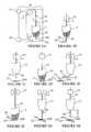
- the methodis performed on a substrate having a circuit side (first side in the claims), a back side (second side in the claims), and a through via.
- the steps of the methodcan be performed using a conventional wire bonder having a bonding capillary and an alignment system configured to align the bonding capillary to the via.
- the methodincludes the steps of threading a wire through the via, forming a back side contact on the wire proximate to the back side, forming a bonded contact on the wire on the circuit side, severing the wire from the bonded contact, and optionally forming a stud bump on the bonded contact.
- the methodforms a through wire interconnect which includes the wire in the via having the contact on the back side, and the bonded contact on the circuit side.
- the through wire interconnectcan be used to provide electrical and thermal paths through the substrate.
- the through wire interconnectcan also be used for stacking multiple semiconductor components, as it provides a bonding structure and a conductive path between stacked components.
- the wirehas a higher conductivity and a lower capacitance than conventional metal filled vias.
- the wirecan be configured to move in the via for accommodating variations in thermal expansion between the wire and the substrate.
- the viacan be filled with a material, which secures the wire in the via, and performs a desired function in the component.
- the materialcan comprise a dielectric material configured to change the capacitive coupling of the wire to the substrate, or to adjacent wires.
- the materialcan also be used to structurally strengthen and support the wire, and to electrically insulate the wire from the substrate.
- the materialcan comprise a thermally conductive material, configured to conduct heat through the substrate, such as away from active electrical elements.
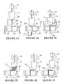
- An alternate embodiment stacked methodis performed on a stack of spaced substrates having spacers and aligned vias.
- the stacked methodincludes the steps of threading a wire through the aligned vias, forming a contact on the wire, pulling the contact against a first outer substrate of the stack, forming a bonded contact on a second outer substrate of the stack, and forming bonded connections between the substrates and the wire in the aligned vias.
- the stacked methodforms a stacked through wire interconnect that interconnects all of the substrates in the stack.
- the stacked methodcan also include the step of threading and bonding a side wire to the stacked through wire interconnect using a space between adjacent substrates.
- the systemincludes the substrate having the circuit side, the back side, and the via.
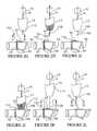
- the systemalso includes a wire bonder having a bonding capillary for threading, bonding and severing the wire, clamps or a wire threading mechanism for manipulating the wire, and a wand for forming the contact on the wire.
- An alternate embodiment systemincludes a wire bonder in combination with a stud bumper configured to form the stud bump on the bonded contact on the circuit side, or alternately a stud bump on the contact on the back side.
- Another alternate embodiment systemincludes a wire bonder having a first bonding capillary configured to perform steps from the circuit side of the substrate, and a second bonding capillary configured to perform steps from a back side of the substrate.
- Another alternate embodiment systemincludes a wire bonder having a side feed bonding capillary and a laser configured to bond a side wire between stacked substrates.
- the side feed bonding capillarycan be rotatable about a 90° angle for bonding on orthogonally oriented surfaces.
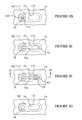
- the semiconductor componentincludes the substrate and the though wire interconnect.
- the through wire interconnectincludes the wire in the via having the bonded contact on the circuit side, and the contact on the back side.
- Multiple semiconductor componentscan stacked to form a stacked component having bonded connections between the bonded contacts on the circuit side, and the contacts on the back side, on adjacent components.
- An alternate embodiment interconnect componentincludes a through wire interconnect having the contact on the back side, or a separate contactor, configured to make non bonded electrical connections with test pads on a device under test.
- An alternate embodiment stacked array semiconductor componentincludes stacked semiconductor substrates interconnected by a single through wire interconnect.
- An alternate embodiment side wire semiconductor componentincludes stacked substrates, a side wire interconnect, and a side mounted component.
- the stacked substratescan include a heat sink, and the side mounted component can include a cooling assembly.
- An alternate embodiment compressed bump semiconductor componentincludes a through wire interconnect having a bonded contact in the form of compressed wire bump.
- An alternate embodiment organic semiconductor componentincludes an organic substrate, and a through wire interconnect bonded to contacts on the substrate. Alternately, the organic substrate can comprise a ceramic substrate or a metal substrate.
- An alternate embodiment flex circuit semiconductor componentincludes a substrate having a flex circuit attached thereto, and a through wire interconnect bonded to the flex circuit.
- FIGS. 1A-1Hare schematic cross sectional views of elements of the system illustrating set up steps in the method of the invention
- FIGS. 2A-2Lare schematic cross sectional views of elements of the system illustrating steps in the method of the invention.
- FIG. 3Ais a schematic plan view taken along line 3 A- 3 A of FIG. 2A illustrating a semiconductor wafer of the system;
- FIG. 3Bis an enlarged schematic plan view taken along line 3 B- 3 B of FIG. 3A illustrating a semiconductor substrate of the system;
- FIG. 3Cis an enlarged schematic cross sectional view taken along line 3 C- 3 C of FIG. 3B illustrating elements of the semiconductor substrate;
- FIG. 3Dis an enlarged schematic plan view taken along line 3 D- 3 D of FIG. 2C illustrating elements of the semiconductor substrate following a threading step of the method;
- FIG. 3Eis an enlarged schematic plan view taken along line 3 E- 3 E of FIG. 2G illustrating elements of the semiconductor substrate following a bonded contact forming step of the method;
- FIG. 3Fis an enlarged schematic plan view taken along line 3 F- 3 F of FIG. 2K illustrating elements of the semiconductor substrate following a stud bump forming step of the method;
- FIG. 3Gis an enlarged schematic plan view taken along line 3 G- 3 G of FIG. 2I illustrating elements of the semiconductor substrate prior to a new cycle of the method;
- FIG. 3His an enlarged schematic cross sectional view taken along line 3 H- 3 H of FIG. 3F illustrating elements of the semiconductor substrate following the stud bump forming step of the method;
- FIG. 3Iis an enlarged schematic cross sectional view equivalent to FIG. 3H illustrating elements of the semiconductor substrate following an optional wire encapsulating step of the method;
- FIG. 3Jis an enlarged schematic cross sectional view equivalent to FIG. 3H illustrating elements of the semiconductor substrate following an optional terminal contact forming step of the method;
- FIG. 4Ais a block diagram of a system for performing the method of the invention.
- FIG. 4Bis a block diagram of an alternate embodiment system for performing the method of the invention.
- FIGS. 5A and 5Bare schematic cross sectional views of another alternate embodiment system for performing the method of the invention.
- FIG. 6is a schematic cross sectional view of another alternate embodiment system for performing the method of the invention.
- FIG. 7Ais a schematic cross sectional view of another alternate embodiment system for performing the method of the invention.
- FIG. 7Bis an enlarged portion of FIG. 7A taken along line 7 B in FIG. 7A ;
- FIG. 8is a schematic cross sectional view of a stacked component constructed in accordance with the invention.
- FIG. 9is a schematic cross sectional view of a stacked, staggered component constructed in accordance with the invention.
- FIG. 10is a schematic cross sectional view of a stacked die component constructed in accordance with the invention.
- FIGS. 11A and 11Bare schematic cross sectional views of an interconnect component constructed in accordance with the invention.
- FIG. 12is a schematic cross sectional view of an interconnect component with a contactor constructed in accordance with the invention.
- FIGS. 13A-13Fare schematic cross sectional views illustrating steps in an alternate embodiment stacked method of the invention.
- FIG. 13Gis a view taken along line 13 G- 13 G of FIG. 13F with a cut away insulating layer;
- FIG. 14is a schematic cross sectional view of a stacked array semiconductor component and a module semiconductor component constructed using the stacked method
- FIG. 15A-15Dare schematic cross sectional views of stacked array side element semiconductor components and module semiconductor components constructed using the stacked method
- FIG. 16is a schematic cross sectional view of an alternate embodiment looped wire semiconductor component
- FIG. 17is a schematic cross sectional view of an alternate embodiment organic substrate semiconductor component.
- FIG. 18is a schematic cross sectional view of an alternate embodiment flex circuit semiconductor component.
- semiconductor componentmeans an electronic element that includes a semiconductor die, or makes electrical connections with a semiconductor die.
- wafer-levelmeans a process conducted on an element, such as a semiconductor wafer, containing multiple components.
- die levelmeans a process conducted on a singulated element such as a singulated semiconductor die or package.
- chip scalemeans a semiconductor component having an outline about the same size as the outline of a semiconductor die.
- a wire bonder 10( FIG. 1A ) can be provided.
- the wire bonder 10( FIG. 1A ) is configured to perform an ultra fine pitch (e.g., ⁇ 65 ⁇ m) wire bonding process.
- Suitable wire bondersare manufactured by Kulicke & Soffa Industries Inc. of Willow Grove, Pa., and SPT (Small Precision Tools) of Petaluma, Calif.
- One suitable wire bonderis a model “8098” large area ball bonder manufactured by Kulicke & Soffa Industries Inc., having a total bond placement accuracy of about +/ ⁇ 5 ⁇ m at pitches down to about 65 ⁇ m.
- the wire bonder 10includes a bonding capillary 12 configured to bond a continuous length of wire 14 to a first contact 20 A ( FIG. 1C ) on a substrate 22 ( FIG. 1C ).
- the first contact 20 A ( FIG. 1C ) and the substrate 22 ( FIG. 1C )can comprise dummies or set up elements.
- a representative diameter of the bonding wire 14can be from about 12 ⁇ m to about 150 ⁇ m.
- the bonding wire 14can comprise a conventional wire material used in semiconductor packaging, such as solder alloys, gold, gold alloys, copper, copper alloys, silver, silver alloys, aluminum, aluminum-silicon alloys, and aluminum-magnesium alloys.
- the wire 14can comprise a metal, or a metal alloy, that does not contain reductions of hazardous substances (ROHS), such as lead.
- ROHS free metalsinclude lead free solders, such as 97.5% Sn2.5% Ag.
- Other ROHS free metalsinclude gold, copper and alloys of these metals such as copper coated with a layer of flash gold.
- the melting point of the wire 14should preferably be greater than that of the substrate contact 20 A.
- the bonding capillary 12is movable in x, y and z directions responsive to signals from a controller 24 ( FIG. 1A ). As will be further explained, the bonding capillary 12 can also be configured for 90° rotation to allow side wire bonding.
- the bonding capillary 12includes an elongated opening 36 having an inside diameter about twice the diameter of the wire 14 , and an enlarged, chamfered terminal portion 36 A.
- the wire bonder 10also includes wire clamps 16 operably associated with the bonding capillary 12 , which are configured to open and close about the wire 14 responsive to signals from the controller 24 .
- the wire clamps 16are operably associated with a wire feed mechanism 17 configured to feed the wire 14 into the wire clamps 16 and the bonding capillary 12 .
- the wire feed mechanism 17can comprise a standard wire feed mechanism, such as one incorporated into the above described model “8098” large area ball bonder from Kulicke & Soffa.
- the wire feed mechanism 17can comprise a mechanical wire feeder mechanism, such as a roller feed mechanism, or a linear motion clamp and feed mechanism.
- the wire bonder 10also includes an alignment system 26 configured to ascertain the locations of the bonding capillary 12 and the first contact 20 A ( FIG. 1C ), and to supply information on these locations to the controller 24 for aligning the bonding capillary 12 to the first contact 20 A ( FIG. 1C ).
- the bonding capillary 12can comprise a stationary element, while the substrate 22 and the first contact 20 A are moved into alignment using a suitable mechanism (not shown).
- the wire bonder 10also includes an electronic flame off (EFO) wand 18 ( FIG. 1B ) configured to generate an electronic spark 28 ( FIG. 1B ) for forming a contact ball 30 ( FIG. 1B ) on a terminal portion 32 ( FIG. 1A ) of the wire 14 .
- EFOelectronic flame off
- the contact ball 30( FIG. 1B ) is also known in the art as a “free air ball” (FAB).
- the wire 14is threaded through the bonding capillary 12 with the terminal portion 32 of the wire 14 extending from the bonding capillary 12 .
- the electronic flame off (EFO) wand 18is operated to form the contact ball 30 on the terminal portion 32 ( FIG. 1A ) of the bonding wire 14 .
- a diameter of the contact ball 30will be dependent on the diameter of the wire 14 , with from 2 to 4 times the diameter of the wire 14 being representative.
- the diameter of the contact ball 30will be approximately equal to the chamfered portion 36 A of the opening 36 in the bonding capillary 12 .
- the bonding capillary 12is moved in the z direction towards the first contact 20 A on the substrate 22 , as indicated by arrow 34 , which captures the contact ball 30 in the chamfered opening 36 ( FIG. 1A ).
- the contact ball 30is pressed against the first contact 20 A with a selected force, and ultrasonic energy is applied to bond the contact ball 30 to the first contact 20 A and form a bonded contact 38 ( FIG. 1E ).
- the wire clamps 16open, and the bonding capillary 12 is moved in x and z directions (and if required y direction), as indicated by arrows 40 , 42 to perform a looping step.
- the bonding capillary 12presses an intermediate portion 44 of the wire 14 against a second contact 20 B on the substrate 22 with a selected force.
- ultrasonic energyis applied to form a second bonded contact in the form of a stitch bond 46 ( FIG. 1G ) between the wire 14 and the second contact 20 B.
- the bonding capillary 12is moved in the z direction away from the second contact 20 B for a selected distance, as indicated by arrow 48 , while the wire clamps 16 remain open.
- this severing stepforms a wire bonded wire 52 having the bonded contact 38 ( FIG. 1E ) bonded to the first contact 20 A ( FIG. 1E ), and the stitch bond 46 ( FIG. 1H ) bonded to the second contact 20 B ( FIG. 1G ).
- the terminal portion 50 of the wire 14has a tail length TL, which is the distance from the end of the bonding capillary 12 to the end of the wire 14 .
- the value of the tail length TLis determined by the movement of the bonding capillary 12 , and by the timing of the closure of the wire clamps 16 .
- the severing stepis performed such that the tail length TL, is approximately equal to a thickness T ( FIG. 2A ) of a semiconductor substrate 54 , plus the diameter of the contact ball 30 ( FIG. 1B ), plus a selected clearance distance.
- the terminal portion 50 of the wire 14can be smoothed and rounded using a process, such as a partial flame off, to facilitate subsequent threading of the wire 14 .
- FIGS. 2A-2I , and FIGS. 3A-3Gsteps in a method for fabricating a semiconductor component 86 ( FIG. 3J ) in accordance with the invention are illustrated.
- the methodis performed at the wafer level on a semiconductor wafer 56 ( FIG. 3A ) containing a plurality of the semiconductor substrates 54 .
- the method of the inventioncan be performed at the die level on singulated substrates, such as singulated bare dice and known good dice (KGD).
- the semiconductor wafer 56comprises a semiconductor material, such as silicon or gallium arsenide.
- the semiconductor substrates 54are in the form of semiconductor dice having a desired electrical configuration, such as memory, application specific, or imaging and image sensing.
- the method of the inventioncan be performed on other substrates including ceramic, plastic, tape, printed circuit board (PCB), metal lead frame, or flex circuit substrates.
- the semiconductor substrate 54includes a circuit side 62 (“first side” in some of the claims), and a back side 64 (“second side in some of the claims).
- the semiconductor substrate 54includes a plurality of substrate contacts 58 on the circuit side 62 , which in the illustrative embodiment comprise the device bond pads.
- the substrate contacts 58can comprise a highly-conductive, wire-bondable metal, such as aluminum, or a wire bondable and solderable metal, such as copper, or a combination of metals, such as solder coated metals.
- the semiconductor substrate 54is illustrated with only five substrate contacts 58 arranged in a single row. However, in actual practice the semiconductor substrate 54 can include tens of substrate contacts 58 arranged in a desired configuration, such as a center array, an edge array or an area array.
- the semiconductor substrate 54also includes a plurality of elongated RDL (redistribution layer) contacts 70 in electrical communication with the substrate contacts 58 .
- the RDL contacts 70are formed by a patterned redistribution layer on the circuit side 62 .
- the RDL contacts 70can comprise a highly-conductive, wire-bondable metal, such as aluminum, or a wire bondable and solderable metal, such as copper, or a combination of metals, such as solder coated metals.
- Redistribution layersare widely used in semiconductor manufacture to redistribute standard patterns of substrate contacts 58 into area arrays for terminal contacts.
- An exemplary redistribution layermight include “fan out” or “fan in” RDL conductors and terminal contact pads.
- the RDL contacts 70provide additional connection points for testing, such as probe testing of the semiconductor substrate 54 .
- U.S. Pat. No. 6,380,555 B1entitled “Bumped Semiconductor Component Having Test Pads, And Method And System For Testing Bumped Semiconductor Components”, which is incorporated herein by reference, describes an exemplary RDL circuit with additional test pads.
- the RDL contacts 70can comprise a same metal as the substrate contacts 58 , or alternately different metals than the substrate contacts 58 .
- the RDL contacts 70can include an additional solder layer, such as a lead free low melting point solder alloy, configured to facilitate a subsequent wire bonding step.
- the additional solder layercan be configured to melt at a temperature which is lower than that of the wire 14 , such that the wire is better able to maintain it's strength during wire bonding.
- the semiconductor substrate 54also includes an inner RDL insulating layer 72 between the RDL contacts 70 and the die passivation layer 68 , and an outer RDL insulating layer 74 on the inner RDL insulating layer 72 and on the RDL contacts 70 .
- the inner RDL insulating layer 72 , and the outer RDL insulating layer 74can comprise an electrically insulating polymer, such as polyimide.
- the outer RDL insulating layer 74includes openings 116 which align with portions of the RDL contacts 70 , and openings 117 which align with the substrate contacts 58 . As another option, the openings 116 and 117 can be combined into single elongated openings.
- through vias 76extend through the RDL contacts 70 , through the substrate contacts 58 , and through the semiconductor substrate 54 to the back side 64 thereof.
- the vias 76include via insulating layers 78 ( FIG. 3C ) formed on inside diameters thereof, which electrically insulate the vias 76 from the integrated circuits 66 and other electrical elements contained in the semiconductor substrate 54 .
- the insulating layers 78can comprise an electrically insulating material such as a polymer (e.g., polyimide or parylene) or an oxide (e.g., SiO 2 ).
- the vias 76can be formed using an etching process, a laser machining process, an ion milling process, a mechanical process (e.g., drilling, grinding, abrasion), or combinations of any of these processes.
- the vias 76can be formed using a dry etch process, such as a reactive ion etching (RIE) process.
- RIEreactive ion etching
- Another method for forming the vias 76combines etching and laser machining processes.
- an etch mask(not shown) and an etching process can be used to form the vias 76 through the RDL contacts 70 and the substrate contacts 58 .
- a wet etchantcan be used.
- RDL contacts 70 and substrate contacts 58 made of aluminumone suitable wet etchant is H 3 PO 4 .
- a laser machining processcan be used to form the vias 76 through the semiconductor substrate 54 .
- One suitable laser system for performing the laser machining stepis manufactured by XSIL LTD of Dublin, Ireland, and is designated a Model No. XISE 200.
- Another suitable laser system for performing the laser machining stepis manufactured by Electro Scientific, Inc., of Portland, Oreg. and is designated a Model No. 2700.
- a cleaning stepcan be performed in which the vias 76 are cleaned using a suitable wet or dry etchant.
- One suitable wet etchant with the semiconductor substrate 54 comprising siliconis tetramethylammoniumhydroxide (TMAH).
- parylene polymerscan be deposited from the vapor phase by a process similar to vacuum metallization at pressures of about 0.1 torr. Suitable polymers include parylene C, parylene N, and parylene D. Parylene is available from Advanced Coating of Tempe, Ariz.
- One suitable deposition apparatusis a portable parylene deposition system, designated a model PDS 2010 LABCOATER 2, manufactured by Specialty Coating Systems, of Indianapolis, Ind.
- silicon dioxidecan be grown by exposure of the semiconductor substrate 54 within the vias 76 to oxygen at an elevated temperature (e.g., 950° C.).
- Each via 76has a selected inside diameter which is about 1.5 to 3 times larger than the outside diameter of the wire 14 ( FIG. 2A ).
- the wire 14FIG. 2A
- the vias 76FIG. 3C
- a length of each via 76is dependent on an overall thickness T of the semiconductor substrate 54 ( FIG. 3C ).
- a representative range for the thickness T of the semiconductor substrate 54can be from about 50 ⁇ m to 725 ⁇ m depending on whether the wafer 56 ( FIG. 3A ) has a standard thickness or has been thinned.
- the thickness Twill include the thickness of the semiconductor material which forms the semiconductor substrate 54 ( FIG. 3C ), and the thickness of any additional elements such as the RDL insulating layers 72 , 74 ( FIG. 3C ) on the semiconductor substrate 54 ( FIG. 3C ).
- the bonding capillary 12is initially set up as previously described with the terminal portion 50 of the wire 14 having the tail length TL.
- an alignment stepis performed in which the bonding capillary 12 is moved to a position in which the terminal portion 50 of the wire 14 aligns with the center of a selected via 76 .
- the alignment stepcan be performed using the alignment system 26 ( FIG. 1A ), and the controller 24 ( FIG. 1A ) loaded with a program containing information on the locations of the substrate contacts 58 .
- the diameter of the via 76must be large enough relative to the diameter of the wire 14 to accommodate alignment tolerances of the alignment system 26 ( FIG. 1A ).
- a threading stepis performed in which the bonding capillary 12 is moved downward in the direction of arrow 88 ( FIG. 2A ) to thread the terminal portion 50 of the wire 14 through the via 76 .
- the terminal portion 50 of the wire 14projects from the back side 64 of the semiconductor component 54 by a predetermined distance.
- the bonding capillary 12can be set up with the end of the wire 14 flush with the chamfered portion 36 A ( FIG. 1A ) of the opening 36 ( FIG. 1A ) in the bonding capillary 12 .
- the opening 36 ( FIG. 1A )can then be aligned with the via 76 , and the wire feed mechanism 17 ( FIG. 1A ) operated to feed the end of the wire 14 through the via 76 until it extends from the back side 64 ( FIG. 3C ) of the semiconductor substrate 54 ( FIG. 2A ).
- a ball forming stepis performed in which the EFO wand 18 of the wire bonder 10 ( FIG. 1A ) is used to form a contact ball 90 on the end of the terminal portion 50 of the wire 14 .
- the contact ball 90has an outside diameter that is larger than the inside diameter of the via 76 .
- the ball forming stepcan be controlled using programmable EFO process parameters, such that a diameter of the contact ball 90 is from about 2 to 4 times the diameter of the via 76 .
- provisionscan be made to insure that the electronic spark goes only to the wire.
- the EFO wand 18can include a grounded metallic shield which prevents the electronic spark from contacting the semiconductor wafer 56 .
- the wire 14can be grounded to the wire bonder 10 ( FIG. 1A ) to insure the electronic spark does not jump to the semiconductor wafer 56 or the semiconductor substrate 54 .
- the ball forming stepcan be performed using a forming gas torch, such as a hydrogen gas torch, as is known in the art.
- a pulling and wedging stepis performed in which the bonding capillary 12 is moved upward as indicated by arrow 94 . Movement of the bonding capillary 12 also moves the contact ball 90 as indicated by arrow 96 , and wedges the contact ball 90 into the via 76 .
- the pulling and wedging stepis performed with the wire clamps 16 closed, and is substantially similar to the ball capture step previously described and shown in FIG. 1C . However, in this case, rather than being captured by the bonding capillary 12 , the contact ball 90 is pulled against the back side 64 ( FIG. 3C ) and wedged into the via 76 with a force exerted by the bonding capillary 12 . Gas pressures above and below the semiconductor substrate 54 can also be used to move and wedge the contact ball 90 into the via 76 .
- FIG. 3Dillustrates the wire 14 in the via following the pulling and wedging step.
- the contact ball 90FIG. 2C
- the wire 14FIG. 3D
- the wire 14remains unattached to the sidewall 100 ( FIG. 3D ) of the via 76 ( FIG. 2C ).
- the wire 14is free to move within the via 76 , such that in the completed component 86 ( FIG. 3J ) stresses are not generated during temperature cycling, due to the different thermal coefficients of expansion (TCE) of the wire 14 and the semiconductor substrate 54 .
- TCEthermal coefficients of expansion
- a looping stepis performed in which the wire clamps 16 are opened, and the bonding capillary 12 is moved in x and z directions (and also in the y direction if required) into alignment with the RDL contact 70 ( FIG. 3C ).
- the looping stepcan be performed using the alignment system 26 ( FIG. 1A ) and the controller 24 ( FIG. 1A ), substantially as previously described and shown for the looping step of FIG. 1F .
- the controller 24FIG. 1A
- the wire clamps 16remain open during the looping step.
- a bonded contact forming stepis performed in which a bonded contact 92 ( FIG. 2F ) is formed between an intermediate portion of the wire 14 and the RDL contact 70 .
- the bonded contact 92comprises a stitch bond formed using pressure and ultrasonic energy exerted by the capillary tool 12 , substantially as previously described and shown in FIG. 1G .
- the wire clamps 16remain open during the bonded contact forming step.
- FIG. 3Eillustrates the resultant through wire interconnect 102 .
- the through wire interconnect 102includes the bonded contact 92 bonded to the RDL contact 70 on the circuit side 62 of the semiconductor substrate 54 .
- the through wire interconnect 102includes the contact ball 90 ( FIG. 2F ) wedged into the via 76 on the back side 64 ( FIG. 2F ) of the semiconductor substrate 54 .
- optional additional stud bumping stepscan be performed for forming a stud bump 106 ( FIG. 2K ) on the bonded contact 92 .
- the stud bump 106 ( FIG. 2K )in addition to providing an external contact point to the through wire interconnect 102 , also provides a security bond for the bonded contact 92 .
- a separate stud bumper 124can be used to form the stud bump 106 ( FIG. 2K ).
- One suitable stud bumperis a “WAFER PRO PLUS” high speed large area stud bumper manufactured by Kulicke & Soffa Industries Inc. of Willow Grove, Pa.
- the wire 14can comprise a standard material, such as a solder alloy, copper, aluminum or palladium
- the stud bump 106FIG. 2K
- the wire 14can comprise a standard material, such as a solder alloy, copper, aluminum or palladium
- the stud bump 106FIG. 2K
- the EFO wand 18 of the wire bonder 10( FIG. 1A ) is used to form a contact ball 108 ( FIG. 2H ) on the terminal portion 110 ( FIG. 2G ) of the wire 14 , substantially as previously described and shown in FIG. 1B .
- the bonding capillary 12is moved to capture the contact ball 108 substantially as previously described and shown in FIG. 1C .
- the bonding capillaryis aligned with the bonded contact 92 , and the bonding capillary 12 is moved towards the bonded contact 92 , as indicated by arrow 104 .
- force and ultrasonic energyare applied by the bonding capillary 12 , as indicated by arrow 112 , to bond the contact ball 108 to the bonded contact 92 .
- FIG. 2Killustrates the bonding capillary 12 in a plan view.
- FIG. 3Hillustrates the through wire interconnect 102 with the stud bump 106 on the semiconductor substrate 54 in a cross sectional view.
- FIG. 3Gillustrates the next via 76 , the substrate contact 58 and the RDL contact 70 prior to the next threading step.
- the through wire interconnect 102 and the semiconductor substrate 54are illustrated in cross section after an optional wire encapsulating step has been performed.
- a wire encapsulant 80has been deposited in the via 76 to encapsulate the portion of the through wire interconnect 102 in the via 76 .
- the wire encapsulant 80can comprise a polymer, such as a UV or thermal curable epoxy, deposited into the via 76 using a suitable process such as capillary injection, or screen printing. Following deposition, the wire encapsulant 80 can be cured to harden.
- the wire encapsulant 80attaches the through wire interconnect 102 to the via 76 , performing a locking function, and providing another layer of electrically insulating dielectric material between the through wire interconnect 102 and the semiconductor substrate 54 .
- the wire encapsulant 80electrically insulates the contact ball 90 , and prevents shorting between the contact ball 90 and the semiconductor substrate 54 .
- the wire encapsulant 80can also be configured to adjust a capacitance of the through wire interconnect 102 .
- a no-sweep encapsulant 246( FIG. 13G ) can be deposited on the through wire interconnects 102 to prevent wire sweep.
- Kulicke & Soffamanufactures a product under the trademark “NOSWEEP” encapsulant, which can be dispensed and cured during operation of the wire bonder 10 ( FIG. 1A ).
- terminal contacts 84such as flip chip solder balls (OLB balls) or FCOM balls, are formed on the semiconductor substrate 54 in electrical communication with the through wire interconnect 102 .
- conductors 82 and terminal contact bonding pads 118have been formed on the outer RDL insulating layer 74 in electrical communication with the bonded contacts 92 and with the RDL pads 70 .
- terminal contacts 84have been formed on the terminal contact bonding pads 118 .
- the conductors 82 and the terminal contact bonding pads 118are shown as separate layers for illustrative purposes. However, the conductors 82 and the terminal contact bonding pads 118 are preferably part of the redistribution layer that forms the RDL pads 70 , and are preferably formed prior to the threading step shown in FIG. 2A .
- the terminal contacts 84can be mounted in openings through the outer RDL insulating layer 74 directly to RDL conductors having a same thickness as the RDL contacts 70 .
- the terminal contacts 84can be formed using a suitable process such as solder ball bonding or stud bumping. As will be further explained, the terminal contacts 84 can be used to provide external connection points and a flip chip bonding structures to a circuit board or other supporting substrate.
- the semiconductor substrate 54FIG. 3A
- the semiconductor substrate 54can be singulated from the wafer 56 ( FIG. 3A ) using a suitable process such as cutting, shearing, etching or water jetting.
- the completed semiconductor component 86includes the semiconductor substrate 54 containing the integrated circuits 66 .
- the semiconductor component 86includes the through wire interconnect 102 in electrical communication with the substrate contacts 58 , the RDL contacts 70 and the integrated circuits 66 .
- the through wire interconnect 102includes the contact ball 90 ( FIG. 2F ) wedged into the via 76 on the back side 64 ( FIG. 2F ) of the semiconductor substrate 54 .
- the through wire interconnect 102also includes the bonded contact 92 with the stud bump 106 on the RDL contact 70 on the circuit side 62 .
- the contact ball 90 and the bonded contact 92permit the semiconductor component 86 to be stacked on other components.
- the semiconductor component 86also includes terminal contacts 84 on the circuit side 62 in electrical communication with the through wire interconnect 102 and with the integrated circuits 66 .
- the semiconductor component 86has a chip scale outline which matches that of the semiconductor substrate 54 .
- the system 120includes the wire bonder 10 which includes the bonding capillary 12 ( FIG. 1A ), the wire clamps 16 ( FIG. 1A ), the alignment system 26 ( FIG. 1A ), the controller 24 ( FIG. 1A ) and the EFO wand 18 ( FIG. 1B ). Each of these elements functions substantially as previously described.
- the systemalso includes the semiconductor wafer 56 containing the semiconductor substrate 54 having the via 76 , the RDL contacts 70 , and all of the other previously described elements.
- an alternate embodiment system 122includes essentially the same elements as the system 120 ( FIG. 4A ), but also includes a stud bumper 124 for performing the stud bumping step in which the stud bumps 106 ( FIG. 2K ) are formed on the bonded contacts 92 ( FIG. 2K ).
- an alternate embodiment system 126includes a wire bonder 10 A, which is substantially equivalent to the previously described wire bonder 10 ( FIG. 1A ).
- the wire bonder 10 Aincludes a first bonding capillary 12 A configured to perform steps of the invention from the circuit side 62 of the semiconductor substrate 54 , and a second bonding capillary 12 B configured to perform steps of the invention from the back side 64 of the semiconductor substrate 54 .
- the second bonding capillary 12 Bcan be used to form, and then to exert a pressure on the contact ball 90 , as indicated by arrow 128 , to wedge the contact ball 90 in the via 76 .
- the via 76includes a metal layer the second bonding capillary 12 B can be used to bond the contact ball 90 to the metal layer using ultrasonic or thermal energy.
- the system 126 and the second bonding capillary 128can be used to form a stud bump 106 A “on”, or “in place of” the contact ball 90 .
- the stud bump 106 Acan be substantially equivalent to the stud bump 106 ( FIG. 3H ) previously described.
- the stud bump 106 Acan be used to interconnect stacked components.
- an alternate embodiment system 130includes the two bonding capillaries 12 A, 12 B, and also includes a pusher mechanism 132 which is movable as indicated by arrow 138 .
- the pusher mechanism 132can be used to push the contact ball 90 onto a back side contact 136 on the semiconductor substrate 54 .
- the second bonding capillary 12 Bcan then be moved as indicated by arrow 138 to bond the contact ball 90 to the back side contact 136 .
- an alternate embodiment system 144includes the two bonding capillaries 12 A, 12 B configured substantially as previously described.
- the system 144also includes a thinned semiconductor wafer 56 T having a thinned semiconductor substrate 54 T having a thickness of about 25 ⁇ m to 200 ⁇ m.
- the thinned semiconductor substrate 54 Tincludes a via 76 T and an RDL contact 70 T, which are constructed substantially as previously described for the via 76 ( FIG. 2A ) and the RDL contact 70 ( FIG. 2A ).
- the via 76 Tdoes not extend through the RDL contact 70 T, and the length of the via 76 T is about the same as the diameter of a contact ball 90 T.
- the second capillary 12 Bis configured to form the contact ball 90 T from the wire 14 , and to bond the contact ball 90 T (and also another end of the wire 14 , if desired), substantially as previously described.
- the first bonding capillary 12 Ais configured as a “backing”, “support” or “anvil” capillary, which as indicated by arrow 140 resists the pressure of the second bonding capillary 12 B.
- the RDL contact 70 Tcan include a through hole allowing the bonding capillary 12 A to feed the wire 14 through the hole, form a free air ball (FAB), pull away, make a wire loop, and then make a security or stud bond on the surface of RDL contact 70 T.
- FABfree air ball
- Both bonding capillaries 12 A, 12 Bcould form a bond on the outer and inner surfaces of the RDL contact 70 T, or form a wire rivet through the RDL contact 70 T.
- the second bonding capillary 12 Bcan be configured as an electrically conductive spot welder such that the contact ball 90 T can be welded to the back side of the RDL contact 70 T.
- the stacked component 146includes the semiconductor component 86 with the through wire interconnects 102 having the contact balls 90 on the back side 64 , and the conductors 82 and the terminal contacts 84 on the circuit side 62 .
- three separate semiconductor components 86 - 1 , 86 - 2 and 86 - 3are stacked on the semiconductor component 86 .
- the semiconductor components 86 - 1 , 86 - 2 and 86 - 3are substantially identical to the semiconductor component 86 , but do not include the terminal contacts 84 or the conductors 82 .
- the balls 90 , or stud bumps 106 AFIG.
- bonded interconnect connections 170can comprise solder joints, mechanical connections, welded connections, or conductive polymer connections formed between the contact balls 90 and the wires of the through wire interconnects 102 .
- an underfill material 162FIG. 10 can be formed in the gaps 164 between adjacent components.
- the stacked component 154includes the semiconductor component 86 with the through wire interconnects 102 having the contact balls 90 on the back side 64 , and the conductors 82 and the terminal contacts 84 on the circuit side 62 .
- three separate semiconductor components 86 - 1 S, 86 - 2 S and 86 - 3 Sare stacked on the semiconductor component 86 .
- the semiconductor components 86 - 1 S, 86 - 2 S and 86 - 3 Sare substantially identical to the semiconductor component 86 , but do not include the terminal contacts 84 .
- the contact balls 90 , or stud bumps 106 AFIG.
- bonded interconnect connections 172are between adjacent contact balls 90 , or stud bumps 106 A ( FIG. 5B ), and the stud bumps 106 of the bonded contacts 92 ( FIG. 3J ).
- the bonded interconnect connections 172can comprise solder joints, mechanical connections, welded connections, or conductive polymer connections formed between the contact balls 90 and the stud bumps 106 .
- the semiconductor components 154 , 86 - 1 S, 86 - 2 S and 86 - 3 Sare staggered by a distance approximately equal to the distance between the stud bumps 106 and the vias 76 .
- the offset between adjacent componentsis not to scale, as this distance will typically be on the order of only about 100-300 ⁇ m.
- a stacked die component 148includes a semiconductor die 150 stacked and bonded to the semiconductor component 86 .
- the semiconductor die 150includes die contacts 152 bonded to the contact balls 90 , or stud bumps 106 A ( FIG. 5B ), of the through wire interconnects 102 , forming bonded interconnect connections 174 there between.
- the bonded interconnect connections 174can comprise solder joints, mechanical connections, welded connections, or conductive polymer connections formed between the contact balls 90 , or stud bumps 106 A ( FIG. 5B ), and the die contacts 152 .
- an underfill layer 162such as a curable polymer, can be formed between the semiconductor component 86 and the semiconductor die 150 .
- the semiconductor component 86can be contained on the semiconductor wafer 56 ( FIG. 3A ), such that wafer scale stacked components can also be provided.
- interconnect component 86 Iis illustrated.
- the interconnect component 86 Iis substantially identical to the semiconductor component 86 ( FIG. 3J ), but is configured for conducting test signals from the terminal contacts 84 through the through wire interconnects 102 to the balls 90 , or stud bumps 106 A ( FIG. 5B ).
- a device under test 156such as a semiconductor die or wafer, includes test pads 160 .
- the device under test 156can be moved into engagement with the interconnect substrate 86 I using a suitable apparatus such as a probe tester or single die carrier.
- the interconnect component 86 Idoes not necessarily include the integrated circuits 66 ( FIG. 3C ), as it can be a passive element configured to make non bonded electrical connections 176 ( FIG. 11B ) with the device under test 156 .
- the interconnect component 86 Idoes not necessarily need to be made of a semiconductor material but can comprise a ceramic, a plastic material or a composite material.
- the through wire interconnect 102can optionally be free to move in the via 76 with the loop allowing flexure without fatigue. In this case, the through wire interconnect 102 can be springy enough in an unloaded state to keep the ball 90 in a position away from the outer surface of the interconnect component 86 I.
- the through wire interconnect 102can be encapsulated in the via 76 as previously described, but with the ball 90 free to move up and down in the z-direction.
- the ball 90can be plated with a wear resistant metal having a high electrical conductivity.
- the ball 90could function as a mini “POGO PIN” for use in probe cards and known good die (KGD) test sockets, with the via encapsulant protecting and preventing buckling of the through wire interconnect 86 I.
- interconnect component 86 ICis illustrated.
- the interconnect component 86 ICis substantially identical to the interconnect component 86 I ( FIG. 11A ).
- the interconnect component 86 ICincludes separate test contactors 186 in electrical communication with the through wire interconnects 102 configured to make non bonded electrical connections 178 with the test contacts 160 on the device under test 156 .
- the test contactors 168can comprise raised contacts with penetrating projections as described in U.S. Pat. No. 5,483,741 entitled “Method For Fabricating A Self Limiting Silicon Based Interconnect For Testing Bare Semiconductor Dice”, which is incorporated herein by reference.
- the test contactors 168can be constructed as described in U.S. Pat. No. 5,931,685 entitled “Interconnect For Making Temporary Electrical Connections With Bumped Semiconductor Components”, which is incorporated herein by reference.
- steps in an alternate embodiment stacked methodare illustrated for forming a stacked array component 86 SA ( FIG. 13E ).
- the stacked methodcan be performed at the wafer level on a semiconductor wafer 56 ( FIG. 3A ) containing a plurality of the semiconductor substrates 54 .
- the stacked methodcan be performed on singulated semiconductor substrates 54 , such as bare dice or known good dice (KGD).
- FIG. 13Afour semiconductor substrates 54 A- 54 D are stacked with spacers 182 there between to form a stacked array 180 .
- the uppermost substrate of the stacked array 180( FIG. 13A ) is termed herein as the first outer semiconductor substrate 54 A.
- the lowermost substrate of the stacked array 180( FIG. 13A ) is termed herein as the second outer semiconductor substrate 54 D.
- the middle substrates 54 B and 54 C of the stacked array 180( FIG. 13A ) are termed herein as the inner semiconductor substrates 54 B and 54 C.
- the spacers 182can comprise a metal such as solder, or a polymer, such as an epoxy or resist.
- the spacers 182can be formed directly on the semiconductor substrates 54 A- 54 D, or on special pads (not shown) on the semiconductor substrates 54 A- 54 D, using a process such as stud bumping, ball bonding, screen printing, dot shooting, nozzle deposition, or photopatterning.
- the spacers 182form spaces 214 A- 214 C ( FIG. 13A ) between adjacent semiconductor substrates 54 A- 54 D having a spacing S which is equal to the height of the spacers 182 .
- a representative range for the spacing Scan be from 10 ⁇ m to 100 ⁇ m.
- the spacers 182FIG. 13A
- the spacers 182FIG. 13A
- the spacers 182FIG. 13A
- the spacers 182FIG.
- the spacers 182preferably allow some relative movement or shifting laterally between the semiconductor substrates 54 A- 54 D.
- the spacers 182can be configured to providing bearings for moving the semiconductor substrates 54 A- 54 D relative to one another.
- the spacers 182provide a material between the semiconductor substrates 54 A- 54 D, which can be configured to provide protection from mechanical, electrical or magnetic influences (e.g., adding an electrical ground plane, or to shield the substrates from stray magnetic fields).
- the spaces 214 A- 214 C ( FIG. 13A ) created by the spacers 182are maintained throughout the steps of the method, and in the completed semiconductor component 86 SA ( FIG. 13A ) as well.
- the spaces 214 A- 214 C ( FIG. 13A )facilitate the performance of other steps of the method, such as: a.) bonding, by permitting formation of a column of material (e.g., solder) between adjacent semiconductor substrates 54 A- 54 D, and b.) laser machining, by providing access for a laser beam.
- the spaces 214 A- 214 C ( FIG. 13A )allow fluids for cooling or heating the semiconductor substrates 54 A- 54 D, or for placing a material, such as an underfill layer, or a thermally conductive material, between the semiconductor substrates 54 A- 54 D.
- Each semiconductor substrate 54 A- 54 Dalso includes a through via 76 A- 76 D ( FIG. 13A ) formed through a substrate contact 58 A- 58 D ( FIG. 13A ), substantially as previously described for through via 76 ( FIG. 3C ) and the substrate contact 58 ( FIG. 3C ) on semiconductor substrate 54 ( FIG. 3A ).
- the substrate contacts 58 A- 58 Dcan be in electrical communication with integrated circuits 66 ( FIG. 3C ), and can include insulating layers 78 ( FIG. 3C ) substantially as previously described.
- the first outer semiconductor substrate 54 Aalso includes RDL contacts 70 A ( FIG. 13A ), substantially as previously described for RDL contacts 70 ( FIG. 3B ).
- the first outer semiconductor substrate 54 Aincludes conductors 82 A ( FIG. 13A ), and terminal contacts 84 A ( FIG. 13A ) in electrical communication with the RDL contacts 70 A ( FIG. 13A ), substantially as previously described for conductors 82 ( FIG. 3J ) and terminal contacts 84 ( FIG. 3J ).
- the conductors 82 Acan be part of the same redistribution layer that forms the RDL contacts 70 .
- the inner semiconductor substrates 54 B and 54 C ( FIG. 13A ), and the second outer semiconductor substrate 54 D as well,include bonding elements 184 ( FIG. 13A ) on their substrate contacts 58 B- 58 D ( FIG. 13A ).
- the bonding elements 184can comprise circular or polygonal donuts having through openings corresponding in size and shape to the through vias 76 B-D. Alternately, the bonding elements 184 ( FIG. 13A ) can simply comprise dots or mounds of material on the substrate contacts 58 B- 58 D.
- the bonding elements 184can be made of a low melting point metal, such as nickel, a nickel alloy, a solder alloy, gold or a gold alloy.
- the bonding elements 184can be made of a conductive polymer material.
- the bonding elements 184can be formed using a suitable process such as screen printing, deposition through a mask, reflow or polymer curing. As will be further explained, following a heating step, and a shifting step to be described, the bonding elements 184 form bonded connections 186 ( FIG. 13E ) between the substrate contacts 58 B- 58 D and the wire 14 .
- a bottle neck bonding capillary 12 BNis provided.
- a wire feed mechanism 17 BNis operably associated with the bonding capillary 12 BN, substantially as previously described for wire feed mechanism 17 ( FIG. 1A ).
- the wire feed mechanism 17 BNcan also be operably associated with clamps 16 ( FIG. 1A ), which for simplicity is not shown in FIGS. 13A-13F .
- this embodiment of the methodis described with the bottle neck bonding capillary 12 BN, the bonding capillary 12 ( FIG. 1A ), or a laser, could also be used.
- the bonding capillary 12 BN( FIG. 13A ) can comprise an element of a wire bonder, such as the previously described bonding capillary 12 ( FIG. 1A ) configured to perform an ultra fine pitch (e.g., ⁇ 65 ⁇ m) wire bonding process.
- Suitable bottle neck bonding capillariesare manufactured by SPT (Small Precision Tools) of Petaluma, Calif.
- SPTStandard Precision Tools
- One suitable bonding capillaryis designated as a molded slim line bottleneck (SBN) capillary.
- Kulicke & Soffa Industries Inc. of Willow Grove, Pa.also manufactures suitable bonding capillaries.
- the semiconductor substrates 54 A- 54 Dare aligned and attached to form the stacked array 180 .
- the stacked array 180all of the through vias 76 A are aligned along a common longitudinal axis 216 within a tolerance of plus or minus 5-10 ⁇ m.
- Alignment of the semiconductor substrates 54 A- 54 D, and forming of the spacers 182can be accomplished using equipment and techniques known in the art, such as aligner bonders, mechanical fixtures and reflow ovens.
- the bonding capillary 12 BNis aligned with the via 76 A in the first outer semiconductor substrate 54 A.
- a threading stepis performed by operating the wire feed mechanism 17 BN to thread the wire 14 through the aligned vias 76 A- 76 D such that the end 218 of the wire 14 projects from a back side 64 D of the second outer semiconductor substrate 54 D.
- the threading stepcan be performed substantially as previously described in FIG. 2A , by forming the tail length TL ( FIG. 2A ) of the wire 14 and then moving the bonding capillary 12 in the z-direction.
- a ball forming stepis performed in which the EFO wand 18 is used to form a contact ball 90 on the terminal portion of the wire 14 , substantially as previously described and shown in FIG. 2B .
- a pulling and wedging stepis performed to pull the contact ball 90 against the back side 64 D of the second outer semiconductor substrate 54 D, and to wedge the contact ball 90 into the via 76 D.
- a stitch bonding stepis performed in which a bonded contact 92 is formed on the RDL contact 70 A on the first outer semiconductor substrate 54 A.
- a severing stepis performed substantially as previously described to sever the wire 14 from the bonded contact 92 .
- the completed through wire interconnect 102 SA( FIG. 13A ) includes a length of the wire 14 threaded through the aligned vias 76 A- 76 D.
- the through wire interconnect 102 SAalso includes the contact ball 90 on the back side 64 D of the second outer semiconductor component 54 D, and the bonded contact 92 on the RDL contact 70 A on the first outer semiconductor substrate 54 A.
- a bonding stepis performed in which the bonding elements 184 are bonded to the wire 14 to form bonded connections 186 .
- a shifting stepcan be performed in which the middle semiconductor substrates 54 B, 54 C are shifted in opposite directions (or in the same direction) as indicated by arrows 210 , 212 .
- the shifting stepcan be performed using a suitable mechanism such as a pusher rod.
- the shifting steppinches the wire 14 , such that it touches the aligned vias 58 A- 58 D and contacts the bonding elements 184 .
- the shifting stepis preferably done such that the alignment of the vias 58 A- 58 D is only shifted by several microns.
- the inner semiconductor substrate 54 Bcan be shifted to the right by from 5 ⁇ m to 15 ⁇ m, and the inner semiconductor substrate 54 C can be shifted to the left by from 5 ⁇ m to 15 ⁇ m, for a total shift of from 10 ⁇ m to 30 ⁇ m.
- the spacers 182can be configured to facilitate the shifting step by providing bearing surfaces.
- the bonding stepcan be performed using a laser 220 configured to direct a laser beam 222 through the spaces 214 A, 214 B, 214 C ( FIG. 13A ) between the semiconductor substrates 54 A- 54 D.
- the laser beam 222is focused upon the bonding elements 184 ( FIG. 13D ), one bonding element 184 at a time, to provide localized heating for melting and reflowing the bonding elements 184 .
- the reflowed bonding elements 184form bonded connections 186 between the substrate contacts 58 B- 58 D and the wire 14 .
- the bonded connections 186electrically and structurally connect the semiconductor substrates 54 A- 54 D to one another.
- Suitable laser systems for performing the laser machining stepare manufactured by XSIL LTD of Dublin, Ireland, and by Electro Scientific, Inc., of Portland, Oreg.
- the completed stacked array semiconductor component 86 SAincludes the stacked array 180 , and the through wire interconnect 102 SA which electrically connects the semiconductor substrates 54 A- 54 D. If the semiconductor substrate 54 A- 54 D comprise semiconductor dice, the stacked array semiconductor component 86 SA can be referred to as a stack of die (SOD).
- SODstack of die
- a stacked module semiconductor component 86 Mincludes the stacked array semiconductor component 86 SA, and a CPU component 190 mounted to a supporting substrate 192 , to form a module, such as an imager module, or a memory-microprocessor module.
- the terminal contacts 84 A ( FIG. 13E ) of the stacked module semiconductor component 86 Mcan be bonded to electrodes 194 on the supporting substrate 192 .
- an optional additional through wire interconnect 198placed through opening 196 can be used to electrically connect other elements on the supporting substrate 192 to selected contact points on the stacked array 180 .
- an optional additional side wire feed and bond stepcan be performed to form a side wire semiconductor component 86 SF which includes side wire interconnects 188 .
- a side feed bonding capillary 12 SF, and an associated wire feed mechanism 17 SFcan be used to thread side wires 188 in the space 214 B between the inner semiconductor substrates 54 B and 54 C.
- the laser 220can be used to direct the laser beam 222 through the space 214 B to form the bonded connections 186 and bond the side wires 188 to the bonded connections 186 .
- the side wire feed and bond stepcan be performed by rotating the stacked array 180 ( FIG. 13F ) ninety degrees and aligning the side feed bonding capillary 12 SF to the space 214 B.
- Side feedingcan be self guiding by the dimensions of the space 214 B, or an alignment structure, such as a pattern resist, can be formed in the space 214 B.
- a real time alignment systemsuch as an x-ray vision system can be used to adjust the path of the wire 14 in the manner of a medical procedure for threading a catheter through an artery.
- side feedingcan be performed using an electrical sensing system configured to sense the point at which the wire 14 touches the bonding elements 184 ( FIG. 13D ).
- side feedingcan be performed using a guide tube attached to the side feed bonding capillary 12 SF configured to guide the wire 14 through the space 214 B.
- the laser 220( FIG. 13F ) can be operated in conjunction with the side feed bonding capillary 12 SF ( FIG. 13F ) to form the bonded connections 186 ( FIG. 13G ).
- the laser 220can fire to melt the bonding element 184 ( FIG. 13D ) as the side wire 188 is pushed into the molten material. Cooling of the molten material then forms the bonded connections 186 ( FIG. 13G ).
- a support layer 246 formed of a curable polymer, such as a UV curable epoxy or parylene,can be formed in the space 214 B to prevent movement and wire sweep of the side wires 188 ( FIG. 13G ). Conventional underfill materials can be used to form the support layer 246 .
- One suitable material for forming the support layer 246is the previously described wire sweep encapsulant sold by Kulicke & Soffa under the trademark “NOSWEEP” encapsulant.
- the side wire semiconductor component 86 SFcan include a side mounted element 206 such as a capacitor, another semiconductor substrate, a semiconductor package or a cooling assembly.
- the completed side feed through wire interconnect 102 SFincludes the side wire 188 bonded to the side mounted element 206 .
- a semiconductor component 86 Nincludes the side wire semiconductor component 86 SF and the CPU component 190 mounted to a supporting substrate 202 , substantially as previously described for module component 86 M ( FIG. 14 ).
- the semiconductor component 86 Ncan include a first side wire 188 and a second side wire 188 A bonded to the CPU component 190 and to the wire 14 .
- an opening 248 in the side mounted element 206provides access for the laser beam 222 ( FIG. 13F ) for bonding the second side wire 188 A.
- the bonding capillary 12 SF( FIG. 13F ) can be configured for rotation by 90° from the position shown in FIG. 13F .
- the CPU component 190can also include a riser substrate 250 , and a second side wire 188 B bonded to the riser substrate 250 .
- the riser substrate 250can comprise a printed circuit board, a ceramic substrate, a plastic substrate, a metal substrate, or other element, having conductors and wire bond pads in a required configuration. As shown in FIG.
- the side wire semiconductor component 86 SFcan also include a heat sink 252 .
- the side mounted element 206can include a cooling assembly 254 having a cooling fan 256 .
- the side mounted element 206can comprise a substrate housing a CPU to memory buffer-bridging device (like a NORTHBRIDGE chipset or an INTEL HUB ARCHITECTURE (IHA) chip set).
- the side mounted element 206could include a socket for mounting a side mountable CPU package attached to the cooling assembly 254 .
- the looped wire semiconductor component 86 LWincludes the semiconductor substrate 54 , the via 76 , the insulating layer 78 , the substrate contact 58 , the internal conductor 90 , the integrated circuits 66 , and the passivation layer 68 , all of which are constructed substantially as previously described.
- the looped wire semiconductor component 86 LWalso includes a through wire interconnect 102 LW ( FIG. 16 ) formed by looping the wire 14 into a looped wire 224 ( FIG. 16 ), which is then compressed to form a compressed bump 226 ( FIG. 16 ).
- the looped wire 224can be formed, and compressed into the bump 226 , using the bonding capillary 12 ( FIG. 2A ).
- the looped wire semiconductor component 86 LW ( FIG. 16 )can be used to fabricate a stacked component similar to the stacked component 146 ( FIG. 8 ). In this case the through wire interconnect 102 LW can be used to make bonded connections between adjacent looped wire semiconductor components 86 LW.
- the semiconductor component 860 Sincludes an organic substrate 540 S made of an organic material, such as a circuit board material, a glass filled polymer or a plastic.
- the semiconductor component 860 Scan be in the form of a printed circuit board, a flex circuit, a TAB tape, a leadframe, a BOC semiconductor package, a COB semiconductor package, or a chip scale semiconductor package.
- the semiconductor component 860 S ( FIG. 17 )also includes a conductive trace 228 ( FIG. 17 ) having a wire bondable contact 230 ( FIG. 17 ), and a polymer insulating layer 234 ( FIG. 17 ).
- the semiconductor component 860 S ( FIG. 17 )also includes a through wire interconnect 1020 S ( FIG. 17 ) formed in a through via 760 S ( FIG. 17 ) in the organic substrate 540 S ( FIG. 17 ) substantially as previously described for through wire interconnect 102 ( FIG. 3E ).
- the through wire interconnect 1020 S ( FIG. 17 )includes a contact ball 900 S ( FIG. 17 ) in contact with the organic substrate 540 S ( FIG. 17 ), and optionally with a back side contact 232 ( FIG. 17 ) on the organic substrate 540 S ( FIG. 17 ).
- the through wire interconnect 1020 Salso includes a stitch bond 460 S ( FIG. 17 ) bonded to the conductive trace 228 ( FIG. 17 ).
- the semiconductor component 86 FCincludes a substrate 54 FC having a flex circuit 236 attached thereto.
- the substrate 54 FCcan comprise a ceramic, a plastic, a metal, or a semiconductor material.
- the flex circuit 236includes dielectric layers 238 , 240 formed of a flexible polymer material (e.g., polyimide tape), and a conductive trace 244 sandwiched between the dielectric layers 238 , 240 .
- an adhesive layer 242attaches the flex circuit 236 to the substrate 54 FC.
- the semiconductor component 86 FC( FIG. 18 ) also includes a through wire interconnect 102 FS ( FIG. 18 ) formed in a through via 76 FS ( FIG. 18 ) in the substrate 54 FS ( FIG. 18 ) substantially as previously described for through wire interconnect 102 ( FIG. 3E ).
- the through wire interconnect 102 FS( FIG. 18 ) includes a contact ball 90 FS ( FIG. 18 ) in contact with the substrate 54 FS (FIG. 18 ), and a stitch bond 46 FS ( FIG. 18 ) bonded to the conductive trace 244 ( FIG. 18 ).
- the semiconductor component 86 FCcould be used as a test interconnect configured as a probe card, or a known good die carrier.
- the wire 14could be encapsulated in the via 76 FS, but with the contact ball 90 FS free to move upon contact with a test pad of a device under test, substantially as previously described for the contact ball 90 of FIGS. 11A and 11B .
Landscapes
- Engineering & Computer Science (AREA)
- Microelectronics & Electronic Packaging (AREA)
- Power Engineering (AREA)
- Computer Hardware Design (AREA)
- Physics & Mathematics (AREA)
- Condensed Matter Physics & Semiconductors (AREA)
- General Physics & Mathematics (AREA)
- Manufacturing & Machinery (AREA)
- Mechanical Engineering (AREA)
- Wire Bonding (AREA)
- Printing Elements For Providing Electric Connections Between Printed Circuits (AREA)
- Combinations Of Printed Boards (AREA)
Abstract
Description
- This invention relates generally to semiconductor packaging, and particularly to a method and system for fabricating semiconductor components with through wire interconnects. This invention also relates to semiconductor components having through wire interconnects fabricated using the method and system.
- A semiconductor component includes a semiconductor substrate containing various semiconductor devices and integrated circuits. Typically, the semiconductor substrate comprises a semiconductor die, that has been singulated from a semiconductor wafer. For example, a chip scale semiconductor component includes a semiconductor die provided with support and protective elements, and an external signal transmission system. Semiconductor components can also include multiple semiconductor substrates in a stacked or planar array. For example, a system in a package (SIP) includes multiple semiconductor dice packaged in a plastic body. A semiconductor component can also include a support substrate, such as a module substrate, a test substrate, or a printed circuit board, configured to electrically engage a semiconductor substrate.
- As semiconductor components become smaller and have higher input/output configurations, different types of interconnects have been developed for implementing different signal transmission systems. Interconnects can be formed “on” the semiconductor substrate for transmitting signals in x and y directions. Interconnects can also be formed “in” the semiconductor substrate for transmitting signals in a z direction, or “external” to the semiconductor substrate for transmitting signals in x, y and z directions.
- For example, surface interconnects, such as conductors “on” a circuit side of the semiconductor component, can be used to electrically connect the integrated circuits with terminal contacts on the circuit side. Via interconnects, such as metal filled vias formed “in” the semiconductor substrate, can be used to electrically connect the integrated circuits to terminal contacts on a back side of the semiconductor substrate. Wire interconnects, such as wires bonded to the semiconductor substrate, can be used to electrically connect the integrated circuits to “external” terminal contacts on a support substrate for the component.
- In fabricating semiconductor components, particularly chip scale components, interconnects having a high electrical conductivity and a low parasitic capacitance provide the best performance in the signal transmission system. In addition, it is advantageous for interconnects to be capable of fabrication in dense arrays using conventional equipment and techniques. Further, it is advantageous for interconnects to require as little space and additional elements as possible. In this regard, each of the different types of interconnects has advantages and disadvantages.
- One significant advantage of via interconnects is that they occupy space in the semiconductor substrate that is otherwise unused. This facilitates the fabrication of small, highly integrated semiconductor components. The disadvantages of via interconnects include a relatively low electrical conductivity, a relatively high capacitance, and a relatively low reliability, particularly with temperature cycling. In addition, via interconnects can require expensive fabrication techniques, such as the filling of vias using seed and plating metallization equipment.
- On the other hand, wire interconnects require additional space and insulation, but have a higher electrical conductivity, and a lower capacitance, than via interconnects. In addition, wire interconnects can be made using mature, economical and robust wire bonding processes and equipment.
- The present invention is directed to a method and system for fabricating semiconductor components with through wire interconnects. The through wire interconnects are hybrids, which combine aspects of both via interconnects and wire interconnects. In addition, the present invention is directed to semiconductor components, including chip scale components, wafer scale components, stacked components, and interconnect components having through wire interconnects fabricated using the method and the system.
- In accordance with the present invention, a method and a system are provided for fabricating semiconductor components with through wire interconnects. Also provided are improved semiconductor components having through wire interconnects.
- The method is performed on a substrate having a circuit side (first side in the claims), a back side (second side in the claims), and a through via. The steps of the method can be performed using a conventional wire bonder having a bonding capillary and an alignment system configured to align the bonding capillary to the via. The method includes the steps of threading a wire through the via, forming a back side contact on the wire proximate to the back side, forming a bonded contact on the wire on the circuit side, severing the wire from the bonded contact, and optionally forming a stud bump on the bonded contact.
- The method forms a through wire interconnect which includes the wire in the via having the contact on the back side, and the bonded contact on the circuit side. The through wire interconnect can be used to provide electrical and thermal paths through the substrate. The through wire interconnect can also be used for stacking multiple semiconductor components, as it provides a bonding structure and a conductive path between stacked components. In addition, the wire has a higher conductivity and a lower capacitance than conventional metal filled vias. Further, the wire can be configured to move in the via for accommodating variations in thermal expansion between the wire and the substrate. Alternately, the via can be filled with a material, which secures the wire in the via, and performs a desired function in the component. For example, the material can comprise a dielectric material configured to change the capacitive coupling of the wire to the substrate, or to adjacent wires. The material can also be used to structurally strengthen and support the wire, and to electrically insulate the wire from the substrate. Further, the material can comprise a thermally conductive material, configured to conduct heat through the substrate, such as away from active electrical elements.
- An alternate embodiment stacked method is performed on a stack of spaced substrates having spacers and aligned vias. The stacked method includes the steps of threading a wire through the aligned vias, forming a contact on the wire, pulling the contact against a first outer substrate of the stack, forming a bonded contact on a second outer substrate of the stack, and forming bonded connections between the substrates and the wire in the aligned vias. The stacked method forms a stacked through wire interconnect that interconnects all of the substrates in the stack. The stacked method can also include the step of threading and bonding a side wire to the stacked through wire interconnect using a space between adjacent substrates.
- The system includes the substrate having the circuit side, the back side, and the via. The system also includes a wire bonder having a bonding capillary for threading, bonding and severing the wire, clamps or a wire threading mechanism for manipulating the wire, and a wand for forming the contact on the wire.
- An alternate embodiment system includes a wire bonder in combination with a stud bumper configured to form the stud bump on the bonded contact on the circuit side, or alternately a stud bump on the contact on the back side. Another alternate embodiment system includes a wire bonder having a first bonding capillary configured to perform steps from the circuit side of the substrate, and a second bonding capillary configured to perform steps from a back side of the substrate. Another alternate embodiment system includes a wire bonder having a side feed bonding capillary and a laser configured to bond a side wire between stacked substrates. In addition, the side feed bonding capillary can be rotatable about a 90° angle for bonding on orthogonally oriented surfaces.
- The semiconductor component includes the substrate and the though wire interconnect. The through wire interconnect includes the wire in the via having the bonded contact on the circuit side, and the contact on the back side. Multiple semiconductor components can stacked to form a stacked component having bonded connections between the bonded contacts on the circuit side, and the contacts on the back side, on adjacent components.
- An alternate embodiment interconnect component includes a through wire interconnect having the contact on the back side, or a separate contactor, configured to make non bonded electrical connections with test pads on a device under test. An alternate embodiment stacked array semiconductor component includes stacked semiconductor substrates interconnected by a single through wire interconnect.
- An alternate embodiment side wire semiconductor component includes stacked substrates, a side wire interconnect, and a side mounted component. In addition, the stacked substrates can include a heat sink, and the side mounted component can include a cooling assembly. An alternate embodiment compressed bump semiconductor component includes a through wire interconnect having a bonded contact in the form of compressed wire bump. An alternate embodiment organic semiconductor component includes an organic substrate, and a through wire interconnect bonded to contacts on the substrate. Alternately, the organic substrate can comprise a ceramic substrate or a metal substrate. An alternate embodiment flex circuit semiconductor component includes a substrate having a flex circuit attached thereto, and a through wire interconnect bonded to the flex circuit.
FIGS. 1A-1H are schematic cross sectional views of elements of the system illustrating set up steps in the method of the invention;FIGS. 2A-2L are schematic cross sectional views of elements of the system illustrating steps in the method of the invention;FIG. 3A is a schematic plan view taken alongline 3A-3A ofFIG. 2A illustrating a semiconductor wafer of the system;FIG. 3B is an enlarged schematic plan view taken alongline 3B-3B ofFIG. 3A illustrating a semiconductor substrate of the system;FIG. 3C is an enlarged schematic cross sectional view taken alongline 3C-3C ofFIG. 3B illustrating elements of the semiconductor substrate;FIG. 3D is an enlarged schematic plan view taken alongline 3D-3D ofFIG. 2C illustrating elements of the semiconductor substrate following a threading step of the method;FIG. 3E is an enlarged schematic plan view taken alongline 3E-3E ofFIG. 2G illustrating elements of the semiconductor substrate following a bonded contact forming step of the method;FIG. 3F is an enlarged schematic plan view taken alongline 3F-3F ofFIG. 2K illustrating elements of the semiconductor substrate following a stud bump forming step of the method;FIG. 3G is an enlarged schematic plan view taken alongline 3G-3G ofFIG. 2I illustrating elements of the semiconductor substrate prior to a new cycle of the method;FIG. 3H is an enlarged schematic cross sectional view taken alongline 3H-3H ofFIG. 3F illustrating elements of the semiconductor substrate following the stud bump forming step of the method;FIG. 3I is an enlarged schematic cross sectional view equivalent toFIG. 3H illustrating elements of the semiconductor substrate following an optional wire encapsulating step of the method;FIG. 3J is an enlarged schematic cross sectional view equivalent toFIG. 3H illustrating elements of the semiconductor substrate following an optional terminal contact forming step of the method;FIG. 4A is a block diagram of a system for performing the method of the invention;FIG. 4B is a block diagram of an alternate embodiment system for performing the method of the invention;FIGS. 5A and 5B are schematic cross sectional views of another alternate embodiment system for performing the method of the invention;FIG. 6 is a schematic cross sectional view of another alternate embodiment system for performing the method of the invention;FIG. 7A is a schematic cross sectional view of another alternate embodiment system for performing the method of the invention;FIG. 7B is an enlarged portion ofFIG. 7A taken alongline 7B inFIG. 7A ;FIG. 8 is a schematic cross sectional view of a stacked component constructed in accordance with the invention;FIG. 9 is a schematic cross sectional view of a stacked, staggered component constructed in accordance with the invention;FIG. 10 is a schematic cross sectional view of a stacked die component constructed in accordance with the invention;FIGS. 11A and 11B are schematic cross sectional views of an interconnect component constructed in accordance with the invention;FIG. 12 is a schematic cross sectional view of an interconnect component with a contactor constructed in accordance with the invention;FIGS. 13A-13F are schematic cross sectional views illustrating steps in an alternate embodiment stacked method of the invention;FIG. 13G is a view taken alongline 13G-13G ofFIG. 13F with a cut away insulating layer;FIG. 14 is a schematic cross sectional view of a stacked array semiconductor component and a module semiconductor component constructed using the stacked method;FIG. 15A-15D are schematic cross sectional views of stacked array side element semiconductor components and module semiconductor components constructed using the stacked method;FIG. 16 is a schematic cross sectional view of an alternate embodiment looped wire semiconductor component;FIG. 17 is a schematic cross sectional view of an alternate embodiment organic substrate semiconductor component; andFIG. 18 is a schematic cross sectional view of an alternate embodiment flex circuit semiconductor component.- As used herein, “semiconductor component” means an electronic element that includes a semiconductor die, or makes electrical connections with a semiconductor die.
- As used herein “wafer-level” means a process conducted on an element, such as a semiconductor wafer, containing multiple components.
- As used herein “die level” means a process conducted on a singulated element such as a singulated semiconductor die or package.
- As used herein “chip scale” means a semiconductor component having an outline about the same size as the outline of a semiconductor die.
- Referring to
FIGS. 1A-1H , set up steps in the method of the invention are illustrated. For performing the method of the invention a wire bonder10 (FIG. 1A ) can be provided. Preferably the wire bonder10 (FIG. 1A ) is configured to perform an ultra fine pitch (e.g., <65 μm) wire bonding process. Suitable wire bonders are manufactured by Kulicke & Soffa Industries Inc. of Willow Grove, Pa., and SPT (Small Precision Tools) of Petaluma, Calif. One suitable wire bonder is a model “8098” large area ball bonder manufactured by Kulicke & Soffa Industries Inc., having a total bond placement accuracy of about +/−5 μm at pitches down to about 65 μm. - The
wire bonder 10 includes abonding capillary 12 configured to bond a continuous length ofwire 14 to afirst contact 20A (FIG. 1C ) on a substrate22 (FIG. 1C ). For performing the set up steps, thefirst contact 20A (FIG. 1C ) and the substrate22 (FIG. 1C ) can comprise dummies or set up elements. A representative diameter of thebonding wire 14 can be from about 12 μm to about 150 μm. In addition, thebonding wire 14 can comprise a conventional wire material used in semiconductor packaging, such as solder alloys, gold, gold alloys, copper, copper alloys, silver, silver alloys, aluminum, aluminum-silicon alloys, and aluminum-magnesium alloys. In addition, thewire 14 can comprise a metal, or a metal alloy, that does not contain reductions of hazardous substances (ROHS), such as lead. Exemplary ROHS free metals include lead free solders, such as 97.5% Sn2.5% Ag. Other ROHS free metals include gold, copper and alloys of these metals such as copper coated with a layer of flash gold. Also, the melting point of thewire 14 should preferably be greater than that of thesubstrate contact 20A. - As shown
FIG. 1A , thebonding capillary 12 is movable in x, y and z directions responsive to signals from a controller24 (FIG. 1A ). As will be further explained, thebonding capillary 12 can also be configured for 90° rotation to allow side wire bonding. Thebonding capillary 12 includes anelongated opening 36 having an inside diameter about twice the diameter of thewire 14, and an enlarged, chamferedterminal portion 36A. Thewire bonder 10 also includes wire clamps16 operably associated with thebonding capillary 12, which are configured to open and close about thewire 14 responsive to signals from thecontroller 24. - As also shown in
FIG. 1A , the wire clamps16 are operably associated with awire feed mechanism 17 configured to feed thewire 14 into the wire clamps16 and thebonding capillary 12. Thewire feed mechanism 17 can comprise a standard wire feed mechanism, such as one incorporated into the above described model “8098” large area ball bonder from Kulicke & Soffa. Alternately, as will be further explained, thewire feed mechanism 17 can comprise a mechanical wire feeder mechanism, such as a roller feed mechanism, or a linear motion clamp and feed mechanism. - As also shown in
FIG. 1A , thewire bonder 10 also includes analignment system 26 configured to ascertain the locations of thebonding capillary 12 and thefirst contact 20A (FIG. 1C ), and to supply information on these locations to thecontroller 24 for aligning thebonding capillary 12 to thefirst contact 20A (FIG. 1C ). As an alternative to the above arrangement, thebonding capillary 12 can comprise a stationary element, while thesubstrate 22 and thefirst contact 20A are moved into alignment using a suitable mechanism (not shown). - The
wire bonder 10 also includes an electronic flame off (EFO) wand18 (FIG. 1B ) configured to generate an electronic spark28 (FIG. 1B ) for forming a contact ball30 (FIG. 1B ) on a terminal portion32 (FIG. 1A ) of thewire 14. The contact ball30 (FIG. 1B ) is also known in the art as a “free air ball” (FAB). - Initially, as shown in
FIG. 1A , thewire 14 is threaded through thebonding capillary 12 with theterminal portion 32 of thewire 14 extending from thebonding capillary 12. - Next, as shown in
FIG. 1B , the electronic flame off (EFO)wand 18 is operated to form thecontact ball 30 on the terminal portion32 (FIG. 1A ) of thebonding wire 14. A diameter of thecontact ball 30 will be dependent on the diameter of thewire 14, with from 2 to 4 times the diameter of thewire 14 being representative. In addition, the diameter of thecontact ball 30 will be approximately equal to the chamferedportion 36A of theopening 36 in thebonding capillary 12. - Next, as shown in
FIG. 1C , thebonding capillary 12 is moved in the z direction towards thefirst contact 20A on thesubstrate 22, as indicated byarrow 34, which captures thecontact ball 30 in the chamfered opening36 (FIG. 1A ). - Next, as shown in
FIG. 1D , thecontact ball 30 is pressed against thefirst contact 20A with a selected force, and ultrasonic energy is applied to bond thecontact ball 30 to thefirst contact 20A and form a bonded contact38 (FIG. 1E ). - Next, as shown in
FIG. 1E , the wire clamps16 open, and thebonding capillary 12 is moved in x and z directions (and if required y direction), as indicated byarrows - Next, as shown in
FIG. 1F , thebonding capillary 12 presses anintermediate portion 44 of thewire 14 against asecond contact 20B on thesubstrate 22 with a selected force. In addition, ultrasonic energy is applied to form a second bonded contact in the form of a stitch bond46 (FIG. 1G ) between thewire 14 and thesecond contact 20B. - Next, as shown in
FIG. 1G , thebonding capillary 12 is moved in the z direction away from thesecond contact 20B for a selected distance, as indicated byarrow 48, while the wire clamps16 remain open. - Next, as shown in
FIG. 1H , the wire clamps16 are closed, which in combination with the movement of thebonding capillary 12, severs aterminal portion 50 of thewire 14 from thesecond contact 20B. In addition, this severing step forms a wire bondedwire 52 having the bonded contact38 (FIG. 1E ) bonded to thefirst contact 20A (FIG. 1E ), and the stitch bond46 (FIG. 1H ) bonded to thesecond contact 20B (FIG. 1G ). - As also shown in
FIG. 1H , theterminal portion 50 of thewire 14 has a tail length TL, which is the distance from the end of thebonding capillary 12 to the end of thewire 14. The value of the tail length TL is determined by the movement of thebonding capillary 12, and by the timing of the closure of the wire clamps16. The severing step is performed such that the tail length TL, is approximately equal to a thickness T (FIG. 2A ) of asemiconductor substrate 54, plus the diameter of the contact ball30 (FIG. 1B ), plus a selected clearance distance. As an optional additional step, theterminal portion 50 of thewire 14 can be smoothed and rounded using a process, such as a partial flame off, to facilitate subsequent threading of thewire 14. - Referring to
FIGS. 2A-2I , andFIGS. 3A-3G , steps in a method for fabricating a semiconductor component86 (FIG. 3J ) in accordance with the invention are illustrated. - As shown in
FIG. 3A , in the illustrative embodiment the method is performed at the wafer level on a semiconductor wafer56 (FIG. 3A ) containing a plurality of thesemiconductor substrates 54. However, it is to be understood that the method of the invention can be performed at the die level on singulated substrates, such as singulated bare dice and known good dice (KGD). Also in the illustrative embodiment, thesemiconductor wafer 56 comprises a semiconductor material, such as silicon or gallium arsenide. In addition, thesemiconductor substrates 54 are in the form of semiconductor dice having a desired electrical configuration, such as memory, application specific, or imaging and image sensing. However, it is to be understood that the method of the invention can be performed on other substrates including ceramic, plastic, tape, printed circuit board (PCB), metal lead frame, or flex circuit substrates. - As shown in
FIGS. 3B and 3C , thesemiconductor substrate 54 includes a circuit side62 (“first side” in some of the claims), and a back side64 (“second side in some of the claims). In addition, thesemiconductor substrate 54 includes a plurality ofsubstrate contacts 58 on thecircuit side 62, which in the illustrative embodiment comprise the device bond pads. Thesubstrate contacts 58 can comprise a highly-conductive, wire-bondable metal, such as aluminum, or a wire bondable and solderable metal, such as copper, or a combination of metals, such as solder coated metals. For simplicity, thesemiconductor substrate 54 is illustrated with only fivesubstrate contacts 58 arranged in a single row. However, in actual practice thesemiconductor substrate 54 can include tens ofsubstrate contacts 58 arranged in a desired configuration, such as a center array, an edge array or an area array. - As shown in
FIG. 3C , thesubstrate contacts 58 are in electrical communication withinternal conductors 60 on thecircuit side 62 of thesemiconductor substrate 54. In addition, theinternal conductors 60 are in electrical communication withintegrated circuits 66 in thesemiconductor substrate 54. Further, adie passivation layer 68 on thecircuit side 62 protects theinternal conductors 60 and theintegrated circuits 66. Thedie passivation layer 68 can comprise an electrically insulating material, such as BPSG (borophosphosilicate glass), a polymer or an oxide. All of the element of thesemiconductor substrate 54 including theinternal conductors 60, theintegrated circuits 66, and thepassivation layer 68, can be formed using well known semiconductor fabrication processes. - As shown in
FIGS. 3B and 3C , thesemiconductor substrate 54 also includes a plurality of elongated RDL (redistribution layer)contacts 70 in electrical communication with thesubstrate contacts 58. TheRDL contacts 70 are formed by a patterned redistribution layer on thecircuit side 62. TheRDL contacts 70 can comprise a highly-conductive, wire-bondable metal, such as aluminum, or a wire bondable and solderable metal, such as copper, or a combination of metals, such as solder coated metals. - Redistribution layers are widely used in semiconductor manufacture to redistribute standard patterns of
substrate contacts 58 into area arrays for terminal contacts. An exemplary redistribution layer might include “fan out” or “fan in” RDL conductors and terminal contact pads. In addition to redistributing the pattern of thesubstrate contacts 58, theRDL contacts 70 provide additional connection points for testing, such as probe testing of thesemiconductor substrate 54. U.S. Pat. No. 6,380,555 B1, entitled “Bumped Semiconductor Component Having Test Pads, And Method And System For Testing Bumped Semiconductor Components”, which is incorporated herein by reference, describes an exemplary RDL circuit with additional test pads. - The RDL contacts70 (
FIG. 3C ) can comprise a same metal as thesubstrate contacts 58, or alternately different metals than thesubstrate contacts 58. In addition, theRDL contacts 70 can include an additional solder layer, such as a lead free low melting point solder alloy, configured to facilitate a subsequent wire bonding step. Also the additional solder layer can be configured to melt at a temperature which is lower than that of thewire 14, such that the wire is better able to maintain it's strength during wire bonding. - The
semiconductor substrate 54 also includes an innerRDL insulating layer 72 between theRDL contacts 70 and thedie passivation layer 68, and an outerRDL insulating layer 74 on the innerRDL insulating layer 72 and on theRDL contacts 70. The innerRDL insulating layer 72, and the outerRDL insulating layer 74, can comprise an electrically insulating polymer, such as polyimide. Further, the outerRDL insulating layer 74 includesopenings 116 which align with portions of theRDL contacts 70, andopenings 117 which align with thesubstrate contacts 58. As another option, theopenings - As also shown in
FIGS. 3B and 3C , throughvias 76 extend through theRDL contacts 70, through thesubstrate contacts 58, and through thesemiconductor substrate 54 to theback side 64 thereof. Thevias 76 include via insulating layers78 (FIG. 3C ) formed on inside diameters thereof, which electrically insulate the vias76 from theintegrated circuits 66 and other electrical elements contained in thesemiconductor substrate 54. The insulating layers78 can comprise an electrically insulating material such as a polymer (e.g., polyimide or parylene) or an oxide (e.g., SiO2). - The vias76 (
FIG. 3C ) can be formed using an etching process, a laser machining process, an ion milling process, a mechanical process (e.g., drilling, grinding, abrasion), or combinations of any of these processes. For example, thevias 76 can be formed using a dry etch process, such as a reactive ion etching (RIE) process. - Another method for forming the
vias 76 combines etching and laser machining processes. For example, an etch mask (not shown) and an etching process can be used to form thevias 76 through theRDL contacts 70 and thesubstrate contacts 58. Depending on the material of theRDL contacts 70 and thesubstrate contacts 58, a wet etchant can be used. ForRDL contacts 70 andsubstrate contacts 58 made of aluminum, one suitable wet etchant is H3PO4. Following etching through theRDL contacts 70 and thesubstrate contacts 58, a laser machining process can be used to form thevias 76 through thesemiconductor substrate 54. One suitable laser system for performing the laser machining step is manufactured by XSIL LTD of Dublin, Ireland, and is designated a Model No.XISE 200. Another suitable laser system for performing the laser machining step is manufactured by Electro Scientific, Inc., of Portland, Oreg. and is designated a Model No. 2700. Following the laser machining step, a cleaning step can be performed in which thevias 76 are cleaned using a suitable wet or dry etchant. One suitable wet etchant with thesemiconductor substrate 54 comprising silicon is tetramethylammoniumhydroxide (TMAH). - The insulating layers78 (
FIG. 3C ) can also be formed using techniques that are known in the art, such as polymer deposition or oxide growth. Each insulatinglayer 78 has a thickness that is less than the diameter of a via76, such that only the sidewalls100 (FIG. 3D ) of the via76 are coated. A thickness range for the insulatinglayers 78 can be from 0.10 μm to 100 μm or greater. - For forming the insulating layers78 (
FIG. 3C ), parylene polymers can be deposited from the vapor phase by a process similar to vacuum metallization at pressures of about 0.1 torr. Suitable polymers include parylene C, parylene N, and parylene D. Parylene is available from Advanced Coating of Tempe, Ariz. One suitable deposition apparatus is a portable parylene deposition system, designated a model PDS 2010LABCOATER 2, manufactured by Specialty Coating Systems, of Indianapolis, Ind. As another example, silicon dioxide can be grown by exposure of thesemiconductor substrate 54 within thevias 76 to oxygen at an elevated temperature (e.g., 950° C.). - Other suitable processes for forming the
vias 76 and the insulatinglayers 78 are described in U.S. Pat. No. 6,828,175 B2, entitled “Semiconductor Component With Backside Contacts And Method Of Fabrication”, which is incorporated herein by reference. - Each via76 (
FIG. 3C ) has a selected inside diameter which is about 1.5 to 3 times larger than the outside diameter of the wire14 (FIG. 2A ). In the illustrative embodiment, the wire14 (FIG. 2A ) has an outside diameter of about 25 μm, and the vias76 (FIG. 3C ) have an inside diameter of about 50 μm. In addition, a length of each via76 (FIG. 3C ) is dependent on an overall thickness T of the semiconductor substrate54 (FIG. 3C ). A representative range for the thickness T of the semiconductor substrate54 (FIG. 3C ) can be from about 50 μm to 725 μm depending on whether the wafer56 (FIG. 3A ) has a standard thickness or has been thinned. In addition, the thickness T will include the thickness of the semiconductor material which forms the semiconductor substrate54 (FIG. 3C ), and the thickness of any additional elements such as theRDL insulating layers 72,74 (FIG. 3C ) on the semiconductor substrate54 (FIG. 3C ). - As shown in
FIG. 2A , thebonding capillary 12 is initially set up as previously described with theterminal portion 50 of thewire 14 having the tail length TL. In addition, an alignment step is performed in which thebonding capillary 12 is moved to a position in which theterminal portion 50 of thewire 14 aligns with the center of a selected via76. The alignment step can be performed using the alignment system26 (FIG. 1A ), and the controller24 (FIG. 1A ) loaded with a program containing information on the locations of thesubstrate contacts 58. In addition, the diameter of the via76 must be large enough relative to the diameter of thewire 14 to accommodate alignment tolerances of the alignment system26 (FIG. 1A ). - Next, as shown in
FIG. 2B , a threading step is performed in which thebonding capillary 12 is moved downward in the direction of arrow88 (FIG. 2A ) to thread theterminal portion 50 of thewire 14 through the via76. With the tail length TL (FIG. 2A ) properly selected, theterminal portion 50 of thewire 14 projects from theback side 64 of thesemiconductor component 54 by a predetermined distance. - As an alternative to performing the threading step by threading the
terminal portion 50 of thewire 14 with the tail length TL (FIG. 2A ) into the via76, thebonding capillary 12 can be set up with the end of thewire 14 flush with the chamferedportion 36A (FIG. 1A ) of the opening36 (FIG. 1A ) in thebonding capillary 12. The opening36 (FIG. 1A ) can then be aligned with the via76, and the wire feed mechanism17 (FIG. 1A ) operated to feed the end of thewire 14 through the via76 until it extends from the back side64 (FIG. 3C ) of the semiconductor substrate54 (FIG. 2A ). In this case, thewire feed mechanism 17 can comprise a mechanical wire feeding mechanism, such as a roller feed mechanism, or a linear motion clamp. This arrangement can be used in close tolerance applications, where it may be difficult to align theterminal portion 50 with the selected tail length TL, and thread the full tail length TL through the via76. - As also shown in
FIG. 2B , a ball forming step is performed in which theEFO wand 18 of the wire bonder10 (FIG. 1A ) is used to form acontact ball 90 on the end of theterminal portion 50 of thewire 14. In addition, thecontact ball 90 has an outside diameter that is larger than the inside diameter of the via76. The ball forming step can be controlled using programmable EFO process parameters, such that a diameter of thecontact ball 90 is from about 2 to 4 times the diameter of the via76. In addition, provisions can be made to insure that the electronic spark goes only to the wire. For example, theEFO wand 18 can include a grounded metallic shield which prevents the electronic spark from contacting thesemiconductor wafer 56. Further, thewire 14 can be grounded to the wire bonder10 (FIG. 1A ) to insure the electronic spark does not jump to thesemiconductor wafer 56 or thesemiconductor substrate 54. As another alternative, the ball forming step can be performed using a forming gas torch, such as a hydrogen gas torch, as is known in the art. - Next, as shown in
FIG. 2C , a pulling and wedging step is performed in which thebonding capillary 12 is moved upward as indicated byarrow 94. Movement of thebonding capillary 12 also moves thecontact ball 90 as indicated byarrow 96, and wedges thecontact ball 90 into the via76. The pulling and wedging step is performed with the wire clamps16 closed, and is substantially similar to the ball capture step previously described and shown inFIG. 1C . However, in this case, rather than being captured by thebonding capillary 12, thecontact ball 90 is pulled against the back side64 (FIG. 3C ) and wedged into the via76 with a force exerted by thebonding capillary 12. Gas pressures above and below thesemiconductor substrate 54 can also be used to move and wedge thecontact ball 90 into the via76. FIG. 3D illustrates thewire 14 in the via following the pulling and wedging step. Although the contact ball90 (FIG. 2C ) is wedged into the via76 (FIG. 2C ), the wire14 (FIG. 3D ) remains unattached to the sidewall100 (FIG. 3D ) of the via76 (FIG. 2C ). With this arrangement, thewire 14 is free to move within the via76, such that in the completed component86 (FIG. 3J ) stresses are not generated during temperature cycling, due to the different thermal coefficients of expansion (TCE) of thewire 14 and thesemiconductor substrate 54.- Next, as shown in
FIG. 2D , a looping step is performed in which the wire clamps16 are opened, and thebonding capillary 12 is moved in x and z directions (and also in the y direction if required) into alignment with the RDL contact70 (FIG. 3C ). The looping step can be performed using the alignment system26 (FIG. 1A ) and the controller24 (FIG. 1A ), substantially as previously described and shown for the looping step ofFIG. 1F . In this case, the controller24 (FIG. 1A ) is loaded with a program containing information on the locations of theRDL contacts 70. Also as previously described, the wire clamps16 remain open during the looping step. - Next, as shown in
FIG. 2E , a bonded contact forming step is performed in which a bonded contact92 (FIG. 2F ) is formed between an intermediate portion of thewire 14 and theRDL contact 70. In the illustrative embodiment, the bondedcontact 92 comprises a stitch bond formed using pressure and ultrasonic energy exerted by thecapillary tool 12, substantially as previously described and shown inFIG. 1G . Also as previously described, the wire clamps16 remain open during the bonded contact forming step. - Next, as shown in
FIGS. 2F and 2G , a severing step is performed in which the wire clamps are closed, and thebonding capillary 12 is moved as indicated by arrow98 (FIG. 2F ) to sever thewire 14 from the bondedcontact 92. The severing step can be performed substantially as previously described and shown for the severing step ofFIG. 1H . This severing step forms a terminal portion110 (FIG. 2G ) of thewire 14 which extends from thebonding capillary 12. As previously described, an optional additional smoothing step can be performed using heat or a partial electronic flame off to smooth theterminal portion 110. FIG. 3E illustrates the resultant throughwire interconnect 102. The throughwire interconnect 102 includes the bondedcontact 92 bonded to theRDL contact 70 on thecircuit side 62 of thesemiconductor substrate 54. In addition, the throughwire interconnect 102 includes the contact ball90 (FIG. 2F ) wedged into the via76 on the back side64 (FIG. 2F ) of thesemiconductor substrate 54.- Next, as shown in
FIGS. 2H-2K , optional additional stud bumping steps can be performed for forming a stud bump106 (FIG. 2K ) on the bondedcontact 92. The stud bump106 (FIG. 2K ), in addition to providing an external contact point to the throughwire interconnect 102, also provides a security bond for the bondedcontact 92. - In
FIGS. 2H-2K , the stud bumping steps are performed using the same wire bonder10 (FIG. 1A ). However, as will be further explained, thewire bonder 10 can be modified with two bonding capillaries, with afirst bonding capillary 12A (FIGS. 5A-5B ) operating on thecircuit side 62 of thesemiconductor substrate 54, and asecond bonding capillary 12B (FIG. 5A-5B ) operating on theback side 64 of thesemiconductor substrate 54. - As an alternative to using a single wire bonder10 (
FIG. 1A ), a separate stud bumper124 (FIG. 4B ) can be used to form the stud bump106 (FIG. 2K ). One suitable stud bumper is a “WAFER PRO PLUS” high speed large area stud bumper manufactured by Kulicke & Soffa Industries Inc. of Willow Grove, Pa. With a separate stud bumper, thewire 14 can comprise a standard material, such as a solder alloy, copper, aluminum or palladium, and the stud bump106 (FIG. 2K ) can comprise a non oxidizing material, such as gold. - Referring to
FIG. 2H , in the illustrative embodiment, theEFO wand 18 of the wire bonder10 (FIG. 1A ) is used to form a contact ball108 (FIG. 2H ) on the terminal portion110 (FIG. 2G ) of thewire 14, substantially as previously described and shown inFIG. 1B . - Next, as shown in
FIG. 2I , thebonding capillary 12 is moved to capture thecontact ball 108 substantially as previously described and shown inFIG. 1C . Following capturing of thecontact ball 108, the bonding capillary is aligned with the bondedcontact 92, and thebonding capillary 12 is moved towards the bondedcontact 92, as indicated byarrow 104. - Next, as shown in
FIG. 2J , force and ultrasonic energy are applied by thebonding capillary 12, as indicated byarrow 112, to bond thecontact ball 108 to the bondedcontact 92. - Next, as shown in
FIG. 2K , thebonding capillary 12 is moved away from the bondedcontact 92, as indicated byarrow 114, leaving a stud bump106 (FIG. 2K ) on the bondedcontact 92. In addition, thebonding capillary 12 moves a selected distance with the wire clamps16 open, such that a terminal portion50 (FIG. 2L ) having a selected tail length TL (FIG. 2A ) is formed.FIG. 3F illustrates the throughwire interconnect 102 with thestud bump 106 in a plan view.FIG. 3H illustrates the throughwire interconnect 102 with thestud bump 106 on thesemiconductor substrate 54 in a cross sectional view. - Next, as shown in
FIG. 2L , thebonding capillary 12 is moved and aligned with another via76 and the steps ofFIGS. 2B-2K are repeated as required.FIG. 3G illustrates the next via76, thesubstrate contact 58 and theRDL contact 70 prior to the next threading step. - Referring to
FIG. 3I , the throughwire interconnect 102 and thesemiconductor substrate 54 are illustrated in cross section after an optional wire encapsulating step has been performed. InFIG. 3I awire encapsulant 80 has been deposited in the via76 to encapsulate the portion of the throughwire interconnect 102 in the via76. Thewire encapsulant 80 can comprise a polymer, such as a UV or thermal curable epoxy, deposited into the via76 using a suitable process such as capillary injection, or screen printing. Following deposition, thewire encapsulant 80 can be cured to harden. Thewire encapsulant 80 attaches the throughwire interconnect 102 to the via76, performing a locking function, and providing another layer of electrically insulating dielectric material between the throughwire interconnect 102 and thesemiconductor substrate 54. In addition, thewire encapsulant 80 electrically insulates thecontact ball 90, and prevents shorting between thecontact ball 90 and thesemiconductor substrate 54. Thewire encapsulant 80 can also be configured to adjust a capacitance of the throughwire interconnect 102. - As another alternative, a no-sweep encapsulant246 (
FIG. 13G ) can be deposited on the throughwire interconnects 102 to prevent wire sweep. For example, Kulicke & Soffa manufactures a product under the trademark “NOSWEEP” encapsulant, which can be dispensed and cured during operation of the wire bonder10 (FIG. 1A ). - Referring to
FIG. 3J , the throughwire interconnect 102, and thesemiconductor substrate 54, are illustrated in an enlarged cross sectional view after an optional step has been performed. During the optional step,terminal contacts 84, such as flip chip solder balls (OLB balls) or FCOM balls, are formed on thesemiconductor substrate 54 in electrical communication with the throughwire interconnect 102. InFIG. 3J ,conductors 82 and terminalcontact bonding pads 118 have been formed on the outerRDL insulating layer 74 in electrical communication with the bondedcontacts 92 and with theRDL pads 70. In addition,terminal contacts 84 have been formed on the terminalcontact bonding pads 118. InFIG. 3J , theconductors 82 and the terminalcontact bonding pads 118 are shown as separate layers for illustrative purposes. However, theconductors 82 and the terminalcontact bonding pads 118 are preferably part of the redistribution layer that forms theRDL pads 70, and are preferably formed prior to the threading step shown inFIG. 2A . In addition, theterminal contacts 84 can be mounted in openings through the outerRDL insulating layer 74 directly to RDL conductors having a same thickness as theRDL contacts 70. - The conductors82 (
FIG. 3J ) and the terminal contact bonding pads118 (FIG. 3J ) can be formed of a highly conductive metal using a metallization process, such as etching or deposition through a mask. In addition, the conductors82 (FIG. 3J ) can have a fan out configuration substantially as shown, or a fan in configuration. Further, the terminal contact bonding pads118 (FIG. 3J ) and the terminal contacts84 (FIG. 3J ) can be formed in an area array, such as a grid array, an edge array or a center array. - The terminal contacts84 (
FIG. 3J ) can be formed using a suitable process such as solder ball bonding or stud bumping. As will be further explained, theterminal contacts 84 can be used to provide external connection points and a flip chip bonding structures to a circuit board or other supporting substrate. Following the optional additional steps, the semiconductor substrate54 (FIG. 3A ) can be singulated from the wafer56 (FIG. 3A ) using a suitable process such as cutting, shearing, etching or water jetting. - As shown in
FIG. 3J , the completedsemiconductor component 86 includes thesemiconductor substrate 54 containing theintegrated circuits 66. In addition, thesemiconductor component 86 includes the throughwire interconnect 102 in electrical communication with thesubstrate contacts 58, theRDL contacts 70 and theintegrated circuits 66. The throughwire interconnect 102 includes the contact ball90 (FIG. 2F ) wedged into the via76 on the back side64 (FIG. 2F ) of thesemiconductor substrate 54. The throughwire interconnect 102 also includes the bondedcontact 92 with thestud bump 106 on theRDL contact 70 on thecircuit side 62. As will be further explained, thecontact ball 90 and the bondedcontact 92 permit thesemiconductor component 86 to be stacked on other components. Thesemiconductor component 86 also includesterminal contacts 84 on thecircuit side 62 in electrical communication with the throughwire interconnect 102 and with theintegrated circuits 66. In addition, thesemiconductor component 86 has a chip scale outline which matches that of thesemiconductor substrate 54. - Referring to
FIG. 4A , asystem 120 for performing the method of the invention is illustrated in a block diagram. Thesystem 120 includes thewire bonder 10 which includes the bonding capillary12 (FIG. 1A ), the wire clamps16 (FIG. 1A ), the alignment system26 (FIG. 1A ), the controller24 (FIG. 1A ) and the EFO wand18 (FIG. 1B ). Each of these elements functions substantially as previously described. The system also includes thesemiconductor wafer 56 containing thesemiconductor substrate 54 having the via76, theRDL contacts 70, and all of the other previously described elements. - Referring to
FIG. 4B , analternate embodiment system 122 includes essentially the same elements as the system120 (FIG. 4A ), but also includes astud bumper 124 for performing the stud bumping step in which the stud bumps106 (FIG. 2K ) are formed on the bonded contacts92 (FIG. 2K ). - Referring to
FIG. 5A , analternate embodiment system 126 includes awire bonder 10A, which is substantially equivalent to the previously described wire bonder10 (FIG. 1A ). However, thewire bonder 10A includes afirst bonding capillary 12A configured to perform steps of the invention from thecircuit side 62 of thesemiconductor substrate 54, and asecond bonding capillary 12B configured to perform steps of the invention from theback side 64 of thesemiconductor substrate 54. For example, thesecond bonding capillary 12B can be used to form, and then to exert a pressure on thecontact ball 90, as indicated byarrow 128, to wedge thecontact ball 90 in the via76. Similarly, if the via76 includes a metal layer thesecond bonding capillary 12B can be used to bond thecontact ball 90 to the metal layer using ultrasonic or thermal energy. - Referring to
FIG. 5B , as another alternative, thesystem 126 and thesecond bonding capillary 128 can be used to form astud bump 106A “on”, or “in place of” thecontact ball 90. Thestud bump 106A can be substantially equivalent to the stud bump106 (FIG. 3H ) previously described. In addition, thestud bump 106A can be used to interconnect stacked components. - Referring to
FIG. 6 , analternate embodiment system 130 includes the twobonding capillaries pusher mechanism 132 which is movable as indicated byarrow 138. Thepusher mechanism 132 can be used to push thecontact ball 90 onto aback side contact 136 on thesemiconductor substrate 54. Thesecond bonding capillary 12B can then be moved as indicated byarrow 138 to bond thecontact ball 90 to theback side contact 136. - Referring to
FIGS. 7A and 7B , analternate embodiment system 144 includes the twobonding capillaries system 144 also includes a thinnedsemiconductor wafer 56T having a thinnedsemiconductor substrate 54T having a thickness of about 25 μm to 200 μm. The thinnedsemiconductor substrate 54T includes a via76T and anRDL contact 70T, which are constructed substantially as previously described for the via76 (FIG. 2A ) and the RDL contact70 (FIG. 2A ). However, the via76T does not extend through theRDL contact 70T, and the length of the via76T is about the same as the diameter of acontact ball 90T. Thesecond capillary 12B is configured to form thecontact ball 90T from thewire 14, and to bond thecontact ball 90T (and also another end of thewire 14, if desired), substantially as previously described. However, in this case thefirst bonding capillary 12A is configured as a “backing”, “support” or “anvil” capillary, which as indicated byarrow 140 resists the pressure of thesecond bonding capillary 12B. Also with thealternate embodiment system 144, theRDL contact 70T can include a through hole allowing the bonding capillary12A to feed thewire 14 through the hole, form a free air ball (FAB), pull away, make a wire loop, and then make a security or stud bond on the surface ofRDL contact 70T. Both bondingcapillaries RDL contact 70T, or form a wire rivet through theRDL contact 70T. As another option, thesecond bonding capillary 12B can be configured as an electrically conductive spot welder such that thecontact ball 90T can be welded to the back side of theRDL contact 70T. - Referring to
FIG. 8 , astacked component 146 constructed in accordance with the invention is illustrated. Thestacked component 146 includes thesemiconductor component 86 with the throughwire interconnects 102 having thecontact balls 90 on theback side 64, and theconductors 82 and theterminal contacts 84 on thecircuit side 62. In addition, three separate semiconductor components86-1,86-2 and86-3 are stacked on thesemiconductor component 86. The semiconductor components86-1,86-2 and86-3 are substantially identical to thesemiconductor component 86, but do not include theterminal contacts 84 or theconductors 82. Theballs 90, orstud bumps 106A (FIG. 5B ), and through wire interconnects102 on adjacent components are bonded to one another forming bondedinterconnect connections 170 there between. The bondedinterconnect connections 170 can comprise solder joints, mechanical connections, welded connections, or conductive polymer connections formed between thecontact balls 90 and the wires of the through wire interconnects102. Also, an underfill material162 (FIG. 10 ) can be formed in thegaps 164 between adjacent components. - Referring to
FIG. 9 , astacked component 154 constructed in accordance with the invention is illustrated. Thestacked component 154 includes thesemiconductor component 86 with the throughwire interconnects 102 having thecontact balls 90 on theback side 64, and theconductors 82 and theterminal contacts 84 on thecircuit side 62. In addition, three separate semiconductor components86-1S,86-2S and86-3S are stacked on thesemiconductor component 86. The semiconductor components86-1S,86-2S and86-3S are substantially identical to thesemiconductor component 86, but do not include theterminal contacts 84. In addition, thecontact balls 90, orstud bumps 106A (FIG. 5B ), and the through wire interconnects102 on adjacent components are bonded to one another forming bondedinterconnect connections 172 the between. However, in this embodiment the bondedinterconnect connections 172 are betweenadjacent contact balls 90, orstud bumps 106A (FIG. 5B ), and the stud bumps106 of the bonded contacts92 (FIG. 3J ). The bondedinterconnect connections 172 can comprise solder joints, mechanical connections, welded connections, or conductive polymer connections formed between thecontact balls 90 and the stud bumps106. In this embodiment, thesemiconductor components 154,86-1S,86-2S and86-3S are staggered by a distance approximately equal to the distance between the stud bumps106 and thevias 76. InFIG. 9 , the offset between adjacent components is not to scale, as this distance will typically be on the order of only about 100-300 μm. - Referring to
FIG. 10 , astacked die component 148 includes asemiconductor die 150 stacked and bonded to thesemiconductor component 86. The semiconductor die150 includes diecontacts 152 bonded to thecontact balls 90, orstud bumps 106A (FIG. 5B ), of the throughwire interconnects 102, forming bondedinterconnect connections 174 there between. The bondedinterconnect connections 174 can comprise solder joints, mechanical connections, welded connections, or conductive polymer connections formed between thecontact balls 90, orstud bumps 106A (FIG. 5B ), and thedie contacts 152. In addition, anunderfill layer 162 such as a curable polymer, can be formed between thesemiconductor component 86 and the semiconductor die150. - Although all of the stacked components146 (
FIG. 8 ),154 (FIG. 9 ) and148 (FIG. 10 ) are constructed with thesemiconductor component 86 being a singulated component, it is to be understood that thesemiconductor component 86 can be contained on the semiconductor wafer56 (FIG. 3A ), such that wafer scale stacked components can also be provided. - Referring to
FIGS. 11A and 11B , an alternate embodiment interconnect component86I is illustrated. The interconnect component86I is substantially identical to the semiconductor component86 (FIG. 3J ), but is configured for conducting test signals from theterminal contacts 84 through the throughwire interconnects 102 to theballs 90, orstud bumps 106A (FIG. 5B ). As shown inFIG. 11A , a device undertest 156, such as a semiconductor die or wafer, includestest pads 160. As indicated byarrows 158, the device undertest 156 can be moved into engagement with the interconnect substrate86I using a suitable apparatus such as a probe tester or single die carrier. In this embodiment, the interconnect component86I does not necessarily include the integrated circuits66 (FIG. 3C ), as it can be a passive element configured to make non bonded electrical connections176 (FIG. 11B ) with the device undertest 156. In addition, the interconnect component86I does not necessarily need to be made of a semiconductor material but can comprise a ceramic, a plastic material or a composite material. Also in this embodiment, the throughwire interconnect 102 can optionally be free to move in the via76 with the loop allowing flexure without fatigue. In this case, the throughwire interconnect 102 can be springy enough in an unloaded state to keep theball 90 in a position away from the outer surface of the interconnect component86I. As another alternative, the throughwire interconnect 102 can be encapsulated in the via76 as previously described, but with theball 90 free to move up and down in the z-direction. In addition, theball 90 can be plated with a wear resistant metal having a high electrical conductivity. In this case, theball 90 could function as a mini “POGO PIN” for use in probe cards and known good die (KGD) test sockets, with the via encapsulant protecting and preventing buckling of the through wire interconnect86I. - Referring to
FIG. 12 , an alternate embodiment interconnect component86IC is illustrated. The interconnect component86IC is substantially identical to the interconnect component86I (FIG. 11A ). However, the interconnect component86IC includesseparate test contactors 186 in electrical communication with the throughwire interconnects 102 configured to make non bondedelectrical connections 178 with thetest contacts 160 on the device undertest 156. The test contactors168 can comprise raised contacts with penetrating projections as described in U.S. Pat. No. 5,483,741 entitled “Method For Fabricating A Self Limiting Silicon Based Interconnect For Testing Bare Semiconductor Dice”, which is incorporated herein by reference. Alternately, the test contactors168 can be constructed as described in U.S. Pat. No. 5,931,685 entitled “Interconnect For Making Temporary Electrical Connections With Bumped Semiconductor Components”, which is incorporated herein by reference. - Referring to
FIGS. 13A-13G , steps in an alternate embodiment stacked method are illustrated for forming a stacked array component86SA (FIG. 13E ). As with the previous embodiment, the stacked method can be performed at the wafer level on a semiconductor wafer56 (FIG. 3A ) containing a plurality of thesemiconductor substrates 54. Alternately, the stacked method can be performed onsingulated semiconductor substrates 54, such as bare dice or known good dice (KGD). - Initially, as shown in
FIG. 13A , foursemiconductor substrates 54A-54D are stacked withspacers 182 there between to form astacked array 180. The uppermost substrate of the stacked array180 (FIG. 13A ) is termed herein as the firstouter semiconductor substrate 54A. The lowermost substrate of the stacked array180 (FIG. 13A ) is termed herein as the secondouter semiconductor substrate 54D. Themiddle substrates FIG. 13A ) are termed herein as theinner semiconductor substrates - The spacers182 (
FIG. 13A ) can comprise a metal such as solder, or a polymer, such as an epoxy or resist. Thespacers 182 can be formed directly on thesemiconductor substrates 54A-54D, or on special pads (not shown) on thesemiconductor substrates 54A-54D, using a process such as stud bumping, ball bonding, screen printing, dot shooting, nozzle deposition, or photopatterning. In the illustrative embodiment there are four spacers182 (FIG. 13G ) located proximate to the corners of thesemiconductor substrates 54A-54D. - The spacers182 (
FIG. 13A )form spaces 214A-214C (FIG. 13A ) betweenadjacent semiconductor substrates 54A-54D having a spacing S which is equal to the height of thespacers 182. A representative range for the spacing S can be from 10 μm to 100 μm. In addition to forming thespaces 214A-214C (FIG. 13A ), the spacers182 (FIG. 13A ) also level and prevent thesemiconductor substrates 54A-54D from tilting. The spacers182 (FIG. 13A ) also help to align thesemiconductor substrates 54A-54D to one another. As will be further explained the spacers182 (FIG. 13A ) preferably allow some relative movement or shifting laterally between thesemiconductor substrates 54A-54D. In addition, thespacers 182 can be configured to providing bearings for moving thesemiconductor substrates 54A-54D relative to one another. Further, in the completed component86SA (FIG. 13E ) thespacers 182 provide a material between thesemiconductor substrates 54A-54D, which can be configured to provide protection from mechanical, electrical or magnetic influences (e.g., adding an electrical ground plane, or to shield the substrates from stray magnetic fields). - The
spaces 214A-214C (FIG. 13A ) created by thespacers 182 are maintained throughout the steps of the method, and in the completed semiconductor component86SA (FIG. 13A ) as well. As will be further explained, thespaces 214A-214C (FIG. 13A ) facilitate the performance of other steps of the method, such as: a.) bonding, by permitting formation of a column of material (e.g., solder) betweenadjacent semiconductor substrates 54A-54D, and b.) laser machining, by providing access for a laser beam. Further, in the completed component86SA (FIG. 13E ), thespaces 214A-214C (FIG. 13A ) allow fluids for cooling or heating thesemiconductor substrates 54A-54D, or for placing a material, such as an underfill layer, or a thermally conductive material, between thesemiconductor substrates 54A-54D. - Each
semiconductor substrate 54A-54D (FIG. 13A ) also includes a through via76A-76D (FIG. 13A ) formed through asubstrate contact 58A-58D (FIG. 13A ), substantially as previously described for through via76 (FIG. 3C ) and the substrate contact58 (FIG. 3C ) on semiconductor substrate54 (FIG. 3A ). In addition, thesubstrate contacts 58A-58D (FIG. 13A ) can be in electrical communication with integrated circuits66 (FIG. 3C ), and can include insulating layers78 (FIG. 3C ) substantially as previously described. - The first
outer semiconductor substrate 54A (FIG. 13A ) also includesRDL contacts 70A (FIG. 13A ), substantially as previously described for RDL contacts70 (FIG. 3B ). In addition, the firstouter semiconductor substrate 54A (FIG. 13A ) includesconductors 82A (FIG. 13A ), andterminal contacts 84A (FIG. 13A ) in electrical communication with theRDL contacts 70A (FIG. 13A ), substantially as previously described for conductors82 (FIG. 3J ) and terminal contacts84 (FIG. 3J ). As previously described theconductors 82A can be part of the same redistribution layer that forms theRDL contacts 70. - The
inner semiconductor substrates FIG. 13A ), and the secondouter semiconductor substrate 54D as well, include bonding elements184 (FIG. 13A ) on theirsubstrate contacts 58B-58D (FIG. 13A ). The bonding elements184 (FIG. 13A ) can comprise circular or polygonal donuts having through openings corresponding in size and shape to the throughvias 76B-D. Alternately, the bonding elements184 (FIG. 13A ) can simply comprise dots or mounds of material on thesubstrate contacts 58B-58D. Thebonding elements 184 can be made of a low melting point metal, such as nickel, a nickel alloy, a solder alloy, gold or a gold alloy. Alternately, thebonding elements 184 can be made of a conductive polymer material. In addition, thebonding elements 184 can be formed using a suitable process such as screen printing, deposition through a mask, reflow or polymer curing. As will be further explained, following a heating step, and a shifting step to be described, thebonding elements 184 form bonded connections186 (FIG. 13E ) between thesubstrate contacts 58B-58D and thewire 14. - As also shown in
FIG. 13A , a bottle neck bonding capillary12BN is provided. In addition, a wire feed mechanism17BN is operably associated with the bonding capillary12BN, substantially as previously described for wire feed mechanism17 (FIG. 1A ). The wire feed mechanism17BN can also be operably associated with clamps16 (FIG. 1A ), which for simplicity is not shown inFIGS. 13A-13F . Although this embodiment of the method is described with the bottle neck bonding capillary12BN, the bonding capillary12 (FIG. 1A ), or a laser, could also be used. - The bonding capillary12BN (
FIG. 13A ) can comprise an element of a wire bonder, such as the previously described bonding capillary12 (FIG. 1A ) configured to perform an ultra fine pitch (e.g., <65 μm) wire bonding process. Suitable bottle neck bonding capillaries are manufactured by SPT (Small Precision Tools) of Petaluma, Calif. One suitable bonding capillary is designated as a molded slim line bottleneck (SBN) capillary. Kulicke & Soffa Industries Inc. of Willow Grove, Pa. also manufactures suitable bonding capillaries. - Initially, as shown in
FIG. 13A , thesemiconductor substrates 54A-54D are aligned and attached to form thestacked array 180. In thestacked array 180 all of the throughvias 76A are aligned along a commonlongitudinal axis 216 within a tolerance of plus or minus 5-10 μm. Alignment of thesemiconductor substrates 54A-54D, and forming of thespacers 182 can be accomplished using equipment and techniques known in the art, such as aligner bonders, mechanical fixtures and reflow ovens. In addition, the bonding capillary12BN is aligned with the via76A in the firstouter semiconductor substrate 54A. - Next, as shown in
FIG. 13B , a threading step is performed by operating the wire feed mechanism17BN to thread thewire 14 through the alignedvias 76A-76D such that theend 218 of thewire 14 projects from aback side 64D of the secondouter semiconductor substrate 54D. Alternately, the threading step can be performed substantially as previously described inFIG. 2A , by forming the tail length TL (FIG. 2A ) of thewire 14 and then moving thebonding capillary 12 in the z-direction. - Next, as shown in
FIG. 13C , a ball forming step is performed in which theEFO wand 18 is used to form acontact ball 90 on the terminal portion of thewire 14, substantially as previously described and shown inFIG. 2B . - Next, as shown in
FIG. 13D , a pulling and wedging step is performed to pull thecontact ball 90 against theback side 64D of the secondouter semiconductor substrate 54D, and to wedge thecontact ball 90 into the via76D. - As also shown in
FIG. 13D , a stitch bonding step is performed in which a bondedcontact 92 is formed on theRDL contact 70A on the firstouter semiconductor substrate 54A. In addition, a severing step is performed substantially as previously described to sever thewire 14 from the bondedcontact 92. The completed through wire interconnect102SA (FIG. 13A ) includes a length of thewire 14 threaded through the alignedvias 76A-76D. The through wire interconnect102SA also includes thecontact ball 90 on theback side 64D of the secondouter semiconductor component 54D, and the bondedcontact 92 on theRDL contact 70A on the firstouter semiconductor substrate 54A. - Next, as shown in
FIG. 13E , a bonding step is performed in which thebonding elements 184 are bonded to thewire 14 to form bondedconnections 186. However, prior to the bonding step, a shifting step can be performed in which themiddle semiconductor substrates arrows wire 14, such that it touches the alignedvias 58A-58D and contacts thebonding elements 184. The shifting step is preferably done such that the alignment of the vias58A-58D is only shifted by several microns. For example, theinner semiconductor substrate 54B can be shifted to the right by from 5 μm to 15 μm, and theinner semiconductor substrate 54C can be shifted to the left by from 5 μm to 15 μm, for a total shift of from 10 μm to 30 μm. As previously stated, thespacers 182 can be configured to facilitate the shifting step by providing bearing surfaces. - As shown in
FIG. 13F , the bonding step can be performed using alaser 220 configured to direct alaser beam 222 through thespaces FIG. 13A ) between thesemiconductor substrates 54A-54D. In addition, thelaser beam 222 is focused upon the bonding elements184 (FIG. 13D ), onebonding element 184 at a time, to provide localized heating for melting and reflowing thebonding elements 184. The reflowedbonding elements 184 form bondedconnections 186 between thesubstrate contacts 58B-58D and thewire 14. In the completed through wire interconnect102SA (FIG. 13E ) the bondedconnections 186 electrically and structurally connect thesemiconductor substrates 54A-54D to one another. Suitable laser systems for performing the laser machining step are manufactured by XSIL LTD of Dublin, Ireland, and by Electro Scientific, Inc., of Portland, Oreg. - As shown in
FIG. 13E , the completed stacked array semiconductor component86SA includes the stackedarray 180, and the through wire interconnect102SA which electrically connects thesemiconductor substrates 54A-54D. If thesemiconductor substrate 54A-54D comprise semiconductor dice, the stacked array semiconductor component86SA can be referred to as a stack of die (SOD). - As shown in
FIG. 14 , a stackedmodule semiconductor component 86M includes the stacked array semiconductor component86SA, and aCPU component 190 mounted to a supportingsubstrate 192, to form a module, such as an imager module, or a memory-microprocessor module. In addition, theterminal contacts 84A (FIG. 13E ) of the stackedmodule semiconductor component 86M can be bonded toelectrodes 194 on the supportingsubstrate 192. Further, an optional additional through wire interconnect198 (FIG. 14 ) placed throughopening 196 can be used to electrically connect other elements on the supportingsubstrate 192 to selected contact points on thestacked array 180. - Referring to
FIGS. 13F and 13G , an optional additional side wire feed and bond step can be performed to form a side wire semiconductor component86SF which includes side wire interconnects188. In this case, a side feed bonding capillary12SF, and an associated wire feed mechanism17SF, can be used tothread side wires 188 in thespace 214B between theinner semiconductor substrates laser 220 can be used to direct thelaser beam 222 through thespace 214B to form the bondedconnections 186 and bond theside wires 188 to the bondedconnections 186. - The side wire feed and bond step can be performed by rotating the stacked array180 (
FIG. 13F ) ninety degrees and aligning the side feed bonding capillary12SF to thespace 214B. Side feeding can be self guiding by the dimensions of thespace 214B, or an alignment structure, such as a pattern resist, can be formed in thespace 214B. As another alternative, a real time alignment system such as an x-ray vision system can be used to adjust the path of thewire 14 in the manner of a medical procedure for threading a catheter through an artery. As another alternative, side feeding can be performed using an electrical sensing system configured to sense the point at which thewire 14 touches the bonding elements184 (FIG. 13D ). As another alternative, side feeding can be performed using a guide tube attached to the side feed bonding capillary12SF configured to guide thewire 14 through thespace 214B. - Also during the side wire feed and bond step, the laser220 (
FIG. 13F ) can be operated in conjunction with the side feed bonding capillary12SF (FIG. 13F ) to form the bonded connections186 (FIG. 13G ). For example, thelaser 220 can fire to melt the bonding element184 (FIG. 13D ) as theside wire 188 is pushed into the molten material. Cooling of the molten material then forms the bonded connections186 (FIG. 13G ). In addition, asupport layer 246 formed of a curable polymer, such as a UV curable epoxy or parylene, can be formed in thespace 214B to prevent movement and wire sweep of the side wires188 (FIG. 13G ). Conventional underfill materials can be used to form thesupport layer 246. One suitable material for forming thesupport layer 246 is the previously described wire sweep encapsulant sold by Kulicke & Soffa under the trademark “NOSWEEP” encapsulant. - As shown in
FIG. 15A , the side wire semiconductor component86SF can include a side mountedelement 206 such as a capacitor, another semiconductor substrate, a semiconductor package or a cooling assembly. In addition, the completed side feed through wire interconnect102SF includes theside wire 188 bonded to the side mountedelement 206. As also shown inFIG. 15A , asemiconductor component 86N includes the side wire semiconductor component86SF and theCPU component 190 mounted to a supportingsubstrate 202, substantially as previously described formodule component 86M (FIG. 14 ). As shown inFIG. 15B , thesemiconductor component 86N can include afirst side wire 188 and asecond side wire 188A bonded to theCPU component 190 and to thewire 14. In this case, anopening 248 in the side mountedelement 206 provides access for the laser beam222 (FIG. 13F ) for bonding thesecond side wire 188A. In addition, the bonding capillary12SF (FIG. 13F ) can be configured for rotation by 90° from the position shown inFIG. 13F . As shown inFIG. 15C , theCPU component 190 can also include ariser substrate 250, and asecond side wire 188B bonded to theriser substrate 250. Theriser substrate 250 can comprise a printed circuit board, a ceramic substrate, a plastic substrate, a metal substrate, or other element, having conductors and wire bond pads in a required configuration. As shown inFIG. 15D , the side wire semiconductor component86SF can also include aheat sink 252. As also shown inFIG. 15D , the side mountedelement 206 can include acooling assembly 254 having a coolingfan 256. As another alternative, the side mountedelement 206 can comprise a substrate housing a CPU to memory buffer-bridging device (like a NORTHBRIDGE chipset or an INTEL HUB ARCHITECTURE (IHA) chip set). In addition, the side mountedelement 206 could include a socket for mounting a side mountable CPU package attached to thecooling assembly 254. - Referring to
FIG. 16 , an alternate embodiment looped wire semiconductor component86LW is illustrated. The looped wire semiconductor component86LW includes thesemiconductor substrate 54, the via76, the insulatinglayer 78, thesubstrate contact 58, theinternal conductor 90, theintegrated circuits 66, and thepassivation layer 68, all of which are constructed substantially as previously described. - The looped wire semiconductor component86LW (
FIG. 16 ) also includes a through wire interconnect102LW (FIG. 16 ) formed by looping thewire 14 into a looped wire224 (FIG. 16 ), which is then compressed to form a compressed bump226 (FIG. 16 ). The loopedwire 224 can be formed, and compressed into thebump 226, using the bonding capillary12 (FIG. 2A ). In addition, the looped wire semiconductor component86LW (FIG. 16 ) can be used to fabricate a stacked component similar to the stacked component146 (FIG. 8 ). In this case the through wire interconnect102LW can be used to make bonded connections between adjacent looped wire semiconductor components86LW. - Referring to
FIG. 17 , an alternate embodiment organicsubstrate semiconductor component 860S is illustrated. Thesemiconductor component 860S includes anorganic substrate 540S made of an organic material, such as a circuit board material, a glass filled polymer or a plastic. In this embodiment, thesemiconductor component 860S can be in the form of a printed circuit board, a flex circuit, a TAB tape, a leadframe, a BOC semiconductor package, a COB semiconductor package, or a chip scale semiconductor package. - The
semiconductor component 860S (FIG. 17 ) also includes a conductive trace228 (FIG. 17 ) having a wire bondable contact230 (FIG. 17 ), and a polymer insulating layer234 (FIG. 17 ). Thesemiconductor component 860S (FIG. 17 ) also includes a throughwire interconnect 1020S (FIG. 17 ) formed in a through via760S (FIG. 17 ) in theorganic substrate 540S (FIG. 17 ) substantially as previously described for through wire interconnect102 (FIG. 3E ). The throughwire interconnect 1020S (FIG. 17 ) includes acontact ball 900S (FIG. 17 ) in contact with theorganic substrate 540S (FIG. 17 ), and optionally with a back side contact232 (FIG. 17 ) on theorganic substrate 540S (FIG. 17 ). The throughwire interconnect 1020S also includes astitch bond 460S (FIG. 17 ) bonded to the conductive trace228 (FIG. 17 ). - Referring to
FIG. 18 , an alternate embodiment flex circuit semiconductor component86FC is illustrated. The semiconductor component86FC includes a substrate54FC having aflex circuit 236 attached thereto. The substrate54FC can comprise a ceramic, a plastic, a metal, or a semiconductor material. Theflex circuit 236 includesdielectric layers 238,240 formed of a flexible polymer material (e.g., polyimide tape), and aconductive trace 244 sandwiched between thedielectric layers 238,240. In addition, anadhesive layer 242 attaches theflex circuit 236 to the substrate54FC. - The semiconductor component86FC (
FIG. 18 ) also includes a through wire interconnect102FS (FIG. 18 ) formed in a through via76FS (FIG. 18 ) in the substrate54FS (FIG. 18 ) substantially as previously described for through wire interconnect102 (FIG. 3E ). The through wire interconnect102FS (FIG. 18 ) includes a contact ball90FS (FIG. 18 ) in contact with the substrate54FS (FIG.18), and a stitch bond46FS (FIG. 18 ) bonded to the conductive trace244 (FIG. 18 ). The semiconductor component86FC could be used as a test interconnect configured as a probe card, or a known good die carrier. In this case, thewire 14 could be encapsulated in the via76FS, but with the contact ball90FS free to move upon contact with a test pad of a device under test, substantially as previously described for thecontact ball 90 ofFIGS. 11A and 11B . - Thus the invention provides a method and a system for fabricating semiconductor components, and improved semiconductor components as well. While the invention has been described with reference to certain preferred embodiments, as will be apparent to those skilled in the art, certain changes and modifications can be made without departing from the scope of the invention as defined by the following claims.
Claims (117)
Priority Applications (12)
| Application Number | Priority Date | Filing Date | Title |
|---|---|---|---|
| US11/102,408US7371676B2 (en) | 2005-04-08 | 2005-04-08 | Method for fabricating semiconductor components with through wire interconnects |
| JP2008505335AJP4936078B2 (en) | 2005-04-08 | 2006-03-20 | Semiconductor component manufacturing method and system by through wire interconnection |
| EP06739005.4AEP1872387B1 (en) | 2005-04-08 | 2006-03-20 | Method for fabricating semiconductor components with through wire interconnects |
| PCT/US2006/010044WO2006110266A2 (en) | 2005-04-08 | 2006-03-20 | Method and system for fabricating semiconductor components with through wire interconnects |
| EP18182981.3AEP3410470B1 (en) | 2005-04-08 | 2006-03-20 | Semiconductor components with through wire interconnects |
| TW095110095ATWI303475B (en) | 2005-04-08 | 2006-03-23 | Method and system for fabricating semiconductor components with through wire interconnects |
| US11/743,636US7682962B2 (en) | 2005-04-08 | 2007-05-02 | Method for fabricating stacked semiconductor components with through wire interconnects |
| US11/743,660US7728443B2 (en) | 2005-04-08 | 2007-05-02 | Semiconductor components with through wire interconnects |
| US11/743,689US7757385B2 (en) | 2005-04-08 | 2007-05-03 | System for fabricating semiconductor components with through wire interconnects |
| KR1020077025893AKR100921888B1 (en) | 2005-04-08 | 2007-11-07 | Method and system for fabricating semiconductor components with through wire interconnects |
| US12/703,551US7919846B2 (en) | 2005-04-08 | 2010-02-10 | Stacked semiconductor component having through wire interconnect |
| US13/007,743US8053909B2 (en) | 2005-04-08 | 2011-01-17 | Semiconductor component having through wire interconnect with compressed bump |
Applications Claiming Priority (1)
| Application Number | Priority Date | Filing Date | Title |
|---|---|---|---|
| US11/102,408US7371676B2 (en) | 2005-04-08 | 2005-04-08 | Method for fabricating semiconductor components with through wire interconnects |
Related Child Applications (3)
| Application Number | Title | Priority Date | Filing Date |
|---|---|---|---|
| US11/743,636DivisionUS7682962B2 (en) | 2005-04-08 | 2007-05-02 | Method for fabricating stacked semiconductor components with through wire interconnects |
| US11/743,660DivisionUS7728443B2 (en) | 2005-04-08 | 2007-05-02 | Semiconductor components with through wire interconnects |
| US11/743,689DivisionUS7757385B2 (en) | 2005-04-08 | 2007-05-03 | System for fabricating semiconductor components with through wire interconnects |
Publications (2)
| Publication Number | Publication Date |
|---|---|
| US20060228825A1true US20060228825A1 (en) | 2006-10-12 |
| US7371676B2 US7371676B2 (en) | 2008-05-13 |
Family
ID=37083620
Family Applications (6)
| Application Number | Title | Priority Date | Filing Date |
|---|---|---|---|
| US11/102,408Active2026-02-09US7371676B2 (en) | 2005-04-08 | 2005-04-08 | Method for fabricating semiconductor components with through wire interconnects |
| US11/743,636Active2026-02-27US7682962B2 (en) | 2005-04-08 | 2007-05-02 | Method for fabricating stacked semiconductor components with through wire interconnects |
| US11/743,660Active2026-04-16US7728443B2 (en) | 2005-04-08 | 2007-05-02 | Semiconductor components with through wire interconnects |
| US11/743,689Active2026-07-18US7757385B2 (en) | 2005-04-08 | 2007-05-03 | System for fabricating semiconductor components with through wire interconnects |
| US12/703,551Expired - LifetimeUS7919846B2 (en) | 2005-04-08 | 2010-02-10 | Stacked semiconductor component having through wire interconnect |
| US13/007,743Expired - LifetimeUS8053909B2 (en) | 2005-04-08 | 2011-01-17 | Semiconductor component having through wire interconnect with compressed bump |
Family Applications After (5)
| Application Number | Title | Priority Date | Filing Date |
|---|---|---|---|
| US11/743,636Active2026-02-27US7682962B2 (en) | 2005-04-08 | 2007-05-02 | Method for fabricating stacked semiconductor components with through wire interconnects |
| US11/743,660Active2026-04-16US7728443B2 (en) | 2005-04-08 | 2007-05-02 | Semiconductor components with through wire interconnects |
| US11/743,689Active2026-07-18US7757385B2 (en) | 2005-04-08 | 2007-05-03 | System for fabricating semiconductor components with through wire interconnects |
| US12/703,551Expired - LifetimeUS7919846B2 (en) | 2005-04-08 | 2010-02-10 | Stacked semiconductor component having through wire interconnect |
| US13/007,743Expired - LifetimeUS8053909B2 (en) | 2005-04-08 | 2011-01-17 | Semiconductor component having through wire interconnect with compressed bump |
Country Status (6)
| Country | Link |
|---|---|
| US (6) | US7371676B2 (en) |
| EP (2) | EP1872387B1 (en) |
| JP (1) | JP4936078B2 (en) |
| KR (1) | KR100921888B1 (en) |
| TW (1) | TWI303475B (en) |
| WO (1) | WO2006110266A2 (en) |
Cited By (65)
| Publication number | Priority date | Publication date | Assignee | Title |
|---|---|---|---|---|
| US20060281243A1 (en)* | 2005-06-14 | 2006-12-14 | John Trezza | Through chip connection |
| US20070045746A1 (en)* | 2005-08-29 | 2007-03-01 | Shinko Electric Industries Co., Ltd. | Semiconductor device and method of manufacturing the same |
| US20070126091A1 (en)* | 2005-12-07 | 2007-06-07 | Wood Alan G | Semiconductor components having through wire interconnects (TWI) |
| US20070175655A1 (en)* | 2006-01-31 | 2007-08-02 | Swanson Jason W | Power converter having multiple layer heat sinks |
| US20070200255A1 (en)* | 2005-04-08 | 2007-08-30 | Hembree David R | System for fabricating semiconductor components with through wire interconnects |
| US20070205502A1 (en)* | 2006-03-01 | 2007-09-06 | Lianjun Liu | Methods and apparatus for thermal isolation in vertically-integrated semiconductor devices |
| US20080035706A1 (en)* | 2006-08-14 | 2008-02-14 | Advanced Semiconductor Engineering, Inc. | Wire-bonding apparatus and wire-bonding method thereof |
| US20080116584A1 (en)* | 2006-11-21 | 2008-05-22 | Arkalgud Sitaram | Self-aligned through vias for chip stacking |
| US20080284000A1 (en)* | 2007-05-17 | 2008-11-20 | Micron Technology, Inc. | Integrated Circuit Packages, Methods of Forming Integrated Circuit Packages, And Methods of Assembling Integrated Circuit Packages |
| WO2008116230A3 (en)* | 2007-03-19 | 2008-11-20 | Cufer Asset Ltd Llc | Side stacking apparatus and method |
| US20090002001A1 (en)* | 2007-06-26 | 2009-01-01 | John Caldwell | Integrated light conditioning devices on a probe card for testing imaging devices, and methods of fabricating same |
| US20090032960A1 (en)* | 2007-07-31 | 2009-02-05 | Micron Technology, Inc. | Semiconductor devices and methods of manufacturing semiconductor devices |
| US20090032925A1 (en)* | 2007-07-31 | 2009-02-05 | England Luke G | Packaging with a connection structure |
| US20090057843A1 (en)* | 2007-08-28 | 2009-03-05 | Micron Technology, Inc. | Semiconductor assemblies and methods of manufacturing such assemblies |
| US7521806B2 (en) | 2005-06-14 | 2009-04-21 | John Trezza | Chip spanning connection |
| US7534722B2 (en) | 2005-06-14 | 2009-05-19 | John Trezza | Back-to-front via process |
| US7560813B2 (en) | 2005-06-14 | 2009-07-14 | John Trezza | Chip-based thermo-stack |
| WO2009087561A1 (en)* | 2008-01-09 | 2009-07-16 | Toyota Jidosha Kabushiki Kaisha | Semiconductor device |
| US7659612B2 (en) | 2006-04-24 | 2010-02-09 | Micron Technology, Inc. | Semiconductor components having encapsulated through wire interconnects (TWI) |
| US7659202B2 (en) | 2005-06-14 | 2010-02-09 | John Trezza | Triaxial through-chip connection |
| WO2008109524A3 (en)* | 2007-03-05 | 2010-02-25 | Texas Instruments Incorporated | System and method for increased stand-off height in stud bumping process |
| US7687397B2 (en) | 2006-06-06 | 2010-03-30 | John Trezza | Front-end processed wafer having through-chip connections |
| US20100096737A1 (en)* | 2008-10-20 | 2010-04-22 | Micron Technology, Inc. | Stackable semiconductor assemblies and methods of manufacturing such assemblies |
| US20100109164A1 (en)* | 2008-10-31 | 2010-05-06 | Samsung Electronics Co., Ltd. | Stacked integrated circuit package fabrication methods that use vias formed and filled after stacking, and related stacked integrated circuit package structures |
| US7727872B2 (en) | 2005-05-19 | 2010-06-01 | Micron Technology, Inc. | Methods for fabricating semiconductor components with conductive interconnects |
| US20100167534A1 (en)* | 2007-11-21 | 2010-07-01 | Ronald Takao Iwata | Method for fabricating a semiconductor chip device having through-silicon-via (tsv) |
| US20100193939A1 (en)* | 2009-02-04 | 2010-08-05 | Shinko Electric Industries Co., Ltd. | Wiring substrate, electronic device, and electronic device mounting structure |
| US7781886B2 (en) | 2005-06-14 | 2010-08-24 | John Trezza | Electronic chip contact structure |
| US7786592B2 (en) | 2005-06-14 | 2010-08-31 | John Trezza | Chip capacitive coupling |
| US7838997B2 (en) | 2005-06-14 | 2010-11-23 | John Trezza | Remote chip attachment |
| US7851348B2 (en) | 2005-06-14 | 2010-12-14 | Abhay Misra | Routingless chip architecture |
| US20100314734A1 (en)* | 2009-06-14 | 2010-12-16 | Terepac | Processes and structures for IC fabrication |
| CN102779791A (en)* | 2011-05-12 | 2012-11-14 | 南亚科技股份有限公司 | Bump structure and manufacturing method thereof |
| CN102856297A (en)* | 2011-06-29 | 2013-01-02 | 海力士半导体有限公司 | Semiconductor apparatus and stacked semiconductor apparatus |
| CN103325773A (en)* | 2012-03-22 | 2013-09-25 | 民瑞科技股份有限公司 | Package structure of integrated circuit |
| WO2014121090A1 (en)* | 2013-02-01 | 2014-08-07 | Invensas Corporation | Microelectronic package having wire bond vias, method of making and stiffening layer for same |
| US8940630B2 (en) | 2013-02-01 | 2015-01-27 | Invensas Corporation | Method of making wire bond vias and microelectronic package having wire bond vias |
| US20150115461A1 (en)* | 2013-10-30 | 2015-04-30 | United Microelectronics Corp. | Semiconductor structure and method for forming the same |
| US9136254B2 (en) | 2013-02-01 | 2015-09-15 | Invensas Corporation | Microelectronic package having wire bond vias and stiffening layer |
| EP2921833A1 (en)* | 2014-03-18 | 2015-09-23 | Mettler-Toledo AG | Thermoanalytical sensor and method for its production |
| US20160204032A1 (en)* | 2013-08-08 | 2016-07-14 | Osram Opto Semiconductors Gmbh | Method for dividing a composite into semiconductor chips, and semiconductor chip |
| US9570416B2 (en) | 2004-11-03 | 2017-02-14 | Tessera, Inc. | Stacked packaging improvements |
| US9583411B2 (en) | 2014-01-17 | 2017-02-28 | Invensas Corporation | Fine pitch BVA using reconstituted wafer with area array accessible for testing |
| US9615456B2 (en) | 2012-12-20 | 2017-04-04 | Invensas Corporation | Microelectronic assembly for microelectronic packaging with bond elements to encapsulation surface |
| US9659848B1 (en) | 2015-11-18 | 2017-05-23 | Invensas Corporation | Stiffened wires for offset BVA |
| US9685365B2 (en) | 2013-08-08 | 2017-06-20 | Invensas Corporation | Method of forming a wire bond having a free end |
| US9691731B2 (en) | 2011-05-03 | 2017-06-27 | Tessera, Inc. | Package-on-package assembly with wire bonds to encapsulation surface |
| US9691679B2 (en) | 2012-02-24 | 2017-06-27 | Invensas Corporation | Method for package-on-package assembly with wire bonds to encapsulation surface |
| US9761558B2 (en) | 2011-10-17 | 2017-09-12 | Invensas Corporation | Package-on-package assembly with wire bond vias |
| US20170285071A1 (en)* | 2014-12-23 | 2017-10-05 | Imt Co., Ltd. | Wafer inspection equipment having laser cleaning function |
| CN107408563A (en)* | 2015-03-18 | 2017-11-28 | 浜松光子学株式会社 | light detection device |
| US9917073B2 (en) | 2012-07-31 | 2018-03-13 | Invensas Corporation | Reconstituted wafer-level package dram with conductive interconnects formed in encapsulant at periphery of the package |
| US9984901B2 (en) | 2005-12-23 | 2018-05-29 | Tessera, Inc. | Method for making a microelectronic assembly having conductive elements |
| US10008477B2 (en) | 2013-09-16 | 2018-06-26 | Invensas Corporation | Microelectronic element with bond elements to encapsulation surface |
| US10128216B2 (en) | 2010-07-19 | 2018-11-13 | Tessera, Inc. | Stackable molded microelectronic packages |
| US10297582B2 (en) | 2012-08-03 | 2019-05-21 | Invensas Corporation | BVA interposer |
| US10332854B2 (en) | 2015-10-23 | 2019-06-25 | Invensas Corporation | Anchoring structure of fine pitch bva |
| US10353083B2 (en)* | 2017-09-12 | 2019-07-16 | Palo Alto Research Center Incorporated | Monolithic digital x-ray detector stack with energy resolution |
| US10460958B2 (en) | 2013-08-07 | 2019-10-29 | Invensas Corporation | Method of manufacturing embedded packaging with preformed vias |
| US10643966B2 (en) | 2015-12-17 | 2020-05-05 | Samsung Electronics Co., Ltd. | Electrical interconnections for semiconductor devices and methods for forming the same |
| US20210242178A1 (en)* | 2018-10-29 | 2021-08-05 | Changxin Memory Technologies, Inc. | Through-silicon via interconnection structure and methods for fabricating same |
| US11308257B1 (en)* | 2020-12-15 | 2022-04-19 | International Business Machines Corporation | Stacked via rivets in chip hotspots |
| CN114695141A (en)* | 2020-12-31 | 2022-07-01 | 浙江驰拓科技有限公司 | Chip stacking method, stacking packaging chip and electronic storage device |
| US11501116B1 (en) | 2021-07-19 | 2022-11-15 | Sas Institute Inc. | Quality prediction using process data |
| EP4303925A1 (en)* | 2022-06-30 | 2024-01-10 | INTEL Corporation | Microelectronic assemblies including stacked dies coupled by a through dielectric via |
Families Citing this family (139)
| Publication number | Priority date | Publication date | Assignee | Title |
|---|---|---|---|---|
| US7831151B2 (en) | 2001-06-29 | 2010-11-09 | John Trezza | Redundant optical device array |
| US8084866B2 (en) | 2003-12-10 | 2011-12-27 | Micron Technology, Inc. | Microelectronic devices and methods for filling vias in microelectronic devices |
| US7091124B2 (en) | 2003-11-13 | 2006-08-15 | Micron Technology, Inc. | Methods for forming vias in microelectronic devices, and methods for packaging microelectronic devices |
| US20050247894A1 (en) | 2004-05-05 | 2005-11-10 | Watkins Charles M | Systems and methods for forming apertures in microfeature workpieces |
| US7232754B2 (en) | 2004-06-29 | 2007-06-19 | Micron Technology, Inc. | Microelectronic devices and methods for forming interconnects in microelectronic devices |
| US7425499B2 (en) | 2004-08-24 | 2008-09-16 | Micron Technology, Inc. | Methods for forming interconnects in vias and microelectronic workpieces including such interconnects |
| SG120200A1 (en)* | 2004-08-27 | 2006-03-28 | Micron Technology Inc | Slanted vias for electrical circuits on circuit boards and other substrates |
| US7300857B2 (en) | 2004-09-02 | 2007-11-27 | Micron Technology, Inc. | Through-wafer interconnects for photoimager and memory wafers |
| US20060060845A1 (en)* | 2004-09-20 | 2006-03-23 | Narahari Ramanuja | Bond pad redistribution layer for thru semiconductor vias and probe touchdown |
| US7271482B2 (en) | 2004-12-30 | 2007-09-18 | Micron Technology, Inc. | Methods for forming interconnects in microelectronic workpieces and microelectronic workpieces formed using such methods |
| DE102005010272A1 (en)* | 2005-03-03 | 2006-09-14 | Infineon Technologies Ag | Semiconductor component and method for producing a semiconductor device |
| US8456015B2 (en) | 2005-06-14 | 2013-06-04 | Cufer Asset Ltd. L.L.C. | Triaxial through-chip connection |
| US7589406B2 (en)* | 2005-06-27 | 2009-09-15 | Micron Technology, Inc. | Stacked semiconductor component |
| US7795134B2 (en) | 2005-06-28 | 2010-09-14 | Micron Technology, Inc. | Conductive interconnect structures and formation methods using supercritical fluids |
| DE102005035393B4 (en)* | 2005-07-28 | 2007-05-24 | Infineon Technologies Ag | A method of manufacturing a multi-chip device and such a device |
| US7622377B2 (en)* | 2005-09-01 | 2009-11-24 | Micron Technology, Inc. | Microfeature workpiece substrates having through-substrate vias, and associated methods of formation |
| US7262134B2 (en) | 2005-09-01 | 2007-08-28 | Micron Technology, Inc. | Microfeature workpieces and methods for forming interconnects in microfeature workpieces |
| US7863187B2 (en) | 2005-09-01 | 2011-01-04 | Micron Technology, Inc. | Microfeature workpieces and methods for forming interconnects in microfeature workpieces |
| US7749899B2 (en) | 2006-06-01 | 2010-07-06 | Micron Technology, Inc. | Microelectronic workpieces and methods and systems for forming interconnects in microelectronic workpieces |
| US7629249B2 (en) | 2006-08-28 | 2009-12-08 | Micron Technology, Inc. | Microfeature workpieces having conductive interconnect structures formed by chemically reactive processes, and associated systems and methods |
| US7902643B2 (en) | 2006-08-31 | 2011-03-08 | Micron Technology, Inc. | Microfeature workpieces having interconnects and conductive backplanes, and associated systems and methods |
| US7538413B2 (en) | 2006-12-28 | 2009-05-26 | Micron Technology, Inc. | Semiconductor components having through interconnects |
| US7670874B2 (en) | 2007-02-16 | 2010-03-02 | John Trezza | Plated pillar package formation |
| US8723332B2 (en) | 2007-06-11 | 2014-05-13 | Invensas Corporation | Electrically interconnected stacked die assemblies |
| KR100876889B1 (en)* | 2007-06-26 | 2009-01-07 | 주식회사 하이닉스반도체 | Semiconductor package and multichip semiconductor package using same |
| SG149710A1 (en) | 2007-07-12 | 2009-02-27 | Micron Technology Inc | Interconnects for packaged semiconductor devices and methods for manufacturing such devices |
| US7880309B2 (en)* | 2007-07-30 | 2011-02-01 | Qimonda Ag | Arrangement of stacked integrated circuit dice having a direct electrical connection |
| SG150410A1 (en) | 2007-08-31 | 2009-03-30 | Micron Technology Inc | Partitioned through-layer via and associated systems and methods |
| WO2009035849A2 (en) | 2007-09-10 | 2009-03-19 | Vertical Circuits, Inc. | Semiconductor die mount by conformal die coating |
| US7884015B2 (en) | 2007-12-06 | 2011-02-08 | Micron Technology, Inc. | Methods for forming interconnects in microelectronic workpieces and microelectronic workpieces formed using such methods |
| US8084854B2 (en) | 2007-12-28 | 2011-12-27 | Micron Technology, Inc. | Pass-through 3D interconnect for microelectronic dies and associated systems and methods |
| CN101999167B (en)* | 2008-03-12 | 2013-07-17 | 伊文萨思公司 | Support mounted electrically interconnected die assembly |
| US8253230B2 (en) | 2008-05-15 | 2012-08-28 | Micron Technology, Inc. | Disabling electrical connections using pass-through 3D interconnects and associated systems and methods |
| US9153517B2 (en) | 2008-05-20 | 2015-10-06 | Invensas Corporation | Electrical connector between die pad and z-interconnect for stacked die assemblies |
| US7863159B2 (en) | 2008-06-19 | 2011-01-04 | Vertical Circuits, Inc. | Semiconductor die separation method |
| US7800238B2 (en)* | 2008-06-27 | 2010-09-21 | Micron Technology, Inc. | Surface depressions for die-to-die interconnects and associated systems and methods |
| US8159218B2 (en)* | 2008-08-04 | 2012-04-17 | Alcatel Lucent | Microelectromechanical magnetometer with integrated electronics |
| US8334599B2 (en)* | 2008-08-21 | 2012-12-18 | Qimonda Ag | Electronic device having a chip stack |
| US8108820B2 (en)* | 2008-09-11 | 2012-01-31 | International Business Machines Corporation | Enhanced conductivity in an airgapped integrated circuit |
| US8923007B2 (en)* | 2008-10-02 | 2014-12-30 | Oracle America, Inc. | Multi-diameter unplugged component hole(s) on a printed circuit board (PCB) |
| US8168458B2 (en)* | 2008-12-08 | 2012-05-01 | Stats Chippac, Ltd. | Semiconductor device and method of forming bond wires and stud bumps in recessed region of peripheral area around the device for electrical interconnection to other devices |
| US8637983B2 (en)* | 2008-12-19 | 2014-01-28 | Ati Technologies Ulc | Face-to-face (F2F) hybrid structure for an integrated circuit |
| JP5130197B2 (en)* | 2008-12-24 | 2013-01-30 | 新光電気工業株式会社 | Semiconductor device, interposer, manufacturing method thereof, and semiconductor package |
| US7910473B2 (en)* | 2008-12-31 | 2011-03-22 | Taiwan Semiconductor Manufacturing Company, Ltd. | Through-silicon via with air gap |
| US8399354B2 (en) | 2009-01-13 | 2013-03-19 | Taiwan Semiconductor Manufacturing Company, Ltd. | Through-silicon via with low-K dielectric liner |
| TWI452640B (en)* | 2009-02-09 | 2014-09-11 | Advanced Semiconductor Eng | Semiconductor package and method for packaging the same |
| TWI393223B (en)* | 2009-03-03 | 2013-04-11 | Advanced Semiconductor Eng | Semiconductor package structure and manufacturing method thereof |
| TWI456715B (en)* | 2009-06-19 | 2014-10-11 | Advanced Semiconductor Eng | Chip package structure and manufacturing method thereof |
| WO2010151578A2 (en) | 2009-06-26 | 2010-12-29 | Vertical Circuits, Inc. | Electrical interconnect for die stacked in zig-zag configuration |
| US7816181B1 (en)* | 2009-06-30 | 2010-10-19 | Sandisk Corporation | Method of under-filling semiconductor die in a die stack and semiconductor device formed thereby |
| TWI466259B (en)* | 2009-07-21 | 2014-12-21 | Advanced Semiconductor Eng | Semiconductor package, manufacturing method thereof and manufacturing method for chip-redistribution encapsulant |
| TWI405306B (en) | 2009-07-23 | 2013-08-11 | Advanced Semiconductor Eng | Semiconductor package, manufacturing method thereof and chip-redistribution encapsulant |
| US20110084372A1 (en) | 2009-10-14 | 2011-04-14 | Advanced Semiconductor Engineering, Inc. | Package carrier, semiconductor package, and process for fabricating same |
| WO2011056668A2 (en) | 2009-10-27 | 2011-05-12 | Vertical Circuits, Inc. | Selective die electrical insulation additive process |
| TWI544604B (en) | 2009-11-04 | 2016-08-01 | 英維瑟斯公司 | Stacked die assembly having reduced stress electrical interconnects |
| US8378466B2 (en) | 2009-11-19 | 2013-02-19 | Advanced Semiconductor Engineering, Inc. | Wafer-level semiconductor device packages with electromagnetic interference shielding |
| US8569894B2 (en) | 2010-01-13 | 2013-10-29 | Advanced Semiconductor Engineering, Inc. | Semiconductor package with single sided substrate design and manufacturing methods thereof |
| US8372689B2 (en) | 2010-01-21 | 2013-02-12 | Advanced Semiconductor Engineering, Inc. | Wafer-level semiconductor device packages with three-dimensional fan-out and manufacturing methods thereof |
| US8320134B2 (en) | 2010-02-05 | 2012-11-27 | Advanced Semiconductor Engineering, Inc. | Embedded component substrate and manufacturing methods thereof |
| TWI411075B (en) | 2010-03-22 | 2013-10-01 | Advanced Semiconductor Eng | Semiconductor package and manufacturing method thereof |
| US8624374B2 (en) | 2010-04-02 | 2014-01-07 | Advanced Semiconductor Engineering, Inc. | Semiconductor device packages with fan-out and with connecting elements for stacking and manufacturing methods thereof |
| US8278746B2 (en) | 2010-04-02 | 2012-10-02 | Advanced Semiconductor Engineering, Inc. | Semiconductor device packages including connecting elements |
| JP2012004464A (en)* | 2010-06-18 | 2012-01-05 | Toshiba Corp | Semiconductor device, method of manufacturing the semiconductor device, and apparatus for manufacturing the semiconductor device |
| US9159708B2 (en) | 2010-07-19 | 2015-10-13 | Tessera, Inc. | Stackable molded microelectronic packages with area array unit connectors |
| TW201214656A (en)* | 2010-09-27 | 2012-04-01 | Universal Scient Ind Shanghai | Chip stacked structure and method of fabricating the same |
| US8564137B2 (en)* | 2010-11-05 | 2013-10-22 | Stmicroelectronics, Inc. | System for relieving stress and improving heat management in a 3D chip stack having an array of inter-stack connections |
| US8653671B2 (en)* | 2010-11-05 | 2014-02-18 | Stmicroelectronics, Inc. | System for relieving stress and improving heat management in a 3D chip stack |
| US8941222B2 (en) | 2010-11-11 | 2015-01-27 | Advanced Semiconductor Engineering Inc. | Wafer level semiconductor package and manufacturing methods thereof |
| KR101075241B1 (en) | 2010-11-15 | 2011-11-01 | 테세라, 인코포레이티드 | Microelectronic package with terminals in dielectric member |
| US20120146206A1 (en) | 2010-12-13 | 2012-06-14 | Tessera Research Llc | Pin attachment |
| US9406658B2 (en) | 2010-12-17 | 2016-08-02 | Advanced Semiconductor Engineering, Inc. | Embedded component device and manufacturing methods thereof |
| US8618659B2 (en) | 2011-05-03 | 2013-12-31 | Tessera, Inc. | Package-on-package assembly with wire bonds to encapsulation surface |
| US8405214B2 (en)* | 2011-08-12 | 2013-03-26 | Nanya Technology Corp. | Semiconductor package structure with common gold plated metal conductor on die and substrate |
| US8872318B2 (en)* | 2011-08-24 | 2014-10-28 | Tessera, Inc. | Through interposer wire bond using low CTE interposer with coarse slot apertures |
| KR101810940B1 (en) | 2011-10-26 | 2017-12-21 | 삼성전자주식회사 | Semiconductor package comprising semiconductor chip with through opening |
| CN103107111B (en)* | 2011-11-11 | 2017-03-01 | 飞思卡尔半导体公司 | For monitoring free air balls in wire bonding(FAB)The method and apparatus being formed |
| US9059009B2 (en)* | 2012-02-09 | 2015-06-16 | Fuji Electric Co., Ltd. | Semiconductor device |
| US8946757B2 (en) | 2012-02-17 | 2015-02-03 | Invensas Corporation | Heat spreading substrate with embedded interconnects |
| US9349706B2 (en) | 2012-02-24 | 2016-05-24 | Invensas Corporation | Method for package-on-package assembly with wire bonds to encapsulation surface |
| KR20130106634A (en)* | 2012-03-20 | 2013-09-30 | 에스케이하이닉스 주식회사 | Semiconductor package, electronic system and manufacturing method for the same |
| US8643159B2 (en) | 2012-04-09 | 2014-02-04 | Freescale Semiconductor, Inc. | Lead frame with grooved lead finger |
| TW201344093A (en)* | 2012-04-18 | 2013-11-01 | Gem Weltronics Twn Corp | Integrated multi-layered lighting fixture and integrated multi-layer lighting fixture that can be assembled in multiples |
| TWI467733B (en)* | 2012-05-16 | 2015-01-01 | 矽品精密工業股份有限公司 | Semiconductor package and method of forming same |
| US8835228B2 (en) | 2012-05-22 | 2014-09-16 | Invensas Corporation | Substrate-less stackable package with wire-bond interconnect |
| US9471484B2 (en) | 2012-09-19 | 2016-10-18 | Novachips Canada Inc. | Flash memory controller having dual mode pin-out |
| US8847412B2 (en) | 2012-11-09 | 2014-09-30 | Invensas Corporation | Microelectronic assembly with thermally and electrically conductive underfill |
| US8975738B2 (en) | 2012-11-12 | 2015-03-10 | Invensas Corporation | Structure for microelectronic packaging with terminals on dielectric mass |
| US9105629B2 (en) | 2013-03-07 | 2015-08-11 | International Business Machines Corporation | Selective area heating for 3D chip stack |
| KR102033787B1 (en)* | 2013-06-05 | 2019-10-17 | 에스케이하이닉스 주식회사 | Flexible stack package |
| US9034696B2 (en) | 2013-07-15 | 2015-05-19 | Invensas Corporation | Microelectronic assemblies having reinforcing collars on connectors extending through encapsulation |
| US9023691B2 (en) | 2013-07-15 | 2015-05-05 | Invensas Corporation | Microelectronic assemblies with stack terminals coupled by connectors extending through encapsulation |
| US8883563B1 (en) | 2013-07-15 | 2014-11-11 | Invensas Corporation | Fabrication of microelectronic assemblies having stack terminals coupled by connectors extending through encapsulation |
| TWI541920B (en)* | 2013-07-23 | 2016-07-11 | 矽品精密工業股份有限公司 | Method of manufacturing wire-bonding structure |
| US9082753B2 (en) | 2013-11-12 | 2015-07-14 | Invensas Corporation | Severing bond wire by kinking and twisting |
| US9087815B2 (en) | 2013-11-12 | 2015-07-21 | Invensas Corporation | Off substrate kinking of bond wire |
| US10111343B2 (en)* | 2013-11-19 | 2018-10-23 | Finisar Corporation | Method of forming micro via in printed circuit board |
| US9263394B2 (en) | 2013-11-22 | 2016-02-16 | Invensas Corporation | Multiple bond via arrays of different wire heights on a same substrate |
| US9583456B2 (en) | 2013-11-22 | 2017-02-28 | Invensas Corporation | Multiple bond via arrays of different wire heights on a same substrate |
| US9379074B2 (en) | 2013-11-22 | 2016-06-28 | Invensas Corporation | Die stacks with one or more bond via arrays of wire bond wires and with one or more arrays of bump interconnects |
| US9214454B2 (en) | 2014-03-31 | 2015-12-15 | Invensas Corporation | Batch process fabrication of package-on-package microelectronic assemblies |
| KR102222484B1 (en)* | 2014-05-27 | 2021-03-04 | 에스케이하이닉스 주식회사 | Flexible stack package with wing portion |
| US10381326B2 (en) | 2014-05-28 | 2019-08-13 | Invensas Corporation | Structure and method for integrated circuits packaging with increased density |
| US9646917B2 (en) | 2014-05-29 | 2017-05-09 | Invensas Corporation | Low CTE component with wire bond interconnects |
| US9412714B2 (en) | 2014-05-30 | 2016-08-09 | Invensas Corporation | Wire bond support structure and microelectronic package including wire bonds therefrom |
| DE102014011219B4 (en)* | 2014-07-29 | 2017-10-26 | Audi Ag | Device and method for forming an electrical contact between an energy storage cell and a conductor plate structure |
| KR20160056379A (en) | 2014-11-10 | 2016-05-20 | 삼성전자주식회사 | Chip using triple pad configuration and packaging method thereof |
| US9735084B2 (en) | 2014-12-11 | 2017-08-15 | Invensas Corporation | Bond via array for thermal conductivity |
| US9888579B2 (en) | 2015-03-05 | 2018-02-06 | Invensas Corporation | Pressing of wire bond wire tips to provide bent-over tips |
| US9530749B2 (en) | 2015-04-28 | 2016-12-27 | Invensas Corporation | Coupling of side surface contacts to a circuit platform |
| US9502372B1 (en) | 2015-04-30 | 2016-11-22 | Invensas Corporation | Wafer-level packaging using wire bond wires in place of a redistribution layer |
| US9761554B2 (en) | 2015-05-07 | 2017-09-12 | Invensas Corporation | Ball bonding metal wire bond wires to metal pads |
| US9871019B2 (en) | 2015-07-17 | 2018-01-16 | Invensas Corporation | Flipped die stack assemblies with leadframe interconnects |
| US9825002B2 (en) | 2015-07-17 | 2017-11-21 | Invensas Corporation | Flipped die stack |
| US9490195B1 (en) | 2015-07-17 | 2016-11-08 | Invensas Corporation | Wafer-level flipped die stacks with leadframes or metal foil interconnects |
| TWI594833B (en)* | 2015-09-08 | 2017-08-11 | 財團法人工業技術研究院 | Laser drilling apparatus and laser drilling apparatus method for tempered glass |
| CN105206640B (en)* | 2015-10-08 | 2020-04-21 | 格科微电子(上海)有限公司 | Camera module and assembling method thereof |
| US9490222B1 (en) | 2015-10-12 | 2016-11-08 | Invensas Corporation | Wire bond wires for interference shielding |
| US10490528B2 (en) | 2015-10-12 | 2019-11-26 | Invensas Corporation | Embedded wire bond wires |
| US9673063B2 (en)* | 2015-10-26 | 2017-06-06 | Zhuhai Advanced Chip Carriers & Electronic Substrate Solutions Technologies Co. Ltd. | Terminations |
| US10181457B2 (en) | 2015-10-26 | 2019-01-15 | Invensas Corporation | Microelectronic package for wafer-level chip scale packaging with fan-out |
| US10043779B2 (en) | 2015-11-17 | 2018-08-07 | Invensas Corporation | Packaged microelectronic device for a package-on-package device |
| US9508691B1 (en) | 2015-12-16 | 2016-11-29 | Invensas Corporation | Flipped die stacks with multiple rows of leadframe interconnects |
| US10490527B2 (en)* | 2015-12-18 | 2019-11-26 | Intel IP Corporation | Vertical wire connections for integrated circuit package |
| US9984992B2 (en) | 2015-12-30 | 2018-05-29 | Invensas Corporation | Embedded wire bond wires for vertical integration with separate surface mount and wire bond mounting surfaces |
| US11329026B2 (en) | 2016-02-17 | 2022-05-10 | Micron Technology, Inc. | Apparatuses and methods for internal heat spreading for packaged semiconductor die |
| US9831155B2 (en)* | 2016-03-11 | 2017-11-28 | Nanya Technology Corporation | Chip package having tilted through silicon via |
| US10236245B2 (en)* | 2016-03-23 | 2019-03-19 | Dyi-chung Hu | Package substrate with embedded circuit |
| US10566310B2 (en) | 2016-04-11 | 2020-02-18 | Invensas Corporation | Microelectronic packages having stacked die and wire bond interconnects |
| KR102387087B1 (en)* | 2016-05-02 | 2022-04-26 | 웨이브로드 주식회사 | Method of manufacturing supporting substrate for semiconductor light emittin device |
| US9595511B1 (en) | 2016-05-12 | 2017-03-14 | Invensas Corporation | Microelectronic packages and assemblies with improved flyby signaling operation |
| US9728524B1 (en) | 2016-06-30 | 2017-08-08 | Invensas Corporation | Enhanced density assembly having microelectronic packages mounted at substantial angle to board |
| US9935075B2 (en) | 2016-07-29 | 2018-04-03 | Invensas Corporation | Wire bonding method and apparatus for electromagnetic interference shielding |
| US10299368B2 (en) | 2016-12-21 | 2019-05-21 | Invensas Corporation | Surface integrated waveguides and circuit structures therefor |
| US9825000B1 (en)* | 2017-04-24 | 2017-11-21 | International Test Solutions, Inc. | Semiconductor wire bonding machine cleaning device and method |
| KR102538039B1 (en)* | 2018-05-31 | 2023-05-31 | 웨이브로드 주식회사 | Method of manufacturing supporting substrate for semiconductor light emittin device |
| GB2575038B (en)* | 2018-06-25 | 2023-04-19 | Lumentum Tech Uk Limited | A Semiconductor Separation Device |
| CN110785003A (en)* | 2019-11-01 | 2020-02-11 | 中国电子科技集团公司第四十四研究所 | Stepped multi-layer PCB structure and preparation method thereof |
| KR20230021291A (en) | 2021-08-05 | 2023-02-14 | 삼성전자주식회사 | A image sensor |
| KR20240120997A (en) | 2023-02-01 | 2024-08-08 | 삼성전자주식회사 | Bonding quality test method and circuit, and memeory device comprising the bonding quality test circuit |
Citations (36)
| Publication number | Priority date | Publication date | Assignee | Title |
|---|---|---|---|---|
| US4394712A (en)* | 1981-03-18 | 1983-07-19 | General Electric Company | Alignment-enhancing feed-through conductors for stackable silicon-on-sapphire wafers |
| US4897708A (en)* | 1986-07-17 | 1990-01-30 | Laser Dynamics, Inc. | Semiconductor wafer array |
| US5229647A (en)* | 1991-03-27 | 1993-07-20 | Micron Technology, Inc. | High density data storage using stacked wafers |
| US5432999A (en)* | 1992-08-20 | 1995-07-18 | Capps; David F. | Integrated circuit lamination process |
| US5483741A (en)* | 1993-09-03 | 1996-01-16 | Micron Technology, Inc. | Method for fabricating a self limiting silicon based interconnect for testing bare semiconductor dice |
| US5495667A (en)* | 1994-11-07 | 1996-03-05 | Micron Technology, Inc. | Method for forming contact pins for semiconductor dice and interconnects |
| US5496775A (en)* | 1992-07-15 | 1996-03-05 | Micron Semiconductor, Inc. | Semiconductor device having ball-bonded pads |
| US5852871A (en)* | 1993-11-16 | 1998-12-29 | Form Factor, Inc. | Method of making raised contacts on electronic components |
| US5894983A (en)* | 1997-01-09 | 1999-04-20 | Harris Corporation | High frequency, low temperature thermosonic ribbon bonding process for system-level applications |
| US5931685A (en)* | 1997-06-02 | 1999-08-03 | Micron Technology, Inc. | Interconnect for making temporary electrical connections with bumped semiconductor components |
| US5990546A (en)* | 1994-12-29 | 1999-11-23 | Nitto Denko Corporation | Chip scale package type of semiconductor device |
| US6002177A (en)* | 1995-12-27 | 1999-12-14 | International Business Machines Corporation | High density integrated circuit packaging with chip stacking and via interconnections |
| US6107109A (en)* | 1997-12-18 | 2000-08-22 | Micron Technology, Inc. | Method for fabricating a semiconductor interconnect with laser machined electrical paths through substrate |
| US6184587B1 (en)* | 1993-11-16 | 2001-02-06 | Formfactor, Inc. | Resilient contact structures, electronic interconnection component, and method of mounting resilient contact structures to electronic components |
| US6380555B1 (en)* | 1999-12-24 | 2002-04-30 | Micron Technology, Inc. | Bumped semiconductor component having test pads, and method and system for testing bumped semiconductor components |
| US6395581B1 (en)* | 2000-01-04 | 2002-05-28 | Hyundai Electronics Industries Co., Ltd. | BGA semiconductor package improving solder joint reliability and fabrication method thereof |
| US6400172B1 (en)* | 1997-12-18 | 2002-06-04 | Micron Technology, Inc. | Semiconductor components having lasered machined conductive vias |
| US20020117330A1 (en)* | 1993-11-16 | 2002-08-29 | Formfactor, Inc. | Resilient contact structures formed and then attached to a substrate |
| US6444576B1 (en)* | 2000-06-16 | 2002-09-03 | Chartered Semiconductor Manufacturing, Ltd. | Three dimensional IC package module |
| US6451624B1 (en)* | 1998-06-05 | 2002-09-17 | Micron Technology, Inc. | Stackable semiconductor package having conductive layer and insulating layers and method of fabrication |
| US6528984B2 (en)* | 1996-09-13 | 2003-03-04 | Ibm Corporation | Integrated compliant probe for wafer level test and burn-in |
| US6577013B1 (en)* | 2000-09-05 | 2003-06-10 | Amkor Technology, Inc. | Chip size semiconductor packages with stacked dies |
| US6620731B1 (en)* | 1997-12-18 | 2003-09-16 | Micron Technology, Inc. | Method for fabricating semiconductor components and interconnects with contacts on opposing sides |
| US6653170B1 (en)* | 2001-02-06 | 2003-11-25 | Charles W. C. Lin | Semiconductor chip assembly with elongated wire ball bonded to chip and electrolessly plated to support circuit |
| US20030230805A1 (en)* | 2002-04-23 | 2003-12-18 | Sanyo Electric Co., Ltd. | Semiconductor device and manufacturing method thereof |
| US20030232460A1 (en)* | 2002-06-18 | 2003-12-18 | Poo Chia Yong | Semiconductor devices including peripherally located bond pads, assemblies, packages, and methods |
| US6717245B1 (en)* | 2000-06-02 | 2004-04-06 | Micron Technology, Inc. | Chip scale packages performed by wafer level processing |
| US6803303B1 (en)* | 2002-07-11 | 2004-10-12 | Micron Technology, Inc. | Method of fabricating semiconductor component having encapsulated, bonded, interconnect contacts |
| US6812549B2 (en)* | 2001-03-07 | 2004-11-02 | Seiko Epson Corporation | Wiring board and fabricating method thereof, semiconductor device and fabricating method thereof, circuit board and electronic instrument |
| US6828175B2 (en)* | 2002-08-29 | 2004-12-07 | Micron Technology, Inc. | Semiconductor component with backside contacts and method of fabrication |
| US6833613B1 (en)* | 1997-12-18 | 2004-12-21 | Micron Technology, Inc. | Stacked semiconductor package having laser machined contacts |
| US6841883B1 (en)* | 2003-03-31 | 2005-01-11 | Micron Technology, Inc. | Multi-dice chip scale semiconductor components and wafer level methods of fabrication |
| US6848177B2 (en)* | 2002-03-28 | 2005-02-01 | Intel Corporation | Integrated circuit die and an electronic assembly having a three-dimensional interconnection scheme |
| US6881648B2 (en)* | 2002-01-28 | 2005-04-19 | Motorola, Inc. | Semiconductor wafer having a thin die and tethers and methods of making the same |
| US6896170B2 (en)* | 2001-11-20 | 2005-05-24 | Microbonds, Inc. | Wire bonder for ball bonding insulated wire and method of using same |
| US6908784B1 (en)* | 2002-03-06 | 2005-06-21 | Micron Technology, Inc. | Method for fabricating encapsulated semiconductor components |
Family Cites Families (117)
| Publication number | Priority date | Publication date | Assignee | Title |
|---|---|---|---|---|
| US584199A (en)* | 1897-06-08 | Game apparatus | ||
| US516194A (en)* | 1894-03-13 | Collapsible pail | ||
| US571420A (en)* | 1896-11-17 | Commutator-brush | ||
| US3761782A (en) | 1971-05-19 | 1973-09-25 | Signetics Corp | Semiconductor structure, assembly and method |
| US4348253A (en) | 1981-11-12 | 1982-09-07 | Rca Corporation | Method for fabricating via holes in a semiconductor wafer |
| DE3406528A1 (en) | 1984-02-23 | 1985-08-29 | Brown, Boveri & Cie Ag, 6800 Mannheim | PERFORMANCE SEMICONDUCTOR MODULE |
| US4807021A (en) | 1986-03-10 | 1989-02-21 | Kabushiki Kaisha Toshiba | Semiconductor device having stacking structure |
| US4808273A (en) | 1988-05-10 | 1989-02-28 | Avantek, Inc. | Method of forming completely metallized via holes in semiconductors |
| JPH01310589A (en)* | 1988-06-08 | 1989-12-14 | Seiko Instr Inc | Front-rear continuity structure of laminated board |
| WO1991000619A1 (en)* | 1989-06-30 | 1991-01-10 | Raychem Corporation | Flying leads for integrated circuits |
| JP2831729B2 (en)* | 1989-09-30 | 1998-12-02 | 株式会社東芝 | Priority encoder and floating point normalizer |
| US5519332A (en)* | 1991-06-04 | 1996-05-21 | Micron Technology, Inc. | Carrier for testing an unpackaged semiconductor die |
| US5824569A (en)* | 1992-07-15 | 1998-10-20 | Micron Technology, Inc. | Semiconductor device having ball-bonded pads |
| US5503285A (en)* | 1993-07-26 | 1996-04-02 | Litton Systems, Inc. | Method for forming an electrostatically force balanced silicon accelerometer |
| US5686352A (en) | 1993-07-26 | 1997-11-11 | Motorola Inc. | Method for making a tab semiconductor device with self-aligning cavity and intrinsic standoff |
| US6336269B1 (en)* | 1993-11-16 | 2002-01-08 | Benjamin N. Eldridge | Method of fabricating an interconnection element |
| US5840199A (en) | 1994-06-01 | 1998-11-24 | Litton Systems, Inc. | Method for purging a multi-layer sacrificial etched silicon substrate |
| KR100324059B1 (en) | 1994-11-15 | 2002-04-17 | 이고르 와이. 칸드로스 | Interconnection Elements for Microelectronic Components |
| US5591649A (en)* | 1995-01-19 | 1997-01-07 | Texas Instruments Incorporated | Process of removing a tape automated bonded semiconductor from bonded leads |
| US5814889A (en)* | 1995-06-05 | 1998-09-29 | Harris Corporation | Intergrated circuit with coaxial isolation and method |
| US6013948A (en) | 1995-11-27 | 2000-01-11 | Micron Technology, Inc. | Stackable chip scale semiconductor package with mating contacts on opposed surfaces |
| US5674785A (en)* | 1995-11-27 | 1997-10-07 | Micron Technology, Inc. | Method of producing a single piece package for semiconductor die |
| US5809641A (en) | 1996-04-25 | 1998-09-22 | International Business Machines Corporation | Method for printed circuit board repair |
| EP0948808A4 (en)* | 1996-10-29 | 2000-05-10 | Trusi Technologies Llc | INTEGRATED CIRCUITS AND MANUFACTURING METHODS THEREOF |
| US6498074B2 (en)* | 1996-10-29 | 2002-12-24 | Tru-Si Technologies, Inc. | Thinning and dicing of semiconductor wafers using dry etch, and obtaining semiconductor chips with rounded bottom edges and corners |
| US5866949A (en)* | 1996-12-02 | 1999-02-02 | Minnesota Mining And Manufacturing Company | Chip scale ball grid array for integrated circuit packaging |
| US5925384A (en) | 1997-04-25 | 1999-07-20 | Micron Technology, Inc. | Manual pellet loader for Boschman automolds |
| US5793103A (en) | 1997-05-08 | 1998-08-11 | International Business Machines Corporation | Insulated cube with exposed wire lead |
| US5950070A (en) | 1997-05-15 | 1999-09-07 | Kulicke & Soffa Investments | Method of forming a chip scale package, and a tool used in forming the chip scale package |
| KR100211421B1 (en)* | 1997-06-18 | 1999-08-02 | 윤종용 | Semiconductor chip package using flexible circuit board penetrating the center part |
| US6040702A (en)* | 1997-07-03 | 2000-03-21 | Micron Technology, Inc. | Carrier and system for testing bumped semiconductor components |
| US6740960B1 (en) | 1997-10-31 | 2004-05-25 | Micron Technology, Inc. | Semiconductor package including flex circuit, interconnects and dense array external contacts |
| US6097087A (en) | 1997-10-31 | 2000-08-01 | Micron Technology, Inc. | Semiconductor package including flex circuit, interconnects and dense array external contacts |
| US6105852A (en)* | 1998-02-05 | 2000-08-22 | International Business Machines Corporation | Etched glass solder bump transfer for flip chip integrated circuit devices |
| US6253992B1 (en)* | 1998-03-18 | 2001-07-03 | Tessera, Inc. | Solder ball placement fixtures and methods |
| JP3728918B2 (en)* | 1998-03-25 | 2005-12-21 | セイコーエプソン株式会社 | Substrate, substrate manufacturing method and projection manufacturing apparatus |
| US6100175A (en)* | 1998-08-28 | 2000-08-08 | Micron Technology, Inc. | Method and apparatus for aligning and attaching balls to a substrate |
| US6268275B1 (en)* | 1998-10-08 | 2001-07-31 | Micron Technology, Inc. | Method of locating conductive spheres utilizing screen and hopper of solder balls |
| DE19854743A1 (en) | 1998-11-27 | 2000-06-08 | Sez Semiconduct Equip Zubehoer | Device for wet etching an edge of a semiconductor wafer |
| FR2787241B1 (en) | 1998-12-14 | 2003-01-31 | Ela Medical Sa | COATED CMS MICROELECTRONIC COMPONENT, PARTICULARLY FOR AN ACTIVE IMPLANTABLE MEDICAL DEVICE, AND MANUFACTURING METHOD THEREOF |
| KR100319609B1 (en) | 1999-03-09 | 2002-01-05 | 김영환 | A wire arrayed chip size package and the fabrication method thereof |
| JP2000294677A (en)* | 1999-04-05 | 2000-10-20 | Fujitsu Ltd | High density thin film wiring board and method of manufacturing the same |
| JP2000299334A (en) | 1999-04-14 | 2000-10-24 | Apic Yamada Corp | Resin-sealing apparatus |
| EP1052682B1 (en)* | 1999-04-28 | 2002-01-09 | SEZ Semiconductor-Equipment Zubehör für die Halbleiterfertigung AG | Device and process for the liquid treatment of disk-shaped objects |
| DE19919716B4 (en)* | 1999-04-30 | 2005-11-03 | Conti Temic Microelectronic Gmbh | Microelectronic assembly |
| US6617681B1 (en)* | 1999-06-28 | 2003-09-09 | Intel Corporation | Interposer and method of making same |
| US6326689B1 (en) | 1999-07-26 | 2001-12-04 | Stmicroelectronics, Inc. | Backside contact for touchchip |
| JP2001044357A (en)* | 1999-07-26 | 2001-02-16 | Seiko Epson Corp | Semiconductor device and method of manufacturing the same |
| JP3687435B2 (en) | 1999-08-27 | 2005-08-24 | セイコーエプソン株式会社 | Semiconductor chip and manufacturing method thereof, semiconductor device, computer, circuit board, and electronic device |
| US6316287B1 (en)* | 1999-09-13 | 2001-11-13 | Vishay Intertechnology, Inc. | Chip scale surface mount packages for semiconductor device and process of fabricating the same |
| JP3859403B2 (en) | 1999-09-22 | 2006-12-20 | 株式会社東芝 | Semiconductor device and manufacturing method thereof |
| JP2001135785A (en)* | 1999-11-08 | 2001-05-18 | Seiko Epson Corp | Semiconductor chip, multi-chip package, semiconductor device, and electronic device, and manufacturing method thereof |
| US20010052536A1 (en)* | 1999-12-06 | 2001-12-20 | Scherdorf Ronald Drost | Method and apparatus for making an electrical device |
| JP2001308122A (en) | 2000-04-18 | 2001-11-02 | Shinko Electric Ind Co Ltd | Method of manufacturing semiconductor device |
| US6638847B1 (en)* | 2000-04-19 | 2003-10-28 | Advanced Interconnect Technology Ltd. | Method of forming lead-free bump interconnections |
| JP3292723B2 (en) | 2000-05-26 | 2002-06-17 | アルス電子株式会社 | Semiconductor package and manufacturing method thereof |
| JP3879816B2 (en)* | 2000-06-02 | 2007-02-14 | セイコーエプソン株式会社 | SEMICONDUCTOR DEVICE AND ITS MANUFACTURING METHOD, LAMINATED SEMICONDUCTOR DEVICE, CIRCUIT BOARD AND ELECTRONIC DEVICE |
| JP3916854B2 (en) | 2000-06-28 | 2007-05-23 | シャープ株式会社 | Wiring board, semiconductor device, and package stack semiconductor device |
| KR100467009B1 (en)* | 2000-08-04 | 2005-01-24 | 샤프 가부시키가이샤 | Method of thinning semiconductor wafer capable of preventing its front from being contaminated and back grinding device for semiconductor wafers |
| JP3951091B2 (en) | 2000-08-04 | 2007-08-01 | セイコーエプソン株式会社 | Manufacturing method of semiconductor device |
| JP2002076252A (en) | 2000-08-31 | 2002-03-15 | Nec Kyushu Ltd | Semiconductor device |
| US7132741B1 (en) | 2000-10-13 | 2006-11-07 | Bridge Semiconductor Corporation | Semiconductor chip assembly with carved bumped terminal |
| US6605551B2 (en) | 2000-12-08 | 2003-08-12 | Intel Corporation | Electrocoating process to form a dielectric layer in an organic substrate to reduce loop inductance |
| US6601888B2 (en) | 2001-03-19 | 2003-08-05 | Creo Inc. | Contactless handling of objects |
| US6680213B2 (en)* | 2001-04-02 | 2004-01-20 | Micron Technology, Inc. | Method and system for fabricating contacts on semiconductor components |
| JP4053257B2 (en)* | 2001-06-14 | 2008-02-27 | 新光電気工業株式会社 | Manufacturing method of semiconductor device |
| US7108546B2 (en) | 2001-06-20 | 2006-09-19 | Formfactor, Inc. | High density planar electrical interface |
| US20030006493A1 (en)* | 2001-07-04 | 2003-01-09 | Matsushita Electric Industrial Co., Ltd. | Semiconductor device and manufacturing method thereof |
| US20030049925A1 (en)* | 2001-09-10 | 2003-03-13 | Layman Paul Arthur | High-density inter-die interconnect structure |
| JP4408598B2 (en)* | 2001-09-28 | 2010-02-03 | パナソニック株式会社 | Card type recording medium |
| JP4014912B2 (en) | 2001-09-28 | 2007-11-28 | 株式会社ルネサステクノロジ | Semiconductor device |
| US6727115B2 (en)* | 2001-10-31 | 2004-04-27 | Hewlett-Packard Development Company, L.P. | Back-side through-hole interconnection of a die to a substrate |
| US6611052B2 (en)* | 2001-11-16 | 2003-08-26 | Micron Technology, Inc. | Wafer level stackable semiconductor package |
| KR100447869B1 (en) | 2001-12-27 | 2004-09-08 | 삼성전자주식회사 | Stack Semiconductor Chip Package Having Multiple I/O Pins and Lead Frame Suitable For Use in Such a Stack Semiconductor Chip Package |
| US6846738B2 (en) | 2002-03-13 | 2005-01-25 | Micron Technology, Inc. | High permeability composite films to reduce noise in high speed interconnects |
| US6712261B2 (en)* | 2002-03-20 | 2004-03-30 | International Business Machines Corporation | Solid conductive element insertion apparatus |
| US7340181B1 (en)* | 2002-05-13 | 2008-03-04 | National Semiconductor Corporation | Electrical die contact structure and fabrication method |
| US6601886B1 (en)* | 2002-05-31 | 2003-08-05 | Hexcel Corporation | Energy absorbing composite tube |
| US7399683B2 (en)* | 2002-06-18 | 2008-07-15 | Sanyo Electric Co., Ltd. | Manufacturing method of semiconductor device |
| US6998334B2 (en)* | 2002-07-08 | 2006-02-14 | Micron Technology, Inc. | Semiconductor devices with permanent polymer stencil and method for manufacturing the same |
| US6885107B2 (en) | 2002-08-29 | 2005-04-26 | Micron Technology, Inc. | Flip-chip image sensor packages and methods of fabrication |
| JP2004128063A (en)* | 2002-09-30 | 2004-04-22 | Toshiba Corp | Semiconductor device and manufacturing method thereof |
| SG111972A1 (en)* | 2002-10-17 | 2005-06-29 | Agency Science Tech & Res | Wafer-level package for micro-electro-mechanical systems |
| JP3908146B2 (en)* | 2002-10-28 | 2007-04-25 | シャープ株式会社 | Semiconductor device and stacked semiconductor device |
| US6936913B2 (en) | 2002-12-11 | 2005-08-30 | Northrop Grumman Corporation | High performance vias for vertical IC packaging |
| JP4145301B2 (en)* | 2003-01-15 | 2008-09-03 | 富士通株式会社 | Semiconductor device and three-dimensional mounting semiconductor device |
| US6824074B2 (en) | 2003-02-18 | 2004-11-30 | Spraying Systems Co. | Air assisted spray nozzle assembly for spraying viscous liquids |
| JP4544876B2 (en) | 2003-02-25 | 2010-09-15 | 三洋電機株式会社 | Manufacturing method of semiconductor device |
| US6982565B2 (en) | 2003-03-06 | 2006-01-03 | Micron Technology, Inc. | Test system and test method with interconnect having semiconductor spring contacts |
| TWI299551B (en) | 2003-06-25 | 2008-08-01 | Via Tech Inc | Quad flat no-lead type chip carrier |
| CN100587962C (en) | 2003-07-03 | 2010-02-03 | 泰塞拉技术匈牙利公司 | Method and apparatus for packaging integrated circuit devices |
| US7042080B2 (en) | 2003-07-14 | 2006-05-09 | Micron Technology, Inc. | Semiconductor interconnect having compliant conductive contacts |
| US7180149B2 (en)* | 2003-08-28 | 2007-02-20 | Fujikura Ltd. | Semiconductor package with through-hole |
| WO2005031861A1 (en) | 2003-09-26 | 2005-04-07 | Tessera, Inc. | Structure and method of making capped chips including a flowable conductive medium |
| DE10356885B4 (en) | 2003-12-03 | 2005-11-03 | Schott Ag | Method of housing components and housed component |
| JP4271590B2 (en) | 2004-01-20 | 2009-06-03 | 新光電気工業株式会社 | Semiconductor device and manufacturing method thereof |
| JP4093186B2 (en)* | 2004-01-27 | 2008-06-04 | カシオ計算機株式会社 | Manufacturing method of semiconductor device |
| US7129114B2 (en)* | 2004-03-10 | 2006-10-31 | Micron Technology, Inc. | Methods relating to singulating semiconductor wafers and wafer scale assemblies |
| US20050205951A1 (en)* | 2004-03-18 | 2005-09-22 | Honeywell Internatioanl, Inc. | Flip chip bonded micro-electromechanical system (MEMS) device |
| US20050263571A1 (en)* | 2004-05-30 | 2005-12-01 | Luc Belanger | Injection molded continuously solidified solder method and apparatus |
| US7498647B2 (en)* | 2004-06-10 | 2009-03-03 | Micron Technology, Inc. | Packaged microelectronic imagers and methods of packaging microelectronic imagers |
| SG145547A1 (en) | 2004-07-23 | 2008-09-29 | Micron Technology Inc | Microelectronic component assemblies with recessed wire bonds and methods of making same |
| US7105918B2 (en) | 2004-07-29 | 2006-09-12 | Micron Technology, Inc. | Interposer with flexible solder pad elements and methods of manufacturing the same |
| JP2006074736A (en) | 2004-08-02 | 2006-03-16 | Seiko Epson Corp | Piezoelectric oscillator and manufacturing method thereof |
| KR100604049B1 (en)* | 2004-09-01 | 2006-07-24 | 동부일렉트로닉스 주식회사 | Semiconductor chip package and manufacturing method thereof |
| TWI234261B (en)* | 2004-09-10 | 2005-06-11 | Touch Micro System Tech | Method of forming wafer backside interconnects |
| JP4528100B2 (en)* | 2004-11-25 | 2010-08-18 | 新光電気工業株式会社 | Semiconductor device and manufacturing method thereof |
| US7238999B2 (en)* | 2005-01-21 | 2007-07-03 | Honeywell International Inc. | High performance MEMS packaging architecture |
| US20060170076A1 (en)* | 2005-02-02 | 2006-08-03 | Lsi Logic Corporation | Apparatus, system, and method for reducing integrated circuit peeling |
| JP2006253330A (en)* | 2005-03-09 | 2006-09-21 | Sharp Corp | Semiconductor device and manufacturing method thereof |
| US7371676B2 (en)* | 2005-04-08 | 2008-05-13 | Micron Technology, Inc. | Method for fabricating semiconductor components with through wire interconnects |
| US7393770B2 (en)* | 2005-05-19 | 2008-07-01 | Micron Technology, Inc. | Backside method for fabricating semiconductor components with conductive interconnects |
| US7589406B2 (en) | 2005-06-27 | 2009-09-15 | Micron Technology, Inc. | Stacked semiconductor component |
| US7307348B2 (en)* | 2005-12-07 | 2007-12-11 | Micron Technology, Inc. | Semiconductor components having through wire interconnects (TWI) |
| US20070238955A1 (en) | 2006-01-18 | 2007-10-11 | The General Hospital Corporation | Systems and methods for generating data using one or more endoscopic microscopy techniques |
| US7659612B2 (en)* | 2006-04-24 | 2010-02-09 | Micron Technology, Inc. | Semiconductor components having encapsulated through wire interconnects (TWI) |
| FR2903238B1 (en)* | 2006-06-28 | 2008-10-03 | Radiall Sa | MULTICONTACT CONNECTOR |
- 2005
- 2005-04-08USUS11/102,408patent/US7371676B2/enactiveActive
- 2006
- 2006-03-20EPEP06739005.4Apatent/EP1872387B1/enactiveActive
- 2006-03-20EPEP18182981.3Apatent/EP3410470B1/enactiveActive
- 2006-03-20JPJP2008505335Apatent/JP4936078B2/enactiveActive
- 2006-03-20WOPCT/US2006/010044patent/WO2006110266A2/enactiveApplication Filing
- 2006-03-23TWTW095110095Apatent/TWI303475B/enactive
- 2007
- 2007-05-02USUS11/743,636patent/US7682962B2/enactiveActive
- 2007-05-02USUS11/743,660patent/US7728443B2/enactiveActive
- 2007-05-03USUS11/743,689patent/US7757385B2/enactiveActive
- 2007-11-07KRKR1020077025893Apatent/KR100921888B1/enactiveActive
- 2010
- 2010-02-10USUS12/703,551patent/US7919846B2/ennot_activeExpired - Lifetime
- 2011
- 2011-01-17USUS13/007,743patent/US8053909B2/ennot_activeExpired - Lifetime
Patent Citations (44)
| Publication number | Priority date | Publication date | Assignee | Title |
|---|---|---|---|---|
| US4394712A (en)* | 1981-03-18 | 1983-07-19 | General Electric Company | Alignment-enhancing feed-through conductors for stackable silicon-on-sapphire wafers |
| US4897708A (en)* | 1986-07-17 | 1990-01-30 | Laser Dynamics, Inc. | Semiconductor wafer array |
| US5229647A (en)* | 1991-03-27 | 1993-07-20 | Micron Technology, Inc. | High density data storage using stacked wafers |
| US5496775A (en)* | 1992-07-15 | 1996-03-05 | Micron Semiconductor, Inc. | Semiconductor device having ball-bonded pads |
| US5432999A (en)* | 1992-08-20 | 1995-07-18 | Capps; David F. | Integrated circuit lamination process |
| US5483741A (en)* | 1993-09-03 | 1996-01-16 | Micron Technology, Inc. | Method for fabricating a self limiting silicon based interconnect for testing bare semiconductor dice |
| US6184587B1 (en)* | 1993-11-16 | 2001-02-06 | Formfactor, Inc. | Resilient contact structures, electronic interconnection component, and method of mounting resilient contact structures to electronic components |
| US5852871A (en)* | 1993-11-16 | 1998-12-29 | Form Factor, Inc. | Method of making raised contacts on electronic components |
| US20020117330A1 (en)* | 1993-11-16 | 2002-08-29 | Formfactor, Inc. | Resilient contact structures formed and then attached to a substrate |
| US5495667A (en)* | 1994-11-07 | 1996-03-05 | Micron Technology, Inc. | Method for forming contact pins for semiconductor dice and interconnects |
| US5990546A (en)* | 1994-12-29 | 1999-11-23 | Nitto Denko Corporation | Chip scale package type of semiconductor device |
| US6002177A (en)* | 1995-12-27 | 1999-12-14 | International Business Machines Corporation | High density integrated circuit packaging with chip stacking and via interconnections |
| US6528984B2 (en)* | 1996-09-13 | 2003-03-04 | Ibm Corporation | Integrated compliant probe for wafer level test and burn-in |
| US5894983A (en)* | 1997-01-09 | 1999-04-20 | Harris Corporation | High frequency, low temperature thermosonic ribbon bonding process for system-level applications |
| US5931685A (en)* | 1997-06-02 | 1999-08-03 | Micron Technology, Inc. | Interconnect for making temporary electrical connections with bumped semiconductor components |
| US6903443B2 (en)* | 1997-12-18 | 2005-06-07 | Micron Technology, Inc. | Semiconductor component and interconnect having conductive members and contacts on opposing sides |
| US6400172B1 (en)* | 1997-12-18 | 2002-06-04 | Micron Technology, Inc. | Semiconductor components having lasered machined conductive vias |
| US6294837B1 (en)* | 1997-12-18 | 2001-09-25 | Micron Technology, Inc. | Semiconductor interconnect having laser machined contacts |
| US6833613B1 (en)* | 1997-12-18 | 2004-12-21 | Micron Technology, Inc. | Stacked semiconductor package having laser machined contacts |
| US6620731B1 (en)* | 1997-12-18 | 2003-09-16 | Micron Technology, Inc. | Method for fabricating semiconductor components and interconnects with contacts on opposing sides |
| US6952054B2 (en)* | 1997-12-18 | 2005-10-04 | Micron Technology, Inc. | Semiconductor package having interconnect with conductive members |
| US6107109A (en)* | 1997-12-18 | 2000-08-22 | Micron Technology, Inc. | Method for fabricating a semiconductor interconnect with laser machined electrical paths through substrate |
| US6451624B1 (en)* | 1998-06-05 | 2002-09-17 | Micron Technology, Inc. | Stackable semiconductor package having conductive layer and insulating layers and method of fabrication |
| US6501165B1 (en)* | 1998-06-05 | 2002-12-31 | Micron Technology, Inc. | Stackable semiconductor package having conductive layer and insulating layers and method of fabrication |
| US6380555B1 (en)* | 1999-12-24 | 2002-04-30 | Micron Technology, Inc. | Bumped semiconductor component having test pads, and method and system for testing bumped semiconductor components |
| US6620633B2 (en)* | 1999-12-24 | 2003-09-16 | Micron Technology, Inc. | Method for testing bumped semiconductor components |
| US6395581B1 (en)* | 2000-01-04 | 2002-05-28 | Hyundai Electronics Industries Co., Ltd. | BGA semiconductor package improving solder joint reliability and fabrication method thereof |
| US6717245B1 (en)* | 2000-06-02 | 2004-04-06 | Micron Technology, Inc. | Chip scale packages performed by wafer level processing |
| US6444576B1 (en)* | 2000-06-16 | 2002-09-03 | Chartered Semiconductor Manufacturing, Ltd. | Three dimensional IC package module |
| US6577013B1 (en)* | 2000-09-05 | 2003-06-10 | Amkor Technology, Inc. | Chip size semiconductor packages with stacked dies |
| US6653170B1 (en)* | 2001-02-06 | 2003-11-25 | Charles W. C. Lin | Semiconductor chip assembly with elongated wire ball bonded to chip and electrolessly plated to support circuit |
| US6812549B2 (en)* | 2001-03-07 | 2004-11-02 | Seiko Epson Corporation | Wiring board and fabricating method thereof, semiconductor device and fabricating method thereof, circuit board and electronic instrument |
| US6896170B2 (en)* | 2001-11-20 | 2005-05-24 | Microbonds, Inc. | Wire bonder for ball bonding insulated wire and method of using same |
| US6881648B2 (en)* | 2002-01-28 | 2005-04-19 | Motorola, Inc. | Semiconductor wafer having a thin die and tethers and methods of making the same |
| US6964915B2 (en)* | 2002-03-06 | 2005-11-15 | Micron Technology, Inc. | Method of fabricating encapsulated semiconductor components by etching |
| US6908784B1 (en)* | 2002-03-06 | 2005-06-21 | Micron Technology, Inc. | Method for fabricating encapsulated semiconductor components |
| US6848177B2 (en)* | 2002-03-28 | 2005-02-01 | Intel Corporation | Integrated circuit die and an electronic assembly having a three-dimensional interconnection scheme |
| US20030230805A1 (en)* | 2002-04-23 | 2003-12-18 | Sanyo Electric Co., Ltd. | Semiconductor device and manufacturing method thereof |
| US20030232460A1 (en)* | 2002-06-18 | 2003-12-18 | Poo Chia Yong | Semiconductor devices including peripherally located bond pads, assemblies, packages, and methods |
| US6906418B2 (en)* | 2002-07-11 | 2005-06-14 | Micron Technology, Inc. | Semiconductor component having encapsulated, bonded, interconnect contacts |
| US6803303B1 (en)* | 2002-07-11 | 2004-10-12 | Micron Technology, Inc. | Method of fabricating semiconductor component having encapsulated, bonded, interconnect contacts |
| US6828175B2 (en)* | 2002-08-29 | 2004-12-07 | Micron Technology, Inc. | Semiconductor component with backside contacts and method of fabrication |
| US6841883B1 (en)* | 2003-03-31 | 2005-01-11 | Micron Technology, Inc. | Multi-dice chip scale semiconductor components and wafer level methods of fabrication |
| US6998717B2 (en)* | 2003-03-31 | 2006-02-14 | Micron Technology, Inc. | Multi-dice chip scale semiconductor components |
Cited By (158)
| Publication number | Priority date | Publication date | Assignee | Title |
|---|---|---|---|---|
| US9570416B2 (en) | 2004-11-03 | 2017-02-14 | Tessera, Inc. | Stacked packaging improvements |
| US20070202617A1 (en)* | 2005-04-08 | 2007-08-30 | Hembree David R | Method for fabricating stacked semiconductor components with through wire interconnects |
| US7757385B2 (en) | 2005-04-08 | 2010-07-20 | Micron Technology, Inc. | System for fabricating semiconductor components with through wire interconnects |
| US7919846B2 (en) | 2005-04-08 | 2011-04-05 | Micron Technology, Inc. | Stacked semiconductor component having through wire interconnect |
| US20070200255A1 (en)* | 2005-04-08 | 2007-08-30 | Hembree David R | System for fabricating semiconductor components with through wire interconnects |
| US7728443B2 (en) | 2005-04-08 | 2010-06-01 | Micron Technology, Inc. | Semiconductor components with through wire interconnects |
| US20070222054A1 (en)* | 2005-04-08 | 2007-09-27 | Hembree David R | Semiconductor components with through wire interconnects |
| US7682962B2 (en) | 2005-04-08 | 2010-03-23 | Micron Technology, Inc. | Method for fabricating stacked semiconductor components with through wire interconnects |
| US8053909B2 (en) | 2005-04-08 | 2011-11-08 | Micron Technology, Inc. | Semiconductor component having through wire interconnect with compressed bump |
| US7727872B2 (en) | 2005-05-19 | 2010-06-01 | Micron Technology, Inc. | Methods for fabricating semiconductor components with conductive interconnects |
| US8546931B2 (en) | 2005-05-19 | 2013-10-01 | Micron Technology, Inc. | Stacked semiconductor components having conductive interconnects |
| US7935991B2 (en) | 2005-05-19 | 2011-05-03 | Micron Technology, Inc. | Semiconductor components with conductive interconnects |
| US7951702B2 (en) | 2005-05-19 | 2011-05-31 | Micron Technology, Inc. | Methods for fabricating semiconductor components with conductive interconnects having planar surfaces |
| US7768096B2 (en) | 2005-05-19 | 2010-08-03 | Micron Technology, Inc. | System for fabricating semiconductor components with conductive interconnects |
| US7932584B2 (en) | 2005-06-14 | 2011-04-26 | Cufer Asset Ltd. L.L.C. | Stacked chip-based system and method |
| US7969015B2 (en) | 2005-06-14 | 2011-06-28 | Cufer Asset Ltd. L.L.C. | Inverse chip connector |
| US7838997B2 (en) | 2005-06-14 | 2010-11-23 | John Trezza | Remote chip attachment |
| US7482272B2 (en) | 2005-06-14 | 2009-01-27 | John Trezza | Through chip connection |
| US8283778B2 (en) | 2005-06-14 | 2012-10-09 | Cufer Asset Ltd. L.L.C. | Thermally balanced via |
| US7851348B2 (en) | 2005-06-14 | 2010-12-14 | Abhay Misra | Routingless chip architecture |
| US8154131B2 (en) | 2005-06-14 | 2012-04-10 | Cufer Asset Ltd. L.L.C. | Profiled contact |
| US7521806B2 (en) | 2005-06-14 | 2009-04-21 | John Trezza | Chip spanning connection |
| US7808111B2 (en) | 2005-06-14 | 2010-10-05 | John Trezza | Processed wafer via |
| US7534722B2 (en) | 2005-06-14 | 2009-05-19 | John Trezza | Back-to-front via process |
| US7538033B2 (en) | 2005-06-14 | 2009-05-26 | John Trezza | Post-attachment chip-to-chip connection |
| US7560813B2 (en) | 2005-06-14 | 2009-07-14 | John Trezza | Chip-based thermo-stack |
| US20060281243A1 (en)* | 2005-06-14 | 2006-12-14 | John Trezza | Through chip connection |
| US7786592B2 (en) | 2005-06-14 | 2010-08-31 | John Trezza | Chip capacitive coupling |
| US7781886B2 (en) | 2005-06-14 | 2010-08-24 | John Trezza | Electronic chip contact structure |
| US8093729B2 (en) | 2005-06-14 | 2012-01-10 | Cufer Asset Ltd. L.L.C. | Electrically conductive interconnect system and method |
| US7659202B2 (en) | 2005-06-14 | 2010-02-09 | John Trezza | Triaxial through-chip connection |
| US9324629B2 (en) | 2005-06-14 | 2016-04-26 | Cufer Asset Ltd. L.L.C. | Tooling for coupling multiple electronic chips |
| US7989958B2 (en) | 2005-06-14 | 2011-08-02 | Cufer Assett Ltd. L.L.C. | Patterned contact |
| US7884483B2 (en) | 2005-06-14 | 2011-02-08 | Cufer Asset Ltd. L.L.C. | Chip connector |
| US7687400B2 (en) | 2005-06-14 | 2010-03-30 | John Trezza | Side stacking apparatus and method |
| US7767493B2 (en) | 2005-06-14 | 2010-08-03 | John Trezza | Post & penetration interconnection |
| US7919870B2 (en) | 2005-06-14 | 2011-04-05 | Cufer Asset Ltd. L.L.C. | Coaxial through chip connection |
| US7946331B2 (en) | 2005-06-14 | 2011-05-24 | Cufer Asset Ltd. L.L.C. | Pin-type chip tooling |
| US7847412B2 (en) | 2005-06-14 | 2010-12-07 | John Trezza | Isolating chip-to-chip contact |
| US20070045746A1 (en)* | 2005-08-29 | 2007-03-01 | Shinko Electric Industries Co., Ltd. | Semiconductor device and method of manufacturing the same |
| US7745939B2 (en)* | 2005-08-29 | 2010-06-29 | Shinko Electric Industries, Co., Ltd. | Semiconductor device and method of manufacturing the same |
| US7579267B2 (en) | 2005-12-07 | 2009-08-25 | Micron Technology, Inc. | Methods and systems for fabricating semiconductor components with through wire interconnects (TWI) |
| US7307348B2 (en) | 2005-12-07 | 2007-12-11 | Micron Technology, Inc. | Semiconductor components having through wire interconnects (TWI) |
| US20070167000A1 (en)* | 2005-12-07 | 2007-07-19 | Wood Alan G | Methods and systems for fabricating semiconductor components with through wire interconnects (TWI) |
| US20070126091A1 (en)* | 2005-12-07 | 2007-06-07 | Wood Alan G | Semiconductor components having through wire interconnects (TWI) |
| US9013044B2 (en) | 2005-12-07 | 2015-04-21 | Micron Technology, Inc. | Through wire interconnect (TWI) for semiconductor components having wire in via and bonded connection with substrate contact |
| US8513797B2 (en) | 2005-12-07 | 2013-08-20 | Micron Technology, Inc. | Stacked semiconductor component having through wire interconnect (TWI) with compressed wire |
| US8193646B2 (en)* | 2005-12-07 | 2012-06-05 | Micron Technology, Inc. | Semiconductor component having through wire interconnect (TWI) with compressed wire |
| US20100264521A1 (en)* | 2005-12-07 | 2010-10-21 | Wood Alan G | Semiconductor Component Having Through Wire Interconnect (TWI) With Compressed Wire |
| US7786605B2 (en) | 2005-12-07 | 2010-08-31 | Micron Technology, Inc. | Stacked semiconductor components with through wire interconnects (TWI) |
| US9984901B2 (en) | 2005-12-23 | 2018-05-29 | Tessera, Inc. | Method for making a microelectronic assembly having conductive elements |
| US7525803B2 (en)* | 2006-01-31 | 2009-04-28 | Igo, Inc. | Power converter having multiple layer heat sinks |
| US20090237889A1 (en)* | 2006-01-31 | 2009-09-24 | Igo, Inc. | Power Converter Having Multiple Layer Heat Sinks |
| US20070175655A1 (en)* | 2006-01-31 | 2007-08-02 | Swanson Jason W | Power converter having multiple layer heat sinks |
| US20070205502A1 (en)* | 2006-03-01 | 2007-09-06 | Lianjun Liu | Methods and apparatus for thermal isolation in vertically-integrated semiconductor devices |
| US7414316B2 (en)* | 2006-03-01 | 2008-08-19 | Freescale Semiconductor, Inc. | Methods and apparatus for thermal isolation in vertically-integrated semiconductor devices |
| US8120167B2 (en)* | 2006-04-24 | 2012-02-21 | Micron Technology, Inc. | System with semiconductor components having encapsulated through wire interconnects (TWI) |
| US9018751B2 (en) | 2006-04-24 | 2015-04-28 | Micron Technology, Inc. | Semiconductor module system having encapsulated through wire interconnect (TWI) |
| US8581387B1 (en) | 2006-04-24 | 2013-11-12 | Micron Technology, Inc. | Through wire interconnect (TWI) having bonded connection and encapsulating polymer layer |
| US8217510B2 (en) | 2006-04-24 | 2012-07-10 | Micron Technology, Inc. | Semiconductor module system having stacked components with encapsulated through wire interconnects (TWI) |
| US7659612B2 (en) | 2006-04-24 | 2010-02-09 | Micron Technology, Inc. | Semiconductor components having encapsulated through wire interconnects (TWI) |
| US7883908B2 (en) | 2006-04-24 | 2011-02-08 | Micron Technology, Inc. | Method for fabricating semiconductor component having encapsulated through wire interconnect (TWI) |
| US8741667B2 (en) | 2006-04-24 | 2014-06-03 | Micron Technology, Inc. | Method for fabricating a through wire interconnect (TWI) on a semiconductor substrate having a bonded connection and an encapsulating polymer layer |
| US8404523B2 (en) | 2006-04-24 | 2013-03-26 | Micron Technoloy, Inc. | Method for fabricating stacked semiconductor system with encapsulated through wire interconnects (TWI) |
| US7687397B2 (en) | 2006-06-06 | 2010-03-30 | John Trezza | Front-end processed wafer having through-chip connections |
| US20080035706A1 (en)* | 2006-08-14 | 2008-02-14 | Advanced Semiconductor Engineering, Inc. | Wire-bonding apparatus and wire-bonding method thereof |
| US20080116584A1 (en)* | 2006-11-21 | 2008-05-22 | Arkalgud Sitaram | Self-aligned through vias for chip stacking |
| EP1926145A3 (en)* | 2006-11-21 | 2008-12-03 | Qimonda North America Corp. | Self-aligned through vias for chip stacking |
| WO2008109524A3 (en)* | 2007-03-05 | 2010-02-25 | Texas Instruments Incorporated | System and method for increased stand-off height in stud bumping process |
| WO2008116230A3 (en)* | 2007-03-19 | 2008-11-20 | Cufer Asset Ltd Llc | Side stacking apparatus and method |
| US8709866B2 (en) | 2007-05-17 | 2014-04-29 | Micron Technology, Inc. | Methods of forming integrated circuit packages |
| US7700406B2 (en) | 2007-05-17 | 2010-04-20 | Micron Technology, Inc. | Methods of assembling integrated circuit packages |
| US7977157B2 (en) | 2007-05-17 | 2011-07-12 | Micron Technology, Inc. | Methods of forming integrated circuit packages, and methods of assembling integrated circuit packages |
| US8531031B2 (en) | 2007-05-17 | 2013-09-10 | Micron Technology, Inc. | Integrated circuit packages |
| US20100151630A1 (en)* | 2007-05-17 | 2010-06-17 | Micron Technology, Inc. | Methods of Forming Integrated Circuit Packages, and Methods of Assembling Integrated Circuit Packages |
| US20080284000A1 (en)* | 2007-05-17 | 2008-11-20 | Micron Technology, Inc. | Integrated Circuit Packages, Methods of Forming Integrated Circuit Packages, And Methods of Assembling Integrated Circuit Packages |
| US20090002001A1 (en)* | 2007-06-26 | 2009-01-01 | John Caldwell | Integrated light conditioning devices on a probe card for testing imaging devices, and methods of fabricating same |
| US7868630B2 (en) | 2007-06-26 | 2011-01-11 | Micron Technology, Inc. | Integrated light conditioning devices on a probe card for testing imaging devices, and methods of fabricating same |
| US8193092B2 (en) | 2007-07-31 | 2012-06-05 | Micron Technology, Inc. | Semiconductor devices including a through-substrate conductive member with an exposed end and methods of manufacturing such semiconductor devices |
| US20090032960A1 (en)* | 2007-07-31 | 2009-02-05 | Micron Technology, Inc. | Semiconductor devices and methods of manufacturing semiconductor devices |
| US9054165B2 (en) | 2007-07-31 | 2015-06-09 | Micron Technology, Inc. | Semiconductor devices including a through-substrate conductive member with an exposed end |
| US9842806B2 (en) | 2007-07-31 | 2017-12-12 | Micron Technology, Inc. | Stacked semiconductor devices |
| US20090032925A1 (en)* | 2007-07-31 | 2009-02-05 | England Luke G | Packaging with a connection structure |
| US9711457B2 (en) | 2007-07-31 | 2017-07-18 | Micron Technology, Inc. | Semiconductor devices with recessed interconnects |
| TWI387021B (en)* | 2007-08-28 | 2013-02-21 | Micron Technology Inc | Semiconductor assemblies and methods of manufacturing such assemblies |
| US20090057843A1 (en)* | 2007-08-28 | 2009-03-05 | Micron Technology, Inc. | Semiconductor assemblies and methods of manufacturing such assemblies |
| US7915711B2 (en) | 2007-08-28 | 2011-03-29 | Micron Technology, Inc. | Semiconductor assemblies and methods of manufacturing such assemblies including trenches in a molding material between semiconductor die |
| US8362594B2 (en) | 2007-08-28 | 2013-01-29 | Micron Technology, Inc. | Semiconductor assemblies and methods of manufacturing such assemblies including trench and channel intersects with through-hole in the mold material |
| US20110175206A1 (en)* | 2007-08-28 | 2011-07-21 | Micron Technology, Inc. | Semiconductor assemblies and methods of manufacturing such assemblies |
| US20100133662A1 (en)* | 2007-08-28 | 2010-06-03 | Micron Technology, Inc. | Semiconductor assemblies and methods of manufacturing such assemblies |
| US7674655B2 (en)* | 2007-08-28 | 2010-03-09 | Micron Technology, Inc. | Semiconductor assemblies and methods of manufacturing such assemblies including forming trenches in a first side of the molding material |
| US20100167534A1 (en)* | 2007-11-21 | 2010-07-01 | Ronald Takao Iwata | Method for fabricating a semiconductor chip device having through-silicon-via (tsv) |
| WO2009087561A1 (en)* | 2008-01-09 | 2009-07-16 | Toyota Jidosha Kabushiki Kaisha | Semiconductor device |
| US20100276817A1 (en)* | 2008-01-09 | 2010-11-04 | Toyota Jidosha Kabushiki Kaisha | Semiconductor device |
| US8169087B2 (en) | 2008-01-09 | 2012-05-01 | Toyota Jidosha Kabushiki Kaisha | Semiconductor device |
| US20110095407A1 (en)* | 2008-10-20 | 2011-04-28 | Micron Technology, Inc. | Stackable semiconductor assemblies and methods of manufacturing such assemblies |
| US8288874B2 (en) | 2008-10-20 | 2012-10-16 | Micron Technology, Inc. | Stackable semiconductor assemblies and methods of manufacturing such assemblies |
| US20100096737A1 (en)* | 2008-10-20 | 2010-04-22 | Micron Technology, Inc. | Stackable semiconductor assemblies and methods of manufacturing such assemblies |
| US8669657B2 (en) | 2008-10-20 | 2014-03-11 | Micron Technology, Inc. | Stackable semiconductor assemblies and methods of manufacturing such assemblies |
| US8518747B2 (en) | 2008-10-20 | 2013-08-27 | Micron Technology, Inc. | Stackable semiconductor assemblies and methods of manufacturing such assemblies |
| US7863722B2 (en) | 2008-10-20 | 2011-01-04 | Micron Technology, Inc. | Stackable semiconductor assemblies and methods of manufacturing such assemblies |
| US8319329B2 (en) | 2008-10-31 | 2012-11-27 | Samsung Electronics Co., Ltd. | Stacked integrated circuit package having recessed sidewalls |
| US20100109164A1 (en)* | 2008-10-31 | 2010-05-06 | Samsung Electronics Co., Ltd. | Stacked integrated circuit package fabrication methods that use vias formed and filled after stacking, and related stacked integrated circuit package structures |
| US8129833B2 (en)* | 2008-10-31 | 2012-03-06 | Samsung Electronics Co., Ltd. | Stacked integrated circuit packages that include monolithic conductive vias |
| US20130049225A1 (en)* | 2008-10-31 | 2013-02-28 | Samsung Electronics Co., Ltd. | Stacked integrated circuit packages that include monolithic conductive vias |
| US8039967B2 (en)* | 2009-02-04 | 2011-10-18 | Shinko Electric Industries Co., Ltd. | Wiring substrate with a wire terminal |
| US20100193939A1 (en)* | 2009-02-04 | 2010-08-05 | Shinko Electric Industries Co., Ltd. | Wiring substrate, electronic device, and electronic device mounting structure |
| US8759713B2 (en)* | 2009-06-14 | 2014-06-24 | Terepac Corporation | Methods for interconnecting bonding pads between components |
| US20100314734A1 (en)* | 2009-06-14 | 2010-12-16 | Terepac | Processes and structures for IC fabrication |
| US10128216B2 (en) | 2010-07-19 | 2018-11-13 | Tessera, Inc. | Stackable molded microelectronic packages |
| US11424211B2 (en) | 2011-05-03 | 2022-08-23 | Tessera Llc | Package-on-package assembly with wire bonds to encapsulation surface |
| US9691731B2 (en) | 2011-05-03 | 2017-06-27 | Tessera, Inc. | Package-on-package assembly with wire bonds to encapsulation surface |
| CN102779791A (en)* | 2011-05-12 | 2012-11-14 | 南亚科技股份有限公司 | Bump structure and manufacturing method thereof |
| US9275920B2 (en) | 2011-06-29 | 2016-03-01 | SK Hynix Inc. | Semiconductor apparatus and stacked semiconductor apparatus for checking formation and connection of through silicon via |
| CN102856297A (en)* | 2011-06-29 | 2013-01-02 | 海力士半导体有限公司 | Semiconductor apparatus and stacked semiconductor apparatus |
| US11735563B2 (en) | 2011-10-17 | 2023-08-22 | Invensas Llc | Package-on-package assembly with wire bond vias |
| US10756049B2 (en) | 2011-10-17 | 2020-08-25 | Invensas Corporation | Package-on-package assembly with wire bond vias |
| US9761558B2 (en) | 2011-10-17 | 2017-09-12 | Invensas Corporation | Package-on-package assembly with wire bond vias |
| US11189595B2 (en) | 2011-10-17 | 2021-11-30 | Invensas Corporation | Package-on-package assembly with wire bond vias |
| US9691679B2 (en) | 2012-02-24 | 2017-06-27 | Invensas Corporation | Method for package-on-package assembly with wire bonds to encapsulation surface |
| CN103325773A (en)* | 2012-03-22 | 2013-09-25 | 民瑞科技股份有限公司 | Package structure of integrated circuit |
| US9917073B2 (en) | 2012-07-31 | 2018-03-13 | Invensas Corporation | Reconstituted wafer-level package dram with conductive interconnects formed in encapsulant at periphery of the package |
| US10297582B2 (en) | 2012-08-03 | 2019-05-21 | Invensas Corporation | BVA interposer |
| US9615456B2 (en) | 2012-12-20 | 2017-04-04 | Invensas Corporation | Microelectronic assembly for microelectronic packaging with bond elements to encapsulation surface |
| US9601454B2 (en) | 2013-02-01 | 2017-03-21 | Invensas Corporation | Method of forming a component having wire bonds and a stiffening layer |
| US8940630B2 (en) | 2013-02-01 | 2015-01-27 | Invensas Corporation | Method of making wire bond vias and microelectronic package having wire bond vias |
| US9136254B2 (en) | 2013-02-01 | 2015-09-15 | Invensas Corporation | Microelectronic package having wire bond vias and stiffening layer |
| WO2014121090A1 (en)* | 2013-02-01 | 2014-08-07 | Invensas Corporation | Microelectronic package having wire bond vias, method of making and stiffening layer for same |
| US10460958B2 (en) | 2013-08-07 | 2019-10-29 | Invensas Corporation | Method of manufacturing embedded packaging with preformed vias |
| US9873166B2 (en)* | 2013-08-08 | 2018-01-23 | Osram Opto Semiconductors Gmbh | Method for dividing a composite into semiconductor chips, and semiconductor chip |
| US9685365B2 (en) | 2013-08-08 | 2017-06-20 | Invensas Corporation | Method of forming a wire bond having a free end |
| US20160204032A1 (en)* | 2013-08-08 | 2016-07-14 | Osram Opto Semiconductors Gmbh | Method for dividing a composite into semiconductor chips, and semiconductor chip |
| US10232471B2 (en) | 2013-08-08 | 2019-03-19 | Osram Opto Semiconductors Gmbh | Method for dividing a composite into semiconductor chips, and semiconductor chip |
| US10008477B2 (en) | 2013-09-16 | 2018-06-26 | Invensas Corporation | Microelectronic element with bond elements to encapsulation surface |
| US20150115461A1 (en)* | 2013-10-30 | 2015-04-30 | United Microelectronics Corp. | Semiconductor structure and method for forming the same |
| US9583411B2 (en) | 2014-01-17 | 2017-02-28 | Invensas Corporation | Fine pitch BVA using reconstituted wafer with area array accessible for testing |
| US9837330B2 (en) | 2014-01-17 | 2017-12-05 | Invensas Corporation | Fine pitch BVA using reconstituted wafer with area array accessible for testing |
| US11990382B2 (en) | 2014-01-17 | 2024-05-21 | Adeia Semiconductor Technologies Llc | Fine pitch BVA using reconstituted wafer with area array accessible for testing |
| US10529636B2 (en) | 2014-01-17 | 2020-01-07 | Invensas Corporation | Fine pitch BVA using reconstituted wafer with area array accessible for testing |
| US11404338B2 (en) | 2014-01-17 | 2022-08-02 | Invensas Corporation | Fine pitch bva using reconstituted wafer with area array accessible for testing |
| EP2921833A1 (en)* | 2014-03-18 | 2015-09-23 | Mettler-Toledo AG | Thermoanalytical sensor and method for its production |
| US20170285071A1 (en)* | 2014-12-23 | 2017-10-05 | Imt Co., Ltd. | Wafer inspection equipment having laser cleaning function |
| US10274519B2 (en)* | 2014-12-23 | 2019-04-30 | Imt Co., Ltd. | Wafer inspection equipment having laser cleaning function |
| EP3273478A4 (en)* | 2015-03-18 | 2018-11-07 | Hamamatsu Photonics K.K. | Light detection device |
| CN107408563A (en)* | 2015-03-18 | 2017-11-28 | 浜松光子学株式会社 | light detection device |
| US10224437B2 (en) | 2015-03-18 | 2019-03-05 | Hamamatsu Photonics K.K. | Light detection device |
| US10332854B2 (en) | 2015-10-23 | 2019-06-25 | Invensas Corporation | Anchoring structure of fine pitch bva |
| US9659848B1 (en) | 2015-11-18 | 2017-05-23 | Invensas Corporation | Stiffened wires for offset BVA |
| US10643966B2 (en) | 2015-12-17 | 2020-05-05 | Samsung Electronics Co., Ltd. | Electrical interconnections for semiconductor devices and methods for forming the same |
| US10353083B2 (en)* | 2017-09-12 | 2019-07-16 | Palo Alto Research Center Incorporated | Monolithic digital x-ray detector stack with energy resolution |
| US20210242178A1 (en)* | 2018-10-29 | 2021-08-05 | Changxin Memory Technologies, Inc. | Through-silicon via interconnection structure and methods for fabricating same |
| US11876078B2 (en)* | 2018-10-29 | 2024-01-16 | Changxin Memory Technologies, Inc. | Through-silicon via interconnection structure and methods for fabricating same |
| US11308257B1 (en)* | 2020-12-15 | 2022-04-19 | International Business Machines Corporation | Stacked via rivets in chip hotspots |
| WO2022142711A1 (en)* | 2020-12-31 | 2022-07-07 | 浙江驰拓科技有限公司 | Chip stacking and encapsulating method, stacked and encapsulated chip and electronic storage device |
| CN114695141A (en)* | 2020-12-31 | 2022-07-01 | 浙江驰拓科技有限公司 | Chip stacking method, stacking packaging chip and electronic storage device |
| US11630973B2 (en) | 2021-07-19 | 2023-04-18 | Sas Institute Inc. | Quality prediction using process data |
| US11501116B1 (en) | 2021-07-19 | 2022-11-15 | Sas Institute Inc. | Quality prediction using process data |
| EP4303925A1 (en)* | 2022-06-30 | 2024-01-10 | INTEL Corporation | Microelectronic assemblies including stacked dies coupled by a through dielectric via |
Also Published As
| Publication number | Publication date |
|---|---|
| US7919846B2 (en) | 2011-04-05 |
| US20070200255A1 (en) | 2007-08-30 |
| JP4936078B2 (en) | 2012-05-23 |
| KR20070118301A (en) | 2007-12-14 |
| US8053909B2 (en) | 2011-11-08 |
| US7371676B2 (en) | 2008-05-13 |
| WO2006110266A2 (en) | 2006-10-19 |
| TWI303475B (en) | 2008-11-21 |
| WO2006110266A3 (en) | 2007-11-29 |
| KR100921888B1 (en) | 2009-10-13 |
| US20070222054A1 (en) | 2007-09-27 |
| EP1872387A2 (en) | 2008-01-02 |
| EP1872387B1 (en) | 2018-08-08 |
| EP3410470B1 (en) | 2019-09-11 |
| TW200636966A (en) | 2006-10-16 |
| EP3410470A1 (en) | 2018-12-05 |
| US20100140753A1 (en) | 2010-06-10 |
| US7728443B2 (en) | 2010-06-01 |
| US7757385B2 (en) | 2010-07-20 |
| EP1872387A4 (en) | 2010-08-25 |
| US7682962B2 (en) | 2010-03-23 |
| JP2008536311A (en) | 2008-09-04 |
| US20070202617A1 (en) | 2007-08-30 |
| US20110108959A1 (en) | 2011-05-12 |
Similar Documents
| Publication | Publication Date | Title |
|---|---|---|
| US7371676B2 (en) | Method for fabricating semiconductor components with through wire interconnects | |
| US7935991B2 (en) | Semiconductor components with conductive interconnects | |
| US10224217B1 (en) | Wafer level fan out package and method of fabricating wafer level fan out package | |
| US7786605B2 (en) | Stacked semiconductor components with through wire interconnects (TWI) | |
| CN103378037A (en) | Methods and apparatus for solder connections | |
| WO2019087024A1 (en) | Fabrication method of high aspect ratio solder bumping with stud bump and injection molded solder, and flip chip joining with the solder bump | |
| JP2003037135A (en) | Wiring board and method of manufacturing the same | |
| Kasulke et al. | F/sup 2/-cPAC/sup TM/-a manufacturing process for a low cost CSP |
Legal Events
| Date | Code | Title | Description |
|---|---|---|---|
| AS | Assignment | Owner name:MICRON TECHNOLOGY, INC., IDAHO Free format text:ASSIGNMENT OF ASSIGNORS INTEREST;ASSIGNOR:HEMBREE, DAVID R.;REEL/FRAME:016467/0342 Effective date:20050401 | |
| FEPP | Fee payment procedure | Free format text:PAYOR NUMBER ASSIGNED (ORIGINAL EVENT CODE: ASPN); ENTITY STATUS OF PATENT OWNER: LARGE ENTITY | |
| STCF | Information on status: patent grant | Free format text:PATENTED CASE | |
| CC | Certificate of correction | ||
| FPAY | Fee payment | Year of fee payment:4 | |
| FPAY | Fee payment | Year of fee payment:8 | |
| AS | Assignment | Owner name:U.S. BANK NATIONAL ASSOCIATION, AS COLLATERAL AGENT, CALIFORNIA Free format text:SECURITY INTEREST;ASSIGNOR:MICRON TECHNOLOGY, INC.;REEL/FRAME:038669/0001 Effective date:20160426 Owner name:U.S. BANK NATIONAL ASSOCIATION, AS COLLATERAL AGEN Free format text:SECURITY INTEREST;ASSIGNOR:MICRON TECHNOLOGY, INC.;REEL/FRAME:038669/0001 Effective date:20160426 | |
| AS | Assignment | Owner name:MORGAN STANLEY SENIOR FUNDING, INC., AS COLLATERAL AGENT, MARYLAND Free format text:PATENT SECURITY AGREEMENT;ASSIGNOR:MICRON TECHNOLOGY, INC.;REEL/FRAME:038954/0001 Effective date:20160426 Owner name:MORGAN STANLEY SENIOR FUNDING, INC., AS COLLATERAL Free format text:PATENT SECURITY AGREEMENT;ASSIGNOR:MICRON TECHNOLOGY, INC.;REEL/FRAME:038954/0001 Effective date:20160426 | |
| AS | Assignment | Owner name:MORGAN STANLEY SENIOR FUNDING, INC., MARYLAND Free format text:SUPPLEMENT NO. 4 TO PATENT SECURITY AGREEMENT;ASSIGNOR:MICRON TECHNOLOGY, INC.;REEL/FRAME:042405/0909 Effective date:20170425 | |
| AS | Assignment | Owner name:U.S. BANK NATIONAL ASSOCIATION, AS COLLATERAL AGENT, CALIFORNIA Free format text:CORRECTIVE ASSIGNMENT TO CORRECT THE REPLACE ERRONEOUSLY FILED PATENT #7358718 WITH THE CORRECT PATENT #7358178 PREVIOUSLY RECORDED ON REEL 038669 FRAME 0001. ASSIGNOR(S) HEREBY CONFIRMS THE SECURITY INTEREST;ASSIGNOR:MICRON TECHNOLOGY, INC.;REEL/FRAME:043079/0001 Effective date:20160426 Owner name:U.S. BANK NATIONAL ASSOCIATION, AS COLLATERAL AGEN Free format text:CORRECTIVE ASSIGNMENT TO CORRECT THE REPLACE ERRONEOUSLY FILED PATENT #7358718 WITH THE CORRECT PATENT #7358178 PREVIOUSLY RECORDED ON REEL 038669 FRAME 0001. ASSIGNOR(S) HEREBY CONFIRMS THE SECURITY INTEREST;ASSIGNOR:MICRON TECHNOLOGY, INC.;REEL/FRAME:043079/0001 Effective date:20160426 | |
| AS | Assignment | Owner name:JPMORGAN CHASE BANK, N.A., AS COLLATERAL AGENT, ILLINOIS Free format text:SECURITY INTEREST;ASSIGNORS:MICRON TECHNOLOGY, INC.;MICRON SEMICONDUCTOR PRODUCTS, INC.;REEL/FRAME:047540/0001 Effective date:20180703 Owner name:JPMORGAN CHASE BANK, N.A., AS COLLATERAL AGENT, IL Free format text:SECURITY INTEREST;ASSIGNORS:MICRON TECHNOLOGY, INC.;MICRON SEMICONDUCTOR PRODUCTS, INC.;REEL/FRAME:047540/0001 Effective date:20180703 | |
| AS | Assignment | Owner name:MICRON TECHNOLOGY, INC., IDAHO Free format text:RELEASE BY SECURED PARTY;ASSIGNOR:U.S. BANK NATIONAL ASSOCIATION, AS COLLATERAL AGENT;REEL/FRAME:047243/0001 Effective date:20180629 | |
| AS | Assignment | Owner name:MICRON TECHNOLOGY, INC., IDAHO Free format text:RELEASE BY SECURED PARTY;ASSIGNOR:MORGAN STANLEY SENIOR FUNDING, INC., AS COLLATERAL AGENT;REEL/FRAME:050702/0451 Effective date:20190731 Owner name:MICRON TECHNOLOGY, INC., IDAHO Free format text:RELEASE BY SECURED PARTY;ASSIGNOR:MORGAN STANLEY SENIOR FUNDING, INC., AS COLLATERAL AGENT;REEL/FRAME:050937/0001 Effective date:20190731 | |
| MAFP | Maintenance fee payment | Free format text:PAYMENT OF MAINTENANCE FEE, 12TH YEAR, LARGE ENTITY (ORIGINAL EVENT CODE: M1553); ENTITY STATUS OF PATENT OWNER: LARGE ENTITY Year of fee payment:12 | |
| AS | Assignment | Owner name:MICRON SEMICONDUCTOR PRODUCTS, INC., IDAHO Free format text:RELEASE BY SECURED PARTY;ASSIGNOR:JPMORGAN CHASE BANK, N.A., AS COLLATERAL AGENT;REEL/FRAME:051028/0001 Effective date:20190731 Owner name:MICRON TECHNOLOGY, INC., IDAHO Free format text:RELEASE BY SECURED PARTY;ASSIGNOR:JPMORGAN CHASE BANK, N.A., AS COLLATERAL AGENT;REEL/FRAME:051028/0001 Effective date:20190731 |