US20060223302A1 - Self-aligned contacts for transistors - Google Patents
Self-aligned contacts for transistorsDownload PDFInfo
- Publication number
- US20060223302A1 US20060223302A1US11/097,429US9742905AUS2006223302A1US 20060223302 A1US20060223302 A1US 20060223302A1US 9742905 AUS9742905 AUS 9742905AUS 2006223302 A1US2006223302 A1US 2006223302A1
- Authority
- US
- United States
- Prior art keywords
- transistor
- contact
- gate
- metal
- layer
- Prior art date
- Legal status (The legal status is an assumption and is not a legal conclusion. Google has not performed a legal analysis and makes no representation as to the accuracy of the status listed.)
- Granted
Links
- 238000009792diffusion processMethods0.000claimsabstractdescription93
- 238000000034methodMethods0.000claimsabstractdescription57
- 239000000463materialSubstances0.000claimsabstractdescription24
- 239000004020conductorSubstances0.000claimsabstract31
- 229910052751metalInorganic materials0.000claimsdescription185
- 239000002184metalSubstances0.000claimsdescription185
- 125000006850spacer groupChemical group0.000claimsdescription83
- 229910052581Si3N4Inorganic materials0.000claimsdescription32
- HQVNEWCFYHHQES-UHFFFAOYSA-Nsilicon nitrideChemical compoundN12[Si]34N5[Si]62N3[Si]51N64HQVNEWCFYHHQES-UHFFFAOYSA-N0.000claimsdescription32
- 229920002120photoresistant polymerPolymers0.000claimsdescription29
- 238000000151depositionMethods0.000claimsdescription20
- 238000000059patterningMethods0.000claimsdescription14
- 238000005498polishingMethods0.000claimsdescription8
- 238000005530etchingMethods0.000claimsdescription5
- 238000011049fillingMethods0.000claimsdescription4
- 230000001681protective effectEffects0.000claims9
- 239000010410layerSubstances0.000description170
- 239000011229interlayerSubstances0.000description22
- XUIMIQQOPSSXEZ-UHFFFAOYSA-NSiliconChemical compound[Si]XUIMIQQOPSSXEZ-UHFFFAOYSA-N0.000description17
- 229910052710siliconInorganic materials0.000description17
- 239000010703siliconSubstances0.000description17
- 229910021420polycrystalline siliconInorganic materials0.000description9
- 229920005591polysiliconPolymers0.000description9
- 230000008021depositionEffects0.000description8
- 239000000758substrateSubstances0.000description8
- 238000013461designMethods0.000description7
- 238000001459lithographyMethods0.000description7
- 239000002070nanowireSubstances0.000description6
- 238000013459approachMethods0.000description5
- 238000001465metallisationMethods0.000description5
- 150000002739metalsChemical class0.000description5
- 239000004065semiconductorSubstances0.000description5
- 230000015572biosynthetic processEffects0.000description4
- 238000004519manufacturing processMethods0.000description4
- 238000007639printingMethods0.000description4
- VYPSYNLAJGMNEJ-UHFFFAOYSA-NSilicium dioxideChemical compoundO=[Si]=OVYPSYNLAJGMNEJ-UHFFFAOYSA-N0.000description3
- 229910052782aluminiumInorganic materials0.000description3
- XAGFODPZIPBFFR-UHFFFAOYSA-NaluminiumChemical compound[Al]XAGFODPZIPBFFR-UHFFFAOYSA-N0.000description3
- 230000008901benefitEffects0.000description3
- 229910052814silicon oxideInorganic materials0.000description3
- 238000000231atomic layer depositionMethods0.000description2
- 238000005516engineering processMethods0.000description2
- 239000012212insulatorSubstances0.000description2
- 238000002955isolationMethods0.000description2
- 229910044991metal oxideInorganic materials0.000description2
- 150000004706metal oxidesChemical class0.000description2
- 230000010363phase shiftEffects0.000description2
- 238000012545processingMethods0.000description2
- 230000003068static effectEffects0.000description2
- OKTJSMMVPCPJKN-UHFFFAOYSA-NCarbonChemical compound[C]OKTJSMMVPCPJKN-UHFFFAOYSA-N0.000description1
- ZAMOUSCENKQFHK-UHFFFAOYSA-NChlorine atomChemical compound[Cl]ZAMOUSCENKQFHK-UHFFFAOYSA-N0.000description1
- RYGMFSIKBFXOCR-UHFFFAOYSA-NCopperChemical compound[Cu]RYGMFSIKBFXOCR-UHFFFAOYSA-N0.000description1
- PXGOKWXKJXAPGV-UHFFFAOYSA-NFluorineChemical compoundFFPXGOKWXKJXAPGV-UHFFFAOYSA-N0.000description1
- RTAQQCXQSZGOHL-UHFFFAOYSA-NTitaniumChemical compound[Ti]RTAQQCXQSZGOHL-UHFFFAOYSA-N0.000description1
- QVGXLLKOCUKJST-UHFFFAOYSA-Natomic oxygenChemical compound[O]QVGXLLKOCUKJST-UHFFFAOYSA-N0.000description1
- 230000009286beneficial effectEffects0.000description1
- 238000004364calculation methodMethods0.000description1
- 229910052799carbonInorganic materials0.000description1
- 238000005229chemical vapour depositionMethods0.000description1
- 229910052801chlorineInorganic materials0.000description1
- 239000000460chlorineSubstances0.000description1
- 238000002508contact lithographyMethods0.000description1
- 229910052802copperInorganic materials0.000description1
- 239000010949copperSubstances0.000description1
- 238000012937correctionMethods0.000description1
- 238000007772electroless platingMethods0.000description1
- 238000009713electroplatingMethods0.000description1
- 230000008030eliminationEffects0.000description1
- 238000003379elimination reactionMethods0.000description1
- 229910052731fluorineInorganic materials0.000description1
- 239000011737fluorineSubstances0.000description1
- 238000012986modificationMethods0.000description1
- 230000004048modificationEffects0.000description1
- 150000004767nitridesChemical class0.000description1
- 230000003287optical effectEffects0.000description1
- 229910052760oxygenInorganic materials0.000description1
- 239000001301oxygenSubstances0.000description1
- 238000002161passivationMethods0.000description1
- 238000000206photolithographyMethods0.000description1
- 238000007517polishing processMethods0.000description1
- 238000002360preparation methodMethods0.000description1
- 239000011241protective layerSubstances0.000description1
- 229910021332silicideInorganic materials0.000description1
- FVBUAEGBCNSCDD-UHFFFAOYSA-Nsilicide(4-)Chemical compound[Si-4]FVBUAEGBCNSCDD-UHFFFAOYSA-N0.000description1
- 239000002344surface layerSubstances0.000description1
- 239000010936titaniumSubstances0.000description1
- 229910052719titaniumInorganic materials0.000description1
- 238000003079width controlMethods0.000description1
Images


Classifications
- H—ELECTRICITY
- H01—ELECTRIC ELEMENTS
- H01L—SEMICONDUCTOR DEVICES NOT COVERED BY CLASS H10
- H01L21/00—Processes or apparatus adapted for the manufacture or treatment of semiconductor or solid state devices or of parts thereof
- H01L21/70—Manufacture or treatment of devices consisting of a plurality of solid state components formed in or on a common substrate or of parts thereof; Manufacture of integrated circuit devices or of parts thereof
- H01L21/71—Manufacture of specific parts of devices defined in group H01L21/70
- H01L21/768—Applying interconnections to be used for carrying current between separate components within a device comprising conductors and dielectrics
- H01L21/76897—Formation of self-aligned vias or contact plugs, i.e. involving a lithographically uncritical step
- H—ELECTRICITY
- H10—SEMICONDUCTOR DEVICES; ELECTRIC SOLID-STATE DEVICES NOT OTHERWISE PROVIDED FOR
- H10B—ELECTRONIC MEMORY DEVICES
- H10B10/00—Static random access memory [SRAM] devices
- H—ELECTRICITY
- H10—SEMICONDUCTOR DEVICES; ELECTRIC SOLID-STATE DEVICES NOT OTHERWISE PROVIDED FOR
- H10B—ELECTRONIC MEMORY DEVICES
- H10B10/00—Static random access memory [SRAM] devices
- H10B10/12—Static random access memory [SRAM] devices comprising a MOSFET load element
- H10B10/125—Static random access memory [SRAM] devices comprising a MOSFET load element the MOSFET being a thin film transistor [TFT]
- H—ELECTRICITY
- H10—SEMICONDUCTOR DEVICES; ELECTRIC SOLID-STATE DEVICES NOT OTHERWISE PROVIDED FOR
- H10D—INORGANIC ELECTRIC SEMICONDUCTOR DEVICES
- H10D86/00—Integrated devices formed in or on insulating or conducting substrates, e.g. formed in silicon-on-insulator [SOI] substrates or on stainless steel or glass substrates
- H10D86/01—Manufacture or treatment
- H—ELECTRICITY
- H10—SEMICONDUCTOR DEVICES; ELECTRIC SOLID-STATE DEVICES NOT OTHERWISE PROVIDED FOR
- H10D—INORGANIC ELECTRIC SEMICONDUCTOR DEVICES
- H10D86/00—Integrated devices formed in or on insulating or conducting substrates, e.g. formed in silicon-on-insulator [SOI] substrates or on stainless steel or glass substrates
- H10D86/201—Integrated devices formed in or on insulating or conducting substrates, e.g. formed in silicon-on-insulator [SOI] substrates or on stainless steel or glass substrates the substrates comprising an insulating layer on a semiconductor body, e.g. SOI
Definitions
- Embodiments of the inventionrelate to semiconductor layout and fabrication.
- embodiments of the inventionrelate to self-aligned contacts for transistors and methods for fabricating the contacts.
- Trigate transistors and nanowire devicesi.e., transistors having bodies made from nanowires
- the diffusion regions and the gatesare typically quite thin.
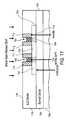
- FIG. 1illustrates a properly-aligned prior art trigate transistor structure 5 comprised of two trigate transistors having respective gates 7 and 8 and a common diffusion region 10 .
- Spacers 1 and 2are adjacent to gate 7 .
- Spacers 3 and 4are adjacent to gate 8 .
- Metallic contacts 21 , 22 , and 23provide electrical contacts to diffusion region 10 .
- Rextexternal electrical resistance
- High external electrical resistancecan occur if metallic contacts are placed at some distance from the gate of a transistor with a thin diffusion body, such as a trigate transistor.
- FIG. 1shows trigate transistor structures 45 with a prior art contact misalignment problem.
- FIG. 3shows transistor structure 45 in cross section. Contacts 31 , 32 , and 33 are misaligned with respect to respective gates 45 and 47 and respective spacers 52 , 53 , 54 , and 55 . A gap between a contact and a spacer (such as gap 42 between contact 32 and spacer 54 ) can result in higher Rext.
- a devicesuch as a static random-access memory (“SRAM”) uses numerous trigate transistors. Misalignment problems with contacts can lead to variations in Rext for the various trigate transistors, however, leading to less predicatability with respect to the design and performance of the overall integrated circuit. This can result in transistor mismatches.
- SRAMstatic random-access memory
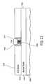
- Diffusion jog 60is an extension of diffusion layer 62 of transistor 64 , which includes gate 66 and spacers 67 and 68 . Diffusion jog 60 serves as a landing pad for contact 70 and thus acts as a contact pad.
- the prior art landing pad approachcan be problematic, however. Due to lithography constraints, the prior art landing pads typically must lie relatively far from the gate of the transistor. The landing pad requires more layout space. The thin silicon body of the diffusion layer and diffusion jog between the contact and the gate typically results in high external electrical resistance. Moreover, the landing pads can create undersirable jogs, sometimes causing problems for optical lithography, especially for sub-100 nanometer (“nm”) devices.
- any transistor with a thin diffusioncan have an Rext problem.
- the thin diffusionwill result from lithography scaling, whether a trigate transistor is used or not. There can be Rext problems even on bulk devices on 65 nanometer nodes.
- FIG. 1shows a layout of a prior art trigate transistor structure with ideal contact placement
- FIG. 2shows a layout of a prior art trigate transistor structure with misaligned contacts
- FIG. 3is a cross section of a prior art trigate transistor structure with misaligned contacts
- FIG. 4shows a layout of a prior art transistor with a landing pad
- FIG. 5is a cross section of a wafer with a transistor structure after metal polish
- FIG. 6is a cross section of the wafer with a photoresist pattern done in preparation for an etch
- FIG. 7is a cross section of the wafer after an etch and after removal of the photoresist
- FIG. 8is a top view of the wafer after the etch, showing the transistor structure
- FIG. 9is a cross section of the wafer after contact metal deposition
- FIG. 10is a cross section of the wafer after planarization
- FIG. 11is a cross section of the wafer after the deposition of an interlayer dielectric and the patterning of contacts;
- FIG. 12is a cross-section of the wafer after the deposition of a first metal layer
- FIG. 13is a layout up to the first metal layer of an SRAM with transistors having self-aligned contacts
- FIGS. 14-16are cross sections of the SRAM of FIG. 13 ;
- FIG. 17is a cross section of a wafer with a transistor structure after a metal gate recess etch
- FIG. 18is a cross section of the wafer after silicon nitride deposition and planarization
- FIG. 19is a cross section of the wafer with protected gates after a self-aligned contact etch and after photoresist removal;
- FIG. 20is a cross section of the wafer with protected gates after contact metal deposition and planarization
- FIG. 21is a cross section of the wafer with protected gates after deposition of a first metal layer
- FIG. 22is a cross section of the wafer with photoresist patterning prior to a gate contact etch
- FIG. 23is a cross section of the wafer after a gate contact etch and after photoresist removal
- FIG. 24is a layout up to the first metal layer of an SRAM with transistors having protected gates and self-aligned contacts;
- FIGS. 25-27are cross sections of the SRAM of FIG. 24 .
- Embodiments of self-aligned contactsare described as well as methods for fabricating such contacts.
- a self-aligned contactbrings the contact physically all the way to a spacer associated with a gate of a transistor.
- This arrangementcan help to minimize electrical external resistance (“Rext”) associated with a thin and long diffusion body of the transistor.
- Rextelectrical external resistance
- the minimization (or elimination) of Rextcan also minimize (or eliminate) variations of Rext. Variations in Rext can cause transistor mismatches.
- superadjacent contactsreside in a layer above the self-aligned contacts and provide respective electrical connections to the self-aligned contacts.
- the self-aligned contactshave a relatively wide top surface layer and the superadjacent contacts have smaller horizontal cross sections than the respective self-aligned contacts. This means that the superadjacent contacts do not have to be precisely aligned with respect to the self-aligned contacts in order to provide proper electrical connections.
- a selective etchis performed. Photoresist is patterned to form an opening above an oxide layer containing one or more transistor gates. Each transistor gate has adjacent spacers. A selective etch is applied from the top of the wafer. The etch acts through the opening in the photoresist to etch the oxide adjacent to the spacers of the gates. The spacers and the gates are not etched by the selective etch. The etch exposes the source and drain regions of a lower diffusion layer. Contact material is deposited to form self-aligned contacts that reside immediately adjacent to the spacers. There are no alignment errors between the contacts and the transistor gate. That is why the self-aligned contacts are referred to as “self-aligned.”
- superadjacent contactsare formed in a layer above the layer containing the self-aligned contacts. Even without being precisely aligned, the superadjacent contact provide electrical connections to the respective self-aligned contacts.
- the self-aligned contact fabrication processcan work with a small diffusion body itself or an epitaxial growth around the small diffusion body of the transistor Because it is difficult to enlarge a small diffusion body with epitaxial growth, a self-aligned contact can provide the benefit of reducing Rext by bringing the contacts to the respective source and drain for either case.
- phase shift maskresults in long lines printing better than small squares.
- a recessis formed at the top of each of the gates. Silicon nitride is deposited in the respective recesses in order to provide protection for the gates. Other embodiments do not employ the gate protection feature.
- FIGS. 5 through 10illustrate process steps for forming self-aligned contacts for transistors.
- the processcan be used for various types of transistors.
- the processis especially beneficial for transistors with an Rext problem.
- Such transistorscan include transistors with a thin diffusion, such as trigate transistors, and even bulk devices on or beyond the 65 nanometer node.
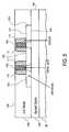
- FIG. 5shows a cross section of a silicon wafer 102 that contains a transistor structure 116 .
- SOIsilicon-on-insulator
- the transistor structure 116is formed with a metal gate process.
- a replacement metal gate processincludes patterning a gate with polysilicon and then etching out the polysilicon gate and replacing it with a metal gate.
- the interlayer dielectric (“ILD”) oxide layer 118is planarized to the top of the metal gates 106 and 108 .
- the planarizationcan stop above the metal gates 106 and 108 .
- the self-aligned contact processis applicable to either the replacement metal gate process or the subtractive metal gate process.
- the ILD layer 118is shown as planarized to the top of the metal gates 106 and 108 .
- the self-aligned contact process describedis applicable to transistors with metal gates, the self-aligned contact process is not restricted to a particular way the metal gates are formed.
- the transistor structure 116includes diffusion layer 104 (also called diffusion body 104 or fin 104 ); gates 106 and 108 ; and spacers 110 , 111 , 112 , and 113 .
- the diffusion layer 104includes drain region 135 and source regions 130 and 131 .
- diffusion layer 104is formed as an SOI structure.
- Buried oxide layer 120is the insulator residing beneath the silicon diffusion layer 104 .
- a silicon substrate 98resides beneath buried oxide layer 120 .
- Gates 106 and 108are each metal gates.
- metal gates 106 and 108are formed after planarization of ILD layer 118 .
- planarization of ILD layer 118is done after formation of gates 106 and 108 .
- Spacers 110 through 113can be made of silicon nitride (“SiN”).
- transistor structure 116After the formation of transistor structure 116 and the planarization of ILD layer 118 , one of two different processing options is used to form self-aligned contacts.
- no gate-protect optionOne option is referred to as the no gate-protect option, which is described below in reference to FIGS. 6 through 16 .
- the no gate-protect optionthere is no additional protection layer formed on gates 106 and 108 .
- the self-aligned contactsimply provides a landing pad for an additional contact layer. After the contact layer is patterned, then an additional metal one layer for the metal lines is patterned, as described in more detail below.
- the second optionis the gate-protection option, which is described with respect to FIGS. 17-27 .
- a recessis formed with respect to each of the gates 106 and 108 .
- Each gate recessis filled with silicon nitride in order to protect the gate.
- a self-aligned contactis formed.
- a metal one layeris then deposited directly above the layer containing the self-aligned contact. Having protection on the gates results in a greater tolerance with respect to alignment errors with respect to the metal one layer. Having protection on the gates also allows smaller spacing between gates, resulting in a more efficient layout.
- FIGS. 6 through 16illustrate the no gate-protection option.
- photoresist 140is spun onto top layer 138 of wafer 102 and ILD oxide layer 118 .
- Photoresist layer 140is then patterned.
- the pattern of photoresist layer 140includes an opening 142 .
- a selective dry etch of oxide against nitrideis applied from the top of wafer 102 to produce a selective etch that removes the ILD oxide material beneath area 142 .
- the etchis selective because spacers 110 through 113 are comprised of silicon nitride which is not etched by the dry etch.
- Such a selective dry etchhas been widely used by the semiconductor industry in sub half-micron technologies.
- Gates 106 and 108are metal gates that are also not etched by the selective etch.
- An aluminum gatefor example, cannot be etched by a fluorine or oxygen based dry etch for silicon oxide.
- opening 142is rectangular and symmetrical with respect to gates 106 and 108 .
- opening 142can have other shapes and need not be symmetrical with respect to gates 106 and 108 .
- opening 142can be circular, square, etc.
- opening 142can be shifted left or right.
- a single gate with spacerscan reside under opening 142 .
- multiple openingsare used for multiple gates with spacers.
- three or more gates with spacerscan reside under a single opening 142 .
- the etchis completed after diffusion layer 116 is exposed for contact.
- the etchremoves part of the top of the exposed diffusion layer 116 in order to maximize the contact area.
- the photoresist layer 140is then removed using known techniques.
- FIG. 7The result is shown in FIG. 7 .
- the selective etchresults in openings 150 , 151 , and 152 down to the diffusion layer 104 .
- Spacers 110 through 113 and gates 108 and 106remain standing, with limited removal of those structures.
- the portions of the ILD oxide layer 118 that resided beneath the photoresist layer 140remain intact.
- openings 150 , 151 , and 152can have various sizes.
- FIG. 8is a top view showing section 160 of wafer 102 and the self-aligned contact etch having openings 150 , 151 , and 152 .
- FIG. 8also shows a top view of transistor structure 116 having diffusion layer 104 , spacers 110 through 113 , and gates 106 and 108 .
- the transistor structure 116includes polysilicon end caps 169 and 171 .
- Polysilicon end cap 169extends from edge 190 of diffusion layer 104 to point 193 .
- the spacer around polysilicon end cap 169extends to point 191 .
- Polysilicon end cap 171extends from edge 195 of diffusion layer 104 to point 198 .
- the spacer around polysilicon end cap 171extends to point 196 .
- Each of the polysilicon end caps 169 and 171needs to be long enough in order to avoid shorts around the respective gates 106 and 108 .
- the self-aligned contact etchcannot be too wide. If the self-aligned contact selective etch is too wide, then the subsequent step of depositing contact metal will result in the contact metal shorting between regions 150 , 151 , and 152 , thereby resulting in improper operation or non-operation of the transistor structure 116 .
- a design ruleis in place for the end caps 169 and 171 such that the end caps 169 and 171 are large enough to accommodate any alignment errors with respect to the self-aligned contact etch.
- the alignment tolerance and spacer thickness associated with a particular technologycan be used in calculating self-aligned contact widths that will not result in shorts.
- One example of a design rule calculation for a 90 nanometer nodeis as follows.
- the alignment tolerance between the self-aligned contact and polyis 60 nanometers.
- the alignment tolerance between poly and diffusionis 60 nanometers.
- the width 178 of the diffusion layer 104is 100 nanometers.
- the poly end cap length “p”must be greater than 75 nm (i.e., p>40 nm+35 nm).
- the design rulestypically follow a 0.7 ⁇ scaling ruler per generation.
- OPCoptical proximity correction
- CDcritical dimension
- OPC methodsthe precise design rules need to be computed with considerations of the critical dimension (“CD”) print bias and the OPC methods. Nevertheless, the method of computation is similar to the one illustrated above.
- FIG. 8also shows (1) contact 164 made to reach gate 106 , (2) contact 166 made to reach gate 108 , and (3) contacts 147 , 148 , and 149 made to reach diffusion layer 104 .
- the metal one layer above transistor structure 116contains metal lines (not shown) above respective contacts 164 , 166 , 147 , 148 , and 149 .
- FIG. 9shows a cross section of wafer 102 with respect to the next operation for the no gate-protect option process.
- a layer 210 of contact metalis deposited on top 138 of ILD oxide layer 118 and fills openings 150 , 151 , and 152 .
- CVDchemical vapor deposition
- ALDatomic layer deposition
- electroplatingelectroless plating
- the contact metal layer 210 of FIG. 9has been polished and planarized to level 137 , which is a level slightly below the original top level 138 of ILD oxide layer 118 and slightly below the original tops of gates 106 and 108 and spacers 110 - 113 .
- level 137need not be perfectly flat and the ILD oxide need not be completely flush with respect to contacts 220 - 222 .
- the result of the planarizationis that contact metal 220 resides in opening 150 , contact metal 221 resides in opening 151 , and contact metal 222 resides in opening 152 .
- contact metals 220 to 222When polished to the targeted level, contact metals 220 to 222 will be isolated from each other by the spacers and gates between the contact metals 220 , 221 , and 222 .
- contact metal 220is isolated from contact metal 221 by gate 106 and spacers 110 and 111 .
- Contact metal 220contacts drain region 130 of diffusion layer 104 .
- Contact metal 222contacts the drain region 131 of diffusion layer 104 .
- Contact metal 221contacts the source region 135 of diffusion layer 104 .
- Contact metal 220reaches the edge of spacer 110 .
- Contact metal 221reaches the respective edges of spacers 111 and 112 .
- Contact metal 222reaches the edge of spacer 113 .
- the contact metal regions 220 , 221 , and 222comprise self-aligned contacts.
- the self-aligned contacts 220 , 221 , and 222provide respective landing pads for a superadjacent contact layer (i.e., a contact layer residing above the self-aligned contacts 220 , 221 , and 222 ), described below.
- the contact metal regions 220 , 221 , and 222provide contact material above the diffusion layer 104 up to the tops of the respective spacers 110 - 113 .
- the superadjacent contacts with respect to the contact metal regions 220 , 221 , and 222do not have to be precisely aligned in order to provide electrical contact.
- the relatively wide top surface areas of self-aligned contacts 220 , 221 , and 222provide sufficient regions for electrical contact to the superadjacent contact layer described below.
- an ILD oxide layer 230is deposited on the top 137 of wafer 102 .
- Photoresistis deposited on the top 265 of the ILD oxide layer 230 .
- the photoresist layeris then patterned to provide openings. Vias 240 , 241 , and 242 are then etched into the ILD oxide layer 230 .
- the photoresistis removed.
- a metal layeris then deposited on the top 265 of wafer 102 , and the metal fills vias 240 , 241 and 242 .
- the metal layer on top of wafer 102is then polished and planarized back to top 265 of wafer 102 .
- metal 250 , 251 , and 252resides in respective vias 240 , 241 , and 242 .
- metal contacts 250 , 251 , and 252are formed.
- Metal contacts 250 , 251 , and 252provide electrical contact to respective self-aligned metallic contacts 220 , 221 , and 222 .
- the self-aligned contacts 220 , 221 , and 222thus provide landing pads for respective contacts 250 , 251 , and 252 .
- contacts 250 , 251 , and 252each have a smaller horizontal surface area than respective self-aligned contacts 220 , 221 , and 222 .
- contacts 250 , 251 , and 252use only a portion of the respective landing pads of self-aligned contacts 220 , 221 , and 222 .
- contacts 250 , 251 , and 252may be rectangular contacts.
- contacts 250 , 251 , and 252are not required as long as contacts 250 , 251 , and 252 contact self-aligned contact landing pads 220 , 221 , and 222 .
- an advantage of this schemeis that self-aligned contacts 220 , 221 , and 222 provide contact to the diffusion layer 104 right up to the edges of respective spacers 110 , 111 , 112 , and 113 .
- Contacts 250 , 251 , and 252merely need to contact respective contacts 220 , 221 , and 222 in order to provide electrical contact right up against respective spacers 110 , 111 , 112 , and 113 .
- FIG. 11shows superadjacent contacts 240 , 241 , and 242 in relatively good alignment with respect to the larger self-aligned contacts 220 , 221 , and 222
- contacts 240 , 241 , and 242can be misaligned with respect to self-aligned contacts 220 , 221 , and 222 as long as there is some metal-to-metal contact that provides an adequate electrical connection between superadjacent contacts 240 , 241 , and 242 and respective self-aligned contacts 220 , 221 , and 222 .
- FIG. 12shows a cross section of wafer 102 after the metal lines 320 , 321 , and 322 are patterned as part of metal one layer 301 using a standard back end process.
- the back end processincludes deposition of ILD oxide layer 300 ; photoresist deposition end patterning; selective etching to form vias 310 , 311 , and 312 ; metal deposition to fill vias 310 , 311 , and 312 ; and planarization.
- Metal lines 320 , 321 , and 322 in respective vias 310 , 311 , and 312provide electrical contact down to diffusion layer 104 via respective contacts 250 , 251 , and 252 and respective self-aligned contacts 220 , 221 , and 222 .
- metal lines 320 and 322provide electrical contact to respective drain regions 130 and 131 .
- Metal line 321provides electrical contact to source region 135 .
- Metal lines 320 , 321 , and 322run to various other transistor structures on wafer 102 .
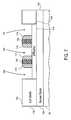
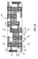
- FIG. 13is a top view of a layout 400 of a static random access memory (“SRAM”) containing transistor structures.
- Layout 400 in FIG. 13shows only one cell.
- the actual cell array for the SRAMhas more cells.
- the SRAMincludes self-aligned contacts with the no gate-protection option.
- the SRAM layout 400is illustrated up through the metal one layer.
- the self-aligned contact openings 406 , 482 , and 510 shown in FIG. 13include the self-aligned contacts.
- Metal one line 440is coupled to Vss.
- Metal one line 442is a node connection.
- Metal one line 502is coupled to a bit line.
- Metal one line 502is coupled to Vcc.
- Gates 441 , 443 , and 504are shown in FIG. 13 .
- FIG. 13also shows contacts 430 , 431 , 432 , 470 , 471 , 520 , and 521 that reside in a layer that lies beneath the metal one layer.
- An N-type metal oxide semiconductor (“NMOS”) diffusion layer 404resides under the self-aligned contact opening 406 .
- An NMOS diffusion layer 480resides under self-aligned contact opening 482 .
- a P-type metal oxide semiconductor (“PMOS”) diffusion layer 500resides under self-aligned contact opening 510 .
- FIGS. 14, 15 , and 16Cross sections of the SRAM layout 400 are shown in FIGS. 14, 15 , and 16 .
- Each of the cross sections shown in FIGS. 14-16is for multiple cells. Thus, each of the cross sections of FIGS. 14-16 extends beyond the one-cell layout 400 shown in FIG. 13 .
- contacts 430 , 431 , 432 , and 433reside within interlayer dielectric oxide layer 408 that is above the self-aligned contacts 416 .
- Metal lines 444 , 442 , 440 , and 423reside in interlayer dielectric oxide layer 410 , which is the metal one layer above layer 408 .
- Bit line 444is superadjacent to and contacts the contact 430 .
- the metal line 442(coupled to a node) resides above and contacts the contact 431 .
- the metal line 440 connected to Vssresides above and contacts the contact 432 .
- the metal line 423acts as a node and resides above and contacts the contact 433 .
- a buried oxide layer 402resides underneath the diffusion layer 404 .
- Silicon substrate 498resides beneath bured oxide layer 402 .
- Gate structures 461 and 464are part of NMOS passivation transistors.
- Gate structures 462 and 463are part of NMOS pull-down transistors.
- Gate structure 460includes gate 450 .
- contacts 470 , 471 , and 472reside above the respective self-aligned contacts 492 .
- the contacts 470 , 471 , and 472reside within vias in interlayer dielectric oxide layer 408 .
- the metal one layer 410comprises metal lines 444 , 442 , 440 , and 423 that reside within the interlayer dielectric oxide layer 410 .
- Metal line 444is coupled to a bit line.
- Metal line 442is a node that resides above and contacts the contact 470 .
- Metal line 440is connected to Vss and resides above and contacts the contact 471 .
- Metal line 423acts as a node and resides above and contacts the contact 472 .
- the buried oxide layer 402resides underneath the NMOS diffusion layer 480 .
- the interlayer dielectric oxide layer 412resides above the buried oxide layer 402 .
- Gate structures 462 and 463(with respective gates 441 and 451 ) are part of NMOS pull-down transistors.
- contacts 520 , 521 , and 522reside above the respective self-aligned contacts 509 , 511 , and 512 .
- Contact 520connects gate 504 (of gate structure 465 ) with self-aligned contact 509 .
- Contact 522connects gate 452 (of gate structure 464 ) with self-aligned contact 512 .
- Contact 521contacts self-aligned contact 511 .
- Gate structures 462 and 463(with respective gates 441 and 451 ) are part of NMOS pull-down transistors.
- the contacts 520 , 521 , and 522reside within the interlayer dielectric oxide layer 408 .
- the metal one layercomprises the interlayer dielectric layer 410 , which includes metal lines 442 , 502 , and 423 .
- the metal line 442acts as a node that resides above and contacts the contact 520 .
- the metal line 502connects with Vss and resides above and contacts the contact 521 .
- the metal line 423acts as a node residing above contact 522 .
- the cell size shown in FIGS. 13 though 16does not assume a spacer process for patterning the diffusion layers.
- Lithographyrequires a minimum space between two self-aligned contacts to be resolved. If the space becomes too small, as feasible with a spacer process, lithography cannot resolve the two self-aligned contact lines. If a spacer process is used to reduce diffusion-to-diffusion space, the self-aligned contact between the two legs of a pull-down device will have to merge. As long as the extension of a self-aligned contact is properly designed, however, as shown by self-aligned contacts 492 of FIG. 15 , there will be no problem with shorting around the gates. In other words, the self-aligned contact should not be too big, but the self-aligned contact should be big enough to tolerate the alignment error and to satisfy the minimum contact area required.
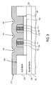
- FIGS. 17 through 23show wafer cross sections that illustrate operations in connection with the gate-protect option with respect to forming self-aligned contacts.
- FIG. 17shows a cross section of wafer 702 that includes a buried oxide layer 720 above a silicon substrate 798 . Buried oxide layer 720 is covered by an interlayer dielectric oxide layer 718 .
- the interlayer dielectric oxide layer 718includes diffusion layer 704 and metal gates 706 and 708 above the diffusion layer 704 .
- Metal gate 706has adjacent spacers 710 and 711 .
- Metal gate 708has adjacent spacers 712 and 713 .
- Diffusion layer 704 , gates 706 and 708 , and spacers 710 though 713form a transistor structure 716 .
- the transistor structure 716includes a pair of transistors with drain regions 730 and 731 and source region 735 .
- a metal gate recess etchis done with a selective etch.
- aluminum gates 706 and 708can be etched using a chlorine dry etch without attacking the silicon oxide of ILD oxide layer 718 .
- the selective etchis needed given that modern transistors typically have a short gate length, which is not possible to align to given the lithography capabilities.
- the recesses 750 and 751 that result from the selective etchare shown in FIG. 17 . If the gate and fill metals are different, then a different dry etch can be used, or a combination of a dry etch and wet etch can be used, to remove metals completely in the open regions 750 and 751 .
- FIG. 18shows a cross section of wafer 702 after the deposition of silicon nitride (“SiN”) in respective regions 750 and 751 , forming caps 760 and 761 over respective metal gates 706 and 708 .
- SiNsilicon nitride
- Silicon nitride caps 760 and 761are formed as follows. A silicon nitride layer is formed over the top 738 of wafer 702 by deposition. The silicon nitride fills openings 750 and 751 , as well as forming a layer over top 738 of wafer 702 . The silicon nitride layer (not shown) is then planarized by polishing the top of wafer 702 . The polishing is done down to the top 738 of wafer 702 . The result is that no silicon nitride is left on the top of wafer 702 except for the silicon nitride caps 760 and 761 filling recesses 750 and 751 over respective metal gates 706 and 708 . The silicon nitride caps 760 and 761 act as protection for respective gates 706 and 708 . For an alternative embodiment, a dry etch may be used for planarization instead of a polish.
- FIG. 19shows a cross section of wafer 702 after a self-aligned contact etch is done from the top of wafer 702 .
- the etchforms open areas 780 , 781 , and 782 adjacent to respective spacers 710 though 713 .
- the self-aligned contact etch used to form open areas 780 though 782 in FIG. 19is similar to the self-aligned contact etch discussed in connection with wafer 102 in FIG. 6 .
- the operations involved in that etchare as follows. A photoresist layer is applied to the top 738 of wafer 702 .
- the photoresist layeris patterned to create an opening above areas 780 , 781 , and 782 , as well as above spacers 710 through 713 and silicon nitride caps 760 and 761 . After the etch, the photoresist layer is removed. The resulting structure is shown in FIG. 19 .
- FIG. 20shows a cross section of wafer 702 after the contact metal has been deposited and planarized to form self-aligned contact areas 820 , 821 , and 822 that provide contact up to the edges of respective spacers 710 , 711 , 712 , and 713 .
- the process for depositing the contact metal to form contact areas 820 , 821 , and 822is similar to the process shown in FIG. 9 .
- a layer of contact metalis deposited on top of surface 738 of wafer 702 .
- the layer of contact metalresides above surface 738 and fills the openings 820 , 821 , and 822 .
- Level 737is a level slightly below the original top level 738 .
- the tops of spacers 710 through 713 and silicon nitride gate caps 760 and 761are not covered by the contact metal after the planarization step is completed.
- the contact metal areas 820 , 821 , and 822are not electrically interconnected with each other.
- Contact metal area 820resides above and contacts the drain region 830 of diffusion layer 704 .
- Contact metal area 822resides above and provides electrical contact to drain region 831 of diffusion area 704 .
- Contact metal area 821resides above and provides electrical contact to source region 835 of diffusion area 704 .
- FIG. 21shows a cross section of wafer 702 with finished self-aligned contacts 820 , 821 , and 822 with a superadjacent metal one layer 930 .
- the metal one layer 930is formed by a metal damanscene process.
- An interlayer dielectric oxide material 931is deposited on top 737 of wafer 702 .
- a photoresist layeris then applied on top 965 of the ILD oxide layer 931 .
- the photoresist layeris patterned to include openings above areas 940 , 941 , and 942 .
- a wet or dry etchis then done from the top to form openings 940 , 941 , and 942 within interlayer dielectric oxide layer 931 .
- the photoresist layeris then removed.
- a metal layeris then deposited on top 965 of wafer 702 .
- the metal layeris comprised of contact metal that covers surface 965 and fills opening 940 , 941 , and 942 .
- the metal layeris then planarized by polishing.
- the metal layeris removed from the top 965 of wafer 702 , but the contact metal remains in openings 940 , 941 , and 942 to form respective metal lines 950 , 951 , and 952 .
- Metal line 950resides on top of self-aligned contact 820 .
- Metal line 950thus provides electrical contact to drain region 830 of diffusion layer 704 .
- Metal line 952resides on top of self-aligned contact 822 .
- Metal line 952provides electrical contact to drain region 831 of diffusion layer 704 .
- Metal line 951resides above self-aligned contact metal 821 .
- Metal line 951provides electrical contact to source region 835 of diffusion region 704 .
- the metal one layer 930which typically has a looser line width control and alignment tolerance than a contact layer—can reside immediately above the self-aligned contacts 820 , 821 , and 822 without the use of an additional contact layer, such as contact layer 230 of FIG. 12 .
- FIGS. 22 and 23show cross sections of semiconductor wafer 1002 in connection with a gate contact patterning process with respect to a gate 1006 that is initially protected by a silicon nitride cap 1060 .
- a gate contactis formed with respect to gate 1006 .
- the gate contact patterning processis done prior to the patterning of self-aligned contacts.
- the gate contact patterningis done after self-aligned contact patterning is completed.
- wafer 1002includes a buried oxide layer 1020 above a silicon substrate 1098 .
- the buried oxide layer 1020resides below an interlayer dielectric oxide layer 1018 .
- the interlayer dielectric oxide layer 1018includes metal gate 1006 with silicon nitride cap 1060 and spacers 1010 and 1011 .
- a photoresist layer 1080is deposited over top 1038 of wafer 1002 .
- the photoresist layer 1080is patterned such that an opening 1082 is formed above silicon nitride cap 1060 and partially above spacers 1010 and 1011 .
- a wet or dry etchis performed from above photoresist layer 1080 .
- the wet or dry etchis resisted by photoresist layer 1080 , but the wet or dry etch acts through opening 1082 to etch away the silicon nitride cap 1060 and portions of the upper regions of spacers 1010 and 1011 .
- the type of wet or dry etch that is performedis one that can remove silicon nitride and that can partially etch away spacers 1010 and 1011 .
- the photoresist layer 1080is then removed after the wet or dry etch.
- the resultis shown in FIG. 23 .
- a notch 1105has been created above metal gate 1006 .
- the opening or notch 1105has been formed through a wet or dry etch by removing the silicon nitride cap 1060 in its entirety and by removing portions of spacers 1010 and 1011 .
- the resultis that the metal gate 1006 is exposed from the top without any protection layer.
- the gate protecthas been removed from gate 1006 .
- the process used to deposit a metal gate contact in notch 1105 of FIG. 23is similar to the metal deposition and planarization processes described above in connection with FIGS. 9 and 20 .
- the formation of a metal gate contact in notch 1105can be done at the same time that metal contacts to a diffusion layer (not shown) are formed for other transistors (not shown) on wafer 1002 .
- the gate contactmay be formed at the same time the metal one layer is formed. This approach can result in a higher aspect ratio for etch and metal deposition.
- a metal one layercan be formed above layer 1018 of silicon wafer 1002 .
- the superadjacent metal one layercan contain metal lines or contacts that contact the metallic gate contact formed within opening 1105 .
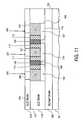
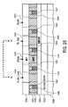
- FIG. 24is a top view of a layout 1400 of an SRAM containing transistor structures with gate-protected self-aligned contacts.
- the SRAM layout 1400is illustrated up through the metal one layer.
- Layout 1400 in FIG. 24shows only one cell.
- the actual cell array for the SRAMhas more cells.
- Cross sections of the SRAM layout 1400are shown in FIGS. 25, 26 , and 27 .
- Each of the cross sections shown in FIGS. 25-27is for multiple cells. Thus, each of the cross sections of FIGS. 25-27 extends beyond the one-cell layout 1400 shown in FIG. 24 .
- the SRAM layoutincludes transistors with self-aligned contact openings 1460 , 1461 and 1462 , which include self-aligned contacts.
- Metal one line 1440is coupled to Vss.
- Metal one line 1442is a node.
- Metal one line 1444is connected to a bit line.
- Metal one line 1445is coupled to Vcc.
- Structures 1441 , 1443 , and 1446are gates.
- An NMOS diffusion area 1504resides under self-aligned contact opening 1460 .
- An NMOS diffusion area 1560resides underneath self-aligned contact opening 1461 .
- a PMOS diffusion arearesides underneath self-aligned contact opening 1462 .
- the self-aligned contacts 1506are immediately above an NMOS layer 1504 .
- the self-aligned contacts 1562are superadjacent to and contact the NMOS layer 1560 .
- the self-aligned contacts 1642are both above and adjacent to the PMOS layer 1600 .
- the NMOS layer 1504resides above the buried oxide layer 1502 .
- Buried oxide layer 1502resides above silicon substrate 1598 .
- Layer 1507includes the self-aligned contacts 1506 and the gate and spacer structures 1550 through 1554 .
- Structures 1550 - 1554include respective gates 1546 , 1443 , 1441 , 1449 , and 1547 .
- Metal one layer 1510resides above layer 1507 and self-aligned contacts 1506 .
- the metal one layerincludes metal lines 1444 , 1442 , 1440 , and 1523 that reside above and contact respective self-aligned contacts of contacts 1506 .
- Metal line 1444is connected to the bit line for the SRAM.
- Metal line 1442is connected to an internal node.
- Metal line 1440is coupled to Vss.
- Metal line 1523is connected to an internal node.
- interlayer dielectric layer 1503resides above buried oxide layer 1502 .
- the interlayer dielectric layer 1503includes gate structures 1552 and 1553 that include respective metal gates 1441 and 1449 with silicon oxide caps and spacers.
- the gate structures 1552 and 1553reside above the NMOS diffusion layer 1560 .
- Self-aligned contacts 1562reside above the NMOS layer 1560 and are adjacent to respective gate structures 1552 and 1553 .
- a metal one layer 1510resides above the interlayer dielectric layer 1503 .
- the metal one layer 1510includes an interlayer dielectric with openings containing metal lines 1444 , 1442 , 1440 , and 1523 .
- Metal line 1444is connected a bit line.
- Metal lines 1442 , 1440 , and 1523reside above and contact respective self-aligned contacts 1562 .
- Metal line 1442is coupled to a node.
- Metal line 1440is coupled to Vss.
- Metal line 1523is coupled to a node. If there were alignment errors, then the metal one layer 1510 could short to the gates of gate structures 1550 - 1554 if those gates were not protected by the silicon nitride caps above those respective gates. In FIG. 26 , however, no alignment error is shown.
- an interlayer dielectric layer 1503resides above the buried oxide layer 1502 .
- the interlayer dielectric layer 1503includes the transistor structure 1616 .
- the transistor structure 1616includes gate structures 1552 and 1590 - 1592 .
- the transistor structurealso includes PMOS layer 1600 and self-aligned contacts 1642 .
- the gate structures 1552 and 1591include spacers along with silicon nitride caps for the respective gates 1441 and 1596 .
- Gate structures 1590 and 1592include respective gates 1446 and 1597 .
- Gate structures 1590 and 1592do not include silicon nitride caps.
- each of the respective self-aligned contacts 1670 and 1671acts as a merged contact that contacts the respective gate as well as the adjacent PMOS diffusion region 1600 .
- contact 1670contacts gate 1446 and PMOS region 1600 .
- Contact 1671contacts gate 1597 and PMOS region 1600 .
- Metal one layer 1510resides immediately above layer 1503 .
- the metal one layer 1510includes an interlayer dielectric that includes openings containing the metal lines 1442 , 1445 , and 1523 .
- Metal lines 1442 , 1445 , and 1523contact respective self-aligned contacts 1642 .
- Metal line 1442is coupled to a node.
- Metal line 1445is coupled to Vcc.
- Metal line 1523is coupled to a node.
- Metal lines 1442 and 1523provide contacts to respective gates 1446 and 1597 .
- Metal line 1445provides electrical contact to the PMOS diffusion layer 1600 via self-aligned contact 1675 .
- Embodiments of the inventionhave been described in detail with respect to transistors on SOI with metal gates.
- a metal gatecan be fabricated from various types of metals, including copper, aluminum, titanium, etc.
- Alternative embodiments of the inventioncan be used with other types of transistors with metal gates, such as trigate transistors and transistors on bulk silicon substrates.
- Embodiments of the inventioncan be used with a transistor having a gate with a protection layer, such as a silicon nitride protection layer. If there is a silicon nitride protective layer, the transistor can have a gate fabricated from various materials, including metal and polysilicon.
- Nanowire devicescan be used with nanowire devices.
- Embodiments of the inventionare applicable to nanowire devices as long as they have a transistor structure with a gate and spacer similar to the silicon transistors described herein.
- the nanowire devicescan be made of various materials, such as silicon or carbon nanotudes.
- Embodiments of the inventioncan involve the fabrication of rectangular self-aligned contacts in the direction of the diffusion region. Shorting is avoided by isolation of the self-aligned contacts through the polishing process.
Landscapes
- Engineering & Computer Science (AREA)
- Physics & Mathematics (AREA)
- Condensed Matter Physics & Semiconductors (AREA)
- General Physics & Mathematics (AREA)
- Manufacturing & Machinery (AREA)
- Computer Hardware Design (AREA)
- Microelectronics & Electronic Packaging (AREA)
- Power Engineering (AREA)
- Internal Circuitry In Semiconductor Integrated Circuit Devices (AREA)
Abstract
Description
- Embodiments of the invention relate to semiconductor layout and fabrication. In particular, embodiments of the invention relate to self-aligned contacts for transistors and methods for fabricating the contacts.
- Trigate transistors and nanowire devices (i.e., transistors having bodies made from nanowires) typically have small geometries. For trigate transistors, the diffusion regions and the gates are typically quite thin.
FIG. 1 illustrates a properly-aligned prior arttrigate transistor structure 5 comprised of two trigate transistors havingrespective gates common diffusion region 10.Spacers gate 7.Spacers gate 8.Metallic contacts diffusion region 10.- One of the problems associated with certain prior art trigate transistors and nanowire devices is that external electrical resistance (“Rext”) can sometimes be relatively high. High external electrical resistance can occur if metallic contacts are placed at some distance from the gate of a transistor with a thin diffusion body, such as a trigate transistor.
- The placement of
contacts FIG. 1 is the goal in the prior art that is not always achieved, given the small geometries and lithography constraints.FIG. 2 showstrigate transistor structures 45 with a prior art contact misalignment problem.FIG. 3 showstransistor structure 45 in cross section.Contacts respective gates respective spacers gap 42 betweencontact 32 and spacer54) can result in higher Rext. - A device such as a static random-access memory (“SRAM”) uses numerous trigate transistors. Misalignment problems with contacts can lead to variations in Rext for the various trigate transistors, however, leading to less predicatability with respect to the design and performance of the overall integrated circuit. This can result in transistor mismatches.
- One approach in the prior art for dealing with the misalignment high Rext problem has been the epitaxial growth of silicon at the source and drain prior to silicide formation in order to help to reduce the external resistance. One problem with that prior art approach, however, is that it is difficult to make a large enough area for a contact using epitaxial growth on a small silicon area—i.e., there is not much silicon to work with.
- Another approach in the prior art for dealing with the misalignment high Rext problem has been to create a silicon diffusion jog to serve as a landing pad, as illustrated in
FIG. 4 .Diffusion jog 60 is an extension ofdiffusion layer 62 oftransistor 64, which includesgate 66 andspacers Diffusion jog 60 serves as a landing pad forcontact 70 and thus acts as a contact pad. - The prior art landing pad approach can be problematic, however. Due to lithography constraints, the prior art landing pads typically must lie relatively far from the gate of the transistor. The landing pad requires more layout space. The thin silicon body of the diffusion layer and diffusion jog between the contact and the gate typically results in high external electrical resistance. Moreover, the landing pads can create undersirable jogs, sometimes causing problems for optical lithography, especially for sub-100 nanometer (“nm”) devices.
- External electrical resistance problems can occur on devices beside trigate transistors. In principle, any transistor with a thin diffusion can have an Rext problem. The thin diffusion will result from lithography scaling, whether a trigate transistor is used or not. There can be Rext problems even on bulk devices on 65 nanometer nodes.
- In the prior art, printing a rectangular contact in the diffusion direction sometimes can short the diffusion to the gate. Printing a rectangular contact in the direction perpendicular to the diffusion region can require more layout space.
- Embodiments of the present invention are illustrated by way of example and not limitation in the figures of the accompanying drawings, in which like references indicate similar elements and in which:
FIG. 1 shows a layout of a prior art trigate transistor structure with ideal contact placement;FIG. 2 shows a layout of a prior art trigate transistor structure with misaligned contacts;FIG. 3 is a cross section of a prior art trigate transistor structure with misaligned contacts;FIG. 4 shows a layout of a prior art transistor with a landing pad;FIG. 5 is a cross section of a wafer with a transistor structure after metal polish;FIG. 6 is a cross section of the wafer with a photoresist pattern done in preparation for an etch;FIG. 7 is a cross section of the wafer after an etch and after removal of the photoresist;FIG. 8 is a top view of the wafer after the etch, showing the transistor structure;FIG. 9 is a cross section of the wafer after contact metal deposition;FIG. 10 is a cross section of the wafer after planarization;FIG. 11 is a cross section of the wafer after the deposition of an interlayer dielectric and the patterning of contacts;FIG. 12 is a cross-section of the wafer after the deposition of a first metal layer;FIG. 13 is a layout up to the first metal layer of an SRAM with transistors having self-aligned contacts;FIGS. 14-16 are cross sections of the SRAM ofFIG. 13 ;FIG. 17 is a cross section of a wafer with a transistor structure after a metal gate recess etch;FIG. 18 is a cross section of the wafer after silicon nitride deposition and planarization;FIG. 19 is a cross section of the wafer with protected gates after a self-aligned contact etch and after photoresist removal;FIG. 20 is a cross section of the wafer with protected gates after contact metal deposition and planarization;FIG. 21 is a cross section of the wafer with protected gates after deposition of a first metal layer;FIG. 22 is a cross section of the wafer with photoresist patterning prior to a gate contact etch;FIG. 23 is a cross section of the wafer after a gate contact etch and after photoresist removal;FIG. 24 is a layout up to the first metal layer of an SRAM with transistors having protected gates and self-aligned contacts;FIGS. 25-27 are cross sections of the SRAM ofFIG. 24 .- Embodiments of self-aligned contacts are described as well as methods for fabricating such contacts.
- As described in more detail below, a self-aligned contact (“SAC”) brings the contact physically all the way to a spacer associated with a gate of a transistor. This arrangement can help to minimize electrical external resistance (“Rext”) associated with a thin and long diffusion body of the transistor. The minimization (or elimination) of Rext can also minimize (or eliminate) variations of Rext. Variations in Rext can cause transistor mismatches.
- For one embodiment, superadjacent contacts reside in a layer above the self-aligned contacts and provide respective electrical connections to the self-aligned contacts. The self-aligned contacts have a relatively wide top surface layer and the superadjacent contacts have smaller horizontal cross sections than the respective self-aligned contacts. This means that the superadjacent contacts do not have to be precisely aligned with respect to the self-aligned contacts in order to provide proper electrical connections.
- In order to form self-aligned contacts, a selective etch is performed. Photoresist is patterned to form an opening above an oxide layer containing one or more transistor gates. Each transistor gate has adjacent spacers. A selective etch is applied from the top of the wafer. The etch acts through the opening in the photoresist to etch the oxide adjacent to the spacers of the gates. The spacers and the gates are not etched by the selective etch. The etch exposes the source and drain regions of a lower diffusion layer. Contact material is deposited to form self-aligned contacts that reside immediately adjacent to the spacers. There are no alignment errors between the contacts and the transistor gate. That is why the self-aligned contacts are referred to as “self-aligned.”
- For one embodiment, superadjacent contacts are formed in a layer above the layer containing the self-aligned contacts. Even without being precisely aligned, the superadjacent contact provide electrical connections to the respective self-aligned contacts.
- Instead of having to grow a large area for a landing pad, the self-aligned contact fabrication process can work with a small diffusion body itself or an epitaxial growth around the small diffusion body of the transistor Because it is difficult to enlarge a small diffusion body with epitaxial growth, a self-aligned contact can provide the benefit of reducing Rext by bringing the contacts to the respective source and drain for either case.
- Moreover, the use of self-aligned contacts allows the printing of rectangular contacts, which may help to minimize a contact printing problem related to phase shift mask. Phase shift mask results in long lines printing better than small squares.
- For one embodiment, a recess is formed at the top of each of the gates. Silicon nitride is deposited in the respective recesses in order to provide protection for the gates. Other embodiments do not employ the gate protection feature.
- As described in more detail below, well-established silicon processes can be used as part of the self-aligned contact fabrication processes of embodiments of the invention.
FIGS. 5 through 10 illustrate process steps for forming self-aligned contacts for transistors. The process can be used for various types of transistors. The process is especially beneficial for transistors with an Rext problem. Such transistors can include transistors with a thin diffusion, such as trigate transistors, and even bulk devices on or beyond the 65 nanometer node.FIG. 5 shows a cross section of asilicon wafer 102 that contains atransistor structure 116. Although a silicon-on-insulator (“SOI”) substrate is illustrated, the process is applicable to transistors on bulk substrates. Thetransistor structure 116 is formed with a metal gate process. A replacement metal gate process includes patterning a gate with polysilicon and then etching out the polysilicon gate and replacing it with a metal gate. For a replacement metal gate process, the interlayer dielectric (“ILD”)oxide layer 118 is planarized to the top of themetal gates metal gates FIGS. 5 and 6 , theILD layer 118 is shown as planarized to the top of themetal gates - Although the self-aligned contact process described is applicable to transistors with metal gates, the self-aligned contact process is not restricted to a particular way the metal gates are formed.
- The
transistor structure 116 includes diffusion layer104 (also calleddiffusion body 104 or fin104);gates spacers diffusion layer 104 includesdrain region 135 andsource regions - For one embodiment,
diffusion layer 104 is formed as an SOI structure.Buried oxide layer 120 is the insulator residing beneath thesilicon diffusion layer 104. Asilicon substrate 98 resides beneath buriedoxide layer 120.Gates metal gates ILD layer 118. For a subtractive metal gate process, planarization ofILD layer 118 is done after formation ofgates Spacers 110 through113 can be made of silicon nitride (“SiN”). - After the formation of
transistor structure 116 and the planarization ofILD layer 118, one of two different processing options is used to form self-aligned contacts. - One option is referred to as the no gate-protect option, which is described below in reference to
FIGS. 6 through 16 . For the no gate-protect option, there is no additional protection layer formed ongates - The second option is the gate-protection option, which is described with respect to
FIGS. 17-27 . For the gate-protection option, a recess is formed with respect to each of thegates FIGS. 6 through 16 illustrate the no gate-protection option. As shown inFIG. 6 ,photoresist 140 is spun ontotop layer 138 ofwafer 102 andILD oxide layer 118.Photoresist layer 140 is then patterned. The pattern ofphotoresist layer 140 includes anopening 142. A selective dry etch of oxide against nitride is applied from the top ofwafer 102 to produce a selective etch that removes the ILD oxide material beneatharea 142. The etch is selective becausespacers 110 through113 are comprised of silicon nitride which is not etched by the dry etch. Such a selective dry etch has been widely used by the semiconductor industry in sub half-micron technologies.Gates - For one embodiment, opening142 is rectangular and symmetrical with respect to
gates gates - For one alternative embodiment, a single gate with spacers can reside under
opening 142. For alternative embodiments, multiple openings are used for multiple gates with spacers. For other alternative embodiments, three or more gates with spacers can reside under asingle opening 142. - The etch is completed after
diffusion layer 116 is exposed for contact. For one embodiment, the etch removes part of the top of the exposeddiffusion layer 116 in order to maximize the contact area. Thephotoresist layer 140 is then removed using known techniques. - The result is shown in
FIG. 7 . The selective etch results inopenings diffusion layer 104.Spacers 110 through113 andgates ILD oxide layer 118 that resided beneath thephotoresist layer 140 remain intact. - For alternative embodiments,
openings FIG. 8 is a topview showing section 160 ofwafer 102 and the self-aligned contactetch having openings FIG. 8 also shows a top view oftransistor structure 116 havingdiffusion layer 104,spacers 110 through113, andgates - The
transistor structure 116 includes polysilicon end caps169 and171.Polysilicon end cap 169 extends fromedge 190 ofdiffusion layer 104 to point193. The spacer aroundpolysilicon end cap 169 extends to point191.Polysilicon end cap 171 extends fromedge 195 ofdiffusion layer 104 to point198. The spacer aroundpolysilicon end cap 171 extends to point196. - Each of the polysilicon end caps169 and171 needs to be long enough in order to avoid shorts around the
respective gates regions transistor structure 116. - For one embodiment, a design rule is in place for the end caps169 and171 such that the end caps169 and171 are large enough to accommodate any alignment errors with respect to the self-aligned contact etch. The alignment tolerance and spacer thickness associated with a particular technology can be used in calculating self-aligned contact widths that will not result in shorts. One example of a design rule calculation for a 90 nanometer node is as follows. The alignment tolerance between the self-aligned contact and poly is 60 nanometers. The alignment tolerance between poly and diffusion is 60 nanometers. The
width 178 of thediffusion layer 104 is 100 nanometers. The 100 nm diffusion is smaller than a typical 90 nm design rule at 140 nm, but is chosen here to illustrate the advantages of self-aligned contacts. Because poly is aligned to diffusion, the alignment between a self-aligned contact and the diffusion is equal to the square root of thesum 602+602, or 85 nm. To ensure a minimum of 40 nanometer coverage on a 100 nanometer wide diffusion, such asdiffusion layer 104, the self-aligned contact opening needs to extend beyond eachdiffusion edge distances width 174 of the self-alignedcontact 150 is 150 nm (i.e., 25 nm+100 nm+25 nm=150 nm), which is readily patterned in a 90 nm mode. If the difference is wider than 100 nm, the overlap will be larger. - The misalignment of a self-aligned contact can result in a worst case wherein an edge of self-aligned
contact 151 is located relative to edge191 of the spacer at a distance X=(25+60−p−50) nm, wherein 25 nm is the distance from anedge 153 of self-alignedcontact 151 todiffusion edge poly end cap 169 from190 to193, and 50 nm is assumed to be the spacer thickness from193 to191. If “X” is greater than zero, then theedge 153 of self-alignedcontact 151 would be located beyond thespacer edge 191 and thecontacts gate 106. - To ensure proper isolation, assuming a margin of 40 nm, the poly end cap length “p” must be greater than 75 nm (i.e., p>40 nm+35 nm). The poly end cap for 90 nm is set at 100 nm to allow a 40 nm margin on top of the alignment tolerance (i.e., 100 nm=60 nm+40 nm). Therefore, the typical design rule for the poly end cap, such as
poly end cap 169, is sufficient to ensure that the self-aligned contacts (such ascontacts 150 and151) do not short around the gate, such as gate106 (i.e., 100 nm>75 nm). - For sub-100 nm lithography, the design rules typically follow a 0.7× scaling ruler per generation. When techniques such as optical proximity correction (“OPC”) are employed, the precise design rules need to be computed with considerations of the critical dimension (“CD”) print bias and the OPC methods. Nevertheless, the method of computation is similar to the one illustrated above.
- There is no impact on the layout area as a result of the self-aligned contact etch with the no gate-protect option. A self-aligned contact etch using the gate-protect option allows a smaller layout area.
FIG. 8 also shows (1) contact164 made to reachgate 106, (2) contact166 made to reachgate 108, and (3)contacts diffusion layer 104. The metal one layer abovetransistor structure 116 contains metal lines (not shown) aboverespective contacts FIG. 9 shows a cross section ofwafer 102 with respect to the next operation for the no gate-protect option process. Alayer 210 of contact metal is deposited ontop 138 ofILD oxide layer 118 and fillsopenings - For certain embodiments, chemical vapor deposition (“CVD”) or atomic layer deposition (“ALD”) can be used to form
layer 210. Alternatively, other techniques, such as electroplating or electroless plating, can be used. - As shown in
FIG. 10 , thecontact metal layer 210 ofFIG. 9 has been polished and planarized tolevel 137, which is a level slightly below theoriginal top level 138 ofILD oxide layer 118 and slightly below the original tops ofgates level 137 need not be perfectly flat and the ILD oxide need not be completely flush with respect to contacts220-222. The result of the planarization is thatcontact metal 220 resides inopening 150,contact metal 221 resides inopening 151, andcontact metal 222 resides inopening 152. When polished to the targeted level,contact metals 220 to222 will be isolated from each other by the spacers and gates between thecontact metals contact metal 220 is isolated fromcontact metal 221 bygate 106 andspacers Contact metal 220 contacts drainregion 130 ofdiffusion layer 104.Contact metal 222 contacts thedrain region 131 ofdiffusion layer 104.Contact metal 221 contacts thesource region 135 ofdiffusion layer 104.Contact metal 220 reaches the edge ofspacer 110.Contact metal 221 reaches the respective edges ofspacers Contact metal 222 reaches the edge ofspacer 113.- The
contact metal regions contacts contacts contact metal regions diffusion layer 104 up to the tops of the respective spacers110-113. - The superadjacent contacts with respect to the
contact metal regions contacts - As shown in
FIG. 11 , anILD oxide layer 230 is deposited on the top137 ofwafer 102. Photoresist is deposited on the top265 of theILD oxide layer 230. The photoresist layer is then patterned to provide openings.Vias ILD oxide layer 230. The photoresist is removed. A metal layer is then deposited on the top265 ofwafer 102, and the metal fillsvias wafer 102 is then polished and planarized back totop 265 ofwafer 102. The result is thatmetal respective vias metal contacts Metal contacts metallic contacts contacts respective contacts contacts contacts contacts contacts contacts - The precise location of
contacts contacts contact landing pads contacts diffusion layer 104 right up to the edges ofrespective spacers Contacts respective contacts respective spacers - Although
FIG. 11 shows superadjacentcontacts contacts other embodiments contacts contacts superadjacent contacts contacts FIG. 12 shows a cross section ofwafer 102 after themetal lines layer 301 using a standard back end process.- The back end process includes deposition of
ILD oxide layer 300; photoresist deposition end patterning; selective etching to form vias310,311, and312; metal deposition to fillvias Metal lines respective vias diffusion layer 104 viarespective contacts contacts metal lines respective drain regions Metal line 321 provides electrical contact to sourceregion 135.Metal lines wafer 102. FIG. 13 is a top view of alayout 400 of a static random access memory (“SRAM”) containing transistor structures.Layout 400 inFIG. 13 shows only one cell. The actual cell array for the SRAM has more cells. The SRAM includes self-aligned contacts with the no gate-protection option. TheSRAM layout 400 is illustrated up through the metal one layer.- The self-aligned
contact openings FIG. 13 include the self-aligned contacts. Metal oneline 440 is coupled to Vss. Metal oneline 442 is a node connection. Metal oneline 502 is coupled to a bit line. Metal oneline 502 is coupled to Vcc.Gates FIG. 13 .FIG. 13 also showscontacts diffusion layer 404 resides under the self-alignedcontact opening 406. AnNMOS diffusion layer 480 resides under self-alignedcontact opening 482. A P-type metal oxide semiconductor (“PMOS”)diffusion layer 500 resides under self-alignedcontact opening 510. - Cross sections of the
SRAM layout 400 are shown inFIGS. 14, 15 , and16. Each of the cross sections shown inFIGS. 14-16 is for multiple cells. Thus, each of the cross sections ofFIGS. 14-16 extends beyond the one-cell layout 400 shown inFIG. 13 . - As shown in
FIG. 14 ,contacts dielectric oxide layer 408 that is above the self-alignedcontacts 416.Metal lines dielectric oxide layer 410, which is the metal one layer abovelayer 408.Bit line 444 is superadjacent to and contacts thecontact 430. The metal line442 (coupled to a node) resides above and contacts thecontact 431. Themetal line 440 connected to Vss resides above and contacts thecontact 432. Themetal line 423 acts as a node and resides above and contacts thecontact 433. - A buried
oxide layer 402 resides underneath thediffusion layer 404.Silicon substrate 498 resides beneathbured oxide layer 402.Gate structures 461 and464 (withrespective gates 443 and452) are part of NMOS passivation transistors.Gate structures 462 and463 (withrespective gates 441 and451) are part of NMOS pull-down transistors.Gate structure 460 includesgate 450. - As shown in
FIG. 15 ,contacts contacts 492. Thecontacts dielectric oxide layer 408. The metal onelayer 410 comprisesmetal lines dielectric oxide layer 410.Metal line 444 is coupled to a bit line.Metal line 442 is a node that resides above and contacts thecontact 470.Metal line 440 is connected to Vss and resides above and contacts thecontact 471.Metal line 423 acts as a node and resides above and contacts thecontact 472. - The buried
oxide layer 402 resides underneath theNMOS diffusion layer 480. The interlayerdielectric oxide layer 412 resides above the buriedoxide layer 402.Gate structures 462 and463 (withrespective gates 441 and451) are part of NMOS pull-down transistors. - As shown in
FIG. 16 ,contacts contacts contact 509. Contact522 connects gate452 (of gate structure464) with self-alignedcontact 512. Contact521 contacts self-alignedcontact 511.Gate structures 462 and463 (withrespective gates 441 and451) are part of NMOS pull-down transistors. Thecontacts dielectric oxide layer 408. - The metal one layer comprises the
interlayer dielectric layer 410, which includesmetal lines metal line 442 acts as a node that resides above and contacts thecontact 520. Themetal line 502 connects with Vss and resides above and contacts thecontact 521. Themetal line 423 acts as a node residing abovecontact 522. - The cell size shown in FIGS.13 though16 does not assume a spacer process for patterning the diffusion layers. Lithography requires a minimum space between two self-aligned contacts to be resolved. If the space becomes too small, as feasible with a spacer process, lithography cannot resolve the two self-aligned contact lines. If a spacer process is used to reduce diffusion-to-diffusion space, the self-aligned contact between the two legs of a pull-down device will have to merge. As long as the extension of a self-aligned contact is properly designed, however, as shown by self-aligned
contacts 492 ofFIG. 15 , there will be no problem with shorting around the gates. In other words, the self-aligned contact should not be too big, but the self-aligned contact should be big enough to tolerate the alignment error and to satisfy the minimum contact area required. FIGS. 17 through 23 show wafer cross sections that illustrate operations in connection with the gate-protect option with respect to forming self-aligned contacts.FIG. 17 shows a cross section ofwafer 702 that includes a buriedoxide layer 720 above asilicon substrate 798.Buried oxide layer 720 is covered by an interlayerdielectric oxide layer 718. The interlayerdielectric oxide layer 718 includesdiffusion layer 704 andmetal gates diffusion layer 704.Metal gate 706 hasadjacent spacers Metal gate 708 hasadjacent spacers Diffusion layer 704,gates spacers 710 though713 form atransistor structure 716. Thetransistor structure 716 includes a pair of transistors withdrain regions 730 and731 andsource region 735.- The gate-protect operations begin as follows. A metal gate recess etch is done with a selective etch. For example,
aluminum gates ILD oxide layer 718. The selective etch is needed given that modern transistors typically have a short gate length, which is not possible to align to given the lithography capabilities. Therecesses FIG. 17 . If the gate and fill metals are different, then a different dry etch can be used, or a combination of a dry etch and wet etch can be used, to remove metals completely in theopen regions FIG. 18 shows a cross section ofwafer 702 after the deposition of silicon nitride (“SiN”) inrespective regions caps respective metal gates - Silicon nitride caps760 and761 are formed as follows. A silicon nitride layer is formed over the top738 of
wafer 702 by deposition. The silicon nitride fillsopenings top 738 ofwafer 702. The silicon nitride layer (not shown) is then planarized by polishing the top ofwafer 702. The polishing is done down to the top738 ofwafer 702. The result is that no silicon nitride is left on the top ofwafer 702 except for the silicon nitride caps760 and761 fillingrecesses respective metal gates respective gates FIG. 19 shows a cross section ofwafer 702 after a self-aligned contact etch is done from the top ofwafer 702. The etch formsopen areas respective spacers 710 though713. The self-aligned contact etch used to formopen areas 780 though782 inFIG. 19 is similar to the self-aligned contact etch discussed in connection withwafer 102 inFIG. 6 . The operations involved in that etch are as follows. A photoresist layer is applied to the top738 ofwafer 702. The photoresist layer is patterned to create an opening aboveareas above spacers 710 through713 and silicon nitride caps760 and761. After the etch, the photoresist layer is removed. The resulting structure is shown inFIG. 19 .FIG. 20 shows a cross section ofwafer 702 after the contact metal has been deposited and planarized to form self-alignedcontact areas respective spacers - The process for depositing the contact metal to form
contact areas FIG. 9 . Although not shown inFIG. 20 , a layer of contact metal is deposited on top ofsurface 738 ofwafer 702. The layer of contact metal resides abovesurface 738 and fills theopenings level 737 in order to formcontact areas Level 737 is a level slightly below theoriginal top level 738. The tops ofspacers 710 through713 and silicon nitride gate caps760 and761 are not covered by the contact metal after the planarization step is completed. Thus, thecontact metal areas - Contact
metal area 820 resides above and contacts thedrain region 830 ofdiffusion layer 704. Contactmetal area 822 resides above and provides electrical contact to drainregion 831 ofdiffusion area 704. Contactmetal area 821 resides above and provides electrical contact to sourceregion 835 ofdiffusion area 704. FIG. 21 shows a cross section ofwafer 702 with finished self-alignedcontacts layer 930. The metal onelayer 930 is formed by a metal damanscene process. An interlayerdielectric oxide material 931 is deposited ontop 737 ofwafer 702. A photoresist layer is then applied ontop 965 of theILD oxide layer 931. The photoresist layer is patterned to include openings aboveareas openings dielectric oxide layer 931. The photoresist layer is then removed. A metal layer is then deposited ontop 965 ofwafer 702. The metal layer is comprised of contact metal that coverssurface 965 and fills opening940,941, and942. The metal layer is then planarized by polishing. The metal layer is removed from the top965 ofwafer 702, but the contact metal remains inopenings respective metal lines Metal line 950 resides on top of self-alignedcontact 820.Metal line 950 thus provides electrical contact to drainregion 830 ofdiffusion layer 704.Metal line 952 resides on top of self-alignedcontact 822.Metal line 952 provides electrical contact to drainregion 831 ofdiffusion layer 704.Metal line 951 resides above self-alignedcontact metal 821.Metal line 951 provides electrical contact to sourceregion 835 ofdiffusion region 704.- Because the
metal gates layer 930—which typically has a looser line width control and alignment tolerance than a contact layer—can reside immediately above the self-alignedcontacts contact layer 230 ofFIG. 12 . FIGS. 22 and 23 show cross sections ofsemiconductor wafer 1002 in connection with a gate contact patterning process with respect to agate 1006 that is initially protected by asilicon nitride cap 1060. In other words, a gate contact is formed with respect togate 1006. For the embodiment shown inFIGS. 22 and 23 , the gate contact patterning process is done prior to the patterning of self-aligned contacts. For another embodiment, the gate contact patterning is done after self-aligned contact patterning is completed.- As shown in
FIG. 22 ,wafer 1002 includes a buriedoxide layer 1020 above asilicon substrate 1098. The buriedoxide layer 1020 resides below an interlayerdielectric oxide layer 1018. The interlayerdielectric oxide layer 1018 includesmetal gate 1006 withsilicon nitride cap 1060 andspacers - A
photoresist layer 1080 is deposited over top1038 ofwafer 1002. Thephotoresist layer 1080 is patterned such that anopening 1082 is formed abovesilicon nitride cap 1060 and partially abovespacers - A wet or dry etch is performed from above
photoresist layer 1080. The wet or dry etch is resisted byphotoresist layer 1080, but the wet or dry etch acts throughopening 1082 to etch away thesilicon nitride cap 1060 and portions of the upper regions ofspacers spacers - The
photoresist layer 1080 is then removed after the wet or dry etch. The result is shown inFIG. 23 . Anotch 1105 has been created abovemetal gate 1006. The opening ornotch 1105 has been formed through a wet or dry etch by removing thesilicon nitride cap 1060 in its entirety and by removing portions ofspacers metal gate 1006 is exposed from the top without any protection layer. Thus, the gate protect has been removed fromgate 1006. - The process used to deposit a metal gate contact in
notch 1105 ofFIG. 23 is similar to the metal deposition and planarization processes described above in connection withFIGS. 9 and 20 . The formation of a metal gate contact innotch 1105 can be done at the same time that metal contacts to a diffusion layer (not shown) are formed for other transistors (not shown) onwafer 1002. Alternatively, the gate contact may be formed at the same time the metal one layer is formed. This approach can result in a higher aspect ratio for etch and metal deposition. - In subsequent processing operations, a metal one layer can be formed above
layer 1018 ofsilicon wafer 1002. The superadjacent metal one layer can contain metal lines or contacts that contact the metallic gate contact formed withinopening 1105. FIG. 24 is a top view of alayout 1400 of an SRAM containing transistor structures with gate-protected self-aligned contacts. TheSRAM layout 1400 is illustrated up through the metal one layer.Layout 1400 inFIG. 24 shows only one cell. The actual cell array for the SRAM has more cells. Cross sections of theSRAM layout 1400 are shown inFIGS. 25, 26 , and27. Each of the cross sections shown inFIGS. 25-27 is for multiple cells. Thus, each of the cross sections ofFIGS. 25-27 extends beyond the one-cell layout 1400 shown inFIG. 24 .- The SRAM layout includes transistors with self-aligned
contact openings line 1440 is coupled to Vss. Metal oneline 1442 is a node. Metal oneline 1444 is connected to a bit line. Metal oneline 1445 is coupled to Vcc.Structures NMOS diffusion area 1504 resides under self-alignedcontact opening 1460. AnNMOS diffusion area 1560 resides underneath self-alignedcontact opening 1461. A PMOS diffusion area resides underneath self-alignedcontact opening 1462. - As shown in
FIG. 25 , the self-alignedcontacts 1506 are immediately above anNMOS layer 1504. As shown inFIG. 26 , the self-alignedcontacts 1562 are superadjacent to and contact theNMOS layer 1560. As shown inFIG. 27 , the self-alignedcontacts 1642 are both above and adjacent to thePMOS layer 1600. - As shown in
FIG. 25 , theNMOS layer 1504 resides above the buriedoxide layer 1502.Buried oxide layer 1502 resides abovesilicon substrate 1598.Layer 1507 includes the self-alignedcontacts 1506 and the gate andspacer structures 1550 through1554. Structures1550-1554 includerespective gates layer 1510 resides abovelayer 1507 and self-alignedcontacts 1506. The metal one layer includesmetal lines contacts 1506.Metal line 1444 is connected to the bit line for the SRAM.Metal line 1442 is connected to an internal node.Metal line 1440 is coupled to Vss.Metal line 1523 is connected to an internal node. - As shown in
FIG. 26 ,interlayer dielectric layer 1503 resides above buriedoxide layer 1502. Theinterlayer dielectric layer 1503 includesgate structures respective metal gates gate structures NMOS diffusion layer 1560. Self-alignedcontacts 1562 reside above theNMOS layer 1560 and are adjacent torespective gate structures layer 1510 resides above theinterlayer dielectric layer 1503. The metal onelayer 1510 includes an interlayer dielectric with openings containingmetal lines Metal line 1444 is connected a bit line.Metal lines contacts 1562.Metal line 1442 is coupled to a node.Metal line 1440 is coupled to Vss.Metal line 1523 is coupled to a node. If there were alignment errors, then the metal onelayer 1510 could short to the gates of gate structures1550-1554 if those gates were not protected by the silicon nitride caps above those respective gates. InFIG. 26 , however, no alignment error is shown. - As shown in
FIG. 27 , aninterlayer dielectric layer 1503 resides above the buriedoxide layer 1502. Theinterlayer dielectric layer 1503 includes thetransistor structure 1616. Thetransistor structure 1616 includesgate structures 1552 and1590-1592. The transistor structure also includesPMOS layer 1600 and self-alignedcontacts 1642. Thegate structures respective gates Gate structures respective gates Gate structures gate structures contacts PMOS diffusion region 1600. Thus, contact1670contacts gate 1446 andPMOS region 1600.Contact 1671contacts gate 1597 andPMOS region 1600. - Metal one
layer 1510 resides immediately abovelayer 1503. The metal onelayer 1510 includes an interlayer dielectric that includes openings containing themetal lines Metal lines contacts 1642.Metal line 1442 is coupled to a node.Metal line 1445 is coupled to Vcc.Metal line 1523 is coupled to a node.Metal lines respective gates Metal line 1445 provides electrical contact to thePMOS diffusion layer 1600 via self-alignedcontact 1675. - Embodiments of the invention have been described in detail with respect to transistors on SOI with metal gates. A metal gate can be fabricated from various types of metals, including copper, aluminum, titanium, etc. Alternative embodiments of the invention can be used with other types of transistors with metal gates, such as trigate transistors and transistors on bulk silicon substrates. Embodiments of the invention can be used with a transistor having a gate with a protection layer, such as a silicon nitride protection layer. If there is a silicon nitride protective layer, the transistor can have a gate fabricated from various materials, including metal and polysilicon.
- Alternative embodiments of the invention can be used with nanowire devices. Embodiments of the invention are applicable to nanowire devices as long as they have a transistor structure with a gate and spacer similar to the silicon transistors described herein. The nanowire devices can be made of various materials, such as silicon or carbon nanotudes.
- Embodiments of the invention can involve the fabrication of rectangular self-aligned contacts in the direction of the diffusion region. Shorting is avoided by isolation of the self-aligned contacts through the polishing process.
- In the foregoing specification, specific exemplary embodiments of the invention have been described. It will, however, be evident that various modifications and changes may be made thereto. The specification and drawings are, accordingly, to be regarded in an illustrative rather than a restrictive sense.
Claims (25)
Priority Applications (1)
| Application Number | Priority Date | Filing Date | Title |
|---|---|---|---|
| US11/097,429US7563701B2 (en) | 2005-03-31 | 2005-03-31 | Self-aligned contacts for transistors |
Applications Claiming Priority (1)
| Application Number | Priority Date | Filing Date | Title |
|---|---|---|---|
| US11/097,429US7563701B2 (en) | 2005-03-31 | 2005-03-31 | Self-aligned contacts for transistors |
Publications (2)
| Publication Number | Publication Date |
|---|---|
| US20060223302A1true US20060223302A1 (en) | 2006-10-05 |
| US7563701B2 US7563701B2 (en) | 2009-07-21 |
Family
ID=37071121
Family Applications (1)
| Application Number | Title | Priority Date | Filing Date |
|---|---|---|---|
| US11/097,429Active2026-02-26US7563701B2 (en) | 2005-03-31 | 2005-03-31 | Self-aligned contacts for transistors |
Country Status (1)
| Country | Link |
|---|---|
| US (1) | US7563701B2 (en) |
Cited By (77)
| Publication number | Priority date | Publication date | Assignee | Title |
|---|---|---|---|---|
| US20080120588A1 (en)* | 2005-06-27 | 2008-05-22 | Becker Scott T | Methods for Creating Primitive Constructed Standard Cells |
| US7446352B2 (en) | 2006-03-09 | 2008-11-04 | Tela Innovations, Inc. | Dynamic array architecture |
| US20090004857A1 (en)* | 2007-06-29 | 2009-01-01 | Chikarmane Vinay B | Method of manufacturing a semiconductor device using the self aligned contact (SAC) process flow for semiconductor devices with aluminum metal gates |
| US20090037864A1 (en)* | 2007-08-02 | 2009-02-05 | Tela Innovations, Inc. | Methods for Designing Semiconductor Device with Dynamic Array Section |
| US20090080244A1 (en)* | 2007-09-17 | 2009-03-26 | Eric Carman | Refreshing Data of Memory Cells with Electrically Floating Body Transistors |
| US20090108360A1 (en)* | 2007-10-26 | 2009-04-30 | Tela Innovations, Inc. | Methods, structures and designs for self-aligning local interconnects used in integrated circuits |
| US7577049B1 (en) | 2006-08-08 | 2009-08-18 | Tela Innovations, Inc. | Speculative sense enable tuning apparatus and associated methods |
| US7590968B1 (en) | 2006-03-01 | 2009-09-15 | Tela Innovations, Inc. | Methods for risk-informed chip layout generation |
| US20100006951A1 (en)* | 2006-03-09 | 2010-01-14 | Tela Innovations, Inc. | Semiconductor Device Portion Having Sub-193 Nanometers -Sized Gate Electrode Conductive Structures Formed from Rectangular Shaped Gate Electrode Layout Features and Having Equal Number of PMOS and NMOS Transistors |
| US20100224924A1 (en)* | 2009-03-04 | 2010-09-09 | Innovative Silicon Isi Sa | Techniques for forming a contact to a buried diffusion layer in a semiconductor memory device |
| US20100306719A1 (en)* | 2007-02-20 | 2010-12-02 | Tela Innovations, Inc. | Integrated Circuit Cell Library with Cell-Level Process Compensation Technique (PCT) Application and Associated Methods |
| US7924630B2 (en) | 2008-10-15 | 2011-04-12 | Micron Technology, Inc. | Techniques for simultaneously driving a plurality of source lines |
| US7933140B2 (en) | 2008-10-02 | 2011-04-26 | Micron Technology, Inc. | Techniques for reducing a voltage swing |
| US7933142B2 (en) | 2006-05-02 | 2011-04-26 | Micron Technology, Inc. | Semiconductor memory cell and array using punch-through to program and read same |
| US7939443B2 (en) | 2008-03-27 | 2011-05-10 | Tela Innovations, Inc. | Methods for multi-wire routing and apparatus implementing same |
| US7940559B2 (en) | 2006-04-07 | 2011-05-10 | Micron Technology, Inc. | Memory array having a programmable word length, and method of operating same |
| US20110111565A1 (en)* | 2007-06-18 | 2011-05-12 | Infineon Technologies Ag | Dual gate finfet |
| US7943967B2 (en) | 2006-03-09 | 2011-05-17 | Tela Innovations, Inc. | Semiconductor device and associated layouts including diffusion contact placement restriction based on relation to linear conductive segments |
| US7947543B2 (en)* | 2008-09-25 | 2011-05-24 | Micron Technology, Inc. | Recessed gate silicon-on-insulator floating body device with self-aligned lateral isolation |
| US7957206B2 (en) | 2008-04-04 | 2011-06-07 | Micron Technology, Inc. | Read circuitry for an integrated circuit having memory cells and/or a memory cell array, and method of operating same |
| US7956421B2 (en) | 2008-03-13 | 2011-06-07 | Tela Innovations, Inc. | Cross-coupled transistor layouts in restricted gate level layout architecture |
| US7969779B2 (en) | 2006-07-11 | 2011-06-28 | Micron Technology, Inc. | Integrated circuit including memory array having a segmented bit line architecture and method of controlling and/or operating same |
| US8014195B2 (en) | 2008-02-06 | 2011-09-06 | Micron Technology, Inc. | Single transistor memory cell |
| US8064274B2 (en) | 2007-05-30 | 2011-11-22 | Micron Technology, Inc. | Integrated circuit having voltage generation circuitry for memory cell array, and method of operating and/or controlling same |
| US8069377B2 (en) | 2006-06-26 | 2011-11-29 | Micron Technology, Inc. | Integrated circuit having memory array including ECC and column redundancy and method of operating the same |
| US8085594B2 (en) | 2007-06-01 | 2011-12-27 | Micron Technology, Inc. | Reading technique for memory cell with electrically floating body transistor |
| US8139418B2 (en) | 2009-04-27 | 2012-03-20 | Micron Technology, Inc. | Techniques for controlling a direct injection semiconductor memory device |
| US8174881B2 (en) | 2009-11-24 | 2012-05-08 | Micron Technology, Inc. | Techniques for reducing disturbance in a semiconductor device |
| US8189376B2 (en) | 2008-02-08 | 2012-05-29 | Micron Technology, Inc. | Integrated circuit having memory cells including gate material having high work function, and method of manufacturing same |
| US8199595B2 (en) | 2009-09-04 | 2012-06-12 | Micron Technology, Inc. | Techniques for sensing a semiconductor memory device |
| US8213226B2 (en) | 2008-12-05 | 2012-07-03 | Micron Technology, Inc. | Vertical transistor memory cell and array |
| US8214778B2 (en) | 2007-08-02 | 2012-07-03 | Tela Innovations, Inc. | Methods for cell phasing and placement in dynamic array architecture and implementation of the same |
| US8225261B2 (en) | 2006-03-09 | 2012-07-17 | Tela Innovations, Inc. | Methods for defining contact grid in dynamic array architecture |
| US8223574B2 (en) | 2008-11-05 | 2012-07-17 | Micron Technology, Inc. | Techniques for block refreshing a semiconductor memory device |
| US8225239B2 (en) | 2006-03-09 | 2012-07-17 | Tela Innovations, Inc. | Methods for defining and utilizing sub-resolution features in linear topology |
| US8245180B2 (en) | 2006-03-09 | 2012-08-14 | Tela Innovations, Inc. | Methods for defining and using co-optimized nanopatterns for integrated circuit design and apparatus implementing same |
| US8247846B2 (en) | 2006-03-09 | 2012-08-21 | Tela Innovations, Inc. | Oversized contacts and vias in semiconductor chip defined by linearly constrained topology |
| US8264041B2 (en) | 2007-01-26 | 2012-09-11 | Micron Technology, Inc. | Semiconductor device with electrically floating body |
| US8286107B2 (en) | 2007-02-20 | 2012-10-09 | Tela Innovations, Inc. | Methods and systems for process compensation technique acceleration |
| US8310893B2 (en) | 2009-12-16 | 2012-11-13 | Micron Technology, Inc. | Techniques for reducing impact of array disturbs in a semiconductor memory device |
| US8315099B2 (en) | 2009-07-27 | 2012-11-20 | Micron Technology, Inc. | Techniques for providing a direct injection semiconductor memory device |
| US8319294B2 (en) | 2009-02-18 | 2012-11-27 | Micron Technology, Inc. | Techniques for providing a source line plane |
| US8349662B2 (en) | 2007-12-11 | 2013-01-08 | Micron Technology, Inc. | Integrated circuit having memory cell array, and method of manufacturing same |
| US8369177B2 (en) | 2010-03-05 | 2013-02-05 | Micron Technology, Inc. | Techniques for reading from and/or writing to a semiconductor memory device |
| US8411513B2 (en) | 2010-03-04 | 2013-04-02 | Micron Technology, Inc. | Techniques for providing a semiconductor memory device having hierarchical bit lines |
| US8411524B2 (en) | 2010-05-06 | 2013-04-02 | Micron Technology, Inc. | Techniques for refreshing a semiconductor memory device |
| US8416636B2 (en) | 2010-02-12 | 2013-04-09 | Micron Technology, Inc. | Techniques for controlling a semiconductor memory device |
| US8448102B2 (en) | 2006-03-09 | 2013-05-21 | Tela Innovations, Inc. | Optimizing layout of irregular structures in regular layout context |
| US8453094B2 (en) | 2008-01-31 | 2013-05-28 | Tela Innovations, Inc. | Enforcement of semiconductor structure regularity for localized transistors and interconnect |
| US8498157B2 (en) | 2009-05-22 | 2013-07-30 | Micron Technology, Inc. | Techniques for providing a direct injection semiconductor memory device |
| US8508994B2 (en) | 2009-04-30 | 2013-08-13 | Micron Technology, Inc. | Semiconductor device with floating gate and electrically floating body |
| US8518774B2 (en) | 2007-03-29 | 2013-08-27 | Micron Technology, Inc. | Manufacturing process for zero-capacitor random access memory circuits |
| US8531878B2 (en) | 2011-05-17 | 2013-09-10 | Micron Technology, Inc. | Techniques for providing a semiconductor memory device |
| US8536628B2 (en) | 2007-11-29 | 2013-09-17 | Micron Technology, Inc. | Integrated circuit having memory cell array including barriers, and method of manufacturing same |
| US8537610B2 (en) | 2009-07-10 | 2013-09-17 | Micron Technology, Inc. | Techniques for providing a semiconductor memory device |
| US8541879B2 (en) | 2007-12-13 | 2013-09-24 | Tela Innovations, Inc. | Super-self-aligned contacts and method for making the same |
| US8547738B2 (en) | 2010-03-15 | 2013-10-01 | Micron Technology, Inc. | Techniques for providing a semiconductor memory device |
| US8576631B2 (en) | 2010-03-04 | 2013-11-05 | Micron Technology, Inc. | Techniques for sensing a semiconductor memory device |
| US8653857B2 (en) | 2006-03-09 | 2014-02-18 | Tela Innovations, Inc. | Circuitry and layouts for XOR and XNOR logic |
| US8658542B2 (en) | 2006-03-09 | 2014-02-25 | Tela Innovations, Inc. | Coarse grid design methods and structures |
| US8661392B2 (en) | 2009-10-13 | 2014-02-25 | Tela Innovations, Inc. | Methods for cell boundary encroachment and layouts implementing the Same |
| US8667443B2 (en) | 2007-03-05 | 2014-03-04 | Tela Innovations, Inc. | Integrated circuit cell library for multiple patterning |
| US8748959B2 (en) | 2009-03-31 | 2014-06-10 | Micron Technology, Inc. | Semiconductor memory device |
| US8773933B2 (en) | 2012-03-16 | 2014-07-08 | Micron Technology, Inc. | Techniques for accessing memory cells |
| CN103915372A (en)* | 2013-01-08 | 2014-07-09 | 中芯国际集成电路制造(上海)有限公司 | Forming method of semiconductor device |
| US8839175B2 (en) | 2006-03-09 | 2014-09-16 | Tela Innovations, Inc. | Scalable meta-data objects |
| US8863063B2 (en) | 2009-05-06 | 2014-10-14 | Tela Innovations, Inc. | Finfet transistor circuit |
| US8873283B2 (en) | 2005-09-07 | 2014-10-28 | Micron Technology, Inc. | Memory cell and memory cell array having an electrically floating body transistor, and methods of operating same |
| US8927407B2 (en)* | 2012-01-20 | 2015-01-06 | Globalfoundries Inc. | Method of forming self-aligned contacts for a semiconductor device |
| US9035359B2 (en) | 2006-03-09 | 2015-05-19 | Tela Innovations, Inc. | Semiconductor chip including region including linear-shaped conductive structures forming gate electrodes and having electrical connection areas arranged relative to inner region between transistors of different types and associated methods |
| US9122832B2 (en) | 2008-08-01 | 2015-09-01 | Tela Innovations, Inc. | Methods for controlling microloading variation in semiconductor wafer layout and fabrication |
| US9159627B2 (en) | 2010-11-12 | 2015-10-13 | Tela Innovations, Inc. | Methods for linewidth modification and apparatus implementing the same |
| US9230910B2 (en) | 2006-03-09 | 2016-01-05 | Tela Innovations, Inc. | Oversized contacts and vias in layout defined by linearly constrained topology |
| US20160329405A1 (en)* | 2012-12-28 | 2016-11-10 | Taiwan Semiconductor Manufacturing Company, Ltd. | Contact structure of semiconductor device |
| US9559216B2 (en) | 2011-06-06 | 2017-01-31 | Micron Technology, Inc. | Semiconductor memory device and method for biasing same |
| US9563733B2 (en) | 2009-05-06 | 2017-02-07 | Tela Innovations, Inc. | Cell circuit and layout with linear finfet structures |
| DE102014019205B4 (en) | 2014-01-17 | 2024-01-25 | Taiwan Semiconductor Manufacturing Co., Ltd. | METHOD FOR FORMING A CONTACT STRUCTURE OF A GATE STRUCTURE AND CONTACT STRUCTURE OF A GATE STRUCTURE |
Families Citing this family (19)
| Publication number | Priority date | Publication date | Assignee | Title |
|---|---|---|---|---|
| US8436404B2 (en) | 2009-12-30 | 2013-05-07 | Intel Corporation | Self-aligned contacts |
| TWI536451B (en) | 2010-04-26 | 2016-06-01 | 應用材料股份有限公司 | N-type metal oxide semiconductor gate material using chemical vapor deposition and atomic layer deposition process with metal precursor, manufacturing method and equipment |
| US8373239B2 (en) | 2010-06-08 | 2013-02-12 | International Business Machines Corporation | Structure and method for replacement gate MOSFET with self-aligned contact using sacrificial mandrel dielectric |
| US9070784B2 (en) | 2011-07-22 | 2015-06-30 | Taiwan Semiconductor Manufacturing Company, Ltd. | Metal gate structure of a CMOS semiconductor device and method of forming the same |
| US8679969B2 (en) | 2011-08-02 | 2014-03-25 | Teledyne Scientific & Imaging, Llc | System for self-aligned contacts |
| US8614123B2 (en) | 2011-11-28 | 2013-12-24 | Globalfoundries Inc. | Method of forming a semiconductor device by using sacrificial gate electrodes and sacrificial self-aligned contact structures |
| US8928048B2 (en) | 2013-01-17 | 2015-01-06 | Globalfoundries Inc. | Methods of forming semiconductor device with self-aligned contact elements and the resulting device |
| US8946075B2 (en) | 2013-03-05 | 2015-02-03 | Globalfoundries Inc. | Methods of forming semiconductor device with self-aligned contact elements and the resulting devices |
| US8940633B2 (en) | 2013-03-05 | 2015-01-27 | Globalfoundries Inc. | Methods of forming semiconductor device with self-aligned contact elements and the resulting devices |
| US9391056B2 (en)* | 2013-08-16 | 2016-07-12 | Taiwan Semiconductor Manufacturing Company, Ltd. | Mask optimization for multi-layer contacts |
| US9153483B2 (en)* | 2013-10-30 | 2015-10-06 | Taiwan Semiconductor Manufacturing Company, Ltd. | Method of semiconductor integrated circuit fabrication |
| US9384988B2 (en) | 2013-11-19 | 2016-07-05 | Taiwan Semiconductor Manufacturing Company, Ltd. | Gate protection caps and method of forming the same |
| US9397004B2 (en)* | 2014-01-27 | 2016-07-19 | GlobalFoundries, Inc. | Methods for fabricating FinFET integrated circuits with simultaneous formation of local contact openings |
| US9202751B2 (en) | 2014-04-07 | 2015-12-01 | Globalfoundries Inc. | Transistor contacts self-aligned in two dimensions |
| US9640625B2 (en) | 2014-04-25 | 2017-05-02 | Globalfoundries Inc. | Self-aligned gate contact formation |
| US10700170B2 (en) | 2014-04-29 | 2020-06-30 | Globalfoundries Inc. | Multiple fin finFET with low-resistance gate structure |
| US9312185B2 (en)* | 2014-05-06 | 2016-04-12 | International Business Machines Corporation | Formation of metal resistor and e-fuse |
| US11195754B2 (en) | 2018-10-09 | 2021-12-07 | International Business Machines Corporation | Transistor with reduced gate resistance and improved process margin of forming self-aligned contact |
| US11011528B2 (en) | 2019-05-08 | 2021-05-18 | International Business Machines Corporation | Asymmetric gate edge spacing for SRAM structures |
Citations (49)
| Publication number | Priority date | Publication date | Assignee | Title |
|---|---|---|---|---|
| US4906589A (en)* | 1989-02-06 | 1990-03-06 | Industrial Technology Research Institute | Inverse-T LDDFET with self-aligned silicide |
| US5346839A (en)* | 1991-06-10 | 1994-09-13 | Texas Instruments Incorporated | Sidewall doping technique for SOI transistors |
| US5466621A (en)* | 1988-11-21 | 1995-11-14 | Hitachi, Ltd. | Method of manufacturing a semiconductor device having silicon islands |
| US5578513A (en)* | 1993-09-17 | 1996-11-26 | Mitsubishi Denki Kabushiki Kaisha | Method of making a semiconductor device having a gate all around type of thin film transistor |
| US5595919A (en)* | 1996-02-20 | 1997-01-21 | Chartered Semiconductor Manufacturing Pte Ltd. | Method of making self-aligned halo process for reducing junction capacitance |
| US5658806A (en)* | 1995-10-26 | 1997-08-19 | National Science Council | Method for fabricating thin-film transistor with bottom-gate or dual-gate configuration |
| US5682048A (en)* | 1995-05-19 | 1997-10-28 | Nissan Motor Co., Ltd. | Groove-type semiconductor device |
| US5701016A (en)* | 1994-11-24 | 1997-12-23 | Kabushiki Kaisha Toshiba | Semiconductor device and method for its manufacture |
| US5716879A (en)* | 1994-12-15 | 1998-02-10 | Goldstar Electron Company, Ltd. | Method of making a thin film transistor |
| US5827769A (en)* | 1996-11-20 | 1998-10-27 | Intel Corporation | Method for fabricating a transistor with increased hot carrier resistance by nitridizing and annealing the sidewall oxide of the gate electrode |
| US6022815A (en)* | 1996-12-31 | 2000-02-08 | Intel Corporation | Method of fabricating next-to-minimum-size transistor gate using mask-edge gate definition technique |
| US6054355A (en)* | 1997-06-30 | 2000-04-25 | Kabushiki Kaisha Toshiba | Method of manufacturing a semiconductor device which includes forming a dummy gate |
| US6144072A (en)* | 1994-11-02 | 2000-11-07 | Mitsubishi Denki Kabushiki Kaisha | Semiconductor device formed on insulating layer and method of manufacturing the same |
| US6153485A (en)* | 1998-11-09 | 2000-11-28 | Chartered Semiconductor Manufacturing Ltd. | Salicide formation on narrow poly lines by pulling back of spacer |
| US6165880A (en)* | 1998-06-15 | 2000-12-26 | Taiwan Semiconductor Manufacturing Company | Double spacer technology for making self-aligned contacts (SAC) on semiconductor integrated circuits |
| US6228691B1 (en)* | 1999-06-30 | 2001-05-08 | Intel Corp. | Silicon-on-insulator devices and method for producing the same |
| US6251729B1 (en)* | 1998-12-18 | 2001-06-26 | U.S. Philips Corporation | Method of manufacturing a nonvolatile memory |
| US20010019886A1 (en)* | 1998-05-12 | 2001-09-06 | International Business Machines Corporation | Borderless contact to diffusion with respect to gate conductor and methods for fabricating |
| US20020011612A1 (en)* | 2000-07-31 | 2002-01-31 | Kabushiki Kaisha Toshiba | Semiconductor device and method for manufacturing the same |
| US6396108B1 (en)* | 2000-11-13 | 2002-05-28 | Advanced Micro Devices, Inc. | Self-aligned double gate silicon-on-insulator (SOI) device |
| US20020081794A1 (en)* | 2000-12-26 | 2002-06-27 | Nec Corporation | Enhanced deposition control in fabricating devices in a semiconductor wafer |
| US6483156B1 (en)* | 2000-03-16 | 2002-11-19 | International Business Machines Corporation | Double planar gated SOI MOSFET structure |
| US6501141B1 (en)* | 2001-08-13 | 2002-12-31 | Taiwan Semiconductor Manufacturing Company, Ltd | Self-aligned contact with improved isolation and method for forming |
| US6534807B2 (en)* | 2001-08-13 | 2003-03-18 | International Business Machines Corporation | Local interconnect junction on insulator (JOI) structure |
| US20030057486A1 (en)* | 2001-09-27 | 2003-03-27 | International Business Machines Corporation | Fin field effect transistor with self-aligned gate |
| US20030129795A1 (en)* | 2002-01-07 | 2003-07-10 | Intel Corporation | Novel metal-gate electrode for CMOS transistor applications |
| US20030143791A1 (en)* | 2002-01-29 | 2003-07-31 | Samsung Electronics Co., Ltd. | Methods for fabricating MOS transistors with notched gate electrodes |
| US6642114B2 (en)* | 1997-01-29 | 2003-11-04 | Fujitsu Limited | Semiconductor device and method for fabricating the same |
| US6680240B1 (en)* | 2002-06-25 | 2004-01-20 | Advanced Micro Devices, Inc. | Silicon-on-insulator device with strained device film and method for making the same with partial replacement of isolation oxide |
| US20040036126A1 (en)* | 2002-08-23 | 2004-02-26 | Chau Robert S. | Tri-gate devices and methods of fabrication |
| US6706571B1 (en)* | 2002-10-22 | 2004-03-16 | Advanced Micro Devices, Inc. | Method for forming multiple structures in a semiconductor device |
| US6713396B2 (en)* | 2002-04-29 | 2004-03-30 | Hewlett-Packard Development Company, L.P. | Method of fabricating high density sub-lithographic features on a substrate |
| US6716690B1 (en)* | 2003-03-12 | 2004-04-06 | Advanced Micro Devices, Inc. | Uniformly doped source/drain junction in a double-gate MOSFET |
| US6716684B1 (en)* | 2000-11-13 | 2004-04-06 | Advanced Micro Devices, Inc. | Method of making a self-aligned triple gate silicon-on-insulator device |
| US20040092062A1 (en)* | 2002-11-08 | 2004-05-13 | Ahmed Shibly S. | Planarizing gate material to improve gate critical dimension in semiconductor devices |
| US20040092067A1 (en)* | 2001-05-24 | 2004-05-13 | International Business Machines Corporation | Damascene double-gate MOSFET with vertical channel regions |
| US20040110097A1 (en)* | 2002-12-06 | 2004-06-10 | Ahmed Shibly S. | Double gate semiconductor device having a metal gate |
| US20040132236A1 (en)* | 2003-01-08 | 2004-07-08 | International Business Machines Corporation | Mos transistor |
| US20040155011A1 (en)* | 2003-02-10 | 2004-08-12 | Hareland Scott A. | Method of forming sub-micron-size structures over a substrate |
| US6800885B1 (en)* | 2003-03-12 | 2004-10-05 | Advance Micro Devices, Inc. | Asymmetrical double gate or all-around gate MOSFET devices and methods for making same |
| US20040214385A1 (en)* | 2002-12-20 | 2004-10-28 | Mark Doczy | Integrating n-type and p-type metal gate transistors |
| US6812075B2 (en)* | 2002-01-28 | 2004-11-02 | International Business Machines Corporation | Self-aligned dog-bone structure for FinFET applications and methods to fabricate the same |
| US6852559B2 (en)* | 2002-12-06 | 2005-02-08 | Hynix Semiconductor Inc. | Transistor of semiconductor device, and method for manufacturing the same |
| US20050093075A1 (en)* | 2003-10-31 | 2005-05-05 | Bentum Ralf V. | Advanced technique for forming a transistor having raised drain and source regions |
| US20050095852A1 (en)* | 2003-10-29 | 2005-05-05 | International Business Machines | Field effect transistor with electroplated metal gate |
| US20050156171A1 (en)* | 2003-12-30 | 2005-07-21 | Brask Justin K. | Nonplanar transistors with metal gate electrodes |
| US20050215022A1 (en)* | 2004-03-26 | 2005-09-29 | Texas Instruments Incorporated | Tri-gate low power device and method for manufacturing the same |
| US20060154478A1 (en)* | 2005-01-12 | 2006-07-13 | Taiwan Semiconductor Manufacturing Co., Ltd. | Contact hole structures and contact structures and fabrication methods thereof |
| US20070108514A1 (en)* | 2003-04-28 | 2007-05-17 | Akira Inoue | Semiconductor device and method of fabricating the same |
- 2005
- 2005-03-31USUS11/097,429patent/US7563701B2/enactiveActive
Patent Citations (61)
| Publication number | Priority date | Publication date | Assignee | Title |
|---|---|---|---|---|
| US5466621A (en)* | 1988-11-21 | 1995-11-14 | Hitachi, Ltd. | Method of manufacturing a semiconductor device having silicon islands |
| US4906589A (en)* | 1989-02-06 | 1990-03-06 | Industrial Technology Research Institute | Inverse-T LDDFET with self-aligned silicide |
| US5346839A (en)* | 1991-06-10 | 1994-09-13 | Texas Instruments Incorporated | Sidewall doping technique for SOI transistors |
| US5578513A (en)* | 1993-09-17 | 1996-11-26 | Mitsubishi Denki Kabushiki Kaisha | Method of making a semiconductor device having a gate all around type of thin film transistor |
| US6144072A (en)* | 1994-11-02 | 2000-11-07 | Mitsubishi Denki Kabushiki Kaisha | Semiconductor device formed on insulating layer and method of manufacturing the same |
| US5701016A (en)* | 1994-11-24 | 1997-12-23 | Kabushiki Kaisha Toshiba | Semiconductor device and method for its manufacture |
| US5716879A (en)* | 1994-12-15 | 1998-02-10 | Goldstar Electron Company, Ltd. | Method of making a thin film transistor |
| US5682048A (en)* | 1995-05-19 | 1997-10-28 | Nissan Motor Co., Ltd. | Groove-type semiconductor device |
| US5658806A (en)* | 1995-10-26 | 1997-08-19 | National Science Council | Method for fabricating thin-film transistor with bottom-gate or dual-gate configuration |
| US5595919A (en)* | 1996-02-20 | 1997-01-21 | Chartered Semiconductor Manufacturing Pte Ltd. | Method of making self-aligned halo process for reducing junction capacitance |
| US5827769A (en)* | 1996-11-20 | 1998-10-27 | Intel Corporation | Method for fabricating a transistor with increased hot carrier resistance by nitridizing and annealing the sidewall oxide of the gate electrode |
| US6022815A (en)* | 1996-12-31 | 2000-02-08 | Intel Corporation | Method of fabricating next-to-minimum-size transistor gate using mask-edge gate definition technique |
| US6642114B2 (en)* | 1997-01-29 | 2003-11-04 | Fujitsu Limited | Semiconductor device and method for fabricating the same |
| US6054355A (en)* | 1997-06-30 | 2000-04-25 | Kabushiki Kaisha Toshiba | Method of manufacturing a semiconductor device which includes forming a dummy gate |
| US20010019886A1 (en)* | 1998-05-12 | 2001-09-06 | International Business Machines Corporation | Borderless contact to diffusion with respect to gate conductor and methods for fabricating |
| US6498096B2 (en)* | 1998-05-12 | 2002-12-24 | International Business Machines Corporation | Borderless contact to diffusion with respect to gate conductor and methods for fabricating |
| US6165880A (en)* | 1998-06-15 | 2000-12-26 | Taiwan Semiconductor Manufacturing Company | Double spacer technology for making self-aligned contacts (SAC) on semiconductor integrated circuits |
| US6153485A (en)* | 1998-11-09 | 2000-11-28 | Chartered Semiconductor Manufacturing Ltd. | Salicide formation on narrow poly lines by pulling back of spacer |
| US6251729B1 (en)* | 1998-12-18 | 2001-06-26 | U.S. Philips Corporation | Method of manufacturing a nonvolatile memory |
| US6228691B1 (en)* | 1999-06-30 | 2001-05-08 | Intel Corp. | Silicon-on-insulator devices and method for producing the same |
| US6483156B1 (en)* | 2000-03-16 | 2002-11-19 | International Business Machines Corporation | Double planar gated SOI MOSFET structure |
| US20020011612A1 (en)* | 2000-07-31 | 2002-01-31 | Kabushiki Kaisha Toshiba | Semiconductor device and method for manufacturing the same |
| US6396108B1 (en)* | 2000-11-13 | 2002-05-28 | Advanced Micro Devices, Inc. | Self-aligned double gate silicon-on-insulator (SOI) device |
| US6716684B1 (en)* | 2000-11-13 | 2004-04-06 | Advanced Micro Devices, Inc. | Method of making a self-aligned triple gate silicon-on-insulator device |
| US20020081794A1 (en)* | 2000-12-26 | 2002-06-27 | Nec Corporation | Enhanced deposition control in fabricating devices in a semiconductor wafer |
| US20040092067A1 (en)* | 2001-05-24 | 2004-05-13 | International Business Machines Corporation | Damascene double-gate MOSFET with vertical channel regions |
| US6534807B2 (en)* | 2001-08-13 | 2003-03-18 | International Business Machines Corporation | Local interconnect junction on insulator (JOI) structure |
| US6501141B1 (en)* | 2001-08-13 | 2002-12-31 | Taiwan Semiconductor Manufacturing Company, Ltd | Self-aligned contact with improved isolation and method for forming |
| US20030057486A1 (en)* | 2001-09-27 | 2003-03-27 | International Business Machines Corporation | Fin field effect transistor with self-aligned gate |
| US6689650B2 (en)* | 2001-09-27 | 2004-02-10 | International Business Machines Corporation | Fin field effect transistor with self-aligned gate |
| US6696345B2 (en)* | 2002-01-07 | 2004-02-24 | Intel Corporation | Metal-gate electrode for CMOS transistor applications |
| US20030129795A1 (en)* | 2002-01-07 | 2003-07-10 | Intel Corporation | Novel metal-gate electrode for CMOS transistor applications |
| US6812075B2 (en)* | 2002-01-28 | 2004-11-02 | International Business Machines Corporation | Self-aligned dog-bone structure for FinFET applications and methods to fabricate the same |
| US20030143791A1 (en)* | 2002-01-29 | 2003-07-31 | Samsung Electronics Co., Ltd. | Methods for fabricating MOS transistors with notched gate electrodes |
| US6713396B2 (en)* | 2002-04-29 | 2004-03-30 | Hewlett-Packard Development Company, L.P. | Method of fabricating high density sub-lithographic features on a substrate |
| US6680240B1 (en)* | 2002-06-25 | 2004-01-20 | Advanced Micro Devices, Inc. | Silicon-on-insulator device with strained device film and method for making the same with partial replacement of isolation oxide |
| US6858478B2 (en)* | 2002-08-23 | 2005-02-22 | Intel Corporation | Tri-gate devices and methods of fabrication |
| US7005366B2 (en)* | 2002-08-23 | 2006-02-28 | Intel Corporation | Tri-gate devices and methods of fabrication |
| US20040241916A1 (en)* | 2002-08-23 | 2004-12-02 | Chau Robert S. | Tri-gate devices and methods of fabrication |
| US20040036127A1 (en)* | 2002-08-23 | 2004-02-26 | Chau Robert S. | Tri-gate devices and methods of fabrication |
| US20040094807A1 (en)* | 2002-08-23 | 2004-05-20 | Chau Robert S. | Tri-gate devices and methods of fabrication |
| US20040036126A1 (en)* | 2002-08-23 | 2004-02-26 | Chau Robert S. | Tri-gate devices and methods of fabrication |
| US6914295B2 (en)* | 2002-08-23 | 2005-07-05 | Intel Corporation | Tri-gate devices and methods of fabrication |
| US6706571B1 (en)* | 2002-10-22 | 2004-03-16 | Advanced Micro Devices, Inc. | Method for forming multiple structures in a semiconductor device |
| US20040092062A1 (en)* | 2002-11-08 | 2004-05-13 | Ahmed Shibly S. | Planarizing gate material to improve gate critical dimension in semiconductor devices |
| US20050104055A1 (en)* | 2002-12-06 | 2005-05-19 | Hynix Semiconductor Inc. | Transistor of semiconductor device, and method for manufacturing the same |
| US20040110097A1 (en)* | 2002-12-06 | 2004-06-10 | Ahmed Shibly S. | Double gate semiconductor device having a metal gate |
| US6852559B2 (en)* | 2002-12-06 | 2005-02-08 | Hynix Semiconductor Inc. | Transistor of semiconductor device, and method for manufacturing the same |
| US20040214385A1 (en)* | 2002-12-20 | 2004-10-28 | Mark Doczy | Integrating n-type and p-type metal gate transistors |
| US6858483B2 (en)* | 2002-12-20 | 2005-02-22 | Intel Corporation | Integrating n-type and p-type metal gate transistors |
| US20050040469A1 (en)* | 2002-12-20 | 2005-02-24 | Mark Doczy | Integrating N-type and P-type metal gate transistors |
| US20040132236A1 (en)* | 2003-01-08 | 2004-07-08 | International Business Machines Corporation | Mos transistor |
| US20040155011A1 (en)* | 2003-02-10 | 2004-08-12 | Hareland Scott A. | Method of forming sub-micron-size structures over a substrate |
| US6800885B1 (en)* | 2003-03-12 | 2004-10-05 | Advance Micro Devices, Inc. | Asymmetrical double gate or all-around gate MOSFET devices and methods for making same |
| US6716690B1 (en)* | 2003-03-12 | 2004-04-06 | Advanced Micro Devices, Inc. | Uniformly doped source/drain junction in a double-gate MOSFET |
| US20070108514A1 (en)* | 2003-04-28 | 2007-05-17 | Akira Inoue | Semiconductor device and method of fabricating the same |
| US20050095852A1 (en)* | 2003-10-29 | 2005-05-05 | International Business Machines | Field effect transistor with electroplated metal gate |
| US20050093075A1 (en)* | 2003-10-31 | 2005-05-05 | Bentum Ralf V. | Advanced technique for forming a transistor having raised drain and source regions |
| US20050156171A1 (en)* | 2003-12-30 | 2005-07-21 | Brask Justin K. | Nonplanar transistors with metal gate electrodes |
| US20050215022A1 (en)* | 2004-03-26 | 2005-09-29 | Texas Instruments Incorporated | Tri-gate low power device and method for manufacturing the same |
| US20060154478A1 (en)* | 2005-01-12 | 2006-07-13 | Taiwan Semiconductor Manufacturing Co., Ltd. | Contact hole structures and contact structures and fabrication methods thereof |
Cited By (304)
| Publication number | Priority date | Publication date | Assignee | Title |
|---|---|---|---|---|
| US20080120588A1 (en)* | 2005-06-27 | 2008-05-22 | Becker Scott T | Methods for Creating Primitive Constructed Standard Cells |
| US7917885B2 (en) | 2005-06-27 | 2011-03-29 | Tela Innovations, Inc. | Methods for creating primitive constructed standard cells |
| US8873283B2 (en) | 2005-09-07 | 2014-10-28 | Micron Technology, Inc. | Memory cell and memory cell array having an electrically floating body transistor, and methods of operating same |
| US10418091B2 (en) | 2005-09-07 | 2019-09-17 | Ovonyx Memory Technology, Llc | Memory cell and memory cell array having an electrically floating body transistor, and methods of operating same |
| US11031069B2 (en) | 2005-09-07 | 2021-06-08 | Ovonyx Memory Technology, Llc | Memory cell and memory cell array having an electrically floating body transistor, and methods of operating same |
| US7590968B1 (en) | 2006-03-01 | 2009-09-15 | Tela Innovations, Inc. | Methods for risk-informed chip layout generation |
| US8134186B2 (en) | 2006-03-09 | 2012-03-13 | Tela Innovations, Inc. | Integrated circuit including at least three linear-shaped conductive structures at equal pitch including linear-shaped conductive structure having non-gate portion length greater than gate portion length |
| US9917056B2 (en) | 2006-03-09 | 2018-03-13 | Tela Innovations, Inc. | Coarse grid design methods and structures |
| US8138525B2 (en) | 2006-03-09 | 2012-03-20 | Tela Innovations, Inc. | Integrated circuit including at least three linear-shaped conductive structures of different length each forming gate of different transistor |
| US20100006951A1 (en)* | 2006-03-09 | 2010-01-14 | Tela Innovations, Inc. | Semiconductor Device Portion Having Sub-193 Nanometers -Sized Gate Electrode Conductive Structures Formed from Rectangular Shaped Gate Electrode Layout Features and Having Equal Number of PMOS and NMOS Transistors |
| US20100011327A1 (en)* | 2006-03-09 | 2010-01-14 | Tela Innovations, Inc. | Semiconductor Device Layout Having Restricted Layout Region Including Rectangular Shaped Gate Electrode Layout Features and At Least Eight Transistors |
| US20100006900A1 (en)* | 2006-03-09 | 2010-01-14 | Tela Innovations, Inc. | Semiconductor Device Portion Having Sub-Wavelength-Sized Gate Electrode Conductive Structures Formed from Rectangular Shaped Gate Electrode Layout Features and Having Equal Number of PMOS and NMOS Transistors |
| US8658542B2 (en) | 2006-03-09 | 2014-02-25 | Tela Innovations, Inc. | Coarse grid design methods and structures |
| US7446352B2 (en) | 2006-03-09 | 2008-11-04 | Tela Innovations, Inc. | Dynamic array architecture |
| US8839175B2 (en) | 2006-03-09 | 2014-09-16 | Tela Innovations, Inc. | Scalable meta-data objects |
| US8921897B2 (en) | 2006-03-09 | 2014-12-30 | Tela Innovations, Inc. | Integrated circuit with gate electrode conductive structures having offset ends |
| US8921896B2 (en) | 2006-03-09 | 2014-12-30 | Tela Innovations, Inc. | Integrated circuit including linear gate electrode structures having different extension distances beyond contact |
| US7906801B2 (en) | 2006-03-09 | 2011-03-15 | Tela Innovations, Inc. | Semiconductor device and associated layouts having transistors formed from six linear conductive segments with intervening diffusion contact restrictions |
| US8946781B2 (en) | 2006-03-09 | 2015-02-03 | Tela Innovations, Inc. | Integrated circuit including gate electrode conductive structures with different extension distances beyond contact |
| US7910958B2 (en) | 2006-03-09 | 2011-03-22 | Tela Innovations, Inc. | Semiconductor device and associated layouts having transistors formed from linear conductive segment with non-active neighboring linear conductive segment |
| US7910959B2 (en) | 2006-03-09 | 2011-03-22 | Tela Innovations, Inc. | Semiconductor device and associated layouts having transistors formed from six linear conductive segments with gate electrode connection through single interconnect level |
| US8952425B2 (en) | 2006-03-09 | 2015-02-10 | Tela Innovations, Inc. | Integrated circuit including at least four linear-shaped conductive structures having extending portions of different length |
| US8448102B2 (en) | 2006-03-09 | 2013-05-21 | Tela Innovations, Inc. | Optimizing layout of irregular structures in regular layout context |
| US7923757B2 (en) | 2006-03-09 | 2011-04-12 | Tela Innovations, Inc. | Semiconductor device and associated layouts having linear shaped gate electrodes defined along at least five adjacent gate electrode tracks of equal pitch with gate electrode connection through single interconnect level |
| US8436400B2 (en) | 2006-03-09 | 2013-05-07 | Tela Innovations, Inc. | Semiconductor device with gate level including gate electrode conductors for transistors of first type and transistors of second type with some gate electrode conductors of different length |
| US7932545B2 (en) | 2006-03-09 | 2011-04-26 | Tela Innovations, Inc. | Semiconductor device and associated layouts including gate electrode level region having arrangement of six linear conductive segments with side-to-side spacing less than 360 nanometers |
| US9009641B2 (en) | 2006-03-09 | 2015-04-14 | Tela Innovations, Inc. | Circuits with linear finfet structures |
| US7932544B2 (en) | 2006-03-09 | 2011-04-26 | Tela Innovations, Inc. | Semiconductor device and associated layouts including linear conductive segments having non-gate extension portions |
| US9035359B2 (en) | 2006-03-09 | 2015-05-19 | Tela Innovations, Inc. | Semiconductor chip including region including linear-shaped conductive structures forming gate electrodes and having electrical connection areas arranged relative to inner region between transistors of different types and associated methods |
| US9230910B2 (en) | 2006-03-09 | 2016-01-05 | Tela Innovations, Inc. | Oversized contacts and vias in layout defined by linearly constrained topology |
| US9240413B2 (en) | 2006-03-09 | 2016-01-19 | Tela Innovations, Inc. | Methods, structures, and designs for self-aligning local interconnects used in integrated circuits |
| US9336344B2 (en) | 2006-03-09 | 2016-05-10 | Tela Innovations, Inc. | Coarse grid design methods and structures |
| US9425145B2 (en) | 2006-03-09 | 2016-08-23 | Tela Innovations, Inc. | Oversized contacts and vias in layout defined by linearly constrained topology |
| US7943967B2 (en) | 2006-03-09 | 2011-05-17 | Tela Innovations, Inc. | Semiconductor device and associated layouts including diffusion contact placement restriction based on relation to linear conductive segments |
| US7943966B2 (en) | 2006-03-09 | 2011-05-17 | Tela Innovations, Inc. | Integrated circuit and associated layout with gate electrode level portion including at least two complimentary transistor forming linear conductive segments and at least one non-gate linear conductive segment |
| US9425273B2 (en) | 2006-03-09 | 2016-08-23 | Tela Innovations, Inc. | Semiconductor chip including integrated circuit including at least five gate level conductive structures having particular spatial and electrical relationship and method for manufacturing the same |
| US7948012B2 (en) | 2006-03-09 | 2011-05-24 | Tela Innovations, Inc. | Semiconductor device having 1965 nm gate electrode level region including at least four active linear conductive segments and at least one non-gate linear conductive segment |
| US7948013B2 (en) | 2006-03-09 | 2011-05-24 | Tela Innovations, Inc. | Semiconductor device and associated layouts having linear shaped gate electrodes defined along at least five adjacent gate electrode tracks of equal pitch |
| US7952119B2 (en) | 2006-03-09 | 2011-05-31 | Tela Innovations, Inc. | Semiconductor device and associated layout having three or more linear-shaped gate electrode level conductive segments of both equal length and equal pitch |
| US10230377B2 (en) | 2006-03-09 | 2019-03-12 | Tela Innovations, Inc. | Circuitry and layouts for XOR and XNOR logic |
| US10217763B2 (en) | 2006-03-09 | 2019-02-26 | Tela Innovations, Inc. | Semiconductor chip having region including gate electrode features of rectangular shape on gate horizontal grid and first-metal structures of rectangular shape on at least eight first-metal gridlines of first-metal vertical grid |
| US9425272B2 (en) | 2006-03-09 | 2016-08-23 | Tela Innovations, Inc. | Semiconductor chip including integrated circuit including four transistors of first transistor type and four transistors of second transistor type with electrical connections between various transistors and methods for manufacturing the same |
| US9443947B2 (en) | 2006-03-09 | 2016-09-13 | Tela Innovations, Inc. | Semiconductor chip including region having integrated circuit transistor gate electrodes formed by various conductive structures of specified shape and position and method for manufacturing the same |
| US7989847B2 (en) | 2006-03-09 | 2011-08-02 | Tela Innovations, Inc. | Semiconductor device having linear-shaped gate electrodes of different transistor types with uniformity extending portions of different lengths |
| US7989848B2 (en) | 2006-03-09 | 2011-08-02 | Tela Innovations, Inc. | Semiconductor device having at least four side-by-side electrodes of equal length and equal pitch with at least two transistor connections to power or ground |
| US9589091B2 (en) | 2006-03-09 | 2017-03-07 | Tela Innovations, Inc. | Scalable meta-data objects |
| US10186523B2 (en) | 2006-03-09 | 2019-01-22 | Tela Innovations, Inc. | Semiconductor chip having region including gate electrode features formed in part from rectangular layout shapes on gate horizontal grid and first-metal structures formed in part from rectangular layout shapes on at least eight first-metal gridlines of first-metal vertical grid |
| US8022441B2 (en) | 2006-03-09 | 2011-09-20 | Tela Innovations, Inc. | Semiconductor device and associated layouts having transistors formed from six linear conductive segments with gate electrode-to-gate electrode connection through single interconnect level and common node connection through different interconnect level |
| US8030689B2 (en) | 2006-03-09 | 2011-10-04 | Tela Innovations, Inc. | Integrated circuit device and associated layout including separated diffusion regions of different type each having four gate electrodes with each of two complementary gate electrode pairs formed from respective linear conductive segment |
| US8035133B2 (en) | 2006-03-09 | 2011-10-11 | Tela Innovations, Inc. | Semiconductor device having two pairs of transistors of different types formed from shared linear-shaped conductive features with intervening transistors of common type on equal pitch |
| US10141334B2 (en) | 2006-03-09 | 2018-11-27 | Tela Innovations, Inc. | Semiconductor chip including region having rectangular-shaped gate structures and first-metal structures |
| US8058671B2 (en)* | 2006-03-09 | 2011-11-15 | Tela Innovations, Inc. | Semiconductor device having at least three linear-shaped electrode level conductive features of equal length positioned side-by-side at equal pitch |
| US9673825B2 (en) | 2006-03-09 | 2017-06-06 | Tela Innovations, Inc. | Circuitry and layouts for XOR and XNOR logic |
| US8264008B2 (en) | 2006-03-09 | 2012-09-11 | Tela Innovations, Inc. | Semiconductor device including transistor forming linear shapes including gate portions and extending portions of different size |
| US8072003B2 (en) | 2006-03-09 | 2011-12-06 | Tela Innovations, Inc. | Integrated circuit device and associated layout including two pairs of co-aligned complementary gate electrodes with offset gate contact structures |
| US9711495B2 (en) | 2006-03-09 | 2017-07-18 | Tela Innovations, Inc. | Oversized contacts and vias in layout defined by linearly constrained topology |
| US8088679B2 (en) | 2006-03-09 | 2012-01-03 | Tela Innovations, Inc. | Method for fabricating integrated circuit with gate electrode level portion including at least two complementary transistor forming linear conductive segments and at least one non-gate linear conductive segment |
| US8088682B2 (en) | 2006-03-09 | 2012-01-03 | Tela Innovations, Inc. | Method for fabricating integrated circuit with gate electrode level region including two side-by-side ones of at least three linear-shaped conductive structures electrically connected to each other through non-gate level |
| US8089100B2 (en) | 2006-03-09 | 2012-01-03 | Tela Innovations, Inc. | Integrated circuit with gate electrode level region including at least four linear-shaped conductive structures forming gate electrodes of transistors and including extending portions of at least two different sizes |
| US8089099B2 (en) | 2006-03-09 | 2012-01-03 | Tela Innovations, Inc, | Integrated circuit device and associated layout including gate electrode level region of 965 NM radius with linear-shaped conductive segments on fixed pitch |
| US8089098B2 (en) | 2006-03-09 | 2012-01-03 | Tela Innovations, Inc. | Integrated circuit device and associated layout including linear gate electrodes of different transistor types next to linear-shaped non-gate conductive segment |
| US8089103B2 (en) | 2006-03-09 | 2012-01-03 | Tela Innovations, Inc. | Integrated circuit device with gate level region including at least three linear-shaped conductive segments having offset line ends and forming three transistors of first type and one transistor of second type |
| US8089104B2 (en) | 2006-03-09 | 2012-01-03 | Tela Innovations, Inc. | Integrated circuit with gate electrode level region including multiple linear-shaped conductive structures forming gate electrodes of transistors and including uniformity extending portions of different size |
| US8089101B2 (en) | 2006-03-09 | 2012-01-03 | Tela Innovations, Inc. | Integrated circuit device with gate electrode level region including two side-by-side ones of at least three linear-shaped conductive structures electrically connected to each other through non-gate level |
| US8089102B2 (en) | 2006-03-09 | 2012-01-03 | Tela Innovations, Inc. | Method for fabricating integrated circuit having three or more linear-shaped gate electrode level conductive segments of both equal length and equal pitch |
| US8088681B2 (en) | 2006-03-09 | 2012-01-03 | Tela Innovations, Inc. | Method for fabricating integrated circuit including separated diffusion regions of different type each having four gate electrodes with each of two complementary gate electrode pairs formed from respective linear condcutive segment |
| US8088680B2 (en) | 2006-03-09 | 2012-01-03 | Tela Innovations, Inc. | Method for fabricating integrated circuit having at least three linear-shaped gate electrode level conductive features of equal length positioned side-by-side at equal pitch |
| US8101975B2 (en) | 2006-03-09 | 2012-01-24 | Tela Innovations, Inc. | Integrated circuit device with gate level region including non-gate linear conductive segment positioned within 965 nanometers of four transistors of first type and four transistors of second type |
| US8110854B2 (en) | 2006-03-09 | 2012-02-07 | Tela Innovations, Inc. | Integrated circuit device with linearly defined gate electrode level region and shared diffusion region of first type connected to shared diffusion region of second type through at least two interconnect levels |
| US8129819B2 (en) | 2006-03-09 | 2012-03-06 | Tela Innovations, Inc. | Method of fabricating integrated circuit including at least six linear-shaped conductive structures at equal pitch including at least two linear-shaped conductive structures having non-gate portions of different length |
| US8129755B2 (en) | 2006-03-09 | 2012-03-06 | Tela Innovations, Inc. | Integrated circuit with gate electrode level including at least four linear-shaped conductive structures of equal length and equal pitch with linear-shaped conductive structure forming one transistor |
| US8129751B2 (en) | 2006-03-09 | 2012-03-06 | Tela Innovations, Inc. | Integrated circuit including at least six linear-shaped conductive structures forming gate electrodes and including four conductive contacting structures having at least two different connection distances |
| US8129757B2 (en) | 2006-03-09 | 2012-03-06 | Tela Innovations, Inc. | Integrated circuit including at least six linear-shaped conductive structive structures at equal pitch including at least two linear-shaped conductive structures having non-gate portions of different length |
| US8129756B2 (en) | 2006-03-09 | 2012-03-06 | Tela Innovations, Inc. | Integrated circuit including at least six linear-shaped conductive structures forming gate electrodes of transistors with at least two different extension distances beyond conductive contacting structures |
| US8129750B2 (en) | 2006-03-09 | 2012-03-06 | Tela Innovations, Inc. | Integrated circuit including at least six linear-shaped conductive structures forming gate electrodes of transistors with at least two linear-shaped conductive structures of different length |
| US8129752B2 (en) | 2006-03-09 | 2012-03-06 | Tela Innovations, Inc. | Integrated circuit including a linear-shaped conductive structure forming one gate electrode and having length greater than or equal to one-half the length of linear-shaped conductive structure forming two gate electrodes |
| US8129754B2 (en) | 2006-03-09 | 2012-03-06 | Tela Innovations, Inc. | Integrated circuit with gate electrode level including at least six linear-shaped conductive structures forming gate electrodes of transisters with at least one pair of linear-shaped conductive structures having offset ends |
| US8129753B2 (en) | 2006-03-09 | 2012-03-06 | Tela Innovations, Inc. | Integrated circuit including gate electrode level region including at least seven linear-shaped conductive structures of equal length positioned at equal pitch with at least two linear-shaped conductive structures each forming one transistor and having extending portion sized greater than gate portion |
| US8134184B2 (en) | 2006-03-09 | 2012-03-13 | Tela Innovations, Inc. | Integrated circuit having gate electrode level region including at least four linear-shaped conductive structures with some outer-contacted linear-shaped conductive structures having larger outer extending portion than inner extending portion |
| US9741719B2 (en) | 2006-03-09 | 2017-08-22 | Tela Innovations, Inc. | Methods, structures, and designs for self-aligning local interconnects used in integrated circuits |
| US8134185B2 (en) | 2006-03-09 | 2012-03-13 | Tela Innovations, Inc. | Integrated circuit having gate electrode level region including at least seven linear-shaped conductive structures at equal pitch including linear-shaped conductive structure forming transistors of two different types and at least three linear-shaped conductive structures having aligned ends |
| US8653857B2 (en) | 2006-03-09 | 2014-02-18 | Tela Innovations, Inc. | Circuitry and layouts for XOR and XNOR logic |
| US8134183B2 (en) | 2006-03-09 | 2012-03-13 | Tela Innovations, Inc. | Integrated circuit including linear-shaped conductive structures that have gate portions and extending portions of different size |
| US10141335B2 (en) | 2006-03-09 | 2018-11-27 | Tela Innovations, Inc. | Semiconductor CIP including region having rectangular-shaped gate structures and first metal structures |
| US8264009B2 (en) | 2006-03-09 | 2012-09-11 | Tela Innovations, Inc. | Semiconductor device with linearly restricted gate level region including four transistors of first type and four transistors of second type with gate defining shapes of different length |
| US8823062B2 (en) | 2006-03-09 | 2014-09-02 | Tela Innovations, Inc. | Integrated circuit with offset line end spacings in linear gate electrode level |
| US8264007B2 (en) | 2006-03-09 | 2012-09-11 | Tela Innovations, Inc. | Semiconductor device including at least six transistor forming linear shapes including at least two different gate contact connection distances |
| US8258549B2 (en) | 2006-03-09 | 2012-09-04 | Tela Innovations, Inc. | Semiconductor device including two transistors of first type having gates formed by conductors of different length respectively aligned with two transistors of second type having gates formed by conductors of different length |
| US8258548B2 (en) | 2006-03-09 | 2012-09-04 | Tela Innovations, Inc. | Semiconductor device with gate level including four transistors of first type and four transistors of second type separated by non-diffusion region with restricted gate contact placement over separating non-diffusion region |
| US8198656B2 (en) | 2006-03-09 | 2012-06-12 | Tela Innovations, Inc. | Integrated circuit including gate electrode level region including at least four linear-shaped conductive structures of equal length having aligned ends and positioned at equal pitch and forming multiple gate electrodes of transistors of different type |
| US8207053B2 (en) | 2006-03-09 | 2012-06-26 | Tela Innovations, Inc. | Electrodes of transistors with at least two linear-shaped conductive structures of different length |
| US9905576B2 (en) | 2006-03-09 | 2018-02-27 | Tela Innovations, Inc. | Semiconductor chip including region having rectangular-shaped gate structures and first metal structures |
| US8258547B2 (en) | 2006-03-09 | 2012-09-04 | Tela Innovations, Inc. | Semiconductor device with linearly restricted gate level region including two transistors of first type and two transistors of second type with offset gate contacts |
| US8217428B2 (en) | 2006-03-09 | 2012-07-10 | Tela Innovations, Inc. | Integrated circuit including gate electrode level region including at least three linear-shaped conductive structures of equal length having aligned ends and positioned at equal pitch and forming multiple gate electrodes of transistors of different type |
| US8225261B2 (en) | 2006-03-09 | 2012-07-17 | Tela Innovations, Inc. | Methods for defining contact grid in dynamic array architecture |
| US9859277B2 (en) | 2006-03-09 | 2018-01-02 | Tela Innovations, Inc. | Methods, structures, and designs for self-aligning local interconnects used in integrated circuits |
| US8225239B2 (en) | 2006-03-09 | 2012-07-17 | Tela Innovations, Inc. | Methods for defining and utilizing sub-resolution features in linear topology |
| US8245180B2 (en) | 2006-03-09 | 2012-08-14 | Tela Innovations, Inc. | Methods for defining and using co-optimized nanopatterns for integrated circuit design and apparatus implementing same |
| US8247846B2 (en) | 2006-03-09 | 2012-08-21 | Tela Innovations, Inc. | Oversized contacts and vias in semiconductor chip defined by linearly constrained topology |
| US8253173B2 (en) | 2006-03-09 | 2012-08-28 | Tela Innovations, Inc. | Semiconductor device with gate level including four transistors of first type and four transistors of second type separated by non-diffusion region and having at least two gate contacts positioned outside separating non-diffusion region |
| US8253172B2 (en) | 2006-03-09 | 2012-08-28 | Tela Innovations, Inc. | Semiconductor device with linearly restricted gate level region including four serially connected transistors of first type and four serially connected transistors of second type separated by non-diffusion region |
| US8258552B2 (en) | 2006-03-09 | 2012-09-04 | Tela Innovations, Inc. | Semiconductor device including at least six transistor forming linear shapes with at least two transistor forming linear shapes having offset ends |
| US8258550B2 (en) | 2006-03-09 | 2012-09-04 | Tela Innovations, Inc. | Semiconductor device including at least six transistor forming linear shapes including at least two transistor forming linear shapes having different extension distances beyond gate contact |
| US8258551B2 (en) | 2006-03-09 | 2012-09-04 | Tela Innovations, Inc. | Semiconductor device with gate level including transistors of first type and transistors of second type with corresponding gate contact placement restriction |
| US9754878B2 (en) | 2006-03-09 | 2017-09-05 | Tela Innovations, Inc. | Semiconductor chip including a chip level based on a layout that includes both regular and irregular wires |
| US8134867B2 (en) | 2006-04-07 | 2012-03-13 | Micron Technology, Inc. | Memory array having a programmable word length, and method of operating same |
| US7940559B2 (en) | 2006-04-07 | 2011-05-10 | Micron Technology, Inc. | Memory array having a programmable word length, and method of operating same |
| US8295078B2 (en) | 2006-05-02 | 2012-10-23 | Micron Technology, Inc. | Semiconductor memory cell and array using punch-through to program and read same |
| US7933142B2 (en) | 2006-05-02 | 2011-04-26 | Micron Technology, Inc. | Semiconductor memory cell and array using punch-through to program and read same |
| US8402326B2 (en) | 2006-06-26 | 2013-03-19 | Micron Technology, Inc. | Integrated circuit having memory array including ECC and column redundancy and method of operating same |
| US8069377B2 (en) | 2006-06-26 | 2011-11-29 | Micron Technology, Inc. | Integrated circuit having memory array including ECC and column redundancy and method of operating the same |
| US8395937B2 (en) | 2006-07-11 | 2013-03-12 | Micron Technology, Inc. | Integrated circuit including memory array having a segmented bit line architecture and method of controlling and/or operating same |
| US7969779B2 (en) | 2006-07-11 | 2011-06-28 | Micron Technology, Inc. | Integrated circuit including memory array having a segmented bit line architecture and method of controlling and/or operating same |
| US7577049B1 (en) | 2006-08-08 | 2009-08-18 | Tela Innovations, Inc. | Speculative sense enable tuning apparatus and associated methods |
| US7586800B1 (en) | 2006-08-08 | 2009-09-08 | Tela Innovations, Inc. | Memory timing apparatus and associated methods |
| US8264041B2 (en) | 2007-01-26 | 2012-09-11 | Micron Technology, Inc. | Semiconductor device with electrically floating body |
| US8492209B2 (en) | 2007-01-26 | 2013-07-23 | Micron Technology, Inc. | Semiconductor device with electrically floating body |
| US8796770B2 (en) | 2007-01-26 | 2014-08-05 | Micron Technology, Inc. | Semiconductor device with electrically floating body |
| US8286107B2 (en) | 2007-02-20 | 2012-10-09 | Tela Innovations, Inc. | Methods and systems for process compensation technique acceleration |
| US20100306719A1 (en)* | 2007-02-20 | 2010-12-02 | Tela Innovations, Inc. | Integrated Circuit Cell Library with Cell-Level Process Compensation Technique (PCT) Application and Associated Methods |
| US7979829B2 (en) | 2007-02-20 | 2011-07-12 | Tela Innovations, Inc. | Integrated circuit cell library with cell-level process compensation technique (PCT) application and associated methods |
| US9633987B2 (en) | 2007-03-05 | 2017-04-25 | Tela Innovations, Inc. | Integrated circuit cell library for multiple patterning |
| US10074640B2 (en) | 2007-03-05 | 2018-09-11 | Tela Innovations, Inc. | Integrated circuit cell library for multiple patterning |
| US8667443B2 (en) | 2007-03-05 | 2014-03-04 | Tela Innovations, Inc. | Integrated circuit cell library for multiple patterning |
| US9595515B2 (en) | 2007-03-07 | 2017-03-14 | Tela Innovations, Inc. | Semiconductor chip including integrated circuit defined within dynamic array section |
| US9910950B2 (en) | 2007-03-07 | 2018-03-06 | Tela Innovations, Inc. | Methods for cell phasing and placement in dynamic array architecture and implementation of the same |
| US9424387B2 (en) | 2007-03-07 | 2016-08-23 | Tela Innovations, Inc. | Methods for cell phasing and placement in dynamic array architecture and implementation of the same |
| US8966424B2 (en) | 2007-03-07 | 2015-02-24 | Tela Innovations, Inc. | Methods for cell phasing and placement in dynamic array architecture and implementation of the same |
| US8518774B2 (en) | 2007-03-29 | 2013-08-27 | Micron Technology, Inc. | Manufacturing process for zero-capacitor random access memory circuits |
| US9276000B2 (en) | 2007-03-29 | 2016-03-01 | Micron Technology, Inc. | Manufacturing process for zero-capacitor random access memory circuits |
| US8659956B2 (en) | 2007-05-30 | 2014-02-25 | Micron Technology, Inc. | Integrated circuit having voltage generation circuitry for memory cell array, and method of operating and/or controlling same |
| US8064274B2 (en) | 2007-05-30 | 2011-11-22 | Micron Technology, Inc. | Integrated circuit having voltage generation circuitry for memory cell array, and method of operating and/or controlling same |
| US9257155B2 (en) | 2007-05-30 | 2016-02-09 | Micron Technology, Inc. | Integrated circuit having voltage generation circuitry for memory cell array, and method of operating and/or controlling same |
| US8659948B2 (en) | 2007-06-01 | 2014-02-25 | Micron Technology, Inc. | Techniques for reading a memory cell with electrically floating body transistor |
| US8085594B2 (en) | 2007-06-01 | 2011-12-27 | Micron Technology, Inc. | Reading technique for memory cell with electrically floating body transistor |
| US20110111565A1 (en)* | 2007-06-18 | 2011-05-12 | Infineon Technologies Ag | Dual gate finfet |
| DE102008001531B4 (en)* | 2007-06-18 | 2013-03-21 | Infineon Technologies Ag | Circuit, manufacturing method and use of a device with dual gate FinFET |
| US20090004857A1 (en)* | 2007-06-29 | 2009-01-01 | Chikarmane Vinay B | Method of manufacturing a semiconductor device using the self aligned contact (SAC) process flow for semiconductor devices with aluminum metal gates |
| US7741219B2 (en)* | 2007-06-29 | 2010-06-22 | Intel Corporation | Method for manufacturing a semiconductor device using the self aligned contact (SAC) process flow for semiconductor devices with aluminum metal gates |
| US8283701B2 (en) | 2007-08-02 | 2012-10-09 | Tela Innovations, Inc. | Semiconductor device with dynamic array sections defined and placed according to manufacturing assurance halos |
| US8549455B2 (en) | 2007-08-02 | 2013-10-01 | Tela Innovations, Inc. | Methods for cell phasing and placement in dynamic array architecture and implementation of the same |
| US8356268B2 (en) | 2007-08-02 | 2013-01-15 | Tela Innovations, Inc. | Integrated circuit device including dynamic array section with gate level having linear conductive features on at least three side-by-side lines and uniform line end spacings |
| US7917879B2 (en) | 2007-08-02 | 2011-03-29 | Tela Innovations, Inc. | Semiconductor device with dynamic array section |
| US20110108890A1 (en)* | 2007-08-02 | 2011-05-12 | Tela Innovations, Inc. | Semiconductor Device with Dynamic Array Sections Defined and Placed According to Manufacturing Assurance Halos |
| US8756551B2 (en) | 2007-08-02 | 2014-06-17 | Tela Innovations, Inc. | Methods for designing semiconductor device with dynamic array section |
| US7888705B2 (en) | 2007-08-02 | 2011-02-15 | Tela Innovations, Inc. | Methods for defining dynamic array section with manufacturing assurance halo and apparatus implementing the same |
| US20090037864A1 (en)* | 2007-08-02 | 2009-02-05 | Tela Innovations, Inc. | Methods for Designing Semiconductor Device with Dynamic Array Section |
| US7908578B2 (en) | 2007-08-02 | 2011-03-15 | Tela Innovations, Inc. | Methods for designing semiconductor device with dynamic array section |
| US8214778B2 (en) | 2007-08-02 | 2012-07-03 | Tela Innovations, Inc. | Methods for cell phasing and placement in dynamic array architecture and implementation of the same |
| US8759882B2 (en)* | 2007-08-02 | 2014-06-24 | Tela Innovations, Inc. | Semiconductor device with dynamic array sections defined and placed according to manufacturing assurance halos |
| US8797819B2 (en) | 2007-09-17 | 2014-08-05 | Micron Technology, Inc. | Refreshing data of memory cells with electrically floating body transistors |
| US8194487B2 (en) | 2007-09-17 | 2012-06-05 | Micron Technology, Inc. | Refreshing data of memory cells with electrically floating body transistors |
| US8446794B2 (en) | 2007-09-17 | 2013-05-21 | Micron Technology, Inc. | Refreshing data of memory cells with electrically floating body transistors |
| US20090080244A1 (en)* | 2007-09-17 | 2009-03-26 | Eric Carman | Refreshing Data of Memory Cells with Electrically Floating Body Transistors |
| US7763534B2 (en) | 2007-10-26 | 2010-07-27 | Tela Innovations, Inc. | Methods, structures and designs for self-aligning local interconnects used in integrated circuits |
| US10734383B2 (en) | 2007-10-26 | 2020-08-04 | Tela Innovations, Inc. | Methods, structures, and designs for self-aligning local interconnects used in integrated circuits |
| US8680626B2 (en) | 2007-10-26 | 2014-03-25 | Tela Innovations, Inc. | Methods, structures, and designs for self-aligning local interconnects used in integrated circuits |
| US7994545B2 (en)* | 2007-10-26 | 2011-08-09 | Tela Innovations, Inc. | Methods, structures, and designs for self-aligning local interconnects used in integrated circuits |
| US20090108360A1 (en)* | 2007-10-26 | 2009-04-30 | Tela Innovations, Inc. | Methods, structures and designs for self-aligning local interconnects used in integrated circuits |
| US11081486B2 (en) | 2007-11-29 | 2021-08-03 | Ovonyx Memory Technology, Llc | Integrated circuit having memory cell array including barriers, and method of manufacturing same |
| US8536628B2 (en) | 2007-11-29 | 2013-09-17 | Micron Technology, Inc. | Integrated circuit having memory cell array including barriers, and method of manufacturing same |
| US10304837B2 (en) | 2007-11-29 | 2019-05-28 | Ovonyx Memory Technology, Llc | Integrated circuit having memory cell array including barriers, and method of manufacturing same |
| US8349662B2 (en) | 2007-12-11 | 2013-01-08 | Micron Technology, Inc. | Integrated circuit having memory cell array, and method of manufacturing same |
| US8541879B2 (en) | 2007-12-13 | 2013-09-24 | Tela Innovations, Inc. | Super-self-aligned contacts and method for making the same |
| US8951916B2 (en) | 2007-12-13 | 2015-02-10 | Tela Innovations, Inc. | Super-self-aligned contacts and method for making the same |
| US10461081B2 (en) | 2007-12-13 | 2019-10-29 | Tel Innovations, Inc. | Super-self-aligned contacts and method for making the same |
| US9281371B2 (en)* | 2007-12-13 | 2016-03-08 | Tela Innovations, Inc. | Super-self-aligned contacts and method for making the same |
| US9818747B2 (en) | 2007-12-13 | 2017-11-14 | Tela Innovations, Inc. | Super-self-aligned contacts and method for making the same |
| US20150091190A1 (en)* | 2007-12-13 | 2015-04-02 | Tela Innovations, Inc. | Super-Self-Aligned Contacts and Method for Making the Same |
| US9019788B2 (en) | 2008-01-24 | 2015-04-28 | Micron Technology, Inc. | Techniques for accessing memory cells |
| US8453094B2 (en) | 2008-01-31 | 2013-05-28 | Tela Innovations, Inc. | Enforcement of semiconductor structure regularity for localized transistors and interconnect |
| US8701071B2 (en) | 2008-01-31 | 2014-04-15 | Tela Innovations, Inc. | Enforcement of semiconductor structure regularity for localized transistors and interconnect |
| US9530734B2 (en) | 2008-01-31 | 2016-12-27 | Tela Innovations, Inc. | Enforcement of semiconductor structure regularity for localized transistors and interconnect |
| US9202779B2 (en) | 2008-01-31 | 2015-12-01 | Tela Innovations, Inc. | Enforcement of semiconductor structure regularity for localized transistors and interconnect |
| US8325515B2 (en) | 2008-02-06 | 2012-12-04 | Micron Technology, Inc. | Integrated circuit device |
| US8014195B2 (en) | 2008-02-06 | 2011-09-06 | Micron Technology, Inc. | Single transistor memory cell |
| US8189376B2 (en) | 2008-02-08 | 2012-05-29 | Micron Technology, Inc. | Integrated circuit having memory cells including gate material having high work function, and method of manufacturing same |
| US8847329B2 (en) | 2008-03-13 | 2014-09-30 | Tela Innovations, Inc. | Cross-coupled transistor circuit defined having diffusion regions of common node on opposing sides of same gate electrode track with at least two non-inner positioned gate contacts |
| US8866197B2 (en) | 2008-03-13 | 2014-10-21 | Tela Innovations, Inc. | Integrated circuit including cross-coupled transistors having gate electrodes formed within gate level feature layout channels with at least two gate electrodes electrically connected to each other through another transistor forming gate level feature |
| US8405162B2 (en) | 2008-03-13 | 2013-03-26 | Tela Innovations, Inc. | Integrated circuit including gate electrode level region including cross-coupled transistors having at least one gate contact located over outer portion of gate electrode level region |
| US8729643B2 (en) | 2008-03-13 | 2014-05-20 | Tela Innovations, Inc. | Cross-coupled transistor circuit including offset inner gate contacts |
| US8729606B2 (en) | 2008-03-13 | 2014-05-20 | Tela Innovations, Inc. | Integrated circuit including cross-coupled transistors having gate electrodes formed within gate level feature layout channels |
| US8735995B2 (en) | 2008-03-13 | 2014-05-27 | Tela Innovations, Inc. | Cross-coupled transistor circuit defined on three gate electrode tracks with diffusion regions of common node on opposing sides of same gate electrode track |
| US8735944B2 (en) | 2008-03-13 | 2014-05-27 | Tela Innovations, Inc. | Integrated circuit including cross-coupled transistors having gate electrodes formed within gate level feature layout channels with serially connected transistors |
| US8742462B2 (en) | 2008-03-13 | 2014-06-03 | Tela Innovations, Inc. | Integrated circuit including cross-coupled transistors having gate electrodes formed within gate level feature layout channels with gate contact position specifications |
| US8742463B2 (en) | 2008-03-13 | 2014-06-03 | Tela Innovations, Inc. | Integrated circuit including cross-coupled transistors having gate electrodes formed within gate level feature layout channels with outer positioned gate contacts |
| US10651200B2 (en) | 2008-03-13 | 2020-05-12 | Tela Innovations, Inc. | Cross-coupled transistor circuit defined on three gate electrode tracks |
| US8564071B2 (en) | 2008-03-13 | 2013-10-22 | Tela Innovations, Inc. | Integrated circuit including cross-coupled transistors having gate electrodes formed within gate level feature layout channels with at least two different gate level feature extensions beyond contact |
| US8558322B2 (en) | 2008-03-13 | 2013-10-15 | Tela Innovations, Inc. | Integrated circuit including cross-coupled transistors having gate electrodes formed within gate level feature layout channels with at least two gate electrodes electrically connected to each other through gate level feature |
| US8680583B2 (en) | 2008-03-13 | 2014-03-25 | Tela Innovations, Inc. | Integrated circuit including cross-coupled transistors having gate electrodes formed within at least nine gate level feature layout channels |
| US9245081B2 (en) | 2008-03-13 | 2016-01-26 | Tela Innovations, Inc. | Semiconductor chip including digital logic circuit including at least nine linear-shaped conductive structures collectively forming gate electrodes of at least six transistors with some transistors forming cross-coupled transistor configuration and associated methods |
| US8395224B2 (en) | 2008-03-13 | 2013-03-12 | Tela Innovations, Inc. | Linear gate level cross-coupled transistor device with non-overlapping PMOS transistors and non-overlapping NMOS transistors relative to directions of gate electrodes |
| US8772839B2 (en) | 2008-03-13 | 2014-07-08 | Tela Innovations, Inc. | Integrated circuit including cross-coupled transistors having gate electrodes formed within gate level feature layout channels with four inside positioned gate contacts having offset and aligned relationships and electrical connection of transistor gates through linear interconnect conductors in single interconnect layer |
| US8405163B2 (en) | 2008-03-13 | 2013-03-26 | Tela Innovations, Inc. | Integrated circuit including cross-coupled transistors having gate electrodes formed within gate level feature layout channels with shared diffusion regions on opposite sides of two-transistor-forming gate level feature |
| US8785979B2 (en) | 2008-03-13 | 2014-07-22 | Tela Innovations, Inc. | Integrated circuit including cross-coupled transistors having gate electrodes formed within gate level feature layout channels with two inside positioned gate contacts and two outside positioned gate contacts and electrical connection of cross-coupled transistors through same interconnect layer |
| US8785978B2 (en) | 2008-03-13 | 2014-07-22 | Tela Innovations, Inc. | Integrated circuit including cross-coupled transistors having gate electrodes formed within gate level feature layout channels with electrical connection of cross-coupled transistors through same interconnect layer |
| US9213792B2 (en) | 2008-03-13 | 2015-12-15 | Tela Innovations, Inc. | Semiconductor chip including digital logic circuit including at least six transistors with some transistors forming cross-coupled transistor configuration and associated methods |
| US9208279B2 (en) | 2008-03-13 | 2015-12-08 | Tela Innovations, Inc. | Semiconductor chip including digital logic circuit including linear-shaped conductive structures having electrical connection areas located within inner region between transistors of different type and associated methods |
| US8552509B2 (en) | 2008-03-13 | 2013-10-08 | Tela Innovations, Inc. | Integrated circuit including cross-coupled transistors having gate electrodes formed within gate level feature layout channels with other transistors positioned between cross-coupled transistors |
| US8552508B2 (en) | 2008-03-13 | 2013-10-08 | Tela Innovations, Inc. | Integrated circuit including cross-coupled transistors having gate electrodes formed within gate level feature layout channels with shared diffusion regions on opposite sides of two-transistor-forming gate level feature and electrical connection of transistor gates through linear interconnect conductors in single interconnect layer |
| US7956421B2 (en) | 2008-03-13 | 2011-06-07 | Tela Innovations, Inc. | Cross-coupled transistor layouts in restricted gate level layout architecture |
| US8816402B2 (en) | 2008-03-13 | 2014-08-26 | Tela Innovations, Inc. | Integrated circuit including cross-coupled transistors having gate electrodes formed within gate level feature layout channels with gate level feature layout channel including single transistor |
| US8569841B2 (en) | 2008-03-13 | 2013-10-29 | Tela Innovations, Inc. | Integrated circuit including cross-coupled transistors having gate electrodes formed within gate level feature layout channels with at least one gate level feature extending into adjacent gate level feature layout channel |
| US8836045B2 (en) | 2008-03-13 | 2014-09-16 | Tela Innovations, Inc. | Cross-coupled transistor circuit having diffusion regions of common node on opposing sides of same gate electrode track |
| US8835989B2 (en) | 2008-03-13 | 2014-09-16 | Tela Innovations, Inc. | Integrated circuit including cross-coupled transistors having gate electrodes formed within gate level feature layout channels with gate electrode placement specifications |
| US8058691B2 (en) | 2008-03-13 | 2011-11-15 | Tela Innovations, Inc. | Semiconductor device including cross-coupled transistors formed from linear-shaped gate level features |
| US8669594B2 (en) | 2008-03-13 | 2014-03-11 | Tela Innovations, Inc. | Integrated circuit including cross-coupled transistors having gate electrodes formed within at least twelve gate level feature layout channels |
| US8847331B2 (en) | 2008-03-13 | 2014-09-30 | Tela Innovations, Inc. | Semiconductor chip including region having cross-coupled transistor configuration with offset electrical connection areas on gate electrode forming conductive structures and at least two different inner extension distances of gate electrode forming conductive structures |
| US8853794B2 (en) | 2008-03-13 | 2014-10-07 | Tela Innovations, Inc. | Integrated circuit within semiconductor chip including cross-coupled transistor configuration |
| US8853793B2 (en) | 2008-03-13 | 2014-10-07 | Tela Innovations, Inc. | Integrated circuit including gate electrode level region including cross-coupled transistors having gate contacts located over inner portion of gate electrode level region and offset gate level feature line ends |
| US10020321B2 (en) | 2008-03-13 | 2018-07-10 | Tela Innovations, Inc. | Cross-coupled transistor circuit defined on two gate electrode tracks |
| US8669595B2 (en) | 2008-03-13 | 2014-03-11 | Tela Innovations, Inc. | Integrated circuit including cross-coupled transistors having gate electrodes formed within gate level feature layout channels with gate contact position, alignment, and offset specifications |
| US10658385B2 (en) | 2008-03-13 | 2020-05-19 | Tela Innovations, Inc. | Cross-coupled transistor circuit defined on four gate electrode tracks |
| US8872283B2 (en) | 2008-03-13 | 2014-10-28 | Tela Innovations, Inc. | Integrated circuit including cross-coupled transistors having gate electrodes formed within gate level feature layout channels with shared diffusion regions on opposite sides of two-transistor-forming gate level feature |
| US8592872B2 (en) | 2008-03-13 | 2013-11-26 | Tela Innovations, Inc. | Integrated circuit including cross-coupled transistors with two transistors of different type having gate electrodes formed by common gate level feature with shared diffusion regions on opposite sides of common gate level feature |
| US9871056B2 (en) | 2008-03-13 | 2018-01-16 | Tela Innovations, Inc. | Semiconductor chip including integrated circuit having cross-coupled transistor configuration and method for manufacturing the same |
| US9117050B2 (en) | 2008-03-13 | 2015-08-25 | Tela Innovations, Inc. | Integrated circuit including cross-coupled transistors having gate electrodes formed within gate level feature layout channels with gate contact position and offset specifications |
| US8575706B2 (en) | 2008-03-13 | 2013-11-05 | Tela Innovations, Inc. | Integrated circuit including cross-coupled transistors having gate electrodes formed within gate level feature layout channels with at least two different gate level features inner extensions beyond gate electrode |
| US8587034B2 (en) | 2008-03-13 | 2013-11-19 | Tela Innovations, Inc. | Integrated circuit including cross-coupled transistors having gate electrodes formed within gate level feature layout channels with four inside positioned gate contacts and electrical connection of transistor gates through linear interconnect conductors in single interconnect layer |
| US8258581B2 (en) | 2008-03-13 | 2012-09-04 | Tela Innovations, Inc. | Integrated circuit including cross-coupled transistors with two transistors of different type formed by same gate level structure and two transistors of different type formed by separate gate level structures |
| US10727252B2 (en) | 2008-03-13 | 2020-07-28 | Tela Innovations, Inc. | Semiconductor chip including integrated circuit having cross-coupled transistor configuration and method for manufacturing the same |
| US9081931B2 (en) | 2008-03-13 | 2015-07-14 | Tela Innovations, Inc. | Cross-coupled transistor circuit having diffusion regions of common node on opposing sides of same gate electrode track and gate node connection through single interconnect layer |
| US8264049B2 (en) | 2008-03-13 | 2012-09-11 | Tela Innovations, Inc. | Integrated circuit including cross-coupled transistors with two transistors of different type having gate electrodes formed by common gate level feature with shared diffusion regions on opposite sides of common gate level feature |
| US9536899B2 (en) | 2008-03-13 | 2017-01-03 | Tela Innovations, Inc. | Semiconductor chip including integrated circuit having cross-coupled transistor configuration and method for manufacturing the same |
| US8264044B2 (en) | 2008-03-13 | 2012-09-11 | Tela Innovations, Inc. | Integrated circuit including cross-coupled transistors having two complementary pairs of co-aligned gate electrodes with offset contacting structures positioned between transistors of different type |
| US8581304B2 (en) | 2008-03-13 | 2013-11-12 | Tela Innovations, Inc. | Integrated circuit including cross-coupled transistors having gate electrodes formed within gate level feature layout channels with four inside positioned gate contacts having offset and aligned relationships |
| US8274099B2 (en) | 2008-03-13 | 2012-09-25 | Tela Innovations, Inc. | Integrated circuit including cross-coupled transistors having gate electrodes formed within gate level feature layout channels with gate contact position and offset specifications |
| US8581303B2 (en) | 2008-03-13 | 2013-11-12 | Tela Innovations, Inc. | Integrated circuit including cross-coupled trasistors having gate electrodes formed within gate level feature layout channels with four inside positioned gate contacts having offset relationships and electrical connection of cross-coupled transistors through same interconnect layer |
| US9779200B2 (en) | 2008-03-27 | 2017-10-03 | Tela Innovations, Inc. | Methods for multi-wire routing and apparatus implementing same |
| US9390215B2 (en) | 2008-03-27 | 2016-07-12 | Tela Innovations, Inc. | Methods for multi-wire routing and apparatus implementing same |
| US8759985B2 (en) | 2008-03-27 | 2014-06-24 | Tela Innovations, Inc. | Methods for multi-wire routing and apparatus implementing same |
| US7939443B2 (en) | 2008-03-27 | 2011-05-10 | Tela Innovations, Inc. | Methods for multi-wire routing and apparatus implementing same |
| US8471391B2 (en) | 2008-03-27 | 2013-06-25 | Tela Innovations, Inc. | Methods for multi-wire routing and apparatus implementing same |
| US8274849B2 (en) | 2008-04-04 | 2012-09-25 | Micron Technology, Inc. | Read circuitry for an integrated circuit having memory cells and/or a memory cell array, and method of operating same |
| US7957206B2 (en) | 2008-04-04 | 2011-06-07 | Micron Technology, Inc. | Read circuitry for an integrated circuit having memory cells and/or a memory cell array, and method of operating same |
| US9122832B2 (en) | 2008-08-01 | 2015-09-01 | Tela Innovations, Inc. | Methods for controlling microloading variation in semiconductor wafer layout and fabrication |
| US7947543B2 (en)* | 2008-09-25 | 2011-05-24 | Micron Technology, Inc. | Recessed gate silicon-on-insulator floating body device with self-aligned lateral isolation |
| US9553186B2 (en) | 2008-09-25 | 2017-01-24 | Micron Technology, Inc. | Recessed gate silicon-on-insulator floating body device with self-aligned lateral isolation |
| US8790968B2 (en) | 2008-09-25 | 2014-07-29 | Micron Technology, Inc. | Recessed gate silicon-on-insulator floating body device with self-aligned lateral isolation |
| US8315083B2 (en) | 2008-10-02 | 2012-11-20 | Micron Technology Inc. | Techniques for reducing a voltage swing |
| US7933140B2 (en) | 2008-10-02 | 2011-04-26 | Micron Technology, Inc. | Techniques for reducing a voltage swing |
| US7924630B2 (en) | 2008-10-15 | 2011-04-12 | Micron Technology, Inc. | Techniques for simultaneously driving a plurality of source lines |
| US8223574B2 (en) | 2008-11-05 | 2012-07-17 | Micron Technology, Inc. | Techniques for block refreshing a semiconductor memory device |
| US8213226B2 (en) | 2008-12-05 | 2012-07-03 | Micron Technology, Inc. | Vertical transistor memory cell and array |
| US8319294B2 (en) | 2009-02-18 | 2012-11-27 | Micron Technology, Inc. | Techniques for providing a source line plane |
| US20100224924A1 (en)* | 2009-03-04 | 2010-09-09 | Innovative Silicon Isi Sa | Techniques for forming a contact to a buried diffusion layer in a semiconductor memory device |
| US9064730B2 (en) | 2009-03-04 | 2015-06-23 | Micron Technology, Inc. | Techniques for forming a contact to a buried diffusion layer in a semiconductor memory device |
| US8710566B2 (en) | 2009-03-04 | 2014-04-29 | Micron Technology, Inc. | Techniques for forming a contact to a buried diffusion layer in a semiconductor memory device |
| US9093311B2 (en) | 2009-03-31 | 2015-07-28 | Micron Technology, Inc. | Techniques for providing a semiconductor memory device |
| US8748959B2 (en) | 2009-03-31 | 2014-06-10 | Micron Technology, Inc. | Semiconductor memory device |
| US9425190B2 (en) | 2009-04-27 | 2016-08-23 | Micron Technology, Inc. | Techniques for providing a direct injection semiconductor memory device |
| US8400811B2 (en) | 2009-04-27 | 2013-03-19 | Micron Technology, Inc. | Techniques for providing a direct injection semiconductor memory device having ganged carrier injection lines |
| US8861247B2 (en) | 2009-04-27 | 2014-10-14 | Micron Technology, Inc. | Techniques for providing a direct injection semiconductor memory device |
| US8139418B2 (en) | 2009-04-27 | 2012-03-20 | Micron Technology, Inc. | Techniques for controlling a direct injection semiconductor memory device |
| US8508970B2 (en) | 2009-04-27 | 2013-08-13 | Micron Technology, Inc. | Techniques for providing a direct injection semiconductor memory device |
| US8351266B2 (en) | 2009-04-27 | 2013-01-08 | Micron Technology, Inc. | Techniques for controlling a direct injection semiconductor memory device |
| US9240496B2 (en) | 2009-04-30 | 2016-01-19 | Micron Technology, Inc. | Semiconductor device with floating gate and electrically floating body |
| US8508994B2 (en) | 2009-04-30 | 2013-08-13 | Micron Technology, Inc. | Semiconductor device with floating gate and electrically floating body |
| US8792276B2 (en) | 2009-04-30 | 2014-07-29 | Micron Technology, Inc. | Semiconductor device with floating gate and electrically floating body |
| US8863063B2 (en) | 2009-05-06 | 2014-10-14 | Tela Innovations, Inc. | Finfet transistor circuit |
| US9563733B2 (en) | 2009-05-06 | 2017-02-07 | Tela Innovations, Inc. | Cell circuit and layout with linear finfet structures |
| US10446536B2 (en) | 2009-05-06 | 2019-10-15 | Tela Innovations, Inc. | Cell circuit and layout with linear finfet structures |
| US8498157B2 (en) | 2009-05-22 | 2013-07-30 | Micron Technology, Inc. | Techniques for providing a direct injection semiconductor memory device |
| US8982633B2 (en) | 2009-05-22 | 2015-03-17 | Micron Technology, Inc. | Techniques for providing a direct injection semiconductor memory device |
| US8817534B2 (en) | 2009-07-10 | 2014-08-26 | Micron Technology, Inc. | Techniques for providing a semiconductor memory device |
| US8537610B2 (en) | 2009-07-10 | 2013-09-17 | Micron Technology, Inc. | Techniques for providing a semiconductor memory device |
| US9331083B2 (en) | 2009-07-10 | 2016-05-03 | Micron Technology, Inc. | Techniques for providing a semiconductor memory device |
| US8964461B2 (en) | 2009-07-27 | 2015-02-24 | Micron Technology, Inc. | Techniques for providing a direct injection semiconductor memory device |
| US8947965B2 (en) | 2009-07-27 | 2015-02-03 | Micron Technology Inc. | Techniques for providing a direct injection semiconductor memory device |
| US8587996B2 (en) | 2009-07-27 | 2013-11-19 | Micron Technology, Inc. | Techniques for providing a direct injection semiconductor memory device |
| US9679612B2 (en) | 2009-07-27 | 2017-06-13 | Micron Technology, Inc. | Techniques for providing a direct injection semiconductor memory device |
| US8315099B2 (en) | 2009-07-27 | 2012-11-20 | Micron Technology, Inc. | Techniques for providing a direct injection semiconductor memory device |
| US9076543B2 (en) | 2009-07-27 | 2015-07-07 | Micron Technology, Inc. | Techniques for providing a direct injection semiconductor memory device |
| US8199595B2 (en) | 2009-09-04 | 2012-06-12 | Micron Technology, Inc. | Techniques for sensing a semiconductor memory device |
| US8661392B2 (en) | 2009-10-13 | 2014-02-25 | Tela Innovations, Inc. | Methods for cell boundary encroachment and layouts implementing the Same |
| US9530795B2 (en) | 2009-10-13 | 2016-12-27 | Tela Innovations, Inc. | Methods for cell boundary encroachment and semiconductor devices implementing the same |
| US9269702B2 (en) | 2009-10-13 | 2016-02-23 | Tela Innovations, Inc. | Methods for cell boundary encroachment and layouts implementing the same |
| US8174881B2 (en) | 2009-11-24 | 2012-05-08 | Micron Technology, Inc. | Techniques for reducing disturbance in a semiconductor device |
| US9812179B2 (en) | 2009-11-24 | 2017-11-07 | Ovonyx Memory Technology, Llc | Techniques for reducing disturbance in a semiconductor memory device |
| US8699289B2 (en) | 2009-11-24 | 2014-04-15 | Micron Technology, Inc. | Techniques for reducing disturbance in a semiconductor memory device |
| US8760906B2 (en) | 2009-11-24 | 2014-06-24 | Micron Technology, Inc. | Techniques for reducing disturbance in a semiconductor memory device |
| US8310893B2 (en) | 2009-12-16 | 2012-11-13 | Micron Technology, Inc. | Techniques for reducing impact of array disturbs in a semiconductor memory device |
| US8416636B2 (en) | 2010-02-12 | 2013-04-09 | Micron Technology, Inc. | Techniques for controlling a semiconductor memory device |
| US8576631B2 (en) | 2010-03-04 | 2013-11-05 | Micron Technology, Inc. | Techniques for sensing a semiconductor memory device |
| US8964479B2 (en) | 2010-03-04 | 2015-02-24 | Micron Technology, Inc. | Techniques for sensing a semiconductor memory device |
| US8411513B2 (en) | 2010-03-04 | 2013-04-02 | Micron Technology, Inc. | Techniques for providing a semiconductor memory device having hierarchical bit lines |
| US8369177B2 (en) | 2010-03-05 | 2013-02-05 | Micron Technology, Inc. | Techniques for reading from and/or writing to a semiconductor memory device |
| US9524971B2 (en) | 2010-03-15 | 2016-12-20 | Micron Technology, Inc. | Techniques for providing a semiconductor memory device |
| US9019759B2 (en) | 2010-03-15 | 2015-04-28 | Micron Technology, Inc. | Techniques for providing a semiconductor memory device |
| US8547738B2 (en) | 2010-03-15 | 2013-10-01 | Micron Technology, Inc. | Techniques for providing a semiconductor memory device |
| US8630126B2 (en) | 2010-05-06 | 2014-01-14 | Micron Technology, Inc. | Techniques for refreshing a semiconductor memory device |
| US9142264B2 (en) | 2010-05-06 | 2015-09-22 | Micron Technology, Inc. | Techniques for refreshing a semiconductor memory device |
| US8411524B2 (en) | 2010-05-06 | 2013-04-02 | Micron Technology, Inc. | Techniques for refreshing a semiconductor memory device |
| US9704845B2 (en) | 2010-11-12 | 2017-07-11 | Tela Innovations, Inc. | Methods for linewidth modification and apparatus implementing the same |
| US9159627B2 (en) | 2010-11-12 | 2015-10-13 | Tela Innovations, Inc. | Methods for linewidth modification and apparatus implementing the same |
| US8531878B2 (en) | 2011-05-17 | 2013-09-10 | Micron Technology, Inc. | Techniques for providing a semiconductor memory device |
| US9263133B2 (en) | 2011-05-17 | 2016-02-16 | Micron Technology, Inc. | Techniques for providing a semiconductor memory device |
| US9559216B2 (en) | 2011-06-06 | 2017-01-31 | Micron Technology, Inc. | Semiconductor memory device and method for biasing same |
| US8927407B2 (en)* | 2012-01-20 | 2015-01-06 | Globalfoundries Inc. | Method of forming self-aligned contacts for a semiconductor device |
| US8773933B2 (en) | 2012-03-16 | 2014-07-08 | Micron Technology, Inc. | Techniques for accessing memory cells |
| US20160329405A1 (en)* | 2012-12-28 | 2016-11-10 | Taiwan Semiconductor Manufacturing Company, Ltd. | Contact structure of semiconductor device |
| CN103915372A (en)* | 2013-01-08 | 2014-07-09 | 中芯国际集成电路制造(上海)有限公司 | Forming method of semiconductor device |
| US8956964B2 (en) | 2013-01-08 | 2015-02-17 | Semiconductor Manufacturing International (Shanghai) Corporation | Semiconductor device and fabrication method |
| DE102014019205B4 (en) | 2014-01-17 | 2024-01-25 | Taiwan Semiconductor Manufacturing Co., Ltd. | METHOD FOR FORMING A CONTACT STRUCTURE OF A GATE STRUCTURE AND CONTACT STRUCTURE OF A GATE STRUCTURE |
Also Published As
| Publication number | Publication date |
|---|---|
| US7563701B2 (en) | 2009-07-21 |
Similar Documents
| Publication | Publication Date | Title |
|---|---|---|
| US7563701B2 (en) | Self-aligned contacts for transistors | |
| US9741724B2 (en) | SRAM well-tie with an uninterrupted grated first poly and first contact patterns in a bit cell array | |
| US9564433B2 (en) | Semiconductor device with improved contact structure and method of forming same | |
| US6774020B2 (en) | Semiconductor device and method of manufacturing the same | |
| US11515205B2 (en) | Conductive structures for contacting a top electrode of an embedded memory device and methods of making such contact structures on an IC product | |
| US11557661B2 (en) | Method for manufacturing semiconductor device | |
| US11121078B2 (en) | SRAM having irregularly shaped metal lines | |
| US6437455B2 (en) | Semiconductor device having gate-gate, drain-drain, and drain-gate connecting layers and method of fabricating the same | |
| US11968817B2 (en) | Source/drain contact having a protruding segment | |
| US20080128759A1 (en) | Isolated semiconductor device structures | |
| US20080251878A1 (en) | Structure incorporating semiconductor device structures for use in sram devices | |
| US6858914B2 (en) | Semiconductor device with fuses | |
| US6404023B1 (en) | Semiconductor device having gate-gate, drain-drain, and drain-gate connecting layers and method of fabricating the same | |
| US6503789B1 (en) | Contact structure for a semiconductor device and manufacturing method thereof | |
| US7259432B2 (en) | Semiconductor device for reducing parasitic capacitance produced in the vicinity of a transistor located within the semiconductor device | |
| US20080251934A1 (en) | Semiconductor Device Structures and Methods of Fabricating Semiconductor Device Structures for Use in SRAM Devices | |
| US6413846B1 (en) | Contact each methodology and integration scheme | |
| KR102835347B1 (en) | Metal lines of hybrid heights | |
| JPH11297817A (en) | Method for manufacturing semiconductor device, method for designing the same, and semiconductor device | |
| US20240213094A1 (en) | Self-aligned line-and-via structure and method of making the same | |
| US20240204008A1 (en) | Structure and method to form via to backside power rail without shorting to gate tip | |
| US20240363347A1 (en) | Method for metal patterning | |
| KR100469883B1 (en) | Semiconductor device fabricating method | |
| US10629516B2 (en) | Hybrid dual damascene structures with enlarged contacts | |
| US20050212054A1 (en) | Semiconductor device and method of manufacturing the same |
Legal Events
| Date | Code | Title | Description |
|---|---|---|---|
| AS | Assignment | Owner name:INTEL CORPORATION, CALIFORNIA Free format text:ASSIGNMENT OF ASSIGNORS INTEREST;ASSIGNORS:CHANG, PETER L.D.;DOYLE, BRIAN S.;REEL/FRAME:016453/0789 Effective date:20050331 | |
| STCF | Information on status: patent grant | Free format text:PATENTED CASE | |
| FPAY | Fee payment | Year of fee payment:4 | |
| SULP | Surcharge for late payment | ||
| FPAY | Fee payment | Year of fee payment:8 | |
| MAFP | Maintenance fee payment | Free format text:PAYMENT OF MAINTENANCE FEE, 12TH YEAR, LARGE ENTITY (ORIGINAL EVENT CODE: M1553); ENTITY STATUS OF PATENT OWNER: LARGE ENTITY Year of fee payment:12 | |
| AS | Assignment | Owner name:DAEDALUS PRIME LLC, NEW YORK Free format text:ASSIGNMENT OF ASSIGNORS INTEREST;ASSIGNOR:INTEL CORPORATION;REEL/FRAME:060392/0603 Effective date:20220603 | |
| AS | Assignment | Owner name:DAEDALUS PRIME LLC, NEW YORK Free format text:ASSIGNMENT OF ASSIGNORS INTEREST;ASSIGNOR:INTEL CORPORATION;REEL/FRAME:062746/0654 Effective date:20210426 | |
| AS | Assignment | Owner name:DAEDALUS PRIME LLC, NEW YORK Free format text:CORRECTIVE ASSIGNMENT TO CORRECT THE US PATENT 10,592,626 SHOULD HAVE BEEN IDENTIFIED AS 10,593,626. PREVIOUSLY RECORDED ON REEL 060392 FRAME 0603. ASSIGNOR(S) HEREBY CONFIRMS THE ASSIGNMENT;ASSIGNOR:INTEL CORPORATION;REEL/FRAME:063695/0134 Effective date:20220603 |