US20060202189A1 - Semiconductor device including a memory cell with a negative differential resistance (ndr) device - Google Patents
Semiconductor device including a memory cell with a negative differential resistance (ndr) deviceDownload PDFInfo
- Publication number
- US20060202189A1 US20060202189A1US11/420,876US42087606AUS2006202189A1US 20060202189 A1US20060202189 A1US 20060202189A1US 42087606 AUS42087606 AUS 42087606AUS 2006202189 A1US2006202189 A1US 2006202189A1
- Authority
- US
- United States
- Prior art keywords
- semiconductor
- layers
- superlattice
- semiconductor device
- stacked
- Prior art date
- Legal status (The legal status is an assumption and is not a legal conclusion. Google has not performed a legal analysis and makes no representation as to the accuracy of the status listed.)
- Granted
Links
- 239000004065semiconductorSubstances0.000titleclaimsabstractdescription150
- 239000010410layerSubstances0.000claimsabstractdescription132
- 239000002356single layerSubstances0.000claimsabstractdescription30
- 239000013078crystalSubstances0.000claimsabstractdescription7
- 229910052710siliconInorganic materials0.000claimsdescription41
- 239000010703siliconSubstances0.000claimsdescription41
- QVGXLLKOCUKJST-UHFFFAOYSA-Natomic oxygenChemical compound[O]QVGXLLKOCUKJST-UHFFFAOYSA-N0.000claimsdescription18
- 239000001301oxygenSubstances0.000claimsdescription18
- 229910052760oxygenInorganic materials0.000claimsdescription18
- IJGRMHOSHXDMSA-UHFFFAOYSA-NAtomic nitrogenChemical compoundN#NIJGRMHOSHXDMSA-UHFFFAOYSA-N0.000claimsdescription8
- 229910052757nitrogenInorganic materials0.000claimsdescription4
- PXGOKWXKJXAPGV-UHFFFAOYSA-NFluorineChemical compoundFFPXGOKWXKJXAPGV-UHFFFAOYSA-N0.000claimsdescription3
- 229910052731fluorineInorganic materials0.000claimsdescription3
- 239000011737fluorineSubstances0.000claimsdescription3
- CSJDCSCTVDEHRN-UHFFFAOYSA-Nmethane;molecular oxygenChemical compoundC.O=OCSJDCSCTVDEHRN-UHFFFAOYSA-N0.000claimsdescription3
- XUIMIQQOPSSXEZ-UHFFFAOYSA-NSiliconChemical compound[Si]XUIMIQQOPSSXEZ-UHFFFAOYSA-N0.000description41
- 239000000463materialSubstances0.000description22
- 230000037230mobilityEffects0.000description14
- 239000002800charge carrierSubstances0.000description8
- 230000004888barrier functionEffects0.000description7
- 230000008901benefitEffects0.000description5
- 238000000034methodMethods0.000description5
- 230000008021depositionEffects0.000description4
- 239000002019doping agentSubstances0.000description4
- 238000012545processingMethods0.000description4
- 238000003775Density Functional TheoryMethods0.000description3
- 230000006399behaviorEffects0.000description3
- 238000010586diagramMethods0.000description3
- 229910052751metalInorganic materials0.000description3
- 239000002184metalSubstances0.000description3
- 239000000758substrateSubstances0.000description3
- OKTJSMMVPCPJKN-UHFFFAOYSA-NCarbonChemical compound[C]OKTJSMMVPCPJKN-UHFFFAOYSA-N0.000description2
- VYPSYNLAJGMNEJ-UHFFFAOYSA-NSilicium dioxideChemical compoundO=[Si]=OVYPSYNLAJGMNEJ-UHFFFAOYSA-N0.000description2
- 125000004429atomChemical group0.000description2
- 230000009286beneficial effectEffects0.000description2
- 238000004364calculation methodMethods0.000description2
- 229910052799carbonInorganic materials0.000description2
- 150000001875compoundsChemical class0.000description2
- 230000007547defectEffects0.000description2
- 238000005516engineering processMethods0.000description2
- 238000012986modificationMethods0.000description2
- 230000004048modificationEffects0.000description2
- 239000002052molecular layerSubstances0.000description2
- 229910021332silicideInorganic materials0.000description2
- FVBUAEGBCNSCDD-UHFFFAOYSA-Nsilicide(4-)Chemical compound[Si-4]FVBUAEGBCNSCDD-UHFFFAOYSA-N0.000description2
- 241001496863CandelariaSpecies0.000description1
- UFHFLCQGNIYNRP-UHFFFAOYSA-NHydrogenChemical compound[H][H]UFHFLCQGNIYNRP-UHFFFAOYSA-N0.000description1
- 229910000676Si alloyInorganic materials0.000description1
- 229910000577Silicon-germaniumInorganic materials0.000description1
- 229910008310Si—GeInorganic materials0.000description1
- LEVVHYCKPQWKOP-UHFFFAOYSA-N[Si].[Ge]Chemical compound[Si].[Ge]LEVVHYCKPQWKOP-UHFFFAOYSA-N0.000description1
- 239000002099adlayerSubstances0.000description1
- 229910045601alloyInorganic materials0.000description1
- 239000000956alloySubstances0.000description1
- 229910052787antimonyInorganic materials0.000description1
- WATWJIUSRGPENY-UHFFFAOYSA-Nantimony atomChemical compound[Sb]WATWJIUSRGPENY-UHFFFAOYSA-N0.000description1
- 229910052785arsenicInorganic materials0.000description1
- RQNWIZPPADIBDY-UHFFFAOYSA-Narsenic atomChemical compound[As]RQNWIZPPADIBDY-UHFFFAOYSA-N0.000description1
- 230000015572biosynthetic processEffects0.000description1
- 230000000903blocking effectEffects0.000description1
- 230000015556catabolic processEffects0.000description1
- 230000008859changeEffects0.000description1
- 229910052681coesiteInorganic materials0.000description1
- 238000012937correctionMethods0.000description1
- 229910052906cristobaliteInorganic materials0.000description1
- 230000007423decreaseEffects0.000description1
- 230000003247decreasing effectEffects0.000description1
- 238000006731degradation reactionMethods0.000description1
- 238000013461designMethods0.000description1
- 238000009792diffusion processMethods0.000description1
- 230000005684electric fieldEffects0.000description1
- 230000002708enhancing effectEffects0.000description1
- 229910052732germaniumInorganic materials0.000description1
- GNPVGFCGXDBREM-UHFFFAOYSA-Ngermanium atomChemical compound[Ge]GNPVGFCGXDBREM-UHFFFAOYSA-N0.000description1
- BHEPBYXIRTUNPN-UHFFFAOYSA-Nhydridophosphorus(.) (triplet)Chemical compound[PH]BHEPBYXIRTUNPN-UHFFFAOYSA-N0.000description1
- 239000001257hydrogenSubstances0.000description1
- 229910052739hydrogenInorganic materials0.000description1
- 230000006872improvementEffects0.000description1
- 238000009413insulationMethods0.000description1
- 239000012212insulatorSubstances0.000description1
- 238000004519manufacturing processMethods0.000description1
- 239000011159matrix materialSubstances0.000description1
- 239000002086nanomaterialSubstances0.000description1
- 230000003287optical effectEffects0.000description1
- 125000004430oxygen atomChemical groupO*0.000description1
- 230000035699permeabilityEffects0.000description1
- 238000012552reviewMethods0.000description1
- 239000000377silicon dioxideSubstances0.000description1
- 241000894007speciesSpecies0.000description1
- 229910052682stishoviteInorganic materials0.000description1
- 239000000126substanceSubstances0.000description1
- 230000007704transitionEffects0.000description1
- 229910052905tridymiteInorganic materials0.000description1
Images


Classifications
- H—ELECTRICITY
- H10—SEMICONDUCTOR DEVICES; ELECTRIC SOLID-STATE DEVICES NOT OTHERWISE PROVIDED FOR
- H10D—INORGANIC ELECTRIC SEMICONDUCTOR DEVICES
- H10D62/00—Semiconductor bodies, or regions thereof, of devices having potential barriers
- H10D62/80—Semiconductor bodies, or regions thereof, of devices having potential barriers characterised by the materials
- H10D62/81—Semiconductor bodies, or regions thereof, of devices having potential barriers characterised by the materials of structures exhibiting quantum-confinement effects, e.g. single quantum wells; of structures having periodic or quasi-periodic potential variation
- H10D62/815—Semiconductor bodies, or regions thereof, of devices having potential barriers characterised by the materials of structures exhibiting quantum-confinement effects, e.g. single quantum wells; of structures having periodic or quasi-periodic potential variation of structures having periodic or quasi-periodic potential variation, e.g. superlattices or multiple quantum wells [MQW]
- H10D62/8161—Semiconductor bodies, or regions thereof, of devices having potential barriers characterised by the materials of structures exhibiting quantum-confinement effects, e.g. single quantum wells; of structures having periodic or quasi-periodic potential variation of structures having periodic or quasi-periodic potential variation, e.g. superlattices or multiple quantum wells [MQW] potential variation due to variations in composition or crystallinity, e.g. heterojunction superlattices
- B—PERFORMING OPERATIONS; TRANSPORTING
- B82—NANOTECHNOLOGY
- B82Y—SPECIFIC USES OR APPLICATIONS OF NANOSTRUCTURES; MEASUREMENT OR ANALYSIS OF NANOSTRUCTURES; MANUFACTURE OR TREATMENT OF NANOSTRUCTURES
- B82Y10/00—Nanotechnology for information processing, storage or transmission, e.g. quantum computing or single electron logic
- H—ELECTRICITY
- H10—SEMICONDUCTOR DEVICES; ELECTRIC SOLID-STATE DEVICES NOT OTHERWISE PROVIDED FOR
- H10D—INORGANIC ELECTRIC SEMICONDUCTOR DEVICES
- H10D18/00—Thyristors
- H—ELECTRICITY
- H10—SEMICONDUCTOR DEVICES; ELECTRIC SOLID-STATE DEVICES NOT OTHERWISE PROVIDED FOR
- H10D—INORGANIC ELECTRIC SEMICONDUCTOR DEVICES
- H10D62/00—Semiconductor bodies, or regions thereof, of devices having potential barriers
- H10D62/80—Semiconductor bodies, or regions thereof, of devices having potential barriers characterised by the materials
- H10D62/81—Semiconductor bodies, or regions thereof, of devices having potential barriers characterised by the materials of structures exhibiting quantum-confinement effects, e.g. single quantum wells; of structures having periodic or quasi-periodic potential variation
- H10D62/815—Semiconductor bodies, or regions thereof, of devices having potential barriers characterised by the materials of structures exhibiting quantum-confinement effects, e.g. single quantum wells; of structures having periodic or quasi-periodic potential variation of structures having periodic or quasi-periodic potential variation, e.g. superlattices or multiple quantum wells [MQW]
- H10D62/8161—Semiconductor bodies, or regions thereof, of devices having potential barriers characterised by the materials of structures exhibiting quantum-confinement effects, e.g. single quantum wells; of structures having periodic or quasi-periodic potential variation of structures having periodic or quasi-periodic potential variation, e.g. superlattices or multiple quantum wells [MQW] potential variation due to variations in composition or crystallinity, e.g. heterojunction superlattices
- H10D62/8162—Semiconductor bodies, or regions thereof, of devices having potential barriers characterised by the materials of structures exhibiting quantum-confinement effects, e.g. single quantum wells; of structures having periodic or quasi-periodic potential variation of structures having periodic or quasi-periodic potential variation, e.g. superlattices or multiple quantum wells [MQW] potential variation due to variations in composition or crystallinity, e.g. heterojunction superlattices having quantum effects only in the vertical direction, i.e. layered structures having quantum effects solely resulting from vertical potential variation
Definitions
- the present inventionrelates to the field of semiconductors, and, more particularly, to semiconductors having enhanced properties based upon energy band engineering and associated methods.
- U.S. Pat. No. 6,472,685 B2 to Takagidiscloses a semiconductor device including a silicon and carbon layer sandwiched between silicon layers so that the conduction band and valence band of the second silicon layer receive a tensile strain. Electrons having a smaller effective mass, and which have been induced by an electric field applied to the gate electrode, are confined in the second silicon layer, thus, an n-channel MOSFET is asserted to have a higher mobility.
- U.S. Pat. No. 4,937,204 to Ishibashi et al.discloses a superlattice in which a plurality of layers, less than eight monolayers, and containing a fractional or binary or a binary compound semiconductor layer, are alternately and epitaxially grown. The direction of main current flow is perpendicular to the layers of the superlattice.
- U.S. Pat. No. 5,357,119 to Wang et al.discloses a Si—Ge short period superlattice with higher mobility achieved by reducing alloy scattering in the superlattice.
- U.S. Pat. No. 5,683,934 to Candelariadiscloses an enhanced mobility MOSFET including a channel layer comprising an alloy of silicon and a second material substitutionally present in the silicon lattice at a percentage that places the channel layer under tensile stress.
- U.S. Pat. No. 5,216,262 to Tsudiscloses a quantum well structure comprising two barrier regions and a thin epitaxially grown semiconductor layer sandwiched between the barriers.
- Each barrier regionconsists of alternate layers of SiO 2 /Si with a thickness generally in a range of two to six monolayers. A much thicker section of silicon is sandwiched between the barriers.
- An article entitled “Phenomena in silicon nanostructure devices” also to Tsu and published online Sep. 6, 2000 by Applied Physics and Materials Science & Processing, pp. 391-402discloses a semiconductor-atomic superlattice (SAS) of silicon and oxygen.
- the Si/O superlatticeis disclosed as useful in a silicon quantum and light-emitting devices.
- a green electromuminescence diode structurewas constructed and tested. Current flow in the diode structure is vertical, that is, perpendicular to the layers of the SAS.
- the disclosed SASmay include semiconductor layers separated by adsorbed species such as oxygen atoms, and CO molecules. The silicon growth beyond the adsorbed monolayer of oxygen is described as epitaxial with a fairly low defect density.
- One SAS structureincluded a 1.1 nm thick silicon portion that is about eight atomic layers of silicon, and another structure had twice this thickness of silicon.
- An article to Luo et al. entitled “Chemical Design of Direct-Gap Light-Emitting Silicon” published in Physical Review Letters, Vol. 89, No. 7 (Aug. 12, 2002)further discusses the light emitting SAS structures of Tsu.
- APBGAperiodic Photonic Band-Gap
- material parametersfor example, the location of band minima, effective mass, etc, can be tailored to yield new aperiodic materials with desirable band-structure characteristics.
- Other parameterssuch as electrical conductivity, thermal conductivity and dielectric permittivity or magnetic permeability are disclosed as also possible to be designed into the material.
- the present inventionrelates to the field of semiconductors, and, more particularly, to semiconductors having enhanced properties such as may be based upon energy band engineering and associated methods.
- a semiconductor deviceincluding at least one memory cell comprising a negative differential resistance (NDR) device and a control gate coupled thereto.
- the NDR devicemay include a superlattice including a plurality of stacked groups of layers, with each group of layers of the superlattice including a plurality of stacked base semiconductor monolayers defining a base semiconductor portion and at least one non-semiconductor monolayer constrained within a crystal lattice of adjacent base semiconductor portions.
- the NDR devicemay be a thyristor. More particularly, the thyristor may include a plurality of stacked semiconductor layers having alternating first and second conductivity types. Moreover, an uppermost layer of the stack of semiconductor layers may include the superlattice. Furthermore, at least one other layer of the plurality of stacked semiconductor layers beneath the uppermost layer may also include the superlattice, and the thyristor may further include a voltage reference contact on the uppermost layer of the plurality of stacked semiconductor layers.
- the control gatemay be coupled between a pair of adjacent first and second conductivity type layers in the stack of semiconductor layers.
- the at least one memory cellmay further include at least one access transistor coupled to the NDR device, and the at least one memory cell may include a plurality thereof.
- the base semiconductormay include silicon, and the at least one non-semiconductor monolayer may include oxygen, for example. More particularly, the at least one non-semiconductor monolayer may include a non-semiconductor selected from the group consisting essentially of oxygen, nitrogen, fluorine, and carbon-oxygen. Further, at least one non-semiconductor monolayer may be a single monolayer thick. All of the base semiconductor portions may be a same number of monolayers thick, or at least some of the base semiconductor portions may be a different number of monolayers thick. Additionally, opposing base semiconductor portions in adjacent groups of layers of the at least one superlattice may be chemically bound together.
- FIG. 1is a cross-sectional view of a semiconductor device in accordance with the present invention including a superlattice.
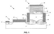
- FIG. 2is a greatly enlarged schematic cross-sectional view of the superlattice as shown in FIG. 1 .
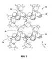
- FIG. 3is a perspective schematic atomic diagram of a portion of the superlattice shown in FIG. 2 .
- FIG. 4is a greatly enlarged schematic cross-sectional view of another embodiment of a superlattice that may be used in the device of FIG. 1 .
- FIG. 5Ais a graph of the calculated band structure from the gamma point (G) for both bulk silicon as in the prior art, and for the 4/1 Si/O superlattice as shown in FIGS. 2 .
- FIG. 5Bis a graph of the calculated band structure from the Z point for both bulk silicon as in the prior art, and for the 4/1 Si/O superlattice as shown in FIG. 2 .
- FIG. 5Cis a graph of the calculated band structure from both the gamma and Z points for both bulk silicon as in the prior art, and for the 5/1/3/1 Si/O superlattice as shown in FIG. 4 .
- the present inventionrelates to controlling the properties of semiconductor materials at the atomic or molecular level to achieve improved performance within semiconductor devices. Further, the invention relates to the identification, creation, and use of improved materials for use in the conduction paths of semiconductor devices.
- fis the Fermi-Dirac distribution
- E Fis the Fermi energy
- Tis the temperature (Kelvin)
- E(k,n)is the energy of an electron in the state corresponding to wave vector k and the n th energy band
- the indices i and jrefer to Cartesian coordinates x, y and z
- the integralsare taken over the Brillouin zone (B.Z.)
- the summationsare taken over bands with energies above and below the Fermi energy for electrons and holes respectively.
- the conductivity reciprocal effective mass tensoris such that a tensorial component of the conductivity of the material is greater for greater values of the corresponding component of the conductivity reciprocal effective mass tensor.
- the superlattices described hereinset the values of the conductivity reciprocal effective mass tensor so as to enhance the conductive properties of the material, such as typically for a preferred direction of charge carrier transport.
- the inverse of the appropriate tensor elementis referred to as the conductivity effective mass.
- the conductivity effective mass for electrons/holes as described above and calculated in the direction of intended carrier transportis used to distinguish improved materials.
- One such examplewould be a superlattice 25 material used to improve temperature characteristics in a semiconductor device, such as a negative differential resistance (NDR) device.
- NDRnegative differential resistance
- FIG. 1one such example is a memory cell 20 which illustratively includes an NDR device, namely a thyristor 21 .
- the memory cell 20further includes a control gate 22 that is coupled to and surrounds the thyristor 21 .
- An access transistor 23is also coupled to the thyristor 21 , and shares a diffused region with it.
- the thyristor 21illustratively includes a plurality of vertically stacked semiconductor layers 26 through 29 having alternating first and second conductivity types on a semiconductor substrate 24 .
- the semiconductor layer 26is the bottom layer of the vertical stack and has an N conductivity type (N+), and the substrate 24 has a P conductivity type.
- the next layer up in the stackis the layer 27 which has a P conductivity type, and the next layer thereon is the layer 28 , which has an N conductivity type.
- the layer 29is the uppermost layer of the stack and it has a P conductivity type (P+).
- the order of conductivity types in the layersmay be different (e.g., P—N—P—N rather than N—P—N—P), and the relative dopant concentrations may also be different.
- the layers 26 through 29are described as being “stacked” herein, this does not mean that these layers have to be separately formed or deposited. That is, a “stacked” layer may also be formed simply by doping a semiconductor region to have different conductivity types adjacent one another, as is the case with the formation of the layer 26 in the illustrated example.
- the control gate 22can be metal, doped silicon, silicide, or salicide and also serves as a first word line for the memory cell 20 , as will be appreciated by those skilled in the art.
- the control gate 22is coupled between a pair of layers of the stack of semiconductor layers having the same conductivity type, namely the bottom N+ layer 26 and the N layer 28 in the present example.
- the thyristor 21further illustratively includes a voltage reference contact 35 , which may also be metal, on the uppermost layer 29 of the stack. Other reliable contact materials may also be used.
- the access transistor 23illustratively includes source and drain regions 30 , 31 , which have an N conductivity type (N+). More particularly, the same doping step which forms the N+ layer 26 of the thyristor 21 layer stack also forms the drain regions 31 , as will be appreciated by those skilled in the art.
- a gate 32 of the access transistor 23overlies the substrate 32 and is connected between the source and drain regions 30 , 31 as shown.
- the gate 32can be doped silicon, silicide, or polycide metal in the exemplary embodiment and also provides a second word line for the memory cell 20 .
- the thyristor 21may therefore be conceptually viewed as a vertical device, and the access transistor 23 as a lateral device in the illustrated embodiment. Yet, in other embodiments different layouts or configurations of the thyristor 21 and/or access transistor 23 may be used, as will be appreciated by those skilled in the art.
- the above-described memory cell 20may be made using conventional semiconductor processing and doping techniques, as will be appreciated by those skilled in the art. Further information regarding the structure of the above-described thyristor SRAM cell (T-RAM) is provided in U.S. Pat. No. 6,229,161 to Nemati et al. (the '161 patent), which is hereby incorporated herein by reference in its entirety.
- VFBforward breakover voltage
- the uppermost layer 29 of the stack of semiconductor layers of the thyristor 21advantageously comprises the superlattice 25 .
- the structure of the band-engineered superlattice 25will help prevent VFB from dropping below the reference voltage VREF. This is due to the behavior over temperature of the non-semiconductor energy-band modifying layer(s) present in the superlattice 25 , and in particular, the change is current versus temperature to keep the cell on, as will be discussed further below.
- the superlattice 25may occupy only a portion of the uppermost layer 29 , the entire layer, or it may extend into the N layer 28 as shown in FIG. 1 or completely through the N layer (not shown). In other embodiments the superlattice 25 may instead or in addition be used in other layers or regions of the memory cell 20 .
- the superlattice 25has a structure that is controlled at the atomic or molecular level and may be formed using known techniques of atomic or molecular layer deposition.
- the superlattice 25includes a plurality of layer groups 45 a - 45 n arranged in stacked relation, as noted above, as perhaps best understood with specific reference to the schematic cross-sectional view of FIG. 2 .
- Each group of layers 45 a - 45 n of the superlattice 25illustratively includes a plurality of stacked base semiconductor monolayers 46 defining a respective base semiconductor portion 46 a - 46 n and an energy band-modifying layer 50 thereon.
- the energy band-modifying layers 50are indicated by stippling in FIG. 2 for clarity of illustration.
- the energy-band modifying layer 50illustratively includes one non-semiconductor monolayer constrained within a crystal lattice of adjacent base semiconductor portions. That is, opposing base semiconductor monolayers 46 in adjacent groups of layers 45 a - 45 n are chemically bound together. For example, in the case of silicon monolayers 46 , some of the silicon atoms in the upper or top semiconductor monolayer of the group of monolayers 46 a will be covalently bonded with silicon atoms in the lower or bottom monolayer of the group 46 b. This allows the crystal lattice to continue through the groups of layers despite the presence of the non-semiconductor monolayer(s) (e.g., oxygen monolayer(s)).
- the non-semiconductor monolayer(s)e.g., oxygen monolayer(s)
- more than one non-semiconductor layer monolayermay be possible.
- the number of non-semiconductor monolayers in the energy band-modifying layer 50may preferably be less than about five monolayers to thereby provide desired energy band-modifying properties.
- non-semiconductor or semiconductor monolayermeans that the material used for the monolayer would be a non-semiconductor or semiconductor if formed in bulk. That is, a single monolayer of a material, such as semiconductor, may not necessarily exhibit the same properties that it would if formed in bulk or in a relatively thick layer, as will be appreciated by those skilled in the art.
- energy band-modifying layers 50 and adjacent base semiconductor portions 46 a - 46 ncause the superlattice 25 to have a lower appropriate conductivity effective mass for the charge carriers in the parallel layer direction than would otherwise be present.
- this parallel directionis orthogonal to the stacking direction.
- the band modifying layers 50may also cause the superlattice 25 to have a common energy band structure, while also advantageously functioning as an insulator between layers or regions vertically above and below the superlattice.
- this structurealso advantageously provides a barrier to dopant and/or material bleed or diffusion and to carrier flow between layers vertically above and below the superlattice 25 .
- the superlattice 25provides a higher charge carrier mobility based upon the lower conductivity effective mass than would otherwise be present.
- all of the above-described properties of the superlattice 25need not be utilized in every application.
- the superlattice 25may only be used for its dopant blocking/insulation properties or its enhanced mobility, or it may be used for both in other applications, as will be appreciated by those skilled in the art.
- a cap layer 52is on an upper layer group 45 n of the superlattice 25 .
- the cap layer 52may comprise a plurality of base semiconductor monolayers 46 .
- the cap layer 52may have between 2 to 100 monolayers of the base semiconductor, and, more preferably between 10 to 50 monolayers. Other thicknesses may be used as well.
- Each base semiconductor portion 46 a - 46 nmay comprise a base semiconductor selected from the group consisting of Group IV semiconductors, Group III-V semiconductors, and Group II-VI semiconductors.
- Group IV semiconductorsalso includes Group IV-IV semiconductors, as will be appreciated by those skilled in the art.
- the base semiconductormay comprise at least one of silicon and germanium, for example.
- Each energy band-modifying layer 50may comprise a non-semiconductor selected from the group consisting of oxygen, nitrogen, fluorine, and carbon-oxygen, for example.
- the non-semiconductoris also desirably thermally stable through deposition of a next layer to thereby facilitate manufacturing,
- the non-semiconductormay be another inorganic or organic element or compound that is compatible with the given semiconductor processing, as will be appreciated by those skilled in the art.
- the term “monolayer”is meant to include a single atomic layer and also a single molecular layer. It is also noted that the energy band-modifying layer 50 provided by a single monolayer is also meant to include a monolayer wherein not all of the possible sites are occupied. For example, with particular reference to the atomic diagram of FIG. 3 , a 4/1 repeating structure is illustrated for silicon as the base semiconductor material, and oxygen as the energy band-modifying material. Only half of the possible sites for oxygen are occupied.
- this one half occupationwould not necessarily be the case as will be appreciated by those skilled in the art. Indeed it can be seen even in this schematic diagram, that individual atoms of oxygen in a given monolayer are not precisely aligned along a flat plane as will also be appreciated by those of skill in the art of atomic deposition.
- a preferred occupation rangeis from about one-eighth to one-half of the possible oxygen sites being full, although other numbers may be used in certain embodiments.
- Silicon and oxygenare currently widely used in conventional semiconductor processing, and, hence, manufacturers will be readily able to use these materials as described herein.
- Atomic or monolayer depositionis also now widely used. Accordingly, semiconductor devices incorporating the superlattice 25 in accordance with the invention may be readily adopted and implemented, as will be appreciated by those skilled in the art.
- the number of silicon monolayersshould desirably be seven or less so that the energy band of the superlattice is common or relatively uniform throughout to achieve the desired advantages.
- the 4/1 repeating structure shown in FIGS. 2 and 3for Si/O has been modeled to indicate an enhanced mobility for electrons and holes in the X direction.
- the calculated conductivity effective mass for electronsis 0.26 and for the 4/1 SiO superlattice in the X direction it is 0.12 resulting in a ratio of 0.46.
- the calculation for holesyields values of 0.36 for bulk silicon and 0.16 for the 4/1 SilO superlattice resulting in a ratio of 0.44.
- While such a directionally preferential featuremay be desired in certain semiconductor devices, other devices may benefit from a more uniform increase in mobility in any direction parallel to the groups of layers. It may also be beneficial to have an increased mobility for both electrons and holes, or just one of these types of charge carriers, as will be appreciated by those skilled in the art. It may also be beneficial to have a decreased carrier mobility in a direction perpendicular to the groups of layers.
- the lower conductivity effective mass for the 4/1 Si/O embodiment of the superlattice 25may be less than two-thirds the conductivity effective mass than would otherwise occur, and this applies for both electrons and holes.
- the superlattice 25 in the embodiment illustrated in FIG. 1further comprises P type conductivity dopant in the uppermost layer 29 , and N type conductivity in the layer 28 . It may be especially appropriate to dope some portion of the superlattice 25 if the superlattice is to provide a portion of a channel, for example. In other embodiments, it may be preferably to have one or more groups of layers 45 of the superlattice 25 substantially undoped depending upon its position within the device.
- FIG. 4another embodiment of a superlattice 25 ′ in accordance with the invention having different properties is now described.
- a repeating pattern of 3/1/5/1is illustrated. More particularly, the lowest base semiconductor portion 46 a ′ has three monolayers, and the second lowest base semiconductor portion 46 b ′ has five monolayers. This pattern repeats throughout the superlattice 25 ′.
- the energy band-modifying layers 50 ′may each include a single monolayer.
- the enhancement of charge carrier mobilityis independent of orientation in the plane of the layers.
- all of the base semiconductor portions 46 a - 46 n of a superlattice 25may be a same number of monolayers thick. In other embodiments, at least some of the base semiconductor portions 46 a - 46 n may be a different number of monolayers thick. In still other embodiments, all of the base semiconductor portions 46 a - 46 n may be a different number of monolayers thick.
- FIGS. 5A-5Cband structures calculated using Density Functional Theory (DFT) are presented. It is well known in the art that DFT underestimates the absolute value of the bandgap. Hence all bands above the gap may be shifted by an appropriate “scissors correction.” However the shape of the band is known to be much more reliable. The vertical energy axes should be interpreted in this light.
- DFTDensity Functional Theory
- FIG. 5Ashows the calculated band structure from the gamma point (G) for both bulk silicon (represented by continuous lines) and for the 4/1 Si/O superlattice 25 as shown in FIG. 2 (represented by dotted lines).
- the directionsrefer to the unit cell of the 4/1 Si/O structure and not to the conventional unit cell of Si, although the (001) direction in the figure does correspond to the (001) direction of the conventional unit cell of Si, and, hence, shows the expected location of the Si conduction band minimum.
- the (100) and (010) directions in the figurecorrespond to the (110) and ( ⁇ 110) directions of the conventional Si unit cell.
- the bands of Si on the figureare folded to represent them on the appropriate reciprocal lattice directions for the 4/1 Si/O structure.
- the conduction band minimum for the 4/1 Si/O structureis located at the gamma point in contrast to bulk silicon (Si), whereas the valence band minimum occurs at the edge of the Brillouin zone in the (001) direction which we refer to as the Z point.
- the greater curvature of the conduction band minimum for the 4/1 Si/O structurecompared to the curvature of the conduction band minimum for Si owing to the band splitting due to the perturbation introduced by the additional oxygen layer.
- FIG. 5Bshows the calculated band structure from the Z point for both bulk silicon (continuous lines) and for the 4/1 Si/O superlattice 25 (dotted lines) of FIG. 5 .
- This figureillustrates the enhanced curvature of the valence band in the (100) direction.
- FIG. 5Cshows the calculated band structure from both the gamma and Z point for both bulk silicon (continuous lines) and for the 5/1/3/1 Si/O structure of the superlattice 25 ′ of FIG. 4 (dotted lines). Due to the symmetry of the 5/1/3/1 Si/O structure, the calculated band structures in the (100) and (010) directions are equivalent. Thus the conductivity effective mass and mobility are expected to be isotropic in the plane parallel to the layers, i.e. perpendicular to the (001) stacking direction. Note that in the 5/1/3/1 Si/O example the conduction band minimum and the valence band maximum are both at or close to the Z point.
- the appropriate comparison and discriminationmay be made via the conductivity reciprocal effective mass tensor calculation. This leads Applicants to further theorize that the 5/1/3/1 superlattice 25 ′ should be substantially direct bandgap. As will be understood by those skilled in the art, the appropriate matrix element for optical transition is another indicator of the distinction between direct and indirect bandgap behavior.
- the superlattice 25may advantageously be used in other NDR device configurations beyond the T-RAM memory cell 20 shown in FIG. 1 .
- one such NDR deviceis shown in FIG. 6 of the '161 patent.
- Another example in which the superlattice 25 may also be incorporatedis set forth in an article entitled “Full Planar 0.562 ⁇ m 2 T-RAM Cell in a 130 nm SOI CMOS Logic Technology for High-Density High-Performance SRAMs” to Nemati et al., IEEE, 2004, which is hereby incorporated in its entirety by reference.
- the superlattice 25may be incorporated in discrete NDR/thyristor devices that are not incorporated in a memory cell.
Landscapes
- Engineering & Computer Science (AREA)
- Chemical & Material Sciences (AREA)
- Nanotechnology (AREA)
- Physics & Mathematics (AREA)
- Mathematical Physics (AREA)
- Theoretical Computer Science (AREA)
- Crystallography & Structural Chemistry (AREA)
- Insulated Gate Type Field-Effect Transistor (AREA)
Abstract
Description
- This application claims the benefit of U.S. Provisional Application No. 60/685,995, filed May 31, 2005, and is a continuation-in-part of U.S. patent application Ser. No. 10/992,422 filed Nov. 18, 2004, which is a continuation of U.S. patent application Ser. No. 10/647,060 tiled Aug. 22, 2003, now U.S. Pat. No. 6,958,486, which is a continuation-in-part of U.S. patent application Ser. Nos. 10/603,696 and 10/603,621 filed on Jun. 26, 2003, the entire disclosures of which are incorporated by reference herein.
- The present invention relates to the field of semiconductors, and, more particularly, to semiconductors having enhanced properties based upon energy band engineering and associated methods.
- Structures and techniques have been proposed to enhance the performance of semiconductor devices, such as by enhancing the mobility of the charge carriers. For example, U.S. Patent Application No. 2003/0057416 to Currie et al. discloses strained material layers of silicon, silicon-germanium, and relaxed silicon and also including impurity-free zones that would otherwise cause performance degradation. The resulting biaxial strain in the upper silicon layer alters the carrier mobilities enabling higher speed and/or lower power devices. Published U.S. Patent Application No. 2003/0034529 to Fitzgerald et al. discloses a CMOS inverter also based upon similar strained silicon technology.
- U.S. Pat. No. 6,472,685 B2 to Takagi discloses a semiconductor device including a silicon and carbon layer sandwiched between silicon layers so that the conduction band and valence band of the second silicon layer receive a tensile strain. Electrons having a smaller effective mass, and which have been induced by an electric field applied to the gate electrode, are confined in the second silicon layer, thus, an n-channel MOSFET is asserted to have a higher mobility.
- U.S. Pat. No. 4,937,204 to Ishibashi et al. discloses a superlattice in which a plurality of layers, less than eight monolayers, and containing a fractional or binary or a binary compound semiconductor layer, are alternately and epitaxially grown. The direction of main current flow is perpendicular to the layers of the superlattice.
- U.S. Pat. No. 5,357,119 to Wang et al. discloses a Si—Ge short period superlattice with higher mobility achieved by reducing alloy scattering in the superlattice. Along these lines, U.S. Pat. No. 5,683,934 to Candelaria discloses an enhanced mobility MOSFET including a channel layer comprising an alloy of silicon and a second material substitutionally present in the silicon lattice at a percentage that places the channel layer under tensile stress.
- U.S. Pat. No. 5,216,262 to Tsu discloses a quantum well structure comprising two barrier regions and a thin epitaxially grown semiconductor layer sandwiched between the barriers. Each barrier region consists of alternate layers of SiO2/Si with a thickness generally in a range of two to six monolayers. A much thicker section of silicon is sandwiched between the barriers.
- An article entitled “Phenomena in silicon nanostructure devices” also to Tsu and published online Sep. 6, 2000 by Applied Physics and Materials Science & Processing, pp. 391-402 discloses a semiconductor-atomic superlattice (SAS) of silicon and oxygen. The Si/O superlattice is disclosed as useful in a silicon quantum and light-emitting devices. In particular, a green electromuminescence diode structure was constructed and tested. Current flow in the diode structure is vertical, that is, perpendicular to the layers of the SAS. The disclosed SAS may include semiconductor layers separated by adsorbed species such as oxygen atoms, and CO molecules. The silicon growth beyond the adsorbed monolayer of oxygen is described as epitaxial with a fairly low defect density. One SAS structure included a 1.1 nm thick silicon portion that is about eight atomic layers of silicon, and another structure had twice this thickness of silicon. An article to Luo et al. entitled “Chemical Design of Direct-Gap Light-Emitting Silicon” published in Physical Review Letters, Vol. 89, No. 7 (Aug. 12, 2002) further discusses the light emitting SAS structures of Tsu.
- Published International Application WO 02/103,767 A1 to Wang, Tsu and Lofgren, discloses a barrier building block of thin silicon and oxygen, carbon, nitrogen, phosphorous, antimony, arsenic or hydrogen to thereby reduce current flowing vertically through the lattice more than four orders of magnitude. The insulating layer/barrier layer allows for low defect epitaxial silicon to be deposited next to the insulating layer.
- Published Great Britain Patent Application 2,347,520 to Mears et al. discloses that principles of Aperiodic Photonic Band-Gap (APBG) structures may be adapted for electronic bandgap engineering. In particular, the application discloses that material parameters, for example, the location of band minima, effective mass, etc, can be tailored to yield new aperiodic materials with desirable band-structure characteristics. Other parameters, such as electrical conductivity, thermal conductivity and dielectric permittivity or magnetic permeability are disclosed as also possible to be designed into the material.
- The present invention relates to the field of semiconductors, and, more particularly, to semiconductors having enhanced properties such as may be based upon energy band engineering and associated methods.
- This and other objects, features, and advantages are provided by a semiconductor device including at least one memory cell comprising a negative differential resistance (NDR) device and a control gate coupled thereto. The NDR device may include a superlattice including a plurality of stacked groups of layers, with each group of layers of the superlattice including a plurality of stacked base semiconductor monolayers defining a base semiconductor portion and at least one non-semiconductor monolayer constrained within a crystal lattice of adjacent base semiconductor portions.
- By way of example, the NDR device may be a thyristor. More particularly, the thyristor may include a plurality of stacked semiconductor layers having alternating first and second conductivity types. Moreover, an uppermost layer of the stack of semiconductor layers may include the superlattice. Furthermore, at least one other layer of the plurality of stacked semiconductor layers beneath the uppermost layer may also include the superlattice, and the thyristor may further include a voltage reference contact on the uppermost layer of the plurality of stacked semiconductor layers. In addition, the control gate may be coupled between a pair of adjacent first and second conductivity type layers in the stack of semiconductor layers. The at least one memory cell may further include at least one access transistor coupled to the NDR device, and the at least one memory cell may include a plurality thereof.
- With respect to the superlattice, the base semiconductor may include silicon, and the at least one non-semiconductor monolayer may include oxygen, for example. More particularly, the at least one non-semiconductor monolayer may include a non-semiconductor selected from the group consisting essentially of oxygen, nitrogen, fluorine, and carbon-oxygen. Further, at least one non-semiconductor monolayer may be a single monolayer thick. All of the base semiconductor portions may be a same number of monolayers thick, or at least some of the base semiconductor portions may be a different number of monolayers thick. Additionally, opposing base semiconductor portions in adjacent groups of layers of the at least one superlattice may be chemically bound together.
FIG. 1 is a cross-sectional view of a semiconductor device in accordance with the present invention including a superlattice.FIG. 2 is a greatly enlarged schematic cross-sectional view of the superlattice as shown inFIG. 1 .FIG. 3 is a perspective schematic atomic diagram of a portion of the superlattice shown inFIG. 2 .FIG. 4 is a greatly enlarged schematic cross-sectional view of another embodiment of a superlattice that may be used in the device ofFIG. 1 .FIG. 5A is a graph of the calculated band structure from the gamma point (G) for both bulk silicon as in the prior art, and for the 4/1 Si/O superlattice as shown inFIGS. 2 .FIG. 5B is a graph of the calculated band structure from the Z point for both bulk silicon as in the prior art, and for the 4/1 Si/O superlattice as shown inFIG. 2 .FIG. 5C is a graph of the calculated band structure from both the gamma and Z points for both bulk silicon as in the prior art, and for the 5/1/3/1 Si/O superlattice as shown inFIG. 4 .- The present invention will now be described more fully hereinafter with reference to the accompanying drawings, in which preferred embodiments of the invention are shown. This invention may, however, be embodied in many different forms and should not be construed as limited to the embodiments set forth herein. Rather, these embodiments are provided so that this disclosure will be thorough and complete, and will fully convey the scope of the invention to those skilled in the art. Like numbers refer to like elements throughout, and prime notation is used to indicate similar elements in alternate embodiments.
- The present invention relates to controlling the properties of semiconductor materials at the atomic or molecular level to achieve improved performance within semiconductor devices. Further, the invention relates to the identification, creation, and use of improved materials for use in the conduction paths of semiconductor devices.
- Applicants theorize, without wishing to be bound thereto, that certain superlattices as described herein reduce the effective mass of charge carriers and that this thereby leads to higher charge carrier mobility. Effective mass is described with various definitions in the literature. As a measure of the improvement in effective mass Applicants use a “conductivity reciprocal effective mass tensor”, Me−1and Mh−1for electrons and holes respectively, defined as:
for electrons and:
for holes, where f is the Fermi-Dirac distribution, EFis the Fermi energy, T is the temperature (Kelvin), E(k,n) is the energy of an electron in the state corresponding to wave vector k and the nthenergy band, the indices i and j refer to Cartesian coordinates x, y and z, the integrals are taken over the Brillouin zone (B.Z.), and the summations are taken over bands with energies above and below the Fermi energy for electrons and holes respectively. - Applicants' definition of the conductivity reciprocal effective mass tensor is such that a tensorial component of the conductivity of the material is greater for greater values of the corresponding component of the conductivity reciprocal effective mass tensor. Again Applicants theorize without wishing to be bound thereto that the superlattices described herein set the values of the conductivity reciprocal effective mass tensor so as to enhance the conductive properties of the material, such as typically for a preferred direction of charge carrier transport. The inverse of the appropriate tensor element is referred to as the conductivity effective mass. In other words, to characterize semiconductor material structures, the conductivity effective mass for electrons/holes as described above and calculated in the direction of intended carrier transport is used to distinguish improved materials.
- Using the abovedescribed measures, one can select materials having improved band structures for specific purposes. One such example would be a
superlattice 25 material used to improve temperature characteristics in a semiconductor device, such as a negative differential resistance (NDR) device. Referring more particularly toFIG. 1 , one such example is amemory cell 20 which illustratively includes an NDR device, namely athyristor 21. Thememory cell 20 further includes acontrol gate 22 that is coupled to and surrounds thethyristor 21. Anaccess transistor 23 is also coupled to thethyristor 21, and shares a diffused region with it. - The
thyristor 21 illustratively includes a plurality of vertically stacked semiconductor layers26 through29 having alternating first and second conductivity types on asemiconductor substrate 24. In the present example, thesemiconductor layer 26 is the bottom layer of the vertical stack and has an N conductivity type (N+), and thesubstrate 24 has a P conductivity type. The next layer up in the stack is thelayer 27 which has a P conductivity type, and the next layer thereon is thelayer 28, which has an N conductivity type. Thelayer 29 is the uppermost layer of the stack and it has a P conductivity type (P+). - It will be appreciated by those skilled in the art that in other embodiments the order of conductivity types in the layers may be different (e.g., P—N—P—N rather than N—P—N—P), and the relative dopant concentrations may also be different. It should also be noted that although the
layers 26 through29 are described as being “stacked” herein, this does not mean that these layers have to be separately formed or deposited. That is, a “stacked” layer may also be formed simply by doping a semiconductor region to have different conductivity types adjacent one another, as is the case with the formation of thelayer 26 in the illustrated example. - The
control gate 22 can be metal, doped silicon, silicide, or salicide and also serves as a first word line for thememory cell 20, as will be appreciated by those skilled in the art. Thecontrol gate 22 is coupled between a pair of layers of the stack of semiconductor layers having the same conductivity type, namely thebottom N+ layer 26 and theN layer 28 in the present example. Thethyristor 21 further illustratively includes avoltage reference contact 35, which may also be metal, on theuppermost layer 29 of the stack. Other reliable contact materials may also be used. - The
access transistor 23 illustratively includes source and drainregions N+ layer 26 of thethyristor 21 layer stack also forms thedrain regions 31, as will be appreciated by those skilled in the art. In addition, agate 32 of theaccess transistor 23 overlies thesubstrate 32 and is connected between the source and drainregions gate 32 can be doped silicon, silicide, or polycide metal in the exemplary embodiment and also provides a second word line for thememory cell 20. Thethyristor 21 may therefore be conceptually viewed as a vertical device, and theaccess transistor 23 as a lateral device in the illustrated embodiment. Yet, in other embodiments different layouts or configurations of thethyristor 21 and/oraccess transistor 23 may be used, as will be appreciated by those skilled in the art. - The above-described
memory cell 20 may be made using conventional semiconductor processing and doping techniques, as will be appreciated by those skilled in the art. Further information regarding the structure of the above-described thyristor SRAM cell (T-RAM) is provided in U.S. Pat. No. 6,229,161 to Nemati et al. (the '161 patent), which is hereby incorporated herein by reference in its entirety. - One of the factors that determines the relative performance of a T-PAM cell such as the one disclosed in the '161 patent when compared to other SKAM cells is the amount of current per cell needed to hold the cell in the “on” state. This current is reported to be in the range of 1 pA for a cylindrical cell having a diameter of 0.5 μm. Another device parameter of interest is the forward breakover voltage, VFB. This voltage is related to the forward voltage of the P+-to-N diode in the thyristor, and decreases with temperature. If VFB drops below the reference voltage VREF, the reference voltage on the anode of the thyristor, the T-RAM cell will ordinarily lose its bistable behavior.
- To address this problem, in the T-
RAM cell 20 theuppermost layer 29 of the stack of semiconductor layers of thethyristor 21 advantageously comprises thesuperlattice 25. Applicants theorize, without wishing to be bound thereto, that the structure of the band-engineeredsuperlattice 25 will help prevent VFB from dropping below the reference voltage VREF. This is due to the behavior over temperature of the non-semiconductor energy-band modifying layer(s) present in thesuperlattice 25, and in particular, the change is current versus temperature to keep the cell on, as will be discussed further below. - The
superlattice 25 may occupy only a portion of theuppermost layer 29, the entire layer, or it may extend into theN layer 28 as shown inFIG. 1 or completely through the N layer (not shown). In other embodiments thesuperlattice 25 may instead or in addition be used in other layers or regions of thememory cell 20. Referring now additionally toFIGS. 2 and 3 , thesuperlattice 25 has a structure that is controlled at the atomic or molecular level and may be formed using known techniques of atomic or molecular layer deposition. Thesuperlattice 25 includes a plurality of layer groups45a-45narranged in stacked relation, as noted above, as perhaps best understood with specific reference to the schematic cross-sectional view ofFIG. 2 . - Each group of layers45a-45nof the
superlattice 25 illustratively includes a plurality of stackedbase semiconductor monolayers 46 defining a respectivebase semiconductor portion 46a-46nand an energy band-modifyinglayer 50 thereon. The energy band-modifyinglayers 50 are indicated by stippling inFIG. 2 for clarity of illustration. - The energy-
band modifying layer 50 illustratively includes one non-semiconductor monolayer constrained within a crystal lattice of adjacent base semiconductor portions. That is, opposingbase semiconductor monolayers 46 in adjacent groups of layers45a-45nare chemically bound together. For example, in the case ofsilicon monolayers 46, some of the silicon atoms in the upper or top semiconductor monolayer of the group ofmonolayers 46awill be covalently bonded with silicon atoms in the lower or bottom monolayer of thegroup 46b.This allows the crystal lattice to continue through the groups of layers despite the presence of the non-semiconductor monolayer(s) (e.g., oxygen monolayer(s)). Of course, there will not be a complete or pure covalent bond between the opposing silicon layers46 of adjacent groups45a-45nas some of the silicon atoms in each of these layers will be bonded to non-semiconductor atoms (i.e., oxygen in the present example), as will be appreciated by those skilled in the art. - In other embodiments, more than one non-semiconductor layer monolayer may be possible. By way of example, the number of non-semiconductor monolayers in the energy band-modifying
layer 50 may preferably be less than about five monolayers to thereby provide desired energy band-modifying properties. - It should be noted that reference herein to a non-semiconductor or semiconductor monolayer means that the material used for the monolayer would be a non-semiconductor or semiconductor if formed in bulk. That is, a single monolayer of a material, such as semiconductor, may not necessarily exhibit the same properties that it would if formed in bulk or in a relatively thick layer, as will be appreciated by those skilled in the art.
- Applicants theorize without wishing to be bound thereto that energy band-modifying
layers 50 and adjacentbase semiconductor portions 46a-46ncause thesuperlattice 25 to have a lower appropriate conductivity effective mass for the charge carriers in the parallel layer direction than would otherwise be present. Considered another way, this parallel direction is orthogonal to the stacking direction. Theband modifying layers 50 may also cause thesuperlattice 25 to have a common energy band structure, while also advantageously functioning as an insulator between layers or regions vertically above and below the superlattice. Moreover, as noted above, this structure also advantageously provides a barrier to dopant and/or material bleed or diffusion and to carrier flow between layers vertically above and below thesuperlattice 25. - It is also theorized that the
superlattice 25 provides a higher charge carrier mobility based upon the lower conductivity effective mass than would otherwise be present. Of course, all of the above-described properties of thesuperlattice 25 need not be utilized in every application. For example, in some applications thesuperlattice 25 may only be used for its dopant blocking/insulation properties or its enhanced mobility, or it may be used for both in other applications, as will be appreciated by those skilled in the art. - A
cap layer 52 is on anupper layer group 45nof thesuperlattice 25. Thecap layer 52 may comprise a plurality ofbase semiconductor monolayers 46. Thecap layer 52 may have between 2 to 100 monolayers of the base semiconductor, and, more preferably between 10 to 50 monolayers. Other thicknesses may be used as well. - Each
base semiconductor portion 46a-46nmay comprise a base semiconductor selected from the group consisting of Group IV semiconductors, Group III-V semiconductors, and Group II-VI semiconductors. Of course, the term Group IV semiconductors also includes Group IV-IV semiconductors, as will be appreciated by those skilled in the art. More particularly, the base semiconductor may comprise at least one of silicon and germanium, for example. - Each energy band-modifying
layer 50 may comprise a non-semiconductor selected from the group consisting of oxygen, nitrogen, fluorine, and carbon-oxygen, for example. The non-semiconductor is also desirably thermally stable through deposition of a next layer to thereby facilitate manufacturing, In other embodiments, the non-semiconductor may be another inorganic or organic element or compound that is compatible with the given semiconductor processing, as will be appreciated by those skilled in the art. - It should be noted that the term “monolayer” is meant to include a single atomic layer and also a single molecular layer. It is also noted that the energy band-modifying
layer 50 provided by a single monolayer is also meant to include a monolayer wherein not all of the possible sites are occupied. For example, with particular reference to the atomic diagram ofFIG. 3 , a 4/1 repeating structure is illustrated for silicon as the base semiconductor material, and oxygen as the energy band-modifying material. Only half of the possible sites for oxygen are occupied. - In other embodiments and/or with different materials this one half occupation would not necessarily be the case as will be appreciated by those skilled in the art. Indeed it can be seen even in this schematic diagram, that individual atoms of oxygen in a given monolayer are not precisely aligned along a flat plane as will also be appreciated by those of skill in the art of atomic deposition. By way of example, a preferred occupation range is from about one-eighth to one-half of the possible oxygen sites being full, although other numbers may be used in certain embodiments.
- Silicon and oxygen are currently widely used in conventional semiconductor processing, and, hence, manufacturers will be readily able to use these materials as described herein. Atomic or monolayer deposition is also now widely used. Accordingly, semiconductor devices incorporating the
superlattice 25 in accordance with the invention may be readily adopted and implemented, as will be appreciated by those skilled in the art. - It is theorized without wishing to be bound thereto, that for a superlattice, such as the Si/O superlattice, for example, that the number of silicon monolayers should desirably be seven or less so that the energy band of the superlattice is common or relatively uniform throughout to achieve the desired advantages. The 4/1 repeating structure shown in
FIGS. 2 and 3 , for Si/O has been modeled to indicate an enhanced mobility for electrons and holes in the X direction. For example, the calculated conductivity effective mass for electrons (isotropic for bulk silicon) is 0.26 and for the 4/1 SiO superlattice in the X direction it is 0.12 resulting in a ratio of 0.46. Similarly, the calculation for holes yields values of 0.36 for bulk silicon and 0.16 for the 4/1 SilO superlattice resulting in a ratio of 0.44. - While such a directionally preferential feature may be desired in certain semiconductor devices, other devices may benefit from a more uniform increase in mobility in any direction parallel to the groups of layers. It may also be beneficial to have an increased mobility for both electrons and holes, or just one of these types of charge carriers, as will be appreciated by those skilled in the art. It may also be beneficial to have a decreased carrier mobility in a direction perpendicular to the groups of layers.
- The lower conductivity effective mass for the 4/1 Si/O embodiment of the
superlattice 25 may be less than two-thirds the conductivity effective mass than would otherwise occur, and this applies for both electrons and holes. Of course, thesuperlattice 25 in the embodiment illustrated inFIG. 1 further comprises P type conductivity dopant in theuppermost layer 29, and N type conductivity in thelayer 28. It may be especially appropriate to dope some portion of thesuperlattice 25 if the superlattice is to provide a portion of a channel, for example. In other embodiments, it may be preferably to have one or more groups of layers45 of thesuperlattice 25 substantially undoped depending upon its position within the device. - Referring now additionally to
FIG. 4 , another embodiment of asuperlattice 25′ in accordance with the invention having different properties is now described. In this embodiment, a repeating pattern of 3/1/5/1 is illustrated. More particularly, the lowestbase semiconductor portion 46a′ has three monolayers, and the second lowestbase semiconductor portion 46b′ has five monolayers. This pattern repeats throughout thesuperlattice 25′. The energy band-modifyinglayers 50′ may each include a single monolayer. For such asuperlattice 25′ including Si/O, the enhancement of charge carrier mobility is independent of orientation in the plane of the layers. Those other elements ofFIG. 4 not specifically mentioned are similar to those discussed above with reference toFIG. 2 and need no further discussion herein. - In some device embodiments, all of the
base semiconductor portions 46a-46nof asuperlattice 25 may be a same number of monolayers thick. In other embodiments, at least some of thebase semiconductor portions 46a-46nmay be a different number of monolayers thick. In still other embodiments, all of thebase semiconductor portions 46a-46nmay be a different number of monolayers thick. - In
FIGS. 5A-5C band structures calculated using Density Functional Theory (DFT) are presented. It is well known in the art that DFT underestimates the absolute value of the bandgap. Hence all bands above the gap may be shifted by an appropriate “scissors correction.” However the shape of the band is known to be much more reliable. The vertical energy axes should be interpreted in this light. FIG. 5A shows the calculated band structure from the gamma point (G) for both bulk silicon (represented by continuous lines) and for the 4/1 Si/O superlattice 25 as shown inFIG. 2 (represented by dotted lines). The directions refer to the unit cell of the 4/1 Si/O structure and not to the conventional unit cell of Si, although the (001) direction in the figure does correspond to the (001) direction of the conventional unit cell of Si, and, hence, shows the expected location of the Si conduction band minimum. The (100) and (010) directions in the figure correspond to the (110) and (−110) directions of the conventional Si unit cell. Those skilled in the art will appreciate that the bands of Si on the figure are folded to represent them on the appropriate reciprocal lattice directions for the 4/1 Si/O structure.- It can be seen that the conduction band minimum for the 4/1 Si/O structure is located at the gamma point in contrast to bulk silicon (Si), whereas the valence band minimum occurs at the edge of the Brillouin zone in the (001) direction which we refer to as the Z point. One may also note the greater curvature of the conduction band minimum for the 4/1 Si/O structure compared to the curvature of the conduction band minimum for Si owing to the band splitting due to the perturbation introduced by the additional oxygen layer.
FIG. 5B shows the calculated band structure from the Z point for both bulk silicon (continuous lines) and for the 4/1 Si/O superlattice25 (dotted lines) ofFIG. 5 . This figure illustrates the enhanced curvature of the valence band in the (100) direction.FIG. 5C shows the calculated band structure from both the gamma and Z point for both bulk silicon (continuous lines) and for the 5/1/3/1 Si/O structure of thesuperlattice 25′ ofFIG. 4 (dotted lines). Due to the symmetry of the 5/1/3/1 Si/O structure, the calculated band structures in the (100) and (010) directions are equivalent. Thus the conductivity effective mass and mobility are expected to be isotropic in the plane parallel to the layers, i.e. perpendicular to the (001) stacking direction. Note that in the 5/1/3/1 Si/O example the conduction band minimum and the valence band maximum are both at or close to the Z point.- Although increased curvature is an indication of reduced effective mass, the appropriate comparison and discrimination may be made via the conductivity reciprocal effective mass tensor calculation. This leads Applicants to further theorize that the 5/1/3/1
superlattice 25′ should be substantially direct bandgap. As will be understood by those skilled in the art, the appropriate matrix element for optical transition is another indicator of the distinction between direct and indirect bandgap behavior. - It should be noted that the
superlattice 25 may advantageously be used in other NDR device configurations beyond the T-RAM memory cell 20 shown inFIG. 1 . By way of example, one such NDR device is shown inFIG. 6 of the '161 patent. Another example in which thesuperlattice 25 may also be incorporated is set forth in an article entitled “Full Planar 0.562 μm2T-RAM Cell in a 130 nm SOI CMOS Logic Technology for High-Density High-Performance SRAMs” to Nemati et al., IEEE, 2004, which is hereby incorporated in its entirety by reference. Moreover, it should also be noted that thesuperlattice 25 may be incorporated in discrete NDR/thyristor devices that are not incorporated in a memory cell. - Many modifications and other embodiments will come to the mind of one skilled in the art having the benefit of the teachings presented in the foregoing descriptions and the associated drawings. Therefore, it is understood that such modifications and embodiments are intended to be included within the scope of the appended claims.
Claims (24)
Priority Applications (1)
| Application Number | Priority Date | Filing Date | Title |
|---|---|---|---|
| US11/420,876US7531850B2 (en) | 2003-06-26 | 2006-05-30 | Semiconductor device including a memory cell with a negative differential resistance (NDR) device |
Applications Claiming Priority (6)
| Application Number | Priority Date | Filing Date | Title |
|---|---|---|---|
| US10/603,696US20040262594A1 (en) | 2003-06-26 | 2003-06-26 | Semiconductor structures having improved conductivity effective mass and methods for fabricating same |
| US10/603,621US20040266116A1 (en) | 2003-06-26 | 2003-06-26 | Methods of fabricating semiconductor structures having improved conductivity effective mass |
| US10/647,060US6958486B2 (en) | 2003-06-26 | 2003-08-22 | Semiconductor device including band-engineered superlattice |
| US10/992,422US7071119B2 (en) | 2003-06-26 | 2004-11-18 | Method for making a semiconductor device including band-engineered superlattice having 3/1-5/1 germanium layer structure |
| US68599505P | 2005-05-31 | 2005-05-31 | |
| US11/420,876US7531850B2 (en) | 2003-06-26 | 2006-05-30 | Semiconductor device including a memory cell with a negative differential resistance (NDR) device |
Related Parent Applications (1)
| Application Number | Title | Priority Date | Filing Date |
|---|---|---|---|
| US10/992,422Continuation-In-PartUS7071119B2 (en) | 2003-06-26 | 2004-11-18 | Method for making a semiconductor device including band-engineered superlattice having 3/1-5/1 germanium layer structure |
Publications (2)
| Publication Number | Publication Date |
|---|---|
| US20060202189A1true US20060202189A1 (en) | 2006-09-14 |
| US7531850B2 US7531850B2 (en) | 2009-05-12 |
Family
ID=36969884
Family Applications (1)
| Application Number | Title | Priority Date | Filing Date |
|---|---|---|---|
| US11/420,876Expired - LifetimeUS7531850B2 (en) | 2003-06-26 | 2006-05-30 | Semiconductor device including a memory cell with a negative differential resistance (NDR) device |
Country Status (1)
| Country | Link |
|---|---|
| US (1) | US7531850B2 (en) |
Cited By (1)
| Publication number | Priority date | Publication date | Assignee | Title |
|---|---|---|---|---|
| RU2611094C1 (en)* | 2015-10-02 | 2017-02-21 | федеральное государственное автономное образовательное учреждение высшего образования "Национальный исследовательский университет "Высшая школа экономики" | Bistable memory cell based on single-layered nanostructure |
Families Citing this family (72)
| Publication number | Priority date | Publication date | Assignee | Title |
|---|---|---|---|---|
| US20110068915A1 (en)* | 2009-09-23 | 2011-03-24 | ThinAir Wireless, Inc. | Geocoded alert system |
| US9082972B2 (en) | 2012-07-24 | 2015-07-14 | Hewlett-Packard Development Company, L.P. | Bipolar resistive switch heat mitigation |
| CN105900241B (en) | 2013-11-22 | 2020-07-24 | 阿托梅拉公司 | Semiconductor device including superlattice depletion layer stack and related methods |
| WO2015077595A1 (en) | 2013-11-22 | 2015-05-28 | Mears Technologies, Inc. | Vertical semiconductor devices including superlattice punch through stop layer and related methods |
| US9716224B2 (en) | 2014-03-07 | 2017-07-25 | Hewlett Packard Enterprise Development Lp | Memristor devices with a thermally-insulating cladding |
| WO2015191561A1 (en) | 2014-06-09 | 2015-12-17 | Mears Technologies, Inc. | Semiconductor devices with enhanced deterministic doping and related methods |
| US9722046B2 (en) | 2014-11-25 | 2017-08-01 | Atomera Incorporated | Semiconductor device including a superlattice and replacement metal gate structure and related methods |
| US9941359B2 (en) | 2015-05-15 | 2018-04-10 | Atomera Incorporated | Semiconductor devices with superlattice and punch-through stop (PTS) layers at different depths and related methods |
| US9721790B2 (en) | 2015-06-02 | 2017-08-01 | Atomera Incorporated | Method for making enhanced semiconductor structures in single wafer processing chamber with desired uniformity control |
| US9558939B1 (en) | 2016-01-15 | 2017-01-31 | Atomera Incorporated | Methods for making a semiconductor device including atomic layer structures using N2O as an oxygen source |
| US10109342B2 (en) | 2016-05-11 | 2018-10-23 | Atomera Incorporated | Dram architecture to reduce row activation circuitry power and peripheral leakage and related methods |
| US10170603B2 (en) | 2016-08-08 | 2019-01-01 | Atomera Incorporated | Semiconductor device including a resonant tunneling diode structure with electron mean free path control layers |
| US10107854B2 (en) | 2016-08-17 | 2018-10-23 | Atomera Incorporated | Semiconductor device including threshold voltage measurement circuitry |
| US10381242B2 (en) | 2017-05-16 | 2019-08-13 | Atomera Incorporated | Method for making a semiconductor device including a superlattice as a gettering layer |
| US10367064B2 (en) | 2017-06-13 | 2019-07-30 | Atomera Incorporated | Semiconductor device with recessed channel array transistor (RCAT) including a superlattice |
| US10109479B1 (en) | 2017-07-31 | 2018-10-23 | Atomera Incorporated | Method of making a semiconductor device with a buried insulating layer formed by annealing a superlattice |
| WO2019036572A1 (en) | 2017-08-18 | 2019-02-21 | Atomera Incorporated | Semiconductor device and method including non-monocrystalline stringer adjacent a superlattice-sti interface |
| US10355151B2 (en) | 2017-12-15 | 2019-07-16 | Atomera Incorporated | CMOS image sensor including photodiodes with overlying superlattices to reduce crosstalk |
| US10608027B2 (en) | 2017-12-15 | 2020-03-31 | Atomera Incorporated | Method for making CMOS image sensor including stacked semiconductor chips and image processing circuitry including a superlattice |
| US10276625B1 (en) | 2017-12-15 | 2019-04-30 | Atomera Incorporated | CMOS image sensor including superlattice to enhance infrared light absorption |
| US10529757B2 (en) | 2017-12-15 | 2020-01-07 | Atomera Incorporated | CMOS image sensor including pixels with read circuitry having a superlattice |
| US10396223B2 (en) | 2017-12-15 | 2019-08-27 | Atomera Incorporated | Method for making CMOS image sensor with buried superlattice layer to reduce crosstalk |
| US10304881B1 (en) | 2017-12-15 | 2019-05-28 | Atomera Incorporated | CMOS image sensor with buried superlattice layer to reduce crosstalk |
| US10461118B2 (en) | 2017-12-15 | 2019-10-29 | Atomera Incorporated | Method for making CMOS image sensor including photodiodes with overlying superlattices to reduce crosstalk |
| US10608043B2 (en) | 2017-12-15 | 2020-03-31 | Atomera Incorporation | Method for making CMOS image sensor including stacked semiconductor chips and readout circuitry including a superlattice |
| US10615209B2 (en) | 2017-12-15 | 2020-04-07 | Atomera Incorporated | CMOS image sensor including stacked semiconductor chips and readout circuitry including a superlattice |
| US10361243B2 (en) | 2017-12-15 | 2019-07-23 | Atomera Incorporated | Method for making CMOS image sensor including superlattice to enhance infrared light absorption |
| US10367028B2 (en) | 2017-12-15 | 2019-07-30 | Atomera Incorporated | CMOS image sensor including stacked semiconductor chips and image processing circuitry including a superlattice |
| CN111937119B (en) | 2018-03-08 | 2024-07-23 | 阿托梅拉公司 | Semiconductor device including enhanced contact structure with superlattice and related methods |
| US10468245B2 (en) | 2018-03-09 | 2019-11-05 | Atomera Incorporated | Semiconductor device including compound semiconductor materials and an impurity and point defect blocking superlattice |
| US10727049B2 (en) | 2018-03-09 | 2020-07-28 | Atomera Incorporated | Method for making a semiconductor device including compound semiconductor materials and an impurity and point defect blocking superlattice |
| US11355667B2 (en) | 2018-04-12 | 2022-06-07 | Atomera Incorporated | Method for making semiconductor device including vertically integrated optical and electronic devices and comprising a superlattice |
| US11664459B2 (en) | 2018-04-12 | 2023-05-30 | Atomera Incorporated | Method for making an inverted T channel field effect transistor (ITFET) including a superlattice |
| US10566191B1 (en) | 2018-08-30 | 2020-02-18 | Atomera Incorporated | Semiconductor device including superlattice structures with reduced defect densities |
| US10811498B2 (en) | 2018-08-30 | 2020-10-20 | Atomera Incorporated | Method for making superlattice structures with reduced defect densities |
| US10840337B2 (en) | 2018-11-16 | 2020-11-17 | Atomera Incorporated | Method for making a FINFET having reduced contact resistance |
| US10580866B1 (en) | 2018-11-16 | 2020-03-03 | Atomera Incorporated | Semiconductor device including source/drain dopant diffusion blocking superlattices to reduce contact resistance |
| US10580867B1 (en) | 2018-11-16 | 2020-03-03 | Atomera Incorporated | FINFET including source and drain regions with dopant diffusion blocking superlattice layers to reduce contact resistance |
| US10840336B2 (en) | 2018-11-16 | 2020-11-17 | Atomera Incorporated | Semiconductor device with metal-semiconductor contacts including oxygen insertion layer to constrain dopants and related methods |
| US10840335B2 (en) | 2018-11-16 | 2020-11-17 | Atomera Incorporated | Method for making semiconductor device including body contact dopant diffusion blocking superlattice to reduce contact resistance |
| US10847618B2 (en) | 2018-11-16 | 2020-11-24 | Atomera Incorporated | Semiconductor device including body contact dopant diffusion blocking superlattice having reduced contact resistance |
| US10593761B1 (en) | 2018-11-16 | 2020-03-17 | Atomera Incorporated | Method for making a semiconductor device having reduced contact resistance |
| US10854717B2 (en) | 2018-11-16 | 2020-12-01 | Atomera Incorporated | Method for making a FINFET including source and drain dopant diffusion blocking superlattices to reduce contact resistance |
| US11094818B2 (en) | 2019-04-23 | 2021-08-17 | Atomera Incorporated | Method for making a semiconductor device including a superlattice and an asymmetric channel and related methods |
| US10825901B1 (en) | 2019-07-17 | 2020-11-03 | Atomera Incorporated | Semiconductor devices including hyper-abrupt junction region including a superlattice |
| US10868120B1 (en) | 2019-07-17 | 2020-12-15 | Atomera Incorporated | Method for making a varactor with hyper-abrupt junction region including a superlattice |
| US10937868B2 (en) | 2019-07-17 | 2021-03-02 | Atomera Incorporated | Method for making semiconductor devices with hyper-abrupt junction region including spaced-apart superlattices |
| US10937888B2 (en) | 2019-07-17 | 2021-03-02 | Atomera Incorporated | Method for making a varactor with a hyper-abrupt junction region including spaced-apart superlattices |
| US11183565B2 (en) | 2019-07-17 | 2021-11-23 | Atomera Incorporated | Semiconductor devices including hyper-abrupt junction region including spaced-apart superlattices and related methods |
| US10840388B1 (en) | 2019-07-17 | 2020-11-17 | Atomera Incorporated | Varactor with hyper-abrupt junction region including a superlattice |
| US10879357B1 (en) | 2019-07-17 | 2020-12-29 | Atomera Incorporated | Method for making a semiconductor device having a hyper-abrupt junction region including a superlattice |
| US10825902B1 (en) | 2019-07-17 | 2020-11-03 | Atomera Incorporated | Varactor with hyper-abrupt junction region including spaced-apart superlattices |
| US11437487B2 (en) | 2020-01-14 | 2022-09-06 | Atomera Incorporated | Bipolar junction transistors including emitter-base and base-collector superlattices |
| US11177351B2 (en) | 2020-02-26 | 2021-11-16 | Atomera Incorporated | Semiconductor device including a superlattice with different non-semiconductor material monolayers |
| US11302823B2 (en) | 2020-02-26 | 2022-04-12 | Atomera Incorporated | Method for making semiconductor device including a superlattice with different non-semiconductor material monolayers |
| US11075078B1 (en) | 2020-03-06 | 2021-07-27 | Atomera Incorporated | Method for making a semiconductor device including a superlattice within a recessed etch |
| US11569368B2 (en) | 2020-06-11 | 2023-01-31 | Atomera Incorporated | Method for making semiconductor device including a superlattice and providing reduced gate leakage |
| US11469302B2 (en) | 2020-06-11 | 2022-10-11 | Atomera Incorporated | Semiconductor device including a superlattice and providing reduced gate leakage |
| US11837634B2 (en) | 2020-07-02 | 2023-12-05 | Atomera Incorporated | Semiconductor device including superlattice with oxygen and carbon monolayers |
| TWI803219B (en) | 2021-03-03 | 2023-05-21 | 美商安托梅拉公司 | Radio frequency (rf) semiconductor devices including a ground plane layer having a superlattice and associated methods |
| US11810784B2 (en) | 2021-04-21 | 2023-11-07 | Atomera Incorporated | Method for making semiconductor device including a superlattice and enriched silicon 28 epitaxial layer |
| US11923418B2 (en) | 2021-04-21 | 2024-03-05 | Atomera Incorporated | Semiconductor device including a superlattice and enriched silicon 28 epitaxial layer |
| TWI816399B (en) | 2021-05-18 | 2023-09-21 | 美商安托梅拉公司 | Semiconductor device including a superlattice providing metal work function tuning and associated methods |
| US11682712B2 (en) | 2021-05-26 | 2023-06-20 | Atomera Incorporated | Method for making semiconductor device including superlattice with O18 enriched monolayers |
| US11728385B2 (en) | 2021-05-26 | 2023-08-15 | Atomera Incorporated | Semiconductor device including superlattice with O18 enriched monolayers |
| US11631584B1 (en) | 2021-10-28 | 2023-04-18 | Atomera Incorporated | Method for making semiconductor device with selective etching of superlattice to define etch stop layer |
| US11721546B2 (en) | 2021-10-28 | 2023-08-08 | Atomera Incorporated | Method for making semiconductor device with selective etching of superlattice to accumulate non-semiconductor atoms |
| WO2023215382A1 (en) | 2022-05-04 | 2023-11-09 | Atomera Incorporated | Dram sense amplifier architecture with reduced power consumption and related methods |
| WO2024192097A1 (en) | 2023-03-14 | 2024-09-19 | Atomera Incorporated | Method for making a radio frequency silicon-on-insulator (rfsoi) wafer including a superlattice |
| US20240322025A1 (en) | 2023-03-24 | 2024-09-26 | Atomera Incorporated | Nanostructure transistors with flush source/drain dopant blocking structures including a superlattice |
| WO2024233543A1 (en) | 2023-05-08 | 2024-11-14 | Atomera Incorporated | Dmos devices including a superlattice and field plate for drift region diffusion and related methods |
| US12308229B2 (en) | 2023-07-03 | 2025-05-20 | Atomera Incorporated | Method for making memory device including a superlattice gettering layer |
Citations (48)
| Publication number | Priority date | Publication date | Assignee | Title |
|---|---|---|---|---|
| US4485128A (en)* | 1981-11-20 | 1984-11-27 | Chronar Corporation | Bandgap control in amorphous semiconductors |
| US4594603A (en)* | 1982-04-22 | 1986-06-10 | Board Of Trustees Of The University Of Illinois | Semiconductor device with disordered active region |
| US4882609A (en)* | 1984-11-19 | 1989-11-21 | Max-Planck Gesellschaft Zur Forderung Der Wissenschafter E.V. | Semiconductor devices with at least one monoatomic layer of doping atoms |
| US4908678A (en)* | 1986-10-08 | 1990-03-13 | Semiconductor Energy Laboratory Co., Ltd. | FET with a super lattice channel |
| US4937204A (en)* | 1985-03-15 | 1990-06-26 | Sony Corporation | Method of making a superlattice heterojunction bipolar device |
| US4969031A (en)* | 1982-02-03 | 1990-11-06 | Hitachi, Ltd. | Semiconductor devices and method for making the same |
| US5081513A (en)* | 1991-02-28 | 1992-01-14 | Xerox Corporation | Electronic device with recovery layer proximate to active layer |
| US5216262A (en)* | 1992-03-02 | 1993-06-01 | Raphael Tsu | Quantum well structures useful for semiconductor devices |
| US5357119A (en)* | 1993-02-19 | 1994-10-18 | Board Of Regents Of The University Of California | Field effect devices having short period superlattice structures using Si and Ge |
| US5577061A (en)* | 1994-12-16 | 1996-11-19 | Hughes Aircraft Company | Superlattice cladding layers for mid-infrared lasers |
| US5594567A (en)* | 1992-07-24 | 1997-01-14 | Matsushita Electric Industrial Co., Ltd. | Spatial light modulator with a photoconductor having uneven conductivity in a lateral direction and a method for fabricating the same |
| US5606177A (en)* | 1993-10-29 | 1997-02-25 | Texas Instruments Incorporated | Silicon oxide resonant tunneling diode structure |
| US5616515A (en)* | 1994-08-04 | 1997-04-01 | Texas Instruments Incorporated | Silicon oxide germanium resonant tunneling |
| US5627386A (en)* | 1994-08-11 | 1997-05-06 | The United States Of America As Represented By The Secretary Of The Army | Silicon nanostructure light-emitting diode |
| US5683934A (en)* | 1994-09-26 | 1997-11-04 | Motorola, Inc. | Enhanced mobility MOSFET device and method |
| US5684817A (en)* | 1995-05-12 | 1997-11-04 | Thomson-Csf | Semiconductor laser having a structure of photonic bandgap material |
| US5994164A (en)* | 1997-03-18 | 1999-11-30 | The Penn State Research Foundation | Nanostructure tailoring of material properties using controlled crystallization |
| US6058127A (en)* | 1996-12-13 | 2000-05-02 | Massachusetts Institute Of Technology | Tunable microcavity and method of using nonlinear materials in a photonic crystal |
| US6229161B1 (en)* | 1998-06-05 | 2001-05-08 | Stanford University | Semiconductor capacitively-coupled NDR device and its applications in high-density high-speed memories and in power switches |
| US6255150B1 (en)* | 1997-10-23 | 2001-07-03 | Texas Instruments Incorporated | Use of crystalline SiOx barriers for Si-based resonant tunneling diodes |
| US6274007B1 (en)* | 1999-11-25 | 2001-08-14 | Sceptre Electronics Limited | Methods of formation of a silicon nanostructure, a silicon quantum wire array and devices based thereon |
| US6281532B1 (en)* | 1999-06-28 | 2001-08-28 | Intel Corporation | Technique to obtain increased channel mobilities in NMOS transistors by gate electrode engineering |
| US6281518B1 (en)* | 1997-12-04 | 2001-08-28 | Ricoh Company, Ltd. | Layered III-V semiconductor structures and light emitting devices including the structures |
| US6326311B1 (en)* | 1998-03-30 | 2001-12-04 | Sharp Kabushiki Kaisha | Microstructure producing method capable of controlling growth position of minute particle or thin and semiconductor device employing the microstructure |
| US6344271B1 (en)* | 1998-11-06 | 2002-02-05 | Nanoenergy Corporation | Materials and products using nanostructured non-stoichiometric substances |
| US6350993B1 (en)* | 1999-03-12 | 2002-02-26 | International Business Machines Corporation | High speed composite p-channel Si/SiGe heterostructure for field effect devices |
| US6376337B1 (en)* | 1997-11-10 | 2002-04-23 | Nanodynamics, Inc. | Epitaxial SiOx barrier/insulation layer |
| US20020094003A1 (en)* | 1999-09-29 | 2002-07-18 | Xerox Corporation | Structure and method for index-guided buried heterostructure AlGalnN laser diodes |
| US6436784B1 (en)* | 1995-08-03 | 2002-08-20 | Hitachi Europe Limited | Method of forming semiconductor structure |
| US6472685B2 (en)* | 1997-12-03 | 2002-10-29 | Matsushita Electric Industrial Co., Ltd. | Semiconductor device |
| US6498359B2 (en)* | 2000-05-22 | 2002-12-24 | Max-Planck-Gesellschaft Zur Foerderung Der Wissenschaften E.V. | Field-effect transistor based on embedded cluster structures and process for its production |
| US6501092B1 (en)* | 1999-10-25 | 2002-12-31 | Intel Corporation | Integrated semiconductor superlattice optical modulator |
| US6521519B2 (en)* | 1996-12-10 | 2003-02-18 | Mitsubishi Denki Kabushiki Kaisha | MIS transistor and manufacturing method thereof |
| US20030034529A1 (en)* | 2000-12-04 | 2003-02-20 | Amberwave Systems Corporation | CMOS inverter and integrated circuits utilizing strained silicon surface channel MOSFETs |
| US20030057416A1 (en)* | 2001-09-21 | 2003-03-27 | Amberwave Systems Corporation | Semiconductor structures employing strained material layers with defined impurity gradients and methods for fabricating same |
| US20030089899A1 (en)* | 2000-08-22 | 2003-05-15 | Lieber Charles M. | Nanoscale wires and related devices |
| US6608327B1 (en)* | 1998-02-27 | 2003-08-19 | North Carolina State University | Gallium nitride semiconductor structure including laterally offset patterned layers |
| US20030162335A1 (en)* | 1999-01-14 | 2003-08-28 | Matsushita Electric Industrial Co., Ltd. | Semiconductor device and method for fabricating the same |
| US6638838B1 (en)* | 2000-10-02 | 2003-10-28 | Motorola, Inc. | Semiconductor structure including a partially annealed layer and method of forming the same |
| US6646293B2 (en)* | 2001-07-18 | 2003-11-11 | Motorola, Inc. | Structure for fabricating high electron mobility transistors utilizing the formation of complaint substrates |
| US20030215990A1 (en)* | 2002-03-14 | 2003-11-20 | Eugene Fitzgerald | Methods for fabricating strained layers on semiconductor substrates |
| US6673646B2 (en)* | 2001-02-28 | 2004-01-06 | Motorola, Inc. | Growth of compound semiconductor structures on patterned oxide films and process for fabricating same |
| US6690699B2 (en)* | 2001-03-02 | 2004-02-10 | Lucent Technologies Inc | Quantum cascade laser with relaxation-stabilized injection |
| US6711191B1 (en)* | 1999-03-04 | 2004-03-23 | Nichia Corporation | Nitride semiconductor laser device |
| US20040084781A1 (en)* | 1998-08-31 | 2004-05-06 | Micron Technology, Inc. | Compact system module with built-in thermoelectric cooling |
| US6748002B2 (en)* | 1998-08-10 | 2004-06-08 | D-Led Corporation | Injection laser |
| US6816530B2 (en)* | 2002-09-30 | 2004-11-09 | Lucent Technologies Inc. | Nonlinear semiconductor light sources |
| US20040227165A1 (en)* | 2003-04-21 | 2004-11-18 | Nanodynamics, Inc. | Si/C superlattice useful for semiconductor devices |
Family Cites Families (7)
| Publication number | Priority date | Publication date | Assignee | Title |
|---|---|---|---|---|
| JPS6127681A (en) | 1984-07-17 | 1986-02-07 | Res Dev Corp Of Japan | Field effect transistor with superlattice structure channel part |
| JPS61145820A (en) | 1984-12-20 | 1986-07-03 | Seiko Epson Corp | Semiconductor thin film material |
| JPS61220339A (en) | 1985-03-26 | 1986-09-30 | Nippon Telegr & Teleph Corp <Ntt> | Control of characteristics of semiconductor material |
| JPS62219665A (en) | 1986-03-20 | 1987-09-26 | Fujitsu Ltd | Superlattice thin-film transistor |
| EP0843361A1 (en) | 1996-11-15 | 1998-05-20 | Hitachi Europe Limited | Memory device |
| US6888175B1 (en) | 1998-05-29 | 2005-05-03 | Massachusetts Institute Of Technology | Compound semiconductor structure with lattice and polarity matched heteroepitaxial layers |
| GB9905196D0 (en) | 1999-03-05 | 1999-04-28 | Fujitsu Telecommunications Eur | Aperiodic gratings |
- 2006
- 2006-05-30USUS11/420,876patent/US7531850B2/ennot_activeExpired - Lifetime
Patent Citations (53)
| Publication number | Priority date | Publication date | Assignee | Title |
|---|---|---|---|---|
| US4485128A (en)* | 1981-11-20 | 1984-11-27 | Chronar Corporation | Bandgap control in amorphous semiconductors |
| US4969031A (en)* | 1982-02-03 | 1990-11-06 | Hitachi, Ltd. | Semiconductor devices and method for making the same |
| US4594603A (en)* | 1982-04-22 | 1986-06-10 | Board Of Trustees Of The University Of Illinois | Semiconductor device with disordered active region |
| US4882609A (en)* | 1984-11-19 | 1989-11-21 | Max-Planck Gesellschaft Zur Forderung Der Wissenschafter E.V. | Semiconductor devices with at least one monoatomic layer of doping atoms |
| US4937204A (en)* | 1985-03-15 | 1990-06-26 | Sony Corporation | Method of making a superlattice heterojunction bipolar device |
| US4908678A (en)* | 1986-10-08 | 1990-03-13 | Semiconductor Energy Laboratory Co., Ltd. | FET with a super lattice channel |
| US5055887A (en)* | 1986-10-08 | 1991-10-08 | Semiconductor Energy Laboratory Co., Ltd. | Fet with a super lattice channel |
| US5081513A (en)* | 1991-02-28 | 1992-01-14 | Xerox Corporation | Electronic device with recovery layer proximate to active layer |
| US5216262A (en)* | 1992-03-02 | 1993-06-01 | Raphael Tsu | Quantum well structures useful for semiconductor devices |
| US5594567A (en)* | 1992-07-24 | 1997-01-14 | Matsushita Electric Industrial Co., Ltd. | Spatial light modulator with a photoconductor having uneven conductivity in a lateral direction and a method for fabricating the same |
| US5357119A (en)* | 1993-02-19 | 1994-10-18 | Board Of Regents Of The University Of California | Field effect devices having short period superlattice structures using Si and Ge |
| US5606177A (en)* | 1993-10-29 | 1997-02-25 | Texas Instruments Incorporated | Silicon oxide resonant tunneling diode structure |
| US5616515A (en)* | 1994-08-04 | 1997-04-01 | Texas Instruments Incorporated | Silicon oxide germanium resonant tunneling |
| US5627386A (en)* | 1994-08-11 | 1997-05-06 | The United States Of America As Represented By The Secretary Of The Army | Silicon nanostructure light-emitting diode |
| US5683934A (en)* | 1994-09-26 | 1997-11-04 | Motorola, Inc. | Enhanced mobility MOSFET device and method |
| US5577061A (en)* | 1994-12-16 | 1996-11-19 | Hughes Aircraft Company | Superlattice cladding layers for mid-infrared lasers |
| US5684817A (en)* | 1995-05-12 | 1997-11-04 | Thomson-Csf | Semiconductor laser having a structure of photonic bandgap material |
| US6436784B1 (en)* | 1995-08-03 | 2002-08-20 | Hitachi Europe Limited | Method of forming semiconductor structure |
| US6521519B2 (en)* | 1996-12-10 | 2003-02-18 | Mitsubishi Denki Kabushiki Kaisha | MIS transistor and manufacturing method thereof |
| US6058127A (en)* | 1996-12-13 | 2000-05-02 | Massachusetts Institute Of Technology | Tunable microcavity and method of using nonlinear materials in a photonic crystal |
| US5994164A (en)* | 1997-03-18 | 1999-11-30 | The Penn State Research Foundation | Nanostructure tailoring of material properties using controlled crystallization |
| US6255150B1 (en)* | 1997-10-23 | 2001-07-03 | Texas Instruments Incorporated | Use of crystalline SiOx barriers for Si-based resonant tunneling diodes |
| US6376337B1 (en)* | 1997-11-10 | 2002-04-23 | Nanodynamics, Inc. | Epitaxial SiOx barrier/insulation layer |
| US6472685B2 (en)* | 1997-12-03 | 2002-10-29 | Matsushita Electric Industrial Co., Ltd. | Semiconductor device |
| US6281518B1 (en)* | 1997-12-04 | 2001-08-28 | Ricoh Company, Ltd. | Layered III-V semiconductor structures and light emitting devices including the structures |
| US6608327B1 (en)* | 1998-02-27 | 2003-08-19 | North Carolina State University | Gallium nitride semiconductor structure including laterally offset patterned layers |
| US6326311B1 (en)* | 1998-03-30 | 2001-12-04 | Sharp Kabushiki Kaisha | Microstructure producing method capable of controlling growth position of minute particle or thin and semiconductor device employing the microstructure |
| US20060011940A1 (en)* | 1998-06-05 | 2006-01-19 | Farid Nemati | Thyristor-type memory device |
| US6448586B1 (en)* | 1998-06-05 | 2002-09-10 | The Board Of Trustees Of The Leland Standford Junior University | Semiconductor current-switching device having operational enhancer and method therefor |
| US6229161B1 (en)* | 1998-06-05 | 2001-05-08 | Stanford University | Semiconductor capacitively-coupled NDR device and its applications in high-density high-speed memories and in power switches |
| US6748002B2 (en)* | 1998-08-10 | 2004-06-08 | D-Led Corporation | Injection laser |
| US20040084781A1 (en)* | 1998-08-31 | 2004-05-06 | Micron Technology, Inc. | Compact system module with built-in thermoelectric cooling |
| US6344271B1 (en)* | 1998-11-06 | 2002-02-05 | Nanoenergy Corporation | Materials and products using nanostructured non-stoichiometric substances |
| US20030162335A1 (en)* | 1999-01-14 | 2003-08-28 | Matsushita Electric Industrial Co., Ltd. | Semiconductor device and method for fabricating the same |
| US6711191B1 (en)* | 1999-03-04 | 2004-03-23 | Nichia Corporation | Nitride semiconductor laser device |
| US6350993B1 (en)* | 1999-03-12 | 2002-02-26 | International Business Machines Corporation | High speed composite p-channel Si/SiGe heterostructure for field effect devices |
| US6281532B1 (en)* | 1999-06-28 | 2001-08-28 | Intel Corporation | Technique to obtain increased channel mobilities in NMOS transistors by gate electrode engineering |
| US20020094003A1 (en)* | 1999-09-29 | 2002-07-18 | Xerox Corporation | Structure and method for index-guided buried heterostructure AlGalnN laser diodes |
| US6566679B2 (en)* | 1999-10-25 | 2003-05-20 | Intel Corporation | Integrated semiconductor superlattice optical modulator |
| US6501092B1 (en)* | 1999-10-25 | 2002-12-31 | Intel Corporation | Integrated semiconductor superlattice optical modulator |
| US6621097B2 (en)* | 1999-10-25 | 2003-09-16 | Intel Corporation | Integrated semiconductor superlattice optical modulator |
| US6274007B1 (en)* | 1999-11-25 | 2001-08-14 | Sceptre Electronics Limited | Methods of formation of a silicon nanostructure, a silicon quantum wire array and devices based thereon |
| US6498359B2 (en)* | 2000-05-22 | 2002-12-24 | Max-Planck-Gesellschaft Zur Foerderung Der Wissenschaften E.V. | Field-effect transistor based on embedded cluster structures and process for its production |
| US20030089899A1 (en)* | 2000-08-22 | 2003-05-15 | Lieber Charles M. | Nanoscale wires and related devices |
| US6638838B1 (en)* | 2000-10-02 | 2003-10-28 | Motorola, Inc. | Semiconductor structure including a partially annealed layer and method of forming the same |
| US20030034529A1 (en)* | 2000-12-04 | 2003-02-20 | Amberwave Systems Corporation | CMOS inverter and integrated circuits utilizing strained silicon surface channel MOSFETs |
| US6673646B2 (en)* | 2001-02-28 | 2004-01-06 | Motorola, Inc. | Growth of compound semiconductor structures on patterned oxide films and process for fabricating same |
| US6690699B2 (en)* | 2001-03-02 | 2004-02-10 | Lucent Technologies Inc | Quantum cascade laser with relaxation-stabilized injection |
| US6646293B2 (en)* | 2001-07-18 | 2003-11-11 | Motorola, Inc. | Structure for fabricating high electron mobility transistors utilizing the formation of complaint substrates |
| US20030057416A1 (en)* | 2001-09-21 | 2003-03-27 | Amberwave Systems Corporation | Semiconductor structures employing strained material layers with defined impurity gradients and methods for fabricating same |
| US20030215990A1 (en)* | 2002-03-14 | 2003-11-20 | Eugene Fitzgerald | Methods for fabricating strained layers on semiconductor substrates |
| US6816530B2 (en)* | 2002-09-30 | 2004-11-09 | Lucent Technologies Inc. | Nonlinear semiconductor light sources |
| US20040227165A1 (en)* | 2003-04-21 | 2004-11-18 | Nanodynamics, Inc. | Si/C superlattice useful for semiconductor devices |
Cited By (1)
| Publication number | Priority date | Publication date | Assignee | Title |
|---|---|---|---|---|
| RU2611094C1 (en)* | 2015-10-02 | 2017-02-21 | федеральное государственное автономное образовательное учреждение высшего образования "Национальный исследовательский университет "Высшая школа экономики" | Bistable memory cell based on single-layered nanostructure |
Also Published As
| Publication number | Publication date |
|---|---|
| US7531850B2 (en) | 2009-05-12 |
Similar Documents
| Publication | Publication Date | Title |
|---|---|---|
| US7531850B2 (en) | Semiconductor device including a memory cell with a negative differential resistance (NDR) device | |
| EP3497728B1 (en) | Semiconductor device including a resonant tunneling diode structure with electron mean free path control layers comprising a superlattice and associated methods | |
| US10825901B1 (en) | Semiconductor devices including hyper-abrupt junction region including a superlattice | |
| US10840388B1 (en) | Varactor with hyper-abrupt junction region including a superlattice | |
| US7229902B2 (en) | Method for making a semiconductor device including a superlattice with regions defining a semiconductor junction | |
| US7045813B2 (en) | Semiconductor device including a superlattice with regions defining a semiconductor junction | |
| US7227174B2 (en) | Semiconductor device including a superlattice and adjacent semiconductor layer with doped regions defining a semiconductor junction | |
| US7491587B2 (en) | Method for making a semiconductor device having a semiconductor-on-insulator (SOI) configuration and including a superlattice on a thin semiconductor layer | |
| US7045377B2 (en) | Method for making a semiconductor device including a superlattice and adjacent semiconductor layer with doped regions defining a semiconductor junction | |
| US10825902B1 (en) | Varactor with hyper-abrupt junction region including spaced-apart superlattices | |
| US10868120B1 (en) | Method for making a varactor with hyper-abrupt junction region including a superlattice | |
| US9972685B2 (en) | Vertical semiconductor devices including superlattice punch through stop layer and related methods | |
| US20060231857A1 (en) | Method for making a semiconductor device including a memory cell with a negative differential resistance (ndr) device | |
| US7781827B2 (en) | Semiconductor device with a vertical MOSFET including a superlattice and related methods | |
| US7598515B2 (en) | Semiconductor device including a strained superlattice and overlying stress layer and related methods | |
| US10879357B1 (en) | Method for making a semiconductor device having a hyper-abrupt junction region including a superlattice | |
| US10937888B2 (en) | Method for making a varactor with a hyper-abrupt junction region including spaced-apart superlattices | |
| US12046470B2 (en) | Method for making semiconductor device including a superlattice and enriched silicon 28 epitaxial layer | |
| US11177351B2 (en) | Semiconductor device including a superlattice with different non-semiconductor material monolayers | |
| US20070063186A1 (en) | Method for making a semiconductor device including a front side strained superlattice layer and a back side stress layer | |
| US20070063185A1 (en) | Semiconductor device including a front side strained superlattice layer and a back side stress layer | |
| US12439658B2 (en) | Semiconductor device including a superlattice providing metal work function tuning | |
| US11302823B2 (en) | Method for making semiconductor device including a superlattice with different non-semiconductor material monolayers | |
| US20240170539A1 (en) | Semiconductor device including a superlattice and enriched silicon 28 epitaxial layer | |
| US20060289049A1 (en) | Semiconductor Device Having a Semiconductor-on-Insulator (SOI) Configuration and Including a Superlattice on a Thin Semiconductor Layer |
Legal Events
| Date | Code | Title | Description |
|---|---|---|---|
| AS | Assignment | Owner name:RJ MEARS, LLC, MASSACHUSETTS Free format text:ASSIGNMENT OF ASSIGNORS INTEREST;ASSIGNOR:BLANCHARD, RICHARD A.;REEL/FRAME:017692/0241 Effective date:20060526 | |
| AS | Assignment | Owner name:MEARS TECHNOLOGIES, INC., MASSACHUSETTS Free format text:CHANGE OF NAME;ASSIGNOR:RJ MEARS, LLC;REEL/FRAME:019817/0236 Effective date:20070314 Owner name:MEARS TECHNOLOGIES, INC.,MASSACHUSETTS Free format text:CHANGE OF NAME;ASSIGNOR:RJ MEARS, LLC;REEL/FRAME:019817/0236 Effective date:20070314 | |
| STCF | Information on status: patent grant | Free format text:PATENTED CASE | |
| FPAY | Fee payment | Year of fee payment:4 | |
| AS | Assignment | Owner name:LIQUID VENTURE PARTNERS, LLC, CALIFORNIA Free format text:SECURITY INTEREST;ASSIGNOR:MEARS TECHNOLOGIES, INC.;REEL/FRAME:035216/0473 Effective date:20150317 | |
| FEPP | Fee payment procedure | Free format text:PAT HOLDER CLAIMS SMALL ENTITY STATUS, ENTITY STATUS SET TO SMALL (ORIGINAL EVENT CODE: LTOS); ENTITY STATUS OF PATENT OWNER: LARGE ENTITY | |
| AS | Assignment | Owner name:ATOMERA INCORPORATED, CALIFORNIA Free format text:CHANGE OF NAME;ASSIGNOR:MEARS TECHNOLOGIES, INC.;REEL/FRAME:038400/0349 Effective date:20160112 | |
| FPAY | Fee payment | Year of fee payment:8 | |
| FEPP | Fee payment procedure | Free format text:ENTITY STATUS SET TO UNDISCOUNTED (ORIGINAL EVENT CODE: BIG.); ENTITY STATUS OF PATENT OWNER: LARGE ENTITY | |
| AS | Assignment | Owner name:ATOMERA INCORPORATED, CALIFORNIA Free format text:RELEASE BY SECURED PARTY;ASSIGNOR:CLIFFORD, ROBERT;REEL/FRAME:053681/0942 Effective date:20200901 | |
| FEPP | Fee payment procedure | Free format text:11.5 YR SURCHARGE- LATE PMT W/IN 6 MO, LARGE ENTITY (ORIGINAL EVENT CODE: M1556); ENTITY STATUS OF PATENT OWNER: LARGE ENTITY | |
| MAFP | Maintenance fee payment | Free format text:PAYMENT OF MAINTENANCE FEE, 12TH YEAR, LARGE ENTITY (ORIGINAL EVENT CODE: M1553); ENTITY STATUS OF PATENT OWNER: LARGE ENTITY Year of fee payment:12 |