US20060189036A1 - Methods and systems for adhering microfeature workpieces to support members - Google Patents
Methods and systems for adhering microfeature workpieces to support membersDownload PDFInfo
- Publication number
- US20060189036A1 US20060189036A1US11/407,560US40756006AUS2006189036A1US 20060189036 A1US20060189036 A1US 20060189036A1US 40756006 AUS40756006 AUS 40756006AUS 2006189036 A1US2006189036 A1US 2006189036A1
- Authority
- US
- United States
- Prior art keywords
- microfeature workpiece
- adhesive
- support member
- major surface
- microfeature
- Prior art date
- Legal status (The legal status is an assumption and is not a legal conclusion. Google has not performed a legal analysis and makes no representation as to the accuracy of the status listed.)
- Granted
Links
Images


Classifications
- H—ELECTRICITY
- H01—ELECTRIC ELEMENTS
- H01L—SEMICONDUCTOR DEVICES NOT COVERED BY CLASS H10
- H01L24/00—Arrangements for connecting or disconnecting semiconductor or solid-state bodies; Methods or apparatus related thereto
- H01L24/80—Methods for connecting semiconductor or other solid state bodies using means for bonding being attached to, or being formed on, the surface to be connected
- H01L24/83—Methods for connecting semiconductor or other solid state bodies using means for bonding being attached to, or being formed on, the surface to be connected using a layer connector
- H—ELECTRICITY
- H01—ELECTRIC ELEMENTS
- H01L—SEMICONDUCTOR DEVICES NOT COVERED BY CLASS H10
- H01L24/00—Arrangements for connecting or disconnecting semiconductor or solid-state bodies; Methods or apparatus related thereto
- H01L24/01—Means for bonding being attached to, or being formed on, the surface to be connected, e.g. chip-to-package, die-attach, "first-level" interconnects; Manufacturing methods related thereto
- H01L24/26—Layer connectors, e.g. plate connectors, solder or adhesive layers; Manufacturing methods related thereto
- H01L24/27—Manufacturing methods
- H—ELECTRICITY
- H01—ELECTRIC ELEMENTS
- H01L—SEMICONDUCTOR DEVICES NOT COVERED BY CLASS H10
- H01L24/00—Arrangements for connecting or disconnecting semiconductor or solid-state bodies; Methods or apparatus related thereto
- H01L24/01—Means for bonding being attached to, or being formed on, the surface to be connected, e.g. chip-to-package, die-attach, "first-level" interconnects; Manufacturing methods related thereto
- H01L24/26—Layer connectors, e.g. plate connectors, solder or adhesive layers; Manufacturing methods related thereto
- H01L24/28—Structure, shape, material or disposition of the layer connectors prior to the connecting process
- H01L24/29—Structure, shape, material or disposition of the layer connectors prior to the connecting process of an individual layer connector
- H—ELECTRICITY
- H01—ELECTRIC ELEMENTS
- H01L—SEMICONDUCTOR DEVICES NOT COVERED BY CLASS H10
- H01L24/00—Arrangements for connecting or disconnecting semiconductor or solid-state bodies; Methods or apparatus related thereto
- H01L24/01—Means for bonding being attached to, or being formed on, the surface to be connected, e.g. chip-to-package, die-attach, "first-level" interconnects; Manufacturing methods related thereto
- H01L24/26—Layer connectors, e.g. plate connectors, solder or adhesive layers; Manufacturing methods related thereto
- H01L24/31—Structure, shape, material or disposition of the layer connectors after the connecting process
- H01L24/32—Structure, shape, material or disposition of the layer connectors after the connecting process of an individual layer connector
- H—ELECTRICITY
- H01—ELECTRIC ELEMENTS
- H01L—SEMICONDUCTOR DEVICES NOT COVERED BY CLASS H10
- H01L25/00—Assemblies consisting of a plurality of semiconductor or other solid state devices
- H01L25/50—Multistep manufacturing processes of assemblies consisting of devices, the devices being individual devices of subclass H10D or integrated devices of class H10
- H—ELECTRICITY
- H01—ELECTRIC ELEMENTS
- H01L—SEMICONDUCTOR DEVICES NOT COVERED BY CLASS H10
- H01L2224/00—Indexing scheme for arrangements for connecting or disconnecting semiconductor or solid-state bodies and methods related thereto as covered by H01L24/00
- H01L2224/01—Means for bonding being attached to, or being formed on, the surface to be connected, e.g. chip-to-package, die-attach, "first-level" interconnects; Manufacturing methods related thereto
- H01L2224/02—Bonding areas; Manufacturing methods related thereto
- H01L2224/04—Structure, shape, material or disposition of the bonding areas prior to the connecting process
- H01L2224/06—Structure, shape, material or disposition of the bonding areas prior to the connecting process of a plurality of bonding areas
- H01L2224/061—Disposition
- H01L2224/0612—Layout
- H01L2224/0613—Square or rectangular array
- H01L2224/06134—Square or rectangular array covering only portions of the surface to be connected
- H01L2224/06135—Covering only the peripheral area of the surface to be connected, i.e. peripheral arrangements
- H—ELECTRICITY
- H01—ELECTRIC ELEMENTS
- H01L—SEMICONDUCTOR DEVICES NOT COVERED BY CLASS H10
- H01L2224/00—Indexing scheme for arrangements for connecting or disconnecting semiconductor or solid-state bodies and methods related thereto as covered by H01L24/00
- H01L2224/01—Means for bonding being attached to, or being formed on, the surface to be connected, e.g. chip-to-package, die-attach, "first-level" interconnects; Manufacturing methods related thereto
- H01L2224/02—Bonding areas; Manufacturing methods related thereto
- H01L2224/04—Structure, shape, material or disposition of the bonding areas prior to the connecting process
- H01L2224/06—Structure, shape, material or disposition of the bonding areas prior to the connecting process of a plurality of bonding areas
- H01L2224/061—Disposition
- H01L2224/0612—Layout
- H01L2224/0613—Square or rectangular array
- H01L2224/06134—Square or rectangular array covering only portions of the surface to be connected
- H01L2224/06136—Covering only the central area of the surface to be connected, i.e. central arrangements
- H—ELECTRICITY
- H01—ELECTRIC ELEMENTS
- H01L—SEMICONDUCTOR DEVICES NOT COVERED BY CLASS H10
- H01L2224/00—Indexing scheme for arrangements for connecting or disconnecting semiconductor or solid-state bodies and methods related thereto as covered by H01L24/00
- H01L2224/01—Means for bonding being attached to, or being formed on, the surface to be connected, e.g. chip-to-package, die-attach, "first-level" interconnects; Manufacturing methods related thereto
- H01L2224/26—Layer connectors, e.g. plate connectors, solder or adhesive layers; Manufacturing methods related thereto
- H01L2224/28—Structure, shape, material or disposition of the layer connectors prior to the connecting process
- H01L2224/29—Structure, shape, material or disposition of the layer connectors prior to the connecting process of an individual layer connector
- H01L2224/29001—Core members of the layer connector
- H01L2224/29099—Material
- H01L2224/291—Material with a principal constituent of the material being a metal or a metalloid, e.g. boron [B], silicon [Si], germanium [Ge], arsenic [As], antimony [Sb], tellurium [Te] and polonium [Po], and alloys thereof
- H01L2224/29101—Material with a principal constituent of the material being a metal or a metalloid, e.g. boron [B], silicon [Si], germanium [Ge], arsenic [As], antimony [Sb], tellurium [Te] and polonium [Po], and alloys thereof the principal constituent melting at a temperature of less than 400°C
- H—ELECTRICITY
- H01—ELECTRIC ELEMENTS
- H01L—SEMICONDUCTOR DEVICES NOT COVERED BY CLASS H10
- H01L2224/00—Indexing scheme for arrangements for connecting or disconnecting semiconductor or solid-state bodies and methods related thereto as covered by H01L24/00
- H01L2224/01—Means for bonding being attached to, or being formed on, the surface to be connected, e.g. chip-to-package, die-attach, "first-level" interconnects; Manufacturing methods related thereto
- H01L2224/26—Layer connectors, e.g. plate connectors, solder or adhesive layers; Manufacturing methods related thereto
- H01L2224/28—Structure, shape, material or disposition of the layer connectors prior to the connecting process
- H01L2224/29—Structure, shape, material or disposition of the layer connectors prior to the connecting process of an individual layer connector
- H01L2224/29001—Core members of the layer connector
- H01L2224/29099—Material
- H01L2224/2919—Material with a principal constituent of the material being a polymer, e.g. polyester, phenolic based polymer, epoxy
- H—ELECTRICITY
- H01—ELECTRIC ELEMENTS
- H01L—SEMICONDUCTOR DEVICES NOT COVERED BY CLASS H10
- H01L2224/00—Indexing scheme for arrangements for connecting or disconnecting semiconductor or solid-state bodies and methods related thereto as covered by H01L24/00
- H01L2224/01—Means for bonding being attached to, or being formed on, the surface to be connected, e.g. chip-to-package, die-attach, "first-level" interconnects; Manufacturing methods related thereto
- H01L2224/26—Layer connectors, e.g. plate connectors, solder or adhesive layers; Manufacturing methods related thereto
- H01L2224/31—Structure, shape, material or disposition of the layer connectors after the connecting process
- H01L2224/32—Structure, shape, material or disposition of the layer connectors after the connecting process of an individual layer connector
- H01L2224/321—Disposition
- H01L2224/32135—Disposition the layer connector connecting between different semiconductor or solid-state bodies, i.e. chip-to-chip
- H01L2224/32145—Disposition the layer connector connecting between different semiconductor or solid-state bodies, i.e. chip-to-chip the bodies being stacked
- H—ELECTRICITY
- H01—ELECTRIC ELEMENTS
- H01L—SEMICONDUCTOR DEVICES NOT COVERED BY CLASS H10
- H01L2224/00—Indexing scheme for arrangements for connecting or disconnecting semiconductor or solid-state bodies and methods related thereto as covered by H01L24/00
- H01L2224/01—Means for bonding being attached to, or being formed on, the surface to be connected, e.g. chip-to-package, die-attach, "first-level" interconnects; Manufacturing methods related thereto
- H01L2224/26—Layer connectors, e.g. plate connectors, solder or adhesive layers; Manufacturing methods related thereto
- H01L2224/31—Structure, shape, material or disposition of the layer connectors after the connecting process
- H01L2224/32—Structure, shape, material or disposition of the layer connectors after the connecting process of an individual layer connector
- H01L2224/321—Disposition
- H01L2224/32151—Disposition the layer connector connecting between a semiconductor or solid-state body and an item not being a semiconductor or solid-state body, e.g. chip-to-substrate, chip-to-passive
- H01L2224/32221—Disposition the layer connector connecting between a semiconductor or solid-state body and an item not being a semiconductor or solid-state body, e.g. chip-to-substrate, chip-to-passive the body and the item being stacked
- H01L2224/32225—Disposition the layer connector connecting between a semiconductor or solid-state body and an item not being a semiconductor or solid-state body, e.g. chip-to-substrate, chip-to-passive the body and the item being stacked the item being non-metallic, e.g. insulating substrate with or without metallisation
- H—ELECTRICITY
- H01—ELECTRIC ELEMENTS
- H01L—SEMICONDUCTOR DEVICES NOT COVERED BY CLASS H10
- H01L2224/00—Indexing scheme for arrangements for connecting or disconnecting semiconductor or solid-state bodies and methods related thereto as covered by H01L24/00
- H01L2224/01—Means for bonding being attached to, or being formed on, the surface to be connected, e.g. chip-to-package, die-attach, "first-level" interconnects; Manufacturing methods related thereto
- H01L2224/42—Wire connectors; Manufacturing methods related thereto
- H01L2224/47—Structure, shape, material or disposition of the wire connectors after the connecting process
- H01L2224/48—Structure, shape, material or disposition of the wire connectors after the connecting process of an individual wire connector
- H01L2224/4805—Shape
- H01L2224/4809—Loop shape
- H01L2224/48091—Arched
- H—ELECTRICITY
- H01—ELECTRIC ELEMENTS
- H01L—SEMICONDUCTOR DEVICES NOT COVERED BY CLASS H10
- H01L2224/00—Indexing scheme for arrangements for connecting or disconnecting semiconductor or solid-state bodies and methods related thereto as covered by H01L24/00
- H01L2224/01—Means for bonding being attached to, or being formed on, the surface to be connected, e.g. chip-to-package, die-attach, "first-level" interconnects; Manufacturing methods related thereto
- H01L2224/42—Wire connectors; Manufacturing methods related thereto
- H01L2224/47—Structure, shape, material or disposition of the wire connectors after the connecting process
- H01L2224/48—Structure, shape, material or disposition of the wire connectors after the connecting process of an individual wire connector
- H01L2224/481—Disposition
- H01L2224/48151—Connecting between a semiconductor or solid-state body and an item not being a semiconductor or solid-state body, e.g. chip-to-substrate, chip-to-passive
- H01L2224/48221—Connecting between a semiconductor or solid-state body and an item not being a semiconductor or solid-state body, e.g. chip-to-substrate, chip-to-passive the body and the item being stacked
- H01L2224/48225—Connecting between a semiconductor or solid-state body and an item not being a semiconductor or solid-state body, e.g. chip-to-substrate, chip-to-passive the body and the item being stacked the item being non-metallic, e.g. insulating substrate with or without metallisation
- H01L2224/48227—Connecting between a semiconductor or solid-state body and an item not being a semiconductor or solid-state body, e.g. chip-to-substrate, chip-to-passive the body and the item being stacked the item being non-metallic, e.g. insulating substrate with or without metallisation connecting the wire to a bond pad of the item
- H—ELECTRICITY
- H01—ELECTRIC ELEMENTS
- H01L—SEMICONDUCTOR DEVICES NOT COVERED BY CLASS H10
- H01L2224/00—Indexing scheme for arrangements for connecting or disconnecting semiconductor or solid-state bodies and methods related thereto as covered by H01L24/00
- H01L2224/01—Means for bonding being attached to, or being formed on, the surface to be connected, e.g. chip-to-package, die-attach, "first-level" interconnects; Manufacturing methods related thereto
- H01L2224/42—Wire connectors; Manufacturing methods related thereto
- H01L2224/47—Structure, shape, material or disposition of the wire connectors after the connecting process
- H01L2224/48—Structure, shape, material or disposition of the wire connectors after the connecting process of an individual wire connector
- H01L2224/481—Disposition
- H01L2224/48151—Connecting between a semiconductor or solid-state body and an item not being a semiconductor or solid-state body, e.g. chip-to-substrate, chip-to-passive
- H01L2224/48221—Connecting between a semiconductor or solid-state body and an item not being a semiconductor or solid-state body, e.g. chip-to-substrate, chip-to-passive the body and the item being stacked
- H01L2224/48225—Connecting between a semiconductor or solid-state body and an item not being a semiconductor or solid-state body, e.g. chip-to-substrate, chip-to-passive the body and the item being stacked the item being non-metallic, e.g. insulating substrate with or without metallisation
- H01L2224/4824—Connecting between the body and an opposite side of the item with respect to the body
- H—ELECTRICITY
- H01—ELECTRIC ELEMENTS
- H01L—SEMICONDUCTOR DEVICES NOT COVERED BY CLASS H10
- H01L2224/00—Indexing scheme for arrangements for connecting or disconnecting semiconductor or solid-state bodies and methods related thereto as covered by H01L24/00
- H01L2224/73—Means for bonding being of different types provided for in two or more of groups H01L2224/10, H01L2224/18, H01L2224/26, H01L2224/34, H01L2224/42, H01L2224/50, H01L2224/63, H01L2224/71
- H01L2224/732—Location after the connecting process
- H01L2224/73201—Location after the connecting process on the same surface
- H01L2224/73215—Layer and wire connectors
- H—ELECTRICITY
- H01—ELECTRIC ELEMENTS
- H01L—SEMICONDUCTOR DEVICES NOT COVERED BY CLASS H10
- H01L2224/00—Indexing scheme for arrangements for connecting or disconnecting semiconductor or solid-state bodies and methods related thereto as covered by H01L24/00
- H01L2224/73—Means for bonding being of different types provided for in two or more of groups H01L2224/10, H01L2224/18, H01L2224/26, H01L2224/34, H01L2224/42, H01L2224/50, H01L2224/63, H01L2224/71
- H01L2224/732—Location after the connecting process
- H01L2224/73251—Location after the connecting process on different surfaces
- H01L2224/73265—Layer and wire connectors
- H—ELECTRICITY
- H01—ELECTRIC ELEMENTS
- H01L—SEMICONDUCTOR DEVICES NOT COVERED BY CLASS H10
- H01L2224/00—Indexing scheme for arrangements for connecting or disconnecting semiconductor or solid-state bodies and methods related thereto as covered by H01L24/00
- H01L2224/80—Methods for connecting semiconductor or other solid state bodies using means for bonding being attached to, or being formed on, the surface to be connected
- H01L2224/83—Methods for connecting semiconductor or other solid state bodies using means for bonding being attached to, or being formed on, the surface to be connected using a layer connector
- H01L2224/831—Methods for connecting semiconductor or other solid state bodies using means for bonding being attached to, or being formed on, the surface to be connected using a layer connector the layer connector being supplied to the parts to be connected in the bonding apparatus
- H01L2224/83101—Methods for connecting semiconductor or other solid state bodies using means for bonding being attached to, or being formed on, the surface to be connected using a layer connector the layer connector being supplied to the parts to be connected in the bonding apparatus as prepeg comprising a layer connector, e.g. provided in an insulating plate member
- H—ELECTRICITY
- H01—ELECTRIC ELEMENTS
- H01L—SEMICONDUCTOR DEVICES NOT COVERED BY CLASS H10
- H01L2224/00—Indexing scheme for arrangements for connecting or disconnecting semiconductor or solid-state bodies and methods related thereto as covered by H01L24/00
- H01L2224/80—Methods for connecting semiconductor or other solid state bodies using means for bonding being attached to, or being formed on, the surface to be connected
- H01L2224/83—Methods for connecting semiconductor or other solid state bodies using means for bonding being attached to, or being formed on, the surface to be connected using a layer connector
- H01L2224/8319—Arrangement of the layer connectors prior to mounting
- H01L2224/83193—Arrangement of the layer connectors prior to mounting wherein the layer connectors are disposed on both the semiconductor or solid-state body and another item or body to be connected to the semiconductor or solid-state body
- H—ELECTRICITY
- H01—ELECTRIC ELEMENTS
- H01L—SEMICONDUCTOR DEVICES NOT COVERED BY CLASS H10
- H01L2224/00—Indexing scheme for arrangements for connecting or disconnecting semiconductor or solid-state bodies and methods related thereto as covered by H01L24/00
- H01L2224/80—Methods for connecting semiconductor or other solid state bodies using means for bonding being attached to, or being formed on, the surface to be connected
- H01L2224/83—Methods for connecting semiconductor or other solid state bodies using means for bonding being attached to, or being formed on, the surface to be connected using a layer connector
- H01L2224/838—Bonding techniques
- H01L2224/8385—Bonding techniques using a polymer adhesive, e.g. an adhesive based on silicone, epoxy, polyimide, polyester
- H01L2224/83855—Hardening the adhesive by curing, i.e. thermosetting
- H01L2224/83856—Pre-cured adhesive, i.e. B-stage adhesive
- H—ELECTRICITY
- H01—ELECTRIC ELEMENTS
- H01L—SEMICONDUCTOR DEVICES NOT COVERED BY CLASS H10
- H01L2224/00—Indexing scheme for arrangements for connecting or disconnecting semiconductor or solid-state bodies and methods related thereto as covered by H01L24/00
- H01L2224/91—Methods for connecting semiconductor or solid state bodies including different methods provided for in two or more of groups H01L2224/80 - H01L2224/90
- H01L2224/92—Specific sequence of method steps
- H01L2224/922—Connecting different surfaces of the semiconductor or solid-state body with connectors of different types
- H01L2224/9222—Sequential connecting processes
- H01L2224/92242—Sequential connecting processes the first connecting process involving a layer connector
- H01L2224/92247—Sequential connecting processes the first connecting process involving a layer connector the second connecting process involving a wire connector
- H—ELECTRICITY
- H01—ELECTRIC ELEMENTS
- H01L—SEMICONDUCTOR DEVICES NOT COVERED BY CLASS H10
- H01L2225/00—Details relating to assemblies covered by the group H01L25/00 but not provided for in its subgroups
- H01L2225/03—All the devices being of a type provided for in the same main group of the same subclass of class H10, e.g. assemblies of rectifier diodes
- H01L2225/04—All the devices being of a type provided for in the same main group of the same subclass of class H10, e.g. assemblies of rectifier diodes the devices not having separate containers
- H01L2225/065—All the devices being of a type provided for in the same main group of the same subclass of class H10
- H01L2225/06503—Stacked arrangements of devices
- H01L2225/06555—Geometry of the stack, e.g. form of the devices, geometry to facilitate stacking
- H01L2225/06562—Geometry of the stack, e.g. form of the devices, geometry to facilitate stacking at least one device in the stack being rotated or offset
- H—ELECTRICITY
- H01—ELECTRIC ELEMENTS
- H01L—SEMICONDUCTOR DEVICES NOT COVERED BY CLASS H10
- H01L2225/00—Details relating to assemblies covered by the group H01L25/00 but not provided for in its subgroups
- H01L2225/03—All the devices being of a type provided for in the same main group of the same subclass of class H10, e.g. assemblies of rectifier diodes
- H01L2225/04—All the devices being of a type provided for in the same main group of the same subclass of class H10, e.g. assemblies of rectifier diodes the devices not having separate containers
- H01L2225/065—All the devices being of a type provided for in the same main group of the same subclass of class H10
- H01L2225/06503—Stacked arrangements of devices
- H01L2225/06555—Geometry of the stack, e.g. form of the devices, geometry to facilitate stacking
- H01L2225/06568—Geometry of the stack, e.g. form of the devices, geometry to facilitate stacking the devices decreasing in size, e.g. pyramidical stack
- H—ELECTRICITY
- H01—ELECTRIC ELEMENTS
- H01L—SEMICONDUCTOR DEVICES NOT COVERED BY CLASS H10
- H01L24/00—Arrangements for connecting or disconnecting semiconductor or solid-state bodies; Methods or apparatus related thereto
- H01L24/01—Means for bonding being attached to, or being formed on, the surface to be connected, e.g. chip-to-package, die-attach, "first-level" interconnects; Manufacturing methods related thereto
- H01L24/42—Wire connectors; Manufacturing methods related thereto
- H01L24/47—Structure, shape, material or disposition of the wire connectors after the connecting process
- H01L24/48—Structure, shape, material or disposition of the wire connectors after the connecting process of an individual wire connector
- H—ELECTRICITY
- H01—ELECTRIC ELEMENTS
- H01L—SEMICONDUCTOR DEVICES NOT COVERED BY CLASS H10
- H01L24/00—Arrangements for connecting or disconnecting semiconductor or solid-state bodies; Methods or apparatus related thereto
- H01L24/73—Means for bonding being of different types provided for in two or more of groups H01L24/10, H01L24/18, H01L24/26, H01L24/34, H01L24/42, H01L24/50, H01L24/63, H01L24/71
- H—ELECTRICITY
- H01—ELECTRIC ELEMENTS
- H01L—SEMICONDUCTOR DEVICES NOT COVERED BY CLASS H10
- H01L25/00—Assemblies consisting of a plurality of semiconductor or other solid state devices
- H01L25/03—Assemblies consisting of a plurality of semiconductor or other solid state devices all the devices being of a type provided for in a single subclass of subclasses H10B, H10D, H10F, H10H, H10K or H10N, e.g. assemblies of rectifier diodes
- H01L25/04—Assemblies consisting of a plurality of semiconductor or other solid state devices all the devices being of a type provided for in a single subclass of subclasses H10B, H10D, H10F, H10H, H10K or H10N, e.g. assemblies of rectifier diodes the devices not having separate containers
- H01L25/065—Assemblies consisting of a plurality of semiconductor or other solid state devices all the devices being of a type provided for in a single subclass of subclasses H10B, H10D, H10F, H10H, H10K or H10N, e.g. assemblies of rectifier diodes the devices not having separate containers the devices being of a type provided for in group H10D89/00
- H01L25/0657—Stacked arrangements of devices
- H—ELECTRICITY
- H01—ELECTRIC ELEMENTS
- H01L—SEMICONDUCTOR DEVICES NOT COVERED BY CLASS H10
- H01L2924/00—Indexing scheme for arrangements or methods for connecting or disconnecting semiconductor or solid-state bodies as covered by H01L24/00
- H01L2924/0001—Technical content checked by a classifier
- H01L2924/00014—Technical content checked by a classifier the subject-matter covered by the group, the symbol of which is combined with the symbol of this group, being disclosed without further technical details
- H—ELECTRICITY
- H01—ELECTRIC ELEMENTS
- H01L—SEMICONDUCTOR DEVICES NOT COVERED BY CLASS H10
- H01L2924/00—Indexing scheme for arrangements or methods for connecting or disconnecting semiconductor or solid-state bodies as covered by H01L24/00
- H01L2924/01—Chemical elements
- H01L2924/01005—Boron [B]
- H—ELECTRICITY
- H01—ELECTRIC ELEMENTS
- H01L—SEMICONDUCTOR DEVICES NOT COVERED BY CLASS H10
- H01L2924/00—Indexing scheme for arrangements or methods for connecting or disconnecting semiconductor or solid-state bodies as covered by H01L24/00
- H01L2924/01—Chemical elements
- H01L2924/01006—Carbon [C]
- H—ELECTRICITY
- H01—ELECTRIC ELEMENTS
- H01L—SEMICONDUCTOR DEVICES NOT COVERED BY CLASS H10
- H01L2924/00—Indexing scheme for arrangements or methods for connecting or disconnecting semiconductor or solid-state bodies as covered by H01L24/00
- H01L2924/01—Chemical elements
- H01L2924/01033—Arsenic [As]
- H—ELECTRICITY
- H01—ELECTRIC ELEMENTS
- H01L—SEMICONDUCTOR DEVICES NOT COVERED BY CLASS H10
- H01L2924/00—Indexing scheme for arrangements or methods for connecting or disconnecting semiconductor or solid-state bodies as covered by H01L24/00
- H01L2924/01—Chemical elements
- H01L2924/01075—Rhenium [Re]
- H—ELECTRICITY
- H01—ELECTRIC ELEMENTS
- H01L—SEMICONDUCTOR DEVICES NOT COVERED BY CLASS H10
- H01L2924/00—Indexing scheme for arrangements or methods for connecting or disconnecting semiconductor or solid-state bodies as covered by H01L24/00
- H01L2924/013—Alloys
- H01L2924/014—Solder alloys
- H—ELECTRICITY
- H01—ELECTRIC ELEMENTS
- H01L—SEMICONDUCTOR DEVICES NOT COVERED BY CLASS H10
- H01L2924/00—Indexing scheme for arrangements or methods for connecting or disconnecting semiconductor or solid-state bodies as covered by H01L24/00
- H01L2924/06—Polymers
- H01L2924/0665—Epoxy resin
- H—ELECTRICITY
- H01—ELECTRIC ELEMENTS
- H01L—SEMICONDUCTOR DEVICES NOT COVERED BY CLASS H10
- H01L2924/00—Indexing scheme for arrangements or methods for connecting or disconnecting semiconductor or solid-state bodies as covered by H01L24/00
- H01L2924/06—Polymers
- H01L2924/078—Adhesive characteristics other than chemical
- H01L2924/07802—Adhesive characteristics other than chemical not being an ohmic electrical conductor
- H—ELECTRICITY
- H01—ELECTRIC ELEMENTS
- H01L—SEMICONDUCTOR DEVICES NOT COVERED BY CLASS H10
- H01L2924/00—Indexing scheme for arrangements or methods for connecting or disconnecting semiconductor or solid-state bodies as covered by H01L24/00
- H01L2924/15—Details of package parts other than the semiconductor or other solid state devices to be connected
- H01L2924/151—Die mounting substrate
- H01L2924/153—Connection portion
- H01L2924/1531—Connection portion the connection portion being formed only on the surface of the substrate opposite to the die mounting surface
- H01L2924/15311—Connection portion the connection portion being formed only on the surface of the substrate opposite to the die mounting surface being a ball array, e.g. BGA
- H—ELECTRICITY
- H01—ELECTRIC ELEMENTS
- H01L—SEMICONDUCTOR DEVICES NOT COVERED BY CLASS H10
- H01L2924/00—Indexing scheme for arrangements or methods for connecting or disconnecting semiconductor or solid-state bodies as covered by H01L24/00
- H01L2924/15—Details of package parts other than the semiconductor or other solid state devices to be connected
- H01L2924/151—Die mounting substrate
- H01L2924/153—Connection portion
- H01L2924/1532—Connection portion the connection portion being formed on the die mounting surface of the substrate
- Y—GENERAL TAGGING OF NEW TECHNOLOGICAL DEVELOPMENTS; GENERAL TAGGING OF CROSS-SECTIONAL TECHNOLOGIES SPANNING OVER SEVERAL SECTIONS OF THE IPC; TECHNICAL SUBJECTS COVERED BY FORMER USPC CROSS-REFERENCE ART COLLECTIONS [XRACs] AND DIGESTS
- Y10—TECHNICAL SUBJECTS COVERED BY FORMER USPC
- Y10T—TECHNICAL SUBJECTS COVERED BY FORMER US CLASSIFICATION
- Y10T156/00—Adhesive bonding and miscellaneous chemical manufacture
- Y10T156/10—Methods of surface bonding and/or assembly therefor
Definitions
- the present inventionrelates generally to methods and systems for adhering microfeature workpieces to support members.
- Packaged microelectronics assembliessuch as memory chips and microprocessor chips, typically include a microelectronic die mounted to a substrate and encased in a plastic protective covering.
- the dieincludes functional features, such as memory cells, processor circuits and interconnecting circuitry.
- the diealso typically includes bond pads electrically coupled to the functional features. The bond pads are electrically connected to pins or other types of terminals that extend outside the protective covering for connecting the die to buses, circuits, and/or other microelectronic assemblies.
- the dieis mounted to a supporting substrate (e.g., a printed circuit board), and the die bond pads are electrically coupled to corresponding bond pads of the substrate with wire bonds.
- the substratecan be electrically connected to external devices. Accordingly, the substrate supports the die and provides an electrical link between the die and the external devices.
- the microelectronic diePrior to encapsulation, the microelectronic die is typically attached to the substrate with an adhesive.
- one conventional assemblyincludes a wafer backside laminate (WBL) that adheres the microelectronic die to the substrate.
- WBLwafer backside laminate
- Other assembliesinclude an epoxy that adheres the microelectronic die to the substrate.
- Epoxiestend to flow more than WBLs do and can accordingly fill such features, but epoxies can fail in shear at the junction between the epoxy and the die, and/or at the junction between the epoxy and the substrate. Accordingly, it is desirable to adhere dies to substrates in a more robust manner.
- FIG. 1illustrates a microfeature workpiece having a first adhesive in accordance with an embodiment of the invention.
- FIGS. 2A-2Fillustrate a process for manufacturing a microfeature workpiece assembly using first and second adhesives in accordance with an embodiment of the invention.
- FIG. 3is a partially schematic illustration of a microfeature workpiece attached to a support member in accordance with another embodiment of the invention.
- FIG. 4is a partially schematic illustration of a support member carrying two microfeature workpieces in accordance with another embodiment of the invention.
- FIG. 5is a partially schematic illustration of a support member carrying two microfeature workpieces in accordance with still another embodiment of the invention.
- a method for attaching a microfeature workpiece to a support member in accordance with one aspect of the inventionincludes disposing a first adhesive on a surface of the microfeature workpiece and disposing a second adhesive on a surface of the support member.
- the methodcan further include adhesively attaching the microfeature workpiece to the support member by contacting the first adhesive with the second adhesive while the second adhesive is only partially cured.
- the methodcan include attaching a film adhesive to the microfeature workpiece, and stenciling a liquid epoxy on the support member.
- the methodcan further include partially curing the epoxy (for example, to B-stage) before attaching the microfeature workpiece to the support member by contacting the two adhesives with each other.
- the methodcan include further curing the second adhesive to complete the bond between the microfeature workpiece and the support member.
- the microfeature workpiececan have a first major surface, a second major surface facing opposite from the first major surface, and an edge surface between the first and second major surfaces.
- the methodcan further comprise electrically coupling the support member to the microfeature workpiece at the second major surface of the workpiece.
- the microfeature workpiececan be attached to the support member without either the first adhesive or the second adhesive contacting the edge surface of the microfeature workpiece.
- a method in accordance with another aspect of the inventionincludes stiffening a microfeature workpiece by disposing a first adhesive layer on a surface of the microfeature workpiece, with the first adhesive layer having a first composition.
- the methodcan further include filling voids in a surface of a support member by disposing a second adhesive layer on a surface of the support member, with the second adhesive layer having a second composition different than the first composition.
- the methodcan still further include adhesively attaching the microfeature workpiece to the support member by contacting the first adhesive layer with the second adhesive layer.
- a system in accordance with one aspect of the inventionincludes a microfeature workpiece having a first major surface, a second major surface facing away from the first major surface, and an edge surface between the first and second major surfaces.
- the systemcan further include a support member positioned adjacent to the microfeature workpiece, and an adhesive assembly attached between the microfeature workpiece and the support member.
- the adhesive assemblycan include a first layer having a first composition and a first generally uniform thickness, and a second layer having a second composition different than the first with a second generally uniform thickness.
- the adhesive assemblycan be generally out of contact with the edge surface of the microfeature workpiece, and the microfeature workpiece can be electrically coupled to the support member with an electrical coupling connected between the support member and the second major surface of the microfeature workpiece.
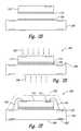
- FIG. 1is a partially schematic, cross-sectional side view of a microfeature workpiece 110 that can be attached to a support member to form an assembly (e.g., a package) in accordance with an embodiment of the invention.
- the microfeature workpiece 110can have a first major surface 111 , a second major surface 112 facing generally opposite from the first major surface 111 , and an edge surface 113 between the first and second major surfaces 111 , 112 .
- the microfeature workpiece 110can include a microelectronic die that has been separated from a larger substrate, e.g., a semiconductor wafer.
- the microfeature workpiece 110can accordingly include internal microelectronic features and structures (not visible in FIG. 1 ) that are electrically coupled to workpiece bond pads 114 .
- the bond pads 114can provide for electrical communication between features and structures within the microfeature workpiece 110 , and components and structures external to the microfeature workpiece 110 .
- the microfeature workpiece 110can include a first adhesive 115 adhesively attached to the second surface 112 , and configured to bond the microfeature workpiece 110 to a support member.
- the first adhesive 115can include a wafer backside laminate (WBL) that is applied to the microfeature workpiece 110 at the wafer level (e.g., before the microfeature workpiece 110 is separated or diced from a larger wafer or other substrate).
- WBLwafer backside laminate
- a sheet of the first adhesive 115can initially be carried by a dicing frame and attached to a wafer.
- the wafer attachment processcan occur at an elevated temperature (e.g., 40° C.-80° C.) and/or pressure (e.g., 20-50 psi).
- the first adhesive 115can include a film substrate having adhesive material attached to both opposing surfaces of the film (e.g., a double-backed adhesive film).
- the first adhesive 115can be a monolayer, e.g., a single layer of adhesive applied to the second surface 112 of the microfeature workpiece 110 .
- Suitable first adhesivesare available from Ablestick Laboratories of Collinso Dominguez, Calif. under part number RP787-3DS, and from the Hitachi Chemical Company Ltd. of Tokyo, Japan under part number FH-800.
- the first adhesive 115can act not only to adhere the microfeature workpiece 110 to a support member, but also to stiffen the microfeature workpiece 110 .
- the microfeature workpiece 110can be less likely to break during normal handling operations. This can be particularly important for very thin microfeature workpieces 110 , which may be more susceptible to such breakage.
- Such microfeature workpieces 110can have a thickness of 150 microns or less, e.g., 100 microns or less.
- FIGS. 2A-2Fillustrate a support member 220 and a method for attaching the support member 220 to the microfeature workpiece 110 described above with reference to FIG. 1 .
- the support member 220can include a printed circuit board or other suitable structure having provisions for electrical connections to the microfeature workpiece 110 ( FIG. 1 ).
- the support member 220can include first bond pads 221 at a first surface 227 , second bond pads 222 at an opposite, second surface 228 , and internal conductive structures (not visible in FIG. 2A ) coupling the first bond pads 221 to the second bond pads 222 .
- a stencil 223can be positioned adjacent to the first surface 227 .
- the stencil 223can include one or more openings 224 sized in accordance with the desired attachment surface area between the support member 220 and the microfeature workpiece 110 .
- a second adhesive 225can be applied to the support member 220 in a stenciling process. Accordingly, the second adhesive 225 can be distributed over the stencil 223 using techniques well-known to those of ordinary skill in the relevant art to fill the opening 224 .
- the second adhesive 225can include an epoxy that is applied to the support member 220 when in a liquid or otherwise generally flowable state. Accordingly, the second adhesive 225 can readily fill the opening 224 in the stencil 223 .
- the second adhesive 225can also readily fill gaps, recesses, projections, roughness elements, and/or other surface features 229 in the first surface 227 of the support member 220 . As a result, the second adhesive 225 can be in intimate contact with the surface features 229 to provide a robust bond with the support member 220 .
- the stencil 223is removed and the second adhesive 225 can be partially cured.
- the process of partially curing the second adhesive 225can include applying heat 226 and, optionally, pressure, to the second adhesive 225 .
- the temperature of the second adhesivecan be elevated to about 100° C. for about one hour, at atmospheric pressure, in an inert (e.g., nitrogen) environment.
- the partial curing process shown in FIG. 2Ccan include forming a B-stage epoxy.
- the term “B-stage”includes, but is not necessarily limited to, an intermediate stage in the reaction of a thermosetting resin in which the material softens when heated and swells when in contact with certain liquids, but does not entirely fuse or dissolve.
- the second adhesive 225is generally non-tacky (e.g., tack-free).
- Suitable epoxiesinclude Sumitomo X2225 available from Sumitomo Electric Industries, Ltd. of Osaka, Japan, and Ablestik RP809-1A available from Ablestik Laboratories of Rancho Dominguez, Calif.
- the microfeature workpiece 110can be positioned proximate to the support member 220 , with the first adhesive 115 of the microfeature workpiece 110 facing toward the second adhesive 225 of the support member 220 .
- the microfeature workpiece 110 and the support member 220can be moved toward each other so that the first adhesive 115 contacts the second adhesive 225 .
- the local temperaturecan be elevated (e.g., up to 100° C.-150° C.) for 1-3 seconds to “re-tack” the first and second adhesives 115 , 125 .
- the local pressurecan also be elevated (e.g., by from about 1 g/mm 2 to about 8 g/cm 2 ) in a standard air environment.
- FIG. 2Eillustrates the microfeature workpiece 110 with its first adhesive 115 contacting the second adhesive 225 of the support member 220 .
- the second adhesive 225can be fully cured by applying heat 226 (and optionally, pressure) to the second adhesive 225 to form an adhesive assembly 230 that includes both the first adhesive 115 and the second adhesive 225 .
- the adhesive assemblycan be cured at 100° C.-150° C. for 1-2 hours in an inert environment.
- the resulting combination of the microfeature workpiece 110 , the support member 220 , and the adhesive assembly 230forms an overall assembly or system 200 (e.g., a microfeature package).
- the assembly 200can include electrical couplings between the microfeature workpiece 110 and the support member 220 .
- the assembly 200can include wirebonds 201 extending between the workpiece bond pads 114 and the first bond pads 221 of the support member 220 .
- the assembly 200can optionally include an encapsulant 202 that at least partially surrounds the microfeature workpiece 110 and the wirebonds 201 or other electrical couplings between the microfeature workpiece 110 and the support member 220 .
- the completed assembly 200can be electrically coupled to other components via the second bond pads 222 located at the second surface 228 of the support member 220 .
- One feature of embodiments of the assembly 200 described above with reference to FIGS. 1-2Fis that they can include multiple adhesives.
- a further particular feature of at least some of these embodimentsis that an adhesive having a first composition can be positioned adjacent to the microfeature workpiece 110 , and an adhesive having a second, different composition can be positioned adjacent to the support member 220 .
- This combination of adhesivescan provide one or more of several advantages.
- the first adhesive 115can stiffen and strengthen the microfeature workpiece 110 and can accordingly reduce or eliminate the tendency for the microfeature workpiece 110 to warp, chip, and/or deform in other manners.
- Preventing the microfeature workpiece 110 from warpingcan be particularly important for workpieces 110 having high aspect ratios, e.g., about 4:1, 5:1 or up to 10:1.
- the second adhesive 225can more readily fill in the surface features 229 of the support member 220 . Accordingly, the second adhesive can be less likely to leave air voids or other imperfections that may reduce the bond strength between the second adhesive 225 and the support member 220 .
- each of the adhesive layerscan have a generally uniform thickness.
- the first adhesive 115can have the form of a generally uniform film.
- the second adhesive 225can be applied with a generally uniform thickness by using the stencil 223 . Because each adhesive layer has a generally uniform thickness, the microfeature workpiece 110 will be less likely to be tilted relative to the support member 220 .
- An advantage of this arrangementis that it can reduce the likelihood for the microfeature workpiece 110 (and/or the wirebonds 201 ) to be exposed through the encapsulant 202 as a result of the microfeature workpiece 110 being tilted or otherwise misaligned relative to the support member 220 .
- the adhesive assembly 230can be attached directly between the support member 240 and the second surface 112 of the microfeature workpiece 110 , without extending along the edge surfaces 113 of the microfeature workpiece 110 .
- An advantage of this “fillet-less” arrangementis that the adhesive assembly 230 may be less likely to subject the edge surfaces 113 of the microfeature workpiece 110 to stresses that can crack or otherwise damage the microfeature workpiece 110 .
- the adhesive assembly 230formed from adhesives having different chemical constituencies, can form a tight bond with both the microfeature workpiece 110 and the support member 220 .
- the failure mode of the adhesive assembly 230can be cohesive rather than adhesive.
- the adhesive assembly 230can fail internally rather than at the interfaces between the adhesive assembly 230 and either the microfeature workpiece 110 or the support member 220 . Because higher stresses are typically required for failure in the cohesive mode than in the adhesive mode, the overall strength of the bond between the support member 220 and the microfeature workpiece 110 can be greater than it is for existing adhesive arrangements.
- the adhesive assembly 230can produce a bond that more readily withstands typical moisture sensitivity testing environments. Such environments typically include transitions in temperature up to about 260° C., and an elevated humidity. Improved moisture sensitivity can also result in lower package stresses in challenging environmental conditions. As a result of any of the foregoing features, the package 200 can be more robust than existing packages, and can accordingly be more reliable in a wider variety of applications.
- a microfeature workpiece assembly 300can include a microfeature workpiece 310 having centrally located workpiece bond pads 314 in accordance with another embodiment of the invention.
- a corresponding support member 320can include an aperture 331 aligned with the workpiece bond pads 314 .
- the first adhesive 115can be positioned adjacent to the microfeature workpiece 310 (outwardly from the workpiece bond pads 314 ), and the second adhesive 225 can be positioned adjacent to the support member 320 (outwardly from the aperture 331 ).
- the microfeature workpiece 310can be bonded to the support member 320 using a second curing process.
- the workpiece bond pads 314can then be electrically coupled (e.g., with wirebonds 301 ) to first bond pads 321 of the support member 320 .
- the resulting connectioncan be at least partially surrounded with an encapsulant 302 .
- the first bond pads 321can be electrically coupled to second bond pads 322 , which can in turn provide communication with other devices, for example, via solder balls 303 .
- FIG. 4illustrates a microfeature workpiece package or assembly 400 that includes two microfeature workpieces 410 , shown as a first microfeature workpiece 410 a and a second microfeature workpiece 410 b.
- the first microfeature workpiece 410 acan be adhesively secured to a support member 420 with a first adhesive assembly 430 a.
- the first adhesive assembly 430 acan include a first adhesive 115 and a second adhesive 225 , configured in a manner generally similar to that described above.
- the second microfeature workpiece 410 bcan be adhered directly to the first microfeature workpiece 410 a with a second adhesive assembly 430 b that also includes a portion of the first adhesive 115 and the second adhesive 225 .
- First wirebonds 401 acan electrically couple the first microfeature workpiece 410 a to the support member 420
- second wirebonds 401 bcan electrically couple the second microfeature workpiece 410 b to the support member 420 .
- the entire package 400can be surrounded by an encapsulant 402 .
- the first microfeature workpiece 410 acan have a configuration generally similar to that of the second microfeature workpiece 410 b, and the second microfeature workpiece 410 b can overhang the first microfeature workpiece 410 a to allow for electrical coupling to both microfeature workpieces.
- multiple microfeature workpiecescan be stacked in other configurations.
- a package 500can include a first microfeature workpiece 510 a and a second, smaller microfeature workpiece 510 b, stacked upon the first microfeature workpiece 510 a.
- the first microfeature workpiece 510 acan be secured to a support member 520 with a first adhesive assembly 530 a
- the second microfeature workpiece 510 bcan be secured to the first microfeature workpiece 510 a with a second adhesive assembly 530 b.
- Each adhesive assembly 530 a, 530 bcan include the first adhesive 115 and the second adhesive 225 .
- arrangements generally similar to those described abovecan be used to attach one or more microfeature workpieces to corresponding support members and/or other microfeature workpieces.
- the microfeature workpiececan be electrically coupled to a corresponding support member with an electrical link other than a wirebond.
- aspects of the invention described in the context of particular embodimentsmay be combined or eliminated in other embodiments.
- advantages associated with certain embodiments of the inventionhave been described in the context of those embodiments, other embodiments may also exhibit such advantages.
- none of the foregoing embodimentsneed necessarily exhibit such advantages to fall within the scope of the invention. Accordingly, the invention is not limited except as by the appended claims.
Landscapes
- Engineering & Computer Science (AREA)
- Microelectronics & Electronic Packaging (AREA)
- Computer Hardware Design (AREA)
- Power Engineering (AREA)
- Manufacturing & Machinery (AREA)
- Physics & Mathematics (AREA)
- Condensed Matter Physics & Semiconductors (AREA)
- General Physics & Mathematics (AREA)
- Adhesives Or Adhesive Processes (AREA)
- Micromachines (AREA)
Abstract
Description
- The present invention relates generally to methods and systems for adhering microfeature workpieces to support members.
- Packaged microelectronics assemblies, such as memory chips and microprocessor chips, typically include a microelectronic die mounted to a substrate and encased in a plastic protective covering. The die includes functional features, such as memory cells, processor circuits and interconnecting circuitry. The die also typically includes bond pads electrically coupled to the functional features. The bond pads are electrically connected to pins or other types of terminals that extend outside the protective covering for connecting the die to buses, circuits, and/or other microelectronic assemblies.
- In one conventional arrangement, the die is mounted to a supporting substrate (e.g., a printed circuit board), and the die bond pads are electrically coupled to corresponding bond pads of the substrate with wire bonds. After encapsulation, the substrate can be electrically connected to external devices. Accordingly, the substrate supports the die and provides an electrical link between the die and the external devices.
- Prior to encapsulation, the microelectronic die is typically attached to the substrate with an adhesive. For example, one conventional assembly includes a wafer backside laminate (WBL) that adheres the microelectronic die to the substrate. Other assemblies include an epoxy that adheres the microelectronic die to the substrate. The foregoing adhesion techniques have both advantages and drawbacks. For example, a WBL generally increases the strength of the die, but does not fill in surface features on the substrate. Accordingly, the bond formed between the die and the substrate may fail due to an inadequate adhesive bond. Epoxies tend to flow more than WBLs do and can accordingly fill such features, but epoxies can fail in shear at the junction between the epoxy and the die, and/or at the junction between the epoxy and the substrate. Accordingly, it is desirable to adhere dies to substrates in a more robust manner.
FIG. 1 illustrates a microfeature workpiece having a first adhesive in accordance with an embodiment of the invention.FIGS. 2A-2F illustrate a process for manufacturing a microfeature workpiece assembly using first and second adhesives in accordance with an embodiment of the invention.FIG. 3 is a partially schematic illustration of a microfeature workpiece attached to a support member in accordance with another embodiment of the invention.FIG. 4 is a partially schematic illustration of a support member carrying two microfeature workpieces in accordance with another embodiment of the invention.FIG. 5 is a partially schematic illustration of a support member carrying two microfeature workpieces in accordance with still another embodiment of the invention.- The present invention relates generally to microfeature dies and methods for adhering such dies to support members, for example, printed circuit boards. A method for attaching a microfeature workpiece to a support member in accordance with one aspect of the invention includes disposing a first adhesive on a surface of the microfeature workpiece and disposing a second adhesive on a surface of the support member. The method can further include adhesively attaching the microfeature workpiece to the support member by contacting the first adhesive with the second adhesive while the second adhesive is only partially cured. For example, the method can include attaching a film adhesive to the microfeature workpiece, and stenciling a liquid epoxy on the support member. The method can further include partially curing the epoxy (for example, to B-stage) before attaching the microfeature workpiece to the support member by contacting the two adhesives with each other. The method can include further curing the second adhesive to complete the bond between the microfeature workpiece and the support member.
- In particular embodiments, the microfeature workpiece can have a first major surface, a second major surface facing opposite from the first major surface, and an edge surface between the first and second major surfaces. The method can further comprise electrically coupling the support member to the microfeature workpiece at the second major surface of the workpiece. In still a further aspect of the invention, the microfeature workpiece can be attached to the support member without either the first adhesive or the second adhesive contacting the edge surface of the microfeature workpiece.
- A method in accordance with another aspect of the invention includes stiffening a microfeature workpiece by disposing a first adhesive layer on a surface of the microfeature workpiece, with the first adhesive layer having a first composition. The method can further include filling voids in a surface of a support member by disposing a second adhesive layer on a surface of the support member, with the second adhesive layer having a second composition different than the first composition. The method can still further include adhesively attaching the microfeature workpiece to the support member by contacting the first adhesive layer with the second adhesive layer.
- Other aspects of the invention are directed toward microfeature workpiece systems or assemblies. A system in accordance with one aspect of the invention includes a microfeature workpiece having a first major surface, a second major surface facing away from the first major surface, and an edge surface between the first and second major surfaces. The system can further include a support member positioned adjacent to the microfeature workpiece, and an adhesive assembly attached between the microfeature workpiece and the support member. The adhesive assembly can include a first layer having a first composition and a first generally uniform thickness, and a second layer having a second composition different than the first with a second generally uniform thickness. In further specific aspects, the adhesive assembly can be generally out of contact with the edge surface of the microfeature workpiece, and the microfeature workpiece can be electrically coupled to the support member with an electrical coupling connected between the support member and the second major surface of the microfeature workpiece.
FIG. 1 is a partially schematic, cross-sectional side view of amicrofeature workpiece 110 that can be attached to a support member to form an assembly (e.g., a package) in accordance with an embodiment of the invention. Themicrofeature workpiece 110 can have a firstmajor surface 111, a secondmajor surface 112 facing generally opposite from the firstmajor surface 111, and anedge surface 113 between the first and secondmajor surfaces microfeature workpiece 110 can include a microelectronic die that has been separated from a larger substrate, e.g., a semiconductor wafer. Themicrofeature workpiece 110 can accordingly include internal microelectronic features and structures (not visible inFIG. 1 ) that are electrically coupled toworkpiece bond pads 114. Thebond pads 114 can provide for electrical communication between features and structures within themicrofeature workpiece 110, and components and structures external to themicrofeature workpiece 110.- The
microfeature workpiece 110 can include a first adhesive115 adhesively attached to thesecond surface 112, and configured to bond themicrofeature workpiece 110 to a support member. In one embodiment, thefirst adhesive 115 can include a wafer backside laminate (WBL) that is applied to themicrofeature workpiece 110 at the wafer level (e.g., before themicrofeature workpiece 110 is separated or diced from a larger wafer or other substrate). For example, a sheet of thefirst adhesive 115 can initially be carried by a dicing frame and attached to a wafer. The wafer attachment process can occur at an elevated temperature (e.g., 40° C.-80° C.) and/or pressure (e.g., 20-50 psi). After dicing the wafer, a small portion of the first adhesive115 remains attached to eachmicrofeature workpiece 110, and a standard pick and place process can be used to move themicrofeature workpiece 110. Thefirst adhesive 115 can include a film substrate having adhesive material attached to both opposing surfaces of the film (e.g., a double-backed adhesive film). In another embodiment, thefirst adhesive 115 can be a monolayer, e.g., a single layer of adhesive applied to thesecond surface 112 of themicrofeature workpiece 110. Suitable first adhesives are available from Ablestick Laboratories of Rancho Dominguez, Calif. under part number RP787-3DS, and from the Hitachi Chemical Company Ltd. of Tokyo, Japan under part number FH-800. - The
first adhesive 115 can act not only to adhere themicrofeature workpiece 110 to a support member, but also to stiffen themicrofeature workpiece 110. As a result, themicrofeature workpiece 110 can be less likely to break during normal handling operations. This can be particularly important for verythin microfeature workpieces 110, which may be more susceptible to such breakage.Such microfeature workpieces 110 can have a thickness of 150 microns or less, e.g., 100 microns or less. FIGS. 2A-2F illustrate asupport member 220 and a method for attaching thesupport member 220 to themicrofeature workpiece 110 described above with reference toFIG. 1 . Beginning withFIG. 2A , thesupport member 220 can include a printed circuit board or other suitable structure having provisions for electrical connections to the microfeature workpiece110 (FIG. 1 ). For example, thesupport member 220 can includefirst bond pads 221 at afirst surface 227,second bond pads 222 at an opposite,second surface 228, and internal conductive structures (not visible inFIG. 2A ) coupling thefirst bond pads 221 to thesecond bond pads 222. In preparation for applying an adhesive to thesupport member 220, astencil 223 can be positioned adjacent to thefirst surface 227. Thestencil 223 can include one ormore openings 224 sized in accordance with the desired attachment surface area between thesupport member 220 and themicrofeature workpiece 110.- Referring next to
FIG. 2B , asecond adhesive 225 can be applied to thesupport member 220 in a stenciling process. Accordingly, thesecond adhesive 225 can be distributed over thestencil 223 using techniques well-known to those of ordinary skill in the relevant art to fill theopening 224. In one aspect of this embodiment, thesecond adhesive 225 can include an epoxy that is applied to thesupport member 220 when in a liquid or otherwise generally flowable state. Accordingly, thesecond adhesive 225 can readily fill theopening 224 in thestencil 223. Thesecond adhesive 225 can also readily fill gaps, recesses, projections, roughness elements, and/or other surface features229 in thefirst surface 227 of thesupport member 220. As a result, thesecond adhesive 225 can be in intimate contact with the surface features229 to provide a robust bond with thesupport member 220. - In
FIG. 2C , thestencil 223 is removed and thesecond adhesive 225 can be partially cured. The process of partially curing thesecond adhesive 225 can include applyingheat 226 and, optionally, pressure, to thesecond adhesive 225. For example, the temperature of the second adhesive can be elevated to about 100° C. for about one hour, at atmospheric pressure, in an inert (e.g., nitrogen) environment. When thesecond adhesive 225 includes an epoxy, the partial curing process shown inFIG. 2C can include forming a B-stage epoxy. As used herein, the term “B-stage” includes, but is not necessarily limited to, an intermediate stage in the reaction of a thermosetting resin in which the material softens when heated and swells when in contact with certain liquids, but does not entirely fuse or dissolve. In this stage, thesecond adhesive 225 is generally non-tacky (e.g., tack-free). Suitable epoxies include Sumitomo X2225 available from Sumitomo Electric Industries, Ltd. of Osaka, Japan, and Ablestik RP809-1A available from Ablestik Laboratories of Rancho Dominguez, Calif. - Referring next to
FIG. 2D , themicrofeature workpiece 110 can be positioned proximate to thesupport member 220, with thefirst adhesive 115 of themicrofeature workpiece 110 facing toward thesecond adhesive 225 of thesupport member 220. Themicrofeature workpiece 110 and thesupport member 220 can be moved toward each other so that the first adhesive115 contacts thesecond adhesive 225. The local temperature can be elevated (e.g., up to 100° C.-150° C.) for 1-3 seconds to “re-tack” the first andsecond adhesives 115,125. The local pressure can also be elevated (e.g., by from about 1 g/mm2to about 8 g/cm2) in a standard air environment.FIG. 2E illustrates themicrofeature workpiece 110 with itsfirst adhesive 115 contacting thesecond adhesive 225 of thesupport member 220. At this point, thesecond adhesive 225 can be fully cured by applying heat226 (and optionally, pressure) to thesecond adhesive 225 to form anadhesive assembly 230 that includes both thefirst adhesive 115 and thesecond adhesive 225. In one embodiment, the adhesive assembly can be cured at 100° C.-150° C. for 1-2 hours in an inert environment. The resulting combination of themicrofeature workpiece 110, thesupport member 220, and theadhesive assembly 230 forms an overall assembly or system200 (e.g., a microfeature package). - Referring next to
FIG. 2F , theassembly 200 can include electrical couplings between themicrofeature workpiece 110 and thesupport member 220. For example, theassembly 200 can includewirebonds 201 extending between theworkpiece bond pads 114 and thefirst bond pads 221 of thesupport member 220. Theassembly 200 can optionally include anencapsulant 202 that at least partially surrounds themicrofeature workpiece 110 and thewirebonds 201 or other electrical couplings between themicrofeature workpiece 110 and thesupport member 220. The completedassembly 200 can be electrically coupled to other components via thesecond bond pads 222 located at thesecond surface 228 of thesupport member 220. - One feature of embodiments of the
assembly 200 described above with reference toFIGS. 1-2F is that they can include multiple adhesives. A further particular feature of at least some of these embodiments is that an adhesive having a first composition can be positioned adjacent to themicrofeature workpiece 110, and an adhesive having a second, different composition can be positioned adjacent to thesupport member 220. This combination of adhesives can provide one or more of several advantages. For example, thefirst adhesive 115 can stiffen and strengthen themicrofeature workpiece 110 and can accordingly reduce or eliminate the tendency for themicrofeature workpiece 110 to warp, chip, and/or deform in other manners. Preventing themicrofeature workpiece 110 from warping can be particularly important forworkpieces 110 having high aspect ratios, e.g., about 4:1, 5:1 or up to 10:1. Thesecond adhesive 225, on the other hand, can more readily fill in the surface features229 of thesupport member 220. Accordingly, the second adhesive can be less likely to leave air voids or other imperfections that may reduce the bond strength between thesecond adhesive 225 and thesupport member 220. - Another feature of at least some of the foregoing embodiments is that each of the adhesive layers can have a generally uniform thickness. For example, the
first adhesive 115 can have the form of a generally uniform film. Thesecond adhesive 225 can be applied with a generally uniform thickness by using thestencil 223. Because each adhesive layer has a generally uniform thickness, themicrofeature workpiece 110 will be less likely to be tilted relative to thesupport member 220. An advantage of this arrangement is that it can reduce the likelihood for the microfeature workpiece110 (and/or the wirebonds201) to be exposed through theencapsulant 202 as a result of themicrofeature workpiece 110 being tilted or otherwise misaligned relative to thesupport member 220. - Another feature associated with of the generally uniform layer thicknesses described above is that the
adhesive assembly 230 can be attached directly between the support member240 and thesecond surface 112 of themicrofeature workpiece 110, without extending along the edge surfaces113 of themicrofeature workpiece 110. An advantage of this “fillet-less” arrangement is that theadhesive assembly 230 may be less likely to subject the edge surfaces113 of themicrofeature workpiece 110 to stresses that can crack or otherwise damage themicrofeature workpiece 110. - Still another advantage of at least some of the foregoing embodiments is that the
adhesive assembly 230, formed from adhesives having different chemical constituencies, can form a tight bond with both themicrofeature workpiece 110 and thesupport member 220. When subjected to excessive stresses, the failure mode of theadhesive assembly 230 can be cohesive rather than adhesive. For example, theadhesive assembly 230 can fail internally rather than at the interfaces between theadhesive assembly 230 and either themicrofeature workpiece 110 or thesupport member 220. Because higher stresses are typically required for failure in the cohesive mode than in the adhesive mode, the overall strength of the bond between thesupport member 220 and themicrofeature workpiece 110 can be greater than it is for existing adhesive arrangements. - Yet another feature of the foregoing embodiments is that the
adhesive assembly 230 can produce a bond that more readily withstands typical moisture sensitivity testing environments. Such environments typically include transitions in temperature up to about 260° C., and an elevated humidity. Improved moisture sensitivity can also result in lower package stresses in challenging environmental conditions. As a result of any of the foregoing features, thepackage 200 can be more robust than existing packages, and can accordingly be more reliable in a wider variety of applications. - Methods and adhesive assemblies at least generally similar to those described above with reference to
FIGS. 1-2F can be used to bond microfeature workpieces to support members in other configurations as well. Referring now toFIG. 3 , amicrofeature workpiece assembly 300 can include amicrofeature workpiece 310 having centrally locatedworkpiece bond pads 314 in accordance with another embodiment of the invention. Acorresponding support member 320 can include anaperture 331 aligned with theworkpiece bond pads 314. Thefirst adhesive 115 can be positioned adjacent to the microfeature workpiece310 (outwardly from the workpiece bond pads314), and thesecond adhesive 225 can be positioned adjacent to the support member320 (outwardly from the aperture331). After thesecond adhesive 225 has been partially cured, themicrofeature workpiece 310 can be bonded to thesupport member 320 using a second curing process. Theworkpiece bond pads 314 can then be electrically coupled (e.g., with wirebonds301) tofirst bond pads 321 of thesupport member 320. The resulting connection can be at least partially surrounded with anencapsulant 302. Thefirst bond pads 321 can be electrically coupled tosecond bond pads 322, which can in turn provide communication with other devices, for example, viasolder balls 303. FIG. 4 illustrates a microfeature workpiece package orassembly 400 that includes two microfeature workpieces410, shown as afirst microfeature workpiece 410aand asecond microfeature workpiece 410b.Thefirst microfeature workpiece 410acan be adhesively secured to asupport member 420 with a firstadhesive assembly 430a.The firstadhesive assembly 430acan include afirst adhesive 115 and asecond adhesive 225, configured in a manner generally similar to that described above. Thesecond microfeature workpiece 410bcan be adhered directly to thefirst microfeature workpiece 410awith a secondadhesive assembly 430bthat also includes a portion of thefirst adhesive 115 and thesecond adhesive 225.First wirebonds 401acan electrically couple thefirst microfeature workpiece 410ato thesupport member 420, andsecond wirebonds 401bcan electrically couple thesecond microfeature workpiece 410bto thesupport member 420. Theentire package 400 can be surrounded by anencapsulant 402.- In one aspect of an embodiment shown in
FIG. 4 , thefirst microfeature workpiece 410acan have a configuration generally similar to that of thesecond microfeature workpiece 410b,and thesecond microfeature workpiece 410bcan overhang thefirst microfeature workpiece 410ato allow for electrical coupling to both microfeature workpieces. In other embodiments, multiple microfeature workpieces can be stacked in other configurations. For example, referring now toFIG. 5 , apackage 500 can include afirst microfeature workpiece 510aand a second,smaller microfeature workpiece 510b,stacked upon thefirst microfeature workpiece 510a.This arrangement allowsbond pads 514 on the outer edges of each microfeature workpiece510 to remain exposed despite the adhesive connection between the two microfeature workpieces. Thefirst microfeature workpiece 510acan be secured to asupport member 520 with a firstadhesive assembly 530a,and thesecond microfeature workpiece 510bcan be secured to thefirst microfeature workpiece 510awith a secondadhesive assembly 530b.Eachadhesive assembly first adhesive 115 and thesecond adhesive 225. In other embodiments, arrangements generally similar to those described above can be used to attach one or more microfeature workpieces to corresponding support members and/or other microfeature workpieces. - From the foregoing, it will be appreciated that specific embodiments of the invention have been described herein for purposes of illustration, but that various modifications may be made without deviating from the spirit and scope of the invention. For example, the microfeature workpiece can be electrically coupled to a corresponding support member with an electrical link other than a wirebond. Aspects of the invention described in the context of particular embodiments may be combined or eliminated in other embodiments. Although advantages associated with certain embodiments of the invention have been described in the context of those embodiments, other embodiments may also exhibit such advantages. Additionally, none of the foregoing embodiments need necessarily exhibit such advantages to fall within the scope of the invention. Accordingly, the invention is not limited except as by the appended claims.
Claims (22)
Priority Applications (2)
| Application Number | Priority Date | Filing Date | Title |
|---|---|---|---|
| US11/407,560US7518237B2 (en) | 2005-02-08 | 2006-04-19 | Microfeature systems including adhered microfeature workpieces and support members |
| US13/611,509US9064973B2 (en) | 2005-02-08 | 2012-09-12 | Die attached to a support member by a plurality of adhesive members |
Applications Claiming Priority (2)
| Application Number | Priority Date | Filing Date | Title |
|---|---|---|---|
| US11/053,984US8278751B2 (en) | 2005-02-08 | 2005-02-08 | Methods of adhering microfeature workpieces, including a chip, to a support member |
| US11/407,560US7518237B2 (en) | 2005-02-08 | 2006-04-19 | Microfeature systems including adhered microfeature workpieces and support members |
Related Parent Applications (1)
| Application Number | Title | Priority Date | Filing Date |
|---|---|---|---|
| US11/053,984DivisionUS8278751B2 (en) | 2005-02-08 | 2005-02-08 | Methods of adhering microfeature workpieces, including a chip, to a support member |
Publications (2)
| Publication Number | Publication Date |
|---|---|
| US20060189036A1true US20060189036A1 (en) | 2006-08-24 |
| US7518237B2 US7518237B2 (en) | 2009-04-14 |
Family
ID=36780481
Family Applications (3)
| Application Number | Title | Priority Date | Filing Date |
|---|---|---|---|
| US11/053,984Active2028-11-18US8278751B2 (en) | 2005-02-08 | 2005-02-08 | Methods of adhering microfeature workpieces, including a chip, to a support member |
| US11/407,560Expired - LifetimeUS7518237B2 (en) | 2005-02-08 | 2006-04-19 | Microfeature systems including adhered microfeature workpieces and support members |
| US13/611,509Expired - LifetimeUS9064973B2 (en) | 2005-02-08 | 2012-09-12 | Die attached to a support member by a plurality of adhesive members |
Family Applications Before (1)
| Application Number | Title | Priority Date | Filing Date |
|---|---|---|---|
| US11/053,984Active2028-11-18US8278751B2 (en) | 2005-02-08 | 2005-02-08 | Methods of adhering microfeature workpieces, including a chip, to a support member |
Family Applications After (1)
| Application Number | Title | Priority Date | Filing Date |
|---|---|---|---|
| US13/611,509Expired - LifetimeUS9064973B2 (en) | 2005-02-08 | 2012-09-12 | Die attached to a support member by a plurality of adhesive members |
Country Status (1)
| Country | Link |
|---|---|
| US (3) | US8278751B2 (en) |
Cited By (8)
| Publication number | Priority date | Publication date | Assignee | Title |
|---|---|---|---|---|
| US20070020811A1 (en)* | 2002-04-04 | 2007-01-25 | Micron Technology, Inc. | Method and apparatus for attaching microelectronic substrates and support members |
| US20090111221A1 (en)* | 2007-10-31 | 2009-04-30 | Utac (Taiwan) Corporation | Fabrication method of semiconductor device |
| US20100127409A1 (en)* | 2008-11-26 | 2010-05-27 | Micron Technology, Inc. | Microelectronic device wafers including an in-situ molded adhesive, molds for in-situ molding adhesives on microelectronic device wafers, and methods of molding adhesives on microelectronic device wafers |
| US20120007256A1 (en)* | 2006-08-30 | 2012-01-12 | Micron Technology, Inc. | Redistribution layers for microfeature workpieces, and associated systems and methods |
| CN104517934A (en)* | 2013-09-27 | 2015-04-15 | 英特尔公司 | Method for interconnecting stacked semiconductor devices |
| US9064973B2 (en) | 2005-02-08 | 2015-06-23 | Micron Technology, Inc. | Die attached to a support member by a plurality of adhesive members |
| US20150325550A1 (en)* | 2013-09-27 | 2015-11-12 | Junfeng Zhao | Method for interconnecting stacked semiconductor devices |
| RU2664894C1 (en)* | 2017-08-14 | 2018-08-23 | Интел Корпорейшн | Method of connecting multilevel semiconductor devices |
Families Citing this family (4)
| Publication number | Priority date | Publication date | Assignee | Title |
|---|---|---|---|---|
| US20070026573A1 (en)* | 2005-07-28 | 2007-02-01 | Aminuddin Ismail | Method of making a stacked die package |
| KR101195460B1 (en) | 2010-01-06 | 2012-10-30 | 에스케이하이닉스 주식회사 | Stacked semiconductor package |
| JP4825919B1 (en)* | 2010-05-31 | 2011-11-30 | 株式会社東芝 | Electronics |
| TWI575779B (en)* | 2014-03-31 | 2017-03-21 | 精材科技股份有限公司 | Chip package and method for forming the same |
Citations (88)
| Publication number | Priority date | Publication date | Assignee | Title |
|---|---|---|---|---|
| US4563811A (en)* | 1983-10-28 | 1986-01-14 | At&T Technologies, Inc. | Method of making a dual-in-line package |
| US5128831A (en)* | 1991-10-31 | 1992-07-07 | Micron Technology, Inc. | High-density electronic package comprising stacked sub-modules which are electrically interconnected by solder-filled vias |
| US5139973A (en)* | 1990-12-17 | 1992-08-18 | Allegro Microsystems, Inc. | Method for making a semiconductor package with the distance between a lead frame die pad and heat spreader determined by the thickness of an intermediary insulating sheet |
| US5208188A (en)* | 1989-10-02 | 1993-05-04 | Advanced Micro Devices, Inc. | Process for making a multilayer lead frame assembly for an integrated circuit structure and multilayer integrated circuit die package formed by such process |
| US5518957A (en)* | 1991-10-10 | 1996-05-21 | Samsung Electronics Co., Ltd. | Method for making a thin profile semiconductor package |
| US5535101A (en)* | 1992-11-03 | 1996-07-09 | Motorola, Inc. | Leadless integrated circuit package |
| US5593927A (en)* | 1993-10-14 | 1997-01-14 | Micron Technology, Inc. | Method for packaging semiconductor dice |
| US5614766A (en)* | 1991-09-30 | 1997-03-25 | Rohm Co., Ltd. | Semiconductor device with stacked alternate-facing chips |
| US5656857A (en)* | 1994-05-12 | 1997-08-12 | Kabushiki Kaisha Toshiba | Semiconductor device with insulating resin layer and substrate having low sheet resistance |
| US5739585A (en)* | 1995-11-27 | 1998-04-14 | Micron Technology, Inc. | Single piece package for semiconductor die |
| USD394844S (en)* | 1997-04-25 | 1998-06-02 | Micron Technology, Inc. | Temporary package for semiconductor dice |
| US5855821A (en)* | 1995-12-22 | 1999-01-05 | Johnson Matthey, Inc. | Materials for semiconductor device assemblies |
| US5866953A (en)* | 1996-05-24 | 1999-02-02 | Micron Technology, Inc. | Packaged die on PCB with heat sink encapsulant |
| US5871808A (en)* | 1996-12-20 | 1999-02-16 | Mcms, Inc. | Method for preserving solder paste in the manufacturing of printed circuit board assemblies |
| US5883426A (en)* | 1996-04-18 | 1999-03-16 | Nec Corporation | Stack module |
| US5891753A (en)* | 1997-01-24 | 1999-04-06 | Micron Technology, Inc. | Method and apparatus for packaging flip chip bare die on printed circuit boards |
| US5893726A (en)* | 1997-12-15 | 1999-04-13 | Micron Technology, Inc. | Semiconductor package with pre-fabricated cover and method of fabrication |
| US5920118A (en)* | 1996-12-18 | 1999-07-06 | Hyundai Electronics Industries Co., Ltd. | Chip-size package semiconductor |
| US5925930A (en)* | 1996-05-21 | 1999-07-20 | Micron Technology, Inc. | IC contacts with palladium layer and flexible conductive epoxy bumps |
| US5933713A (en)* | 1998-04-06 | 1999-08-03 | Micron Technology, Inc. | Method of forming overmolded chip scale package and resulting product |
| US5938956A (en)* | 1996-09-10 | 1999-08-17 | Micron Technology, Inc. | Circuit and method for heating an adhesive to package or rework a semiconductor die |
| US5946553A (en)* | 1991-06-04 | 1999-08-31 | Micron Technology, Inc. | Process for manufacturing a semiconductor package with bi-substrate die |
| US6017776A (en)* | 1997-04-29 | 2000-01-25 | Micron Technology, Inc. | Method of attaching a leadframe to singulated semiconductor dice |
| US6020629A (en)* | 1998-06-05 | 2000-02-01 | Micron Technology, Inc. | Stacked semiconductor package and method of fabrication |
| US6025728A (en)* | 1997-04-25 | 2000-02-15 | Micron Technology, Inc. | Semiconductor package with wire bond protective member |
| US6028365A (en)* | 1998-03-30 | 2000-02-22 | Micron Technology, Inc. | Integrated circuit package and method of fabrication |
| US6046496A (en)* | 1997-11-04 | 2000-04-04 | Micron Technology Inc | Chip package |
| US6048744A (en)* | 1997-09-15 | 2000-04-11 | Micron Technology, Inc. | Integrated circuit package alignment feature |
| US6048755A (en)* | 1998-11-12 | 2000-04-11 | Micron Technology, Inc. | Method for fabricating BGA package using substrate with patterned solder mask open in die attach area |
| US6049125A (en)* | 1997-12-29 | 2000-04-11 | Micron Technology, Inc. | Semiconductor package with heat sink and method of fabrication |
| US6051878A (en)* | 1997-03-10 | 2000-04-18 | Micron Technology, Inc. | Method of constructing stacked packages |
| US6063647A (en)* | 1997-12-08 | 2000-05-16 | 3M Innovative Properties Company | Method for making circuit elements for a z-axis interconnect |
| US6072233A (en)* | 1998-05-04 | 2000-06-06 | Micron Technology, Inc. | Stackable ball grid array package |
| US6072236A (en)* | 1996-03-07 | 2000-06-06 | Micron Technology, Inc. | Micromachined chip scale package |
| US6075288A (en)* | 1998-06-08 | 2000-06-13 | Micron Technology, Inc. | Semiconductor package having interlocking heat sinks and method of fabrication |
| US6089920A (en)* | 1998-05-04 | 2000-07-18 | Micron Technology, Inc. | Modular die sockets with flexible interconnects for packaging bare semiconductor die |
| US6097087A (en)* | 1997-10-31 | 2000-08-01 | Micron Technology, Inc. | Semiconductor package including flex circuit, interconnects and dense array external contacts |
| US6103547A (en)* | 1997-01-17 | 2000-08-15 | Micron Technology, Inc. | High speed IC package configuration |
| US6107680A (en)* | 1995-01-04 | 2000-08-22 | Micron Technology, Inc. | Packaging for bare dice employing EMR-sensitive adhesives |
| US6107122A (en)* | 1997-08-04 | 2000-08-22 | Micron Technology, Inc. | Direct die contact (DDC) semiconductor package |
| US6172419B1 (en)* | 1998-02-24 | 2001-01-09 | Micron Technology, Inc. | Low profile ball grid array package |
| US6175149B1 (en)* | 1998-02-13 | 2001-01-16 | Micron Technology, Inc. | Mounting multiple semiconductor dies in a package |
| US6175159B1 (en)* | 1997-07-16 | 2001-01-16 | Oki Electric Industry Co., Ltd. | Semiconductor package |
| US6194250B1 (en)* | 1998-09-14 | 2001-02-27 | Motorola, Inc. | Low-profile microelectronic package |
| US6198172B1 (en)* | 1997-02-20 | 2001-03-06 | Micron Technology, Inc. | Semiconductor chip package |
| US6208519B1 (en)* | 1999-08-31 | 2001-03-27 | Micron Technology, Inc. | Thermally enhanced semiconductor package |
| US6210992B1 (en)* | 1999-08-31 | 2001-04-03 | Micron Technology, Inc. | Controlling packaging encapsulant leakage |
| US6215175B1 (en)* | 1998-07-06 | 2001-04-10 | Micron Technology, Inc. | Semiconductor package having metal foil die mounting plate |
| US6212767B1 (en)* | 1999-08-31 | 2001-04-10 | Micron Technology, Inc. | Assembling a stacked die package |
| US6218731B1 (en)* | 1999-05-21 | 2001-04-17 | Siliconware Precision Industries Co., Ltd. | Tiny ball grid array package |
| US6225689B1 (en)* | 1998-08-21 | 2001-05-01 | Micron Technology, Inc. | Low profile multi-IC chip package connector |
| US6229202B1 (en)* | 2000-01-10 | 2001-05-08 | Micron Technology, Inc. | Semiconductor package having downset leadframe for reducing package bow |
| US6228548B1 (en)* | 1998-02-27 | 2001-05-08 | Micron Technology, Inc. | Method of making a multichip semiconductor package |
| US6235554B1 (en)* | 1995-11-27 | 2001-05-22 | Micron Technology, Inc. | Method for fabricating stackable chip scale semiconductor package |
| US6259153B1 (en)* | 1998-08-20 | 2001-07-10 | Micron Technology, Inc. | Transverse hybrid LOC package |
| US6261865B1 (en)* | 1998-10-06 | 2001-07-17 | Micron Technology, Inc. | Multi chip semiconductor package and method of construction |
| US6271058B1 (en)* | 1998-01-06 | 2001-08-07 | Nec Corporation | Method of manufacturing semiconductor device in which semiconductor chip is mounted facedown on board |
| US6277671B1 (en)* | 1998-10-20 | 2001-08-21 | Micron Technology, Inc. | Methods of forming integrated circuit packages |
| US6281577B1 (en)* | 1996-06-28 | 2001-08-28 | Pac Tech-Packaging Technologies Gmbh | Chips arranged in plurality of planes and electrically connected to one another |
| US6342728B2 (en)* | 1996-03-22 | 2002-01-29 | Hitachi, Ltd. | Semiconductor device and manufacturing method thereof |
| US6365434B1 (en)* | 2000-06-28 | 2002-04-02 | Micron Technology, Inc. | Method and apparatus for reduced flash encapsulation of microelectronic devices |
| US6385049B1 (en)* | 2001-07-05 | 2002-05-07 | Walsin Advanced Electronics Ltd | Multi-board BGA package |
| US6396129B1 (en)* | 2001-03-05 | 2002-05-28 | Siliconware Precision Industries Co., Ltd. | Leadframe with dot array of silver-plated regions on die pad for use in exposed-pad semiconductor package |
| US6400033B1 (en)* | 2000-06-01 | 2002-06-04 | Amkor Technology, Inc. | Reinforcing solder connections of electronic devices |
| US20020074645A1 (en)* | 2000-06-09 | 2002-06-20 | Dickey Brenton L. | Pre-applied adhesion promoter |
| US6528408B2 (en)* | 2001-05-21 | 2003-03-04 | Micron Technology, Inc. | Method for bumped die and wire bonded board-on-chip package |
| US6528722B2 (en)* | 1998-07-31 | 2003-03-04 | Siliconware Precision Industries Co., Ltd. | Ball grid array semiconductor package with exposed base layer |
| US6541872B1 (en)* | 1999-01-11 | 2003-04-01 | Micron Technology, Inc. | Multi-layered adhesive for attaching a semiconductor die to a substrate |
| US6548376B2 (en)* | 2001-08-30 | 2003-04-15 | Micron Technology, Inc. | Methods of thinning microelectronic workpieces |
| US6548757B1 (en)* | 2000-08-28 | 2003-04-15 | Micron Technology, Inc. | Microelectronic device assemblies having a shielded input and methods for manufacturing and operating such microelectronic device assemblies |
| US6552910B1 (en)* | 2000-06-28 | 2003-04-22 | Micron Technology, Inc. | Stacked-die assemblies with a plurality of microelectronic devices and methods of manufacture |
| US6558600B1 (en)* | 2000-05-04 | 2003-05-06 | Micron Technology, Inc. | Method for packaging microelectronic substrates |
| US6560117B2 (en)* | 2000-06-28 | 2003-05-06 | Micron Technology, Inc. | Packaged microelectronic die assemblies and methods of manufacture |
| US6561479B1 (en)* | 2000-08-23 | 2003-05-13 | Micron Technology, Inc. | Small scale actuators and methods for their formation and use |
| US6564979B2 (en)* | 2001-07-18 | 2003-05-20 | Micron Technology, Inc. | Method and apparatus for dispensing adhesive on microelectronic substrate supports |
| US6576495B1 (en)* | 2000-08-30 | 2003-06-10 | Micron Technology, Inc. | Microelectronic assembly with pre-disposed fill material and associated method of manufacture |
| US6576494B1 (en)* | 2000-06-28 | 2003-06-10 | Micron Technology, Inc. | Recessed encapsulated microelectronic devices and methods for formation |
| US6589820B1 (en)* | 2000-06-16 | 2003-07-08 | Micron Technology, Inc. | Method and apparatus for packaging a microelectronic die |
| US6592783B2 (en)* | 2000-02-25 | 2003-07-15 | Sony Chemicals Corp. | Anisotropic conductive adhesive film |
| US20030134451A1 (en)* | 2002-01-14 | 2003-07-17 | Picta Technology, Inc. | Structure and process for packaging back-to-back chips |
| US6607937B1 (en)* | 2000-08-23 | 2003-08-19 | Micron Technology, Inc. | Stacked microelectronic dies and methods for stacking microelectronic dies |
| US6673649B1 (en)* | 2002-07-05 | 2004-01-06 | Micron Technology, Inc. | Microelectronic device packages and methods for controlling the disposition of non-conductive materials in such packages |
| US20040067606A1 (en)* | 2002-10-02 | 2004-04-08 | Fehr Gerald K. | Method for stack-packaging integrated circuit die using at least one die in the package as a spacer |
| US6724076B1 (en)* | 1999-11-15 | 2004-04-20 | Infineon Technologies Ag | Package for a semiconductor chip |
| US20050006743A1 (en)* | 2003-07-01 | 2005-01-13 | Kim Tae-Hyun | In-line apparatus and method for manufacturing double-sided stacked multi-chip packages |
| US6844618B2 (en)* | 2002-04-04 | 2005-01-18 | Micron Technology, Inc. | Microelectronic package with reduced underfill and methods for forming such packages |
| US20050019988A1 (en)* | 2002-04-04 | 2005-01-27 | Tongbi Jiang | Method and apparatus for attaching microelectronic substrates and support members |
| US6906424B2 (en)* | 2002-08-02 | 2005-06-14 | Micron Technology, Inc. | Semiconductor package and method producing same |
Family Cites Families (54)
| Publication number | Priority date | Publication date | Assignee | Title |
|---|---|---|---|---|
| USRE36469E (en) | 1988-09-30 | 1999-12-28 | Micron Technology, Inc. | Packaging for semiconductor logic devices |
| US5252857A (en) | 1991-08-05 | 1993-10-12 | International Business Machines Corporation | Stacked DCA memory chips |
| JP3404795B2 (en) | 1993-03-31 | 2003-05-12 | 東レ株式会社 | Epoxy resin composition for semiconductor encapsulation |
| US5958100A (en) | 1993-06-03 | 1999-09-28 | Micron Technology, Inc. | Process of making a glass semiconductor package |
| JPH07263382A (en)* | 1994-03-24 | 1995-10-13 | Kawasaki Steel Corp | Wafer fixing tape |
| US5677566A (en) | 1995-05-08 | 1997-10-14 | Micron Technology, Inc. | Semiconductor chip package |
| US5696033A (en) | 1995-08-16 | 1997-12-09 | Micron Technology, Inc. | Method for packaging a semiconductor die |
| US5691567A (en)* | 1995-09-19 | 1997-11-25 | National Semiconductor Corporation | Structure for attaching a lead frame to a heat spreader/heat slug structure |
| US5851845A (en) | 1995-12-18 | 1998-12-22 | Micron Technology, Inc. | Process for packaging a semiconductor die using dicing and testing |
| US5733800A (en) | 1996-05-21 | 1998-03-31 | Micron Technology, Inc. | Underfill coating for LOC package |
| JP3195236B2 (en) | 1996-05-30 | 2001-08-06 | 株式会社日立製作所 | Wiring tape having adhesive film, semiconductor device and manufacturing method |
| JP2870497B2 (en) | 1996-08-01 | 1999-03-17 | 日本電気株式会社 | Semiconductor element mounting method |
| USD402638S (en) | 1997-04-25 | 1998-12-15 | Micron Technology, Inc. | Temporary package for semiconductor dice |
| US5955777A (en) | 1997-07-02 | 1999-09-21 | Micron Technology, Inc. | Lead frame assemblies with voltage reference plane and IC packages including same |
| US6159764A (en) | 1997-07-02 | 2000-12-12 | Micron Technology, Inc. | Varied-thickness heat sink for integrated circuit (IC) packages and method of fabricating IC packages |
| US5986209A (en) | 1997-07-09 | 1999-11-16 | Micron Technology, Inc. | Package stack via bottom leaded plastic (BLP) packaging |
| US6114769A (en) | 1997-07-18 | 2000-09-05 | Mcms, Inc. | Solder paste brick |
| US5944199A (en) | 1997-11-25 | 1999-08-31 | Micron Technology, Inc. | Integrated circuit package support system |
| US5989941A (en) | 1997-12-12 | 1999-11-23 | Micron Technology, Inc. | Encapsulated integrated circuit packaging |
| US5994784A (en) | 1997-12-18 | 1999-11-30 | Micron Technology, Inc. | Die positioning in integrated circuit packaging |
| US6117382A (en) | 1998-02-05 | 2000-09-12 | Micron Technology, Inc. | Method for encasing array packages |
| US6297547B1 (en) | 1998-02-13 | 2001-10-02 | Micron Technology Inc. | Mounting multiple semiconductor dies in a package |
| US6314639B1 (en) | 1998-02-23 | 2001-11-13 | Micron Technology, Inc. | Chip scale package with heat spreader and method of manufacture |
| US6002165A (en) | 1998-02-23 | 1999-12-14 | Micron Technology, Inc. | Multilayered lead frame for semiconductor packages |
| US6501157B1 (en) | 1998-04-15 | 2002-12-31 | Micron Technology, Inc. | Substrate for accepting wire bonded or flip-chip components |
| US5990566A (en) | 1998-05-20 | 1999-11-23 | Micron Technology, Inc. | High density semiconductor package |
| US6008070A (en) | 1998-05-21 | 1999-12-28 | Micron Technology, Inc. | Wafer level fabrication and assembly of chip scale packages |
| JP2000156435A (en) | 1998-06-22 | 2000-06-06 | Fujitsu Ltd | Semiconductor device and manufacturing method thereof |
| US6291894B1 (en) | 1998-08-31 | 2001-09-18 | Micron Technology, Inc. | Method and apparatus for a semiconductor package for vertical surface mounting |
| US6326687B1 (en) | 1998-09-01 | 2001-12-04 | Micron Technology, Inc. | IC package with dual heat spreaders |
| US6515355B1 (en) | 1998-09-02 | 2003-02-04 | Micron Technology, Inc. | Passivation layer for packaged integrated circuits |
| US6084297A (en) | 1998-09-03 | 2000-07-04 | Micron Technology, Inc. | Cavity ball grid array apparatus |
| US6117797A (en) | 1998-09-03 | 2000-09-12 | Micron Technology, Inc. | Attachment method for heat sinks and devices involving removal of misplaced encapsulant |
| US6743319B2 (en)* | 1998-09-30 | 2004-06-01 | Paralec Inc. | Adhesiveless transfer lamination method and materials for producing electronic circuits |
| US6008074A (en) | 1998-10-01 | 1999-12-28 | Micron Technology, Inc. | Method of forming a synchronous-link dynamic random access memory edge-mounted device |
| US6303985B1 (en) | 1998-11-12 | 2001-10-16 | Micron Technology, Inc. | Semiconductor lead frame and package with stiffened mounting paddle |
| US6184465B1 (en) | 1998-11-12 | 2001-02-06 | Micron Technology, Inc. | Semiconductor package |
| US6455354B1 (en)* | 1998-12-30 | 2002-09-24 | Micron Technology, Inc. | Method of fabricating tape attachment chip-on-board assemblies |
| US6310390B1 (en) | 1999-04-08 | 2001-10-30 | Micron Technology, Inc. | BGA package and method of fabrication |
| US6118176A (en) | 1999-04-26 | 2000-09-12 | Advanced Semiconductor Engineering, Inc. | Stacked chip assembly utilizing a lead frame |
| US6709968B1 (en) | 2000-08-16 | 2004-03-23 | Micron Technology, Inc. | Microelectronic device with package with conductive elements and associated method of manufacture |
| US6670719B2 (en) | 1999-08-25 | 2003-12-30 | Micron Technology, Inc. | Microelectronic device package filled with liquid or pressurized gas and associated method of manufacture |
| US6448635B1 (en) | 1999-08-30 | 2002-09-10 | Amkor Technology, Inc. | Surface acoustical wave flip chip |
| US6294839B1 (en) | 1999-08-30 | 2001-09-25 | Micron Technology, Inc. | Apparatus and methods of packaging and testing die |
| US6303981B1 (en) | 1999-09-01 | 2001-10-16 | Micron Technology, Inc. | Semiconductor package having stacked dice and leadframes and method of fabrication |
| US6329220B1 (en) | 1999-11-23 | 2001-12-11 | Micron Technology, Inc. | Packages for semiconductor die |
| US6331453B1 (en) | 1999-12-16 | 2001-12-18 | Micron Technology, Inc. | Method for fabricating semiconductor packages using mold tooling fixture with flash control cavities |
| AU2001259681A1 (en) | 2000-05-08 | 2001-11-20 | Micron Technology, Inc. | Method and apparatus for distributing mold material in a mold for packaging microelectronic devices |
| US6326698B1 (en) | 2000-06-08 | 2001-12-04 | Micron Technology, Inc. | Semiconductor devices having protective layers thereon through which contact pads are exposed and stereolithographic methods of fabricating such semiconductor devices |
| WO2002058108A2 (en)* | 2000-11-14 | 2002-07-25 | Henkel Loctite Corporation | Wafer applied fluxing and underfill material, and layered electronic assemblies manufactured therewith |
| US6622380B1 (en) | 2002-02-12 | 2003-09-23 | Micron Technology, Inc. | Methods for manufacturing microelectronic devices and methods for mounting microelectronic packages to circuit boards |
| JP4275522B2 (en)* | 2003-12-26 | 2009-06-10 | 日東電工株式会社 | Dicing die bond film |
| US20050230821A1 (en)* | 2004-04-15 | 2005-10-20 | Kheng Lee T | Semiconductor packages, and methods of forming semiconductor packages |
| US8278751B2 (en) | 2005-02-08 | 2012-10-02 | Micron Technology, Inc. | Methods of adhering microfeature workpieces, including a chip, to a support member |
- 2005
- 2005-02-08USUS11/053,984patent/US8278751B2/enactiveActive
- 2006
- 2006-04-19USUS11/407,560patent/US7518237B2/ennot_activeExpired - Lifetime
- 2012
- 2012-09-12USUS13/611,509patent/US9064973B2/ennot_activeExpired - Lifetime
Patent Citations (99)
| Publication number | Priority date | Publication date | Assignee | Title |
|---|---|---|---|---|
| US4563811A (en)* | 1983-10-28 | 1986-01-14 | At&T Technologies, Inc. | Method of making a dual-in-line package |
| US5208188A (en)* | 1989-10-02 | 1993-05-04 | Advanced Micro Devices, Inc. | Process for making a multilayer lead frame assembly for an integrated circuit structure and multilayer integrated circuit die package formed by such process |
| US5139973A (en)* | 1990-12-17 | 1992-08-18 | Allegro Microsystems, Inc. | Method for making a semiconductor package with the distance between a lead frame die pad and heat spreader determined by the thickness of an intermediary insulating sheet |
| US5946553A (en)* | 1991-06-04 | 1999-08-31 | Micron Technology, Inc. | Process for manufacturing a semiconductor package with bi-substrate die |
| US6020624A (en)* | 1991-06-04 | 2000-02-01 | Micron Technology, Inc. | Semiconductor package with bi-substrate die |
| US5614766A (en)* | 1991-09-30 | 1997-03-25 | Rohm Co., Ltd. | Semiconductor device with stacked alternate-facing chips |
| US5518957A (en)* | 1991-10-10 | 1996-05-21 | Samsung Electronics Co., Ltd. | Method for making a thin profile semiconductor package |
| US5128831A (en)* | 1991-10-31 | 1992-07-07 | Micron Technology, Inc. | High-density electronic package comprising stacked sub-modules which are electrically interconnected by solder-filled vias |
| US5535101A (en)* | 1992-11-03 | 1996-07-09 | Motorola, Inc. | Leadless integrated circuit package |
| US5593927A (en)* | 1993-10-14 | 1997-01-14 | Micron Technology, Inc. | Method for packaging semiconductor dice |
| US5656857A (en)* | 1994-05-12 | 1997-08-12 | Kabushiki Kaisha Toshiba | Semiconductor device with insulating resin layer and substrate having low sheet resistance |
| US6107680A (en)* | 1995-01-04 | 2000-08-22 | Micron Technology, Inc. | Packaging for bare dice employing EMR-sensitive adhesives |
| US6235554B1 (en)* | 1995-11-27 | 2001-05-22 | Micron Technology, Inc. | Method for fabricating stackable chip scale semiconductor package |
| US5739585A (en)* | 1995-11-27 | 1998-04-14 | Micron Technology, Inc. | Single piece package for semiconductor die |
| US5855821A (en)* | 1995-12-22 | 1999-01-05 | Johnson Matthey, Inc. | Materials for semiconductor device assemblies |
| US6072236A (en)* | 1996-03-07 | 2000-06-06 | Micron Technology, Inc. | Micromachined chip scale package |
| US6342728B2 (en)* | 1996-03-22 | 2002-01-29 | Hitachi, Ltd. | Semiconductor device and manufacturing method thereof |
| US5883426A (en)* | 1996-04-18 | 1999-03-16 | Nec Corporation | Stack module |
| US5925930A (en)* | 1996-05-21 | 1999-07-20 | Micron Technology, Inc. | IC contacts with palladium layer and flexible conductive epoxy bumps |
| US6252308B1 (en)* | 1996-05-24 | 2001-06-26 | Micron Technology, Inc. | Packaged die PCB with heat sink encapsulant |
| US5866953A (en)* | 1996-05-24 | 1999-02-02 | Micron Technology, Inc. | Packaged die on PCB with heat sink encapsulant |
| US6281577B1 (en)* | 1996-06-28 | 2001-08-28 | Pac Tech-Packaging Technologies Gmbh | Chips arranged in plurality of planes and electrically connected to one another |
| US5938956A (en)* | 1996-09-10 | 1999-08-17 | Micron Technology, Inc. | Circuit and method for heating an adhesive to package or rework a semiconductor die |
| US5920118A (en)* | 1996-12-18 | 1999-07-06 | Hyundai Electronics Industries Co., Ltd. | Chip-size package semiconductor |
| US5871808A (en)* | 1996-12-20 | 1999-02-16 | Mcms, Inc. | Method for preserving solder paste in the manufacturing of printed circuit board assemblies |
| US5876498A (en)* | 1996-12-20 | 1999-03-02 | Moms, Inc. | Apparatus for preserving solder paste in the manufacturing of printed circuit board assemblies |
| US6103547A (en)* | 1997-01-17 | 2000-08-15 | Micron Technology, Inc. | High speed IC package configuration |
| US5898224A (en)* | 1997-01-24 | 1999-04-27 | Micron Technology, Inc. | Apparatus for packaging flip chip bare die on printed circuit boards |
| US5891753A (en)* | 1997-01-24 | 1999-04-06 | Micron Technology, Inc. | Method and apparatus for packaging flip chip bare die on printed circuit boards |
| US6198172B1 (en)* | 1997-02-20 | 2001-03-06 | Micron Technology, Inc. | Semiconductor chip package |
| US6051878A (en)* | 1997-03-10 | 2000-04-18 | Micron Technology, Inc. | Method of constructing stacked packages |
| USD394844S (en)* | 1997-04-25 | 1998-06-02 | Micron Technology, Inc. | Temporary package for semiconductor dice |
| US6025728A (en)* | 1997-04-25 | 2000-02-15 | Micron Technology, Inc. | Semiconductor package with wire bond protective member |
| US6017776A (en)* | 1997-04-29 | 2000-01-25 | Micron Technology, Inc. | Method of attaching a leadframe to singulated semiconductor dice |
| US6175159B1 (en)* | 1997-07-16 | 2001-01-16 | Oki Electric Industry Co., Ltd. | Semiconductor package |
| US6107122A (en)* | 1997-08-04 | 2000-08-22 | Micron Technology, Inc. | Direct die contact (DDC) semiconductor package |
| US6048744A (en)* | 1997-09-15 | 2000-04-11 | Micron Technology, Inc. | Integrated circuit package alignment feature |
| US6246108B1 (en)* | 1997-09-15 | 2001-06-12 | Micron Technology, Inc. | Integrated circuit package including lead frame with electrically isolated alignment feature |
| US6097087A (en)* | 1997-10-31 | 2000-08-01 | Micron Technology, Inc. | Semiconductor package including flex circuit, interconnects and dense array external contacts |
| US6046496A (en)* | 1997-11-04 | 2000-04-04 | Micron Technology Inc | Chip package |
| US6063647A (en)* | 1997-12-08 | 2000-05-16 | 3M Innovative Properties Company | Method for making circuit elements for a z-axis interconnect |
| US5893726A (en)* | 1997-12-15 | 1999-04-13 | Micron Technology, Inc. | Semiconductor package with pre-fabricated cover and method of fabrication |
| US6049125A (en)* | 1997-12-29 | 2000-04-11 | Micron Technology, Inc. | Semiconductor package with heat sink and method of fabrication |
| US6271058B1 (en)* | 1998-01-06 | 2001-08-07 | Nec Corporation | Method of manufacturing semiconductor device in which semiconductor chip is mounted facedown on board |
| US6175149B1 (en)* | 1998-02-13 | 2001-01-16 | Micron Technology, Inc. | Mounting multiple semiconductor dies in a package |
| US6172419B1 (en)* | 1998-02-24 | 2001-01-09 | Micron Technology, Inc. | Low profile ball grid array package |
| US6429528B1 (en)* | 1998-02-27 | 2002-08-06 | Micron Technology, Inc. | Multichip semiconductor package |
| US6228548B1 (en)* | 1998-02-27 | 2001-05-08 | Micron Technology, Inc. | Method of making a multichip semiconductor package |
| US6028365A (en)* | 1998-03-30 | 2000-02-22 | Micron Technology, Inc. | Integrated circuit package and method of fabrication |
| US5933713A (en)* | 1998-04-06 | 1999-08-03 | Micron Technology, Inc. | Method of forming overmolded chip scale package and resulting product |
| US6089920A (en)* | 1998-05-04 | 2000-07-18 | Micron Technology, Inc. | Modular die sockets with flexible interconnects for packaging bare semiconductor die |
| US6072233A (en)* | 1998-05-04 | 2000-06-06 | Micron Technology, Inc. | Stackable ball grid array package |
| US6020629A (en)* | 1998-06-05 | 2000-02-01 | Micron Technology, Inc. | Stacked semiconductor package and method of fabrication |
| US6075288A (en)* | 1998-06-08 | 2000-06-13 | Micron Technology, Inc. | Semiconductor package having interlocking heat sinks and method of fabrication |
| US6215175B1 (en)* | 1998-07-06 | 2001-04-10 | Micron Technology, Inc. | Semiconductor package having metal foil die mounting plate |
| US6528722B2 (en)* | 1998-07-31 | 2003-03-04 | Siliconware Precision Industries Co., Ltd. | Ball grid array semiconductor package with exposed base layer |
| US6259153B1 (en)* | 1998-08-20 | 2001-07-10 | Micron Technology, Inc. | Transverse hybrid LOC package |
| US6258623B1 (en)* | 1998-08-21 | 2001-07-10 | Micron Technology, Inc. | Low profile multi-IC chip package connector |
| US6225689B1 (en)* | 1998-08-21 | 2001-05-01 | Micron Technology, Inc. | Low profile multi-IC chip package connector |
| US6194250B1 (en)* | 1998-09-14 | 2001-02-27 | Motorola, Inc. | Low-profile microelectronic package |
| US6261865B1 (en)* | 1998-10-06 | 2001-07-17 | Micron Technology, Inc. | Multi chip semiconductor package and method of construction |
| US6277671B1 (en)* | 1998-10-20 | 2001-08-21 | Micron Technology, Inc. | Methods of forming integrated circuit packages |
| US6048755A (en)* | 1998-11-12 | 2000-04-11 | Micron Technology, Inc. | Method for fabricating BGA package using substrate with patterned solder mask open in die attach area |
| US6541872B1 (en)* | 1999-01-11 | 2003-04-01 | Micron Technology, Inc. | Multi-layered adhesive for attaching a semiconductor die to a substrate |
| US6218731B1 (en)* | 1999-05-21 | 2001-04-17 | Siliconware Precision Industries Co., Ltd. | Tiny ball grid array package |
| US6208519B1 (en)* | 1999-08-31 | 2001-03-27 | Micron Technology, Inc. | Thermally enhanced semiconductor package |
| US6212767B1 (en)* | 1999-08-31 | 2001-04-10 | Micron Technology, Inc. | Assembling a stacked die package |
| US6210992B1 (en)* | 1999-08-31 | 2001-04-03 | Micron Technology, Inc. | Controlling packaging encapsulant leakage |
| US6724076B1 (en)* | 1999-11-15 | 2004-04-20 | Infineon Technologies Ag | Package for a semiconductor chip |
| US6258624B1 (en)* | 2000-01-10 | 2001-07-10 | Micron Technology, Inc. | Semiconductor package having downset leadframe for reducing package bow |
| US6229202B1 (en)* | 2000-01-10 | 2001-05-08 | Micron Technology, Inc. | Semiconductor package having downset leadframe for reducing package bow |
| US6592783B2 (en)* | 2000-02-25 | 2003-07-15 | Sony Chemicals Corp. | Anisotropic conductive adhesive film |
| US6558600B1 (en)* | 2000-05-04 | 2003-05-06 | Micron Technology, Inc. | Method for packaging microelectronic substrates |
| US6400033B1 (en)* | 2000-06-01 | 2002-06-04 | Amkor Technology, Inc. | Reinforcing solder connections of electronic devices |
| US20020074645A1 (en)* | 2000-06-09 | 2002-06-20 | Dickey Brenton L. | Pre-applied adhesion promoter |
| US6589820B1 (en)* | 2000-06-16 | 2003-07-08 | Micron Technology, Inc. | Method and apparatus for packaging a microelectronic die |
| US6576494B1 (en)* | 2000-06-28 | 2003-06-10 | Micron Technology, Inc. | Recessed encapsulated microelectronic devices and methods for formation |
| US6552910B1 (en)* | 2000-06-28 | 2003-04-22 | Micron Technology, Inc. | Stacked-die assemblies with a plurality of microelectronic devices and methods of manufacture |
| US6560117B2 (en)* | 2000-06-28 | 2003-05-06 | Micron Technology, Inc. | Packaged microelectronic die assemblies and methods of manufacture |
| US6365434B1 (en)* | 2000-06-28 | 2002-04-02 | Micron Technology, Inc. | Method and apparatus for reduced flash encapsulation of microelectronic devices |
| US6561479B1 (en)* | 2000-08-23 | 2003-05-13 | Micron Technology, Inc. | Small scale actuators and methods for their formation and use |
| US6607937B1 (en)* | 2000-08-23 | 2003-08-19 | Micron Technology, Inc. | Stacked microelectronic dies and methods for stacking microelectronic dies |
| US6672325B2 (en)* | 2000-08-23 | 2004-01-06 | Micron Technology, Inc. | Small scale actuators and methods for their formation and use |
| US6548757B1 (en)* | 2000-08-28 | 2003-04-15 | Micron Technology, Inc. | Microelectronic device assemblies having a shielded input and methods for manufacturing and operating such microelectronic device assemblies |
| US6576495B1 (en)* | 2000-08-30 | 2003-06-10 | Micron Technology, Inc. | Microelectronic assembly with pre-disposed fill material and associated method of manufacture |
| US6396129B1 (en)* | 2001-03-05 | 2002-05-28 | Siliconware Precision Industries Co., Ltd. | Leadframe with dot array of silver-plated regions on die pad for use in exposed-pad semiconductor package |
| US6528408B2 (en)* | 2001-05-21 | 2003-03-04 | Micron Technology, Inc. | Method for bumped die and wire bonded board-on-chip package |
| US6385049B1 (en)* | 2001-07-05 | 2002-05-07 | Walsin Advanced Electronics Ltd | Multi-board BGA package |
| US6564979B2 (en)* | 2001-07-18 | 2003-05-20 | Micron Technology, Inc. | Method and apparatus for dispensing adhesive on microelectronic substrate supports |
| US6548376B2 (en)* | 2001-08-30 | 2003-04-15 | Micron Technology, Inc. | Methods of thinning microelectronic workpieces |
| US20030134451A1 (en)* | 2002-01-14 | 2003-07-17 | Picta Technology, Inc. | Structure and process for packaging back-to-back chips |
| US6844618B2 (en)* | 2002-04-04 | 2005-01-18 | Micron Technology, Inc. | Microelectronic package with reduced underfill and methods for forming such packages |
| US20050019988A1 (en)* | 2002-04-04 | 2005-01-27 | Tongbi Jiang | Method and apparatus for attaching microelectronic substrates and support members |
| US20050016751A1 (en)* | 2002-04-04 | 2005-01-27 | Tongbi Jiang | Microelectronic package with reduced underfill and methods for forming such packages |
| US6900080B2 (en)* | 2002-04-04 | 2005-05-31 | Micron Technology, Inc. | Microelectronic package with reduced underfill and methods for forming such packages |
| US6673649B1 (en)* | 2002-07-05 | 2004-01-06 | Micron Technology, Inc. | Microelectronic device packages and methods for controlling the disposition of non-conductive materials in such packages |
| US6906424B2 (en)* | 2002-08-02 | 2005-06-14 | Micron Technology, Inc. | Semiconductor package and method producing same |
| US20040067606A1 (en)* | 2002-10-02 | 2004-04-08 | Fehr Gerald K. | Method for stack-packaging integrated circuit die using at least one die in the package as a spacer |
| US20050006743A1 (en)* | 2003-07-01 | 2005-01-13 | Kim Tae-Hyun | In-line apparatus and method for manufacturing double-sided stacked multi-chip packages |
Cited By (20)
| Publication number | Priority date | Publication date | Assignee | Title |
|---|---|---|---|---|
| US20070020811A1 (en)* | 2002-04-04 | 2007-01-25 | Micron Technology, Inc. | Method and apparatus for attaching microelectronic substrates and support members |
| US7615871B2 (en) | 2002-04-04 | 2009-11-10 | Micron Technology, Inc. | Method and apparatus for attaching microelectronic substrates and support members |
| US9064973B2 (en) | 2005-02-08 | 2015-06-23 | Micron Technology, Inc. | Die attached to a support member by a plurality of adhesive members |
| US9418970B2 (en) | 2006-08-30 | 2016-08-16 | Micron Technology, Inc. | Redistribution layers for microfeature workpieces, and associated systems and methods |
| US9230859B2 (en)* | 2006-08-30 | 2016-01-05 | Micron Technology, Inc. | Redistribution layers for microfeature workpieces, and associated systems and methods |
| US20120007256A1 (en)* | 2006-08-30 | 2012-01-12 | Micron Technology, Inc. | Redistribution layers for microfeature workpieces, and associated systems and methods |
| US20090111221A1 (en)* | 2007-10-31 | 2009-04-30 | Utac (Taiwan) Corporation | Fabrication method of semiconductor device |
| US7851266B2 (en)* | 2008-11-26 | 2010-12-14 | Micron Technologies, Inc. | Microelectronic device wafers including an in-situ molded adhesive, molds for in-situ molding adhesives on microelectronic device wafers, and methods of molding adhesives on microelectronic device wafers |
| US20100127409A1 (en)* | 2008-11-26 | 2010-05-27 | Micron Technology, Inc. | Microelectronic device wafers including an in-situ molded adhesive, molds for in-situ molding adhesives on microelectronic device wafers, and methods of molding adhesives on microelectronic device wafers |
| US9627358B2 (en)* | 2013-09-27 | 2017-04-18 | Intel Corporation | Method for interconnecting stacked semiconductor devices |
| US20150325550A1 (en)* | 2013-09-27 | 2015-11-12 | Junfeng Zhao | Method for interconnecting stacked semiconductor devices |
| TWI573206B (en)* | 2013-09-27 | 2017-03-01 | 英特爾股份有限公司 | Stacked semiconductor devices and method for interconnecting stacked semiconductor devices |
| CN104517934A (en)* | 2013-09-27 | 2015-04-15 | 英特尔公司 | Method for interconnecting stacked semiconductor devices |
| RU2629904C2 (en)* | 2013-09-27 | 2017-09-04 | Интел Корпорейшн | Method of connecting multilevel semiconductor devices |
| US9899354B2 (en) | 2013-09-27 | 2018-02-20 | Intel Corporation | Method for interconnecting stacked semiconductor devices |
| US10643975B2 (en) | 2013-09-27 | 2020-05-05 | Intel Corporation | Method for interconnecting stacked semiconductor devices |
| US11024607B2 (en) | 2013-09-27 | 2021-06-01 | Intel Corporation | Method for interconnecting stacked semiconductor devices |
| US11676944B2 (en) | 2013-09-27 | 2023-06-13 | Intel Corporation | Method for interconnecting stacked semiconductor devices |
| US12033983B2 (en) | 2013-09-27 | 2024-07-09 | Intel Corporation | Method for interconnecting stacked semiconductor devices |
| RU2664894C1 (en)* | 2017-08-14 | 2018-08-23 | Интел Корпорейшн | Method of connecting multilevel semiconductor devices |
Also Published As
| Publication number | Publication date |
|---|---|
| US20060177970A1 (en) | 2006-08-10 |
| US8278751B2 (en) | 2012-10-02 |
| US7518237B2 (en) | 2009-04-14 |
| US20130000842A1 (en) | 2013-01-03 |
| US9064973B2 (en) | 2015-06-23 |
Similar Documents
| Publication | Publication Date | Title |
|---|---|---|
| US7518237B2 (en) | Microfeature systems including adhered microfeature workpieces and support members | |
| US6553658B2 (en) | Assembling a stacked die package | |
| US6541872B1 (en) | Multi-layered adhesive for attaching a semiconductor die to a substrate | |
| US20090127686A1 (en) | Stacking die package structure for semiconductor devices and method of the same | |
| US6979598B2 (en) | Method of attaching a leadframe to singulated semiconductor dice | |
| US20040262728A1 (en) | Modular device assemblies | |
| JP3622435B2 (en) | Semiconductor device and manufacturing method thereof | |
| KR100555860B1 (en) | Method of preparing an electronic package by co-curing adhesive and encapsulant | |
| US7214566B1 (en) | Semiconductor device package and method | |
| US20090246918A1 (en) | Method of manufacturing semiconductor device | |
| US20020013014A1 (en) | Method and structure for manufacturing improved yield semiconductor packaged devices | |
| US20070080435A1 (en) | Semiconductor packaging process and carrier for semiconductor package | |
| JPH09293823A (en) | How to attach leads to semiconductor chips | |
| CN101086952A (en) | Chip package and wafer processing method for manufacturing wafer with adhesive layer | |
| JPH11224912A (en) | Chip carrier substrate for semiconductor package and semiconductor package | |
| US7638880B2 (en) | Chip package | |
| JP3457547B2 (en) | Semiconductor device, method of manufacturing the same, and film carrier | |
| JP2003007913A (en) | Semiconductor device and method of manufacturing semiconductor module | |
| JP3060100U (en) | Suspended chip package | |
| KR980012330A (en) | How to make a package | |
| HK1019819A1 (en) | Method for forming semiconductor device having a sub-chip-scale package structure | |
| JPH11288951A (en) | Semiconductor device and manufacturing method thereof | |
| KR20040048516A (en) | A flexible circuit board for stacking semiconductor packages and a method for manufacturing the same | |
| HK1019819B (en) | Method for forming semiconductor device having a sub-chip-scale package structure |
Legal Events
| Date | Code | Title | Description |
|---|---|---|---|
| FEPP | Fee payment procedure | Free format text:PAYOR NUMBER ASSIGNED (ORIGINAL EVENT CODE: ASPN); ENTITY STATUS OF PATENT OWNER: LARGE ENTITY | |
| STCF | Information on status: patent grant | Free format text:PATENTED CASE | |
| FPAY | Fee payment | Year of fee payment:4 | |
| AS | Assignment | Owner name:U.S. BANK NATIONAL ASSOCIATION, AS COLLATERAL AGENT, CALIFORNIA Free format text:SECURITY INTEREST;ASSIGNOR:MICRON TECHNOLOGY, INC.;REEL/FRAME:038669/0001 Effective date:20160426 Owner name:U.S. BANK NATIONAL ASSOCIATION, AS COLLATERAL AGEN Free format text:SECURITY INTEREST;ASSIGNOR:MICRON TECHNOLOGY, INC.;REEL/FRAME:038669/0001 Effective date:20160426 | |
| AS | Assignment | Owner name:MORGAN STANLEY SENIOR FUNDING, INC., AS COLLATERAL AGENT, MARYLAND Free format text:PATENT SECURITY AGREEMENT;ASSIGNOR:MICRON TECHNOLOGY, INC.;REEL/FRAME:038954/0001 Effective date:20160426 Owner name:MORGAN STANLEY SENIOR FUNDING, INC., AS COLLATERAL Free format text:PATENT SECURITY AGREEMENT;ASSIGNOR:MICRON TECHNOLOGY, INC.;REEL/FRAME:038954/0001 Effective date:20160426 | |
| FPAY | Fee payment | Year of fee payment:8 | |
| AS | Assignment | Owner name:U.S. BANK NATIONAL ASSOCIATION, AS COLLATERAL AGENT, CALIFORNIA Free format text:CORRECTIVE ASSIGNMENT TO CORRECT THE REPLACE ERRONEOUSLY FILED PATENT #7358718 WITH THE CORRECT PATENT #7358178 PREVIOUSLY RECORDED ON REEL 038669 FRAME 0001. ASSIGNOR(S) HEREBY CONFIRMS THE SECURITY INTEREST;ASSIGNOR:MICRON TECHNOLOGY, INC.;REEL/FRAME:043079/0001 Effective date:20160426 Owner name:U.S. BANK NATIONAL ASSOCIATION, AS COLLATERAL AGEN Free format text:CORRECTIVE ASSIGNMENT TO CORRECT THE REPLACE ERRONEOUSLY FILED PATENT #7358718 WITH THE CORRECT PATENT #7358178 PREVIOUSLY RECORDED ON REEL 038669 FRAME 0001. ASSIGNOR(S) HEREBY CONFIRMS THE SECURITY INTEREST;ASSIGNOR:MICRON TECHNOLOGY, INC.;REEL/FRAME:043079/0001 Effective date:20160426 | |
| AS | Assignment | Owner name:JPMORGAN CHASE BANK, N.A., AS COLLATERAL AGENT, ILLINOIS Free format text:SECURITY INTEREST;ASSIGNORS:MICRON TECHNOLOGY, INC.;MICRON SEMICONDUCTOR PRODUCTS, INC.;REEL/FRAME:047540/0001 Effective date:20180703 Owner name:JPMORGAN CHASE BANK, N.A., AS COLLATERAL AGENT, IL Free format text:SECURITY INTEREST;ASSIGNORS:MICRON TECHNOLOGY, INC.;MICRON SEMICONDUCTOR PRODUCTS, INC.;REEL/FRAME:047540/0001 Effective date:20180703 | |
| AS | Assignment | Owner name:MICRON TECHNOLOGY, INC., IDAHO Free format text:RELEASE BY SECURED PARTY;ASSIGNOR:U.S. BANK NATIONAL ASSOCIATION, AS COLLATERAL AGENT;REEL/FRAME:047243/0001 Effective date:20180629 | |
| AS | Assignment | Owner name:MICRON TECHNOLOGY, INC., IDAHO Free format text:RELEASE BY SECURED PARTY;ASSIGNOR:MORGAN STANLEY SENIOR FUNDING, INC., AS COLLATERAL AGENT;REEL/FRAME:050937/0001 Effective date:20190731 | |
| AS | Assignment | Owner name:MICRON SEMICONDUCTOR PRODUCTS, INC., IDAHO Free format text:RELEASE BY SECURED PARTY;ASSIGNOR:JPMORGAN CHASE BANK, N.A., AS COLLATERAL AGENT;REEL/FRAME:051028/0001 Effective date:20190731 Owner name:MICRON TECHNOLOGY, INC., IDAHO Free format text:RELEASE BY SECURED PARTY;ASSIGNOR:JPMORGAN CHASE BANK, N.A., AS COLLATERAL AGENT;REEL/FRAME:051028/0001 Effective date:20190731 | |
| MAFP | Maintenance fee payment | Free format text:PAYMENT OF MAINTENANCE FEE, 12TH YEAR, LARGE ENTITY (ORIGINAL EVENT CODE: M1553); ENTITY STATUS OF PATENT OWNER: LARGE ENTITY Year of fee payment:12 |