US20060186906A1 - High density interconnect system for IC packages and interconnect assemblies - Google Patents
High density interconnect system for IC packages and interconnect assembliesDownload PDFInfo
- Publication number
- US20060186906A1 US20060186906A1US11/350,049US35004906AUS2006186906A1US 20060186906 A1US20060186906 A1US 20060186906A1US 35004906 AUS35004906 AUS 35004906AUS 2006186906 A1US2006186906 A1US 2006186906A1
- Authority
- US
- United States
- Prior art keywords
- connector structure
- connector
- electrically conductive
- substrate
- spring
- Prior art date
- Legal status (The legal status is an assumption and is not a legal conclusion. Google has not performed a legal analysis and makes no representation as to the accuracy of the status listed.)
- Granted
Links
- 238000000429assemblyMethods0.000titleabstractdescription40
- 230000000712assemblyEffects0.000titleabstractdescription39
- 239000000758substrateSubstances0.000claimsabstractdescription150
- 239000000523sampleSubstances0.000claimsabstractdescription109
- 229910000679solderInorganic materials0.000claimsdescription57
- 238000004519manufacturing processMethods0.000claimsdescription46
- 239000004065semiconductorSubstances0.000claimsdescription41
- 238000000034methodMethods0.000claimsdescription36
- 229910052751metalInorganic materials0.000claimsdescription27
- 239000002184metalSubstances0.000claimsdescription27
- 239000011521glassSubstances0.000claimsdescription22
- 239000000919ceramicSubstances0.000claimsdescription20
- 230000008569processEffects0.000claimsdescription18
- 229910052710siliconInorganic materials0.000claimsdescription14
- 239000010703siliconSubstances0.000claimsdescription14
- 239000004642PolyimideSubstances0.000claimsdescription12
- 229920001721polyimidePolymers0.000claimsdescription12
- -1FR-4Substances0.000claimsdescription11
- 239000002241glass-ceramicSubstances0.000claimsdescription11
- 239000004593EpoxySubstances0.000claimsdescription10
- 239000010453quartzSubstances0.000claimsdescription7
- VYPSYNLAJGMNEJ-UHFFFAOYSA-Nsilicon dioxideInorganic materialsO=[Si]=OVYPSYNLAJGMNEJ-UHFFFAOYSA-N0.000claimsdescription7
- 239000010410layerSubstances0.000description34
- 235000012431wafersNutrition0.000description34
- 238000010276constructionMethods0.000description24
- 238000012360testing methodMethods0.000description17
- 238000003491arrayMethods0.000description16
- 230000006870functionEffects0.000description13
- XUIMIQQOPSSXEZ-UHFFFAOYSA-NSiliconChemical compound[Si]XUIMIQQOPSSXEZ-UHFFFAOYSA-N0.000description12
- PCHJSUWPFVWCPO-UHFFFAOYSA-NgoldChemical compound[Au]PCHJSUWPFVWCPO-UHFFFAOYSA-N0.000description10
- 229910052737goldInorganic materials0.000description10
- 239000010931goldSubstances0.000description10
- 238000013461designMethods0.000description7
- 230000007423decreaseEffects0.000description6
- 238000003780insertionMethods0.000description6
- 230000037431insertionEffects0.000description6
- 239000000463materialSubstances0.000description6
- 238000004806packaging method and processMethods0.000description6
- RYGMFSIKBFXOCR-UHFFFAOYSA-NCopperChemical compound[Cu]RYGMFSIKBFXOCR-UHFFFAOYSA-N0.000description5
- 229910015202MoCrInorganic materials0.000description5
- 230000008859changeEffects0.000description5
- 238000000576coating methodMethods0.000description5
- 229910052802copperInorganic materials0.000description5
- 239000010949copperSubstances0.000description5
- 238000000151depositionMethods0.000description5
- 230000013011matingEffects0.000description5
- 238000007747platingMethods0.000description5
- PXHVJJICTQNCMI-UHFFFAOYSA-NNickelChemical compound[Ni]PXHVJJICTQNCMI-UHFFFAOYSA-N0.000description4
- 230000006872improvementEffects0.000description4
- 230000003287optical effectEffects0.000description4
- 239000011295pitchSubstances0.000description4
- 238000012545processingMethods0.000description4
- 239000011248coating agentSubstances0.000description3
- 239000002131composite materialSubstances0.000description3
- 238000009713electroplatingMethods0.000description3
- 238000005516engineering processMethods0.000description3
- 239000010408filmSubstances0.000description3
- 238000003384imaging methodMethods0.000description3
- 150000002739metalsChemical class0.000description3
- 238000003672processing methodMethods0.000description3
- KDLHZDBZIXYQEI-UHFFFAOYSA-NPalladiumChemical compound[Pd]KDLHZDBZIXYQEI-UHFFFAOYSA-N0.000description2
- 229910001252Pd alloyInorganic materials0.000description2
- RTAQQCXQSZGOHL-UHFFFAOYSA-NTitaniumChemical compound[Ti]RTAQQCXQSZGOHL-UHFFFAOYSA-N0.000description2
- 229910045601alloyInorganic materials0.000description2
- 239000000956alloySubstances0.000description2
- 239000004020conductorSubstances0.000description2
- 230000003247decreasing effectEffects0.000description2
- 238000010586diagramMethods0.000description2
- 238000006073displacement reactionMethods0.000description2
- 230000017525heat dissipationEffects0.000description2
- 239000011810insulating materialSubstances0.000description2
- 230000007246mechanismEffects0.000description2
- 238000005272metallurgyMethods0.000description2
- 229910052759nickelInorganic materials0.000description2
- 230000037361pathwayEffects0.000description2
- 238000000206photolithographyMethods0.000description2
- 229920000642polymerPolymers0.000description2
- 230000009467reductionEffects0.000description2
- 239000010948rhodiumSubstances0.000description2
- MHOVAHRLVXNVSD-UHFFFAOYSA-Nrhodium atomChemical compound[Rh]MHOVAHRLVXNVSD-UHFFFAOYSA-N0.000description2
- 239000007787solidSubstances0.000description2
- 239000010409thin filmSubstances0.000description2
- 239000010936titaniumSubstances0.000description2
- 229910052719titaniumInorganic materials0.000description2
- 238000012546transferMethods0.000description2
- 241000269627Amphiuma meansSpecies0.000description1
- 229910000990Ni alloyInorganic materials0.000description1
- 238000012356Product developmentMethods0.000description1
- 229910000629Rh alloyInorganic materials0.000description1
- 239000000853adhesiveSubstances0.000description1
- 230000001070adhesive effectEffects0.000description1
- 229910052782aluminiumInorganic materials0.000description1
- XAGFODPZIPBFFR-UHFFFAOYSA-NaluminiumChemical compound[Al]XAGFODPZIPBFFR-UHFFFAOYSA-N0.000description1
- 238000013459approachMethods0.000description1
- 210000003323beakAnatomy0.000description1
- 238000005452bendingMethods0.000description1
- 230000008901benefitEffects0.000description1
- 238000004140cleaningMethods0.000description1
- 239000011247coating layerSubstances0.000description1
- 229910017052cobaltInorganic materials0.000description1
- 239000010941cobaltSubstances0.000description1
- GUTLYIVDDKVIGB-UHFFFAOYSA-Ncobalt atomChemical compound[Co]GUTLYIVDDKVIGB-UHFFFAOYSA-N0.000description1
- 230000006835compressionEffects0.000description1
- 238000007906compressionMethods0.000description1
- 238000011109contaminationMethods0.000description1
- 230000008878couplingEffects0.000description1
- 238000010168coupling processMethods0.000description1
- 238000005859coupling reactionMethods0.000description1
- 239000013078crystalSubstances0.000description1
- 230000000994depressogenic effectEffects0.000description1
- 238000005265energy consumptionMethods0.000description1
- 238000010438heat treatmentMethods0.000description1
- 238000012986modificationMethods0.000description1
- 230000004048modificationEffects0.000description1
- 238000012536packaging technologyMethods0.000description1
- 229910052763palladiumInorganic materials0.000description1
- 239000004033plasticSubstances0.000description1
- 238000003825pressingMethods0.000description1
- 230000008439repair processEffects0.000description1
- 229910052703rhodiumInorganic materials0.000description1
- 238000000926separation methodMethods0.000description1
- 230000035939shockEffects0.000description1
- 238000005549size reductionMethods0.000description1
- 239000003351stiffenerSubstances0.000description1
- 239000000126substanceSubstances0.000description1
- 239000002345surface coating layerSubstances0.000description1
- 230000001131transforming effectEffects0.000description1
- 230000007704transitionEffects0.000description1
Images


Classifications
- G—PHYSICS
- G01—MEASURING; TESTING
- G01R—MEASURING ELECTRIC VARIABLES; MEASURING MAGNETIC VARIABLES
- G01R1/00—Details of instruments or arrangements of the types included in groups G01R5/00 - G01R13/00 and G01R31/00
- G01R1/02—General constructional details
- G01R1/06—Measuring leads; Measuring probes
- G01R1/067—Measuring probes
- G01R1/073—Multiple probes
- G01R1/07307—Multiple probes with individual probe elements, e.g. needles, cantilever beams or bump contacts, fixed in relation to each other, e.g. bed of nails fixture or probe card
- G01R1/07364—Multiple probes with individual probe elements, e.g. needles, cantilever beams or bump contacts, fixed in relation to each other, e.g. bed of nails fixture or probe card with provisions for altering position, number or connection of probe tips; Adapting to differences in pitch
- G01R1/07378—Multiple probes with individual probe elements, e.g. needles, cantilever beams or bump contacts, fixed in relation to each other, e.g. bed of nails fixture or probe card with provisions for altering position, number or connection of probe tips; Adapting to differences in pitch using an intermediate adapter, e.g. space transformers
- G—PHYSICS
- G01—MEASURING; TESTING
- G01R—MEASURING ELECTRIC VARIABLES; MEASURING MAGNETIC VARIABLES
- G01R1/00—Details of instruments or arrangements of the types included in groups G01R5/00 - G01R13/00 and G01R31/00
- G01R1/02—General constructional details
- G01R1/04—Housings; Supporting members; Arrangements of terminals
- G01R1/0408—Test fixtures or contact fields; Connectors or connecting adaptors; Test clips; Test sockets
- G01R1/0433—Sockets for IC's or transistors
- G01R1/0483—Sockets for un-leaded IC's having matrix type contact fields, e.g. BGA or PGA devices; Sockets for unpackaged, naked chips
- G—PHYSICS
- G01—MEASURING; TESTING
- G01R—MEASURING ELECTRIC VARIABLES; MEASURING MAGNETIC VARIABLES
- G01R1/00—Details of instruments or arrangements of the types included in groups G01R5/00 - G01R13/00 and G01R31/00
- G01R1/02—General constructional details
- G01R1/06—Measuring leads; Measuring probes
- G01R1/067—Measuring probes
- G01R1/06711—Probe needles; Cantilever beams; "Bump" contacts; Replaceable probe pins
- G01R1/06716—Elastic
- G—PHYSICS
- G01—MEASURING; TESTING
- G01R—MEASURING ELECTRIC VARIABLES; MEASURING MAGNETIC VARIABLES
- G01R1/00—Details of instruments or arrangements of the types included in groups G01R5/00 - G01R13/00 and G01R31/00
- G01R1/02—General constructional details
- G01R1/06—Measuring leads; Measuring probes
- G01R1/067—Measuring probes
- G01R1/073—Multiple probes
- G01R1/07307—Multiple probes with individual probe elements, e.g. needles, cantilever beams or bump contacts, fixed in relation to each other, e.g. bed of nails fixture or probe card
- G01R1/07342—Multiple probes with individual probe elements, e.g. needles, cantilever beams or bump contacts, fixed in relation to each other, e.g. bed of nails fixture or probe card the body of the probe being at an angle other than perpendicular to test object, e.g. probe card
- G—PHYSICS
- G01—MEASURING; TESTING
- G01R—MEASURING ELECTRIC VARIABLES; MEASURING MAGNETIC VARIABLES
- G01R3/00—Apparatus or processes specially adapted for the manufacture or maintenance of measuring instruments, e.g. of probe tips
Definitions
- the present inventionrelates generally to the field of high density interconnect assembly systems, and more specifically to the fields of semiconductor device testing and packaging. More particularly, the present invention relates to high density interconnect assembly and test systems incorporating micro-fabricated spring contacts and improvements thereto, which improve performance, reliability, ease of use and/or lower the cost of ownership.
- Micro-fabricated spring contactsare capable of overcoming many of the limitations associated with conventionally fabricated spring contacts.
- Micro-fabricated spring contactscan be fabricated using a variety of photolithography based techniques known to those skilled in the art, e.g. Micro-Electro-Mechanical Systems (MEMS) fabrication processes and hybrid processes such as using wire bonds to create spring contact skeletons and MEMs or electroplating processes to form the complete spring contact structure.
- MEMSMicro-Electro-Mechanical Systems
- Arrays of spring contactscan be either be mounted on a contactor substrate by pre-fabricating and transferring them (either sequentially or in mass parallel) to the contactor substrate or by assembling each element of the spring contact array directly on the contactor substrate using a wire bonder along with subsequent batch mode processes, e.g.
- an array of micro-fabricated spring contactscan be fabricated directly on a contactor substrate utilizing thick or thin film photolithographic batch mode processing techniques such as those commonly used to fabricate semiconductor integrated circuits.
- Numerous embodiments of monolithically micro-fabricated photolithographic spring contactshave been disclosed such as those by Smith et al in U.S. Pat. No. 6,184,699, Mok et al. in U.S. Pat. No. 6,791,171 and U.S. Pat. No. 6,917,525, and Lahari et al in US Patent Pub. No. US-2003-0214045-A1.
- Probe card assembly systemsare used in integrated circuit (IC) manufacturing and testing to provide an array of spring contact probes for making contact to the electrical interconnection pads on each of the semiconductor devices on the wafer.
- An additional function of probe card assembly systemsis to translate electrical signal paths from the tightly spaced electrical interconnection pads on ICs to the coarsely spaced electrical interconnection pads on printed circuit boards that interface to IC test systems.
- Semiconductor wafer probe cardsare typically required to accommodate increases in the density and number of input/output (I/O) pads on each die, as well as increases in the diameter of the silicon wafers used in IC fabrication processes. With more die to test per wafer and each die having more I/O pads at higher densities, the cost of testing each die becomes a greater and greater fraction of the total device cost. This trend can be minimized or even reversed by reducing the test time required for each die or by testing multiple die simultaneously.
- I/Oinput/output
- simultaneous low-resistance electrical contactsmust be established with positionally matching sets of spring contact probes for each die to be tested and maintained over a broad temperature range.
- the more die to be tested simultaneouslythe greater the degree of parallelism that is required between the spring probes and the surface of the semiconductor wafer, to insure that the probe tip “scrub”, and hence electrical contact, is uniform across the wafer.
- the number of simultaneous interconnects from the IC to the probe card assembly to the IC testerincreases (not assuming pin multiplexing). Since probe tips for contacting the bonding pads on IC wafers require sufficient mechanical force on a per connection basis to assure a reliable low resistance connection, the total force between the probe card assembly and the wafer increases in proportion to the number of connections.
- probe scrub damage requirements for probe cards which contact the bonding padse.g. such as comprising aluminum, gold, copper, solder, etc., on bare die are different those for sockets which contact the leads, terminals, bumps, etc., e.g. such as comprising gold, copper, solder, etc., or solder balls, of packaged die or those for packaged devices or connectors in which contact is made to contact pads, e.g. such as comprising gold, copper, solder, etc. on a printed circuit board.
- die sizescontinue to increase whereas for other types of devices such as mixed signal and analog, die sizes have decreased as a result of numerous technological advances. Nonetheless, in many cases, decreases in bond pad sizes, and/or increases in the density and/or number of (I/O) pads is driving the need for cost effective and high performance miniaturized interconnects for connector, device packaging, and socketing applications.
- micro-fabricated spring contactsat a relatively low cost per contact that maintain low resistance electrical connections for a variety of contact geometries and metallurgies, at high connection densities, over large or small areas, over a wide temperature range, and/or at high frequencies.
- Such micro-fabricated spring contactswould constitute a major technical advance.
- micro-fabricated spring contactsat a relatively low cost per contact that maintain low resistance electrical connections for a variety of contact geometries and metallurgies with relatively low contact forces, at high connection densities, over large areas, over a wide temperature range, and/or at high frequencies.
- Such micro-fabricated spring contactswould constitute a major technical advance.
- contactors incorporating micro-fabricated spring contactsat a relatively low cost per contact that maintain low resistance electrical connections, at high connection densities, over large areas, over a wide temperature range, and/or at high frequencies. Such a contactor would constitute a major technical advance.
- contactors incorporating micro-fabricated spring contactshaving sufficient mechanical compliance to perform functions including but not limited to accommodating the planarity requirements of one or more electronic devices with the same or multiple or varying thicknesses, multiple devices across a wafer, one or more devices or device types in a single package or module, meeting planarity compliance requirements for high-density sockets and connectors, as well providing simultaneous electrical connections and Z-compliance with spring forces appropriate to meet the requirements of electronic systems including but not limited to adjustable optical interfaces such as auto focus mechanisms for cameras and projectors and other applications in electronic systems including but not limited to computers, portable computers, personal digital assistants (PDAs), medical devices, cameras, printers, imaging devices, cell phones, and the like.
- PDAspersonal digital assistants
- Such contactorswould constitute a further major technical advance.
- An improved interconnection system and methodis described, such as for electrical contactors and connectors, electronic device or module package assemblies, socket assemblies and/or probe card assembly systems.
- An exemplary interconnection systemcomprises a first connector structure comprising a contactor substrate having a contactor surface and a bonding surface, and a set of at least one electrically conductive micro-fabricated spring contact extending from the contact surface, a second connector structure having a set of at least one electrically conductive contact pad located on a connector surface and corresponding to the set of at least one spring contact, and means for movably positioning and aligning the first connector structure and the second connector structure between at least a first position and a second position, such that in at least one position, at least one of the electrically conductive micro-fabricated spring contacts is electrically connected to at least one electrically conductive contact pad.
- Some preferred embodiments of the connector systemcomprise temporary, demountable, or permanent latching means between the first connector structure and the second connector structure.
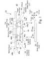
- FIG. 1is a detailed schematic diagram of a probe card assembly
- FIG. 2is a detailed schematic view of a contactor assembly comprising an array of compliant micro-fabricated spring contacts
- FIG. 3is a detailed partial cross sectional view of an interposer structure
- FIG. 4shows a soldered contactor probe card embodiment having a double-sided upper interposer
- FIG. 5shows a soldered contactor probe card embodiment having a soldered upper interposer
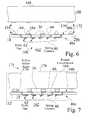
- FIG. 6is a first schematic view of solder ball re-flow contactor construction
- FIG. 7is a second schematic view of solder ball re-flow contactor construction
- FIG. 8is a first schematic assembly view of a high-density connector having fan-out
- FIG. 9is a second schematic assembly view of a high-density connector having fan-out
- FIG. 10is a detailed schematic view of a first exemplary embodiment of assembly latch construction
- FIG. 11is a detailed schematic view of a second exemplary embodiment of assembly latch construction
- FIG. 12is a detailed schematic view of a third exemplary embodiment of assembly latch construction
- FIG. 13is a detailed schematic view of a fourth exemplary embodiment of assembly latch construction
- FIG. 14is a first schematic assembly view of a high density BGA socket connector embodiment
- FIG. 15is a second schematic assembly view of a high density BGA socket connector embodiment
- FIG. 16is a detailed partial sectional view of a centered-contact micro-fabricated spring contact connection for an exemplary high-density connector
- FIG. 17is a detailed partial sectional view of a leading-edge micro-fabricated spring contact connection for an exemplary high-density connector
- FIG. 18is a detailed partial sectional view of an over-center micro-fabricated spring contact connection for an exemplary high-density connector
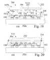
- FIG. 19is a first schematic assembly view of a BGA lattice-socket connector embodiment
- FIG. 20is a second schematic assembly view of a high density BGA lattice-socket connector embodiment
- FIG. 21is a plan view of a first embodiment of a high density BGA lattice-socket connector embodiment
- FIG. 22is a plan view of a second embodiment of a high density BGA lattice-socket connector embodiment
- FIG. 23is a first schematic assembly view of a high-density low profile board-to-board contactor
- FIG. 24is a second schematic assembly view of a high-density low profile board-to-board contactor
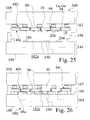
- FIG. 25is a first schematic assembly view of a high-density low profile board-to-board contactor with fan-out;
- FIG. 26is a second schematic assembly view of a high-density low profile board-to-board contactor with fan-out;
- FIG. 27is a first schematic assembly view of a solderless chip mount embodiment
- FIG. 28is a second schematic assembly view of a solderless chip mount embodiment
- FIG. 29is a first schematic assembly view of a system in package (SIP) embodiment
- FIG. 30is a second schematic assembly view of a system in package (SIP) embodiment
- FIG. 31is a schematic assembly view of Z-compliant connector construction for an exemplary article of manufacture
- FIG. 32shows a first exemplary embodiment of board to board connector construction
- FIG. 33shows a second exemplary embodiment of a board to board connector construction
- FIG. 34is a first schematic plan view of a contactor having asymmetric connections
- FIG. 35is a second schematic plan view of a contactor having asymmetric connection arrays
- FIG. 36is a schematic partial cutaway view of a connector having asymmetric axial connectivity in a first position
- FIG. 37is a schematic partial cutaway view of a connector having asymmetric axial connectivity in a second position
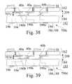
- FIG. 38is a schematic partial cutaway view of a connector having asymmetric axial connectivity in a third position.
- FIG. 39is a schematic partial cutaway view of a connector having asymmetric axial connectivity in a fourth position.
- PCT/US00/14164entitled Construction Structures and Manufacturing Processes for Integrated Circuit Wafer Probe Card Assemblies, US Filing Date 23 May 2000; and U.S. patent application Ser. No. 10/069,902, entitled Systems for Testing and Packaging Integrated Circuits, filed 28 Jun. 2002, each of which are incorporated herein in its entirety by this reference thereto.
- Micro-fabricated spring contactsmay be fabricated with variety of processes known to those skilled in the art.
- Exemplary monolithic micro-fabricated spring contactsmay comprise stress metal springs which are photolithographically patterned and fabricated on a substrate using batch mode semiconductor manufacturing processes.
- the spring contactsare fabricated en masse, and can be fabricated with spacings equal to or less than that of semiconductor bonding pads or with spacings equal to or greater than those of printed circuit boards, i.e. functioning as an electrical signal space transformer.
- Monolithic micro-fabricated spring contacts 40such as seen in FIG. 2 , comprise a unitary, i.e. integral construction or initially fabricated using planar semiconductor processing methods, whereas non-monolithic spring contacts are typically assembled from separate pieces, elements, or components.
- Non-monolithic or monolithic micro-fabricated spring contactscan be fabricated on one or both sides of rigid or flexible contactor substrates having electrically conductive through-vias and multiple electrical signal routing layers on each side of the substrate to provide electrically conductive paths for electrical signals running from spring contacts on one side of the substrate to spring contacts or other forms of electrical connection points on the opposite side of the substrate through signal routing layers on each side of the substrate and one or more electrically conductive vias fabricated through the substrate.
- optical signalscan be transmitted through the contactor substrate by fabricating openings of sufficient size through the substrate through which the optical signals can be transmitted.
- the holesmay be unfilled or filled with optically conducting materials including but not limited to polymers, glasses, air, vacuum, etc.
- Lenses, diffraction gratings and other optical elementscan be integrated to improve the coupling efficiency or provide frequency discrimination when desired.
- An exemplary monolithic micro-fabricated spring contact comprising a stress metal springis fabricated by sputter depositing a titanium adhesion/release layer having a thickness of 1,000 to 5,000 angstrom on a ceramic or silicon substrate (approximately 10-40 mils thick) having 1-10 mil diameter electrically conductive vias pre-fabricated in the substrate. Electrically conductive traces fabricated with conventional photolithographic processes connect the spring contacts to the conductive vias and to the circuits to which they ultimately connect.
- a common material used to fabricate stress metal springsis MoCr, however other metals with similar characteristics, e.g. elements or alloys, may be used.
- An exemplary stress metal spring contactis formed by depositing a MoCr film in the range of 1-5 ⁇ m thick with a built-in internal stress gradient of about 1-5 GPa/ ⁇ m.
- An exemplary MoCr filmis fabricated by depositing 2-10 layers of MoCr, each layer about 0.2-1.0 ⁇ m thick. Each layer is deposited with varying levels of internal stress ranging from up to 1.5 GPa compressive to up to 2 GPa tensile.
- Individual micro-fabricated stress metal spring contact “fingers”are photolithographically patterned and released from the substrate, using an etchant to dissolve the release layer.
- the sheet resistance of the fingercan be reduced by electroplating with a conductive metal layer (such as copper or gold).
- the force generated by the spring contactcan be increased by electrodepositing a layer of a material, such as nickel, on the finger to increase the spring constant of the finger.
- the quality of the electrical contactcan be improved by electrodepositing depositing a material, such as Rhodium 104 , onto the tip 86 through a photomask, prior to releasing the finger from the substrate.
- the lift height of the spring contactsis a function of the thickness and length of the spring and the magnitude of the stress gradient within the spring.
- the lift heightis secondarily a function of the stress anisotropy and the width of the spring and the crystal structure and stress in the underlying stress metal film release layer.
- the spring constant of the springis a function of the Young's Modulus of the material used to fabricate the spring and the length, width, and thickness of the spring.
- the spring constant of the springcan be increased by enveloping the springs 40 with a coating of a metal including but not limited to electroplated, or sputtered, or CVD deposited nickel or a nickel alloy, gold, or a palladium alloy such as palladium cobalt (see FIG. 1 ).
- the spring constantcan be varied over many orders of magnitude by controlling the thickness of the deposited coating layer, the geometrical characteristics of the spring, and the choice of metal and the thickness and number of coatings. Making the springs thicker both increases the contact force and the robustness of the physical and electrical contact between the spring and its contact pad.
- FIG. 1is a detailed schematic diagram 10 of a probe card assembly 42 .
- the probe card assembly 42comprises a probe card interface assembly (PCIA) 41 and a contactor assembly 18 , wherein the probe card interface assembly (PCIA) 41 comprises a motherboard 12 having electrical connections 132 ( FIG. 4 ) extending there through, and an integrated contactor mounting system 14 .
- Electrical trace paths 32extend through the motherboard 12 , the contactor mounting system 14 , and the contactor assembly 18 , to spring contacts, i.e. spring probes 40 , such as to establish contacts with pads 28 on one or more ICs 26 on a semiconductor wafer 20 .
- Fan-out 34may preferably be provided at any point for the electrical trace paths 32 in a probe card assembly 42 (or in other embodiments of the systems disclosed herein), such as to provide transitions between small pitch components or elements, e.g. contactors 18 , and large pitch components or elements, e.g. tester contact pads 126 ( FIG. 4 ) on the mother board 12 .
- fan-outmay typically be provided by the mother board 12 , the contactor 30 , by a Z-block 16 , by an upper interface 24 comprising a motherboard Z-Block, or anywhere within the lower interface 22 and/or the upper interface 24 .
- the contactor mounting system 14typically comprises a Z-block 16 , a lower interface 22 between the Z-block 16 and the contactor substrate 30 , and an upper interface 24 between the Z-block 16 and the motherboard 12 .
- the lower interface 22comprises a plurality of solder bonds 112 ( FIG. 4 ).
- the upper interface 24comprises a combination of componentry and connections, such as an interposer 122 , e.g. 122 a ( FIG. 8 ) or 122 b ( FIG. 5 ), solder bonds and/or a motherboard Z-block.
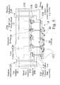
- FIG. 2is a detailed schematic view 60 of a contactor assembly 18 , in which the non-planar portions of compliant spring probes 40 are preferably planarized and/or plated.
- a contactor 18comprises a contactor substrate 30 having a probing surface 48 a and a bonding surface 48 b opposite the probing surface 48 a , a plurality of spring probes 40 on the probing surface 48 a , typically arranged to correspond to the bonding pads 28 ( FIG.
- contacts 40are described herein as spring contacts 40 , for purposes of clarity, the contacts 40 may alternately be described as contact springs, spring probes or probe springs.
- Non-monolithic micro-fabricated spring contacts 40utilize one or more mechanical (or micro-mechanical) assembly operations
- monolithic micro-fabricated spring contactsexclusively utilize batch mode processing techniques including but not limited to photolithographic processes such as those commonly used to fabricate MEMs devices and semiconductor integrated circuits.
- the electrically conductive monolithically formed contacts 40are formed in place on the contactor substrate 30 .
- the electrically conductive monolithically formed contacts 40are formed on a sacrificial or temporary substrate 63 , and thereafter are removed from the sacrificial or temporary substrate 63 , e.g. such as by etchably removing the sacrificial substrate 63 , or by detaching from a reusable or disposable temporary substrate 63 , and thereafter affixing to the contactor substrate 30 .
- Both non-monolithic and monolithic micro-fabricated spring contactscan be utilized in a number of applications including but not limited to semiconductor wafer probe cards, electrical contactors and connectors, sockets, and IC device packages.
- Sacrificial or temporary substrates 63may be used for spring fabrication, using either monolithic or non-monolithic processing methods.
- Spring contacts 40can be removed from the sacrificial or temporary substrate 63 after fabrication, and used in either free standing applications or in combination with other structures, e.g. contactor substrate 30 .
- a plane 72 of optimum probe tip planarityis determined for a contactor 18 as fabricated.
- Non-planar portions of spring contacts 40 located on the substrate 30are preferably plated 60 , and are then planarized, such as by confining the probes 40 within a plane within a fixture, and heat treating the assembly.
- the non-planar portions of the spring probes 40may also be plated after planarization, to form an outer plating layer 70 .
- the contactor assembly 18 shown in FIG. 2further comprises fan-out 34 , such as probe surface fan-out 34 a on the probe surface 48 a of the contactor substrate 18 and/or rear surface fan-out 34 b on the bonding surface 48 b of the contactor substrate 18 .
- fan-out 34such as probe surface fan-out 34 a on the probe surface 48 a of the contactor substrate 18 and/or rear surface fan-out 34 b on the bonding surface 48 b of the contactor substrate 18 .
- FIG. 3is a partial cross sectional view 78 of an interposer structure 80 , such as for a dual-sided interposer 80 a , Similar construction details are preferably provided for a single-sided interposer 80 b ( FIG. 5 ).
- Interposer springs 86are generally arranged within an interposer grid array, to provide a plurality of standardized connections.
- the interposer springs 86provide connections between a motherboard 12 and a Z-block 16 .
- the interposer springs 86provide connections between a motherboard 12 and an interposer 80 b.
- Interposer vias 84extend through the interposer substrate 82 , from the first surface 102 a to the second surface 102 b .
- the interposer vias 84may preferably be arranged in redundant via pairs, such as to increase the manufacturing yield of the interposer 80 , and/or to promote electrical conduction, particularly for power traces.
- the opposing surfaces 102 a , 102 bare typically comprised of a release layer 90 , such as comprising titanium, and a composite layer 88 , 92 , typically comprising a plurality of conductive layers 88 a - 88 n , having different inherent levels of stress.
- Interposer vias 84e.g. such as CuW or gold filled, extend through the central substrate 82 , typically ceramic, and provide an electrically conductive connection between the release layers 90 .
- the composite layers 88 , 92typically comprise MoCr (however other metals with similar characteristics, e.g. elements or alloys, may be used), in which the interposer probe springs 86 are patterned and subsequently to be later released within a release region 100 .
- a seed layer 94such as a 0.5 to 1 um thick gold layer, is preferably formed over the composite layers 88 , 92 .
- a tip coating 104such as rhodium or palladium alloy, is controllably formed at least over the tips of spring fingers 86 , such as to provide wear durability and/or contact reliability.
- Traces 96typically comprising copper, are selectably formed by plating over the structure 78 , as shown, such as to provide reduced resistance.
- polyimide PMID layers 98are typically formed over the structure 78 , as shown, to define the spring finger lift regions.
- a seed layer 94such as comprising a thick layer of gold, remains on the lifted fingers 86 , so as to reduce sheet resistance of the fingers 86 .
- FIG. 4is a detailed partial schematic view 110 of a probe card assembly system 42 a comprising a soldered contactor probe card 18 having a double-sided upper interposer 80 a .
- FIG. 5is a detailed partial schematic view 150 of a probe card assembly system 42 b comprising a soldered contactor probe card embodiment having a single sided upper interposer 80 b .
- One or more travel stops 152can preferably be included on an interface having compliant interposer spring probes 136 , e.g. stress metal spring probes 86 ( FIG. 3 ), to prevent the probes 136 from damage, such as if the upper interposer 80 b in FIG. 5 is bottomed out against the probe card motherboard 12 .
- the upper interposer 80 bmay be plated to increase the probe force of interposer spring probes 136 .
- Outer alignment pins 130typically extend from the top stiffener 38 through the probe card assembly 42 , such as through the probe card interface assembly 41 .
- the outer alignment pins 130engage mechanical registration features 134 , such as notches, slots, and/or holes, or any combination thereof, defined in components in the probe card assembly 42 , such as the motherboard 12 and the Z-block flange 144 .
- the use of registration features 134preferably allows for differences in thermal expansion between components in the probe card assembly 42 , to allow testing over a wide temperature range.
- FIG. 6is a first schematic view 160 of solder ball re-flow contactor construction 162 .
- FIG. 7is a second schematic view 174 of solder ball re-flow contactor construction 162 .
- a contactor assembly 18having reflowed solder ball connections 112 to a second structure 166 , such as substrate 168 , e.g.
- solder balls 164are located on electrically conductive pads 64 on the rear bonding surface 48 b of a probe spring substrate 30 , which are configured to be aligned with electrically conductive contact pads 170 , e.g. gold or solder coated, etc. located on a mating structure 166 , such as substrate 168 , such as comprising any of ceramic, multi-layer ceramic, glass ceramic, glass, quartz, glass epoxy, FR-4, polyimide, a semiconductor wafer, silicon, a printed circuit board, one or more flip chip semiconductor devices, one or more packaged semiconductor devices, a semiconductor integrated circuit, and a hybrid integrated circuit.
- the probe spring assembly 18 and the mating structure 166are then movably positioned together 172 , such as within an appropriate fixture 178 . As seen in FIG. 7 , heat is then applied to the assembly 162 , such that the solder balls 164 reflow 176 to form probe assembly solder joints 112 ( FIG. 4 , FIG. 5 ).
- the established planarity of the contactor assembly 162 by the bonded solder joints 112provides an assembly which can advantageously be used throughout a wide variety of advanced interconnection structures, such as but not limited to:
- probe card assembliesfor probing wafer level packages, flip chip devices, chip scale packages, under bump metal, solder, solder balls, displays, display drivers, area arrays, etc.;
- miniaturized or high density connector assembliese.g. such as for consumer electronic products, cell phones, PDAs, cameras, projectors, imaging devices, etc.;
- socket assembliese.g. high density, low insertion force, solder ball array, land grid array (LGA), etc.;
- silicon substratescan be used to provide TCE match between the contactor and the device under test
- WLPwafer level packages
- singulated diee.g. singulated die
- multi-die packagese.g. system in a package (SiP) including embodiments with non-uniform die thicknesses, and/or three dimensional packages, e.g. stacked die.
- SiPsystem in a package
- three dimensional packagese.g. stacked die.
- FIG. 8is a first schematic assembly view of a high-density connector 182 a having fan-out 34 .
- FIG. 9is a second schematic assembly view of a high-density connector 182 a having fan-out 34 .
- a contactor assembly 18provides high-density connections 214 between a contactor structure 162 and a secondary connector structure 184 .
- the exemplary connector structure 184 shown in FIG. 8 and FIG. 9comprises one or more substrates 186 , 188 having electrically conductive paths 194 defined therethorugh, typically having a first set of electrically conductive pads 190 which correspond to spring probe contacts 40 on the spring probe assembly 18 , and a second set of electrically conductive pads 196 opposite the connector structure 184 from the first set of electrically conductive pads 190 .
- the second set of electrically conductive pads 196correspond to connectors or contacts from an external structure, such as a printed circuit board or a cable connector.
- the connector structure 184comprises a connector body 186 , 188 having multi-layer thin film circuitry and electrically conductive through-vias 194 .
- a contactor assembly 18comprises a top connector element within a contactor structure 162 , such as seen in FIG. 6 and FIG. 7 .
- the probe card assembly 18 seen in FIG. 8 and FIG. 9preferably comprises fan-out 34 , such as 34 a , 34 b ( FIG. 2 ).
- Conductive bonds 112are located between the contactor assembly 118 and the second structure 166 , which preferably comprise solder joints 112 .
- the high-density connector 182 a seen in FIG. 8 and FIG. 9comprises means for connection 214 between the contactor structure 162 and the secondary connector structure 184 , wherein establish connections 214 are established between the spring probes 40 and the first set of electrically conductive pads 190 .
- the means for connection 214preferably comprises one or more latches 212 between the contactor structure 162 and the secondary connector structure 184 , such that the contactor structure 162 and the secondary connector structure 184 are movable 208 with respect to one another ( FIG. 8 ), and also provide means for fixedly attaching, i.e. latching, when the contactor structure 162 and the secondary connector structure 184 are controllably positioned together.
- the latches 212may provide unlatching, such as for service or for replacement of assemblies. In other applications, the latches 212 may be considered to be single-use latches, such as for but not limited to consumer electronics products.
- connection means 214may preferably comprise one or more latches 212 formed by a first latch element 200 located on the contactor structure 162 , which is matably connectable to a second latch structure 202 located on the secondary connector structure 184 .
- the connection means 214 seen in FIG. 8 and FIG. 9also preferably comprises means for alignment 198 between the contactor structure 162 and the secondary connector structure 184 , such as one or more mechanical alignment guides 198 , which may be affixed at a variety of locations in various embodiments of the connectors 182 , such as to the contactor structure 162 , e.g. directly to the contactor assembly 18 , or alternately directly to the second structure 166 ( FIG. 23,24 ), or to the secondary connector structure 184 ( FIG. 21 , FIG. 22 ).
- High-density connectors 182may also comprise one or more travel stops 204 , 206 , such as to establish and/or protect the spring probes 40 and/or the electrical connections 214 between the spring probes 40 and the first set of electrically conductive pads 190 .
- a first set of travel stops 204acts as means to dampen the latch connections 212 , such as to dampen vibration or movement in the assembly 182 , i.e. to absorb shock.
- the second set of travel stops 206prevents damage to the spring probes 40 during assembly, use, and/or service.
- connection means 214can be provided within various embodiments of high-density connectors 182 , for latching 212 and/or alignment between contactor structures 162 and secondary connector structures 184 .
- FIG. 10is a detailed schematic view 214 of a first exemplary embodiment of assembly latch construction 212 a .
- a portion of a contactor structure 162such as a contactor assembly substrate 30 , may be fixedly connected or otherwise attached to one or more alignment guides 198 , which may typically include a first latch element 218 a , e.g. a detent or keep, either integrally or associated with a latch element 216 .
- a portion of a secondary structure 184such as a substrate 186 , may typically include a second latch element 218 b , e.g. a keep or detent.
- the contactor structures 162 and secondary connector structures 184are movable 208 in relation to each other, e.g. linearly movable on Z-axis 27 ( FIG. 1 ), to establish a mating latch connection 212 a between the latch elements 218 a and 218 b.
- FIG. 11is a detailed schematic view 220 of a second exemplary embodiment of assembly latch construction 212 b .
- a portion of a contactor structure 162such as a contactor assembly substrate 30 , may be fixedly connected or otherwise attached to one or more alignment guides 198 , which may typically include a detent keep assembly, such as comprising a detent 226 , a spring 222 , and attachment means 224 .
- a portion of a secondary structure 184such as the substrate 186 , may typically include a second latch element 218 b , e.g. a detent, keep, hole, or groove, to attach to the first latch element 218 a .
- a second latch element 218 be.g. a detent, keep, hole, or groove
- the alignment guides 198may preferably include a ledge detail 228 which can act as a travel stop, such as in combination with a lower surface 187 a of the substrate 186 , for latching 212 and/or alignment between contactor structures 162 and secondary connector structures 184 .
- FIG. 12is a detailed schematic view 230 of a third exemplary embodiment of assembly latch construction 212 c .
- One or more alignment guides 198may alternately include first latch element 218 a comprising one or more spring latches 232 , fasteners 234 , and one or more travel stops 204 .
- a portion of a secondary structure 184such as the rear surface 187 b of the substrate 186 , acts as a second latch element 218 b .
- the spring latches 232catch and fixedly retain the rear surface 187 b of the substrate 186 .
- FIG. 13is a detailed schematic view 240 of a fourth exemplary embodiment of assembly latch construction 212 d .
- a portion of secondary structure 184such as substrate 188 , 186 , may be fixedly connected or otherwise attached to one or more alignment guides 198 , which may typically include a first latch element 218 a , e.g. a detent or keep, either integrally or associated with a latch element 216 ( FIG. 10 ).
- a portion of a contactor structure 162such as the substrate 168 or the contactor substrate 30 , may typically include a second latch element 218 b , e.g. a keep or detent.
- the contactor structures 162 and secondary connector structures 184are movable 208 in relation to each other, e.g. linearly movable on Z-axis 27 ( FIG. 1 ), to establish a mating latch connection 212 d between the latch elements 218 a and 218 b.
- FIG. 14is a first schematic assembly view 250 of a high-density connector 182 b , in which the secondary connector structure 184 comprises a high density socketed package 252 .
- Package 252may be a ball grid array (BGA), a land grid array (LGA) or other device package having a substrate 186 .
- Electrically conductive pads 190optionally comprise a surface coating layer (e.g., gold, solder, etc.).
- Substrate 186may comprise ceramic, glass ceramic, glass, glass epoxy, FR-4, polyimide, silicon, a printed circuit board, or a flip chip semiconductor device.
- FIG. 15is a second schematic assembly view 264 of a high-density connector 182 b , in which the secondary connector structure 184 comprises a high density socketed package 252 .
- An array 254 of solder balls 255are optionally located on the lower surface of the electrically conductive pads 190 , which are located directly on the lower surface 187 a adjacent to electrical connection terminals 191 .
- the high-density connector 182 bcan be used to serve a wide variety of functions such as an intermediate connection 259 , in conjunction with one or more components 258 , e.g. 258 a - 258 j , within the package 252 , and/or in conjunction with one or more heat sinks 256 , e.g. 256 a - 256 k , which may preferably include thermal paste junctions 257 to facilitate heat transfer.
- the components 258 a - 258 jmay comprise a variety of active and/or passive elements.
- the heat sinksmay be used for heat transfer associated with one or more of the components 258 a - 258 j and the contactor structure 162 .
- connection means 214may preferably comprise one or more matably connectable latches 212 established between the contactor structure 162 and the secondary connector structure 184 .
- the connection means 214 seen in FIG. 14 and FIG. 15may also preferably comprise means for alignment 198 between the contactor structure 162 and the secondary connector structure 184 , such as one or more mechanical alignment guides 198 , which may be affixed at a variety of locations in the high-density connector 182 b , such as to the contactor structure 162 , e.g. directly to the contactor assembly 18 , or alternately directly to the second structure 166 ( FIG. 23,24 ), or to the secondary connector structure 184 ( FIG. 21 , FIG. 22 ).
- FIG. 16is a detailed partial sectional view of a centered-contact spring connection 270 a for an exemplary high density connector 182 .
- FIG. 17is a detailed partial sectional view of a leading-edge contact spring connection 270 b for an exemplary high density connector 182 .
- FIG. 18is a detailed partial sectional view of an over-center contact 270 b spring connection for an exemplary high density connector 182 .
- a compliant spring 40extending from a first connector structure 162 , such as from a contactor substrate 30 , makes an electrical connection 272 with a correspondingly opposing electrically conductive pad 190 extending from a second connector structure 184 , such as from a substrate 186 .
- an electrically conductive solder ball 255is located on the electrically conductive pad 190 , and defines a convex surface having a relatively horizontal center 272 .
- the first connector structure 162 and the second connector structure 184are associatively positioned 274 such that the tip 62 of the compliant spring 272 is aligned with the center 272 of electrically conductive solder ball 255 .
- the first connector structure 162 and the second connector structure 184are associatively positioned 274 such that the tip 62 of the compliant spring 40 is offset 276 from the center 272 of electrically conductive solder ball 255 , such that the tip 62 connects to the electrically conductive solder ball 255 on a leading, i.e. face surface 277 .
- the first connector structure 162 and the second connector structure 184are associatively positioned 274 such that the tip 62 of the compliant spring 40 is offset 276 from the center 272 of electrically conductive solder ball 255 , such that the tip 62 connects to the electrically conductive solder ball 255 on a trailing, i.e. back surface 279 .
- embodiments of the high density interconnectorscan preferably provide a wide variety of electrical connections between the first connector structure 162 and the second connector structure 184 , such as to prevent damage to solder balls 255 and/or compliant springs 40 .
- one or more established connections between a first connector structure 162 and a second connector structure 184may deform the center of one or more solder balls 255 , whereby solder reflow may be desired to service the second connector structure 184 .
- some preferred high density interconnectors 182may alternately provide leading-edge contact spring connections 270 b and/or over-center contact spring connections 270 b , such as to provide a high quality connection over repeated usage.
- some preferred high density interconnectors 182provide controlled offset of an array of springs 40 associated with an array of solder balls 255 , e.g. having tips 62 on opposite sides of adjacent solder balls 255 , such as to balance connection forces across a connector, i.e. to promote self centering and prevent a skewed connection between the first connector structure 162 and the second connector structure 184 .
- spring contacts 40 on the contactor substrate 30that approximately balance the lateral forces on the solder balls 255 generated by the spring contact tips 62 across the connector 182 .
- one spring contact 40may be provided for each solder ball 255 .
- Lateral forces across the connector 182can be minimized and approximately balanced by providing approximately equal numbers of spring contacts 40 on opposite sides of the solder balls 255 , e.g. the leading and trailing edges of every other solder ball 255 .
- at least some of the spring contacts 40may be located to offset respective lateral forces applied to associated solder balls 255 , and/or the resulting forces applied to the spring contacts 40 .
- FIG. 19is a first schematic assembly view 280 of a high-density connector 182 c , in which the secondary connector structure 184 comprises a high density socketed package 252 , and in which the contactor assembly 18 comprises a plurality of spring contacts 40 corresponding to each solder ball connection 255 in a ball grid array 254 .
- Package 252may be a ball grid array (BGA), a land grid array (LGA) or other device package having a substrate 186 . In cases where optional solder balls 255 are not present, e.g. package 252 is a LGA, spring contacts 40 will directly contact the electrically conductive pads 190 .
- the substrate 186may comprise ceramic, glass ceramic, glass, glass epoxy, FR-4, polyimide, silicon, a printed circuit board, a semiconductor device package, or a flip chip semiconductor device.
- FIG. 20is a second schematic assembly view 310 of a high-density connector 182 c .
- the high-density connector 182 cmay be configured and function in a similar manner to the high-density connector 182 b .
- the preferable inclusion of a plurality of spring contacts 40e.g. 40 a - 40 d can be used for any of reliability, redundancy, applications which require increased current or voltage requirements, and mechanical robustness, i.e. providing robust and force balanced connections to optional electrically conductive pads 190 , solder balls 255 , and/or ball grid array 254 .
- FIG. 21is a partial plan view of a first embodiment 316 a of a high density spring contact lattice-socket connector 182 c .
- FIG. 22is a partial plan view of a second embodiment 316 b of a high density spring contact lattice-socket connector 182 c.
- each probe spring set 322 acomprises a plurality of spring probes 40 , e.g. 40 a - 40 d , in which the probe spring sets 322 a are aligned in an array of one or more rows 324 and columns 326 , to correspond to solder balls 255 located on a lower surface 187 a of a second connector structure 184 .
- Spring probe sets 322may comprise any convenient number of spring probes, such as but not limited to 1, 2, 3 and/or 4 springs 40 .
- spring probes 40are also axially aligned 321 , 323 to the rows 324 and columns 326 respectively, which can limit the density of the connector 182 c and/or the length of the compliant springs 40 .
- each probe spring set 322 balso comprises a plurality of spring contacts 40 , e.g. 40 a - 40 d , in which the spring contact sets 322 b are aligned in an array of one or more rows 324 and columns 326 , to correspond to solder balls 255 or electrically conductive pads 190 located on a lower surface 187 a of a second connector structure 184 .
- spring contacts 40are also diagonally skewed, e.g. rotated 327 with respect to the rows 324 and/or columns 326 , which provides an increase in connection density for the connector 182 c and/or provides an increased length for the compliant spring contacts 40 .
- FIG. 23is a first schematic assembly view 330 of a high-density low profile substrate-to-substrate connector 182 d .
- FIG. 24is a second schematic assembly view 350 of a high density low profile substrate-to-substrate connector 182 d .
- a lower substrate 166 and an upper substrate 188are latchably connected 212 , such as between standoffs 332 extending from the secondary connector structure 184 , e.g. such as affixed to or through the upper substrate 188 , and alignment guides 198 extending from the contactor structure 162 , e.g. such as affixed to either the contactor assembly 18 or to the lower substrate structure 166 .
- the lower and upper substrates 166 and 168may comprise any of ceramic, multi-layer ceramic, glass ceramic, glass, quartz, glass epoxy, FR-4, polyimide, a semiconductor wafer, silicon, a printed circuit board, one or more flip chip ICs, one or more packaged semiconductor devices, a semiconductor integrated circuit, and a hybrid integrated circuit.
- the standoffs 332may preferably be configure to function as travel stops for a latched assembly 182 , e.g. 182 d.
- FIG. 25is a first schematic assembly view 360 of a high density low profile substrate-to-substrate connector 182 e with fan-out 34 .
- FIG. 26is a second schematic assembly view 380 of a high density low profile substrate-to-substrate connector 182 e with fan-out 34 .
- High-density connectors 182inherently provide high-quality high density electrical connections within a latchable assembly, which can provide fan-out on either or both sides 162 , 184 of the latch region 212 .
- Lower and upper substrates 166 and 168may comprise ceramic, glass ceramic, glass, glass epoxy, FR-4, polyimide, silicon, a printed circuit board, one or more packaged ICs, or one or more flip chip ICs.
- High-density connectors 182also inherently provide a high degree of planarity within the latching region 212 , and also provide planarity compliance through the use of compliant, i.e. flexible spring probes 40 .
- TCEThermal Coefficient of Expansion
- high-density connectors 182inherently provides means for cost effective solutions to each of these problems.
- the X-Y compliance of the spring probes 40which preferably comprise micro-fabricated spring contacts, compensates for TCE mismatch between a device and a printed circuit board, while the Z-compliance of the spring probes 40 compensates for lack of co planarity.
- Z-compliance and customizable length springsaccommodates chips with different substrate thickness, such as for multiple-die packages, e.g. system in package (SiP).
- SiPsystem in package
- multilevel metalcan be used to provide controlled impedance and shielded signal paths.
- preferred embodiments of high-density connectors 182which utilize photolithographic self-assembling springs have an advantageous cost/performance ratio.
- FIG. 27is a first schematic assembly view 400 of a high-density connector 182 f for the solderless mounting of one or more contactor assemblies 18 , such as for a contactor assembly that comprises a chip scale package.
- FIG. 28is a second schematic assembly view 420 of a high-density connector 182 f for the solderless mounting of one or more contactor assemblies 18 .
- a lower structure 162 bcomprises a contactor scale package 18 b located on a structural element 402 , such as a planar heat sink, carrier, or surface mount package substrate 402 .
- a secondary structure 184includes a substrate 188 comprising any of ceramic, multi-layer ceramic, glass ceramic, glass, quartz, glass epoxy, FR-4, polyimide, silicon, and a printed circuit board.
- the secondary structure 184also comprises electrically conductive pads 190 on the lower surface 187 a .
- Meansare provided for positioning 198 the lower structure 162 b and secondary structure 184 in relation to each other, whereby their position may be aligned by one or more travel guides 198 .
- the secondary structure 184is also latchably attachable 212 to the lower structure 162 b , such as by corresponding latch elements 218 a , 218 b.
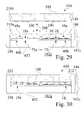
- FIG. 29is a first schematic assembly view 430 of a high-density connector 182 f for a system in package (SIP) embodiment.
- FIG. 30is a second schematic assembly view 450 of a high-density connector 182 f for a system in package (SIP) embodiment.
- a lower structure 162 ccomprises one ore more contactor scale packages 18 , e.g. 18 a - 18 j , located on a structural element 432 , such as a planar heat sink, carrier, or surface mount package substrate 432 .
- a secondary structure 184such as comprising ceramic, glass ceramic, glass, glass epoxy, FR-4, polyimide, silicon, a printed circuit board 188 , one or more packaged ICs, or one or more flip chip ICs, having electrically conductive contact pads 190 , accommodates relative movement in relation to the lower structure 162 c , whereby the movement 208 may be aligned by one or more travel guides 198 .
- the secondary structure 184is also latchably attachable 212 to the lower structure 162 c , such as by corresponding latch elements 218 a , 218 b.
- contactor scale packages 18 a - 18 jcomprise integrated circuit packages which may have the same or differing substrate thicknesses 75 a - 75 j .
- integrated circuit packages 18 a - 18 jmay comprise non-monolithic or monolithic micro-fabricated spring contacts to provide compliant electrical connections circuit board 188 .
- the spring contact tips 62are positioned at a standard height from the supported rear surface 48 b of the integrated circuit devices 18 , i.e. adjusted to compensate for differences in thicknesses 75 of the integrated circuit device substrates 30 .
- the spring contact tips 62may are positioned at a fixed height from the contact surface 48 a of the integrated circuit device substrates 30 , i.e. the compliance of the spring contacts 40 provide compensation for differences in thicknesses of the integrated circuit device substrates 30 .
- FIG. 31is a schematic assembly view 460 of Z-compliant connector construction for an exemplary article of manufacture 462 , such as for but not limited to a camera, a video camera, a personal digital assistant (PDA), a solid state music player, e.g. an MP3 or an enhanced iPod, or for a multi-function device.
- PDApersonal digital assistant
- solid state music playere.g. an MP3 or an enhanced iPod
- a MEMS Z-Actuator 472having probe springs 40 , is slidably movable 463 on one or more actuator stators 468 .
- An image sensor, e.g. CCD, chip 474is mounted, e.g. surface mounted, to the opposing side of the MEMS Z-Actuator 472 .
- the actuator stators 468are affixed with respect to a printed circuit board 466 .
- the printed circuit board 466is affixed with respect to at the case structure 464 of the article 462 .
- a lens 478is typically located such that light 484 associated with a captured image 481 is controllably captured, i.e.
- An auto focus light source 480 and light detector 482may also be included, such that emitted light 486 is reflected and sensed as an input to a control 490 .
- the MEMS Z-Actuator 472is slidably movable 463 in the Z-direction 27 ( FIG. 1 ) on the actuator stators 468 , such as to any reference plane between and including a first position 465 a and a second position 465 b , wherein compliant contactor array 470 , comprising spring contacts 40 can preferably provide compliant electrical contacts to the printed circuit board 466 throughout the range of motion 465 a , 465 b.
- the effective focal plane 467 from the lens 478 to the image sensor 474is therefore controllably variable at any point between and including the first position 465 a and the second position 465 b .
- emitted light 486 from the auto focus light source 480is reflected off a subject SBJ and sensed by the light detector 482 , which acts as an input for control 490 .
- the controller 490moves the MEMS actuator 472 at any point between and including a first position 465 a and a second position 465 b , to provide a desired focal length 467 .
- An image 481is then typically controllably captured, such as by controlled opening of a shutter 483 , and stored to a memory 492 , which can then be downloaded or otherwise transferred, e.g. such as by a removable memory element 494 .
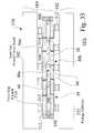
- FIG. 32is a detailed schematic view 500 of first exemplary board to board high-density connector 182 i , such as to provide any of a releasable or permanent connection between a high cost printed wiring board 168 and a low cost printed wiring board 502 .
- FIG. 33is a detailed schematic view 550 of secondary exemplary board to board high-density connector 182 j , such as to provide any of a releasable connection or permanent connection between a package substrate 552 and a low cost printed wiring board 502 .
- the exemplary secondary connector assembly 184 seen in FIG. 32 and FIG. 33comprises electrical connections 506 , such as but not limited to solder ball connections 506 , e.g. such as provided by reflow 176 , between a printed circuit board 502 and a lower connector substrate 504 .
- the lower connector substrate 504further comprises contact pads 512 on the upper surface, electrically conductive vias 508 extending through the lower connector substrate 504 , and lower contacts 190 , for connection with one or more corresponding probe springs 40 extending from the contactor assembly 18 .
- the exemplary latches 212 shown in FIG. 32 and FIG. 33comprise one or more alignment guides 198 , which latchably mate 218 a , 218 b , e.g. FIG. 10 - FIG. 13 , to one or more corresponding latches 516 , which may preferably further function as travel stops for the assembly.
- the assemblymay also preferably comprise dedicated travel stops 520 , such as extending from the lower connector substrate 504 .
- Some embodiments of the connector 182provide asymmetric connectivity, which is well suited for a large number of applications, such as but not limited to accessing alternate pathways, connection to different circuits and/or devices, and/or providing alternate connection redundancy.
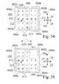
- FIG. 34is a first schematic plan view 600 a of a connector 182 having asymmetric connections.
- FIG. 35is a second schematic plan view 600 b of a connector 182 having asymmetric connection arrays.
- a first exemplary structure 162such as described above, comprises a plurality of sides 602 a , 602 b , 602 c and 602 d .
- the second exemplary structure 184such as described above, comprises a plurality of sides 606 a , 606 b , 606 c and 606 d .
- the first structure 162may also comprise an orientation detail 604
- the second structure 184may also comprise an orientation detail 608 .
- the first exemplary structure 162 seen in FIG. 34 and FIG. 35may comprise an asymmetric array 611 of first connective paths 612
- the second structure 184may comprise an asymmetric array of second connective paths 610 .
- an array 614 a of connections 214( FIG. 9 ) is defined for first connective paths 612 that coincide with second connective paths 610 .
- the first exemplary structure 162 and the second structure 184can be selectably oriented with respect to each other, e.g. by rotating the connectors 162 , 184 with respect to each other about the Z-axis 27 , i.e. in a plane defined by the X-axis 23 and the Y-axis 25 .
- the exemplary connector 182is oriented in a second position 600 b , wherein the first exemplary structure 162 and the second structure 184 are oriented such that side 602 a is aligned with 606 c
- an alternate array 614 b of connections 214is defined for first connective paths 612 that coincide with second connective paths 610 .
- the exemplary square connector 182 seen in FIG. 34 and FIG. 35may preferably include more than one asymmetric position, such as to rotate ninety degrees in any direction, e.g. wherein side 602 a is aligned second connector sides 606 b or 606 d , to provide alternate arrays 614 of connections 214 .
- exemplary connector 182 seen in FIG. 34 and FIG. 35is shown as a square connector 182 , e.g. comprising square symmetry between a first connector structure 162 and a second connector structure 184 , a wide variety of component shapes and geometric symmetries may be used, such as to provide asymmetric connections 214 , such as but not limited to symmetries based on rectangles, alternate polygons, and/or even cylinders with keyed, i.e. grooved mating details.
- some embodiments of the connector 182provide axial asymmetric connectivity which can also be adapted for a wide variety of applications, such as but not limited to accessing alternate pathways, connection to different circuits and/or devices, and/or providing alternate connection redundancy.
- axial movement 208can define an amount of insertion between a first connector structure 162 and a second connector structure 184 .
- Axial movement 208 in relation to an insertion axismay define any relative movement between a first connector structure 162 and a second connector structure 184 , such as between at least two positions, wherein positions may define positions of separation between springs 40 and opposing contacts 90 , position of first contact for one or more springs 40 , positions of compliant, i.e. compressed contact, and/or positions of contact limits, such as determined by one or more travel stops, latches, and/or detents.
- high-density interconnection assemblies 182provide springs 40 having relatively similar height 702 ( FIG. 36 ), and opposing pads 90 having relatively similar height 704 ( FIG. 36 ), such as to provide a plurality of connections between entire arrays of opposing springs 40 and electrically conductive pads 190 .
- alternate embodiments of high-density interconnection assemblies 182provide springs 40 having different heights 702 , and/or opposing electrically conductive pads 190 having different heights 704 , such as to provide differing arrays of connections between entire arrays of opposing springs 40 and electrically conductive pads 190 , based upon axial positioning relation to an insertion axis, e.g. Z-axis 27 .
- Spring height 702can be varied in a number of ways known to those skilled in the art, including, for example, by varying the design length of the springs on the substrate as defined by photolithography.
- Pad height 704can varied in a number of ways known to those skilled in the art, for example, by varying the thickness of metal plated onto the pad support substrate 186 , 188 .
- FIG. 36is a schematic partial cutaway view of a connector 182 having asymmetric axial connectivity in a first position 700 a .
- FIG. 37is a schematic partial cutaway view of a connector 182 having asymmetric axial connectivity in a second position 700 b .
- FIG. 38is a schematic partial cutaway view of a connector 182 having asymmetric axial connectivity in a third position 700 c .
- FIG. 39is a schematic partial cutaway view of a connector 182 having asymmetric axial connectivity in a fourth position 700 d.
- the first connector structure 162typically comprises a contactor substrate 30 having compliant springs 40 , e.g. 40 a , 40 b , extending away from the substrate 30 toward the second connector structure 184 .
- the compliant springs 40 shown in FIG. 36define a formed spring height 702 , such as relative either to the substrate 30 or to one of the layers, e.g. release layer 90 ( FIG. 3 ), upon which they are formed.
- the spring height 702 a for springs 40 ais less than the spring height 702 b for a spring 40 b.
- the second connector structure 184typically comprises a board substrate 186 , 188 having electrically conductive pads 90 extending away from the substrate 186 , 188 toward the first connector structure 162 .
- the pads 90 shown in FIG. 36define a pad height 704 , typically relative to the substrate 186 , 188 .
- pad height 704 a for pads 92 ais more than the pad height 704 b for a spring 92 b.
- the difference in heights 702 and 704inherently provides means for asymmetrical contacts with respect to an insertion axis, e.g. Z-axis 27 .
- an insertion axise.g. Z-axis 27 .
- the spring 40 bis electrically connected to an opposing 90 b
- springs 40 aare not electrically connected to corresponding pads 92 a , 92 b .
- FIG. 37As seen in FIG. 37 , at a position 700 b , wherein a first distance 707 a is defined between the contactor substrate 30 and the substrate 186 , 188 , the spring 40 b is electrically connected to an opposing 90 b , while springs 40 a are not electrically connected to corresponding pads 92 a , 92 b .
- the spring 40 bis partially compressed and is electrically connected to an opposing pad 90 b , while a second pad 90 b is electrically connected to an opposing spring 40 a , and while pad 92 b is not electrically connected to its corresponding pad 40 a .
- the spring 40 bis further compressed and is electrically connected to an opposing pad 90 b
- the second pad 90 bis electrically connected to an opposing compressed spring 40 a
- pad 92 bis electrically connected to its corresponding pad 40 a.
- the connectors 182 having asymmetric axial connectivity seen in FIGS. 36-39can therefore preferably provide one or more contactor states at different distances 707 , e.g. 707 a - 707 d , and can be used for a wide variety of applications, such as to connect one or more connected circuits based upon position 700 , and/or to provide sensing or control, such as to sense a limit for insertion travel 208 .
- High density connectors 182utilize arrays of micro-fabricated spring contacts 40 , fabricated on a substrate 18 , to provide simultaneous electrical contact between two objects, such as but not limited to components, devices, systems, sub-systems, and/or substrates.
- Some preferred embodiments of the connectors 182can be utilized for space confined applications, such as but not limited to cell phones, personal digital assistants (PDAs), computers, portable computers, medical devices, cameras, video cameras, printers, imaging devices, digital media players, and/or other portable electronic systems where it is desired to minimize the space required in the X, Y, or Z directions 23 , 25 , 27 or any combination thereof.
- the force versus displacement characteristics of the springs 40are controlled by the design of the spring 40 , and multiple types of spring characteristics can be provided in a single device, e.g. 18 , since the springs 40 are batch processed with photolithographic chip processing technologies. Force can be increased by adding plated metal layers, e.g. such as one or more layers ( 68 , 70 ( FIG. 2 ); 104 ( FIG. 3 )) or decreased by making the springs 40 longer, narrower, or thinner. Low force springs 40 can maintain electrical contact, while imparting minimal loading to external actuation systems.
- high density connectors 182comprise arrays of micro-fabricated spring contacts, fabricated on a substrate, to provide simultaneous electrical contact between two objects (including components, devices, systems, sub-systems, substrates, etc.) in applications where it is desired to maximize connection density or minimize the space required in the X, Y, or Z directions or any combination thereof and where it is desired to interconnect components with IC bond bad spacings to components with printed circuit board spacings.
- high density connectors 182comprise arrays of micro-fabricated spring contacts fabricated on multiple integrated circuit devices, to provide electrical contact between the integrated circuit devices and a common support substrate and thermal contact with a common heat sink wherein each device may have different thicknesses and/or coefficients of thermal expansion.
- high density connectors 182comprise arrays of micro-fabricated spring contacts 40 , fabricated on a substrate, e.g. contactor substrate 30 , at very high density to provide a small area, thin and inexpensive electrical connector between two objects (including components, devices, systems, sub-systems, and/or substrates).
- high density connectors 182comprise arrays of micro-fabricated spring contacts 40 , fabricated on one side of a flexible thin substrate, e.g. contactor substrate 30 , at very high density and the other side of the substrate 30 at a low density, so as to provide a space transforming function and thus to provide an inexpensive electrical connector between two objects, e.g. such as but not limited to components, devices, systems, sub-systems, and/or substrates, having widely varying electrical connection pitches.
- high density connectors 182comprise arrays of micro-fabricated spring contacts 40 , fabricated on a substrate 30 , to provide simultaneous electrical contact between two objects, e.g. such as but not limited to components, devices, systems, sub-systems, and/or substrates, over a range of distances between the objects and/or during relative motion of the objects with respect to each other.
- the tips 62 of the spring contacts 40can be soldered or otherwise affixed to the targeted electrical contact pads. Affixing the probe tips 62 to the electrically conductive pads 190 eliminates tip sliding and resists X, Y, and Z motion, however with an appropriate applied force, the position or orientation of one object with respect to the other can be changed and when the applied force is removed, the objects reposition themselves to the initial position assuming that all displacements have been small enough to avoid plastic deformation of the springs. With the tips of the spring contacts affixed to a support substrate, the spring contacts are capable of supplying both a pushing and a pulling force against external actuators.
- more than one spring contact designmay be employed to provide springs with differing characteristics to carry out differing functions.
- one type spring contactscan be designed and positioned to provide electrical contacts at specific locations whereas other types springs can be designed and positioned at other locations to provide mechanical forces to perform separate functions. This is possible since the mechanical characteristics of the springs can be changed by changing their length, width or their position yet since all of the springs are fabricated simultaneously, multiple types of springs can be provided with the same fabrication steps.
- substrateis intended to mean a thin or thick, inflexible or flexible, hard or soft insulating material that is chosen to be best suited for a particular application.
- Substratesare typically fabricated from single or multi-layer ceramic, glass ceramic, glass, quartz, semiconductors such as silicon, and/or polymers such as polyimide or printed circuit board materials, e.g. FR-4. Substrates may also be complete integrated circuits or hybrid integrated circuits. Substrates may be sacrificial or temporary wherein springs are fabricated, using either monolithic or non-monolithic processing methods, on a fabrication substrate. Springs can be removed from the fabrication substrate after fabrication and used in either free standing applications or in combination with other structures.
- TCEThermal Coefficient of Expansion
- the X-Y compliance provided by spring probes 40 in high-density connectors 182which preferably comprise micro-fabricated spring contacts 40 , compensates for TCE mismatch between a first connector assembly 162 and a second connector assembly 184 , such as between a device and a printed circuit board, while the Z-compliance of the spring probes 40 compensates for lack of co planarity.
- Z-compliance and customizable length springs 40accommodate chip packages 18 with different contactor scale package substrate thickness 75 , such as for multiple-die packages, e.g. system in package (SiP).
- multilevel metalcan be used to provide controlled impedance and shielded signal paths.
- preferred embodiments of high-density connectors 182 which utilize photolithographic self-assembling springshave an advantageous cost/performance ratio.
- first connector assembly 162 and a second connector assembly 184provide both a mechanical connection between the assemblies 162 , 184 , as well as a controlled connection environment, such as between the compliant spring probes 40 and opposing electrically conductive pads 190 .
- high-density connectors 182lowers the cost of ownership for many high-density assemblies, by allowing users to easily change contactor assemblies 18 and associated connector assemblies 162 , such as by disconnecting the latches 212 .
- the high-density connectors 182allow a trained user or field service engineer to quickly change either the first connector assembly, i.e. contactor 162 and/or a second connector assembly 184 , such as at a customer site.
- first connector assemblies 162 and/or second connector assemblies 184can keep an inventory of first connector assemblies 162 and/or second connector assemblies 184 on hand, and swap first connector assemblies 162 and/or second connector assemblies 184 as needed, instead of an entire high density electronic assembly. This capability minimizes downtime related to contactor issues, such as for regular scheduled cleaning, tip wear, tip failure, and/or unexpected tip contamination.
- High-density connectors 182comprise components with mechanical surfaces that are sufficiently flat and parallel to one another, that enable them to act as reference surfaces for other components either within the probe card assembly system, or that interface to the probe card assembly system. As well, the high density connectors 182 and associated processes maintain low resistance electrical connections to a device under test at either elevated or depressed operating temperatures.
- high-density connectors 182have relatively flat and parallel component surfaces, which more evenly distributes and vertically transmits the high forces associated with high I/O count connectors, to reduce peak-to peak mechanical deflections within the connector system, wherein the forces are generated either by the various spring pre-loading mechanisms or by the compression of the spring probes during connection.
- the high-density connectors 182have components with improved flatness and parallelism that can rest against each other, that enable pre-aligned, easy to replace components and sub-assemblies. Relatively flat and parallel surfaces and probe tip arrays having smaller deviations from co-planarity reduce the need for planarity adjustment. Additionally, the use of relatively flat and parallel reference surfaces enables the use of very low force interposers if used, e.g. 0.05 g to 5 g per contact, to make low resistance high-density electrical connections over large areas, e.g. 1,000 sq cm for 300 mm wafers. Furthermore, low force interposers combined with flat and parallel reference and support surfaces enable simpler methods of clamping and achieving and maintaining planarity.
- large area componentssuch as mother boards, Z-blocks, etc. with flat surfaces enable the use of vacuum actuated systems to achieve high levels of surface parallelism.
- large area solid electrical interface connections fabricated with materialssuch as solder, gold wire bond bumps, plated bumps, or adhesives all have higher manufacturing yields and perform better and more reliably with flatter and more parallel interconnection support surfaces.
- probe card assemblies 182typically comprise one or more key components that have long lead times, such as for multilayered ceramic components.
- conventional assembly structures and manufacturing methodsinclude such long lead time components, the resulting fabrication cycle for one or more assemblies is long.
- high-density connector assemblies 182have improved, i.e. rapid, fabrication cycles, for which portions of the probe card assembly can be fabricated, assembled, and/or pre-planarized, while long-lead lead time components, such as complex, custom, or semi-custom components, are readily mountable and/or remountable from the other components and assemblies.
- the methods according to the present inventionadjust for the planarity differences during high density connector assembly fabrication, by reducing or eliminating requirements for applying pressure to flexible connectors and/or adjusting linear actuators.
- the methods according the present teachingsinclude creating co-planar arrays of probe springs using two or more plating steps and planarizing a contactor assembly by causing variations in solder joint height to compensate for planar differences between the sub-components. Both manufacturing methods create flat reference tooling surfaces and use vacuum or other means to hold components under assembly flat against the reference tooling surfaces.
- the first layer of platingis applied and the tips are made co-planar by heating while holding the tips against a reference tooling surface prior to completing the additional plating which is required to provide adequate probing force to insure a reliable electrical contact over an acceptable cycle life.
- these componentscan be pulled flat to a reference tooling surface parallel to the WRS and solder can be reflowed to retain the parallelism.
- the inventionalso utilizes standard components for both reducing manufacturing cost and manufacturing time.
- SMSstress metal spring
Landscapes
- Physics & Mathematics (AREA)
- General Physics & Mathematics (AREA)
- Engineering & Computer Science (AREA)
- Power Engineering (AREA)
- Computer Hardware Design (AREA)
- Microelectronics & Electronic Packaging (AREA)
- Testing Or Measuring Of Semiconductors Or The Like (AREA)
- Measuring Leads Or Probes (AREA)
- Coupling Device And Connection With Printed Circuit (AREA)
Abstract
Description
- This Application claims priority to U.S. Provisional Application No. 60/651,294, entitled Nano-Contactor Embodiments for IC Packages and Interconnect Components, filed 8 Feb. 2005, and to U.S. Provisional Application No. 60/718,137, entitled Compliant Nanocontactors for Application in Portable and High Density Electronic Systems, filed 16 Sep. 2005, each of which are incorporated herein in its entirety by this reference thereto.
- This Application is also a Continuation In Part of U.S. patent application Ser. No. 11/133,021, entitled High Density Interconnect System Having Rapid Fabrication Cycle, US Filing
Date 18 May 2005, which is a Continuation In Part of U.S. patent application Ser. No. 10/870,095, entitled Enhanced Compliant Probe Card Systems Having Improved Planarity, US FilingDate 16 Jun. 2004, which is a Continuation In Part of U.S. patent application Ser. No. 10/178,103, entitled Construction Structures and Manufacturing Processes for Probe Card Assemblies and Packages Having Wafer Level Springs, US FilingDate 24 Jun. 2002, which is a Continuation In Part of U.S. patent application Ser. No. 09/980,040, entitled Construction Structures and Manufacturing Processes for Integrated Circuit Wafer Probe Card Assemblies, US FilingDate 27 Nov. 2001, which claims priority from PCT Patent Application Serial No. PCT/US00/21012, filed Jul. 27, 2000; and from PCT Patent Application Serial No. PCT/US00/14164, entitled Construction Structures and Manufacturing Processes for Integrated Circuit Wafer Probe Card Assemblies, US FilingDate 23 May 2000, each of which are incorporated herein in its entirety by this reference thereto. - This Application also claims priority to PCT Patent Application Serial No. PCT/US05/17881, entitled High Density Interconnect System Having Rapid Fabrication Cycle, filed 20 May 2005, which claims priority from U.S. patent application Ser. No. 11/133,021, entitled High Density Interconnect System Having Rapid Fabrication Cycle, claims priority to:
- U.S. Provisional Application No. 60/573,541, entitled Quick-Change Probe Chip, filed 20 May 2004;
- U.S. Provisional Application No. 60/592,908, entitled Probe Card Assembly with Rapid Fabrication Cycle, filed 29 Jul. 2004;
- U.S. Provisional Application No. 60/651,294, entitled Nano-Contactor Embodiments for IC Packages and Interconnect Components, filed 8 Feb. 2005;
- and is a Continuation In Part of U.S. patent application Ser. No. 10/870,095, entitled Enhanced Compliant Probe Card Systems Having Improved Planarity, US Filing
Date 16 Jun. 2004;
each of which are incorporated herein in its entirety by this reference thereto.
- The present invention relates generally to the field of high density interconnect assembly systems, and more specifically to the fields of semiconductor device testing and packaging. More particularly, the present invention relates to high density interconnect assembly and test systems incorporating micro-fabricated spring contacts and improvements thereto, which improve performance, reliability, ease of use and/or lower the cost of ownership.
- Advances in semiconductor integrated circuit (IC) design, processing, and packaging technologies have resulted in increases in the number and density of input/output (I/O) pads on each die. Nonetheless, the size of portable electronic systems such as portable computers, cell phones, PDAs, etc. continues to shrink despite the addition of new features and functions. New features and functionalities, such as digital cameras and camcorders, global positioning systems, and removable memory cards are continually being integrated into modern portable and/or high density electronic systems. It is desirable to decrease the thickness of the components within portable electronic systems to provide size reduction as well as additional space to add new components.
- Although the length and width of portable electronic systems are constrained by the need to provide a comfortable user interface typically including an easy to use keypad and/or an easy to read display, there is a range in the acceptable physical sizes for each class of system at any point in time. However, over time, the size of most portable electronics systems tends to decrease.
- As the manufactured sizes of systems and components continue to decrease, management of energy consumption and heat dissipation become increasingly important both at the level of the system and at the individual components level. Less space is available for power sources and heat dissipation structures. At the level of packaging and interconnect, this means that strategies and solutions are required to provide adequate thermal management and to accommodate the stresses generated by mismatches in thermal coefficient of expansion (TCE) occurring at the interfaces between components.
- Reductions in size and thickness of components are also consistent with performance improvements due to reductions in signal path lengths between components. Despite increases in the number and density of input/output (I/O) pads on each die, the footprint and thickness of electronic systems continues to shrink since the individual components and/or devices integrated into these systems tend to decrease with each successive technology generation. Historically, electrical interconnections were formed as individual components, e.g. contacts, using conventional fabrication technologies such as metal stamping and bending. Using conventional assembly methods, individual contacts are assembled into a finished contactor and/or connector. Conventional fabrication and assembly methods become increasingly complex and expensive as the number and density of the contacts increases.
- Micro-fabricated spring contacts are capable of overcoming many of the limitations associated with conventionally fabricated spring contacts. Micro-fabricated spring contacts can be fabricated using a variety of photolithography based techniques known to those skilled in the art, e.g. Micro-Electro-Mechanical Systems (MEMS) fabrication processes and hybrid processes such as using wire bonds to create spring contact skeletons and MEMs or electroplating processes to form the complete spring contact structure. Arrays of spring contacts can be either be mounted on a contactor substrate by pre-fabricating and transferring them (either sequentially or in mass parallel) to the contactor substrate or by assembling each element of the spring contact array directly on the contactor substrate using a wire bonder along with subsequent batch mode processes, e.g. electroplating, as disclosed in U.S. Pat. No. 6,920,689 (Khandros et al.), U.S. Pat. No. 6,827,584 (Mathieu et al.), U.S. Pat. No. 6,624,648 (Eldridge et al.); U.S. Pat. No. 6,336,269 (Eldridge et al.), U.S. Pat. No. 5,974,662 (Eldridge et al.), U.S. Pat. No. 5,917,707 (Khandros et al.), U.S. Pat. No. 5,772,452 (Dozier et al.), and U.S. Pat. No. 5,476,211 (Khandros et al.).
- Alternatively, an array of micro-fabricated spring contacts can be fabricated directly on a contactor substrate utilizing thick or thin film photolithographic batch mode processing techniques such as those commonly used to fabricate semiconductor integrated circuits. Numerous embodiments of monolithically micro-fabricated photolithographic spring contacts have been disclosed such as those by Smith et al in U.S. Pat. No. 6,184,699, Mok et al. in U.S. Pat. No. 6,791,171 and U.S. Pat. No. 6,917,525, and Lahari et al in US Patent Pub. No. US-2003-0214045-A1.
- Semiconductor wafer probe card assembly systems are used in integrated circuit (IC) manufacturing and testing to provide an array of spring contact probes for making contact to the electrical interconnection pads on each of the semiconductor devices on the wafer. An additional function of probe card assembly systems is to translate electrical signal paths from the tightly spaced electrical interconnection pads on ICs to the coarsely spaced electrical interconnection pads on printed circuit boards that interface to IC test systems.
- Semiconductor wafer probe cards are typically required to accommodate increases in the density and number of input/output (I/O) pads on each die, as well as increases in the diameter of the silicon wafers used in IC fabrication processes. With more die to test per wafer and each die having more I/O pads at higher densities, the cost of testing each die becomes a greater and greater fraction of the total device cost. This trend can be minimized or even reversed by reducing the test time required for each die or by testing multiple die simultaneously. If multiple die are tested simultaneously, then the requirements for parallelism between the probe tips and the semiconductor wafer and the co-planarity of the probe tips become increasingly stringent since all of the probe tips are required to make good electronic contact at the same time over a large area on the wafer or the entire wafer in the case of wafer level test and/or burn-in.
- To test more than one die on a semiconductor wafer simultaneously, simultaneous low-resistance electrical contacts must be established with positionally matching sets of spring contact probes for each die to be tested and maintained over a broad temperature range. The more die to be tested simultaneously, the greater the degree of parallelism that is required between the spring probes and the surface of the semiconductor wafer, to insure that the probe tip “scrub”, and hence electrical contact, is uniform across the wafer. However, as higher numbers of die are tested in parallel, the number of simultaneous interconnects from the IC to the probe card assembly to the IC tester increases (not assuming pin multiplexing). Since probe tips for contacting the bonding pads on IC wafers require sufficient mechanical force on a per connection basis to assure a reliable low resistance connection, the total force between the probe card assembly and the wafer increases in proportion to the number of connections.
- Similar trends are seen in connector, device packaging, and socketing applications, although specific requirements may vary for each specific application. For example, probe scrub damage requirements for probe cards which contact the bonding pads, e.g. such as comprising aluminum, gold, copper, solder, etc., on bare die are different those for sockets which contact the leads, terminals, bumps, etc., e.g. such as comprising gold, copper, solder, etc., or solder balls, of packaged die or those for packaged devices or connectors in which contact is made to contact pads, e.g. such as comprising gold, copper, solder, etc. on a printed circuit board. Nonetheless, increases in die size and/or the density and number of input/output (I/O) pads on each die, and/or use case temperature extremes tend to drive up the complexity and cost of the electrical interconnect structures required in all of the above applications. Compensation for lack of co-planarity is also an important requirement for connectors, packages and sockets, particularly as connection areas and die size increases and/or as component thicknesses decrease.
- In some types of IC devices such as memory and microprocessors, die sizes continue to increase whereas for other types of devices such as mixed signal and analog, die sizes have decreased as a result of numerous technological advances. Nonetheless, in many cases, decreases in bond pad sizes, and/or increases in the density and/or number of (I/O) pads is driving the need for cost effective and high performance miniaturized interconnects for connector, device packaging, and socketing applications.
- Additionally, there is a need for improved methods for providing temporary electrical connections in which a connection is made for a short time, for example, in probe card or system testing applications. There is also a need for improvements in demountable electrical connections in which it is desirable to maintain a reliable connection for extended time periods but it may be desired to non-destructively beak the connections, for example, in system in package or memory module applications where it is desirable to be able to demount and remount a device or modular package within a larger system for the purposes including but not limited to product development, field or depot upgrade, configuration change, or repair. Additionally, there is a need for improved methods of providing reliable and low cost permanent electrical connections.
- It would be advantageous to provide micro-fabricated spring contacts at a relatively low cost per contact that maintain low resistance electrical connections for a variety of contact geometries and metallurgies, at high connection densities, over large or small areas, over a wide temperature range, and/or at high frequencies. Such micro-fabricated spring contacts would constitute a major technical advance.
- It would be advantageous to provide micro-fabricated spring contacts at a relatively low cost per contact that maintain low resistance electrical connections for a variety of contact geometries and metallurgies with relatively low contact forces, at high connection densities, over large areas, over a wide temperature range, and/or at high frequencies. Such micro-fabricated spring contacts would constitute a major technical advance.
- It would be advantageous to provide contactors incorporating micro-fabricated spring contacts at a relatively low cost per contact that maintain low resistance electrical connections, at high connection densities, over large areas, over a wide temperature range, and/or at high frequencies. Such a contactor would constitute a major technical advance.
- It would be advantageous to provide contactors incorporating micro-fabricated spring contacts at a relatively low cost per contact that accommodate mismatches in the thermal coefficient of expansion (TCE) between integrated circuit devices and the next level of interconnect while providing and efficient means for meeting all thermal management requirements. Such contactors would constitute a further major technical advance.
- It would be further advantageous to provide contactors incorporating micro-fabricated spring contacts having sufficient mechanical compliance to perform functions including but not limited to accommodating the planarity requirements of one or more electronic devices with the same or multiple or varying thicknesses, multiple devices across a wafer, one or more devices or device types in a single package or module, meeting planarity compliance requirements for high-density sockets and connectors, as well providing simultaneous electrical connections and Z-compliance with spring forces appropriate to meet the requirements of electronic systems including but not limited to adjustable optical interfaces such as auto focus mechanisms for cameras and projectors and other applications in electronic systems including but not limited to computers, portable computers, personal digital assistants (PDAs), medical devices, cameras, printers, imaging devices, cell phones, and the like. Such contactors would constitute a further major technical advance.
- Furthermore, it would be advantageous to provide means for latching between assembly structures incorporating micro-fabricated spring contacts in temporary, demountable, and permanent applications. Such assembly structure latching means would constitute a further technical advance.
- An improved interconnection system and method is described, such as for electrical contactors and connectors, electronic device or module package assemblies, socket assemblies and/or probe card assembly systems. An exemplary interconnection system comprises a first connector structure comprising a contactor substrate having a contactor surface and a bonding surface, and a set of at least one electrically conductive micro-fabricated spring contact extending from the contact surface, a second connector structure having a set of at least one electrically conductive contact pad located on a connector surface and corresponding to the set of at least one spring contact, and means for movably positioning and aligning the first connector structure and the second connector structure between at least a first position and a second position, such that in at least one position, at least one of the electrically conductive micro-fabricated spring contacts is electrically connected to at least one electrically conductive contact pad. Some preferred embodiments of the connector system comprise temporary, demountable, or permanent latching means between the first connector structure and the second connector structure.
FIG. 1 is a detailed schematic diagram of a probe card assembly;FIG. 2 is a detailed schematic view of a contactor assembly comprising an array of compliant micro-fabricated spring contacts;FIG. 3 is a detailed partial cross sectional view of an interposer structure;FIG. 4 shows a soldered contactor probe card embodiment having a double-sided upper interposer;FIG. 5 shows a soldered contactor probe card embodiment having a soldered upper interposer;FIG. 6 is a first schematic view of solder ball re-flow contactor construction;FIG. 7 is a second schematic view of solder ball re-flow contactor construction;FIG. 8 is a first schematic assembly view of a high-density connector having fan-out;FIG. 9 is a second schematic assembly view of a high-density connector having fan-out;FIG. 10 is a detailed schematic view of a first exemplary embodiment of assembly latch construction;FIG. 11 is a detailed schematic view of a second exemplary embodiment of assembly latch construction;FIG. 12 is a detailed schematic view of a third exemplary embodiment of assembly latch construction;FIG. 13 is a detailed schematic view of a fourth exemplary embodiment of assembly latch construction;FIG. 14 is a first schematic assembly view of a high density BGA socket connector embodiment;FIG. 15 is a second schematic assembly view of a high density BGA socket connector embodiment;FIG. 16 is a detailed partial sectional view of a centered-contact micro-fabricated spring contact connection for an exemplary high-density connector;FIG. 17 is a detailed partial sectional view of a leading-edge micro-fabricated spring contact connection for an exemplary high-density connector;FIG. 18 is a detailed partial sectional view of an over-center micro-fabricated spring contact connection for an exemplary high-density connector;FIG. 19 is a first schematic assembly view of a BGA lattice-socket connector embodiment;FIG. 20 is a second schematic assembly view of a high density BGA lattice-socket connector embodiment;FIG. 21 is a plan view of a first embodiment of a high density BGA lattice-socket connector embodiment;FIG. 22 is a plan view of a second embodiment of a high density BGA lattice-socket connector embodiment;FIG. 23 is a first schematic assembly view of a high-density low profile board-to-board contactor;FIG. 24 is a second schematic assembly view of a high-density low profile board-to-board contactor;FIG. 25 is a first schematic assembly view of a high-density low profile board-to-board contactor with fan-out;FIG. 26 is a second schematic assembly view of a high-density low profile board-to-board contactor with fan-out;FIG. 27 is a first schematic assembly view of a solderless chip mount embodiment;FIG. 28 is a second schematic assembly view of a solderless chip mount embodiment;FIG. 29 is a first schematic assembly view of a system in package (SIP) embodiment;FIG. 30 is a second schematic assembly view of a system in package (SIP) embodiment;FIG. 31 is a schematic assembly view of Z-compliant connector construction for an exemplary article of manufacture;FIG. 32 shows a first exemplary embodiment of board to board connector construction;FIG. 33 shows a second exemplary embodiment of a board to board connector construction;FIG. 34 is a first schematic plan view of a contactor having asymmetric connections;FIG. 35 is a second schematic plan view of a contactor having asymmetric connection arrays;FIG. 36 is a schematic partial cutaway view of a connector having asymmetric axial connectivity in a first position;FIG. 37 is a schematic partial cutaway view of a connector having asymmetric axial connectivity in a second position;FIG. 38 is a schematic partial cutaway view of a connector having asymmetric axial connectivity in a third position; andFIG. 39 is a schematic partial cutaway view of a connector having asymmetric axial connectivity in a fourth position.- Introductory disclosure regarding structures, processes and systems disclosed herein is seen in: U.S. Provisional Application No. 60/136,636, entitled Wafer Interface for High Density Probe Card, filed 27 May 1999; U.S. Provisional Application No. 60/146,241, entitled Method of Massively Parallel Testing of Circuits, filed 28 Jul. 1999; U.S. Provisional Application No. 60/573,541, entitled Quick-Change Probe Chip, filed 20 May 2004; U.S. Provisional Application No. 60/592,908, entitled Probe Card Assembly with Rapid Fabrication Cycle, filed 29 Jul. 2004; U.S. Provisional Application No. 60/651,294, entitled Nano-Contactor Embodiments for IC Packages and Interconnect Components, filed 8 Feb. 2005; U.S. patent application Ser. No. 10/870,095, entitled Enhanced Compliant Probe Card Systems Having Improved Planarity,
US Filing Date 16 Jun. 2004; U.S. patent application Ser. No. 10/178,103, entitled Construction Structures and Manufacturing Processes for Probe Card Assemblies and Packages Having Wafer Level Springs,US Filing Date 24 Jun. 2002; U.S. patent application Ser. No. 09/980,040, entitled Construction Structures and Manufacturing Processes for Integrated Circuit Wafer Probe Card Assemblies,US Filing Date 27 Nov. 2001; PCT Patent Application Serial No. PCT/US00/21012, filed 27 Jul. 2000; PCT Patent Application Serial No. PCT/US00/14164, entitled Construction Structures and Manufacturing Processes for Integrated Circuit Wafer Probe Card Assemblies,US Filing Date 23 May 2000; and U.S. patent application Ser. No. 10/069,902, entitled Systems for Testing and Packaging Integrated Circuits, filed 28 Jun. 2002, each of which are incorporated herein in its entirety by this reference thereto. - Micro-fabricated spring contacts, as described previously, may be fabricated with variety of processes known to those skilled in the art. Exemplary monolithic micro-fabricated spring contacts may comprise stress metal springs which are photolithographically patterned and fabricated on a substrate using batch mode semiconductor manufacturing processes. As a result, the spring contacts are fabricated en masse, and can be fabricated with spacings equal to or less than that of semiconductor bonding pads or with spacings equal to or greater than those of printed circuit boards, i.e. functioning as an electrical signal space transformer.
- Monolithic
micro-fabricated spring contacts 40, such as seen inFIG. 2 , comprise a unitary, i.e. integral construction or initially fabricated using planar semiconductor processing methods, whereas non-monolithic spring contacts are typically assembled from separate pieces, elements, or components. Non-monolithic or monolithic micro-fabricated spring contacts can be fabricated on one or both sides of rigid or flexible contactor substrates having electrically conductive through-vias and multiple electrical signal routing layers on each side of the substrate to provide electrically conductive paths for electrical signals running from spring contacts on one side of the substrate to spring contacts or other forms of electrical connection points on the opposite side of the substrate through signal routing layers on each side of the substrate and one or more electrically conductive vias fabricated through the substrate. - Additionally, optical signals can be transmitted through the contactor substrate by fabricating openings of sufficient size through the substrate through which the optical signals can be transmitted. The holes may be unfilled or filled with optically conducting materials including but not limited to polymers, glasses, air, vacuum, etc. Lenses, diffraction gratings and other optical elements can be integrated to improve the coupling efficiency or provide frequency discrimination when desired.
- An exemplary monolithic micro-fabricated spring contact comprising a stress metal spring is fabricated by sputter depositing a titanium adhesion/release layer having a thickness of 1,000 to 5,000 angstrom on a ceramic or silicon substrate (approximately 10-40 mils thick) having 1-10 mil diameter electrically conductive vias pre-fabricated in the substrate. Electrically conductive traces fabricated with conventional photolithographic processes connect the spring contacts to the conductive vias and to the circuits to which they ultimately connect. A common material used to fabricate stress metal springs is MoCr, however other metals with similar characteristics, e.g. elements or alloys, may be used. An exemplary stress metal spring contact is formed by depositing a MoCr film in the range of 1-5 μm thick with a built-in internal stress gradient of about 1-5 GPa/μm. An exemplary MoCr film is fabricated by depositing 2-10 layers of MoCr, each layer about 0.2-1.0 μm thick. Each layer is deposited with varying levels of internal stress ranging from up to 1.5 GPa compressive to up to 2 GPa tensile.
- Individual micro-fabricated stress metal spring contact “fingers” are photolithographically patterned and released from the substrate, using an etchant to dissolve the release layer. The sheet resistance of the finger can be reduced by electroplating with a conductive metal layer (such as copper or gold). The force generated by the spring contact can be increased by electrodepositing a layer of a material, such as nickel, on the finger to increase the spring constant of the finger. In interposer applications (see
FIG. 3 ), the quality of the electrical contact can be improved by electrodepositing depositing a material, such asRhodium 104, onto thetip 86 through a photomask, prior to releasing the finger from the substrate. - The lift height of the spring contacts is a function of the thickness and length of the spring and the magnitude of the stress gradient within the spring. The lift height is secondarily a function of the stress anisotropy and the width of the spring and the crystal structure and stress in the underlying stress metal film release layer. The spring constant of the spring is a function of the Young's Modulus of the material used to fabricate the spring and the length, width, and thickness of the spring. The spring constant of the spring can be increased by enveloping the
springs 40 with a coating of a metal including but not limited to electroplated, or sputtered, or CVD deposited nickel or a nickel alloy, gold, or a palladium alloy such as palladium cobalt (seeFIG. 1 ). - Methods for depositing coatings of both insulating and conductive materials are well known to those with ordinary skill in the art and numerous examples are discussed in the patent applications cited above. The spring constant can be varied over many orders of magnitude by controlling the thickness of the deposited coating layer, the geometrical characteristics of the spring, and the choice of metal and the thickness and number of coatings. Making the springs thicker both increases the contact force and the robustness of the physical and electrical contact between the spring and its contact pad.
- The above teachings describe the manufacture of an exemplary monolithic micro-fabricated stress metal spring, however, those skilled in the art will understand that spring contacts having the characteristics required to practice the present invention could be designed with many possible variations in design and/or fabrication processes. Such variations may include but would not be limited to, for example, choice of processes, process chemicals, process step sequence, base spring metal, release layer metal, coating metals, spring geometry, etc. Numerous additional embodiments of monolithic micro-fabricated spring contacts have been disclosed such as those by U.S. Pat. No. 6,184,699 (Smith et al.); U.S. Pat. No. 6,791,171 (Mok et al.); U.S. Pat. No. 6,917,525 (Mok et al.); and U.S. Patent Pub. No. US/2003-0214045 A1 (Lahari et al.), each of which is also incorporated herein in its entirety by this reference thereto.
FIG. 1 is a detailed schematic diagram10 of aprobe card assembly 42. As seen inFIG. 1 , theprobe card assembly 42 comprises a probe card interface assembly (PCIA)41 and acontactor assembly 18, wherein the probe card interface assembly (PCIA)41 comprises amotherboard 12 having electrical connections132 (FIG. 4 ) extending there through, and an integratedcontactor mounting system 14.Electrical trace paths 32 extend through themotherboard 12, thecontactor mounting system 14, and thecontactor assembly 18, to spring contacts, i.e. spring probes40, such as to establish contacts withpads 28 on one ormore ICs 26 on asemiconductor wafer 20. Fan-out34 may preferably be provided at any point for theelectrical trace paths 32 in a probe card assembly42 (or in other embodiments of the systems disclosed herein), such as to provide transitions between small pitch components or elements,e.g. contactors 18, and large pitch components or elements, e.g. tester contact pads126 (FIG. 4 ) on themother board 12. For example, fan-out may typically be provided by themother board 12, thecontactor 30, by a Z-block 16, by anupper interface 24 comprising a motherboard Z-Block, or anywhere within thelower interface 22 and/or theupper interface 24.- As seen in
FIG. 1 , thecontactor mounting system 14 typically comprises a Z-block 16, alower interface 22 between the Z-block 16 and thecontactor substrate 30, and anupper interface 24 between the Z-block 16 and themotherboard 12. In some quick changeprobe card assemblies 42, thelower interface 22 comprises a plurality of solder bonds112 (FIG. 4 ). As well, in some quick changeprobe card assemblies 42, theupper interface 24 comprises a combination of componentry and connections, such as an interposer122, e.g.122a(FIG. 8 ) or122b(FIG. 5 ), solder bonds and/or a motherboard Z-block. FIG. 2 is a detailedschematic view 60 of acontactor assembly 18, in which the non-planar portions of compliant spring probes40 are preferably planarized and/or plated. As seen inFIG. 2 , acontactor 18 comprises acontactor substrate 30 having a probingsurface 48aand abonding surface 48bopposite the probingsurface 48a, a plurality of spring probes40 on the probingsurface 48a, typically arranged to correspond to the bonding pads28 (FIG. 1 ) of anintegrated circuit 26 on asemiconductor wafer 20, and extending from the probingsurface 48ato define a plurality ofprobe tips 62, a corresponding second plurality ofbonding pads 64 located on thebonding surface 48band typically arranged in the second standard configuration, andelectrical connections 66, e.g. vias, extending from each of the spring probes40 to each of the corresponding second plurality ofbonding pads 64.- While the
contacts 40 are described herein asspring contacts 40, for purposes of clarity, thecontacts 40 may alternately be described as contact springs, spring probes or probe springs. - Preferred embodiments of the
spring contacts 40 may comprise either non-monolithicmicro-fabricated spring contacts 40 or monolithicmicro-fabricated spring contacts 40, depending on the application. Non-monolithic micro-fabricated spring contacts utilize one or more mechanical (or micro-mechanical) assembly operations, whereas monolithic micro-fabricated spring contacts exclusively utilize batch mode processing techniques including but not limited to photolithographic processes such as those commonly used to fabricate MEMs devices and semiconductor integrated circuits. - In some embodiments of the
spring contacts 40, the electrically conductive monolithically formedcontacts 40 are formed in place on thecontactor substrate 30. In other embodiments of thespring contacts 40, the electrically conductive monolithically formedcontacts 40 are formed on a sacrificial ortemporary substrate 63, and thereafter are removed from the sacrificial ortemporary substrate 63, e.g. such as by etchably removing thesacrificial substrate 63, or by detaching from a reusable or disposabletemporary substrate 63, and thereafter affixing to thecontactor substrate 30. - Both non-monolithic and monolithic micro-fabricated spring contacts can be utilized in a number of applications including but not limited to semiconductor wafer probe cards, electrical contactors and connectors, sockets, and IC device packages.
- Sacrificial or
temporary substrates 63 may be used for spring fabrication, using either monolithic or non-monolithic processing methods.Spring contacts 40 can be removed from the sacrificial ortemporary substrate 63 after fabrication, and used in either free standing applications or in combination with other structures,e.g. contactor substrate 30. - In embodiments of contactor assemblies that are planarized, a
plane 72 of optimum probe tip planarity is determined for acontactor 18 as fabricated. Non-planar portions ofspring contacts 40 located on thesubstrate 30 are preferably plated60, and are then planarized, such as by confining theprobes 40 within a plane within a fixture, and heat treating the assembly. The non-planar portions of the spring probes40 may also be plated after planarization, to form anouter plating layer 70. - The
contactor assembly 18 shown inFIG. 2 further comprises fan-out 34, such as probe surface fan-out34aon theprobe surface 48aof thecontactor substrate 18 and/or rear surface fan-out34bon thebonding surface 48bof thecontactor substrate 18. FIG. 3 is a partial crosssectional view 78 of an interposer structure80, such as for a dual-sided interposer 80a, Similar construction details are preferably provided for a single-sided interposer80b(FIG. 5 ).- Interposer springs86, such as photolithographically formed probe springs86, are generally arranged within an interposer grid array, to provide a plurality of standardized connections. For example, in the dual-
sided interposer 80ashown inFIG. 4 , the interposer springs86 provide connections between amotherboard 12 and a Z-block 16. Similarly, in the single-sided interposer80bshown inFIG. 5 , the interposer springs86 provide connections between amotherboard 12 and an interposer80b. - Interposer vias84 extend through the
interposer substrate 82, from thefirst surface 102ato thesecond surface 102b. The interposer vias84 may preferably be arranged in redundant via pairs, such as to increase the manufacturing yield of the interposer80, and/or to promote electrical conduction, particularly for power traces. - The opposing surfaces102a,102bare typically comprised of a
release layer 90, such as comprising titanium, and acomposite layer 88,92, typically comprising a plurality of conductive layers88a-88n, having different inherent levels of stress. Interposer vias84, e.g. such as CuW or gold filled, extend through thecentral substrate 82, typically ceramic, and provide an electrically conductive connection between the release layers90. The composite layers88,92 typically comprise MoCr (however other metals with similar characteristics, e.g. elements or alloys, may be used), in which the interposer probe springs86 are patterned and subsequently to be later released within arelease region 100. - A
seed layer 94, such as a 0.5 to 1 um thick gold layer, is preferably formed over thecomposite layers 88,92. In some embodiments, atip coating 104, such as rhodium or palladium alloy, is controllably formed at least over the tips ofspring fingers 86, such as to provide wear durability and/or contact reliability.Traces 96, typically comprising copper, are selectably formed by plating over thestructure 78, as shown, such as to provide reduced resistance. As well polyimide PMID layers98 are typically formed over thestructure 78, as shown, to define the spring finger lift regions. Aseed layer 94, such as comprising a thick layer of gold, remains on the liftedfingers 86, so as to reduce sheet resistance of thefingers 86. FIG. 4 is a detailed partialschematic view 110 of a probecard assembly system 42acomprising a solderedcontactor probe card 18 having a double-sidedupper interposer 80a.FIG. 5 is a detailed partialschematic view 150 of a probecard assembly system 42bcomprising a soldered contactor probe card embodiment having a single sided upper interposer80b. One or more travel stops152 can preferably be included on an interface having compliant interposer spring probes136, e.g. stress metal spring probes86 (FIG. 3 ), to prevent theprobes 136 from damage, such as if the upper interposer80binFIG. 5 is bottomed out against theprobe card motherboard 12. The upper interposer80bmay be plated to increase the probe force of interposer spring probes136.- Outer alignment pins130 typically extend from the
top stiffener 38 through theprobe card assembly 42, such as through the probecard interface assembly 41. The outer alignment pins130 engage mechanical registration features134, such as notches, slots, and/or holes, or any combination thereof, defined in components in theprobe card assembly 42, such as themotherboard 12 and the Z-block flange 144. The use of registration features134 preferably allows for differences in thermal expansion between components in theprobe card assembly 42, to allow testing over a wide temperature range. FIG. 6 is a firstschematic view 160 of solder ballre-flow contactor construction 162.FIG. 7 is a secondschematic view 174 of solder ballre-flow contactor construction 162. Several components and structures used withinprobe card assemblies 42 may also be used within other advanced assemblies and structures. For example, as seen inFIG. 6 andFIG. 7 , acontactor assembly 18 having reflowedsolder ball connections 112 to asecond structure 166, such assubstrate 168, e.g. such as comprising any of ceramic, multi-layer ceramic, glass ceramic, glass, quartz, glass epoxy, FR-4, polyimide, a semiconductor wafer, silicon, a printed circuit board, one or more flip chip semiconductor devices, one or more packaged semiconductor devices, a semiconductor integrated circuit, and a hybrid integrated circuit, preferably provides astructure 162 having a high degree of planarity between thecontactor substrate 30 and the attachedsubstrate 168, and also has planarity compliance associated with the spring probes40 located on theprobe surface 48aof thecontactor substrate 30.- As seen in
FIG. 6 ,solder balls 164 are located on electricallyconductive pads 64 on therear bonding surface 48bof aprobe spring substrate 30, which are configured to be aligned with electricallyconductive contact pads 170, e.g. gold or solder coated, etc. located on amating structure 166, such assubstrate 168, such as comprising any of ceramic, multi-layer ceramic, glass ceramic, glass, quartz, glass epoxy, FR-4, polyimide, a semiconductor wafer, silicon, a printed circuit board, one or more flip chip semiconductor devices, one or more packaged semiconductor devices, a semiconductor integrated circuit, and a hybrid integrated circuit. - The
probe spring assembly 18 and themating structure 166 are then movably positioned together172, such as within anappropriate fixture 178. As seen inFIG. 7 , heat is then applied to theassembly 162, such that thesolder balls 164reflow 176 to form probe assembly solder joints112 (FIG. 4 ,FIG. 5 ). - As planarity between the
contactor substrate 18 and the attachedsubstrate 168 is highly controllable by thefixture 178, the established planarity of thecontactor assembly 162 by the bondedsolder joints 112 provides an assembly which can advantageously be used throughout a wide variety of advanced interconnection structures, such as but not limited to: - advanced probe card assemblies for probing fine pitch devices and/or large area substrates;
- probe card assemblies for probing wafer level packages, flip chip devices, chip scale packages, under bump metal, solder, solder balls, displays, display drivers, area arrays, etc.;
- miniaturized or high density connector assemblies, e.g. such as for consumer electronic products, cell phones, PDAs, cameras, projectors, imaging devices, etc.;
- socket assemblies, e.g. high density, low insertion force, solder ball array, land grid array (LGA), etc.;
- device, partial wafer, and/or full wafer level burn-in contactors (silicon substrates can be used to provide TCE match between the contactor and the device under test);
- single die packages, e.g. wafer level packages (WLP) and/or singulated die; and/or
- multi-die packages, e.g. system in a package (SiP) including embodiments with non-uniform die thicknesses, and/or three dimensional packages, e.g. stacked die.
- Exemplary Latch Assembly Structure having Compliant Spring Interface.
FIG. 8 is a first schematic assembly view of a high-density connector 182ahaving fan-out 34.FIG. 9 is a second schematic assembly view of a high-density connector 182ahaving fan-out 34. - As seen in
FIG. 8 andFIG. 9 , acontactor assembly 18 provides high-density connections 214 between acontactor structure 162 and asecondary connector structure 184. Theexemplary connector structure 184 shown inFIG. 8 andFIG. 9 comprises one ormore substrates conductive paths 194 defined therethorugh, typically having a first set of electricallyconductive pads 190 which correspond tospring probe contacts 40 on thespring probe assembly 18, and a second set of electricallyconductive pads 196 opposite theconnector structure 184 from the first set of electricallyconductive pads 190. In some embodiments of theconnector structure 184, the second set of electricallyconductive pads 196 correspond to connectors or contacts from an external structure, such as a printed circuit board or a cable connector. - In some embodiments of the high-
density connector 182a, theconnector structure 184 comprises aconnector body vias 194. - As also seen in
FIG. 8 andFIG. 9 , acontactor assembly 18 comprises a top connector element within acontactor structure 162, such as seen inFIG. 6 andFIG. 7 . As well, theprobe card assembly 18 seen inFIG. 8 andFIG. 9 preferably comprises fan-out 34, such as34a,34b(FIG. 2 ).Conductive bonds 112 are located between thecontactor assembly 118 and thesecond structure 166, which preferably comprise solder joints112. - The high-
density connector 182aseen inFIG. 8 andFIG. 9 comprises means forconnection 214 between thecontactor structure 162 and thesecondary connector structure 184, wherein establishconnections 214 are established between the spring probes40 and the first set of electricallyconductive pads 190. The means forconnection 214 preferably comprises one ormore latches 212 between thecontactor structure 162 and thesecondary connector structure 184, such that thecontactor structure 162 and thesecondary connector structure 184 are movable208 with respect to one another (FIG. 8 ), and also provide means for fixedly attaching, i.e. latching, when thecontactor structure 162 and thesecondary connector structure 184 are controllably positioned together. In some system applications, thelatches 212 may provide unlatching, such as for service or for replacement of assemblies. In other applications, thelatches 212 may be considered to be single-use latches, such as for but not limited to consumer electronics products. - As seen in
FIG. 8 andFIG. 9 , the connection means214 may preferably comprise one ormore latches 212 formed by afirst latch element 200 located on thecontactor structure 162, which is matably connectable to asecond latch structure 202 located on thesecondary connector structure 184. The connection means214 seen inFIG. 8 andFIG. 9 also preferably comprises means foralignment 198 between thecontactor structure 162 and thesecondary connector structure 184, such as one or more mechanical alignment guides198, which may be affixed at a variety of locations in various embodiments of theconnectors 182, such as to thecontactor structure 162, e.g. directly to thecontactor assembly 18, or alternately directly to the second structure166 (FIG. 23,24 ), or to the secondary connector structure184 (FIG. 21 ,FIG. 22 ). - High-
density connectors 182, such as the high-density connector 182aseen inFIG. 8 andFIG. 9 , may also comprise one or more travel stops204,206, such as to establish and/or protect the spring probes40 and/or theelectrical connections 214 between the spring probes40 and the first set of electricallyconductive pads 190. In some embodiments, a first set of travel stops204 acts as means to dampen thelatch connections 212, such as to dampen vibration or movement in theassembly 182, i.e. to absorb shock. In some embodiments, the second set of travel stops206 prevents damage to the spring probes40 during assembly, use, and/or service. - Exemplary Latch Structures. A wide variety of connection means214 can be provided within various embodiments of high-
density connectors 182, for latching212 and/or alignment betweencontactor structures 162 andsecondary connector structures 184. FIG. 10 is a detailedschematic view 214 of a first exemplary embodiment ofassembly latch construction 212a. A portion of acontactor structure 162, such as acontactor assembly substrate 30, may be fixedly connected or otherwise attached to one or more alignment guides198, which may typically include afirst latch element 218a, e.g. a detent or keep, either integrally or associated with alatch element 216. A portion of asecondary structure 184, such as asubstrate 186, may typically include asecond latch element 218b, e.g. a keep or detent. Thecontactor structures 162 andsecondary connector structures 184 are movable208 in relation to each other, e.g. linearly movable on Z-axis27 (FIG. 1 ), to establish amating latch connection 212abetween thelatch elements FIG. 11 is a detailedschematic view 220 of a second exemplary embodiment ofassembly latch construction 212b. A portion of acontactor structure 162, such as acontactor assembly substrate 30, may be fixedly connected or otherwise attached to one or more alignment guides198, which may typically include a detent keep assembly, such as comprising adetent 226, aspring 222, and attachment means224. A portion of asecondary structure 184, such as thesubstrate 186, may typically include asecond latch element 218b, e.g. a detent, keep, hole, or groove, to attach to thefirst latch element 218a. As seen inFIG. 11 , the alignment guides198 may preferably include aledge detail 228 which can act as a travel stop, such as in combination with alower surface 187aof thesubstrate 186, for latching212 and/or alignment betweencontactor structures 162 andsecondary connector structures 184.FIG. 12 is a detailedschematic view 230 of a third exemplary embodiment ofassembly latch construction 212c. One or more alignment guides198 may alternately includefirst latch element 218acomprising one or more spring latches232,fasteners 234, and one or more travel stops204. A portion of asecondary structure 184, such as therear surface 187bof thesubstrate 186, acts as asecond latch element 218b. As thesecondary structure 184 is moved closer208 in relation to thecontactor structure 162, as the substrate approaches or compresses thetravel stop 204, the spring latches232 catch and fixedly retain therear surface 187bof thesubstrate 186.FIG. 13 is a detailedschematic view 240 of a fourth exemplary embodiment ofassembly latch construction 212d. A portion ofsecondary structure 184, such assubstrate first latch element 218a, e.g. a detent or keep, either integrally or associated with a latch element216 (FIG. 10 ). A portion of acontactor structure 162, such as thesubstrate 168 or thecontactor substrate 30, may typically include asecond latch element 218b, e.g. a keep or detent. Thecontactor structures 162 andsecondary connector structures 184 are movable208 in relation to each other, e.g. linearly movable on Z-axis27 (FIG. 1 ), to establish amating latch connection 212dbetween thelatch elements - Other Advanced Latch Assembly Structures Having Spring Contact Interfaces.
FIG. 14 is a firstschematic assembly view 250 of a high-density connector 182b, in which thesecondary connector structure 184 comprises a high densitysocketed package 252.Package 252 may be a ball grid array (BGA), a land grid array (LGA) or other device package having asubstrate 186. Electricallyconductive pads 190 optionally comprise a surface coating layer (e.g., gold, solder, etc.).Substrate 186 may comprise ceramic, glass ceramic, glass, glass epoxy, FR-4, polyimide, silicon, a printed circuit board, or a flip chip semiconductor device.FIG. 15 is a secondschematic assembly view 264 of a high-density connector 182b, in which thesecondary connector structure 184 comprises a high densitysocketed package 252. Anarray 254 ofsolder balls 255 are optionally located on the lower surface of the electricallyconductive pads 190, which are located directly on thelower surface 187aadjacent toelectrical connection terminals 191. The high-density connector 182bcan be used to serve a wide variety of functions such as anintermediate connection 259, in conjunction with one or more components258, e.g.258a-258j, within thepackage 252, and/or in conjunction with one or more heat sinks256, e.g.256a-256k, which may preferably includethermal paste junctions 257 to facilitate heat transfer. - In the high-
density connector 182bshown inFIG. 14 andFIG. 15 , the components258a-258jmay comprise a variety of active and/or passive elements. In embodiments of the high-density connector 182bthat include one or more heat sinks256, the heat sinks may be used for heat transfer associated with one or more of the components258a-258jand thecontactor structure 162. - As discussed above, the connection means214 may preferably comprise one or more matably connectable latches212 established between the
contactor structure 162 and thesecondary connector structure 184. The connection means214 seen inFIG. 14 andFIG. 15 may also preferably comprise means foralignment 198 between thecontactor structure 162 and thesecondary connector structure 184, such as one or more mechanical alignment guides198, which may be affixed at a variety of locations in the high-density connector 182b, such as to thecontactor structure 162, e.g. directly to thecontactor assembly 18, or alternately directly to the second structure166 (FIG. 23,24 ), or to the secondary connector structure184 (FIG. 21 ,FIG. 22 ). FIG. 16 is a detailed partial sectional view of a centered-contact spring connection 270afor an exemplaryhigh density connector 182.FIG. 17 is a detailed partial sectional view of a leading-edgecontact spring connection 270bfor an exemplaryhigh density connector 182.FIG. 18 is a detailed partial sectional view of anover-center contact 270bspring connection for an exemplaryhigh density connector 182.- As seen in
FIG. 16 , acompliant spring 40 extending from afirst connector structure 162, such as from acontactor substrate 30, makes anelectrical connection 272 with a correspondingly opposing electricallyconductive pad 190 extending from asecond connector structure 184, such as from asubstrate 186. As seen inFIG. 16 , an electricallyconductive solder ball 255 is located on the electricallyconductive pad 190, and defines a convex surface having a relativelyhorizontal center 272. InFIG. 16 , thefirst connector structure 162 and thesecond connector structure 184 are associatively positioned274 such that thetip 62 of thecompliant spring 272 is aligned with thecenter 272 of electricallyconductive solder ball 255. - As seen in
FIG. 17 , thefirst connector structure 162 and thesecond connector structure 184 are associatively positioned274 such that thetip 62 of thecompliant spring 40 is offset276 from thecenter 272 of electricallyconductive solder ball 255, such that thetip 62 connects to the electricallyconductive solder ball 255 on a leading, i.e.face surface 277. - As seen in
FIG. 18 , thefirst connector structure 162 and thesecond connector structure 184 are associatively positioned274 such that thetip 62 of thecompliant spring 40 is offset276 from thecenter 272 of electricallyconductive solder ball 255, such that thetip 62 connects to the electricallyconductive solder ball 255 on a trailing, i.e.back surface 279. - As seen in
FIG. 16 ,FIG. 17 andFIG. 18 , embodiments of the high density interconnectors can preferably provide a wide variety of electrical connections between thefirst connector structure 162 and thesecond connector structure 184, such as to prevent damage tosolder balls 255 and/orcompliant springs 40. For example, in probe or connection embodiments in which probetips 62 are centered on relativelysoft solder balls 255, one or more established connections between afirst connector structure 162 and asecond connector structure 184 may deform the center of one ormore solder balls 255, whereby solder reflow may be desired to service thesecond connector structure 184. As seen inFIG. 17 andFIG. 18 , some preferredhigh density interconnectors 182 may alternately provide leading-edgecontact spring connections 270band/or over-centercontact spring connections 270b, such as to provide a high quality connection over repeated usage. - As well, some preferred
high density interconnectors 182 provide controlled offset of an array ofsprings 40 associated with an array ofsolder balls 255,e.g. having tips 62 on opposite sides ofadjacent solder balls 255, such as to balance connection forces across a connector, i.e. to promote self centering and prevent a skewed connection between thefirst connector structure 162 and thesecond connector structure 184. - Other preferred embodiments provide alternative arrangements of
spring contacts 40 on thecontactor substrate 30 that approximately balance the lateral forces on thesolder balls 255 generated by thespring contact tips 62 across theconnector 182. In some preferred embodiments, onespring contact 40 may be provided for eachsolder ball 255. Lateral forces across theconnector 182 can be minimized and approximately balanced by providing approximately equal numbers ofspring contacts 40 on opposite sides of thesolder balls 255, e.g. the leading and trailing edges of everyother solder ball 255. For example, at least some of thespring contacts 40 may be located to offset respective lateral forces applied to associatedsolder balls 255, and/or the resulting forces applied to thespring contacts 40. FIG. 19 is a firstschematic assembly view 280 of a high-density connector 182c, in which thesecondary connector structure 184 comprises a high densitysocketed package 252, and in which thecontactor assembly 18 comprises a plurality ofspring contacts 40 corresponding to eachsolder ball connection 255 in aball grid array 254.Package 252 may be a ball grid array (BGA), a land grid array (LGA) or other device package having asubstrate 186. In cases whereoptional solder balls 255 are not present,e.g. package 252 is a LGA,spring contacts 40 will directly contact the electricallyconductive pads 190. Thesubstrate 186 may comprise ceramic, glass ceramic, glass, glass epoxy, FR-4, polyimide, silicon, a printed circuit board, a semiconductor device package, or a flip chip semiconductor device.FIG. 20 is a secondschematic assembly view 310 of a high-density connector 182c. The high-density connector 182cmay be configured and function in a similar manner to the high-density connector 182b. The preferable inclusion of a plurality ofspring contacts 40, e.g.40a-40dcan be used for any of reliability, redundancy, applications which require increased current or voltage requirements, and mechanical robustness, i.e. providing robust and force balanced connections to optional electricallyconductive pads 190,solder balls 255, and/orball grid array 254.FIG. 21 is a partial plan view of afirst embodiment 316aof a high density spring contact lattice-socket connector 182c.FIG. 22 is a partial plan view of asecond embodiment 316bof a high density spring contact lattice-socket connector 182c.- As seen in
FIG. 21 , in thefirst embodiment 316aof the high-density connector 182c, each probe spring set322acomprises a plurality of spring probes40, e.g.40a-40d, in which the probe spring sets322aare aligned in an array of one ormore rows 324 andcolumns 326, to correspond tosolder balls 255 located on alower surface 187aof asecond connector structure 184. Spring probe sets322 may comprise any convenient number of spring probes, such as but not limited to 1, 2, 3 and/or 4 springs40. However, as seen inFIG. 21 , spring probes40 are also axially aligned321,323 to therows 324 andcolumns 326 respectively, which can limit the density of theconnector 182cand/or the length of the compliant springs40. - As seen in
FIG. 22 , in thesecond embodiment 316bof the high-density connector 182c, each probe spring set322balso comprises a plurality ofspring contacts 40, e.g.40a-40d, in which the spring contact sets322bare aligned in an array of one ormore rows 324 andcolumns 326, to correspond tosolder balls 255 or electricallyconductive pads 190 located on alower surface 187aof asecond connector structure 184. However, as seen inFIG. 22 ,spring contacts 40 are also diagonally skewed, e.g. rotated327 with respect to therows 324 and/orcolumns 326, which provides an increase in connection density for theconnector 182cand/or provides an increased length for thecompliant spring contacts 40. FIG. 23 is a firstschematic assembly view 330 of a high-density low profile substrate-to-substrate connector 182d.FIG. 24 is a secondschematic assembly view 350 of a high density low profile substrate-to-substrate connector 182d. Alower substrate 166 and anupper substrate 188, are latchably connected212, such as betweenstandoffs 332 extending from thesecondary connector structure 184, e.g. such as affixed to or through theupper substrate 188, and alignment guides198 extending from thecontactor structure 162, e.g. such as affixed to either thecontactor assembly 18 or to thelower substrate structure 166. The lower andupper substrates FIG. 24 , thestandoffs 332 may preferably be configure to function as travel stops for a latchedassembly 182, e.g.182d.FIG. 25 is a firstschematic assembly view 360 of a high density low profile substrate-to-substrate connector 182ewith fan-out 34.FIG. 26 is a secondschematic assembly view 380 of a high density low profile substrate-to-substrate connector 182ewith fan-out 34. High-density connectors 182 inherently provide high-quality high density electrical connections within a latchable assembly, which can provide fan-out on either or bothsides latch region 212. Lower andupper substrates density connectors 182 also inherently provide a high degree of planarity within the latchingregion 212, and also provide planarity compliance through the use of compliant, i.e. flexible spring probes40.- Advanced Semiconductor Device Packages. Key problems associated with device and wafer level packaging often include:
- Thermal Coefficient of Expansion (TCE) mismatch:
- Lack of Co-Planarity;
- Thermal management;
- High frequency performance; and/or
- Cost
- The use of high-
density connectors 182 inherently provides means for cost effective solutions to each of these problems. The X-Y compliance of the spring probes40, which preferably comprise micro-fabricated spring contacts, compensates for TCE mismatch between a device and a printed circuit board, while the Z-compliance of the spring probes40 compensates for lack of co planarity. As well, Z-compliance and customizable length springs accommodates chips with different substrate thickness, such as for multiple-die packages, e.g. system in package (SiP). Furthermore, multilevel metal can be used to provide controlled impedance and shielded signal paths. In addition, preferred embodiments of high-density connectors 182 which utilize photolithographic self-assembling springs have an advantageous cost/performance ratio. FIG. 27 is a firstschematic assembly view 400 of a high-density connector 182ffor the solderless mounting of one ormore contactor assemblies 18, such as for a contactor assembly that comprises a chip scale package.FIG. 28 is a secondschematic assembly view 420 of a high-density connector 182ffor the solderless mounting of one ormore contactor assemblies 18. Alower structure 162bcomprises acontactor scale package 18blocated on astructural element 402, such as a planar heat sink, carrier, or surfacemount package substrate 402. Asecondary structure 184 includes asubstrate 188 comprising any of ceramic, multi-layer ceramic, glass ceramic, glass, quartz, glass epoxy, FR-4, polyimide, silicon, and a printed circuit board. Thesecondary structure 184 also comprises electricallyconductive pads 190 on thelower surface 187a. Means are provided for positioning198 thelower structure 162bandsecondary structure 184 in relation to each other, whereby their position may be aligned by one or more travel guides198. Thesecondary structure 184 is also latchably attachable212 to thelower structure 162b, such as by correspondinglatch elements FIG. 29 is a firstschematic assembly view 430 of a high-density connector 182ffor a system in package (SIP) embodiment.FIG. 30 is a secondschematic assembly view 450 of a high-density connector 182ffor a system in package (SIP) embodiment. Alower structure 162ccomprises one ore more contactor scale packages18, e.g.18a-18j, located on astructural element 432, such as a planar heat sink, carrier, or surfacemount package substrate 432. Asecondary structure 184, such as comprising ceramic, glass ceramic, glass, glass epoxy, FR-4, polyimide, silicon, a printedcircuit board 188, one or more packaged ICs, or one or more flip chip ICs, having electricallyconductive contact pads 190, accommodates relative movement in relation to thelower structure 162c, whereby themovement 208 may be aligned by one or more travel guides198. Thesecondary structure 184 is also latchably attachable212 to thelower structure 162c, such as by correspondinglatch elements - In a preferred embodiment,
contactor scale packages 18a-18jcomprise integrated circuit packages which may have the same or differingsubstrate thicknesses 75a-75j. In some preferred embodiments, integratedcircuit packages 18a-18jmay comprise non-monolithic or monolithic micro-fabricated spring contacts to provide compliant electricalconnections circuit board 188. In some preferred embodiments, thespring contact tips 62 are positioned at a standard height from the supportedrear surface 48bof theintegrated circuit devices 18, i.e. adjusted to compensate for differences inthicknesses 75 of the integratedcircuit device substrates 30. In other preferred embodiments, thespring contact tips 62 may are positioned at a fixed height from thecontact surface 48aof the integratedcircuit device substrates 30, i.e. the compliance of thespring contacts 40 provide compensation for differences in thicknesses of the integratedcircuit device substrates 30. - Alternate Advanced Assembly Structures.
FIG. 31 is aschematic assembly view 460 of Z-compliant connector construction for an exemplary article ofmanufacture 462, such as for but not limited to a camera, a video camera, a personal digital assistant (PDA), a solid state music player, e.g. an MP3 or an enhanced iPod, or for a multi-function device. - In the exemplary article of
manufacture 462, a MEMS Z-Actuator 472, having probe springs40, is slidably movable463 on one ormore actuator stators 468. An image sensor, e.g. CCD,chip 474 is mounted, e.g. surface mounted, to the opposing side of the MEMS Z-Actuator 472. Theactuator stators 468 are affixed with respect to a printedcircuit board 466. The printedcircuit board 466 is affixed with respect to at thecase structure 464 of thearticle 462. For an article ofmanufacture 462 comprising a camera, alens 478 is typically located such thatlight 484 associated with a capturedimage 481 is controllably captured, i.e. allowed to enter and sensed by theimage sensor 474, such as by ashutter 483. An auto focuslight source 480 andlight detector 482 may also be included, such that emitted light486 is reflected and sensed as an input to acontrol 490. - In the exemplary article of
manufacture 462 seen inFIG. 31 , the MEMS Z-Actuator 472 is slidably movable463 in the Z-direction27 (FIG. 1 ) on theactuator stators 468, such as to any reference plane between and including afirst position 465aand asecond position 465b, whereincompliant contactor array 470, comprisingspring contacts 40 can preferably provide compliant electrical contacts to the printedcircuit board 466 throughout the range ofmotion - The effective
focal plane 467 from thelens 478 to theimage sensor 474 is therefore controllably variable at any point between and including thefirst position 465aand thesecond position 465b. For example, during auto focus operation of thecamera 462, emitted light486 from the auto focuslight source 480 is reflected off a subject SBJ and sensed by thelight detector 482, which acts as an input forcontrol 490. Based upon the auto focus input, thecontroller 490 moves theMEMS actuator 472 at any point between and including afirst position 465aand asecond position 465b, to provide a desiredfocal length 467. Animage 481 is then typically controllably captured, such as by controlled opening of ashutter 483, and stored to amemory 492, which can then be downloaded or otherwise transferred, e.g. such as by aremovable memory element 494. FIG. 32 is a detailedschematic view 500 of first exemplary board to board high-density connector 182i, such as to provide any of a releasable or permanent connection between a high cost printedwiring board 168 and a low cost printedwiring board 502.FIG. 33 is a detailedschematic view 550 of secondary exemplary board to board high-density connector 182j, such as to provide any of a releasable connection or permanent connection between apackage substrate 552 and a low cost printedwiring board 502.- The exemplary
secondary connector assembly 184 seen inFIG. 32 andFIG. 33 compriseselectrical connections 506, such as but not limited tosolder ball connections 506, e.g. such as provided byreflow 176, between a printedcircuit board 502 and alower connector substrate 504. Thelower connector substrate 504 further comprisescontact pads 512 on the upper surface, electricallyconductive vias 508 extending through thelower connector substrate 504, andlower contacts 190, for connection with one or more corresponding probe springs40 extending from thecontactor assembly 18. - The exemplary latches212 shown in
FIG. 32 andFIG. 33 comprise one or more alignment guides198, which latchably mate218a,218b, e.g.FIG. 10 -FIG. 13 , to one or morecorresponding latches 516, which may preferably further function as travel stops for the assembly. The assembly may also preferably comprise dedicated travel stops520, such as extending from thelower connector substrate 504. - Contactors Having Asymmetric Connectivity. Some embodiments of the
connector 182 provide asymmetric connectivity, which is well suited for a large number of applications, such as but not limited to accessing alternate pathways, connection to different circuits and/or devices, and/or providing alternate connection redundancy. FIG. 34 is a firstschematic plan view 600aof aconnector 182 having asymmetric connections.FIG. 35 is a secondschematic plan view 600bof aconnector 182 having asymmetric connection arrays.- As seen in
FIG. 34 andFIG. 35 , a firstexemplary structure 162, such as described above, comprises a plurality ofsides exemplary structure 184, such as described above, comprises a plurality ofsides first structure 162 may also comprise anorientation detail 604, and thesecond structure 184 may also comprise anorientation detail 608. - The first
exemplary structure 162 seen inFIG. 34 andFIG. 35 may comprise anasymmetric array 611 of firstconnective paths 612, and/or thesecond structure 184 may comprise an asymmetric array of secondconnective paths 610. - As seen in
FIG. 34 , when theexemplary connector 182 is oriented in afirst position 600a, wherein the firstexemplary structure 162 and thesecond structure 184 are oriented such thatside 602ais aligned with606a, e.g. whendetails FIG. 9 ) is defined for firstconnective paths 612 that coincide with secondconnective paths 610. - As seen in
FIG. 35 , the firstexemplary structure 162 and thesecond structure 184 can be selectably oriented with respect to each other, e.g. by rotating theconnectors axis 27, i.e. in a plane defined by theX-axis 23 and the Y-axis 25. For example, when theexemplary connector 182 is oriented in asecond position 600b, wherein the firstexemplary structure 162 and thesecond structure 184 are oriented such thatside 602ais aligned with606c, an alternate array614bofconnections 214 is defined for firstconnective paths 612 that coincide with secondconnective paths 610. - The exemplary
square connector 182 seen inFIG. 34 andFIG. 35 may preferably include more than one asymmetric position, such as to rotate ninety degrees in any direction, e.g. whereinside 602ais aligned second connector sides606bor606d, to provide alternate arrays614 ofconnections 214. - While the
exemplary connector 182 seen inFIG. 34 andFIG. 35 is shown as asquare connector 182, e.g. comprising square symmetry between afirst connector structure 162 and asecond connector structure 184, a wide variety of component shapes and geometric symmetries may be used, such as to provideasymmetric connections 214, such as but not limited to symmetries based on rectangles, alternate polygons, and/or even cylinders with keyed, i.e. grooved mating details. - As well, some embodiments of the
connector 182 provide axial asymmetric connectivity which can also be adapted for a wide variety of applications, such as but not limited to accessing alternate pathways, connection to different circuits and/or devices, and/or providing alternate connection redundancy. - For example, for a high-
density interconnection assembly 182 having axialpositional movement 208 in regard to a Z-axis 27,axial movement 208 can define an amount of insertion between afirst connector structure 162 and asecond connector structure 184.Axial movement 208 in relation to an insertion axis may define any relative movement between afirst connector structure 162 and asecond connector structure 184, such as between at least two positions, wherein positions may define positions of separation betweensprings 40 and opposingcontacts 90, position of first contact for one ormore springs 40, positions of compliant, i.e. compressed contact, and/or positions of contact limits, such as determined by one or more travel stops, latches, and/or detents. - Some embodiments of high-
density interconnection assemblies 182 providesprings 40 having relatively similar height702 (FIG. 36 ), and opposingpads 90 having relatively similar height704 (FIG. 36 ), such as to provide a plurality of connections between entire arrays of opposingsprings 40 and electricallyconductive pads 190. - As well, alternate embodiments of high-
density interconnection assemblies 182 providesprings 40 having different heights702, and/or opposing electricallyconductive pads 190 having different heights704, such as to provide differing arrays of connections between entire arrays of opposingsprings 40 and electricallyconductive pads 190, based upon axial positioning relation to an insertion axis, e.g. Z-axis 27. Spring height702 can be varied in a number of ways known to those skilled in the art, including, for example, by varying the design length of the springs on the substrate as defined by photolithography. Pad height704 can varied in a number of ways known to those skilled in the art, for example, by varying the thickness of metal plated onto thepad support substrate FIG. 36 is a schematic partial cutaway view of aconnector 182 having asymmetric axial connectivity in afirst position 700a.FIG. 37 is a schematic partial cutaway view of aconnector 182 having asymmetric axial connectivity in a second position700b.FIG. 38 is a schematic partial cutaway view of aconnector 182 having asymmetric axial connectivity in athird position 700c.FIG. 39 is a schematic partial cutaway view of aconnector 182 having asymmetric axial connectivity in a fourth position700d.- As seen in
FIG. 36 , thefirst connector structure 162 typically comprises acontactor substrate 30 havingcompliant springs 40, e.g.40a,40b, extending away from thesubstrate 30 toward thesecond connector structure 184. The compliant springs40 shown inFIG. 36 define a formed spring height702, such as relative either to thesubstrate 30 or to one of the layers, e.g. release layer90 (FIG. 3 ), upon which they are formed. As seen inFIG. 36 , thespring height 702aforsprings 40ais less than thespring height 702bfor aspring 40b. - As also seen in
FIG. 36 , thesecond connector structure 184 typically comprises aboard substrate conductive pads 90 extending away from thesubstrate first connector structure 162. Thepads 90 shown inFIG. 36 define a pad height704, typically relative to thesubstrate FIG. 36 ,pad height 704afor pads92ais more than thepad height 704bfor a spring92b. - The difference in heights702 and704 inherently provides means for asymmetrical contacts with respect to an insertion axis, e.g. Z-
axis 27. As seen inFIG. 37 , at a position700b, wherein afirst distance 707ais defined between thecontactor substrate 30 and thesubstrate spring 40bis electrically connected to an opposing90b, whilesprings 40aare not electrically connected to corresponding pads92a,92b. As seen inFIG. 38 , at aposition 700c, thespring 40bis partially compressed and is electrically connected to an opposing pad90b, while a second pad90bis electrically connected to an opposingspring 40a, and while pad92bis not electrically connected to itscorresponding pad 40a. As seen inFIG. 38 , at a position700d, thespring 40bis further compressed and is electrically connected to an opposing pad90b, the second pad90bis electrically connected to an opposingcompressed spring 40a, and pad92bis electrically connected to itscorresponding pad 40a. - The
connectors 182 having asymmetric axial connectivity seen inFIGS. 36-39 can therefore preferably provide one or more contactor states at different distances707, e.g.707a-707d, and can be used for a wide variety of applications, such as to connect one or more connected circuits based upon position700, and/or to provide sensing or control, such as to sense a limit forinsertion travel 208. High density connectors 182 utilize arrays ofmicro-fabricated spring contacts 40, fabricated on asubstrate 18, to provide simultaneous electrical contact between two objects, such as but not limited to components, devices, systems, sub-systems, and/or substrates. Some preferred embodiments of theconnectors 182 can be utilized for space confined applications, such as but not limited to cell phones, personal digital assistants (PDAs), computers, portable computers, medical devices, cameras, video cameras, printers, imaging devices, digital media players, and/or other portable electronic systems where it is desired to minimize the space required in the X, Y, orZ directions - The force versus displacement characteristics of the
springs 40 are controlled by the design of thespring 40, and multiple types of spring characteristics can be provided in a single device, e.g.18, since thesprings 40 are batch processed with photolithographic chip processing technologies. Force can be increased by adding plated metal layers, e.g. such as one or more layers (68,70 (FIG. 2 );104 (FIG. 3 )) or decreased by making thesprings 40 longer, narrower, or thinner. Low force springs40 can maintain electrical contact, while imparting minimal loading to external actuation systems. - Some embodiments of
high density connectors 182 comprise arrays of micro-fabricated spring contacts, fabricated on a substrate, to provide simultaneous electrical contact between two objects (including components, devices, systems, sub-systems, substrates, etc.) in applications where it is desired to maximize connection density or minimize the space required in the X, Y, or Z directions or any combination thereof and where it is desired to interconnect components with IC bond bad spacings to components with printed circuit board spacings. - As well, some embodiments of
high density connectors 182 comprise arrays of micro-fabricated spring contacts fabricated on multiple integrated circuit devices, to provide electrical contact between the integrated circuit devices and a common support substrate and thermal contact with a common heat sink wherein each device may have different thicknesses and/or coefficients of thermal expansion. - Furthermore, some embodiments of
high density connectors 182 comprise arrays ofmicro-fabricated spring contacts 40, fabricated on a substrate,e.g. contactor substrate 30, at very high density to provide a small area, thin and inexpensive electrical connector between two objects (including components, devices, systems, sub-systems, and/or substrates). - In addition, some embodiments of
high density connectors 182 comprise arrays ofmicro-fabricated spring contacts 40, fabricated on one side of a flexible thin substrate,e.g. contactor substrate 30, at very high density and the other side of thesubstrate 30 at a low density, so as to provide a space transforming function and thus to provide an inexpensive electrical connector between two objects, e.g. such as but not limited to components, devices, systems, sub-systems, and/or substrates, having widely varying electrical connection pitches. - As described above, some embodiments of
high density connectors 182 comprise arrays ofmicro-fabricated spring contacts 40, fabricated on asubstrate 30, to provide simultaneous electrical contact between two objects, e.g. such as but not limited to components, devices, systems, sub-systems, and/or substrates, over a range of distances between the objects and/or during relative motion of the objects with respect to each other. - In some embodiments of the present invention, the
tips 62 of thespring contacts 40 can be soldered or otherwise affixed to the targeted electrical contact pads. Affixing theprobe tips 62 to the electricallyconductive pads 190 eliminates tip sliding and resists X, Y, and Z motion, however with an appropriate applied force, the position or orientation of one object with respect to the other can be changed and when the applied force is removed, the objects reposition themselves to the initial position assuming that all displacements have been small enough to avoid plastic deformation of the springs. With the tips of the spring contacts affixed to a support substrate, the spring contacts are capable of supplying both a pushing and a pulling force against external actuators. - In an additional aspect of the present invention, more than one spring contact design may be employed to provide springs with differing characteristics to carry out differing functions. In an exemplary embodiment, one type spring contacts can be designed and positioned to provide electrical contacts at specific locations whereas other types springs can be designed and positioned at other locations to provide mechanical forces to perform separate functions. This is possible since the mechanical characteristics of the springs can be changed by changing their length, width or their position yet since all of the springs are fabricated simultaneously, multiple types of springs can be provided with the same fabrication steps.
- The aspects of the invention described above can be used individually or in combinations to create alternative embodiments of the present invention. In the foregoing examples, the term substrate is intended to mean a thin or thick, inflexible or flexible, hard or soft insulating material that is chosen to be best suited for a particular application. Substrates are typically fabricated from single or multi-layer ceramic, glass ceramic, glass, quartz, semiconductors such as silicon, and/or polymers such as polyimide or printed circuit board materials, e.g. FR-4. Substrates may also be complete integrated circuits or hybrid integrated circuits. Substrates may be sacrificial or temporary wherein springs are fabricated, using either monolithic or non-monolithic processing methods, on a fabrication substrate. Springs can be removed from the fabrication substrate after fabrication and used in either free standing applications or in combination with other structures.
- System Advantages. The use of high-
density connectors 182 inherently provides improvements for several areas of connector design, such as: - Thermal Coefficient of Expansion (TCE) mismatch:
- Lack of Co-Planarity;
- Thermal management;
- High frequency performance; and/or
- Cost
- The X-Y compliance provided by
spring probes 40 in high-density connectors 182, which preferably comprisemicro-fabricated spring contacts 40, compensates for TCE mismatch between afirst connector assembly 162 and asecond connector assembly 184, such as between a device and a printed circuit board, while the Z-compliance of the spring probes40 compensates for lack of co planarity. - As well, Z-compliance and customizable length springs40 accommodate
chip packages 18 with different contactor scalepackage substrate thickness 75, such as for multiple-die packages, e.g. system in package (SiP). Furthermore, multilevel metal can be used to provide controlled impedance and shielded signal paths. In addition, preferred embodiments of high-density connectors 182 which utilize photolithographic self-assembling springs have an advantageous cost/performance ratio. - In addition, the use of one or
more latches 212 between afirst connector assembly 162 and asecond connector assembly 184 provides both a mechanical connection between theassemblies conductive pads 190. - The use of high-
density connectors 182 lowers the cost of ownership for many high-density assemblies, by allowing users to easily changecontactor assemblies 18 and associatedconnector assemblies 162, such as by disconnecting thelatches 212. The high-density connectors 182 allow a trained user or field service engineer to quickly change either the first connector assembly, i.e. contactor162 and/or asecond connector assembly 184, such as at a customer site. - As well, customers can keep an inventory of
first connector assemblies 162 and/orsecond connector assemblies 184 on hand, and swapfirst connector assemblies 162 and/orsecond connector assemblies 184 as needed, instead of an entire high density electronic assembly. This capability minimizes downtime related to contactor issues, such as for regular scheduled cleaning, tip wear, tip failure, and/or unexpected tip contamination. - The disclosed methods of design and fabrication associated with the manufacture of
high density connectors 182 reduce or eliminate the need for planarity adjustments at final assembly. - High-
density connectors 182 comprise components with mechanical surfaces that are sufficiently flat and parallel to one another, that enable them to act as reference surfaces for other components either within the probe card assembly system, or that interface to the probe card assembly system. As well, thehigh density connectors 182 and associated processes maintain low resistance electrical connections to a device under test at either elevated or depressed operating temperatures. - Furthermore, high-
density connectors 182 have relatively flat and parallel component surfaces, which more evenly distributes and vertically transmits the high forces associated with high I/O count connectors, to reduce peak-to peak mechanical deflections within the connector system, wherein the forces are generated either by the various spring pre-loading mechanisms or by the compression of the spring probes during connection. - In addition, the high-
density connectors 182 have components with improved flatness and parallelism that can rest against each other, that enable pre-aligned, easy to replace components and sub-assemblies. Relatively flat and parallel surfaces and probe tip arrays having smaller deviations from co-planarity reduce the need for planarity adjustment. Additionally, the use of relatively flat and parallel reference surfaces enables the use of very low force interposers if used, e.g. 0.05 g to 5 g per contact, to make low resistance high-density electrical connections over large areas, e.g. 1,000 sq cm for 300 mm wafers. Furthermore, low force interposers combined with flat and parallel reference and support surfaces enable simpler methods of clamping and achieving and maintaining planarity. Alternatively, large area components such as mother boards, Z-blocks, etc. with flat surfaces enable the use of vacuum actuated systems to achieve high levels of surface parallelism. Additionally, large area solid electrical interface connections fabricated with materials such as solder, gold wire bond bumps, plated bumps, or adhesives all have higher manufacturing yields and perform better and more reliably with flatter and more parallel interconnection support surfaces. - As well, time is often critical factor for users of high-
density connector assemblies 182, such as semiconductor manufacturers and testers. For example, conventional probe card assemblies typically comprise one or more key components that have long lead times, such as for multilayered ceramic components. As conventional assembly structures and manufacturing methods include such long lead time components, the resulting fabrication cycle for one or more assemblies is long. - In contrast, high-
density connector assemblies 182 have improved, i.e. rapid, fabrication cycles, for which portions of the probe card assembly can be fabricated, assembled, and/or pre-planarized, while long-lead lead time components, such as complex, custom, or semi-custom components, are readily mountable and/or remountable from the other components and assemblies. - The methods according to the present invention adjust for the planarity differences during high density connector assembly fabrication, by reducing or eliminating requirements for applying pressure to flexible connectors and/or adjusting linear actuators. The methods according the present teachings include creating co-planar arrays of probe springs using two or more plating steps and planarizing a contactor assembly by causing variations in solder joint height to compensate for planar differences between the sub-components. Both manufacturing methods create flat reference tooling surfaces and use vacuum or other means to hold components under assembly flat against the reference tooling surfaces. In the case of probe springs, the first layer of plating is applied and the tips are made co-planar by heating while holding the tips against a reference tooling surface prior to completing the additional plating which is required to provide adequate probing force to insure a reliable electrical contact over an acceptable cycle life. In the case of the mother board to probe spring assembly, these components can be pulled flat to a reference tooling surface parallel to the WRS and solder can be reflowed to retain the parallelism.
- The invention also utilizes standard components for both reducing manufacturing cost and manufacturing time.
- Although high-density interconnect systems having spring probes with improved co-planarity and parallelism, and methods for manufacturing are described herein in connection with integrated circuit test probes, probe cards, electrical assemblies, articles of manufacture, and/or packages, the system and techniques can be implemented with a wide variety of devices, such as interconnections between integrated circuits and substrates within a wide variety of electronic components or devices, burn-in devices and MEMS devices, or any combination thereof, as desired.
- As well, those knowledgeable and skilled in the art will readily appreciate that various alternative types of probe tips could be substituted for the stress metal spring (SMS) probe tips described herein and that therefore the teachings relating to the methods and apparatus of the present invention should not be interpreted as being limited to the use of the SMS probe tips described herein.
- Accordingly, although the invention has been described in detail with reference to a particular preferred embodiment, persons possessing ordinary skill in the art to which this invention pertains will appreciate that various modifications and enhancements may be made without departing from the spirit and scope of the claims that follow.
Claims (33)
Priority Applications (5)
| Application Number | Priority Date | Filing Date | Title |
|---|---|---|---|
| US11/350,049US7579848B2 (en) | 2000-05-23 | 2006-02-07 | High density interconnect system for IC packages and interconnect assemblies |
| PCT/US2006/004502WO2006086512A2 (en) | 2005-02-08 | 2006-02-08 | High density interconnect system for ic packages and interconnect assemblies |
| KR1020077018104AKR20070093450A (en) | 2005-02-08 | 2006-02-08 | High Density Interconnect Systems and Interconnect Assemblies for IC Packages |
| JP2007554348AJP2008533441A (en) | 2005-02-08 | 2006-02-08 | High density interconnect system for IC packages and interconnect assemblies |
| US12/546,432US7812626B2 (en) | 2000-07-28 | 2009-08-24 | High density interconnect system for IC packages and interconnect assemblies |
Applications Claiming Priority (15)
| Application Number | Priority Date | Filing Date | Title |
|---|---|---|---|
| PCT/US2000/014164WO2000074110A2 (en) | 1999-05-27 | 2000-05-23 | Integrated circuit wafer probe card assembly |
| WOPCT/US00/14164 | 2000-05-23 | ||
| WOPCT/US00/21012 | 2000-07-27 | ||
| US09/980,040US6799976B1 (en) | 1999-07-28 | 2000-07-28 | Construction structures and manufacturing processes for integrated circuit wafer probe card assemblies |
| PCT/US2000/021012WO2001009623A1 (en) | 1999-07-28 | 2000-07-28 | Construction structures and manufacturing processes for integrated circuit wafer probe card assemblies |
| US10/178,103US6917525B2 (en) | 2001-11-27 | 2002-06-24 | Construction structures and manufacturing processes for probe card assemblies and packages having wafer level springs |
| US57354104P | 2004-05-20 | 2004-05-20 | |
| US10/870,095US7349223B2 (en) | 2000-05-23 | 2004-06-16 | Enhanced compliant probe card systems having improved planarity |
| US59290804P | 2004-07-29 | 2004-07-29 | |
| US65129405P | 2005-02-08 | 2005-02-08 | |
| US11/133,021US7382142B2 (en) | 2000-05-23 | 2005-05-18 | High density interconnect system having rapid fabrication cycle |
| PCT/US2005/017881WO2005115068A2 (en) | 2004-05-20 | 2005-05-20 | High density interconnect system having rapid fabrication cycle |
| WOPCT/US05/17881 | 2005-05-20 | ||
| US71813705P | 2005-09-16 | 2005-09-16 | |
| US11/350,049US7579848B2 (en) | 2000-05-23 | 2006-02-07 | High density interconnect system for IC packages and interconnect assemblies |
Related Parent Applications (2)
| Application Number | Title | Priority Date | Filing Date |
|---|---|---|---|
| US11/133,021Continuation-In-PartUS7382142B2 (en) | 1999-05-27 | 2005-05-18 | High density interconnect system having rapid fabrication cycle |
| US11/133,021ContinuationUS7382142B2 (en) | 1999-05-27 | 2005-05-18 | High density interconnect system having rapid fabrication cycle |
Related Child Applications (1)
| Application Number | Title | Priority Date | Filing Date |
|---|---|---|---|
| US12/546,432ContinuationUS7812626B2 (en) | 2000-07-28 | 2009-08-24 | High density interconnect system for IC packages and interconnect assemblies |
Publications (2)
| Publication Number | Publication Date |
|---|---|
| US20060186906A1true US20060186906A1 (en) | 2006-08-24 |
| US7579848B2 US7579848B2 (en) | 2009-08-25 |
Family
ID=36793695
Family Applications (1)
| Application Number | Title | Priority Date | Filing Date |
|---|---|---|---|
| US11/350,049Expired - Fee RelatedUS7579848B2 (en) | 2000-05-23 | 2006-02-07 | High density interconnect system for IC packages and interconnect assemblies |
Country Status (2)
| Country | Link |
|---|---|
| US (1) | US7579848B2 (en) |
| WO (1) | WO2006086512A2 (en) |
Cited By (58)
| Publication number | Priority date | Publication date | Assignee | Title |
|---|---|---|---|---|
| US20060244468A1 (en)* | 2005-04-29 | 2006-11-02 | Wen-Chang Dong | Micro-electromechanical probe circuit substrate |
| EP1944613A1 (en)* | 2007-01-12 | 2008-07-16 | Apex International, Inc. | Probe card for test and manufacturing method thereof |
| US20080200042A1 (en)* | 2007-02-16 | 2008-08-21 | Tyco Electronics Corporation | Land grid array module with contact locating features |
| US20090038828A1 (en)* | 2007-08-08 | 2009-02-12 | Fukui Precision Component (Shenzhen) Co., Ltd. | Flexible printed circuit board substrate and flexible printed circuit board fabricated using the same |
| US20090039489A1 (en)* | 2007-03-28 | 2009-02-12 | Albert Ting | method of producing optical mems |
| US20090073665A1 (en)* | 2007-09-07 | 2009-03-19 | En-Min Jow | Memory card |
| US20100118168A1 (en)* | 2008-11-12 | 2010-05-13 | Bae Systems Information And Electronic Systems Integration Inc. | High density composite focal plane array |
| US20110050320A1 (en)* | 2009-09-02 | 2011-03-03 | Mosaid Technologies Incorporated | Using interrupted through-silicon-vias in integrated circuits adapted for stacking |
| US20120062270A1 (en)* | 2009-06-02 | 2012-03-15 | Hsio Technologies, Llc | Compliant printed circuit wafer probe diagnostic tool |
| US20130082585A1 (en)* | 2011-09-27 | 2013-04-04 | Z124 | Corrugated stiffener for sim mounting |
| WO2013165352A1 (en)* | 2012-04-30 | 2013-11-07 | Hewlett-Packard Development Company, L.P. | Socket with routed contacts |
| US20130335936A1 (en)* | 2011-05-12 | 2013-12-19 | Fujikura Ltd. | Interposer substrate, electronic device package, and electronic component |
| US20140055971A1 (en)* | 2011-09-28 | 2014-02-27 | DigitalOptics Corporation MEMS | Surface mount actuator |
| US8928344B2 (en) | 2009-06-02 | 2015-01-06 | Hsio Technologies, Llc | Compliant printed circuit socket diagnostic tool |
| US8955215B2 (en) | 2009-05-28 | 2015-02-17 | Hsio Technologies, Llc | High performance surface mount electrical interconnect |
| US8955216B2 (en) | 2009-06-02 | 2015-02-17 | Hsio Technologies, Llc | Method of making a compliant printed circuit peripheral lead semiconductor package |
| US8970031B2 (en) | 2009-06-16 | 2015-03-03 | Hsio Technologies, Llc | Semiconductor die terminal |
| US8981568B2 (en) | 2009-06-16 | 2015-03-17 | Hsio Technologies, Llc | Simulated wirebond semiconductor package |
| US8981809B2 (en) | 2009-06-29 | 2015-03-17 | Hsio Technologies, Llc | Compliant printed circuit semiconductor tester interface |
| WO2014186289A3 (en)* | 2013-05-14 | 2015-03-19 | Formfactor | Automated attaching and detaching of an interchangeable probe head |
| US8984748B2 (en) | 2009-06-29 | 2015-03-24 | Hsio Technologies, Llc | Singulated semiconductor device separable electrical interconnect |
| US8988093B2 (en) | 2009-06-02 | 2015-03-24 | Hsio Technologies, Llc | Bumped semiconductor wafer or die level electrical interconnect |
| KR20150047956A (en)* | 2013-10-25 | 2015-05-06 | 가부시키가이샤 어드밴티스트 | Interface apparatus, manufacturing method and test apparatus |
| US9054097B2 (en) | 2009-06-02 | 2015-06-09 | Hsio Technologies, Llc | Compliant printed circuit area array semiconductor device package |
| US9076884B2 (en) | 2009-06-02 | 2015-07-07 | Hsio Technologies, Llc | Compliant printed circuit semiconductor package |
| US9093767B2 (en) | 2009-06-02 | 2015-07-28 | Hsio Technologies, Llc | High performance surface mount electrical interconnect |
| US9136196B2 (en) | 2009-06-02 | 2015-09-15 | Hsio Technologies, Llc | Compliant printed circuit wafer level semiconductor package |
| US9184145B2 (en) | 2009-06-02 | 2015-11-10 | Hsio Technologies, Llc | Semiconductor device package adapter |
| US9184527B2 (en) | 2009-06-02 | 2015-11-10 | Hsio Technologies, Llc | Electrical connector insulator housing |
| US9196980B2 (en) | 2009-06-02 | 2015-11-24 | Hsio Technologies, Llc | High performance surface mount electrical interconnect with external biased normal force loading |
| US9232654B2 (en) | 2009-06-02 | 2016-01-05 | Hsio Technologies, Llc | High performance electrical circuit structure |
| US9231328B2 (en) | 2009-06-02 | 2016-01-05 | Hsio Technologies, Llc | Resilient conductive electrical interconnect |
| US9276336B2 (en) | 2009-05-28 | 2016-03-01 | Hsio Technologies, Llc | Metalized pad to electrical contact interface |
| US9277654B2 (en) | 2009-06-02 | 2016-03-01 | Hsio Technologies, Llc | Composite polymer-metal electrical contacts |
| US9276339B2 (en) | 2009-06-02 | 2016-03-01 | Hsio Technologies, Llc | Electrical interconnect IC device socket |
| US9318862B2 (en) | 2009-06-02 | 2016-04-19 | Hsio Technologies, Llc | Method of making an electronic interconnect |
| US9320144B2 (en) | 2009-06-17 | 2016-04-19 | Hsio Technologies, Llc | Method of forming a semiconductor socket |
| US9320133B2 (en) | 2009-06-02 | 2016-04-19 | Hsio Technologies, Llc | Electrical interconnect IC device socket |
| US9350093B2 (en) | 2010-06-03 | 2016-05-24 | Hsio Technologies, Llc | Selective metalization of electrical connector or socket housing |
| US9356009B2 (en)* | 2014-05-27 | 2016-05-31 | Micron Technology, Inc. | Interconnect structure with redundant electrical connectors and associated systems and methods |
| US9414500B2 (en) | 2009-06-02 | 2016-08-09 | Hsio Technologies, Llc | Compliant printed flexible circuit |
| US9536815B2 (en) | 2009-05-28 | 2017-01-03 | Hsio Technologies, Llc | Semiconductor socket with direct selective metalization |
| US9559447B2 (en) | 2015-03-18 | 2017-01-31 | Hsio Technologies, Llc | Mechanical contact retention within an electrical connector |
| US9603249B2 (en) | 2009-06-02 | 2017-03-21 | Hsio Technologies, Llc | Direct metalization of electrical circuit structures |
| US9613841B2 (en) | 2009-06-02 | 2017-04-04 | Hsio Technologies, Llc | Area array semiconductor device package interconnect structure with optional package-to-package or flexible circuit to package connection |
| US9689897B2 (en) | 2010-06-03 | 2017-06-27 | Hsio Technologies, Llc | Performance enhanced semiconductor socket |
| US9699906B2 (en) | 2009-06-02 | 2017-07-04 | Hsio Technologies, Llc | Hybrid printed circuit assembly with low density main core and embedded high density circuit regions |
| US9761520B2 (en) | 2012-07-10 | 2017-09-12 | Hsio Technologies, Llc | Method of making an electrical connector having electrodeposited terminals |
| US9930775B2 (en) | 2009-06-02 | 2018-03-27 | Hsio Technologies, Llc | Copper pillar full metal via electrical circuit structure |
| US10159154B2 (en) | 2010-06-03 | 2018-12-18 | Hsio Technologies, Llc | Fusion bonded liquid crystal polymer circuit structure |
| US10174912B1 (en)* | 2017-05-01 | 2019-01-08 | R Iverpoint Medical, Llc | Focused LED headlamp with iris assembly |
| US10506722B2 (en) | 2013-07-11 | 2019-12-10 | Hsio Technologies, Llc | Fusion bonded liquid crystal polymer electrical circuit structure |
| US10667410B2 (en) | 2013-07-11 | 2020-05-26 | Hsio Technologies, Llc | Method of making a fusion bonded circuit structure |
| US10767840B2 (en) | 2017-05-01 | 2020-09-08 | Riverpoint Medical, Llc | Focused LED headlamp with iris assembly |
| CN112719078A (en)* | 2020-12-16 | 2021-04-30 | 上海交通大学重庆研究院 | Sheet material roll punching forming die with positioning function and roll punching forming method |
| US20230170266A1 (en)* | 2021-11-29 | 2023-06-01 | International Business Machines Corporation | Probe pad with built-in interconnect structure |
| US20230197539A1 (en)* | 2021-12-16 | 2023-06-22 | International Business Machines Corporation | Interposer chips and enclosures for quantum circuits |
| US20240272200A1 (en)* | 2023-02-15 | 2024-08-15 | Taiwan Semiconductor Manufacturing Company Limited | Probe card for fine pitch circuit probe testing of semiconductor integrated circuit devices and methods of forming the same |
Families Citing this family (53)
| Publication number | Priority date | Publication date | Assignee | Title |
|---|---|---|---|---|
| US10641792B2 (en)* | 2003-12-31 | 2020-05-05 | University Of Southern California | Multi-layer, multi-material micro-scale and millimeter-scale devices with enhanced electrical and/or mechanical properties |
| JP4395775B2 (en)* | 2005-10-05 | 2010-01-13 | ソニー株式会社 | Semiconductor device and manufacturing method thereof |
| US8768157B2 (en) | 2011-09-28 | 2014-07-01 | DigitalOptics Corporation MEMS | Multiple degree of freedom actuator |
| US8619378B2 (en) | 2010-11-15 | 2013-12-31 | DigitalOptics Corporation MEMS | Rotational comb drive Z-stage |
| KR100833508B1 (en)* | 2006-12-07 | 2008-05-29 | 한국전자통신연구원 | MEMs package and its method |
| KR100791945B1 (en)* | 2007-08-23 | 2008-01-04 | (주)기가레인 | Probe card |
| US9941245B2 (en)* | 2007-09-25 | 2018-04-10 | Intel Corporation | Integrated circuit packages including high density bump-less build up layers and a lesser density core or coreless substrate |
| DE102008034918B4 (en) | 2008-07-26 | 2012-09-27 | Feinmetall Gmbh | Electrical test equipment for testing an electrical device under test and electrical test method |
| US8008936B2 (en) | 2008-11-13 | 2011-08-30 | Qualcomm, Incorporated | Probe card actuator |
| US7772863B2 (en)* | 2008-12-03 | 2010-08-10 | Formfactor, Inc. | Mechanical decoupling of a probe card assembly to improve thermal response |
| US8218334B2 (en)* | 2010-03-09 | 2012-07-10 | Oracle America, Inc. | Multi-chip module with multi-level interposer |
| US8154119B2 (en) | 2010-03-31 | 2012-04-10 | Toyota Motor Engineering & Manufacturing North America, Inc. | Compliant spring interposer for wafer level three dimensional (3D) integration and method of manufacturing |
| US8367467B2 (en) | 2010-04-21 | 2013-02-05 | Stats Chippac, Ltd. | Semiconductor method of forming bump on substrate to prevent ELK ILD delamination during reflow process |
| US8294042B2 (en)* | 2010-07-27 | 2012-10-23 | Unimicron Technology Corp. | Connector and manufacturing method thereof |
| US7942687B1 (en) | 2010-09-14 | 2011-05-17 | Lockheed Martin Corporation | Hollow stem design for high density interconnects |
| US7997921B1 (en) | 2010-10-15 | 2011-08-16 | Lockheed Martin Corporation | Connecting elements having a stub surrounded by a hollow stalk with a flange |
| US8152549B1 (en) | 2010-11-01 | 2012-04-10 | Lockheed Martin Corporation | Multiple stem design for high density interconnects |
| US8884381B2 (en) | 2010-11-15 | 2014-11-11 | DigitalOptics Corporation MEMS | Guard trench |
| US9061883B2 (en) | 2010-11-15 | 2015-06-23 | DigitalOptics Corporation MEMS | Actuator motion control features |
| US8605375B2 (en) | 2010-11-15 | 2013-12-10 | DigitalOptics Corporation MEMS | Mounting flexure contacts |
| US9515579B2 (en) | 2010-11-15 | 2016-12-06 | Digitaloptics Corporation | MEMS electrical contact systems and methods |
| US8547627B2 (en) | 2010-11-15 | 2013-10-01 | DigitalOptics Corporation MEMS | Electrical routing |
| US8803256B2 (en) | 2010-11-15 | 2014-08-12 | DigitalOptics Corporation MEMS | Linearly deployed actuators |
| US8337103B2 (en) | 2010-11-15 | 2012-12-25 | DigitalOptics Corporation MEMS | Long hinge actuator snubbing |
| US8608393B2 (en) | 2010-11-15 | 2013-12-17 | DigitalOptics Corporation MEMS | Capillary actuator deployment |
| US8521017B2 (en) | 2010-11-15 | 2013-08-27 | DigitalOptics Corporation MEMS | MEMS actuator alignment |
| US9052567B2 (en) | 2010-11-15 | 2015-06-09 | DigitalOptics Corporation MEMS | Actuator inside of motion control |
| US9352962B2 (en) | 2010-11-15 | 2016-05-31 | DigitalOptics Corporation MEMS | MEMS isolation structures |
| US8941192B2 (en) | 2010-11-15 | 2015-01-27 | DigitalOptics Corporation MEMS | MEMS actuator device deployment |
| US8604663B2 (en) | 2010-11-15 | 2013-12-10 | DigitalOptics Corporation MEMS | Motion controlled actuator |
| US8637961B2 (en) | 2010-11-15 | 2014-01-28 | DigitalOptics Corporation MEMS | MEMS actuator device |
| US8947797B2 (en) | 2010-11-15 | 2015-02-03 | DigitalOptics Corporation MEMS | Miniature MEMS actuator assemblies |
| US9019390B2 (en) | 2011-09-28 | 2015-04-28 | DigitalOptics Corporation MEMS | Optical image stabilization using tangentially actuated MEMS devices |
| US8803001B2 (en) | 2011-06-21 | 2014-08-12 | Toyota Motor Engineering & Manufacturing North America, Inc. | Bonding area design for transient liquid phase bonding process |
| US8616791B2 (en) | 2011-09-28 | 2013-12-31 | DigitalOptics Corporation MEMS | Rotationally deployed actuator devices |
| US8855476B2 (en) | 2011-09-28 | 2014-10-07 | DigitalOptics Corporation MEMS | MEMS-based optical image stabilization |
| TWI439698B (en)* | 2011-09-30 | 2014-06-01 | Hermes Testing Solutions Inc | Probe card for circuit-testing and structure of probe substrate thereof |
| US9044822B2 (en) | 2012-04-17 | 2015-06-02 | Toyota Motor Engineering & Manufacturing North America, Inc. | Transient liquid phase bonding process for double sided power modules |
| US10058951B2 (en) | 2012-04-17 | 2018-08-28 | Toyota Motor Engineering & Manufacturing North America, Inc. | Alloy formation control of transient liquid phase bonding |
| US10090349B2 (en) | 2012-08-09 | 2018-10-02 | Taiwan Semiconductor Manufacturing Company, Ltd. | CMOS image sensor chips with stacked scheme and methods for forming the same |
| US8629524B2 (en) | 2012-04-27 | 2014-01-14 | Taiwan Semiconductor Manufacturing Company, Ltd. | Apparatus for vertically integrated backside illuminated image sensors |
| US8957358B2 (en) | 2012-04-27 | 2015-02-17 | Taiwan Semiconductor Manufacturing Company, Ltd. | CMOS image sensor chips with stacked scheme and methods for forming the same |
| US9153565B2 (en) | 2012-06-01 | 2015-10-06 | Taiwan Semiconductor Manufacturing Company, Ltd. | Image sensors with a high fill-factor |
| KR102014428B1 (en) | 2012-08-29 | 2019-08-27 | 삼성디스플레이 주식회사 | Testing apparatus for display device and manufacturing method thereof |
| US9316685B2 (en)* | 2012-11-12 | 2016-04-19 | Mpi Corporation | Probe card of low power loss |
| US9230682B2 (en)* | 2012-12-26 | 2016-01-05 | Broadcom Corporation | Method and system for automated device testing |
| KR20160048301A (en) | 2014-10-23 | 2016-05-04 | 삼성전자주식회사 | bonding apparatus and substrate manufacturing equipment including the same |
| WO2016099572A1 (en) | 2014-12-20 | 2016-06-23 | Intel Corporation | Solder contacts for socket assemblies |
| JP6955141B2 (en)* | 2017-02-28 | 2021-10-27 | 富士通株式会社 | Electronic circuit equipment and manufacturing method of electronic circuit equipment |
| US10044155B1 (en) | 2017-05-10 | 2018-08-07 | Qualcomm Incorporated | Connector for connecting a device to a plurality of pads arranged at different radial distances from the source |
| US20220104361A1 (en)* | 2020-09-28 | 2022-03-31 | Softiron Limited | Interposer For Printed Circuit Boards |
| CN113945739B (en)* | 2021-11-06 | 2025-04-11 | 北京华峰测控技术股份有限公司 | Interface devices, circuit board units, semiconductor test equipment |
| EP4491216A1 (en)* | 2023-07-12 | 2025-01-15 | BIOTRONIK SE & Co. KG | Spring contact in permanent implants, particularly headers |
Citations (93)
| Publication number | Priority date | Publication date | Assignee | Title |
|---|---|---|---|---|
| US3806801A (en)* | 1972-12-26 | 1974-04-23 | Ibm | Probe contactor having buckling beam probes |
| US3806800A (en)* | 1972-12-26 | 1974-04-23 | Ibm | Method and apparatus for determining the location of electrically conductive members on a structure |
| US3939414A (en)* | 1974-01-28 | 1976-02-17 | Electroglas, Inc. | Micro-circuit test apparatus |
| US4195259A (en)* | 1978-04-04 | 1980-03-25 | Texas Instruments Incorporated | Multiprobe test system and method of using same |
| US4320438A (en)* | 1980-05-15 | 1982-03-16 | Cts Corporation | Multi-layer ceramic package |
| US4436602A (en)* | 1981-11-27 | 1984-03-13 | Varian Associates, Inc. | Blocking shield and method for contouring the thickness of sputter coated layers |
| US4508612A (en)* | 1984-03-07 | 1985-04-02 | International Business Machines Corporation | Shield for improved magnetron sputter deposition into surface recesses |
| US4567432A (en)* | 1983-06-09 | 1986-01-28 | Texas Instruments Incorporated | Apparatus for testing integrated circuits |
| US4636722A (en)* | 1984-05-21 | 1987-01-13 | Probe-Rite, Inc. | High density probe-head with isolated and shielded transmission lines |
| US4647852A (en)* | 1985-09-25 | 1987-03-03 | Burroughs Corporation | Contact probe assembly |
| US4661233A (en)* | 1985-07-05 | 1987-04-28 | Westinghouse Electric Corp. | Cathode/ground shield arrangement in a sputter coating apparatus |
| US4719417A (en)* | 1983-05-03 | 1988-01-12 | Wentworth Laboratories, Inc. | Multi-level test probe assembly for IC chips |
| US4724377A (en)* | 1982-11-05 | 1988-02-09 | Martin Maelzer | Apparatus for testing electrical printed circuit boards |
| US4816754A (en)* | 1986-04-29 | 1989-03-28 | International Business Machines Corporation | Contactor and probe assembly for electrical test apparatus |
| US4908571A (en)* | 1987-05-26 | 1990-03-13 | International Business Machines Corporation | Contact probe assembly with fine positioning means |
| US5084672A (en)* | 1989-02-21 | 1992-01-28 | Giga Probe, Inc. | Multi-point probe assembly for testing electronic device |
| US5103557A (en)* | 1988-05-16 | 1992-04-14 | Leedy Glenn J | Making and testing an integrated circuit using high density probe points |
| US5189363A (en)* | 1990-09-14 | 1993-02-23 | Ibm Corporation | Integrated circuit testing system having a cantilevered contact lead probe pattern mounted on a flexible tape for interconnecting an integrated circuit to a tester |
| US5191708A (en)* | 1990-06-20 | 1993-03-09 | Hitachi, Ltd. | Manufacturing method of a probe head for semiconductor LSI inspection apparatus |
| US5278442A (en)* | 1991-07-15 | 1994-01-11 | Prinz Fritz B | Electronic packages and smart structures formed by thermal spray deposition |
| US5280139A (en)* | 1990-03-01 | 1994-01-18 | Motorola, Inc. | Selectively releasing conductive runner and substrate assembly |
| US5385477A (en)* | 1993-07-30 | 1995-01-31 | Ck Technologies, Inc. | Contactor with elastomer encapsulated probes |
| US5395253A (en)* | 1993-04-29 | 1995-03-07 | Hughes Aircraft Company | Membrane connector with stretch induced micro scrub |
| US5489852A (en)* | 1992-11-06 | 1996-02-06 | Advanced Micro Devices, Inc. | System for interfacing wafer sort prober apparatus and packaged IC handler apparatus to a common test computer |
| US5600257A (en)* | 1995-08-09 | 1997-02-04 | International Business Machines Corporation | Semiconductor wafer test and burn-in |
| US5613861A (en)* | 1995-06-07 | 1997-03-25 | Xerox Corporation | Photolithographically patterned spring contact |
| US5621333A (en)* | 1995-05-19 | 1997-04-15 | Microconnect, Inc. | Contact device for making connection to an electronic circuit device |
| US5621373A (en)* | 1995-08-14 | 1997-04-15 | G & H Technology, Inc. | Non-explosive initiator with link wire assembly |
| US5707575A (en)* | 1994-07-28 | 1998-01-13 | Micro Substrates Corporation | Method for filling vias in ceramic substrates with composite metallic paste |
| US5744283A (en)* | 1994-04-12 | 1998-04-28 | U.S. Philips Corporation | Method of photolithographically metallizing at least the inside of holes arranged in accordance with a pattern in a plate of an electrically insulating material |
| US5864946A (en)* | 1993-11-16 | 1999-02-02 | Form Factor, Inc. | Method of making contact tip structures |
| US5869974A (en)* | 1996-04-01 | 1999-02-09 | Micron Technology, Inc. | Micromachined probe card having compliant contact members for testing semiconductor wafers |
| US5878486A (en)* | 1993-11-16 | 1999-03-09 | Formfactor, Inc. | Method of burning-in semiconductor devices |
| US5886535A (en)* | 1996-11-08 | 1999-03-23 | W. L. Gore & Associates, Inc. | Wafer level burn-in base unit substrate and assembly |
| US5884398A (en)* | 1993-11-16 | 1999-03-23 | Form Factor, Inc. | Mounting spring elements on semiconductor devices |
| US5884395A (en)* | 1997-04-04 | 1999-03-23 | Probe Technology | Assembly structure for making integrated circuit chip probe cards |
| US5896038A (en)* | 1996-11-08 | 1999-04-20 | W. L. Gore & Associates, Inc. | Method of wafer level burn-in |
| US5897326A (en)* | 1993-11-16 | 1999-04-27 | Eldridge; Benjamin N. | Method of exercising semiconductor devices |
| US6014032A (en)* | 1997-09-30 | 2000-01-11 | International Business Machines Corporation | Micro probe ring assembly and method of fabrication |
| US6012224A (en)* | 1994-07-07 | 2000-01-11 | Tessera, Inc. | Method of forming compliant microelectronic mounting device |
| US6020220A (en)* | 1996-07-09 | 2000-02-01 | Tessera, Inc. | Compliant semiconductor chip assemblies and methods of making same |
| US6023103A (en)* | 1994-11-15 | 2000-02-08 | Formfactor, Inc. | Chip-scale carrier for semiconductor devices including mounted spring contacts |
| US6028437A (en)* | 1997-05-19 | 2000-02-22 | Si Diamond Technology, Inc. | Probe head assembly |
| US6029344A (en)* | 1993-11-16 | 2000-02-29 | Formfactor, Inc. | Composite interconnection element for microelectronic components, and method of making same |
| US6030856A (en)* | 1996-06-10 | 2000-02-29 | Tessera, Inc. | Bondable compliant pads for packaging of a semiconductor chip and method therefor |
| US6033935A (en)* | 1997-06-30 | 2000-03-07 | Formfactor, Inc. | Sockets for "springed" semiconductor devices |
| US6043563A (en)* | 1997-05-06 | 2000-03-28 | Formfactor, Inc. | Electronic components with terminals and spring contact elements extending from areas which are remote from the terminals |
| US6042712A (en)* | 1995-05-26 | 2000-03-28 | Formfactor, Inc. | Apparatus for controlling plating over a face of a substrate |
| US6045395A (en)* | 1997-02-05 | 2000-04-04 | Sumitomo Wiring Systems, Ltd. | Lock detecting connector |
| US6046076A (en)* | 1994-12-29 | 2000-04-04 | Tessera, Inc. | Vacuum dispense method for dispensing an encapsulant and machine therefor |
| US6045655A (en)* | 1993-10-26 | 2000-04-04 | Tessera, Inc. | Method of mounting a connection component on a semiconductor chip with adhesives |
| US6045396A (en)* | 1997-09-12 | 2000-04-04 | Trw Inc. | Flex cable connector for cryogenic application |
| US6044548A (en)* | 1994-02-01 | 2000-04-04 | Tessera, Inc. | Methods of making connections to a microelectronic unit |
| US6050829A (en)* | 1996-08-28 | 2000-04-18 | Formfactor, Inc. | Making discrete power connections to a space transformer of a probe card assembly |
| US6049972A (en)* | 1997-03-04 | 2000-04-18 | Tessera, Inc. | Universal unit strip/carrier frame assembly and methods |
| US6049976A (en)* | 1993-11-16 | 2000-04-18 | Formfactor, Inc. | Method of mounting free-standing resilient electrical contact structures to electronic components |
| US6054756A (en)* | 1992-07-24 | 2000-04-25 | Tessera, Inc. | Connection components with frangible leads and bus |
| US6054337A (en)* | 1996-12-13 | 2000-04-25 | Tessera, Inc. | Method of making a compliant multichip package |
| US6169411B1 (en)* | 1994-01-06 | 2001-01-02 | Agilent Technologies | Integrated circuit testing assembly and method |
| US6184053B1 (en)* | 1993-11-16 | 2001-02-06 | Formfactor, Inc. | Method of making microelectronic spring contact elements |
| US6183267B1 (en)* | 1999-03-11 | 2001-02-06 | Murray Hill Devices | Ultra-miniature electrical contacts and method of manufacture |
| US6190513B1 (en)* | 1997-05-14 | 2001-02-20 | Applied Materials, Inc. | Darkspace shield for improved RF transmission in inductively coupled plasma sources for sputter deposition |
| US6192982B1 (en)* | 1998-09-08 | 2001-02-27 | Westbay Instruments, Inc. | System for individual inflation and deflation of borehole packers |
| US6204674B1 (en)* | 1997-10-31 | 2001-03-20 | Probe Technology, Inc. | Assembly structure for making integrated circuit chip probe cards |
| US6203331B1 (en)* | 1999-11-05 | 2001-03-20 | Hon Hai Precision Ind. Co., Ltd. | Land grid array connector having a floating housing |
| US6215321B1 (en)* | 1997-11-25 | 2001-04-10 | Matsushita Electric Industrial Co., Ltd. | Probe card for wafer-level measurement, multilayer ceramic wiring board, and fabricating methods therefor |
| US6215320B1 (en)* | 1998-10-23 | 2001-04-10 | Teradyne, Inc. | High density printed circuit board |
| US6213789B1 (en)* | 1999-12-15 | 2001-04-10 | Xerox Corporation | Method and apparatus for interconnecting devices using an adhesive |
| US6218033B1 (en)* | 1996-02-26 | 2001-04-17 | Akashic Memories Corporation | Magnetic recording media having CrTiX underlayers to reduce circumferential/radial anisotropy and methods for their production |
| US20020000016A1 (en)* | 2000-06-29 | 2002-01-03 | Tung-Chiang Hsieh | Structure of a brush |
| US20020000013A1 (en)* | 2000-04-18 | 2002-01-03 | Fumio Sugaya | Dry chemical analysis element cartridge |
| US6336269B1 (en)* | 1993-11-16 | 2002-01-08 | Benjamin N. Eldridge | Method of fabricating an interconnection element |
| US6340320B1 (en)* | 1998-12-18 | 2002-01-22 | Honda Tsushin Kogyo Co., Ltd. | Probe pin assembly, a method of making the same and a connector using the same |
| US20020013070A1 (en)* | 2000-07-27 | 2002-01-31 | Xerox Corporation | Spring structure with self-aligned release material |
| US6351133B1 (en)* | 1999-03-31 | 2002-02-26 | Adoamtest Corp. | Packaging and interconnection of contact structure |
| US6352454B1 (en)* | 1999-10-20 | 2002-03-05 | Xerox Corporation | Wear-resistant spring contacts |
| US6356098B1 (en)* | 1998-02-23 | 2002-03-12 | Micron Technology, Inc. | Probe card, test method and test system for semiconductor wafers |
| US6358376B1 (en)* | 2000-07-10 | 2002-03-19 | Applied Materials, Inc. | Biased shield in a magnetron sputter reactor |
| US20030000010A1 (en)* | 2001-06-29 | 2003-01-02 | Hideo Shimizu | Blow-off nozzle type bathtub with illumination |
| US20030010615A1 (en)* | 2001-07-11 | 2003-01-16 | Xerox Corporation | Microspring with conductive coating deposited on tip after release |
| US6509751B1 (en)* | 2000-03-17 | 2003-01-21 | Formfactor, Inc. | Planarizer for a semiconductor contactor |
| US6520778B1 (en)* | 1997-02-18 | 2003-02-18 | Formfactor, Inc. | Microelectronic contact structures, and methods of making same |
| US6525555B1 (en)* | 1993-11-16 | 2003-02-25 | Formfactor, Inc. | Wafer-level burn-in and test |
| US6528350B2 (en)* | 2001-05-21 | 2003-03-04 | Xerox Corporation | Method for fabricating a metal plated spring structure |
| US6528984B2 (en)* | 1996-09-13 | 2003-03-04 | Ibm Corporation | Integrated compliant probe for wafer level test and burn-in |
| US6684499B2 (en)* | 2002-01-07 | 2004-02-03 | Xerox Corporation | Method for fabricating a spring structure |
| US20040058487A1 (en)* | 1999-06-07 | 2004-03-25 | Formfactor, Inc. | Segmented contactor |
| US6844214B1 (en)* | 2003-08-21 | 2005-01-18 | Xerox, Corporation | Microelectromechanical system based sensors, sensor arrays, sensing systems, sensing methods and methods of fabrication |
| US20050012513A1 (en)* | 2003-07-17 | 2005-01-20 | Shih-Jye Cheng | Probe card assembly |
| US6847218B1 (en)* | 2002-05-13 | 2005-01-25 | Cypress Semiconductor Corporation | Probe card with an adapter layer for testing integrated circuits |
| US6856150B2 (en)* | 2001-04-10 | 2005-02-15 | Formfactor, Inc. | Probe card with coplanar daughter card |
| US6856225B1 (en)* | 2000-05-17 | 2005-02-15 | Xerox Corporation | Photolithographically-patterned out-of-plane coil structures and method of making |
| US7009412B2 (en)* | 1999-05-27 | 2006-03-07 | Nanonexus, Inc. | Massively parallel interface for electronic circuit |
Family Cites Families (207)
| Publication number | Priority date | Publication date | Assignee | Title |
|---|---|---|---|---|
| US3835381A (en) | 1969-02-14 | 1974-09-10 | Tieco Inc | Probe card including a multiplicity of probe contacts and methods of making |
| US3810017A (en) | 1972-05-15 | 1974-05-07 | Teledyne Inc | Precision probe for testing micro-electronic units |
| US3842189A (en) | 1973-01-08 | 1974-10-15 | Rca Corp | Contact array and method of making the same |
| US3856647A (en) | 1973-05-15 | 1974-12-24 | Ibm | Multi-layer control or stress in thin films |
| US4038599A (en) | 1974-12-30 | 1977-07-26 | International Business Machines Corporation | High density wafer contacting and test system |
| US4035046A (en) | 1976-01-15 | 1977-07-12 | Amp Incorporated | Miniature electrical connector for parallel panel members |
| US4177425A (en) | 1977-09-06 | 1979-12-04 | Seymour Lenz | Multiple contact electrical test probe assembly |
| JPS5472253U (en) | 1977-10-05 | 1979-05-23 | ||
| US4214201A (en) | 1978-02-24 | 1980-07-22 | Teradyne, Inc. | Integrated circuit testing probe |
| US4362991A (en) | 1980-12-12 | 1982-12-07 | Burroughs Corporation | Integrated circuit test probe assembly |
| US4423376A (en) | 1981-03-20 | 1983-12-27 | International Business Machines Corporation | Contact probe assembly having rotatable contacting probe elements |
| DE3176140D1 (en) | 1981-10-30 | 1987-05-27 | Ibm Deutschland | Contact device for the detachable connection of electrical components |
| US4480223A (en) | 1981-11-25 | 1984-10-30 | Seiichiro Aigo | Unitary probe assembly |
| US4416759A (en) | 1981-11-27 | 1983-11-22 | Varian Associates, Inc. | Sputter system incorporating an improved blocking shield for contouring the thickness of sputter coated layers |
| US4423401A (en) | 1982-07-21 | 1983-12-27 | Tektronix, Inc. | Thin-film electrothermal device |
| US4599559A (en) | 1983-05-03 | 1986-07-08 | Wentworth Laboratories, Inc. | Test probe assembly for IC chips |
| US4518910A (en) | 1983-06-30 | 1985-05-21 | International Business Machines Corporation | Buckling beam twist probe contactor assembly with spring biased stripper plate |
| US4548451A (en) | 1984-04-27 | 1985-10-22 | International Business Machines Corporation | Pinless connector interposer and method for making the same |
| US4622514A (en) | 1984-06-15 | 1986-11-11 | Ibm | Multiple mode buckling beam probe assembly |
| EP0165331B1 (en) | 1984-06-22 | 1988-08-24 | Ibm Deutschland Gmbh | Buckling beam test probe assembly |
| US4834855A (en) | 1985-05-02 | 1989-05-30 | Hewlett-Packard Company | Method for sputter depositing thin films |
| US4837622A (en) | 1985-05-10 | 1989-06-06 | Micro-Probe, Inc. | High density probe card |
| US4667154A (en) | 1985-06-26 | 1987-05-19 | Lehighton Electronics, Inc. | Electrical contact assembly |
| US4716500A (en) | 1985-10-18 | 1987-12-29 | Tektronix, Inc. | Probe cable assembly |
| US5917707A (en) | 1993-11-16 | 1999-06-29 | Formfactor, Inc. | Flexible contact structure with an electrically conductive shell |
| DE3630548A1 (en) | 1986-09-08 | 1988-03-10 | Mania Gmbh | DEVICE FOR ELECTRONICALLY CHECKING CIRCUITS WITH CONTACT POINTS IN 1/20 INCH GRID |
| US4764723A (en) | 1986-11-10 | 1988-08-16 | Cascade Microtech, Inc. | Wafer probe |
| US4973903A (en) | 1986-12-23 | 1990-11-27 | Texas Instruments Incorporated | Adjustable probe for probe assembly |
| US4758927A (en) | 1987-01-21 | 1988-07-19 | Tektronix, Inc. | Method of mounting a substrate structure to a circuit board |
| US5798027A (en) | 1988-02-08 | 1998-08-25 | Optical Coating Laboratory, Inc. | Process for depositing optical thin films on both planar and non-planar substrates |
| US4924589A (en) | 1988-05-16 | 1990-05-15 | Leedy Glenn J | Method of making and testing an integrated circuit |
| US5121298A (en) | 1988-08-16 | 1992-06-09 | Delco Electronics Corporation | Controlled adhesion conductor |
| JPH0264091A (en) | 1988-08-29 | 1990-03-05 | Sumitomo Electric Ind Ltd | Molecular beam epitaxial growth method |
| US4942076A (en) | 1988-11-03 | 1990-07-17 | Micro Substrates, Inc. | Ceramic substrate with metal filled via holes for hybrid microcircuits and method of making the same |
| DE3838413A1 (en) | 1988-11-12 | 1990-05-17 | Mania Gmbh | ADAPTER FOR ELECTRONIC TEST DEVICES FOR PCBS AND THE LIKE |
| US5214375A (en) | 1989-02-06 | 1993-05-25 | Giga Probe, Inc. | Multi-point probe assembly for testing electronic device |
| US4970106A (en) | 1989-06-02 | 1990-11-13 | International Business Machines Corporation | Thin film multilayer laminate interconnection board |
| US4933045A (en) | 1989-06-02 | 1990-06-12 | International Business Machines Corporation | Thin film multilayer laminate interconnection board assembly method |
| US5032896A (en) | 1989-08-31 | 1991-07-16 | Hughes Aircraft Company | 3-D integrated circuit assembly employing discrete chips |
| US5055778A (en) | 1989-10-02 | 1991-10-08 | Nihon Denshizairyo Kabushiki Kaisha | Probe card in which contact pressure and relative position of each probe end are correctly maintained |
| US4965865A (en) | 1989-10-11 | 1990-10-23 | General Signal Corporation | Probe card for integrated circuit chip |
| US4956923A (en) | 1989-11-06 | 1990-09-18 | The Micromanipulator Co., Inc. | Probe assembly including touchdown sensor |
| US4975638A (en) | 1989-12-18 | 1990-12-04 | Wentworth Laboratories | Test probe assembly for testing integrated circuit devices |
| US5070297A (en) | 1990-06-04 | 1991-12-03 | Texas Instruments Incorporated | Full wafer integrated circuit testing device |
| JP2775997B2 (en) | 1990-06-05 | 1998-07-16 | 松下電器産業株式会社 | Video signal gradation correction device and television receiver |
| US5208531A (en) | 1990-08-13 | 1993-05-04 | Texas Instruments Incorporated | Apparatus and method for testing integrated circuits |
| US5521518A (en) | 1990-09-20 | 1996-05-28 | Higgins; H. Dan | Probe card apparatus |
| US5148266A (en) | 1990-09-24 | 1992-09-15 | Ist Associates, Inc. | Semiconductor chip assemblies having interposer and flexible lead |
| US5148265A (en) | 1990-09-24 | 1992-09-15 | Ist Associates, Inc. | Semiconductor chip assemblies with fan-in leads |
| US5166774A (en) | 1990-10-05 | 1992-11-24 | Motorola, Inc. | Selectively releasing conductive runner and substrate assembly having non-planar areas |
| US5148103A (en) | 1990-10-31 | 1992-09-15 | Hughes Aircraft Company | Apparatus for testing integrated circuits |
| US5154810A (en) | 1991-01-29 | 1992-10-13 | Optical Coating Laboratory, Inc. | Thin film coating and method |
| US5144228A (en) | 1991-04-23 | 1992-09-01 | International Business Machines Corporation | Probe interface assembly |
| US5225037A (en) | 1991-06-04 | 1993-07-06 | Texas Instruments Incorporated | Method for fabrication of probe card for testing of semiconductor devices |
| US5656138A (en) | 1991-06-18 | 1997-08-12 | The Optical Corporation Of America | Very high vacuum magnetron sputtering method and apparatus for precision optical coatings |
| US5258648A (en) | 1991-06-27 | 1993-11-02 | Motorola, Inc. | Composite flip chip semiconductor device with an interposer having test contacts formed along its periphery |
| US5210485A (en) | 1991-07-26 | 1993-05-11 | International Business Machines Corporation | Probe for wafer burn-in test system |
| JPH07105420B2 (en) | 1991-08-26 | 1995-11-13 | ヒューズ・エアクラフト・カンパニー | Electrical connection with molded contacts |
| US5152695A (en) | 1991-10-10 | 1992-10-06 | Amp Incorporated | Surface mount electrical connector |
| US5367764A (en) | 1991-12-31 | 1994-11-29 | Tessera, Inc. | Method of making a multi-layer circuit assembly |
| US5240583A (en) | 1992-01-14 | 1993-08-31 | Honeywell Inc. | Apparatus to deposit multilayer films |
| US5440241A (en) | 1992-03-06 | 1995-08-08 | Micron Technology, Inc. | Method for testing, burning-in, and manufacturing wafer scale integrated circuits and a packaged wafer assembly produced thereby |
| US5227718A (en) | 1992-03-10 | 1993-07-13 | Virginia Panel Corporation | Double-headed spring contact probe assembly |
| JPH0653299A (en) | 1992-07-31 | 1994-02-25 | Tokyo Electron Yamanashi Kk | Burn-in apparatus |
| US5371654A (en) | 1992-10-19 | 1994-12-06 | International Business Machines Corporation | Three dimensional high performance interconnection package |
| US5352266A (en) | 1992-11-30 | 1994-10-04 | Queen'university At Kingston | Nanocrystalline metals and process of producing the same |
| JPH06168991A (en) | 1992-11-30 | 1994-06-14 | Tokyo Seimitsu Co Ltd | Inspecting method for multi-probing semiconductor |
| US5433797A (en) | 1992-11-30 | 1995-07-18 | Queen's University | Nanocrystalline metals |
| JP3066784B2 (en) | 1992-12-14 | 2000-07-17 | 東京エレクトロン株式会社 | Probe card and manufacturing method thereof |
| FR2704690B1 (en) | 1993-04-27 | 1995-06-23 | Thomson Csf | Method for encapsulating semiconductor wafers, device obtained by this process and application to the interconnection of wafers in three dimensions. |
| US5657394A (en) | 1993-06-04 | 1997-08-12 | Integrated Technology Corporation | Integrated circuit probe card inspection system |
| US5412866A (en) | 1993-07-01 | 1995-05-09 | Hughes Aircraft Company | Method of making a cast elastomer/membrane test probe assembly |
| US5786701A (en) | 1993-07-02 | 1998-07-28 | Mitel Semiconductor Limited | Bare die testing |
| JP3267763B2 (en) | 1993-08-10 | 2002-03-25 | 株式会社ミツバ | Magnet generator |
| US5570032A (en) | 1993-08-17 | 1996-10-29 | Micron Technology, Inc. | Wafer scale burn-in apparatus and process |
| US5326428A (en) | 1993-09-03 | 1994-07-05 | Micron Semiconductor, Inc. | Method for testing semiconductor circuitry for operability and method of forming apparatus for testing semiconductor circuitry for operability |
| JP3461204B2 (en) | 1993-09-14 | 2003-10-27 | 株式会社東芝 | Multi-chip module |
| US6624648B2 (en) | 1993-11-16 | 2003-09-23 | Formfactor, Inc. | Probe card assembly |
| US6741085B1 (en)* | 1993-11-16 | 2004-05-25 | Formfactor, Inc. | Contact carriers (tiles) for populating larger substrates with spring contacts |
| US6246247B1 (en) | 1994-11-15 | 2001-06-12 | Formfactor, Inc. | Probe card assembly and kit, and methods of using same |
| US5912046A (en) | 1993-11-16 | 1999-06-15 | Form Factor, Inc. | Method and apparatus for applying a layer of flowable coating material to a surface of an electronic component |
| US5772451A (en) | 1993-11-16 | 1998-06-30 | Form Factor, Inc. | Sockets for electronic components and methods of connecting to electronic components |
| US5983493A (en) | 1993-11-16 | 1999-11-16 | Formfactor, Inc. | Method of temporarily, then permanently, connecting to a semiconductor device |
| US5820014A (en) | 1993-11-16 | 1998-10-13 | Form Factor, Inc. | Solder preforms |
| US5974662A (en) | 1993-11-16 | 1999-11-02 | Formfactor, Inc. | Method of planarizing tips of probe elements of a probe card assembly |
| US5806181A (en) | 1993-11-16 | 1998-09-15 | Formfactor, Inc. | Contact carriers (tiles) for populating larger substrates with spring contacts |
| US6064213A (en) | 1993-11-16 | 2000-05-16 | Formfactor, Inc. | Wafer-level burn-in and test |
| US5373627A (en) | 1993-11-23 | 1994-12-20 | Grebe; Kurt R. | Method of forming multi-chip module with high density interconnections |
| US5800184A (en) | 1994-03-08 | 1998-09-01 | International Business Machines Corporation | High density electrical interconnect apparatus and method |
| US5546012A (en) | 1994-04-15 | 1996-08-13 | International Business Machines Corporation | Probe card assembly having a ceramic probe card |
| JP3458450B2 (en) | 1994-04-26 | 2003-10-20 | 三菱化学株式会社 | Sputtering method |
| US5534784A (en) | 1994-05-02 | 1996-07-09 | Motorola, Inc. | Method for probing a semiconductor wafer |
| US5416429A (en) | 1994-05-23 | 1995-05-16 | Wentworth Laboratories, Inc. | Probe assembly for testing integrated circuits |
| US5518964A (en) | 1994-07-07 | 1996-05-21 | Tessera, Inc. | Microelectronic mounting with multiple lead deformation and bonding |
| US6117694A (en) | 1994-07-07 | 2000-09-12 | Tessera, Inc. | Flexible lead structures and methods of making same |
| US5532612A (en) | 1994-07-19 | 1996-07-02 | Liang; Louis H. | Methods and apparatus for test and burn-in of integrated circuit devices |
| US5473254A (en) | 1994-08-12 | 1995-12-05 | At&T Corp. | Test probe assembly provides precise and repeatable contact forces |
| TW273635B (en) | 1994-09-01 | 1996-04-01 | Aesop | |
| KR100384265B1 (en) | 1994-10-28 | 2003-08-14 | 클리크 앤드 소파 홀딩스 인코포레이티드 | Programmable high-density electronic device testing |
| JPH08139142A (en) | 1994-11-09 | 1996-05-31 | Tokyo Electron Ltd | Probe unit |
| KR100324059B1 (en) | 1994-11-15 | 2002-04-17 | 이고르 와이. 칸드로스 | Interconnection Elements for Microelectronic Components |
| EP0792517B1 (en) | 1994-11-15 | 2003-10-22 | Formfactor, Inc. | Electrical contact structures from flexible wire |
| MY112945A (en) | 1994-12-20 | 2001-10-31 | Ibm | Electronic devices comprising dielectric foamed polymers |
| GB9503953D0 (en) | 1995-02-28 | 1995-04-19 | Plessey Semiconductors Ltd | An mcm-d probe tip |
| WO1996027282A1 (en) | 1995-03-02 | 1996-09-06 | Circuit Components Incorporated | A low cost, high performance package for microwave circuits in the up to 90 ghz frequency range using bga i/o rf port format and ceramic substrate technology |
| JP3212063B2 (en) | 1995-03-08 | 2001-09-25 | 日本電信電話株式会社 | Optical receptacle |
| KR0149325B1 (en) | 1995-05-17 | 1998-12-01 | 김광호 | How to adjust the probe |
| JP3058919B2 (en) | 1995-05-26 | 2000-07-04 | フォームファクター,インコーポレイテッド | Fabrication of interconnects and tips using sacrificial substrates |
| JP2002509640A (en) | 1995-05-26 | 2002-03-26 | フォームファクター,インコーポレイテッド | Ribbon core interconnect element |
| KR100299465B1 (en) | 1995-05-26 | 2001-10-27 | 이고르 와이. 칸드로스 | How to mount the chip interconnect carrier and the spring contactor to the semiconductor device |
| EP1610375A3 (en) | 1995-05-26 | 2008-11-05 | FormFactor, Inc. | Contact carriers for populating substrates with spring contacts |
| US6090261A (en) | 1995-05-26 | 2000-07-18 | Formfactor, Inc. | Method and apparatus for controlling plating over a face of a substrate |
| JP3157005B2 (en) | 1995-05-26 | 2001-04-16 | フォームファクター,インコーポレイテッド | Method and apparatus for forming a spring element |
| US5998864A (en) | 1995-05-26 | 1999-12-07 | Formfactor, Inc. | Stacking semiconductor devices, particularly memory chips |
| EP1232828A1 (en) | 1995-05-26 | 2002-08-21 | Formfactor, Inc. | Wire bonding, severing, and ball forming |
| AU5964196A (en) | 1995-05-26 | 1996-12-11 | Formfactor, Inc. | Spring element electrical contact and methods |
| US6150186A (en) | 1995-05-26 | 2000-11-21 | Formfactor, Inc. | Method of making a product with improved material properties by moderate heat-treatment of a metal incorporating a dilute additive |
| JP3022312U (en) | 1995-09-01 | 1996-03-22 | 神鋼ノース株式会社 | curtain wall |
| US5763941A (en) | 1995-10-24 | 1998-06-09 | Tessera, Inc. | Connection component with releasable leads |
| US6483328B1 (en) | 1995-11-09 | 2002-11-19 | Formfactor, Inc. | Probe card for probing wafers with raised contact elements |
| US5665648A (en) | 1995-12-21 | 1997-09-09 | Hughes Electronics | Integrated circuit spring contact fabrication methods |
| US6007349A (en) | 1996-01-04 | 1999-12-28 | Tessera, Inc. | Flexible contact post and post socket and associated methods therefor |
| JP2908747B2 (en) | 1996-01-10 | 1999-06-21 | 三菱電機株式会社 | IC socket |
| US5977629A (en) | 1996-01-24 | 1999-11-02 | Micron Technology, Inc. | Condensed memory matrix |
| KR100212169B1 (en) | 1996-02-13 | 1999-08-02 | 오쿠보 마사오 | Probe, manufacture of same, and vertically operative type probe card assembly employing the same |
| US5994152A (en) | 1996-02-21 | 1999-11-30 | Formfactor, Inc. | Fabricating interconnects and tips using sacrificial substrates |
| JP3022312B2 (en) | 1996-04-15 | 2000-03-21 | 日本電気株式会社 | Method of manufacturing probe card |
| US6001671A (en) | 1996-04-18 | 1999-12-14 | Tessera, Inc. | Methods for manufacturing a semiconductor package having a sacrificial layer |
| WO1997044676A1 (en) | 1996-05-17 | 1997-11-27 | Formfactor, Inc. | Microelectronic contact structure and method of making same |
| EP0839321B1 (en) | 1996-05-17 | 2006-01-11 | FormFactor, Inc. | Contact tip structures for microelectronic interconnection elements and methods of making same |
| US5994222A (en) | 1996-06-24 | 1999-11-30 | Tessera, Inc | Method of making chip mountings and assemblies |
| AU3603497A (en) | 1996-07-05 | 1998-02-02 | Formfactor, Inc. | Floating lateral support for ends of elongate interconnection elements |
| US5830327A (en) | 1996-10-02 | 1998-11-03 | Intevac, Inc. | Methods and apparatus for sputtering with rotating magnet sputter sources |
| US6081035A (en) | 1996-10-24 | 2000-06-27 | Tessera, Inc. | Microelectronic bond ribbon design |
| US6075289A (en) | 1996-10-24 | 2000-06-13 | Tessera, Inc. | Thermally enhanced packaged semiconductor assemblies |
| JPH10134438A (en) | 1996-10-31 | 1998-05-22 | Sony Corp | Production of magneto-optical recording medium |
| US5828226A (en) | 1996-11-06 | 1998-10-27 | Cerprobe Corporation | Probe card assembly for high density integrated circuits |
| US6078189A (en) | 1996-12-13 | 2000-06-20 | International Business Machines Corporation | Dynamic test reordering |
| US6060891A (en) | 1997-02-11 | 2000-05-09 | Micron Technology, Inc. | Probe card for semiconductor wafers and method and system for testing wafers |
| JP3846970B2 (en) | 1997-04-14 | 2006-11-15 | キヤノンアネルバ株式会社 | Ionization sputtering equipment |
| JP3378259B2 (en) | 1997-05-15 | 2003-02-17 | フォームファクター,インコーポレイテッド | How to create a contact structure |
| US5994781A (en) | 1997-05-30 | 1999-11-30 | Tessera, Inc. | Semiconductor chip package with dual layer terminal and lead structure |
| US5977787A (en) | 1997-06-16 | 1999-11-02 | International Business Machines Corporation | Large area multiple-chip probe assembly and method of making the same |
| JP2001516812A (en) | 1997-09-17 | 2001-10-02 | フォームファクター,インコーポレイテッド | Method for producing a structure with improved material properties by mildly heat treating a metal coating |
| US6245444B1 (en) | 1997-10-02 | 2001-06-12 | New Jersey Institute Of Technology | Micromachined element and method of fabrication thereof |
| US6080605A (en) | 1998-10-06 | 2000-06-27 | Tessera, Inc. | Methods of encapsulating a semiconductor chip using a settable encapsulant |
| US6002168A (en) | 1997-11-25 | 1999-12-14 | Tessera, Inc. | Microelectronic component with rigid interposer |
| US5944537A (en) | 1997-12-15 | 1999-08-31 | Xerox Corporation | Photolithographically patterned spring contact and apparatus and methods for electrically contacting devices |
| US6078186A (en) | 1997-12-31 | 2000-06-20 | Micron Technology, Inc. | Force applying probe card and test system for semiconductor wafers |
| USD403334S (en) | 1998-01-27 | 1998-12-29 | Semiconductor Equipment Technology, Inc | Shield and cover for target of sputter coating apparatus |
| USD401251S (en) | 1998-01-27 | 1998-11-17 | Semiconductor Equipment Technology | Shield and cover for target of sputter coating apparatus |
| USD401252S (en) | 1998-01-27 | 1998-11-17 | Semiconductor Equipment Technology | Shield and cover for target of sputter coating apparatus |
| USD401250S (en) | 1998-01-27 | 1998-11-17 | Semiconductor Equipment Technology | Shield and cover for target of sputter coating apparatus |
| USD403002S (en) | 1998-01-27 | 1998-12-22 | Semiconductor Equipment Technology, Inc. | Shield and cover for target of sputter coating apparatus |
| TW462103B (en) | 1998-03-27 | 2001-11-01 | Shiu Fu Jia | Wafer testing device and method |
| US6080932A (en) | 1998-04-14 | 2000-06-27 | Tessera, Inc. | Semiconductor package assemblies with moisture vents |
| US6292003B1 (en) | 1998-07-01 | 2001-09-18 | Xilinx, Inc. | Apparatus and method for testing chip scale package integrated circuits |
| JP3536728B2 (en) | 1998-07-31 | 2004-06-14 | セイコーエプソン株式会社 | Semiconductor device, tape carrier, manufacturing method thereof, circuit board, electronic device, and tape carrier manufacturing apparatus |
| US6221750B1 (en) | 1998-10-28 | 2001-04-24 | Tessera, Inc. | Fabrication of deformable leads of microelectronic elements |
| US6063648A (en) | 1998-10-29 | 2000-05-16 | Tessera, Inc. | Lead formation usings grids |
| US6429671B1 (en) | 1998-11-25 | 2002-08-06 | Advanced Micro Devices, Inc. | Electrical test probe card having a removable probe head assembly with alignment features and a method for aligning the probe head assembly to the probe card |
| US6268015B1 (en) | 1998-12-02 | 2001-07-31 | Formfactor | Method of making and using lithographic contact springs |
| US6255126B1 (en) | 1998-12-02 | 2001-07-03 | Formfactor, Inc. | Lithographic contact elements |
| US6137297A (en) | 1999-01-06 | 2000-10-24 | Vertest Systemsn Corp. | Electronic test probe interface assembly and method of manufacture |
| US6306265B1 (en) | 1999-02-12 | 2001-10-23 | Applied Materials, Inc. | High-density plasma for ionized metal deposition capable of exciting a plasma wave |
| US6218910B1 (en) | 1999-02-25 | 2001-04-17 | Formfactor, Inc. | High bandwidth passive integrated circuit tester probe card assembly |
| US6452411B1 (en) | 1999-03-01 | 2002-09-17 | Formfactor, Inc. | Efficient parallel testing of integrated circuit devices using a known good device to generate expected responses |
| US6480978B1 (en) | 1999-03-01 | 2002-11-12 | Formfactor, Inc. | Parallel testing of integrated circuit devices using cross-DUT and within-DUT comparisons |
| US6499121B1 (en) | 1999-03-01 | 2002-12-24 | Formfactor, Inc. | Distributed interface for parallel testing of multiple devices using a single tester channel |
| US6419500B1 (en) | 1999-03-08 | 2002-07-16 | Kulicke & Soffa Investment, Inc. | Probe assembly having floatable buckling beam probes and apparatus for abrading the same |
| US6784541B2 (en) | 2000-01-27 | 2004-08-31 | Hitachi, Ltd. | Semiconductor module and mounting method for same |
| US7247035B2 (en) | 2000-06-20 | 2007-07-24 | Nanonexus, Inc. | Enhanced stress metal spring contactor |
| US6799976B1 (en) | 1999-07-28 | 2004-10-05 | Nanonexus, Inc. | Construction structures and manufacturing processes for integrated circuit wafer probe card assemblies |
| WO2001009623A1 (en) | 1999-07-28 | 2001-02-08 | Nanonexus, Inc. | Construction structures and manufacturing processes for integrated circuit wafer probe card assemblies |
| JP2003501819A (en) | 1999-05-27 | 2003-01-14 | ナノネクサス インコーポレイテッド | Massively parallel processing interface for electronic circuits |
| KR100707044B1 (en) | 1999-05-27 | 2007-04-13 | 나노넥서스, 인코포레이티드 | Structure of integrated circuit wafer probe card assembly and its manufacturing method |
| US6426686B1 (en) | 1999-06-16 | 2002-07-30 | Microsubstrates Corporation | Microwave circuit packages having a reduced number of vias in the substrate |
| JP2001020067A (en) | 1999-07-09 | 2001-01-23 | Matsushita Electric Ind Co Ltd | Sputtering method and apparatus |
| JP2001044226A (en) | 1999-07-27 | 2001-02-16 | Mitsubishi Electric Corp | Semiconductor device manufacturing method and semiconductor device |
| WO2001009952A2 (en) | 1999-07-30 | 2001-02-08 | Formfactor, Inc. | Interconnect assemblies and methods |
| US6888362B2 (en) | 2000-11-09 | 2005-05-03 | Formfactor, Inc. | Test head assembly for electronic components with plurality of contoured microelectronic spring contacts |
| US6288560B1 (en) | 1999-07-30 | 2001-09-11 | Credence Systems Corporation | Self-soldering integrated circuit probe assembly |
| US6468098B1 (en) | 1999-08-17 | 2002-10-22 | Formfactor, Inc. | Electrical contactor especially wafer level contactor using fluid pressure |
| US6645257B1 (en) | 1999-10-06 | 2003-11-11 | Ciba Specialty Chemicals Corporation | Process for pigmenting wood |
| US6398929B1 (en) | 1999-10-08 | 2002-06-04 | Applied Materials, Inc. | Plasma reactor and shields generating self-ionized plasma for sputtering |
| US6524449B1 (en) | 1999-12-03 | 2003-02-25 | James A. Folta | Method and system for producing sputtered thin films with sub-angstrom thickness uniformity or custom thickness gradients |
| US6827584B2 (en) | 1999-12-28 | 2004-12-07 | Formfactor, Inc. | Interconnect for microelectronic structures with enhanced spring characteristics |
| WO2001048818A1 (en) | 1999-12-29 | 2001-07-05 | Formfactor, Inc. | Resilient interconnect structure for electronic components and method for making the same |
| US6277249B1 (en) | 2000-01-21 | 2001-08-21 | Applied Materials Inc. | Integrated process for copper via filling using a magnetron and target producing highly energetic ions |
| US6497799B1 (en) | 2000-04-14 | 2002-12-24 | Seagate Technology Llc | Method and apparatus for sputter deposition of multilayer films |
| US6734688B1 (en) | 2000-05-15 | 2004-05-11 | Teradyne, Inc. | Low compliance tester interface |
| US6396677B1 (en) | 2000-05-17 | 2002-05-28 | Xerox Corporation | Photolithographically-patterned variable capacitor structures and method of making |
| US6441629B1 (en)* | 2000-05-31 | 2002-08-27 | Advantest Corp | Probe contact system having planarity adjustment mechanism |
| ATE311604T1 (en) | 2000-06-20 | 2005-12-15 | Nanonexus Inc | INTEGRATED CIRCUIT TEST SYSTEM |
| US6424166B1 (en) | 2000-07-14 | 2002-07-23 | David W. Henry | Probe and test socket assembly |
| US6483329B1 (en) | 2000-08-28 | 2002-11-19 | Micron Technology, Inc. | Test system, test contactor, and test method for electronic modules |
| TW481350U (en) | 2001-02-14 | 2002-03-21 | Mosel Vitelic Inc | Assembling table for shielding mask of sputtering machine |
| US7396236B2 (en) | 2001-03-16 | 2008-07-08 | Formfactor, Inc. | Wafer level interposer |
| US6489795B1 (en) | 2001-05-18 | 2002-12-03 | Anthony G. Klele | High-frequency test probe assembly for microcircuits and associated methods |
| WO2003018865A1 (en) | 2001-08-24 | 2003-03-06 | Nanonexus, Inc. | Method and apparatus for producing uniform isotropic stresses in a sputtered film |
| US6651325B2 (en) | 2002-02-19 | 2003-11-25 | Industrial Technologies Research Institute | Method for forming cantilever beam probe card and probe card formed |
| WO2003081725A2 (en) | 2002-03-18 | 2003-10-02 | Nanonexus, Inc. | A miniaturized contact spring |
| US20030197285A1 (en) | 2002-04-23 | 2003-10-23 | Kulicke & Soffa Investments, Inc. | High density substrate for the packaging of integrated circuits |
| US6920689B2 (en) | 2002-12-06 | 2005-07-26 | Formfactor, Inc. | Method for making a socket to perform testing on integrated circuits |
| US6872589B2 (en) | 2003-02-06 | 2005-03-29 | Kulicke & Soffa Investments, Inc. | High density chip level package for the packaging of integrated circuits and method to manufacture same |
| WO2005091996A2 (en) | 2004-03-19 | 2005-10-06 | Neoconix, Inc. | Method and systems for batch forming spring elements in three dimensions |
| US7332921B2 (en) | 2004-03-26 | 2008-02-19 | Cypress Semiconductor Corporation | Probe card and method for constructing same |
- 2006
- 2006-02-07USUS11/350,049patent/US7579848B2/ennot_activeExpired - Fee Related
- 2006-02-08WOPCT/US2006/004502patent/WO2006086512A2/enactiveSearch and Examination
Patent Citations (99)
| Publication number | Priority date | Publication date | Assignee | Title |
|---|---|---|---|---|
| US3806800A (en)* | 1972-12-26 | 1974-04-23 | Ibm | Method and apparatus for determining the location of electrically conductive members on a structure |
| US3806801A (en)* | 1972-12-26 | 1974-04-23 | Ibm | Probe contactor having buckling beam probes |
| US3939414A (en)* | 1974-01-28 | 1976-02-17 | Electroglas, Inc. | Micro-circuit test apparatus |
| US4195259A (en)* | 1978-04-04 | 1980-03-25 | Texas Instruments Incorporated | Multiprobe test system and method of using same |
| US4320438A (en)* | 1980-05-15 | 1982-03-16 | Cts Corporation | Multi-layer ceramic package |
| US4436602A (en)* | 1981-11-27 | 1984-03-13 | Varian Associates, Inc. | Blocking shield and method for contouring the thickness of sputter coated layers |
| US4724377A (en)* | 1982-11-05 | 1988-02-09 | Martin Maelzer | Apparatus for testing electrical printed circuit boards |
| US4719417A (en)* | 1983-05-03 | 1988-01-12 | Wentworth Laboratories, Inc. | Multi-level test probe assembly for IC chips |
| US4567432A (en)* | 1983-06-09 | 1986-01-28 | Texas Instruments Incorporated | Apparatus for testing integrated circuits |
| US4508612A (en)* | 1984-03-07 | 1985-04-02 | International Business Machines Corporation | Shield for improved magnetron sputter deposition into surface recesses |
| US4636722A (en)* | 1984-05-21 | 1987-01-13 | Probe-Rite, Inc. | High density probe-head with isolated and shielded transmission lines |
| US4661233A (en)* | 1985-07-05 | 1987-04-28 | Westinghouse Electric Corp. | Cathode/ground shield arrangement in a sputter coating apparatus |
| US4647852A (en)* | 1985-09-25 | 1987-03-03 | Burroughs Corporation | Contact probe assembly |
| US4816754A (en)* | 1986-04-29 | 1989-03-28 | International Business Machines Corporation | Contactor and probe assembly for electrical test apparatus |
| US4908571A (en)* | 1987-05-26 | 1990-03-13 | International Business Machines Corporation | Contact probe assembly with fine positioning means |
| US5103557A (en)* | 1988-05-16 | 1992-04-14 | Leedy Glenn J | Making and testing an integrated circuit using high density probe points |
| US5084672A (en)* | 1989-02-21 | 1992-01-28 | Giga Probe, Inc. | Multi-point probe assembly for testing electronic device |
| US5280139A (en)* | 1990-03-01 | 1994-01-18 | Motorola, Inc. | Selectively releasing conductive runner and substrate assembly |
| US5191708A (en)* | 1990-06-20 | 1993-03-09 | Hitachi, Ltd. | Manufacturing method of a probe head for semiconductor LSI inspection apparatus |
| US5189363A (en)* | 1990-09-14 | 1993-02-23 | Ibm Corporation | Integrated circuit testing system having a cantilevered contact lead probe pattern mounted on a flexible tape for interconnecting an integrated circuit to a tester |
| US5278442A (en)* | 1991-07-15 | 1994-01-11 | Prinz Fritz B | Electronic packages and smart structures formed by thermal spray deposition |
| US6054756A (en)* | 1992-07-24 | 2000-04-25 | Tessera, Inc. | Connection components with frangible leads and bus |
| US5489852A (en)* | 1992-11-06 | 1996-02-06 | Advanced Micro Devices, Inc. | System for interfacing wafer sort prober apparatus and packaged IC handler apparatus to a common test computer |
| US5395253A (en)* | 1993-04-29 | 1995-03-07 | Hughes Aircraft Company | Membrane connector with stretch induced micro scrub |
| US5385477A (en)* | 1993-07-30 | 1995-01-31 | Ck Technologies, Inc. | Contactor with elastomer encapsulated probes |
| US6045655A (en)* | 1993-10-26 | 2000-04-04 | Tessera, Inc. | Method of mounting a connection component on a semiconductor chip with adhesives |
| US6029344A (en)* | 1993-11-16 | 2000-02-29 | Formfactor, Inc. | Composite interconnection element for microelectronic components, and method of making same |
| US6184053B1 (en)* | 1993-11-16 | 2001-02-06 | Formfactor, Inc. | Method of making microelectronic spring contact elements |
| US6336269B1 (en)* | 1993-11-16 | 2002-01-08 | Benjamin N. Eldridge | Method of fabricating an interconnection element |
| US6525555B1 (en)* | 1993-11-16 | 2003-02-25 | Formfactor, Inc. | Wafer-level burn-in and test |
| US5864946A (en)* | 1993-11-16 | 1999-02-02 | Form Factor, Inc. | Method of making contact tip structures |
| US6049976A (en)* | 1993-11-16 | 2000-04-18 | Formfactor, Inc. | Method of mounting free-standing resilient electrical contact structures to electronic components |
| US5878486A (en)* | 1993-11-16 | 1999-03-09 | Formfactor, Inc. | Method of burning-in semiconductor devices |
| US5897326A (en)* | 1993-11-16 | 1999-04-27 | Eldridge; Benjamin N. | Method of exercising semiconductor devices |
| US5884398A (en)* | 1993-11-16 | 1999-03-23 | Form Factor, Inc. | Mounting spring elements on semiconductor devices |
| US6032356A (en)* | 1993-11-16 | 2000-03-07 | Formfactor. Inc. | Wafer-level test and burn-in, and semiconductor process |
| US6169411B1 (en)* | 1994-01-06 | 2001-01-02 | Agilent Technologies | Integrated circuit testing assembly and method |
| US6044548A (en)* | 1994-02-01 | 2000-04-04 | Tessera, Inc. | Methods of making connections to a microelectronic unit |
| US5744283A (en)* | 1994-04-12 | 1998-04-28 | U.S. Philips Corporation | Method of photolithographically metallizing at least the inside of holes arranged in accordance with a pattern in a plate of an electrically insulating material |
| US6012224A (en)* | 1994-07-07 | 2000-01-11 | Tessera, Inc. | Method of forming compliant microelectronic mounting device |
| US5707575A (en)* | 1994-07-28 | 1998-01-13 | Micro Substrates Corporation | Method for filling vias in ceramic substrates with composite metallic paste |
| US6023103A (en)* | 1994-11-15 | 2000-02-08 | Formfactor, Inc. | Chip-scale carrier for semiconductor devices including mounted spring contacts |
| US6046076A (en)* | 1994-12-29 | 2000-04-04 | Tessera, Inc. | Vacuum dispense method for dispensing an encapsulant and machine therefor |
| US5621333A (en)* | 1995-05-19 | 1997-04-15 | Microconnect, Inc. | Contact device for making connection to an electronic circuit device |
| US6042712A (en)* | 1995-05-26 | 2000-03-28 | Formfactor, Inc. | Apparatus for controlling plating over a face of a substrate |
| US5613861A (en)* | 1995-06-07 | 1997-03-25 | Xerox Corporation | Photolithographically patterned spring contact |
| US6184065B1 (en)* | 1995-06-07 | 2001-02-06 | Xerox Corporation | Photolithographically patterned spring contact |
| US6184699B1 (en)* | 1995-06-07 | 2001-02-06 | Xerox Corporation | Photolithographically patterned spring contact |
| US5600257A (en)* | 1995-08-09 | 1997-02-04 | International Business Machines Corporation | Semiconductor wafer test and burn-in |
| US5621373A (en)* | 1995-08-14 | 1997-04-15 | G & H Technology, Inc. | Non-explosive initiator with link wire assembly |
| US6218033B1 (en)* | 1996-02-26 | 2001-04-17 | Akashic Memories Corporation | Magnetic recording media having CrTiX underlayers to reduce circumferential/radial anisotropy and methods for their production |
| US5869974A (en)* | 1996-04-01 | 1999-02-09 | Micron Technology, Inc. | Micromachined probe card having compliant contact members for testing semiconductor wafers |
| US6030856A (en)* | 1996-06-10 | 2000-02-29 | Tessera, Inc. | Bondable compliant pads for packaging of a semiconductor chip and method therefor |
| US6020220A (en)* | 1996-07-09 | 2000-02-01 | Tessera, Inc. | Compliant semiconductor chip assemblies and methods of making same |
| US6050829A (en)* | 1996-08-28 | 2000-04-18 | Formfactor, Inc. | Making discrete power connections to a space transformer of a probe card assembly |
| US6528984B2 (en)* | 1996-09-13 | 2003-03-04 | Ibm Corporation | Integrated compliant probe for wafer level test and burn-in |
| US5886535A (en)* | 1996-11-08 | 1999-03-23 | W. L. Gore & Associates, Inc. | Wafer level burn-in base unit substrate and assembly |
| US5896038A (en)* | 1996-11-08 | 1999-04-20 | W. L. Gore & Associates, Inc. | Method of wafer level burn-in |
| US6054337A (en)* | 1996-12-13 | 2000-04-25 | Tessera, Inc. | Method of making a compliant multichip package |
| US6045395A (en)* | 1997-02-05 | 2000-04-04 | Sumitomo Wiring Systems, Ltd. | Lock detecting connector |
| US6520778B1 (en)* | 1997-02-18 | 2003-02-18 | Formfactor, Inc. | Microelectronic contact structures, and methods of making same |
| US6049972A (en)* | 1997-03-04 | 2000-04-18 | Tessera, Inc. | Universal unit strip/carrier frame assembly and methods |
| US5884395A (en)* | 1997-04-04 | 1999-03-23 | Probe Technology | Assembly structure for making integrated circuit chip probe cards |
| US6043563A (en)* | 1997-05-06 | 2000-03-28 | Formfactor, Inc. | Electronic components with terminals and spring contact elements extending from areas which are remote from the terminals |
| US6190513B1 (en)* | 1997-05-14 | 2001-02-20 | Applied Materials, Inc. | Darkspace shield for improved RF transmission in inductively coupled plasma sources for sputter deposition |
| US6028437A (en)* | 1997-05-19 | 2000-02-22 | Si Diamond Technology, Inc. | Probe head assembly |
| US6534856B1 (en)* | 1997-06-30 | 2003-03-18 | Formfactor, Inc. | Sockets for “springed” semiconductor devices |
| US6033935A (en)* | 1997-06-30 | 2000-03-07 | Formfactor, Inc. | Sockets for "springed" semiconductor devices |
| US6045396A (en)* | 1997-09-12 | 2000-04-04 | Trw Inc. | Flex cable connector for cryogenic application |
| US6014032A (en)* | 1997-09-30 | 2000-01-11 | International Business Machines Corporation | Micro probe ring assembly and method of fabrication |
| US6204674B1 (en)* | 1997-10-31 | 2001-03-20 | Probe Technology, Inc. | Assembly structure for making integrated circuit chip probe cards |
| US6215321B1 (en)* | 1997-11-25 | 2001-04-10 | Matsushita Electric Industrial Co., Ltd. | Probe card for wafer-level measurement, multilayer ceramic wiring board, and fabricating methods therefor |
| US6356098B1 (en)* | 1998-02-23 | 2002-03-12 | Micron Technology, Inc. | Probe card, test method and test system for semiconductor wafers |
| US6192982B1 (en)* | 1998-09-08 | 2001-02-27 | Westbay Instruments, Inc. | System for individual inflation and deflation of borehole packers |
| US6215320B1 (en)* | 1998-10-23 | 2001-04-10 | Teradyne, Inc. | High density printed circuit board |
| US6340320B1 (en)* | 1998-12-18 | 2002-01-22 | Honda Tsushin Kogyo Co., Ltd. | Probe pin assembly, a method of making the same and a connector using the same |
| US6183267B1 (en)* | 1999-03-11 | 2001-02-06 | Murray Hill Devices | Ultra-miniature electrical contacts and method of manufacture |
| US6351133B1 (en)* | 1999-03-31 | 2002-02-26 | Adoamtest Corp. | Packaging and interconnection of contact structure |
| US7009412B2 (en)* | 1999-05-27 | 2006-03-07 | Nanonexus, Inc. | Massively parallel interface for electronic circuit |
| US20040058487A1 (en)* | 1999-06-07 | 2004-03-25 | Formfactor, Inc. | Segmented contactor |
| US6352454B1 (en)* | 1999-10-20 | 2002-03-05 | Xerox Corporation | Wear-resistant spring contacts |
| US6203331B1 (en)* | 1999-11-05 | 2001-03-20 | Hon Hai Precision Ind. Co., Ltd. | Land grid array connector having a floating housing |
| US6213789B1 (en)* | 1999-12-15 | 2001-04-10 | Xerox Corporation | Method and apparatus for interconnecting devices using an adhesive |
| US6509751B1 (en)* | 2000-03-17 | 2003-01-21 | Formfactor, Inc. | Planarizer for a semiconductor contactor |
| US20020000013A1 (en)* | 2000-04-18 | 2002-01-03 | Fumio Sugaya | Dry chemical analysis element cartridge |
| US6856225B1 (en)* | 2000-05-17 | 2005-02-15 | Xerox Corporation | Photolithographically-patterned out-of-plane coil structures and method of making |
| US20020000016A1 (en)* | 2000-06-29 | 2002-01-03 | Tung-Chiang Hsieh | Structure of a brush |
| US6358376B1 (en)* | 2000-07-10 | 2002-03-19 | Applied Materials, Inc. | Biased shield in a magnetron sputter reactor |
| US6361331B2 (en)* | 2000-07-27 | 2002-03-26 | Xerox Corporation | Spring structure with self-aligned release material |
| US20020016095A1 (en)* | 2000-07-27 | 2002-02-07 | Xerox Corporation | Spring structure with self-aligned release material |
| US20020013070A1 (en)* | 2000-07-27 | 2002-01-31 | Xerox Corporation | Spring structure with self-aligned release material |
| US6856150B2 (en)* | 2001-04-10 | 2005-02-15 | Formfactor, Inc. | Probe card with coplanar daughter card |
| US6528350B2 (en)* | 2001-05-21 | 2003-03-04 | Xerox Corporation | Method for fabricating a metal plated spring structure |
| US20030000010A1 (en)* | 2001-06-29 | 2003-01-02 | Hideo Shimizu | Blow-off nozzle type bathtub with illumination |
| US20030010615A1 (en)* | 2001-07-11 | 2003-01-16 | Xerox Corporation | Microspring with conductive coating deposited on tip after release |
| US6684499B2 (en)* | 2002-01-07 | 2004-02-03 | Xerox Corporation | Method for fabricating a spring structure |
| US6847218B1 (en)* | 2002-05-13 | 2005-01-25 | Cypress Semiconductor Corporation | Probe card with an adapter layer for testing integrated circuits |
| US20050012513A1 (en)* | 2003-07-17 | 2005-01-20 | Shih-Jye Cheng | Probe card assembly |
| US6844214B1 (en)* | 2003-08-21 | 2005-01-18 | Xerox, Corporation | Microelectromechanical system based sensors, sensor arrays, sensing systems, sensing methods and methods of fabrication |
Cited By (99)
| Publication number | Priority date | Publication date | Assignee | Title |
|---|---|---|---|---|
| US20060244468A1 (en)* | 2005-04-29 | 2006-11-02 | Wen-Chang Dong | Micro-electromechanical probe circuit substrate |
| US7414419B2 (en)* | 2005-04-29 | 2008-08-19 | Wen-Chang Dong | Micro-electromechanical probe circuit substrate |
| EP1944613A1 (en)* | 2007-01-12 | 2008-07-16 | Apex International, Inc. | Probe card for test and manufacturing method thereof |
| US20080169830A1 (en)* | 2007-01-12 | 2008-07-17 | Apex International, Inc. | Probe card for test and manufacturing method thereof |
| US7692281B2 (en)* | 2007-02-16 | 2010-04-06 | Tyco Electronics Corporation | Land grid array module with contact locating features |
| US20080200042A1 (en)* | 2007-02-16 | 2008-08-21 | Tyco Electronics Corporation | Land grid array module with contact locating features |
| US20090039489A1 (en)* | 2007-03-28 | 2009-02-12 | Albert Ting | method of producing optical mems |
| US9018724B2 (en)* | 2007-03-28 | 2015-04-28 | Advancedmems Llp | Method of producing optical MEMS |
| US20090038828A1 (en)* | 2007-08-08 | 2009-02-12 | Fukui Precision Component (Shenzhen) Co., Ltd. | Flexible printed circuit board substrate and flexible printed circuit board fabricated using the same |
| US20090073665A1 (en)* | 2007-09-07 | 2009-03-19 | En-Min Jow | Memory card |
| US20100118168A1 (en)* | 2008-11-12 | 2010-05-13 | Bae Systems Information And Electronic Systems Integration Inc. | High density composite focal plane array |
| US8400539B2 (en) | 2008-11-12 | 2013-03-19 | Bae Systems Information And Electronic Systems Integration Inc. | High density composite focal plane array |
| US9070566B2 (en) | 2008-11-12 | 2015-06-30 | Bae Systems Information And Electronic Systems Integration Inc. | High density composite focal plane array |
| US8955215B2 (en) | 2009-05-28 | 2015-02-17 | Hsio Technologies, Llc | High performance surface mount electrical interconnect |
| US9660368B2 (en) | 2009-05-28 | 2017-05-23 | Hsio Technologies, Llc | High performance surface mount electrical interconnect |
| US9536815B2 (en) | 2009-05-28 | 2017-01-03 | Hsio Technologies, Llc | Semiconductor socket with direct selective metalization |
| US9276336B2 (en) | 2009-05-28 | 2016-03-01 | Hsio Technologies, Llc | Metalized pad to electrical contact interface |
| US9231328B2 (en) | 2009-06-02 | 2016-01-05 | Hsio Technologies, Llc | Resilient conductive electrical interconnect |
| US9093767B2 (en) | 2009-06-02 | 2015-07-28 | Hsio Technologies, Llc | High performance surface mount electrical interconnect |
| US9196980B2 (en) | 2009-06-02 | 2015-11-24 | Hsio Technologies, Llc | High performance surface mount electrical interconnect with external biased normal force loading |
| US9318862B2 (en) | 2009-06-02 | 2016-04-19 | Hsio Technologies, Llc | Method of making an electronic interconnect |
| US8912812B2 (en)* | 2009-06-02 | 2014-12-16 | Hsio Technologies, Llc | Compliant printed circuit wafer probe diagnostic tool |
| US8928344B2 (en) | 2009-06-02 | 2015-01-06 | Hsio Technologies, Llc | Compliant printed circuit socket diagnostic tool |
| US9414500B2 (en) | 2009-06-02 | 2016-08-09 | Hsio Technologies, Llc | Compliant printed flexible circuit |
| US8955216B2 (en) | 2009-06-02 | 2015-02-17 | Hsio Technologies, Llc | Method of making a compliant printed circuit peripheral lead semiconductor package |
| US9184527B2 (en) | 2009-06-02 | 2015-11-10 | Hsio Technologies, Llc | Electrical connector insulator housing |
| US9184145B2 (en) | 2009-06-02 | 2015-11-10 | Hsio Technologies, Llc | Semiconductor device package adapter |
| US9603249B2 (en) | 2009-06-02 | 2017-03-21 | Hsio Technologies, Llc | Direct metalization of electrical circuit structures |
| US10609819B2 (en) | 2009-06-02 | 2020-03-31 | Hsio Technologies, Llc | Hybrid printed circuit assembly with low density main core and embedded high density circuit regions |
| US9136196B2 (en) | 2009-06-02 | 2015-09-15 | Hsio Technologies, Llc | Compliant printed circuit wafer level semiconductor package |
| US8988093B2 (en) | 2009-06-02 | 2015-03-24 | Hsio Technologies, Llc | Bumped semiconductor wafer or die level electrical interconnect |
| US9276339B2 (en) | 2009-06-02 | 2016-03-01 | Hsio Technologies, Llc | Electrical interconnect IC device socket |
| US9930775B2 (en) | 2009-06-02 | 2018-03-27 | Hsio Technologies, Llc | Copper pillar full metal via electrical circuit structure |
| US9277654B2 (en) | 2009-06-02 | 2016-03-01 | Hsio Technologies, Llc | Composite polymer-metal electrical contacts |
| US9054097B2 (en) | 2009-06-02 | 2015-06-09 | Hsio Technologies, Llc | Compliant printed circuit area array semiconductor device package |
| US9699906B2 (en) | 2009-06-02 | 2017-07-04 | Hsio Technologies, Llc | Hybrid printed circuit assembly with low density main core and embedded high density circuit regions |
| US9076884B2 (en) | 2009-06-02 | 2015-07-07 | Hsio Technologies, Llc | Compliant printed circuit semiconductor package |
| US20120062270A1 (en)* | 2009-06-02 | 2012-03-15 | Hsio Technologies, Llc | Compliant printed circuit wafer probe diagnostic tool |
| US9320133B2 (en) | 2009-06-02 | 2016-04-19 | Hsio Technologies, Llc | Electrical interconnect IC device socket |
| US9232654B2 (en) | 2009-06-02 | 2016-01-05 | Hsio Technologies, Llc | High performance electrical circuit structure |
| US9613841B2 (en) | 2009-06-02 | 2017-04-04 | Hsio Technologies, Llc | Area array semiconductor device package interconnect structure with optional package-to-package or flexible circuit to package connection |
| US8981568B2 (en) | 2009-06-16 | 2015-03-17 | Hsio Technologies, Llc | Simulated wirebond semiconductor package |
| US8970031B2 (en) | 2009-06-16 | 2015-03-03 | Hsio Technologies, Llc | Semiconductor die terminal |
| US9320144B2 (en) | 2009-06-17 | 2016-04-19 | Hsio Technologies, Llc | Method of forming a semiconductor socket |
| US8984748B2 (en) | 2009-06-29 | 2015-03-24 | Hsio Technologies, Llc | Singulated semiconductor device separable electrical interconnect |
| US8981809B2 (en) | 2009-06-29 | 2015-03-17 | Hsio Technologies, Llc | Compliant printed circuit semiconductor tester interface |
| US20110050320A1 (en)* | 2009-09-02 | 2011-03-03 | Mosaid Technologies Incorporated | Using interrupted through-silicon-vias in integrated circuits adapted for stacking |
| US8400781B2 (en)* | 2009-09-02 | 2013-03-19 | Mosaid Technologies Incorporated | Using interrupted through-silicon-vias in integrated circuits adapted for stacking |
| WO2011026218A1 (en)* | 2009-09-02 | 2011-03-10 | Mosaid Technologies Incorporated | Using interrupted through-silicon-vias in integrated circuits adapted for stacking |
| US9780073B2 (en)* | 2009-09-02 | 2017-10-03 | Conversant Intellectual Property Management Inc. | Using interrupted through-silicon-vias in integrated circuits adapted for stacking |
| US20160099234A1 (en)* | 2009-09-02 | 2016-04-07 | Conversant Intellectual Property Management Inc. | Using interrupted through-silicon-vias in integrated circuits adapted for stacking |
| TWI447875B (en)* | 2009-09-02 | 2014-08-01 | Mosaid Technologies Inc | Use a broken through-via layer in a stacked integrated circuit |
| US8711573B2 (en) | 2009-09-02 | 2014-04-29 | Mosaid Technologies Incorporated | Using interrupted through-silicon-vias in integrated circuits adapted for stacking |
| US9689897B2 (en) | 2010-06-03 | 2017-06-27 | Hsio Technologies, Llc | Performance enhanced semiconductor socket |
| US10159154B2 (en) | 2010-06-03 | 2018-12-18 | Hsio Technologies, Llc | Fusion bonded liquid crystal polymer circuit structure |
| US9350093B2 (en) | 2010-06-03 | 2016-05-24 | Hsio Technologies, Llc | Selective metalization of electrical connector or socket housing |
| US9350124B2 (en) | 2010-12-01 | 2016-05-24 | Hsio Technologies, Llc | High speed circuit assembly with integral terminal and mating bias loading electrical connector assembly |
| US20130335936A1 (en)* | 2011-05-12 | 2013-12-19 | Fujikura Ltd. | Interposer substrate, electronic device package, and electronic component |
| US9086836B2 (en)* | 2011-09-27 | 2015-07-21 | Z124 | Corrugated stiffener for SIM mounting |
| US9229675B2 (en) | 2011-09-27 | 2016-01-05 | Z124 | Mounting structure for back-to-back bracket |
| US11740654B2 (en) | 2011-09-27 | 2023-08-29 | Z124 | Sensing the screen positions in a dual screen phone |
| US9013867B2 (en) | 2011-09-27 | 2015-04-21 | Z124 | Hinge for a handheld computing device |
| US9286024B2 (en) | 2011-09-27 | 2016-03-15 | Z124 | Metal housing with moulded plastic |
| US9690385B2 (en) | 2011-09-27 | 2017-06-27 | Z124 | Handheld dual display device having foldover ground tabs |
| US9497697B2 (en) | 2011-09-27 | 2016-11-15 | Z124 | Magnetically securing two screens of a handheld communication device |
| US20130082585A1 (en)* | 2011-09-27 | 2013-04-04 | Z124 | Corrugated stiffener for sim mounting |
| US9317243B2 (en) | 2011-09-27 | 2016-04-19 | Z124 | Dual light pipe bracket in mobile communication device |
| US9176701B2 (en) | 2011-09-27 | 2015-11-03 | Z124 | Seam minimization in a handheld dual display device |
| US9116655B2 (en) | 2011-09-27 | 2015-08-25 | Z124 | L bracket for handheld device activators |
| US9086835B2 (en) | 2011-09-27 | 2015-07-21 | Z124 | Bracket for handheld device input/output port |
| US9904501B2 (en) | 2011-09-27 | 2018-02-27 | Z124 | Sensing the screen positions in a dual screen phone |
| US20140055971A1 (en)* | 2011-09-28 | 2014-02-27 | DigitalOptics Corporation MEMS | Surface mount actuator |
| US9414495B2 (en)* | 2011-09-28 | 2016-08-09 | DigitalOptics Corporation MEMS | Surface mount actuator |
| WO2013165352A1 (en)* | 2012-04-30 | 2013-11-07 | Hewlett-Packard Development Company, L.P. | Socket with routed contacts |
| US9306302B2 (en) | 2012-04-30 | 2016-04-05 | Hewlett Packard Enterprise Development Lp | Socket with routed contacts |
| US10453789B2 (en) | 2012-07-10 | 2019-10-22 | Hsio Technologies, Llc | Electrodeposited contact terminal for use as an electrical connector or semiconductor packaging substrate |
| US9761520B2 (en) | 2012-07-10 | 2017-09-12 | Hsio Technologies, Llc | Method of making an electrical connector having electrodeposited terminals |
| US9689915B2 (en) | 2013-05-14 | 2017-06-27 | Formfactor, Inc. | Automated attaching and detaching of an interchangeable probe head |
| WO2014186289A3 (en)* | 2013-05-14 | 2015-03-19 | Formfactor | Automated attaching and detaching of an interchangeable probe head |
| US10667410B2 (en) | 2013-07-11 | 2020-05-26 | Hsio Technologies, Llc | Method of making a fusion bonded circuit structure |
| US10506722B2 (en) | 2013-07-11 | 2019-12-10 | Hsio Technologies, Llc | Fusion bonded liquid crystal polymer electrical circuit structure |
| KR20150047956A (en)* | 2013-10-25 | 2015-05-06 | 가부시키가이샤 어드밴티스트 | Interface apparatus, manufacturing method and test apparatus |
| KR102035998B1 (en) | 2013-10-25 | 2019-10-24 | 가부시키가이샤 어드밴티스트 | Interface apparatus, manufacturing method and test apparatus |
| US9356009B2 (en)* | 2014-05-27 | 2016-05-31 | Micron Technology, Inc. | Interconnect structure with redundant electrical connectors and associated systems and methods |
| US9818728B2 (en) | 2014-05-27 | 2017-11-14 | Micron Technology, Inc. | Interconnect structure with redundant electrical connectors and associated systems and methods |
| US10943888B2 (en) | 2014-05-27 | 2021-03-09 | Micron Technology, Inc. | Interconnect structure with redundant electrical connectors and associated systems and methods |
| US10192852B2 (en) | 2014-05-27 | 2019-01-29 | Micron Technology, Inc. | Interconnect structure with redundant electrical connectors and associated systems and methods |
| US11233036B2 (en) | 2014-05-27 | 2022-01-25 | Micron Technology, Inc. | Interconnect structure with redundant electrical connectors and associated systems and methods |
| US11626388B2 (en) | 2014-05-27 | 2023-04-11 | Micron Technology, Inc. | Interconnect structure with redundant electrical connectors and associated systems and methods |
| US9755335B2 (en) | 2015-03-18 | 2017-09-05 | Hsio Technologies, Llc | Low profile electrical interconnect with fusion bonded contact retention and solder wick reduction |
| US9559447B2 (en) | 2015-03-18 | 2017-01-31 | Hsio Technologies, Llc | Mechanical contact retention within an electrical connector |
| US10174912B1 (en)* | 2017-05-01 | 2019-01-08 | R Iverpoint Medical, Llc | Focused LED headlamp with iris assembly |
| US10767840B2 (en) | 2017-05-01 | 2020-09-08 | Riverpoint Medical, Llc | Focused LED headlamp with iris assembly |
| CN112719078A (en)* | 2020-12-16 | 2021-04-30 | 上海交通大学重庆研究院 | Sheet material roll punching forming die with positioning function and roll punching forming method |
| US20230170266A1 (en)* | 2021-11-29 | 2023-06-01 | International Business Machines Corporation | Probe pad with built-in interconnect structure |
| US12327770B2 (en)* | 2021-11-29 | 2025-06-10 | International Business Machines Corporation | Probe pad with built-in interconnect structure |
| US20230197539A1 (en)* | 2021-12-16 | 2023-06-22 | International Business Machines Corporation | Interposer chips and enclosures for quantum circuits |
| US11908756B2 (en)* | 2021-12-16 | 2024-02-20 | International Business Machines Corporation | Interposer chips and enclosures for quantum circuits |
| US20240272200A1 (en)* | 2023-02-15 | 2024-08-15 | Taiwan Semiconductor Manufacturing Company Limited | Probe card for fine pitch circuit probe testing of semiconductor integrated circuit devices and methods of forming the same |
Also Published As
| Publication number | Publication date |
|---|---|
| WO2006086512A2 (en) | 2006-08-17 |
| WO2006086512A3 (en) | 2008-07-10 |
| WO2006086512A8 (en) | 2007-09-20 |
| US7579848B2 (en) | 2009-08-25 |
Similar Documents
| Publication | Publication Date | Title |
|---|---|---|
| US7579848B2 (en) | High density interconnect system for IC packages and interconnect assemblies | |
| US7812626B2 (en) | High density interconnect system for IC packages and interconnect assemblies | |
| US6690185B1 (en) | Large contactor with multiple, aligned contactor units | |
| US7884634B2 (en) | High density interconnect system having rapid fabrication cycle | |
| US7349223B2 (en) | Enhanced compliant probe card systems having improved planarity | |
| US20120023730A1 (en) | Construction structures and manufacturing processes for integrated circuit wafer probe card assemblies | |
| CN100514751C (en) | Device probing using a matching device | |
| US6917525B2 (en) | Construction structures and manufacturing processes for probe card assemblies and packages having wafer level springs | |
| US6917102B2 (en) | Contact structure and production method thereof and probe contact assembly using same | |
| US6471538B2 (en) | Contact structure and production method thereof and probe contact assembly using same | |
| US6343940B1 (en) | Contact structure and assembly mechanism thereof | |
| TW502390B (en) | Contact structure and production method thereof and probe contact assembly using same | |
| US8314624B2 (en) | Probe card, semiconductor inspecting apparatus, and manufacturing method of semiconductor device | |
| US6676438B2 (en) | Contact structure and production method thereof and probe contact assembly using same | |
| US8049525B2 (en) | Parallelism adjusting mechanism of probe card | |
| TW557526B (en) | Wafer level interposer | |
| US6330744B1 (en) | Customized electrical test probe head using uniform probe assemblies | |
| US20070007983A1 (en) | Semiconductor wafer tester | |
| KR20070093450A (en) | High Density Interconnect Systems and Interconnect Assemblies for IC Packages | |
| US7372286B2 (en) | Modular probe card | |
| JP2002196019A (en) | Contact structure, its manufacturing method and probe contact assembly using this | |
| JP2010540941A (en) | Assembly and alignment of components | |
| US20080100323A1 (en) | Low cost, high pin count, wafer sort automated test equipment (ate) device under test (dut) interface for testing electronic devices in high parallelism | |
| KR100266389B1 (en) | Contact carriers (tiles) for anchoring large substrates with spring contacts | |
| JP2008141211A (en) | Wafer-level burn-in and test |
Legal Events
| Date | Code | Title | Description |
|---|---|---|---|
| AS | Assignment | Owner name:NANONEXUS CORPORATION, CALIFORNIA Free format text:ASSIGNMENT OF ASSIGNORS INTEREST;ASSIGNORS:BOTTOMS, W. R.;CHONG, FU CHIUNG;MOK, SAMMY;AND OTHERS;REEL/FRAME:018519/0358;SIGNING DATES FROM 20060930 TO 20061006 | |
| AS | Assignment | Owner name:GLENN PATENT GROUP, CALIFORNIA Free format text:LIEN;ASSIGNOR:NANONEXUS, INC.;REEL/FRAME:021489/0108 Effective date:20080905 Owner name:GLENN PATENT GROUP,CALIFORNIA Free format text:LIEN;ASSIGNOR:NANONEXUS, INC.;REEL/FRAME:021489/0108 Effective date:20080905 | |
| AS | Assignment | Owner name:NANONEXUS, INC., CALIFORNIA Free format text:LIEN RELEASE;ASSIGNOR:GLENN PATENT GROUP;REEL/FRAME:022024/0219 Effective date:20081223 Owner name:NANONEXUS, INC.,CALIFORNIA Free format text:LIEN RELEASE;ASSIGNOR:GLENN PATENT GROUP;REEL/FRAME:022024/0219 Effective date:20081223 | |
| FEPP | Fee payment procedure | Free format text:PAYOR NUMBER ASSIGNED (ORIGINAL EVENT CODE: ASPN); ENTITY STATUS OF PATENT OWNER: LARGE ENTITY | |
| CC | Certificate of correction | ||
| AS | Assignment | Owner name:NANONEXUS (ASSIGNMENT FOR THE BENEFIT OF CREDITORS Free format text:ASSIGNMENT OF ASSIGNORS INTEREST;ASSIGNOR:NANONEXUS, INC.;REEL/FRAME:024640/0291 Effective date:20100525 Owner name:VERIGY (SINGAPORE) PTE. LTD., SINGAPORE Free format text:ASSIGNMENT OF ASSIGNORS INTEREST;ASSIGNOR:NANONEXUS (ASSIGNMENT FOR THE BENEFIT OF CREDITORS), LLC;REEL/FRAME:024640/0301 Effective date:20100601 | |
| FEPP | Fee payment procedure | Free format text:PAT HOLDER NO LONGER CLAIMS SMALL ENTITY STATUS, ENTITY STATUS SET TO UNDISCOUNTED (ORIGINAL EVENT CODE: STOL); ENTITY STATUS OF PATENT OWNER: LARGE ENTITY | |
| AS | Assignment | Owner name:ADVANTEST (SINGAPORE) PTE LTD, SINGAPORE Free format text:ASSIGNMENT OF ASSIGNORS INTEREST;ASSIGNOR:VERIGY (SINGAPORE) PTE LTD;REEL/FRAME:027896/0018 Effective date:20120302 | |
| FPAY | Fee payment | Year of fee payment:4 | |
| REMI | Maintenance fee reminder mailed | ||
| LAPS | Lapse for failure to pay maintenance fees | Free format text:PATENT EXPIRED FOR FAILURE TO PAY MAINTENANCE FEES (ORIGINAL EVENT CODE: EXP.) | |
| STCH | Information on status: patent discontinuation | Free format text:PATENT EXPIRED DUE TO NONPAYMENT OF MAINTENANCE FEES UNDER 37 CFR 1.362 | |
| FP | Lapsed due to failure to pay maintenance fee | Effective date:20170825 |