US20060186484A1 - Field effect transistor with narrow bandgap source and drain regions and method of fabrication - Google Patents
Field effect transistor with narrow bandgap source and drain regions and method of fabricationDownload PDFInfo
- Publication number
- US20060186484A1 US20060186484A1US11/064,996US6499605AUS2006186484A1US 20060186484 A1US20060186484 A1US 20060186484A1US 6499605 AUS6499605 AUS 6499605AUS 2006186484 A1US2006186484 A1US 2006186484A1
- Authority
- US
- United States
- Prior art keywords
- bandgap semiconductor
- transistor
- narrow bandgap
- semiconductor film
- gate electrode
- Prior art date
- Legal status (The legal status is an assumption and is not a legal conclusion. Google has not performed a legal analysis and makes no representation as to the accuracy of the status listed.)
- Granted
Links
Images


Classifications
- H—ELECTRICITY
- H10—SEMICONDUCTOR DEVICES; ELECTRIC SOLID-STATE DEVICES NOT OTHERWISE PROVIDED FOR
- H10D—INORGANIC ELECTRIC SEMICONDUCTOR DEVICES
- H10D30/00—Field-effect transistors [FET]
- H10D30/60—Insulated-gate field-effect transistors [IGFET]
- H10D30/791—Arrangements for exerting mechanical stress on the crystal lattice of the channel regions
- H10D30/797—Arrangements for exerting mechanical stress on the crystal lattice of the channel regions being in source or drain regions, e.g. SiGe source or drain
- H—ELECTRICITY
- H10—SEMICONDUCTOR DEVICES; ELECTRIC SOLID-STATE DEVICES NOT OTHERWISE PROVIDED FOR
- H10D—INORGANIC ELECTRIC SEMICONDUCTOR DEVICES
- H10D30/00—Field-effect transistors [FET]
- H10D30/01—Manufacture or treatment
- H10D30/021—Manufacture or treatment of FETs having insulated gates [IGFET]
- H10D30/024—Manufacture or treatment of FETs having insulated gates [IGFET] of fin field-effect transistors [FinFET]
- H—ELECTRICITY
- H10—SEMICONDUCTOR DEVICES; ELECTRIC SOLID-STATE DEVICES NOT OTHERWISE PROVIDED FOR
- H10D—INORGANIC ELECTRIC SEMICONDUCTOR DEVICES
- H10D30/00—Field-effect transistors [FET]
- H10D30/01—Manufacture or treatment
- H10D30/021—Manufacture or treatment of FETs having insulated gates [IGFET]
- H10D30/027—Manufacture or treatment of FETs having insulated gates [IGFET] of lateral single-gate IGFETs
- H10D30/0275—Manufacture or treatment of FETs having insulated gates [IGFET] of lateral single-gate IGFETs forming single crystalline semiconductor source or drain regions resulting in recessed gates, e.g. forming raised source or drain regions
- H—ELECTRICITY
- H10—SEMICONDUCTOR DEVICES; ELECTRIC SOLID-STATE DEVICES NOT OTHERWISE PROVIDED FOR
- H10D—INORGANIC ELECTRIC SEMICONDUCTOR DEVICES
- H10D30/00—Field-effect transistors [FET]
- H10D30/60—Insulated-gate field-effect transistors [IGFET]
- H—ELECTRICITY
- H10—SEMICONDUCTOR DEVICES; ELECTRIC SOLID-STATE DEVICES NOT OTHERWISE PROVIDED FOR
- H10D—INORGANIC ELECTRIC SEMICONDUCTOR DEVICES
- H10D30/00—Field-effect transistors [FET]
- H10D30/60—Insulated-gate field-effect transistors [IGFET]
- H10D30/601—Insulated-gate field-effect transistors [IGFET] having lightly-doped drain or source extensions, e.g. LDD IGFETs or DDD IGFETs
- H10D30/605—Insulated-gate field-effect transistors [IGFET] having lightly-doped drain or source extensions, e.g. LDD IGFETs or DDD IGFETs having significant overlap between the lightly-doped extensions and the gate electrode
- H—ELECTRICITY
- H10—SEMICONDUCTOR DEVICES; ELECTRIC SOLID-STATE DEVICES NOT OTHERWISE PROVIDED FOR
- H10D—INORGANIC ELECTRIC SEMICONDUCTOR DEVICES
- H10D30/00—Field-effect transistors [FET]
- H10D30/60—Insulated-gate field-effect transistors [IGFET]
- H10D30/62—Fin field-effect transistors [FinFET]
- H—ELECTRICITY
- H10—SEMICONDUCTOR DEVICES; ELECTRIC SOLID-STATE DEVICES NOT OTHERWISE PROVIDED FOR
- H10D—INORGANIC ELECTRIC SEMICONDUCTOR DEVICES
- H10D30/00—Field-effect transistors [FET]
- H10D30/60—Insulated-gate field-effect transistors [IGFET]
- H10D30/63—Vertical IGFETs
- H—ELECTRICITY
- H10—SEMICONDUCTOR DEVICES; ELECTRIC SOLID-STATE DEVICES NOT OTHERWISE PROVIDED FOR
- H10D—INORGANIC ELECTRIC SEMICONDUCTOR DEVICES
- H10D30/00—Field-effect transistors [FET]
- H10D30/60—Insulated-gate field-effect transistors [IGFET]
- H10D30/67—Thin-film transistors [TFT]
- H10D30/6704—Thin-film transistors [TFT] having supplementary regions or layers in the thin films or in the insulated bulk substrates for controlling properties of the device
- H10D30/6713—Thin-film transistors [TFT] having supplementary regions or layers in the thin films or in the insulated bulk substrates for controlling properties of the device characterised by the properties of the source or drain regions, e.g. compositions or sectional shapes
- H—ELECTRICITY
- H10—SEMICONDUCTOR DEVICES; ELECTRIC SOLID-STATE DEVICES NOT OTHERWISE PROVIDED FOR
- H10D—INORGANIC ELECTRIC SEMICONDUCTOR DEVICES
- H10D30/00—Field-effect transistors [FET]
- H10D30/60—Insulated-gate field-effect transistors [IGFET]
- H10D30/67—Thin-film transistors [TFT]
- H10D30/6758—Thin-film transistors [TFT] characterised by the insulating substrates
- H—ELECTRICITY
- H10—SEMICONDUCTOR DEVICES; ELECTRIC SOLID-STATE DEVICES NOT OTHERWISE PROVIDED FOR
- H10D—INORGANIC ELECTRIC SEMICONDUCTOR DEVICES
- H10D62/00—Semiconductor bodies, or regions thereof, of devices having potential barriers
- H10D62/01—Manufacture or treatment
- H10D62/021—Forming source or drain recesses by etching e.g. recessing by etching and then refilling
- H—ELECTRICITY
- H10—SEMICONDUCTOR DEVICES; ELECTRIC SOLID-STATE DEVICES NOT OTHERWISE PROVIDED FOR
- H10D—INORGANIC ELECTRIC SEMICONDUCTOR DEVICES
- H10D62/00—Semiconductor bodies, or regions thereof, of devices having potential barriers
- H10D62/10—Shapes, relative sizes or dispositions of the regions of the semiconductor bodies; Shapes of the semiconductor bodies
- H10D62/113—Isolations within a component, i.e. internal isolations
- H10D62/115—Dielectric isolations, e.g. air gaps
- H—ELECTRICITY
- H10—SEMICONDUCTOR DEVICES; ELECTRIC SOLID-STATE DEVICES NOT OTHERWISE PROVIDED FOR
- H10D—INORGANIC ELECTRIC SEMICONDUCTOR DEVICES
- H10D62/00—Semiconductor bodies, or regions thereof, of devices having potential barriers
- H10D62/10—Shapes, relative sizes or dispositions of the regions of the semiconductor bodies; Shapes of the semiconductor bodies
- H10D62/13—Semiconductor regions connected to electrodes carrying current to be rectified, amplified or switched, e.g. source or drain regions
- H10D62/149—Source or drain regions of field-effect devices
- H10D62/151—Source or drain regions of field-effect devices of IGFETs
- H—ELECTRICITY
- H10—SEMICONDUCTOR DEVICES; ELECTRIC SOLID-STATE DEVICES NOT OTHERWISE PROVIDED FOR
- H10D—INORGANIC ELECTRIC SEMICONDUCTOR DEVICES
- H10D62/00—Semiconductor bodies, or regions thereof, of devices having potential barriers
- H10D62/10—Shapes, relative sizes or dispositions of the regions of the semiconductor bodies; Shapes of the semiconductor bodies
- H10D62/17—Semiconductor regions connected to electrodes not carrying current to be rectified, amplified or switched, e.g. channel regions
- H10D62/213—Channel regions of field-effect devices
- H10D62/221—Channel regions of field-effect devices of FETs
- H10D62/235—Channel regions of field-effect devices of FETs of IGFETs
- H—ELECTRICITY
- H10—SEMICONDUCTOR DEVICES; ELECTRIC SOLID-STATE DEVICES NOT OTHERWISE PROVIDED FOR
- H10D—INORGANIC ELECTRIC SEMICONDUCTOR DEVICES
- H10D62/00—Semiconductor bodies, or regions thereof, of devices having potential barriers
- H10D62/80—Semiconductor bodies, or regions thereof, of devices having potential barriers characterised by the materials
- H10D62/82—Heterojunctions
- H—ELECTRICITY
- H10—SEMICONDUCTOR DEVICES; ELECTRIC SOLID-STATE DEVICES NOT OTHERWISE PROVIDED FOR
- H10D—INORGANIC ELECTRIC SEMICONDUCTOR DEVICES
- H10D62/00—Semiconductor bodies, or regions thereof, of devices having potential barriers
- H10D62/80—Semiconductor bodies, or regions thereof, of devices having potential barriers characterised by the materials
- H10D62/85—Semiconductor bodies, or regions thereof, of devices having potential barriers characterised by the materials being Group III-V materials, e.g. GaAs
- H10D62/852—Semiconductor bodies, or regions thereof, of devices having potential barriers characterised by the materials being Group III-V materials, e.g. GaAs being Group III-V materials comprising three or more elements, e.g. AlGaN or InAsSbP
- H—ELECTRICITY
- H10—SEMICONDUCTOR DEVICES; ELECTRIC SOLID-STATE DEVICES NOT OTHERWISE PROVIDED FOR
- H10D—INORGANIC ELECTRIC SEMICONDUCTOR DEVICES
- H10D62/00—Semiconductor bodies, or regions thereof, of devices having potential barriers
- H10D62/80—Semiconductor bodies, or regions thereof, of devices having potential barriers characterised by the materials
- H10D62/85—Semiconductor bodies, or regions thereof, of devices having potential barriers characterised by the materials being Group III-V materials, e.g. GaAs
- H10D62/854—Semiconductor bodies, or regions thereof, of devices having potential barriers characterised by the materials being Group III-V materials, e.g. GaAs further characterised by the dopants
- H—ELECTRICITY
- H10—SEMICONDUCTOR DEVICES; ELECTRIC SOLID-STATE DEVICES NOT OTHERWISE PROVIDED FOR
- H10D—INORGANIC ELECTRIC SEMICONDUCTOR DEVICES
- H10D64/00—Electrodes of devices having potential barriers
- H10D64/20—Electrodes characterised by their shapes, relative sizes or dispositions
- H10D64/23—Electrodes carrying the current to be rectified, amplified, oscillated or switched, e.g. sources, drains, anodes or cathodes
- H10D64/251—Source or drain electrodes for field-effect devices
- H10D64/258—Source or drain electrodes for field-effect devices characterised by the relative positions of the source or drain electrodes with respect to the gate electrode
- H10D64/259—Source or drain electrodes being self-aligned with the gate electrode and having bottom surfaces higher than the interface between the channel and the gate dielectric
- H—ELECTRICITY
- H10—SEMICONDUCTOR DEVICES; ELECTRIC SOLID-STATE DEVICES NOT OTHERWISE PROVIDED FOR
- H10D—INORGANIC ELECTRIC SEMICONDUCTOR DEVICES
- H10D64/00—Electrodes of devices having potential barriers
- H10D64/20—Electrodes characterised by their shapes, relative sizes or dispositions
- H10D64/27—Electrodes not carrying the current to be rectified, amplified, oscillated or switched, e.g. gates
- H10D64/311—Gate electrodes for field-effect devices
- H10D64/411—Gate electrodes for field-effect devices for FETs
- H10D64/511—Gate electrodes for field-effect devices for FETs for IGFETs
- H10D64/512—Disposition of the gate electrodes, e.g. buried gates
- H10D64/513—Disposition of the gate electrodes, e.g. buried gates within recesses in the substrate, e.g. trench gates, groove gates or buried gates
- H—ELECTRICITY
- H10—SEMICONDUCTOR DEVICES; ELECTRIC SOLID-STATE DEVICES NOT OTHERWISE PROVIDED FOR
- H10D—INORGANIC ELECTRIC SEMICONDUCTOR DEVICES
- H10D64/00—Electrodes of devices having potential barriers
- H10D64/60—Electrodes characterised by their materials
- H10D64/62—Electrodes ohmically coupled to a semiconductor
- H—ELECTRICITY
- H10—SEMICONDUCTOR DEVICES; ELECTRIC SOLID-STATE DEVICES NOT OTHERWISE PROVIDED FOR
- H10D—INORGANIC ELECTRIC SEMICONDUCTOR DEVICES
- H10D64/00—Electrodes of devices having potential barriers
- H10D64/60—Electrodes characterised by their materials
- H10D64/66—Electrodes having a conductor capacitively coupled to a semiconductor by an insulator, e.g. MIS electrodes
- H10D64/68—Electrodes having a conductor capacitively coupled to a semiconductor by an insulator, e.g. MIS electrodes characterised by the insulator, e.g. by the gate insulator
- H10D64/691—Electrodes having a conductor capacitively coupled to a semiconductor by an insulator, e.g. MIS electrodes characterised by the insulator, e.g. by the gate insulator comprising metallic compounds, e.g. metal oxides or metal silicates
- H—ELECTRICITY
- H10—SEMICONDUCTOR DEVICES; ELECTRIC SOLID-STATE DEVICES NOT OTHERWISE PROVIDED FOR
- H10D—INORGANIC ELECTRIC SEMICONDUCTOR DEVICES
- H10D30/00—Field-effect transistors [FET]
- H10D30/60—Insulated-gate field-effect transistors [IGFET]
- H10D30/67—Thin-film transistors [TFT]
- H10D30/674—Thin-film transistors [TFT] characterised by the active materials
- H10D30/675—Group III-V materials, Group II-VI materials, Group IV-VI materials, selenium or tellurium
- H—ELECTRICITY
- H10—SEMICONDUCTOR DEVICES; ELECTRIC SOLID-STATE DEVICES NOT OTHERWISE PROVIDED FOR
- H10D—INORGANIC ELECTRIC SEMICONDUCTOR DEVICES
- H10D62/00—Semiconductor bodies, or regions thereof, of devices having potential barriers
- H10D62/80—Semiconductor bodies, or regions thereof, of devices having potential barriers characterised by the materials
- H10D62/83—Semiconductor bodies, or regions thereof, of devices having potential barriers characterised by the materials being Group IV materials, e.g. B-doped Si or undoped Ge
Definitions
- the present inventionrelates to the field of field effect transistors and more particularly to a field effect transistor having a pair of source/drain regions formed from a narrow bandgap semiconductor film and its method of fabrication.
- Transistor 100includes a gate electrode 102 formed on a gate dielectric layer 104 which in turn is formed on a monocrystalline silicon substrate.
- a pair of sidewall spacers 108are then formed along laterally opposite sidewalls of the gate electrode 102 .
- a pair of source/drain regions 110are then formed along opposite sides of the gate electrode 102 as shown in FIG. 1 .
- the source and drain regionscomprise heavily doped portions of the silicon substrate 106 .
- a silicide layer 112such as titanium silicide or nickel silicide, is used to couple contacts 120 formed in a interlayer dielectric 140 to the source and drain regions 110 .
- Silicide regions 112are generally formed by alloying a metal, such as titanium, nickel or cobalt with the silicon substrate 106 to form the metal silicide.
- contacts 120are generally formed from a relatively high resistance film such as tungsten which can be conformally deposited so that it fills contact opening formed in the into dielectric layer 140 .
- transistor 100The dimension of transistor 100 are continually being scaled down in order to increase packing density and thereby increase the computational power of the fabricated integrated circuits.
- the external resistance of the device(Rext) is increased degrading device performance, such as its drive current.
- Rextthe external resistance of the device
- the problem of increased Rextis solved by high active doping of the source and drain region and fully siliciding the source and drain regions. High active doping of the source and drain regions can decrease the electron mobility in the source and drain regions. Fully siliciding the source and drain regions results in a schkotty barrier transistors resulting in ambipolar conduction. Additionally, formation of silicide films by alloying a metal and the semiconductor substrate together can increase the thermal budget of the device which can decrease device performance.
- FIG. 1is an illustration of a cross-sectional view of a standard MOS nonplanar field effect transistor.
- FIGS. 2A and 2Bare illustrations of cross-sectional views of nonplanar field effect transistors having a pair of source/drain regions formed from a narrow bandgap semiconductor in accordance with embodiments of the present invention.
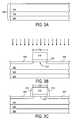
- FIGS. 3A-3Fillustrate a method of fabricating a field effect transistor having a pair of source/drain regions comprising a narrow bandgap semiconductor in accordance with embodiments of the present invention.
- FIG. 4is a plot showing the electron mobility verses sheet carrier concentration for indium antimonide (InSb).
- FIG. 5is an illustration of a nonplanar transistor having a pair of source/drains formed from a narrow bandgap semiconductor.
- FIG. 6illustrates a system in accordance with one embodiment.
- the present inventionis a field effect transistor having a pair of source/drain regions formed from a narrow bandgap semiconductor film.
- Embodiments of the present inventioninclude a field effect transistor having a pair of source/drain regions formed from a narrow energy bandgap (e.g., less than 0.75 eV) semiconductor film.
- the silicon substrate adjacent to the gate electrodeis etched out and refilled with a selective epitaxial regrowth of a narrow bandgap high mobility compound semiconductor material.
- the source and drain regionsfrom a narrow bandgap high conductivity semiconductor, such as indium antimonide (InSb), indium arsenide (InAs), indium gallium arsenide (In 1-x Ga x As(x>50%)) and indium phosphide (InP), a significant reduction in the parasitic series resistance in extremely scaled sub-50 nanometer MOSFETs can be obtained. Additionally, in embodiments of the present invention, non-alloyed ohmic contacts are used to make contact to the narrow bandgap semiconductor film which results in a very low thermal budget in the front end process thereby improving device performance.
- a narrow bandgap high conductivity semiconductorsuch as indium antimonide (InSb), indium arsenide (InAs), indium gallium arsenide (In 1-x Ga x As(x>50%)) and indium phosphide (InP)
- the transistoris formed in a thin silicon layer of silicon-on-insulator (SOI) substrate in order to decrease or remove the possibility of increased junction leakage current.
- SOIsilicon-on-insulator
- Source and drain regions formed from a narrow bandgap semiconductor materialcan be used to decrease the parasitic resistance in both planar and nonplanar devices.
- FIG. 2Ais an example of a metal oxide semiconductor field effect transistor (MOSFET) 200 in accordance with an embodiment of the present invention.
- Transistor 200has a gate electrode 202 formed on a gate dielectric layer 204 formed on a silicon layer 206 .
- a pair of sidewall spacers 208are formed along laterally opposite sidewalls of gate electrode 202 as shown in FIG. 2A .
- Transistor 200has a pair of source/drain regions 210 formed on opposite sides of gate electrode 202 .
- a channel region 206is located in the silicon layer between the source and drain regions 210 .
- the source and drain regions 210are formed from a low or narrow bandgap energy semiconductor film 212 .
- the narrow bandgap semiconductoris an epitaxial or single crystalline film.
- the source and drain regions 210are formed from a narrow bandgap semiconductor 212 having an energy bandgap of less than 0.75 eV and in embodiments less than 0.36 eV.
- the narrow bandgap semiconductor film 212is a compound semiconductor film having a bandgap between 0.75 eV and 0.18 eV.
- the source and drain regions 210include a epitaxial narrow bandgap, high mobility compound semiconductor material 212 , such as but not limited to indium antimonide (InSb), indium arsenide (InAs), indium gallium arsenide (In 1-x Ga x As(x>50%)) and indium phosphide (InP).
- the source and drain region 210are formed from a compound semiconductor 212 having bulk mobility between 10,000-80,000 ⁇ (cm 2 V ⁇ 1 s ⁇ 1 ).
- FIG. 4is a plot which illustrates the electron mobility in InSb vs. the carrier concentration. The higher mobility results in a low sheet resistance (R sd ).
- Another advantage of using a narrow bandgap semiconductor 212 with very high mobilityis that it provides a lower band offset, ⁇ b , and a lower effective electron mass (m*) which results in a lowering of the contact resistivity, ⁇ c, which results in a lower contact resistance, R c , compared to conventional n+implanted silicon source and drain regions with nickel silicide contacts.
- transistor 200has raised source and drain regions. Raised source and drain regions are formed by having the narrow bandgap semiconductor film 212 extend above the top surface 201 of the silicon film upon which the gate dielectric layer 204 is formed. In an embodiment of the present invention, the narrow bandgap semiconductor film 212 of the source and drain regions 210 extends at least 200 ⁇ above the silicon surface 201 and generally between 200-300 ⁇ above the surface 201 . The dielectric sidewall spacers 208 isolate the raised portion of the source and drain regions 210 from the gate electrode 202 .
- the spacers 208are formed to a width sufficient enough to isolate the narrow bandgap semiconductor films from the gate electrode 202 as well as wide enough to reduce the parasitic Miller capacitance which can develop between the raised source and drain regions and the gate electrode 202 . Additionally, spacers 208 should not be formed too wide so that current traversal path is increased and packing density decreased.
- the sidewall spacersare formed from an insulating film, such as silicon nitride or silicon oxide, having a width of between 100-500 ⁇ .
- the narrow bandgap semiconductor 212laterally extends completely beneath spacer 208 and slightly extends beneath or undercuts the gate dielectric/gate electrode 204 / 202 . In an embodiment of the present invention, the narrow bandgap semiconductor 212 extends beneath the outside edges of the gate electrode 210 by approximately 50-70 ⁇ .
- the narrow bandgap semiconductorwhen forming an n type field effect transistor (FET) where the majority carriers are electrons, the narrow bandgap semiconductor is doped to an n type conductivity and when forming a p type field effect transistor where the majority carriers are holes, the narrow bandgap semiconductor 212 is doped to a p type conductivity.
- FETfield effect transistor
- a narrow bandgap semiconductor 212such as indium antimonide (InSb), indium arsenide (InAs), indium gallium arsenide (In 1-x Ga x As(x>50%)) and indium phosphide (InP), can be doped to an n type conductivity with, for example, tellurium (Te), silicon (Si) and sulfur (S) and doped to a p type conductivity with, for example, carbon (C), cadmium (Cd), zinc (Zn) and chromium (Cr).
- InSbindium antimonide
- InAsindium arsenide
- In 1-x Ga x As(x>50%)indium gallium arsenide
- InPindium phosphide
- the source and drain regionscan include a pair of source/drain extensions or tip regions 214 as illustrated in FIG. 2B .
- Source/drain extensionsare a portion of the source/drain regions 210 and are formed by doping the silicon layer and extend beneath the gate electrode and spacers.
- the extensions 214are doped to a p type conductivity for a p type device and to an n type conductivity for a n type device. If the source/drain extensions 214 are provided, then the narrow bandgap semiconductor portion 212 of the source and drain regions 210 , need not extend beneath the outside edges of the gate electrode because the laterally tip regions 214 extend the source and drain regions 210 beneath the spacers 208 and gate electrode 202 as shown in FIG.
- the narrow bandgap semiconductor 212extends only slightly beneath the sidewall spacers 208 where it contacts the source/drain extensions 214 . In yet another embodiment of the present invention, the narrow bandgap semiconductor 212 contacts the source/drain extensions 214 in alignment with the outside edges of the sidewall spacers 208 .
- transistor 200is formed in a silicon layer which is part of a monocrystalline silicon substrate.
- the channel region 206is formed in a doped region of the monocrystalline silicon substrate and the narrow bandgap semiconductor film 210 is formed in recesses formed in the monocrystalline silicon substrate.
- the transistoris sometimes referred to as “a bulk” transistor. Unfortunately, forming the source and drain regions 210 from a low bandgap semiconductor, a bulk device can cause an increase the junction leakage current.
- transistor 200is formed in a thin epitaxial silicon film 220 of a silicon-on-insulator (SOI) substrate 224 .
- a silicon-on-insulator (SOI) substrate 224includes a thin silicon film 220 formed on a buried oxide layer 222 which in turn is formed on a monocrystalline silicon substrate 226 .
- the narrow bandgap semiconductor portions 212 of the source and drain regions 210are formed in recesses formed in the epitaxial silicon film 220 of the SOI substrate 226 .
- a small portion 230 of the epitaxial silicon film 220remains between the buried oxide layer and the bottom of the narrow bandgap semiconductor 212 so that an epitaxial narrow bandgap semiconductor film can be selectively grown on the epitaxial silicon film 220 .
- the portion 230 of the epitaxial silicon film remaining between the buried oxide layer and the narrow bandgap semiconductor film 212is between 10-100 ⁇ thick.
- an interlayer dielectric 240such as but not limited to a silicon dioxide film or a low k dielectric, such as a fluorine doped silicon dioxide (SiOF), a carbon doped oxide (CDO) or a zeolite dielectric, is formed over and around transistor 200 as shown in FIGS. 2A and 2B .
- the interlayer dielectric layer 240isolates transistor 200 from the upper levels of metallization 260 used to interconnect the various transistor 200 formed on substrate 224 into function circuits, such as microprocessors, digital signal processors and memory devices.
- Metal contacts 250are formed through the interlayer dielectric and directly contact the narrow bandgap semiconductor material 212 of the source and drain regions 210 to provide electrical connection between the first level of metallization and the source and drain regions 210 as illustrated in FIG. 2A .
- the metal contacts 250form a low resistance non-alloyed ohmic contact with a narrow bandgap semiconductor 210 .
- metal contacts 250comprise a lower titanium adhesion layer 252 and a bulk gold (Au) layer 254 .
- Aubulk gold
- there is no silicide or alloyed films formed between the narrow bandgap semiconductor film 210 and the contact 250there is no silicide or alloyed films formed between the narrow bandgap semiconductor film 210 and the contact 250 .
- the use of a non-alloyed metal contact 250results in a very low thermal budget in the front end of the process flow and its associated benefits.
- FIG. 5illustrates a tri-gate transistor 500 having source and drain regions comprising a narrow bandgap semiconductor film 212 .
- the silicon filmis first patterned into a silicon body having a top surface opposite a bottom surface formed on buried oxide and a pair of laterally sidewalls as shown in FIG. 5 .
- the gate dielectric layer 204is then formed on the top surface and sidewalls of the silicon body as shown in FIG. 5 .
- a gate electrodeis then formed on the gate dielectric layer on the top surface of a silicon body and directly adjacent to the gate dielectric layer 204 on the sidewalls of the semiconductor body so that the gate electrode 202 surrounds the channel region of the silicon body on three sides.
- the gate electrode 202can be isolated from the silicon body by a thick dielectric layer (not shown) so that the gate only controls two sides of the body.
- the portion of the silicon body on opposite sides of the gate electrode used to form the source and drain regionscan then be partially etched away so that the narrow bandgap semiconductor film 212 can be regrown to form the source and drain regions 210 .
- FIGS. 3A-3Fillustrate a method of forming a field effect transistor having source and drain regions formed from a narrow bandgap semiconductor film in accordance with embodiments of the present invention.
- the fabrication of a transistor in accordance with the present inventionbegins with a substrate.
- the substrateis a monocrystalline silicon substrate, for example, when forming a bulk semiconductor device.
- the monocrystalline silicon substratemay include an epitaxial silicon film formed on the monocrystalline substrate as is well known in the art.
- the substrateis a silicon-on-insulator (SOI), such as substrate 300 as illustrated in FIG. 3A .
- SOIsilicon-on-insulator
- the silicon-on-insulator substrate 300includes an epitaxial silicon film 302 formed on a buried oxide layer 304 which in turn is formed on a monocrystalline silicon substrate 306 .
- the buried oxide layerhas a thickness between 200-2000 ⁇ .
- the epitaxial silicon film or layer 302has a thickness of between 10-400 ⁇ .
- Isolation regionsare typically formed in the silicon film 302 or substrate adjacent to the device fabrication area to isolate the fabricated transistor from adjacent transistors.
- the epitaxial silicon film 302is then doped to a conductivity type and concentration desired for the channel region of the device.
- the silicon filmwhen fabricating a p type transistor, can be doped to an n type conductivity and when fabricating an n type device the silicon film 302 can be doped to a p type conductivity.
- the semiconductor film 302will be doped to an n type or p type conductivity with a concentration level between 1 ⁇ 10 16 -1 ⁇ 10 19 atoms/cm 3 .
- the silicon film 302is left undoped or intrinsic in order to fabricate a transistor with an undoped or intrinsic channel region.
- a gate dielectric layer 308is formed on the epitaxial silicon film 302 and a gate electrode 310 formed on the gate dielectric layer 308 .
- the gate dielectric layercan be a deposited or grown dielectric.
- the gate dielectric layeris a silicon dioxide or a silicon oxynitride dielectric film grown with a wet/dry oxidation process.
- the silicon oxide filmis grown to a thickness between 5-15 ⁇ .
- the gate dielectric layeris a deposited dielectric, such as but not limited to a high dielectric constant film (high k), such as a metal oxide dielectric, such as tantalum pentaoxide, titanium oxide, hafnium oxide, zirconium oxide, aluminum oxide, and various silicates or other high k dielectric, such lead zirconium titanate (PZT) and barium strontium titanate (BST).
- high khigh dielectric constant film
- a high dielectric constant filmcan be formed by any well known technique, such as but not limited to chemical vapor deposition (CVD) and atomic layer deposition (ALD).
- the gate electrode 310can be formed by any well known technique, such as by blanket depositing a gate electrode material over substrate 300 and then utilizing well known photolithography and etching techniques to pattern the gate electrode material into a gate electrode 310 .
- the gate electrode 310has a pair of laterally opposite sidewalls separated by a distance which defines the gate length (Lg) of the transistor.
- gate electrode 310has a gate length (Lg) of less than 50 nanometers.
- the gate electrode 310may be formed from any suitable gate electrode material.
- the gate electrode materialmay comprise a polycrystalline silicon.
- the electrode materialcomprises a polycrystalline silicon germanium alloy.
- the gate electrode materialmay comprise a metal film, such as tungsten, tantalum and their nitrides.
- the gate electrodehas a thickness or height between 200-3000 ⁇ .
- epitaxial silicon film 302when forming a nonplanar transistor, such as a tri-gate or dual gate transistor, epitaxial silicon film 302 would first be patterned into a silicon body having a top surface opposite the buried oxide layer 304 and a pair of laterally opposite sidewalls as is well known in the art.
- the gate dielectric layerWhen forming a tri-gate device, the gate dielectric layer would be formed on the top surface and sidewalls of the fabricated semiconductor body and then the gate electrode formed on and adjacent to the gate dielectric layers so that the gate electrode surrounds the semiconductor body on three sides as is well known in the art.
- a thick insulating layermay be left on the top surface of a semiconductor body to isolate the gate electrode from the top surface of a semiconductor body so that the gate electrode controls only the two sidewalls of the body as is well known in the art.
- source/drain extensions 309may be formed in semiconductor film 302 on opposite sides of gate electrode 310 as shown in FIG. 3B , if desired.
- Source/drain extensions 309can be formed by, for example, ion implanting dopants into the silicon layer 302 .
- the gate electrode 310can act as a mask to prevent the doping of a channel region 320 during the ion implantation process resulting in the formation of source/drain extensions 309 which are formed in alignment with the outside edges of gate electrode 310 .
- a subsequent annealcan be used to cause the dopants to slightly diffusion beneath the outside edges of the gate electrode 310 as shown in FIG. 3B .
- gate electrode 310is a polysilicon gate electrode the source/drain extension implant process can be used to dope the polysilicon film to reduce its resistance.
- the source/drain extensions 309can be used, for example, when the narrow bandgap semiconductor film for the source and drain regions is not extended beneath the gate electrode.
- the source/drain extension formation processmay not be necessary. Omitting the source/drain extension process can help reduce the thermal budget of the front-end process and thereby improve device performance.
- a pair of thin sidewall spacers 312are formed adjacent to the laterally opposite sidewalls of gate electrode 310 .
- Sidewall spacers 312can be formed by blanket depositing a conformal insulating film, such as silicon nitride, silicon oxynitride, or silicon oxide or a combination thereof over substrate 300 and gate electrode 310 and then anisotropically etching back the dielectric film to form spacers 312 .
- the thickness of the deposited dielectric filmdetermines the thickness of the spacers 312 .
- the spacers 312are formed to a thickness between 100-500 ⁇ .
- the spacers 312are formed from a silicon nitride film formed by a hot wall low pressure chemical vapor deposition process (LPCVD).
- LPCVDhot wall low pressure chemical vapor deposition process
- a pair of recesses 316are formed in silicon film 302 on opposite sides of gate electrode 308 as shown in FIG. 3D .
- recesses 316extend beneath the outside edge of gate electrode 310 and gate dielectric layer 308 as shown in FIG. 3D .
- recesses 316extend between approximately 50-70 ⁇ beneath the outside edges of the gate electrode 310 .
- the recessesare formed to a depth of approximately 5-350 ⁇ beneath the surface 301 of silicon film 302 upon which the gate dielectric layer 308 is formed.
- a portion of the silicon film 302remains in recess 316 above buried oxide layer 304 so that narrow bandgap semiconductor film can be subsequently selectively epitaxially grown thereon.
- Any well known and suitable etching techniquecan be utilized to form recesses 316 .
- a selective etch processis used to form recesses 316 .
- an etchantis used which only etches silicon films, such as epitaxial silicon layer 302 and not insulating films such as spacers 310 , gate dielectric 308 and isolations regions.
- gate electrode 310is formed from polycrystalline silicon, an insulating hard mask can be used to form gate electrode 310 then left on during the etching of recesses 316 to protect the silicon electrode from being etched).
- an isotropic etching processessuch as a wet etch, is used to form recesses 316 so that the recess 316 can laterally undercut spacers 312 and gate electrode 310 .
- recesses 316are filled with a narrow bandgap semiconductor film, such as but not limited to indium antimonide (InSb), indium arsenide (InAs), indium gallium arsenide (In 1-x Ga x As(x>50%)) and indium phosphide (InP).
- the narrow bandgap semiconductor 318is deposited to a thickness to fill recess 318 and in another embodiment of the present invention, is deposited to a thickness sufficient to extend above the top surface 301 of silicon film 302 in order to form raised or elevated source and drain regions.
- the narrow bandgap semiconductor filmextends at least 200 ⁇ above top surface 301 of silicon film 302 and in an embodiment of the present invention, extends between 200-500 ⁇ .
- narrow bandgap semiconductor film 318is grown with an epitaxial process, such as but not limited to, molecular beam epitaxy (MBE), metal organic chemical vapor deposition (MOCVD), and low pressure chemical vapor deposition (LPCVD).
- MBEmolecular beam epitaxy
- MOCVDmetal organic chemical vapor deposition
- LPCVDlow pressure chemical vapor deposition
- the narrow bandgap semiconductor film 318is insitu doped (i.e., doped while it is deposited) to an n type or p type conductivity.
- Semiconductor film 318can be doped to an n type conductivity utilizing dopant atoms, such as silicon (Si) or tellurium (Te) and can be doped to a p type conductivity atoms utilizing, for example, carbon (C), cadmium (Cd), zinc (Zn) and chromium (Cr).
- the narrow bandgap semiconductor filmhas a melting temperature between 550-500° C.
- the narrow bandgap semiconductor film 318can be deposited undoped and then subsequently doped by, for example, ion implantation or solid source diffusion.
- the narrow bandgap semiconductor film 318is selectively grown into recesses 316 .
- the narrow bandgap semiconductorforms only on silicon locations, such as epitaxial silicon film in recesses 316 and not on insulating or dielectric layers, such as sidewall spacers 312 and isolation regions.
- gate electrode 310is formed from a polycrystalline silicon or silicon germanium alloy, then an insulating hard mask can be used during the patterning of the gate electrode and left on during the growth of the narrow bandgap semiconductor 318 in order to prevent the formation of a narrow bandgap semiconductor film on the gate electrode.
- the epitaxial silicon film 302 in the lower parts of recesses 316provide a single crystalline lattice from which an epitaxial narrow bandgap semiconductor film can be grown.
- an InSb epitaxial silicon film 318is grown in recess 316 utilizing a MOCVD process utilizing an equimolar gaseous mixture of volatized trimethylindium and stibane (SbH 3 ) with about 5% each by mass in a carrier gas such as argon.
- an indium antimonide (InSb) epitaxial filmis grown utilizing molecular beam epitaxial (MBE) utilizing a solid source.
- non-alloyed ohmic contacts 340are used to electrically couple the source and drain region to the upper levels of metallization 350 .
- an interlayer dielectric (ILD) 330such as but not limited to silicon dioxide (SiO 2 ), fluorine doped silicon dioxide (SiOF) and carbon doped oxide (CDO), is blanket deposited over substrate 300 including gate electrode 310 , spacers 312 and narrow bandgap semiconductor 318 .
- the interlayer dielectric 330is formed to a thickness sufficient to isolate the gate electrode 310 and narrow bandgap semiconductor 318 from the subsequently formed upper level of metallization 350 .
- the interlayer dielectricis formed to a thickness between 500 ⁇ -2000 ⁇ . It is to be appreciated that an interlayer dielectric need not necessarily be a single layer dielectric and can be a composite dielectric layer formed from multiple insulating layers. After depositing the interlayer dielectric, the interlayer dielectric may be planarized to provide a planar top surface.
- contact openingscan then be formed through interlayer dielectric 330 utilizing well known photolithography and etching techniques at locations where contacts 340 are desired to contact the narrow bandgap semiconductor 318 .
- Conductive contacts 340are then formed into the openings and make direct contact with the narrow bandgap semiconductor film 318 .
- contacts 340are formed by blanket depositing a conductive contact film by, for example, chemical vapor deposition (CVD) or atomic layer deposition (ALD) into the openings and onto the top surface of ILD 330 .
- CVDchemical vapor deposition
- ALDatomic layer deposition
- the conductive filmis then removed from the top surface of the ILD by, for example, plasma etch back or chemical mechanical planarization, to form contacts 340 .
- the contactsare formed from a high conductivity metal or metals having a low work function, such as a work function less than 4 eV.
- the contacts 340are bi-layer contacts including a thin adhesion layer 342 and a bulk metal 344 having a high conductivity such as illustrated in FIG. 3F .
- contacts 340include a thin titanium (Ti) adhesion layer of less than 150 ⁇ and a gold (Au) bulk material 344 .
- the contacts 340do not include any alloyed metals or suicides (i.e., metal silicon alloy, such as nickel silicide and titanium silicide). In this way, the thermal budget can remain low and device performance reliability improved.
- upper levels of metallization 350can then be formed in contact with contacts 340 to electrically couple the fabricated transistor with other transistors into functional circuits.
- FIG. 6illustrates a system 600 in accordance with one embodiment.
- system 600includes computing device 602 for processing data.
- Computing device 602may include a motherboard 604 .
- Motherboard 604may include in particular a processor 606 , and a networking interface 608 coupled to a bus 610 .
- processor 606may comprise the device 200 or 500 that has the earlier described narrow bandgap source and drain regions.
- system 600may include other components, including but are not limited to volatile and non-volatile memory, a graphics processor, a digital signal processor, a crypto processor, a chipset, mass storage (such as hard disk, compact disk (CD), digital versatile disk (DVD) and so forth), and so forth.
- volatile and non-volatile memorye.g., volatile and non-volatile memory
- graphics processore.g., graphics processor
- digital signal processore.g., a graphics processor
- crypto processore.g., a graphics processor
- crypto processore.g., a graphics processor
- crypto processore.g., a graphics processor
- crypto processore.g., a graphics processor
- crypto processore.g., a graphics processor
- crypto processore.g., digital signal processor
- chipsete.g., graphics processor, a graphics processor, a digital signal processor, a crypto processor, a chipset, mass storage (such as hard disk, compact disk (CD
- system 600may be a personal digital assistant (PDA), a mobile phone, a tablet computing device, a laptop computing device, a desktop computing device, a set-top box, an entertainment control unit, a digital camera, a digital video recorder, a CD player, a DVD player, or other digital device of the like.
- PDApersonal digital assistant
Landscapes
- Insulated Gate Type Field-Effect Transistor (AREA)
- Chemical & Material Sciences (AREA)
- Crystallography & Structural Chemistry (AREA)
Abstract
Description
- 1. Field of the Invention
- The present invention relates to the field of field effect transistors and more particularly to a field effect transistor having a pair of source/drain regions formed from a narrow bandgap semiconductor film and its method of fabrication.
- 2. Discussion of Related Art
- Integrated circuits, such as microprocessors, digital signal processors, and memory devices are made up of literally millions of transistors coupled together into functional circuits. An example of a conventional metal oxide semiconductor field effect transistor (MOSFET)100 is illustrated in
FIG. 1 .Transistor 100 includes agate electrode 102 formed on a gatedielectric layer 104 which in turn is formed on a monocrystalline silicon substrate. A pair ofsidewall spacers 108 are then formed along laterally opposite sidewalls of thegate electrode 102. A pair of source/drain regions 110 are then formed along opposite sides of thegate electrode 102 as shown inFIG. 1 . The source and drain regions comprise heavily doped portions of thesilicon substrate 106. Typically, asilicide layer 112, such as titanium silicide or nickel silicide, is used to couplecontacts 120 formed in a interlayer dielectric140 to the source anddrain regions 110.Silicide regions 112 are generally formed by alloying a metal, such as titanium, nickel or cobalt with thesilicon substrate 106 to form the metal silicide. Additionally,contacts 120 are generally formed from a relatively high resistance film such as tungsten which can be conformally deposited so that it fills contact opening formed in the intodielectric layer 140. - The dimension of
transistor 100 are continually being scaled down in order to increase packing density and thereby increase the computational power of the fabricated integrated circuits. Unfortunately, astransistor 100 is continually scaled down, the external resistance of the device (Rext) is increased degrading device performance, such as its drive current. Presently, the problem of increased Rext is solved by high active doping of the source and drain region and fully siliciding the source and drain regions. High active doping of the source and drain regions can decrease the electron mobility in the source and drain regions. Fully siliciding the source and drain regions results in a schkotty barrier transistors resulting in ambipolar conduction. Additionally, formation of silicide films by alloying a metal and the semiconductor substrate together can increase the thermal budget of the device which can decrease device performance. FIG. 1 is an illustration of a cross-sectional view of a standard MOS nonplanar field effect transistor.FIGS. 2A and 2B are illustrations of cross-sectional views of nonplanar field effect transistors having a pair of source/drain regions formed from a narrow bandgap semiconductor in accordance with embodiments of the present invention.FIGS. 3A-3F illustrate a method of fabricating a field effect transistor having a pair of source/drain regions comprising a narrow bandgap semiconductor in accordance with embodiments of the present invention.FIG. 4 is a plot showing the electron mobility verses sheet carrier concentration for indium antimonide (InSb).FIG. 5 is an illustration of a nonplanar transistor having a pair of source/drains formed from a narrow bandgap semiconductor.FIG. 6 illustrates a system in accordance with one embodiment.- The present invention is a field effect transistor having a pair of source/drain regions formed from a narrow bandgap semiconductor film. In the following description numerous specific details are set forth in order to provide a thorough understanding of the present invention. In other instances, well known semiconductor processing techniques and equipment have not been forth in particular detail in order to not unnecessarily obscure the present invention.
- Embodiments of the present invention include a field effect transistor having a pair of source/drain regions formed from a narrow energy bandgap (e.g., less than 0.75 eV) semiconductor film. In an embodiment of the present invention, the silicon substrate adjacent to the gate electrode is etched out and refilled with a selective epitaxial regrowth of a narrow bandgap high mobility compound semiconductor material. By forming the source and drain regions from a narrow bandgap high conductivity semiconductor, such as indium antimonide (InSb), indium arsenide (InAs), indium gallium arsenide (In1-xGaxAs(x>50%)) and indium phosphide (InP), a significant reduction in the parasitic series resistance in extremely scaled sub-50 nanometer MOSFETs can be obtained. Additionally, in embodiments of the present invention, non-alloyed ohmic contacts are used to make contact to the narrow bandgap semiconductor film which results in a very low thermal budget in the front end process thereby improving device performance. Additionally, in embodiments of the present invention, the transistor is formed in a thin silicon layer of silicon-on-insulator (SOI) substrate in order to decrease or remove the possibility of increased junction leakage current. Source and drain regions formed from a narrow bandgap semiconductor material can be used to decrease the parasitic resistance in both planar and nonplanar devices.
FIG. 2A is an example of a metal oxide semiconductor field effect transistor (MOSFET)200 in accordance with an embodiment of the present invention.Transistor 200 has agate electrode 202 formed on agate dielectric layer 204 formed on asilicon layer 206. A pair ofsidewall spacers 208 are formed along laterally opposite sidewalls ofgate electrode 202 as shown inFIG. 2A .Transistor 200 has a pair of source/drain regions 210 formed on opposite sides ofgate electrode 202. Achannel region 206 is located in the silicon layer between the source and drainregions 210.- In an embodiment of the present invention, the source and drain
regions 210, or a portion of the source and drainregions 210, are formed from a low or narrow bandgapenergy semiconductor film 212. In an embodiment of the present invention the narrow bandgap semiconductor is an epitaxial or single crystalline film. In an embodiment of the present invention, the source and drainregions 210 are formed from anarrow bandgap semiconductor 212 having an energy bandgap of less than 0.75 eV and in embodiments less than 0.36 eV. In an embodiment of the present invention, the narrowbandgap semiconductor film 212 is a compound semiconductor film having a bandgap between 0.75 eV and 0.18 eV. In an embodiment of the present invention, the source and drainregions 210 include a epitaxial narrow bandgap, high mobilitycompound semiconductor material 212, such as but not limited to indium antimonide (InSb), indium arsenide (InAs), indium gallium arsenide (In1-xGaxAs(x>50%)) and indium phosphide (InP). In an embodiment of the present invention, the source and drainregion 210 are formed from acompound semiconductor 212 having bulk mobility between 10,000-80,000μ (cm2V−1s−1). An advantage of using a narrow bandgap semiconductor in the source and drain regions, is that they have low sheet resistivities due to their inherently high mobilities and superior electron transport properties as compared to silicon.FIG. 4 is a plot which illustrates the electron mobility in InSb vs. the carrier concentration. The higher mobility results in a low sheet resistance (Rsd). Another advantage of using anarrow bandgap semiconductor 212 with very high mobility is that it provides a lower band offset, Øb, and a lower effective electron mass (m*) which results in a lowering of the contact resistivity, ρc, which results in a lower contact resistance, Rc, compared to conventional n+implanted silicon source and drain regions with nickel silicide contacts. - In an embodiment of the present invention,
transistor 200 has raised source and drain regions. Raised source and drain regions are formed by having the narrowbandgap semiconductor film 212 extend above thetop surface 201 of the silicon film upon which thegate dielectric layer 204 is formed. In an embodiment of the present invention, the narrowbandgap semiconductor film 212 of the source and drainregions 210 extends at least 200 Å above thesilicon surface 201 and generally between 200-300 Å above thesurface 201. Thedielectric sidewall spacers 208 isolate the raised portion of the source and drainregions 210 from thegate electrode 202. As such, thespacers 208 are formed to a width sufficient enough to isolate the narrow bandgap semiconductor films from thegate electrode 202 as well as wide enough to reduce the parasitic Miller capacitance which can develop between the raised source and drain regions and thegate electrode 202. Additionally,spacers 208 should not be formed too wide so that current traversal path is increased and packing density decreased. In an embodiment of the present invention, the sidewall spacers are formed from an insulating film, such as silicon nitride or silicon oxide, having a width of between 100-500 Å. - In an embodiment of the present invention, as illustrated in
FIG. 2A , thenarrow bandgap semiconductor 212 laterally extends completely beneathspacer 208 and slightly extends beneath or undercuts the gate dielectric/gate electrode 204/202. In an embodiment of the present invention, thenarrow bandgap semiconductor 212 extends beneath the outside edges of thegate electrode 210 by approximately 50-70 Å. - Additionally, when forming an n type field effect transistor (FET) where the majority carriers are electrons, the narrow bandgap semiconductor is doped to an n type conductivity and when forming a p type field effect transistor where the majority carriers are holes, the
narrow bandgap semiconductor 212 is doped to a p type conductivity. Anarrow bandgap semiconductor 212, such as indium antimonide (InSb), indium arsenide (InAs), indium gallium arsenide (In1-xGaxAs(x>50%)) and indium phosphide (InP), can be doped to an n type conductivity with, for example, tellurium (Te), silicon (Si) and sulfur (S) and doped to a p type conductivity with, for example, carbon (C), cadmium (Cd), zinc (Zn) and chromium (Cr). - In an embodiment of the present invention, the source and drain regions can include a pair of source/drain extensions or
tip regions 214 as illustrated inFIG. 2B . Source/drain extensions are a portion of the source/drain regions 210 and are formed by doping the silicon layer and extend beneath the gate electrode and spacers. Theextensions 214 are doped to a p type conductivity for a p type device and to an n type conductivity for a n type device. If the source/drain extensions 214 are provided, then the narrowbandgap semiconductor portion 212 of the source and drainregions 210, need not extend beneath the outside edges of the gate electrode because thelaterally tip regions 214 extend the source and drainregions 210 beneath thespacers 208 andgate electrode 202 as shown inFIG. 2B . In an embodiment of the present invention, thenarrow bandgap semiconductor 212 extends only slightly beneath thesidewall spacers 208 where it contacts the source/drain extensions 214. In yet another embodiment of the present invention, thenarrow bandgap semiconductor 212 contacts the source/drain extensions 214 in alignment with the outside edges of thesidewall spacers 208. - In an embodiment of the present invention,
transistor 200 is formed in a silicon layer which is part of a monocrystalline silicon substrate. Whentransistor 200 is formed in a monocrystalline silicon substrate, thechannel region 206 is formed in a doped region of the monocrystalline silicon substrate and the narrowbandgap semiconductor film 210 is formed in recesses formed in the monocrystalline silicon substrate. When a transistor is formed in a monocrystalline silicon substrate, the transistor is sometimes referred to as “a bulk” transistor. Unfortunately, forming the source and drainregions 210 from a low bandgap semiconductor, a bulk device can cause an increase the junction leakage current. Accordingly, in an embodiment of the present invention, in order to reduce the junction leakage current,transistor 200 is formed in a thinepitaxial silicon film 220 of a silicon-on-insulator (SOI)substrate 224. A silicon-on-insulator (SOI)substrate 224 includes athin silicon film 220 formed on a buriedoxide layer 222 which in turn is formed on amonocrystalline silicon substrate 226. In an embodiment of the present invention, the narrowbandgap semiconductor portions 212 of the source and drainregions 210 are formed in recesses formed in theepitaxial silicon film 220 of theSOI substrate 226. In an embodiment of the present invention, asmall portion 230 of theepitaxial silicon film 220 remains between the buried oxide layer and the bottom of thenarrow bandgap semiconductor 212 so that an epitaxial narrow bandgap semiconductor film can be selectively grown on theepitaxial silicon film 220. In an embodiment of the present invention, theportion 230 of the epitaxial silicon film remaining between the buried oxide layer and the narrowbandgap semiconductor film 212 is between 10-100 Å thick. - Additionally, in an embodiment of the present invention, an
interlayer dielectric 240, such as but not limited to a silicon dioxide film or a low k dielectric, such as a fluorine doped silicon dioxide (SiOF), a carbon doped oxide (CDO) or a zeolite dielectric, is formed over and aroundtransistor 200 as shown inFIGS. 2A and 2B . Theinterlayer dielectric layer 240 isolatestransistor 200 from the upper levels ofmetallization 260 used to interconnect thevarious transistor 200 formed onsubstrate 224 into function circuits, such as microprocessors, digital signal processors and memory devices.Metal contacts 250 are formed through the interlayer dielectric and directly contact the narrowbandgap semiconductor material 212 of the source and drainregions 210 to provide electrical connection between the first level of metallization and the source and drainregions 210 as illustrated inFIG. 2A . In an embodiment of the present invention, themetal contacts 250 form a low resistance non-alloyed ohmic contact with anarrow bandgap semiconductor 210. In an embodiment of the present invention,metal contacts 250 comprise a lowertitanium adhesion layer 252 and a bulk gold (Au)layer 254. In an embodiment of the present invention, there is no silicide or alloyed films formed between the narrowbandgap semiconductor film 210 and thecontact 250. The use of anon-alloyed metal contact 250 results in a very low thermal budget in the front end of the process flow and its associated benefits. - It is to be appreciated that the present invention is not limited to planar devices and can be used in nonplanar devices, such as tri-gate transistors and dual gate transistors.
FIG. 5 illustrates atri-gate transistor 500 having source and drain regions comprising a narrowbandgap semiconductor film 212. In a nonplanar device, instead of forming thegate dielectric layer 204 on a single surface of a silicon film, the silicon film is first patterned into a silicon body having a top surface opposite a bottom surface formed on buried oxide and a pair of laterally sidewalls as shown inFIG. 5 . Thegate dielectric layer 204 is then formed on the top surface and sidewalls of the silicon body as shown inFIG. 5 . A gate electrode is then formed on the gate dielectric layer on the top surface of a silicon body and directly adjacent to thegate dielectric layer 204 on the sidewalls of the semiconductor body so that thegate electrode 202 surrounds the channel region of the silicon body on three sides. In a FINFET or dual gate device, thegate electrode 202 can be isolated from the silicon body by a thick dielectric layer (not shown) so that the gate only controls two sides of the body. The portion of the silicon body on opposite sides of the gate electrode used to form the source and drain regions can then be partially etched away so that the narrowbandgap semiconductor film 212 can be regrown to form the source and drainregions 210. FIGS. 3A-3F illustrate a method of forming a field effect transistor having source and drain regions formed from a narrow bandgap semiconductor film in accordance with embodiments of the present invention. The fabrication of a transistor in accordance with the present invention begins with a substrate. In an embodiment of the present invention, the substrate is a monocrystalline silicon substrate, for example, when forming a bulk semiconductor device. In an embodiment of the present invention, the monocrystalline silicon substrate may include an epitaxial silicon film formed on the monocrystalline substrate as is well known in the art. In yet another embodiment of the present invention, the substrate is a silicon-on-insulator (SOI), such assubstrate 300 as illustrated inFIG. 3A . In an embodiment of the present invention, the silicon-on-insulator substrate 300 includes anepitaxial silicon film 302 formed on a buriedoxide layer 304 which in turn is formed on amonocrystalline silicon substrate 306. In an embodiment of the present invention, the buried oxide layer has a thickness between 200-2000 Å. Additionally, in an embodiment of the present invention, the epitaxial silicon film orlayer 302 has a thickness of between 10-400 Å.- Isolation regions, not shown, are typically formed in the
silicon film 302 or substrate adjacent to the device fabrication area to isolate the fabricated transistor from adjacent transistors. Theepitaxial silicon film 302 is then doped to a conductivity type and concentration desired for the channel region of the device. In an embodiment of the present invention, when fabricating a p type transistor, the silicon film can be doped to an n type conductivity and when fabricating an n type device thesilicon film 302 can be doped to a p type conductivity. Typically, thesemiconductor film 302 will be doped to an n type or p type conductivity with a concentration level between 1×10¹⁶-1×10¹⁹atoms/cm3. In an embodiment of the present invention, thesilicon film 302 is left undoped or intrinsic in order to fabricate a transistor with an undoped or intrinsic channel region. - Next, as shown in
FIG. 3B , agate dielectric layer 308 is formed on theepitaxial silicon film 302 and agate electrode 310 formed on thegate dielectric layer 308. The gate dielectric layer can be a deposited or grown dielectric. In an embodiment of the present invention, the gate dielectric layer is a silicon dioxide or a silicon oxynitride dielectric film grown with a wet/dry oxidation process. In an embodiment of the present invention, the silicon oxide film is grown to a thickness between 5-15 Å. In an embodiment of the present invention, the gate dielectric layer is a deposited dielectric, such as but not limited to a high dielectric constant film (high k), such as a metal oxide dielectric, such as tantalum pentaoxide, titanium oxide, hafnium oxide, zirconium oxide, aluminum oxide, and various silicates or other high k dielectric, such lead zirconium titanate (PZT) and barium strontium titanate (BST). A high dielectric constant film can be formed by any well known technique, such as but not limited to chemical vapor deposition (CVD) and atomic layer deposition (ALD). - The
gate electrode 310 can be formed by any well known technique, such as by blanket depositing a gate electrode material oversubstrate 300 and then utilizing well known photolithography and etching techniques to pattern the gate electrode material into agate electrode 310. In an embodiment of the present invention, thegate electrode 310 has a pair of laterally opposite sidewalls separated by a distance which defines the gate length (Lg) of the transistor. In an embodiment of the present invention,gate electrode 310 has a gate length (Lg) of less than 50 nanometers. Thegate electrode 310 may be formed from any suitable gate electrode material. In an embodiment of the present invention, the gate electrode material may comprise a polycrystalline silicon. In an embodiment of the present invention, the electrode material comprises a polycrystalline silicon germanium alloy. In yet another embodiment of the present invention, the gate electrode material may comprise a metal film, such as tungsten, tantalum and their nitrides. In an embodiment of the present invention, the gate electrode has a thickness or height between 200-3000 Å. - It is to be appreciated that when forming a nonplanar transistor, such as a tri-gate or dual gate transistor,
epitaxial silicon film 302 would first be patterned into a silicon body having a top surface opposite the buriedoxide layer 304 and a pair of laterally opposite sidewalls as is well known in the art. When forming a tri-gate device, the gate dielectric layer would be formed on the top surface and sidewalls of the fabricated semiconductor body and then the gate electrode formed on and adjacent to the gate dielectric layers so that the gate electrode surrounds the semiconductor body on three sides as is well known in the art. When forming a dual gate or FINFET device, a thick insulating layer may be left on the top surface of a semiconductor body to isolate the gate electrode from the top surface of a semiconductor body so that the gate electrode controls only the two sidewalls of the body as is well known in the art. - Next, after the formation of
gate dielectric layer 308 andgate electrode 310, source/drain extensions 309 may be formed insemiconductor film 302 on opposite sides ofgate electrode 310 as shown inFIG. 3B , if desired. Source/drain extensions 309 can be formed by, for example, ion implanting dopants into thesilicon layer 302. Thegate electrode 310 can act as a mask to prevent the doping of achannel region 320 during the ion implantation process resulting in the formation of source/drain extensions 309 which are formed in alignment with the outside edges ofgate electrode 310. A subsequent anneal can be used to cause the dopants to slightly diffusion beneath the outside edges of thegate electrode 310 as shown inFIG. 3B . Thengate electrode 310 is a polysilicon gate electrode the source/drain extension implant process can be used to dope the polysilicon film to reduce its resistance. The source/drain extensions 309 can be used, for example, when the narrow bandgap semiconductor film for the source and drain regions is not extended beneath the gate electrode. When fabricating a transistor where the narrow bandgap semiconductor laterally extends beneath thegate electrode 310, the source/drain extension formation process may not be necessary. Omitting the source/drain extension process can help reduce the thermal budget of the front-end process and thereby improve device performance. - Next, as shown in
FIG. 3C , a pair ofthin sidewall spacers 312 are formed adjacent to the laterally opposite sidewalls ofgate electrode 310.Sidewall spacers 312 can be formed by blanket depositing a conformal insulating film, such as silicon nitride, silicon oxynitride, or silicon oxide or a combination thereof oversubstrate 300 andgate electrode 310 and then anisotropically etching back the dielectric film to formspacers 312. The thickness of the deposited dielectric film determines the thickness of thespacers 312. In an embodiment of the present invention, thespacers 312 are formed to a thickness between 100-500 Å. In an embodiment of the present invention, thespacers 312 are formed from a silicon nitride film formed by a hot wall low pressure chemical vapor deposition process (LPCVD). - Next, a pair of
recesses 316 are formed insilicon film 302 on opposite sides ofgate electrode 308 as shown inFIG. 3D . In an embodiment of the present invention, recesses316 extend beneath the outside edge ofgate electrode 310 andgate dielectric layer 308 as shown inFIG. 3D . In an embodiment of the present invention, recesses316 extend between approximately 50-70 Å beneath the outside edges of thegate electrode 310. In an embodiment of the present invention, the recesses are formed to a depth of approximately 5-350 Å beneath thesurface 301 ofsilicon film 302 upon which thegate dielectric layer 308 is formed. In an embodiment of the present invention, a portion of thesilicon film 302 remains inrecess 316 above buriedoxide layer 304 so that narrow bandgap semiconductor film can be subsequently selectively epitaxially grown thereon. Any well known and suitable etching technique can be utilized to form recesses316. In an embodiment of the present invention, a selective etch process is used to form recesses316. In a selective etch process, an etchant is used which only etches silicon films, such asepitaxial silicon layer 302 and not insulating films such asspacers 310,gate dielectric 308 and isolations regions. (Ifgate electrode 310 is formed from polycrystalline silicon, an insulating hard mask can be used to formgate electrode 310 then left on during the etching ofrecesses 316 to protect the silicon electrode from being etched). In an embodiment of the present invention, an isotropic etching processes, such as a wet etch, is used to formrecesses 316 so that therecess 316 can laterally undercutspacers 312 andgate electrode 310. In an embodiment of the present invention, recesses316 are formed with a wet etch comprising an ammonium hydroxide or asymmetric or symmetric tetra (alkyl) ammonium hydroxides (alkyl=methyl, ethyl, propyl, isopropyl, butyl, tert-butyl; symmetric meaning all 4 alkyl groups are the same). - Next, as shown in
FIG. 3E , recesses316 are filled with a narrow bandgap semiconductor film, such as but not limited to indium antimonide (InSb), indium arsenide (InAs), indium gallium arsenide (In1-xGaxAs(x>50%)) and indium phosphide (InP). In an embodiment of the present invention, thenarrow bandgap semiconductor 318 is deposited to a thickness to fillrecess 318 and in another embodiment of the present invention, is deposited to a thickness sufficient to extend above thetop surface 301 ofsilicon film 302 in order to form raised or elevated source and drain regions. In an embodiment of the present invention, the narrow bandgap semiconductor film extends at least 200 Å abovetop surface 301 ofsilicon film 302 and in an embodiment of the present invention, extends between 200-500 Å. - Any well known and suitable technique can be used to deposit narrow
bandgap semiconductor film 318. In an embodiment of the present invention, the narrowbandgap semiconductor film 318 is grown with an epitaxial process, such as but not limited to, molecular beam epitaxy (MBE), metal organic chemical vapor deposition (MOCVD), and low pressure chemical vapor deposition (LPCVD). - In embodiment of the present invention, the narrow
bandgap semiconductor film 318 is insitu doped (i.e., doped while it is deposited) to an n type or p type conductivity.Semiconductor film 318 can be doped to an n type conductivity utilizing dopant atoms, such as silicon (Si) or tellurium (Te) and can be doped to a p type conductivity atoms utilizing, for example, carbon (C), cadmium (Cd), zinc (Zn) and chromium (Cr). In an embodiment of the present invention, the narrow bandgap semiconductor film has a melting temperature between 550-500° C. so that it can be deposited at a relatively low temperature, such as less than 500° C., and still enable dopant atoms to substitute into the narrow bandgap semiconductor lattice without requiring an activation anneal. Eliminating an activation anneal reduces the thermal budget of the process used to fabricate the transistor. - In an alternative embodiment of the present invention, the narrow
bandgap semiconductor film 318 can be deposited undoped and then subsequently doped by, for example, ion implantation or solid source diffusion. - In an embodiment of the present invention, the narrow
bandgap semiconductor film 318 is selectively grown intorecesses 316. In a selective deposition process, the narrow bandgap semiconductor forms only on silicon locations, such as epitaxial silicon film inrecesses 316 and not on insulating or dielectric layers, such assidewall spacers 312 and isolation regions. Ifgate electrode 310 is formed from a polycrystalline silicon or silicon germanium alloy, then an insulating hard mask can be used during the patterning of the gate electrode and left on during the growth of thenarrow bandgap semiconductor 318 in order to prevent the formation of a narrow bandgap semiconductor film on the gate electrode. Theepitaxial silicon film 302 in the lower parts ofrecesses 316 provide a single crystalline lattice from which an epitaxial narrow bandgap semiconductor film can be grown. - In an embodiment of the present invention, an InSb
epitaxial silicon film 318 is grown inrecess 316 utilizing a MOCVD process utilizing an equimolar gaseous mixture of volatized trimethylindium and stibane (SbH3) with about 5% each by mass in a carrier gas such as argon. In an embodiment of the present invention, an indium antimonide (InSb) epitaxial film is grown utilizing molecular beam epitaxial (MBE) utilizing a solid source. - In embodiment of the present invention, non-alloyed
ohmic contacts 340 are used to electrically couple the source and drain region to the upper levels ofmetallization 350. Accordingly, first an interlayer dielectric (ILD)330, such as but not limited to silicon dioxide (SiO2), fluorine doped silicon dioxide (SiOF) and carbon doped oxide (CDO), is blanket deposited oversubstrate 300 includinggate electrode 310,spacers 312 andnarrow bandgap semiconductor 318. Theinterlayer dielectric 330 is formed to a thickness sufficient to isolate thegate electrode 310 andnarrow bandgap semiconductor 318 from the subsequently formed upper level ofmetallization 350. In an embodiment of the present invention, the interlayer dielectric is formed to a thickness between 500 Å-2000 Å. It is to be appreciated that an interlayer dielectric need not necessarily be a single layer dielectric and can be a composite dielectric layer formed from multiple insulating layers. After depositing the interlayer dielectric, the interlayer dielectric may be planarized to provide a planar top surface. - Next, contact openings can then be formed through
interlayer dielectric 330 utilizing well known photolithography and etching techniques at locations wherecontacts 340 are desired to contact thenarrow bandgap semiconductor 318.Conductive contacts 340 are then formed into the openings and make direct contact with the narrowbandgap semiconductor film 318. In an embodiment of the present invention,contacts 340 are formed by blanket depositing a conductive contact film by, for example, chemical vapor deposition (CVD) or atomic layer deposition (ALD) into the openings and onto the top surface ofILD 330. The conductive film is then removed from the top surface of the ILD by, for example, plasma etch back or chemical mechanical planarization, to formcontacts 340. In an embodiment of the present invention, the contacts are formed from a high conductivity metal or metals having a low work function, such as a work function less than 4 eV. In an embodiment of the present invention, thecontacts 340 are bi-layer contacts including athin adhesion layer 342 and abulk metal 344 having a high conductivity such as illustrated inFIG. 3F . In an embodiment of the present invention,contacts 340 include a thin titanium (Ti) adhesion layer of less than 150 Å and a gold (Au)bulk material 344. In an embodiment of the present invention, thecontacts 340 do not include any alloyed metals or suicides (i.e., metal silicon alloy, such as nickel silicide and titanium silicide). In this way, the thermal budget can remain low and device performance reliability improved. Next, upper levels ofmetallization 350 can then be formed in contact withcontacts 340 to electrically couple the fabricated transistor with other transistors into functional circuits. - This completes the fabrication of a field effect transistor having source and drain regions formed from a narrow bandgap semiconductor.
FIG. 6 illustrates asystem 600 in accordance with one embodiment. As illustrated, for the embodiment,system 600 includescomputing device 602 for processing data.Computing device 602 may include amotherboard 604.Motherboard 604 may include in particular aprocessor 606, and anetworking interface 608 coupled to abus 610. More specifically,processor 606 may comprise thedevice - Depending on the applications,
system 600 may include other components, including but are not limited to volatile and non-volatile memory, a graphics processor, a digital signal processor, a crypto processor, a chipset, mass storage (such as hard disk, compact disk (CD), digital versatile disk (DVD) and so forth), and so forth. One or more of these components may also include the earlier described narrow bandgap source and drain regions. - In various embodiments,
system 600 may be a personal digital assistant (PDA), a mobile phone, a tablet computing device, a laptop computing device, a desktop computing device, a set-top box, an entertainment control unit, a digital camera, a digital video recorder, a CD player, a DVD player, or other digital device of the like.
Claims (34)
1. A transistor comprising:
a gate electrode formed on a gate dielectric layer formed on a silicon layer; and
a pair of source/drain regions formed on opposite sides of said gate electrode, said pair of source/drain regions comprising a narrow bandgap semiconductor film.
2. The transistor ofclaim 1 wherein said narrow bandgap semiconductor film has energy bandgap of less than 0.7 eV.
3. The transistor ofclaim 2 wherein said narrow bandgap semiconductor film is selected from the group consisting of indium antimonide (InSb), indium arsenide (InAs), indium gallium arsenide (In1-xGaxAs(x>50%)) and indium phosphide (InP).
4. The transistor ofclaim 1 wherein said narrow bandgap semiconductor film has a bulk mobility between 10,000 to 80,000.
5. The transistor ofclaim 1 wherein said narrow bandgap semiconductor film has a melting point of less than 550° C.
6. The transistor ofclaim 1 further comprising a pair of sidewall spacers formed along opposite sides of said gate electrode, and wherein said narrow bandgap semiconductor film is formed adjacent to said sidewalls spacers and above the top surface of said gate dielectric layer.
7. The transistor ofclaim 1 wherein said silicon layer is a portion of a monocrystalline silicon substrate.
8. The transistor ofclaim 1 wherein said silicon layer is an epitaxial silicon film formed on a buried oxide layer formed on a monocrystalline silicon substrate.
9. The transistor ofclaim 1 wherein said pair of source/drain regions have bottom surface in contact with said silicon layer.
10. The transistor ofclaim 1 wherein said narrow bandgap semiconductor film is doped to an n type conductivity.
11. The transistorclaim 1 wherein said narrow bandgap semiconductor film is doped with a dopant selected from the group consisting of Te or Si or S.
12. The semiconductor device ofclaim 1 further comprising a metal contact in direct contact with said narrow bandgap semiconductor film wherein said metal contact comprises a Ti/Au bi-layer contact.
13. The transistor ofclaim 1 wherein said silicon layer is a silicon body having a top surface opposite a bottom surface formed on an insulating substrate, and wherein said gate dielectric is formed on said top surface and said sidewalls of said silicon body and said gate electrode is formed on said gate dielectric on the top surface of said silicon body and adjacent to said gate dielectric layer on said sidewalls of said semiconductor body.
14. A transistor comprising:
a gate dielectric layer formed on a first surface of a silicon layer;
a gate electrode having a pair of laterally opposite sidewalls formed on said gate dielectric layer;
a pair of sidewall spacers formed adjacent to said pair of laterally opposite sidewalls of said gate electrode;
a pair of source/drain regions formed from an epitaxial narrow bandgap semiconductor film having a work function of less than 0.75 eV and a electron mobility greater than 10,000 cm2V−1s−1wherein said narrow bandgap semiconductor extends beneath said gate dielectric layer and has a top surface extending above said first surface of said silicon layer; and
a pair of non-alloyed contacts in direct contact with said low bandgap semiconductor.
15. The transistor ofclaim 14 wherein said low bandgap semiconductor is selected group consisting of indium antimonide (Insb), indium arsenide (InAs), indium gallium arsenide (In1-xGaxAs(x>50%)) and indium phosphide (InP).
16. The transistor ofclaim 14 wherein said contact comprises a bi-layer titanium/gold contact.
17. The transistor ofclaim 14 wherein said low bandgap semiconductor is doped to an n type conductivity with a dopant selected from the group consisting of Te or Si.
18. The transistor ofclaim 14 wherein said low bandgap semiconductor is doped to a p type conductivity and wherein said dopant is carbon.
19. The transistor ofclaim 14 wherein said silicon layer is a portion of a monocrystalline silicon substrate.
20. The transistor ofclaim 14 wherein said silicon layer is an epitaxial silicon film formed on a buried oxide layer formed on a silicon substrate.
21. A method of forming a transistor comprising:
forming a gate electrode on a gate dielectric layer formed on a silicon layer; and
forming a pair of source/drain regions on opposite sides of said gate electrode wherein said pair of source/drain regions comprise a narrow bandgap semiconductor film.
22. The method ofclaim 21 wherein said narrow bandgap semiconductor film is selected from the group consisting of indium antimonide (InSb), indium arsenide (InAs), indium gallium arsenide (In1-xGaxAs(x>50%)) and indium phosphide (InP).
23. The method ofclaim 21 wherein said narrow bandgap semiconductor has a energy bandgap of less than 0.75 eV.
24. A method of forming a transistor comprising:
forming a gate dielectric layer on a first surface of a silicon layer;
forming a gate electrode on said gate dielectric layer, said gate electrode having a pair of laterally opposite sidewalls;
forming a pair of sidewall spacers adjacent to said sidewalls of said gate electrode;
etching a pair of recesses into said silicon layer adjacent to said outside edges of said sidewall spacers and beneath said gate electrode formed on said gate dielectric layer; and
depositing a narrow bandgap semiconductor film in said recesses.
25. The method ofclaim 24 wherein said narrow bandgap semiconductor has an energy bandgap of less than 0.75 eV.
26. The method ofclaim 24 wherein said narrow bandgap semiconductor film is deposited at a temperature less than 550° C.
27. The method ofclaim 24 wherein said narrow bandgap semiconductor film is deposited in said recesses until said narrow bandgap semiconductor film extends above said first surface.
28. The method ofclaim 24 wherein said narrow bandgap semiconductor film is doped to an n type conductivity while depositing said narrow bandgap semiconductor film.
29. The method ofclaim 24 wherein said low bandgap semiconductor film is doped to a p type conductivity while depositing said low bandgap semiconductor film.
30. The method ofclaim 24 further comprises a step of forming a non-alloy contact onto said low bandgap semiconductor film.
31. The method ofclaim 30 further comprising forming a contact comprising titanium/gold in direct contact with said low bandgap semiconductor film.
32. The method ofclaim 24 wherein said recesses are etched with a wet etchant comprising an ammonium hydroxide or asyemmtric or symmetric tetra (alkyl) ammonium hydroxides (alkyl=methyl, ethyl, propyl, isopropyl, butyl, tert-butyl; symmetric meaning all 4 alkyl groups are the same.
33. The method ofclaim 24 wherein said narrow bandgap semiconductor film is a selectively grown epitaxial film.
34. The method ofclaim 33 wherein said narrow bandgap semiconductor is indium antimonide (InSb) grown by a MOCVD process utilizing an equimolar gaseous mixture of volatized trimethylindium and stibane (SbH3) with about 5% each by mass in a carrier gas such as argon.
Priority Applications (12)
| Application Number | Priority Date | Filing Date | Title |
|---|---|---|---|
| US11/064,996US7518196B2 (en) | 2005-02-23 | 2005-02-23 | Field effect transistor with narrow bandgap source and drain regions and method of fabrication |
| US12/343,400US7825481B2 (en) | 2005-02-23 | 2008-12-23 | Field effect transistor with narrow bandgap source and drain regions and method of fabrication |
| US12/850,582US7893506B2 (en) | 2005-02-23 | 2010-08-04 | Field effect transistor with narrow bandgap source and drain regions and method of fabrication |
| US13/021,640US8183646B2 (en) | 2005-02-23 | 2011-02-04 | Field effect transistor with narrow bandgap source and drain regions and method of fabrication |
| US13/453,403US8368135B2 (en) | 2005-02-23 | 2012-04-23 | Field effect transistor with narrow bandgap source and drain regions and method of fabrication |
| US13/752,272US8664694B2 (en) | 2005-02-23 | 2013-01-28 | Field effect transistor with narrow bandgap source and drain regions and method of fabrication |
| US14/137,804US8816394B2 (en) | 2005-02-23 | 2013-12-20 | Field effect transistor with narrow bandgap source and drain regions and method of fabrication |
| US14/465,636US9048314B2 (en) | 2005-02-23 | 2014-08-21 | Field effect transistor with narrow bandgap source and drain regions and method of fabrication |
| US14/702,608US9368583B2 (en) | 2005-02-23 | 2015-05-01 | Field effect transistor with narrow bandgap source and drain regions and method of fabrication |
| US15/179,884US9614083B2 (en) | 2005-02-23 | 2016-06-10 | Field effect transistor with narrow bandgap source and drain regions and method of fabrication |
| US15/442,087US9748391B2 (en) | 2005-02-23 | 2017-02-24 | Field effect transistor with narrow bandgap source and drain regions and method of fabrication |
| US15/660,574US10121897B2 (en) | 2005-02-23 | 2017-07-26 | Field effect transistor with narrow bandgap source and drain regions and method of fabrication |
Applications Claiming Priority (1)
| Application Number | Priority Date | Filing Date | Title |
|---|---|---|---|
| US11/064,996US7518196B2 (en) | 2005-02-23 | 2005-02-23 | Field effect transistor with narrow bandgap source and drain regions and method of fabrication |
Related Child Applications (1)
| Application Number | Title | Priority Date | Filing Date |
|---|---|---|---|
| US12/343,400DivisionUS7825481B2 (en) | 2005-02-23 | 2008-12-23 | Field effect transistor with narrow bandgap source and drain regions and method of fabrication |
Publications (2)
| Publication Number | Publication Date |
|---|---|
| US20060186484A1true US20060186484A1 (en) | 2006-08-24 |
| US7518196B2 US7518196B2 (en) | 2009-04-14 |
Family
ID=36911787
Family Applications (12)
| Application Number | Title | Priority Date | Filing Date |
|---|---|---|---|
| US11/064,996Active2025-11-16US7518196B2 (en) | 2005-02-23 | 2005-02-23 | Field effect transistor with narrow bandgap source and drain regions and method of fabrication |
| US12/343,400Expired - LifetimeUS7825481B2 (en) | 2005-02-23 | 2008-12-23 | Field effect transistor with narrow bandgap source and drain regions and method of fabrication |
| US12/850,582Expired - LifetimeUS7893506B2 (en) | 2005-02-23 | 2010-08-04 | Field effect transistor with narrow bandgap source and drain regions and method of fabrication |
| US13/021,640Expired - Fee RelatedUS8183646B2 (en) | 2005-02-23 | 2011-02-04 | Field effect transistor with narrow bandgap source and drain regions and method of fabrication |
| US13/453,403Expired - Fee RelatedUS8368135B2 (en) | 2005-02-23 | 2012-04-23 | Field effect transistor with narrow bandgap source and drain regions and method of fabrication |
| US13/752,272Expired - LifetimeUS8664694B2 (en) | 2005-02-23 | 2013-01-28 | Field effect transistor with narrow bandgap source and drain regions and method of fabrication |
| US14/137,804Expired - LifetimeUS8816394B2 (en) | 2005-02-23 | 2013-12-20 | Field effect transistor with narrow bandgap source and drain regions and method of fabrication |
| US14/465,636Expired - Fee RelatedUS9048314B2 (en) | 2005-02-23 | 2014-08-21 | Field effect transistor with narrow bandgap source and drain regions and method of fabrication |
| US14/702,608Expired - LifetimeUS9368583B2 (en) | 2005-02-23 | 2015-05-01 | Field effect transistor with narrow bandgap source and drain regions and method of fabrication |
| US15/179,884Expired - Fee RelatedUS9614083B2 (en) | 2005-02-23 | 2016-06-10 | Field effect transistor with narrow bandgap source and drain regions and method of fabrication |
| US15/442,087Expired - Fee RelatedUS9748391B2 (en) | 2005-02-23 | 2017-02-24 | Field effect transistor with narrow bandgap source and drain regions and method of fabrication |
| US15/660,574Expired - LifetimeUS10121897B2 (en) | 2005-02-23 | 2017-07-26 | Field effect transistor with narrow bandgap source and drain regions and method of fabrication |
Family Applications After (11)
| Application Number | Title | Priority Date | Filing Date |
|---|---|---|---|
| US12/343,400Expired - LifetimeUS7825481B2 (en) | 2005-02-23 | 2008-12-23 | Field effect transistor with narrow bandgap source and drain regions and method of fabrication |
| US12/850,582Expired - LifetimeUS7893506B2 (en) | 2005-02-23 | 2010-08-04 | Field effect transistor with narrow bandgap source and drain regions and method of fabrication |
| US13/021,640Expired - Fee RelatedUS8183646B2 (en) | 2005-02-23 | 2011-02-04 | Field effect transistor with narrow bandgap source and drain regions and method of fabrication |
| US13/453,403Expired - Fee RelatedUS8368135B2 (en) | 2005-02-23 | 2012-04-23 | Field effect transistor with narrow bandgap source and drain regions and method of fabrication |
| US13/752,272Expired - LifetimeUS8664694B2 (en) | 2005-02-23 | 2013-01-28 | Field effect transistor with narrow bandgap source and drain regions and method of fabrication |
| US14/137,804Expired - LifetimeUS8816394B2 (en) | 2005-02-23 | 2013-12-20 | Field effect transistor with narrow bandgap source and drain regions and method of fabrication |
| US14/465,636Expired - Fee RelatedUS9048314B2 (en) | 2005-02-23 | 2014-08-21 | Field effect transistor with narrow bandgap source and drain regions and method of fabrication |
| US14/702,608Expired - LifetimeUS9368583B2 (en) | 2005-02-23 | 2015-05-01 | Field effect transistor with narrow bandgap source and drain regions and method of fabrication |
| US15/179,884Expired - Fee RelatedUS9614083B2 (en) | 2005-02-23 | 2016-06-10 | Field effect transistor with narrow bandgap source and drain regions and method of fabrication |
| US15/442,087Expired - Fee RelatedUS9748391B2 (en) | 2005-02-23 | 2017-02-24 | Field effect transistor with narrow bandgap source and drain regions and method of fabrication |
| US15/660,574Expired - LifetimeUS10121897B2 (en) | 2005-02-23 | 2017-07-26 | Field effect transistor with narrow bandgap source and drain regions and method of fabrication |
Country Status (1)
| Country | Link |
|---|---|
| US (12) | US7518196B2 (en) |
Cited By (32)
| Publication number | Priority date | Publication date | Assignee | Title |
|---|---|---|---|---|
| US20050272187A1 (en)* | 2002-07-12 | 2005-12-08 | Anand Murthy | Process for ultra-thin body SOI devices that incorporate EPI silicon tips and article made thereby |
| US20070134859A1 (en)* | 2005-12-14 | 2007-06-14 | Intel Corporation | Strained silicon MOS device with box layer between the source and drain regions |
| US20070161170A1 (en)* | 2005-12-16 | 2007-07-12 | Orlowski Marius K | Transistor with immersed contacts and methods of forming thereof |
| US20080017891A1 (en)* | 2006-06-30 | 2008-01-24 | Suman Datta | Pinning layer for low resistivity n-type source drain ohmic contacts |
| WO2008033982A3 (en)* | 2006-09-15 | 2008-06-05 | Ibm | Field effect transistor with raised source/drain fin straps |
| US20080274600A1 (en)* | 2007-05-04 | 2008-11-06 | Freescale Semiconductor, Inc. | Method to improve source/drain parasitics in vertical devices |
| US20100078684A1 (en)* | 2008-04-30 | 2010-04-01 | Willy Rachmady | Selective high-k dielectric film deposition for semiconductor device |
| US20100151648A1 (en)* | 2007-08-29 | 2010-06-17 | Taiwan Semiconductor Manufacturing Company,Ltd. | Strained Channel Transistor |
| US20100155846A1 (en)* | 2008-12-19 | 2010-06-24 | Niloy Mukherjee | Metal-insulator-semiconductor tunneling contacts |
| US20100207180A1 (en)* | 2009-02-19 | 2010-08-19 | Kyungpook National University Industry-Academic Cooperation Foundation | High-performance one-transistor floating-body dram cell device |
| US20110101305A1 (en)* | 2006-09-15 | 2011-05-05 | Taiwan Semiconductor Manufacturing Company, Ltd. | MOS Devices with Partial Stressor Channel |
| US20110175174A1 (en)* | 2009-06-05 | 2011-07-21 | Infineon Technologies Ag | Methods of Manufacturing Resistors and Structures Thereof |
| US20120049276A1 (en)* | 2007-10-16 | 2012-03-01 | Semiconductor Energy Laboratory Co., Ltd. | Semiconductor device and manufacturing method thereof |
| US20120056275A1 (en)* | 2010-09-07 | 2012-03-08 | International Business Machines Corporation | High performance low power bulk fet device and method of manufacture |
| CN102544009A (en)* | 2010-12-08 | 2012-07-04 | 中国科学院微电子研究所 | High-mobility CMOS (complementary Metal oxide semiconductor) integrated unit |
| US20130032897A1 (en)* | 2011-08-02 | 2013-02-07 | International Business Machines Corporation | Mosfet gate electrode employing arsenic-doped silicon-germanium alloy layer |
| KR20140127725A (en)* | 2013-04-25 | 2014-11-04 | 삼성전자주식회사 | Method for fabricating fin fet |
| US20150041856A1 (en)* | 2013-08-07 | 2015-02-12 | International Business Machines Corporation | Compound Semiconductor Integrated Circuit and Method to Fabricate Same |
| WO2015047264A1 (en) | 2013-09-26 | 2015-04-02 | Intel Corporation | Methods of forming low band gap source and drain structures in microelectronic devices |
| US20150236100A1 (en)* | 2005-02-23 | 2015-08-20 | Intel Corporation | Field effect transistor with narrow bandgap source and drain regions and method of fabrication |
| US20150279991A1 (en)* | 2010-11-03 | 2015-10-01 | Samsung Electronics Co., Ltd. | Semiconductor devices and methods of manufacturing the same |
| CN105304488A (en)* | 2014-05-29 | 2016-02-03 | 中芯国际集成电路制造(上海)有限公司 | Forming method of fin field effect transistor |
| US20160049483A1 (en)* | 2014-08-15 | 2016-02-18 | Taiwan Semiconductor Manufacturing Company Ltd. | Semiconductor structure and manufacuting method of the same |
| US20170117278A1 (en)* | 2012-06-22 | 2017-04-27 | Samsung Electronics Co., Ltd. | Semiconductor device with impurity-doped region and method of fabricating the same |
| US20180277653A1 (en)* | 2017-03-21 | 2018-09-27 | Semiconductor Manufacturing International (Shanghai) Corporation | Semiconductor structure and fabrication method thereof |
| US20180323260A1 (en)* | 2015-12-23 | 2018-11-08 | Intel Corporation | Dual threshold voltage (vt) channel devices and their methods of fabrication |
| US10366997B2 (en) | 2015-04-01 | 2019-07-30 | Samsung Electronics Co., Ltd. | Semiconductor devices and methods for manufacturing the same |
| US20190378929A1 (en)* | 2014-12-30 | 2019-12-12 | International Business Machines Corporation | Charge carrier transport facilitated by strain |
| US10930781B2 (en)* | 2017-11-29 | 2021-02-23 | Taiwan Semiconductor Manufacturing Co. Ltd. | P-type strained channel in a fin field effect transistor (FinFET) device |
| US11101377B2 (en)* | 2018-03-28 | 2021-08-24 | Intel Corporation | Transistor device with heterogeneous channel structure bodies and method of providing same |
| US11271013B2 (en)* | 2015-11-13 | 2022-03-08 | Semiconductor Energy Laboratory Co., Ltd. | Semiconductor device including a plug |
| CN118782466A (en)* | 2024-09-09 | 2024-10-15 | 四川师范大学 | A silicon-based semiconductor field effect transistor with ultra-low contact resistance and a method for preparing the same |
Families Citing this family (60)
| Publication number | Priority date | Publication date | Assignee | Title |
|---|---|---|---|---|
| US8994104B2 (en) | 1999-09-28 | 2015-03-31 | Intel Corporation | Contact resistance reduction employing germanium overlayer pre-contact metalization |
| US7307348B2 (en) | 2005-12-07 | 2007-12-11 | Micron Technology, Inc. | Semiconductor components having through wire interconnects (TWI) |
| US7999251B2 (en) | 2006-09-11 | 2011-08-16 | International Business Machines Corporation | Nanowire MOSFET with doped epitaxial contacts for source and drain |
| US7629247B2 (en)* | 2007-04-12 | 2009-12-08 | Sandisk 3D Llc | Method of fabricating a self-aligning damascene memory structure |
| US8450165B2 (en) | 2007-05-14 | 2013-05-28 | Intel Corporation | Semiconductor device having tipless epitaxial source/drain regions |
| KR101448899B1 (en)* | 2007-06-12 | 2014-10-13 | 가부시키가이샤 한도오따이 에네루기 켄큐쇼 | Capacitor-less memory |
| US7888734B2 (en)* | 2008-12-04 | 2011-02-15 | Taiwan Semiconductor Manufacturing Company, Ltd. | High-voltage MOS devices having gates extending into recesses of substrates |
| JP2010186877A (en)* | 2009-02-12 | 2010-08-26 | Renesas Electronics Corp | Semiconductor device, and method of manufacturing the same |
| US9245805B2 (en)* | 2009-09-24 | 2016-01-26 | Taiwan Semiconductor Manufacturing Company, Ltd. | Germanium FinFETs with metal gates and stressors |
| US8455334B2 (en) | 2009-12-04 | 2013-06-04 | International Business Machines Corporation | Planar and nanowire field effect transistors |
| US8173993B2 (en)* | 2009-12-04 | 2012-05-08 | International Business Machines Corporation | Gate-all-around nanowire tunnel field effect transistors |
| US8129247B2 (en) | 2009-12-04 | 2012-03-06 | International Business Machines Corporation | Omega shaped nanowire field effect transistors |
| US8384065B2 (en)* | 2009-12-04 | 2013-02-26 | International Business Machines Corporation | Gate-all-around nanowire field effect transistors |
| US8143113B2 (en)* | 2009-12-04 | 2012-03-27 | International Business Machines Corporation | Omega shaped nanowire tunnel field effect transistors fabrication |
| US8598003B2 (en) | 2009-12-21 | 2013-12-03 | Intel Corporation | Semiconductor device having doped epitaxial region and its methods of fabrication |
| US8313999B2 (en)* | 2009-12-23 | 2012-11-20 | Intel Corporation | Multi-gate semiconductor device with self-aligned epitaxial source and drain |
| US8722492B2 (en) | 2010-01-08 | 2014-05-13 | International Business Machines Corporation | Nanowire pin tunnel field effect devices |
| US8372755B2 (en)* | 2010-01-13 | 2013-02-12 | Taiwan Semiconductor Manufacturing Company, Ltd. | Multilayer hard mask |
| US8324940B2 (en) | 2010-04-13 | 2012-12-04 | International Business Machines Corporation | Nanowire circuits in matched devices |
| US8361907B2 (en) | 2010-05-10 | 2013-01-29 | International Business Machines Corporation | Directionally etched nanowire field effect transistors |
| US8324030B2 (en) | 2010-05-12 | 2012-12-04 | International Business Machines Corporation | Nanowire tunnel field effect transistors |
| US8860223B1 (en) | 2010-07-15 | 2014-10-14 | Micron Technology, Inc. | Resistive random access memory |
| US8835231B2 (en) | 2010-08-16 | 2014-09-16 | International Business Machines Corporation | Methods of forming contacts for nanowire field effect transistors |
| US8536563B2 (en) | 2010-09-17 | 2013-09-17 | International Business Machines Corporation | Nanowire field effect transistors |
| US8563386B2 (en) | 2010-11-16 | 2013-10-22 | Globalfoundries Singapore Pte. Ltd. | Integrated circuit system with bandgap material and method of manufacture thereof |
| US8288758B2 (en) | 2010-12-02 | 2012-10-16 | International Business Machines Corporation | SOI SiGe-base lateral bipolar junction transistor |
| US8901537B2 (en) | 2010-12-21 | 2014-12-02 | Intel Corporation | Transistors with high concentration of boron doped germanium |
| US9484432B2 (en) | 2010-12-21 | 2016-11-01 | Intel Corporation | Contact resistance reduction employing germanium overlayer pre-contact metalization |
| US8962400B2 (en) | 2011-07-07 | 2015-02-24 | Taiwan Semiconductor Manufacturing Company, Ltd. | In-situ doping of arsenic for source and drain epitaxy |
| US8383485B2 (en)* | 2011-07-13 | 2013-02-26 | Taiwan Semiconductor Manufacturing Co., Ltd. | Epitaxial process for forming semiconductor devices |
| CN102983079B (en)* | 2011-09-06 | 2017-12-19 | 联华电子股份有限公司 | semiconductor process |
| KR101891458B1 (en) | 2011-12-20 | 2018-08-24 | 인텔 코포레이션 | Semiconductor device having iii-v semiconductor material layer |
| US8643120B2 (en) | 2012-01-06 | 2014-02-04 | International Business Machines Corporation | FinFET with fully silicided gate |
| WO2013112702A1 (en) | 2012-01-26 | 2013-08-01 | Applied Materials, Inc. | Devices including metal-silicon contacts using indium arsenide films and apparatus and methods |
| US8785285B2 (en)* | 2012-03-08 | 2014-07-22 | Taiwan Semiconductor Manufacturing Company, Ltd. | Semiconductor devices and methods of manufacture thereof |
| US9142400B1 (en) | 2012-07-17 | 2015-09-22 | Stc.Unm | Method of making a heteroepitaxial layer on a seed area |
| CN102790096A (en)* | 2012-07-20 | 2012-11-21 | 京东方科技集团股份有限公司 | Film transistor as well as manufacturing method thereof, array substrate and display equipment |
| US9634000B2 (en)* | 2013-03-14 | 2017-04-25 | International Business Machines Corporation | Partially isolated fin-shaped field effect transistors |
| US20160035839A1 (en)* | 2013-03-25 | 2016-02-04 | Asahi Kasei Microdevices Corporation | Compound semiconductor stack and semiconductor device |
| CN105027291A (en) | 2013-03-29 | 2015-11-04 | 英特尔公司 | Transistor architecture with extended recessed spacers and source/drain regions and method of fabrication thereof |
| US8963259B2 (en) | 2013-05-31 | 2015-02-24 | Globalfoundries Inc. | Device isolation in finFET CMOS |
| US9070770B2 (en) | 2013-08-27 | 2015-06-30 | International Business Machines Corporation | Low interfacial defect field effect transistor |
| US9224866B2 (en) | 2013-08-27 | 2015-12-29 | Globalfoundries Inc. | Suspended body field effect transistor |
| US9484460B2 (en)* | 2013-09-19 | 2016-11-01 | Taiwan Semiconductor Manufacturing Company Limited | Semiconductor device having gate dielectric surrounding at least some of channel region and gate electrode surrounding at least some of gate dielectric |
| US9245742B2 (en) | 2013-12-18 | 2016-01-26 | Asm Ip Holding B.V. | Sulfur-containing thin films |
| US9136357B1 (en) | 2014-03-05 | 2015-09-15 | International Business Machines Corporation | Fabrication process for mitigating external resistance and interface state density in a multigate device |
| US9484463B2 (en) | 2014-03-05 | 2016-11-01 | International Business Machines Corporation | Fabrication process for mitigating external resistance of a multigate device |
| US9679990B2 (en)* | 2014-08-08 | 2017-06-13 | Globalfoundries Inc. | Semiconductor structure(s) with extended source/drain channel interfaces and methods of fabrication |
| WO2016186648A1 (en)* | 2015-05-18 | 2016-11-24 | Intel Corporation | Apparatus and method for fabricating a high density memory array |
| US9711396B2 (en)* | 2015-06-16 | 2017-07-18 | Asm Ip Holding B.V. | Method for forming metal chalcogenide thin films on a semiconductor device |
| US9741815B2 (en) | 2015-06-16 | 2017-08-22 | Asm Ip Holding B.V. | Metal selenide and metal telluride thin films for semiconductor device applications |
| CN108028280B (en)* | 2015-09-25 | 2023-04-04 | 英特尔公司 | Method for manufacturing wound source/drain electrode of contact part of back side metal |
| US9564370B1 (en)* | 2015-10-20 | 2017-02-07 | International Business Machines Corporation | Effective device formation for advanced technology nodes with aggressive fin-pitch scaling |
| US9997632B2 (en)* | 2015-12-15 | 2018-06-12 | Taiwan Semiconductor Manufacturing Co., Ltd. | Fin-type field effect transistor device and manufacturing method thereof |
| US9917164B1 (en) | 2017-04-07 | 2018-03-13 | International Business Machines Corporation | Fabricating raised source drain contacts of a CMOS structure |
| WO2019054993A1 (en)* | 2017-09-12 | 2019-03-21 | Intel Corporation | Ferroelectric field effect transistors (fefets) having ambipolar channels |
| US10319855B2 (en) | 2017-09-25 | 2019-06-11 | International Business Machines Corporation | Reducing series resistance between source and/or drain regions and a channel region |
| US10586853B2 (en) | 2017-11-27 | 2020-03-10 | International Business Machines Corporation | Non-planar field effect transistor devices with wrap-around source/drain contacts |
| US10431502B1 (en) | 2018-04-16 | 2019-10-01 | International Business Machines Corporation | Maskless epitaxial growth of phosphorus-doped Si and boron-doped SiGe (Ge) for advanced source/drain contact |
| CN109553415B (en)* | 2019-01-24 | 2021-04-20 | 哈尔滨工业大学 | Preparation method of silicon-doped lead zirconate titanate non-oriented film with high electrothermal effect |
Citations (90)
| Publication number | Priority date | Publication date | Assignee | Title |
|---|---|---|---|---|
| US4905063A (en)* | 1988-06-21 | 1990-02-27 | American Telephone And Telegraph Company, At&T Bell Laboratories | Floating gate memories |
| US4906589A (en)* | 1989-02-06 | 1990-03-06 | Industrial Technology Research Institute | Inverse-T LDDFET with self-aligned silicide |
| US4996574A (en)* | 1988-07-01 | 1991-02-26 | Fujitsu Limited | MIS transistor structure for increasing conductance between source and drain regions |
| US5124777A (en)* | 1990-07-02 | 1992-06-23 | Samsung Electronics Co., Ltd. | Dielectric medium for capacitor of semiconductor device |
| US5179037A (en)* | 1991-12-24 | 1993-01-12 | Texas Instruments Incorporated | Integration of lateral and vertical quantum well transistors in the same epitaxial stack |
| US5216271A (en)* | 1990-09-28 | 1993-06-01 | Kabushiki Kaisha Toshiba | BiCMOS device with low bandgap CMOS contact regions and low bandgap bipolar base region |
| US5391506A (en)* | 1992-01-31 | 1995-02-21 | Kawasaki Steel Corporation | Manufacturing method for semiconductor devices with source/drain formed in substrate projection. |
| US5521859A (en)* | 1991-03-20 | 1996-05-28 | Fujitsu Limited | Semiconductor memory device having thin film transistor and method of producing the same |
| US5716879A (en)* | 1994-12-15 | 1998-02-10 | Goldstar Electron Company, Ltd. | Method of making a thin film transistor |
| US5739544A (en)* | 1993-05-26 | 1998-04-14 | Matsushita Electric Industrial Co., Ltd. | Quantization functional device utilizing a resonance tunneling effect and method for producing the same |
| US5770513A (en)* | 1993-02-25 | 1998-06-23 | Mitsubishi Denki Kabushiki Kaisha | Method for producing semiconductor device with heat dissipation structure |
| US5773331A (en)* | 1996-12-17 | 1998-06-30 | International Business Machines Corporation | Method for making single and double gate field effect transistors with sidewall source-drain contacts |
| US5888309A (en)* | 1997-12-29 | 1999-03-30 | Taiwan Semiconductor Manufacturing Company, Ltd. | Lateral etch inhibited multiple for forming a via through a microelectronics layer susceptible to etching within a fluorine containing plasma followed by an oxygen containing plasma |
| US5899710A (en)* | 1995-01-20 | 1999-05-04 | Sony Corporation | Method for forming field effect transistor having multiple gate electrodes surrounding the channel region |
| US5905285A (en)* | 1996-09-12 | 1999-05-18 | Advanced Micro Devices, Inc. | Ultra short trench transistors and process for making same |
| US6018176A (en)* | 1995-05-26 | 2000-01-25 | Samsung Electronics Co., Ltd. | Vertical transistor and memory cell |
| US6066869A (en)* | 1997-10-06 | 2000-05-23 | Micron Technology, Inc. | Circuit and method for a folded bit line memory cell with vertical transistor and trench capacitor |
| US6087208A (en)* | 1998-03-31 | 2000-07-11 | Advanced Micro Devices, Inc. | Method for increasing gate capacitance by using both high and low dielectric gate material |
| US6252284B1 (en)* | 1999-12-09 | 2001-06-26 | International Business Machines Corporation | Planarized silicon fin device |
| US6251729B1 (en)* | 1998-12-18 | 2001-06-26 | U.S. Philips Corporation | Method of manufacturing a nonvolatile memory |
| US6335251B2 (en)* | 1998-05-29 | 2002-01-01 | Kabushiki Kaisha Toshiba | Semiconductor apparatus having elevated source and drain structure and manufacturing method therefor |
| US20020011612A1 (en)* | 2000-07-31 | 2002-01-31 | Kabushiki Kaisha Toshiba | Semiconductor device and method for manufacturing the same |
| US6358800B1 (en)* | 2000-09-18 | 2002-03-19 | Vanguard International Semiconductor Corporation | Method of forming a MOSFET with a recessed-gate having a channel length beyond photolithography limit |
| US6359311B1 (en)* | 2001-01-17 | 2002-03-19 | Taiwan Semiconductor Manufacturing Co., Ltd. | Quasi-surrounding gate and a method of fabricating a silicon-on-insulator semiconductor device with the same |
| US20020036290A1 (en)* | 2000-09-28 | 2002-03-28 | Kabushiki Kaisha Toshiba | Semiconductor device having MIS field effect transistors or three-dimensional structure |
| US6376317B1 (en)* | 1998-03-30 | 2002-04-23 | Micron Technology, Inc. | Methods for dual-gated transistors |
| US6391782B1 (en)* | 2000-06-20 | 2002-05-21 | Advanced Micro Devices, Inc. | Process for forming multiple active lines and gate-all-around MOSFET |
| US6396108B1 (en)* | 2000-11-13 | 2002-05-28 | Advanced Micro Devices, Inc. | Self-aligned double gate silicon-on-insulator (SOI) device |
| US6407442B2 (en)* | 1994-10-28 | 2002-06-18 | Canon Kabushiki Kaisha | Semiconductor device, and operating device, signal converter, and signal processing system using the same semiconductor device |
| US20020081794A1 (en)* | 2000-12-26 | 2002-06-27 | Nec Corporation | Enhanced deposition control in fabricating devices in a semiconductor wafer |
| US6413877B1 (en)* | 2000-12-22 | 2002-07-02 | Lam Research Corporation | Method of preventing damage to organo-silicate-glass materials during resist stripping |
| US6413802B1 (en)* | 2000-10-23 | 2002-07-02 | The Regents Of The University Of California | Finfet transistor structures having a double gate channel extending vertically from a substrate and methods of manufacture |
| US6424015B1 (en)* | 1999-06-29 | 2002-07-23 | Hitachi, Ltd. | Semiconductor integrated circuit device |
| US6506692B2 (en)* | 2001-05-30 | 2003-01-14 | Intel Corporation | Method of making a semiconductor device using a silicon carbide hard mask |
| US6537901B2 (en)* | 2000-12-29 | 2003-03-25 | Hynix Semiconductor Inc. | Method of manufacturing a transistor in a semiconductor device |
| US20030057486A1 (en)* | 2001-09-27 | 2003-03-27 | International Business Machines Corporation | Fin field effect transistor with self-aligned gate |
| US20030067017A1 (en)* | 2001-10-05 | 2003-04-10 | Meikei Ieong | Variable threshold voltage double gated transistors and method of fabrication |
| US20030085194A1 (en)* | 2001-11-07 | 2003-05-08 | Hopkins Dean A. | Method for fabricating close spaced mirror arrays |
| US6562687B1 (en)* | 1999-01-15 | 2003-05-13 | Commissariat A L'energie Atomique | MIS transistor and method for making same on a semiconductor substrate |
| US6562665B1 (en)* | 2000-10-16 | 2003-05-13 | Advanced Micro Devices, Inc. | Fabrication of a field effect transistor with a recess in a semiconductor pillar in SOI technology |
| US20030102497A1 (en)* | 2001-12-04 | 2003-06-05 | International Business Machines Corporation | Multiple-plane finFET CMOS |
| US20030111686A1 (en)* | 2001-12-13 | 2003-06-19 | Nowak Edward J. | Method for forming asymmetric dual gate transistor |
| US6583469B1 (en)* | 2002-01-28 | 2003-06-24 | International Business Machines Corporation | Self-aligned dog-bone structure for FinFET applications and methods to fabricate the same |
| US20030122186A1 (en)* | 2001-03-13 | 2003-07-03 | Nat'l. Inst. Of Advanced Indust'l Sci. And Tech. | Double-gate field-effect transistor, integrated circuit using the transistor and method of manufacturing the same |
| US20030143791A1 (en)* | 2002-01-29 | 2003-07-31 | Samsung Electronics Co., Ltd. | Methods for fabricating MOS transistors with notched gate electrodes |
| US6680240B1 (en)* | 2002-06-25 | 2004-01-20 | Advanced Micro Devices, Inc. | Silicon-on-insulator device with strained device film and method for making the same with partial replacement of isolation oxide |
| US6693324B2 (en)* | 1996-04-26 | 2004-02-17 | Mitsubishi Denki Kabushiki Kaisha | Semiconductor device having a thin film transistor and manufacturing method thereof |
| US20040033639A1 (en)* | 2001-05-07 | 2004-02-19 | Applied Materials, Inc. | Integrated method for release and passivation of MEMS structures |
| US20040031979A1 (en)* | 2002-06-07 | 2004-02-19 | Amberwave Systems Corporation | Strained-semiconductor-on-insulator device structures |
| US20040036118A1 (en)* | 2002-08-26 | 2004-02-26 | International Business Machines Corporation | Concurrent Fin-FET and thick-body device fabrication |
| US20040036126A1 (en)* | 2002-08-23 | 2004-02-26 | Chau Robert S. | Tri-gate devices and methods of fabrication |
| US6706571B1 (en)* | 2002-10-22 | 2004-03-16 | Advanced Micro Devices, Inc. | Method for forming multiple structures in a semiconductor device |
| US6709982B1 (en)* | 2002-11-26 | 2004-03-23 | Advanced Micro Devices, Inc. | Double spacer FinFET formation |
| US6713396B2 (en)* | 2002-04-29 | 2004-03-30 | Hewlett-Packard Development Company, L.P. | Method of fabricating high density sub-lithographic features on a substrate |
| US6716684B1 (en)* | 2000-11-13 | 2004-04-06 | Advanced Micro Devices, Inc. | Method of making a self-aligned triple gate silicon-on-insulator device |
| US6716690B1 (en)* | 2003-03-12 | 2004-04-06 | Advanced Micro Devices, Inc. | Uniformly doped source/drain junction in a double-gate MOSFET |
| US6730964B2 (en)* | 1997-07-22 | 2004-05-04 | Hitachi, Ltd. | Semiconductor device and method of producing the same |
| US20040092062A1 (en)* | 2002-11-08 | 2004-05-13 | Ahmed Shibly S. | Planarizing gate material to improve gate critical dimension in semiconductor devices |
| US20040092067A1 (en)* | 2001-05-24 | 2004-05-13 | International Business Machines Corporation | Damascene double-gate MOSFET with vertical channel regions |
| US20040099966A1 (en)* | 2002-11-27 | 2004-05-27 | Chau Robert S. | Novel field effect transistor and method of fabrication |
| US6744103B2 (en)* | 1999-12-16 | 2004-06-01 | Spinnaker Semiconductor, Inc. | Short-channel schottky-barrier MOSFET device and manufacturing method |
| US20040110097A1 (en)* | 2002-12-06 | 2004-06-10 | Ahmed Shibly S. | Double gate semiconductor device having a metal gate |
| US20040119100A1 (en)* | 2002-12-19 | 2004-06-24 | International Business Machines Corporation | Dense dual-plane devices |
| US6756657B1 (en)* | 1993-06-25 | 2004-06-29 | Semiconductor Energy Laboratory Co., Ltd. | Method of preparing a semiconductor having controlled crystal orientation |
| US20040126975A1 (en)* | 2002-11-08 | 2004-07-01 | Ahmed Shibly S. | Double gate semiconductor device having separate gates |
| US6764884B1 (en)* | 2003-04-03 | 2004-07-20 | Advanced Micro Devices, Inc. | Method for forming a gate in a FinFET device and thinning a fin in a channel region of the FinFET device |
| US20040145000A1 (en)* | 2003-01-23 | 2004-07-29 | An Judy Xilin | Tri-gate and gate around MOSFET devices and methods for making same |
| US6838322B2 (en)* | 2003-05-01 | 2005-01-04 | Freescale Semiconductor, Inc. | Method for forming a double-gated semiconductor device |
| US6844238B2 (en)* | 2003-03-26 | 2005-01-18 | Taiwan Semiconductor Manufacturing Co., Ltd | Multiple-gate transistors with improved gate control |
| US20050019993A1 (en)* | 2003-07-24 | 2005-01-27 | Deok-Hyung Lee | Methods for fabricating fin field effect transistors using a protective layer to reduce etching damage |
| US6849884B2 (en)* | 2002-03-19 | 2005-02-01 | International Business Machines Corporation | Strained Fin FETs structure and method |
| US6855606B2 (en)* | 2003-02-20 | 2005-02-15 | Taiwan Semiconductor Manufacturing Company, Ltd. | Semiconductor nano-rod devices |
| US6855990B2 (en)* | 2002-11-26 | 2005-02-15 | Taiwan Semiconductor Manufacturing Co., Ltd | Strained-channel multiple-gate transistor |
| US20050035415A1 (en)* | 2003-08-13 | 2005-02-17 | Yee-Chia Yeo | Multiple-gate transistors formed on bulk substrates |
| US6867433B2 (en)* | 2003-04-30 | 2005-03-15 | Taiwan Semiconductor Manufacturing Company, Ltd. | Semiconductor-on-insulator chip incorporating strained-channel partially-depleted, fully-depleted, and multiple-gate transistors |
| US6867460B1 (en)* | 2003-11-05 | 2005-03-15 | International Business Machines Corporation | FinFET SRAM cell with chevron FinFET logic |
| US6869898B2 (en)* | 2000-07-31 | 2005-03-22 | Heraeus Quarzglas Gmbh & Co. Kg | Quartz glass jig for processing apparatus using plasma |
| US6885055B2 (en)* | 2003-02-04 | 2005-04-26 | Lee Jong-Ho | Double-gate FinFET device and fabricating method thereof |
| US6884154B2 (en)* | 2000-02-23 | 2005-04-26 | Shin-Etsu Handotai Co., Ltd. | Method for apparatus for polishing outer peripheral chamfered part of wafer |
| US6897527B2 (en)* | 2003-01-23 | 2005-05-24 | Advanced Micro Devices, Inc. | Strained channel FinFET |
| US20050118790A1 (en)* | 2003-12-01 | 2005-06-02 | Taiwan Semiconductor Manufacturing Company, Ltd. | Method for dicing semiconductor wafers |
| US20050127362A1 (en)* | 2003-12-10 | 2005-06-16 | Ying Zhang | Sectional field effect devices and method of fabrication |
| US20050139860A1 (en)* | 2003-10-22 | 2005-06-30 | Snyder John P. | Dynamic schottky barrier MOSFET device and method of manufacture |
| US20050145941A1 (en)* | 2004-01-07 | 2005-07-07 | International Business Machines Corporation | High performance strained silicon FinFETs device and method for forming same |
| US20060014338A1 (en)* | 2004-06-30 | 2006-01-19 | International Business Machines Corporation | Method and structure for strained finfet devices |
| US20060040054A1 (en)* | 2004-08-18 | 2006-02-23 | Pearlstein Ronald M | Passivating ALD reactor chamber internal surfaces to prevent residue buildup |
| US20060046521A1 (en)* | 2004-09-01 | 2006-03-02 | Vaartstra Brian A | Deposition methods using heteroleptic precursors |
| US7045401B2 (en)* | 2003-06-23 | 2006-05-16 | Sharp Laboratories Of America, Inc. | Strained silicon finFET device |
| US7060539B2 (en)* | 2004-03-01 | 2006-06-13 | International Business Machines Corporation | Method of manufacture of FinFET devices with T-shaped fins and devices manufactured thereby |
| US7187043B2 (en)* | 2003-03-13 | 2007-03-06 | Sharp Kabushiki Kaisha | Memory function body, particle forming method therefor and, memory device, semiconductor device, and electronic equipment having the memory function body |
Family Cites Families (484)
| Publication number | Priority date | Publication date | Assignee | Title |
|---|---|---|---|---|
| US546839A (en)* | 1895-09-24 | Box-fastener | ||
| US653469A (en)* | 1900-03-16 | 1900-07-10 | Carleton Electric Company | Electric signaling apparatus. |
| US3387820A (en)* | 1965-05-24 | 1968-06-11 | Continental Aviat & Engineerin | Turbine engine construction |
| US4231149A (en)* | 1978-10-10 | 1980-11-04 | Texas Instruments Incorporated | Narrow band-gap semiconductor CCD imaging device and method of fabrication |
| JPS5673454U (en) | 1979-11-09 | 1981-06-16 | ||
| JPS5673454A (en) | 1979-11-21 | 1981-06-18 | Sumitomo Metal Mining Co Ltd | Manufacture of stepped semiconductor substrate |
| JPS59145538A (en) | 1983-10-21 | 1984-08-21 | Hitachi Ltd | Semiconductor integrated circuit device |
| GB2156149A (en) | 1984-03-14 | 1985-10-02 | Philips Electronic Associated | Dielectrically-isolated integrated circuit manufacture |
| US4487652A (en) | 1984-03-30 | 1984-12-11 | Motorola, Inc. | Slope etch of polyimide |
| US5272358A (en)* | 1986-08-13 | 1993-12-21 | Hitachi, Ltd. | Superconducting device |
| US4872046A (en) | 1986-01-24 | 1989-10-03 | University Of Illinois | Heterojunction semiconductor device with <001> tilt |
| JPH0661260B2 (en) | 1986-06-05 | 1994-08-17 | 三菱重工業株式会社 | Method of crushing bacterial cells |
| US4711701A (en) | 1986-09-16 | 1987-12-08 | Texas Instruments Incorporated | Self-aligned transistor method |
| FR2604826B1 (en) | 1986-10-06 | 1989-01-20 | France Etat | PROCESS FOR FORMING AN INSULATING LAYER COMPRISING SULFIDE, SULFIDE DERIVATIVES OBTAINED, AND APPARATUS FOR CARRYING OUT THE METHOD |
| US5514885A (en)* | 1986-10-09 | 1996-05-07 | Myrick; James J. | SOI methods and apparatus |
| FR2605647B1 (en) | 1986-10-27 | 1993-01-29 | Nissim Yves | METHOD FOR VAPOR PHASE DEPOSITION BY THERMAL FLASH OF AN INSULATING LAYER ON A SUBSTRATE OF III-V MATERIAL, APPLICATION TO THE MANUFACTURE OF A MIS STRUCTURE |
| US4751201A (en) | 1987-03-04 | 1988-06-14 | Bell Communications Research, Inc. | Passivation of gallium arsenide devices with sodium sulfide |
| US4833103A (en)* | 1987-06-16 | 1989-05-23 | Eastman Kodak Company | Process for depositing a III-V compound layer on a substrate |
| US4818715A (en) | 1987-07-09 | 1989-04-04 | Industrial Technology Research Institute | Method of fabricating a LDDFET with self-aligned silicide |
| US4907048A (en) | 1987-11-23 | 1990-03-06 | Xerox Corporation | Double implanted LDD transistor self-aligned with gate |
| JPH065856Y2 (en) | 1988-03-29 | 1994-02-16 | 株式会社名機製作所 | Mold clamping device |
| JP2653099B2 (en) | 1988-05-17 | 1997-09-10 | セイコーエプソン株式会社 | Active matrix panel, projection display and viewfinder |
| JPH065856B2 (en) | 1988-07-05 | 1994-01-19 | 株式会社精工舎 | Color separation device |
| KR910010043B1 (en)* | 1988-07-28 | 1991-12-10 | 한국전기통신공사 | Fine Line Width Formation Method Using Spacer |
| US4871692A (en) | 1988-09-30 | 1989-10-03 | Lee Hong H | Passivation of group III-V surfaces |
| JPH0294477A (en) | 1988-09-30 | 1990-04-05 | Toshiba Corp | Semiconductor device and manufacture thereof |
| US4994873A (en) | 1988-10-17 | 1991-02-19 | Motorola, Inc. | Local interconnect for stacked polysilicon device |
| US5346834A (en) | 1988-11-21 | 1994-09-13 | Hitachi, Ltd. | Method for manufacturing a semiconductor device and a semiconductor memory device |
| US5278012A (en)* | 1989-03-29 | 1994-01-11 | Hitachi, Ltd. | Method for producing thin film multilayer substrate, and method and apparatus for detecting circuit conductor pattern of the substrate |
| JPH02302044A (en) | 1989-05-16 | 1990-12-14 | Fujitsu Ltd | Manufacturing method of semiconductor device |
| JP2553702B2 (en) | 1989-05-18 | 1996-11-13 | 日産自動車株式会社 | Semiconductor device and manufacturing method thereof |
| NL8902292A (en) | 1989-09-14 | 1991-04-02 | Philips Nv | METHOD FOR MANUFACTURING A MESA CONTAINING SEMICONDUCTOR DEVICE |
| WO1991006976A2 (en) | 1989-11-07 | 1991-05-16 | Department Of The Navy | Process for producing an aluminum oxide layer on various substrates |
| US5328810A (en) | 1990-05-07 | 1994-07-12 | Micron Technology, Inc. | Method for reducing, by a factor or 2-N, the minimum masking pitch of a photolithographic process |
| US5393680A (en) | 1990-08-01 | 1995-02-28 | Sumitomo Electric Industries, Ltd. | MIS electrode forming process |
| US5278102A (en) | 1990-08-18 | 1994-01-11 | Fujitsu Limited | SOI device and a fabrication process thereof |
| DE69009474T2 (en) | 1990-09-14 | 1994-12-01 | Ibm | Method for passivation of etched mirror facets of semiconductor lasers. |
| JP3202223B2 (en) | 1990-11-27 | 2001-08-27 | 日本電気株式会社 | Method for manufacturing transistor |
| US5218213A (en) | 1991-02-22 | 1993-06-08 | Harris Corporation | SOI wafer with sige |
| EP0510667B1 (en) | 1991-04-26 | 1996-09-11 | Canon Kabushiki Kaisha | Semiconductor device having an improved insulated gate transistor |
| JPH05152293A (en) | 1991-04-30 | 1993-06-18 | Sgs Thomson Microelectron Inc | Method for manufacturing stepped wall interconnect and gate |
| US5346836A (en) | 1991-06-06 | 1994-09-13 | Micron Technology, Inc. | Process for forming low resistance contacts between silicide areas and upper level polysilicon interconnects |
| US5292670A (en) | 1991-06-10 | 1994-03-08 | Texas Instruments Incorporated | Sidewall doping technique for SOI transistors |
| JP3038063B2 (en) | 1991-09-25 | 2000-05-08 | 新一郎 植草 | Compound semiconductor surface passivation method |
| JPH05243572A (en) | 1992-02-27 | 1993-09-21 | Fujitsu Ltd | Semiconductor device |
| US5405454A (en) | 1992-03-19 | 1995-04-11 | Matsushita Electric Industrial Co., Ltd. | Electrically insulated silicon structure and producing method therefor |
| JP2572003B2 (en) | 1992-03-30 | 1997-01-16 | 三星電子株式会社 | Method of manufacturing thin film transistor having three-dimensional multi-channel structure |
| JPH0793441B2 (en) | 1992-04-24 | 1995-10-09 | ヒュンダイ エレクトロニクス インダストリーズ カンパニー リミテッド | Thin film transistor and manufacturing method thereof |
| JPH065856A (en) | 1992-06-19 | 1994-01-14 | Kawasaki Steel Corp | Semiconductor device |
| JP3196858B2 (en) | 1992-08-04 | 2001-08-06 | シャープ株式会社 | Method for manufacturing semiconductor device |
| JP2647309B2 (en) | 1992-08-12 | 1997-08-27 | 株式会社東芝 | Semiconductor device manufacturing equipment |
| JPH06151387A (en) | 1992-11-10 | 1994-05-31 | Nippon Telegr & Teleph Corp <Ntt> | Precision processing method of silicon |
| JPH06177089A (en) | 1992-12-04 | 1994-06-24 | Fujitsu Ltd | Method for manufacturing semiconductor device |
| JP3260194B2 (en) | 1993-01-21 | 2002-02-25 | 新日本製鐵株式会社 | MOS field-effect transistor and nonvolatile semiconductor memory device |
| KR960002088B1 (en)* | 1993-02-17 | 1996-02-10 | 삼성전자주식회사 | Method of manufacturing a semiconductor device having a silicon on insulator (SOI) structure |
| US5357119A (en) | 1993-02-19 | 1994-10-18 | Board Of Regents Of The University Of California | Field effect devices having short period superlattice structures using Si and Ge |
| EP0623963A1 (en) | 1993-05-06 | 1994-11-09 | Siemens Aktiengesellschaft | MOSFET on SOI substrate |
| US5475869A (en) | 1993-05-28 | 1995-12-12 | Nec Corporation | Radio base station capable of distinguishing between interference due to collisions of outgoing call signals and an external interference noise |
| JP3778581B2 (en) | 1993-07-05 | 2006-05-24 | 三菱電機株式会社 | Semiconductor device and manufacturing method thereof |
| US5398641A (en)* | 1993-07-27 | 1995-03-21 | Texas Instruments Incorporated | Method for p-type doping of semiconductor structures formed of group II and group VI elements |
| JPH0750410A (en) | 1993-08-06 | 1995-02-21 | Hitachi Ltd | Semiconductor crystal laminated body, method for forming the same, and semiconductor device |
| JP3460863B2 (en) | 1993-09-17 | 2003-10-27 | 三菱電機株式会社 | Method for manufacturing semiconductor device |
| US5554870A (en) | 1994-02-04 | 1996-09-10 | Motorola, Inc. | Integrated circuit having both vertical and horizontal devices and process for making the same |
| US5883564A (en) | 1994-04-18 | 1999-03-16 | General Motors Corporation | Magnetic field sensor having high mobility thin indium antimonide active layer on thin aluminum indium antimonide buffer layer |
| US5479033A (en) | 1994-05-27 | 1995-12-26 | Sandia Corporation | Complementary junction heterostructure field-effect transistor |
| JP3317582B2 (en) | 1994-06-01 | 2002-08-26 | 菱電セミコンダクタシステムエンジニアリング株式会社 | Method of forming fine pattern |
| US5814544A (en) | 1994-07-14 | 1998-09-29 | Vlsi Technology, Inc. | Forming a MOS transistor with a recessed channel |
| JP3361922B2 (en)* | 1994-09-13 | 2003-01-07 | 株式会社東芝 | Semiconductor device |
| JP3378414B2 (en) | 1994-09-14 | 2003-02-17 | 株式会社東芝 | Semiconductor device |
| JPH08153880A (en) | 1994-09-29 | 1996-06-11 | Toshiba Corp | Semiconductor device and manufacturing method thereof |
| US5602049A (en) | 1994-10-04 | 1997-02-11 | United Microelectronics Corporation | Method of fabricating a buried structure SRAM cell |
| US5728594A (en)* | 1994-11-02 | 1998-03-17 | Texas Instruments Incorporated | Method of making a multiple transistor integrated circuit with thick copper interconnect |
| JP3078720B2 (en) | 1994-11-02 | 2000-08-21 | 三菱電機株式会社 | Semiconductor device and manufacturing method thereof |
| US5576227A (en) | 1994-11-02 | 1996-11-19 | United Microelectronics Corp. | Process for fabricating a recessed gate MOS device |
| GB2295488B (en) | 1994-11-24 | 1996-11-20 | Toshiba Cambridge Res Center | Semiconductor device |
| KR0143713B1 (en) | 1994-12-26 | 1998-07-01 | 김주용 | Transistors and manufacturing methods thereof |
| US5539229A (en) | 1994-12-28 | 1996-07-23 | International Business Machines Corporation | MOSFET with raised STI isolation self-aligned to the gate stack |
| US5665203A (en) | 1995-04-28 | 1997-09-09 | International Business Machines Corporation | Silicon etching method |
| JP3303601B2 (en) | 1995-05-19 | 2002-07-22 | 日産自動車株式会社 | Groove type semiconductor device |
| JPH0974205A (en) | 1995-09-04 | 1997-03-18 | Semiconductor Energy Lab Co Ltd | Thin film transistor and manufacture thereof |
| US5814545A (en)* | 1995-10-02 | 1998-09-29 | Motorola, Inc. | Semiconductor device having a phosphorus doped PECVD film and a method of manufacture |
| US5658806A (en) | 1995-10-26 | 1997-08-19 | National Science Council | Method for fabricating thin-film transistor with bottom-gate or dual-gate configuration |
| JP2845186B2 (en) | 1995-12-05 | 1999-01-13 | 日本電気株式会社 | Semiconductor device and manufacturing method thereof |
| US5814895A (en) | 1995-12-22 | 1998-09-29 | Sony Corporation | Static random access memory having transistor elements formed on side walls of a trench in a semiconductor substrate |
| KR100205442B1 (en) | 1995-12-26 | 1999-07-01 | 구본준 | Thin film transistor and its manufacturing method |
| US5595919A (en)* | 1996-02-20 | 1997-01-21 | Chartered Semiconductor Manufacturing Pte Ltd. | Method of making self-aligned halo process for reducing junction capacitance |
| DE19607209A1 (en) | 1996-02-26 | 1997-08-28 | Gregor Kohlruss | Cleaning device for cleaning flat objects |
| US5936278A (en) | 1996-03-13 | 1999-08-10 | Texas Instruments Incorporated | Semiconductor on silicon (SOI) transistor with a halo implant |
| EP0802483B1 (en)* | 1996-04-18 | 2002-01-30 | STMicroelectronics S.r.l. | Semiconductor memory device with row redundancy |
| US5793088A (en) | 1996-06-18 | 1998-08-11 | Integrated Device Technology, Inc. | Structure for controlling threshold voltage of MOSFET |
| JP3710880B2 (en) | 1996-06-28 | 2005-10-26 | 株式会社東芝 | Nonvolatile semiconductor memory device |
| TW556263B (en)* | 1996-07-11 | 2003-10-01 | Semiconductor Energy Lab | Semiconductor device and method of manufacturing the same |
| US6399970B2 (en) | 1996-09-17 | 2002-06-04 | Matsushita Electric Industrial Co., Ltd. | FET having a Si/SiGeC heterojunction channel |
| US6063677A (en) | 1996-10-28 | 2000-05-16 | Texas Instruments Incorporated | Method of forming a MOSFET using a disposable gate and raised source and drain |
| US6063675A (en) | 1996-10-28 | 2000-05-16 | Texas Instruments Incorporated | Method of forming a MOSFET using a disposable gate with a sidewall dielectric |
| US6163053A (en) | 1996-11-06 | 2000-12-19 | Ricoh Company, Ltd. | Semiconductor device having opposite-polarity region under channel |
| JPH10150185A (en) | 1996-11-20 | 1998-06-02 | Mitsubishi Electric Corp | Semiconductor device and manufacturing method thereof |
| US5827769A (en) | 1996-11-20 | 1998-10-27 | Intel Corporation | Method for fabricating a transistor with increased hot carrier resistance by nitridizing and annealing the sidewall oxide of the gate electrode |
| US5908313A (en) | 1996-12-31 | 1999-06-01 | Intel Corporation | Method of forming a transistor |
| JP4086926B2 (en) | 1997-01-29 | 2008-05-14 | 富士通株式会社 | Semiconductor device and manufacturing method thereof |
| JP3258930B2 (en) | 1997-04-24 | 2002-02-18 | 東芝マイクロエレクトロニクス株式会社 | Transmission gate |
| JP3382840B2 (en) | 1997-05-23 | 2003-03-04 | シャープ株式会社 | Method for manufacturing semiconductor device |
| JPH1167927A (en)* | 1997-06-09 | 1999-03-09 | Mitsubishi Electric Corp | Semiconductor device and manufacturing method thereof |
| JPH118390A (en) | 1997-06-18 | 1999-01-12 | Mitsubishi Electric Corp | Semiconductor device and manufacturing method thereof |
| US6054355A (en) | 1997-06-30 | 2000-04-25 | Kabushiki Kaisha Toshiba | Method of manufacturing a semiconductor device which includes forming a dummy gate |
| US6251763B1 (en) | 1997-06-30 | 2001-06-26 | Kabushiki Kaisha Toshiba | Semiconductor device and method for manufacturing same |
| US5952701A (en) | 1997-08-18 | 1999-09-14 | National Semiconductor Corporation | Design and fabrication of semiconductor structure having complementary channel-junction insulated-gate field-effect transistors whose gate electrodes have work functions close to mid-gap semiconductor value |
| US5776821A (en) | 1997-08-22 | 1998-07-07 | Vlsi Technology, Inc. | Method for forming a reduced width gate electrode |
| US5981400A (en) | 1997-09-18 | 1999-11-09 | Cornell Research Foundation, Inc. | Compliant universal substrate for epitaxial growth |
| JP3544833B2 (en)* | 1997-09-18 | 2004-07-21 | 株式会社東芝 | Semiconductor device and manufacturing method thereof |
| KR100251225B1 (en) | 1997-10-07 | 2000-04-15 | 윤종용 | Contact Forming Method of Semiconductor Device for Reducing Contact Resistance |
| US5976767A (en) | 1997-10-09 | 1999-11-02 | Micron Technology, Inc. | Ammonium hydroxide etch of photoresist masked silicon |
| US5963817A (en) | 1997-10-16 | 1999-10-05 | International Business Machines Corporation | Bulk and strained silicon on insulator using local selective oxidation |
| US5856225A (en) | 1997-11-24 | 1999-01-05 | Chartered Semiconductor Manufacturing Ltd | Creation of a self-aligned, ion implanted channel region, after source and drain formation |
| US6120846A (en) | 1997-12-23 | 2000-09-19 | Advanced Technology Materials, Inc. | Method for the selective deposition of bismuth based ferroelectric thin films by chemical vapor deposition |
| US6117741A (en) | 1998-01-09 | 2000-09-12 | Texas Instruments Incorporated | Method of forming a transistor having an improved sidewall gate structure |
| US6351040B1 (en) | 1998-01-22 | 2002-02-26 | Micron Technology, Inc. | Method and apparatus for implementing selected functionality on an integrated circuit device |
| US6294416B1 (en) | 1998-01-23 | 2001-09-25 | Texas Instruments-Acer Incorporated | Method of fabricating CMOS transistors with self-aligned planarization twin-well by using fewer mask counts |
| US6307235B1 (en) | 1998-03-30 | 2001-10-23 | Micron Technology, Inc. | Another technique for gated lateral bipolar transistors |
| US6215190B1 (en) | 1998-05-12 | 2001-04-10 | International Business Machines Corporation | Borderless contact to diffusion with respect to gate conductor and methods for fabricating |
| JP3464382B2 (en)* | 1998-05-18 | 2003-11-10 | ローム株式会社 | Manufacturing method of vertical double diffusion MOSFET |
| US6114201A (en) | 1998-06-01 | 2000-09-05 | Texas Instruments-Acer Incorporated | Method of manufacturing a multiple fin-shaped capacitor for high density DRAMs |
| US20010040907A1 (en)* | 1998-06-12 | 2001-11-15 | Utpal Kumar Chakrabarti | Optical device including carbon-doped contact layers |
| US6165880A (en) | 1998-06-15 | 2000-12-26 | Taiwan Semiconductor Manufacturing Company | Double spacer technology for making self-aligned contacts (SAC) on semiconductor integrated circuits |
| US6130123A (en) | 1998-06-30 | 2000-10-10 | Intel Corporation | Method for making a complementary metal gate electrode technology |
| US6117697A (en) | 1998-07-27 | 2000-09-12 | The United States Of America As Represented By The Secretary Of The Air Force | Solid state magnetic field sensor method |
| JP2000037842A (en) | 1998-07-27 | 2000-02-08 | Dainippon Printing Co Ltd | Electromagnetic wave absorbing cosmetic material |
| US6696366B1 (en) | 1998-08-17 | 2004-02-24 | Lam Research Corporation | Technique for etching a low capacitance dielectric layer |
| US6093947A (en) | 1998-08-19 | 2000-07-25 | International Business Machines Corporation | Recessed-gate MOSFET with out-diffused source/drain extension |
| JP2000156502A (en) | 1998-09-21 | 2000-06-06 | Texas Instr Inc <Ti> | Integrated circuit and method |
| US5899285A (en)* | 1998-09-25 | 1999-05-04 | Curbelo; Beatriz B. | Motorized personal shopping cart |
| US6114206A (en) | 1998-11-06 | 2000-09-05 | Advanced Micro Devices, Inc. | Multiple threshold voltage transistor implemented by a damascene process |
| US6262456B1 (en) | 1998-11-06 | 2001-07-17 | Advanced Micro Devices, Inc. | Integrated circuit having transistors with different threshold voltages |
| US5985726A (en) | 1998-11-06 | 1999-11-16 | Advanced Micro Devices, Inc. | Damascene process for forming ultra-shallow source/drain extensions and pocket in ULSI MOSFET |
| US6153485A (en) | 1998-11-09 | 2000-11-28 | Chartered Semiconductor Manufacturing Ltd. | Salicide formation on narrow poly lines by pulling back of spacer |
| US6406795B1 (en) | 1998-11-25 | 2002-06-18 | Applied Optoelectronics, Inc. | Compliant universal substrates for optoelectronic and electronic devices |
| US6200865B1 (en) | 1998-12-04 | 2001-03-13 | Advanced Micro Devices, Inc. | Use of sacrificial dielectric structure to form semiconductor device with a self-aligned threshold adjust and overlying low-resistance gate |
| US6362111B1 (en) | 1998-12-09 | 2002-03-26 | Texas Instruments Incorporated | Tunable gate linewidth reduction process |
| US6252262B1 (en) | 1998-12-15 | 2001-06-26 | The United States Of America As Represented By The Secretary Of The Navy | Metal passivating layer for III-V semiconductors, and improved gate contact for III-V-based metal-insulator-semiconductor (MIS) devices |
| TW406312B (en) | 1998-12-18 | 2000-09-21 | United Microelectronics Corp | The method of etching doped poly-silicon |
| US6607948B1 (en) | 1998-12-24 | 2003-08-19 | Kabushiki Kaisha Toshiba | Method of manufacturing a substrate using an SiGe layer |
| US6380558B1 (en) | 1998-12-29 | 2002-04-30 | Semiconductor Energy Laboratory Co., Ltd. | Semiconductor device and method of fabricating the same |
| US6150222A (en) | 1999-01-07 | 2000-11-21 | Advanced Micro Devices, Inc. | Method of making a high performance transistor with elevated spacer formation and self-aligned channel regions |
| US6174820B1 (en) | 1999-02-16 | 2001-01-16 | Sandia Corporation | Use of silicon oxynitride as a sacrificial material for microelectromechanical devices |
| JP2000243854A (en) | 1999-02-22 | 2000-09-08 | Toshiba Corp | Semiconductor device and manufacturing method thereof |
| JP2002540741A (en) | 1999-03-26 | 2002-11-26 | コーニンクレッカ フィリップス エレクトロニクス エヌ ヴィ | Video encoding method and corresponding video encoder |
| US6093621A (en) | 1999-04-05 | 2000-07-25 | Vanguard International Semiconductor Corp. | Method of forming shallow trench isolation |
| US7045468B2 (en) | 1999-04-09 | 2006-05-16 | Intel Corporation | Isolated junction structure and method of manufacture |
| US6459123B1 (en) | 1999-04-30 | 2002-10-01 | Infineon Technologies Richmond, Lp | Double gated transistor |
| DE60001601T2 (en) | 1999-06-18 | 2003-12-18 | Lucent Technologies Inc., Murray Hill | Manufacturing process for manufacturing a CMOS integrated circuit with vertical transistors |
| US6218309B1 (en) | 1999-06-30 | 2001-04-17 | Lam Research Corporation | Method of achieving top rounding and uniform etch depths while etching shallow trench isolation features |
| US6501131B1 (en) | 1999-07-22 | 2002-12-31 | International Business Machines Corporation | Transistors having independently adjustable parameters |
| US6133593A (en) | 1999-07-23 | 2000-10-17 | The United States Of America As Represented By The Secretary Of The Navy | Channel design to reduce impact ionization in heterostructure field-effect transistors |
| TW432594B (en) | 1999-07-31 | 2001-05-01 | Taiwan Semiconductor Mfg | Manufacturing method for shallow trench isolation |
| US6268640B1 (en) | 1999-08-12 | 2001-07-31 | International Business Machines Corporation | Forming steep lateral doping distribution at source/drain junctions |
| US6124177A (en) | 1999-08-13 | 2000-09-26 | Taiwan Semiconductor Manufacturing Company | Method for making deep sub-micron mosfet structures having improved electrical characteristics |
| US6320212B1 (en) | 1999-09-02 | 2001-11-20 | Hrl Laboratories, Llc. | Superlattice fabrication for InAs/GaSb/AISb semiconductor structures |
| TW469648B (en) | 1999-09-07 | 2001-12-21 | Sharp Kk | Semiconductor device and its manufacture method |
| US6259135B1 (en) | 1999-09-24 | 2001-07-10 | International Business Machines Corporation | MOS transistors structure for reducing the size of pitch limited circuits |
| FR2799305B1 (en) | 1999-10-05 | 2004-06-18 | St Microelectronics Sa | METHOD FOR MANUFACTURING A SEMICONDUCTOR DEVICE WITH ENVELOPING GRID AND DEVICE OBTAINED |
| EP1091413A3 (en) | 1999-10-06 | 2005-01-12 | Lsi Logic Corporation | Fully-depleted, fully-inverted, short-length and vertical channel, dual-gate, cmos fet |
| US6159808A (en) | 1999-11-12 | 2000-12-12 | United Semiconductor Corp. | Method of forming self-aligned DRAM cell |
| AU3970401A (en) | 1999-11-29 | 2001-06-04 | Trustees Of The University Of Pennsylvania, The | Fabrication of nanometer size gaps on an electrode |
| US6150670A (en) | 1999-11-30 | 2000-11-21 | International Business Machines Corporation | Process for fabricating a uniform gate oxide of a vertical transistor |
| US6541829B2 (en) | 1999-12-03 | 2003-04-01 | Kabushiki Kaisha Toshiba | Semiconductor device and method of manufacturing the same |
| KR100311049B1 (en) | 1999-12-13 | 2001-10-12 | 윤종용 | Nonvolatile semiconductor memory device and manufacturing method thereof |
| JP4923318B2 (en) | 1999-12-17 | 2012-04-25 | ソニー株式会社 | Nonvolatile semiconductor memory device and operation method thereof |
| JP4194237B2 (en) | 1999-12-28 | 2008-12-10 | 株式会社リコー | Voltage generation circuit and reference voltage source circuit using field effect transistor |
| US7391087B2 (en) | 1999-12-30 | 2008-06-24 | Intel Corporation | MOS transistor structure and method of fabrication |
| JP3613113B2 (en) | 2000-01-21 | 2005-01-26 | 日本電気株式会社 | Semiconductor device and manufacturing method thereof |
| US6319807B1 (en) | 2000-02-07 | 2001-11-20 | United Microelectronics Corp. | Method for forming a semiconductor device by using reverse-offset spacer process |
| US6483156B1 (en) | 2000-03-16 | 2002-11-19 | International Business Machines Corporation | Double planar gated SOI MOSFET structure |
| FR2806832B1 (en) | 2000-03-22 | 2002-10-25 | Commissariat Energie Atomique | METAL SOURCE AND DRAIN MOS TRANSISTOR, AND METHOD FOR MANUFACTURING SUCH A TRANSISTOR |
| JP3906005B2 (en) | 2000-03-27 | 2007-04-18 | 株式会社東芝 | Manufacturing method of semiconductor device |
| KR100332834B1 (en) | 2000-03-29 | 2002-04-15 | 윤덕용 | A fabrication method of sub-micron gate using anisotropic etching |
| JP3543946B2 (en) | 2000-04-14 | 2004-07-21 | 日本電気株式会社 | Field effect transistor and method of manufacturing the same |
| TW466606B (en) | 2000-04-20 | 2001-12-01 | United Microelectronics Corp | Manufacturing method for dual metal gate electrode |
| GB2362506A (en) | 2000-05-19 | 2001-11-21 | Secr Defence | Field effect transistor with an InSb quantum well and minority carrier extraction |
| JP2001338987A (en) | 2000-05-26 | 2001-12-07 | Nec Microsystems Ltd | Forming method of shallow trench isolation region of mos transistor |
| FR2810161B1 (en) | 2000-06-09 | 2005-03-11 | Commissariat Energie Atomique | ELECTRONIC MEMORY WITH DAMASCENE ARCHITECTURE AND METHOD OF MAKING SAID MEMORY |
| US6526996B1 (en) | 2000-06-12 | 2003-03-04 | Promos Technologies, Inc. | Dry clean method instead of traditional wet clean after metal etch |
| JP4058751B2 (en) | 2000-06-20 | 2008-03-12 | 日本電気株式会社 | Method for manufacturing field effect transistor |
| KR100360476B1 (en) | 2000-06-27 | 2002-11-08 | 삼성전자 주식회사 | Vertical nano-size transistor using carbon nanotubes and manufacturing method thereof |
| KR100545706B1 (en) | 2000-06-28 | 2006-01-24 | 주식회사 하이닉스반도체 | Semiconductor device manufacturing method |
| EP1299914B1 (en) | 2000-07-04 | 2008-04-02 | Qimonda AG | Field effect transistor |
| JP3859199B2 (en) | 2000-07-18 | 2006-12-20 | エルジー エレクトロニクス インコーポレイティド | Carbon nanotube horizontal growth method and field effect transistor using the same |
| US6992319B2 (en) | 2000-07-18 | 2006-01-31 | Epitaxial Technologies | Ultra-linear multi-channel field effect transistor |
| US6403981B1 (en) | 2000-08-07 | 2002-06-11 | Advanced Micro Devices, Inc. | Double gate transistor having a silicon/germanium channel region |
| KR100338778B1 (en) | 2000-08-21 | 2002-05-31 | 윤종용 | Method for fabricating MOS transistor using selective silicide process |
| US6905920B2 (en)* | 2000-09-04 | 2005-06-14 | Seiko Epson Corporation | Method for fabrication of field-effect transistor to reduce defects at MOS interfaces formed at low temperature |
| JP3539373B2 (en)* | 2000-09-06 | 2004-07-07 | セイコーエプソン株式会社 | Semiconductor device |
| US6387820B1 (en) | 2000-09-19 | 2002-05-14 | Advanced Micro Devices, Inc. | BC13/AR chemistry for metal overetching on a high density plasma etcher |
| JP2002100762A (en) | 2000-09-22 | 2002-04-05 | Mitsubishi Electric Corp | Semiconductor device and method of manufacturing the same |
| US7163864B1 (en) | 2000-10-18 | 2007-01-16 | International Business Machines Corporation | Method of fabricating semiconductor side wall fin |
| US6645840B2 (en) | 2000-10-19 | 2003-11-11 | Texas Instruments Incorporated | Multi-layered polysilicon process |
| US6472258B1 (en) | 2000-11-13 | 2002-10-29 | International Business Machines Corporation | Double gate trench transistor |
| US6479866B1 (en) | 2000-11-14 | 2002-11-12 | Advanced Micro Devices, Inc. | SOI device with self-aligned selective damage implant, and method |
| JP2002198441A (en) | 2000-11-16 | 2002-07-12 | Hynix Semiconductor Inc | Method of forming dual metal gate for semiconductor device |
| CN1449585A (en) | 2000-11-22 | 2003-10-15 | 株式会社日立制作所 | Semiconductor device and manufacturing method thereof |
| US6552401B1 (en) | 2000-11-27 | 2003-04-22 | Micron Technology | Use of gate electrode workfunction to improve DRAM refresh |
| US20020100942A1 (en) | 2000-12-04 | 2002-08-01 | Fitzgerald Eugene A. | CMOS inverter and integrated circuits utilizing strained silicon surface channel MOSFETs |
| US6921947B2 (en) | 2000-12-15 | 2005-07-26 | Renesas Technology Corp. | Semiconductor device having recessed isolation insulation film |
| TW561530B (en) | 2001-01-03 | 2003-11-11 | Macronix Int Co Ltd | Process for fabricating CMOS transistor of IC devices employing double spacers for preventing short-channel effect |
| US6975014B1 (en) | 2001-01-09 | 2005-12-13 | Advanced Micro Devices, Inc. | Method for making an ultra thin FDSOI device with improved short-channel performance |
| US6403434B1 (en) | 2001-02-09 | 2002-06-11 | Advanced Micro Devices, Inc. | Process for manufacturing MOS transistors having elevated source and drain regions and a high-k gate dielectric |
| US6475890B1 (en) | 2001-02-12 | 2002-11-05 | Advanced Micro Devices, Inc. | Fabrication of a field effect transistor with an upside down T-shaped semiconductor pillar in SOI technology |
| JP2002246310A (en) | 2001-02-14 | 2002-08-30 | Sony Corp | Method for forming semiconductor thin film, method for manufacturing semiconductor device, apparatus used for implementing these methods, and electro-optical device |
| US6410371B1 (en) | 2001-02-26 | 2002-06-25 | Advanced Micro Devices, Inc. | Method of fabrication of semiconductor-on-insulator (SOI) wafer having a Si/SiGe/Si active layer |
| US6475869B1 (en) | 2001-02-26 | 2002-11-05 | Advanced Micro Devices, Inc. | Method of forming a double gate transistor having an epitaxial silicon/germanium channel region |
| TW582071B (en) | 2001-03-20 | 2004-04-01 | Macronix Int Co Ltd | Method for etching metal in a semiconductor |
| JP3940565B2 (en) | 2001-03-29 | 2007-07-04 | 株式会社東芝 | Semiconductor device and manufacturing method thereof |
| JP2002298051A (en) | 2001-03-30 | 2002-10-11 | Mizuho Bank Ltd | Point exchange service system |
| US6458662B1 (en) | 2001-04-04 | 2002-10-01 | Advanced Micro Devices, Inc. | Method of fabricating a semiconductor device having an asymmetrical dual-gate silicon-germanium (SiGe) channel MOSFET and a device thereby formed |
| KR100414217B1 (en) | 2001-04-12 | 2004-01-07 | 삼성전자주식회사 | Semiconductor device having gate all around type transistor and method of forming the same |
| US6645861B2 (en)* | 2001-04-18 | 2003-11-11 | International Business Machines Corporation | Self-aligned silicide process for silicon sidewall source and drain contacts |
| US6787402B1 (en) | 2001-04-27 | 2004-09-07 | Advanced Micro Devices, Inc. | Double-gate vertical MOSFET transistor and fabrication method |
| SG112804A1 (en) | 2001-05-10 | 2005-07-28 | Inst Of Microelectronics | Sloped trench etching process |
| US20020171107A1 (en) | 2001-05-21 | 2002-11-21 | Baohong Cheng | Method for forming a semiconductor device having elevated source and drain regions |
| KR100363332B1 (en) | 2001-05-23 | 2002-12-05 | Samsung Electronics Co Ltd | Method for forming semiconductor device having gate all-around type transistor |
| US6593625B2 (en) | 2001-06-12 | 2003-07-15 | International Business Machines Corporation | Relaxed SiGe layers on Si or silicon-on-insulator substrates by ion implantation and thermal annealing |
| JP3919473B2 (en) | 2001-06-19 | 2007-05-23 | シャープ株式会社 | Semiconductor device and manufacturing method thereof |
| US6960806B2 (en) | 2001-06-21 | 2005-11-01 | International Business Machines Corporation | Double gated vertical transistor with different first and second gate materials |
| DE10131276B4 (en) | 2001-06-28 | 2007-08-02 | Infineon Technologies Ag | Field effect transistor and method for its production |
| US6737333B2 (en) | 2001-07-03 | 2004-05-18 | Texas Instruments Incorporated | Semiconductor device isolation structure and method of forming |
| JP2003017508A (en) | 2001-07-05 | 2003-01-17 | Nec Corp | Field effect transistor |
| US6534807B2 (en) | 2001-08-13 | 2003-03-18 | International Business Machines Corporation | Local interconnect junction on insulator (JOI) structure |
| US6501141B1 (en) | 2001-08-13 | 2002-12-31 | Taiwan Semiconductor Manufacturing Company, Ltd | Self-aligned contact with improved isolation and method for forming |
| US6764965B2 (en) | 2001-08-17 | 2004-07-20 | United Microelectronics Corp. | Method for improving the coating capability of low-k dielectric layer |
| US20030051077A1 (en)* | 2001-09-10 | 2003-03-13 | Lynda Fengler | System and method for providing instruction to a peripheral device user |
| JP2003100902A (en) | 2001-09-21 | 2003-04-04 | Mitsubishi Electric Corp | Method for manufacturing semiconductor device |
| US6906350B2 (en) | 2001-10-24 | 2005-06-14 | Cree, Inc. | Delta doped silicon carbide metal-semiconductor field effect transistors having a gate disposed in a double recess structure |
| EP1306890A2 (en) | 2001-10-25 | 2003-05-02 | Matsushita Electric Industrial Co., Ltd. | Semiconductor substrate and device comprising SiC and method for fabricating the same |
| KR100398874B1 (en) | 2001-11-21 | 2003-09-19 | 삼성전자주식회사 | MOS Transistor With T-Shaped Gate Electrode And Method Of Fabricating The Same |
| US7385262B2 (en) | 2001-11-27 | 2008-06-10 | The Board Of Trustees Of The Leland Stanford Junior University | Band-structure modulation of nano-structures in an electric field |
| US6967351B2 (en) | 2001-12-04 | 2005-11-22 | International Business Machines Corporation | Finfet SRAM cell using low mobility plane for cell stability and method for forming |
| US6555879B1 (en) | 2002-01-11 | 2003-04-29 | Advanced Micro Devices, Inc. | SOI device with metal source/drain and method of fabrication |
| US6722946B2 (en) | 2002-01-17 | 2004-04-20 | Nutool, Inc. | Advanced chemical mechanical polishing system with smart endpoint detection |
| KR100458288B1 (en) | 2002-01-30 | 2004-11-26 | 한국과학기술원 | Double-Gate FinFET |
| DE10203998A1 (en) | 2002-02-01 | 2003-08-21 | Infineon Technologies Ag | Production of a toothed structure in crystal structure in/on substrate used in production of floating gate transistor comprises forming trenches using a mask on the substrate and etching process and the unmasked region of substrate |
| JP2003229575A (en) | 2002-02-04 | 2003-08-15 | Hitachi Ltd | Integrated semiconductor device and manufacturing method thereof |
| US6784071B2 (en) | 2003-01-31 | 2004-08-31 | Taiwan Semiconductor Manufacturing Company, Ltd. | Bonded SOI wafer with <100> device layer and <110> substrate for performance improvement |
| US20030151077A1 (en) | 2002-02-13 | 2003-08-14 | Leo Mathew | Method of forming a vertical double gate semiconductor device and structure thereof |
| CN100382338C (en)* | 2002-02-19 | 2008-04-16 | Hoya株式会社 | Field Effect Transistor Type Light Emitting Device |
| JP3782021B2 (en) | 2002-02-22 | 2006-06-07 | 株式会社東芝 | Semiconductor device, semiconductor device manufacturing method, and semiconductor substrate manufacturing method |
| US6660598B2 (en) | 2002-02-26 | 2003-12-09 | International Business Machines Corporation | Method of forming a fully-depleted SOI ( silicon-on-insulator) MOSFET having a thinned channel region |
| JP4370104B2 (en) | 2002-03-05 | 2009-11-25 | シャープ株式会社 | Semiconductor memory device |
| US6639827B2 (en) | 2002-03-12 | 2003-10-28 | Intel Corporation | Low standby power using shadow storage |
| US6948237B2 (en) | 2002-03-15 | 2005-09-27 | Fuji Photo Film Co., Ltd. | Methods for manufacturing film cartridge and for feeding plate material |
| WO2003083949A1 (en)* | 2002-03-28 | 2003-10-09 | Koninklijke Philips Electronics N.V. | Nanowire and electronic device |
| US6605498B1 (en) | 2002-03-29 | 2003-08-12 | Intel Corporation | Semiconductor transistor having a backfilled channel material |
| US6784076B2 (en) | 2002-04-08 | 2004-08-31 | Micron Technology, Inc. | Process for making a silicon-on-insulator ledge by implanting ions from silicon source |
| FR2838238B1 (en) | 2002-04-08 | 2005-04-15 | St Microelectronics Sa | SEMICONDUCTOR DEVICE WITH ENVELOPING GRID ENCAPSULATED IN AN INSULATING MEDIUM |
| US6777623B2 (en)* | 2002-04-17 | 2004-08-17 | M. Daniel Ballard | System and method of tracking surgical sponges |
| US6762469B2 (en) | 2002-04-19 | 2004-07-13 | International Business Machines Corporation | High performance CMOS device structure with mid-gap metal gate |
| JP3843884B2 (en)* | 2002-04-23 | 2006-11-08 | 住友電気工業株式会社 | Bipolar transistor manufacturing method |
| US6537885B1 (en) | 2002-05-09 | 2003-03-25 | Infineon Technologies Ag | Transistor and method of manufacturing a transistor having a shallow junction formation using a two step EPI layer |
| US6642090B1 (en) | 2002-06-03 | 2003-11-04 | International Business Machines Corporation | Fin FET devices from bulk semiconductor and method for forming |
| US7105891B2 (en) | 2002-07-15 | 2006-09-12 | Texas Instruments Incorporated | Gate structure and method |
| US6974729B2 (en) | 2002-07-16 | 2005-12-13 | Interuniversitair Microelektronica Centrum (Imec) | Integrated semiconductor fin device and a method for manufacturing such device |
| DE10232804A1 (en) | 2002-07-19 | 2004-02-12 | Piv Drives Gmbh | Agricultural machine with continuously variable bevel gear |
| US6705571B2 (en) | 2002-07-22 | 2004-03-16 | Northrop Grumman Corporation | System and method for loading stores on an aircraft |
| KR100477543B1 (en) | 2002-07-26 | 2005-03-18 | 동부아남반도체 주식회사 | Method for forming short-channel transistor |
| US6919238B2 (en) | 2002-07-29 | 2005-07-19 | Intel Corporation | Silicon on insulator (SOI) transistor and methods of fabrication |
| US6921702B2 (en) | 2002-07-30 | 2005-07-26 | Micron Technology Inc. | Atomic layer deposited nanolaminates of HfO2/ZrO2 films as gate dielectrics |
| EP1387395B1 (en) | 2002-07-31 | 2016-11-23 | Micron Technology, Inc. | Method for manufacturing semiconductor integrated circuit structures |
| JP2004071996A (en) | 2002-08-09 | 2004-03-04 | Hitachi Ltd | Manufacturing method for semiconductor integrated circuit device |
| US6984585B2 (en) | 2002-08-12 | 2006-01-10 | Applied Materials Inc | Method for removal of residue from a magneto-resistive random access memory (MRAM) film stack using a sacrificial mask layer |
| US6833556B2 (en) | 2002-08-12 | 2004-12-21 | Acorn Technologies, Inc. | Insulated gate field effect transistor having passivated schottky barriers to the channel |
| US6891234B1 (en) | 2004-01-07 | 2005-05-10 | Acorn Technologies, Inc. | Transistor with workfunction-induced charge layer |
| JP3865233B2 (en) | 2002-08-19 | 2007-01-10 | 富士通株式会社 | CMOS integrated circuit device |
| US6956281B2 (en) | 2002-08-21 | 2005-10-18 | Freescale Semiconductor, Inc. | Semiconductor device for reducing photovolatic current |
| JP5179692B2 (en) | 2002-08-30 | 2013-04-10 | 富士通セミコンダクター株式会社 | Semiconductor memory device and manufacturing method thereof |
| US6770516B2 (en) | 2002-09-05 | 2004-08-03 | Taiwan Semiconductor Manufacturing Company | Method of forming an N channel and P channel FINFET device on the same semiconductor substrate |
| US6812527B2 (en) | 2002-09-05 | 2004-11-02 | International Business Machines Corporation | Method to control device threshold of SOI MOSFET's |
| JP3651802B2 (en) | 2002-09-12 | 2005-05-25 | 株式会社東芝 | Manufacturing method of semiconductor device |
| US6794313B1 (en) | 2002-09-20 | 2004-09-21 | Taiwan Semiconductor Manufacturing Company, Ltd. | Oxidation process to improve polysilicon sidewall roughness |
| JP3556651B2 (en) | 2002-09-27 | 2004-08-18 | 沖電気工業株式会社 | Method for manufacturing semiconductor device |
| US6800910B2 (en) | 2002-09-30 | 2004-10-05 | Advanced Micro Devices, Inc. | FinFET device incorporating strained silicon in the channel region |
| KR100481209B1 (en) | 2002-10-01 | 2005-04-08 | 삼성전자주식회사 | MOS Transistor having multiple channels and method of manufacturing the same |
| JP4294935B2 (en) | 2002-10-17 | 2009-07-15 | 株式会社ルネサステクノロジ | Semiconductor device |
| US8222680B2 (en) | 2002-10-22 | 2012-07-17 | Advanced Micro Devices, Inc. | Double and triple gate MOSFET devices and methods for making same |
| US6833588B2 (en) | 2002-10-22 | 2004-12-21 | Advanced Micro Devices, Inc. | Semiconductor device having a U-shaped gate structure |
| US6706581B1 (en) | 2002-10-29 | 2004-03-16 | Taiwan Semiconductor Manufacturing Company | Dual gate dielectric scheme: SiON for high performance devices and high k for low power devices |
| US7388259B2 (en) | 2002-11-25 | 2008-06-17 | International Business Machines Corporation | Strained finFET CMOS device structures |
| US6864519B2 (en) | 2002-11-26 | 2005-03-08 | Taiwan Semiconductor Manufacturing Co., Ltd. | CMOS SRAM cell configured using multiple-gate transistors |
| US6821834B2 (en) | 2002-12-04 | 2004-11-23 | Yoshiyuki Ando | Ion implantation methods and transistor cell layout for fin type transistors |
| US6645797B1 (en) | 2002-12-06 | 2003-11-11 | Advanced Micro Devices, Inc. | Method for forming fins in a FinFET device using sacrificial carbon layer |
| KR100487922B1 (en) | 2002-12-06 | 2005-05-06 | 주식회사 하이닉스반도체 | A transistor of a semiconductor device and a method for forming the same |
| US7728360B2 (en) | 2002-12-06 | 2010-06-01 | Taiwan Semiconductor Manufacturing Co., Ltd. | Multiple-gate transistor structure |
| US7214991B2 (en) | 2002-12-06 | 2007-05-08 | Taiwan Semiconductor Manufacturing Co., Ltd. | CMOS inverters configured using multiple-gate transistors |
| US6869868B2 (en) | 2002-12-13 | 2005-03-22 | Taiwan Semiconductor Manufacturing Company, Ltd. | Method of fabricating a MOSFET device with metal containing gate structures |
| US6867425B2 (en) | 2002-12-13 | 2005-03-15 | Intel Corporation | Lateral phase change memory and method therefor |
| JP2006511091A (en) | 2002-12-19 | 2006-03-30 | インターナショナル・ビジネス・マシーンズ・コーポレーション | FinFET SRAM Cell Using Inverted FinFET Thin Film Transistor |
| DE60236375D1 (en) | 2002-12-20 | 2010-06-24 | Ibm | INTEGRATED ANATFUSE STRUCTURE FOR FINFET AND CMOS DEVICES |
| US6780694B2 (en) | 2003-01-08 | 2004-08-24 | International Business Machines Corporation | MOS transistor |
| JP2004221334A (en) | 2003-01-15 | 2004-08-05 | Seiko Epson Corp | Metal element forming method, semiconductor device manufacturing method and electronic device manufacturing method, semiconductor device and electronic device, and electronic equipment |
| US6762483B1 (en) | 2003-01-23 | 2004-07-13 | Advanced Micro Devices, Inc. | Narrow fin FinFET |
| US6949433B1 (en) | 2003-02-07 | 2005-09-27 | Fasl Llc | Method of formation of semiconductor resistant to hot carrier injection stress |
| KR100543472B1 (en) | 2004-02-11 | 2006-01-20 | 삼성전자주식회사 | A semiconductor device having a depletion prevention film in a source / drain region and a method of forming the same |
| WO2004073044A2 (en) | 2003-02-13 | 2004-08-26 | Massachusetts Institute Of Technology | Finfet device and method to make same |
| US7105894B2 (en) | 2003-02-27 | 2006-09-12 | Taiwan Semiconductor Manufacturing Co., Ltd. | Contacts to semiconductor fin devices |
| KR100499159B1 (en) | 2003-02-28 | 2005-07-01 | 삼성전자주식회사 | Semiconductor device having a recessed channel and method of manufacturing the same |
| US6921913B2 (en) | 2003-03-04 | 2005-07-26 | Taiwan Semiconductor Manufacturing Co., Ltd. | Strained-channel transistor structure with lattice-mismatched zone |
| US6872643B1 (en)* | 2003-03-05 | 2005-03-29 | Advanced Micro Devices, Inc. | Implant damage removal by laser thermal annealing |
| US6828628B2 (en) | 2003-03-05 | 2004-12-07 | Agere Systems, Inc. | Diffused MOS devices with strained silicon portions and methods for forming same |
| US6800885B1 (en) | 2003-03-12 | 2004-10-05 | Advance Micro Devices, Inc. | Asymmetrical double gate or all-around gate MOSFET devices and methods for making same |
| US6787854B1 (en) | 2003-03-12 | 2004-09-07 | Advanced Micro Devices, Inc. | Method for forming a fin in a finFET device |
| TW582099B (en) | 2003-03-13 | 2004-04-01 | Ind Tech Res Inst | Method of adhering material layer on transparent substrate and method of forming single crystal silicon on transparent substrate |
| US20040191980A1 (en) | 2003-03-27 | 2004-09-30 | Rafael Rios | Multi-corner FET for better immunity from short channel effects |
| US6790733B1 (en) | 2003-03-28 | 2004-09-14 | International Business Machines Corporation | Preserving TEOS hard mask using COR for raised source-drain including removable/disposable spacer |
| US6902962B2 (en) | 2003-04-04 | 2005-06-07 | Taiwan Semiconductor Manufacturing Company, Ltd. | Silicon-on-insulator chip with multiple crystal orientations |
| TWI231994B (en) | 2003-04-04 | 2005-05-01 | Univ Nat Taiwan | Strained Si FinFET |
| JP4689969B2 (en) | 2003-04-05 | 2011-06-01 | ローム・アンド・ハース・エレクトロニック・マテリアルズ,エル.エル.シー. | Preparation of Group IVA and Group VIA compounds |
| US7442415B2 (en) | 2003-04-11 | 2008-10-28 | Sharp Laboratories Of America, Inc. | Modulated temperature method of atomic layer deposition (ALD) of high dielectric constant films |
| JP2004319704A (en) | 2003-04-15 | 2004-11-11 | Seiko Instruments Inc | Semiconductor device |
| US6888179B2 (en) | 2003-04-17 | 2005-05-03 | Bae Systems Information And Electronic Systems Integration Inc | GaAs substrate with Sb buffering for high in devices |
| TW200506093A (en) | 2003-04-21 | 2005-02-16 | Aviza Tech Inc | System and method for forming multi-component films |
| WO2004097943A1 (en) | 2003-04-28 | 2004-11-11 | Matsushita Electric Industrial Co., Ltd. | Semiconductor device and method for manufacturing same |
| US7074656B2 (en) | 2003-04-29 | 2006-07-11 | Taiwan Semiconductor Manufacturing Company, Ltd. | Doping of semiconductor fin devices |
| JP3976703B2 (en) | 2003-04-30 | 2007-09-19 | エルピーダメモリ株式会社 | Manufacturing method of semiconductor device |
| US20040219711A1 (en) | 2003-04-30 | 2004-11-04 | Bi-Chu Wu | Method for manufacturing a polymer chip and an integrated mold for the same |
| US6909147B2 (en) | 2003-05-05 | 2005-06-21 | International Business Machines Corporation | Multi-height FinFETS |
| US6765303B1 (en) | 2003-05-06 | 2004-07-20 | Advanced Micro Devices, Inc. | FinFET-based SRAM cell |
| CN1799146A (en) | 2003-05-30 | 2006-07-05 | 松下电器产业株式会社 | Semiconductor device and method for manufacturing same |
| US6982433B2 (en) | 2003-06-12 | 2006-01-03 | Intel Corporation | Gate-induced strain for MOS performance improvement |
| US7812340B2 (en) | 2003-06-13 | 2010-10-12 | International Business Machines Corporation | Strained-silicon-on-insulator single-and double-gate MOSFET and method for forming the same |
| US6830998B1 (en) | 2003-06-17 | 2004-12-14 | Advanced Micro Devices, Inc. | Gate dielectric quality for replacement metal gate transistors |
| US6911383B2 (en) | 2003-06-26 | 2005-06-28 | International Business Machines Corporation | Hybrid planar and finFET CMOS devices |
| US7456476B2 (en) | 2003-06-27 | 2008-11-25 | Intel Corporation | Nonplanar semiconductor device with partially or fully wrapped around gate electrode and methods of fabrication |
| US20040262683A1 (en) | 2003-06-27 | 2004-12-30 | Bohr Mark T. | PMOS transistor strain optimization with raised junction regions |
| US6909151B2 (en) | 2003-06-27 | 2005-06-21 | Intel Corporation | Nonplanar device with stress incorporation layer and method of fabrication |
| US6960517B2 (en) | 2003-06-30 | 2005-11-01 | Intel Corporation | N-gate transistor |
| US6919647B2 (en) | 2003-07-03 | 2005-07-19 | American Semiconductor, Inc. | SRAM cell |
| US7196372B1 (en) | 2003-07-08 | 2007-03-27 | Spansion Llc | Flash memory device |
| US6716686B1 (en) | 2003-07-08 | 2004-04-06 | Advanced Micro Devices, Inc. | Method for forming channels in a finfet device |
| US6921982B2 (en) | 2003-07-21 | 2005-07-26 | International Business Machines Corporation | FET channel having a strained lattice structure along multiple surfaces |
| US7013447B2 (en) | 2003-07-22 | 2006-03-14 | Freescale Semiconductor, Inc. | Method for converting a planar transistor design to a vertical double gate transistor design |
| KR100487566B1 (en) | 2003-07-23 | 2005-05-03 | 삼성전자주식회사 | Fin field effect transistors and methods of formiing the same |
| EP1519420A2 (en) | 2003-09-25 | 2005-03-30 | Interuniversitaire Microelectronica Centrum vzw ( IMEC) | Multiple gate semiconductor device and method for forming same |
| US7301206B2 (en) | 2003-08-01 | 2007-11-27 | Taiwan Semiconductor Manufacturing Company, Ltd. | Semiconductor-on-insulator SRAM configured using partially-depleted and fully-depleted transistors |
| US6835618B1 (en) | 2003-08-05 | 2004-12-28 | Advanced Micro Devices, Inc. | Epitaxially grown fin for FinFET |
| US6787406B1 (en) | 2003-08-12 | 2004-09-07 | Advanced Micro Devices, Inc. | Systems and methods for forming dense n-channel and p-channel fins using shadow implanting |
| KR100496891B1 (en) | 2003-08-14 | 2005-06-23 | 삼성전자주식회사 | Silicon fin for finfet and method for fabricating the same |
| US7355253B2 (en) | 2003-08-22 | 2008-04-08 | International Business Machines Corporation | Strained-channel Fin field effect transistor (FET) with a uniform channel thickness and separate gates |
| JPWO2005022637A1 (en) | 2003-08-28 | 2007-11-01 | 日本電気株式会社 | Semiconductor device having fin-type field effect transistor |
| US7041601B1 (en) | 2003-09-03 | 2006-05-09 | Advanced Micro Devices, Inc. | Method of manufacturing metal gate MOSFET with strained channel |
| US6998301B1 (en) | 2003-09-03 | 2006-02-14 | Advanced Micro Devices, Inc. | Method for forming a tri-gate MOSFET |
| US6955969B2 (en) | 2003-09-03 | 2005-10-18 | Advanced Micro Devices, Inc. | Method of growing as a channel region to reduce source/drain junction capacitance |
| US6877728B2 (en) | 2003-09-04 | 2005-04-12 | Lakin Manufacturing Corporation | Suspension assembly having multiple torsion members which cooperatively provide suspension to a wheel |
| JP4439358B2 (en) | 2003-09-05 | 2010-03-24 | 株式会社東芝 | Field effect transistor and manufacturing method thereof |
| JP3855061B2 (en) | 2003-09-08 | 2006-12-06 | 独立行政法人情報通信研究機構 | Method of forming compound semiconductor thin film on Si substrate |
| US7170126B2 (en) | 2003-09-16 | 2007-01-30 | International Business Machines Corporation | Structure of vertical strained silicon devices |
| US7242041B2 (en) | 2003-09-22 | 2007-07-10 | Lucent Technologies Inc. | Field-effect transistors with weakly coupled layered inorganic semiconductors |
| US6970373B2 (en) | 2003-10-02 | 2005-11-29 | Intel Corporation | Method and apparatus for improving stability of a 6T CMOS SRAM cell |
| US6888199B2 (en) | 2003-10-07 | 2005-05-03 | International Business Machines Corporation | High-density split-gate FinFET |
| US6855588B1 (en) | 2003-10-07 | 2005-02-15 | United Microelectronics Corp. | Method of fabricating a double gate MOSFET device |
| JP4904815B2 (en) | 2003-10-09 | 2012-03-28 | 日本電気株式会社 | Semiconductor device and manufacturing method thereof |
| US6949443B2 (en) | 2003-10-10 | 2005-09-27 | Taiwan Semiconductor Manufacturing Company | High performance semiconductor devices fabricated with strain-induced processes and methods for making same |
| US6946377B2 (en) | 2003-10-29 | 2005-09-20 | Texas Instruments Incorporated | Multiple-gate MOSFET device with lithography independent silicon body thickness and methods for fabricating the same |
| KR100515061B1 (en) | 2003-10-31 | 2005-09-14 | 삼성전자주식회사 | Semiconductor devices having a fin field effect transistor and methods for forming the same |
| US7138320B2 (en) | 2003-10-31 | 2006-11-21 | Advanced Micro Devices, Inc. | Advanced technique for forming a transistor having raised drain and source regions |
| US6831310B1 (en) | 2003-11-10 | 2004-12-14 | Freescale Semiconductor, Inc. | Integrated circuit having multiple memory types and method of formation |
| KR100521384B1 (en) | 2003-11-17 | 2005-10-12 | 삼성전자주식회사 | Method for fabricating a finfet in a semiconductor device |
| US6885072B1 (en) | 2003-11-18 | 2005-04-26 | Applied Intellectual Properties Co., Ltd. | Nonvolatile memory with undercut trapping structure |
| KR100585111B1 (en) | 2003-11-24 | 2006-06-01 | 삼성전자주식회사 | Non-planar transistors having germanium channel regions and manufacturing methods thereof |
| US7545001B2 (en) | 2003-11-25 | 2009-06-09 | Taiwan Semiconductor Manufacturing Company | Semiconductor device having high drive current and method of manufacture therefor |
| US7075150B2 (en) | 2003-12-02 | 2006-07-11 | International Business Machines Corporation | Ultra-thin Si channel MOSFET using a self-aligned oxygen implant and damascene technique |
| KR101012792B1 (en) | 2003-12-08 | 2011-02-08 | 삼성전자주식회사 | Thin film transistor array panel and manufacturing method thereof |
| JP3915776B2 (en) | 2003-12-09 | 2007-05-16 | 日産自動車株式会社 | Leading vehicle detection device, host vehicle control device, and leading vehicle detection method |
| US7018551B2 (en) | 2003-12-09 | 2006-03-28 | International Business Machines Corporation | Pull-back method of forming fins in FinFets |
| JP2005183770A (en) | 2003-12-22 | 2005-07-07 | Mitsubishi Electric Corp | High frequency semiconductor devices |
| US7662689B2 (en) | 2003-12-23 | 2010-02-16 | Intel Corporation | Strained transistor integration for CMOS |
| US7569882B2 (en) | 2003-12-23 | 2009-08-04 | Interuniversitair Microelektronica Centrum (Imec) | Non-volatile multibit memory cell and method of manufacturing thereof |
| US7223679B2 (en) | 2003-12-24 | 2007-05-29 | Intel Corporation | Transistor gate electrode having conductor material layer |
| US7005333B2 (en) | 2003-12-30 | 2006-02-28 | Infineon Technologies Ag | Transistor with silicon and carbon layer in the channel region |
| US7045407B2 (en) | 2003-12-30 | 2006-05-16 | Intel Corporation | Amorphous etch stop for the anisotropic etching of substrates |
| US7247578B2 (en) | 2003-12-30 | 2007-07-24 | Intel Corporation | Method of varying etch selectivities of a film |
| US7105390B2 (en) | 2003-12-30 | 2006-09-12 | Intel Corporation | Nonplanar transistors with metal gate electrodes |
| US7078282B2 (en) | 2003-12-30 | 2006-07-18 | Intel Corporation | Replacement gate flow facilitating high yield and incorporation of etch stop layers and/or stressed films |
| US6997415B2 (en) | 2003-12-31 | 2006-02-14 | Gulfstream Aerospace Corporation | Method and arrangement for aircraft fuel dispersion |
| US7056794B2 (en) | 2004-01-09 | 2006-06-06 | International Business Machines Corporation | FET gate structure with metal gate electrode and silicide contact |
| US6974736B2 (en) | 2004-01-09 | 2005-12-13 | International Business Machines Corporation | Method of forming FET silicide gate structures incorporating inner spacers |
| US7268058B2 (en) | 2004-01-16 | 2007-09-11 | Intel Corporation | Tri-gate transistors and methods to fabricate same |
| US7385247B2 (en) | 2004-01-17 | 2008-06-10 | Samsung Electronics Co., Ltd. | At least penta-sided-channel type of FinFET transistor |
| JP2005209782A (en) | 2004-01-21 | 2005-08-04 | Toshiba Corp | Semiconductor device |
| US7250645B1 (en) | 2004-01-22 | 2007-07-31 | Advanced Micro Devices, Inc. | Reversed T-shaped FinFET |
| US7224029B2 (en) | 2004-01-28 | 2007-05-29 | International Business Machines Corporation | Method and structure to create multiple device widths in FinFET technology in both bulk and SOI |
| KR100587672B1 (en) | 2004-02-02 | 2006-06-08 | 삼성전자주식회사 | Fin transistor formation method using damascene method |
| EP1566844A3 (en) | 2004-02-20 | 2006-04-05 | Samsung Electronics Co., Ltd. | Multi-gate transistor and method for manufacturing the same |
| JP4852694B2 (en) | 2004-03-02 | 2012-01-11 | 独立行政法人産業技術総合研究所 | Semiconductor integrated circuit and manufacturing method thereof |
| US6921691B1 (en) | 2004-03-18 | 2005-07-26 | Infineon Technologies Ag | Transistor with dopant-bearing metal in source and drain |
| WO2005091374A1 (en) | 2004-03-19 | 2005-09-29 | Nec Corporation | Semiconductor device and method for manufacturing same |
| KR100576361B1 (en) | 2004-03-23 | 2006-05-03 | 삼성전자주식회사 | 3D CMOS field effect transistor and method of manufacturing the same |
| US6881635B1 (en) | 2004-03-23 | 2005-04-19 | International Business Machines Corporation | Strained silicon NMOS devices with embedded source/drain |
| US7141480B2 (en) | 2004-03-26 | 2006-11-28 | Texas Instruments Incorporated | Tri-gate low power device and method for manufacturing the same |
| US7049654B2 (en) | 2004-03-31 | 2006-05-23 | Intel Corporation | Memory with split gate devices and method of fabrication |
| US8450806B2 (en) | 2004-03-31 | 2013-05-28 | International Business Machines Corporation | Method for fabricating strained silicon-on-insulator structures and strained silicon-on insulator structures formed thereby |
| US7154118B2 (en) | 2004-03-31 | 2006-12-26 | Intel Corporation | Bulk non-planar transistor having strained enhanced mobility and methods of fabrication |
| US20050224797A1 (en) | 2004-04-01 | 2005-10-13 | Taiwan Semiconductor Manufacturing Company, Ltd. | CMOS fabricated on different crystallographic orientation substrates |
| US7023018B2 (en) | 2004-04-06 | 2006-04-04 | Texas Instruments Incorporated | SiGe transistor with strained layers |
| US20050230763A1 (en) | 2004-04-15 | 2005-10-20 | Taiwan Semiconductor Manufacturing Co., Ltd. | Method of manufacturing a microelectronic device with electrode perturbing sill |
| KR100642632B1 (en) | 2004-04-27 | 2006-11-10 | 삼성전자주식회사 | Manufacturing Methods of Semiconductor Devices and Semiconductor Devices Produced by the |
| US7084018B1 (en) | 2004-05-05 | 2006-08-01 | Advanced Micro Devices, Inc. | Sacrificial oxide for minimizing box undercut in damascene FinFET |
| US20050255642A1 (en) | 2004-05-11 | 2005-11-17 | Chi-Wen Liu | Method of fabricating inlaid structure |
| US7355233B2 (en) | 2004-05-12 | 2008-04-08 | Taiwan Semiconductor Manufacturing Company, Ltd. | Apparatus and method for multiple-gate semiconductor device with angled sidewalls |
| US6864540B1 (en) | 2004-05-21 | 2005-03-08 | International Business Machines Corp. | High performance FET with elevated source/drain region |
| KR100532564B1 (en) | 2004-05-25 | 2005-12-01 | 한국전자통신연구원 | Multiple-gate MOS transistor and a method for manufacturing the same |
| US7049200B2 (en) | 2004-05-25 | 2006-05-23 | Applied Materials Inc. | Method for forming a low thermal budget spacer |
| JP4796329B2 (en) | 2004-05-25 | 2011-10-19 | 三星電子株式会社 | Manufacturing method of multi-bridge channel type MOS transistor |
| KR100625177B1 (en) | 2004-05-25 | 2006-09-20 | 삼성전자주식회사 | Manufacturing method of multi-bridge channel type MOS transistor |
| US6955961B1 (en) | 2004-05-27 | 2005-10-18 | Macronix International Co., Ltd. | Method for defining a minimum pitch in an integrated circuit beyond photolithographic resolution |
| KR100634372B1 (en) | 2004-06-04 | 2006-10-16 | 삼성전자주식회사 | Semiconductor Devices and Formation Methods |
| US7989855B2 (en) | 2004-06-10 | 2011-08-02 | Nec Corporation | Semiconductor device including a deflected part |
| US7132360B2 (en) | 2004-06-10 | 2006-11-07 | Freescale Semiconductor, Inc. | Method for treating a semiconductor surface to form a metal-containing layer |
| US7452778B2 (en) | 2004-06-10 | 2008-11-18 | Taiwan Semiconductor Manufacturing Company, Ltd. | Semiconductor nano-wire devices and methods of fabrication |
| US7291886B2 (en) | 2004-06-21 | 2007-11-06 | International Business Machines Corporation | Hybrid substrate technology for high-mobility planar and multiple-gate MOSFETs |
| US7413957B2 (en) | 2004-06-24 | 2008-08-19 | Applied Materials, Inc. | Methods for forming a transistor |
| KR100541657B1 (en) | 2004-06-29 | 2006-01-11 | 삼성전자주식회사 | Multi-gate transistor fabrication method and multi-gate transistor fabricated thereby |
| US7042009B2 (en) | 2004-06-30 | 2006-05-09 | Intel Corporation | High mobility tri-gate devices and methods of fabrication |
| US7091069B2 (en) | 2004-06-30 | 2006-08-15 | International Business Machines Corporation | Ultra thin body fully-depleted SOI MOSFETs |
| US7348284B2 (en) | 2004-08-10 | 2008-03-25 | Intel Corporation | Non-planar pMOS structure with a strained channel region and an integrated strained CMOS flow |
| US20060043500A1 (en) | 2004-08-24 | 2006-03-02 | Jian Chen | Transistor structure with stress modification and capacitive reduction feature in a channel direction and method thereof |
| US7105934B2 (en) | 2004-08-30 | 2006-09-12 | International Business Machines Corporation | FinFET with low gate capacitance and low extrinsic resistance |
| US7238601B2 (en) | 2004-09-10 | 2007-07-03 | Freescale Semiconductor, Inc. | Semiconductor device having conductive spacers in sidewall regions and method for forming |
| US7071064B2 (en) | 2004-09-23 | 2006-07-04 | Intel Corporation | U-gate transistors and methods of fabrication |
| US7422946B2 (en) | 2004-09-29 | 2008-09-09 | Intel Corporation | Independently accessed double-gate and tri-gate transistors in same process flow |
| US7332439B2 (en) | 2004-09-29 | 2008-02-19 | Intel Corporation | Metal gate transistors with epitaxial source and drain regions |
| US7361958B2 (en) | 2004-09-30 | 2008-04-22 | Intel Corporation | Nonplanar transistors with metal gate electrodes |
| US20060086977A1 (en) | 2004-10-25 | 2006-04-27 | Uday Shah | Nonplanar device with thinned lower body portion and method of fabrication |
| US7479684B2 (en) | 2004-11-02 | 2009-01-20 | International Business Machines Corporation | Field effect transistor including damascene gate with an internal spacer structure |
| US7393733B2 (en) | 2004-12-01 | 2008-07-01 | Amberwave Systems Corporation | Methods of forming hybrid fin field-effect transistor structures |
| CA2589539A1 (en) | 2004-12-07 | 2006-06-15 | Thunderbird Technologies, Inc. | Strained silicon, gate engineered fermi-fets |
| US20060148182A1 (en) | 2005-01-03 | 2006-07-06 | Suman Datta | Quantum well transistor using high dielectric constant dielectric layer |
| US7247547B2 (en) | 2005-01-05 | 2007-07-24 | International Business Machines Corporation | Method of fabricating a field effect transistor having improved junctions |
| US7875547B2 (en) | 2005-01-12 | 2011-01-25 | Taiwan Semiconductor Manufacturing Co., Ltd. | Contact hole structures and contact structures and fabrication methods thereof |
| US7193279B2 (en) | 2005-01-18 | 2007-03-20 | Intel Corporation | Non-planar MOS structure with a strained channel region |
| US7071047B1 (en) | 2005-01-28 | 2006-07-04 | International Business Machines Corporation | Method of forming buried isolation regions in semiconductor substrates and semiconductor devices with buried isolation regions |
| US7470951B2 (en) | 2005-01-31 | 2008-12-30 | Freescale Semiconductor, Inc. | Hybrid-FET and its application as SRAM |
| US20060172480A1 (en) | 2005-02-03 | 2006-08-03 | Taiwan Semiconductor Manufacturing Company, Ltd. | Single metal gate CMOS device design |
| US20060180859A1 (en) | 2005-02-16 | 2006-08-17 | Marko Radosavljevic | Metal gate carbon nanotube transistor |
| US7518196B2 (en) | 2005-02-23 | 2009-04-14 | Intel Corporation | Field effect transistor with narrow bandgap source and drain regions and method of fabrication |
| DE102005008478B3 (en) | 2005-02-24 | 2006-10-26 | Infineon Technologies Ag | Process for the preparation of sublithographic structures |
| US7238564B2 (en) | 2005-03-10 | 2007-07-03 | Taiwan Semiconductor Manufacturing Company | Method of forming a shallow trench isolation structure |
| JP4825526B2 (en) | 2005-03-28 | 2011-11-30 | 株式会社東芝 | Fin-type channel transistor and manufacturing method thereof |
| US7177177B2 (en) | 2005-04-07 | 2007-02-13 | International Business Machines Corporation | Back-gate controlled read SRAM cell |
| KR100699839B1 (en) | 2005-04-21 | 2007-03-27 | 삼성전자주식회사 | A semiconductor device having multiple channels and a method of manufacturing the same. |
| US7429536B2 (en) | 2005-05-23 | 2008-09-30 | Micron Technology, Inc. | Methods for forming arrays of small, closely spaced features |
| US7319074B2 (en) | 2005-06-13 | 2008-01-15 | United Microelectronics Corp. | Method of defining polysilicon patterns |
| JP4718908B2 (en) | 2005-06-14 | 2011-07-06 | 株式会社東芝 | Semiconductor device and manufacturing method of semiconductor device |
| US7569443B2 (en) | 2005-06-21 | 2009-08-04 | Intel Corporation | Complementary metal oxide semiconductor integrated circuit using raised source drain and replacement metal gate |
| US7547637B2 (en) | 2005-06-21 | 2009-06-16 | Intel Corporation | Methods for patterning a semiconductor film |
| US7279375B2 (en) | 2005-06-30 | 2007-10-09 | Intel Corporation | Block contact architectures for nanoscale channel transistors |
| US7517741B2 (en)* | 2005-06-30 | 2009-04-14 | Freescale Semiconductor, Inc. | Single transistor memory cell with reduced recombination rates |
| US20070023795A1 (en) | 2005-07-15 | 2007-02-01 | Kabushiki Kaisha Toshiba | Semiconductor device and method of fabricating the same |
| US7348642B2 (en) | 2005-08-03 | 2008-03-25 | International Business Machines Corporation | Fin-type field effect transistor |
| US7352034B2 (en) | 2005-08-25 | 2008-04-01 | International Business Machines Corporation | Semiconductor structures integrating damascene-body FinFET's and planar devices on a common substrate and methods for forming such semiconductor structures |
| US7339241B2 (en) | 2005-08-31 | 2008-03-04 | Freescale Semiconductor, Inc. | FinFET structure with contacts |
| US7416943B2 (en) | 2005-09-01 | 2008-08-26 | Micron Technology, Inc. | Peripheral gate stacks and recessed array gates |
| US7479421B2 (en) | 2005-09-28 | 2009-01-20 | Intel Corporation | Process for integrating planar and non-planar CMOS transistors on a bulk substrate and article made thereby |
| US20070069302A1 (en) | 2005-09-28 | 2007-03-29 | Been-Yih Jin | Method of fabricating CMOS devices having a single work function gate electrode by band gap engineering and article made thereby |
| US20070090416A1 (en) | 2005-09-28 | 2007-04-26 | Doyle Brian S | CMOS devices with a single work function gate electrode and method of fabrication |
| US20070090408A1 (en) | 2005-09-29 | 2007-04-26 | Amlan Majumdar | Narrow-body multiple-gate FET with dominant body transistor for high performance |
| US8513066B2 (en) | 2005-10-25 | 2013-08-20 | Freescale Semiconductor, Inc. | Method of making an inverted-T channel transistor |
| US7525160B2 (en) | 2005-12-27 | 2009-04-28 | Intel Corporation | Multigate device with recessed strain regions |
| US7341902B2 (en) | 2006-04-21 | 2008-03-11 | International Business Machines Corporation | Finfet/trigate stress-memorization method |
| US7638843B2 (en) | 2006-05-05 | 2009-12-29 | Texas Instruments Incorporated | Integrating high performance and low power multi-gate devices |
| KR100718159B1 (en) | 2006-05-18 | 2007-05-14 | 삼성전자주식회사 | Wire-type semiconductor device and its manufacturing method |
| US20080017890A1 (en) | 2006-06-30 | 2008-01-24 | Sandisk 3D Llc | Highly dense monolithic three dimensional memory array and method for forming |
| US7573059B2 (en) | 2006-08-02 | 2009-08-11 | Intel Corporation | Dislocation-free InSb quantum well structure on Si using novel buffer architecture |
| US7439120B2 (en) | 2006-08-11 | 2008-10-21 | Advanced Micro Devices, Inc. | Method for fabricating stress enhanced MOS circuits |
| US7589995B2 (en)* | 2006-09-07 | 2009-09-15 | Micron Technology, Inc. | One-transistor memory cell with bias gate |
| US7456471B2 (en) | 2006-09-15 | 2008-11-25 | International Business Machines Corporation | Field effect transistor with raised source/drain fin straps |
| US7646046B2 (en) | 2006-11-14 | 2010-01-12 | Infineon Technologies Ag | Field effect transistor with a fin structure |
| AU2007319151B2 (en) | 2006-11-16 | 2013-05-23 | Allergan, Inc. | Sulfoximines as kinase inhibitors |
| US7678632B2 (en) | 2006-11-17 | 2010-03-16 | Infineon Technologies Ag | MuGFET with increased thermal mass |
| US20080128797A1 (en) | 2006-11-30 | 2008-06-05 | International Business Machines Corporation | Structure and method for multiple height finfet devices |
| US7655989B2 (en) | 2006-11-30 | 2010-02-02 | International Business Machines Corporation | Triple gate and double gate finFETs with different vertical dimension fins |
| US20080212392A1 (en) | 2007-03-02 | 2008-09-04 | Infineon Technologies | Multiple port mugfet sram |
| JP4406439B2 (en) | 2007-03-29 | 2010-01-27 | 株式会社東芝 | Manufacturing method of semiconductor device |
| US9331209B2 (en)* | 2008-01-09 | 2016-05-03 | Faquir C Jain | Nonvolatile memory and three-state FETs using cladded quantum dot gate structure |
| US8115235B2 (en)* | 2009-02-20 | 2012-02-14 | Intel Corporation | Modulation-doped halo in quantum well field-effect transistors, apparatus made therewith, and methods of using same |
| US9236047B2 (en) | 2010-05-21 | 2016-01-12 | Microsoft Technology Licensing, Llc | Voice stream augmented note taking |
| CN102957800B (en) | 2012-11-12 | 2014-05-21 | 北京小米科技有限责任公司 | Method and device for standby state of mobile terminal |
| KR102178827B1 (en)* | 2014-02-13 | 2020-11-13 | 삼성전자 주식회사 | MOSFET(Metal-Oxide Semiconductor Field Effect Transistor), method for fabricating the same and semiconductor apparatus comprising the same |
- 2005
- 2005-02-23USUS11/064,996patent/US7518196B2/enactiveActive
- 2008
- 2008-12-23USUS12/343,400patent/US7825481B2/ennot_activeExpired - Lifetime
- 2010
- 2010-08-04USUS12/850,582patent/US7893506B2/ennot_activeExpired - Lifetime
- 2011
- 2011-02-04USUS13/021,640patent/US8183646B2/ennot_activeExpired - Fee Related
- 2012
- 2012-04-23USUS13/453,403patent/US8368135B2/ennot_activeExpired - Fee Related
- 2013
- 2013-01-28USUS13/752,272patent/US8664694B2/ennot_activeExpired - Lifetime
- 2013-12-20USUS14/137,804patent/US8816394B2/ennot_activeExpired - Lifetime
- 2014
- 2014-08-21USUS14/465,636patent/US9048314B2/ennot_activeExpired - Fee Related
- 2015
- 2015-05-01USUS14/702,608patent/US9368583B2/ennot_activeExpired - Lifetime
- 2016
- 2016-06-10USUS15/179,884patent/US9614083B2/ennot_activeExpired - Fee Related
- 2017
- 2017-02-24USUS15/442,087patent/US9748391B2/ennot_activeExpired - Fee Related
- 2017-07-26USUS15/660,574patent/US10121897B2/ennot_activeExpired - Lifetime
Patent Citations (99)
| Publication number | Priority date | Publication date | Assignee | Title |
|---|---|---|---|---|
| US4905063A (en)* | 1988-06-21 | 1990-02-27 | American Telephone And Telegraph Company, At&T Bell Laboratories | Floating gate memories |
| US4996574A (en)* | 1988-07-01 | 1991-02-26 | Fujitsu Limited | MIS transistor structure for increasing conductance between source and drain regions |
| US4906589A (en)* | 1989-02-06 | 1990-03-06 | Industrial Technology Research Institute | Inverse-T LDDFET with self-aligned silicide |
| US5124777A (en)* | 1990-07-02 | 1992-06-23 | Samsung Electronics Co., Ltd. | Dielectric medium for capacitor of semiconductor device |
| US5216271A (en)* | 1990-09-28 | 1993-06-01 | Kabushiki Kaisha Toshiba | BiCMOS device with low bandgap CMOS contact regions and low bandgap bipolar base region |
| US5521859A (en)* | 1991-03-20 | 1996-05-28 | Fujitsu Limited | Semiconductor memory device having thin film transistor and method of producing the same |
| US5179037A (en)* | 1991-12-24 | 1993-01-12 | Texas Instruments Incorporated | Integration of lateral and vertical quantum well transistors in the same epitaxial stack |
| US5391506A (en)* | 1992-01-31 | 1995-02-21 | Kawasaki Steel Corporation | Manufacturing method for semiconductor devices with source/drain formed in substrate projection. |
| US5770513A (en)* | 1993-02-25 | 1998-06-23 | Mitsubishi Denki Kabushiki Kaisha | Method for producing semiconductor device with heat dissipation structure |
| US5739544A (en)* | 1993-05-26 | 1998-04-14 | Matsushita Electric Industrial Co., Ltd. | Quantization functional device utilizing a resonance tunneling effect and method for producing the same |
| US6756657B1 (en)* | 1993-06-25 | 2004-06-29 | Semiconductor Energy Laboratory Co., Ltd. | Method of preparing a semiconductor having controlled crystal orientation |
| US6407442B2 (en)* | 1994-10-28 | 2002-06-18 | Canon Kabushiki Kaisha | Semiconductor device, and operating device, signal converter, and signal processing system using the same semiconductor device |
| US5716879A (en)* | 1994-12-15 | 1998-02-10 | Goldstar Electron Company, Ltd. | Method of making a thin film transistor |
| US5899710A (en)* | 1995-01-20 | 1999-05-04 | Sony Corporation | Method for forming field effect transistor having multiple gate electrodes surrounding the channel region |
| US6018176A (en)* | 1995-05-26 | 2000-01-25 | Samsung Electronics Co., Ltd. | Vertical transistor and memory cell |
| US6693324B2 (en)* | 1996-04-26 | 2004-02-17 | Mitsubishi Denki Kabushiki Kaisha | Semiconductor device having a thin film transistor and manufacturing method thereof |
| US5905285A (en)* | 1996-09-12 | 1999-05-18 | Advanced Micro Devices, Inc. | Ultra short trench transistors and process for making same |
| US5773331A (en)* | 1996-12-17 | 1998-06-30 | International Business Machines Corporation | Method for making single and double gate field effect transistors with sidewall source-drain contacts |
| US6730964B2 (en)* | 1997-07-22 | 2004-05-04 | Hitachi, Ltd. | Semiconductor device and method of producing the same |
| US6066869A (en)* | 1997-10-06 | 2000-05-23 | Micron Technology, Inc. | Circuit and method for a folded bit line memory cell with vertical transistor and trench capacitor |
| US5888309A (en)* | 1997-12-29 | 1999-03-30 | Taiwan Semiconductor Manufacturing Company, Ltd. | Lateral etch inhibited multiple for forming a via through a microelectronics layer susceptible to etching within a fluorine containing plasma followed by an oxygen containing plasma |
| US6376317B1 (en)* | 1998-03-30 | 2002-04-23 | Micron Technology, Inc. | Methods for dual-gated transistors |
| US6087208A (en)* | 1998-03-31 | 2000-07-11 | Advanced Micro Devices, Inc. | Method for increasing gate capacitance by using both high and low dielectric gate material |
| US6335251B2 (en)* | 1998-05-29 | 2002-01-01 | Kabushiki Kaisha Toshiba | Semiconductor apparatus having elevated source and drain structure and manufacturing method therefor |
| US6251729B1 (en)* | 1998-12-18 | 2001-06-26 | U.S. Philips Corporation | Method of manufacturing a nonvolatile memory |
| US6562687B1 (en)* | 1999-01-15 | 2003-05-13 | Commissariat A L'energie Atomique | MIS transistor and method for making same on a semiconductor substrate |
| US6424015B1 (en)* | 1999-06-29 | 2002-07-23 | Hitachi, Ltd. | Semiconductor integrated circuit device |
| US6252284B1 (en)* | 1999-12-09 | 2001-06-26 | International Business Machines Corporation | Planarized silicon fin device |
| US6744103B2 (en)* | 1999-12-16 | 2004-06-01 | Spinnaker Semiconductor, Inc. | Short-channel schottky-barrier MOSFET device and manufacturing method |
| US6884154B2 (en)* | 2000-02-23 | 2005-04-26 | Shin-Etsu Handotai Co., Ltd. | Method for apparatus for polishing outer peripheral chamfered part of wafer |
| US6391782B1 (en)* | 2000-06-20 | 2002-05-21 | Advanced Micro Devices, Inc. | Process for forming multiple active lines and gate-all-around MOSFET |
| US20020011612A1 (en)* | 2000-07-31 | 2002-01-31 | Kabushiki Kaisha Toshiba | Semiconductor device and method for manufacturing the same |
| US6869898B2 (en)* | 2000-07-31 | 2005-03-22 | Heraeus Quarzglas Gmbh & Co. Kg | Quartz glass jig for processing apparatus using plasma |
| US6358800B1 (en)* | 2000-09-18 | 2002-03-19 | Vanguard International Semiconductor Corporation | Method of forming a MOSFET with a recessed-gate having a channel length beyond photolithography limit |
| US6525403B2 (en)* | 2000-09-28 | 2003-02-25 | Kabushiki Kaisha Toshiba | Semiconductor device having MIS field effect transistors or three-dimensional structure |
| US20020036290A1 (en)* | 2000-09-28 | 2002-03-28 | Kabushiki Kaisha Toshiba | Semiconductor device having MIS field effect transistors or three-dimensional structure |
| US6562665B1 (en)* | 2000-10-16 | 2003-05-13 | Advanced Micro Devices, Inc. | Fabrication of a field effect transistor with a recess in a semiconductor pillar in SOI technology |
| US6413802B1 (en)* | 2000-10-23 | 2002-07-02 | The Regents Of The University Of California | Finfet transistor structures having a double gate channel extending vertically from a substrate and methods of manufacture |
| US6396108B1 (en)* | 2000-11-13 | 2002-05-28 | Advanced Micro Devices, Inc. | Self-aligned double gate silicon-on-insulator (SOI) device |
| US6716684B1 (en)* | 2000-11-13 | 2004-04-06 | Advanced Micro Devices, Inc. | Method of making a self-aligned triple gate silicon-on-insulator device |
| US6413877B1 (en)* | 2000-12-22 | 2002-07-02 | Lam Research Corporation | Method of preventing damage to organo-silicate-glass materials during resist stripping |
| US20020081794A1 (en)* | 2000-12-26 | 2002-06-27 | Nec Corporation | Enhanced deposition control in fabricating devices in a semiconductor wafer |
| US6537901B2 (en)* | 2000-12-29 | 2003-03-25 | Hynix Semiconductor Inc. | Method of manufacturing a transistor in a semiconductor device |
| US6359311B1 (en)* | 2001-01-17 | 2002-03-19 | Taiwan Semiconductor Manufacturing Co., Ltd. | Quasi-surrounding gate and a method of fabricating a silicon-on-insulator semiconductor device with the same |
| US7061055B2 (en)* | 2001-03-13 | 2006-06-13 | National Institute Of Advanced Industrial Science And Technology | Double-gate field-effect transistor, integrated circuit using the transistor and method of manufacturing the same |
| US20030122186A1 (en)* | 2001-03-13 | 2003-07-03 | Nat'l. Inst. Of Advanced Indust'l Sci. And Tech. | Double-gate field-effect transistor, integrated circuit using the transistor and method of manufacturing the same |
| US20040033639A1 (en)* | 2001-05-07 | 2004-02-19 | Applied Materials, Inc. | Integrated method for release and passivation of MEMS structures |
| US20040092067A1 (en)* | 2001-05-24 | 2004-05-13 | International Business Machines Corporation | Damascene double-gate MOSFET with vertical channel regions |
| US6506692B2 (en)* | 2001-05-30 | 2003-01-14 | Intel Corporation | Method of making a semiconductor device using a silicon carbide hard mask |
| US20030057486A1 (en)* | 2001-09-27 | 2003-03-27 | International Business Machines Corporation | Fin field effect transistor with self-aligned gate |
| US6689650B2 (en)* | 2001-09-27 | 2004-02-10 | International Business Machines Corporation | Fin field effect transistor with self-aligned gate |
| US20030067017A1 (en)* | 2001-10-05 | 2003-04-10 | Meikei Ieong | Variable threshold voltage double gated transistors and method of fabrication |
| US20030085194A1 (en)* | 2001-11-07 | 2003-05-08 | Hopkins Dean A. | Method for fabricating close spaced mirror arrays |
| US20030102497A1 (en)* | 2001-12-04 | 2003-06-05 | International Business Machines Corporation | Multiple-plane finFET CMOS |
| US20030111686A1 (en)* | 2001-12-13 | 2003-06-19 | Nowak Edward J. | Method for forming asymmetric dual gate transistor |
| US6583469B1 (en)* | 2002-01-28 | 2003-06-24 | International Business Machines Corporation | Self-aligned dog-bone structure for FinFET applications and methods to fabricate the same |
| US20030143791A1 (en)* | 2002-01-29 | 2003-07-31 | Samsung Electronics Co., Ltd. | Methods for fabricating MOS transistors with notched gate electrodes |
| US6849884B2 (en)* | 2002-03-19 | 2005-02-01 | International Business Machines Corporation | Strained Fin FETs structure and method |
| US6713396B2 (en)* | 2002-04-29 | 2004-03-30 | Hewlett-Packard Development Company, L.P. | Method of fabricating high density sub-lithographic features on a substrate |
| US20040031979A1 (en)* | 2002-06-07 | 2004-02-19 | Amberwave Systems Corporation | Strained-semiconductor-on-insulator device structures |
| US6680240B1 (en)* | 2002-06-25 | 2004-01-20 | Advanced Micro Devices, Inc. | Silicon-on-insulator device with strained device film and method for making the same with partial replacement of isolation oxide |
| US20040036126A1 (en)* | 2002-08-23 | 2004-02-26 | Chau Robert S. | Tri-gate devices and methods of fabrication |
| US20040094807A1 (en)* | 2002-08-23 | 2004-05-20 | Chau Robert S. | Tri-gate devices and methods of fabrication |
| US20040036127A1 (en)* | 2002-08-23 | 2004-02-26 | Chau Robert S. | Tri-gate devices and methods of fabrication |
| US7163851B2 (en)* | 2002-08-26 | 2007-01-16 | International Business Machines Corporation | Concurrent Fin-FET and thick-body device fabrication |
| US20040036118A1 (en)* | 2002-08-26 | 2004-02-26 | International Business Machines Corporation | Concurrent Fin-FET and thick-body device fabrication |
| US6706571B1 (en)* | 2002-10-22 | 2004-03-16 | Advanced Micro Devices, Inc. | Method for forming multiple structures in a semiconductor device |
| US20040092062A1 (en)* | 2002-11-08 | 2004-05-13 | Ahmed Shibly S. | Planarizing gate material to improve gate critical dimension in semiconductor devices |
| US20040126975A1 (en)* | 2002-11-08 | 2004-07-01 | Ahmed Shibly S. | Double gate semiconductor device having separate gates |
| US6709982B1 (en)* | 2002-11-26 | 2004-03-23 | Advanced Micro Devices, Inc. | Double spacer FinFET formation |
| US6855990B2 (en)* | 2002-11-26 | 2005-02-15 | Taiwan Semiconductor Manufacturing Co., Ltd | Strained-channel multiple-gate transistor |
| US20040099966A1 (en)* | 2002-11-27 | 2004-05-27 | Chau Robert S. | Novel field effect transistor and method of fabrication |
| US20050133866A1 (en)* | 2002-11-27 | 2005-06-23 | Chau Robert S. | Novel field effect transistor and method of fabrication |
| US20040110097A1 (en)* | 2002-12-06 | 2004-06-10 | Ahmed Shibly S. | Double gate semiconductor device having a metal gate |
| US20040119100A1 (en)* | 2002-12-19 | 2004-06-24 | International Business Machines Corporation | Dense dual-plane devices |
| US20040145000A1 (en)* | 2003-01-23 | 2004-07-29 | An Judy Xilin | Tri-gate and gate around MOSFET devices and methods for making same |
| US6897527B2 (en)* | 2003-01-23 | 2005-05-24 | Advanced Micro Devices, Inc. | Strained channel FinFET |
| US6885055B2 (en)* | 2003-02-04 | 2005-04-26 | Lee Jong-Ho | Double-gate FinFET device and fabricating method thereof |
| US6855606B2 (en)* | 2003-02-20 | 2005-02-15 | Taiwan Semiconductor Manufacturing Company, Ltd. | Semiconductor nano-rod devices |
| US6716690B1 (en)* | 2003-03-12 | 2004-04-06 | Advanced Micro Devices, Inc. | Uniformly doped source/drain junction in a double-gate MOSFET |
| US7187043B2 (en)* | 2003-03-13 | 2007-03-06 | Sharp Kabushiki Kaisha | Memory function body, particle forming method therefor and, memory device, semiconductor device, and electronic equipment having the memory function body |
| US6844238B2 (en)* | 2003-03-26 | 2005-01-18 | Taiwan Semiconductor Manufacturing Co., Ltd | Multiple-gate transistors with improved gate control |
| US6764884B1 (en)* | 2003-04-03 | 2004-07-20 | Advanced Micro Devices, Inc. | Method for forming a gate in a FinFET device and thinning a fin in a channel region of the FinFET device |
| US20050093067A1 (en)* | 2003-04-30 | 2005-05-05 | Yee-Chia Yeo | Semiconductor-on-insulator chip incorporating strained-channel partially-depleted, fully-depleted, and multiple-gate transistors |
| US6867433B2 (en)* | 2003-04-30 | 2005-03-15 | Taiwan Semiconductor Manufacturing Company, Ltd. | Semiconductor-on-insulator chip incorporating strained-channel partially-depleted, fully-depleted, and multiple-gate transistors |
| US6838322B2 (en)* | 2003-05-01 | 2005-01-04 | Freescale Semiconductor, Inc. | Method for forming a double-gated semiconductor device |
| US7045401B2 (en)* | 2003-06-23 | 2006-05-16 | Sharp Laboratories Of America, Inc. | Strained silicon finFET device |
| US20050019993A1 (en)* | 2003-07-24 | 2005-01-27 | Deok-Hyung Lee | Methods for fabricating fin field effect transistors using a protective layer to reduce etching damage |
| US20050035415A1 (en)* | 2003-08-13 | 2005-02-17 | Yee-Chia Yeo | Multiple-gate transistors formed on bulk substrates |
| US20050139860A1 (en)* | 2003-10-22 | 2005-06-30 | Snyder John P. | Dynamic schottky barrier MOSFET device and method of manufacture |
| US6867460B1 (en)* | 2003-11-05 | 2005-03-15 | International Business Machines Corporation | FinFET SRAM cell with chevron FinFET logic |
| US20050118790A1 (en)* | 2003-12-01 | 2005-06-02 | Taiwan Semiconductor Manufacturing Company, Ltd. | Method for dicing semiconductor wafers |
| US7183137B2 (en)* | 2003-12-01 | 2007-02-27 | Taiwan Semiconductor Manufacturing Company | Method for dicing semiconductor wafers |
| US20050127362A1 (en)* | 2003-12-10 | 2005-06-16 | Ying Zhang | Sectional field effect devices and method of fabrication |
| US20050145941A1 (en)* | 2004-01-07 | 2005-07-07 | International Business Machines Corporation | High performance strained silicon FinFETs device and method for forming same |
| US7060539B2 (en)* | 2004-03-01 | 2006-06-13 | International Business Machines Corporation | Method of manufacture of FinFET devices with T-shaped fins and devices manufactured thereby |
| US20060014338A1 (en)* | 2004-06-30 | 2006-01-19 | International Business Machines Corporation | Method and structure for strained finfet devices |
| US20060040054A1 (en)* | 2004-08-18 | 2006-02-23 | Pearlstein Ronald M | Passivating ALD reactor chamber internal surfaces to prevent residue buildup |
| US20060046521A1 (en)* | 2004-09-01 | 2006-03-02 | Vaartstra Brian A | Deposition methods using heteroleptic precursors |
Cited By (77)
| Publication number | Priority date | Publication date | Assignee | Title |
|---|---|---|---|---|
| US7473947B2 (en)* | 2002-07-12 | 2009-01-06 | Intel Corporation | Process for ultra-thin body SOI devices that incorporate EPI silicon tips and article made thereby |
| US20050272187A1 (en)* | 2002-07-12 | 2005-12-08 | Anand Murthy | Process for ultra-thin body SOI devices that incorporate EPI silicon tips and article made thereby |
| US7422971B2 (en) | 2002-07-12 | 2008-09-09 | Intel Corporation | Process for ultra-thin body SOI devices that incorporate EPI silicon tips and article made thereby |
| US9368583B2 (en)* | 2005-02-23 | 2016-06-14 | Intel Corporation | Field effect transistor with narrow bandgap source and drain regions and method of fabrication |
| US20150236100A1 (en)* | 2005-02-23 | 2015-08-20 | Intel Corporation | Field effect transistor with narrow bandgap source and drain regions and method of fabrication |
| US10121897B2 (en) | 2005-02-23 | 2018-11-06 | Intel Corporation | Field effect transistor with narrow bandgap source and drain regions and method of fabrication |
| US9748391B2 (en) | 2005-02-23 | 2017-08-29 | Intel Corporation | Field effect transistor with narrow bandgap source and drain regions and method of fabrication |
| US9614083B2 (en) | 2005-02-23 | 2017-04-04 | Intel Corporation | Field effect transistor with narrow bandgap source and drain regions and method of fabrication |
| US7422950B2 (en)* | 2005-12-14 | 2008-09-09 | Intel Corporation | Strained silicon MOS device with box layer between the source and drain regions |
| US20070134859A1 (en)* | 2005-12-14 | 2007-06-14 | Intel Corporation | Strained silicon MOS device with box layer between the source and drain regions |
| US20070161170A1 (en)* | 2005-12-16 | 2007-07-12 | Orlowski Marius K | Transistor with immersed contacts and methods of forming thereof |
| US7968394B2 (en)* | 2005-12-16 | 2011-06-28 | Freescale Semiconductor, Inc. | Transistor with immersed contacts and methods of forming thereof |
| US8314448B2 (en)* | 2005-12-16 | 2012-11-20 | Freescale Semiconductor, Inc. | Transistors with immersed contacts |
| US8633515B2 (en) | 2005-12-16 | 2014-01-21 | Freescale Semiconductor, Inc. | Transistors with immersed contacts |
| US20110210395A1 (en)* | 2005-12-16 | 2011-09-01 | Freescale Semiconductor, Inc. | Transistors with immersed contacts |
| US20080017891A1 (en)* | 2006-06-30 | 2008-01-24 | Suman Datta | Pinning layer for low resistivity n-type source drain ohmic contacts |
| US7355254B2 (en)* | 2006-06-30 | 2008-04-08 | Intel Corporation | Pinning layer for low resistivity N-type source drain ohmic contacts |
| WO2008033982A3 (en)* | 2006-09-15 | 2008-06-05 | Ibm | Field effect transistor with raised source/drain fin straps |
| US20110101305A1 (en)* | 2006-09-15 | 2011-05-05 | Taiwan Semiconductor Manufacturing Company, Ltd. | MOS Devices with Partial Stressor Channel |
| US7851283B2 (en) | 2006-09-15 | 2010-12-14 | International Business Machines Corporation | Field effect transistor with raised source/drain fin straps |
| US8274071B2 (en) | 2006-09-15 | 2012-09-25 | Taiwan Semiconductor Manufacturing Company, Ltd. | MOS devices with partial stressor channel |
| KR101104040B1 (en) | 2006-09-15 | 2012-01-06 | 인터내셔널 비지네스 머신즈 코포레이션 | Field effect transistor with raised source/drain fin straps |
| US20080286913A1 (en)* | 2006-09-15 | 2008-11-20 | International Business Machines Corporation | Field effect transistor with raised source/drain fin straps |
| US8258035B2 (en)* | 2007-05-04 | 2012-09-04 | Freescale Semiconductor, Inc. | Method to improve source/drain parasitics in vertical devices |
| US20080274600A1 (en)* | 2007-05-04 | 2008-11-06 | Freescale Semiconductor, Inc. | Method to improve source/drain parasitics in vertical devices |
| US8253177B2 (en)* | 2007-08-29 | 2012-08-28 | Taiwan Semiconductor Manufacturing Company, Ltd. | Strained channel transistor |
| US20100151648A1 (en)* | 2007-08-29 | 2010-06-17 | Taiwan Semiconductor Manufacturing Company,Ltd. | Strained Channel Transistor |
| US20120049276A1 (en)* | 2007-10-16 | 2012-03-01 | Semiconductor Energy Laboratory Co., Ltd. | Semiconductor device and manufacturing method thereof |
| US8664722B2 (en)* | 2007-10-16 | 2014-03-04 | Semiconductor Energy Laboratory Co., Ltd. | Thin film transistor with metal silicide layer |
| US8106440B2 (en)* | 2008-04-30 | 2012-01-31 | Intel Corporation | Selective high-k dielectric film deposition for semiconductor device |
| US20100078684A1 (en)* | 2008-04-30 | 2010-04-01 | Willy Rachmady | Selective high-k dielectric film deposition for semiconductor device |
| US8952541B2 (en) | 2008-12-19 | 2015-02-10 | Intel Corporation | Method of fabricating metal-insulator-semiconductor tunneling contacts using conformal deposition and thermal growth processes |
| US8110877B2 (en)* | 2008-12-19 | 2012-02-07 | Intel Corporation | Metal-insulator-semiconductor tunneling contacts having an insulative layer disposed between source/drain contacts and source/drain regions |
| US9437706B2 (en) | 2008-12-19 | 2016-09-06 | Intel Corporation | Method of fabricating metal-insulator-semiconductor tunneling contacts using conformal deposition and thermal growth processes |
| US20100155846A1 (en)* | 2008-12-19 | 2010-06-24 | Niloy Mukherjee | Metal-insulator-semiconductor tunneling contacts |
| US20100207180A1 (en)* | 2009-02-19 | 2010-08-19 | Kyungpook National University Industry-Academic Cooperation Foundation | High-performance one-transistor floating-body dram cell device |
| US8947932B2 (en)* | 2009-02-19 | 2015-02-03 | Snu R&Db Foundation | High-performance one-transistor floating-body DRAM cell device |
| US9142547B2 (en)* | 2009-06-05 | 2015-09-22 | Infineon Technologies Ag | Methods of manufacturing resistors and structures thereof |
| US20110175174A1 (en)* | 2009-06-05 | 2011-07-21 | Infineon Technologies Ag | Methods of Manufacturing Resistors and Structures Thereof |
| US8361872B2 (en)* | 2010-09-07 | 2013-01-29 | International Business Machines Corporation | High performance low power bulk FET device and method of manufacture |
| US20120056275A1 (en)* | 2010-09-07 | 2012-03-08 | International Business Machines Corporation | High performance low power bulk fet device and method of manufacture |
| US9466697B2 (en)* | 2010-11-03 | 2016-10-11 | Samsung Electronics Co., Ltd. | Semiconductor devices and methods of manufacturing the same |
| US20150279991A1 (en)* | 2010-11-03 | 2015-10-01 | Samsung Electronics Co., Ltd. | Semiconductor devices and methods of manufacturing the same |
| CN102544009A (en)* | 2010-12-08 | 2012-07-04 | 中国科学院微电子研究所 | High-mobility CMOS (complementary Metal oxide semiconductor) integrated unit |
| US20130032897A1 (en)* | 2011-08-02 | 2013-02-07 | International Business Machines Corporation | Mosfet gate electrode employing arsenic-doped silicon-germanium alloy layer |
| US10332878B2 (en)* | 2012-06-22 | 2019-06-25 | Samsung Electronics Co., Ltd. | Semiconductor device with impurity-doped region and method of fabricating the same |
| US20170117278A1 (en)* | 2012-06-22 | 2017-04-27 | Samsung Electronics Co., Ltd. | Semiconductor device with impurity-doped region and method of fabricating the same |
| KR20140127725A (en)* | 2013-04-25 | 2014-11-04 | 삼성전자주식회사 | Method for fabricating fin fet |
| KR102048236B1 (en) | 2013-04-25 | 2020-01-08 | 삼성전자 주식회사 | Method for fabricating fin fet |
| US20150044859A1 (en)* | 2013-08-07 | 2015-02-12 | International Business Machines Corporation | Compound semiconductor integrated circuit and method to fabricate same |
| US20150041856A1 (en)* | 2013-08-07 | 2015-02-12 | International Business Machines Corporation | Compound Semiconductor Integrated Circuit and Method to Fabricate Same |
| US9312128B2 (en)* | 2013-08-07 | 2016-04-12 | Globalfoundries Inc. | Compound semiconductor integrated circuit and method to fabricate same |
| US9275854B2 (en)* | 2013-08-07 | 2016-03-01 | Globalfoundries Inc. | Compound semiconductor integrated circuit and method to fabricate same |
| CN105493242A (en)* | 2013-09-26 | 2016-04-13 | 英特尔公司 | Method of forming low bandgap source and drain structures in microelectronic devices |
| EP3050079A4 (en)* | 2013-09-26 | 2017-06-28 | Intel Corporation | Methods of forming low band gap source and drain structures in microelectronic devices |
| KR20160063315A (en)* | 2013-09-26 | 2016-06-03 | 인텔 코포레이션 | Methods of forming low band gap source and drain structures in microelectronic devices |
| WO2015047264A1 (en) | 2013-09-26 | 2015-04-02 | Intel Corporation | Methods of forming low band gap source and drain structures in microelectronic devices |
| KR102168473B1 (en)* | 2013-09-26 | 2020-10-21 | 인텔 코포레이션 | Methods of forming low band gap source and drain structures in microelectronic devices |
| US10115822B2 (en) | 2013-09-26 | 2018-10-30 | Intel Corporation | Methods of forming low band gap source and drain structures in microelectronic devices |
| CN105304488A (en)* | 2014-05-29 | 2016-02-03 | 中芯国际集成电路制造(上海)有限公司 | Forming method of fin field effect transistor |
| US10084060B2 (en)* | 2014-08-15 | 2018-09-25 | Taiwan Semiconductor Manufacturing Company Ltd. | Semiconductor structure and manufacturing method of the same |
| US20160049483A1 (en)* | 2014-08-15 | 2016-02-18 | Taiwan Semiconductor Manufacturing Company Ltd. | Semiconductor structure and manufacuting method of the same |
| US20190378929A1 (en)* | 2014-12-30 | 2019-12-12 | International Business Machines Corporation | Charge carrier transport facilitated by strain |
| US10366997B2 (en) | 2015-04-01 | 2019-07-30 | Samsung Electronics Co., Ltd. | Semiconductor devices and methods for manufacturing the same |
| US10763268B2 (en) | 2015-04-01 | 2020-09-01 | Samsung Electronics Co., Ltd. | Semiconductor devices and methods for manufacturing the same |
| US11271013B2 (en)* | 2015-11-13 | 2022-03-08 | Semiconductor Energy Laboratory Co., Ltd. | Semiconductor device including a plug |
| US20180323260A1 (en)* | 2015-12-23 | 2018-11-08 | Intel Corporation | Dual threshold voltage (vt) channel devices and their methods of fabrication |
| US11967615B2 (en)* | 2015-12-23 | 2024-04-23 | Intel Corporation | Dual threshold voltage (VT) channel devices and their methods of fabrication |
| US20180277653A1 (en)* | 2017-03-21 | 2018-09-27 | Semiconductor Manufacturing International (Shanghai) Corporation | Semiconductor structure and fabrication method thereof |
| US10978575B2 (en) | 2017-03-21 | 2021-04-13 | Semiconductor Manufacturing International (Shanghai) Corporation | Semiconductor structure |
| US10483371B2 (en)* | 2017-03-21 | 2019-11-19 | Semiconductor Manufacturing International (Shanghai) Corporation | Semiconductor structure and fabrication method thereof |
| US11817499B2 (en) | 2017-11-29 | 2023-11-14 | Taiwan Semiconductor Manufacturing Co., Ltd. | P-type strained channel in a fin field effect transistor (FinFET) device |
| US11404574B2 (en) | 2017-11-29 | 2022-08-02 | Taiwan Semiconductor Manufacturing Co., Ltd. | P-type strained channel in a fin field effect transistor (FinFET) device |
| US10930781B2 (en)* | 2017-11-29 | 2021-02-23 | Taiwan Semiconductor Manufacturing Co. Ltd. | P-type strained channel in a fin field effect transistor (FinFET) device |
| US12021143B2 (en) | 2017-11-29 | 2024-06-25 | Taiwan Semiconductor Manufacturing Co., Ltd. | P-type strained channel in a fin field effect transistor (FinFET) device |
| US11101377B2 (en)* | 2018-03-28 | 2021-08-24 | Intel Corporation | Transistor device with heterogeneous channel structure bodies and method of providing same |
| CN118782466A (en)* | 2024-09-09 | 2024-10-15 | 四川师范大学 | A silicon-based semiconductor field effect transistor with ultra-low contact resistance and a method for preparing the same |
Also Published As
| Publication number | Publication date |
|---|---|
| US7893506B2 (en) | 2011-02-22 |
| US8664694B2 (en) | 2014-03-04 |
| US20140361363A1 (en) | 2014-12-11 |
| US20120205729A1 (en) | 2012-08-16 |
| US20130146945A1 (en) | 2013-06-13 |
| US9048314B2 (en) | 2015-06-02 |
| US7825481B2 (en) | 2010-11-02 |
| US10121897B2 (en) | 2018-11-06 |
| US20090142897A1 (en) | 2009-06-04 |
| US20110121393A1 (en) | 2011-05-26 |
| US7518196B2 (en) | 2009-04-14 |
| US8816394B2 (en) | 2014-08-26 |
| US20100295129A1 (en) | 2010-11-25 |
| US9614083B2 (en) | 2017-04-04 |
| US8183646B2 (en) | 2012-05-22 |
| US9368583B2 (en) | 2016-06-14 |
| US20150236100A1 (en) | 2015-08-20 |
| US20160284847A1 (en) | 2016-09-29 |
| US9748391B2 (en) | 2017-08-29 |
| US8368135B2 (en) | 2013-02-05 |
| US20170323972A1 (en) | 2017-11-09 |
| US20140103456A1 (en) | 2014-04-17 |
| US20170170318A1 (en) | 2017-06-15 |
Similar Documents
| Publication | Publication Date | Title |
|---|---|---|
| US10121897B2 (en) | Field effect transistor with narrow bandgap source and drain regions and method of fabrication | |
| US11387320B2 (en) | Transistors with high concentration of germanium | |
| EP2517231B1 (en) | Method of forming a multi-gate transistor | |
| US12218205B2 (en) | 2D-channel transistor structure with source-drain engineering | |
| US8900936B2 (en) | FinFET device having reduce capacitance, access resistance, and contact resistance | |
| US10622489B2 (en) | Vertical tunnel FET with self-aligned heterojunction | |
| US11855211B2 (en) | Method of manufacturing a semiconductor device and a semiconductor device | |
| US12132098B2 (en) | Uniform interfacial layer on vertical fin sidewalls of vertical transport field-effect transistors | |
| US11217680B2 (en) | Vertical field-effect transistor with T-shaped gate | |
| US11508823B2 (en) | Low capacitance low RC wrap-around-contact | |
| CN104576381B (en) | Asymmetric ultrathin SOIMOS transistor structure and manufacturing method thereof | |
| US20200273967A1 (en) | Vertical transistor with body contact | |
| US20240213315A1 (en) | Gate-all-around transistors with cladded source/drain regions | |
| US20250203989A1 (en) | Semiconductor structure with contacts having sidewall spacers | |
| US20240096952A1 (en) | Nanosheet stacks with dielectric isolation layers |
Legal Events
| Date | Code | Title | Description |
|---|---|---|---|
| AS | Assignment | Owner name:INTEL CORPORATION, CALIFORNIA Free format text:ASSIGNMENT OF ASSIGNORS INTEREST;ASSIGNORS:CHAU, ROBERT S.;DATTA, SUMAN;KAVALIEROS, JACK;AND OTHERS;REEL/FRAME:016363/0952;SIGNING DATES FROM 20050119 TO 20050120 | |
| STCF | Information on status: patent grant | Free format text:PATENTED CASE | |
| FPAY | Fee payment | Year of fee payment:4 | |
| FPAY | Fee payment | Year of fee payment:8 | |
| MAFP | Maintenance fee payment | Free format text:PAYMENT OF MAINTENANCE FEE, 12TH YEAR, LARGE ENTITY (ORIGINAL EVENT CODE: M1553); ENTITY STATUS OF PATENT OWNER: LARGE ENTITY Year of fee payment:12 |