US20060180859A1 - Metal gate carbon nanotube transistor - Google Patents
Metal gate carbon nanotube transistorDownload PDFInfo
- Publication number
- US20060180859A1 US20060180859A1US11/059,184US5918405AUS2006180859A1US 20060180859 A1US20060180859 A1US 20060180859A1US 5918405 AUS5918405 AUS 5918405AUS 2006180859 A1US2006180859 A1US 2006180859A1
- Authority
- US
- United States
- Prior art keywords
- insulating layer
- carbon nanotubes
- circuit
- over
- layer
- Prior art date
- Legal status (The legal status is an assumption and is not a legal conclusion. Google has not performed a legal analysis and makes no representation as to the accuracy of the status listed.)
- Abandoned
Links
- OKTJSMMVPCPJKN-UHFFFAOYSA-NCarbonChemical compound[C]OKTJSMMVPCPJKN-UHFFFAOYSA-N0.000titleclaimsabstractdescription41
- 239000002041carbon nanotubeSubstances0.000titleclaimsabstractdescription31
- 229910021393carbon nanotubeInorganic materials0.000titleclaimsabstractdescription31
- 229910052751metalInorganic materials0.000titleclaimsabstractdescription18
- 239000002184metalSubstances0.000titleclaimsabstractdescription18
- 239000000758substrateSubstances0.000claimsabstractdescription15
- 239000004065semiconductorSubstances0.000claimsabstractdescription5
- 238000000034methodMethods0.000claimsdescription12
- 229910052710siliconInorganic materials0.000claimsdescription4
- 239000010703siliconSubstances0.000claimsdescription4
- 239000002109single walled nanotubeSubstances0.000claimsdescription3
- QVGXLLKOCUKJST-UHFFFAOYSA-Natomic oxygenChemical compound[O]QVGXLLKOCUKJST-UHFFFAOYSA-N0.000claimsdescription2
- 239000002071nanotubeSubstances0.000claimsdescription2
- 229910052760oxygenInorganic materials0.000claimsdescription2
- 239000001301oxygenSubstances0.000claimsdescription2
- XUIMIQQOPSSXEZ-UHFFFAOYSA-NSiliconChemical compound[Si]XUIMIQQOPSSXEZ-UHFFFAOYSA-N0.000claims3
- 230000001590oxidative effectEffects0.000abstract1
- 239000000463materialSubstances0.000description6
- MRELNEQAGSRDBK-UHFFFAOYSA-Nlanthanum(3+);oxygen(2-)Chemical compound[O-2].[O-2].[O-2].[La+3].[La+3]MRELNEQAGSRDBK-UHFFFAOYSA-N0.000description4
- 238000004519manufacturing processMethods0.000description4
- BASFCYQUMIYNBI-UHFFFAOYSA-NplatinumChemical compound[Pt]BASFCYQUMIYNBI-UHFFFAOYSA-N0.000description4
- 238000000151depositionMethods0.000description3
- VYPSYNLAJGMNEJ-UHFFFAOYSA-NSilicium dioxideChemical compoundO=[Si]=OVYPSYNLAJGMNEJ-UHFFFAOYSA-N0.000description2
- VBJZVLUMGGDVMO-UHFFFAOYSA-Nhafnium atomChemical compound[Hf]VBJZVLUMGGDVMO-UHFFFAOYSA-N0.000description2
- 229910000449hafnium oxideInorganic materials0.000description2
- 238000001459lithographyMethods0.000description2
- 229910044991metal oxideInorganic materials0.000description2
- 150000004706metal oxidesChemical class0.000description2
- 238000001465metallisationMethods0.000description2
- 238000012986modificationMethods0.000description2
- 230000004048modificationEffects0.000description2
- 229910052697platinumInorganic materials0.000description2
- 230000002411adverseEffects0.000description1
- 229910052782aluminiumInorganic materials0.000description1
- XAGFODPZIPBFFR-UHFFFAOYSA-NaluminiumChemical compound[Al]XAGFODPZIPBFFR-UHFFFAOYSA-N0.000description1
- 238000000231atomic layer depositionMethods0.000description1
- 230000008878couplingEffects0.000description1
- 238000010168coupling processMethods0.000description1
- 238000005859coupling reactionMethods0.000description1
- 230000008021depositionEffects0.000description1
- 239000003989dielectric materialSubstances0.000description1
- 238000005516engineering processMethods0.000description1
- 238000005530etchingMethods0.000description1
- 239000012212insulatorSubstances0.000description1
- 150000002739metalsChemical class0.000description1
- 230000006911nucleationEffects0.000description1
- 238000010899nucleationMethods0.000description1
- 238000005457optimizationMethods0.000description1
- 239000007800oxidant agentSubstances0.000description1
- 239000000377silicon dioxideSubstances0.000description1
- 235000012239silicon dioxideNutrition0.000description1
Images

Classifications
- B—PERFORMING OPERATIONS; TRANSPORTING
- B82—NANOTECHNOLOGY
- B82Y—SPECIFIC USES OR APPLICATIONS OF NANOSTRUCTURES; MEASUREMENT OR ANALYSIS OF NANOSTRUCTURES; MANUFACTURE OR TREATMENT OF NANOSTRUCTURES
- B82Y10/00—Nanotechnology for information processing, storage or transmission, e.g. quantum computing or single electron logic
- H—ELECTRICITY
- H10—SEMICONDUCTOR DEVICES; ELECTRIC SOLID-STATE DEVICES NOT OTHERWISE PROVIDED FOR
- H10K—ORGANIC ELECTRIC SOLID-STATE DEVICES
- H10K10/00—Organic devices specially adapted for rectifying, amplifying, oscillating or switching; Organic capacitors or resistors having potential barriers
- H10K10/40—Organic transistors
- H10K10/46—Field-effect transistors, e.g. organic thin-film transistors [OTFT]
- H10K10/462—Insulated gate field-effect transistors [IGFETs]
- H10K10/464—Lateral top-gate IGFETs comprising only a single gate
- H—ELECTRICITY
- H10—SEMICONDUCTOR DEVICES; ELECTRIC SOLID-STATE DEVICES NOT OTHERWISE PROVIDED FOR
- H10K—ORGANIC ELECTRIC SOLID-STATE DEVICES
- H10K10/00—Organic devices specially adapted for rectifying, amplifying, oscillating or switching; Organic capacitors or resistors having potential barriers
- H10K10/40—Organic transistors
- H10K10/46—Field-effect transistors, e.g. organic thin-film transistors [OTFT]
- H10K10/462—Insulated gate field-effect transistors [IGFETs]
- H10K10/468—Insulated gate field-effect transistors [IGFETs] characterised by the gate dielectrics
- H10K10/472—Insulated gate field-effect transistors [IGFETs] characterised by the gate dielectrics the gate dielectric comprising only inorganic materials
- H—ELECTRICITY
- H10—SEMICONDUCTOR DEVICES; ELECTRIC SOLID-STATE DEVICES NOT OTHERWISE PROVIDED FOR
- H10K—ORGANIC ELECTRIC SOLID-STATE DEVICES
- H10K85/00—Organic materials used in the body or electrodes of devices covered by this subclass
- H10K85/20—Carbon compounds, e.g. carbon nanotubes or fullerenes
- H10K85/221—Carbon nanotubes
Definitions
- This inventionrelates generally to carbon nanotube transistors.
- Carbon nanotube transistorsmay be advantageous because carbon nanotubes have excellent electrical properties with both holes and electrons. For example, carbon nanotubes show very high theoretical values for mobility.
- Single walled semiconducting nanotubeshaving diameters between 1.5 and 2 nanometers, exhibit energy bandgaps of from 0.65 to 0.4 eV.
- top gate carbon nanotube transistorshaving metal gates and scaled dielectrics (e.g., less than 20 Angstroms), poor electrical characteristics may be exhibited, such as high gate current.
- the nucleation of oxides on the carbon nanotubesis poorly understood and poorly controlled.
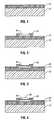
- FIG. 1is an enlarged, cross-sectional view at an early stage of manufacture in accordance with one embodiment of the present invention
- FIG. 2is an enlarged, cross-sectional view at a subsequent state of manufacture in accordance with one embodiment of the present invention
- FIG. 3is an enlarged, cross-sectional view at a subsequent state of manufacture in accordance with one embodiment of the present invention.
- FIG. 4is an enlarged, cross-sectional view at a subsequent stage of manufacture in accordance with one embodiment of the present invention.
- a semiconductor substrate 12may be a semiconductor wafer in one embodiment of the present invention.
- a blanket epitaxial wafermay be used as the substrate 12 .
- the substrate 12may be covered by an insulating layer 14 .
- the layer 14serves to electrically isolate the substrate 12 from an overlying carbon nanotube channel.
- the insulating layer 14may be formed of oxides such as silicon dioxide or metal oxides such as hafnium or lanthanum oxide.
- high dielectric constant materialsmay also be utilized. These materials may have dielectric constants greater than 10.
- the resulting structuremay have characteristics similar to those of silicon over insulator (SOI) substrates.
- the insulating layer 14may act like a buried oxide in SOI technologies in some embodiments.
- the carbon nanotubes 16may then be positioned over the insulating layer 14 .
- the carbon nanotubesmay be deposited from solution, for example, using Langmuir-Blodgett or self-assembly-techniques.
- the carbon nanotubesmay be directly grown on the insulating layer 14 over the substrate 12 .
- the carbon nanotubes 16may be single walled carbon nanotubes.
- the source and drain 18may be formed as metal contacts extending over the carbon nanotubes 16 . They may be formed by depositing a suitable metal layer and using lithography, metallization, and lift-off. By avoiding the use of etching, the carbon nanotubes 16 may be protected from etch chemistries to which they may be susceptible. Suitable metals for the source drain 18 include high workfunction materials (such as platinum) for PMOS transistors and low workfunction materials (such as aluminum) for NMOS transistors.
- a high dielectric constant layer 20may then be deposited, for example, by atomic layer deposition.
- Suitable materials for the layer 20include metal oxides such as hafnium or lanthanum oxide.
- the layer 20may have a thickness of from 10 Angstroms to 5 50 Angstroms in some embodiments.
- a pre-cleanPrior to depositing the layer 20 , a pre-clean may be completed.
- the use of oxidizing agentsmay be avoided in some cases, or severely limited, to reduce burning of the carbon nanotubes 16 .
- deposition temperaturesmay be limited to below 400 degrees C. to avoid adversely affecting the carbon nanotubes 16 .
- a metal gate 22may be deposited and patterned. Temperatures above 400 degrees C. are advantageously avoided. Lithography, metallization, and lift-off techniques may be used again in order to protect the carbon nanotubes 16 in some embodiments. The lack of high temperature processing allows the metal workfunction to be tuned for specific p-channel applications. Suitable materials for p-channel devices include platinum. The thickness of the metal gate 22 may be from 100 to 1000 Angstroms in some embodiments.
- the excellent mobility of carbon nanotube channelsmay be combined with excellent gate coupling, achieved by high dielectric constant layer 20 .
- workfunction engineeringmay be subject to process and performance optimization.
Landscapes
- Engineering & Computer Science (AREA)
- Chemical & Material Sciences (AREA)
- Nanotechnology (AREA)
- Physics & Mathematics (AREA)
- Mathematical Physics (AREA)
- Theoretical Computer Science (AREA)
- Crystallography & Structural Chemistry (AREA)
- Inorganic Chemistry (AREA)
- Thin Film Transistor (AREA)
- Metal-Oxide And Bipolar Metal-Oxide Semiconductor Integrated Circuits (AREA)
Abstract
Description
- This invention relates generally to carbon nanotube transistors.
- Carbon nanotube transistors may be advantageous because carbon nanotubes have excellent electrical properties with both holes and electrons. For example, carbon nanotubes show very high theoretical values for mobility.
- Single walled semiconducting nanotubes, having diameters between 1.5 and 2 nanometers, exhibit energy bandgaps of from 0.65 to 0.4 eV. With top gate carbon nanotube transistors having metal gates and scaled dielectrics (e.g., less than 20 Angstroms), poor electrical characteristics may be exhibited, such as high gate current. In addition, the nucleation of oxides on the carbon nanotubes is poorly understood and poorly controlled.
- Thus, there is a need for better ways to make metal gate carbon nanotube transistors.
FIG. 1 is an enlarged, cross-sectional view at an early stage of manufacture in accordance with one embodiment of the present invention;FIG. 2 is an enlarged, cross-sectional view at a subsequent state of manufacture in accordance with one embodiment of the present invention;FIG. 3 is an enlarged, cross-sectional view at a subsequent state of manufacture in accordance with one embodiment of the present invention; andFIG. 4 is an enlarged, cross-sectional view at a subsequent stage of manufacture in accordance with one embodiment of the present invention.- Referring to
FIG. 1 , asemiconductor substrate 12 may be a semiconductor wafer in one embodiment of the present invention. For example, a blanket epitaxial wafer may be used as thesubstrate 12. Thesubstrate 12 may be covered by aninsulating layer 14. Thelayer 14 serves to electrically isolate thesubstrate 12 from an overlying carbon nanotube channel. For example, theinsulating layer 14 may be formed of oxides such as silicon dioxide or metal oxides such as hafnium or lanthanum oxide. In general, high dielectric constant materials may also be utilized. These materials may have dielectric constants greater than 10. - The resulting structure may have characteristics similar to those of silicon over insulator (SOI) substrates. Particularly, the
insulating layer 14 may act like a buried oxide in SOI technologies in some embodiments. - Referring to
FIG. 2 , thecarbon nanotubes 16 may then be positioned over theinsulating layer 14. The carbon nanotubes may be deposited from solution, for example, using Langmuir-Blodgett or self-assembly-techniques. Alternatively, the carbon nanotubes may be directly grown on theinsulating layer 14 over thesubstrate 12. In some embodiments, thecarbon nanotubes 16 may be single walled carbon nanotubes. - The source and
drain 18 may be formed as metal contacts extending over thecarbon nanotubes 16. They may be formed by depositing a suitable metal layer and using lithography, metallization, and lift-off. By avoiding the use of etching, thecarbon nanotubes 16 may be protected from etch chemistries to which they may be susceptible. Suitable metals for thesource drain 18 include high workfunction materials (such as platinum) for PMOS transistors and low workfunction materials (such as aluminum) for NMOS transistors. - Referring to
FIG. 3 , a high dielectricconstant layer 20 may then be deposited, for example, by atomic layer deposition. Suitable materials for thelayer 20 include metal oxides such as hafnium or lanthanum oxide. Thelayer 20 may have a thickness of from 10 Angstroms to 5 50 Angstroms in some embodiments. - Prior to depositing the
layer 20, a pre-clean may be completed. The use of oxidizing agents may be avoided in some cases, or severely limited, to reduce burning of thecarbon nanotubes 16. In addition, deposition temperatures may be limited to below 400 degrees C. to avoid adversely affecting thecarbon nanotubes 16. - Finally, referring to
FIG. 4 , ametal gate 22 may be deposited and patterned. Temperatures above 400 degrees C. are advantageously avoided. Lithography, metallization, and lift-off techniques may be used again in order to protect thecarbon nanotubes 16 in some embodiments. The lack of high temperature processing allows the metal workfunction to be tuned for specific p-channel applications. Suitable materials for p-channel devices include platinum. The thickness of themetal gate 22 may be from 100 to 1000 Angstroms in some embodiments. - In general, after the
carbon nanotubes 18 are deposited inFIG. 2 , it is advantageous to avoid exposing the structure to temperatures above 400 degrees C. Moreover, it is preferable to limit the processing ambient atmosphere to those atmospheres having an oxygen content of less than 100 ppm. - In some embodiments, the excellent mobility of carbon nanotube channels may be combined with excellent gate coupling, achieved by high dielectric
constant layer 20. In addition, when selecting the gate metal, workfunction engineering may be subject to process and performance optimization. - While the present invention has been described with respect to a limited number of embodiments, those skilled in the art will appreciate numerous modifications and variations therefrom. It is intended that the appended claims cover all such modifications and variations as fall within the true spirit and scope of this present invention.
Claims (20)
1. A method comprising:
forming a layer of carbon nanotubes;
providing an insulating layer over said carbon nanotubes; and
providing a metal gate electrode over said insulating layer.
2. The method ofclaim 1 including forming a transistor at a temperature less than 400 C.
3. The method ofclaim 1 including forming a transistor using environments having an oxygen content less than 100 ppm.
4. The method ofclaim 1 including forming metal contacts over said nanotubes.
5. The method ofclaim 4 including using a lift off technique to form said contacts.
6. The method ofclaim 1 including forming said layer of carbon nanotubes over a substrate including an epitaxial silicon layer covered by oxide.
7. The method ofclaim 1 including forming the insulating layer with a dielectric constant greater than ten.
8. The method ofclaim 1 including forming said insulating layer over a substrate in the form of a blanket epitaxial wafer.
9. An integrated circuit comprising:
a semiconductor substrate;
an insulating layer over said substrate;
a layer of carbon nanotubes over said insulating layer; and
a metal gate electrode over said insulating layer.
10. The circuit ofclaim 9 including a metal source drain over said carbon nanotubes.
11. The circuit ofclaim 9 wherein said substrate includes an epitaxial silicon layer.
12. The circuit ofclaim 9 wherein said insulating layer has a dielectric constant greater than ten.
13. The circuit ofclaim 9 including a PMOS transistor.
14. The circuit ofclaim 9 including an NMOS transistor.
15. The circuit ofclaim 9 wherein said carbon nanotubes are single walled carbon nanotubes.
16. An integrated circuit comprising:
a semiconductor substrate;
an insulating layer over said substrate, said insulating layer having a dielectric constant greater than ten;
a layer of carbon nanotubes over said insulating layer;
a metal gate electrode over said insulating layer; and
a metal source drain over said insulating layer.
17. The circuit ofclaim 16 wherein said substrate includes an epitaxial silicon layer.
18. The circuit ofclaim 16 wherein said circuit includes a PMOS transistor.
19. The circuit ofclaim 16 wherein said circuit includes an NMOS transistor.
20. The circuit ofclaim 16 wherein said carbon nanotubes are single walled carbon nanotubes.
Priority Applications (1)
| Application Number | Priority Date | Filing Date | Title |
|---|---|---|---|
| US11/059,184US20060180859A1 (en) | 2005-02-16 | 2005-02-16 | Metal gate carbon nanotube transistor |
Applications Claiming Priority (1)
| Application Number | Priority Date | Filing Date | Title |
|---|---|---|---|
| US11/059,184US20060180859A1 (en) | 2005-02-16 | 2005-02-16 | Metal gate carbon nanotube transistor |
Publications (1)
| Publication Number | Publication Date |
|---|---|
| US20060180859A1true US20060180859A1 (en) | 2006-08-17 |
Family
ID=36814806
Family Applications (1)
| Application Number | Title | Priority Date | Filing Date |
|---|---|---|---|
| US11/059,184AbandonedUS20060180859A1 (en) | 2005-02-16 | 2005-02-16 | Metal gate carbon nanotube transistor |
Country Status (1)
| Country | Link |
|---|---|
| US (1) | US20060180859A1 (en) |
Cited By (17)
| Publication number | Priority date | Publication date | Assignee | Title |
|---|---|---|---|---|
| US20080121996A1 (en)* | 2004-09-13 | 2008-05-29 | Park Wan-Jun | Transistor with carbon nanotube channel and method of manufacturing the same |
| US20090085198A1 (en)* | 2007-09-30 | 2009-04-02 | Unnikrishnan Vadakkanmaruveedu | Nanotube based vapor chamber for die level cooling |
| US20100301336A1 (en)* | 2009-06-02 | 2010-12-02 | International Business Machines Corporation | Method to Improve Nucleation of Materials on Graphene and Carbon Nanotubes |
| US7898041B2 (en)* | 2005-06-30 | 2011-03-01 | Intel Corporation | Block contact architectures for nanoscale channel transistors |
| US7989280B2 (en) | 2005-11-30 | 2011-08-02 | Intel Corporation | Dielectric interface for group III-V semiconductor device |
| US8071983B2 (en) | 2005-06-21 | 2011-12-06 | Intel Corporation | Semiconductor device structures and methods of forming semiconductor structures |
| US8084818B2 (en) | 2004-06-30 | 2011-12-27 | Intel Corporation | High mobility tri-gate devices and methods of fabrication |
| US20120074387A1 (en)* | 2010-09-23 | 2012-03-29 | Sean King | Microelectronic transistor having an epitaxial graphene channel layer |
| US8183646B2 (en) | 2005-02-23 | 2012-05-22 | Intel Corporation | Field effect transistor with narrow bandgap source and drain regions and method of fabrication |
| US8273626B2 (en) | 2003-06-27 | 2012-09-25 | Intel Corporationn | Nonplanar semiconductor device with partially or fully wrapped around gate electrode and methods of fabrication |
| US8294180B2 (en) | 2005-09-28 | 2012-10-23 | Intel Corporation | CMOS devices with a single work function gate electrode and method of fabrication |
| US8362566B2 (en) | 2008-06-23 | 2013-01-29 | Intel Corporation | Stress in trigate devices using complimentary gate fill materials |
| US8502351B2 (en) | 2004-10-25 | 2013-08-06 | Intel Corporation | Nonplanar device with thinned lower body portion and method of fabrication |
| US8617945B2 (en) | 2006-08-02 | 2013-12-31 | Intel Corporation | Stacking fault and twin blocking barrier for integrating III-V on Si |
| US9337307B2 (en) | 2005-06-15 | 2016-05-10 | Intel Corporation | Method for fabricating transistor with thinned channel |
| CN110364438A (en)* | 2019-05-29 | 2019-10-22 | 北京华碳元芯电子科技有限责任公司 | Transistor and its manufacturing method |
| US20230070355A1 (en)* | 2021-09-08 | 2023-03-09 | Samsung Electronics Co., Ltd. | Layer structure including metal layer and carbon layer, method of manufacturing the layer structure, electronic device including the layer structure, and electronic apparatus including the electronic device |
Citations (4)
| Publication number | Priority date | Publication date | Assignee | Title |
|---|---|---|---|---|
| US6548313B1 (en)* | 2002-05-31 | 2003-04-15 | Intel Corporation | Amorphous carbon insulation and carbon nanotube wires |
| US20030178617A1 (en)* | 2002-03-20 | 2003-09-25 | International Business Machines Corporation | Self-aligned nanotube field effect transistor and method of fabricating same |
| US6762237B2 (en)* | 2001-06-08 | 2004-07-13 | Eikos, Inc. | Nanocomposite dielectrics |
| US20050212014A1 (en)* | 2004-03-26 | 2005-09-29 | Masahiro Horibe | Semiconductor device and semiconductor sensor |
- 2005
- 2005-02-16USUS11/059,184patent/US20060180859A1/ennot_activeAbandoned
Patent Citations (4)
| Publication number | Priority date | Publication date | Assignee | Title |
|---|---|---|---|---|
| US6762237B2 (en)* | 2001-06-08 | 2004-07-13 | Eikos, Inc. | Nanocomposite dielectrics |
| US20030178617A1 (en)* | 2002-03-20 | 2003-09-25 | International Business Machines Corporation | Self-aligned nanotube field effect transistor and method of fabricating same |
| US6548313B1 (en)* | 2002-05-31 | 2003-04-15 | Intel Corporation | Amorphous carbon insulation and carbon nanotube wires |
| US20050212014A1 (en)* | 2004-03-26 | 2005-09-29 | Masahiro Horibe | Semiconductor device and semiconductor sensor |
Cited By (45)
| Publication number | Priority date | Publication date | Assignee | Title |
|---|---|---|---|---|
| US8273626B2 (en) | 2003-06-27 | 2012-09-25 | Intel Corporationn | Nonplanar semiconductor device with partially or fully wrapped around gate electrode and methods of fabrication |
| US8084818B2 (en) | 2004-06-30 | 2011-12-27 | Intel Corporation | High mobility tri-gate devices and methods of fabrication |
| US20080121996A1 (en)* | 2004-09-13 | 2008-05-29 | Park Wan-Jun | Transistor with carbon nanotube channel and method of manufacturing the same |
| US9190518B2 (en) | 2004-10-25 | 2015-11-17 | Intel Corporation | Nonplanar device with thinned lower body portion and method of fabrication |
| US10236356B2 (en) | 2004-10-25 | 2019-03-19 | Intel Corporation | Nonplanar device with thinned lower body portion and method of fabrication |
| US8749026B2 (en) | 2004-10-25 | 2014-06-10 | Intel Corporation | Nonplanar device with thinned lower body portion and method of fabrication |
| US9741809B2 (en) | 2004-10-25 | 2017-08-22 | Intel Corporation | Nonplanar device with thinned lower body portion and method of fabrication |
| US8502351B2 (en) | 2004-10-25 | 2013-08-06 | Intel Corporation | Nonplanar device with thinned lower body portion and method of fabrication |
| US8664694B2 (en) | 2005-02-23 | 2014-03-04 | Intel Corporation | Field effect transistor with narrow bandgap source and drain regions and method of fabrication |
| US9614083B2 (en) | 2005-02-23 | 2017-04-04 | Intel Corporation | Field effect transistor with narrow bandgap source and drain regions and method of fabrication |
| US8816394B2 (en) | 2005-02-23 | 2014-08-26 | Intel Corporation | Field effect transistor with narrow bandgap source and drain regions and method of fabrication |
| US9368583B2 (en) | 2005-02-23 | 2016-06-14 | Intel Corporation | Field effect transistor with narrow bandgap source and drain regions and method of fabrication |
| US9748391B2 (en) | 2005-02-23 | 2017-08-29 | Intel Corporation | Field effect transistor with narrow bandgap source and drain regions and method of fabrication |
| US8368135B2 (en) | 2005-02-23 | 2013-02-05 | Intel Corporation | Field effect transistor with narrow bandgap source and drain regions and method of fabrication |
| US9048314B2 (en) | 2005-02-23 | 2015-06-02 | Intel Corporation | Field effect transistor with narrow bandgap source and drain regions and method of fabrication |
| US8183646B2 (en) | 2005-02-23 | 2012-05-22 | Intel Corporation | Field effect transistor with narrow bandgap source and drain regions and method of fabrication |
| US10121897B2 (en) | 2005-02-23 | 2018-11-06 | Intel Corporation | Field effect transistor with narrow bandgap source and drain regions and method of fabrication |
| US9806195B2 (en) | 2005-06-15 | 2017-10-31 | Intel Corporation | Method for fabricating transistor with thinned channel |
| US9337307B2 (en) | 2005-06-15 | 2016-05-10 | Intel Corporation | Method for fabricating transistor with thinned channel |
| US11978799B2 (en) | 2005-06-15 | 2024-05-07 | Tahoe Research, Ltd. | Method for fabricating transistor with thinned channel |
| US8581258B2 (en) | 2005-06-21 | 2013-11-12 | Intel Corporation | Semiconductor device structures and methods of forming semiconductor structures |
| US9385180B2 (en) | 2005-06-21 | 2016-07-05 | Intel Corporation | Semiconductor device structures and methods of forming semiconductor structures |
| US8071983B2 (en) | 2005-06-21 | 2011-12-06 | Intel Corporation | Semiconductor device structures and methods of forming semiconductor structures |
| US9761724B2 (en) | 2005-06-21 | 2017-09-12 | Intel Corporation | Semiconductor device structures and methods of forming semiconductor structures |
| US8933458B2 (en) | 2005-06-21 | 2015-01-13 | Intel Corporation | Semiconductor device structures and methods of forming semiconductor structures |
| US7898041B2 (en)* | 2005-06-30 | 2011-03-01 | Intel Corporation | Block contact architectures for nanoscale channel transistors |
| US8294180B2 (en) | 2005-09-28 | 2012-10-23 | Intel Corporation | CMOS devices with a single work function gate electrode and method of fabrication |
| US7989280B2 (en) | 2005-11-30 | 2011-08-02 | Intel Corporation | Dielectric interface for group III-V semiconductor device |
| US8617945B2 (en) | 2006-08-02 | 2013-12-31 | Intel Corporation | Stacking fault and twin blocking barrier for integrating III-V on Si |
| US8623705B2 (en) | 2007-09-30 | 2014-01-07 | Intel Corporation | Nanotube based vapor chamber for die level cooling |
| US20090085198A1 (en)* | 2007-09-30 | 2009-04-02 | Unnikrishnan Vadakkanmaruveedu | Nanotube based vapor chamber for die level cooling |
| US7911052B2 (en) | 2007-09-30 | 2011-03-22 | Intel Corporation | Nanotube based vapor chamber for die level cooling |
| US9806193B2 (en) | 2008-06-23 | 2017-10-31 | Intel Corporation | Stress in trigate devices using complimentary gate fill materials |
| US9450092B2 (en) | 2008-06-23 | 2016-09-20 | Intel Corporation | Stress in trigate devices using complimentary gate fill materials |
| US8741733B2 (en) | 2008-06-23 | 2014-06-03 | Intel Corporation | Stress in trigate devices using complimentary gate fill materials |
| US8362566B2 (en) | 2008-06-23 | 2013-01-29 | Intel Corporation | Stress in trigate devices using complimentary gate fill materials |
| US9224754B2 (en) | 2008-06-23 | 2015-12-29 | Intel Corporation | Stress in trigate devices using complimentary gate fill materials |
| US8816333B2 (en) | 2009-06-02 | 2014-08-26 | International Business Machines Corporation | Method to improve nucleation of materials on graphene and carbon nanotubes |
| TWI481738B (en)* | 2009-06-02 | 2015-04-21 | Ibm | Method for improving nucleation of materials on graphene and carbon nanotubes |
| US20100301336A1 (en)* | 2009-06-02 | 2010-12-02 | International Business Machines Corporation | Method to Improve Nucleation of Materials on Graphene and Carbon Nanotubes |
| US8895352B2 (en)* | 2009-06-02 | 2014-11-25 | International Business Machines Corporation | Method to improve nucleation of materials on graphene and carbon nanotubes |
| US8785261B2 (en)* | 2010-09-23 | 2014-07-22 | Intel Corporation | Microelectronic transistor having an epitaxial graphene channel layer |
| US20120074387A1 (en)* | 2010-09-23 | 2012-03-29 | Sean King | Microelectronic transistor having an epitaxial graphene channel layer |
| CN110364438A (en)* | 2019-05-29 | 2019-10-22 | 北京华碳元芯电子科技有限责任公司 | Transistor and its manufacturing method |
| US20230070355A1 (en)* | 2021-09-08 | 2023-03-09 | Samsung Electronics Co., Ltd. | Layer structure including metal layer and carbon layer, method of manufacturing the layer structure, electronic device including the layer structure, and electronic apparatus including the electronic device |
Similar Documents
| Publication | Publication Date | Title |
|---|---|---|
| US20060180859A1 (en) | Metal gate carbon nanotube transistor | |
| US7955917B2 (en) | Fabrication of self-aligned gallium arsenide MOSFETS using damascene gate methods | |
| US7504336B2 (en) | Methods for forming CMOS devices with intrinsically stressed metal silicide layers | |
| US9805949B2 (en) | High κ gate stack on III-V compound semiconductors | |
| US8101474B2 (en) | Structure and method of forming buried-channel graphene field effect device | |
| US9318573B2 (en) | Field effect transistor having germanium nanorod and method of manufacturing the same | |
| US20090163005A1 (en) | Schottky barrier source/drain N-MOSFET using ytterbium silicide | |
| US10381586B2 (en) | Carbon nanotube field-effect transistor with sidewall-protected metal contacts | |
| Liu et al. | Vertical Ge gate-all-around nanowire pMOSFETs with a diameter down to 20 nm | |
| US8815669B2 (en) | Metal gate structures for CMOS transistor devices having reduced parasitic capacitance | |
| US8658461B2 (en) | Self aligned carbide source/drain FET | |
| JP2004319952A (en) | Semiconductor device and method of manufacturing the same | |
| CN113644110B (en) | Transistor and preparation method thereof | |
| US7880241B2 (en) | Low-temperature electrically activated gate electrode and method of fabricating same | |
| US10396300B2 (en) | Carbon nanotube device with N-type end-bonded metal contacts | |
| US7087476B2 (en) | Using different gate dielectrics with NMOS and PMOS transistors of a complementary metal oxide semiconductor integrated circuit | |
| US20090325370A1 (en) | Field-effect transistor structure and fabrication method thereof | |
| KR100666933B1 (en) | Manufacturing Method of Semiconductor Device | |
| JP4538636B2 (en) | Field effect transistor and manufacturing method thereof | |
| US8518766B2 (en) | Method of forming switching device having a molybdenum oxynitride metal gate | |
| WO2021227344A1 (en) | Transistor and method for fabricating the same | |
| CN113690300A (en) | Transistor with local bottom gate and manufacturing method thereof | |
| US20080290414A1 (en) | Integrating strain engineering to maximize system-on-a-chip performance |
Legal Events
| Date | Code | Title | Description |
|---|---|---|---|
| AS | Assignment | Owner name:INTEL CORPORATION, CALIFORNIA Free format text:ASSIGNMENT OF ASSIGNORS INTEREST;ASSIGNORS:RADOSAVLJEVIC, MARKO;MAJUMDAR, AMLAN;DATTA, SUMAN;AND OTHERS;REEL/FRAME:016289/0593;SIGNING DATES FROM 20040214 TO 20050215 | |
| STCB | Information on status: application discontinuation | Free format text:ABANDONED -- FAILURE TO RESPOND TO AN OFFICE ACTION |