US20060176645A1 - Atomic layer deposition of Dy doped HfO2 films as gate dielectrics - Google Patents
Atomic layer deposition of Dy doped HfO2 films as gate dielectricsDownload PDFInfo
- Publication number
- US20060176645A1 US20060176645A1US11/053,577US5357705AUS2006176645A1US 20060176645 A1US20060176645 A1US 20060176645A1US 5357705 AUS5357705 AUS 5357705AUS 2006176645 A1US2006176645 A1US 2006176645A1
- Authority
- US
- United States
- Prior art keywords
- dielectric
- layer
- forming
- dielectric layer
- precursor
- Prior art date
- Legal status (The legal status is an assumption and is not a legal conclusion. Google has not performed a legal analysis and makes no representation as to the accuracy of the status listed.)
- Granted
Links
Images


Classifications
- H—ELECTRICITY
- H01—ELECTRIC ELEMENTS
- H01L—SEMICONDUCTOR DEVICES NOT COVERED BY CLASS H10
- H01L21/00—Processes or apparatus adapted for the manufacture or treatment of semiconductor or solid state devices or of parts thereof
- H01L21/02—Manufacture or treatment of semiconductor devices or of parts thereof
- H01L21/02104—Forming layers
- H01L21/02107—Forming insulating materials on a substrate
- H01L21/02109—Forming insulating materials on a substrate characterised by the type of layer, e.g. type of material, porous/non-porous, pre-cursors, mixtures or laminates
- H01L21/02112—Forming insulating materials on a substrate characterised by the type of layer, e.g. type of material, porous/non-porous, pre-cursors, mixtures or laminates characterised by the material of the layer
- H01L21/02172—Forming insulating materials on a substrate characterised by the type of layer, e.g. type of material, porous/non-porous, pre-cursors, mixtures or laminates characterised by the material of the layer the material containing at least one metal element, e.g. metal oxides, metal nitrides, metal oxynitrides or metal carbides
- H01L21/02175—Forming insulating materials on a substrate characterised by the type of layer, e.g. type of material, porous/non-porous, pre-cursors, mixtures or laminates characterised by the material of the layer the material containing at least one metal element, e.g. metal oxides, metal nitrides, metal oxynitrides or metal carbides characterised by the metal
- H01L21/02181—Forming insulating materials on a substrate characterised by the type of layer, e.g. type of material, porous/non-porous, pre-cursors, mixtures or laminates characterised by the material of the layer the material containing at least one metal element, e.g. metal oxides, metal nitrides, metal oxynitrides or metal carbides characterised by the metal the material containing hafnium, e.g. HfO2
- C—CHEMISTRY; METALLURGY
- C23—COATING METALLIC MATERIAL; COATING MATERIAL WITH METALLIC MATERIAL; CHEMICAL SURFACE TREATMENT; DIFFUSION TREATMENT OF METALLIC MATERIAL; COATING BY VACUUM EVAPORATION, BY SPUTTERING, BY ION IMPLANTATION OR BY CHEMICAL VAPOUR DEPOSITION, IN GENERAL; INHIBITING CORROSION OF METALLIC MATERIAL OR INCRUSTATION IN GENERAL
- C23C—COATING METALLIC MATERIAL; COATING MATERIAL WITH METALLIC MATERIAL; SURFACE TREATMENT OF METALLIC MATERIAL BY DIFFUSION INTO THE SURFACE, BY CHEMICAL CONVERSION OR SUBSTITUTION; COATING BY VACUUM EVAPORATION, BY SPUTTERING, BY ION IMPLANTATION OR BY CHEMICAL VAPOUR DEPOSITION, IN GENERAL
- C23C16/00—Chemical coating by decomposition of gaseous compounds, without leaving reaction products of surface material in the coating, i.e. chemical vapour deposition [CVD] processes
- C23C16/22—Chemical coating by decomposition of gaseous compounds, without leaving reaction products of surface material in the coating, i.e. chemical vapour deposition [CVD] processes characterised by the deposition of inorganic material, other than metallic material
- C23C16/30—Deposition of compounds, mixtures or solid solutions, e.g. borides, carbides, nitrides
- C23C16/40—Oxides
- C23C16/405—Oxides of refractory metals or yttrium
- C—CHEMISTRY; METALLURGY
- C23—COATING METALLIC MATERIAL; COATING MATERIAL WITH METALLIC MATERIAL; CHEMICAL SURFACE TREATMENT; DIFFUSION TREATMENT OF METALLIC MATERIAL; COATING BY VACUUM EVAPORATION, BY SPUTTERING, BY ION IMPLANTATION OR BY CHEMICAL VAPOUR DEPOSITION, IN GENERAL; INHIBITING CORROSION OF METALLIC MATERIAL OR INCRUSTATION IN GENERAL
- C23C—COATING METALLIC MATERIAL; COATING MATERIAL WITH METALLIC MATERIAL; SURFACE TREATMENT OF METALLIC MATERIAL BY DIFFUSION INTO THE SURFACE, BY CHEMICAL CONVERSION OR SUBSTITUTION; COATING BY VACUUM EVAPORATION, BY SPUTTERING, BY ION IMPLANTATION OR BY CHEMICAL VAPOUR DEPOSITION, IN GENERAL
- C23C16/00—Chemical coating by decomposition of gaseous compounds, without leaving reaction products of surface material in the coating, i.e. chemical vapour deposition [CVD] processes
- C23C16/44—Chemical coating by decomposition of gaseous compounds, without leaving reaction products of surface material in the coating, i.e. chemical vapour deposition [CVD] processes characterised by the method of coating
- C23C16/455—Chemical coating by decomposition of gaseous compounds, without leaving reaction products of surface material in the coating, i.e. chemical vapour deposition [CVD] processes characterised by the method of coating characterised by the method used for introducing gases into reaction chamber or for modifying gas flows in reaction chamber
- C23C16/45523—Pulsed gas flow or change of composition over time
- C23C16/45525—Atomic layer deposition [ALD]
- C23C16/45527—Atomic layer deposition [ALD] characterized by the ALD cycle, e.g. different flows or temperatures during half-reactions, unusual pulsing sequence, use of precursor mixtures or auxiliary reactants or activations
- C23C16/45529—Atomic layer deposition [ALD] characterized by the ALD cycle, e.g. different flows or temperatures during half-reactions, unusual pulsing sequence, use of precursor mixtures or auxiliary reactants or activations specially adapted for making a layer stack of alternating different compositions or gradient compositions
- H—ELECTRICITY
- H01—ELECTRIC ELEMENTS
- H01L—SEMICONDUCTOR DEVICES NOT COVERED BY CLASS H10
- H01L21/00—Processes or apparatus adapted for the manufacture or treatment of semiconductor or solid state devices or of parts thereof
- H01L21/02—Manufacture or treatment of semiconductor devices or of parts thereof
- H01L21/02104—Forming layers
- H01L21/02107—Forming insulating materials on a substrate
- H01L21/02109—Forming insulating materials on a substrate characterised by the type of layer, e.g. type of material, porous/non-porous, pre-cursors, mixtures or laminates
- H01L21/022—Forming insulating materials on a substrate characterised by the type of layer, e.g. type of material, porous/non-porous, pre-cursors, mixtures or laminates the layer being a laminate, i.e. composed of sublayers, e.g. stacks of alternating high-k metal oxides
- H—ELECTRICITY
- H01—ELECTRIC ELEMENTS
- H01L—SEMICONDUCTOR DEVICES NOT COVERED BY CLASS H10
- H01L21/00—Processes or apparatus adapted for the manufacture or treatment of semiconductor or solid state devices or of parts thereof
- H01L21/02—Manufacture or treatment of semiconductor devices or of parts thereof
- H01L21/04—Manufacture or treatment of semiconductor devices or of parts thereof the devices having potential barriers, e.g. a PN junction, depletion layer or carrier concentration layer
- H01L21/18—Manufacture or treatment of semiconductor devices or of parts thereof the devices having potential barriers, e.g. a PN junction, depletion layer or carrier concentration layer the devices having semiconductor bodies comprising elements of Group IV of the Periodic Table or AIIIBV compounds with or without impurities, e.g. doping materials
- H01L21/28—Manufacture of electrodes on semiconductor bodies using processes or apparatus not provided for in groups H01L21/20 - H01L21/268
- H01L21/28008—Making conductor-insulator-semiconductor electrodes
- H01L21/28017—Making conductor-insulator-semiconductor electrodes the insulator being formed after the semiconductor body, the semiconductor being silicon
- H01L21/28158—Making the insulator
- H01L21/28167—Making the insulator on single crystalline silicon, e.g. using a liquid, i.e. chemical oxidation
- H01L21/28194—Making the insulator on single crystalline silicon, e.g. using a liquid, i.e. chemical oxidation by deposition, e.g. evaporation, ALD, CVD, sputtering, laser deposition
- H—ELECTRICITY
- H10—SEMICONDUCTOR DEVICES; ELECTRIC SOLID-STATE DEVICES NOT OTHERWISE PROVIDED FOR
- H10D—INORGANIC ELECTRIC SEMICONDUCTOR DEVICES
- H10D30/00—Field-effect transistors [FET]
- H10D30/60—Insulated-gate field-effect transistors [IGFET]
- H—ELECTRICITY
- H10—SEMICONDUCTOR DEVICES; ELECTRIC SOLID-STATE DEVICES NOT OTHERWISE PROVIDED FOR
- H10D—INORGANIC ELECTRIC SEMICONDUCTOR DEVICES
- H10D64/00—Electrodes of devices having potential barriers
- H10D64/60—Electrodes characterised by their materials
- H10D64/66—Electrodes having a conductor capacitively coupled to a semiconductor by an insulator, e.g. MIS electrodes
- H10D64/68—Electrodes having a conductor capacitively coupled to a semiconductor by an insulator, e.g. MIS electrodes characterised by the insulator, e.g. by the gate insulator
- H10D64/681—Electrodes having a conductor capacitively coupled to a semiconductor by an insulator, e.g. MIS electrodes characterised by the insulator, e.g. by the gate insulator having a compositional variation, e.g. multilayered
- H10D64/685—Electrodes having a conductor capacitively coupled to a semiconductor by an insulator, e.g. MIS electrodes characterised by the insulator, e.g. by the gate insulator having a compositional variation, e.g. multilayered being perpendicular to the channel plane
- H—ELECTRICITY
- H10—SEMICONDUCTOR DEVICES; ELECTRIC SOLID-STATE DEVICES NOT OTHERWISE PROVIDED FOR
- H10D—INORGANIC ELECTRIC SEMICONDUCTOR DEVICES
- H10D64/00—Electrodes of devices having potential barriers
- H10D64/60—Electrodes characterised by their materials
- H10D64/66—Electrodes having a conductor capacitively coupled to a semiconductor by an insulator, e.g. MIS electrodes
- H10D64/68—Electrodes having a conductor capacitively coupled to a semiconductor by an insulator, e.g. MIS electrodes characterised by the insulator, e.g. by the gate insulator
- H10D64/691—Electrodes having a conductor capacitively coupled to a semiconductor by an insulator, e.g. MIS electrodes characterised by the insulator, e.g. by the gate insulator comprising metallic compounds, e.g. metal oxides or metal silicates
- H—ELECTRICITY
- H01—ELECTRIC ELEMENTS
- H01L—SEMICONDUCTOR DEVICES NOT COVERED BY CLASS H10
- H01L21/00—Processes or apparatus adapted for the manufacture or treatment of semiconductor or solid state devices or of parts thereof
- H01L21/02—Manufacture or treatment of semiconductor devices or of parts thereof
- H01L21/02104—Forming layers
- H01L21/02107—Forming insulating materials on a substrate
- H01L21/02225—Forming insulating materials on a substrate characterised by the process for the formation of the insulating layer
- H01L21/0226—Forming insulating materials on a substrate characterised by the process for the formation of the insulating layer formation by a deposition process
- H01L21/02263—Forming insulating materials on a substrate characterised by the process for the formation of the insulating layer formation by a deposition process deposition from the gas or vapour phase
- H01L21/02271—Forming insulating materials on a substrate characterised by the process for the formation of the insulating layer formation by a deposition process deposition from the gas or vapour phase deposition by decomposition or reaction of gaseous or vapour phase compounds, i.e. chemical vapour deposition
- H01L21/0228—Forming insulating materials on a substrate characterised by the process for the formation of the insulating layer formation by a deposition process deposition from the gas or vapour phase deposition by decomposition or reaction of gaseous or vapour phase compounds, i.e. chemical vapour deposition deposition by cyclic CVD, e.g. ALD, ALE, pulsed CVD
Definitions
- This applicationrelates generally to semiconductor devices and device fabrication and, more particularly, to dielectric layers and their method of fabrication.
- the semiconductor device industryhas a market driven need to reduce the size of devices such as transistors.
- the thickness of the silicon dioxide, SiO 2 , gate dielectricis reduced in proportion to the shrinkage of the gate length.
- MOSFETmetal-oxide-semiconductor field effect transistor
- Such scaling of gate dielectricsmay be the most difficult issue facing the production of the next generation of MOSFETs.
- the increasingly small and reliable integrated circuits (ICs)will likely be used in products such as processor chips, mobile telephones, and memory devices such as dynamic random access memories (DRAMs).
- This device scalingincludes scaling the gate dielectric, which has primarily been formed of silicon dioxide (SiO 2 ).
- SiO 2silicon dioxide
- a thermally grown amorphous SiO 2 layerprovides an electrically and thermodynamically stable material, where the interface of the SiO 2 layer with underlying silicon provides a high quality interface as well as superior electrical isolation properties.
- increased scaling and other requirements in microelectronic deviceshave created problems as the gate dielectric has become thinner, and generated the need to use other dielectric materials as gate dielectrics, in particular dielectric materials with higher dielectric constants (k).
- An embodiment for a method for forming an electronic deviceincludes forming a dielectric layer by using an atomic layer deposition (ALD) technique to form a dielectric having dysprosium oxide (for example Dy 2 O 3 ) doped hafnium oxide (for example HfO 2 ).
- An embodimentincludes forming an integrated circuit having a dielectric layer made by using an atomic layer deposition to form dysprosium oxide doped hafnium oxide, and having a conductive layer on the dielectric layer.
- Another embodimentincludes a method of forming a memory array having an atomic layer deposited dielectric layer of dysprosium oxide doped hafnium oxide, contacting a conductive layer and forming an address decoder coupled to the memory array.
- Embodimentsinclude structures for capacitors, transistors, memory devices, and electronic systems with dielectric layers containing an atomic layer deposited dysprosium doped hafnium oxide dielectric, and methods for forming such structures.
- FIG. 1depicts an atomic layer deposition system for fabricating a dielectric layer formed as a nanolaminate layered sequence of dysprosium oxide and hafnium oxide, according to various embodiments;
- FIG. 2illustrates a flow diagram of elements for an embodiment of a method to form a dielectric layer containing dysprosium doped hafnium oxide by atomic layer deposition according to various embodiments;
- FIG. 3illustrates an embodiment of a configuration of a transistor having a dielectric layer containing an atomic layer deposited dielectric layer containing dysprosium doped hafnium oxide;
- FIG. 4shows an embodiment of a configuration of a capacitor having a dielectric layer containing an atomic layer deposited dysprosium doped hafnium oxide
- FIG. 5is a simplified diagram for an embodiment of a controller coupled to an electronic device.
- FIG. 6illustrates a diagram for an embodiment of an electronic system having devices with a dielectric film containing an atomic layer deposited nanolaminate layered sequence of praseodymium oxide and zirconium oxide dielectric layer.
- wafer and substrate used in the following descriptioninclude any structure having an exposed surface with which to form an integrated circuit (IC) structure.
- substrateis understood to include semiconductor wafers.
- substrateis also used to refer to semiconductor structures during processing, and may include other layers that have been fabricated thereupon. Both wafer and substrate include doped and undoped semiconductors, epitaxial semiconductor layers supported by a base semiconductor or insulator, as well as other semiconductor structures well known to one skilled in the art.
- conductoris understood to generally include n-type and p-type semiconductors and the term insulator or dielectric is defined to include any material that is less electrically conductive than the materials referred to as conductors or as semiconductors.
- horizontalas used in this application is defined as a plane parallel to the conventional plane or surface of a wafer or substrate, regardless of the orientation of the wafer or substrate.
- verticalrefers to a direction perpendicular to the horizontal as defined above. Prepositions, such as “on”, “side” (as in “sidewall”), “higher”, “lower”, “over” and “under” are defined with respect to the conventional plane or surface being on the top surface of the wafer or substrate, regardless of the orientation of the wafer or substrate.
- Dysprosiumis elemental metal number 66 and is part of the lanthanide series of elements.
- Hafniumis elemental metal number 72 , and is situated next to tantalum and right after the lanthanide metals on the periodic table of elements.
- Hafnium oxide filmscan be atomic layer deposited using various precursors such as hafnium tetraiodide and oxygen at a temperature of between 400 to 700 degrees C., or hafnium tetrachloride and steam at 300 degrees C., or anhydrous hafnium nitride (Hf(NO 3 ) 4 ) and ozone at 160 degrees C.
- Dysprosium oxide filmscan be atomic layer deposited using various precursors such as volatile diketonate chelates (for example 2,2,6,6-tetramethyl-3,5-heptanedione) and ozone at 300 degrees C. Each of these films may have a very tightly controlled thickness for each deposition cycle that depends on the saturation of the substrate surface. For example the hafnium oxide layers may be typically 0.14 nm thick per deposition cycle. If repetitive layers of hafnium oxide are grown upon one another, then the single resulting film of hafnium oxide will have a thickness that is easily controlled by simply controlling the number of deposition cycles run. The surface of the ALD formed is also very smooth and continuous, even over sharp underlying topography.
- the deposition cyclesmay also be alternated between the two different oxides and the resulting film may either be a nanolaminate of the two, or more, different oxides, or the oxides may form an alloy with each other if the similarity between the two metals results in miscible materials.
- the film propertiesmay vary depending upon the ratio of the two or more different materials, and thus materials may be formed that have engineered properties. For example, to form a 10% dysprosium alloy with hafnium oxide, deposit nine layers of hafnium oxide and then one layer of dysprosium oxide and repeat until the desired thickness is achieved.
- the dielectric structureis formed by depositing hafnium by atomic layer deposition onto a substrate surface using precursor chemicals to form a film of HfO 2 , followed by ALD depositing dysprosium onto the substrate using precursor chemicals to form Dy 2 O 3 , and repeating as often as necessary to form a dielectric structure of the required thickness.
- An alloyed dielectric layer of dysprosium oxide and hafnium oxidemay be beneficially used because the relatively high dielectric constant (high-k) of 10-12 of the film, as compared to 3.9 for silicon dioxide, and the excellent current leakage value, provides the functionality of a much thinner silicon dioxide film without the reliability loss consequent to using such physically thin films.
- a gate dielectric in a transistorhas both a physical gate dielectric thickness and an equivalent oxide thickness (t eq ).
- the equivalent oxide thicknessquantifies the electrical properties, such as capacitance, of the gate dielectric in terms of a representative physical thickness.
- t eqis defined as the thickness of a theoretical SiO 2 layer that would be required to have the same capacitance density as a given dielectric, ignoring leakage current and reliability considerations.
- a SiO 2 layer of thickness, t, deposited on a Si surface as a gate dielectricwill have a t eq larger than its thickness, t.
- This t eqresults from the capacitance in the surface channel on which the SiO 2 is deposited due to the formation of a depletion/inversion region.
- This depletion/inversion regioncan result in t eq being from 3 to 6 Angstroms ( ⁇ ) larger than the SiO 2 thickness, t.
- the gate dielectric equivalent oxide thicknessto under 10 ⁇
- the physical thickness requirement for a SiO 2 layer used for a gate dielectricwould be need to be approximately 4 to 7 ⁇ .
- SiO 2 layerAdditional requirements on a SiO 2 layer would depend on the gate electrode used in conjunction with the SiO 2 gate dielectric. Using a conventional polysilicon gate would result in an additional increase in t eq for the SiO 2 layer. This additional thickness could be eliminated by using a metal gate electrode, though metal gates are not currently used in typical complementary metal-oxide-semiconductor field effect transistor (CMOS) technology. Thus, future devices would be designed towards a physical SiO 2 gate dielectric layer of about 5 ⁇ or less.
- CMOScomplementary metal-oxide-semiconductor field effect transistor
- Silicon dioxideis used as a gate dielectric, in part, due to its electrical isolation properties in a SiO 2 —Si based structure. This electrical isolation is due to the relatively large band gap of SiO 2 (8.9 eV), which makes it a good insulator. Significant reductions in its band gap would eliminate it as a material for use as a gate dielectric.
- the thickness of a SiO 2 layerdecreases, the number of atomic layers, or monolayers of the material in the thickness decreases. At a certain thickness, the number of monolayers will be sufficiently small that the SiO 2 layer will not have a complete arrangement of atoms as in a thicker or bulk layer.
- a thin SiO 2 layer of only one or two monolayerswill not form a full band gap.
- the lack of a full band gap in a SiO 2 gate dielectricmay cause an effective short between an underlying conductive silicon channel and an overlying polysilicon gate. This undesirable property sets a limit on the physical thickness to which a SiO 2 layer can be scaled. The minimum thickness due to this monolayer effect is thought to be about 7-8 ⁇ . Therefore, for future devices to have a t eq less than about 10 ⁇ , other dielectrics than SiO 2 need to be considered for use as a gate dielectric.
- materials with a dielectric constant greater than that of SiO 2will have a physical thickness that can be considerably larger than a desired t eq , while providing the desired equivalent oxide thickness.
- an alternate dielectric material with a dielectric constant of 10could have a thickness of about 25.6 ⁇ to provide a t eq of 10 ⁇ , not including any depletion/inversion layer effects.
- a reduced equivalent oxide thickness for transistorscan be realized by using dielectric materials with higher dielectric constants than SiO 2 .
- the thinner equivalent oxide thickness required for lower transistor operating voltages and smaller transistor dimensionsmay be realized by a significant number of materials, but additional fabricating requirements makes determining a suitable replacement for SiO 2 difficult.
- the current view for the future of the microelectronics industrystill predicts silicon based devices. This requires that the gate dielectric employed be grown on a silicon substrate or silicon layer, which places significant constraints on the substitute dielectric material. During the formation of the dielectric on the silicon layer, there exists the possibility that a small layer of SiO 2 could be formed in addition to the desired dielectric. The result would effectively be a dielectric layer consisting of two sub-layers in parallel with each other and the silicon layer on which the dielectric is formed.
- the resulting capacitancewould be that of two dielectrics in series.
- the t eqt SiO 2 +( ⁇ ox / ⁇ ) t.
- SiO 2As a gate dielectric, One of the advantages of using SiO 2 as a gate dielectric has been that the formation of the SiO 2 layer results in an amorphous gate dielectric. Having an amorphous structure for a gate dielectric provides reduced leakage current problems associated with grain boundaries in polycrystalline gate dielectrics, which may cause high leakage paths. Additionally, grain size and orientation changes throughout a polycrystalline gate dielectric can cause variations in the film's dielectric constant, along with uniformity and surface topography problems. Typically, materials having the advantage of a high dielectric constant relative to SiO 2 also have the disadvantage of a crystalline form, at least in a bulk configuration. The best candidates for replacing SiO 2 as a gate dielectric are those with high dielectric constant, which can be fabricated as a thin layer with an amorphous form.
- High- ⁇ dielectric materialsinclude materials having a dielectric constant greater than silicon dioxide, for example, dielectric materials having a dielectric constant greater than about twice the dielectric constant of silicon dioxide.
- An appropriate high- ⁇ gate dielectricshould have a large energy gap (E g ) and large energy barrier heights with the silicon substrate for both electrons and holes.
- the band gapis inversely related to the dielectric constant for a high-K material, which lessens some advantages of the high- ⁇ material.
- a set of high- ⁇ dielectric candidates for replacing silicon oxide as the dielectric material in electronic components in integrated circuitincludes the lanthanide oxides such as Pr 2 O 3 , La 2 O 3 , Nd 2 O 3 , Sm 2 O 3 , Gd 2 O 3 , Dy 2 O 3 , Ce 2 O 3 , Tb 2 O 3 , Er 2 O 3 , Eu 2 O 3 , Lu 2 O 3 , Tm 2 O 3 , Ho 2 O 3 , Pm 2 O 3 , and Yb 2 O 3 .
- the lanthanide oxidessuch as Pr 2 O 3 , La 2 O 3 , Nd 2 O 3 , Sm 2 O 3 , Gd 2 O 3 , Dy 2 O 3 , Ce 2 O 3 , Tb 2 O 3 , Er 2 O 3 , Eu 2 O 3 , Lu 2 O 3 , Tm 2 O 3 , Ho 2 O 3 , Pm 2 O 3 , and Yb 2 O 3 .
- lanthanide silicateszirconium oxide ZrO 2 , and hafnium oxide HfO 2 , which as previously noted is element number 72 , and the first element after the end of the lanthanide series of the periodic table of elements.
- Such high dielectric constant layersprovide a significantly thinner equivalent oxide thickness compared with a silicon oxide layer having the same physical thickness. Alternately, such dielectric layers provide a significantly thicker physical thickness than a silicon oxide layer having the same equivalent oxide thickness. This increased physical thickness aids in reducing leakage current.
- Another consideration for selecting the material and method for forming a dielectric film for use in electronic devices and systemsconcerns the roughness of a dielectric film on a substrate. Surface roughness of the dielectric film has a significant effect on the electrical properties of the gate oxide, and the resulting operating characteristics of the transistor.
- the leakage current through a physical 1.0 nm gate dielectricmay increase by a factor of 10 for every 0.1 increase in the root-mean-square (RMS) roughness of the dielectric layer.
- RMSroot-mean-square
- particles of the material to be depositedbombard the surface at a high energy. When a particle hits the surface, some particles adhere, and other particles cause damage. High energy impacts remove body region particles, creating pits.
- the surface of such a deposited layermay have a rough contour due to the rough interface at the body region.
- a dielectric film having a substantially smooth surface relative to other processing techniquesis formed using atomic layer deposition (ALD). Further, forming such a dielectric film using atomic layer deposition can provide for controlling transitions between material layers. As a result of such control, atomic layer deposited dielectric film may have an engineered transition with a substrate surface, or may be formed with many thin layers of different dielectric materials to enable selection of the dielectric constant to a value between that available from pure dielectric compounds.
- ALDatomic layer deposition
- ALDwhich may be known as atomic layer epitaxy (ALE), is a modification of chemical vapor deposition (CVD) and may also be called “alternatively pulsed-CVD.”
- ALEatomic layer epitaxy
- CVDchemical vapor deposition
- ALDgaseous precursors are introduced one at a time to the substrate surface mounted within a reaction chamber (or reactor). This introduction of the gaseous precursors takes the form of pulses of each gaseous precursor.
- the precursor gasis made to flow into a specific area or region for a short period of time.
- the reaction chamberis purged with a gas, which in many cases is an inert gas, and/or evacuated.
- the first precursorsaturates and is chemisorbed at the substrate surface, during the first pulsing phase. Subsequent pulsing with a purging gas removes excess precursor from the reaction chamber, specifically the precursor that has not been chemisorbed.
- the second pulsing phaseintroduces a second precursor to the substrate where the growth reaction of the desired film takes place, with a reaction thickness that depends upon the amount of the chemisorbed first precursor. Subsequent to the film growth reaction, reaction byproducts and precursor excess are purged from the reaction chamber. With a precursor chemistry where the precursors adsorb and react with each other on the substrate aggressively, one ALD cycle can be performed in less than one second in properly designed flow type reaction chambers. Typically, precursor pulse times range from about 0.5 sec to about 2 to 3 seconds.
- ALDALD processes
- the saturation of all the reaction and purging phasesmakes the film growth self-limiting.
- This self-limiting growthresults in large area uniformity and conformality, which has important applications for such cases as planar substrates, deep trenches, and in the processing of porous silicon and high surface area silica and alumina powders.
- ALDprovides for controlling film thickness in a straightforward manner by controlling the number of growth cycles.
- ALDwas originally developed to manufacture luminescent and dielectric films needed in electroluminescent displays. Significant efforts have been made to apply ALD to the growth of doped zinc sulfide and alkaline earth metal sulfide films. Additionally, ALD has been studied for the growth of different epitaxial II-V and II-VI films, nonepitaxial crystalline or amorphous oxide and nitride films and multilayer structures of these. There also has been considerable interest towards the ALD growth of silicon and germanium films, but due to the difficult precursor chemistry, this has not been very successful.
- the precursors used in an ALD processmay be gaseous, liquid or solid.
- liquid or solid precursorsshould be volatile with high vapor pressures or low sublimation temperatures.
- the vapor pressureshould be high enough for effective mass transportation.
- solid and some liquid precursorsmay need to be heated inside the reaction chamber and introduced through heated tubes to the substrates. The necessary vapor pressure should be reached at a temperature below the substrate temperature to avoid the condensation of the precursors on the substrate. Due to the self-limiting growth mechanisms of ALD, relatively low vapor pressure solid precursors may be used, though evaporation rates may vary somewhat during the process because of changes in their surface area.
- precursors used in ALDthere are several other characteristics for precursors used in ALD.
- the precursorsshould be thermally stable at the substrate temperature because their decomposition would destroy the surface control and accordingly the advantages of the ALD method that relies on the reaction of the precursor at the substrate surface. A slight decomposition, if slow compared to the ALD growth, can be tolerated.
- the precursorsshould chemisorb on, or react with the surface, though the interaction between the precursor and the surface as well as the mechanism for the adsorption is different for different precursors.
- the molecules at the substrate surfaceshould react aggressively with the second precursor, which may be called a reactant, to form the desired solid film. Additionally, precursors should not react with the film to cause etching, and precursors should not dissolve in the film.
- the use of highly reactive precursors in ALDmay contrast with the precursors for conventional metallo-organic CVD (MOCVD) type reactions.
- the by-products in the reactionshould be gaseous in order to allow their easy removal from the reaction chamber during a purge stage. Further, the by-products should not react or adsorb on the surface.
- RS-ALDreaction sequence ALD
- the self-limiting process sequenceinvolves sequential surface chemical reactions.
- RS-ALDrelies on chemistry between a reactive surface and a reactive molecular precursor.
- molecular precursorsare pulsed into the ALD reaction chamber separately.
- the metal precursor reaction at the substrateis typically followed by an inert gas pulse (or purge) to remove excess precursor and by-products from the reaction chamber prior to an input pulse of the next precursor of the fabrication sequence.
- filmscan be layered in equal metered sequences that are all identical in chemical kinetics, deposition per cycle, composition, and thickness.
- RS-ALD sequencesgenerally deposit less than a full layer of the deposited material (for example hafnium oxide) per deposition cycle.
- a deposition or growth rate of about 0.25 to about 2.00 ⁇ per RS-ALD cyclecan be realized.
- RS-ALDThe advantages of RS-ALD include continuity at an interface avoiding poorly defined nucleating regions that are typical for thin chemical vapor deposition ( ⁇ 20 ⁇ ) and physical vapor deposition ( ⁇ 50 ⁇ ), conformality over a variety of substrate topologies due to its layer-by-layer deposition technique, use of low temperature and mildly oxidizing processes, lack of dependence on the reaction chamber, growth thickness dependent solely on the number of cycles performed, and ability to engineer multilayer laminate films with resolution of one to two monolayers.
- RS-ALD processesallow for deposition control on the order of single monolayers and the ability to deposit monolayers of amorphous films.
- a cycle of an ALD deposition sequenceincludes pulsing a precursor material, pulsing a purging gas for the precursor, pulsing a reactant precursor, and pulsing the reactant's purging gas, resulting in a very consistent deposition thickness that depends upon the amount of the first precursor that adsorbs onto, and saturates, the surface.
- This cyclemay be repeated until the desired thickness is achieved in a single material dielectric layer, or may be alternated with pulsing a third precursor material, pulsing a purging gas for the third precursor, pulsing a fourth reactant precursor, and pulsing the fourth reactant's purging gas.
- a nanolaminatemeans a composite film of ultra thin layers of two or more different materials in a layered stack, where the layers are alternating layers of the different materials having a thickness on the order of a nanometer, and may be a continuous film only a single monolayer thick of the material.
- the nanolayersare not limited to alternating single layers of each material, but may include having several layers of one material alternating with a single layer of the other material, to obtain a desired ratio of the two or more materials. Such an arrangement may obtain a dielectric constant that is between the values of the two or more materials singly.
- a nanolaminatemay also include having several layers of one material formed by an ALD reaction either over or under a single layer of a different material formed by another type of reaction, such as a MOCVD reaction. The layers of different materials may remain separate after deposition, or they may react with each other to form an alloy layer.
- a nanolaminate layer of hafnium oxideis formed on a substrate mounted in a reaction chamber using RS-ALD.
- multiple layersmay be formed in a repetitive sequence using precursor gases individually pulsed into the reaction chamber.
- An embodimentincludes forming the hafnium oxide layers using a precursor gas such as hafnium tetra-iodide having a chemical formula of HfI 4 , or hafnium tetra-chloride having a formula of HfCl 4 , or anhydrous hafnium nitride having a formula of Hf(NO 3 ) 4 .
- An embodimentincludes forming the dysprosium oxide using a diketonate chelate precursor gas such as tetramethyl heptanedione or dipivaloylmethane.
- a diketonate chelate precursor gassuch as tetramethyl heptanedione or dipivaloylmethane.
- Other solid or liquid precursorsmay be used in an appropriately designed reaction chamber.
- the use of such precursors in an RS-ALD reaction chambermay result in lower deposition temperatures in the range of 160 to 300 degrees Celsius, and the ability to use mildly oxidizing reactant materials such as H 2 O, H 2 O 2 , various alcohols, N 2 O, ozone or oxygen.
- Purge gasesmay include nitrogen, helium, argon or neon.
- Such filmsmay survive high temperature anneals (sometimes used to reduce fixed surface state charges and improve metal to semiconductor resistance) of up to 1000 degrees Celsius, and have low leakage currents of less than 2 ⁇ 10 ⁇ 7 A/cm 2 at electric field strengths of one MVolts/cm.
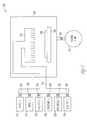
- FIG. 1shows an embodiment of an atomic layer deposition system 100 for forming a dielectric film containing dysprosium oxide doped hafnium oxide.
- a substrate 108 on a heating element/wafer holder 106is located inside a reaction chamber 102 of ALD system 100 .
- the heating element 106is thermally coupled to substrate 108 to control the substrate temperature.
- a gas-distribution fixture 110introduces precursor, reactant and purge gases to the substrate 108 in a uniform fashion.
- the gases introduced by the gas distribution fixturesometimes referred to as a showerhead, react with the substrate 108 , and any excess gas and reaction products are removed from chamber 102 by vacuum pump 104 through a control valve 105 .
- Each gasoriginates from individual gas sources 114 , 118 , 122 , 126 , 130 , and 134 , with a flow rate and time controlled by mass-flow controllers 116 , 120 , 124 , 128 , 132 and 136 , respectively.
- Gas sources 122 and 130provide a precursor gas either by storing the precursor as a gas or by providing for evaporating a solid or liquid material to form the selected precursor gas.
- purging gas sources 114 and 118are also included in the system.
- the embodimentmay use only one of the purge gases for all four disclosed illustrative purging steps, or both purge gases may be used simultaneously, or alternately as required for the particular desired result.
- additional purging gas sourcescan be constructed in ALD system 100 , one purging gas source for each different precursor and reactant gas, for example. For a process that uses the same purging gas for multiple precursor gases fewer purging gas sources may be required for ALD system 100 .
- the precursor, reactant and purge gas sourcesare coupled by their associated mass-flow controllers to a common gas line or conduit 112 , which is coupled to the gas-distribution fixture 110 inside the reaction chamber 102 .
- Gas conduit 112may also be coupled to another vacuum pump, or exhaust pump, not shown, to remove excess precursor gases, purging gases, and by-product gases at the end of a purging sequence from the gas conduit 112 .
- Vacuum pump, or exhaust pump, 104is coupled to chamber 102 by control valve 105 , which may be a mass-flow valve, to remove excess precursor gases, purging gases, and by-product gases from reaction chamber 102 at the end of a purging sequence.
- control valve 105may be a mass-flow valve, to remove excess precursor gases, purging gases, and by-product gases from reaction chamber 102 at the end of a purging sequence.
- control displays, mounting apparatus, temperature sensing devices, substrate maneuvering apparatus, and necessary electrical connections as are known to those skilled in the artare not shown in FIG. 1 .
- ALD system 100is well suited for depositing Dy doped HfO 2 films, other commercially available ALD systems may also be used.
- reaction chambersfor deposition of films are understood by those of ordinary skill in the art of semiconductor fabrication. A variety of such commercially available reaction chambers may be used. Furthermore, one of ordinary skill in the art will comprehend the necessary detection, measurement, and control techniques in the art of semiconductor fabrication upon reading and understanding the disclosure.
- ALD system 100may be controlled by a computer. To focus on the use of ALD system 100 the computer is not shown. Those skilled in the art can appreciate that the individual elements such as pressure control, temperature control, and gas flow within ALD system 100 can be under computer control.
- FIG. 2illustrates a flow diagram of operational steps for an embodiment of a method to form a nanolaminate dielectric layer containing dysprosium oxide layers alternating with hafnium oxide layers in various ways, such as nine layers of hafnium oxide and one layer of dysprosium oxide, which pattern may be repeated until a film of a desired thickness is formed.
- a substrateis prepared to react immediately with, and chemisorb the first precursor gas. This preparation will remove contaminants such as thin organic films, dirt, and native oxide from the surface of the substrate, and may include a hydrofluoric acid rinse, or a sputter etch in the reaction chamber 102 .
- a first precursor materialenters the reaction chamber for a predetermined length of time, for example 0.5-2.0 seconds.
- the first precursor materialis chemically adsorbed onto the surface of the substrate, the amount depending upon the temperature of the substrate, in one embodiment 300° C., and the presence of sufficient flow of the precursor material.
- the pulsing of the precursormay use a pulsing period that provides uniform coverage of an adsorbed monolayer on the substrate surface, or may use a pulsing period that provides partial formation of a monolayer on the substrate surface.
- a first purge gasenters the reaction chamber for a predetermined length of time sufficient to remove substantially all of the non-chemisorbed first precursor material. Typical times may be 1.0-2.0 seconds with a purge gas comprising nitrogen, argon, neon, combinations thereof, or other gases such as hydrogen.
- a first reactant gasenters the chamber for a predetermined length of time, sufficient to provide enough of the reactant to chemically combine with the amount of chemisorbed first precursor material on the surface of the substrate.
- Typical reactant materialsinclude mildly oxidizing materials, including, but not limited to, water vapor, hydrogen peroxide, nitrogen oxides, ozone and oxygen gas, and combinations thereof.
- a second purge gaswhich may be the same or different from the first purge gas, enters the chamber for a predetermined length of time, sufficient to remove substantially all non-reacted materials and any reaction byproducts from the chamber.
- a second precursor materialenters the reaction chamber for a predetermined length of time, typically 0.5-2.0 seconds.
- the second precursor materialis chemically adsorbed onto the surface of the substrate, in this case being the top surface of the first dielectric material, the amount of absorption depending upon the temperature of the substrate, and the presence of sufficient flow of the precursor material.
- the pulsing of the precursormay use a pulsing period that provides uniform coverage of an adsorbed monolayer on the substrate surface, or may use a pulsing period that provides partial formation of a monolayer on the substrate surface.
- the first purge gasis shown as entering the chamber, but the invention is not so limited.
- the purge gas used in the second dielectric material depositionmay be the same or different from either of the two previously noted purge gases, and FIG. 1 could be shown as having more than the two purge gases shown.
- the purge cyclecontinues for a predetermined length of time sufficient to remove substantially all of the non-chemisorbed second precursor material.
- a second reactant gaswhich may the same or different from the first reactant gas, enters the chamber for a predetermined length of time, sufficient to provide enough of the reactant to chemically combine with the amount of chemisorbed second precursor material on the surface of the substrate.
- another purge gasenters the chamber, which may be the same or different from any of the three previously discussed purge gases, for a predetermined length of time, sufficient to remove substantially all non-reacted materials and any reaction byproducts from the chamber.
- the desired thicknesses of the first and second dielectric materials in the dielectricmay not be the same thickness, and there may be more deposition cycles for one dielectric material as compared to the other. If the second dielectric layer has reached the desired thickness, the process moves on to a decision at 224 of whether the number of layers of the first and second dielectric materials has reached the desired number.
- a single layer of the first dielectric and a single layer of the second dielectrichave been completed at this point in the process. If more than a single layer of each dielectric material is desired, the process moves back to another deposition of the first dielectric material at 206 . After the number of interleaved layers of dielectrics one and two has reached the desired value, the deposition ends at 226 .
- the dielectric values of the RS-ALD oxides in the described embodimentare high, for example dysprosium doped hafnium oxide may have a dielectric constant of 10 to 12, and because the highly controlled layer thickness may be a single monolayer for each one of the interleaved dielectric layers, the physical thickness needed to obtain the equivalent dielectric properties of a very thin silicon dioxide layer may have from two to ten layers of the two dielectric materials described in the embodiments.
- the embodiments described hereinprovide a process for growing a dielectric film having a wide range of useful equivalent oxide thickness, t eq , associated with a dielectric constant in the range from about 10 to about 14. This range of dielectric constants provides for a t eq ranging about 33% relative to a given silicon dioxide thickness.
- an embodiment for a dysprosium doped hafnium oxidemay have a physical thickness that is three times larger than the acceptable silicon dioxide thickness, providing enhanced probability for reducing leakage current. Controlling the amount of dysprosium doping in the hafnium film in the range of 5 to 15% results in relatively low leakage current as compared to pure hafnium oxides.
- the dysprosium percentageis 10% of the haftium film.
- the novel processcan be implemented to form transistors, capacitors, memory devices, and other electronic systems including information handling devices.
- the present subject matteris not limited to two dielectric materials, and the equipment described in FIG. 1 could have included a precursor and reactant 3 , 4 , which are not described for simplicity.
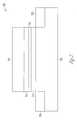
- FIG. 3illustrates a single transistor in an embodiment of a method to form a dielectric layer containing an RS-ALD deposited dysprosium doped hafnium gate oxide layer.
- a substrate 302is prepared, typically a silicon or silicon containing material. In other embodiments, germanium, gallium arsenide, silicon-on-sapphire substrates, or other suitable substrates may also be used.
- the preparation processincludes cleaning substrate 302 and forming various layers and regions of the substrate, such as drain diffusion 304 and source diffusion 306 of an illustrative metal oxide semiconductor (MOS) transistor 300 , prior to forming a gate dielectric.
- MOSmetal oxide semiconductor
- the substrateis cleaned to provide an initial substrate depleted of its native oxide.
- the initial substrateis cleaned to provide a hydrogen-terminated surface.
- a silicon substrateundergoes a final hydrofluoric (HF) rinse prior to ALD processing to provide the silicon substrate with a hydrogen-terminated surface without a native silicon oxide layer. Cleaning immediately preceding atomic layer deposition aids in reducing an occurrence of silicon oxide as an interface between silicon based substrate and dielectric formed using the atomic layer deposition process.
- the sequencing of the formation of the regions of the transistor being processedmay follow the generally understood fabrication of a MOS transistor as is well known to those skilled in the art.
- the dielectric covering the area on the substrate 302 between the source and drain diffused regions 304 and 306may be deposited by RS-ALD in this illustrative embodiment, and may comprise one or more hafnium oxide layers 310 and 314 , each potentially formed of many individual hafnium oxide layers, in an embodiment, nine layers. There is shown an interleaved dysprosium oxide layer 312 , in an embodiment, one layer. Alternatively, there may be other combinations of interleaved and non-interleaved layers of varying thickness and deposition method. This nanolaminate dielectric layer is referred to as the gate oxide, and while shown as distinct layers for clarity, is a single alloyed layer, or doped layer.
- the illustrative embodimentshows the two hafnium dielectric layers 310 and 314 having the same thickness, however the desired dielectric properties of the nanolaminate film may be best achieved by adjusting the ratio of the thickness of the two dielectric layers to different values.
- the transistor 300has a conductive material forming a gate 318 in this illustrative embodiment, but the nanolaminate dielectric may also be used in a floating gate device such as an EEPROM transistor, as either one or both of the floating gate and the control gate oxide layers.
- the conductive materialmay be polysilicon or various metals.
- the gate dielectric(layers 310 - 314 ) include a tunnel gate insulator and a floating gate dielectric in a flash memory device.
- Use of dielectric layers containing a nanolaminate atomic layer deposited dielectric layer for a gate dielectric and/or floating gate dielectric in which the dielectric layer contacts a conductive layeris not limited to silicon based substrates, but may be used with a variety of semiconductor substrates.
- a methodincludes forming a first conductive layer 402 , a second conductive layer 404 , having a nanolaminate dielectric having interleaved layers 406 - 414 of two different dielectric materials, formed between the two conductive layers.
- the conductive layers 402 and 404may include metals, doped polysilicon, silicided metals, polycides, or conductive organic compounds, without affecting the teachings of this embodiment.
- the sequencing and thickness of the individual layersdepends on the application and may include a single layer of each material, one layer of one of the materials and multiple layers of the other, or other combinations of layers including different layer thicknesses.
- a nanolaminate structurecan be engineered to have a predetermined dielectric constant and composition.
- the total thickness of layers 406 and 414is ten times the thickness of layer 410 , providing a 10% doping of layer 410 material (for example dysprosium oxide) in the layer 406 / 414 material (for example hafnium oxide).
- layer 410 materialfor example dysprosium oxide
- hafnium oxidefor example hafnium oxide
- Structures such as the nanolaminate structure shown in FIGS. 3 and 4may be used in NROM flash memory devices as well as other integrated circuits.
- Transistors, capacitors, and other devices having dielectric filmsmay be implemented into memory devices and electronic systems including information handling devices.
- Embodiments of these information handling devicesinclude wireless systems, telecommunication systems, computers and integrated circuits.
- FIG. 5illustrates a diagram for an electronic system 500 having one or more devices having a dielectric layer containing an atomic layer deposited oxide layer formed according to various embodiments.
- Electronic system 500includes a controller 502 , a bus 504 , and an electronic device 506 , where bus 504 provides electrical conductivity between controller 502 and electronic device 506 .
- controller 502 and/or electronic device 506includes an embodiment for a dielectric layer containing a nanolaminate RS-ALD deposited oxide layer as previously discussed herein.
- Electronic system 500may include, but is not limited to, information handling devices, wireless systems, telecommunication systems, fiber optic systems, electro-optic systems, and computers.
- FIG. 6depicts a diagram of an embodiment of a system 600 having a controller 602 and a memory 606 .
- Controller 602 and/or memory 606includes a dielectric layer having a nanolaminate RS-ALD dielectric layer.
- System 600also includes an electronic apparatus 608 , and a bus 604 , where bus 604 may provide electrical conductivity and data transmission between controller 602 and electronic apparatus 608 , and between controller 602 and memory 606 .
- Bus 604may include an address, a data bus, and a control bus, each independently configured.
- Bus 604also uses common conductive lines for providing address, data, and/or control, the use of which may be regulated by controller 602 .
- electronic apparatus 608includes additional memory devices configured similarly to memory 606 .
- An embodimentincludes an additional peripheral device or devices 610 coupled to bus 604 .
- controller 602is a processor. Any of controller 602 , memory 606 , bus 604 , electronic apparatus 608 , and peripheral device or devices 610 may include a dielectric layer having a nanolaminate RS-ALD deposited oxide layer in accordance with the disclosed embodiments.
- System 600may include, but is not limited to, information handling devices, telecommunication systems, and computers.
- Peripheral devices 610may include displays, additional storage memory, or other control devices that may operate in conjunction with controller 602 and/or memory 606 . It will be understood that embodiments are equally applicable to any size and type of memory circuit and are not intended to be limited to a particular type of memory device.
- Memory typesinclude a DRAM, SRAM (Static Random Access Memory) or Flash memories.
- the DRAMcould be a synchronous DRAM commonly referred to as SGRAM (Synchronous Graphics Random Access Memory), SDRAM (Synchronous Dynamic Random Access Memory), SDRAM II, and DDR SDRAM (Double Data Rate SDRAM), as well as Synchlink or Rambus DRAMs and other emerging DRAM technologies.
- SGRAMSynchronous Graphics Random Access Memory
- SDRAMSynchronous Dynamic Random Access Memory
- SDRAM IISynchroble Data Rate SDRAM
- DDR SDRAMDouble Data Rate SDRAM
- Formation of nanolaminate dysprosium doped hafnium oxide layers by a nanolaminate RS-ALD depositionmay be realized using a diketonate type chelate precursor chemical, such as Dy(thd) 3 , and an oxidizing precursor, such as ozone. Further, such doped dielectric films formed by RS-ALD processed in relatively low temperatures, such as 300° C. or even 160° C., may be amorphous and possess smooth surfaces. Such RS-ALD oxide films may provide enhanced electrical properties as compared to physical deposition methods, such as sputtering or typical chemical layer depositions, due to their smoother surface, and reduced damage, resulting in reduced leakage current.
- dielectric layersprovide a significantly thicker physical thickness than a silicon oxide layer having the same equivalent oxide thickness, where the increased thickness may also reduce leakage current issues.
- Dysprosium doped hafnium oxideshave beneficial properties for gate dielectrics and capacitor dielectric materials including thermal stability, high dielectric constant and low leakage currents.
- the conductive layers contacting the dielectricmay include metals, semiconductor materials, polycrystalline semiconductor materials and doped materials of either conductivity type.
- Capacitors, transistors, higher level ICs or devices including memory devices, and electronic systemsare constructed utilizing the novel process for forming a dielectric film having an ultra thin equivalent oxide thickness, t eq .
- Gate dielectric layers or films containing atomic layer deposited lanthanide oxideare formed having a dielectric constant ( ⁇ ) substantially higher than that of silicon oxide, such that these dielectric films possess an equivalent thickness, t eq , thinner than SiO 2 gate dielectrics of the same physical thickness.
- the high dielectric constant relative to silicon dioxideallows the use of much larger physical thickness of these high- ⁇ dielectric materials for the same t eq of SiO 2 .
- Film having the relatively larger physical thicknessaids in processing gate dielectrics and other dielectric layers in electronic devices and systems, and improves the electrical properties of the dielectrics.
Landscapes
- Chemical & Material Sciences (AREA)
- Engineering & Computer Science (AREA)
- General Chemical & Material Sciences (AREA)
- Chemical Kinetics & Catalysis (AREA)
- Condensed Matter Physics & Semiconductors (AREA)
- General Physics & Mathematics (AREA)
- Manufacturing & Machinery (AREA)
- Computer Hardware Design (AREA)
- Microelectronics & Electronic Packaging (AREA)
- Power Engineering (AREA)
- Physics & Mathematics (AREA)
- Organic Chemistry (AREA)
- Materials Engineering (AREA)
- Mechanical Engineering (AREA)
- Metallurgy (AREA)
- Crystallography & Structural Chemistry (AREA)
- Inorganic Chemistry (AREA)
- Formation Of Insulating Films (AREA)
- Semiconductor Memories (AREA)
- Insulated Gate Type Field-Effect Transistor (AREA)
Abstract
Description
- This application relates generally to semiconductor devices and device fabrication and, more particularly, to dielectric layers and their method of fabrication.
- The semiconductor device industry has a market driven need to reduce the size of devices such as transistors. To reduce transistor size, the thickness of the silicon dioxide, SiO2, gate dielectric is reduced in proportion to the shrinkage of the gate length. For example, a metal-oxide-semiconductor field effect transistor (MOSFET) would use a 1.5 nm thick SiO2gate dielectric for a gate length of less than 100 nm. Such scaling of gate dielectrics may be the most difficult issue facing the production of the next generation of MOSFETs. The increasingly small and reliable integrated circuits (ICs) will likely be used in products such as processor chips, mobile telephones, and memory devices such as dynamic random access memories (DRAMs).
- Currently, the semiconductor industry relies on the ability to reduce or scale all of the dimensions of its basic devices, such as the silicon based MOSFET, to achieve the required improved operation. This device scaling includes scaling the gate dielectric, which has primarily been formed of silicon dioxide (SiO2). A thermally grown amorphous SiO2layer provides an electrically and thermodynamically stable material, where the interface of the SiO2layer with underlying silicon provides a high quality interface as well as superior electrical isolation properties. However, increased scaling and other requirements in microelectronic devices have created problems as the gate dielectric has become thinner, and generated the need to use other dielectric materials as gate dielectrics, in particular dielectric materials with higher dielectric constants (k).
- The above mentioned problems are addressed by the present invention and will be understood by reading and studying the following specification. An embodiment for a method for forming an electronic device includes forming a dielectric layer by using an atomic layer deposition (ALD) technique to form a dielectric having dysprosium oxide (for example Dy2O3) doped hafnium oxide (for example HfO2). An embodiment includes forming an integrated circuit having a dielectric layer made by using an atomic layer deposition to form dysprosium oxide doped hafnium oxide, and having a conductive layer on the dielectric layer. Another embodiment includes a method of forming a memory array having an atomic layer deposited dielectric layer of dysprosium oxide doped hafnium oxide, contacting a conductive layer and forming an address decoder coupled to the memory array.
- Embodiments include structures for capacitors, transistors, memory devices, and electronic systems with dielectric layers containing an atomic layer deposited dysprosium doped hafnium oxide dielectric, and methods for forming such structures. These and other aspects, embodiments, advantages, and features will become apparent from the following description and the referenced drawings.
FIG. 1 depicts an atomic layer deposition system for fabricating a dielectric layer formed as a nanolaminate layered sequence of dysprosium oxide and hafnium oxide, according to various embodiments;FIG. 2 illustrates a flow diagram of elements for an embodiment of a method to form a dielectric layer containing dysprosium doped hafnium oxide by atomic layer deposition according to various embodiments;FIG. 3 illustrates an embodiment of a configuration of a transistor having a dielectric layer containing an atomic layer deposited dielectric layer containing dysprosium doped hafnium oxide;FIG. 4 shows an embodiment of a configuration of a capacitor having a dielectric layer containing an atomic layer deposited dysprosium doped hafnium oxide;FIG. 5 is a simplified diagram for an embodiment of a controller coupled to an electronic device; andFIG. 6 illustrates a diagram for an embodiment of an electronic system having devices with a dielectric film containing an atomic layer deposited nanolaminate layered sequence of praseodymium oxide and zirconium oxide dielectric layer.- The following detailed description refers to the accompanying drawings that show, by way of illustration, specific aspects and embodiments in which the present invention may be practiced. These embodiments are described in sufficient detail to enable those skilled in the art to practice the present invention. Other embodiments may be utilized and structural, logical, and electrical changes may be made without departing from the scope of the present invention. The various embodiments are not necessarily mutually exclusive, as some embodiments can be combined with one or more other embodiments to form new embodiments.
- The terms wafer and substrate used in the following description include any structure having an exposed surface with which to form an integrated circuit (IC) structure. The term substrate is understood to include semiconductor wafers. The term substrate is also used to refer to semiconductor structures during processing, and may include other layers that have been fabricated thereupon. Both wafer and substrate include doped and undoped semiconductors, epitaxial semiconductor layers supported by a base semiconductor or insulator, as well as other semiconductor structures well known to one skilled in the art. The term conductor is understood to generally include n-type and p-type semiconductors and the term insulator or dielectric is defined to include any material that is less electrically conductive than the materials referred to as conductors or as semiconductors.
- The term “horizontal” as used in this application is defined as a plane parallel to the conventional plane or surface of a wafer or substrate, regardless of the orientation of the wafer or substrate. The term “vertical” refers to a direction perpendicular to the horizontal as defined above. Prepositions, such as “on”, “side” (as in “sidewall”), “higher”, “lower”, “over” and “under” are defined with respect to the conventional plane or surface being on the top surface of the wafer or substrate, regardless of the orientation of the wafer or substrate. The following detailed description is, therefore, not to be taken in a limiting sense, and the scope of the present invention is defined only by the appended claims, along with the full scope of equivalents to which such claims are entitled.
- Dysprosium is elemental metal number66 and is part of the lanthanide series of elements. Hafnium is elemental metal number72, and is situated next to tantalum and right after the lanthanide metals on the periodic table of elements. Hafnium oxide films can be atomic layer deposited using various precursors such as hafnium tetraiodide and oxygen at a temperature of between 400 to 700 degrees C., or hafnium tetrachloride and steam at 300 degrees C., or anhydrous hafnium nitride (Hf(NO3)4) and ozone at 160 degrees C. Dysprosium oxide films can be atomic layer deposited using various precursors such as volatile diketonate chelates (for example 2,2,6,6-tetramethyl-3,5-heptanedione) and ozone at 300 degrees C. Each of these films may have a very tightly controlled thickness for each deposition cycle that depends on the saturation of the substrate surface. For example the hafnium oxide layers may be typically 0.14 nm thick per deposition cycle. If repetitive layers of hafnium oxide are grown upon one another, then the single resulting film of hafnium oxide will have a thickness that is easily controlled by simply controlling the number of deposition cycles run. The surface of the ALD formed is also very smooth and continuous, even over sharp underlying topography. The deposition cycles may also be alternated between the two different oxides and the resulting film may either be a nanolaminate of the two, or more, different oxides, or the oxides may form an alloy with each other if the similarity between the two metals results in miscible materials. In either case the film properties may vary depending upon the ratio of the two or more different materials, and thus materials may be formed that have engineered properties. For example, to form a 10% dysprosium alloy with hafnium oxide, deposit nine layers of hafnium oxide and then one layer of dysprosium oxide and repeat until the desired thickness is achieved.
- The dielectric structure is formed by depositing hafnium by atomic layer deposition onto a substrate surface using precursor chemicals to form a film of HfO2, followed by ALD depositing dysprosium onto the substrate using precursor chemicals to form Dy2O3, and repeating as often as necessary to form a dielectric structure of the required thickness. An alloyed dielectric layer of dysprosium oxide and hafnium oxide may be beneficially used because the relatively high dielectric constant (high-k) of 10-12 of the film, as compared to 3.9 for silicon dioxide, and the excellent current leakage value, provides the functionality of a much thinner silicon dioxide film without the reliability loss consequent to using such physically thin films.
- A gate dielectric in a transistor has both a physical gate dielectric thickness and an equivalent oxide thickness (teq). The equivalent oxide thickness quantifies the electrical properties, such as capacitance, of the gate dielectric in terms of a representative physical thickness. teqis defined as the thickness of a theoretical SiO2layer that would be required to have the same capacitance density as a given dielectric, ignoring leakage current and reliability considerations.
- A SiO2layer of thickness, t, deposited on a Si surface as a gate dielectric will have a teqlarger than its thickness, t. This teqresults from the capacitance in the surface channel on which the SiO2is deposited due to the formation of a depletion/inversion region. This depletion/inversion region can result in teqbeing from 3 to 6 Angstroms (↑) larger than the SiO2thickness, t. Thus, with the semiconductor industry driving to someday scale the gate dielectric equivalent oxide thickness to under 10 Å, the physical thickness requirement for a SiO2layer used for a gate dielectric would be need to be approximately 4 to 7 Å.
- Additional requirements on a SiO2layer would depend on the gate electrode used in conjunction with the SiO2gate dielectric. Using a conventional polysilicon gate would result in an additional increase in teqfor the SiO2layer. This additional thickness could be eliminated by using a metal gate electrode, though metal gates are not currently used in typical complementary metal-oxide-semiconductor field effect transistor (CMOS) technology. Thus, future devices would be designed towards a physical SiO2gate dielectric layer of about 5 Å or less.
- Silicon dioxide is used as a gate dielectric, in part, due to its electrical isolation properties in a SiO2—Si based structure. This electrical isolation is due to the relatively large band gap of SiO2(8.9 eV), which makes it a good insulator. Significant reductions in its band gap would eliminate it as a material for use as a gate dielectric. However, as the thickness of a SiO2layer decreases, the number of atomic layers, or monolayers of the material in the thickness decreases. At a certain thickness, the number of monolayers will be sufficiently small that the SiO2layer will not have a complete arrangement of atoms as in a thicker or bulk layer. As a result of incomplete formation relative to a bulk structure, a thin SiO2layer of only one or two monolayers will not form a full band gap. The lack of a full band gap in a SiO2gate dielectric may cause an effective short between an underlying conductive silicon channel and an overlying polysilicon gate. This undesirable property sets a limit on the physical thickness to which a SiO2layer can be scaled. The minimum thickness due to this monolayer effect is thought to be about 7-8 Å. Therefore, for future devices to have a teqless than about 10 Å, other dielectrics than SiO2need to be considered for use as a gate dielectric.
- For a typical dielectric layer used as a gate dielectric, the capacitance is determined as one for a parallel plate capacitance: C=κε0A/t, where κ is the dielectric constant, ε0is the permittivity of free space, A is the area of the capacitor, and t is the thickness of the dielectric. The thickness, t, of a material is related to its teqfor a given capacitance, with SiO2having a dielectric constant κox=3.9, as
t=(κ/κox)teq=(κ/3.9)teq.
Thus, materials with a dielectric constant greater than that of SiO2will have a physical thickness that can be considerably larger than a desired teq, while providing the desired equivalent oxide thickness. For example, an alternate dielectric material with a dielectric constant of 10 could have a thickness of about 25.6 Å to provide a teqof 10 Å, not including any depletion/inversion layer effects. Thus, a reduced equivalent oxide thickness for transistors can be realized by using dielectric materials with higher dielectric constants than SiO2. - The thinner equivalent oxide thickness required for lower transistor operating voltages and smaller transistor dimensions may be realized by a significant number of materials, but additional fabricating requirements makes determining a suitable replacement for SiO2difficult. The current view for the future of the microelectronics industry still predicts silicon based devices. This requires that the gate dielectric employed be grown on a silicon substrate or silicon layer, which places significant constraints on the substitute dielectric material. During the formation of the dielectric on the silicon layer, there exists the possibility that a small layer of SiO2could be formed in addition to the desired dielectric. The result would effectively be a dielectric layer consisting of two sub-layers in parallel with each other and the silicon layer on which the dielectric is formed. In such a case, the resulting capacitance would be that of two dielectrics in series. As a result, the teqof the dielectric layer would be the sum of the SiO2thickness and a multiplicative factor of the thickness, t, of the dielectric being formed, written as
teq=tSiO2 +(κox/κ)t.
Thus, if a SiO2layer is formed in the process, the teqis again limited by a SiO2layer. In the event that a barrier layer is formed between the silicon layer and the desired dielectric in which the barrier layer prevents the formation of a SiO2layer, the teqwould be limited by the layer with the lowest dielectric constant. However, whether a single dielectric layer with a high dielectric constant or a barrier layer with a higher dielectric constant than SiO2is employed, the layer directly in contact, or interfacing with the silicon layer must provide a high quality interface to maintain high channel carrier mobility. - One of the advantages of using SiO2as a gate dielectric has been that the formation of the SiO2layer results in an amorphous gate dielectric. Having an amorphous structure for a gate dielectric provides reduced leakage current problems associated with grain boundaries in polycrystalline gate dielectrics, which may cause high leakage paths. Additionally, grain size and orientation changes throughout a polycrystalline gate dielectric can cause variations in the film's dielectric constant, along with uniformity and surface topography problems. Typically, materials having the advantage of a high dielectric constant relative to SiO2also have the disadvantage of a crystalline form, at least in a bulk configuration. The best candidates for replacing SiO2as a gate dielectric are those with high dielectric constant, which can be fabricated as a thin layer with an amorphous form.
- Candidates to replace SiO2include high-κ dielectric materials. High-κ materials include materials having a dielectric constant greater than silicon dioxide, for example, dielectric materials having a dielectric constant greater than about twice the dielectric constant of silicon dioxide. An appropriate high-κ gate dielectric should have a large energy gap (Eg) and large energy barrier heights with the silicon substrate for both electrons and holes. Generally, the band gap is inversely related to the dielectric constant for a high-K material, which lessens some advantages of the high-κ material. A set of high-κ dielectric candidates for replacing silicon oxide as the dielectric material in electronic components in integrated circuit includes the lanthanide oxides such as Pr2O3, La2O3, Nd2O3, Sm2O3, Gd2O3, Dy2O3, Ce2O3, Tb2O3, Er2O3, Eu2O3, Lu2O3, Tm2O3, Ho2O3, Pm2O3, and Yb2O3. Other candidates include various lanthanide silicates, zirconium oxide ZrO2, and hafnium oxide HfO2, which as previously noted is element number72, and the first element after the end of the lanthanide series of the periodic table of elements. Such high dielectric constant layers provide a significantly thinner equivalent oxide thickness compared with a silicon oxide layer having the same physical thickness. Alternately, such dielectric layers provide a significantly thicker physical thickness than a silicon oxide layer having the same equivalent oxide thickness. This increased physical thickness aids in reducing leakage current.
- Another consideration for selecting the material and method for forming a dielectric film for use in electronic devices and systems concerns the roughness of a dielectric film on a substrate. Surface roughness of the dielectric film has a significant effect on the electrical properties of the gate oxide, and the resulting operating characteristics of the transistor. The leakage current through a physical 1.0 nm gate dielectric may increase by a factor of 10 for every 0.1 increase in the root-mean-square (RMS) roughness of the dielectric layer.
- During a conventional sputtering deposition process, particles of the material to be deposited bombard the surface at a high energy. When a particle hits the surface, some particles adhere, and other particles cause damage. High energy impacts remove body region particles, creating pits. The surface of such a deposited layer may have a rough contour due to the rough interface at the body region.
- In an embodiment, a dielectric film having a substantially smooth surface relative to other processing techniques is formed using atomic layer deposition (ALD). Further, forming such a dielectric film using atomic layer deposition can provide for controlling transitions between material layers. As a result of such control, atomic layer deposited dielectric film may have an engineered transition with a substrate surface, or may be formed with many thin layers of different dielectric materials to enable selection of the dielectric constant to a value between that available from pure dielectric compounds.
- ALD, which may be known as atomic layer epitaxy (ALE), is a modification of chemical vapor deposition (CVD) and may also be called “alternatively pulsed-CVD.” In ALD, gaseous precursors are introduced one at a time to the substrate surface mounted within a reaction chamber (or reactor). This introduction of the gaseous precursors takes the form of pulses of each gaseous precursor. In a pulse of a precursor gas, the precursor gas is made to flow into a specific area or region for a short period of time. Between the pulses, the reaction chamber is purged with a gas, which in many cases is an inert gas, and/or evacuated.
- In the first reaction step of the ALD process the first precursor saturates and is chemisorbed at the substrate surface, during the first pulsing phase. Subsequent pulsing with a purging gas removes excess precursor from the reaction chamber, specifically the precursor that has not been chemisorbed.
- The second pulsing phase introduces a second precursor to the substrate where the growth reaction of the desired film takes place, with a reaction thickness that depends upon the amount of the chemisorbed first precursor. Subsequent to the film growth reaction, reaction byproducts and precursor excess are purged from the reaction chamber. With a precursor chemistry where the precursors adsorb and react with each other on the substrate aggressively, one ALD cycle can be performed in less than one second in properly designed flow type reaction chambers. Typically, precursor pulse times range from about 0.5 sec to about 2 to 3 seconds.
- In ALD processes, the saturation of all the reaction and purging phases makes the film growth self-limiting. This self-limiting growth results in large area uniformity and conformality, which has important applications for such cases as planar substrates, deep trenches, and in the processing of porous silicon and high surface area silica and alumina powders. Significantly, ALD provides for controlling film thickness in a straightforward manner by controlling the number of growth cycles.
- ALD was originally developed to manufacture luminescent and dielectric films needed in electroluminescent displays. Significant efforts have been made to apply ALD to the growth of doped zinc sulfide and alkaline earth metal sulfide films. Additionally, ALD has been studied for the growth of different epitaxial II-V and II-VI films, nonepitaxial crystalline or amorphous oxide and nitride films and multilayer structures of these. There also has been considerable interest towards the ALD growth of silicon and germanium films, but due to the difficult precursor chemistry, this has not been very successful.
- The precursors used in an ALD process may be gaseous, liquid or solid. However, liquid or solid precursors should be volatile with high vapor pressures or low sublimation temperatures. The vapor pressure should be high enough for effective mass transportation. In addition, solid and some liquid precursors may need to be heated inside the reaction chamber and introduced through heated tubes to the substrates. The necessary vapor pressure should be reached at a temperature below the substrate temperature to avoid the condensation of the precursors on the substrate. Due to the self-limiting growth mechanisms of ALD, relatively low vapor pressure solid precursors may be used, though evaporation rates may vary somewhat during the process because of changes in their surface area.
- There are several other characteristics for precursors used in ALD. The precursors should be thermally stable at the substrate temperature because their decomposition would destroy the surface control and accordingly the advantages of the ALD method that relies on the reaction of the precursor at the substrate surface. A slight decomposition, if slow compared to the ALD growth, can be tolerated.
- The precursors should chemisorb on, or react with the surface, though the interaction between the precursor and the surface as well as the mechanism for the adsorption is different for different precursors. The molecules at the substrate surface should react aggressively with the second precursor, which may be called a reactant, to form the desired solid film. Additionally, precursors should not react with the film to cause etching, and precursors should not dissolve in the film. The use of highly reactive precursors in ALD may contrast with the precursors for conventional metallo-organic CVD (MOCVD) type reactions.
- The by-products in the reaction should be gaseous in order to allow their easy removal from the reaction chamber during a purge stage. Further, the by-products should not react or adsorb on the surface.
- In a reaction sequence ALD (RS-ALD) process, the self-limiting process sequence involves sequential surface chemical reactions. RS-ALD relies on chemistry between a reactive surface and a reactive molecular precursor. In an RS-ALD process, molecular precursors are pulsed into the ALD reaction chamber separately. The metal precursor reaction at the substrate is typically followed by an inert gas pulse (or purge) to remove excess precursor and by-products from the reaction chamber prior to an input pulse of the next precursor of the fabrication sequence.
- By the use of RS-ALD processes, films can be layered in equal metered sequences that are all identical in chemical kinetics, deposition per cycle, composition, and thickness. RS-ALD sequences generally deposit less than a full layer of the deposited material (for example hafnium oxide) per deposition cycle. Typically, a deposition or growth rate of about 0.25 to about 2.00 Å per RS-ALD cycle can be realized.
- The advantages of RS-ALD include continuity at an interface avoiding poorly defined nucleating regions that are typical for thin chemical vapor deposition (<20 Å) and physical vapor deposition (<50 Å), conformality over a variety of substrate topologies due to its layer-by-layer deposition technique, use of low temperature and mildly oxidizing processes, lack of dependence on the reaction chamber, growth thickness dependent solely on the number of cycles performed, and ability to engineer multilayer laminate films with resolution of one to two monolayers. RS-ALD processes allow for deposition control on the order of single monolayers and the ability to deposit monolayers of amorphous films.
- A cycle of an ALD deposition sequence includes pulsing a precursor material, pulsing a purging gas for the precursor, pulsing a reactant precursor, and pulsing the reactant's purging gas, resulting in a very consistent deposition thickness that depends upon the amount of the first precursor that adsorbs onto, and saturates, the surface. This cycle may be repeated until the desired thickness is achieved in a single material dielectric layer, or may be alternated with pulsing a third precursor material, pulsing a purging gas for the third precursor, pulsing a fourth reactant precursor, and pulsing the fourth reactant's purging gas. In the case where the thickness of the first series of cycles results in a dielectric layer that is only a few molecular layers thick, and the second series of cycles also results in a different dielectric layer that is only a few molecular layers thick, this may be known as a nanolayer material or a nanolaminate. A nanolaminate means a composite film of ultra thin layers of two or more different materials in a layered stack, where the layers are alternating layers of the different materials having a thickness on the order of a nanometer, and may be a continuous film only a single monolayer thick of the material. The nanolayers are not limited to alternating single layers of each material, but may include having several layers of one material alternating with a single layer of the other material, to obtain a desired ratio of the two or more materials. Such an arrangement may obtain a dielectric constant that is between the values of the two or more materials singly. A nanolaminate may also include having several layers of one material formed by an ALD reaction either over or under a single layer of a different material formed by another type of reaction, such as a MOCVD reaction. The layers of different materials may remain separate after deposition, or they may react with each other to form an alloy layer.
- In an embodiment, a nanolaminate layer of hafnium oxide is formed on a substrate mounted in a reaction chamber using RS-ALD. Alternatively, multiple layers may be formed in a repetitive sequence using precursor gases individually pulsed into the reaction chamber. An embodiment includes forming the hafnium oxide layers using a precursor gas such as hafnium tetra-iodide having a chemical formula of HfI4, or hafnium tetra-chloride having a formula of HfCl4, or anhydrous hafnium nitride having a formula of Hf(NO3)4. An embodiment includes forming the dysprosium oxide using a diketonate chelate precursor gas such as tetramethyl heptanedione or dipivaloylmethane. Other solid or liquid precursors may be used in an appropriately designed reaction chamber. The use of such precursors in an RS-ALD reaction chamber may result in lower deposition temperatures in the range of 160 to 300 degrees Celsius, and the ability to use mildly oxidizing reactant materials such as H2O, H2O2, various alcohols, N2O, ozone or oxygen. Purge gases may include nitrogen, helium, argon or neon. The dysprosium doped hafnium films formed may have good thermal and electrical properties, with a high dielectric constant k=10 to 12. Such films may survive high temperature anneals (sometimes used to reduce fixed surface state charges and improve metal to semiconductor resistance) of up to 1000 degrees Celsius, and have low leakage currents of less than 2×10⁻⁷A/cm2at electric field strengths of one MVolts/cm.
FIG. 1 shows an embodiment of an atomiclayer deposition system 100 for forming a dielectric film containing dysprosium oxide doped hafnium oxide. InFIG. 1 , asubstrate 108 on a heating element/wafer holder 106 is located inside areaction chamber 102 ofALD system 100. Theheating element 106 is thermally coupled tosubstrate 108 to control the substrate temperature. A gas-distribution fixture 110 introduces precursor, reactant and purge gases to thesubstrate 108 in a uniform fashion. The gases introduced by the gas distribution fixture, sometimes referred to as a showerhead, react with thesubstrate 108, and any excess gas and reaction products are removed fromchamber 102 byvacuum pump 104 through acontrol valve 105. Each gas originates fromindividual gas sources flow controllers Gas sources - Also included in the system are purging
gas sources flow controllers ALD system 100, one purging gas source for each different precursor and reactant gas, for example. For a process that uses the same purging gas for multiple precursor gases fewer purging gas sources may be required forALD system 100. The precursor, reactant and purge gas sources are coupled by their associated mass-flow controllers to a common gas line orconduit 112, which is coupled to the gas-distribution fixture 110 inside thereaction chamber 102.Gas conduit 112 may also be coupled to another vacuum pump, or exhaust pump, not shown, to remove excess precursor gases, purging gases, and by-product gases at the end of a purging sequence from thegas conduit 112. - Vacuum pump, or exhaust pump,104 is coupled to
chamber 102 bycontrol valve 105, which may be a mass-flow valve, to remove excess precursor gases, purging gases, and by-product gases fromreaction chamber 102 at the end of a purging sequence. For convenience, control displays, mounting apparatus, temperature sensing devices, substrate maneuvering apparatus, and necessary electrical connections as are known to those skilled in the art are not shown inFIG. 1 . ThoughALD system 100 is well suited for depositing Dy doped HfO2films, other commercially available ALD systems may also be used. - The use, construction and operation of reaction chambers for deposition of films are understood by those of ordinary skill in the art of semiconductor fabrication. A variety of such commercially available reaction chambers may be used. Furthermore, one of ordinary skill in the art will comprehend the necessary detection, measurement, and control techniques in the art of semiconductor fabrication upon reading and understanding the disclosure.
- The elements of
ALD system 100 may be controlled by a computer. To focus on the use ofALD system 100 the computer is not shown. Those skilled in the art can appreciate that the individual elements such as pressure control, temperature control, and gas flow withinALD system 100 can be under computer control. FIG. 2 illustrates a flow diagram of operational steps for an embodiment of a method to form a nanolaminate dielectric layer containing dysprosium oxide layers alternating with hafnium oxide layers in various ways, such as nine layers of hafnium oxide and one layer of dysprosium oxide, which pattern may be repeated until a film of a desired thickness is formed. At202, a substrate is prepared to react immediately with, and chemisorb the first precursor gas. This preparation will remove contaminants such as thin organic films, dirt, and native oxide from the surface of the substrate, and may include a hydrofluoric acid rinse, or a sputter etch in thereaction chamber 102. At206 a first precursor material enters the reaction chamber for a predetermined length of time, for example 0.5-2.0 seconds. The first precursor material is chemically adsorbed onto the surface of the substrate, the amount depending upon the temperature of the substrate, in oneembodiment 300° C., and the presence of sufficient flow of the precursor material. In addition, the pulsing of the precursor may use a pulsing period that provides uniform coverage of an adsorbed monolayer on the substrate surface, or may use a pulsing period that provides partial formation of a monolayer on the substrate surface.- At208 a first purge gas enters the reaction chamber for a predetermined length of time sufficient to remove substantially all of the non-chemisorbed first precursor material. Typical times may be 1.0-2.0 seconds with a purge gas comprising nitrogen, argon, neon, combinations thereof, or other gases such as hydrogen. At210 a first reactant gas enters the chamber for a predetermined length of time, sufficient to provide enough of the reactant to chemically combine with the amount of chemisorbed first precursor material on the surface of the substrate. Typical reactant materials include mildly oxidizing materials, including, but not limited to, water vapor, hydrogen peroxide, nitrogen oxides, ozone and oxygen gas, and combinations thereof. At212 a second purge gas, which may be the same or different from the first purge gas, enters the chamber for a predetermined length of time, sufficient to remove substantially all non-reacted materials and any reaction byproducts from the chamber.
- At214 a decision is made as to whether or not the thickness of the first dielectric material in the dielectric has reached the desired thickness, or whether another deposition cycle is required. If another deposition cycle is needed, then the operation returns to206, until the desired first dielectric layer is completed, at which time the process moves on to the deposition of the second material at215. At215 a second precursor material enters the reaction chamber for a predetermined length of time, typically 0.5-2.0 seconds. The second precursor material is chemically adsorbed onto the surface of the substrate, in this case being the top surface of the first dielectric material, the amount of absorption depending upon the temperature of the substrate, and the presence of sufficient flow of the precursor material. In addition, the pulsing of the precursor may use a pulsing period that provides uniform coverage of an adsorbed monolayer on the substrate surface, or may use a pulsing period that provides partial formation of a monolayer on the substrate surface.
- At216 the first purge gas is shown as entering the chamber, but the invention is not so limited. The purge gas used in the second dielectric material deposition may be the same or different from either of the two previously noted purge gases, and
FIG. 1 could be shown as having more than the two purge gases shown. The purge cycle continues for a predetermined length of time sufficient to remove substantially all of the non-chemisorbed second precursor material. - At218 a second reactant gas, which may the same or different from the first reactant gas, enters the chamber for a predetermined length of time, sufficient to provide enough of the reactant to chemically combine with the amount of chemisorbed second precursor material on the surface of the substrate. At220 another purge gas enters the chamber, which may be the same or different from any of the three previously discussed purge gases, for a predetermined length of time, sufficient to remove substantially all non-reacted materials and any reaction byproducts from the chamber.
- At222 a decision is made as to whether or not the thickness of the second dielectric material in the nanolaminate dielectric has reached the desired thickness, or whether another deposition cycle is required. If another deposition cycle is needed, then the operation returns to215, until the desired second dielectric layer is completed. The desired thicknesses of the first and second dielectric materials in the dielectric may not be the same thickness, and there may be more deposition cycles for one dielectric material as compared to the other. If the second dielectric layer has reached the desired thickness, the process moves on to a decision at224 of whether the number of layers of the first and second dielectric materials has reached the desired number. In this illustrative embodiment, a single layer of the first dielectric and a single layer of the second dielectric have been completed at this point in the process. If more than a single layer of each dielectric material is desired, the process moves back to another deposition of the first dielectric material at206. After the number of interleaved layers of dielectrics one and two has reached the desired value, the deposition ends at226. Because the dielectric values of the RS-ALD oxides in the described embodiment are high, for example dysprosium doped hafnium oxide may have a dielectric constant of 10 to 12, and because the highly controlled layer thickness may be a single monolayer for each one of the interleaved dielectric layers, the physical thickness needed to obtain the equivalent dielectric properties of a very thin silicon dioxide layer may have from two to ten layers of the two dielectric materials described in the embodiments.
- The embodiments described herein provide a process for growing a dielectric film having a wide range of useful equivalent oxide thickness, teq, associated with a dielectric constant in the range from about 10 to about 14. This range of dielectric constants provides for a teqranging about 33% relative to a given silicon dioxide thickness. For an acceptable equivalent silicon dioxide thickness, an embodiment for a dysprosium doped hafnium oxide may have a physical thickness that is three times larger than the acceptable silicon dioxide thickness, providing enhanced probability for reducing leakage current. Controlling the amount of dysprosium doping in the hafnium film in the range of 5 to 15% results in relatively low leakage current as compared to pure hafnium oxides. In an embodiment, the dysprosium percentage is 10% of the haftium film. Additionally, the novel process can be implemented to form transistors, capacitors, memory devices, and other electronic systems including information handling devices. The present subject matter is not limited to two dielectric materials, and the equipment described in
FIG. 1 could have included a precursor and reactant3,4, which are not described for simplicity. FIG. 3 illustrates a single transistor in an embodiment of a method to form a dielectric layer containing an RS-ALD deposited dysprosium doped hafnium gate oxide layer. This embodiment may be implemented with thesystem 100 ofFIG. 1 used as an atomic layer deposition system. Asubstrate 302 is prepared, typically a silicon or silicon containing material. In other embodiments, germanium, gallium arsenide, silicon-on-sapphire substrates, or other suitable substrates may also be used. The preparation process includes cleaningsubstrate 302 and forming various layers and regions of the substrate, such asdrain diffusion 304 andsource diffusion 306 of an illustrative metal oxide semiconductor (MOS)transistor 300, prior to forming a gate dielectric. In an embodiment, the substrate is cleaned to provide an initial substrate depleted of its native oxide. In an embodiment, the initial substrate is cleaned to provide a hydrogen-terminated surface. In an embodiment, a silicon substrate undergoes a final hydrofluoric (HF) rinse prior to ALD processing to provide the silicon substrate with a hydrogen-terminated surface without a native silicon oxide layer. Cleaning immediately preceding atomic layer deposition aids in reducing an occurrence of silicon oxide as an interface between silicon based substrate and dielectric formed using the atomic layer deposition process. The sequencing of the formation of the regions of the transistor being processed may follow the generally understood fabrication of a MOS transistor as is well known to those skilled in the art.- The dielectric covering the area on the
substrate 302 between the source and drain diffusedregions dysprosium oxide layer 312, in an embodiment, one layer. Alternatively, there may be other combinations of interleaved and non-interleaved layers of varying thickness and deposition method. This nanolaminate dielectric layer is referred to as the gate oxide, and while shown as distinct layers for clarity, is a single alloyed layer, or doped layer. There may be a diffusion barrier layer inserted between thefirst dielectric layer 310 and thesubstrate 302 to prevent metal contamination from affecting the electrical properties of the device. The illustrative embodiment shows the two hafnium dielectric layers310 and314 having the same thickness, however the desired dielectric properties of the nanolaminate film may be best achieved by adjusting the ratio of the thickness of the two dielectric layers to different values. Thetransistor 300 has a conductive material forming agate 318 in this illustrative embodiment, but the nanolaminate dielectric may also be used in a floating gate device such as an EEPROM transistor, as either one or both of the floating gate and the control gate oxide layers. The conductive material may be polysilicon or various metals. - In an illustrative embodiment, the gate dielectric (layers310-314) include a tunnel gate insulator and a floating gate dielectric in a flash memory device. Use of dielectric layers containing a nanolaminate atomic layer deposited dielectric layer for a gate dielectric and/or floating gate dielectric in which the dielectric layer contacts a conductive layer is not limited to silicon based substrates, but may be used with a variety of semiconductor substrates.
- The embodiments of methods for forming dielectric layers containing a RS-ALD deposited dielectric layer contacting a conductive layer may also be applied to forming capacitors in various integrated circuits, memory devices, and electronic systems. In an embodiment including a
capacitor 400 illustrated inFIG. 4 , a method includes forming a firstconductive layer 402, a secondconductive layer 404, having a nanolaminate dielectric having interleaved layers406-414 of two different dielectric materials, formed between the two conductive layers. Theconductive layers layers 406 and414 is ten times the thickness oflayer 410, providing a 10% doping oflayer 410 material (for example dysprosium oxide) in the layer406/414 material (for example hafnium oxide). Although the oxide layers are shown in this illustrative example as being distinct layers, the oxide may be alloyed together to form a single material layer. Structures such as the nanolaminate structure shown inFIGS. 3 and 4 may be used in NROM flash memory devices as well as other integrated circuits. Transistors, capacitors, and other devices having dielectric films may be implemented into memory devices and electronic systems including information handling devices. Embodiments of these information handling devices include wireless systems, telecommunication systems, computers and integrated circuits. FIG. 5 illustrates a diagram for anelectronic system 500 having one or more devices having a dielectric layer containing an atomic layer deposited oxide layer formed according to various embodiments.Electronic system 500 includes acontroller 502, abus 504, and anelectronic device 506, wherebus 504 provides electrical conductivity betweencontroller 502 andelectronic device 506. In various embodiments,controller 502 and/orelectronic device 506 includes an embodiment for a dielectric layer containing a nanolaminate RS-ALD deposited oxide layer as previously discussed herein.Electronic system 500 may include, but is not limited to, information handling devices, wireless systems, telecommunication systems, fiber optic systems, electro-optic systems, and computers.FIG. 6 depicts a diagram of an embodiment of asystem 600 having acontroller 602 and amemory 606.Controller 602 and/ormemory 606 includes a dielectric layer having a nanolaminate RS-ALD dielectric layer.System 600 also includes anelectronic apparatus 608, and abus 604, wherebus 604 may provide electrical conductivity and data transmission betweencontroller 602 andelectronic apparatus 608, and betweencontroller 602 andmemory 606.Bus 604 may include an address, a data bus, and a control bus, each independently configured.Bus 604 also uses common conductive lines for providing address, data, and/or control, the use of which may be regulated bycontroller 602. In an embodiment,electronic apparatus 608 includes additional memory devices configured similarly tomemory 606. An embodiment includes an additional peripheral device ordevices 610 coupled tobus 604. In anembodiment controller 602 is a processor. Any ofcontroller 602,memory 606,bus 604,electronic apparatus 608, and peripheral device ordevices 610 may include a dielectric layer having a nanolaminate RS-ALD deposited oxide layer in accordance with the disclosed embodiments.System 600 may include, but is not limited to, information handling devices, telecommunication systems, and computers.Peripheral devices 610 may include displays, additional storage memory, or other control devices that may operate in conjunction withcontroller 602 and/ormemory 606. It will be understood that embodiments are equally applicable to any size and type of memory circuit and are not intended to be limited to a particular type of memory device. Memory types include a DRAM, SRAM (Static Random Access Memory) or Flash memories. Additionally, the DRAM could be a synchronous DRAM commonly referred to as SGRAM (Synchronous Graphics Random Access Memory), SDRAM (Synchronous Dynamic Random Access Memory), SDRAM II, and DDR SDRAM (Double Data Rate SDRAM), as well as Synchlink or Rambus DRAMs and other emerging DRAM technologies.- Formation of nanolaminate dysprosium doped hafnium oxide layers by a nanolaminate RS-ALD deposition may be realized using a diketonate type chelate precursor chemical, such as Dy(thd)3, and an oxidizing precursor, such as ozone. Further, such doped dielectric films formed by RS-ALD processed in relatively low temperatures, such as 300° C. or even 160° C., may be amorphous and possess smooth surfaces. Such RS-ALD oxide films may provide enhanced electrical properties as compared to physical deposition methods, such as sputtering or typical chemical layer depositions, due to their smoother surface, and reduced damage, resulting in reduced leakage current. Additionally, such dielectric layers provide a significantly thicker physical thickness than a silicon oxide layer having the same equivalent oxide thickness, where the increased thickness may also reduce leakage current issues. These properties of RS-ALD deposited dielectric layers allow for application as dielectric layers in electronic devices and systems.
- Dysprosium doped hafnium oxides have beneficial properties for gate dielectrics and capacitor dielectric materials including thermal stability, high dielectric constant and low leakage currents. The conductive layers contacting the dielectric may include metals, semiconductor materials, polycrystalline semiconductor materials and doped materials of either conductivity type.
- Capacitors, transistors, higher level ICs or devices including memory devices, and electronic systems are constructed utilizing the novel process for forming a dielectric film having an ultra thin equivalent oxide thickness, teq. Gate dielectric layers or films containing atomic layer deposited lanthanide oxide are formed having a dielectric constant (κ) substantially higher than that of silicon oxide, such that these dielectric films possess an equivalent thickness, teq, thinner than SiO2gate dielectrics of the same physical thickness. Alternately, the high dielectric constant relative to silicon dioxide allows the use of much larger physical thickness of these high-κ dielectric materials for the same teqof SiO2. Film having the relatively larger physical thickness aids in processing gate dielectrics and other dielectric layers in electronic devices and systems, and improves the electrical properties of the dielectrics.
- Although specific embodiments have been illustrated and described herein, it will be appreciated by those of ordinary skill in the art that any arrangement that is calculated to achieve the same purpose may be substituted for the specific embodiments shown. It is to be understood that the above description is intended to be illustrative, and not restrictive, and that the phraseology or terminology employed herein is for the purpose of description and not of limitation. Combinations of the above embodiments and other embodiments will be apparent to those of skill in the art upon studying the above description. The scope of the embodiments of the present invention should be determined with reference to the appended claims, along with the full scope of equivalents to which such claims are entitled.
Claims (51)
Priority Applications (4)
| Application Number | Priority Date | Filing Date | Title |
|---|---|---|---|
| US11/053,577US7508648B2 (en) | 2005-02-08 | 2005-02-08 | Atomic layer deposition of Dy doped HfO2 films as gate dielectrics |
| US12/390,920US7989285B2 (en) | 2005-02-08 | 2009-02-23 | Method of forming a film containing dysprosium oxide and hafnium oxide using atomic layer deposition |
| US13/195,487US8481395B2 (en) | 2005-02-08 | 2011-08-01 | Methods of forming a dielectric containing dysprosium doped hafnium oxide |
| US13/934,820US8742515B2 (en) | 2005-02-08 | 2013-07-03 | Memory device having a dielectric containing dysprosium doped hafnium oxide |
Applications Claiming Priority (1)
| Application Number | Priority Date | Filing Date | Title |
|---|---|---|---|
| US11/053,577US7508648B2 (en) | 2005-02-08 | 2005-02-08 | Atomic layer deposition of Dy doped HfO2 films as gate dielectrics |
Related Child Applications (1)
| Application Number | Title | Priority Date | Filing Date |
|---|---|---|---|
| US12/390,920ContinuationUS7989285B2 (en) | 2005-02-08 | 2009-02-23 | Method of forming a film containing dysprosium oxide and hafnium oxide using atomic layer deposition |
Publications (2)
| Publication Number | Publication Date |
|---|---|
| US20060176645A1true US20060176645A1 (en) | 2006-08-10 |
| US7508648B2 US7508648B2 (en) | 2009-03-24 |
Family
ID=36779697
Family Applications (4)
| Application Number | Title | Priority Date | Filing Date |
|---|---|---|---|
| US11/053,577Expired - LifetimeUS7508648B2 (en) | 2005-02-08 | 2005-02-08 | Atomic layer deposition of Dy doped HfO2 films as gate dielectrics |
| US12/390,920Expired - LifetimeUS7989285B2 (en) | 2005-02-08 | 2009-02-23 | Method of forming a film containing dysprosium oxide and hafnium oxide using atomic layer deposition |
| US13/195,487Expired - LifetimeUS8481395B2 (en) | 2005-02-08 | 2011-08-01 | Methods of forming a dielectric containing dysprosium doped hafnium oxide |
| US13/934,820Expired - LifetimeUS8742515B2 (en) | 2005-02-08 | 2013-07-03 | Memory device having a dielectric containing dysprosium doped hafnium oxide |
Family Applications After (3)
| Application Number | Title | Priority Date | Filing Date |
|---|---|---|---|
| US12/390,920Expired - LifetimeUS7989285B2 (en) | 2005-02-08 | 2009-02-23 | Method of forming a film containing dysprosium oxide and hafnium oxide using atomic layer deposition |
| US13/195,487Expired - LifetimeUS8481395B2 (en) | 2005-02-08 | 2011-08-01 | Methods of forming a dielectric containing dysprosium doped hafnium oxide |
| US13/934,820Expired - LifetimeUS8742515B2 (en) | 2005-02-08 | 2013-07-03 | Memory device having a dielectric containing dysprosium doped hafnium oxide |
Country Status (1)
| Country | Link |
|---|---|
| US (4) | US7508648B2 (en) |
Cited By (51)
| Publication number | Priority date | Publication date | Assignee | Title |
|---|---|---|---|---|
| US20060216947A1 (en)* | 2005-03-23 | 2006-09-28 | Samsung Electronics Co., Ltd. | Methods and batch type atomic layer deposition apparatus for forming dielectric films and methods of manufacturing metal-insulator-metal capacitors including the dielectric films |
| US20060228868A1 (en)* | 2005-03-29 | 2006-10-12 | Micron Technology, Inc. | ALD of amorphous lanthanide doped TiOx films |
| US20070051998A1 (en)* | 2005-09-08 | 2007-03-08 | Deok-Sin Kil | Semiconductor memory device with dielectric structure and method for fabricating the same |
| US20070117407A1 (en)* | 2005-11-24 | 2007-05-24 | National Tsing Hua University | Method for forming substrates for MOS transistor components and its products |
| US7235501B2 (en) | 2004-12-13 | 2007-06-26 | Micron Technology, Inc. | Lanthanum hafnium oxide dielectrics |
| US7235854B2 (en) | 2002-08-15 | 2007-06-26 | Micron Technology, Inc. | Lanthanide doped TiOx dielectric films |
| US7312494B2 (en) | 2003-06-24 | 2007-12-25 | Micron Technology, Inc. | Lanthanide oxide / hafnium oxide dielectric layers |
| US7326980B2 (en) | 2002-08-28 | 2008-02-05 | Micron Technology, Inc. | Devices with HfSiON dielectric films which are Hf-O rich |
| US20080032465A1 (en)* | 2006-08-03 | 2008-02-07 | Micron Technology, Inc. | Deposition of ZrAION films |
| US20080096340A1 (en)* | 2006-10-20 | 2008-04-24 | Oh Se-Hoon | Method of fabricating a nonvolatile memory device |
| US7374964B2 (en) | 2005-02-10 | 2008-05-20 | Micron Technology, Inc. | Atomic layer deposition of CeO2/Al2O3 films as gate dielectrics |
| US7388246B2 (en) | 2002-08-29 | 2008-06-17 | Micron Technology, Inc. | Lanthanide doped TiOx dielectric films |
| US7390756B2 (en) | 2005-04-28 | 2008-06-24 | Micron Technology, Inc. | Atomic layer deposited zirconium silicon oxide films |
| US7402876B2 (en) | 2002-12-04 | 2008-07-22 | Micron Technology, Inc. | Zr— Sn—Ti—O films |
| US7405454B2 (en) | 2003-03-04 | 2008-07-29 | Micron Technology, Inc. | Electronic apparatus with deposited dielectric layers |
| US7410668B2 (en) | 2001-03-01 | 2008-08-12 | Micron Technology, Inc. | Methods, systems, and apparatus for uniform chemical-vapor depositions |
| US7410910B2 (en) | 2005-08-31 | 2008-08-12 | Micron Technology, Inc. | Lanthanum aluminum oxynitride dielectric films |
| US7432548B2 (en) | 2006-08-31 | 2008-10-07 | Micron Technology, Inc. | Silicon lanthanide oxynitride films |
| US7439194B2 (en) | 2002-08-15 | 2008-10-21 | Micron Technology, Inc. | Lanthanide doped TiOx dielectric films by plasma oxidation |
| US7446368B2 (en) | 2001-08-30 | 2008-11-04 | Micron Technology, Inc. | Deposition of metal oxide and/or low asymmetrical tunnel barrier interpoly insulators |
| US7494939B2 (en) | 2004-08-31 | 2009-02-24 | Micron Technology, Inc. | Methods for forming a lanthanum-metal oxide dielectric layer |
| US7545674B2 (en) | 2001-08-30 | 2009-06-09 | Micron Technology, Inc. | Flash memory with low tunnel barrier interpoly insulators |
| US7544604B2 (en) | 2006-08-31 | 2009-06-09 | Micron Technology, Inc. | Tantalum lanthanide oxynitride films |
| US7554161B2 (en) | 2002-06-05 | 2009-06-30 | Micron Technology, Inc. | HfAlO3 films for gate dielectrics |
| US7560793B2 (en) | 2002-05-02 | 2009-07-14 | Micron Technology, Inc. | Atomic layer deposition and conversion |
| US7560395B2 (en) | 2005-01-05 | 2009-07-14 | Micron Technology, Inc. | Atomic layer deposited hafnium tantalum oxide dielectrics |
| US7563730B2 (en) | 2006-08-31 | 2009-07-21 | Micron Technology, Inc. | Hafnium lanthanide oxynitride films |
| US7572695B2 (en) | 2005-05-27 | 2009-08-11 | Micron Technology, Inc. | Hafnium titanium oxide films |
| US7575978B2 (en) | 2005-08-04 | 2009-08-18 | Micron Technology, Inc. | Method for making conductive nanoparticle charge storage element |
| US7588988B2 (en) | 2004-08-31 | 2009-09-15 | Micron Technology, Inc. | Method of forming apparatus having oxide films formed using atomic layer deposition |
| US7601649B2 (en) | 2004-08-02 | 2009-10-13 | Micron Technology, Inc. | Zirconium-doped tantalum oxide films |
| US7605030B2 (en) | 2006-08-31 | 2009-10-20 | Micron Technology, Inc. | Hafnium tantalum oxynitride high-k dielectric and metal gates |
| US7611959B2 (en) | 2002-12-04 | 2009-11-03 | Micron Technology, Inc. | Zr-Sn-Ti-O films |
| US7625794B2 (en) | 2003-03-31 | 2009-12-01 | Micron Technology, Inc. | Methods of forming zirconium aluminum oxide |
| US7662729B2 (en) | 2005-04-28 | 2010-02-16 | Micron Technology, Inc. | Atomic layer deposition of a ruthenium layer to a lanthanide oxide dielectric layer |
| US7670646B2 (en) | 2002-05-02 | 2010-03-02 | Micron Technology, Inc. | Methods for atomic-layer deposition |
| US7687409B2 (en) | 2005-03-29 | 2010-03-30 | Micron Technology, Inc. | Atomic layer deposited titanium silicon oxide films |
| US7709402B2 (en) | 2006-02-16 | 2010-05-04 | Micron Technology, Inc. | Conductive layers for hafnium silicon oxynitride films |
| US7719065B2 (en) | 2004-08-26 | 2010-05-18 | Micron Technology, Inc. | Ruthenium layer for a dielectric layer containing a lanthanide oxide |
| US7759747B2 (en) | 2006-08-31 | 2010-07-20 | Micron Technology, Inc. | Tantalum aluminum oxynitride high-κ dielectric |
| US7776765B2 (en) | 2006-08-31 | 2010-08-17 | Micron Technology, Inc. | Tantalum silicon oxynitride high-k dielectrics and metal gates |
| US7875912B2 (en) | 2005-08-29 | 2011-01-25 | Micron Technology, Inc. | Zrx Hfy Sn1-x-y O2 films as high k gate dielectrics |
| US7927948B2 (en) | 2005-07-20 | 2011-04-19 | Micron Technology, Inc. | Devices with nanocrystals and methods of formation |
| US7972974B2 (en) | 2006-01-10 | 2011-07-05 | Micron Technology, Inc. | Gallium lanthanide oxide films |
| US7989290B2 (en) | 2005-08-04 | 2011-08-02 | Micron Technology, Inc. | Methods for forming rhodium-based charge traps and apparatus including rhodium-based charge traps |
| US8026161B2 (en) | 2001-08-30 | 2011-09-27 | Micron Technology, Inc. | Highly reliable amorphous high-K gate oxide ZrO2 |
| US8110469B2 (en) | 2005-08-30 | 2012-02-07 | Micron Technology, Inc. | Graded dielectric layers |
| US8367506B2 (en) | 2007-06-04 | 2013-02-05 | Micron Technology, Inc. | High-k dielectrics with gold nano-particles |
| US20190393029A1 (en)* | 2018-06-21 | 2019-12-26 | Applied Materials, Inc. | Tunability Of Dopant Concentration In Thin Hafnium Oxide Films |
| US10714486B2 (en) | 2018-09-13 | 2020-07-14 | Sandisk Technologies Llc | Static random access memory cell employing n-doped PFET gate electrodes and methods of manufacturing the same |
| CN118507538A (en)* | 2024-06-18 | 2024-08-16 | 松山湖材料实验室 | Semiconductor device and method for manufacturing the same |
Families Citing this family (25)
| Publication number | Priority date | Publication date | Assignee | Title |
|---|---|---|---|---|
| US6921702B2 (en) | 2002-07-30 | 2005-07-26 | Micron Technology Inc. | Atomic layer deposited nanolaminates of HfO2/ZrO2 films as gate dielectrics |
| US7508648B2 (en)* | 2005-02-08 | 2009-03-24 | Micron Technology, Inc. | Atomic layer deposition of Dy doped HfO2 films as gate dielectrics |
| JP2007194582A (en)* | 2005-12-20 | 2007-08-02 | Tokyo Electron Ltd | Method for modifying high dielectric thin film and semiconductor device |
| US7582161B2 (en) | 2006-04-07 | 2009-09-01 | Micron Technology, Inc. | Atomic layer deposited titanium-doped indium oxide films |
| US7582549B2 (en) | 2006-08-25 | 2009-09-01 | Micron Technology, Inc. | Atomic layer deposited barium strontium titanium oxide films |
| FR2917231B1 (en)* | 2007-06-07 | 2009-10-02 | St Microelectronics Sa | ACHIEVING CAPACITORS WITH MEANS FOR REDUCING THE STRESSES OF THE METALLIC MATERIAL OF ITS LOWER REINFORCEMENT |
| KR100994995B1 (en)* | 2007-08-07 | 2010-11-18 | 삼성전자주식회사 | Laminated structure of semiconductor thin film comprising DXYSC03 film and its formation method |
| US8008096B2 (en)* | 2008-06-05 | 2011-08-30 | Intermolecular, Inc. | ALD processing techniques for forming non-volatile resistive-switching memories |
| US8679988B2 (en) | 2011-11-22 | 2014-03-25 | Intermolecular, Inc. | Plasma processing of metal oxide films for resistive memory device applications |
| US8741698B2 (en) | 2011-11-29 | 2014-06-03 | Intermolecular, Inc. | Atomic layer deposition of zirconium oxide for forming resistive-switching materials |
| WO2013177326A1 (en) | 2012-05-25 | 2013-11-28 | Advanced Technology Materials, Inc. | Silicon precursors for low temperature ald of silicon-based thin-films |
| JP5823353B2 (en)* | 2012-06-20 | 2015-11-25 | 株式会社東芝 | Method for manufacturing nonvolatile semiconductor memory device |
| US9040413B2 (en) | 2012-12-13 | 2015-05-26 | Intermolecular, Inc. | Using saturated and unsaturated ALD processes to deposit oxides as ReRAM switching layer |
| WO2014124056A1 (en) | 2013-02-08 | 2014-08-14 | Advanced Technology Materials, Inc. | Ald processes for low leakage current and low equivalent oxide thickness bitao films |
| KR102616129B1 (en) | 2016-02-26 | 2023-12-21 | 에스케이하이닉스 주식회사 | Multi-level Ferroelectric Memory Device And Method of Manufacturing The Same |
| US10276411B2 (en) | 2017-08-18 | 2019-04-30 | Applied Materials, Inc. | High pressure and high temperature anneal chamber |
| US10633740B2 (en) | 2018-03-19 | 2020-04-28 | Applied Materials, Inc. | Methods for depositing coatings on aerospace components |
| US11015252B2 (en) | 2018-04-27 | 2021-05-25 | Applied Materials, Inc. | Protection of components from corrosion |
| US11009339B2 (en) | 2018-08-23 | 2021-05-18 | Applied Materials, Inc. | Measurement of thickness of thermal barrier coatings using 3D imaging and surface subtraction methods for objects with complex geometries |
| EP3959356A4 (en) | 2019-04-26 | 2023-01-18 | Applied Materials, Inc. | Methods of protecting aerospace components against corrosion and oxidation |
| US11794382B2 (en) | 2019-05-16 | 2023-10-24 | Applied Materials, Inc. | Methods for depositing anti-coking protective coatings on aerospace components |
| US11697879B2 (en) | 2019-06-14 | 2023-07-11 | Applied Materials, Inc. | Methods for depositing sacrificial coatings on aerospace components |
| US11466364B2 (en) | 2019-09-06 | 2022-10-11 | Applied Materials, Inc. | Methods for forming protective coatings containing crystallized aluminum oxide |
| US11519066B2 (en) | 2020-05-21 | 2022-12-06 | Applied Materials, Inc. | Nitride protective coatings on aerospace components and methods for making the same |
| WO2022005696A1 (en) | 2020-07-03 | 2022-01-06 | Applied Materials, Inc. | Methods for refurbishing aerospace components |
Citations (81)
| Publication number | Priority date | Publication date | Assignee | Title |
|---|---|---|---|---|
| US5751021A (en)* | 1995-04-24 | 1998-05-12 | Sharp Kk | Semiconductor light-emitting device |
| US5923056A (en)* | 1996-10-10 | 1999-07-13 | Lucent Technologies Inc. | Electronic components with doped metal oxide dielectric materials and a process for making electronic components with doped metal oxide dielectric materials |
| US6020243A (en)* | 1997-07-24 | 2000-02-01 | Texas Instruments Incorporated | Zirconium and/or hafnium silicon-oxynitride gate dielectric |
| US6075691A (en)* | 1997-03-06 | 2000-06-13 | Lucent Technologies Inc. | Thin film capacitors and process for making them |
| US6087695A (en)* | 1999-08-20 | 2000-07-11 | Worldwide Semiconductor Mfg | Source side injection flash EEPROM memory cell with dielectric pillar and operation |
| US20010009695A1 (en)* | 2000-01-18 | 2001-07-26 | Saanila Ville Antero | Process for growing metalloid thin films |
| US20020001971A1 (en)* | 2000-06-27 | 2002-01-03 | Hag-Ju Cho | Methods of manufacturing integrated circuit devices that include a metal oxide layer disposed on another layer to protect the other layer from diffusion of impurities and integrated circuit devices manufactured using same |
| US20020019116A1 (en)* | 1996-05-31 | 2002-02-14 | Sandhu Gurtej S. | Chemical vapor deposition using organometallic precursors |
| US20020025628A1 (en)* | 2000-08-31 | 2002-02-28 | Derderian Garo J. | Capacitor fabrication methods and capacitor constructions |
| US20020024080A1 (en)* | 2000-08-31 | 2002-02-28 | Derderian Garo J. | Capacitor fabrication methods and capacitor constructions |
| US20020046705A1 (en)* | 2000-08-31 | 2002-04-25 | Gurtej Sandhu | Atomic layer doping apparatus and method |
| US20020068466A1 (en)* | 2000-12-06 | 2002-06-06 | Seung-Hwan Lee | Methods of forming thin films by atomic layer deposition |
| US6420279B1 (en)* | 2001-06-28 | 2002-07-16 | Sharp Laboratories Of America, Inc. | Methods of using atomic layer deposition to deposit a high dielectric constant material on a substrate |
| US20020094632A1 (en)* | 2000-08-31 | 2002-07-18 | Agarwal Vishnu K. | Capacitor fabrication methods and capacitor constructions |
| US20020111001A1 (en)* | 2001-02-09 | 2002-08-15 | Micron Technology, Inc. | Formation of metal oxide gate dielectric |
| US20020132374A1 (en)* | 2001-02-02 | 2002-09-19 | Micron Technology, Inc. | Method for controlling deposition of dielectric films |
| US6455330B1 (en)* | 2002-01-28 | 2002-09-24 | Taiwan Semiconductor Manufacturing Company | Methods to create high-k dielectric gate electrodes with backside cleaning |
| US20030003635A1 (en)* | 2001-05-23 | 2003-01-02 | Paranjpe Ajit P. | Atomic layer deposition for fabricating thin films |
| US6509280B2 (en)* | 2001-02-22 | 2003-01-21 | Samsung Electronics Co., Ltd. | Method for forming a dielectric layer of a semiconductor device |
| US20030017717A1 (en)* | 2001-07-18 | 2003-01-23 | Ahn Kie Y. | Methods for forming dielectric materials and methods for forming semiconductor devices |
| US6514828B2 (en)* | 2001-04-20 | 2003-02-04 | Micron Technology, Inc. | Method of fabricating a highly reliable gate oxide |
| US6518634B1 (en)* | 2000-09-01 | 2003-02-11 | Motorola, Inc. | Strontium nitride or strontium oxynitride gate dielectric |
| US20030043637A1 (en)* | 2001-08-30 | 2003-03-06 | Micron Technology, Inc | Flash memory with low tunnel barrier interpoly insulators |
| US20030049942A1 (en)* | 2001-08-31 | 2003-03-13 | Suvi Haukka | Low temperature gate stack |
| US6551929B1 (en)* | 2000-06-28 | 2003-04-22 | Applied Materials, Inc. | Bifurcated deposition process for depositing refractory metal layers employing atomic layer deposition and chemical vapor deposition techniques |
| US6559014B1 (en)* | 2001-10-15 | 2003-05-06 | Advanced Micro Devices, Inc. | Preparation of composite high-K / standard-K dielectrics for semiconductor devices |
| US20030104666A1 (en)* | 2001-02-05 | 2003-06-05 | International Business Machines Corporation | Method for forming dielectric stack without interfacial layer |
| US20030106490A1 (en)* | 2001-12-06 | 2003-06-12 | Applied Materials, Inc. | Apparatus and method for fast-cycle atomic layer deposition |
| US20030119291A1 (en)* | 2001-12-20 | 2003-06-26 | Micron Technology, Inc. | Low-temperature grown high-quality ultra-thin praseodymium gate dielectrics |
| US20030119246A1 (en)* | 2001-12-20 | 2003-06-26 | Micron Technology, Inc. | Low-temperature grown high quality ultra-thin CoTiO3 gate dielectrics |
| US6592942B1 (en)* | 2000-07-07 | 2003-07-15 | Asm International N.V. | Method for vapour deposition of a film onto a substrate |
| US20030141560A1 (en)* | 2002-01-25 | 2003-07-31 | Shi-Chung Sun | Incorporating TCS-SiN barrier layer in dual gate CMOS devices |
| US20030157764A1 (en)* | 2002-02-20 | 2003-08-21 | Micron Technology, Inc. | Evaporated LaA1O3 films for gate dielectrics |
| US20030181039A1 (en)* | 2000-11-21 | 2003-09-25 | Gurtej Sandhu | Semiconductor device with novel film composition |
| US6674138B1 (en)* | 2001-12-31 | 2004-01-06 | Advanced Micro Devices, Inc. | Use of high-k dielectric materials in modified ONO structure for semiconductor devices |
| US20040009679A1 (en)* | 2001-01-19 | 2004-01-15 | Yeo Jae-Hyun | Method of forming material using atomic layer deposition and method of forming capacitor of semiconductor device using the same |
| US20040007171A1 (en)* | 1999-10-14 | 2004-01-15 | Mikko Ritala | Method for growing thin oxide films |
| US6686212B1 (en)* | 2002-10-31 | 2004-02-03 | Sharp Laboratories Of America, Inc. | Method to deposit a stacked high-κ gate dielectric for CMOS applications |
| US20040023516A1 (en)* | 2001-10-02 | 2004-02-05 | Londergan Ana R. | Passivation method for improved uniformity and repeatability for atomic layer deposition and chemical vapor deposition |
| US20040023461A1 (en)* | 2002-07-30 | 2004-02-05 | Micron Technology, Inc. | Atomic layer deposited nanolaminates of HfO2/ZrO2 films as gate dielectrics |
| US20040028811A1 (en)* | 2002-08-06 | 2004-02-12 | Young-Jin Cho | Bismuth titanium silicon oxide, bismuth titanium silicon oxide thin film, and method for forming the thin film |
| US20040033681A1 (en)* | 2002-08-15 | 2004-02-19 | Micron Technology, Inc. | Lanthanide doped TiOx dielectric films by plasma oxidation |
| US20040033661A1 (en)* | 2002-08-16 | 2004-02-19 | Yeo Jae-Hyun | Semiconductor device and method for manufacturing the same |
| US20040038554A1 (en)* | 2002-08-21 | 2004-02-26 | Ahn Kie Y. | Composite dielectric forming methods and composite dielectrics |
| US6699747B2 (en)* | 2000-02-29 | 2004-03-02 | Infineon Technologies Ag | Method for increasing the capacitance in a storage trench |
| US20040043541A1 (en)* | 2002-08-29 | 2004-03-04 | Ahn Kie Y. | Atomic layer deposited lanthanide doped TiOx dielectric films |
| US20040043635A1 (en)* | 2002-08-28 | 2004-03-04 | Micron Technology, Inc. | Systems and methods for forming metal oxides using metal diketonates and/or ketoimines |
| US20040043569A1 (en)* | 2002-08-28 | 2004-03-04 | Ahn Kie Y. | Atomic layer deposited HfSiON dielectric films |
| US20040043557A1 (en)* | 2000-10-10 | 2004-03-04 | Haukka Suvi P. | Methods for making a dielectric stack in an integrated circuit |
| US6709989B2 (en)* | 2001-06-21 | 2004-03-23 | Motorola, Inc. | Method for fabricating a semiconductor structure including a metal oxide interface with silicon |
| US20040070649A1 (en)* | 2001-10-16 | 2004-04-15 | Hess Ulrich E. | Fluid-ejection devices and a deposition method for layers thereof |
| US20040110348A1 (en)* | 2002-12-04 | 2004-06-10 | Micron Technology, Inc. | Atomic layer deposited Zr-Sn-Ti-O films using TiI4 |
| US20040110391A1 (en)* | 2002-12-04 | 2004-06-10 | Micron Technology, Inc. | Atomic layer deposited Zr-Sn-Ti-O films |
| US6753567B2 (en)* | 2000-01-19 | 2004-06-22 | North Carolina State University | Lanthanum oxide-based dielectrics for integrated circuit capacitors |
| US6767795B2 (en)* | 2002-01-17 | 2004-07-27 | Micron Technology, Inc. | Highly reliable amorphous high-k gate dielectric ZrOXNY |
| US20040144980A1 (en)* | 2003-01-27 | 2004-07-29 | Ahn Kie Y. | Atomic layer deposition of metal oxynitride layers as gate dielectrics and semiconductor device structures utilizing metal oxynitride layers |
| US6770536B2 (en)* | 2002-10-03 | 2004-08-03 | Agere Systems Inc. | Process for semiconductor device fabrication in which a insulating layer is formed on a semiconductor substrate |
| US6774050B2 (en)* | 2001-02-23 | 2004-08-10 | Micron Technology, Inc. | Doped aluminum oxide dielectrics |
| US6777353B2 (en)* | 2000-04-14 | 2004-08-17 | Asm Microchemistry Oy | Process for producing oxide thin films |
| US6780704B1 (en)* | 1999-12-03 | 2004-08-24 | Asm International Nv | Conformal thin films over textured capacitor electrodes |
| US20040166628A1 (en)* | 2003-02-03 | 2004-08-26 | Park In-Sung | Methods and apparatus for forming dielectric structures in integrated circuits |
| US20040164357A1 (en)* | 2002-05-02 | 2004-08-26 | Micron Technology, Inc. | Atomic layer-deposited LaAIO3 films for gate dielectrics |
| US20040168627A1 (en)* | 2003-02-27 | 2004-09-02 | Sharp Laboratories Of America, Inc. | Atomic layer deposition of oxide film |
| US20040171280A1 (en)* | 2003-02-27 | 2004-09-02 | Sharp Laboratories Of America, Inc. | Atomic layer deposition of nanolaminate film |
| US20040175882A1 (en)* | 2003-03-04 | 2004-09-09 | Micron Technology, Inc. | Atomic layer deposited dielectric layers |
| US6844203B2 (en)* | 2001-08-30 | 2005-01-18 | Micron Technology, Inc. | Gate oxides, and methods of forming |
| US6844260B2 (en)* | 2003-01-30 | 2005-01-18 | Micron Technology, Inc. | Insitu post atomic layer deposition destruction of active species |
| US20050020017A1 (en)* | 2003-06-24 | 2005-01-27 | Micron Technology, Inc. | Lanthanide oxide / hafnium oxide dielectric layers |
| US20050023624A1 (en)* | 2002-06-05 | 2005-02-03 | Micron Technology, Inc. | Atomic layer-deposited HfAlO3 films for gate dielectrics |
| US20050023578A1 (en)* | 2002-07-18 | 2005-02-03 | Micron Technology, Inc. | Stable PD-SOI devices and methods |
| US20050026458A1 (en)* | 2003-07-03 | 2005-02-03 | Cem Basceri | Methods of forming hafnium-containing materials, methods of forming hafnium oxide, and constructions comprising hafnium oxide |
| US20050023626A1 (en)* | 2003-06-24 | 2005-02-03 | Micron Technology, Inc. | Lanthanide oxide / hafnium oxide dielectrics |
| US20050023594A1 (en)* | 2002-06-05 | 2005-02-03 | Micron Technology, Inc. | Pr2O3-based la-oxide gate dielectrics |
| US20050029605A1 (en)* | 2001-08-30 | 2005-02-10 | Micron Technology, Inc. | Highly reliable amorphous high-k gate oxide ZrO2 |
| US20050037563A1 (en)* | 2001-06-13 | 2005-02-17 | Ahn Kie Y. | Capacitor structures |
| US20050051828A1 (en)* | 2003-04-22 | 2005-03-10 | Park Ki-Yeon | Methods of forming metal thin films, lanthanum oxide films, and high dielectric films for semiconductor devices using atomic layer deposition |
| US6884719B2 (en)* | 2001-03-20 | 2005-04-26 | Mattson Technology, Inc. | Method for depositing a coating having a relatively high dielectric constant onto a substrate |
| US20050157549A1 (en)* | 2004-01-21 | 2005-07-21 | Nima Mokhlesi | Non-volatile memory cell using high-k material and inter-gate programming |
| US20060022252A1 (en)* | 2004-07-30 | 2006-02-02 | Samsung Electronics Co., Ltd. | Nonvolatile memory device and method of fabricating the same |
| US20070018214A1 (en)* | 2005-07-25 | 2007-01-25 | Micron Technology, Inc. | Magnesium titanium oxide films |
| US7235501B2 (en)* | 2004-12-13 | 2007-06-26 | Micron Technology, Inc. | Lanthanum hafnium oxide dielectrics |
Family Cites Families (61)
| Publication number | Priority date | Publication date | Assignee | Title |
|---|---|---|---|---|
| US3357961A (en) | 1965-05-24 | 1967-12-12 | Exxon Research Engineering Co | Copolymers of ethylene and hexadiene 1, 5 |
| EP0540993A1 (en) | 1991-11-06 | 1993-05-12 | Ramtron International Corporation | Structure and fabrication of high transconductance MOS field effect transistor using a buffer layer/ferroelectric/buffer layer stack as the gate dielectric |
| EP0961290B1 (en) | 1991-12-09 | 2001-11-14 | Fujitsu Limited | Flash memory with improved erasability and its circuitry |
| US5572052A (en) | 1992-07-24 | 1996-11-05 | Mitsubishi Denki Kabushiki Kaisha | Electronic device using zirconate titanate and barium titanate ferroelectrics in insulating layer |
| JP3328389B2 (en) | 1993-09-14 | 2002-09-24 | 康夫 垂井 | Manufacturing method of ferroelectric thin film |
| DE69408405T2 (en) | 1993-11-11 | 1998-08-20 | Nissin Electric Co Ltd | Plasma CVD method and device |
| KR960015375B1 (en) | 1994-06-08 | 1996-11-11 | 현대전자산업 주식회사 | Ferroelectric thin film manufacturing apparatus and ferroelectric thin film manufacturing method using the same |
| US6342277B1 (en) | 1996-08-16 | 2002-01-29 | Licensee For Microelectronics: Asm America, Inc. | Sequential chemical vapor deposition |
| US6174377B1 (en) | 1997-03-03 | 2001-01-16 | Genus, Inc. | Processing chamber for atomic layer deposition processes |
| DE19709002A1 (en) | 1997-03-05 | 1998-09-24 | Siemens Ag | Bridged doped zone manufacturing method e.g. for DMOS transistor |
| US6020024A (en) | 1997-08-04 | 2000-02-01 | Motorola, Inc. | Method for forming high dielectric constant metal oxides |
| US7393561B2 (en) | 1997-08-11 | 2008-07-01 | Applied Materials, Inc. | Method and apparatus for layer by layer deposition of thin films |
| US20020011215A1 (en) | 1997-12-12 | 2002-01-31 | Goushu Tei | Plasma treatment apparatus and method of manufacturing optical parts using the same |
| US6289842B1 (en) | 1998-06-22 | 2001-09-18 | Structured Materials Industries Inc. | Plasma enhanced chemical vapor deposition system |
| US6297539B1 (en) | 1999-07-19 | 2001-10-02 | Sharp Laboratories Of America, Inc. | Doped zirconia, or zirconia-like, dielectric film transistor structure and deposition method for same |
| SG99871A1 (en) | 1999-10-25 | 2003-11-27 | Motorola Inc | Method for fabricating a semiconductor structure including a metal oxide interface with silicon |
| US6503330B1 (en) | 1999-12-22 | 2003-01-07 | Genus, Inc. | Apparatus and method to achieve continuous interface and ultrathin film during atomic layer deposition |
| US6407435B1 (en) | 2000-02-11 | 2002-06-18 | Sharp Laboratories Of America, Inc. | Multilayer dielectric stack and method |
| US20010052752A1 (en) | 2000-04-25 | 2001-12-20 | Ghosh Amalkumar P. | Thin film encapsulation of organic light emitting diode devices |
| US6613695B2 (en) | 2000-11-24 | 2003-09-02 | Asm America, Inc. | Surface preparation prior to deposition |
| US6495437B1 (en)* | 2001-02-09 | 2002-12-17 | Advanced Micro Devices, Inc. | Low temperature process to locally form high-k gate dielectrics |
| JP3792589B2 (en) | 2001-03-29 | 2006-07-05 | 富士通株式会社 | Manufacturing method of semiconductor device |
| JP4921652B2 (en)* | 2001-08-03 | 2012-04-25 | エイエスエム インターナショナル エヌ.ヴェー. | Method for depositing yttrium oxide and lanthanum oxide thin films |
| KR100427030B1 (en) | 2001-08-27 | 2004-04-14 | 주식회사 하이닉스반도체 | Method for forming film with muli-elements and fabricating capacitor using the same |
| JP4938962B2 (en) | 2001-09-14 | 2012-05-23 | エーエスエム インターナショナル エヌ.ヴェー. | Metal nitride deposition by ALD using gettering reactant |
| US7541005B2 (en) | 2001-09-26 | 2009-06-02 | Siemens Energy Inc. | Catalytic thermal barrier coatings |
| FR2834387B1 (en) | 2001-12-31 | 2004-02-27 | Memscap | ELECTRONIC COMPONENT INCORPORATING AN INTEGRATED CIRCUIT AND A MICRO-CAPACITOR |
| US6821873B2 (en) | 2002-01-10 | 2004-11-23 | Texas Instruments Incorporated | Anneal sequence for high-κ film property optimization |
| US6812100B2 (en) | 2002-03-13 | 2004-11-02 | Micron Technology, Inc. | Evaporation of Y-Si-O films for medium-k dielectrics |
| JP3937892B2 (en) | 2002-04-01 | 2007-06-27 | 日本電気株式会社 | Thin film forming method and semiconductor device manufacturing method |
| US20030235961A1 (en) | 2002-04-17 | 2003-12-25 | Applied Materials, Inc. | Cyclical sequential deposition of multicomponent films |
| KR100472730B1 (en) | 2002-04-26 | 2005-03-08 | 주식회사 하이닉스반도체 | Method for fabricating metal electrode with Atomic Layer Deposition in semiconductor device |
| US7160577B2 (en) | 2002-05-02 | 2007-01-09 | Micron Technology, Inc. | Methods for atomic-layer deposition of aluminum oxides in integrated circuits |
| US6784101B1 (en) | 2002-05-16 | 2004-08-31 | Advanced Micro Devices Inc | Formation of high-k gate dielectric layers for MOS devices fabricated on strained lattice semiconductor substrates with minimized stress relaxation |
| US6794281B2 (en) | 2002-05-20 | 2004-09-21 | Freescale Semiconductor, Inc. | Dual metal gate transistors for CMOS process |
| US7067439B2 (en) | 2002-06-14 | 2006-06-27 | Applied Materials, Inc. | ALD metal oxide deposition process using direct oxidation |
| KR100474072B1 (en) | 2002-09-17 | 2005-03-10 | 주식회사 하이닉스반도체 | Method for forming noble metal films |
| US20040099889A1 (en) | 2002-11-27 | 2004-05-27 | Agere Systems, Inc. | Process for fabricating a semiconductor device having an insulating layer formed over a semiconductor substrate |
| US6794315B1 (en) | 2003-03-06 | 2004-09-21 | Board Of Trustees Of The University Of Illinois | Ultrathin oxide films on semiconductors |
| US7019351B2 (en) | 2003-03-12 | 2006-03-28 | Micron Technology, Inc. | Transistor devices, and methods of forming transistor devices and circuit devices |
| US7442415B2 (en) | 2003-04-11 | 2008-10-28 | Sharp Laboratories Of America, Inc. | Modulated temperature method of atomic layer deposition (ALD) of high dielectric constant films |
| US7183186B2 (en) | 2003-04-22 | 2007-02-27 | Micro Technology, Inc. | Atomic layer deposited ZrTiO4 films |
| US7292766B2 (en) | 2003-04-28 | 2007-11-06 | 3M Innovative Properties Company | Use of glasses containing rare earth oxide, alumina, and zirconia and dopant in optical waveguides |
| KR100885910B1 (en)* | 2003-04-30 | 2009-02-26 | 삼성전자주식회사 | Non-volatile semiconductor memory device having an OHA film in the gate stack and a manufacturing method thereof |
| KR100555543B1 (en) | 2003-06-24 | 2006-03-03 | 삼성전자주식회사 | A method of forming a high dielectric film by atomic layer deposition and a method of manufacturing a capacitor having the high dielectric film |
| US7141522B2 (en) | 2003-09-18 | 2006-11-28 | 3M Innovative Properties Company | Ceramics comprising Al2O3, Y2O3, ZrO2 and/or HfO2, and Nb2O5 and/or Ta2O5 and methods of making the same |
| US7205247B2 (en)* | 2003-09-30 | 2007-04-17 | Aviza Technology, Inc. | Atomic layer deposition of hafnium-based high-k dielectric |
| US20050077574A1 (en)* | 2003-10-08 | 2005-04-14 | Chandra Mouli | 1T/0C RAM cell with a wrapped-around gate device structure |
| JP4485932B2 (en)* | 2003-12-31 | 2010-06-23 | 東部エレクトロニクス株式会社 | Flash memory device and programming and erasing method using the same |
| US20050224797A1 (en)* | 2004-04-01 | 2005-10-13 | Taiwan Semiconductor Manufacturing Company, Ltd. | CMOS fabricated on different crystallographic orientation substrates |
| US8323754B2 (en) | 2004-05-21 | 2012-12-04 | Applied Materials, Inc. | Stabilization of high-k dielectric materials |
| US20060019033A1 (en) | 2004-05-21 | 2006-01-26 | Applied Materials, Inc. | Plasma treatment of hafnium-containing materials |
| US7279413B2 (en) | 2004-06-16 | 2007-10-09 | International Business Machines Corporation | High-temperature stable gate structure with metallic electrode |
| US7560395B2 (en) | 2005-01-05 | 2009-07-14 | Micron Technology, Inc. | Atomic layer deposited hafnium tantalum oxide dielectrics |
| US7508648B2 (en) | 2005-02-08 | 2009-03-24 | Micron Technology, Inc. | Atomic layer deposition of Dy doped HfO2 films as gate dielectrics |
| US7498247B2 (en) | 2005-02-23 | 2009-03-03 | Micron Technology, Inc. | Atomic layer deposition of Hf3N4/HfO2 films as gate dielectrics |
| US7572695B2 (en) | 2005-05-27 | 2009-08-11 | Micron Technology, Inc. | Hafnium titanium oxide films |
| US7606816B2 (en) | 2005-06-03 | 2009-10-20 | Yahoo! Inc. | Record boundary identification and extraction through pattern mining |
| US7195999B2 (en) | 2005-07-07 | 2007-03-27 | Micron Technology, Inc. | Metal-substituted transistor gates |
| US7410910B2 (en) | 2005-08-31 | 2008-08-12 | Micron Technology, Inc. | Lanthanum aluminum oxynitride dielectric films |
| US7635634B2 (en)* | 2007-04-16 | 2009-12-22 | Infineon Technologies Ag | Dielectric apparatus and associated methods |
- 2005
- 2005-02-08USUS11/053,577patent/US7508648B2/ennot_activeExpired - Lifetime
- 2009
- 2009-02-23USUS12/390,920patent/US7989285B2/ennot_activeExpired - Lifetime
- 2011
- 2011-08-01USUS13/195,487patent/US8481395B2/ennot_activeExpired - Lifetime
- 2013
- 2013-07-03USUS13/934,820patent/US8742515B2/ennot_activeExpired - Lifetime
Patent Citations (99)
| Publication number | Priority date | Publication date | Assignee | Title |
|---|---|---|---|---|
| US5751021A (en)* | 1995-04-24 | 1998-05-12 | Sharp Kk | Semiconductor light-emitting device |
| US20020019116A1 (en)* | 1996-05-31 | 2002-02-14 | Sandhu Gurtej S. | Chemical vapor deposition using organometallic precursors |
| US5923056A (en)* | 1996-10-10 | 1999-07-13 | Lucent Technologies Inc. | Electronic components with doped metal oxide dielectric materials and a process for making electronic components with doped metal oxide dielectric materials |
| US6075691A (en)* | 1997-03-06 | 2000-06-13 | Lucent Technologies Inc. | Thin film capacitors and process for making them |
| US6020243A (en)* | 1997-07-24 | 2000-02-01 | Texas Instruments Incorporated | Zirconium and/or hafnium silicon-oxynitride gate dielectric |
| US6087695A (en)* | 1999-08-20 | 2000-07-11 | Worldwide Semiconductor Mfg | Source side injection flash EEPROM memory cell with dielectric pillar and operation |
| US20040007171A1 (en)* | 1999-10-14 | 2004-01-15 | Mikko Ritala | Method for growing thin oxide films |
| US6780704B1 (en)* | 1999-12-03 | 2004-08-24 | Asm International Nv | Conformal thin films over textured capacitor electrodes |
| US20010009695A1 (en)* | 2000-01-18 | 2001-07-26 | Saanila Ville Antero | Process for growing metalloid thin films |
| US6753567B2 (en)* | 2000-01-19 | 2004-06-22 | North Carolina State University | Lanthanum oxide-based dielectrics for integrated circuit capacitors |
| US6699747B2 (en)* | 2000-02-29 | 2004-03-02 | Infineon Technologies Ag | Method for increasing the capacitance in a storage trench |
| US6777353B2 (en)* | 2000-04-14 | 2004-08-17 | Asm Microchemistry Oy | Process for producing oxide thin films |
| US20020001971A1 (en)* | 2000-06-27 | 2002-01-03 | Hag-Ju Cho | Methods of manufacturing integrated circuit devices that include a metal oxide layer disposed on another layer to protect the other layer from diffusion of impurities and integrated circuit devices manufactured using same |
| US6551929B1 (en)* | 2000-06-28 | 2003-04-22 | Applied Materials, Inc. | Bifurcated deposition process for depositing refractory metal layers employing atomic layer deposition and chemical vapor deposition techniques |
| US6592942B1 (en)* | 2000-07-07 | 2003-07-15 | Asm International N.V. | Method for vapour deposition of a film onto a substrate |
| US20020025628A1 (en)* | 2000-08-31 | 2002-02-28 | Derderian Garo J. | Capacitor fabrication methods and capacitor constructions |
| US20020094632A1 (en)* | 2000-08-31 | 2002-07-18 | Agarwal Vishnu K. | Capacitor fabrication methods and capacitor constructions |
| US20020024080A1 (en)* | 2000-08-31 | 2002-02-28 | Derderian Garo J. | Capacitor fabrication methods and capacitor constructions |
| US20020046705A1 (en)* | 2000-08-31 | 2002-04-25 | Gurtej Sandhu | Atomic layer doping apparatus and method |
| US6518634B1 (en)* | 2000-09-01 | 2003-02-11 | Motorola, Inc. | Strontium nitride or strontium oxynitride gate dielectric |
| US20040043557A1 (en)* | 2000-10-10 | 2004-03-04 | Haukka Suvi P. | Methods for making a dielectric stack in an integrated circuit |
| US20030181039A1 (en)* | 2000-11-21 | 2003-09-25 | Gurtej Sandhu | Semiconductor device with novel film composition |
| US20020068466A1 (en)* | 2000-12-06 | 2002-06-06 | Seung-Hwan Lee | Methods of forming thin films by atomic layer deposition |
| US20040009679A1 (en)* | 2001-01-19 | 2004-01-15 | Yeo Jae-Hyun | Method of forming material using atomic layer deposition and method of forming capacitor of semiconductor device using the same |
| US20020132374A1 (en)* | 2001-02-02 | 2002-09-19 | Micron Technology, Inc. | Method for controlling deposition of dielectric films |
| US20030104666A1 (en)* | 2001-02-05 | 2003-06-05 | International Business Machines Corporation | Method for forming dielectric stack without interfacial layer |
| US20020111001A1 (en)* | 2001-02-09 | 2002-08-15 | Micron Technology, Inc. | Formation of metal oxide gate dielectric |
| US20030003702A1 (en)* | 2001-02-09 | 2003-01-02 | Micron Technology, Inc. | Formation of metal oxide gate dielectric |
| US6608378B2 (en)* | 2001-02-09 | 2003-08-19 | Micron Technology, Inc. | Formation of metal oxide gate dielectric |
| US6509280B2 (en)* | 2001-02-22 | 2003-01-21 | Samsung Electronics Co., Ltd. | Method for forming a dielectric layer of a semiconductor device |
| US6858865B2 (en)* | 2001-02-23 | 2005-02-22 | Micron Technology, Inc. | Doped aluminum oxide dielectrics |
| US6774050B2 (en)* | 2001-02-23 | 2004-08-10 | Micron Technology, Inc. | Doped aluminum oxide dielectrics |
| US6884719B2 (en)* | 2001-03-20 | 2005-04-26 | Mattson Technology, Inc. | Method for depositing a coating having a relatively high dielectric constant onto a substrate |
| US6514828B2 (en)* | 2001-04-20 | 2003-02-04 | Micron Technology, Inc. | Method of fabricating a highly reliable gate oxide |
| US20030003635A1 (en)* | 2001-05-23 | 2003-01-02 | Paranjpe Ajit P. | Atomic layer deposition for fabricating thin films |
| US20050037563A1 (en)* | 2001-06-13 | 2005-02-17 | Ahn Kie Y. | Capacitor structures |
| US6709989B2 (en)* | 2001-06-21 | 2004-03-23 | Motorola, Inc. | Method for fabricating a semiconductor structure including a metal oxide interface with silicon |
| US6420279B1 (en)* | 2001-06-28 | 2002-07-16 | Sharp Laboratories Of America, Inc. | Methods of using atomic layer deposition to deposit a high dielectric constant material on a substrate |
| US20030017717A1 (en)* | 2001-07-18 | 2003-01-23 | Ahn Kie Y. | Methods for forming dielectric materials and methods for forming semiconductor devices |
| US6534420B2 (en)* | 2001-07-18 | 2003-03-18 | Micron Technology, Inc. | Methods for forming dielectric materials and methods for forming semiconductor devices |
| US20050032292A1 (en)* | 2001-08-30 | 2005-02-10 | Micron Technology, Inc. | Crystalline or amorphous medium-K gate oxides, Y2O3 and Gd2O3 |
| US20030043637A1 (en)* | 2001-08-30 | 2003-03-06 | Micron Technology, Inc | Flash memory with low tunnel barrier interpoly insulators |
| US20050029605A1 (en)* | 2001-08-30 | 2005-02-10 | Micron Technology, Inc. | Highly reliable amorphous high-k gate oxide ZrO2 |
| US6844203B2 (en)* | 2001-08-30 | 2005-01-18 | Micron Technology, Inc. | Gate oxides, and methods of forming |
| US20050026349A1 (en)* | 2001-08-30 | 2005-02-03 | Micron Technology, Inc. | Flash memory with low tunnel barrier interpoly insulators |
| US20030049942A1 (en)* | 2001-08-31 | 2003-03-13 | Suvi Haukka | Low temperature gate stack |
| US20040023516A1 (en)* | 2001-10-02 | 2004-02-05 | Londergan Ana R. | Passivation method for improved uniformity and repeatability for atomic layer deposition and chemical vapor deposition |
| US6559014B1 (en)* | 2001-10-15 | 2003-05-06 | Advanced Micro Devices, Inc. | Preparation of composite high-K / standard-K dielectrics for semiconductor devices |
| US20040070649A1 (en)* | 2001-10-16 | 2004-04-15 | Hess Ulrich E. | Fluid-ejection devices and a deposition method for layers thereof |
| US20030106490A1 (en)* | 2001-12-06 | 2003-06-12 | Applied Materials, Inc. | Apparatus and method for fast-cycle atomic layer deposition |
| US20030119246A1 (en)* | 2001-12-20 | 2003-06-26 | Micron Technology, Inc. | Low-temperature grown high quality ultra-thin CoTiO3 gate dielectrics |
| US20040183108A1 (en)* | 2001-12-20 | 2004-09-23 | Micron Technology, Inc. | Low-temperature grown high-quality ultra-thin praseodymium gate dielectrics |
| US20030119291A1 (en)* | 2001-12-20 | 2003-06-26 | Micron Technology, Inc. | Low-temperature grown high-quality ultra-thin praseodymium gate dielectrics |
| US6674138B1 (en)* | 2001-12-31 | 2004-01-06 | Advanced Micro Devices, Inc. | Use of high-k dielectric materials in modified ONO structure for semiconductor devices |
| US6767795B2 (en)* | 2002-01-17 | 2004-07-27 | Micron Technology, Inc. | Highly reliable amorphous high-k gate dielectric ZrOXNY |
| US20030141560A1 (en)* | 2002-01-25 | 2003-07-31 | Shi-Chung Sun | Incorporating TCS-SiN barrier layer in dual gate CMOS devices |
| US6455330B1 (en)* | 2002-01-28 | 2002-09-24 | Taiwan Semiconductor Manufacturing Company | Methods to create high-k dielectric gate electrodes with backside cleaning |
| US20030157764A1 (en)* | 2002-02-20 | 2003-08-21 | Micron Technology, Inc. | Evaporated LaA1O3 films for gate dielectrics |
| US20040164357A1 (en)* | 2002-05-02 | 2004-08-26 | Micron Technology, Inc. | Atomic layer-deposited LaAIO3 films for gate dielectrics |
| US20050023594A1 (en)* | 2002-06-05 | 2005-02-03 | Micron Technology, Inc. | Pr2O3-based la-oxide gate dielectrics |
| US20050023624A1 (en)* | 2002-06-05 | 2005-02-03 | Micron Technology, Inc. | Atomic layer-deposited HfAlO3 films for gate dielectrics |
| US20050023613A1 (en)* | 2002-07-18 | 2005-02-03 | Micron Technology, Inc. | Stable PD-SOI devices and methods |
| US20050023578A1 (en)* | 2002-07-18 | 2005-02-03 | Micron Technology, Inc. | Stable PD-SOI devices and methods |
| US20040023461A1 (en)* | 2002-07-30 | 2004-02-05 | Micron Technology, Inc. | Atomic layer deposited nanolaminates of HfO2/ZrO2 films as gate dielectrics |
| US20040028811A1 (en)* | 2002-08-06 | 2004-02-12 | Young-Jin Cho | Bismuth titanium silicon oxide, bismuth titanium silicon oxide thin film, and method for forming the thin film |
| US20040033681A1 (en)* | 2002-08-15 | 2004-02-19 | Micron Technology, Inc. | Lanthanide doped TiOx dielectric films by plasma oxidation |
| US20040033661A1 (en)* | 2002-08-16 | 2004-02-19 | Yeo Jae-Hyun | Semiconductor device and method for manufacturing the same |
| US20050009370A1 (en)* | 2002-08-21 | 2005-01-13 | Ahn Kie Y. | Composite dielectric forming methods and composite dielectrics |
| US20040038554A1 (en)* | 2002-08-21 | 2004-02-26 | Ahn Kie Y. | Composite dielectric forming methods and composite dielectrics |
| US20040043635A1 (en)* | 2002-08-28 | 2004-03-04 | Micron Technology, Inc. | Systems and methods for forming metal oxides using metal diketonates and/or ketoimines |
| US20050023625A1 (en)* | 2002-08-28 | 2005-02-03 | Micron Technology, Inc. | Atomic layer deposited HfSiON dielectric films |
| US7199023B2 (en)* | 2002-08-28 | 2007-04-03 | Micron Technology, Inc. | Atomic layer deposited HfSiON dielectric films wherein each precursor is independendently pulsed |
| US7326980B2 (en)* | 2002-08-28 | 2008-02-05 | Micron Technology, Inc. | Devices with HfSiON dielectric films which are Hf-O rich |
| US20040043569A1 (en)* | 2002-08-28 | 2004-03-04 | Ahn Kie Y. | Atomic layer deposited HfSiON dielectric films |
| US20040043541A1 (en)* | 2002-08-29 | 2004-03-04 | Ahn Kie Y. | Atomic layer deposited lanthanide doped TiOx dielectric films |
| US6770536B2 (en)* | 2002-10-03 | 2004-08-03 | Agere Systems Inc. | Process for semiconductor device fabrication in which a insulating layer is formed on a semiconductor substrate |
| US6686212B1 (en)* | 2002-10-31 | 2004-02-03 | Sharp Laboratories Of America, Inc. | Method to deposit a stacked high-κ gate dielectric for CMOS applications |
| US20050029604A1 (en)* | 2002-12-04 | 2005-02-10 | Micron Technology, Inc. | Atomic layer deposited Zr-Sn-Ti-O films using TiI4 |
| US20040110391A1 (en)* | 2002-12-04 | 2004-06-10 | Micron Technology, Inc. | Atomic layer deposited Zr-Sn-Ti-O films |
| US20040110348A1 (en)* | 2002-12-04 | 2004-06-10 | Micron Technology, Inc. | Atomic layer deposited Zr-Sn-Ti-O films using TiI4 |
| US20040144980A1 (en)* | 2003-01-27 | 2004-07-29 | Ahn Kie Y. | Atomic layer deposition of metal oxynitride layers as gate dielectrics and semiconductor device structures utilizing metal oxynitride layers |
| US6844260B2 (en)* | 2003-01-30 | 2005-01-18 | Micron Technology, Inc. | Insitu post atomic layer deposition destruction of active species |
| US20040166628A1 (en)* | 2003-02-03 | 2004-08-26 | Park In-Sung | Methods and apparatus for forming dielectric structures in integrated circuits |
| US20040168627A1 (en)* | 2003-02-27 | 2004-09-02 | Sharp Laboratories Of America, Inc. | Atomic layer deposition of oxide film |
| US20040171280A1 (en)* | 2003-02-27 | 2004-09-02 | Sharp Laboratories Of America, Inc. | Atomic layer deposition of nanolaminate film |
| US6930059B2 (en)* | 2003-02-27 | 2005-08-16 | Sharp Laboratories Of America, Inc. | Method for depositing a nanolaminate film by atomic layer deposition |
| US20040175882A1 (en)* | 2003-03-04 | 2004-09-09 | Micron Technology, Inc. | Atomic layer deposited dielectric layers |
| US7192892B2 (en)* | 2003-03-04 | 2007-03-20 | Micron Technology, Inc. | Atomic layer deposited dielectric layers |
| US20050051828A1 (en)* | 2003-04-22 | 2005-03-10 | Park Ki-Yeon | Methods of forming metal thin films, lanthanum oxide films, and high dielectric films for semiconductor devices using atomic layer deposition |
| US20050029547A1 (en)* | 2003-06-24 | 2005-02-10 | Micron Technology, Inc. | Lanthanide oxide / hafnium oxide dielectric layers |
| US7192824B2 (en)* | 2003-06-24 | 2007-03-20 | Micron Technology, Inc. | Lanthanide oxide / hafnium oxide dielectric layers |
| US20050020017A1 (en)* | 2003-06-24 | 2005-01-27 | Micron Technology, Inc. | Lanthanide oxide / hafnium oxide dielectric layers |
| US20050023626A1 (en)* | 2003-06-24 | 2005-02-03 | Micron Technology, Inc. | Lanthanide oxide / hafnium oxide dielectrics |
| US7049192B2 (en)* | 2003-06-24 | 2006-05-23 | Micron Technology, Inc. | Lanthanide oxide / hafnium oxide dielectrics |
| US20050026458A1 (en)* | 2003-07-03 | 2005-02-03 | Cem Basceri | Methods of forming hafnium-containing materials, methods of forming hafnium oxide, and constructions comprising hafnium oxide |
| US20050157549A1 (en)* | 2004-01-21 | 2005-07-21 | Nima Mokhlesi | Non-volatile memory cell using high-k material and inter-gate programming |
| US20060022252A1 (en)* | 2004-07-30 | 2006-02-02 | Samsung Electronics Co., Ltd. | Nonvolatile memory device and method of fabricating the same |
| US7235501B2 (en)* | 2004-12-13 | 2007-06-26 | Micron Technology, Inc. | Lanthanum hafnium oxide dielectrics |
| US20070018214A1 (en)* | 2005-07-25 | 2007-01-25 | Micron Technology, Inc. | Magnesium titanium oxide films |
Cited By (113)
| Publication number | Priority date | Publication date | Assignee | Title |
|---|---|---|---|---|
| US7410668B2 (en) | 2001-03-01 | 2008-08-12 | Micron Technology, Inc. | Methods, systems, and apparatus for uniform chemical-vapor depositions |
| US7545674B2 (en) | 2001-08-30 | 2009-06-09 | Micron Technology, Inc. | Flash memory with low tunnel barrier interpoly insulators |
| US8652957B2 (en) | 2001-08-30 | 2014-02-18 | Micron Technology, Inc. | High-K gate dielectric oxide |
| US8026161B2 (en) | 2001-08-30 | 2011-09-27 | Micron Technology, Inc. | Highly reliable amorphous high-K gate oxide ZrO2 |
| US7476925B2 (en) | 2001-08-30 | 2009-01-13 | Micron Technology, Inc. | Atomic layer deposition of metal oxide and/or low asymmetrical tunnel barrier interploy insulators |
| US7446368B2 (en) | 2001-08-30 | 2008-11-04 | Micron Technology, Inc. | Deposition of metal oxide and/or low asymmetrical tunnel barrier interpoly insulators |
| US7560793B2 (en) | 2002-05-02 | 2009-07-14 | Micron Technology, Inc. | Atomic layer deposition and conversion |
| US7589029B2 (en) | 2002-05-02 | 2009-09-15 | Micron Technology, Inc. | Atomic layer deposition and conversion |
| US7670646B2 (en) | 2002-05-02 | 2010-03-02 | Micron Technology, Inc. | Methods for atomic-layer deposition |
| US7554161B2 (en) | 2002-06-05 | 2009-06-30 | Micron Technology, Inc. | HfAlO3 films for gate dielectrics |
| US7235854B2 (en) | 2002-08-15 | 2007-06-26 | Micron Technology, Inc. | Lanthanide doped TiOx dielectric films |
| US7439194B2 (en) | 2002-08-15 | 2008-10-21 | Micron Technology, Inc. | Lanthanide doped TiOx dielectric films by plasma oxidation |
| US7326980B2 (en) | 2002-08-28 | 2008-02-05 | Micron Technology, Inc. | Devices with HfSiON dielectric films which are Hf-O rich |
| US7388246B2 (en) | 2002-08-29 | 2008-06-17 | Micron Technology, Inc. | Lanthanide doped TiOx dielectric films |
| US7611959B2 (en) | 2002-12-04 | 2009-11-03 | Micron Technology, Inc. | Zr-Sn-Ti-O films |
| US7402876B2 (en) | 2002-12-04 | 2008-07-22 | Micron Technology, Inc. | Zr— Sn—Ti—O films |
| US8445952B2 (en) | 2002-12-04 | 2013-05-21 | Micron Technology, Inc. | Zr-Sn-Ti-O films |
| US7410917B2 (en) | 2002-12-04 | 2008-08-12 | Micron Technology, Inc. | Atomic layer deposited Zr-Sn-Ti-O films using TiI4 |
| US7923381B2 (en) | 2002-12-04 | 2011-04-12 | Micron Technology, Inc. | Methods of forming electronic devices containing Zr-Sn-Ti-O films |
| US7405454B2 (en) | 2003-03-04 | 2008-07-29 | Micron Technology, Inc. | Electronic apparatus with deposited dielectric layers |
| US7625794B2 (en) | 2003-03-31 | 2009-12-01 | Micron Technology, Inc. | Methods of forming zirconium aluminum oxide |
| US7312494B2 (en) | 2003-06-24 | 2007-12-25 | Micron Technology, Inc. | Lanthanide oxide / hafnium oxide dielectric layers |
| US7601649B2 (en) | 2004-08-02 | 2009-10-13 | Micron Technology, Inc. | Zirconium-doped tantalum oxide films |
| US8288809B2 (en) | 2004-08-02 | 2012-10-16 | Micron Technology, Inc. | Zirconium-doped tantalum oxide films |
| US7776762B2 (en) | 2004-08-02 | 2010-08-17 | Micron Technology, Inc. | Zirconium-doped tantalum oxide films |
| US7727905B2 (en) | 2004-08-02 | 2010-06-01 | Micron Technology, Inc. | Zirconium-doped tantalum oxide films |
| US8765616B2 (en) | 2004-08-02 | 2014-07-01 | Micron Technology, Inc. | Zirconium-doped tantalum oxide films |
| US8558325B2 (en) | 2004-08-26 | 2013-10-15 | Micron Technology, Inc. | Ruthenium for a dielectric containing a lanthanide |
| US7719065B2 (en) | 2004-08-26 | 2010-05-18 | Micron Technology, Inc. | Ruthenium layer for a dielectric layer containing a lanthanide oxide |
| US8907486B2 (en) | 2004-08-26 | 2014-12-09 | Micron Technology, Inc. | Ruthenium for a dielectric containing a lanthanide |
| US7867919B2 (en) | 2004-08-31 | 2011-01-11 | Micron Technology, Inc. | Method of fabricating an apparatus having a lanthanum-metal oxide dielectric layer |
| US7494939B2 (en) | 2004-08-31 | 2009-02-24 | Micron Technology, Inc. | Methods for forming a lanthanum-metal oxide dielectric layer |
| US8154066B2 (en) | 2004-08-31 | 2012-04-10 | Micron Technology, Inc. | Titanium aluminum oxide films |
| US8237216B2 (en) | 2004-08-31 | 2012-08-07 | Micron Technology, Inc. | Apparatus having a lanthanum-metal oxide semiconductor device |
| US7588988B2 (en) | 2004-08-31 | 2009-09-15 | Micron Technology, Inc. | Method of forming apparatus having oxide films formed using atomic layer deposition |
| US8541276B2 (en) | 2004-08-31 | 2013-09-24 | Micron Technology, Inc. | Methods of forming an insulating metal oxide |
| US7915174B2 (en) | 2004-12-13 | 2011-03-29 | Micron Technology, Inc. | Dielectric stack containing lanthanum and hafnium |
| US7411237B2 (en) | 2004-12-13 | 2008-08-12 | Micron Technology, Inc. | Lanthanum hafnium oxide dielectrics |
| US7235501B2 (en) | 2004-12-13 | 2007-06-26 | Micron Technology, Inc. | Lanthanum hafnium oxide dielectrics |
| US7560395B2 (en) | 2005-01-05 | 2009-07-14 | Micron Technology, Inc. | Atomic layer deposited hafnium tantalum oxide dielectrics |
| US8278225B2 (en) | 2005-01-05 | 2012-10-02 | Micron Technology, Inc. | Hafnium tantalum oxide dielectrics |
| US8524618B2 (en) | 2005-01-05 | 2013-09-03 | Micron Technology, Inc. | Hafnium tantalum oxide dielectrics |
| US7602030B2 (en) | 2005-01-05 | 2009-10-13 | Micron Technology, Inc. | Hafnium tantalum oxide dielectrics |
| US7518246B2 (en) | 2005-02-10 | 2009-04-14 | Micron Technology, Inc. | Atomic layer deposition of CeO2/Al2O3 films as gate dielectrics |
| US7374964B2 (en) | 2005-02-10 | 2008-05-20 | Micron Technology, Inc. | Atomic layer deposition of CeO2/Al2O3 films as gate dielectrics |
| US7754618B2 (en) | 2005-02-10 | 2010-07-13 | Micron Technology, Inc. | Method of forming an apparatus having a dielectric containing cerium oxide and aluminum oxide |
| US20060216947A1 (en)* | 2005-03-23 | 2006-09-28 | Samsung Electronics Co., Ltd. | Methods and batch type atomic layer deposition apparatus for forming dielectric films and methods of manufacturing metal-insulator-metal capacitors including the dielectric films |
| US7442604B2 (en)* | 2005-03-23 | 2008-10-28 | Samsung Electronics Co., Ltd. | Methods and batch type atomic layer deposition apparatus for forming dielectric films and methods of manufacturing metal-insulator-metal capacitors including the dielectric films |
| US8102013B2 (en) | 2005-03-29 | 2012-01-24 | Micron Technology, Inc. | Lanthanide doped TiOx films |
| US7687409B2 (en) | 2005-03-29 | 2010-03-30 | Micron Technology, Inc. | Atomic layer deposited titanium silicon oxide films |
| US8399365B2 (en) | 2005-03-29 | 2013-03-19 | Micron Technology, Inc. | Methods of forming titanium silicon oxide |
| US7365027B2 (en) | 2005-03-29 | 2008-04-29 | Micron Technology, Inc. | ALD of amorphous lanthanide doped TiOx films |
| US20060228868A1 (en)* | 2005-03-29 | 2006-10-12 | Micron Technology, Inc. | ALD of amorphous lanthanide doped TiOx films |
| US20090173979A1 (en)* | 2005-03-29 | 2009-07-09 | Micron Technology, Inc. | ALD OF AMORPHOUS LANTHANIDE DOPED TiOX FILMS |
| US8076249B2 (en) | 2005-03-29 | 2011-12-13 | Micron Technology, Inc. | Structures containing titanium silicon oxide |
| US7511326B2 (en) | 2005-03-29 | 2009-03-31 | Micron Technology, Inc. | ALD of amorphous lanthanide doped TiOx films |
| US7390756B2 (en) | 2005-04-28 | 2008-06-24 | Micron Technology, Inc. | Atomic layer deposited zirconium silicon oxide films |
| US7662729B2 (en) | 2005-04-28 | 2010-02-16 | Micron Technology, Inc. | Atomic layer deposition of a ruthenium layer to a lanthanide oxide dielectric layer |
| US8084808B2 (en) | 2005-04-28 | 2011-12-27 | Micron Technology, Inc. | Zirconium silicon oxide films |
| US7572695B2 (en) | 2005-05-27 | 2009-08-11 | Micron Technology, Inc. | Hafnium titanium oxide films |
| US8288818B2 (en) | 2005-07-20 | 2012-10-16 | Micron Technology, Inc. | Devices with nanocrystals and methods of formation |
| US7927948B2 (en) | 2005-07-20 | 2011-04-19 | Micron Technology, Inc. | Devices with nanocrystals and methods of formation |
| US8501563B2 (en) | 2005-07-20 | 2013-08-06 | Micron Technology, Inc. | Devices with nanocrystals and methods of formation |
| US8921914B2 (en) | 2005-07-20 | 2014-12-30 | Micron Technology, Inc. | Devices with nanocrystals and methods of formation |
| US9496355B2 (en) | 2005-08-04 | 2016-11-15 | Micron Technology, Inc. | Conductive nanoparticles |
| US8314456B2 (en) | 2005-08-04 | 2012-11-20 | Micron Technology, Inc. | Apparatus including rhodium-based charge traps |
| US7989290B2 (en) | 2005-08-04 | 2011-08-02 | Micron Technology, Inc. | Methods for forming rhodium-based charge traps and apparatus including rhodium-based charge traps |
| US7575978B2 (en) | 2005-08-04 | 2009-08-18 | Micron Technology, Inc. | Method for making conductive nanoparticle charge storage element |
| US7875912B2 (en) | 2005-08-29 | 2011-01-25 | Micron Technology, Inc. | Zrx Hfy Sn1-x-y O2 films as high k gate dielectrics |
| US8497542B2 (en) | 2005-08-29 | 2013-07-30 | Micron Technology, Inc. | ZrXHfYSn1-X-YO2 films as high K gate dielectrics |
| US9627501B2 (en) | 2005-08-30 | 2017-04-18 | Micron Technology, Inc. | Graded dielectric structures |
| US8110469B2 (en) | 2005-08-30 | 2012-02-07 | Micron Technology, Inc. | Graded dielectric layers |
| US8951903B2 (en) | 2005-08-30 | 2015-02-10 | Micron Technology, Inc. | Graded dielectric structures |
| US7531869B2 (en) | 2005-08-31 | 2009-05-12 | Micron Technology, Inc. | Lanthanum aluminum oxynitride dielectric films |
| US7410910B2 (en) | 2005-08-31 | 2008-08-12 | Micron Technology, Inc. | Lanthanum aluminum oxynitride dielectric films |
| US20070051998A1 (en)* | 2005-09-08 | 2007-03-08 | Deok-Sin Kil | Semiconductor memory device with dielectric structure and method for fabricating the same |
| US7678633B2 (en)* | 2005-11-24 | 2010-03-16 | National Tsing Hua University | Method for forming substrates for MOS transistor components and its products |
| US20070117407A1 (en)* | 2005-11-24 | 2007-05-24 | National Tsing Hua University | Method for forming substrates for MOS transistor components and its products |
| US9129961B2 (en) | 2006-01-10 | 2015-09-08 | Micron Technology, Inc. | Gallium lathanide oxide films |
| US9583334B2 (en) | 2006-01-10 | 2017-02-28 | Micron Technology, Inc. | Gallium lanthanide oxide films |
| US7972974B2 (en) | 2006-01-10 | 2011-07-05 | Micron Technology, Inc. | Gallium lanthanide oxide films |
| US8785312B2 (en) | 2006-02-16 | 2014-07-22 | Micron Technology, Inc. | Conductive layers for hafnium silicon oxynitride |
| US7709402B2 (en) | 2006-02-16 | 2010-05-04 | Micron Technology, Inc. | Conductive layers for hafnium silicon oxynitride films |
| US20080032465A1 (en)* | 2006-08-03 | 2008-02-07 | Micron Technology, Inc. | Deposition of ZrAION films |
| US7727908B2 (en) | 2006-08-03 | 2010-06-01 | Micron Technology, Inc. | Deposition of ZrA1ON films |
| US9502256B2 (en) | 2006-08-03 | 2016-11-22 | Micron Technology, Inc. | ZrAION films |
| US8993455B2 (en) | 2006-08-03 | 2015-03-31 | Micron Technology, Inc. | ZrAlON films |
| US9236245B2 (en) | 2006-08-03 | 2016-01-12 | Micron Technology, Inc. | ZrA1ON films |
| US8168502B2 (en) | 2006-08-31 | 2012-05-01 | Micron Technology, Inc. | Tantalum silicon oxynitride high-K dielectrics and metal gates |
| US7605030B2 (en) | 2006-08-31 | 2009-10-20 | Micron Technology, Inc. | Hafnium tantalum oxynitride high-k dielectric and metal gates |
| US8557672B2 (en) | 2006-08-31 | 2013-10-15 | Micron Technology, Inc. | Dielectrics containing at least one of a refractory metal or a non-refractory metal |
| US8519466B2 (en) | 2006-08-31 | 2013-08-27 | Micron Technology, Inc. | Tantalum silicon oxynitride high-K dielectrics and metal gates |
| US8759170B2 (en) | 2006-08-31 | 2014-06-24 | Micron Technology, Inc. | Hafnium tantalum oxynitride dielectric |
| US8466016B2 (en) | 2006-08-31 | 2013-06-18 | Micron Technolgy, Inc. | Hafnium tantalum oxynitride dielectric |
| US8772851B2 (en) | 2006-08-31 | 2014-07-08 | Micron Technology, Inc. | Dielectrics containing at least one of a refractory metal or a non-refractory metal |
| US7544604B2 (en) | 2006-08-31 | 2009-06-09 | Micron Technology, Inc. | Tantalum lanthanide oxynitride films |
| US7563730B2 (en) | 2006-08-31 | 2009-07-21 | Micron Technology, Inc. | Hafnium lanthanide oxynitride films |
| US7902582B2 (en) | 2006-08-31 | 2011-03-08 | Micron Technology, Inc. | Tantalum lanthanide oxynitride films |
| US8951880B2 (en) | 2006-08-31 | 2015-02-10 | Micron Technology, Inc. | Dielectrics containing at least one of a refractory metal or a non-refractory metal |
| US7432548B2 (en) | 2006-08-31 | 2008-10-07 | Micron Technology, Inc. | Silicon lanthanide oxynitride films |
| US7759747B2 (en) | 2006-08-31 | 2010-07-20 | Micron Technology, Inc. | Tantalum aluminum oxynitride high-κ dielectric |
| US7989362B2 (en) | 2006-08-31 | 2011-08-02 | Micron Technology, Inc. | Hafnium lanthanide oxynitride films |
| US8114763B2 (en) | 2006-08-31 | 2012-02-14 | Micron Technology, Inc. | Tantalum aluminum oxynitride high-K dielectric |
| US7776765B2 (en) | 2006-08-31 | 2010-08-17 | Micron Technology, Inc. | Tantalum silicon oxynitride high-k dielectrics and metal gates |
| US8084370B2 (en) | 2006-08-31 | 2011-12-27 | Micron Technology, Inc. | Hafnium tantalum oxynitride dielectric |
| US20080096340A1 (en)* | 2006-10-20 | 2008-04-24 | Oh Se-Hoon | Method of fabricating a nonvolatile memory device |
| US8367506B2 (en) | 2007-06-04 | 2013-02-05 | Micron Technology, Inc. | High-k dielectrics with gold nano-particles |
| US9064866B2 (en) | 2007-06-04 | 2015-06-23 | Micro Technology, Inc. | High-k dielectrics with gold nano-particles |
| US20190393029A1 (en)* | 2018-06-21 | 2019-12-26 | Applied Materials, Inc. | Tunability Of Dopant Concentration In Thin Hafnium Oxide Films |
| US12261037B2 (en)* | 2018-06-21 | 2025-03-25 | Applied Materials, Inc. | Tunability of dopant concentration in thin hafnium oxide films |
| US10714486B2 (en) | 2018-09-13 | 2020-07-14 | Sandisk Technologies Llc | Static random access memory cell employing n-doped PFET gate electrodes and methods of manufacturing the same |
| US11088152B2 (en) | 2018-09-13 | 2021-08-10 | Sandisk Technologies Llc | Static random access memory cell employing n-doped PFET gate electrodes and methods of manufacturing the same |
| CN118507538A (en)* | 2024-06-18 | 2024-08-16 | 松山湖材料实验室 | Semiconductor device and method for manufacturing the same |
Also Published As
| Publication number | Publication date |
|---|---|
| US8481395B2 (en) | 2013-07-09 |
| US7508648B2 (en) | 2009-03-24 |
| US7989285B2 (en) | 2011-08-02 |
| US20130292782A1 (en) | 2013-11-07 |
| US8742515B2 (en) | 2014-06-03 |
| US20090155976A1 (en) | 2009-06-18 |
| US20110287601A1 (en) | 2011-11-24 |
Similar Documents
| Publication | Publication Date | Title |
|---|---|---|
| US7989285B2 (en) | Method of forming a film containing dysprosium oxide and hafnium oxide using atomic layer deposition | |
| US7498247B2 (en) | Atomic layer deposition of Hf3N4/HfO2 films as gate dielectrics | |
| US7365027B2 (en) | ALD of amorphous lanthanide doped TiOx films | |
| US7399666B2 (en) | Atomic layer deposition of Zr3N4/ZrO2 films as gate dielectrics | |
| US8933449B2 (en) | Apparatus having a dielectric containing scandium and gadolinium | |
| US7374964B2 (en) | Atomic layer deposition of CeO2/Al2O3 films as gate dielectrics | |
| US8237216B2 (en) | Apparatus having a lanthanum-metal oxide semiconductor device | |
| US7510983B2 (en) | Iridium/zirconium oxide structure | |
| US7662729B2 (en) | Atomic layer deposition of a ruthenium layer to a lanthanide oxide dielectric layer | |
| US7727908B2 (en) | Deposition of ZrA1ON films | |
| US20060125030A1 (en) | Hybrid ALD-CVD of PrxOy/ZrO2 films as gate dielectrics |
Legal Events
| Date | Code | Title | Description |
|---|---|---|---|
| AS | Assignment | Owner name:MICRON TECHNOLOGY, INC., IDAHO Free format text:ASSIGNMENT OF ASSIGNORS INTEREST;ASSIGNORS:AHN, KIE Y.;FORBES, LEONARD;REEL/FRAME:016270/0523;SIGNING DATES FROM 20050121 TO 20050124 | |
| FEPP | Fee payment procedure | Free format text:PAYOR NUMBER ASSIGNED (ORIGINAL EVENT CODE: ASPN); ENTITY STATUS OF PATENT OWNER: LARGE ENTITY | |
| STCF | Information on status: patent grant | Free format text:PATENTED CASE | |
| FPAY | Fee payment | Year of fee payment:4 | |
| AS | Assignment | Owner name:U.S. BANK NATIONAL ASSOCIATION, AS COLLATERAL AGENT, CALIFORNIA Free format text:SECURITY INTEREST;ASSIGNOR:MICRON TECHNOLOGY, INC.;REEL/FRAME:038669/0001 Effective date:20160426 Owner name:U.S. BANK NATIONAL ASSOCIATION, AS COLLATERAL AGEN Free format text:SECURITY INTEREST;ASSIGNOR:MICRON TECHNOLOGY, INC.;REEL/FRAME:038669/0001 Effective date:20160426 | |
| AS | Assignment | Owner name:MORGAN STANLEY SENIOR FUNDING, INC., AS COLLATERAL AGENT, MARYLAND Free format text:PATENT SECURITY AGREEMENT;ASSIGNOR:MICRON TECHNOLOGY, INC.;REEL/FRAME:038954/0001 Effective date:20160426 Owner name:MORGAN STANLEY SENIOR FUNDING, INC., AS COLLATERAL Free format text:PATENT SECURITY AGREEMENT;ASSIGNOR:MICRON TECHNOLOGY, INC.;REEL/FRAME:038954/0001 Effective date:20160426 | |
| FPAY | Fee payment | Year of fee payment:8 | |
| AS | Assignment | Owner name:U.S. BANK NATIONAL ASSOCIATION, AS COLLATERAL AGENT, CALIFORNIA Free format text:CORRECTIVE ASSIGNMENT TO CORRECT THE REPLACE ERRONEOUSLY FILED PATENT #7358718 WITH THE CORRECT PATENT #7358178 PREVIOUSLY RECORDED ON REEL 038669 FRAME 0001. ASSIGNOR(S) HEREBY CONFIRMS THE SECURITY INTEREST;ASSIGNOR:MICRON TECHNOLOGY, INC.;REEL/FRAME:043079/0001 Effective date:20160426 Owner name:U.S. BANK NATIONAL ASSOCIATION, AS COLLATERAL AGEN Free format text:CORRECTIVE ASSIGNMENT TO CORRECT THE REPLACE ERRONEOUSLY FILED PATENT #7358718 WITH THE CORRECT PATENT #7358178 PREVIOUSLY RECORDED ON REEL 038669 FRAME 0001. ASSIGNOR(S) HEREBY CONFIRMS THE SECURITY INTEREST;ASSIGNOR:MICRON TECHNOLOGY, INC.;REEL/FRAME:043079/0001 Effective date:20160426 | |
| AS | Assignment | Owner name:JPMORGAN CHASE BANK, N.A., AS COLLATERAL AGENT, ILLINOIS Free format text:SECURITY INTEREST;ASSIGNORS:MICRON TECHNOLOGY, INC.;MICRON SEMICONDUCTOR PRODUCTS, INC.;REEL/FRAME:047540/0001 Effective date:20180703 Owner name:JPMORGAN CHASE BANK, N.A., AS COLLATERAL AGENT, IL Free format text:SECURITY INTEREST;ASSIGNORS:MICRON TECHNOLOGY, INC.;MICRON SEMICONDUCTOR PRODUCTS, INC.;REEL/FRAME:047540/0001 Effective date:20180703 | |
| AS | Assignment | Owner name:MICRON TECHNOLOGY, INC., IDAHO Free format text:RELEASE BY SECURED PARTY;ASSIGNOR:U.S. BANK NATIONAL ASSOCIATION, AS COLLATERAL AGENT;REEL/FRAME:047243/0001 Effective date:20180629 | |
| AS | Assignment | Owner name:MICRON TECHNOLOGY, INC., IDAHO Free format text:RELEASE BY SECURED PARTY;ASSIGNOR:MORGAN STANLEY SENIOR FUNDING, INC., AS COLLATERAL AGENT;REEL/FRAME:050937/0001 Effective date:20190731 | |
| AS | Assignment | Owner name:MICRON SEMICONDUCTOR PRODUCTS, INC., IDAHO Free format text:RELEASE BY SECURED PARTY;ASSIGNOR:JPMORGAN CHASE BANK, N.A., AS COLLATERAL AGENT;REEL/FRAME:051028/0001 Effective date:20190731 Owner name:MICRON TECHNOLOGY, INC., IDAHO Free format text:RELEASE BY SECURED PARTY;ASSIGNOR:JPMORGAN CHASE BANK, N.A., AS COLLATERAL AGENT;REEL/FRAME:051028/0001 Effective date:20190731 | |
| MAFP | Maintenance fee payment | Free format text:PAYMENT OF MAINTENANCE FEE, 12TH YEAR, LARGE ENTITY (ORIGINAL EVENT CODE: M1553); ENTITY STATUS OF PATENT OWNER: LARGE ENTITY Year of fee payment:12 |