US20060170016A1 - Asymmetric spacers and asymmetric source/drain extension layers - Google Patents
Asymmetric spacers and asymmetric source/drain extension layersDownload PDFInfo
- Publication number
- US20060170016A1 US20060170016A1US11/047,946US4794605AUS2006170016A1US 20060170016 A1US20060170016 A1US 20060170016A1US 4794605 AUS4794605 AUS 4794605AUS 2006170016 A1US2006170016 A1US 2006170016A1
- Authority
- US
- United States
- Prior art keywords
- gate electrode
- extension spacer
- dielectric layer
- extension
- source
- Prior art date
- Legal status (The legal status is an assumption and is not a legal conclusion. Google has not performed a legal analysis and makes no representation as to the accuracy of the status listed.)
- Granted
Links
Images


Classifications
- H—ELECTRICITY
- H10—SEMICONDUCTOR DEVICES; ELECTRIC SOLID-STATE DEVICES NOT OTHERWISE PROVIDED FOR
- H10D—INORGANIC ELECTRIC SEMICONDUCTOR DEVICES
- H10D64/00—Electrodes of devices having potential barriers
- H10D64/60—Electrodes characterised by their materials
- H10D64/66—Electrodes having a conductor capacitively coupled to a semiconductor by an insulator, e.g. MIS electrodes
- H10D64/671—Electrodes having a conductor capacitively coupled to a semiconductor by an insulator, e.g. MIS electrodes the conductor having lateral variation in doping or structure
- H—ELECTRICITY
- H10—SEMICONDUCTOR DEVICES; ELECTRIC SOLID-STATE DEVICES NOT OTHERWISE PROVIDED FOR
- H10D—INORGANIC ELECTRIC SEMICONDUCTOR DEVICES
- H10D30/00—Field-effect transistors [FET]
- H10D30/01—Manufacture or treatment
- H10D30/021—Manufacture or treatment of FETs having insulated gates [IGFET]
- H10D30/0221—Manufacture or treatment of FETs having insulated gates [IGFET] having asymmetry in the channel direction, e.g. lateral high-voltage MISFETs having drain offset region or extended-drain MOSFETs [EDMOS]
- H—ELECTRICITY
- H10—SEMICONDUCTOR DEVICES; ELECTRIC SOLID-STATE DEVICES NOT OTHERWISE PROVIDED FOR
- H10D—INORGANIC ELECTRIC SEMICONDUCTOR DEVICES
- H10D30/00—Field-effect transistors [FET]
- H10D30/01—Manufacture or treatment
- H10D30/021—Manufacture or treatment of FETs having insulated gates [IGFET]
- H10D30/027—Manufacture or treatment of FETs having insulated gates [IGFET] of lateral single-gate IGFETs
- H10D30/0275—Manufacture or treatment of FETs having insulated gates [IGFET] of lateral single-gate IGFETs forming single crystalline semiconductor source or drain regions resulting in recessed gates, e.g. forming raised source or drain regions
- H—ELECTRICITY
- H10—SEMICONDUCTOR DEVICES; ELECTRIC SOLID-STATE DEVICES NOT OTHERWISE PROVIDED FOR
- H10D—INORGANIC ELECTRIC SEMICONDUCTOR DEVICES
- H10D30/00—Field-effect transistors [FET]
- H10D30/60—Insulated-gate field-effect transistors [IGFET]
- H10D30/791—Arrangements for exerting mechanical stress on the crystal lattice of the channel regions
- H10D30/792—Arrangements for exerting mechanical stress on the crystal lattice of the channel regions comprising applied insulating layers, e.g. stress liners
- H—ELECTRICITY
- H10—SEMICONDUCTOR DEVICES; ELECTRIC SOLID-STATE DEVICES NOT OTHERWISE PROVIDED FOR
- H10D—INORGANIC ELECTRIC SEMICONDUCTOR DEVICES
- H10D64/00—Electrodes of devices having potential barriers
- H10D64/01—Manufacture or treatment
- H10D64/015—Manufacture or treatment removing at least parts of gate spacers, e.g. disposable spacers
- H—ELECTRICITY
- H10—SEMICONDUCTOR DEVICES; ELECTRIC SOLID-STATE DEVICES NOT OTHERWISE PROVIDED FOR
- H10D—INORGANIC ELECTRIC SEMICONDUCTOR DEVICES
- H10D64/00—Electrodes of devices having potential barriers
- H10D64/01—Manufacture or treatment
- H10D64/021—Manufacture or treatment using multiple gate spacer layers, e.g. bilayered sidewall spacers
- H—ELECTRICITY
- H10—SEMICONDUCTOR DEVICES; ELECTRIC SOLID-STATE DEVICES NOT OTHERWISE PROVIDED FOR
- H10D—INORGANIC ELECTRIC SEMICONDUCTOR DEVICES
- H10D30/00—Field-effect transistors [FET]
- H10D30/01—Manufacture or treatment
- H10D30/021—Manufacture or treatment of FETs having insulated gates [IGFET]
- H10D30/0212—Manufacture or treatment of FETs having insulated gates [IGFET] using self-aligned silicidation
- H—ELECTRICITY
- H10—SEMICONDUCTOR DEVICES; ELECTRIC SOLID-STATE DEVICES NOT OTHERWISE PROVIDED FOR
- H10D—INORGANIC ELECTRIC SEMICONDUCTOR DEVICES
- H10D62/00—Semiconductor bodies, or regions thereof, of devices having potential barriers
- H10D62/80—Semiconductor bodies, or regions thereof, of devices having potential barriers characterised by the materials
- H10D62/82—Heterojunctions
- H10D62/822—Heterojunctions comprising only Group IV materials heterojunctions, e.g. Si/Ge heterojunctions
- H—ELECTRICITY
- H10—SEMICONDUCTOR DEVICES; ELECTRIC SOLID-STATE DEVICES NOT OTHERWISE PROVIDED FOR
- H10D—INORGANIC ELECTRIC SEMICONDUCTOR DEVICES
- H10D64/00—Electrodes of devices having potential barriers
- H10D64/60—Electrodes characterised by their materials
- H10D64/66—Electrodes having a conductor capacitively coupled to a semiconductor by an insulator, e.g. MIS electrodes
- H10D64/68—Electrodes having a conductor capacitively coupled to a semiconductor by an insulator, e.g. MIS electrodes characterised by the insulator, e.g. by the gate insulator
- H10D64/691—Electrodes having a conductor capacitively coupled to a semiconductor by an insulator, e.g. MIS electrodes characterised by the insulator, e.g. by the gate insulator comprising metallic compounds, e.g. metal oxides or metal silicates
Definitions
- the present disclosurerelates generally to the fabrication of semiconductor devices, and relates more particularly to methods for forming transistors having asymmetric extension spacers or asymmetric source/drain extension layers.
- transistorsshould exhibit both high performance and low power consumption.
- the design and fabrication of transistorshas required a tradeoff between these two parameters.
- optimizing one of these parameterstends to adversely affect the other. For example, as transistor channel lengths are decreased to improve the speed of a device, thereby optimizing device performance, other characteristics, such as sub-threshold leakage, tend to become more difficult to control, thereby increasing the power consumption of the device.
- a method of forming a semiconductor devicesuch as a transistor, is provided.
- a substrateis provided which has a gate dielectric layer disposed thereon.
- a gate electrodeis formed over the gate dielectric layer, the gate electrode having first and second sidewalls.
- First and second extension spacer structuresare formed adjacent the first and second sidewalls, respectively.
- the semiconductor devicehas at least one characteristic selected from the group consisting of: (a) the first and second extension spacer structures have different dimensions; (b) the first and second extension spacer structures comprise first and second distinct materials; (c) the device has source/drain extensions that are asymmetrically disposed about the gate electrode; and (d) the device has a first dielectric layer disposed between the first extension spacer structure and the gate electrode, and either (i) the device has no dielectric layer disposed between the second extension spacer structure and the gate electrode, or (ii) the device has a second dielectric layer disposed between the second extension spacer structure and the gate electrode, and the first dielectric layer is substantially thicker than the second dielectric layer.
- a semiconductor devicesuch as a transistor
- the semiconductor devicecomprises (a) a substrate having a gate dielectric layer disposed thereon, (b) a gate electrode disposed over the gate dielectric layer, the gate electrode having first and second sidewalls, and (c) first and second extension spacer structures adjacent said first and second sidewalls, respectively; wherein the semiconductor device has at least one characteristic selected from the group consisting of: (a) the first and second extension spacer structures have different dimensions; (b) the first and second extension spacer structures comprise first and second distinct materials; (c) the device has source/drain extensions that are asymmetrically disposed about the gate electrode; and (d) the device has a first dielectric layer disposed between the first extension spacer structure and the gate electrode, and either (i) the device has no dielectric layer disposed between the second extension spacer structure and the gate electrode, or (ii) the device has a second dielectric layer disposed between the second extension spacer structure and the gate electrode, and the first dielectric layer is substantially thicker
- FIG. 1is a partial cross-sectional view of a semiconductor wafer in which a gate dielectric is formed over a semiconductor substrate;
- FIG. 2illustrates processing subsequent to FIG. 1 in which a gate electrode film is formed over the gate dielectric
- FIG. 3illustrates processing subsequent to FIG. 2 in which the gate electrode film is patterned to form a gate electrode structure
- FIG. 4illustrates processing subsequent to FIG. 3 in which a first dielectric is formed over the substrate and the gate electrode;
- FIG. 5illustrates processing subsequent to FIG. 4 in which a photoresist mask is formed over the first dielectric layer
- FIG. 6illustrates processing subsequent to FIG. 5 in which a portion of the first dielectric film is removed
- FIG. 7illustrates processing subsequent to FIG. 6 in which the photoresist is removed and a second dielectric film is formed on the exposed portion of the substrate;
- FIG. 8illustrates processing subsequent to FIG. 7 in which a first sidewall spacer is formed
- FIG. 9illustrates processing subsequent to FIG. 8 in which the first and second dielectric films are etched to form the dielectric spacers
- FIG. 10illustrates processing subsequent to FIG. 9 in which source/drain regions of the substrate are implanted using the gate electrode, the extensions, and the dielectrics as an implant mask;
- FIG. 11illustrates processing subsequent to FIG. 10 in which a metal film is deposited over the wafer and in which silicide regions are formed;
- FIG. 12is a top view of a transistor made by the process depicted in FIGS. 1-11 ;
- FIG. 13illustrates processing subsequent to FIG. 4 in which the first dielectric layer has been etched to form dielectric spacers
- FIG. 14illustrates processing subsequent to FIG. 13 in which a photoresist mask has been deposited over the structure, followed by etching to remove one of the spacer structures;
- FIG. 15illustrates processing subsequent to FIG. 14 in which the photoresist mask has been stripped, followed by deposition of a second dielectric layer that is thinner and of a different material than the first dielectric layer;
- FIG. 16illustrates processing subsequent to FIG. 15 in which the first and second dielectric layer has been etched to form first and second dielectric spacers
- FIG. 17illustrates processing subsequent to FIG. 16 in which a selective epitaxy is used to grow extension layers in exposed regions of the device
- FIG. 18illustrates processing subsequent to FIG. 14 in which the photoresist mask is stripped, followed by oxidation of the exposed surfaces
- FIG. 19illustrates processing subsequent to FIG. 18 in which a second dielectric film is deposited over the wafer, and a second spacer is formed;
- FIG. 20illustrates processing subsequent to FIG. 14 in which silicon regions in the source and drain regions are exposed and SiGe is epitaxially grown on the exposed surfaces;
- FIG. 21illustrates processing subsequent to FIG. 20 in which a third spacer structure is formed by deposition of a second dielectric layer, followed by etching (this figure illustrates three asymmetries, including asymmetric spacers, asymmetric source/drain layers under spacers, and asymmetric re-oxidized layers).
- a transistor or other semiconductor deviceby providing a substrate having a gate dielectric layer disposed thereon; forming a gate electrode over the gate dielectric layer, the gate electrode having first and second sidewalls; and forming first and second extension spacers adjacent to the first and second sidewalls, respectively.
- various other stepsmay be performed, such as the formation of source/drain regions and/or source/drain extension, and the formation of dielectric layers between one or both of the first and second extension spacers.
- the semiconductor devicehas at least one characteristic selected from the group consisting of: (a) the first and second spacers have different dimensions; (b) the first and second spacers comprise first and second distinct materials; (c) the device has source/drain extensions that are asymmetrically disposed about the gate electrode; and (d) the device has a first dielectric layer disposed between the first spacer and the gate electrode, and either (i) the device has no dielectric layer disposed between the second spacer and the gate electrode, or (ii) the device has a second dielectric layer disposed between the second spacer and the gate electrode, and the first dielectric layer is substantially thicker than the second dielectric layer.
- the methodology described hereinpermits the formation of asymmetric spacers and/or asymmetric source/drain layers that have a variety of useful properties, and also permits the spacers and/or source/drain layers to be formed and defined independently of each other, to be formed out of different materials, and to be created with different dimensions.
- this approachpermits the formation of a thicker oxide layer at the drain side of a transistor (which reduces leakage) without a corresponding increase in the thickness of the oxide layer (and associated reduction in gate capacitance) at the source side of the transistor, where the oxide layer is preferably as thin as possible.
- This approachalso permits the formation of structures in which the first and second spacers comprise diverse materials (e.g., one spacer comprises oxide and the other spacer comprises nitride); such structures provide nonlinear stress in the channel, and hence provide more options in tuning the stress across the channel in a complimentary manner between NMOS and PMOS regions of CMOS devices.
- extension regionsprovide more options in choosing between NMOS/PMOS and I on /I off trade off; thus, for example, complimentary NMOS/PMOS devices can trade off I on /I off , depending on which side is wired as the source or drain.
- the teachings hereincontemplate the formation of a transistor that employs (preferably dielectric) extension spacer structures on the sidewalls of the transistor gate electrode.
- Specific embodiments of the processes that may be used to form these structuresare disclosed herein, it being understood that many variations in these processes are possible without departing from the scope of the present teachings.
- gate dielectric film 104is formed over a semiconductor substrate 102 of a semiconductor wafer 100 .
- gate dielectric 104is a silicon dioxide film formed by the thermal oxidation of the upper surface of semiconductor substrate 102 .
- Thermal oxidation of substrate 102may be achieved, for example, by exposing the wafer to an oxidizing atmosphere (e.g., O 2 , H 2 O, or the like) at a temperature in excess of 900° C.
- an oxidizing atmospheree.g., O 2 , H 2 O, or the like
- gate dielectric 104has a thickness of anywhere from about 15 to about 150 angstroms.
- the gate dielectric 104may be a “high K” dielectric having a dielectric constant K which is greater than 4.0.
- High K dielectricsare desirable for use in gate dielectric films to achieve sufficient capacitance with a thicker film.
- High K materials suitable for use as the gate dielectric 104include various metal-oxide compounds such as hafnium-oxide, as well as other materials including aluminum oxide, hafnium silicate, zirconium silicate, hafnium aluminate, lanthanum aluminate, zirconium aluminate, and lanthanum oxide.
- semiconductor substrate 102typically includes a monocrystalline semiconductor material such as silicon on which the gate dielectric 104 is formed.
- semiconductor substrate 102is a silicon-on-insulator (SOI) substrate in which the monocrystalline silicon is a relatively thin film (i.e., less than 10,000 angstroms) formed over a buried oxide with a thickness roughly in the range of 1000 to 20,000 angstroms.
- SOIsilicon-on-insulator
- gate electrode film 106is formed over the gate dielectric 104 .
- gate electrode film 106is a polysilicon film which may be formed by the thermal decomposition of silane in a reactor chamber maintained at a temperature in the range of approximately 550-650° C.
- the polysilicon filmis typically deposited as undoped silicon and is subsequently doped with an n-type (e.g., phosphorous, arsenic) or p-type (e.g., boron) dopant using ion implantation.
- the polysiliconmay be doped in-situ or by diffusion.
- the gate electrode film 106may also comprise such materials as germanium, tantalum silicon nitride, titanium nitride, molybdenum nitride or a combination thereof, either in addition to or in lieu of polysilicon.
- gate electrode film 106(see FIG. 2 ) is patterned to form a gate electrode 116 having substantially vertical sidewalls 112 .
- Gate electrode 116is typically patterned using photolithography and anisotropic or dry etch techniques that are well known in the art.
- the photolithographymay include the use of an anti-reflective coating (ARC) and photoresist patterning techniques.
- ARCanti-reflective coating
- one or more implant stepsmay be performed after forming gate electrode 116 .
- one or more implantsare formed to introduce source/drain extension regions 118 into those portions of substrate 102 not covered by gate electrode 116 .
- the source/drain extension regions 118are desirable to control the threshold voltage and effective channel-length of the resulting device.
- high dose ion implantationis undesirable because it is difficult to maintain the dose adequately within the very shallow silicon substrate.
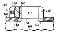
- a first dielectric extension spacer film 124is formed over gate electrode 116 .
- the first extension spacer film 124may be a low-K dielectric having a dielectric constant K of less than approximately 4.0.
- the first extension spacer film 124includes a film of chemically vapor deposited (CVD) silicon nitride.
- the CVD silicon nitridemay be formed by the reaction of dichlorosilane or silane with ammonia in a reactor maintained at a temperature within the range of 300-800° C.
- a CVD silicon oxide pad layermay be deposited over gate electrode 116 prior to depositing the silicon nitride so as to alleviate the stress that often occurs when silicon nitride contacts silicon.
- the first extension spacer film 124is deposited in a substantially conformal manner such that the film thickness in vertical portions of the topography is roughly within at least 80% of the film thickness in horizontal portions of the topography.
- a layer of photoresist 126is then deposited over first extension spacer film 124 such that a portion of the first extension spacer film 124 on one side of the gate electrode 116 is left exposed.
- the exposed portion of the first extension spacer film 124is subsequently removed using a suitable etching technique, and the photoresist is then stripped, after which a second extension spacer film 128 is deposited over the exposed portion of the structure as shown in FIG. 7 .
- the second extension spacer film 128is anisotropically etched to remove a portion thereof. Referring to FIG.
- first and second extension spacer films 124 and 128are then anisotropically etched to produce first and second extension spacer structures 146 and 150 , respectively.
- the etch ratescan be adjusted as necessary to ensure that the extension spacers structures 146 and 150 remain on both sides of the gate electrode 116 .
- the lateral thickness of extension spacer structures 146 and 150is approximately 1 ⁇ 4 to 1 ⁇ 2 the lateral dimension (L) of gate electrode 116 . If, for example, L is approximately 100 nm, then the lateral thickness of extension spacer structures 146 and 150 will typically be within the range of about 25 to about 50 nm, together or individually. In other embodiments, however, the lateral dimensions of extension spacer structures 146 and 150 may be outside of this range. Extension spacer structures 146 and 150 may include CVD silicon oxide, silicon nitride, or a combination of the two. The extension spacer structures 146 and 150 act to prevent shorting between source/drain regions and the gate electrode of the resulting transistor.
- a source/drain implant 154is then performed to introduce source/drain regions 156 in the form of impurity distributions in the substrate 102 .
- the source/drain regions 156are formed using gate electrode 116 and extension spacer structures 146 and 150 as implant masks such that the source/drain regions 156 that result are effectively self-aligned to extension spacer structures 146 and 150 .
- the source/drain implant 154typically uses an n-type species such as phosphorous or arsenic, while in a p-channel transistor embodiment, the source/drain implant 154 typically uses boron or another p-type dopant.
- the impurity distribution in the source/drain region 156is preferably in excess of roughly 10 19 atoms/cm 3 .
- the source and drain regions 156 and the gate electrode 116are subjected to silicidation.
- a metal 166such as cobalt is uniformly deposited over wafer 100 .
- any dielectric materials over the source/drain regions 156including the portion of gate dielectric 104 , and any residual dielectric materials on the upper surface of gate electrode 116 , are removed to expose the doped semiconductor within substrate 102 and the polysilicon or other material of gate electrode 116 .
- the dielectrics to be removedinclude silicon oxide, an HF dip or other suitable wet or dry process may be used for this purpose, while silicon nitride and other dielectrics may require conventional dry etch processing for their removal.
- metal 166is deposited, wafer 100 and metal 166 are exposed to a heated atmosphere to form silicide wherever the metal 166 contacts silicon (or contacts other semiconductor materials).
- a top view of the resulting structureis shown in FIG. 12 .
- the source and drain of the transistorcan be assigned on either side of the first or second extension spacer structures 146 and 150 , respectively.
- Metal 166may include other metals in addition to or in lieu of cobalt, such as nickel, titanium, titanium nitride, and combinations thereof.
- FIGS. 13-16depict another possible embodiment of the methodology described herein.
- anisotropic etchingis utilized to remove portions of first extension spacer film 124 , thus forming the structure depicted in FIG. 13 wherein extension spacer structures 146 are formed on either side of the gate electrode 116 .
- a photoresist mask 148is then utilized to remove the extension spacer structure on one side of the gate electrode 116 , as depicted in FIG. 14 .
- the photoresist mask 148is then stripped, and a second extension spacer film 128 comprising a second dielectric material is deposited over the structure, as shown in FIG. 15 .
- extension spacer film 128is depicted as being thinner than first extension spacer film 124 (see FIG. 4 ).
- the resulting structureis then subjected to an anisotropic etch, thus yielding the structure depicted in FIG. 16 in which extension spacers 146 and 150 are formed which comprise diverse materials and have different dimensions.
- the structure depicted in FIG. 16contains two anisotropic features (the diverse composition and dimensions of the extension spacer structures).
- Source/drain regions 156are then implanted as shown in FIG. 17 , followed by a metal silicidation process of the type previously described that is used to define metal silicide portions 166 over the gate electrode 116 and the source/drain regions 156 .
- this methodresults in the formation on one side of the structure of a layer of SiGe 162 which is disposed between the extension spacer structure 150 and the source/drain extension region 118 .
- the layer of semiconductor material 162is disposed on the source side, such a structure increases injection efficiency without degrading leakage current, because the gate/drain interface is devoid of the semiconductor material.
- SiGeis the preferred material, SiGeC or other suitable semiconductor materials could also be used.
- FIGS. 11 and 17are particularly desirable, because they allow the materials for the extension spacer structures to be selected for the source and drain regions independently of each other.
- the structures of FIGS. 11 and 17can be used to provide nonlinear stress in the channel, and hence allow more options in tuning the stress across the channel in a complimentary manner between the NMOS and PMOS regions.
- this approachallows the extension spacer structures to be formed with different dimensions (e.g., the extension spacer structure on the source side can be made wider than the extension spacer structure on the drain side, or vice versa). Since the width of the extension spacer structures determines the distance between the gate electrode and the source and drain regions, this capability can be used to modify the electrical characteristics of the transistor.
- FIGS. 18 and 19a further embodiment of the methodology disclosed herein is illustrated.
- the exposed portions of the substrate and the exposed side of the gate electrode 116are subjected to thermal oxidation to define a layer of oxide 160 on these surfaces.
- the thermal oxidationmay be accomplished using, for example, an atmosphere comprising a mixture of nitrogen with O 2 or H 2 O.
- a second extension spacer structure 150is then defined over the oxide layer 160 .
- This second extension spacer structure 150may comprise the same or different materials as the first extension spacer structure 146 .
- FIG. 20a further embodiment of the methodology disclosed herein is illustrated.
- all three of the aforementioned asymmetric propertiesare combined into a single structure.
- the exposed portions of the substrateare subjected to epitaxial growth using SiGe, thus resulting in the formation of a source/drain extension layer 162 thereon.
- a third extension spacer structure 152is then defined over the source/drain extension layer 162 as shown in FIG. 21 .
- This third extension spacer structure 152may comprise the same or different materials as the first extension spacer structure 146 and the second extension spacer structyure 150 .
- This approachcan be utilized to form structures with particularly desirable properties.
- this approachcan be used for the selective formation of a thicker layer of oxide 160 on the drain side than on the source side.
- Such an approachpermits the electrical properties of the transistor to be tuned as desired.
- this approachcan be utilized to reduce capacitance and leakage current of the transistor on the drain side, without adversely effecting the source side. This approach is possible since the drain side is where the transistor is biased with a higher potential, and hence is prone to higher electric fields which induce leakage. This approach also improves the reliability of the transistor structure.
Landscapes
- Insulated Gate Type Field-Effect Transistor (AREA)
- Thin Film Transistor (AREA)
Abstract
Description
- The present disclosure relates generally to the fabrication of semiconductor devices, and relates more particularly to methods for forming transistors having asymmetric extension spacers or asymmetric source/drain extension layers.
- Ideally, transistors should exhibit both high performance and low power consumption. Typically, however, the design and fabrication of transistors has required a tradeoff between these two parameters. In particular, in conventional processes, optimizing one of these parameters tends to adversely affect the other. For example, as transistor channel lengths are decreased to improve the speed of a device, thereby optimizing device performance, other characteristics, such as sub-threshold leakage, tend to become more difficult to control, thereby increasing the power consumption of the device.
- There is thus a need in the art for a transistor, and a method for making the same, which overcomes this infirmity. In particular, there is a need in the art for a transistor, and a method for making the same, in which aspects of the device which affect performance characteristics can be optimized independently of those aspects which minimize power consumption. These and other needs are met by the devices and methodologies described herein.
- In one aspect, a method of forming a semiconductor device, such as a transistor, is provided. In accordance with the method, a substrate is provided which has a gate dielectric layer disposed thereon. A gate electrode is formed over the gate dielectric layer, the gate electrode having first and second sidewalls. First and second extension spacer structures are formed adjacent the first and second sidewalls, respectively. The semiconductor device has at least one characteristic selected from the group consisting of: (a) the first and second extension spacer structures have different dimensions; (b) the first and second extension spacer structures comprise first and second distinct materials; (c) the device has source/drain extensions that are asymmetrically disposed about the gate electrode; and (d) the device has a first dielectric layer disposed between the first extension spacer structure and the gate electrode, and either (i) the device has no dielectric layer disposed between the second extension spacer structure and the gate electrode, or (ii) the device has a second dielectric layer disposed between the second extension spacer structure and the gate electrode, and the first dielectric layer is substantially thicker than the second dielectric layer.
- In another aspect, a semiconductor device, such as a transistor, is provided. The semiconductor device comprises (a) a substrate having a gate dielectric layer disposed thereon, (b) a gate electrode disposed over the gate dielectric layer, the gate electrode having first and second sidewalls, and (c) first and second extension spacer structures adjacent said first and second sidewalls, respectively; wherein the semiconductor device has at least one characteristic selected from the group consisting of: (a) the first and second extension spacer structures have different dimensions; (b) the first and second extension spacer structures comprise first and second distinct materials; (c) the device has source/drain extensions that are asymmetrically disposed about the gate electrode; and (d) the device has a first dielectric layer disposed between the first extension spacer structure and the gate electrode, and either (i) the device has no dielectric layer disposed between the second extension spacer structure and the gate electrode, or (ii) the device has a second dielectric layer disposed between the second extension spacer structure and the gate electrode, and the first dielectric layer is substantially thicker than the second dielectric layer. These and other aspects of the present disclosure are described in greater detail below.
FIG. 1 is a partial cross-sectional view of a semiconductor wafer in which a gate dielectric is formed over a semiconductor substrate;FIG. 2 illustrates processing subsequent toFIG. 1 in which a gate electrode film is formed over the gate dielectric;FIG. 3 illustrates processing subsequent toFIG. 2 in which the gate electrode film is patterned to form a gate electrode structure;FIG. 4 illustrates processing subsequent toFIG. 3 in which a first dielectric is formed over the substrate and the gate electrode;FIG. 5 illustrates processing subsequent toFIG. 4 in which a photoresist mask is formed over the first dielectric layer;FIG. 6 illustrates processing subsequent toFIG. 5 in which a portion of the first dielectric film is removed;FIG. 7 illustrates processing subsequent toFIG. 6 in which the photoresist is removed and a second dielectric film is formed on the exposed portion of the substrate;FIG. 8 illustrates processing subsequent toFIG. 7 in which a first sidewall spacer is formed;FIG. 9 illustrates processing subsequent toFIG. 8 in which the first and second dielectric films are etched to form the dielectric spacers;FIG. 10 illustrates processing subsequent toFIG. 9 in which source/drain regions of the substrate are implanted using the gate electrode, the extensions, and the dielectrics as an implant mask;FIG. 11 illustrates processing subsequent toFIG. 10 in which a metal film is deposited over the wafer and in which silicide regions are formed;FIG. 12 is a top view of a transistor made by the process depicted inFIGS. 1-11 ;FIG. 13 illustrates processing subsequent toFIG. 4 in which the first dielectric layer has been etched to form dielectric spacers;FIG. 14 illustrates processing subsequent toFIG. 13 in which a photoresist mask has been deposited over the structure, followed by etching to remove one of the spacer structures;FIG. 15 illustrates processing subsequent toFIG. 14 in which the photoresist mask has been stripped, followed by deposition of a second dielectric layer that is thinner and of a different material than the first dielectric layer;FIG. 16 illustrates processing subsequent toFIG. 15 in which the first and second dielectric layer has been etched to form first and second dielectric spacers;FIG. 17 illustrates processing subsequent toFIG. 16 in which a selective epitaxy is used to grow extension layers in exposed regions of the device;FIG. 18 illustrates processing subsequent toFIG. 14 in which the photoresist mask is stripped, followed by oxidation of the exposed surfaces;FIG. 19 illustrates processing subsequent toFIG. 18 in which a second dielectric film is deposited over the wafer, and a second spacer is formed;FIG. 20 illustrates processing subsequent toFIG. 14 in which silicon regions in the source and drain regions are exposed and SiGe is epitaxially grown on the exposed surfaces; andFIG. 21 illustrates processing subsequent toFIG. 20 in which a third spacer structure is formed by deposition of a second dielectric layer, followed by etching (this figure illustrates three asymmetries, including asymmetric spacers, asymmetric source/drain layers under spacers, and asymmetric re-oxidized layers).- It has now been found that the aforementioned needs may be met by forming a transistor or other semiconductor device by providing a substrate having a gate dielectric layer disposed thereon; forming a gate electrode over the gate dielectric layer, the gate electrode having first and second sidewalls; and forming first and second extension spacers adjacent to the first and second sidewalls, respectively. In some embodiments, various other steps may be performed, such as the formation of source/drain regions and/or source/drain extension, and the formation of dielectric layers between one or both of the first and second extension spacers. These steps are conducted such that the semiconductor device has at least one characteristic selected from the group consisting of: (a) the first and second spacers have different dimensions; (b) the first and second spacers comprise first and second distinct materials; (c) the device has source/drain extensions that are asymmetrically disposed about the gate electrode; and (d) the device has a first dielectric layer disposed between the first spacer and the gate electrode, and either (i) the device has no dielectric layer disposed between the second spacer and the gate electrode, or (ii) the device has a second dielectric layer disposed between the second spacer and the gate electrode, and the first dielectric layer is substantially thicker than the second dielectric layer.
- The methodology described herein permits the formation of asymmetric spacers and/or asymmetric source/drain layers that have a variety of useful properties, and also permits the spacers and/or source/drain layers to be formed and defined independently of each other, to be formed out of different materials, and to be created with different dimensions.
- For example, this approach permits the formation of a thicker oxide layer at the drain side of a transistor (which reduces leakage) without a corresponding increase in the thickness of the oxide layer (and associated reduction in gate capacitance) at the source side of the transistor, where the oxide layer is preferably as thin as possible. This approach also permits the formation of structures in which the first and second spacers comprise diverse materials (e.g., one spacer comprises oxide and the other spacer comprises nitride); such structures provide nonlinear stress in the channel, and hence provide more options in tuning the stress across the channel in a complimentary manner between NMOS and PMOS regions of CMOS devices. Moreover, the use of asymmetric portions of SiGe in the extension regions provides more options in choosing between NMOS/PMOS and Ion/Iofftrade off; thus, for example, complimentary NMOS/PMOS devices can trade off Ion/Ioff, depending on which side is wired as the source or drain.
- Generally speaking, the teachings herein contemplate the formation of a transistor that employs (preferably dielectric) extension spacer structures on the sidewalls of the transistor gate electrode. Specific embodiments of the processes that may be used to form these structures are disclosed herein, it being understood that many variations in these processes are possible without departing from the scope of the present teachings.
- Referring now to
FIG. 1 , a gatedielectric film 104 is formed over asemiconductor substrate 102 of asemiconductor wafer 100. In one embodiment, gate dielectric104 is a silicon dioxide film formed by the thermal oxidation of the upper surface ofsemiconductor substrate 102. Thermal oxidation ofsubstrate 102 may be achieved, for example, by exposing the wafer to an oxidizing atmosphere (e.g., O2, H2O, or the like) at a temperature in excess of 900° C. - Typically, gate dielectric104 has a thickness of anywhere from about 15 to about 150 angstroms. In some embodiments, the gate dielectric104 may be a “high K” dielectric having a dielectric constant K which is greater than 4.0. High K dielectrics are desirable for use in gate dielectric films to achieve sufficient capacitance with a thicker film. High K materials suitable for use as the gate dielectric104 include various metal-oxide compounds such as hafnium-oxide, as well as other materials including aluminum oxide, hafnium silicate, zirconium silicate, hafnium aluminate, lanthanum aluminate, zirconium aluminate, and lanthanum oxide.
- The upper portion of
semiconductor substrate 102 typically includes a monocrystalline semiconductor material such as silicon on which the gate dielectric104 is formed. In one embodiment that is particularly suitable for use with low power applications such as mobile and wireless devices,semiconductor substrate 102 is a silicon-on-insulator (SOI) substrate in which the monocrystalline silicon is a relatively thin film (i.e., less than 10,000 angstroms) formed over a buried oxide with a thickness roughly in the range of 1000 to 20,000 angstroms. - Referring now to
FIG. 2 , agate electrode film 106 is formed over the gate dielectric104. Preferably,gate electrode film 106 is a polysilicon film which may be formed by the thermal decomposition of silane in a reactor chamber maintained at a temperature in the range of approximately 550-650° C. When thegate electrode film 106 is polysilicon, the polysilicon film is typically deposited as undoped silicon and is subsequently doped with an n-type (e.g., phosphorous, arsenic) or p-type (e.g., boron) dopant using ion implantation. The polysilicon may be doped in-situ or by diffusion. In some embodiments, thegate electrode film 106 may also comprise such materials as germanium, tantalum silicon nitride, titanium nitride, molybdenum nitride or a combination thereof, either in addition to or in lieu of polysilicon. - Referring now to
FIG. 3 , gate electrode film106 (seeFIG. 2 ) is patterned to form agate electrode 116 having substantiallyvertical sidewalls 112.Gate electrode 116 is typically patterned using photolithography and anisotropic or dry etch techniques that are well known in the art. The photolithography may include the use of an anti-reflective coating (ARC) and photoresist patterning techniques. - Referring now to
FIG. 4 , one or more implant steps may be performed after forminggate electrode 116. In some embodiments, one or more implants are formed to introduce source/drain extension regions 118 into those portions ofsubstrate 102 not covered bygate electrode 116. The source/drain extension regions 118 are desirable to control the threshold voltage and effective channel-length of the resulting device. In embodiments in which thesubstrate 102 is an SOI wafer, however, high dose ion implantation is undesirable because it is difficult to maintain the dose adequately within the very shallow silicon substrate. - Referring again to
FIG. 4 , a first dielectricextension spacer film 124 is formed overgate electrode 116. In some embodiments, the firstextension spacer film 124 may be a low-K dielectric having a dielectric constant K of less than approximately 4.0. In other embodiments, the firstextension spacer film 124 includes a film of chemically vapor deposited (CVD) silicon nitride. In such later embodiments, the CVD silicon nitride may be formed by the reaction of dichlorosilane or silane with ammonia in a reactor maintained at a temperature within the range of 300-800° C. A CVD silicon oxide pad layer may be deposited overgate electrode 116 prior to depositing the silicon nitride so as to alleviate the stress that often occurs when silicon nitride contacts silicon. The firstextension spacer film 124 is deposited in a substantially conformal manner such that the film thickness in vertical portions of the topography is roughly within at least 80% of the film thickness in horizontal portions of the topography. - As shown in
FIG. 5 , a layer ofphotoresist 126 is then deposited over firstextension spacer film 124 such that a portion of the firstextension spacer film 124 on one side of thegate electrode 116 is left exposed. As shown inFIG. 6 , the exposed portion of the firstextension spacer film 124 is subsequently removed using a suitable etching technique, and the photoresist is then stripped, after which a secondextension spacer film 128 is deposited over the exposed portion of the structure as shown inFIG. 7 . Then, as shown inFIG. 8 , the secondextension spacer film 128 is anisotropically etched to remove a portion thereof. Referring toFIG. 9 , a portion of the first and secondextension spacer films extension spacer structures extension spacers structures gate electrode 116. - Preferably, the lateral thickness of
extension spacer structures gate electrode 116. If, for example, L is approximately 100 nm, then the lateral thickness ofextension spacer structures extension spacer structures Extension spacer structures extension spacer structures - Referring now to
FIG. 10 , a source/drain implant 154 is then performed to introduce source/drain regions 156 in the form of impurity distributions in thesubstrate 102. The source/drain regions 156 are formed usinggate electrode 116 andextension spacer structures drain regions 156 that result are effectively self-aligned toextension spacer structures drain implant 154 typically uses an n-type species such as phosphorous or arsenic, while in a p-channel transistor embodiment, the source/drain implant 154 typically uses boron or another p-type dopant. The impurity distribution in the source/drain region 156 is preferably in excess of roughly 1019atoms/cm3. - Referring now to
FIG. 11 , the source and drainregions 156 and thegate electrode 116 are subjected to silicidation. In particular, ametal 166 such as cobalt is uniformly deposited overwafer 100. Prior to this deposition, any dielectric materials over the source/drain regions 156, including the portion ofgate dielectric 104, and any residual dielectric materials on the upper surface ofgate electrode 116, are removed to expose the doped semiconductor withinsubstrate 102 and the polysilicon or other material ofgate electrode 116. To the extent that the dielectrics to be removed include silicon oxide, an HF dip or other suitable wet or dry process may be used for this purpose, while silicon nitride and other dielectrics may require conventional dry etch processing for their removal. - After
metal 166 is deposited,wafer 100 andmetal 166 are exposed to a heated atmosphere to form silicide wherever themetal 166 contacts silicon (or contacts other semiconductor materials). The portions ofmetal 166 in contact with a dielectric, including those in contact withspacer extension structures FIG. 11 . A top view of the resulting structure is shown inFIG. 12 . As shown inFIG. 12 , the source and drain of the transistor can be assigned on either side of the first or secondextension spacer structures Metal 166 may include other metals in addition to or in lieu of cobalt, such as nickel, titanium, titanium nitride, and combinations thereof. FIGS. 13-16 depict another possible embodiment of the methodology described herein. Starting with the structure depicted inFIG. 4 , anisotropic etching is utilized to remove portions of firstextension spacer film 124, thus forming the structure depicted inFIG. 13 whereinextension spacer structures 146 are formed on either side of thegate electrode 116. Aphotoresist mask 148 is then utilized to remove the extension spacer structure on one side of thegate electrode 116, as depicted inFIG. 14 . Thephotoresist mask 148 is then stripped, and a secondextension spacer film 128 comprising a second dielectric material is deposited over the structure, as shown inFIG. 15 . In this case,extension spacer film 128 is depicted as being thinner than first extension spacer film124 (seeFIG. 4 ). The resulting structure is then subjected to an anisotropic etch, thus yielding the structure depicted inFIG. 16 in whichextension spacers FIG. 16 contains two anisotropic features (the diverse composition and dimensions of the extension spacer structures).- Source/
drain regions 156 are then implanted as shown inFIG. 17 , followed by a metal silicidation process of the type previously described that is used to definemetal silicide portions 166 over thegate electrode 116 and the source/drain regions 156. As shown inFIG. 17 , this method results in the formation on one side of the structure of a layer ofSiGe 162 which is disposed between theextension spacer structure 150 and the source/drain extension region 118. Assuming that the layer ofsemiconductor material 162 is disposed on the source side, such a structure increases injection efficiency without degrading leakage current, because the gate/drain interface is devoid of the semiconductor material. It will be appreciated that, while SiGe is the preferred material, SiGeC or other suitable semiconductor materials could also be used. - The structures depicted in
FIGS. 11 and 17 are particularly desirable, because they allow the materials for the extension spacer structures to be selected for the source and drain regions independently of each other. The structures ofFIGS. 11 and 17 can be used to provide nonlinear stress in the channel, and hence allow more options in tuning the stress across the channel in a complimentary manner between the NMOS and PMOS regions. Moreover, this approach allows the extension spacer structures to be formed with different dimensions (e.g., the extension spacer structure on the source side can be made wider than the extension spacer structure on the drain side, or vice versa). Since the width of the extension spacer structures determines the distance between the gate electrode and the source and drain regions, this capability can be used to modify the electrical characteristics of the transistor. - With reference to
FIGS. 18 and 19 , a further embodiment of the methodology disclosed herein is illustrated. Starting with a structure similar to that depicted inFIG. 14 (but in which the mask is disposed only over the top of the gate electrode116), the exposed portions of the substrate and the exposed side of thegate electrode 116 are subjected to thermal oxidation to define a layer ofoxide 160 on these surfaces. The thermal oxidation may be accomplished using, for example, an atmosphere comprising a mixture of nitrogen with O2or H2O. Using the methodologies previously described, a secondextension spacer structure 150 is then defined over theoxide layer 160. This secondextension spacer structure 150 may comprise the same or different materials as the firstextension spacer structure 146. - Referring now to
FIG. 20 , a further embodiment of the methodology disclosed herein is illustrated. In this case, all three of the aforementioned asymmetric properties are combined into a single structure. Starting with the structure depicted inFIG. 19 , the exposed portions of the substrate are subjected to epitaxial growth using SiGe, thus resulting in the formation of a source/drain extension layer 162 thereon. Using the methodologies previously described, a thirdextension spacer structure 152 is then defined over the source/drain extension layer 162 as shown inFIG. 21 . This thirdextension spacer structure 152 may comprise the same or different materials as the firstextension spacer structure 146 and the secondextension spacer structyure 150. - This approach can be utilized to form structures with particularly desirable properties. In particular, if the
extension spacer structure 146 is positioned on the source side, this approach can be used for the selective formation of a thicker layer ofoxide 160 on the drain side than on the source side. Such an approach permits the electrical properties of the transistor to be tuned as desired. For example, this approach can be utilized to reduce capacitance and leakage current of the transistor on the drain side, without adversely effecting the source side. This approach is possible since the drain side is where the transistor is biased with a higher potential, and hence is prone to higher electric fields which induce leakage. This approach also improves the reliability of the transistor structure. - The above description of the present invention is illustrative, and is not intended to be limiting. It will thus be appreciated that various additions, substitutions and modifications may be made to the above described embodiments without departing from the scope of the present invention. Accordingly, the scope of the present invention should be construed in reference to the appended claims.
Claims (23)
Priority Applications (1)
| Application Number | Priority Date | Filing Date | Title |
|---|---|---|---|
| US11/047,946US7585735B2 (en) | 2005-02-01 | 2005-02-01 | Asymmetric spacers and asymmetric source/drain extension layers |
Applications Claiming Priority (1)
| Application Number | Priority Date | Filing Date | Title |
|---|---|---|---|
| US11/047,946US7585735B2 (en) | 2005-02-01 | 2005-02-01 | Asymmetric spacers and asymmetric source/drain extension layers |
Publications (2)
| Publication Number | Publication Date |
|---|---|
| US20060170016A1true US20060170016A1 (en) | 2006-08-03 |
| US7585735B2 US7585735B2 (en) | 2009-09-08 |
Family
ID=36755596
Family Applications (1)
| Application Number | Title | Priority Date | Filing Date |
|---|---|---|---|
| US11/047,946Active2026-02-24US7585735B2 (en) | 2005-02-01 | 2005-02-01 | Asymmetric spacers and asymmetric source/drain extension layers |
Country Status (1)
| Country | Link |
|---|---|
| US (1) | US7585735B2 (en) |
Cited By (14)
| Publication number | Priority date | Publication date | Assignee | Title |
|---|---|---|---|---|
| US20060017103A1 (en)* | 2004-06-07 | 2006-01-26 | Stmicroelectronics Sa | Method for making reduced size DMOS transistor and resulting DMOS transistor |
| US20070145430A1 (en)* | 2005-12-22 | 2007-06-28 | Micron Technology, Inc. | CMOS device with asymmetric gate strain |
| US20080157199A1 (en)* | 2006-12-27 | 2008-07-03 | Spansion Llc | Dielectric extension to mitigate short channel effects |
| US20090039388A1 (en)* | 2007-08-07 | 2009-02-12 | Chartered Semiconductor Manufacturing Ltd. | Integrated circuit system employing a condensation process |
| US20110049582A1 (en)* | 2009-09-03 | 2011-03-03 | International Business Machines Corporation | Asymmetric source and drain stressor regions |
| CN102544106A (en)* | 2012-02-20 | 2012-07-04 | 电子科技大学 | Lateral double-diffusion metal oxide semiconductor (LDMOS) device introducing local stress |
| US20120273853A1 (en)* | 2009-09-09 | 2012-11-01 | Fujitsu Semiconductor Limited | Semiconductor device and method of manufacturing same |
| US20140291761A1 (en)* | 2013-03-29 | 2014-10-02 | International Business Machines Corporation | Asymmetric Spacers |
| US20140295674A1 (en)* | 2013-03-29 | 2014-10-02 | International Business Machines Corporation | Angled gas cluster ion beam |
| CN104425594A (en)* | 2013-08-20 | 2015-03-18 | 中芯国际集成电路制造(上海)有限公司 | Fin field effect transistor and forming method thereof |
| US10079290B2 (en)* | 2016-12-30 | 2018-09-18 | United Microelectronics Corp. | Semiconductor device having asymmetric spacer structures |
| KR20200113130A (en)* | 2019-03-22 | 2020-10-06 | 삼성전자주식회사 | Semiconductor device |
| CN113659077A (en)* | 2020-05-12 | 2021-11-16 | 北京元芯碳基集成电路研究院 | Semiconductor transistor and preparation method thereof |
| EP4036989A1 (en)* | 2021-01-28 | 2022-08-03 | MediaTek Inc. | Semiconductor device and method of forming the same |
Families Citing this family (10)
| Publication number | Priority date | Publication date | Assignee | Title |
|---|---|---|---|---|
| US7892928B2 (en)* | 2007-03-23 | 2011-02-22 | International Business Machines Corporation | Method of forming asymmetric spacers and methods of fabricating semiconductor device using asymmetric spacers |
| JP5280121B2 (en)* | 2008-07-07 | 2013-09-04 | ルネサスエレクトロニクス株式会社 | Semiconductor device and manufacturing method thereof |
| US8237197B2 (en) | 2010-07-07 | 2012-08-07 | International Business Machines Corporation | Asymmetric channel MOSFET |
| US8030154B1 (en)* | 2010-08-03 | 2011-10-04 | International Business Machines Corporation | Method for forming a protection layer over metal semiconductor contact and structure formed thereon |
| US8193099B1 (en) | 2011-03-17 | 2012-06-05 | International Business Machines Corporation | Protecting exposed metal gate structures from etching processes in integrated circuit manufacturing |
| US9412667B2 (en) | 2014-11-25 | 2016-08-09 | International Business Machines Corporation | Asymmetric high-k dielectric for reducing gate induced drain leakage |
| US10134859B1 (en) | 2017-11-09 | 2018-11-20 | International Business Machines Corporation | Transistor with asymmetric spacers |
| US10833165B2 (en) | 2018-04-30 | 2020-11-10 | International Business Machines Corporation | Asymmetric air spacer gate-controlled device with reduced parasitic capacitance |
| US10236364B1 (en) | 2018-06-22 | 2019-03-19 | International Busines Machines Corporation | Tunnel transistor |
| US10249755B1 (en) | 2018-06-22 | 2019-04-02 | International Business Machines Corporation | Transistor with asymmetric source/drain overlap |
Citations (15)
| Publication number | Priority date | Publication date | Assignee | Title |
|---|---|---|---|---|
| US5656518A (en)* | 1996-09-13 | 1997-08-12 | Advanced Micro Devices, Inc. | Method for fabrication of a non-symmetrical transistor |
| US5952702A (en)* | 1996-11-04 | 1999-09-14 | Advanced Micro Devices, Inc. | High performance MOSFET structure having asymmetrical spacer formation and having source and drain regions with different doping concentration |
| US6004849A (en)* | 1997-08-15 | 1999-12-21 | Advanced Micro Devices, Inc. | Method of making an asymmetrical IGFET with a silicide contact on the drain without a silicide contact on the source |
| US6150266A (en)* | 1999-01-28 | 2000-11-21 | Vlsi Technology, Inc. | Local interconnect formed using silicon spacer |
| US6200864B1 (en)* | 1999-06-23 | 2001-03-13 | Advanced Micro Devices, Inc. | Method of asymmetrically doping a region beneath a gate |
| US6246091B1 (en)* | 1997-12-05 | 2001-06-12 | Texas Instruments Incorporated | Lateral MOSFET having a barrier between the source/drain regions and the channel |
| US6255219B1 (en)* | 1999-09-07 | 2001-07-03 | Advanced Micro Devices, Inc. | Method for fabricating high-performance submicron MOSFET with lateral asymmetric channel |
| US6344396B1 (en)* | 1999-09-24 | 2002-02-05 | Advanced Micro Devices, Inc. | Removable spacer technology using ion implantation for forming asymmetric MOS transistors |
| US20040075151A1 (en)* | 2002-10-21 | 2004-04-22 | International Business Machines Corporation | Semiconductor device structure including multiple fets having different spacer widths |
| US6746924B1 (en)* | 2003-02-27 | 2004-06-08 | International Business Machines Corporation | Method of forming asymmetric extension mosfet using a drain side spacer |
| US20040217392A1 (en)* | 2003-04-30 | 2004-11-04 | Leo Mathew | Semiconductor fabrication process with asymmetrical conductive spacers |
| US6887762B1 (en)* | 1998-11-12 | 2005-05-03 | Intel Corporation | Method of fabricating a field effect transistor structure with abrupt source/drain junctions |
| US20060121711A1 (en)* | 2004-12-03 | 2006-06-08 | Advanced Micro Devices, Inc. | Method for forming a semiconductor arrangement with gate sidewall spacers of specific dimensions |
| US7183662B2 (en)* | 2003-08-23 | 2007-02-27 | Samsung Electronics Co., Ltd. | Memory devices with memory cell transistors having gate sidewell spacers with different dielectric properties |
| US20080142838A1 (en)* | 2006-12-13 | 2008-06-19 | Fujitsu Limited | Semiconductor device and method of manufacturing semiconductor device |
- 2005
- 2005-02-01USUS11/047,946patent/US7585735B2/enactiveActive
Patent Citations (15)
| Publication number | Priority date | Publication date | Assignee | Title |
|---|---|---|---|---|
| US5656518A (en)* | 1996-09-13 | 1997-08-12 | Advanced Micro Devices, Inc. | Method for fabrication of a non-symmetrical transistor |
| US5952702A (en)* | 1996-11-04 | 1999-09-14 | Advanced Micro Devices, Inc. | High performance MOSFET structure having asymmetrical spacer formation and having source and drain regions with different doping concentration |
| US6004849A (en)* | 1997-08-15 | 1999-12-21 | Advanced Micro Devices, Inc. | Method of making an asymmetrical IGFET with a silicide contact on the drain without a silicide contact on the source |
| US6246091B1 (en)* | 1997-12-05 | 2001-06-12 | Texas Instruments Incorporated | Lateral MOSFET having a barrier between the source/drain regions and the channel |
| US6887762B1 (en)* | 1998-11-12 | 2005-05-03 | Intel Corporation | Method of fabricating a field effect transistor structure with abrupt source/drain junctions |
| US6150266A (en)* | 1999-01-28 | 2000-11-21 | Vlsi Technology, Inc. | Local interconnect formed using silicon spacer |
| US6200864B1 (en)* | 1999-06-23 | 2001-03-13 | Advanced Micro Devices, Inc. | Method of asymmetrically doping a region beneath a gate |
| US6255219B1 (en)* | 1999-09-07 | 2001-07-03 | Advanced Micro Devices, Inc. | Method for fabricating high-performance submicron MOSFET with lateral asymmetric channel |
| US6344396B1 (en)* | 1999-09-24 | 2002-02-05 | Advanced Micro Devices, Inc. | Removable spacer technology using ion implantation for forming asymmetric MOS transistors |
| US20040075151A1 (en)* | 2002-10-21 | 2004-04-22 | International Business Machines Corporation | Semiconductor device structure including multiple fets having different spacer widths |
| US6746924B1 (en)* | 2003-02-27 | 2004-06-08 | International Business Machines Corporation | Method of forming asymmetric extension mosfet using a drain side spacer |
| US20040217392A1 (en)* | 2003-04-30 | 2004-11-04 | Leo Mathew | Semiconductor fabrication process with asymmetrical conductive spacers |
| US7183662B2 (en)* | 2003-08-23 | 2007-02-27 | Samsung Electronics Co., Ltd. | Memory devices with memory cell transistors having gate sidewell spacers with different dielectric properties |
| US20060121711A1 (en)* | 2004-12-03 | 2006-06-08 | Advanced Micro Devices, Inc. | Method for forming a semiconductor arrangement with gate sidewall spacers of specific dimensions |
| US20080142838A1 (en)* | 2006-12-13 | 2008-06-19 | Fujitsu Limited | Semiconductor device and method of manufacturing semiconductor device |
Cited By (33)
| Publication number | Priority date | Publication date | Assignee | Title |
|---|---|---|---|---|
| US20060017103A1 (en)* | 2004-06-07 | 2006-01-26 | Stmicroelectronics Sa | Method for making reduced size DMOS transistor and resulting DMOS transistor |
| US8093658B2 (en) | 2005-12-22 | 2012-01-10 | Micron Technology, Inc. | Electronic device with asymmetric gate strain |
| US20160268428A1 (en)* | 2005-12-22 | 2016-09-15 | Micron Technology, Inc. | Electronic device with asymmetric gate strain |
| US8803240B2 (en)* | 2005-12-22 | 2014-08-12 | Micron Technology, Inc. | Electronic device with asymmetric gate strain |
| US7656049B2 (en)* | 2005-12-22 | 2010-02-02 | Micron Technology, Inc. | CMOS device with asymmetric gate strain |
| US9356145B2 (en)* | 2005-12-22 | 2016-05-31 | Micron Technology, Inc. | Electronic device with asymmetric gate strain |
| US20100133612A1 (en)* | 2005-12-22 | 2010-06-03 | Sandhu Gurtej S | Electronic device with asymmetric gate strain |
| US9780184B2 (en)* | 2005-12-22 | 2017-10-03 | Micron Technology, Inc. | Electronic device with asymmetric gate strain |
| US20070145430A1 (en)* | 2005-12-22 | 2007-06-28 | Micron Technology, Inc. | CMOS device with asymmetric gate strain |
| US20140346577A1 (en)* | 2005-12-22 | 2014-11-27 | Micron Technology, Inc. | Electronic device with asymmetric gate strain |
| US20120104476A1 (en)* | 2005-12-22 | 2012-05-03 | Sandhu Gurtej S | Electronic device with asymmetric gate strain |
| US20080157199A1 (en)* | 2006-12-27 | 2008-07-03 | Spansion Llc | Dielectric extension to mitigate short channel effects |
| US9318333B2 (en) | 2006-12-27 | 2016-04-19 | Cypress Semiconductor Corporation | Dielectric extension to mitigate short channel effects |
| US7692213B2 (en) | 2007-08-07 | 2010-04-06 | Chartered Semiconductor Manufacturing Ltd. | Integrated circuit system employing a condensation process |
| US20090039388A1 (en)* | 2007-08-07 | 2009-02-12 | Chartered Semiconductor Manufacturing Ltd. | Integrated circuit system employing a condensation process |
| US20110212587A1 (en)* | 2009-09-03 | 2011-09-01 | International Business Machines Corporation | Asymmetric source and drain stressor regions |
| US20110049582A1 (en)* | 2009-09-03 | 2011-03-03 | International Business Machines Corporation | Asymmetric source and drain stressor regions |
| US8193065B2 (en) | 2009-09-03 | 2012-06-05 | International Business Machines Corporation | Asymmetric source and drain stressor regions |
| US20120273853A1 (en)* | 2009-09-09 | 2012-11-01 | Fujitsu Semiconductor Limited | Semiconductor device and method of manufacturing same |
| US9012285B2 (en) | 2009-09-09 | 2015-04-21 | Fujitsu Semiconductor Limited | Semiconductor device and method of manufacturing same |
| CN102544106A (en)* | 2012-02-20 | 2012-07-04 | 电子科技大学 | Lateral double-diffusion metal oxide semiconductor (LDMOS) device introducing local stress |
| US9236447B2 (en) | 2013-03-29 | 2016-01-12 | Globalfoundries Inc. | Asymmetric spacers |
| US20140295674A1 (en)* | 2013-03-29 | 2014-10-02 | International Business Machines Corporation | Angled gas cluster ion beam |
| US20140291761A1 (en)* | 2013-03-29 | 2014-10-02 | International Business Machines Corporation | Asymmetric Spacers |
| CN104425594A (en)* | 2013-08-20 | 2015-03-18 | 中芯国际集成电路制造(上海)有限公司 | Fin field effect transistor and forming method thereof |
| US10079290B2 (en)* | 2016-12-30 | 2018-09-18 | United Microelectronics Corp. | Semiconductor device having asymmetric spacer structures |
| US20180350937A1 (en)* | 2016-12-30 | 2018-12-06 | United Microelectronics Corp. | Method for fabricating a semiconductor device |
| US10510884B2 (en)* | 2016-12-30 | 2019-12-17 | United Microelectronics Corp. | Method for fabricating a semiconductor device |
| KR20200113130A (en)* | 2019-03-22 | 2020-10-06 | 삼성전자주식회사 | Semiconductor device |
| KR102783915B1 (en) | 2019-03-22 | 2025-03-24 | 삼성전자주식회사 | Semiconductor device |
| CN113659077A (en)* | 2020-05-12 | 2021-11-16 | 北京元芯碳基集成电路研究院 | Semiconductor transistor and preparation method thereof |
| EP4036989A1 (en)* | 2021-01-28 | 2022-08-03 | MediaTek Inc. | Semiconductor device and method of forming the same |
| TWI864363B (en)* | 2021-01-28 | 2024-12-01 | 聯發科技股份有限公司 | Semiconductor device and method of forming the same |
Also Published As
| Publication number | Publication date |
|---|---|
| US7585735B2 (en) | 2009-09-08 |
Similar Documents
| Publication | Publication Date | Title |
|---|---|---|
| US7585735B2 (en) | Asymmetric spacers and asymmetric source/drain extension layers | |
| US7781290B2 (en) | Complementary metal-oxide semiconductor (CMOS) devices including a thin-body channel and dual gate dielectric layers and methods of manufacturing the same | |
| US6967143B2 (en) | Semiconductor fabrication process with asymmetrical conductive spacers | |
| US8871584B2 (en) | Replacement source/drain finFET fabrication | |
| US6707062B2 (en) | Transistor in a semiconductor device with an elevated channel and a source drain | |
| EP1478029B1 (en) | Method of fabricating a MOS transistor | |
| US7867860B2 (en) | Strained channel transistor formation | |
| CN102290374B (en) | Method of manufacturing integrated circuit device | |
| US6686245B1 (en) | Vertical MOSFET with asymmetric gate structure | |
| KR100551417B1 (en) | Cmos device structure with improved pfet gate electrode | |
| US7763510B1 (en) | Method for PFET enhancement | |
| US20080217665A1 (en) | Semiconductor device structure having enhanced performance fet device | |
| US20130122675A1 (en) | Method for fabricating a semiconductor device | |
| CN102165571A (en) | Method for fabricating MOS devices with highly stressed channels | |
| US6696328B2 (en) | CMOS gate electrode using selective growth and a fabrication method thereof | |
| US20100081246A1 (en) | Method of manufacturing a semiconductor | |
| US7645687B2 (en) | Method to fabricate variable work function gates for FUSI devices | |
| US7776695B2 (en) | Semiconductor device structure having low and high performance devices of same conductive type on same substrate | |
| US9331174B2 (en) | Method for improving device performance using epitaxially grown silicon carbon (SiC) or silicon-germanium (SiGe) | |
| US7910422B2 (en) | Reducing gate CD bias in CMOS processing | |
| US7820539B2 (en) | Method for separately optimizing spacer width for two transistor groups using a recess spacer etch (RSE) integration | |
| US20050136580A1 (en) | Hydrogen free formation of gate electrodes | |
| US7902021B2 (en) | Method for separately optimizing spacer width for two or more transistor classes using a recess spacer integration | |
| JP3518059B2 (en) | Method of manufacturing MIS transistor | |
| WO2009084376A1 (en) | Semiconductor device and process for producing the semiconductor device |
Legal Events
| Date | Code | Title | Description |
|---|---|---|---|
| AS | Assignment | Owner name:FREESCALE SEMICONDUCTOR, INC., ILLINOIS Free format text:ASSIGNMENT OF ASSIGNORS INTEREST;ASSIGNORS:MATTHEW, LEO;DU, YANG;NGUYEN, BICH-YEN;AND OTHERS;REEL/FRAME:016310/0164;SIGNING DATES FROM 20050131 TO 20050202 | |
| AS | Assignment | Owner name:CITIBANK, N.A. AS COLLATERAL AGENT, NEW YORK Free format text:SECURITY AGREEMENT;ASSIGNORS:FREESCALE SEMICONDUCTOR, INC.;FREESCALE ACQUISITION CORPORATION;FREESCALE ACQUISITION HOLDINGS CORP.;AND OTHERS;REEL/FRAME:018855/0129 Effective date:20061201 Owner name:CITIBANK, N.A. AS COLLATERAL AGENT,NEW YORK Free format text:SECURITY AGREEMENT;ASSIGNORS:FREESCALE SEMICONDUCTOR, INC.;FREESCALE ACQUISITION CORPORATION;FREESCALE ACQUISITION HOLDINGS CORP.;AND OTHERS;REEL/FRAME:018855/0129 Effective date:20061201 | |
| FEPP | Fee payment procedure | Free format text:PAYOR NUMBER ASSIGNED (ORIGINAL EVENT CODE: ASPN); ENTITY STATUS OF PATENT OWNER: LARGE ENTITY | |
| STCF | Information on status: patent grant | Free format text:PATENTED CASE | |
| AS | Assignment | Owner name:CITIBANK, N.A.,NEW YORK Free format text:SECURITY AGREEMENT;ASSIGNOR:FREESCALE SEMICONDUCTOR, INC.;REEL/FRAME:023882/0834 Effective date:20091030 Owner name:CITIBANK, N.A., NEW YORK Free format text:SECURITY AGREEMENT;ASSIGNOR:FREESCALE SEMICONDUCTOR, INC.;REEL/FRAME:023882/0834 Effective date:20091030 | |
| AS | Assignment | Owner name:CITIBANK, N.A., AS COLLATERAL AGENT,NEW YORK Free format text:SECURITY AGREEMENT;ASSIGNOR:FREESCALE SEMICONDUCTOR, INC.;REEL/FRAME:024397/0001 Effective date:20100413 Owner name:CITIBANK, N.A., AS COLLATERAL AGENT, NEW YORK Free format text:SECURITY AGREEMENT;ASSIGNOR:FREESCALE SEMICONDUCTOR, INC.;REEL/FRAME:024397/0001 Effective date:20100413 | |
| FPAY | Fee payment | Year of fee payment:4 | |
| AS | Assignment | Owner name:CITIBANK, N.A., AS NOTES COLLATERAL AGENT, NEW YORK Free format text:SECURITY AGREEMENT;ASSIGNOR:FREESCALE SEMICONDUCTOR, INC.;REEL/FRAME:030633/0424 Effective date:20130521 Owner name:CITIBANK, N.A., AS NOTES COLLATERAL AGENT, NEW YOR Free format text:SECURITY AGREEMENT;ASSIGNOR:FREESCALE SEMICONDUCTOR, INC.;REEL/FRAME:030633/0424 Effective date:20130521 | |
| AS | Assignment | Owner name:CITIBANK, N.A., AS NOTES COLLATERAL AGENT, NEW YORK Free format text:SECURITY AGREEMENT;ASSIGNOR:FREESCALE SEMICONDUCTOR, INC.;REEL/FRAME:031591/0266 Effective date:20131101 Owner name:CITIBANK, N.A., AS NOTES COLLATERAL AGENT, NEW YOR Free format text:SECURITY AGREEMENT;ASSIGNOR:FREESCALE SEMICONDUCTOR, INC.;REEL/FRAME:031591/0266 Effective date:20131101 | |
| AS | Assignment | Owner name:FREESCALE SEMICONDUCTOR, INC., TEXAS Free format text:PATENT RELEASE;ASSIGNOR:CITIBANK, N.A., AS COLLATERAL AGENT;REEL/FRAME:037354/0225 Effective date:20151207 Owner name:FREESCALE SEMICONDUCTOR, INC., TEXAS Free format text:PATENT RELEASE;ASSIGNOR:CITIBANK, N.A., AS COLLATERAL AGENT;REEL/FRAME:037356/0553 Effective date:20151207 Owner name:FREESCALE SEMICONDUCTOR, INC., TEXAS Free format text:PATENT RELEASE;ASSIGNOR:CITIBANK, N.A., AS COLLATERAL AGENT;REEL/FRAME:037354/0854 Effective date:20151207 Owner name:FREESCALE SEMICONDUCTOR, INC., TEXAS Free format text:PATENT RELEASE;ASSIGNOR:CITIBANK, N.A., AS COLLATERAL AGENT;REEL/FRAME:037356/0143 Effective date:20151207 | |
| AS | Assignment | Owner name:MORGAN STANLEY SENIOR FUNDING, INC., MARYLAND Free format text:ASSIGNMENT AND ASSUMPTION OF SECURITY INTEREST IN PATENTS;ASSIGNOR:CITIBANK, N.A.;REEL/FRAME:037486/0517 Effective date:20151207 | |
| AS | Assignment | Owner name:MORGAN STANLEY SENIOR FUNDING, INC., MARYLAND Free format text:ASSIGNMENT AND ASSUMPTION OF SECURITY INTEREST IN PATENTS;ASSIGNOR:CITIBANK, N.A.;REEL/FRAME:037518/0292 Effective date:20151207 | |
| AS | Assignment | Owner name:NORTH STAR INNOVATIONS INC., CALIFORNIA Free format text:ASSIGNMENT OF ASSIGNORS INTEREST;ASSIGNOR:FREESCALE SEMICONDUCTOR, INC.;REEL/FRAME:037694/0264 Effective date:20151002 | |
| AS | Assignment | Owner name:MORGAN STANLEY SENIOR FUNDING, INC., MARYLAND Free format text:SECURITY AGREEMENT SUPPLEMENT;ASSIGNOR:NXP B.V.;REEL/FRAME:038017/0058 Effective date:20160218 | |
| AS | Assignment | Owner name:MORGAN STANLEY SENIOR FUNDING, INC., MARYLAND Free format text:CORRECTIVE ASSIGNMENT TO CORRECT THE REMOVE APPLICATION 12092129 PREVIOUSLY RECORDED ON REEL 038017 FRAME 0058. ASSIGNOR(S) HEREBY CONFIRMS THE SECURITY AGREEMENT SUPPLEMENT;ASSIGNOR:NXP B.V.;REEL/FRAME:039361/0212 Effective date:20160218 | |
| AS | Assignment | Owner name:NXP B.V., NETHERLANDS Free format text:PATENT RELEASE;ASSIGNOR:MORGAN STANLEY SENIOR FUNDING, INC.;REEL/FRAME:039707/0471 Effective date:20160805 | |
| AS | Assignment | Owner name:NXP, B.V., F/K/A FREESCALE SEMICONDUCTOR, INC., NETHERLANDS Free format text:RELEASE BY SECURED PARTY;ASSIGNOR:MORGAN STANLEY SENIOR FUNDING, INC.;REEL/FRAME:040925/0001 Effective date:20160912 Owner name:NXP, B.V., F/K/A FREESCALE SEMICONDUCTOR, INC., NE Free format text:RELEASE BY SECURED PARTY;ASSIGNOR:MORGAN STANLEY SENIOR FUNDING, INC.;REEL/FRAME:040925/0001 Effective date:20160912 | |
| FPAY | Fee payment | Year of fee payment:8 | |
| AS | Assignment | Owner name:NXP B.V., NETHERLANDS Free format text:RELEASE BY SECURED PARTY;ASSIGNOR:MORGAN STANLEY SENIOR FUNDING, INC.;REEL/FRAME:040928/0001 Effective date:20160622 | |
| AS | Assignment | Owner name:MORGAN STANLEY SENIOR FUNDING, INC., MARYLAND Free format text:CORRECTIVE ASSIGNMENT TO CORRECT THE REMOVE PATENTS 8108266 AND 8062324 AND REPLACE THEM WITH 6108266 AND 8060324 PREVIOUSLY RECORDED ON REEL 037518 FRAME 0292. ASSIGNOR(S) HEREBY CONFIRMS THE ASSIGNMENT AND ASSUMPTION OF SECURITY INTEREST IN PATENTS;ASSIGNOR:CITIBANK, N.A.;REEL/FRAME:041703/0536 Effective date:20151207 | |
| AS | Assignment | Owner name:TAIWAN SEMICONDUCTOR MANUFACTURING CO., LTD., TAIW Free format text:ASSIGNMENT OF ASSIGNORS INTEREST;ASSIGNOR:NORTH STAR INNOVATIONS INC.;REEL/FRAME:041717/0736 Effective date:20161006 | |
| AS | Assignment | Owner name:MORGAN STANLEY SENIOR FUNDING, INC., MARYLAND Free format text:CORRECTIVE ASSIGNMENT TO CORRECT THE REMOVE APPLICATION 12681366 PREVIOUSLY RECORDED ON REEL 039361 FRAME 0212. ASSIGNOR(S) HEREBY CONFIRMS THE SECURITY AGREEMENT SUPPLEMENT;ASSIGNOR:NXP B.V.;REEL/FRAME:042762/0145 Effective date:20160218 Owner name:MORGAN STANLEY SENIOR FUNDING, INC., MARYLAND Free format text:CORRECTIVE ASSIGNMENT TO CORRECT THE REMOVE APPLICATION 12681366 PREVIOUSLY RECORDED ON REEL 038017 FRAME 0058. ASSIGNOR(S) HEREBY CONFIRMS THE SECURITY AGREEMENT SUPPLEMENT;ASSIGNOR:NXP B.V.;REEL/FRAME:042985/0001 Effective date:20160218 | |
| AS | Assignment | Owner name:SHENZHEN XINGUODU TECHNOLOGY CO., LTD., CHINA Free format text:CORRECTIVE ASSIGNMENT TO CORRECT THE TO CORRECT THE APPLICATION NO. FROM 13,883,290 TO 13,833,290 PREVIOUSLY RECORDED ON REEL 041703 FRAME 0536. ASSIGNOR(S) HEREBY CONFIRMS THE THE ASSIGNMENT AND ASSUMPTION OF SECURITYINTEREST IN PATENTS.;ASSIGNOR:MORGAN STANLEY SENIOR FUNDING, INC.;REEL/FRAME:048734/0001 Effective date:20190217 | |
| AS | Assignment | Owner name:NXP B.V., NETHERLANDS Free format text:RELEASE BY SECURED PARTY;ASSIGNOR:MORGAN STANLEY SENIOR FUNDING, INC.;REEL/FRAME:050745/0001 Effective date:20190903 | |
| AS | Assignment | Owner name:TAIWAN SEMICONDUCTOR MANUFACTURING CO., LTD., TAIWAN Free format text:323.01(C) ASSIGNMENT OR CHANGE OF NAME IMPROPERLY FILED AND RECORDED BY ANOTHER PERSON AGAINST OWNER'S PATENT;ASSIGNOR:TAIWAN SEMICONDUCTOR MANUFACTURING CO., LTD.;REEL/FRAME:052459/0656 Effective date:20190924 | |
| AS | Assignment | Owner name:MORGAN STANLEY SENIOR FUNDING, INC., MARYLAND Free format text:CORRECTIVE ASSIGNMENT TO CORRECT THE REMOVE APPLICATION 12298143 PREVIOUSLY RECORDED ON REEL 042985 FRAME 0001. ASSIGNOR(S) HEREBY CONFIRMS THE SECURITY AGREEMENT SUPPLEMENT;ASSIGNOR:NXP B.V.;REEL/FRAME:051029/0001 Effective date:20160218 Owner name:MORGAN STANLEY SENIOR FUNDING, INC., MARYLAND Free format text:CORRECTIVE ASSIGNMENT TO CORRECT THE REMOVE APPLICATION 12298143 PREVIOUSLY RECORDED ON REEL 042762 FRAME 0145. ASSIGNOR(S) HEREBY CONFIRMS THE SECURITY AGREEMENT SUPPLEMENT;ASSIGNOR:NXP B.V.;REEL/FRAME:051145/0184 Effective date:20160218 Owner name:MORGAN STANLEY SENIOR FUNDING, INC., MARYLAND Free format text:CORRECTIVE ASSIGNMENT TO CORRECT THE REMOVE APPLICATION 12298143 PREVIOUSLY RECORDED ON REEL 039361 FRAME 0212. ASSIGNOR(S) HEREBY CONFIRMS THE SECURITY AGREEMENT SUPPLEMENT;ASSIGNOR:NXP B.V.;REEL/FRAME:051029/0387 Effective date:20160218 Owner name:MORGAN STANLEY SENIOR FUNDING, INC., MARYLAND Free format text:CORRECTIVE ASSIGNMENT TO CORRECT THE REMOVE APPLICATION12298143 PREVIOUSLY RECORDED ON REEL 042985 FRAME 0001. ASSIGNOR(S) HEREBY CONFIRMS THE SECURITY AGREEMENT SUPPLEMENT;ASSIGNOR:NXP B.V.;REEL/FRAME:051029/0001 Effective date:20160218 Owner name:MORGAN STANLEY SENIOR FUNDING, INC., MARYLAND Free format text:CORRECTIVE ASSIGNMENT TO CORRECT THE REMOVE APPLICATION 12298143 PREVIOUSLY RECORDED ON REEL 038017 FRAME 0058. ASSIGNOR(S) HEREBY CONFIRMS THE SECURITY AGREEMENT SUPPLEMENT;ASSIGNOR:NXP B.V.;REEL/FRAME:051030/0001 Effective date:20160218 Owner name:MORGAN STANLEY SENIOR FUNDING, INC., MARYLAND Free format text:CORRECTIVE ASSIGNMENT TO CORRECT THE REMOVE APPLICATION12298143 PREVIOUSLY RECORDED ON REEL 039361 FRAME 0212. ASSIGNOR(S) HEREBY CONFIRMS THE SECURITY AGREEMENT SUPPLEMENT;ASSIGNOR:NXP B.V.;REEL/FRAME:051029/0387 Effective date:20160218 Owner name:MORGAN STANLEY SENIOR FUNDING, INC., MARYLAND Free format text:CORRECTIVE ASSIGNMENT TO CORRECT THE REMOVE APPLICATION12298143 PREVIOUSLY RECORDED ON REEL 042762 FRAME 0145. ASSIGNOR(S) HEREBY CONFIRMS THE SECURITY AGREEMENT SUPPLEMENT;ASSIGNOR:NXP B.V.;REEL/FRAME:051145/0184 Effective date:20160218 | |
| AS | Assignment | Owner name:MORGAN STANLEY SENIOR FUNDING, INC., MARYLAND Free format text:CORRECTIVE ASSIGNMENT TO CORRECT THE REMOVE APPLICATION11759915 AND REPLACE IT WITH APPLICATION 11759935 PREVIOUSLY RECORDED ON REEL 037486 FRAME 0517. ASSIGNOR(S) HEREBY CONFIRMS THE ASSIGNMENT AND ASSUMPTION OF SECURITYINTEREST IN PATENTS;ASSIGNOR:CITIBANK, N.A.;REEL/FRAME:053547/0421 Effective date:20151207 | |
| AS | Assignment | Owner name:NXP B.V., NETHERLANDS Free format text:CORRECTIVE ASSIGNMENT TO CORRECT THE REMOVEAPPLICATION 11759915 AND REPLACE IT WITH APPLICATION11759935 PREVIOUSLY RECORDED ON REEL 040928 FRAME 0001. ASSIGNOR(S) HEREBY CONFIRMS THE RELEASE OF SECURITYINTEREST;ASSIGNOR:MORGAN STANLEY SENIOR FUNDING, INC.;REEL/FRAME:052915/0001 Effective date:20160622 | |
| AS | Assignment | Owner name:NXP, B.V. F/K/A FREESCALE SEMICONDUCTOR, INC., NETHERLANDS Free format text:CORRECTIVE ASSIGNMENT TO CORRECT THE REMOVEAPPLICATION 11759915 AND REPLACE IT WITH APPLICATION11759935 PREVIOUSLY RECORDED ON REEL 040925 FRAME 0001. ASSIGNOR(S) HEREBY CONFIRMS THE RELEASE OF SECURITYINTEREST;ASSIGNOR:MORGAN STANLEY SENIOR FUNDING, INC.;REEL/FRAME:052917/0001 Effective date:20160912 | |
| MAFP | Maintenance fee payment | Free format text:PAYMENT OF MAINTENANCE FEE, 12TH YEAR, LARGE ENTITY (ORIGINAL EVENT CODE: M1553); ENTITY STATUS OF PATENT OWNER: LARGE ENTITY Year of fee payment:12 |