US20060166430A1 - Conductive memory stack with non-uniform width - Google Patents
Conductive memory stack with non-uniform widthDownload PDFInfo
- Publication number
- US20060166430A1 US20060166430A1US11/369,663US36966306AUS2006166430A1US 20060166430 A1US20060166430 A1US 20060166430A1US 36966306 AUS36966306 AUS 36966306AUS 2006166430 A1US2006166430 A1US 2006166430A1
- Authority
- US
- United States
- Prior art keywords
- resistive state
- layer
- state element
- memory
- conductive
- Prior art date
- Legal status (The legal status is an assumption and is not a legal conclusion. Google has not performed a legal analysis and makes no representation as to the accuracy of the status listed.)
- Granted
Links
- 230000015654memoryEffects0.000titleabstractdescription122
- 238000000034methodMethods0.000claimsdescription41
- 238000004544sputter depositionMethods0.000claimsdescription29
- 238000004519manufacturing processMethods0.000claimsdescription24
- 125000006850spacer groupChemical group0.000claimsdescription17
- 238000000151depositionMethods0.000claimsdescription15
- 238000005530etchingMethods0.000claimsdescription12
- 238000011065in-situ storageMethods0.000claimsdescription11
- XKRFYHLGVUSROY-UHFFFAOYSA-NArgonChemical compound[Ar]XKRFYHLGVUSROY-UHFFFAOYSA-N0.000claimsdescription10
- 238000000137annealingMethods0.000claimsdescription9
- 239000003989dielectric materialSubstances0.000claimsdescription7
- 230000004048modificationEffects0.000claimsdescription7
- 238000012986modificationMethods0.000claimsdescription7
- QVGXLLKOCUKJST-UHFFFAOYSA-Natomic oxygenChemical compound[O]QVGXLLKOCUKJST-UHFFFAOYSA-N0.000claimsdescription6
- 239000001301oxygenSubstances0.000claimsdescription6
- 229910052760oxygenInorganic materials0.000claimsdescription6
- 238000001039wet etchingMethods0.000claimsdescription6
- 229910052786argonInorganic materials0.000claimsdescription5
- 238000000059patterningMethods0.000claimsdescription5
- 238000009832plasma treatmentMethods0.000claimsdescription5
- 238000005468ion implantationMethods0.000claimsdescription3
- 238000001020plasma etchingMethods0.000claimsdescription3
- 239000010410layerSubstances0.000description69
- 239000000463materialSubstances0.000description54
- 230000008569processEffects0.000description26
- 230000004888barrier functionEffects0.000description20
- 229910052751metalInorganic materials0.000description16
- 239000002184metalSubstances0.000description16
- 238000009792diffusion processMethods0.000description15
- 238000001465metallisationMethods0.000description11
- 230000015572biosynthetic processEffects0.000description10
- GWEVSGVZZGPLCZ-UHFFFAOYSA-NTitan oxideChemical compoundO=[Ti]=OGWEVSGVZZGPLCZ-UHFFFAOYSA-N0.000description8
- 230000008021depositionEffects0.000description8
- 230000000694effectsEffects0.000description8
- 229910044991metal oxideInorganic materials0.000description8
- 150000004706metal oxidesChemical class0.000description8
- 239000000203mixtureSubstances0.000description8
- 230000006872improvementEffects0.000description7
- VYPSYNLAJGMNEJ-UHFFFAOYSA-NSilicium dioxideChemical compoundO=[Si]=OVYPSYNLAJGMNEJ-UHFFFAOYSA-N0.000description6
- 230000008901benefitEffects0.000description6
- 238000005229chemical vapour depositionMethods0.000description6
- 239000010408filmSubstances0.000description6
- 239000011229interlayerSubstances0.000description6
- 150000002739metalsChemical class0.000description6
- 239000000758substrateSubstances0.000description5
- 229910052581Si3N4Inorganic materials0.000description4
- ATJFFYVFTNAWJD-UHFFFAOYSA-NTinChemical compound[Sn]ATJFFYVFTNAWJD-UHFFFAOYSA-N0.000description4
- PNEYBMLMFCGWSK-UHFFFAOYSA-Naluminium oxideInorganic materials[O-2].[O-2].[O-2].[Al+3].[Al+3]PNEYBMLMFCGWSK-UHFFFAOYSA-N0.000description4
- 239000004020conductorSubstances0.000description4
- 229910052593corundumInorganic materials0.000description4
- 229910000473manganese(VI) oxideInorganic materials0.000description4
- 239000002356single layerSubstances0.000description4
- 229910052718tinInorganic materials0.000description4
- 229910001845yogo sapphireInorganic materials0.000description4
- XUIMIQQOPSSXEZ-UHFFFAOYSA-NSiliconChemical compound[Si]XUIMIQQOPSSXEZ-UHFFFAOYSA-N0.000description3
- 238000003491arrayMethods0.000description3
- 230000008859changeEffects0.000description3
- 229910052681coesiteInorganic materials0.000description3
- 229910052906cristobaliteInorganic materials0.000description3
- 239000002019doping agentSubstances0.000description3
- 239000012212insulatorSubstances0.000description3
- 150000002500ionsChemical class0.000description3
- 238000005498polishingMethods0.000description3
- 229910052710siliconInorganic materials0.000description3
- 239000010703siliconSubstances0.000description3
- 239000000377silicon dioxideSubstances0.000description3
- 229910052682stishoviteInorganic materials0.000description3
- 229910052905tridymiteInorganic materials0.000description3
- WFKWXMTUELFFGS-UHFFFAOYSA-NtungstenChemical compound[W]WFKWXMTUELFFGS-UHFFFAOYSA-N0.000description3
- 229910052721tungstenInorganic materials0.000description3
- 239000010937tungstenSubstances0.000description3
- UFHFLCQGNIYNRP-UHFFFAOYSA-NHydrogenChemical compound[H][H]UFHFLCQGNIYNRP-UHFFFAOYSA-N0.000description2
- 229910010037TiAlNInorganic materials0.000description2
- 229910052784alkaline earth metalInorganic materials0.000description2
- 150000001342alkaline earth metalsChemical class0.000description2
- 229910052782aluminiumInorganic materials0.000description2
- 238000005352clarificationMethods0.000description2
- 230000001066destructive effectEffects0.000description2
- 238000001312dry etchingMethods0.000description2
- 229910052739hydrogenInorganic materials0.000description2
- 239000001257hydrogenSubstances0.000description2
- 238000000206photolithographyMethods0.000description2
- 238000005240physical vapour depositionMethods0.000description2
- 229910052761rare earth metalInorganic materials0.000description2
- 150000002910rare earth metalsChemical class0.000description2
- 239000004065semiconductorSubstances0.000description2
- 229910052814silicon oxideInorganic materials0.000description2
- 239000010409thin filmSubstances0.000description2
- 230000005641tunnelingEffects0.000description2
- JBRZTFJDHDCESZ-UHFFFAOYSA-NAsGaChemical compound[As]#[Ga]JBRZTFJDHDCESZ-UHFFFAOYSA-N0.000description1
- RYGMFSIKBFXOCR-UHFFFAOYSA-NCopperChemical compound[Cu]RYGMFSIKBFXOCR-UHFFFAOYSA-N0.000description1
- 229910001218Gallium arsenideInorganic materials0.000description1
- 229910002340LaNiO3Inorganic materials0.000description1
- 229910052777PraseodymiumInorganic materials0.000description1
- 229910000577Silicon-germaniumInorganic materials0.000description1
- 229910002370SrTiO3Inorganic materials0.000description1
- 229910004200TaSiNInorganic materials0.000description1
- -1TiSiNChemical class0.000description1
- 229910008482TiSiNInorganic materials0.000description1
- LEVVHYCKPQWKOP-UHFFFAOYSA-N[Si].[Ge]Chemical compound[Si].[Ge]LEVVHYCKPQWKOP-UHFFFAOYSA-N0.000description1
- 230000003044adaptive effectEffects0.000description1
- XAGFODPZIPBFFR-UHFFFAOYSA-NaluminiumChemical compound[Al]XAGFODPZIPBFFR-UHFFFAOYSA-N0.000description1
- 239000006227byproductSubstances0.000description1
- 229910052791calciumInorganic materials0.000description1
- 239000003990capacitorSubstances0.000description1
- 239000000919ceramicSubstances0.000description1
- 150000001875compoundsChemical class0.000description1
- 238000011109contaminationMethods0.000description1
- 150000004696coordination complexChemical class0.000description1
- 229910052802copperInorganic materials0.000description1
- 239000010949copperSubstances0.000description1
- 239000013078crystalSubstances0.000description1
- 238000005137deposition processMethods0.000description1
- 230000001627detrimental effectEffects0.000description1
- 238000009826distributionMethods0.000description1
- 238000005516engineering processMethods0.000description1
- 230000005669field effectEffects0.000description1
- 229910052732germaniumInorganic materials0.000description1
- GNPVGFCGXDBREM-UHFFFAOYSA-Ngermanium atomChemical compound[Ge]GNPVGFCGXDBREM-UHFFFAOYSA-N0.000description1
- 229910052737goldInorganic materials0.000description1
- QRXWMOHMRWLFEY-UHFFFAOYSA-NisoniazideChemical compoundNNC(=O)C1=CC=NC=C1QRXWMOHMRWLFEY-UHFFFAOYSA-N0.000description1
- 229910052746lanthanumInorganic materials0.000description1
- 238000005224laser annealingMethods0.000description1
- 230000000873masking effectEffects0.000description1
- 230000007246mechanismEffects0.000description1
- 150000004767nitridesChemical class0.000description1
- 230000003647oxidationEffects0.000description1
- 238000007254oxidation reactionMethods0.000description1
- 230000002093peripheral effectEffects0.000description1
- 229920002120photoresistant polymerPolymers0.000description1
- 229910052697platinumInorganic materials0.000description1
- 229910021420polycrystalline siliconInorganic materials0.000description1
- 229920005591polysiliconPolymers0.000description1
- 239000010970precious metalSubstances0.000description1
- 239000000047productSubstances0.000description1
- 238000004549pulsed laser depositionMethods0.000description1
- 239000003870refractory metalSubstances0.000description1
- 230000004044responseEffects0.000description1
- 230000002441reversible effectEffects0.000description1
- 229910052709silverInorganic materials0.000description1
- 229910052712strontiumInorganic materials0.000description1
- 239000002887superconductorSubstances0.000description1
- PBCFLUZVCVVTBY-UHFFFAOYSA-Ntantalum pentoxideInorganic materialsO=[Ta](=O)O[Ta](=O)=OPBCFLUZVCVVTBY-UHFFFAOYSA-N0.000description1
- 230000007704transitionEffects0.000description1
- 229910052723transition metalInorganic materials0.000description1
- 150000003624transition metalsChemical class0.000description1
- XLYOFNOQVPJJNP-UHFFFAOYSA-NwaterSubstancesOXLYOFNOQVPJJNP-UHFFFAOYSA-N0.000description1
- 229910001868waterInorganic materials0.000description1
- 229910021521yttrium barium copper oxideInorganic materials0.000description1
Images


Classifications
- G—PHYSICS
- G11—INFORMATION STORAGE
- G11C—STATIC STORES
- G11C13/00—Digital stores characterised by the use of storage elements not covered by groups G11C11/00, G11C23/00, or G11C25/00
- G11C13/0002—Digital stores characterised by the use of storage elements not covered by groups G11C11/00, G11C23/00, or G11C25/00 using resistive RAM [RRAM] elements
- G11C13/0007—Digital stores characterised by the use of storage elements not covered by groups G11C11/00, G11C23/00, or G11C25/00 using resistive RAM [RRAM] elements comprising metal oxide memory material, e.g. perovskites
- G—PHYSICS
- G11—INFORMATION STORAGE
- G11C—STATIC STORES
- G11C11/00—Digital stores characterised by the use of particular electric or magnetic storage elements; Storage elements therefor
- G11C11/56—Digital stores characterised by the use of particular electric or magnetic storage elements; Storage elements therefor using storage elements with more than two stable states represented by steps, e.g. of voltage, current, phase, frequency
- G11C11/5685—Digital stores characterised by the use of particular electric or magnetic storage elements; Storage elements therefor using storage elements with more than two stable states represented by steps, e.g. of voltage, current, phase, frequency using storage elements comprising metal oxide memory material, e.g. perovskites
- H—ELECTRICITY
- H10—SEMICONDUCTOR DEVICES; ELECTRIC SOLID-STATE DEVICES NOT OTHERWISE PROVIDED FOR
- H10B—ELECTRONIC MEMORY DEVICES
- H10B53/00—Ferroelectric RAM [FeRAM] devices comprising ferroelectric memory capacitors
- H—ELECTRICITY
- H10—SEMICONDUCTOR DEVICES; ELECTRIC SOLID-STATE DEVICES NOT OTHERWISE PROVIDED FOR
- H10B—ELECTRONIC MEMORY DEVICES
- H10B53/00—Ferroelectric RAM [FeRAM] devices comprising ferroelectric memory capacitors
- H10B53/30—Ferroelectric RAM [FeRAM] devices comprising ferroelectric memory capacitors characterised by the memory core region
- H—ELECTRICITY
- H10—SEMICONDUCTOR DEVICES; ELECTRIC SOLID-STATE DEVICES NOT OTHERWISE PROVIDED FOR
- H10B—ELECTRONIC MEMORY DEVICES
- H10B63/00—Resistance change memory devices, e.g. resistive RAM [ReRAM] devices
- H10B63/30—Resistance change memory devices, e.g. resistive RAM [ReRAM] devices comprising selection components having three or more electrodes, e.g. transistors
- H—ELECTRICITY
- H10—SEMICONDUCTOR DEVICES; ELECTRIC SOLID-STATE DEVICES NOT OTHERWISE PROVIDED FOR
- H10B—ELECTRONIC MEMORY DEVICES
- H10B63/00—Resistance change memory devices, e.g. resistive RAM [ReRAM] devices
- H10B63/80—Arrangements comprising multiple bistable or multi-stable switching components of the same type on a plane parallel to the substrate, e.g. cross-point arrays
- H10B63/84—Arrangements comprising multiple bistable or multi-stable switching components of the same type on a plane parallel to the substrate, e.g. cross-point arrays arranged in a direction perpendicular to the substrate, e.g. 3D cell arrays
- H—ELECTRICITY
- H10—SEMICONDUCTOR DEVICES; ELECTRIC SOLID-STATE DEVICES NOT OTHERWISE PROVIDED FOR
- H10N—ELECTRIC SOLID-STATE DEVICES NOT OTHERWISE PROVIDED FOR
- H10N70/00—Solid-state devices having no potential barriers, and specially adapted for rectifying, amplifying, oscillating or switching
- H10N70/011—Manufacture or treatment of multistable switching devices
- H10N70/021—Formation of switching materials, e.g. deposition of layers
- H10N70/026—Formation of switching materials, e.g. deposition of layers by physical vapor deposition, e.g. sputtering
- H—ELECTRICITY
- H10—SEMICONDUCTOR DEVICES; ELECTRIC SOLID-STATE DEVICES NOT OTHERWISE PROVIDED FOR
- H10N—ELECTRIC SOLID-STATE DEVICES NOT OTHERWISE PROVIDED FOR
- H10N70/00—Solid-state devices having no potential barriers, and specially adapted for rectifying, amplifying, oscillating or switching
- H10N70/011—Manufacture or treatment of multistable switching devices
- H10N70/041—Modification of switching materials after formation, e.g. doping
- H—ELECTRICITY
- H10—SEMICONDUCTOR DEVICES; ELECTRIC SOLID-STATE DEVICES NOT OTHERWISE PROVIDED FOR
- H10N—ELECTRIC SOLID-STATE DEVICES NOT OTHERWISE PROVIDED FOR
- H10N70/00—Solid-state devices having no potential barriers, and specially adapted for rectifying, amplifying, oscillating or switching
- H10N70/011—Manufacture or treatment of multistable switching devices
- H10N70/061—Shaping switching materials
- H10N70/063—Shaping switching materials by etching of pre-deposited switching material layers, e.g. lithography
- H—ELECTRICITY
- H10—SEMICONDUCTOR DEVICES; ELECTRIC SOLID-STATE DEVICES NOT OTHERWISE PROVIDED FOR
- H10N—ELECTRIC SOLID-STATE DEVICES NOT OTHERWISE PROVIDED FOR
- H10N70/00—Solid-state devices having no potential barriers, and specially adapted for rectifying, amplifying, oscillating or switching
- H10N70/20—Multistable switching devices, e.g. memristors
- H—ELECTRICITY
- H10—SEMICONDUCTOR DEVICES; ELECTRIC SOLID-STATE DEVICES NOT OTHERWISE PROVIDED FOR
- H10N—ELECTRIC SOLID-STATE DEVICES NOT OTHERWISE PROVIDED FOR
- H10N70/00—Solid-state devices having no potential barriers, and specially adapted for rectifying, amplifying, oscillating or switching
- H10N70/801—Constructional details of multistable switching devices
- H10N70/821—Device geometry
- H10N70/826—Device geometry adapted for essentially vertical current flow, e.g. sandwich or pillar type devices
- H—ELECTRICITY
- H10—SEMICONDUCTOR DEVICES; ELECTRIC SOLID-STATE DEVICES NOT OTHERWISE PROVIDED FOR
- H10N—ELECTRIC SOLID-STATE DEVICES NOT OTHERWISE PROVIDED FOR
- H10N70/00—Solid-state devices having no potential barriers, and specially adapted for rectifying, amplifying, oscillating or switching
- H10N70/801—Constructional details of multistable switching devices
- H10N70/881—Switching materials
- H10N70/883—Oxides or nitrides
- H10N70/8836—Complex metal oxides, e.g. perovskites, spinels
- G—PHYSICS
- G11—INFORMATION STORAGE
- G11C—STATIC STORES
- G11C2213/00—Indexing scheme relating to G11C13/00 for features not covered by this group
- G11C2213/30—Resistive cell, memory material aspects
- G11C2213/31—Material having complex metal oxide, e.g. perovskite structure
Definitions
- the present inventionrelates generally to computer memory, and more specifically to the structure and fabrication of memory elements in an integrated circuit.
- Memorycan either be classified as volatile or nonvolatile. Volatile memory is memory that loses its contents when the power is turned off. In contrast, non-volatile memory does not require a continuous power supply to retain information. Most non-volatile memories use solid-state memory devices as memory elements.
- CMOsconductive metal oxides
- the CMOscan retain a resistive state after being exposed to an electronic pulse, which can be delivered through two terminals.
- U.S. Pat. No. 6,204,139issued Mar. 20, 2001 to Liu et al., incorporated herein by reference for all purposes, describes some perovskite materials that exhibit such characteristics. The perovskite materials are also described by the same researchers in “Electric-pulse-induced reversible resistance change effect in magnetoresistive films,” Applied Physics Letters, Vol. 76, No.
- resistive cross point memory devicesare disclosed along with methods of manufacture and use.
- the memory devicecomprises an active layer of perovskite material interposed between upper electrodes and lower electrodes.
- nvRAMnon-volatile RAM
- the present inventionprovides a conductive memory device that can be used as a fundamental element in an integrated circuit.
- Each conductive memory deviceincludes a conductive top and bottom electrode, and a multi-resistive state element.
- the multi-resistive state elementis arranged on top of and in contact with the bottom electrode and the conductive top electrode is arranged on top and in contact with the multi-resistive state element.
- the conductive memory deviceis generally operable to be reversibly placed in multiple resistive states.
- a diffusion barriertypically made of Si 3 N 4 , TiO 2 or Al 2 O 3 , and also acting as an etch stop during manufacturing, can be provided to surround the side surfaces of the sandwich of bottom electrode, top electrode and memory material.
- the top electrode cross sectioncan be, to reduce the effect of a leakage current conduction through a damaged outer periphery of the memory material during manufacturing, optionally made smaller than both the bottom electrode and the memory material with the cross sectional difference possibly made up by a dielectric spacer surrounding the side of the top electrode.
- the spacercan be made of Si 3 N 4 , SiO 2 , TiO 2 , SiON or Al 2 O 3 .
- a hard mask layercan be provided atop the top electrode.
- the memory material cross sectioncan be, to remove a damaged outer periphery of the memory material during manufacturing, optionally made smaller than both the bottom electrode and the top electrode, thus defining an undercut profile.
- the major stepsare typically providing a bottom front end of line (FEOL) section that is a partially processed wafer from a standard IC process, forming a middle memory plug section containing these conductive memory devices and forming a top metallization section.
- FEOLbottom front end of line
- the major stepsare typically forming a plurality of contact holes through the first inter-layer dielectric, depositing a conductive plug material within the contact holes and removing excess conductive plug material atop the first inter-layer dielectric surface.
- a barrier/adhesion layercan be formed before depositing the conductive plug material.
- the major stepsare typically sputtering a bottom electrode layer, sputtering a memory material layer, sputtering a top electrode layer and photo lithographically patterning the top electrode, the memory material and the bottom electrode.
- an optional wet etchingcan be applied to remove a damaged outer periphery of the memory material during manufacturing, thus forming the undercut.
- the process of forming the middle memory plug sectioncan include an additional conductive hard mask layer atop the top electrode layer plus an anisotropically etchable dielectric spacer material atop the hard mask layer to form the dielectric spacer.
- one or both of the bottom electrode and the top electrodecan be made of a conductive layer and a barrier layer to prevent metal inter-diffusion.
- the formation of the middle memory plug sectioncan further include forming a second inter-layer dielectric atop an intervening etch stop/diffusion barrier.
- the formation of the top metallization sectioncan further include forming, together with a third inter-layer dielectric, one or more metallization layers with standard processes.
- FIG. 1Adepicts a perspective view of an exemplary cross point memory array employing a single layer of memory
- FIG. 1Bdepicts a perspective view of an exemplary stacked cross point memory array employing four layer of memory
- FIG. 2Adepicts a plan view of selection of a memory cell in the cross point array depicted in FIG. 1A ;
- FIG. 2Bdepicts a perspective view of the boundaries of the selected memory cell depicted in FIG. 2A ;
- FIG. 3depicts a is a generalized representation of a memory cell that can be used in a transistor memory array
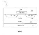
- FIG. 4depicts a cross sectional view of a partially processed integrated circuit up to the completion of a bottom front end of line section
- FIG. 5depicts a cross sectional view of a further processed integrated circuit from FIG. 4 after the formation of a plurality of conductive plugs;
- FIG. 6depicts a cross sectional view of a further processed integrated circuit from FIG. 5 after the partial formation of a middle memory plug section atop the front end of line section;
- FIG. 7depicts a cross sectional view of a further processed integrated circuit from FIG. 6 after the complete formation of a middle memory plug section atop the front end of line section;
- FIG. 8depicts a cross sectional view of a completely processed integrated circuit from FIG. 7 after the complete formation of a top metallization section atop the middle memory plug section;
- FIG. 9depicts a cross sectional view of a completely processed integrated circuit wherein the conductive memory devices of the middle memory plug section further include features of a hard mask layer and a spacer;
- FIG. 10A through FIG. 10Edetail an exemplary sequence of various processing steps that could be used for the creation of the hard mask and spacer features of the conductive memory devices of FIG. 9 ;
- FIG. 11depicts a cross sectional view of a completely processed integrated circuit wherein the conductive memory devices of the middle memory plug section further include an optional undercut feature.
- FIG. 1Adepicts a perspective view of an exemplary cross point memory array 100 employing a single layer of memory.
- a bottom layer of x-direction conductive array lines 105is orthogonal to a top layer of y-direction conductive array lines 110 .
- the x-direction conductive array lines 105act as a first terminal and the y-direction conductive array lines 110 act as a second terminal to a plurality of memory plugs 115 , which are located at the intersections of the conductive array lines 105 and 110 .
- the conductive array lines 105 and 110are used to both deliver a voltage pulse to the memory plugs 115 and carry current through the memory plugs 115 in order to determine their resistive states.
- Conductive array line layers 105 and 110can generally be constructed of any conductive material, such as aluminum, copper, tungsten or certain ceramics. Depending upon the material, a conductive array line would typically cross between 64 and 8192 perpendicular conductive array lines. Fabrication techniques, feature size and resistivity of material may allow for shorter or longer lines. Although the x-direction and y-direction conductive array lines can be of equal lengths (forming a square cross point array) they can also be of unequal lengths (forming a rectangular cross point array).
- FIG. 2Aillustrates selection of a memory cell 205 in the cross point array 100 .
- the point of intersection between a single x-direction conductive array line 210 and a single y-direction conductive array line 215uniquely identifies the single memory cell 205 .
- FIG. 2Billustrates the boundaries of the selected memory cell 205 .
- the memory cellis a repeatable unit that can be theoretically extended in one, two or even three dimensions.
- One method of repeating the memory cells in the z-directionis to use both the bottom and top surfaces of conductive array lines 105 and 110 .
- FIG. 1Bdepicts an exemplary stacked cross point array 150 employing four memory layers 155 , 160 , 165 , and 170 .
- the memory layersare sandwiched between alternating layers of x-direction conductive array lines 175 , 180 and 185 and y-direction conductive array lines 190 and 195 such that each memory layer 155 , 160 , 165 , and 170 is associated with only one x-direction conductive array line layer and one y-direction conductive array line layer.
- top conductive array line layer 185 and bottom conductive array line layer 175are only used to supply voltage to a single memory layer 155 and 170
- the other conductive array line layers 180 , 190 , and 195can be used to supply voltage to both a top and a bottom memory layer 155 , 160 , 165 , or 170 .
- the repeatable cell that makes up the cross point array 100can be considered to be a memory plug 255 , plus 1 ⁇ 2 of the space around the memory plug, plus 1 ⁇ 2 of an x-direction conductive array line 210 and 1 ⁇ 2 of a y-direction conductive array line 215 .
- 1 ⁇ 2 of a conductive array lineis merely a theoretical construct, since a conductive array line would generally be fabricated to the same width, regardless of whether one or both surfaces of the conductive array line was used. Accordingly, the very top and very bottom layers of conductive array lines (which use only one surface) would typically be fabricated to the same size as all other layers of conductive array lines.
- cross point arrayOne benefit of the cross point array is that the active circuitry that drives the cross point array 100 or 150 can be placed beneath the cross point array, therefore reducing the footprint required on a semiconductor substrate.
- the cross point arrayis not the only type of memory array that can be used with a two-terminal memory element.
- a two-dimensional transistor memory arraycan incorporate a two-terminal memory element. While the memory element in such an array would be a two-terminal device, the entire memory cell would be a three-terminal device.
- FIG. 3is a generalized diagrammatic representation of a memory cell 300 that can be used in a transistor memory array.
- Each memory cell 300includes a transistor 305 and a memory plug 310 .
- the transistor 305is used to permit current from the data line 315 to access the memory plug 310 when an appropriate voltage is applied to the select line 320 , which is also the transistor's gate.
- the reference line 325might span two cells if the adjacent cells are laid out as the mirror images of each other.
- Each memory plug 255 or 310contains a multi-resistive state element (described later) along with any other materials that may be desirable for fabrication or functionality.
- the additional materialsmight include a non-ohmic device, as is described in co-pending application “High Density NVRAM,” U.S. application Ser. No. 10/360,005, filed Feb. 7, 2003, incorporated herein by reference in its entirety for all purposes.
- the non-ohmic deviceexhibits a very high resistance regime for a certain range of voltages (V NO ⁇ to V NO+ ) and a very low resistance regime for voltages above and below that range.
- the non-ohmic devicemay cause the memory plug 255 or 310 to exhibit a non-linear resistive characteristic.
- exemplary non-ohmic devicesinclude three-film metal-insulator-metal (MIM) structures and back-to-back diodes in series.
- Electrodeswill typically be desirable components of the memory plugs 255 or 310 , a pair of electrodes sandwiching the multi-resistive state element. If the only purpose of the electrodes is as a barrier to prevent metal inter-diffusion, then a thin layer of metal, e.g. TiN, Pt, Au, Ag and Al. could be used. However, conductive oxide electrodes may provide advantages beyond simply acting as a metal inter-diffusion Co-pending U.S. patent application, “Conductive Memory Device With Barrier Electrodes,” U.S. application Ser. No. 10/682,277, filed Oct.
- Electrodesformed either with a single layer or multiple layers that prevent the diffusion of metals, oxygen, hydrogen and water, act as a seed layer in order to form a good lattice match with the conductive memory element, include adhesion layers, and reduce stress caused by uneven coefficients of thermal expansion, and provide other benefits. Additionally, the choice of electrode layers in combination with the multi-resistive state element layer may affect the properties of the memory plug 255 or 310 , as is described in co-pending U.S. patent application, “Resistive Memory Device With A Treated Interface,” U.S. application Ser. No. 10/665,882, filed Sep. 19, 2003, incorporated herein by reference in its entirety for all purposes.
- the multi-resistive state elementwill generally, but not necessarily, be crystalline, either as a single crystalline structure or a polycrystalline structure.
- One class of multi-resistive state elementare perovskites that include two or more metals, the metals being selected from the group consisting of transition metals, alkaline earth metals and rare earth metals.
- the perovskitescan be any number of compositions, including manganites (e.g., Pr 07 Ca 03 MnO 3 , Pro 0.5 Cao 0.5 MnO 3 and other PCMOs, LCMOs, etc.), titanates (e.g., STO:Cr), zirconates (e.g., SZO:Cr), other materials such as Ca 2 Nb 2 O 7 :Cr, and Ta 2 O 5 :Cr, and high Tc superconductors (e.g., YBCO).
- manganitese.g., Pr 07 Ca 03 MnO 3 , Pro 0.5 Cao 0.5 MnO 3 and other PCMOs, LCMOs, etc.
- titanatese.g., STO:Cr
- zirconatese.g., SZO:Cr
- other materialssuch as Ca 2 Nb 2 O 7 :Cr, and Ta 2 O 5 :Cr
- high Tc superconductorse.g.,
- MnO 3when combined with the rare earth metals La, Pr or some combination thereof and the alkaline earth metals Ca, Sr or some combination thereof have been found to produce a particularly effective multi-resistive state element for use in the memory plug 255 or 310 .
- the compounds that make up the perovskite class of multi-resistive state elementsinclude both simple conductive metal oxides and complex conductive metal oxides. Further, some oxides that may not be conductive in their pure form may be used as they become conductive through the addition of dopants, or if they are used as a very thin layer (e.g., in the order of tens of Angstroms) in which case tunneling conduction can be achieved. Therefore, as will be appreciated by those skilled in the art, the terms “conductive memory” and “conductive device” can include devices that are fabricated with materials that are classified as insulators, but are thin enough to allow tunneling conduction.
- Multi-resistive state elementsare not limited to perovskites. Specifically, any material that has a hysteresis that exhibits a resistive state change upon application of a voltage while allowing non-destructive reads is a good candidate for a multi-resistive state element.
- a non-destructive readmeans that the read operation has no effect on the resistive state of the memory element. Measuring the resistance of a memory cell is accomplished by detecting either current after the memory cell is held to a known voltage, or voltage after a known current flows through the memory cell.
- a multi-resistive state materialthat is placed in a high resistive state R 0 upon application of ⁇ V W and a low resistive state R 1 upon application of +V W should be unaffected by a read operation performed at ⁇ V R or +V R . In such materials a write operation is not necessary after a read operation.
- the same principleapplies if more that one resistive state is used to store information (e.g., the multi-resistive state element has a high resistive state of R 00 , a medium-high resistive state of R 01 , a medium-low resistive state of R 10 and a low resistive state of R 11 ).
- fabrication of the multi-resistive state elementmight include additional techniques in order to ensure an effective memory device. For example, biasing the multi-resistive state element might be required in order to ensure the hysteresis is presented in a certain direction.
- Co-pending U.S. patent application, “Multi-Layer Conductive Memory Device,” U.S. application Ser. No. 10/605,757, filed Oct. 23, 2003, incorporated herein by reference in its entirety for all purposesdescribes using a multi-layered multi-resistive state element in order to encourage a hysteresis in a certain direction.
- the fabrication techniques used for the memory plug 255 or 310will typically dictate the requirements of the layers beneath the memory plug (e.g., in a transistor memory array the select line 320 ; and in a cross point array 100 or 150 the driver circuitry and conductive lines 105 , 175 , 180 , 190 and 195 ). Since certain fabrication processes (e.g., solution based spin on followed by high temperature anneal, pulsed laser deposition, sputtering, and metal-organic chemical vapor deposition) might require high temperatures, refractory metals should be used for these layers so that they may withstand the temperatures. However, refractive metals have higher resistances, which may limit the number of cells on an array. Co-pending U.S.
- FIG. 4depicts a cross sectional view of a partially processed integrated circuit up to the completion of a bottom front end of line (FEOL) processed section 600 .
- a p-type substrate 610lies beneath an n-well 615 that in turn lies underneath a p-well 620 .
- Two N+ lands 625 and 630are created within the p-well 620 to form reverse-biased p-n junctions.
- a first inter-layer dielectric (ILD) 605is formed atop the p-well 620 .
- a select line 635can be formed, within the first ILD 605 , with a standard polysilicon gate controllably turning on a field effect transistor (FET) type of conduction between the two N+ lands 625 and 630 .
- FETfield effect transistor
- the selected FEOL processcan be any of the many standard IC processes such as Silicon, Germanium, Gallium Arsenide, Silicon-Germanium and Silicon on Insulator.
- FEOL processesare generally defined as operations performed on a semiconductor wafer in the course of device manufacturing up to but just before first metallization, and might end with chemical-mechanical polishing (CMP) of the first ILD 605 .
- CMPchemical-mechanical polishing
- FIG. 5depicts a cross sectional view of a further processed integrated circuit 700 after conductive plugs are formed in the FEOL section 600 of FIG. 4 .
- a number of contact holesare first formed through the first ILD 605 .
- Barrier/adhesion layers 705 and 710can then sputtered inside the contact holes.
- sputteringis a form of physical vapor deposition technique. The specific sputtering composition will depend on the conductive plug material being used, and can be 100 ⁇ Ti followed by 200 ⁇ of TiN.
- a conductive plug materialcan be deposited within the contact holes atop the barrier/adhesion layers 705 and 710 .
- the conductive plugcan be Tungsten (W)-plug 715 and Tungsten (W)-plug 720 deposited with 5000 ⁇ of W using chemical vapor deposition (CVD) followed by an etchback process or chemical-mechanical polishing (CMP) to remove excess conductive plug material atop the first ILD 605 surface.
- CVDchemical vapor deposition
- CMPchemical-mechanical polishing
- FIG. 6depicts a cross sectional view of a further processed integrated circuit 800 after the partial formation of a middle memory plug section atop the partially processed integrated circuit 700 from FIG. 5 .
- a bottom electrode 805is deposited.
- the bottom electrode 805can in turn be made of multiple layers, such as a 500 ⁇ thick barrier layer of TiAlN to prevent metal inter-diffusion followed by a 500 ⁇ LaNiO 3 or 1000 ⁇ Pt. These layers can be deposited by sputtering.
- a multi-resistive state element 810is deposited on top of the bottom electrode 805 .
- the multi-resistive state element 810is typically made of a conductive metal oxide and can be 2000 ⁇ of a material having a stoichiometry of Pro 0.7 Ca 0.3 MnO 3 (PCMO) and is preferably deposited at less than or equal to about 600° C. by a physical vapor deposition technique such as sputtering, followed by annealing. The annealing step helps to recover the intended crystalline structure and material composition of the multi-resistive state element 810 . Next, a top electrode 815 that can have a composition similar to the bottom electrode 805 can be deposited using sputtering.
- PCMOPro 0.7 Ca 0.3 MnO 3
- bottom electrode 805 and the top electrode 815can be made of a conductive layer and a barrier layer to prevent metal inter-diffusion. See copending application entitled “Conductive Memory Device With Barrier Electrodes,” filed Oct. 8, 2003, U.S. application Ser. No. 10/682,277, already incorporated herein by reference, for further details.
- the target surface, the supplier of the material to be sputtered, and the substrate surface, the receiver of the material to be sputteredare oriented approximately orthogonal to each other, about 70 to 90 degrees.
- the advantage of the off-axis sputteringincludes minimizing material damage from ion impingement during an on-axis reactive ion sputtering process.
- the deposited materialsare sputtered from more than one target concurrently so as to create a plasma of more than one material, hence the deposition of more than one material on the substrate surface at the same time.
- the advantage of co-sputteringincludes flexibility of material composition.
- in-situ multi-layer film depositiontakes place inside the same deposition chamber without breaking the vacuum.
- This deposition techniqueis most easily accomplished, for example, in a sputtering machine by keeping the substrate at one location while switching targets or by switching deposition chambers within one system. By not breaking the vacuum, numerous contamination and oxidation problems from exposure to air are avoided.
- the deposition of the multi-resistive state element 810can advantageously employ the co-sputtering technique. At least one of the three sputtering processes for the bottom electrode 805 , the multi-resistive state element 810 and the top electrode 815 can employ the off-axis sputtering technique. Furthermore, out of these three sputtering processes, at least two consecutive sputtering processes can advantageously use the continuous deposition technique. As another option, an etch stop/diffusion barrier 820 might then be deposited to protect the PCMO from inter-diffusion. The etch stop/diffusion barrier 820 would surround the exposed surfaces of the bottom electrode 805 , top electrode 815 and multi-resistive state element 810 as shown.
- the etch stop/diffusion barrier 820is a dual-function layer also acting as an etch stop in the fabrication process. Notice also that the etch stop/diffusion barrier 820 forms a sidewall layer that surrounds the side surfaces of the bottom electrode 805 , the multi-resistive state element 810 and the top electrode 815 .
- the etch stop/diffusion barrier 820can be made of 250 ⁇ of Si 3 N 4 , TiO 2 or Al 2 O 3 .
- the deposition of the multi-resistive state element 810can be followed by modification of the interface property between the multi-resistive state element 810 and the later deposited top electrode 815 . More specifically, the modification of the interface property can be done by ion implantation, in situ plasma treatment in various gasses, or in situ annealing in various gasses. Possible gasses might include argon, oxygen or hydrogen.
- FIG. 7depicts a cross sectional view of a further processed integrated circuit 900 after the complete formation of a middle memory plug section atop the partially processed integrated circuit 800 of FIG. 6 .
- the middle memory plug sectionincludes all IC components above the top surface of the first ILD 605 , as shown in FIG. 5 , up to the top surface of a second ILD 905 .
- the second ILD 905is deposited on top of the etch stop/diffusion barrier 820 .
- the second ILD 905can be made of a thick SiO 2 layer and then planarized by chemical-mechanical polishing (CMP).
- CMPchemical-mechanical polishing
- a plurality of via holes, locationally and geometrically corresponding to the top electrode 815can then be formed with standard photolithography and via etch.
- Barrier/adhesion layers 910 and 915are then sputtered inside the via holes.
- the specific sputtering compositioncan be 100 ⁇ Ti followed by 200 ⁇ of TiN.
- a conductive plug materialis deposited within the contact holes atop the barrier/adhesion layers 910 and 915 .
- the conductive plugcan be W-plug 920 and W-plug 925 deposited with 5000 ⁇ of W using chemical vapor deposition (CVD) followed by an etchback process or CMP to remove excess conductive plug material atop the second ILD 905 surface.
- CVDchemical vapor deposition
- CMPCMP
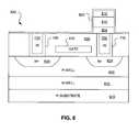
- FIG. 8depicts a cross sectional view of a completely processed integrated circuit 1000 from FIG. 7 after the complete formation of a top metallization section atop the middle memory plug section.
- the top metallization sectionincludes all IC components above the middle memory plug section.
- one or more metallization layerscan be formed above the partially processed integrated circuit 900 of FIG. 7 . Two metallization layers are illustrated in this embodiment. The first metallization layer can be used to form both a reference line 1005 and a metal plug 1010 that eventually connects two W-plugs 920 and 1015 .
- the W-plug 1015is used to connect a data line 1020 , formed during the second metallization layer, to the metal plug 1010 through a third ILD 1025 used to support the data line 1020 .
- the W-plug 1015 and the third ILD 1025are respectively formed with processes similar to those described before. As a process improvement, an annealing step can take place at this point to help recovering the original crystalline structure and material composition of the completed IC.
- any other IC componentscan be implemented instead to connect the bottom electrode 805 to suit a corresponding application.
- Some examplesare a resistor, a capacitor or a non-ohmic device like a diode.
- an X-Y-Z Cartesian coordinate systemcan be set in reference to FIG. 8 : the interfaces between the electrodes 805 and 815 and the multi-resistive state element 810 generally define the X-Y plane while the direction of current through the conductive memory device is essentially parallel to the Z-axis.
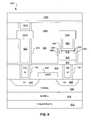
- FIG. 9depicts a cross sectional view of another completely processed integrated circuit 1001 wherein the conductive memory devices of the middle memory plug section further include features of a hard mask 830 layer and a spacer 825 . Except for these features, whose fabrication process is to be presently described, the completely processed integrated circuit 1001 is otherwise the same as the completely processed integrated circuit 1000 depicted in FIG. 8 .
- the spacer 825can be made of a dielectric material surrounding the top electrode 815 . Some examples of the dielectric material are Si 3 N 4 , SiO 2 , TiO 2 , SiON or Al 2 O 3 .
- the hard mask 830is typically made of an electrically conductive material having a similar X-Y cross section as the top electrode 815 .
- the hard mask 830is a masking material that is used as etching mask to protect the film or films underneath from etching in a plasma etch chamber.
- the hard mask materialscan be divided into two categories, insulator or conductor.
- the popular insulating hard mask materialsare oxide and nitride.
- the popular conductive hard mask materialsare binary nitrided metals including TiN, TaN, WN, etc. and ternary nitrided metals including TiSiN, TiAlN, TaSiN, etc.
- One advantage of the hard mask over a standard photo-resistis that the hard mask can resist a dry etching process requiring elevated temperature.
- RIEreactive ion etching
- the introduction of the spacer 825makes the cross sectional area, along the X-Y plane, of the top electrode 815 smaller than that of the multi-resistive state element 810 .
- the spacer 825creates a resistance between the sides of the electrode 815 and the edge of the multi-resistive state element 810 .
- the X-Y footprint of the spacer 825can be made large enough to make the resistance between the sides of the top electrode 815 and the edge of the multi-resistive state element 810 high enough to render the effect of the leakage current conduction negligible.
- FIG. 10A through FIG. 10Edetail an exemplary sequence of various processing steps that could be used for the creation of the hard mask 830 and spacer 825 features of the conductive memory device 1001 of FIG. 9 .
- FIG. 10Aillustrates only a conductive memory device following the steps of sputtering a bottom electrode layer 805 , sputtering a multi-resistive state element layer 810 , sputtering a top electrode layer 815 and depositing a hard mask layer 830 .
- the hard mask layercan be deposited by various means such as Chemical Vapor Deposition, spin coat or sputtering.
- the deposition of the multi-resistive state element 810can be followed by modification of the interface property between the multi-resistive state element 810 and the later deposited top electrode 815 .
- the modification of the interface propertycan be done by ion implantation, in situ argon plasma treatment, in situ oxygen plasma treatment, in situ annealing in argon or in situ annealing in oxygen.
- FIG. 10B and FIG. 10Cillustrate the steps of photo lithographically etching, with a photo resist 835 , the hard mask layer 830 and the top electrode layer 815 both having cross sections smaller than that of a later-patterned multi-resistive state element 810 .
- a dielectric materialis then deposited on top to form the spacer 825 .
- FIG. 10Dillustrates the conductive memory device following an anisotropic dry etching, with a much higher etch rate in the Z-direction than the X-and and Y-directions, of the dielectric material to create a sidewall spacer 825 surrounding the side surfaces of the top electrode 815 and the hard mask 830 .
- FIG. 10Eillustrates the conductive memory device following an etching of the multi-resistive state element layer 810 and the bottom electrode layer 805 .
- an additional clean-up step of wet etchingcan be applied to selectively remove 50-150 ⁇ material of the multi-resistive state element sides, thus forming an undercut.
- FIG. 11depicts a cross sectional view of yet another completely processed integrated circuit 1002 wherein the conductive memory devices of the middle memory plug section include an undercut 840 .
- the X-Y cross section of the bottom electrode 805is larger than that of the multi-resistive state element 810 .
- the X-Y cross section of the top electrode 815is also larger than that of the multi-resistive state element 810 .
- the completely processed integrated circuit 1002is otherwise the same as the completely processed integrated circuit 1000 depicted in FIG. 8 . Referring back to FIG.
- an optional clean-up step of wet etchingcan be applied to selectively remove 50-150 ⁇ of the sides of the multi-resistive state element 810 , thus forming an undercut 840 as shown in FIG. 11 .
- the purpose of the undercut 840is to directly remove the damaged outer periphery of the multi-resistive state element 810 that would otherwise cause an undesirable leakage current conduction in the Z-direction, as explained before.
- each conductive plugmight have a bottom surface area that is larger than the contact hole's top surface area such that each conductive plug has an overhang that is not in contact with the contact hole's top surface area.
- a barrier layer that is in contact with the plug's overhangcould be an advantageous improvement.
- peripheral circuitrysuch as that described in Co-pending U.S. patent application, “An Adaptive Programming Technique for a Re-Writeable Conductive Memory Device,” U.S. application Ser. No.
Landscapes
- Engineering & Computer Science (AREA)
- Chemical & Material Sciences (AREA)
- Materials Engineering (AREA)
- Manufacturing & Machinery (AREA)
- Computer Hardware Design (AREA)
- Semiconductor Memories (AREA)
Abstract
Description
- 1. Field of the Invention
- The present invention relates generally to computer memory, and more specifically to the structure and fabrication of memory elements in an integrated circuit.
- 2. Description of the Related Art
- Memory can either be classified as volatile or nonvolatile. Volatile memory is memory that loses its contents when the power is turned off. In contrast, non-volatile memory does not require a continuous power supply to retain information. Most non-volatile memories use solid-state memory devices as memory elements.
- Certain conductive metal oxides (CMOs), for example, can be used as solid-state memory devices. The CMOs can retain a resistive state after being exposed to an electronic pulse, which can be delivered through two terminals. U.S. Pat. No. 6,204,139, issued Mar. 20, 2001 to Liu et al., incorporated herein by reference for all purposes, describes some perovskite materials that exhibit such characteristics. The perovskite materials are also described by the same researchers in “Electric-pulse-induced reversible resistance change effect in magnetoresistive films,” Applied Physics Letters, Vol. 76, No. 19, 8 May 2000, and “A New Concept for Non-Volatile Memory: The Electric-Pulse Induced Resistive Change Effect in Colossal Magnetoresistive Thin Films,” in materials for the 2001 Non-Volatile Memory Technology Symposium, all of which are hereby incorporated by reference for all purposes. However, the materials described in the U.S. Pat. No. 6,204,139 patent are not generally applicable to RAM memory because the resistance of the material, when scaled to small dimensions, is considered to be too large to make a memory with fast access times.
- In U.S. Pat. No. 6,531,371 entitled “Electrically programmable resistance cross point memory” by Hsu et al, incorporated herein by reference for all purposes, resistive cross point memory devices are disclosed along with methods of manufacture and use. The memory device comprises an active layer of perovskite material interposed between upper electrodes and lower electrodes.
- Similarly, the IBM Zurich Research Center has also published three technical papers that discuss the use of metal oxide material for memory applications: “Reproducible switching effect in thin oxide films for memory applications,” Applied Physics Letters, Vol. 77, No. 1, 3 Jul. 2000, “Current-driven insulator-conductor transition and nonvolatile memory in chromium-doped SrTiO3single crystals,” Applied Physics Letters, Vol. 78, No. 23, 4 Jun. 2001, and “Electric current distribution across a metal-insulator-metal structure during bistable switching,” Journal of Applied Physics, Vol. 90, No. 6, 15 Sep. 2001, all of which are hereby incorporated by reference for all purposes.
- The discovery of the resistance-changing property of certain CMOs, however, is relatively recent and has not yet been implemented in a commercial memory product. There are continuing efforts to bring a true non-volatile RAM (nvRAM) to market.
- In one embodiment the present invention provides a conductive memory device that can be used as a fundamental element in an integrated circuit. Each conductive memory device includes a conductive top and bottom electrode, and a multi-resistive state element. The multi-resistive state element is arranged on top of and in contact with the bottom electrode and the conductive top electrode is arranged on top and in contact with the multi-resistive state element. The conductive memory device is generally operable to be reversibly placed in multiple resistive states.
- A diffusion barrier, typically made of Si3N4, TiO2or Al2O3, and also acting as an etch stop during manufacturing, can be provided to surround the side surfaces of the sandwich of bottom electrode, top electrode and memory material.
- The top electrode cross section can be, to reduce the effect of a leakage current conduction through a damaged outer periphery of the memory material during manufacturing, optionally made smaller than both the bottom electrode and the memory material with the cross sectional difference possibly made up by a dielectric spacer surrounding the side of the top electrode. The spacer can be made of Si3N4, SiO2, TiO2, SiON or Al2O3. To ensure a corresponding manufacturability of the spacer, a hard mask layer can be provided atop the top electrode.
- The memory material cross section can be, to remove a damaged outer periphery of the memory material during manufacturing, optionally made smaller than both the bottom electrode and the top electrode, thus defining an undercut profile.
- To make an integrated circuit including these conductive memory devices, the major steps are typically providing a bottom front end of line (FEOL) section that is a partially processed wafer from a standard IC process, forming a middle memory plug section containing these conductive memory devices and forming a top metallization section.
- To form a plurality of desired conductive plugs, each destined to connect the FEOL circuitry to a bottom electrode of a corresponding conductive memory device, into a first inter-layer dielectric atop the FEOL section the major steps are typically forming a plurality of contact holes through the first inter-layer dielectric, depositing a conductive plug material within the contact holes and removing excess conductive plug material atop the first inter-layer dielectric surface. As an improvement, a barrier/adhesion layer can be formed before depositing the conductive plug material.
- To form the middle memory plug section the major steps are typically sputtering a bottom electrode layer, sputtering a memory material layer, sputtering a top electrode layer and photo lithographically patterning the top electrode, the memory material and the bottom electrode.
- After photo lithographically patterning the top electrode, the memory material and the bottom electrode, an optional wet etching can be applied to remove a damaged outer periphery of the memory material during manufacturing, thus forming the undercut.
- The process of forming the middle memory plug section can include an additional conductive hard mask layer atop the top electrode layer plus an anisotropically etchable dielectric spacer material atop the hard mask layer to form the dielectric spacer.
- As an improvement, one or both of the bottom electrode and the top electrode can be made of a conductive layer and a barrier layer to prevent metal inter-diffusion.
- The formation of the middle memory plug section can further include forming a second inter-layer dielectric atop an intervening etch stop/diffusion barrier.
- The formation of the top metallization section can further include forming, together with a third inter-layer dielectric, one or more metallization layers with standard processes.
- The invention may best be understood by reference to the following description taken in conjunction with the accompanying drawings, in which:
FIG. 1A depicts a perspective view of an exemplary cross point memory array employing a single layer of memory;FIG. 1B depicts a perspective view of an exemplary stacked cross point memory array employing four layer of memory;FIG. 2A depicts a plan view of selection of a memory cell in the cross point array depicted inFIG. 1A ;FIG. 2B depicts a perspective view of the boundaries of the selected memory cell depicted inFIG. 2A ;FIG. 3 depicts a is a generalized representation of a memory cell that can be used in a transistor memory array;FIG. 4 depicts a cross sectional view of a partially processed integrated circuit up to the completion of a bottom front end of line section;FIG. 5 depicts a cross sectional view of a further processed integrated circuit fromFIG. 4 after the formation of a plurality of conductive plugs;FIG. 6 depicts a cross sectional view of a further processed integrated circuit fromFIG. 5 after the partial formation of a middle memory plug section atop the front end of line section;FIG. 7 depicts a cross sectional view of a further processed integrated circuit fromFIG. 6 after the complete formation of a middle memory plug section atop the front end of line section;FIG. 8 depicts a cross sectional view of a completely processed integrated circuit fromFIG. 7 after the complete formation of a top metallization section atop the middle memory plug section;FIG. 9 depicts a cross sectional view of a completely processed integrated circuit wherein the conductive memory devices of the middle memory plug section further include features of a hard mask layer and a spacer;FIG. 10A throughFIG. 10E detail an exemplary sequence of various processing steps that could be used for the creation of the hard mask and spacer features of the conductive memory devices ofFIG. 9 ; andFIG. 11 depicts a cross sectional view of a completely processed integrated circuit wherein the conductive memory devices of the middle memory plug section further include an optional undercut feature.- It is to be understood that, in the drawings, like reference numerals designate like structural elements. Also, it is understood that the depictions in the FIGS are not necessarily to scale.
- In the following description, numerous specific details are set forth to provide a thorough understanding of the present invention. It will be apparent, however, to one skilled in the art that the present invention may be practiced without some or all of these specific details. In other instances, well known process steps have not been described in detail in order to avoid unnecessarily obscuring the present invention.
- The Memory Array
- Conventional nonvolatile memory requires three terminal MOSFET-based devices. The layout of such devices is not ideal, usually requiring an area of at least 8f2for each memory cell, where f is the minimum feature size. However, not all memory elements require three terminals. If, for example, a memory element is capable of changing its electrical properties (e.g., resistivity) in response to a voltage pulse, only two terminals are required. With only two terminals, a cross point array layout that allows a single cell to be fabricated to a size of 4f2can be utilized. Co-pending U.S. patent application, “Cross Point Memory Array Using Multiple Thin Films,” U.S. application Ser. No. 10/330,512, filed Dec. 26, 2002, incorporated herein by reference in its entirety and for all purposes, describes such a device.
FIG. 1A depicts a perspective view of an exemplary crosspoint memory array 100 employing a single layer of memory. A bottom layer of x-directionconductive array lines 105 is orthogonal to a top layer of y-direction conductive array lines110. The x-directionconductive array lines 105 act as a first terminal and the y-directionconductive array lines 110 act as a second terminal to a plurality of memory plugs115, which are located at the intersections of theconductive array lines conductive array lines - Conductive array line layers105 and110 can generally be constructed of any conductive material, such as aluminum, copper, tungsten or certain ceramics. Depending upon the material, a conductive array line would typically cross between 64 and 8192 perpendicular conductive array lines. Fabrication techniques, feature size and resistivity of material may allow for shorter or longer lines. Although the x-direction and y-direction conductive array lines can be of equal lengths (forming a square cross point array) they can also be of unequal lengths (forming a rectangular cross point array).
FIG. 2A illustrates selection of amemory cell 205 in thecross point array 100. The point of intersection between a single x-directionconductive array line 210 and a single y-directionconductive array line 215 uniquely identifies thesingle memory cell 205.FIG. 2B illustrates the boundaries of the selectedmemory cell 205. The memory cell is a repeatable unit that can be theoretically extended in one, two or even three dimensions. One method of repeating the memory cells in the z-direction (orthogonal to the x-y plane) is to use both the bottom and top surfaces ofconductive array lines FIG. 1B depicts an exemplary stackedcross point array 150 employing fourmemory layers conductive array lines conductive array lines memory layer array line layer 185 and bottom conductivearray line layer 175 are only used to supply voltage to asingle memory layer bottom memory layer - Referring back to
FIG. 2B , the repeatable cell that makes up thecross point array 100 can be considered to be amemory plug 255, plus ½ of the space around the memory plug, plus ½ of an x-directionconductive array line 210 and ½ of a y-directionconductive array line 215. Of course, ½ of a conductive array line is merely a theoretical construct, since a conductive array line would generally be fabricated to the same width, regardless of whether one or both surfaces of the conductive array line was used. Accordingly, the very top and very bottom layers of conductive array lines (which use only one surface) would typically be fabricated to the same size as all other layers of conductive array lines. - One benefit of the cross point array is that the active circuitry that drives the
cross point array cross point array 100 and a stackedcross point array 150. - The cross point array is not the only type of memory array that can be used with a two-terminal memory element. For example, a two-dimensional transistor memory array can incorporate a two-terminal memory element. While the memory element in such an array would be a two-terminal device, the entire memory cell would be a three-terminal device.
FIG. 3 is a generalized diagrammatic representation of amemory cell 300 that can be used in a transistor memory array. Eachmemory cell 300 includes atransistor 305 and amemory plug 310. Thetransistor 305 is used to permit current from thedata line 315 to access thememory plug 310 when an appropriate voltage is applied to theselect line 320, which is also the transistor's gate. Thereference line 325 might span two cells if the adjacent cells are laid out as the mirror images of each other. Co-pending U.S. patent application, “Non-Volatile Memory with a Single Transistor and Resistive Memory Element,” U.S. application Ser. No. 10/249,848, filed May 12, 2003, incorporated herein by reference in its entirety for all purposes, describes the specific details of designing and fabricating a transistor memory array.- The Memory Plug
- Each
memory plug memory plug - Furthermore, as described in “Rewriteable Memory With Non-Linear Memory Element,” U.S. application Ser. No. 10/604,556, filed Jul. 30, 2003, incorporated herein by reference in its entirety for all purposes, it may also be possible for the memory cell exhibit non-linear characteristics without a separate non-ohmic device. It should be noted that since it is possible for a memory cell to exhibit non-linear characteristics the terms “resistive memory” and “resistive device” also apply to memories and devices showing non-linear characteristics, and can also be referred to as “conductive memory” and “conductive device.” While a non-ohmic device might be desirable in certain arrays, it may not be helpful in other arrays.
- Electrodes will typically be desirable components of the memory plugs255 or310, a pair of electrodes sandwiching the multi-resistive state element. If the only purpose of the electrodes is as a barrier to prevent metal inter-diffusion, then a thin layer of metal, e.g. TiN, Pt, Au, Ag and Al. could be used. However, conductive oxide electrodes may provide advantages beyond simply acting as a metal inter-diffusion Co-pending U.S. patent application, “Conductive Memory Device With Barrier Electrodes,” U.S. application Ser. No. 10/682,277, filed Oct. 8, 2003, incorporated herein by reference in its entirety for all purposes, describes electrodes (formed either with a single layer or multiple layers) that prevent the diffusion of metals, oxygen, hydrogen and water, act as a seed layer in order to form a good lattice match with the conductive memory element, include adhesion layers, and reduce stress caused by uneven coefficients of thermal expansion, and provide other benefits. Additionally, the choice of electrode layers in combination with the multi-resistive state element layer may affect the properties of the
memory plug memory plug - Multi-resistive state elements, however, are not limited to perovskites. Specifically, any material that has a hysteresis that exhibits a resistive state change upon application of a voltage while allowing non-destructive reads is a good candidate for a multi-resistive state element. A non-destructive read means that the read operation has no effect on the resistive state of the memory element. Measuring the resistance of a memory cell is accomplished by detecting either current after the memory cell is held to a known voltage, or voltage after a known current flows through the memory cell. Therefore, a multi-resistive state material that is placed in a high resistive state R0upon application of −VWand a low resistive state R1upon application of +VWshould be unaffected by a read operation performed at −VRor +VR. In such materials a write operation is not necessary after a read operation. The same principle applies if more that one resistive state is used to store information (e.g., the multi-resistive state element has a high resistive state of R00, a medium-high resistive state of R01, a medium-low resistive state of R10and a low resistive state of R11).
- As described in co-pending U.S. patent application, “A 2-Terminal Trapped Charge Memory device with Voltage Switchable Multi-Level Resistance,” U.S. application Ser. No. 10/634,636, filed Aug. 4, 2003, incorporated herein by reference in its entirety for all purposes, trapped charges are one mechanism by which the hysteresis effect is created. Trapped charges can be encouraged with dopants, as described in co-pending U.S. patent application, “Multi-Resistive State Material that Uses Dopants,” U.S. application Ser. No. 10/604,606, filed Aug. 4, 2003, incorporated herein by reference in its entirety for all purposes.
- It should be appreciated that fabrication of the multi-resistive state element might include additional techniques in order to ensure an effective memory device. For example, biasing the multi-resistive state element might be required in order to ensure the hysteresis is presented in a certain direction. Co-pending U.S. patent application, “Multi-Layer Conductive Memory Device,” U.S. application Ser. No. 10/605,757, filed Oct. 23, 2003, incorporated herein by reference in its entirety for all purposes describes using a multi-layered multi-resistive state element in order to encourage a hysteresis in a certain direction.
- The fabrication techniques used for the
memory plug select line 320; and in across point array conductive lines - Methods of Manufacture
FIG. 4 depicts a cross sectional view of a partially processed integrated circuit up to the completion of a bottom front end of line (FEOL) processedsection 600. A p-type substrate 610 lies beneath an n-well615 that in turn lies underneath a p-well 620. Two N+ lands625 and630 are created within the p-well620 to form reverse-biased p-n junctions. A first inter-layer dielectric (ILD)605 is formed atop the p-well620. Aselect line 635 can be formed, within thefirst ILD 605, with a standard polysilicon gate controllably turning on a field effect transistor (FET) type of conduction between the two N+ lands625 and630. For simplicity and low cost fabrication, the selected FEOL process can be any of the many standard IC processes such as Silicon, Germanium, Gallium Arsenide, Silicon-Germanium and Silicon on Insulator. FEOL processes are generally defined as operations performed on a semiconductor wafer in the course of device manufacturing up to but just before first metallization, and might end with chemical-mechanical polishing (CMP) of thefirst ILD 605. To simplify the description of the present invention, the following embodiments are generally described using a Silicon process with the understanding that the scope of our present invention is not so limited.FIG. 5 depicts a cross sectional view of a further processedintegrated circuit 700 after conductive plugs are formed in theFEOL section 600 ofFIG. 4 . In the process that is shown, a number of contact holes, each corresponding to the location of a desired conductive plug, are first formed through thefirst ILD 605. Barrier/adhesion layers adhesion layers plug 715 and Tungsten (W)-plug 720 deposited with 5000 Å of W using chemical vapor deposition (CVD) followed by an etchback process or chemical-mechanical polishing (CMP) to remove excess conductive plug material atop thefirst ILD 605 surface.FIG. 6 depicts a cross sectional view of a further processedintegrated circuit 800 after the partial formation of a middle memory plug section atop the partially processed integratedcircuit 700 fromFIG. 5 . First, abottom electrode 805 is deposited. Thebottom electrode 805 can in turn be made of multiple layers, such as a 500 Å thick barrier layer of TiAlN to prevent metal inter-diffusion followed by a 500 Å LaNiO3or 1000 Å Pt. These layers can be deposited by sputtering. Next, amulti-resistive state element 810 is deposited on top of thebottom electrode 805. Themulti-resistive state element 810 is typically made of a conductive metal oxide and can be 2000 Å of a material having a stoichiometry of Pro0.7Ca0.3MnO3(PCMO) and is preferably deposited at less than or equal to about 600° C. by a physical vapor deposition technique such as sputtering, followed by annealing. The annealing step helps to recover the intended crystalline structure and material composition of themulti-resistive state element 810. Next, atop electrode 815 that can have a composition similar to thebottom electrode 805 can be deposited using sputtering. Standard photolithography and appropriate multi-step etch processes can then be used to pattern the bottom electrode/multi-resistive state element/top electrode layers into a memory plug. As an optional improvement, one or both of thebottom electrode 805 and thetop electrode 815 can be made of a conductive layer and a barrier layer to prevent metal inter-diffusion. See copending application entitled “Conductive Memory Device With Barrier Electrodes,” filed Oct. 8, 2003, U.S. application Ser. No. 10/682,277, already incorporated herein by reference, for further details.- Numerous sputtering techniques can be employed to further improve the formation of the middle memory plug section. In an off-axis sputtering process, the target surface, the supplier of the material to be sputtered, and the substrate surface, the receiver of the material to be sputtered, are oriented approximately orthogonal to each other, about 70 to 90 degrees. The advantage of the off-axis sputtering includes minimizing material damage from ion impingement during an on-axis reactive ion sputtering process. In a co-sputtering process, the deposited materials are sputtered from more than one target concurrently so as to create a plasma of more than one material, hence the deposition of more than one material on the substrate surface at the same time. Thus, the advantage of co-sputtering includes flexibility of material composition. In a continuous deposition process, in-situ multi-layer film deposition takes place inside the same deposition chamber without breaking the vacuum. This deposition technique is most easily accomplished, for example, in a sputtering machine by keeping the substrate at one location while switching targets or by switching deposition chambers within one system. By not breaking the vacuum, numerous contamination and oxidation problems from exposure to air are avoided.
- Given the above discussion, the deposition of the
multi-resistive state element 810 can advantageously employ the co-sputtering technique. At least one of the three sputtering processes for thebottom electrode 805, themulti-resistive state element 810 and thetop electrode 815 can employ the off-axis sputtering technique. Furthermore, out of these three sputtering processes, at least two consecutive sputtering processes can advantageously use the continuous deposition technique. As another option, an etch stop/diffusion barrier 820 might then be deposited to protect the PCMO from inter-diffusion. The etch stop/diffusion barrier 820 would surround the exposed surfaces of thebottom electrode 805,top electrode 815 andmulti-resistive state element 810 as shown. Notice that the etch stop/diffusion barrier 820 is a dual-function layer also acting as an etch stop in the fabrication process. Notice also that the etch stop/diffusion barrier 820 forms a sidewall layer that surrounds the side surfaces of thebottom electrode 805, themulti-resistive state element 810 and thetop electrode 815. The etch stop/diffusion barrier 820 can be made of 250 Å of Si3N4, TiO2or Al2O3. As a material improvement, the deposition of themulti-resistive state element 810 can be followed by modification of the interface property between themulti-resistive state element 810 and the later depositedtop electrode 815. More specifically, the modification of the interface property can be done by ion implantation, in situ plasma treatment in various gasses, or in situ annealing in various gasses. Possible gasses might include argon, oxygen or hydrogen. FIG. 7 depicts a cross sectional view of a further processedintegrated circuit 900 after the complete formation of a middle memory plug section atop the partially processed integratedcircuit 800 ofFIG. 6 . As a clarification while counting IC components upwards from the bottom, the middle memory plug section includes all IC components above the top surface of thefirst ILD 605, as shown inFIG. 5 , up to the top surface of asecond ILD 905.- The
second ILD 905 is deposited on top of the etch stop/diffusion barrier 820. Thesecond ILD 905 can be made of a thick SiO2layer and then planarized by chemical-mechanical polishing (CMP). A plurality of via holes, locationally and geometrically corresponding to thetop electrode 815, can then be formed with standard photolithography and via etch. Barrier/adhesion layers adhesion layers plug 920 and W-plug 925 deposited with 5000 Å of W using chemical vapor deposition (CVD) followed by an etchback process or CMP to remove excess conductive plug material atop thesecond ILD 905 surface. As a process improvement, an annealing step can take place at this point to help in recovering the original crystalline structure and material composition of the middle memory plug section. FIG. 8 depicts a cross sectional view of a completely processed integratedcircuit 1000 fromFIG. 7 after the complete formation of a top metallization section atop the middle memory plug section. As a clarification while counting IC components upwards from the bottom, the top metallization section includes all IC components above the middle memory plug section. Using standard processes, one or more metallization layers can be formed above the partially processed integratedcircuit 900 ofFIG. 7 . Two metallization layers are illustrated in this embodiment. The first metallization layer can be used to form both areference line 1005 and ametal plug 1010 that eventually connects two W-plugs plug 1015 is used to connect adata line 1020, formed during the second metallization layer, to themetal plug 1010 through athird ILD 1025 used to support thedata line 1020. The W-plug 1015 and thethird ILD 1025 are respectively formed with processes similar to those described before. As a process improvement, an annealing step can take place at this point to help recovering the original crystalline structure and material composition of the completed IC. By now it should become clear to those skilled in the art, while the bottom front end ofline section 600 is shown with the addition of a FET with a terminal ofN+ land 625 connected to thebottom electrode 805 of the conductive memory device via the W-plug 720, in general any other IC components can be implemented instead to connect thebottom electrode 805 to suit a corresponding application. Some examples are a resistor, a capacitor or a non-ohmic device like a diode. To further clarify the spatial orientation and alignment of the conductive memory device an X-Y-Z Cartesian coordinate system can be set in reference toFIG. 8 : the interfaces between theelectrodes multi-resistive state element 810 generally define the X-Y plane while the direction of current through the conductive memory device is essentially parallel to the Z-axis.FIG. 9 depicts a cross sectional view of another completely processed integratedcircuit 1001 wherein the conductive memory devices of the middle memory plug section further include features of ahard mask 830 layer and aspacer 825. Except for these features, whose fabrication process is to be presently described, the completely processed integratedcircuit 1001 is otherwise the same as the completely processed integratedcircuit 1000 depicted inFIG. 8 . Thespacer 825 can be made of a dielectric material surrounding thetop electrode 815. Some examples of the dielectric material are Si3N4, SiO2, TiO2, SiON or Al2O3. Thehard mask 830 is typically made of an electrically conductive material having a similar X-Y cross section as thetop electrode 815. Thehard mask 830 is a masking material that is used as etching mask to protect the film or films underneath from etching in a plasma etch chamber. The hard mask materials can be divided into two categories, insulator or conductor. The popular insulating hard mask materials are oxide and nitride. The popular conductive hard mask materials are binary nitrided metals including TiN, TaN, WN, etc. and ternary nitrided metals including TiSiN, TiAlN, TaSiN, etc. One advantage of the hard mask over a standard photo-resist is that the hard mask can resist a dry etching process requiring elevated temperature. Usually reactive ion etching (RIE) at an elevated temperature is required to etch precious metals or complex metal oxides because of the difficulties associated with their etching, especially the etch byproduct volatility. Due to the impact of previous etch steps defining the profile ofbottom electrode 805,multi-resistive state element 810 andtop electrode 815, the outer periphery of themulti-resistive state element 810 is often damaged by plasma ions, causing a corresponding leakage current conduction in the Z-direction. This leakage current can short out the current conduction through the bulk of themulti-resistive state element 810, and is therefore undesirable and detrimental to the operation of the conductive memory device. The introduction of thespacer 825 makes the cross sectional area, along the X-Y plane, of thetop electrode 815 smaller than that of themulti-resistive state element 810. Thespacer 825 creates a resistance between the sides of theelectrode 815 and the edge of themulti-resistive state element 810. Hence, the X-Y footprint of thespacer 825 can be made large enough to make the resistance between the sides of thetop electrode 815 and the edge of themulti-resistive state element 810 high enough to render the effect of the leakage current conduction negligible.FIG. 10A throughFIG. 10E detail an exemplary sequence of various processing steps that could be used for the creation of thehard mask 830 andspacer 825 features of theconductive memory device 1001 ofFIG. 9 .FIG. 10A illustrates only a conductive memory device following the steps of sputtering abottom electrode layer 805, sputtering a multi-resistivestate element layer 810, sputtering atop electrode layer 815 and depositing ahard mask layer 830. The hard mask layer can be deposited by various means such as Chemical Vapor Deposition, spin coat or sputtering. Like before, the deposition of themulti-resistive state element 810 can be followed by modification of the interface property between themulti-resistive state element 810 and the later depositedtop electrode 815. More specifically, the modification of the interface property can be done by ion implantation, in situ argon plasma treatment, in situ oxygen plasma treatment, in situ annealing in argon or in situ annealing in oxygen.FIG. 10B andFIG. 10C illustrate the steps of photo lithographically etching, with a photo resist835, thehard mask layer 830 and thetop electrode layer 815 both having cross sections smaller than that of a later-patternedmulti-resistive state element 810. A dielectric material is then deposited on top to form thespacer 825.FIG. 10D illustrates the conductive memory device following an anisotropic dry etching, with a much higher etch rate in the Z-direction than the X-and and Y-directions, of the dielectric material to create asidewall spacer 825 surrounding the side surfaces of thetop electrode 815 and thehard mask 830. Finally,FIG. 10E illustrates the conductive memory device following an etching of the multi-resistivestate element layer 810 and thebottom electrode layer 805. As an optional measure to further remove the damaged outer periphery of themulti-resistive state element 810, an additional clean-up step of wet etching can be applied to selectively remove 50-150 Å material of the multi-resistive state element sides, thus forming an undercut.FIG. 11 depicts a cross sectional view of yet another completely processed integratedcircuit 1002 wherein the conductive memory devices of the middle memory plug section include an undercut840. Geometrically, the X-Y cross section of thebottom electrode 805 is larger than that of themulti-resistive state element 810. Similarly, the X-Y cross section of thetop electrode 815 is also larger than that of themulti-resistive state element 810. Except for the undercut840 the completely processed integratedcircuit 1002 is otherwise the same as the completely processed integratedcircuit 1000 depicted inFIG. 8 . Referring back toFIG. 6 and its accompanying description, after patterning the bottom electrode/multi-resistive state element/top electrode layers into a memory plug an optional clean-up step of wet etching can be applied to selectively remove 50-150 Å of the sides of themulti-resistive state element 810, thus forming an undercut840 as shown inFIG. 11 . The purpose of the undercut840 is to directly remove the damaged outer periphery of themulti-resistive state element 810 that would otherwise cause an undesirable leakage current conduction in the Z-direction, as explained before.- Concluding Remarks
- Although the invention has been described in its presently contemplated best mode, it is clear that it is susceptible to numerous modifications, modes of operation and embodiments, all within the ability and skill of those familiar with the art and without exercise of further inventive activity. For example, each conductive plug might have a bottom surface area that is larger than the contact hole's top surface area such that each conductive plug has an overhang that is not in contact with the contact hole's top surface area. In such a case, a barrier layer that is in contact with the plug's overhang could be an advantageous improvement. Additionally, peripheral circuitry, such as that described in Co-pending U.S. patent application, “An Adaptive Programming Technique for a Re-Writeable Conductive Memory Device,” U.S. application Ser. No. 10/680,508, filed Oct. 6, 2003, incorporated herein by reference in its entirety for all purposes, can be easily implemented in the system. Accordingly, that which is intended to be protected by Letters Patent is set forth in the claims and includes all variations and modifications that fall within the spirit and scope of the claim.
Claims (6)
Priority Applications (1)
| Application Number | Priority Date | Filing Date | Title |
|---|---|---|---|
| US11/369,663US7439082B2 (en) | 2003-11-10 | 2006-03-06 | Conductive memory stack with non-uniform width |
Applications Claiming Priority (2)
| Application Number | Priority Date | Filing Date | Title |
|---|---|---|---|
| US10/605,963US7009235B2 (en) | 2003-11-10 | 2003-11-10 | Conductive memory stack with non-uniform width |
| US11/369,663US7439082B2 (en) | 2003-11-10 | 2006-03-06 | Conductive memory stack with non-uniform width |
Related Parent Applications (1)
| Application Number | Title | Priority Date | Filing Date |
|---|---|---|---|
| US10/605,963ContinuationUS7009235B2 (en) | 2002-08-02 | 2003-11-10 | Conductive memory stack with non-uniform width |
Publications (2)
| Publication Number | Publication Date |
|---|---|
| US20060166430A1true US20060166430A1 (en) | 2006-07-27 |
| US7439082B2 US7439082B2 (en) | 2008-10-21 |
Family
ID=34549709
Family Applications (2)
| Application Number | Title | Priority Date | Filing Date |
|---|---|---|---|
| US10/605,963Expired - LifetimeUS7009235B2 (en) | 2002-08-02 | 2003-11-10 | Conductive memory stack with non-uniform width |
| US11/369,663Expired - Fee RelatedUS7439082B2 (en) | 2003-11-10 | 2006-03-06 | Conductive memory stack with non-uniform width |
Family Applications Before (1)
| Application Number | Title | Priority Date | Filing Date |
|---|---|---|---|
| US10/605,963Expired - LifetimeUS7009235B2 (en) | 2002-08-02 | 2003-11-10 | Conductive memory stack with non-uniform width |
Country Status (1)
| Country | Link |
|---|---|
| US (2) | US7009235B2 (en) |
Cited By (5)
| Publication number | Priority date | Publication date | Assignee | Title |
|---|---|---|---|---|
| US20060071262A1 (en)* | 2004-03-01 | 2006-04-06 | Taiwan Semiconductor Manufacturing Co., Ltd. | Metal-insulator-metal (MIM) capacitor structure formed with dual damascene structure |
| US20090072348A1 (en)* | 2007-09-19 | 2009-03-19 | Ulrich Klostermann | Integrated Circuits; Methods for Manufacturing an Integrated Circuit and Memory Module |
| DE102008026711B4 (en)* | 2007-06-04 | 2011-12-01 | Qimonda Ag | A contact integrated circuit comprising semiconductor material sandwiched between sidewalls, and having system integrated circuits and methods of making the same |
| DE102008028802B4 (en)* | 2007-06-21 | 2015-02-05 | Qimonda Ag | Method of manufacturing a memory cell including a vertical diode |
| CN108122903A (en)* | 2016-11-29 | 2018-06-05 | 台湾积体电路制造股份有限公司 | Semiconductor device and layout method |
Families Citing this family (37)
| Publication number | Priority date | Publication date | Assignee | Title |
|---|---|---|---|---|
| US7186569B2 (en)* | 2002-08-02 | 2007-03-06 | Unity Semiconductor Corporation | Conductive memory stack with sidewall |
| US6962648B2 (en)* | 2003-09-15 | 2005-11-08 | Global Silicon Net Corp. | Back-biased face target sputtering |
| US7112815B2 (en)* | 2004-02-25 | 2006-09-26 | Micron Technology, Inc. | Multi-layer memory arrays |
| JP2006060044A (en)* | 2004-08-20 | 2006-03-02 | Canon Anelva Corp | Method for manufacturing magnetoresistive element |
| US7425504B2 (en)* | 2004-10-15 | 2008-09-16 | 4D-S Pty Ltd. | Systems and methods for plasma etching |
| US20060081467A1 (en)* | 2004-10-15 | 2006-04-20 | Makoto Nagashima | Systems and methods for magnetron deposition |
| US20060081466A1 (en)* | 2004-10-15 | 2006-04-20 | Makoto Nagashima | High uniformity 1-D multiple magnet magnetron source |
| US20060273298A1 (en)* | 2005-06-02 | 2006-12-07 | Matrix Semiconductor, Inc. | Rewriteable memory cell comprising a transistor and resistance-switching material in series |
| US7426128B2 (en)* | 2005-07-11 | 2008-09-16 | Sandisk 3D Llc | Switchable resistive memory with opposite polarity write pulses |
| US20070084716A1 (en)* | 2005-10-16 | 2007-04-19 | Makoto Nagashima | Back-biased face target sputtering based high density non-volatile data storage |
| US20070084717A1 (en)* | 2005-10-16 | 2007-04-19 | Makoto Nagashima | Back-biased face target sputtering based high density non-volatile caching data storage |
| US20070205096A1 (en)* | 2006-03-06 | 2007-09-06 | Makoto Nagashima | Magnetron based wafer processing |
| US8395199B2 (en)* | 2006-03-25 | 2013-03-12 | 4D-S Pty Ltd. | Systems and methods for fabricating self-aligned memory cell |
| JP4124243B2 (en)* | 2006-06-05 | 2008-07-23 | セイコーエプソン株式会社 | Storage element manufacturing method, storage element, storage device, electronic device, and transistor manufacturing method |
| US20080011603A1 (en)* | 2006-07-14 | 2008-01-17 | Makoto Nagashima | Ultra high vacuum deposition of PCMO material |
| US8454810B2 (en)* | 2006-07-14 | 2013-06-04 | 4D-S Pty Ltd. | Dual hexagonal shaped plasma source |
| US7932548B2 (en) | 2006-07-14 | 2011-04-26 | 4D-S Pty Ltd. | Systems and methods for fabricating self-aligned memory cell |
| US8308915B2 (en) | 2006-09-14 | 2012-11-13 | 4D-S Pty Ltd. | Systems and methods for magnetron deposition |
| US8208284B2 (en)* | 2008-03-07 | 2012-06-26 | Unity Semiconductor Corporation | Data retention structure for non-volatile memory |
| US8390100B2 (en)* | 2008-12-19 | 2013-03-05 | Unity Semiconductor Corporation | Conductive oxide electrodes |
| KR101083643B1 (en)* | 2008-12-29 | 2011-11-16 | 주식회사 하이닉스반도체 | Resistive memory device and manufacturing method thereof |
| US7969774B2 (en) | 2009-03-10 | 2011-06-28 | Micron Technology, Inc. | Electronic devices formed of two or more substrates bonded together, electronic systems comprising electronic devices and methods of making electronic devices |
| US8487292B2 (en) | 2010-03-16 | 2013-07-16 | Sandisk 3D Llc | Resistance-switching memory cell with heavily doped metal oxide layer |
| US9214628B2 (en) | 2010-12-03 | 2015-12-15 | Panasonic Intellectual Property Management Co., Ltd. | Nonvolatile memory element, nonvolatile memory device, and manufacturing method for the same |
| US9305644B2 (en) | 2011-06-24 | 2016-04-05 | Rambus Inc. | Resistance memory cell |
| JP5636081B2 (en) | 2012-09-26 | 2014-12-03 | パナソニック株式会社 | Nonvolatile memory device and manufacturing method thereof |
| US9331277B2 (en)* | 2013-01-21 | 2016-05-03 | Taiwan Semiconductor Manufacturing Company, Ltd. | One transistor and one resistive random access memory (RRAM) structure with spacer |
| US9048410B2 (en) | 2013-05-31 | 2015-06-02 | Micron Technology, Inc. | Memory devices comprising magnetic tracks individually comprising a plurality of magnetic domains having domain walls and methods of forming a memory device comprising magnetic tracks individually comprising a plurality of magnetic domains having domain walls |
| US9472560B2 (en) | 2014-06-16 | 2016-10-18 | Micron Technology, Inc. | Memory cell and an array of memory cells |
| US9159829B1 (en) | 2014-10-07 | 2015-10-13 | Micron Technology, Inc. | Recessed transistors containing ferroelectric material |
| US9305929B1 (en) | 2015-02-17 | 2016-04-05 | Micron Technology, Inc. | Memory cells |
| KR102392685B1 (en)* | 2015-07-06 | 2022-04-29 | 삼성전자주식회사 | Semiconductor Device Having an Interconnection Structure |
| US10134982B2 (en) | 2015-07-24 | 2018-11-20 | Micron Technology, Inc. | Array of cross point memory cells |
| US9923139B2 (en)* | 2016-03-11 | 2018-03-20 | Micron Technology, Inc. | Conductive hard mask for memory device formation |
| US11170834B2 (en) | 2019-07-10 | 2021-11-09 | Micron Technology, Inc. | Memory cells and methods of forming a capacitor including current leakage paths having different total resistances |
| CN116053308B (en)* | 2023-03-30 | 2023-06-27 | 合肥新晶集成电路有限公司 | Semiconductor structure preparation method and semiconductor structure |
| US20240389486A1 (en)* | 2023-05-15 | 2024-11-21 | Taiwan Semiconductor Manufacturing Company Limited | Capacitor circuit providing self-adjusting capacitance and methods for forming the same |
Citations (28)
| Publication number | Priority date | Publication date | Assignee | Title |
|---|---|---|---|---|
| US3886577A (en)* | 1973-09-12 | 1975-05-27 | Energy Conversion Devices Inc | Filament-type memory semiconductor device and method of making the same |
| US5296716A (en)* | 1991-01-18 | 1994-03-22 | Energy Conversion Devices, Inc. | Electrically erasable, directly overwritable, multibit single cell memory elements and arrays fabricated therefrom |
| US6249014B1 (en)* | 1998-10-01 | 2001-06-19 | Ramtron International Corporation | Hydrogen barrier encapsulation techniques for the control of hydrogen induced degradation of ferroelectric capacitors in conjunction with multilevel metal processing for non-volatile integrated circuit memory devices |
| US20020020836A1 (en)* | 1998-10-19 | 2002-02-21 | Nec Corporation | Thin film capacitor avoiding short circuit between electrodes |
| US6473332B1 (en)* | 2001-04-04 | 2002-10-29 | The University Of Houston System | Electrically variable multi-state resistance computing |
| US6487106B1 (en)* | 1999-01-12 | 2002-11-26 | Arizona Board Of Regents | Programmable microelectronic devices and method of forming and programming same |
| US6531371B2 (en)* | 2001-06-28 | 2003-03-11 | Sharp Laboratories Of America, Inc. | Electrically programmable resistance cross point memory |
| US20030132456A1 (en)* | 1998-09-08 | 2003-07-17 | Yoichi Miyai | Method of forming cross point type DRAM cell |
| US6657888B1 (en)* | 2001-05-11 | 2003-12-02 | Board Of Regents Of The University Of Nebraska | Application of high spin polarization materials in two terminal non-volatile bistable memory devices |
| US6731528B2 (en)* | 2002-05-03 | 2004-05-04 | Micron Technology, Inc. | Dual write cycle programmable conductor memory system and method of operation |
| US6753561B1 (en)* | 2002-08-02 | 2004-06-22 | Unity Semiconductor Corporation | Cross point memory array using multiple thin films |
| US20040141369A1 (en)* | 2003-01-20 | 2004-07-22 | Oki Electric Industry Co., Ltd. | Semiconductor integrated circuit |
| US6807088B2 (en)* | 2003-02-17 | 2004-10-19 | Kabushiki Kaisha Toshiba | Magnetic random access memory and reading method thereof |
| US20040235247A1 (en)* | 2003-05-21 | 2004-11-25 | Sharp Laboratories Of America, Inc. | Asymmetric crystalline structure memory cell |
| US20040233708A1 (en)* | 2003-05-21 | 2004-11-25 | Sharp Laboratories Of America, Inc. | Asymmetric memory cell |
| US6825489B2 (en)* | 2001-04-06 | 2004-11-30 | Axon Technologies Corporation | Microelectronic device, structure, and system, including a memory structure having a variable programmable property and method of forming the same |
| US6836421B2 (en)* | 2002-08-02 | 2004-12-28 | Unity Semiconductor Corporation | Line drivers that fit within a specified line pitch |
| US6856536B2 (en)* | 2002-08-02 | 2005-02-15 | Unity Semiconductor Corporation | Non-volatile memory with a single transistor and resistive memory element |
| US20050070043A1 (en)* | 2003-09-30 | 2005-03-31 | Koji Yamakawa | Semiconductor device and method for manufacturing the same |
| US20050079735A1 (en)* | 2001-11-28 | 2005-04-14 | Seiko Epson Corporation | Substrate for electronic device, method for manufacturing substrate for electronic device, and electronic device |
| US6897532B1 (en)* | 2002-04-15 | 2005-05-24 | Cypress Semiconductor Corp. | Magnetic tunneling junction configuration and a method for making the same |
| US20050135148A1 (en)* | 2003-12-22 | 2005-06-23 | Unity Semiconductor Corporation | Conductive memory array having page mode and burst mode read capability |
| US20050151156A1 (en)* | 2004-01-13 | 2005-07-14 | Wu Naijuan | Switchable resistive perovskite microelectronic device with multi-layer thin film structure |
| US20050167715A1 (en)* | 2002-09-05 | 2005-08-04 | Seiko Epson Corporation | Substrate for electronic devices, manufacturing method therefor, and electronic device |
| US20050201146A1 (en)* | 2003-07-08 | 2005-09-15 | Moore John T. | Method of refreshing a PCRAM memory device |
| US20060023495A1 (en)* | 2002-08-02 | 2006-02-02 | Unity Semiconductor Corporation | High-density NVRAM |
| US7002197B2 (en)* | 2004-01-23 | 2006-02-21 | Hewlett-Packard Development Company, L.P. | Cross point resistive memory array |
| US20070120124A1 (en)* | 2005-11-30 | 2007-05-31 | I-Wei Chen | Resistance-switching oxide thin film devices |
Family Cites Families (5)
| Publication number | Priority date | Publication date | Assignee | Title |
|---|---|---|---|---|
| US6204139B1 (en)* | 1998-08-25 | 2001-03-20 | University Of Houston | Method for switching the properties of perovskite materials used in thin film resistors |
| US6603161B2 (en)* | 2000-03-10 | 2003-08-05 | Kabushiki Kaisha Toshiba | Semiconductor device having ferroelectric capacitor and method for manufacturing the same |
| US6456525B1 (en)* | 2000-09-15 | 2002-09-24 | Hewlett-Packard Company | Short-tolerant resistive cross point array |
| JP2002217381A (en)* | 2000-11-20 | 2002-08-02 | Toshiba Corp | Semiconductor memory device and method of manufacturing the same |
| JP3847645B2 (en)* | 2002-03-20 | 2006-11-22 | 富士通株式会社 | Semiconductor device and manufacturing method thereof |
- 2003
- 2003-11-10USUS10/605,963patent/US7009235B2/ennot_activeExpired - Lifetime
- 2006
- 2006-03-06USUS11/369,663patent/US7439082B2/ennot_activeExpired - Fee Related
Patent Citations (29)
| Publication number | Priority date | Publication date | Assignee | Title |
|---|---|---|---|---|
| US3886577A (en)* | 1973-09-12 | 1975-05-27 | Energy Conversion Devices Inc | Filament-type memory semiconductor device and method of making the same |
| US5296716A (en)* | 1991-01-18 | 1994-03-22 | Energy Conversion Devices, Inc. | Electrically erasable, directly overwritable, multibit single cell memory elements and arrays fabricated therefrom |
| US20030132456A1 (en)* | 1998-09-08 | 2003-07-17 | Yoichi Miyai | Method of forming cross point type DRAM cell |
| US6249014B1 (en)* | 1998-10-01 | 2001-06-19 | Ramtron International Corporation | Hydrogen barrier encapsulation techniques for the control of hydrogen induced degradation of ferroelectric capacitors in conjunction with multilevel metal processing for non-volatile integrated circuit memory devices |
| US20020020836A1 (en)* | 1998-10-19 | 2002-02-21 | Nec Corporation | Thin film capacitor avoiding short circuit between electrodes |
| US6487106B1 (en)* | 1999-01-12 | 2002-11-26 | Arizona Board Of Regents | Programmable microelectronic devices and method of forming and programming same |
| US6473332B1 (en)* | 2001-04-04 | 2002-10-29 | The University Of Houston System | Electrically variable multi-state resistance computing |
| US6825489B2 (en)* | 2001-04-06 | 2004-11-30 | Axon Technologies Corporation | Microelectronic device, structure, and system, including a memory structure having a variable programmable property and method of forming the same |
| US6657888B1 (en)* | 2001-05-11 | 2003-12-02 | Board Of Regents Of The University Of Nebraska | Application of high spin polarization materials in two terminal non-volatile bistable memory devices |
| US6531371B2 (en)* | 2001-06-28 | 2003-03-11 | Sharp Laboratories Of America, Inc. | Electrically programmable resistance cross point memory |
| US20050079735A1 (en)* | 2001-11-28 | 2005-04-14 | Seiko Epson Corporation | Substrate for electronic device, method for manufacturing substrate for electronic device, and electronic device |
| US6897532B1 (en)* | 2002-04-15 | 2005-05-24 | Cypress Semiconductor Corp. | Magnetic tunneling junction configuration and a method for making the same |
| US6731528B2 (en)* | 2002-05-03 | 2004-05-04 | Micron Technology, Inc. | Dual write cycle programmable conductor memory system and method of operation |
| US6753561B1 (en)* | 2002-08-02 | 2004-06-22 | Unity Semiconductor Corporation | Cross point memory array using multiple thin films |
| US20060023495A1 (en)* | 2002-08-02 | 2006-02-02 | Unity Semiconductor Corporation | High-density NVRAM |
| US6836421B2 (en)* | 2002-08-02 | 2004-12-28 | Unity Semiconductor Corporation | Line drivers that fit within a specified line pitch |
| US6856536B2 (en)* | 2002-08-02 | 2005-02-15 | Unity Semiconductor Corporation | Non-volatile memory with a single transistor and resistive memory element |
| US20050167715A1 (en)* | 2002-09-05 | 2005-08-04 | Seiko Epson Corporation | Substrate for electronic devices, manufacturing method therefor, and electronic device |
| US20040141369A1 (en)* | 2003-01-20 | 2004-07-22 | Oki Electric Industry Co., Ltd. | Semiconductor integrated circuit |
| US6807088B2 (en)* | 2003-02-17 | 2004-10-19 | Kabushiki Kaisha Toshiba | Magnetic random access memory and reading method thereof |
| US20040233708A1 (en)* | 2003-05-21 | 2004-11-25 | Sharp Laboratories Of America, Inc. | Asymmetric memory cell |
| US20050207265A1 (en)* | 2003-05-21 | 2005-09-22 | Sharp Laboratories Of America, Inc. | Memory cell with an asymmetric crystalline structure |
| US20040235247A1 (en)* | 2003-05-21 | 2004-11-25 | Sharp Laboratories Of America, Inc. | Asymmetric crystalline structure memory cell |
| US20050201146A1 (en)* | 2003-07-08 | 2005-09-15 | Moore John T. | Method of refreshing a PCRAM memory device |
| US20050070043A1 (en)* | 2003-09-30 | 2005-03-31 | Koji Yamakawa | Semiconductor device and method for manufacturing the same |
| US20050135148A1 (en)* | 2003-12-22 | 2005-06-23 | Unity Semiconductor Corporation | Conductive memory array having page mode and burst mode read capability |
| US20050151156A1 (en)* | 2004-01-13 | 2005-07-14 | Wu Naijuan | Switchable resistive perovskite microelectronic device with multi-layer thin film structure |
| US7002197B2 (en)* | 2004-01-23 | 2006-02-21 | Hewlett-Packard Development Company, L.P. | Cross point resistive memory array |
| US20070120124A1 (en)* | 2005-11-30 | 2007-05-31 | I-Wei Chen | Resistance-switching oxide thin film devices |
Cited By (7)
| Publication number | Priority date | Publication date | Assignee | Title |
|---|---|---|---|---|
| US20060071262A1 (en)* | 2004-03-01 | 2006-04-06 | Taiwan Semiconductor Manufacturing Co., Ltd. | Metal-insulator-metal (MIM) capacitor structure formed with dual damascene structure |
| US7229879B2 (en)* | 2004-03-01 | 2007-06-12 | Taiwan Semiconductor Manufacturing Co., Ltd. | Metal-insulator-metal (MIM) capacitor structure formed with dual damascene structure |
| DE102008026711B4 (en)* | 2007-06-04 | 2011-12-01 | Qimonda Ag | A contact integrated circuit comprising semiconductor material sandwiched between sidewalls, and having system integrated circuits and methods of making the same |
| DE102008028802B4 (en)* | 2007-06-21 | 2015-02-05 | Qimonda Ag | Method of manufacturing a memory cell including a vertical diode |
| US20090072348A1 (en)* | 2007-09-19 | 2009-03-19 | Ulrich Klostermann | Integrated Circuits; Methods for Manufacturing an Integrated Circuit and Memory Module |
| DE102007046956A1 (en)* | 2007-09-19 | 2009-04-02 | Altis Semiconductor Snc | Integrated circuits; Method for manufacturing an integrated circuit and memory module |
| CN108122903A (en)* | 2016-11-29 | 2018-06-05 | 台湾积体电路制造股份有限公司 | Semiconductor device and layout method |
Also Published As
| Publication number | Publication date |
|---|---|
| US7439082B2 (en) | 2008-10-21 |
| US7009235B2 (en) | 2006-03-07 |
| US20050101086A1 (en) | 2005-05-12 |
Similar Documents
| Publication | Publication Date | Title |
|---|---|---|
| US7439082B2 (en) | Conductive memory stack with non-uniform width | |
| US7528405B2 (en) | Conductive memory stack with sidewall | |
| US11502249B2 (en) | Memory element with a reactive metal layer | |
| US7400006B1 (en) | Conductive memory device with conductive oxide electrodes | |
| US7067862B2 (en) | Conductive memory device with conductive oxide electrodes | |
| US7326979B2 (en) | Resistive memory device with a treated interface | |
| US7042035B2 (en) | Memory array with high temperature wiring | |
| US7884349B2 (en) | Selection device for re-writable memory | |
| US6856536B2 (en) | Non-volatile memory with a single transistor and resistive memory element | |
| US7126841B2 (en) | Non-volatile memory with a single transistor and resistive memory element |
Legal Events
| Date | Code | Title | Description |
|---|---|---|---|
| AS | Assignment | Owner name:UNITY SEMICONDUCTOR CORPORATION, CALIFORNIA Free format text:ASSIGNMENT OF ASSIGNORS INTEREST;ASSIGNORS:RINERSON, DARRELL, MR.;CHEVALLIER, CHRISTOPHE, MR.;LONGCOR, STEVEN;REEL/FRAME:020250/0628;SIGNING DATES FROM 20071107 TO 20071108 | |
| AS | Assignment | Owner name:UNITY SEMICONDUCTOR CORPORATION, CALIFORNIA Free format text:CORRECTIVE ASSIGNMENT TO CORRECT THE CHRISTOPHE J. CHEVALLIER TO BE DELETED AS AN INVENTOR. STEVE KUO-REN HSIA TO BE ADDED AS AN INVENTOR AND ASSIGNOR. PREVIOUSLY RECORDED ON REEL 020250 FRAME 0628. ASSIGNOR(S) HEREBY CONFIRMS THE ASSIGNMENT.;ASSIGNORS:RINERSON, DARRELL, MR.;HSIA, STEVE KUO-REN, MR.;LONGCOR, STEVEN W., MR.;REEL/FRAME:021181/0105;SIGNING DATES FROM 20080613 TO 20080617 | |
| STCF | Information on status: patent grant | Free format text:PATENTED CASE | |
| AS | Assignment | Owner name:UNITY SEMICONDUCTOR CORPORATION, CALIFORNIA Free format text:CORRECTIVE ASSIGNMENT TO CORRECT THE ORIGINAL COVERSHEET FOR APPLICATION 11473005 ERRONEOUSLY ATTACHED TO CORRECTIVE ASSIGNMENT FOR APPLICATION 11369663 FILED 7/1/08 PREVIOUSLY RECORDED ON REEL 021181 FRAME 0105;ASSIGNORS:RINERSON, DARRELL, MR.;HSIA, STEVE KUO-REN;LONGCOR, STEVEN W.;REEL/FRAME:021710/0308;SIGNING DATES FROM 20080613 TO 20080617 | |
| CC | Certificate of correction | ||
| AS | Assignment | Owner name:GOLD HILL CAPITAL, CALIFORNIA Free format text:SECURITY AGREEMENT;ASSIGNOR:UNITY SEMICONDUCTOR CORPORATION;REEL/FRAME:023129/0669 Effective date:20090407 Owner name:GOLD HILL CAPITAL,CALIFORNIA Free format text:SECURITY AGREEMENT;ASSIGNOR:UNITY SEMICONDUCTOR CORPORATION;REEL/FRAME:023129/0669 Effective date:20090407 | |
| FEPP | Fee payment procedure | Free format text:PAYOR NUMBER ASSIGNED (ORIGINAL EVENT CODE: ASPN); ENTITY STATUS OF PATENT OWNER: LARGE ENTITY | |
| FEPP | Fee payment procedure | Free format text:PAYER NUMBER DE-ASSIGNED (ORIGINAL EVENT CODE: RMPN); ENTITY STATUS OF PATENT OWNER: LARGE ENTITY Free format text:PAYOR NUMBER ASSIGNED (ORIGINAL EVENT CODE: ASPN); ENTITY STATUS OF PATENT OWNER: LARGE ENTITY Free format text:PAT HOLDER NO LONGER CLAIMS SMALL ENTITY STATUS, ENTITY STATUS SET TO UNDISCOUNTED (ORIGINAL EVENT CODE: STOL); ENTITY STATUS OF PATENT OWNER: LARGE ENTITY | |
| FEPP | Fee payment procedure | Free format text:PAYOR NUMBER ASSIGNED (ORIGINAL EVENT CODE: ASPN); ENTITY STATUS OF PATENT OWNER: LARGE ENTITY Free format text:PAYER NUMBER DE-ASSIGNED (ORIGINAL EVENT CODE: RMPN); ENTITY STATUS OF PATENT OWNER: LARGE ENTITY | |
| FPAY | Fee payment | Year of fee payment:4 | |
| AS | Assignment | Owner name:UNITY SEMICONDUCTOR, INC., CALIFORNIA Free format text:RELEASE;ASSIGNORS:SILICON VALLEY BANK;GOLD HILL CAPITAL;REEL/FRAME:028132/0675 Effective date:20120315 | |
| SULP | Surcharge for late payment | ||
| FPAY | Fee payment | Year of fee payment:8 | |
| FEPP | Fee payment procedure | Free format text:MAINTENANCE FEE REMINDER MAILED (ORIGINAL EVENT CODE: REM.); ENTITY STATUS OF PATENT OWNER: LARGE ENTITY | |
| LAPS | Lapse for failure to pay maintenance fees | Free format text:PATENT EXPIRED FOR FAILURE TO PAY MAINTENANCE FEES (ORIGINAL EVENT CODE: EXP.); ENTITY STATUS OF PATENT OWNER: LARGE ENTITY | |
| STCH | Information on status: patent discontinuation | Free format text:PATENT EXPIRED DUE TO NONPAYMENT OF MAINTENANCE FEES UNDER 37 CFR 1.362 | |
| FP | Lapsed due to failure to pay maintenance fee | Effective date:20201021 |