US20060163683A1 - Luminescent body and optical device including the same - Google Patents
Luminescent body and optical device including the sameDownload PDFInfo
- Publication number
- US20060163683A1 US20060163683A1US10/539,267US53926705AUS2006163683A1US 20060163683 A1US20060163683 A1US 20060163683A1US 53926705 AUS53926705 AUS 53926705AUS 2006163683 A1US2006163683 A1US 2006163683A1
- Authority
- US
- United States
- Prior art keywords
- luminous body
- group
- light
- elements selected
- wavelength converting
- Prior art date
- Legal status (The legal status is an assumption and is not a legal conclusion. Google has not performed a legal analysis and makes no representation as to the accuracy of the status listed.)
- Granted
Links
- 230000003287optical effectEffects0.000titleclaimsdescription28
- 229910052684CeriumInorganic materials0.000claimsabstractdescription31
- 229910052691ErbiumInorganic materials0.000claimsabstractdescription31
- 229910052688GadoliniumInorganic materials0.000claimsabstractdescription31
- 229910052689HolmiumInorganic materials0.000claimsabstractdescription31
- 229910052779NeodymiumInorganic materials0.000claimsabstractdescription31
- 229910052777PraseodymiumInorganic materials0.000claimsabstractdescription31
- 229910052772SamariumInorganic materials0.000claimsabstractdescription31
- 229910052771TerbiumInorganic materials0.000claimsabstractdescription31
- 229910052775ThuliumInorganic materials0.000claimsabstractdescription31
- 229910052769YtterbiumInorganic materials0.000claimsabstractdescription31
- 229910052787antimonyInorganic materials0.000claimsabstractdescription31
- 229910052746lanthanumInorganic materials0.000claimsabstractdescription31
- 229910052718tinInorganic materials0.000claimsabstractdescription31
- 230000002035prolonged effectEffects0.000claimsabstractdescription29
- 229910052692DysprosiumInorganic materials0.000claimsabstractdescription27
- 230000003081coactivatorEffects0.000claimsabstractdescription18
- 239000012190activatorSubstances0.000claimsabstractdescription14
- 230000002708enhancing effectEffects0.000claimsabstractdescription10
- 239000011777magnesiumSubstances0.000claimsdescription40
- 239000000203mixtureSubstances0.000claimsdescription38
- 238000007789sealingMethods0.000claimsdescription33
- 239000011575calciumSubstances0.000claimsdescription31
- 229920005989resinPolymers0.000claimsdescription23
- 239000011347resinSubstances0.000claimsdescription23
- 239000011701zincSubstances0.000claimsdescription23
- 239000011521glassSubstances0.000claimsdescription20
- 239000002019doping agentSubstances0.000claimsdescription19
- 229910052788bariumInorganic materials0.000claimsdescription18
- 229910052791calciumInorganic materials0.000claimsdescription18
- 230000005284excitationEffects0.000claimsdescription18
- 229910052749magnesiumInorganic materials0.000claimsdescription18
- 229910052712strontiumInorganic materials0.000claimsdescription18
- 229910052693EuropiumInorganic materials0.000claimsdescription17
- OGPBJKLSAFTDLK-UHFFFAOYSA-Neuropium atomChemical compound[Eu]OGPBJKLSAFTDLK-UHFFFAOYSA-N0.000claimsdescription17
- 229910052733galliumInorganic materials0.000claimsdescription17
- 239000011572manganeseSubstances0.000claimsdescription17
- 229910052732germaniumInorganic materials0.000claimsdescription13
- 238000002360preparation methodMethods0.000claimsdescription11
- 229910052765LutetiumInorganic materials0.000claimsdescription10
- ATJFFYVFTNAWJD-UHFFFAOYSA-NTinChemical compound[Sn]ATJFFYVFTNAWJD-UHFFFAOYSA-N0.000claimsdescription10
- WATWJIUSRGPENY-UHFFFAOYSA-Nantimony atomChemical compound[Sb]WATWJIUSRGPENY-UHFFFAOYSA-N0.000claimsdescription10
- 229910052797bismuthInorganic materials0.000claimsdescription10
- JCXGWMGPZLAOME-UHFFFAOYSA-Nbismuth atomChemical compound[Bi]JCXGWMGPZLAOME-UHFFFAOYSA-N0.000claimsdescription10
- GWXLDORMOJMVQZ-UHFFFAOYSA-NceriumChemical compound[Ce]GWXLDORMOJMVQZ-UHFFFAOYSA-N0.000claimsdescription10
- KBQHZAAAGSGFKK-UHFFFAOYSA-Ndysprosium atomChemical compound[Dy]KBQHZAAAGSGFKK-UHFFFAOYSA-N0.000claimsdescription10
- UYAHIZSMUZPPFV-UHFFFAOYSA-NerbiumChemical compound[Er]UYAHIZSMUZPPFV-UHFFFAOYSA-N0.000claimsdescription10
- UIWYJDYFSGRHKR-UHFFFAOYSA-Ngadolinium atomChemical compound[Gd]UIWYJDYFSGRHKR-UHFFFAOYSA-N0.000claimsdescription10
- KJZYNXUDTRRSPN-UHFFFAOYSA-Nholmium atomChemical compound[Ho]KJZYNXUDTRRSPN-UHFFFAOYSA-N0.000claimsdescription10
- FZLIPJUXYLNCLC-UHFFFAOYSA-Nlanthanum atomChemical compound[La]FZLIPJUXYLNCLC-UHFFFAOYSA-N0.000claimsdescription10
- OHSVLFRHMCKCQY-UHFFFAOYSA-Nlutetium atomChemical compound[Lu]OHSVLFRHMCKCQY-UHFFFAOYSA-N0.000claimsdescription10
- QEFYFXOXNSNQGX-UHFFFAOYSA-Nneodymium atomChemical compound[Nd]QEFYFXOXNSNQGX-UHFFFAOYSA-N0.000claimsdescription10
- PUDIUYLPXJFUGB-UHFFFAOYSA-Npraseodymium atomChemical compound[Pr]PUDIUYLPXJFUGB-UHFFFAOYSA-N0.000claimsdescription10
- KZUNJOHGWZRPMI-UHFFFAOYSA-Nsamarium atomChemical compound[Sm]KZUNJOHGWZRPMI-UHFFFAOYSA-N0.000claimsdescription10
- GZCRRIHWUXGPOV-UHFFFAOYSA-Nterbium atomChemical compound[Tb]GZCRRIHWUXGPOV-UHFFFAOYSA-N0.000claimsdescription10
- FRNOGLGSGLTDKL-UHFFFAOYSA-Nthulium atomChemical compound[Tm]FRNOGLGSGLTDKL-UHFFFAOYSA-N0.000claimsdescription10
- NAWDYIZEMPQZHO-UHFFFAOYSA-NytterbiumChemical compound[Yb]NAWDYIZEMPQZHO-UHFFFAOYSA-N0.000claimsdescription10
- 229910052748manganeseInorganic materials0.000claimsdescription9
- 239000000460chlorineSubstances0.000claimsdescription8
- 239000011734sodiumSubstances0.000claimsdescription8
- JBQYATWDVHIOAR-UHFFFAOYSA-NtellanylidenegermaniumChemical compound[Te]=[Ge]JBQYATWDVHIOAR-UHFFFAOYSA-N0.000claimsdescription8
- 229910052725zincInorganic materials0.000claimsdescription6
- PWHULOQIROXLJO-UHFFFAOYSA-NManganeseChemical compound[Mn]PWHULOQIROXLJO-UHFFFAOYSA-N0.000claimsdescription5
- 150000004645aluminatesChemical class0.000claimsdescription5
- 150000002500ionsChemical class0.000claimsdescription5
- 239000010409thin filmSubstances0.000claimsdescription5
- WKBOTKDWSSQWDR-UHFFFAOYSA-NBromine atomChemical compound[Br]WKBOTKDWSSQWDR-UHFFFAOYSA-N0.000claimsdescription4
- OYPRJOBELJOOCE-UHFFFAOYSA-NCalciumChemical compound[Ca]OYPRJOBELJOOCE-UHFFFAOYSA-N0.000claimsdescription4
- ZAMOUSCENKQFHK-UHFFFAOYSA-NChlorine atomChemical compound[Cl]ZAMOUSCENKQFHK-UHFFFAOYSA-N0.000claimsdescription4
- PXGOKWXKJXAPGV-UHFFFAOYSA-NFluorineChemical compoundFFPXGOKWXKJXAPGV-UHFFFAOYSA-N0.000claimsdescription4
- DGAQECJNVWCQMB-PUAWFVPOSA-MIlexoside XXIXChemical compoundC[C@@H]1CC[C@@]2(CC[C@@]3(C(=CC[C@H]4[C@]3(CC[C@@H]5[C@@]4(CC[C@@H](C5(C)C)OS(=O)(=O)[O-])C)C)[C@@H]2[C@]1(C)O)C)C(=O)O[C@H]6[C@@H]([C@H]([C@@H]([C@H](O6)CO)O)O)O.[Na+]DGAQECJNVWCQMB-PUAWFVPOSA-M0.000claimsdescription4
- WHXSMMKQMYFTQS-UHFFFAOYSA-NLithiumChemical compound[Li]WHXSMMKQMYFTQS-UHFFFAOYSA-N0.000claimsdescription4
- FYYHWMGAXLPEAU-UHFFFAOYSA-NMagnesiumChemical compound[Mg]FYYHWMGAXLPEAU-UHFFFAOYSA-N0.000claimsdescription4
- ZLMJMSJWJFRBEC-UHFFFAOYSA-NPotassiumChemical compound[K]ZLMJMSJWJFRBEC-UHFFFAOYSA-N0.000claimsdescription4
- 229910052784alkaline earth metalInorganic materials0.000claimsdescription4
- 150000001342alkaline earth metalsChemical class0.000claimsdescription4
- DSAJWYNOEDNPEQ-UHFFFAOYSA-Nbarium atomChemical compound[Ba]DSAJWYNOEDNPEQ-UHFFFAOYSA-N0.000claimsdescription4
- 229910052790berylliumInorganic materials0.000claimsdescription4
- ATBAMAFKBVZNFJ-UHFFFAOYSA-Nberyllium atomChemical compound[Be]ATBAMAFKBVZNFJ-UHFFFAOYSA-N0.000claimsdescription4
- GDTBXPJZTBHREO-UHFFFAOYSA-NbromineSubstancesBrBrGDTBXPJZTBHREO-UHFFFAOYSA-N0.000claimsdescription4
- 229910052794bromiumInorganic materials0.000claimsdescription4
- 229910052793cadmiumInorganic materials0.000claimsdescription4
- BDOSMKKIYDKNTQ-UHFFFAOYSA-Ncadmium atomChemical compound[Cd]BDOSMKKIYDKNTQ-UHFFFAOYSA-N0.000claimsdescription4
- 230000008859changeEffects0.000claimsdescription4
- 229910052801chlorineInorganic materials0.000claimsdescription4
- 229910052731fluorineInorganic materials0.000claimsdescription4
- 239000011737fluorineSubstances0.000claimsdescription4
- 229910052738indiumInorganic materials0.000claimsdescription4
- 229910052744lithiumInorganic materials0.000claimsdescription4
- 229910052758niobiumInorganic materials0.000claimsdescription4
- 229910052700potassiumInorganic materials0.000claimsdescription4
- 239000011591potassiumSubstances0.000claimsdescription4
- 229910052701rubidiumInorganic materials0.000claimsdescription4
- IGLNJRXAVVLDKE-UHFFFAOYSA-Nrubidium atomChemical compound[Rb]IGLNJRXAVVLDKE-UHFFFAOYSA-N0.000claimsdescription4
- 229910052708sodiumInorganic materials0.000claimsdescription4
- CIOAGBVUUVVLOB-UHFFFAOYSA-Nstrontium atomChemical compound[Sr]CIOAGBVUUVVLOB-UHFFFAOYSA-N0.000claimsdescription4
- 229910052715tantalumInorganic materials0.000claimsdescription4
- 229910052720vanadiumInorganic materials0.000claimsdescription4
- 230000005855radiationEffects0.000claimsdescription3
- 239000000758substrateSubstances0.000description21
- 239000002994raw materialSubstances0.000description19
- IJGRMHOSHXDMSA-UHFFFAOYSA-NAtomic nitrogenChemical compoundN#NIJGRMHOSHXDMSA-UHFFFAOYSA-N0.000description18
- AYJRCSIUFZENHW-UHFFFAOYSA-Lbarium carbonateChemical compound[Ba+2].[O-]C([O-])=OAYJRCSIUFZENHW-UHFFFAOYSA-L0.000description18
- VYPSYNLAJGMNEJ-UHFFFAOYSA-NSilicium dioxideChemical compoundO=[Si]=OVYPSYNLAJGMNEJ-UHFFFAOYSA-N0.000description16
- 238000005253claddingMethods0.000description15
- 238000010276constructionMethods0.000description13
- 239000004973liquid crystal related substanceSubstances0.000description11
- XLYOFNOQVPJJNP-UHFFFAOYSA-NwaterSubstancesOXLYOFNOQVPJJNP-UHFFFAOYSA-N0.000description11
- YBMRDBCBODYGJE-UHFFFAOYSA-Ngermanium dioxideChemical compoundO=[Ge]=OYBMRDBCBODYGJE-UHFFFAOYSA-N0.000description10
- UFHFLCQGNIYNRP-UHFFFAOYSA-NHydrogenChemical compound[H][H]UFHFLCQGNIYNRP-UHFFFAOYSA-N0.000description9
- 239000012298atmosphereSubstances0.000description9
- 238000006243chemical reactionMethods0.000description9
- 150000001875compoundsChemical class0.000description9
- RSEIMSPAXMNYFJ-UHFFFAOYSA-Neuropium(III) oxideInorganic materialsO=[Eu]O[Eu]=ORSEIMSPAXMNYFJ-UHFFFAOYSA-N0.000description9
- 239000001257hydrogenSubstances0.000description9
- 229910052739hydrogenInorganic materials0.000description9
- 239000000463materialSubstances0.000description9
- 229910052757nitrogenInorganic materials0.000description9
- 239000004065semiconductorSubstances0.000description9
- XLOMVQKBTHCTTD-UHFFFAOYSA-NZinc monoxideChemical compound[Zn]=OXLOMVQKBTHCTTD-UHFFFAOYSA-N0.000description8
- 239000000919ceramicSubstances0.000description8
- 229910052681coesiteInorganic materials0.000description8
- 229910052593corundumInorganic materials0.000description8
- 229910052906cristobaliteInorganic materials0.000description8
- 238000010586diagramMethods0.000description8
- NLQFUUYNQFMIJW-UHFFFAOYSA-Ndysprosium(III) oxideInorganic materialsO=[Dy]O[Dy]=ONLQFUUYNQFMIJW-UHFFFAOYSA-N0.000description8
- 239000010931goldSubstances0.000description8
- 238000000034methodMethods0.000description8
- 230000008569processEffects0.000description8
- 239000000377silicon dioxideSubstances0.000description8
- 229910052682stishoviteInorganic materials0.000description8
- 229910000018strontium carbonateInorganic materials0.000description8
- LEDMRZGFZIAGGB-UHFFFAOYSA-Lstrontium carbonateChemical compound[Sr+2].[O-]C([O-])=OLEDMRZGFZIAGGB-UHFFFAOYSA-L0.000description8
- 229910019655synthetic inorganic crystalline materialInorganic materials0.000description8
- 229910052905tridymiteInorganic materials0.000description8
- RYGMFSIKBFXOCR-UHFFFAOYSA-NCopperChemical compound[Cu]RYGMFSIKBFXOCR-UHFFFAOYSA-N0.000description7
- 239000012467final productSubstances0.000description7
- 238000010304firingMethods0.000description7
- 238000010438heat treatmentMethods0.000description7
- 230000002730additional effectEffects0.000description6
- 230000002349favourable effectEffects0.000description6
- 229910052594sapphireInorganic materials0.000description6
- 239000010980sapphireSubstances0.000description6
- PNEYBMLMFCGWSK-UHFFFAOYSA-Naluminium oxideInorganic materials[O-2].[O-2].[O-2].[Al+3].[Al+3]PNEYBMLMFCGWSK-UHFFFAOYSA-N0.000description5
- 239000011889copper foilSubstances0.000description5
- 238000009826distributionMethods0.000description5
- 238000001228spectrumMethods0.000description5
- 229910001845yogo sapphireInorganic materials0.000description5
- VTYYLEPIZMXCLO-UHFFFAOYSA-LCalcium carbonateChemical compound[Ca+2].[O-]C([O-])=OVTYYLEPIZMXCLO-UHFFFAOYSA-L0.000description4
- JMASRVWKEDWRBT-UHFFFAOYSA-NGallium nitrideChemical compound[Ga]#NJMASRVWKEDWRBT-UHFFFAOYSA-N0.000description4
- OAICVXFJPJFONN-UHFFFAOYSA-NPhosphorusChemical compound[P]OAICVXFJPJFONN-UHFFFAOYSA-N0.000description4
- 230000000694effectsEffects0.000description4
- QZQVBEXLDFYHSR-UHFFFAOYSA-Ngallium(III) oxideInorganic materialsO=[Ga]O[Ga]=OQZQVBEXLDFYHSR-UHFFFAOYSA-N0.000description4
- CPLXHLVBOLITMK-UHFFFAOYSA-Nmagnesium oxideInorganic materials[Mg]=OCPLXHLVBOLITMK-UHFFFAOYSA-N0.000description4
- 239000000047productSubstances0.000description4
- 238000009877renderingMethods0.000description4
- 238000010521absorption reactionMethods0.000description3
- 239000000853adhesiveSubstances0.000description3
- 230000001070adhesive effectEffects0.000description3
- 230000008901benefitEffects0.000description3
- 239000003795chemical substances by applicationSubstances0.000description3
- 239000010431corundumSubstances0.000description3
- 239000000975dyeSubstances0.000description3
- 239000003822epoxy resinSubstances0.000description3
- 230000005281excited stateEffects0.000description3
- 230000006872improvementEffects0.000description3
- 239000000395magnesium oxideSubstances0.000description3
- 238000002844meltingMethods0.000description3
- 230000008018meltingEffects0.000description3
- 229920000647polyepoxidePolymers0.000description3
- 229920002050silicone resinPolymers0.000description3
- KLZUFWVZNOTSEM-UHFFFAOYSA-KAluminium flourideChemical compoundF[Al](F)FKLZUFWVZNOTSEM-UHFFFAOYSA-K0.000description2
- NLXLAEXVIDQMFP-UHFFFAOYSA-NAmmonia chlorideChemical compound[NH4+].[Cl-]NLXLAEXVIDQMFP-UHFFFAOYSA-N0.000description2
- 230000004888barrier functionEffects0.000description2
- 230000005540biological transmissionEffects0.000description2
- 230000015572biosynthetic processEffects0.000description2
- KGBXLFKZBHKPEV-UHFFFAOYSA-Nboric acidChemical compoundOB(O)OKGBXLFKZBHKPEV-UHFFFAOYSA-N0.000description2
- 239000004327boric acidSubstances0.000description2
- 229910000019calcium carbonateInorganic materials0.000description2
- 229910052802copperInorganic materials0.000description2
- 239000010949copperSubstances0.000description2
- 230000005611electricityEffects0.000description2
- 238000000295emission spectrumMethods0.000description2
- 238000005530etchingMethods0.000description2
- 230000006870functionEffects0.000description2
- 230000036541healthEffects0.000description2
- 238000007731hot pressingMethods0.000description2
- 238000005286illuminationMethods0.000description2
- 230000001965increasing effectEffects0.000description2
- 238000005304joiningMethods0.000description2
- 230000031700light absorptionEffects0.000description2
- 238000004519manufacturing processMethods0.000description2
- 238000002156mixingMethods0.000description2
- 238000000465mouldingMethods0.000description2
- BWHMMNNQKKPAPP-UHFFFAOYSA-Lpotassium carbonateChemical compound[K+].[K+].[O-]C([O-])=OBWHMMNNQKKPAPP-UHFFFAOYSA-L0.000description2
- 230000006798recombinationEffects0.000description2
- 230000009467reductionEffects0.000description2
- 241000894007speciesSpecies0.000description2
- 230000003068static effectEffects0.000description2
- 238000001429visible spectrumMethods0.000description2
- 239000004925Acrylic resinSubstances0.000description1
- 229920000178Acrylic resinPolymers0.000description1
- 229910002704AlGaNInorganic materials0.000description1
- QCDFBFJGMNKBDO-UHFFFAOYSA-NClioquinolChemical compoundC1=CN=C2C(O)=C(I)C=C(Cl)C2=C1QCDFBFJGMNKBDO-UHFFFAOYSA-N0.000description1
- 229910000881Cu alloyInorganic materials0.000description1
- GYHNNYVSQQEPJS-UHFFFAOYSA-NGalliumChemical compound[Ga]GYHNNYVSQQEPJS-UHFFFAOYSA-N0.000description1
- BPQQTUXANYXVAA-UHFFFAOYSA-NOrthosilicateChemical compound[O-][Si]([O-])([O-])[O-]BPQQTUXANYXVAA-UHFFFAOYSA-N0.000description1
- 229910002637Pr6O11Inorganic materials0.000description1
- 230000004913activationEffects0.000description1
- JNDMLEXHDPKVFC-UHFFFAOYSA-Naluminum;oxygen(2-);yttrium(3+)Chemical compound[O-2].[O-2].[O-2].[Al+3].[Y+3]JNDMLEXHDPKVFC-UHFFFAOYSA-N0.000description1
- 235000019270ammonium chlorideNutrition0.000description1
- 239000011230binding agentSubstances0.000description1
- 230000008033biological extinctionEffects0.000description1
- 230000033228biological regulationEffects0.000description1
- 238000005266castingMethods0.000description1
- 230000001413cellular effectEffects0.000description1
- 239000004020conductorSubstances0.000description1
- 239000000470constituentSubstances0.000description1
- 239000013078crystalSubstances0.000description1
- 238000005520cutting processMethods0.000description1
- 230000007423decreaseEffects0.000description1
- 230000003247decreasing effectEffects0.000description1
- DXNVUKXMTZHOTP-UHFFFAOYSA-Ndialuminum;dimagnesium;barium(2+);oxygen(2-)Chemical compound[O-2].[O-2].[O-2].[O-2].[O-2].[O-2].[O-2].[Mg+2].[Mg+2].[Al+3].[Al+3].[Ba+2].[Ba+2]DXNVUKXMTZHOTP-UHFFFAOYSA-N0.000description1
- 238000005516engineering processMethods0.000description1
- 230000007613environmental effectEffects0.000description1
- 239000010408filmSubstances0.000description1
- GNPVGFCGXDBREM-UHFFFAOYSA-Ngermanium atomChemical compound[Ge]GNPVGFCGXDBREM-UHFFFAOYSA-N0.000description1
- PCHJSUWPFVWCPO-UHFFFAOYSA-NgoldChemical compound[Au]PCHJSUWPFVWCPO-UHFFFAOYSA-N0.000description1
- 229910052737goldInorganic materials0.000description1
- 239000008240homogeneous mixtureSubstances0.000description1
- 238000010348incorporationMethods0.000description1
- 229910010272inorganic materialInorganic materials0.000description1
- 239000011147inorganic materialSubstances0.000description1
- 229910052909inorganic silicateInorganic materials0.000description1
- 230000010354integrationEffects0.000description1
- 239000011656manganese carbonateSubstances0.000description1
- 229910000016manganese(II) carbonateInorganic materials0.000description1
- 238000005259measurementMethods0.000description1
- 230000005693optoelectronicsEffects0.000description1
- 229910000027potassium carbonateInorganic materials0.000description1
- 238000003825pressingMethods0.000description1
- 238000005215recombinationMethods0.000description1
- 238000007650screen-printingMethods0.000description1
- 238000000926separation methodMethods0.000description1
- 239000007787solidSubstances0.000description1
- 230000000638stimulationEffects0.000description1
- 238000002211ultraviolet spectrumMethods0.000description1
- 229910019901yttrium aluminum garnetInorganic materials0.000description1
Images


Classifications
- C—CHEMISTRY; METALLURGY
- C09—DYES; PAINTS; POLISHES; NATURAL RESINS; ADHESIVES; COMPOSITIONS NOT OTHERWISE PROVIDED FOR; APPLICATIONS OF MATERIALS NOT OTHERWISE PROVIDED FOR
- C09K—MATERIALS FOR MISCELLANEOUS APPLICATIONS, NOT PROVIDED FOR ELSEWHERE
- C09K11/00—Luminescent, e.g. electroluminescent, chemiluminescent materials
- C09K11/08—Luminescent, e.g. electroluminescent, chemiluminescent materials containing inorganic luminescent materials
- C09K11/77—Luminescent, e.g. electroluminescent, chemiluminescent materials containing inorganic luminescent materials containing rare earth metals
- C09K11/7783—Luminescent, e.g. electroluminescent, chemiluminescent materials containing inorganic luminescent materials containing rare earth metals containing two or more rare earth metals one of which being europium
- C09K11/77924—Aluminosilicates
- C—CHEMISTRY; METALLURGY
- C09—DYES; PAINTS; POLISHES; NATURAL RESINS; ADHESIVES; COMPOSITIONS NOT OTHERWISE PROVIDED FOR; APPLICATIONS OF MATERIALS NOT OTHERWISE PROVIDED FOR
- C09K—MATERIALS FOR MISCELLANEOUS APPLICATIONS, NOT PROVIDED FOR ELSEWHERE
- C09K11/00—Luminescent, e.g. electroluminescent, chemiluminescent materials
- C09K11/08—Luminescent, e.g. electroluminescent, chemiluminescent materials containing inorganic luminescent materials
- C09K11/62—Luminescent, e.g. electroluminescent, chemiluminescent materials containing inorganic luminescent materials containing gallium, indium or thallium
- C—CHEMISTRY; METALLURGY
- C09—DYES; PAINTS; POLISHES; NATURAL RESINS; ADHESIVES; COMPOSITIONS NOT OTHERWISE PROVIDED FOR; APPLICATIONS OF MATERIALS NOT OTHERWISE PROVIDED FOR
- C09K—MATERIALS FOR MISCELLANEOUS APPLICATIONS, NOT PROVIDED FOR ELSEWHERE
- C09K11/00—Luminescent, e.g. electroluminescent, chemiluminescent materials
- C09K11/08—Luminescent, e.g. electroluminescent, chemiluminescent materials containing inorganic luminescent materials
- C09K11/64—Luminescent, e.g. electroluminescent, chemiluminescent materials containing inorganic luminescent materials containing aluminium
- C—CHEMISTRY; METALLURGY
- C09—DYES; PAINTS; POLISHES; NATURAL RESINS; ADHESIVES; COMPOSITIONS NOT OTHERWISE PROVIDED FOR; APPLICATIONS OF MATERIALS NOT OTHERWISE PROVIDED FOR
- C09K—MATERIALS FOR MISCELLANEOUS APPLICATIONS, NOT PROVIDED FOR ELSEWHERE
- C09K11/00—Luminescent, e.g. electroluminescent, chemiluminescent materials
- C09K11/08—Luminescent, e.g. electroluminescent, chemiluminescent materials containing inorganic luminescent materials
- C09K11/66—Luminescent, e.g. electroluminescent, chemiluminescent materials containing inorganic luminescent materials containing germanium, tin or lead
- C—CHEMISTRY; METALLURGY
- C09—DYES; PAINTS; POLISHES; NATURAL RESINS; ADHESIVES; COMPOSITIONS NOT OTHERWISE PROVIDED FOR; APPLICATIONS OF MATERIALS NOT OTHERWISE PROVIDED FOR
- C09K—MATERIALS FOR MISCELLANEOUS APPLICATIONS, NOT PROVIDED FOR ELSEWHERE
- C09K11/00—Luminescent, e.g. electroluminescent, chemiluminescent materials
- C09K11/08—Luminescent, e.g. electroluminescent, chemiluminescent materials containing inorganic luminescent materials
- C09K11/77—Luminescent, e.g. electroluminescent, chemiluminescent materials containing inorganic luminescent materials containing rare earth metals
- C09K11/7783—Luminescent, e.g. electroluminescent, chemiluminescent materials containing inorganic luminescent materials containing rare earth metals containing two or more rare earth metals one of which being europium
- C09K11/7792—Aluminates
- C—CHEMISTRY; METALLURGY
- C09—DYES; PAINTS; POLISHES; NATURAL RESINS; ADHESIVES; COMPOSITIONS NOT OTHERWISE PROVIDED FOR; APPLICATIONS OF MATERIALS NOT OTHERWISE PROVIDED FOR
- C09K—MATERIALS FOR MISCELLANEOUS APPLICATIONS, NOT PROVIDED FOR ELSEWHERE
- C09K11/00—Luminescent, e.g. electroluminescent, chemiluminescent materials
- C09K11/08—Luminescent, e.g. electroluminescent, chemiluminescent materials containing inorganic luminescent materials
- C09K11/77—Luminescent, e.g. electroluminescent, chemiluminescent materials containing inorganic luminescent materials containing rare earth metals
- C09K11/7783—Luminescent, e.g. electroluminescent, chemiluminescent materials containing inorganic luminescent materials containing rare earth metals containing two or more rare earth metals one of which being europium
- C09K11/7793—Germanates
- H—ELECTRICITY
- H01—ELECTRIC ELEMENTS
- H01L—SEMICONDUCTOR DEVICES NOT COVERED BY CLASS H10
- H01L2224/00—Indexing scheme for arrangements for connecting or disconnecting semiconductor or solid-state bodies and methods related thereto as covered by H01L24/00
- H01L2224/01—Means for bonding being attached to, or being formed on, the surface to be connected, e.g. chip-to-package, die-attach, "first-level" interconnects; Manufacturing methods related thereto
- H01L2224/02—Bonding areas; Manufacturing methods related thereto
- H01L2224/04—Structure, shape, material or disposition of the bonding areas prior to the connecting process
- H01L2224/05—Structure, shape, material or disposition of the bonding areas prior to the connecting process of an individual bonding area
- H01L2224/05001—Internal layers
- H01L2224/0502—Disposition
- H01L2224/05023—Disposition the whole internal layer protruding from the surface
- H—ELECTRICITY
- H01—ELECTRIC ELEMENTS
- H01L—SEMICONDUCTOR DEVICES NOT COVERED BY CLASS H10
- H01L2224/00—Indexing scheme for arrangements for connecting or disconnecting semiconductor or solid-state bodies and methods related thereto as covered by H01L24/00
- H01L2224/01—Means for bonding being attached to, or being formed on, the surface to be connected, e.g. chip-to-package, die-attach, "first-level" interconnects; Manufacturing methods related thereto
- H01L2224/02—Bonding areas; Manufacturing methods related thereto
- H01L2224/04—Structure, shape, material or disposition of the bonding areas prior to the connecting process
- H01L2224/05—Structure, shape, material or disposition of the bonding areas prior to the connecting process of an individual bonding area
- H01L2224/05001—Internal layers
- H01L2224/05075—Plural internal layers
- H01L2224/0508—Plural internal layers being stacked
- H—ELECTRICITY
- H01—ELECTRIC ELEMENTS
- H01L—SEMICONDUCTOR DEVICES NOT COVERED BY CLASS H10
- H01L2224/00—Indexing scheme for arrangements for connecting or disconnecting semiconductor or solid-state bodies and methods related thereto as covered by H01L24/00
- H01L2224/01—Means for bonding being attached to, or being formed on, the surface to be connected, e.g. chip-to-package, die-attach, "first-level" interconnects; Manufacturing methods related thereto
- H01L2224/02—Bonding areas; Manufacturing methods related thereto
- H01L2224/04—Structure, shape, material or disposition of the bonding areas prior to the connecting process
- H01L2224/05—Structure, shape, material or disposition of the bonding areas prior to the connecting process of an individual bonding area
- H01L2224/0554—External layer
- H01L2224/0556—Disposition
- H01L2224/05568—Disposition the whole external layer protruding from the surface
- H—ELECTRICITY
- H01—ELECTRIC ELEMENTS
- H01L—SEMICONDUCTOR DEVICES NOT COVERED BY CLASS H10
- H01L2224/00—Indexing scheme for arrangements for connecting or disconnecting semiconductor or solid-state bodies and methods related thereto as covered by H01L24/00
- H01L2224/01—Means for bonding being attached to, or being formed on, the surface to be connected, e.g. chip-to-package, die-attach, "first-level" interconnects; Manufacturing methods related thereto
- H01L2224/02—Bonding areas; Manufacturing methods related thereto
- H01L2224/04—Structure, shape, material or disposition of the bonding areas prior to the connecting process
- H01L2224/06—Structure, shape, material or disposition of the bonding areas prior to the connecting process of a plurality of bonding areas
- H01L2224/061—Disposition
- H01L2224/06102—Disposition the bonding areas being at different heights
- H—ELECTRICITY
- H01—ELECTRIC ELEMENTS
- H01L—SEMICONDUCTOR DEVICES NOT COVERED BY CLASS H10
- H01L2224/00—Indexing scheme for arrangements for connecting or disconnecting semiconductor or solid-state bodies and methods related thereto as covered by H01L24/00
- H01L2224/01—Means for bonding being attached to, or being formed on, the surface to be connected, e.g. chip-to-package, die-attach, "first-level" interconnects; Manufacturing methods related thereto
- H01L2224/10—Bump connectors; Manufacturing methods related thereto
- H01L2224/15—Structure, shape, material or disposition of the bump connectors after the connecting process
- H01L2224/16—Structure, shape, material or disposition of the bump connectors after the connecting process of an individual bump connector
- H01L2224/161—Disposition
- H01L2224/16135—Disposition the bump connector connecting between different semiconductor or solid-state bodies, i.e. chip-to-chip
- H01L2224/16145—Disposition the bump connector connecting between different semiconductor or solid-state bodies, i.e. chip-to-chip the bodies being stacked
- H—ELECTRICITY
- H01—ELECTRIC ELEMENTS
- H01L—SEMICONDUCTOR DEVICES NOT COVERED BY CLASS H10
- H01L2224/00—Indexing scheme for arrangements for connecting or disconnecting semiconductor or solid-state bodies and methods related thereto as covered by H01L24/00
- H01L2224/01—Means for bonding being attached to, or being formed on, the surface to be connected, e.g. chip-to-package, die-attach, "first-level" interconnects; Manufacturing methods related thereto
- H01L2224/10—Bump connectors; Manufacturing methods related thereto
- H01L2224/15—Structure, shape, material or disposition of the bump connectors after the connecting process
- H01L2224/17—Structure, shape, material or disposition of the bump connectors after the connecting process of a plurality of bump connectors
- H01L2224/1701—Structure
- H01L2224/1703—Bump connectors having different sizes, e.g. different diameters, heights or widths
- H—ELECTRICITY
- H01—ELECTRIC ELEMENTS
- H01L—SEMICONDUCTOR DEVICES NOT COVERED BY CLASS H10
- H01L2224/00—Indexing scheme for arrangements for connecting or disconnecting semiconductor or solid-state bodies and methods related thereto as covered by H01L24/00
- H01L2224/01—Means for bonding being attached to, or being formed on, the surface to be connected, e.g. chip-to-package, die-attach, "first-level" interconnects; Manufacturing methods related thereto
- H01L2224/42—Wire connectors; Manufacturing methods related thereto
- H01L2224/47—Structure, shape, material or disposition of the wire connectors after the connecting process
- H01L2224/48—Structure, shape, material or disposition of the wire connectors after the connecting process of an individual wire connector
- H01L2224/4805—Shape
- H01L2224/4809—Loop shape
- H01L2224/48091—Arched
- H—ELECTRICITY
- H01—ELECTRIC ELEMENTS
- H01L—SEMICONDUCTOR DEVICES NOT COVERED BY CLASS H10
- H01L2224/00—Indexing scheme for arrangements for connecting or disconnecting semiconductor or solid-state bodies and methods related thereto as covered by H01L24/00
- H01L2224/01—Means for bonding being attached to, or being formed on, the surface to be connected, e.g. chip-to-package, die-attach, "first-level" interconnects; Manufacturing methods related thereto
- H01L2224/42—Wire connectors; Manufacturing methods related thereto
- H01L2224/47—Structure, shape, material or disposition of the wire connectors after the connecting process
- H01L2224/48—Structure, shape, material or disposition of the wire connectors after the connecting process of an individual wire connector
- H01L2224/481—Disposition
- H01L2224/48151—Connecting between a semiconductor or solid-state body and an item not being a semiconductor or solid-state body, e.g. chip-to-substrate, chip-to-passive
- H01L2224/48221—Connecting between a semiconductor or solid-state body and an item not being a semiconductor or solid-state body, e.g. chip-to-substrate, chip-to-passive the body and the item being stacked
- H01L2224/48245—Connecting between a semiconductor or solid-state body and an item not being a semiconductor or solid-state body, e.g. chip-to-substrate, chip-to-passive the body and the item being stacked the item being metallic
- H01L2224/48247—Connecting between a semiconductor or solid-state body and an item not being a semiconductor or solid-state body, e.g. chip-to-substrate, chip-to-passive the body and the item being stacked the item being metallic connecting the wire to a bond pad of the item
- H—ELECTRICITY
- H01—ELECTRIC ELEMENTS
- H01L—SEMICONDUCTOR DEVICES NOT COVERED BY CLASS H10
- H01L2224/00—Indexing scheme for arrangements for connecting or disconnecting semiconductor or solid-state bodies and methods related thereto as covered by H01L24/00
- H01L2224/01—Means for bonding being attached to, or being formed on, the surface to be connected, e.g. chip-to-package, die-attach, "first-level" interconnects; Manufacturing methods related thereto
- H01L2224/42—Wire connectors; Manufacturing methods related thereto
- H01L2224/47—Structure, shape, material or disposition of the wire connectors after the connecting process
- H01L2224/48—Structure, shape, material or disposition of the wire connectors after the connecting process of an individual wire connector
- H01L2224/481—Disposition
- H01L2224/48151—Connecting between a semiconductor or solid-state body and an item not being a semiconductor or solid-state body, e.g. chip-to-substrate, chip-to-passive
- H01L2224/48221—Connecting between a semiconductor or solid-state body and an item not being a semiconductor or solid-state body, e.g. chip-to-substrate, chip-to-passive the body and the item being stacked
- H01L2224/48245—Connecting between a semiconductor or solid-state body and an item not being a semiconductor or solid-state body, e.g. chip-to-substrate, chip-to-passive the body and the item being stacked the item being metallic
- H01L2224/48257—Connecting between a semiconductor or solid-state body and an item not being a semiconductor or solid-state body, e.g. chip-to-substrate, chip-to-passive the body and the item being stacked the item being metallic connecting the wire to a die pad of the item
- H—ELECTRICITY
- H01—ELECTRIC ELEMENTS
- H01L—SEMICONDUCTOR DEVICES NOT COVERED BY CLASS H10
- H01L2224/00—Indexing scheme for arrangements for connecting or disconnecting semiconductor or solid-state bodies and methods related thereto as covered by H01L24/00
- H01L2224/01—Means for bonding being attached to, or being formed on, the surface to be connected, e.g. chip-to-package, die-attach, "first-level" interconnects; Manufacturing methods related thereto
- H01L2224/42—Wire connectors; Manufacturing methods related thereto
- H01L2224/47—Structure, shape, material or disposition of the wire connectors after the connecting process
- H01L2224/48—Structure, shape, material or disposition of the wire connectors after the connecting process of an individual wire connector
- H01L2224/484—Connecting portions
- H01L2224/48463—Connecting portions the connecting portion on the bonding area of the semiconductor or solid-state body being a ball bond
- H01L2224/48465—Connecting portions the connecting portion on the bonding area of the semiconductor or solid-state body being a ball bond the other connecting portion not on the bonding area being a wedge bond, i.e. ball-to-wedge, regular stitch
- H—ELECTRICITY
- H01—ELECTRIC ELEMENTS
- H01L—SEMICONDUCTOR DEVICES NOT COVERED BY CLASS H10
- H01L2924/00—Indexing scheme for arrangements or methods for connecting or disconnecting semiconductor or solid-state bodies as covered by H01L24/00
- H01L2924/0001—Technical content checked by a classifier
- H01L2924/00014—Technical content checked by a classifier the subject-matter covered by the group, the symbol of which is combined with the symbol of this group, being disclosed without further technical details
- Y—GENERAL TAGGING OF NEW TECHNOLOGICAL DEVELOPMENTS; GENERAL TAGGING OF CROSS-SECTIONAL TECHNOLOGIES SPANNING OVER SEVERAL SECTIONS OF THE IPC; TECHNICAL SUBJECTS COVERED BY FORMER USPC CROSS-REFERENCE ART COLLECTIONS [XRACs] AND DIGESTS
- Y02—TECHNOLOGIES OR APPLICATIONS FOR MITIGATION OR ADAPTATION AGAINST CLIMATE CHANGE
- Y02B—CLIMATE CHANGE MITIGATION TECHNOLOGIES RELATED TO BUILDINGS, e.g. HOUSING, HOUSE APPLIANCES OR RELATED END-USER APPLICATIONS
- Y02B20/00—Energy efficient lighting technologies, e.g. halogen lamps or gas discharge lamps
Definitions
- the inventionrelates to a luminous body (or phosphor) having a prolonged fluorescence lifetime and an optical device using the same, for example, a luminous body for use in the manufacture of an optoelectronic solid constituent element and a compact energy saving lamp, and an optical device using the same.
- organic dyes and inorganic dyesare used in LEDs.
- organic dyeswhen used alone, are low in stability and are low in effectiveness.
- WO 98/12757, WO 02/93116, and U.S. Pat. No. 6,252,254disclose inorganic materials which will be more and more used as a color converting material for producing white light. They, however, should cope with a YAG luminous body system composed mainly of yttrium aluminum garnet.
- This luminous body speciesis disadvantageous in that the white light produced is on a low color rendering level, and, for example, in the case of a combination of a blue LED with this yellow light luminous body, color rendering index Ra is 70 to 77 which belongs to color rendering species IIa.
- Unsatisfactory quality of the produced white lightis attributable to an elliptical light distribution which can provide only unsatisfactory white light even when a color temperature below 5000 K is provided.
- the use of the YAG luminous body systemis limited to use in blue LED. For a color wavelength of less than 460 nm, the excitation of the YAG luminous body system is dramatically decreased. In a color wavelength range of 370 to 400 nm in which UVLED is operated, the YAG luminous body system can be excited only to a limited extent.
- WO 00/33389describes a Ba 2 SiO 4 :Eu 2+ luminous body system which has also good properties with stimulation in a color wavelength of less than 500 nm and exhibits maximum emission at a color wavelength of 505 nm.
- WO 00/33390discloses a luminous body mixture for LED which provides a color temperature of 3000 to 6500 K with a simultaneous color rendering index Ra of 83 to 87.
- this luminous bodywhen used in combination with a further luminous body capable of emitting light in a red spectrum region or a blue spectrum region, can be used as a mixture for producing colored light and/or white light.
- All the conventional luminous bodies used in LEDsare disadvantageously unsatisfactory in temperature characteristics, as well as in thermostability. Due to these drawbacks, during the operation of LED, the effectiveness of the luminous body significantly decreases with increasing the temperature. As with the case of the YAG luminous body system, this causes a shift in energy distribution of light emission which causes a light color change.
- conventional luminous bodies used in LEDsfor example, a Ce-activated YAG luminous body composed of barium magnesium aluminate and an Eu-activated BAM luminous body, have an additional drawback of a short fluorescence lifetime.
- the fluorescence lifetime of main conventional luminous bodiesthat is, the Ce-activated luminous body and the Eu-activated luminous body, is typically a few microseconds. In some cases, the maximum fluorescence lifetime is a few milliseconds. This can be achieved, for example, by additional doping of manganese.
- a luminous body with a prolonged fluorescence lifetimecharacterized by comprising an activator and further at least one coactivator selected from the group consisting of lanthanum (La), cerium (Ce), praseodymium (Pr), neodymium (Nd), samarium (Sm), gadolinium (Gd), terbium (Tb), dysprosium (Dy), holmium (Ho), erbium (Er), thulium (Tm), ytterbium (Yb), lutetium (Lu), bismuth (Bi), tin (Sn), antimony (Sb) and analogues thereof as an additional luminescent center for enhancing the thermostability of luminous body.
- an activatorcharacterized by comprising an activator and further at least one coactivator selected from the group consisting of lanthanum (La), cerium (Ce), praseodymium (Pr), neodymium (Nd), samarium
- an optical devicecomprising a wavelength converting part comprising a luminous body which emits light upon excitation based on light emitted from an LED element
- said wavelength converting partcomprises a luminous body comprising an activator and further at least one coactivator selected from the group consisting of lanthanum (La), cerium (Ce), praseodymium (Pr), neodymium (Nd), samarium (Sm), gadolinium (Gd), terbium (Tb), dysprosium (Dy), holmium (Ho), erbium (Er), thulium (Tm), ytterbium (Yb), lutetium (Lu), bismuth (Bi), tin (Sn), antimony (Sb) and analogues thereof as an additional luminescent center for enhancing the thermostability.
- Lalanthanum
- Cecerium
- Prpraseodymium
- Ndneodymium
- Smgadolinium
- Tbterbium
- Dydysprosium
- Hoholmium
- Ererbium
- Tmthul
- a power feeding partfor mounting said LED element thereon and feeding power to said LED element
- a wavelength converting partfor emitting light upon excitation based on light emitted from said LED element, said wavelength converting part comprising a luminous body comprising an activator and further at least one coactivator selected from the group consisting of lanthanum (La), cerium (Ce), praseodymium (Pr), neodymium (Nd), samarium (Sm), gadolinium (Gd), terbium (Tb), dysprosium (Dy), holmium (Ho), erbium (Er), thulium (Tm), ytterbium (Yb), lutetium (Lu), bismuth (Bi), tin (Sn), antimony (Sb) and analogues thereof as an additional luminescent center for enhancing the thermostability.
- Lalanthanum
- Cecerium
- Prpraseodymium
- Ndneodymium
- Smsamarium
- Gdgadolinium
- a wavelength converting partfor emitting light upon excitation based on light guided through said light guiding part, said wavelength converting part comprising a luminous body comprising an activator and further at least one coactivator selected from the group consisting of lanthanum (La), cerium (Ce), praseodymium (Pr), neodymium (Nd), samarium (Sm), gadolinium (Gd), terbium (Tb), dysprosium (Dy), holmium (Ho), erbium (Er), thulium (Tm), ytterbium (Yb), lutetium (Lu), bismuth (Bi), tin (Sn), antimony (Sb) and analogues thereof as an additional luminescent center for enhancing the thermostability, and
- a lighting partfor lighting based on light emitting through said wavelength converting part.
- FIG. 1is a characteristic diagram showing the relationship between relative intensity and heating temperature for the luminous body according to the invention
- FIG. 2is a characteristic diagram showing the relationship between relative intensity and light emission spectrum for the luminous body according to the invention
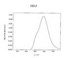
- FIG. 3is a characteristic diagram showing relative intensity in a light source in such a state that excitation energy has been switched off;
- FIG. 4is a cross-sectional view of a light emitting device in a first embodiment
- FIG. 5is a diagram showing the layer construction of an LED element in a first embodiment
- FIG. 6is a diagram showing another layer construction of the LED element in the first embodiment
- FIG. 7is a diagram showing a light emitting device in a second embodiment, wherein (a) is a longitudinal sectional view and (b) is a partially enlarged view of an LED element;
- FIG. 8is a cross-sectional view of a light emitting device in a third embodiment
- FIG. 9is a cross-sectional view of a light emitting device in a fourth embodiment.
- FIG. 10is a cross-sectional view of a light emitting device in a fifth embodiment
- FIG. 11is a cross-sectional view of a light emitting device in a sixth embodiment.
- FIG. 12is a cross-sectional view of a liquid crystal backlight device as an optical device in a seventh embodiment.
- Table 1 on line 1a luminous body having a composition (Ba 0.9648 Sr 0.01 Eu 0.025 Dy 0.0002 ) 2 (Si 0.98 Ge 0.02 ) 3 O 8.0006 is described.
- Raw materials for this luminous bodyare BaCO 3 , SrCO 3 , Eu 2 O 3 , Dy 2 O 3 , SiO 2 , and GeO 2 .
- the raw materials in an oxide form or the raw materials from materials convertible to oxidesare stoichiometrically weighed as specified in the table and mixed together, and, depending upon reaction conditions, the mixture is fired in a corundum crucible in a reducing atmosphere of a nitrogen/hydrogen mixture at 1220° C. for 4 hr.
- the final productis washed with water, is dried, and is sieved.
- the luminous body compound thus obtainedhas a maximum light emission at a color wavelength of 487 nm and has a prolonged fluorescence lifetime.
- the raw materialsare stoichiometrically weighed and vigorously mixed together for a few hours, and the mixture is then fired in a corundum crucible in a reducing atmosphere of a nitrogen/hydrogen mixture at 1245° C. for 3 hr.
- the fired cakeis ground, is washed with water, is dried, and is sieved.
- the luminous body compound thus obtainedhas a maximum light emission at a color wavelength of 589 nm and has a prolonged fluorescence lifetime.
- the raw materialsare stoichiometrically weighed and mixed together homogeneously for a few hours, and the mixture is placed in an oven at room temperature and is fired in a reducing atmosphere of a nitrogen/hydrogen mixture at 1220° C. for 4 hr.
- the fired productis ground, is washed with water, is dried, and is sieved.
- the luminous body compound thus obtainedhas a maximum light emission at a color wavelength of 509 nm and has a prolonged fluorescence lifetime.
- Table 1 on line 4a luminous body having a composition (Ba 0.0905 Sr 0.07 Zn 0.005 Mg 0.005 Eu 0.015 ) 2 Si (Al 0.0001 Dy 0.0002 )O 4.00045 is described.
- Raw materials for this luminous bodyare BaCO 3 , SrCO 3 , ZnO, Eu 2 O 3 , SiO 2 , Dy 2 O 3 , and Al 2 O 3 .
- the indicated raw materialsare mixed together at the above stoichiometrical ratio.
- the mixtureis prefired under reducing conditions at a temperature of 1220° C.
- the prefired productis ground and is then subjected to a secondary firing process in a reducing atmosphere of a nitrogen/hydrogen mixture at 1220° C.
- the secondary firing for 2 hrprovides a homogeneous final product.
- the final productis washed with water, is dried, and is sieved.
- the luminous body compound thus obtainedhas a maximum light emission at a color wavelength of 445 nm and has a prolonged fluorescence lifetime.
- a luminous body having a composition (Ba 0.915 Sr 0.005 Zn 0.005 Eu 0.075 ) 3 Mg 0.99 Mn 0.01 (Si 0.998 Ge 0.002 ) 2 (Ga 0.0001 Dy 0.0001 )O 8.0003is described.
- Raw materials for this luminous bodyare BaCO 3 , SrCO 3 , ZnO, Eu 2 O 3 , MgO, MnCO 3 , SiO 2 , GeO 2 , Dy 2 O 3 , and Ga 2 O 3 .
- the raw materialsare satisfactorily mixed, and the mixture is then subjected to a firing process.
- the firing processis carried out under reaction conditions in a reducing atmosphere of a nitrogen/hydrogen mixture at 1225° C. for 3 hr.
- the final productis ground, is washed with water, is dried, and is sieved.
- the luminous body compound thus obtainedhas a maximum light emission at a color wavelength of 543 nm and has a prolonged fluorescence lifetime.
- a luminous body having a composition (Ba 0.92 Sr 0.04 Zn 0.01 Ca 0.01 Eu 0.02 ) 2 Mg(Si 0.9 Ge 0.1 ) 2 (Ga 0.0001 Dy 0.0002 )O 7.00045is described.
- Raw materials for this luminous bodyare BaCO 3 , SrCO 3 , ZnO, CaCO 3 , Eu 2 O 3 , MgO, SiO 2 , GeO 2 , Dy 2 O 3 , and Ga 2 O 3 .
- the raw materialsare stoichiometrically weighed and are mixed together thoroughly and vigorously, and the mixture is then subjected to a firing process in a reducing atmosphere of a nitrogen/hydrogen mixture at 1235° C. for 4 hr.
- the final productis ground, is washed with water, is dried, and is sieved.
- the luminous body compound thus obtainedhas a maximum light emission at a color wavelength of 548 nm and has a prolonged fluorescence lifetime.
- a luminous body having a composition (Ba 0.8 K 0.05 Dy 0.05 Eu 0.1 ) Mg 2 Al 16 O 27is described.
- Raw materials for this luminous bodyare BaCO 3 , K 2 CO 3 , Dy 2 O 3 , Eu 2 O 3 , MgO, and Al 2 O 3 .
- the raw materialsare stoichiometrically weighed, and AlF 3 is then added as a fluxing agent, and the mixture is fired in a reducing atmosphere of a nitrogen/hydrogen mixture at 1420° C. for 2 hr.
- the fired product thus obtainedis ground, is washed several times with water, is dried, and is sieved.
- the luminous body compound thus obtainedhas a maximum light emission at a color wavelength of 452 nm and has a prolonged fluorescence lifetime.
- the relationship between the relative light emission intensity (relative intensity) and the heating temperature in the range of 100 K to 900 K for the luminous body (Ba 0.8 K 0.05 Dy 0.05 Eu 0.1 )Mg 2 Al 16 O 27is shown in FIG. 1 .
- the relative intensity of the luminous bodyis more than 0.8 in the temperature range of 200 K to about 600 K.
- Table 1 on line 8a luminous body having a composition (Ba 0.15 Sr 0.8 Eu 0.05 ) 4 Al 12.5 Ga 1.49996 Dy 0.00004 Si 0.005 O 25.0075 is described.
- Raw materials for this luminous bodyare BaCO 3 , SrCO 3 , Eu 2 O 3 , Al 2 O 3 , Ga 2 O 3 , SiO 2 , and Dy 2 O 3 .
- the indicated raw materialsare stoichiometrically weighed, and boric acid is then added as a fluxing agent, followed by mixing to prepare a homogeneous mixture.
- the mixtureis fired in a corundum crucible in a reducing atmosphere of a nitrogen/hydrogen mixture at 1420° C. for 2 hr. Subsequently, the fired product thus obtained is ground, is again mixed vigorously, and is further subjected to a firing process under the same conditions. Next, the final product thus obtained is ground, is washed with water, is dried, and is sieved.
- the luminous body compound thus obtainedhas a maximum light emission at a color wavelength of 496 nm and has a prolonged fluorescence lifetime.
- the raw materialsare stoichiometrically weighed and are mixed with boric acid and ammonium chloride as a fluxing agent, and the mixture is fired in a reducing atmosphere of a nitrogen/hydrogen mixture at 1420° C. for 2 hr.
- the fired cakeis ground and is mixed, and the firing process is then repeated.
- the final product thus obtainedis ground, is washed with water, is dried, and is sieved.
- the compound thus obtainedhas a maximum light emission at a color wavelength of 523 nm and has a prolonged fluorescence lifetime.
- FIG. 2shows a light emission spectrum of a rainbow color emitted from a light source 1 (not shown).
- the light source 1contains a mixture of the following luminous bodies:
- the relative light emission intensity (relative intensity) of color at an ultraviolet wavelength of 380 nmis 0.04, the relative light emission intensity of blue at a wavelength of 490 nm is 0.034, the relative light emission intensity of green at a wavelength of 508 nm is 0.02, the relative light emission intensity of yellow at a wavelength of 560 nm is 0.024, and the relative light emission intensity of red at a wavelength of 610 nm is 0.02.
- this light sourceEven after the excitation energy in the light source 1 is switched off, this light source still emits yellow light at a relative light emission intensity (relative intensity) of 0.0375 with a maximum luminous color wavelength of 580 nm shown in FIG. 3 .
- At least one coactivatorselected from the group consisting of lanthanum (La), cerium (Ce), praseodymium (Pr), neodymium (Nd), samarium (Sm), gadolinium (Gd), terbium (Tb), dysprosium (Dy), holmium (Ho), erbium (Er), thulium (Tm), ytterbium (Yb), lutetium (Lu), bismuth (Bi), tin (Sn), antimony (Sb) and analogues thereof is used.
- the coactivatorprovides a further center in the luminous body.
- the additional activationis advantageous in that the fluorescence lifetime can be increased to a few seconds or a few minutes or up to a few hours. This makes it possible for light sources, which are becoming more and more important especially in applications where work is performed under safe light and health light conditions, to be compatible with the behavior of the human's eye.
- the mixture of these luminous bodiesis suitable for realizing various fluorescence lifetimes. According to the invention, by virtue of this, the color of light emitted from LED can be changed upon switching-off of the excitation of the luminous body.
- the further and new centerhave an additional advantage that electrons are mainly captured from the excited state by virtue of these centers which, as a general rule, can cause radiation recombination with luminous ions.
- these electronsare not trapped by killer centers, that is, centers where excitation energy is wastefully converted to heat resulting in light emission loss.
- a luminous bodywhich comprises silicate-germanate and is improved in thermostability and fluorescence lifetime by doping with europium, wherein said luminous body further comprises an additional dopant and corresponds to the empirical formula: M′ a M′′ b (Si 1-z Ge) c (Al,Ga,In) d (Sb,V,Nb,Ta) e O (a+b+2c+3d/2+5e/2 ⁇ n/2) X n :Eu x ,R y wherein
- M′represents one or more elements selected from the group consisting of calcium (Ca), strontium (Sr), barium (Ba), and zinc (Zn);
- M′′represents one or more elements selected from the group consisting of magnesium (Mg), cadmium (Cd), manganese (Mn), and beryllium (Be);
- Rrepresents one or more elements selected from the group consisting of La, Ce, Pr, Nd, Sm, Gd, Tb, Dy, Ho, Er, Tm, Yb, Lu, Bi, Sn, and Sb;
- Xrepresents an ion selected from the group consisting of fluorine (F), chlorine (Cl), and bromine (Br) to balance the charge;
- thermostability and fluorescence lifetime in the luminous body comprising aluminate-gallate and doped with europiumcan be achieved by the luminous body that comprises an additional dopant and corresponds to the empirical formula: M′ 4 (Al,Ga) 14 (Si,Ge) p O 25+2p :Eu x ,R y or that comprises an additional dopant and corresponds to the empirical formula: M′(Al,Ga) 2 (Si,Ge) p O 4+2p :Eu x ,R y wherein
- M′represents one or more elements selected from the group consisting of Sr, Ba, Ca, Mg, and Zn;
- Rrepresents one or more elements selected from the group consisting of La, Ce, Pr, Nd, Sm, Gd, Tb, Dy, Ho, Er, Tm, Yb, Lu, Bi, Sn, and Sb;
- thermostability and fluorescence lifetime in the luminous body comprising aluminate and doped with europiumcan be achieved by the luminous body that comprises an additional dopant and corresponds to the empirical formula: (M′,M′′,M′′′)M′′′′ 2 Al 16 O 27 :Eu x ,R y wherein
- M′represents one or more elements selected from the group consisting of Ba, Sr, and Ca;
- M′′represents one or more elements selected from the group consisting of lithium (Li), sodium (Na), potassium (K), and rubidium (Rb);
- M′′′′represents Mg or Mn
- Rrepresents one or more elements selected from the group consisting of La, Ce, Pr, Nd, Sm, Gd, Tb, Ho, Er, Tm, Yb, Lu, Bi, Sn, and Sb;
- M′represents one or more elements selected from the group consisting of Ca, Sr, Ba, and Mg;
- Rrepresents one or more elements selected from the group consisting of La, Ce, Pr, Nd, Sm, Gd, Tb, Dy, Ho, Er, Tm, Yb, Lu, Bi, Sn, and Sb;
- these luminous bodiesfor example,
- the luminous body mixturecomprising a silicate-germanate luminous body according to the invention and/or the luminous body mixture comprising at least one aluminate-gallate luminous body according to the invention are also suitable as layers for improving thermostability and fluorescence lifetime in LEDs and compact energy saving lamps.
- An additional advantageis that, upon the operation of LED, electrons become free from these centers by heat energy provided by the chip per se and, at the same time, light emission can take place. In any case, generated heat is effectively converted.
- thermostability of the luminous bodycontributes to an improvement in thermostability of the luminous body and thus can be advantageously used in luminous elements and is also advantageous for use in specific LEDs which produce colored light and/or white light.
- the operation of LED at a temperature of about 60 to 120° C.can improve effectiveness over the conventional luminous body.
- the luminous body according to the inventionhas longer fluorescence lifetime than the conventional luminous body for LEDs which generally has a fluorescence lifetime on the order of microseconds.
- the silicate-germanate luminous bodyis very suitable for light emission from a blue spectrum region so far as an orange-red spectrum region in a visible spectrum depends upon the composition.
- the silicate-germanate luminous bodyhas a prolonged fluorescence lifetime and, at the same time, is selected for use as a converting material for a blue and/or ultraviolet excitation light source (wavelength 300 to 500 nm) to provide white light having a high level of effectiveness.
- a further advantageis that freeing of electrons from the centers enables an excited state other than the ordinarily existing excited state to be provided and, in some cases, upon the operation of the excitation source, the effectiveness increases with an increase in temperature.
- This principlecan be applied to luminous bodies which emit blue to red spectrum region.
- silicate-germanate luminous bodywhen used alone or in combination with an aluminate-gallate luminous body or other luminous body, upon excitation by blue and/or ultraviolet LED, colored light or white light having a prolonged fluorescence lifetime can be provided.
- Both germanium in a silicate lattice and gallium in an aluminate latticeslightly cause lattice expansion. In both the cases, emitted light is slightly shifted, and this affects the fluorescence lifetime.
- the light thus obtainedhas significantly high fluorescence lifetime, high thermostability, and high light quality.
- FIG. 4is a cross-sectional view showing a light emitting device in the first embodiment of the invention.
- This light emitting device 1is a wavelength conversion-type light emitting device 1 comprising an LED element mounted on a lead.
- This device 1includes leads 2 and 3 as wiring conductors.
- a cup part 4 for receiving an LED elementis provided on the lead 2 .
- An LED element 6is bonded to the cup part 4 in its bottom part 5 .
- the leads 2 and 3are electrically connected to electrodes (not shown) of the EL element 6 through wires 7 of gold (Au).
- the cup part 4together with the LED element 6 and the wire 7 , is sealed with a light transparent sealing resin 8 .
- a luminous body 9is mixed in the sealing resin 8 .
- the leads 2 and 3 , the LED element 6 , and the wires 7are integrally sealed with a light transparent and shell-shaped sealing resin 10 .
- the leads 2 and 3are formed of copper or a copper alloy having excellent thermal conductivity and electrical conductivity.
- the cup part 4 provided on the lead 3has an inclined inner wall formed by enlarging the size of the inner wall toward the light emitting side from the viewpoint of enhancing light emission toward the outside of the cup.
- the LED element 6is a GaN based LED element that emits blue light with wavelength 460 nm.
- the LED element 6is bonded and fixed onto the cup part 4 in its bottom 5 with the aid of a light reflective adhesive.
- the sealing resin 8is a silicone resin mixed with the luminous body 9 and has been potted in the cup part 4 for sealing of the LED element 6 .
- At least one coactivatorselected from the group consisting of lanthanum (La), cerium (Ce), praseodymium (Pr), neodymium (Nd), samarium (Sm), gadolinium (Gd), terbium (Tb), dysprosium (Dy), holmium (Ho), erbium (Er), thulium (Tm), ytterbium (Yb), lutetium (Lu), bismuth (Bi), tin (Sn), antimony (Sb) and analogues thereof is used.
- Lalanthanum
- Cecerium
- Prpraseodymium
- Ndneodymium
- Smsamarium
- Gdgadolinium
- Tbterbium
- Dydysprosium
- Hoholmium
- Ererbium
- Tmthulium
- Ybytterbium
- Lubismuth
- Bi
- the sealing resin 8has been mixed with a luminous body 9 comprising silicate-germanate and doped with europium, wherein the luminous body 9 further comprises an additional dopant and corresponds to the empirical formula: M′ a M′′ b (Si 1-z Ge z ) c (Al,Ga,In) d (Sb,V,Nb,Ta) e O (a+b+2c+3d/2+5e/2 ⁇ n/2) X n :Eu x ,R y wherein
- M′represents one or more elements selected from the group consisting of calcium (Ca), strontium (Sr), barium (Ba), and zinc (Zn);
- M′′represents one or more elements selected from the group consisting of magnesium (Mg), cadmium (Cd), manganese (Mn), and beryllium (Be);
- Rrepresents one or more elements selected from the group consisting of La, Ce, Pr, Nd, Sm, Gd, Tb, Dy, Ho, Er, Tm, Yb, Lu, Bi, Sn, and Sb;
- Xrepresents an ion selected from the group consisting of fluorine (F), chlorine (Cl), and bromine (Br) to balance the charge;
- the sealing resin 10is an epoxy resin and has a hemispherical optical shape on the light emission side formed by casting molding using a mold for forming a shell shape.
- FIG. 5is a diagram showing the layer construction of the LED element 6 .
- the LED element 6includes a sapphire substrate 61 .
- An AlN buffer layer 62is provided on the sapphire substrate 61 .
- An Si-doped n-type GaN cladding layer (a contact layer) 63is provided on the AlN buffer layer 62 .
- MQW 64is provided on the n-type GaN cladding layer 63 .
- MQW 64comprises, provided on the n-type GaN cladding layer 63 , three InGaN well layers 64 A alternating with two GaN barrier layers 64 B.
- An Mg-doped p-type GaN cladding layer 65is provided on MQW 64 .
- An Mg-doped p-type GaN contact layer 66is provided on the p-type GaN cladding layer 65 .
- a transparent electrode 67is provided on the p-type GaN contact layer 66 .
- a pad electrode 68is provided on the transparent electrode 67 at its predetermined position, for example, a position near the side face of the element.
- the LED element 6further includes an n-side electrode 69 which is formed by removing a part of the p-type GaN contact layer 66 , the p-type GaN cladding layer 65 , MQW 64 , and the n-type GaN cladding layer 63 by etching to expose the n-type GaN cladding layer 63 and forming the n-side electrode 69 on the exposed n-type GaN cladding layer 63 .
- This LED element 6has a double heterostructure having MQW 64 as a luminous layer, and Al may be properly incorporated in each layer.
- a copper plate for a lead frameis punched by pressing to form a lead frame with leads 2 and 3 .
- the cup part 4may be formed on the lead 3 in the formation of the lead frame.
- the LED element 6is then bonded and fixed onto a position within the cup part 4 with the aid of an adhesive.
- the pad electrode 68 in the LED element 6is electrically connected to the lead 2 through the wire 7
- the n-side electrode 69is electrically connected to the lead 3 through the wire 7 .
- a silicone resin previously mixed with the luminous body 9is then potted in the cup part 4 to seal the LED element 6 .
- the leads 2 and 3 with the sealed LED element 6are then placed in a resin molding mold. An epoxy resin is then poured into the mold to form a shell-shaped sealing resin 10 around the leads 2 and 3 .
- the leads 2 and 3are then cut from the lead frame.
- the leads 2 and 3are connected to a power supply unit (not shown).
- a power supply unitnot shown.
- light emissiontakes place in MQW 64 in the LED element 6 .
- Light based on the light emission in MQW 64is emitted to the outside of the LED element 6 , whereby the luminous body 9 is irradiated with this light.
- the luminous body 9is excited by the light emitted from the LED element 6 (hereinafter referred to as “emitted light”) to emit excitation light.
- the emitted light and the excitation lightare mixed together to produce white light within the cup part 4 .
- This white lightis emitted from the inside of the cup part 4 to the outside of the light emitting device through the sealing resin 10 .
- a part of the white lightis reflected from the inclined inner wall in the cup part 4 and is then emitted to the outside of the light emitting device 1 through the sealing resin 10 .
- the cup part 4is sealed with the sealing resin 8 mixed with the luminous body 9 comprising the conventional activator and the additional coactivator.
- This constructioncan improve the thermostability of the luminous body and can suppress the shift of light emission energy distribution to stabilize the color of light emitted from the LED element 6 .
- the addition of the coactivatorcan prolong the fluorescence lifetime to a few seconds or a few minutes or up to a few hours. Therefore, the light emitting device 1 is very suitable for use in applications where work is performed under safe light and health light conditions, to be compatible with the behavior of the human's eye.
- the addition of the coactivatorcan realize various fluorescence lifetimes. Therefore, the color of light emitted from the light emitting device 1 can be changed upon switching-off of the excitation of the luminous body.
- the luminous body 9may be used as a mixture with other luminous body.
- Other luminous bodies usable hereininclude, for example, YAG.
- YAGa luminous body
- a construction using a combination of a light emitting device comprising a blue LED element and YAG with the luminous body 9 and a construction using a combination of a light emitting device comprising an ultraviolet LED element and a luminous body excitable by ultraviolet light with the luminous body 9may be adopted.
- the construction in which the luminous body 9 comprising silicate-germanate and doped with europium and further comprising the above additional dopant is mixed in the sealing resin 8has been explained.
- the following luminous bodymay be mixed as other luminous body 9 : a luminous body 9 that comprises aluminate-gallate and doped with europium, wherein the luminous body further comprises an additional dopant and corresponds to the empirical formula: M′ 4 (Al,Ga) 14 (Si,Ge) p O 25+2p :Eu x ,R y or wherein the luminous body further comprises an additional dopant and corresponds to the empirical formula: M′(Al,Ga) 2 (Si,Ge)O 4+2p :Eu x ,R y wherein
- M′represents one or more elements selected from the group consisting of Sr, Ba, Ca, Mg, and Zn;
- Rrepresents one or more elements selected from the group consisting of La, Ce, Pr, Nd, Sm, Gd, Tb, Dy, Ho, Er, Tm, Yb, Lu, Bi, Sn, and Sb;
- the following luminous bodymay be mixed as other luminous body 9 : a luminous body 9 that comprises aluminate and doped with europium, wherein the luminous body further comprises an additional dopant and corresponds to the empirical formula: (M′,M′′,M′′′)M′′′′ 2 Al 16 O 27 :Eu x ,R y wherein
- M′represents one or more elements selected from the group consisting of Ba, Sr, and Ca;
- M′′represents one or more elements selected from the group consisting of lithium (Li), sodium (Na), potassium (K), and rubidium (Rb);
- M′′′′represents Mg or Mn
- Rrepresents one or more elements selected from the group consisting of La, Ce, Pr, Nd, Sm, Gd, Tb, Ho, Er, Tm, Yb, Lu, Bi, Sn, and Sb;
- the following luminous bodymay be mixed as other luminous body 9 : a luminous body 9 that comprises alkaline earth metal aluminate-gallate and doped with europium, wherein the luminous body further comprises an additional dopant and corresponds to the empirical formula: M′ 1-a (Al,Ga) b (Si,Ge) c O 1.5b+1+3c/2 :Eu x ,R y wherein
- M′represents one or more elements selected from the group consisting of Ca, Sr, Ba, and Mg;
- Rrepresents one or more elements selected from the group consisting of La, Ce, Pr, Nd, Sm, Gd, Tb, Dy, Ho, Er, Tm, Yb, Lu, Bi, Sn, and Sb;
- luminous bodiesprovided by combining the above luminous bodies, for example,
- a light reflective layermay be provided on MQW 64 in its sapphire substrate 61 side.
- an Al layermay be provided as the light reflective layer on the sapphire substrate 61 .
- FIG. 6is a diagram showing another embodiment of the layer construction of the LED element 6 .
- This LED element 6is the same as the LED element 6 shown in FIG. 5 , except that a GaN substrate 70 is used as the substrate and the provision of the AlN buffer layer is omitted.
- An LED element 6 formed by performing crystal growth of a GaN base semiconductor layer on the GaN substrate 70may also be used. Further, an LED element 6 using a substrate formed of a material such as Si, SiC, or AlGaN may be used as a light source.
- FIG. 7shows a light emitting device in the second embodiment of the invention, wherein (a) is a longitudinal sectional view and (b) is a partially enlarged view of an LED element. Parts corresponding to the respective parts in the first embodiment are identified with the same reference numerals.
- the light emitting device 1includes an LED element 11 .
- a submount part 13 formed of Siis electrically connected through Au bumps 12 A and 12 B to the LED element 11 .
- An Ag paste 14 as an electrically conductive adhesiveelectrically connects the submount part 13 to a lead 15 A in its cup part 15 a .
- a lead 15 Bis electrically connected to the submount part 13 through a wire.
- An element receiving part 15 Cis provided in the lead 15 A.
- An inclined light reflective surface 15 bis provided within the element receiving part 15 C.
- the LED element 11includes a light transparent sapphire substrate 110 .
- a light transparent sapphire substrate 110On the substrate 110 are provided, in the following order, an AlN buffer layer 111 , an n-type GaN cladding layer 112 , MQW 113 comprising three InGaN well layers alternating with two GaN barrier layers, a p-type GaN cladding layer 114 , and a p-type GaN contact layer 115 .
- the LED element 11further includes an n-side electrode 116 which is formed by removing a part of the p-type GaN contact layer 115 , the p-type GaN cladding layer 114 , MQW 113 , and the n-type GaN cladding layer 112 by etching to expose the n-type GaN cladding layer 112 and forming the n-side electrode 116 on the exposed n-type GaN cladding layer 112 .
- a p-side electrode 117is provided on the p-type GaN contact layer 115 .
- the LED element 11is fixed to the submount part 13 so that the substrate side is disposed on the opening side of the cup part 15 a.
- the submount part 13includes an n-type semiconductor layer 134 .
- An n-side electrode 130is provided on the surface of the n-type semiconductor layer 134 .
- a p-type semiconductor layer 131is provided on a part of the n-type semiconductor layer 134 .
- a p-side electrode 132i's provided on the p-type semiconductor layer 131 .
- An n-side electrode 133is provided on the n-type semiconductor layer 134 in its bottom side, that is, in its side where the n-type semiconductor layer 134 is bonded to the cup part 15 a .
- the n-side electrode 130is connected to the p-side electrode 117 in the LED element 11 through the Au bump 12 A.
- the p-side electrode 132is connected through the Au bump 12 B to the n-side electrode 116 in the LED element 11 , and the wire 7 is connected to the p-side electrode 132 .
- the sealing resin 8has been mixed with the luminous body 9 explained in connection with the first embodiment and has been potted into the cup part 15 a so as to cover the LED element 11 and the submount part 13 for sealing.
- an Ag paste 14is first coated onto the cup part 15 a in its bottom part 15 c .
- the submount part 13is then fixed to the position within the cup part 15 a by the Ag paste 14 .
- the LED element 11is mounted through the Au bumps 12 A and 12 B.
- the LED element 11is bonded to the submount part 13 by ultrasonic bonding.
- the p-side electrode 132is then electrically connected to the lead 15 B through the wire.
- the sealing resin 8is then potted in the cup part 15 a to cover the LED element 11 and the submount 13 for sealing.
- the sealing resin 10is molded into a shell shape to seal the lead 15 A with the sealed cup part 15 a and the lead 15 B.
- the light emitting device 1 in the second embodimentis advantageous in that, in addition to the favorable effects of the first embodiment, an additional effect, that is, the effect of improving light takeout efficiency, can be attained by virtue of the construction in which light based on light emission in MQW 113 can be emitted from the sapphire substrate side. Further, the function of protection against static electricity can be imparted to the submount part 13 . In this case, breaking of the LED element 11 by static electricity can be prevented.
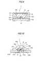
- FIG. 8is a cross-sectional view showing a light emitting device in the third embodiment of the invention.
- this light emitting device 1is such that a cap-shaped luminous body layer 18 formed of a resin material such as an epoxy resin containing the luminous body 9 explained above in connection with the first and second embodiments is provided on the surface of the shell-shaped sealing resin 10 , and the luminous body 9 has been omitted from the sealing resin 8 for sealing the cup part 15 a.
- a resin materialsuch as an epoxy resin containing the luminous body 9 explained above in connection with the first and second embodiments
- the light emitting device 1 in the third embodimentis advantageous in that, in addition to the favorable effects of the first and second embodiments, an additional effect can be attained. Specifically, since the luminous body 9 is not deposited around the LED element 11 , a lowering in efficiency of emission to the outside of the light emitting device caused by the absorption of light in the deposited phosphor can be prevented. By virtue of this effect, light efficiently led to the surface of the sealing resin 10 can be subjected to wavelength conversion in the luminous body layer 18 , followed by emission to the outside to the light emitting device. Thus, a high-brightness wavelength conversion-type light emitting device 1 can be provided.
- FIG. 9is a cross-sectional view showing a light emitting device in the fourth embodiment of the invention.
- parts corresponding to the respective parts in the first to third embodimentsare identified with the same reference numerals.
- This light emitting device 1is a surface mounting-type wavelength conversion-type light emitting device 1 .
- the light emitting device 1includes an LED element 11 , a wavelength converting part 19 including a luminous body layer 18 excitable based on light emitted from the LED element 11 , a body 20 formed of a resin material such as an acrylic resin, and a ceramic substrate 21 for mounting thereon the LED element 11 .
- Wavelength converting part 19is formed by interposing a luminous body layer 18 formed of the luminous body 9 explained above in connection with the first to third embodiments between two glass sheets formed of low melting glass and heating the assembly for integration.
- the luminous body 9is screen printed on one side of the first glass sheet, and the printed first glass sheet is heat treated at 150° C. to remove the binder component to form a thinned film.
- the second glass sheetis disposed so that the thinned luminous body layer 18 is interposed between the first and second glass sheets, followed by heat treatment to integrate the first and second glass sheets.
- the body 20has a light reflective surface 15 b in its inner part.
- the light reflective surface 15 breflects light emitted from the LED element 11 toward the wavelength converting part 19 .
- the light emitting surface and the surface of the wavelength converting part 19constitute an identical plane.
- a space surrounded by the light reflective surface 15 bis filled with a silicone resin 16 .
- the ceramic substrate 21has on its surface wiring layers 21 A and 21 B in a copper foil pattern for joining the LED element 11 to the ceramic substrate 21 through the Au bumps 12 A and 12 B.
- the wiring layers 21 A and 21 Bare provided through the side face of the ceramic substrate 21 toward the backside, of the ceramic substrate 21 , which is a surface for joining to an external circuit.
- the light emitting device 1 in the fourth embodiment of the inventionis advantageous in that, in addition to the favorable effects of the first to third embodiments, an additional effect can be attained. Specifically, since the thin-film luminous body layer 18 formed of the luminous body 9 is sealed with glass, the water resistance and moisture absorption resistance of the phosphor layer 18 can be improved. Thus, a light emitting device 1 which exhibits good wavelength conversion for a long period of time can be provided.
- the luminous body layer 18is formed in a thin film form based on screen printing and heat treatment. Therefore, light absorption loss caused by the luminous body layer 18 can be reduced, and, thus, a high-brightness wavelength conversion-type light emitting device 1 can be realized.
- the amount of the luminous body 9 usedcan be reduced. Therefore, a cost reduction in the light emitting device 1 can be realized.
- FIG. 10is a cross-sectional view showing a light emitting device in the fifth embodiment of the invention.
- parts corresponding to the respective parts in the first to fourth embodimentsare identified with the same reference numerals.
- This light emitting device 1includes a flip chip-type (0.3 ⁇ 0.3 mm) LED element 11 .
- the LED element 11is mounted on a submount part 13 of AlN.
- Lead frames 22 A and 22 Bare joined to the submount part 13 .
- a wavelength converting part 19 formed of low melting glassis provided for sealing the LED element 11 and the submount part 13 and for performing wavelength conversion of light emitted from the LED element 11 .
- the submount part 13 and the lead frames 22 A and 22 B, together with the wavelength converting part 19are integrally sealed by a glass sealing part 23 formed of low melting glass.
- the wavelength converting part 19has an optical shape which can regulate the distribution of light emitted from the LED element 11 , that is, is formed in a dome form, and, further, comprises a luminous body layer 18 disposed apart by a predetermined distance from the LED element 11 .
- Wiring layers 21 A and 21 B formed of a copper foilare provided on the surface of the submount part 13 .
- the wiring layers 21 A and 21 Bare electrically connected to the lead frames 22 A and 22 B by fitting into stepped parts 22 a and 22 b provided in the lead frames 22 A and 22 B.
- the optical shapeis formed by interposing the luminous body layer 18 between the first and second glass sheets explained above in connection with the fourth embodiment and hot pressing the assembly. Further, the lead frames 22 A and 22 B are integrally sealed by heat treatment of a third glass sheet for constituting the glass sealing part 23 simultaneously with the hot pressing.
- the luminous body layer 18is disposed while providing a spacing, corresponding to the thickness of the glass sheet upon deformation based on the heat treatment of the glass, between the luminous body layer 18 and the LED element 11 .
- the light emitting device 1 in the fifth embodiment of the inventionis advantageous in that, in addition to the favorable effects of the first to fourth embodiments, an additional effect can be attained. Specifically, since the wavelength converting part 19 has an optical shape, light produced by mixing light emitted from the LED element 11 with light subjected to wavelength conversion in the luminous body layer 18 can be emitted to a desired area.
- sealing of the LED element 11 with glasscan improve water resistance and moisture absorption resistance.
- a high-brightness wavelength conversion-type light emitting device 1which is stable even under severe environmental conditions such as high-humidity conditions for a long period, can be realized.
- FIG. 11is a cross-sectional view showing a light emitting device in the sixth embodiment of the invention.
- parts corresponding to the respective parts in the first to fifth embodimentsare identified with the same reference numerals.
- a ceramic substrate 21 having on its both sides wiring layers 24 A, 24 B, 25 A, and 25 B formed of a copper foilis used, and the wiring layer 24 A is electrically connected to the wiring layer 25 A through a through-hole 26 while the wiring layer 24 B is electrically connected to the wiring layer 25 B through a through-hole 26 .
- a flip chip-type (1 ⁇ 1 mm) LED element 11is electrically connected to the wiring layers 24 A, 24 B respectively through Au bumps 12 A and 12 B.
- the wiring layers 24 A and 24 Bare formed so as to have a larger area than the area of bonding of the glass material constituting the wavelength converting part 19 .
- the light emitting device 1 in the sixth embodiment of the inventionis advantageous in that, in addition to the favorable effects of the first to fifth embodiments, an additional effect can be attained. Specifically, since the wavelength converting part 19 is bonded to the wiring layers 24 A and 24 B formed of a copper foil provided on the surface of the ceramic substrate 21 , excellent adhesion between the wavelength converting part 19 and the wiring layers 24 A and 24 B can be achieved based on good adhesion between the glass material and the copper foil. By virtue of this, separation of the wavelength converting part 19 and absorption of moisture in the interior of the light emitting device 1 can be firmly prevented. Thus, a highly reliable wavelength conversion-type light emitting device 1 can be realized.
- the ceramic substrate 21since the ceramic substrate 21 is used, a group of light emitting devices which have been formed together on a substrate material as a base can easily be taken off by cutting such as dicing or scribing. Thus, a wavelength conversion-type light emitting device 1 can be manufactured with high productivity.
- FIG. 12is a cross-sectional view showing a liquid crystal backlight device as an optical device in the seventh embodiment of the invention.
- parts corresponding to the respective parts in the first to sixth embodimentsare identified with the same reference numerals.
- This liquid crystal backlight device 30includes an LED lamp 31 as a light source, and a light guide body 32 for guiding light emitted from the LED lamp.
- a luminous body layer 18 for performing wavelength conversion of light emitted from the LED lamp 31is provided on a surface of the light guide body 32 .
- a liquid crystal panel 35is provided for permitting the transmission of light from the back surface based on the wavelength converted light.
- the LED lamp 31functions to collect, in a shell-shaped resin sealing part, blue light with wavelength 460 nm based on light emission in an LED element comprising a GaN based semiconductor layer and to emit the collected light to a predetermined radiation area.
- the light guide body 32has a reflecting surface 32 A for reflecting light supplied from the LED lamp 31 in a right-angle direction, a bottom surface 32 B, and an inclined surface 32 C to which the light, which has been reflected from the reflecting surface 32 A and guided through the light guide body 32 , is incident.
- a light reflective layer 33is provided on the bottom surface 32 B.
- a luminous body layer 18 formed of a luminous body comprising a conventional activator and, in addition, at least one coactivator selected from La, Ce, Pr, Nd, Sm, Gd, Tb, Dy, Ho, Er, Tm, Yb, Lu, Bi, Sn, Sb, and analogues thereofis provided in a thin film form on the inclined surface 32 C.
- the liquid crystal panel 35comprises, for example, a TFT (thin film transistor) substrate, a liquid crystal layer, and a color filter substrate stacked on top of one another and is transparent to light for permitting light emitted from the light guide body 32 to be transmitted therethrough.
- TFTthin film transistor
- this liquid crystal backlight device 30light emitted from the LED lamp 31 is guided to the inclined surface 32 C through the light guide body 32 , and the light emitted from the LED lamp 31 is subjected to wavelength conversion in the luminous body layer 18 provided on the inclined surface 32 C to produce white light, which passes through the liquid crystal panel 35 for illumination.
- the liquid crystal backlight device 30 in the seventh embodiment of the inventionis advantageous in that, in addition to the favorable effects explained above in connection with the first to sixth embodiments, an additional effect can be attained.
- light guided through the light guide body 32is subjected to wavelength conversion in the luminous body layer 18 provided on the backside of the liquid crystal backlight device 30 before emission to the outside of the backlight device.
- good brightnesscan be provided using blue light as a light source.
- a transmission illumination structure with a prolonged fluorescence lifetimecan be realized, and the backlight device can impart novel visuality as an illuminator for cellular phones (portable telephones) or equipment having a liquid crystal display part.
- the fluorescence lifetime of the luminous body layer 18is so long that power saving can be realized based on a combination of the luminous body layer 18 with the regulation of light emission in the LED lamp 31 without sacrificing the light quality and the serviceable time of equipment using a power supply such as a battery can be prolonged.
- the seventh embodimentlight emitted from the LED lamp 31 is reflected from the reflecting surface 32 A, and the reflected light is then guided through the light guide body 32 .
- a construction not provided with the reflecting surface 32 Acan be adopted.
- a light incidence end face perpendicular to the bottom surface 32 Bis formed so that the direction of emitted light incident to the light guide body 32 is identical to the light guide direction.
- an LED lamp capable of emitting blue lightan LED lamp capable of emitting ultraviolet light can be used as the LED lamp 31 .
- thermostability of the luminous bodycan be improved. Therefore, a shift in light emission energy distribution is less likely to take place, and a change in a light color can be suppressed. Further, the fluorescence lifetime can be prolonged from a few microsecond order to a few seconds or a few minutes.
- thermostability and fluorescence lifetime propertiescan provide optical devices having excellent properties such as high light quality, good power saving, and high brightness.
Landscapes
- Chemical & Material Sciences (AREA)
- Inorganic Chemistry (AREA)
- Engineering & Computer Science (AREA)
- Materials Engineering (AREA)
- Organic Chemistry (AREA)
- Luminescent Compositions (AREA)
- Led Device Packages (AREA)
- Led Devices (AREA)
Abstract
Description
- This application is based on German Patent Application No. (DE10259945.9), the entire disclosures of which are incorporated herein by reference.
- The invention relates to a luminous body (or phosphor) having a prolonged fluorescence lifetime and an optical device using the same, for example, a luminous body for use in the manufacture of an optoelectronic solid constituent element and a compact energy saving lamp, and an optical device using the same.
- Butler, K. H.: “Fluorescent Lamp Phosphors in Technology and Theory”, University of Pennsylvania, Press University Park (1980) discloses luminous bodies for fluorescent lamps which can be excited in both blue and short wavelength ultraviolet spectrum regions and emit light in a visible spectrum region. However, what has been known about these luminous bodies up to now is that they can be used only in fluorescent lamps and compact energy saving lamps.
- Both organic dyes and inorganic dyes are used in LEDs. However, organic dyes, when used alone, are low in stability and are low in effectiveness.
- WO 98/12757, WO 02/93116, and U.S. Pat. No. 6,252,254 disclose inorganic materials which will be more and more used as a color converting material for producing white light. They, however, should cope with a YAG luminous body system composed mainly of yttrium aluminum garnet. This luminous body species is disadvantageous in that the white light produced is on a low color rendering level, and, for example, in the case of a combination of a blue LED with this yellow light luminous body, color rendering index Ra is 70 to 77 which belongs to color rendering species IIa. Unsatisfactory quality of the produced white light is attributable to an elliptical light distribution which can provide only unsatisfactory white light even when a color temperature below 5000 K is provided. The use of the YAG luminous body system, however, is limited to use in blue LED. For a color wavelength of less than 460 nm, the excitation of the YAG luminous body system is dramatically decreased. In a color wavelength range of 370 to 400 nm in which UVLED is operated, the YAG luminous body system can be excited only to a limited extent.
- WO 00/33389 describes a Ba2SiO4:Eu2+ luminous body system which has also good properties with stimulation in a color wavelength of less than 500 nm and exhibits maximum emission at a color wavelength of 505 nm.
- WO 00/33390 discloses a luminous body mixture for LED which provides a color temperature of 3000 to 6500 K with a simultaneous color rendering index Ra of 83 to 87. Preferably, this luminous body, when used in combination with a further luminous body capable of emitting light in a red spectrum region or a blue spectrum region, can be used as a mixture for producing colored light and/or white light. All the conventional luminous bodies used in LEDs are disadvantageously unsatisfactory in temperature characteristics, as well as in thermostability. Due to these drawbacks, during the operation of LED, the effectiveness of the luminous body significantly decreases with increasing the temperature. As with the case of the YAG luminous body system, this causes a shift in energy distribution of light emission which causes a light color change.
- For some of applications, conventional luminous bodies used in LEDs, for example, a Ce-activated YAG luminous body composed of barium magnesium aluminate and an Eu-activated BAM luminous body, have an additional drawback of a short fluorescence lifetime. The fluorescence lifetime of main conventional luminous bodies, that is, the Ce-activated luminous body and the Eu-activated luminous body, is typically a few microseconds. In some cases, the maximum fluorescence lifetime is a few milliseconds. This can be achieved, for example, by additional doping of manganese.
- It is an object of the invention to provide a luminous body (or phosphor) that has an improved thermostability and a prolonged fluorescence lifetime associated therewith.
- It is another object of the invention to provide an optical device that possesses excellent properties such as high light quality, good power saving, and high brightness.
- (A) According to one aspect of the invention, there is provided a luminous body with a prolonged fluorescence lifetime, characterized by comprising an activator and further at least one coactivator selected from the group consisting of lanthanum (La), cerium (Ce), praseodymium (Pr), neodymium (Nd), samarium (Sm), gadolinium (Gd), terbium (Tb), dysprosium (Dy), holmium (Ho), erbium (Er), thulium (Tm), ytterbium (Yb), lutetium (Lu), bismuth (Bi), tin (Sn), antimony (Sb) and analogues thereof as an additional luminescent center for enhancing the thermostability of luminous body.
- (B) According to another aspect of the invention, there is provided
- an optical device comprising a wavelength converting part comprising a luminous body which emits light upon excitation based on light emitted from an LED element,
- characterized in that said wavelength converting part comprises a luminous body comprising an activator and further at least one coactivator selected from the group consisting of lanthanum (La), cerium (Ce), praseodymium (Pr), neodymium (Nd), samarium (Sm), gadolinium (Gd), terbium (Tb), dysprosium (Dy), holmium (Ho), erbium (Er), thulium (Tm), ytterbium (Yb), lutetium (Lu), bismuth (Bi), tin (Sn), antimony (Sb) and analogues thereof as an additional luminescent center for enhancing the thermostability.
- (C) According to still another aspect of the invention, there is provided
- an optical device characterized by comprising
- an LED element,
- a power feeding part for mounting said LED element thereon and feeding power to said LED element,
- a light transparent sealing part for sealing said LED element and said power feeding part integrally with each other, and
- a wavelength converting part for emitting light upon excitation based on light emitted from said LED element, said wavelength converting part comprising a luminous body comprising an activator and further at least one coactivator selected from the group consisting of lanthanum (La), cerium (Ce), praseodymium (Pr), neodymium (Nd), samarium (Sm), gadolinium (Gd), terbium (Tb), dysprosium (Dy), holmium (Ho), erbium (Er), thulium (Tm), ytterbium (Yb), lutetium (Lu), bismuth (Bi), tin (Sn), antimony (Sb) and analogues thereof as an additional luminescent center for enhancing the thermostability.
- (D) According to a further aspect of the invention, there is provided
- an optical device characterized by comprising
- an LED lamp,
- a light guiding part for guiding light emitted from said LED lamp,
- a wavelength converting part for emitting light upon excitation based on light guided through said light guiding part, said wavelength converting part comprising a luminous body comprising an activator and further at least one coactivator selected from the group consisting of lanthanum (La), cerium (Ce), praseodymium (Pr), neodymium (Nd), samarium (Sm), gadolinium (Gd), terbium (Tb), dysprosium (Dy), holmium (Ho), erbium (Er), thulium (Tm), ytterbium (Yb), lutetium (Lu), bismuth (Bi), tin (Sn), antimony (Sb) and analogues thereof as an additional luminescent center for enhancing the thermostability, and
- a lighting part for lighting based on light emitting through said wavelength converting part.
FIG. 1 is a characteristic diagram showing the relationship between relative intensity and heating temperature for the luminous body according to the invention;FIG. 2 is a characteristic diagram showing the relationship between relative intensity and light emission spectrum for the luminous body according to the invention;FIG. 3 is a characteristic diagram showing relative intensity in a light source in such a state that excitation energy has been switched off;FIG. 4 is a cross-sectional view of a light emitting device in a first embodiment;FIG. 5 is a diagram showing the layer construction of an LED element in a first embodiment;FIG. 6 is a diagram showing another layer construction of the LED element in the first embodiment;FIG. 7 is a diagram showing a light emitting device in a second embodiment, wherein (a) is a longitudinal sectional view and (b) is a partially enlarged view of an LED element;FIG. 8 is a cross-sectional view of a light emitting device in a third embodiment;FIG. 9 is a cross-sectional view of a light emitting device in a fourth embodiment;FIG. 10 is a cross-sectional view of a light emitting device in a fifth embodiment;FIG. 11 is a cross-sectional view of a light emitting device in a sixth embodiment; andFIG. 12 is a cross-sectional view of a liquid crystal backlight device as an optical device in a seventh embodiment.- The luminous body according to the invention will be explained in more detail in conjunction with the accompanying drawings and the like.
- Some of luminous bodies according to the invention having a prolonged fluorescence lifetime, together with their relative light emission density at varied temperatures, will be shown in Table 1.
TABLE 1 Relative light emission density Composition of luminous body 25° C. 70° C. 100° C. 120° C. (Ba0.9648Sr0.01Eu0.025Dy0.0002)2(Si0.98Ge0.02)3O8.0006 100% 100.6% 102.7% 101.5% (Ba0.9696Sr0.015Ca0.005Eu0.01Pr0.0004)3(Si0.99Ge0.01)O5.0018 100% 102.4% 102.8% 102.0% (Ba0.965Sr0.02Zn0.005Eu0.01)(Si0.97Ge0.03)2(Al0.002Dy0.00003)O5.003045 100% 101.4% 102.0% 101.5% (Ba0.905Sr0.07Zn0.005Mg0.005Eu0.015)2Si(Al0.0001Dy0.0002) O 4.00045100% 101.2% 102.4% 102.3% (Ba0.915Sr0.005Zn0.005Eu0.075)3Mg0.99Mn0.01(Si0.998Ge0.002)2(Ga0.0001Dy0.0001) O 8.0003100% 102.0% 103.6% 102.4% (Ba0.92Sr0.04Zn0.01Ca0.01Eu0.02)2Mg(Si0.9Ge0.1)2(Ga0.0001Dy0.0002) O 7.00045100% 100.6% 101.0% 100.8% (Ba0.8K0.05Dy0.05Eu0.1)Mg2Al16 O 27100% 102.8% 107.4% 108.0% (Ba0.15Sr0.8Eu0.05)4Al12.5Ga1.49996Dy0.00004Si0.005O25.0075 100% 101.5% 103.5% 103.5% (Ba0.47Sr0.5Eu0.03)Al1.5997Ga0.4Dy0.0003Si0.004O4.006 100% 100.5% 100.8% 100.6% - (1) In Table 1 on
line 1, a luminous body having a composition (Ba0.9648Sr0.01Eu0.025Dy0.0002)2(Si0.98Ge0.02)3O8.0006is described. Raw materials for this luminous body are BaCO3, SrCO3, Eu2O3, Dy2O3, SiO2, and GeO2. - Preparation:
- The raw materials in an oxide form or the raw materials from materials convertible to oxides are stoichiometrically weighed as specified in the table and mixed together, and, depending upon reaction conditions, the mixture is fired in a corundum crucible in a reducing atmosphere of a nitrogen/hydrogen mixture at 1220° C. for 4 hr. The final product is washed with water, is dried, and is sieved. The luminous body compound thus obtained has a maximum light emission at a color wavelength of 487 nm and has a prolonged fluorescence lifetime.
- (2) In Table 1 on
line 2, a luminous body having a composition (Ba0.9696Sr0.015Ca0.005Eu0.01Pr0.0004)3(Si0.99Ge0.01)O5.0018is described. Raw materials for this, luminous body are BaCO3, SrCO3, CaCO3, Eu2O3, Pr6O11, SiO2, and GeO2. - Preparation:
- The raw materials are stoichiometrically weighed and vigorously mixed together for a few hours, and the mixture is then fired in a corundum crucible in a reducing atmosphere of a nitrogen/hydrogen mixture at 1245° C. for 3 hr. The fired cake is ground, is washed with water, is dried, and is sieved. The luminous body compound thus obtained has a maximum light emission at a color wavelength of 589 nm and has a prolonged fluorescence lifetime.
- (3) In Table 1 on
line 3, a luminous body having a composition (Ba0.965Sr0.02Zn0.005Eu0.01) (Si0.97Ge0.03)2(Al0.002Dy0.00003)O5.003045is described. Raw materials for this luminous body are BaCO3, SrCO3, ZnO, Eu2O3, SiO2, GeO2, Al2O3and Dy2O3. - Preparation:
- The raw materials are stoichiometrically weighed and mixed together homogeneously for a few hours, and the mixture is placed in an oven at room temperature and is fired in a reducing atmosphere of a nitrogen/hydrogen mixture at 1220° C. for 4 hr. The fired product is ground, is washed with water, is dried, and is sieved. The luminous body compound thus obtained has a maximum light emission at a color wavelength of 509 nm and has a prolonged fluorescence lifetime.
- (4) In Table 1 on
line 4, a luminous body having a composition (Ba0.0905Sr0.07Zn0.005Mg0.005Eu0.015)2Si (Al0.0001Dy0.0002)O4.00045is described. Raw materials for this luminous body are BaCO3, SrCO3, ZnO, Eu2O3, SiO2, Dy2O3, and Al2O3. - Preparation:
- The indicated raw materials are mixed together at the above stoichiometrical ratio. The mixture is prefired under reducing conditions at a temperature of 1220° C. The prefired product is ground and is then subjected to a secondary firing process in a reducing atmosphere of a nitrogen/hydrogen mixture at 1220° C. The secondary firing for 2 hr provides a homogeneous final product. Thereafter, the final product is washed with water, is dried, and is sieved. The luminous body compound thus obtained has a maximum light emission at a color wavelength of 445 nm and has a prolonged fluorescence lifetime.
- (5) In Table 1 on
line 5, a luminous body having a composition (Ba0.915Sr0.005Zn0.005Eu0.075)3Mg0.99Mn0.01(Si0.998Ge0.002)2(Ga0.0001Dy0.0001)O8.0003is described. Raw materials for this luminous body are BaCO3, SrCO3, ZnO, Eu2O3, MgO, MnCO3, SiO2, GeO2, Dy2O3, and Ga2O3. - Preparation:
- The raw materials are satisfactorily mixed, and the mixture is then subjected to a firing process. The firing process is carried out under reaction conditions in a reducing atmosphere of a nitrogen/hydrogen mixture at 1225° C. for 3 hr. The final product is ground, is washed with water, is dried, and is sieved. The luminous body compound thus obtained has a maximum light emission at a color wavelength of 543 nm and has a prolonged fluorescence lifetime.
- (6) In Table 1 on
line 6, a luminous body having a composition (Ba0.92Sr0.04Zn0.01Ca0.01Eu0.02)2Mg(Si0.9Ge0.1)2(Ga0.0001Dy0.0002)O7.00045is described. Raw materials for this luminous body are BaCO3, SrCO3, ZnO, CaCO3, Eu2O3, MgO, SiO2, GeO2, Dy2O3, and Ga2O3. - Preparation:
- The raw materials are stoichiometrically weighed and are mixed together thoroughly and vigorously, and the mixture is then subjected to a firing process in a reducing atmosphere of a nitrogen/hydrogen mixture at 1235° C. for 4 hr. The final product is ground, is washed with water, is dried, and is sieved. The luminous body compound thus obtained has a maximum light emission at a color wavelength of 548 nm and has a prolonged fluorescence lifetime.
- (7) In Table 1 on
line 7, a luminous body having a composition (Ba0.8K0.05Dy0.05Eu0.1) Mg2Al16O27is described. Raw materials for this luminous body are BaCO3, K2CO3, Dy2O3, Eu2O3, MgO, and Al2O3. - Preparation:
- The raw materials are stoichiometrically weighed, and AlF3is then added as a fluxing agent, and the mixture is fired in a reducing atmosphere of a nitrogen/hydrogen mixture at 1420° C. for 2 hr. The fired product thus obtained is ground, is washed several times with water, is dried, and is sieved. The luminous body compound thus obtained has a maximum light emission at a color wavelength of 452 nm and has a prolonged fluorescence lifetime.
- The relationship between the relative light emission intensity (relative intensity) and the heating temperature in the range of 100 K to 900 K for the luminous body (Ba0.8K0.05Dy0.05Eu0.1)Mg2Al16O27is shown in
FIG. 1 . The relative intensity of the luminous body is more than 0.8 in the temperature range of 200 K to about 600 K. - (8) In Table 1 on
line 8, a luminous body having a composition (Ba0.15Sr0.8Eu0.05)4Al12.5Ga1.49996Dy0.00004Si0.005O25.0075is described. Raw materials for this luminous body are BaCO3, SrCO3, Eu2O3, Al2O3, Ga2O3, SiO2, and Dy2O3. - Preparation:
- The indicated raw materials are stoichiometrically weighed, and boric acid is then added as a fluxing agent, followed by mixing to prepare a homogeneous mixture. The mixture is fired in a corundum crucible in a reducing atmosphere of a nitrogen/hydrogen mixture at 1420° C. for 2 hr. Subsequently, the fired product thus obtained is ground, is again mixed vigorously, and is further subjected to a firing process under the same conditions. Next, the final product thus obtained is ground, is washed with water, is dried, and is sieved. The luminous body compound thus obtained has a maximum light emission at a color wavelength of 496 nm and has a prolonged fluorescence lifetime.
- (9) In Table 1 on
line 9, a luminous body having a composition (Ba0.47Sr0.5Eu0.03) Al1.5997Ga0.4Dy0.0003Si0.004O4.006is described. Raw materials for this luminous body are BaCO3, SrCO3, Eu2O3, Al2O3, Ga2O3, SiO2, and Dy2O3. - Preparation:
- The raw materials are stoichiometrically weighed and are mixed with boric acid and ammonium chloride as a fluxing agent, and the mixture is fired in a reducing atmosphere of a nitrogen/hydrogen mixture at 1420° C. for 2 hr. The fired cake is ground and is mixed, and the firing process is then repeated. The final product thus obtained is ground, is washed with water, is dried, and is sieved. The compound thus obtained has a maximum light emission at a color wavelength of 523 nm and has a prolonged fluorescence lifetime.
FIG. 2 shows a light emission spectrum of a rainbow color emitted from a light source1 (not shown). Thelight source 1 contains a mixture of the following luminous bodies:- (Ba0.8K0.05Dy0.05Eu0.01)Mg2Al16O27;
- (Ba0.965Sr0.02Zn0.005Eu0.01)(Si0.97Ge0.03)2(Al0.002Dy0.00003)O5.003045; and
- (Ba0.9696Sr0.015Ca0.005Eu0.01Pr0.0004)3(Si0.99Ge0.01)O5.0018.
- The relative light emission intensity (relative intensity) of color at an ultraviolet wavelength of 380 nm is 0.04, the relative light emission intensity of blue at a wavelength of 490 nm is 0.034, the relative light emission intensity of green at a wavelength of 508 nm is 0.02, the relative light emission intensity of yellow at a wavelength of 560 nm is 0.024, and the relative light emission intensity of red at a wavelength of 610 nm is 0.02.
- Even after the excitation energy in the
light source 1 is switched off, this light source still emits yellow light at a relative light emission intensity (relative intensity) of 0.0375 with a maximum luminous color wavelength of 580 nm shown inFIG. 3 . - (Effect of Luminous Body According to Invention)
- (1) According to the luminous body of the invention, in addition to the conventional activator, at least one coactivator selected from the group consisting of lanthanum (La), cerium (Ce), praseodymium (Pr), neodymium (Nd), samarium (Sm), gadolinium (Gd), terbium (Tb), dysprosium (Dy), holmium (Ho), erbium (Er), thulium (Tm), ytterbium (Yb), lutetium (Lu), bismuth (Bi), tin (Sn), antimony (Sb) and analogues thereof is used. The coactivator provides a further center in the luminous body. In the case of LED, a lower energy loss process caused in the luminous body per se at a higher measurement operating temperature can be realized. The incorporation of the above contemplated additional coactivator in the luminous body can result in the formation of further and/or new recombination center.
- The additional activation is advantageous in that the fluorescence lifetime can be increased to a few seconds or a few minutes or up to a few hours. This makes it possible for light sources, which are becoming more and more important especially in applications where work is performed under safe light and health light conditions, to be compatible with the behavior of the human's eye.
- The mixture of these luminous bodies is suitable for realizing various fluorescence lifetimes. According to the invention, by virtue of this, the color of light emitted from LED can be changed upon switching-off of the excitation of the luminous body.
- The further and new center have an additional advantage that electrons are mainly captured from the excited state by virtue of these centers which, as a general rule, can cause radiation recombination with luminous ions. Next, these electrons are not trapped by killer centers, that is, centers where excitation energy is wastefully converted to heat resulting in light emission loss.
- (2) According to the invention, there is provided a luminous body which comprises silicate-germanate and is improved in thermostability and fluorescence lifetime by doping with europium, wherein said luminous body further comprises an additional dopant and corresponds to the empirical formula:
M′aM″b(Si1-zGe)c(Al,Ga,In)d(Sb,V,Nb,Ta)eO(a+b+2c+3d/2+5e/2−n/2)Xn:Eux,Ry
wherein - M′ represents one or more elements selected from the group consisting of calcium (Ca), strontium (Sr), barium (Ba), and zinc (Zn);
- M″ represents one or more elements selected from the group consisting of magnesium (Mg), cadmium (Cd), manganese (Mn), and beryllium (Be);
- R represents one or more elements selected from the group consisting of La, Ce, Pr, Nd, Sm, Gd, Tb, Dy, Ho, Er, Tm, Yb, Lu, Bi, Sn, and Sb;
- X represents an ion selected from the group consisting of fluorine (F), chlorine (Cl), and bromine (Br) to balance the charge;
- and 0.5≦a≦8, 0≦b≦5, 0<c≦10, 0≦d≦2, 0≦e≦2, 0≦n≦4, 0≦x≦0.5, 0≦y≦0.5, and 0≦z≦1.
- (3) The improvement in thermostability and fluorescence lifetime in the luminous body comprising aluminate-gallate and doped with europium can be achieved by the luminous body that comprises an additional dopant and corresponds to the empirical formula:
M′4(Al,Ga)14(Si,Ge)pO25+2p:Eux,Ry
or that comprises an additional dopant and corresponds to the empirical formula:
M′(Al,Ga)2(Si,Ge)pO4+2p:Eux,Ry
wherein - M′ represents one or more elements selected from the group consisting of Sr, Ba, Ca, Mg, and Zn;
- R represents one or more elements selected from the group consisting of La, Ce, Pr, Nd, Sm, Gd, Tb, Dy, Ho, Er, Tm, Yb, Lu, Bi, Sn, and Sb;
- and 0<p≦1, 0≦x≦0.5, and 0≦y≦0.5.
- (4) The improvement in thermostability and fluorescence lifetime in the luminous body comprising aluminate and doped with europium can be achieved by the luminous body that comprises an additional dopant and corresponds to the empirical formula:
(M′,M″,M′″)M″″2Al16O27:Eux,Ry
wherein - M′ represents one or more elements selected from the group consisting of Ba, Sr, and Ca;
- M″ represents one or more elements selected from the group consisting of lithium (Li), sodium (Na), potassium (K), and rubidium (Rb);
- M″ represents Dy;
- M″″ represents Mg or Mn;
- R represents one or more elements selected from the group consisting of La, Ce, Pr, Nd, Sm, Gd, Tb, Ho, Er, Tm, Yb, Lu, Bi, Sn, and Sb; and
- 0<x≦0.5, and 0≦y≦0.5.
- (5) In order to improve thermostability and fluorescence lifetime in the luminous body comprising alkaline earth metal aluminate-gallate and being doped with europium, doping with an additional dopant corresponding to the following empirical formula is carried out:
M′1-a(Al,Ga)b(Si,Ge)cO1.5b+1+3c/2:Eux,Ry
wherein - M′ represents one or more elements selected from the group consisting of Ca, Sr, Ba, and Mg;
- R represents one or more elements selected from the group consisting of La, Ce, Pr, Nd, Sm, Gd, Tb, Dy, Ho, Er, Tm, Yb, Lu, Bi, Sn, and Sb; and
- 0≦a≦1, 0≦b≦10, 0≦c≦8, 0≦x≦0.5, and 0≦y≦0.5.
- According to the invention, these luminous bodies, for example,
- (Ba0.9648Sr0.01Eu0.025Dy0.0002)2(Si0.98Ge0.02)3O8.0006,
- (Ba0.9696Sr0.015Ca0.005Eu0.01Pr0.0004)3(Si0.99Ge0.01)O5.0018,
- (Ba0.965Sr0.02Zn0.005Eu0.01) (Si0.97Ge0.03)2(Al0.002Dy0.00003)O5.003045,
- (Ba0.905Sr0.07Zn0.005Mg0.005Eu0.015)2Si(Al0.0001Dy0.0002)O4.00045,
- (Ba0.915Sr0.005Zn0.005Eu0.075)3Mg0.99Mn0.01(Si0.998Ge0.002)2(Ga0.0001Dy0.0001)O8.0003,
- (Ba0.92Sr0.04Zn0.01Ca0.01Eu0.02)2Mg(Si0.9Ge0.1)2(Ga0.0001Dy0.0002)O7.00045,
- (Ba0.8K0.05Dy0.05Eu0.01)Mg2Al16O27,
- (Ba0.15Sr0.8Eu0.05)4Al12.5Ga1.49996Dy0.00004Si0.005O25.0075, and
- (Ba0.47Sr0.5Eu0.03)Al1.5997Ga0.4Dy0.0003Si0.004O4.006
- are used in layers which produce lights ranging from colored lights to white light in LEDs or compact energy saving lamps.
- (6) The luminous body mixture comprising a silicate-germanate luminous body according to the invention and/or the luminous body mixture comprising at least one aluminate-gallate luminous body according to the invention are also suitable as layers for improving thermostability and fluorescence lifetime in LEDs and compact energy saving lamps.
- An additional advantage is that, upon the operation of LED, electrons become free from these centers by heat energy provided by the chip per se and, at the same time, light emission can take place. In any case, generated heat is effectively converted.
- This contributes to an improvement in thermostability of the luminous body and thus can be advantageously used in luminous elements and is also advantageous for use in specific LEDs which produce colored light and/or white light. The operation of LED at a temperature of about 60 to 120° C. can improve effectiveness over the conventional luminous body. Further, the luminous body according to the invention has longer fluorescence lifetime than the conventional luminous body for LEDs which generally has a fluorescence lifetime on the order of microseconds. At the same time, by virtue of the above properties, the silicate-germanate luminous body is very suitable for light emission from a blue spectrum region so far as an orange-red spectrum region in a visible spectrum depends upon the composition. In particular, the silicate-germanate luminous body has a prolonged fluorescence lifetime and, at the same time, is selected for use as a converting material for a blue and/or ultraviolet excitation light source (
wavelength 300 to 500 nm) to provide white light having a high level of effectiveness. - A further advantage is that freeing of electrons from the centers enables an excited state other than the ordinarily existing excited state to be provided and, in some cases, upon the operation of the excitation source, the effectiveness increases with an increase in temperature.
- This principle can be applied to luminous bodies which emit blue to red spectrum region.
- At the same time, when the silicate-germanate luminous body is used alone or in combination with an aluminate-gallate luminous body or other luminous body, upon excitation by blue and/or ultraviolet LED, colored light or white light having a prolonged fluorescence lifetime can be provided. Both germanium in a silicate lattice and gallium in an aluminate lattice slightly cause lattice expansion. In both the cases, emitted light is slightly shifted, and this affects the fluorescence lifetime. The light thus obtained has significantly high fluorescence lifetime, high thermostability, and high light quality.
- Optical devices using the above luminous bodies will be explained in detail.
FIG. 4 is a cross-sectional view showing a light emitting device in the first embodiment of the invention.- This
light emitting device 1 is a wavelength conversion-typelight emitting device 1 comprising an LED element mounted on a lead. Thisdevice 1 includesleads cup part 4 for receiving an LED element is provided on thelead 2. AnLED element 6 is bonded to thecup part 4 in itsbottom part 5. The leads2 and3 are electrically connected to electrodes (not shown) of theEL element 6 throughwires 7 of gold (Au). Thecup part 4, together with theLED element 6 and thewire 7, is sealed with a lighttransparent sealing resin 8. Aluminous body 9 is mixed in the sealingresin 8. The leads2 and3, theLED element 6, and thewires 7 are integrally sealed with a light transparent and shell-shaped sealingresin 10. - The leads2 and3 are formed of copper or a copper alloy having excellent thermal conductivity and electrical conductivity. The
cup part 4 provided on thelead 3 has an inclined inner wall formed by enlarging the size of the inner wall toward the light emitting side from the viewpoint of enhancing light emission toward the outside of the cup. - The
LED element 6 is a GaN based LED element that emits blue light with wavelength 460 nm. TheLED element 6 is bonded and fixed onto thecup part 4 in its bottom5 with the aid of a light reflective adhesive. - The sealing
resin 8 is a silicone resin mixed with theluminous body 9 and has been potted in thecup part 4 for sealing of theLED element 6. - In the
luminous body 9, in addition to the conventional activator, at least one coactivator selected from the group consisting of lanthanum (La), cerium (Ce), praseodymium (Pr), neodymium (Nd), samarium (Sm), gadolinium (Gd), terbium (Tb), dysprosium (Dy), holmium (Ho), erbium (Er), thulium (Tm), ytterbium (Yb), lutetium (Lu), bismuth (Bi), tin (Sn), antimony (Sb) and analogues thereof is used. - Specifically, the sealing
resin 8 has been mixed with aluminous body 9 comprising silicate-germanate and doped with europium, wherein theluminous body 9 further comprises an additional dopant and corresponds to the empirical formula:
M′aM″b(Si1-zGez)c(Al,Ga,In)d(Sb,V,Nb,Ta)eO(a+b+2c+3d/2+5e/2−n/2)Xn:Eux,Ry
wherein - M′ represents one or more elements selected from the group consisting of calcium (Ca), strontium (Sr), barium (Ba), and zinc (Zn);
- M″ represents one or more elements selected from the group consisting of magnesium (Mg), cadmium (Cd), manganese (Mn), and beryllium (Be);
- R represents one or more elements selected from the group consisting of La, Ce, Pr, Nd, Sm, Gd, Tb, Dy, Ho, Er, Tm, Yb, Lu, Bi, Sn, and Sb;
- X represents an ion selected from the group consisting of fluorine (F), chlorine (Cl), and bromine (Br) to balance the charge;
- and 0.5≦a≦8, 0≦b≦5, 0<c≦10, 0≦d≦2, 0≦e≦2, 0≦n≦4, 0≦x≦0.5, 0≦y≦0.5, and 0≦z≦1.
- The sealing
resin 10 is an epoxy resin and has a hemispherical optical shape on the light emission side formed by casting molding using a mold for forming a shell shape. FIG. 5 is a diagram showing the layer construction of theLED element 6. TheLED element 6 includes asapphire substrate 61. AnAlN buffer layer 62 is provided on thesapphire substrate 61. An Si-doped n-type GaN cladding layer (a contact layer)63 is provided on theAlN buffer layer 62.MQW 64 is provided on the n-typeGaN cladding layer 63.MQW 64 comprises, provided on the n-typeGaN cladding layer 63, three InGaN well layers64A alternating with two GaN barrier layers64B. An Mg-doped p-typeGaN cladding layer 65 is provided onMQW 64. An Mg-doped p-typeGaN contact layer 66 is provided on the p-typeGaN cladding layer 65. Atransparent electrode 67 is provided on the p-typeGaN contact layer 66. Apad electrode 68 is provided on thetransparent electrode 67 at its predetermined position, for example, a position near the side face of the element. TheLED element 6 further includes an n-side electrode 69 which is formed by removing a part of the p-typeGaN contact layer 66, the p-typeGaN cladding layer 65,MQW 64, and the n-typeGaN cladding layer 63 by etching to expose the n-typeGaN cladding layer 63 and forming the n-side electrode 69 on the exposed n-typeGaN cladding layer 63. ThisLED element 6 has a doubleheterostructure having MQW 64 as a luminous layer, and Al may be properly incorporated in each layer.- Next, a process for manufacturing the
light emitting device 1 will be explained. - At the outset, a copper plate for a lead frame is punched by pressing to form a lead frame with
leads cup part 4 may be formed on thelead 3 in the formation of the lead frame. TheLED element 6 is then bonded and fixed onto a position within thecup part 4 with the aid of an adhesive. Next, thepad electrode 68 in theLED element 6 is electrically connected to thelead 2 through thewire 7, and the n-side electrode 69 is electrically connected to thelead 3 through thewire 7. A silicone resin previously mixed with theluminous body 9 is then potted in thecup part 4 to seal theLED element 6. The leads2 and3 with the sealedLED element 6 are then placed in a resin molding mold. An epoxy resin is then poured into the mold to form a shell-shaped sealingresin 10 around theleads - The operation of the
light emitting device 1 will be explained. - The leads2 and3 are connected to a power supply unit (not shown). Upon energization, light emission takes place in
MQW 64 in theLED element 6. Light based on the light emission inMQW 64 is emitted to the outside of theLED element 6, whereby theluminous body 9 is irradiated with this light. Theluminous body 9 is excited by the light emitted from the LED element6 (hereinafter referred to as “emitted light”) to emit excitation light. The emitted light and the excitation light are mixed together to produce white light within thecup part 4. This white light is emitted from the inside of thecup part 4 to the outside of the light emitting device through the sealingresin 10. A part of the white light is reflected from the inclined inner wall in thecup part 4 and is then emitted to the outside of thelight emitting device 1 through the sealingresin 10. - The following effects can be attained by the
light emitting device 1 in the first embodiment of the invention. - The
cup part 4 is sealed with the sealingresin 8 mixed with theluminous body 9 comprising the conventional activator and the additional coactivator. This construction can improve the thermostability of the luminous body and can suppress the shift of light emission energy distribution to stabilize the color of light emitted from theLED element 6. - The addition of the coactivator can prolong the fluorescence lifetime to a few seconds or a few minutes or up to a few hours. Therefore, the
light emitting device 1 is very suitable for use in applications where work is performed under safe light and health light conditions, to be compatible with the behavior of the human's eye. - The addition of the coactivator can realize various fluorescence lifetimes. Therefore, the color of light emitted from the
light emitting device 1 can be changed upon switching-off of the excitation of the luminous body. - Further, the
luminous body 9 may be used as a mixture with other luminous body. Other luminous bodies usable herein include, for example, YAG. In this case, when thelight emitting device 1 is turned OFF, extinction takes place while causing a change in color of light from white to a reddish color. Specifically, a construction using a combination of a light emitting device comprising a blue LED element and YAG with theluminous body 9 and a construction using a combination of a light emitting device comprising an ultraviolet LED element and a luminous body excitable by ultraviolet light with theluminous body 9 may be adopted. - In the first embodiment, the construction in which the
luminous body 9 comprising silicate-germanate and doped with europium and further comprising the above additional dopant is mixed in the sealingresin 8 has been explained. The following luminous body may be mixed as other luminous body9: aluminous body 9 that comprises aluminate-gallate and doped with europium, wherein the luminous body further comprises an additional dopant and corresponds to the empirical formula:
M′4(Al,Ga)14(Si,Ge)pO25+2p:Eux,Ry
or wherein the luminous body further comprises an additional dopant and corresponds to the empirical formula:
M′(Al,Ga)2(Si,Ge)O4+2p:Eux,Ry
wherein - M′ represents one or more elements selected from the group consisting of Sr, Ba, Ca, Mg, and Zn;
- R represents one or more elements selected from the group consisting of La, Ce, Pr, Nd, Sm, Gd, Tb, Dy, Ho, Er, Tm, Yb, Lu, Bi, Sn, and Sb;
- and 0<p≦1, 0≦x≦0.5, and 0≦y≦0.5.
- Further, the following luminous body may be mixed as other luminous body9: a
luminous body 9 that comprises aluminate and doped with europium, wherein the luminous body further comprises an additional dopant and corresponds to the empirical formula:
(M′,M″,M′″)M″″2Al16O27:Eux,Ry
wherein - M′ represents one or more elements selected from the group consisting of Ba, Sr, and Ca;
- M″ represents one or more elements selected from the group consisting of lithium (Li), sodium (Na), potassium (K), and rubidium (Rb);
- M′″ represents Dy;
- M″″ represents Mg or Mn;
- R represents one or more elements selected from the group consisting of La, Ce, Pr, Nd, Sm, Gd, Tb, Ho, Er, Tm, Yb, Lu, Bi, Sn, and Sb;
- and 0<x≦0.5, and 0≦y≦0.5.
- Further, the following luminous body may be mixed as other luminous body9: a
luminous body 9 that comprises alkaline earth metal aluminate-gallate and doped with europium, wherein the luminous body further comprises an additional dopant and corresponds to the empirical formula:
M′1-a(Al,Ga)b(Si,Ge)cO1.5b+1+3c/2:Eux,Ry
wherein - M′ represents one or more elements selected from the group consisting of Ca, Sr, Ba, and Mg;
- R represents one or more elements selected from the group consisting of La, Ce, Pr, Nd, Sm, Gd, Tb, Dy, Ho, Er, Tm, Yb, Lu, Bi, Sn, and Sb; and
- 0≦a≦1, 0≦b≦10, 0≦c≦8, 0≦x≦0.5, and 0≦y≦0.5.
- Further, luminous bodies provided by combining the above luminous bodies, for example,
- (Ba0.9648Sr0.01Eu0.025Dy0.0002)2(Si0.98Ge0.02)3O8.0006,
- (Ba0.9696Sr0.015Ca0.005Eu0.01Pr0.0004)3(Si0.99Ge0.01)O5.0018,
- (Ba0.965Sr0.02Zn0.005Eu0.01) (Si0.97Ge0.03)2(Al0.002Dy0.00003)O5.003045,
- (Ba0.905Sr0.07Zn0.005Mg0.005Eu0.015)2Si(Al0.0001Dy0.0002)O4.00045,
- (Ba0.915Sr0.005Zn0.005Eu0.075)3Mg0.99Mn0.01(Si0.998Ge0.002)2(Ga0.0001Dy0.0001)O8.0003,
- (Ba0.92Sr0.04Zn0.01Ca0.01Eu0.02)2Mg(Si0.9Ge0.1)2(Ga0.0001Dy0.0002)O7.00045,
- (Ba0.8K0.05Dy0.05Eu0.01)Mg2Al16O27,
- (Ba0.15Sr0.8Eu0.05)4Al12.5Ga1.49996Dy0.00004Si0.005O25.0075, and
- (Ba0.47Sr0.5Eu0.03)Al1.5997Ga0.4Dy0.0003Si0.004O4.006
- may be used in layers which produce lights ranging from colored lights to white light in LEDs or compact energy saving lamps.
- In order to enhance light emission to the outside of the
LED element 6, a light reflective layer may be provided onMQW 64 in itssapphire substrate 61 side. Specifically, an Al layer may be provided as the light reflective layer on thesapphire substrate 61. FIG. 6 is a diagram showing another embodiment of the layer construction of theLED element 6. ThisLED element 6 is the same as theLED element 6 shown inFIG. 5 , except that aGaN substrate 70 is used as the substrate and the provision of the AlN buffer layer is omitted. AnLED element 6 formed by performing crystal growth of a GaN base semiconductor layer on theGaN substrate 70 may also be used. Further, anLED element 6 using a substrate formed of a material such as Si, SiC, or AlGaN may be used as a light source.FIG. 7 shows a light emitting device in the second embodiment of the invention, wherein (a) is a longitudinal sectional view and (b) is a partially enlarged view of an LED element. Parts corresponding to the respective parts in the first embodiment are identified with the same reference numerals.- In this
light emitting device 1, a flip chip-type LED element 11 is used as the light source. As shown inFIG. 7 (a), thelight emitting device 1 includes anLED element 11. Asubmount part 13 formed of Si is electrically connected through Au bumps12A and12B to theLED element 11. AnAg paste 14 as an electrically conductive adhesive electrically connects thesubmount part 13 to a lead15A in itscup part 15a. A lead15B is electrically connected to thesubmount part 13 through a wire. Anelement receiving part 15C is provided in thelead 15A. An inclined lightreflective surface 15bis provided within theelement receiving part 15C. - As shown in
FIG. 7 (b), theLED element 11 includes a lighttransparent sapphire substrate 110. On thesubstrate 110 are provided, in the following order, anAlN buffer layer 111, an n-typeGaN cladding layer 112,MQW 113 comprising three InGaN well layers alternating with two GaN barrier layers, a p-typeGaN cladding layer 114, and a p-typeGaN contact layer 115. TheLED element 11 further includes an n-side electrode 116 which is formed by removing a part of the p-typeGaN contact layer 115, the p-typeGaN cladding layer 114,MQW 113, and the n-typeGaN cladding layer 112 by etching to expose the n-typeGaN cladding layer 112 and forming the n-side electrode 116 on the exposed n-typeGaN cladding layer 112. A p-side electrode 117 is provided on the p-typeGaN contact layer 115. TheLED element 11 is fixed to thesubmount part 13 so that the substrate side is disposed on the opening side of thecup part 15a. - As shown in
FIG. 7 (b), thesubmount part 13 includes an n-type semiconductor layer 134. An n-side electrode 130 is provided on the surface of the n-type semiconductor layer 134. A p-type semiconductor layer 131 is provided on a part of the n-type semiconductor layer 134. A p-side electrode132 i's provided on the p-type semiconductor layer 131. An n-side electrode 133 is provided on the n-type semiconductor layer 134 in its bottom side, that is, in its side where the n-type semiconductor layer 134 is bonded to thecup part 15a. The n-side electrode 130 is connected to the p-side electrode 117 in theLED element 11 through theAu bump 12A. Further, the p-side electrode 132 is connected through theAu bump 12B to the n-side electrode 116 in theLED element 11, and thewire 7 is connected to the p-side electrode 132. - The sealing
resin 8 has been mixed with theluminous body 9 explained in connection with the first embodiment and has been potted into thecup part 15aso as to cover theLED element 11 and thesubmount part 13 for sealing. - In fixing the
LED element 11 to a position within thecup part 15a, anAg paste 14 is first coated onto thecup part 15ain itsbottom part 15c. Thesubmount part 13 is then fixed to the position within thecup part 15aby theAg paste 14. Next, theLED element 11 is mounted through the Au bumps12A and12B. TheLED element 11 is bonded to thesubmount part 13 by ultrasonic bonding. The p-side electrode 132 is then electrically connected to the lead15B through the wire. The sealingresin 8 is then potted in thecup part 15ato cover theLED element 11 and thesubmount 13 for sealing. - The sealing
resin 10 is molded into a shell shape to seal thelead 15A with the sealedcup part 15aand the lead15B. - The
light emitting device 1 in the second embodiment is advantageous in that, in addition to the favorable effects of the first embodiment, an additional effect, that is, the effect of improving light takeout efficiency, can be attained by virtue of the construction in which light based on light emission inMQW 113 can be emitted from the sapphire substrate side. Further, the function of protection against static electricity can be imparted to thesubmount part 13. In this case, breaking of theLED element 11 by static electricity can be prevented. FIG. 8 is a cross-sectional view showing a light emitting device in the third embodiment of the invention.- The construction of this
light emitting device 1 is such that a cap-shapedluminous body layer 18 formed of a resin material such as an epoxy resin containing theluminous body 9 explained above in connection with the first and second embodiments is provided on the surface of the shell-shaped sealingresin 10, and theluminous body 9 has been omitted from the sealingresin 8 for sealing thecup part 15a. - The
light emitting device 1 in the third embodiment is advantageous in that, in addition to the favorable effects of the first and second embodiments, an additional effect can be attained. Specifically, since theluminous body 9 is not deposited around theLED element 11, a lowering in efficiency of emission to the outside of the light emitting device caused by the absorption of light in the deposited phosphor can be prevented. By virtue of this effect, light efficiently led to the surface of the sealingresin 10 can be subjected to wavelength conversion in theluminous body layer 18, followed by emission to the outside to the light emitting device. Thus, a high-brightness wavelength conversion-typelight emitting device 1 can be provided. FIG. 9 is a cross-sectional view showing a light emitting device in the fourth embodiment of the invention. InFIG. 9 , parts corresponding to the respective parts in the first to third embodiments are identified with the same reference numerals.- This
light emitting device 1 is a surface mounting-type wavelength conversion-typelight emitting device 1. Thelight emitting device 1 includes anLED element 11, awavelength converting part 19 including aluminous body layer 18 excitable based on light emitted from theLED element 11, abody 20 formed of a resin material such as an acrylic resin, and aceramic substrate 21 for mounting thereon theLED element 11. Wavelength converting part 19 is formed by interposing aluminous body layer 18 formed of theluminous body 9 explained above in connection with the first to third embodiments between two glass sheets formed of low melting glass and heating the assembly for integration. Specifically, theluminous body 9 is screen printed on one side of the first glass sheet, and the printed first glass sheet is heat treated at 150° C. to remove the binder component to form a thinned film. The second glass sheet is disposed so that the thinnedluminous body layer 18 is interposed between the first and second glass sheets, followed by heat treatment to integrate the first and second glass sheets.- The
body 20 has a lightreflective surface 15bin its inner part. The lightreflective surface 15breflects light emitted from theLED element 11 toward thewavelength converting part 19. The light emitting surface and the surface of thewavelength converting part 19 constitute an identical plane. A space surrounded by the lightreflective surface 15bis filled with asilicone resin 16. - The
ceramic substrate 21 has on itssurface wiring layers LED element 11 to theceramic substrate 21 through the Au bumps12A and12B. The wiring layers21A and21B are provided through the side face of theceramic substrate 21 toward the backside, of theceramic substrate 21, which is a surface for joining to an external circuit. - The
light emitting device 1 in the fourth embodiment of the invention is advantageous in that, in addition to the favorable effects of the first to third embodiments, an additional effect can be attained. Specifically, since the thin-filmluminous body layer 18 formed of theluminous body 9 is sealed with glass, the water resistance and moisture absorption resistance of thephosphor layer 18 can be improved. Thus, alight emitting device 1 which exhibits good wavelength conversion for a long period of time can be provided. - Further, the
luminous body layer 18 is formed in a thin film form based on screen printing and heat treatment. Therefore, light absorption loss caused by theluminous body layer 18 can be reduced, and, thus, a high-brightness wavelength conversion-typelight emitting device 1 can be realized. - Furthermore, by virtue of a thickness reduction in the
luminous body layer 18, the amount of theluminous body 9 used can be reduced. Therefore, a cost reduction in thelight emitting device 1 can be realized. FIG. 10 is a cross-sectional view showing a light emitting device in the fifth embodiment of the invention. InFIG. 10 , parts corresponding to the respective parts in the first to fourth embodiments are identified with the same reference numerals.- This
light emitting device 1 includes a flip chip-type (0.3×0.3 mm)LED element 11. TheLED element 11 is mounted on asubmount part 13 of AlN. Lead frames22A and22B are joined to thesubmount part 13. Awavelength converting part 19 formed of low melting glass is provided for sealing theLED element 11 and thesubmount part 13 and for performing wavelength conversion of light emitted from theLED element 11. Thesubmount part 13 and the lead frames22A and22B, together with thewavelength converting part 19, are integrally sealed by aglass sealing part 23 formed of low melting glass. Thewavelength converting part 19 has an optical shape which can regulate the distribution of light emitted from theLED element 11, that is, is formed in a dome form, and, further, comprises aluminous body layer 18 disposed apart by a predetermined distance from theLED element 11. Wiring layers submount part 13. The wiring layers21A and21B are electrically connected to the lead frames22A and22B by fitting into steppedparts 22aand22bprovided in the lead frames22A and22B.- In the
wavelength converting part 19, the optical shape is formed by interposing theluminous body layer 18 between the first and second glass sheets explained above in connection with the fourth embodiment and hot pressing the assembly. Further, the lead frames22A and22B are integrally sealed by heat treatment of a third glass sheet for constituting theglass sealing part 23 simultaneously with the hot pressing. Theluminous body layer 18 is disposed while providing a spacing, corresponding to the thickness of the glass sheet upon deformation based on the heat treatment of the glass, between theluminous body layer 18 and theLED element 11. - The
light emitting device 1 in the fifth embodiment of the invention is advantageous in that, in addition to the favorable effects of the first to fourth embodiments, an additional effect can be attained. Specifically, since thewavelength converting part 19 has an optical shape, light produced by mixing light emitted from theLED element 11 with light subjected to wavelength conversion in theluminous body layer 18 can be emitted to a desired area. - Further, sealing of the
LED element 11 with glass can improve water resistance and moisture absorption resistance. Thus, a high-brightness wavelength conversion-typelight emitting device 1, which is stable even under severe environmental conditions such as high-humidity conditions for a long period, can be realized. FIG. 11 is a cross-sectional view showing a light emitting device in the sixth embodiment of the invention. InFIG. 11 , parts corresponding to the respective parts in the first to fifth embodiments are identified with the same reference numerals.- In this
light emitting device 1, instead of the lead frames22A and22B in the fifth embodiment, aceramic substrate 21 having on its bothsides wiring layers wiring layer 24A is electrically connected to thewiring layer 25A through a through-hole 26 while thewiring layer 24B is electrically connected to thewiring layer 25B through a through-hole 26. A flip chip-type (1×1 mm)LED element 11 is electrically connected to the wiring layers24A,24B respectively through Au bumps12A and12B. - The wiring layers24A and24B are formed so as to have a larger area than the area of bonding of the glass material constituting the
wavelength converting part 19. - The
light emitting device 1 in the sixth embodiment of the invention is advantageous in that, in addition to the favorable effects of the first to fifth embodiments, an additional effect can be attained. Specifically, since thewavelength converting part 19 is bonded to the wiring layers24A and24B formed of a copper foil provided on the surface of theceramic substrate 21, excellent adhesion between thewavelength converting part 19 and the wiring layers24A and24B can be achieved based on good adhesion between the glass material and the copper foil. By virtue of this, separation of thewavelength converting part 19 and absorption of moisture in the interior of thelight emitting device 1 can be firmly prevented. Thus, a highly reliable wavelength conversion-typelight emitting device 1 can be realized. - Further, since the
ceramic substrate 21 is used, a group of light emitting devices which have been formed together on a substrate material as a base can easily be taken off by cutting such as dicing or scribing. Thus, a wavelength conversion-typelight emitting device 1 can be manufactured with high productivity. FIG. 12 is a cross-sectional view showing a liquid crystal backlight device as an optical device in the seventh embodiment of the invention. InFIG. 12 , parts corresponding to the respective parts in the first to sixth embodiments are identified with the same reference numerals.- This liquid
crystal backlight device 30 includes anLED lamp 31 as a light source, and alight guide body 32 for guiding light emitted from the LED lamp. Aluminous body layer 18 for performing wavelength conversion of light emitted from theLED lamp 31 is provided on a surface of thelight guide body 32. Aliquid crystal panel 35 is provided for permitting the transmission of light from the back surface based on the wavelength converted light. - The
LED lamp 31 functions to collect, in a shell-shaped resin sealing part, blue light with wavelength 460 nm based on light emission in an LED element comprising a GaN based semiconductor layer and to emit the collected light to a predetermined radiation area. - The
light guide body 32 has a reflecting surface32A for reflecting light supplied from theLED lamp 31 in a right-angle direction, a bottom surface32B, and an inclined surface32C to which the light, which has been reflected from the reflecting surface32A and guided through thelight guide body 32, is incident. A lightreflective layer 33 is provided on the bottom surface32B. Further, aluminous body layer 18 formed of a luminous body comprising a conventional activator and, in addition, at least one coactivator selected from La, Ce, Pr, Nd, Sm, Gd, Tb, Dy, Ho, Er, Tm, Yb, Lu, Bi, Sn, Sb, and analogues thereof is provided in a thin film form on the inclined surface32C. - The
liquid crystal panel 35 comprises, for example, a TFT (thin film transistor) substrate, a liquid crystal layer, and a color filter substrate stacked on top of one another and is transparent to light for permitting light emitted from thelight guide body 32 to be transmitted therethrough. - In this liquid
crystal backlight device 30, light emitted from theLED lamp 31 is guided to the inclined surface32C through thelight guide body 32, and the light emitted from theLED lamp 31 is subjected to wavelength conversion in theluminous body layer 18 provided on the inclined surface32C to produce white light, which passes through theliquid crystal panel 35 for illumination. - The liquid
crystal backlight device 30 in the seventh embodiment of the invention is advantageous in that, in addition to the favorable effects explained above in connection with the first to sixth embodiments, an additional effect can be attained. Specifically, light guided through thelight guide body 32 is subjected to wavelength conversion in theluminous body layer 18 provided on the backside of the liquidcrystal backlight device 30 before emission to the outside of the backlight device. According to this construction, good brightness can be provided using blue light as a light source. Further, a transmission illumination structure with a prolonged fluorescence lifetime can be realized, and the backlight device can impart novel visuality as an illuminator for cellular phones (portable telephones) or equipment having a liquid crystal display part. - Further, the fluorescence lifetime of the
luminous body layer 18 is so long that power saving can be realized based on a combination of theluminous body layer 18 with the regulation of light emission in theLED lamp 31 without sacrificing the light quality and the serviceable time of equipment using a power supply such as a battery can be prolonged. - In the construction of the seventh embodiment, light emitted from the
LED lamp 31 is reflected from the reflecting surface32A, and the reflected light is then guided through thelight guide body 32. Alternatively, a construction not provided with the reflecting surface32A can be adopted. For example, instead of the reflecting surface32A, a light incidence end face perpendicular to the bottom surface32B is formed so that the direction of emitted light incident to thelight guide body 32 is identical to the light guide direction. - Further, in addition to an LED lamp capable of emitting blue light, an LED lamp capable of emitting ultraviolet light can be used as the
LED lamp 31. - As described above, according to the invention, since, in addition to the conventional activator, at least one coactivator selected from La, Ce, Pr, Nd, Sm, Gd, Tb, Dy, Ho, Er, Tm, Yb, Lu, Bi, Sn, Sb and analogues thereof is used, the thermostability of the luminous body can be improved. Therefore, a shift in light emission energy distribution is less likely to take place, and a change in a light color can be suppressed. Further, the fluorescence lifetime can be prolonged from a few microsecond order to a few seconds or a few minutes.
- Furthermore, the use of the luminous body with improved thermostability and fluorescence lifetime properties can provide optical devices having excellent properties such as high light quality, good power saving, and high brightness.
Claims (22)
M′aM″b(Si1-zGez)c(Al,Ga,In)d(Sb,V,Nb,Ta)eO(a+b+2c+3d/2+5e/2−n/2)Xn:Eux,Ry
M′4(Al,Ga)14(Si,Ge)pO25+2p:Eux,Ry
M″(Al,Ga)2(Si,Ge)pO4+2p:Eux,Ry
(M′,M″,M′″)M″″2Al16O27:Eux,Ry
M′1-a(Al,Ga)b(Si,Ge)cO1.5b+1+3c/2:Eux,Ry
M′aM″b(Si1-zGez)c(Al,Ga,In)d(Sb,V,Nb,Ta)eO(a+b+2c+3d/2+5e/2−n/2)Xn:Eux,Ry
M′4(Al,Ga)14(Si,Ge)pO25+2p:Eux,Ry
M″(Al,Ga)2(Si,Ge)pO4+2p:Eux,Ry
(M′,M″,M′″)M″″2Al16O27:Eux,Ry
Applications Claiming Priority (4)
| Application Number | Priority Date | Filing Date | Title |
|---|---|---|---|
| DE10259945.9 | 2002-12-20 | ||
| DE10259945 | 2002-12-20 | ||
| DE10259945ADE10259945A1 (en) | 2002-12-20 | 2002-12-20 | Phosphors with an extended fluorescence lifetime |
| PCT/JP2003/016379WO2004056939A1 (en) | 2002-12-20 | 2003-12-19 | Luminescent body and optical device including the same |
Publications (2)
| Publication Number | Publication Date |
|---|---|
| US20060163683A1true US20060163683A1 (en) | 2006-07-27 |
| US7382033B2 US7382033B2 (en) | 2008-06-03 |
Family
ID=32404043
Family Applications (1)
| Application Number | Title | Priority Date | Filing Date |
|---|---|---|---|
| US10/539,267Expired - Fee RelatedUS7382033B2 (en) | 2002-12-20 | 2003-12-19 | Luminescent body and optical device including the same |
Country Status (9)
| Country | Link |
|---|---|
| US (1) | US7382033B2 (en) |
| EP (1) | EP1577365A4 (en) |
| JP (2) | JP4102803B2 (en) |
| KR (1) | KR100803852B1 (en) |
| CN (3) | CN101752492B (en) |
| AU (1) | AU2003289463A1 (en) |
| DE (1) | DE10259945A1 (en) |
| TW (1) | TW200424286A (en) |
| WO (1) | WO2004056939A1 (en) |
Cited By (314)
| Publication number | Priority date | Publication date | Assignee | Title |
|---|---|---|---|---|
| US20050157508A1 (en)* | 2004-01-21 | 2005-07-21 | Koito Manufacturing Co., Ltd. | Light emitting module and lamp |
| US20060049421A1 (en)* | 2004-09-09 | 2006-03-09 | Toyoda Gosei Co., Ltd. | Solid-state optical device |
| US20080121920A1 (en)* | 2006-08-08 | 2008-05-29 | Huga Optotech Inc. | Flip-Chip Packaging Structure for Light Emitting Diode and Method Thereof |
| US20090159913A1 (en)* | 2007-12-21 | 2009-06-25 | Foxsemicon Integrated Technology, Inc. | Light-emitting diode |
| US20110101399A1 (en)* | 2003-03-10 | 2011-05-05 | Toyoda Gosei Co., Ltd. | Solid element device and method for manufacturing the same |
| US20110147662A1 (en)* | 2009-12-21 | 2011-06-23 | Seoul Semiconductor Co., Ltd. | Strontium oxyorthosilicate phosphors having improved stability under a radiation load and resistance to atmospheric humidity |
| WO2014064541A3 (en)* | 2012-10-05 | 2014-11-20 | Mordehai Margalit | Light emitting diode package with enhanced heat conduction |
| US20150004727A1 (en)* | 2011-09-02 | 2015-01-01 | King Dragon International Inc. | LED Package and Method of the Same |
| US20150001570A1 (en)* | 2011-09-02 | 2015-01-01 | King Dragon International Inc. | LED Package and Method of the Same |
| US8963173B2 (en) | 2009-12-21 | 2015-02-24 | Seoul Semiconductor Co., Ltd. | Light emitting device having strontium oxyorthosilicate type phosphors |
| US20160225955A1 (en)* | 2015-02-03 | 2016-08-04 | Epistar Corporation | Light-emitting device |
| US9502612B2 (en) | 2009-09-20 | 2016-11-22 | Viagan Ltd. | Light emitting diode package with enhanced heat conduction |
| US9929309B2 (en)* | 2014-04-23 | 2018-03-27 | Lightizer Korea Co. | Light-emitting diode package and method of manufacturing the same |
| WO2019165211A1 (en)* | 2018-02-22 | 2019-08-29 | Bambu Vault Llc | Persistent infrared phosphors |
| US20190304790A1 (en)* | 2018-03-27 | 2019-10-03 | Asm Ip Holding B.V. | Method of forming an electrode on a substrate and a semiconductor device structure including an electrode |
| US10446726B2 (en) | 2009-09-20 | 2019-10-15 | Viagan Ltd. | Wafer level packaging of electronic devices |
| US10720331B2 (en) | 2016-11-01 | 2020-07-21 | ASM IP Holdings, B.V. | Methods for forming a transition metal nitride film on a substrate by atomic layer deposition and related semiconductor device structures |
| US10767789B2 (en) | 2018-07-16 | 2020-09-08 | Asm Ip Holding B.V. | Diaphragm valves, valve components, and methods for forming valve components |
| US10784102B2 (en) | 2016-12-22 | 2020-09-22 | Asm Ip Holding B.V. | Method of forming a structure on a substrate |
| US10787741B2 (en) | 2014-08-21 | 2020-09-29 | Asm Ip Holding B.V. | Method and system for in situ formation of gas-phase compounds |
| US10797133B2 (en) | 2018-06-21 | 2020-10-06 | Asm Ip Holding B.V. | Method for depositing a phosphorus doped silicon arsenide film and related semiconductor device structures |
| US10804098B2 (en) | 2009-08-14 | 2020-10-13 | Asm Ip Holding B.V. | Systems and methods for thin-film deposition of metal oxides using excited nitrogen-oxygen species |
| US10818758B2 (en) | 2018-11-16 | 2020-10-27 | Asm Ip Holding B.V. | Methods for forming a metal silicate film on a substrate in a reaction chamber and related semiconductor device structures |
| US10829852B2 (en) | 2018-08-16 | 2020-11-10 | Asm Ip Holding B.V. | Gas distribution device for a wafer processing apparatus |
| US10832903B2 (en) | 2011-10-28 | 2020-11-10 | Asm Ip Holding B.V. | Process feed management for semiconductor substrate processing |
| US10847366B2 (en) | 2018-11-16 | 2020-11-24 | Asm Ip Holding B.V. | Methods for depositing a transition metal chalcogenide film on a substrate by a cyclical deposition process |
| US10844486B2 (en) | 2009-04-06 | 2020-11-24 | Asm Ip Holding B.V. | Semiconductor processing reactor and components thereof |
| US10844484B2 (en) | 2017-09-22 | 2020-11-24 | Asm Ip Holding B.V. | Apparatus for dispensing a vapor phase reactant to a reaction chamber and related methods |
| US10851456B2 (en) | 2016-04-21 | 2020-12-01 | Asm Ip Holding B.V. | Deposition of metal borides |
| US10858737B2 (en) | 2014-07-28 | 2020-12-08 | Asm Ip Holding B.V. | Showerhead assembly and components thereof |
| US10865475B2 (en) | 2016-04-21 | 2020-12-15 | Asm Ip Holding B.V. | Deposition of metal borides and silicides |
| US10867788B2 (en) | 2016-12-28 | 2020-12-15 | Asm Ip Holding B.V. | Method of forming a structure on a substrate |
| US10867786B2 (en) | 2018-03-30 | 2020-12-15 | Asm Ip Holding B.V. | Substrate processing method |
| US10872771B2 (en) | 2018-01-16 | 2020-12-22 | Asm Ip Holding B. V. | Method for depositing a material film on a substrate within a reaction chamber by a cyclical deposition process and related device structures |
| US20200403028A1 (en)* | 2019-06-21 | 2020-12-24 | Semiconductor Energy Laboratory Co., Ltd. | Display device, display module, electronic device, and manufacturing method of display device |
| US10883175B2 (en) | 2018-08-09 | 2021-01-05 | Asm Ip Holding B.V. | Vertical furnace for processing substrates and a liner for use therein |
| US10886123B2 (en) | 2017-06-02 | 2021-01-05 | Asm Ip Holding B.V. | Methods for forming low temperature semiconductor layers and related semiconductor device structures |
| US10892156B2 (en) | 2017-05-08 | 2021-01-12 | Asm Ip Holding B.V. | Methods for forming a silicon nitride film on a substrate and related semiconductor device structures |
| US10896820B2 (en) | 2018-02-14 | 2021-01-19 | Asm Ip Holding B.V. | Method for depositing a ruthenium-containing film on a substrate by a cyclical deposition process |
| US10910262B2 (en) | 2017-11-16 | 2021-02-02 | Asm Ip Holding B.V. | Method of selectively depositing a capping layer structure on a semiconductor device structure |
| US10914004B2 (en) | 2018-06-29 | 2021-02-09 | Asm Ip Holding B.V. | Thin-film deposition method and manufacturing method of semiconductor device |
| US10923344B2 (en) | 2017-10-30 | 2021-02-16 | Asm Ip Holding B.V. | Methods for forming a semiconductor structure and related semiconductor structures |
| US10928731B2 (en) | 2017-09-21 | 2021-02-23 | Asm Ip Holding B.V. | Method of sequential infiltration synthesis treatment of infiltrateable material and structures and devices formed using same |
| US10934619B2 (en) | 2016-11-15 | 2021-03-02 | Asm Ip Holding B.V. | Gas supply unit and substrate processing apparatus including the gas supply unit |
| US10943771B2 (en) | 2016-10-26 | 2021-03-09 | Asm Ip Holding B.V. | Methods for thermally calibrating reaction chambers |
| US10941490B2 (en) | 2014-10-07 | 2021-03-09 | Asm Ip Holding B.V. | Multiple temperature range susceptor, assembly, reactor and system including the susceptor, and methods of using the same |
| US10950432B2 (en) | 2017-04-25 | 2021-03-16 | Asm Ip Holding B.V. | Method of depositing thin film and method of manufacturing semiconductor device |
| USD913980S1 (en) | 2018-02-01 | 2021-03-23 | Asm Ip Holding B.V. | Gas supply plate for semiconductor manufacturing apparatus |
| US10975470B2 (en) | 2018-02-23 | 2021-04-13 | Asm Ip Holding B.V. | Apparatus for detecting or monitoring for a chemical precursor in a high temperature environment |
| US11001925B2 (en) | 2016-12-19 | 2021-05-11 | Asm Ip Holding B.V. | Substrate processing apparatus |
| US11004977B2 (en) | 2017-07-19 | 2021-05-11 | Asm Ip Holding B.V. | Method for depositing a group IV semiconductor and related semiconductor device structures |
| US11015245B2 (en) | 2014-03-19 | 2021-05-25 | Asm Ip Holding B.V. | Gas-phase reactor and system having exhaust plenum and components thereof |
| US11018047B2 (en) | 2018-01-25 | 2021-05-25 | Asm Ip Holding B.V. | Hybrid lift pin |
| US11018002B2 (en) | 2017-07-19 | 2021-05-25 | Asm Ip Holding B.V. | Method for selectively depositing a Group IV semiconductor and related semiconductor device structures |
| US11022879B2 (en) | 2017-11-24 | 2021-06-01 | Asm Ip Holding B.V. | Method of forming an enhanced unexposed photoresist layer |
| US11024523B2 (en) | 2018-09-11 | 2021-06-01 | Asm Ip Holding B.V. | Substrate processing apparatus and method |
| US11031242B2 (en) | 2018-11-07 | 2021-06-08 | Asm Ip Holding B.V. | Methods for depositing a boron doped silicon germanium film |
| USD922229S1 (en) | 2019-06-05 | 2021-06-15 | Asm Ip Holding B.V. | Device for controlling a temperature of a gas supply unit |
| US11049751B2 (en) | 2018-09-14 | 2021-06-29 | Asm Ip Holding B.V. | Cassette supply system to store and handle cassettes and processing apparatus equipped therewith |
| US11056567B2 (en) | 2018-05-11 | 2021-07-06 | Asm Ip Holding B.V. | Method of forming a doped metal carbide film on a substrate and related semiconductor device structures |
| US11056344B2 (en) | 2017-08-30 | 2021-07-06 | Asm Ip Holding B.V. | Layer forming method |
| US11053591B2 (en) | 2018-08-06 | 2021-07-06 | Asm Ip Holding B.V. | Multi-port gas injection system and reactor system including same |
| US11069510B2 (en) | 2017-08-30 | 2021-07-20 | Asm Ip Holding B.V. | Substrate processing apparatus |
| US11081345B2 (en) | 2018-02-06 | 2021-08-03 | Asm Ip Holding B.V. | Method of post-deposition treatment for silicon oxide film |
| US11087997B2 (en) | 2018-10-31 | 2021-08-10 | Asm Ip Holding B.V. | Substrate processing apparatus for processing substrates |
| US11088002B2 (en) | 2018-03-29 | 2021-08-10 | Asm Ip Holding B.V. | Substrate rack and a substrate processing system and method |
| US11094546B2 (en) | 2017-10-05 | 2021-08-17 | Asm Ip Holding B.V. | Method for selectively depositing a metallic film on a substrate |
| US11094582B2 (en) | 2016-07-08 | 2021-08-17 | Asm Ip Holding B.V. | Selective deposition method to form air gaps |
| US11101370B2 (en) | 2016-05-02 | 2021-08-24 | Asm Ip Holding B.V. | Method of forming a germanium oxynitride film |
| US11107676B2 (en) | 2016-07-28 | 2021-08-31 | Asm Ip Holding B.V. | Method and apparatus for filling a gap |
| US11114294B2 (en) | 2019-03-08 | 2021-09-07 | Asm Ip Holding B.V. | Structure including SiOC layer and method of forming same |
| US11114283B2 (en) | 2018-03-16 | 2021-09-07 | Asm Ip Holding B.V. | Reactor, system including the reactor, and methods of manufacturing and using same |
| USD930782S1 (en) | 2019-08-22 | 2021-09-14 | Asm Ip Holding B.V. | Gas distributor |
| US11127589B2 (en) | 2019-02-01 | 2021-09-21 | Asm Ip Holding B.V. | Method of topology-selective film formation of silicon oxide |
| US11127617B2 (en) | 2017-11-27 | 2021-09-21 | Asm Ip Holding B.V. | Storage device for storing wafer cassettes for use with a batch furnace |
| USD931978S1 (en) | 2019-06-27 | 2021-09-28 | Asm Ip Holding B.V. | Showerhead vacuum transport |
| US11139191B2 (en) | 2017-08-09 | 2021-10-05 | Asm Ip Holding B.V. | Storage apparatus for storing cassettes for substrates and processing apparatus equipped therewith |
| US11139308B2 (en) | 2015-12-29 | 2021-10-05 | Asm Ip Holding B.V. | Atomic layer deposition of III-V compounds to form V-NAND devices |
| US11158513B2 (en) | 2018-12-13 | 2021-10-26 | Asm Ip Holding B.V. | Methods for forming a rhenium-containing film on a substrate by a cyclical deposition process and related semiconductor device structures |
| US11164955B2 (en) | 2017-07-18 | 2021-11-02 | Asm Ip Holding B.V. | Methods for forming a semiconductor device structure and related semiconductor device structures |
| US11171025B2 (en) | 2019-01-22 | 2021-11-09 | Asm Ip Holding B.V. | Substrate processing device |
| USD935572S1 (en) | 2019-05-24 | 2021-11-09 | Asm Ip Holding B.V. | Gas channel plate |
| US11168395B2 (en) | 2018-06-29 | 2021-11-09 | Asm Ip Holding B.V. | Temperature-controlled flange and reactor system including same |
| US11205585B2 (en) | 2016-07-28 | 2021-12-21 | Asm Ip Holding B.V. | Substrate processing apparatus and method of operating the same |
| US11217444B2 (en) | 2018-11-30 | 2022-01-04 | Asm Ip Holding B.V. | Method for forming an ultraviolet radiation responsive metal oxide-containing film |
| USD940837S1 (en) | 2019-08-22 | 2022-01-11 | Asm Ip Holding B.V. | Electrode |
| US11222772B2 (en) | 2016-12-14 | 2022-01-11 | Asm Ip Holding B.V. | Substrate processing apparatus |
| US11227789B2 (en) | 2019-02-20 | 2022-01-18 | Asm Ip Holding B.V. | Method and apparatus for filling a recess formed within a substrate surface |
| US11227782B2 (en) | 2019-07-31 | 2022-01-18 | Asm Ip Holding B.V. | Vertical batch furnace assembly |
| US11230766B2 (en) | 2018-03-29 | 2022-01-25 | Asm Ip Holding B.V. | Substrate processing apparatus and method |
| US11233133B2 (en) | 2015-10-21 | 2022-01-25 | Asm Ip Holding B.V. | NbMC layers |
| US11232963B2 (en) | 2018-10-03 | 2022-01-25 | Asm Ip Holding B.V. | Substrate processing apparatus and method |
| US11242598B2 (en) | 2015-06-26 | 2022-02-08 | Asm Ip Holding B.V. | Structures including metal carbide material, devices including the structures, and methods of forming same |
| US11251040B2 (en) | 2019-02-20 | 2022-02-15 | Asm Ip Holding B.V. | Cyclical deposition method including treatment step and apparatus for same |
| US11251068B2 (en) | 2018-10-19 | 2022-02-15 | Asm Ip Holding B.V. | Substrate processing apparatus and substrate processing method |
| USD944946S1 (en) | 2019-06-14 | 2022-03-01 | Asm Ip Holding B.V. | Shower plate |
| US11270899B2 (en) | 2018-06-04 | 2022-03-08 | Asm Ip Holding B.V. | Wafer handling chamber with moisture reduction |
| US11274369B2 (en) | 2018-09-11 | 2022-03-15 | Asm Ip Holding B.V. | Thin film deposition method |
| US11282698B2 (en) | 2019-07-19 | 2022-03-22 | Asm Ip Holding B.V. | Method of forming topology-controlled amorphous carbon polymer film |
| US11286558B2 (en) | 2019-08-23 | 2022-03-29 | Asm Ip Holding B.V. | Methods for depositing a molybdenum nitride film on a surface of a substrate by a cyclical deposition process and related semiconductor device structures including a molybdenum nitride film |
| US11289326B2 (en) | 2019-05-07 | 2022-03-29 | Asm Ip Holding B.V. | Method for reforming amorphous carbon polymer film |
| US11286562B2 (en) | 2018-06-08 | 2022-03-29 | Asm Ip Holding B.V. | Gas-phase chemical reactor and method of using same |
| USD947913S1 (en) | 2019-05-17 | 2022-04-05 | Asm Ip Holding B.V. | Susceptor shaft |
| US11295980B2 (en) | 2017-08-30 | 2022-04-05 | Asm Ip Holding B.V. | Methods for depositing a molybdenum metal film over a dielectric surface of a substrate by a cyclical deposition process and related semiconductor device structures |
| USD948463S1 (en) | 2018-10-24 | 2022-04-12 | Asm Ip Holding B.V. | Susceptor for semiconductor substrate supporting apparatus |
| USD949319S1 (en) | 2019-08-22 | 2022-04-19 | Asm Ip Holding B.V. | Exhaust duct |
| US11306395B2 (en) | 2017-06-28 | 2022-04-19 | Asm Ip Holding B.V. | Methods for depositing a transition metal nitride film on a substrate by atomic layer deposition and related deposition apparatus |
| US11315794B2 (en) | 2019-10-21 | 2022-04-26 | Asm Ip Holding B.V. | Apparatus and methods for selectively etching films |
| US11339476B2 (en) | 2019-10-08 | 2022-05-24 | Asm Ip Holding B.V. | Substrate processing device having connection plates, substrate processing method |
| US11342216B2 (en) | 2019-02-20 | 2022-05-24 | Asm Ip Holding B.V. | Cyclical deposition method and apparatus for filling a recess formed within a substrate surface |
| US11345999B2 (en) | 2019-06-06 | 2022-05-31 | Asm Ip Holding B.V. | Method of using a gas-phase reactor system including analyzing exhausted gas |
| US11355338B2 (en) | 2019-05-10 | 2022-06-07 | Asm Ip Holding B.V. | Method of depositing material onto a surface and structure formed according to the method |
| US11361990B2 (en) | 2018-05-28 | 2022-06-14 | Asm Ip Holding B.V. | Substrate processing method and device manufactured by using the same |
| US11374112B2 (en) | 2017-07-19 | 2022-06-28 | Asm Ip Holding B.V. | Method for depositing a group IV semiconductor and related semiconductor device structures |
| US11378337B2 (en) | 2019-03-28 | 2022-07-05 | Asm Ip Holding B.V. | Door opener and substrate processing apparatus provided therewith |
| US11387120B2 (en) | 2017-09-28 | 2022-07-12 | Asm Ip Holding B.V. | Chemical dispensing apparatus and methods for dispensing a chemical to a reaction chamber |
| US11393690B2 (en) | 2018-01-19 | 2022-07-19 | Asm Ip Holding B.V. | Deposition method |
| US11390950B2 (en) | 2017-01-10 | 2022-07-19 | Asm Ip Holding B.V. | Reactor system and method to reduce residue buildup during a film deposition process |
| US11390946B2 (en) | 2019-01-17 | 2022-07-19 | Asm Ip Holding B.V. | Methods of forming a transition metal containing film on a substrate by a cyclical deposition process |
| US11390945B2 (en) | 2019-07-03 | 2022-07-19 | Asm Ip Holding B.V. | Temperature control assembly for substrate processing apparatus and method of using same |
| US11401605B2 (en) | 2019-11-26 | 2022-08-02 | Asm Ip Holding B.V. | Substrate processing apparatus |
| US11410851B2 (en) | 2017-02-15 | 2022-08-09 | Asm Ip Holding B.V. | Methods for forming a metallic film on a substrate by cyclical deposition and related semiconductor device structures |
| US11414760B2 (en) | 2018-10-08 | 2022-08-16 | Asm Ip Holding B.V. | Substrate support unit, thin film deposition apparatus including the same, and substrate processing apparatus including the same |
| US11417545B2 (en) | 2017-08-08 | 2022-08-16 | Asm Ip Holding B.V. | Radiation shield |
| US11424119B2 (en) | 2019-03-08 | 2022-08-23 | Asm Ip Holding B.V. | Method for selective deposition of silicon nitride layer and structure including selectively-deposited silicon nitride layer |
| US11430674B2 (en) | 2018-08-22 | 2022-08-30 | Asm Ip Holding B.V. | Sensor array, apparatus for dispensing a vapor phase reactant to a reaction chamber and related methods |
| US11430640B2 (en) | 2019-07-30 | 2022-08-30 | Asm Ip Holding B.V. | Substrate processing apparatus |
| US11437241B2 (en) | 2020-04-08 | 2022-09-06 | Asm Ip Holding B.V. | Apparatus and methods for selectively etching silicon oxide films |
| US11443926B2 (en) | 2019-07-30 | 2022-09-13 | Asm Ip Holding B.V. | Substrate processing apparatus |
| US11447864B2 (en) | 2019-04-19 | 2022-09-20 | Asm Ip Holding B.V. | Layer forming method and apparatus |
| US11447861B2 (en) | 2016-12-15 | 2022-09-20 | Asm Ip Holding B.V. | Sequential infiltration synthesis apparatus and a method of forming a patterned structure |
| US11453943B2 (en) | 2016-05-25 | 2022-09-27 | Asm Ip Holding B.V. | Method for forming carbon-containing silicon/metal oxide or nitride film by ALD using silicon precursor and hydrocarbon precursor |
| USD965044S1 (en) | 2019-08-19 | 2022-09-27 | Asm Ip Holding B.V. | Susceptor shaft |
| USD965524S1 (en) | 2019-08-19 | 2022-10-04 | Asm Ip Holding B.V. | Susceptor support |
| US11469098B2 (en) | 2018-05-08 | 2022-10-11 | Asm Ip Holding B.V. | Methods for depositing an oxide film on a substrate by a cyclical deposition process and related device structures |
| US11473195B2 (en) | 2018-03-01 | 2022-10-18 | Asm Ip Holding B.V. | Semiconductor processing apparatus and a method for processing a substrate |
| US11476109B2 (en) | 2019-06-11 | 2022-10-18 | Asm Ip Holding B.V. | Method of forming an electronic structure using reforming gas, system for performing the method, and structure formed using the method |
| US11482412B2 (en) | 2018-01-19 | 2022-10-25 | Asm Ip Holding B.V. | Method for depositing a gap-fill layer by plasma-assisted deposition |
| US11482533B2 (en) | 2019-02-20 | 2022-10-25 | Asm Ip Holding B.V. | Apparatus and methods for plug fill deposition in 3-D NAND applications |
| US11482418B2 (en) | 2018-02-20 | 2022-10-25 | Asm Ip Holding B.V. | Substrate processing method and apparatus |
| US11488819B2 (en) | 2018-12-04 | 2022-11-01 | Asm Ip Holding B.V. | Method of cleaning substrate processing apparatus |
| US11488854B2 (en) | 2020-03-11 | 2022-11-01 | Asm Ip Holding B.V. | Substrate handling device with adjustable joints |
| US11495459B2 (en) | 2019-09-04 | 2022-11-08 | Asm Ip Holding B.V. | Methods for selective deposition using a sacrificial capping layer |
| US11492703B2 (en) | 2018-06-27 | 2022-11-08 | Asm Ip Holding B.V. | Cyclic deposition methods for forming metal-containing material and films and structures including the metal-containing material |
| US11499226B2 (en) | 2018-11-02 | 2022-11-15 | Asm Ip Holding B.V. | Substrate supporting unit and a substrate processing device including the same |
| US11501968B2 (en) | 2019-11-15 | 2022-11-15 | Asm Ip Holding B.V. | Method for providing a semiconductor device with silicon filled gaps |
| US11501956B2 (en) | 2012-10-12 | 2022-11-15 | Asm Ip Holding B.V. | Semiconductor reaction chamber showerhead |
| US11499222B2 (en) | 2018-06-27 | 2022-11-15 | Asm Ip Holding B.V. | Cyclic deposition methods for forming metal-containing material and films and structures including the metal-containing material |
| US11515188B2 (en) | 2019-05-16 | 2022-11-29 | Asm Ip Holding B.V. | Wafer boat handling device, vertical batch furnace and method |
| US11515187B2 (en) | 2020-05-01 | 2022-11-29 | Asm Ip Holding B.V. | Fast FOUP swapping with a FOUP handler |
| US11521851B2 (en) | 2020-02-03 | 2022-12-06 | Asm Ip Holding B.V. | Method of forming structures including a vanadium or indium layer |
| US11527400B2 (en) | 2019-08-23 | 2022-12-13 | Asm Ip Holding B.V. | Method for depositing silicon oxide film having improved quality by peald using bis(diethylamino)silane |
| US11527403B2 (en) | 2019-12-19 | 2022-12-13 | Asm Ip Holding B.V. | Methods for filling a gap feature on a substrate surface and related semiconductor structures |
| US11530483B2 (en) | 2018-06-21 | 2022-12-20 | Asm Ip Holding B.V. | Substrate processing system |
| US11530876B2 (en) | 2020-04-24 | 2022-12-20 | Asm Ip Holding B.V. | Vertical batch furnace assembly comprising a cooling gas supply |
| US11532757B2 (en) | 2016-10-27 | 2022-12-20 | Asm Ip Holding B.V. | Deposition of charge trapping layers |
| US11551925B2 (en) | 2019-04-01 | 2023-01-10 | Asm Ip Holding B.V. | Method for manufacturing a semiconductor device |
| US11551912B2 (en) | 2020-01-20 | 2023-01-10 | Asm Ip Holding B.V. | Method of forming thin film and method of modifying surface of thin film |
| USD975665S1 (en) | 2019-05-17 | 2023-01-17 | Asm Ip Holding B.V. | Susceptor shaft |
| US11557474B2 (en) | 2019-07-29 | 2023-01-17 | Asm Ip Holding B.V. | Methods for selective deposition utilizing n-type dopants and/or alternative dopants to achieve high dopant incorporation |
| US11562901B2 (en) | 2019-09-25 | 2023-01-24 | Asm Ip Holding B.V. | Substrate processing method |
| US11572620B2 (en) | 2018-11-06 | 2023-02-07 | Asm Ip Holding B.V. | Methods for selectively depositing an amorphous silicon film on a substrate |
| US11581186B2 (en) | 2016-12-15 | 2023-02-14 | Asm Ip Holding B.V. | Sequential infiltration synthesis apparatus |
| US11587821B2 (en) | 2017-08-08 | 2023-02-21 | Asm Ip Holding B.V. | Substrate lift mechanism and reactor including same |
| US11587814B2 (en) | 2019-07-31 | 2023-02-21 | Asm Ip Holding B.V. | Vertical batch furnace assembly |
| US11587815B2 (en) | 2019-07-31 | 2023-02-21 | Asm Ip Holding B.V. | Vertical batch furnace assembly |
| US11594450B2 (en) | 2019-08-22 | 2023-02-28 | Asm Ip Holding B.V. | Method for forming a structure with a hole |
| USD979506S1 (en) | 2019-08-22 | 2023-02-28 | Asm Ip Holding B.V. | Insulator |
| US11594600B2 (en) | 2019-11-05 | 2023-02-28 | Asm Ip Holding B.V. | Structures with doped semiconductor layers and methods and systems for forming same |
| USD980813S1 (en) | 2021-05-11 | 2023-03-14 | Asm Ip Holding B.V. | Gas flow control plate for substrate processing apparatus |
| USD980814S1 (en) | 2021-05-11 | 2023-03-14 | Asm Ip Holding B.V. | Gas distributor for substrate processing apparatus |
| US11605528B2 (en) | 2019-07-09 | 2023-03-14 | Asm Ip Holding B.V. | Plasma device using coaxial waveguide, and substrate treatment method |
| US11610774B2 (en) | 2019-10-02 | 2023-03-21 | Asm Ip Holding B.V. | Methods for forming a topographically selective silicon oxide film by a cyclical plasma-enhanced deposition process |
| US11610775B2 (en) | 2016-07-28 | 2023-03-21 | Asm Ip Holding B.V. | Method and apparatus for filling a gap |
| USD981973S1 (en) | 2021-05-11 | 2023-03-28 | Asm Ip Holding B.V. | Reactor wall for substrate processing apparatus |
| US11615970B2 (en) | 2019-07-17 | 2023-03-28 | Asm Ip Holding B.V. | Radical assist ignition plasma system and method |
| US11626308B2 (en) | 2020-05-13 | 2023-04-11 | Asm Ip Holding B.V. | Laser alignment fixture for a reactor system |
| US11626316B2 (en) | 2019-11-20 | 2023-04-11 | Asm Ip Holding B.V. | Method of depositing carbon-containing material on a surface of a substrate, structure formed using the method, and system for forming the structure |
| US11629406B2 (en) | 2018-03-09 | 2023-04-18 | Asm Ip Holding B.V. | Semiconductor processing apparatus comprising one or more pyrometers for measuring a temperature of a substrate during transfer of the substrate |
| US11629407B2 (en) | 2019-02-22 | 2023-04-18 | Asm Ip Holding B.V. | Substrate processing apparatus and method for processing substrates |
| US11637011B2 (en) | 2019-10-16 | 2023-04-25 | Asm Ip Holding B.V. | Method of topology-selective film formation of silicon oxide |
| US11637014B2 (en) | 2019-10-17 | 2023-04-25 | Asm Ip Holding B.V. | Methods for selective deposition of doped semiconductor material |
| US11639548B2 (en) | 2019-08-21 | 2023-05-02 | Asm Ip Holding B.V. | Film-forming material mixed-gas forming device and film forming device |
| US11639811B2 (en) | 2017-11-27 | 2023-05-02 | Asm Ip Holding B.V. | Apparatus including a clean mini environment |
| US11643724B2 (en) | 2019-07-18 | 2023-05-09 | Asm Ip Holding B.V. | Method of forming structures using a neutral beam |
| US11646184B2 (en) | 2019-11-29 | 2023-05-09 | Asm Ip Holding B.V. | Substrate processing apparatus |
| US11644758B2 (en) | 2020-07-17 | 2023-05-09 | Asm Ip Holding B.V. | Structures and methods for use in photolithography |
| US11646204B2 (en) | 2020-06-24 | 2023-05-09 | Asm Ip Holding B.V. | Method for forming a layer provided with silicon |
| US11646197B2 (en) | 2018-07-03 | 2023-05-09 | Asm Ip Holding B.V. | Method for depositing silicon-free carbon-containing film as gap-fill layer by pulse plasma-assisted deposition |
| US11646205B2 (en) | 2019-10-29 | 2023-05-09 | Asm Ip Holding B.V. | Methods of selectively forming n-type doped material on a surface, systems for selectively forming n-type doped material, and structures formed using same |
| US11649546B2 (en) | 2016-07-08 | 2023-05-16 | Asm Ip Holding B.V. | Organic reactants for atomic layer deposition |
| US11658030B2 (en) | 2017-03-29 | 2023-05-23 | Asm Ip Holding B.V. | Method for forming doped metal oxide films on a substrate by cyclical deposition and related semiconductor device structures |
| US11658035B2 (en) | 2020-06-30 | 2023-05-23 | Asm Ip Holding B.V. | Substrate processing method |
| US11658029B2 (en) | 2018-12-14 | 2023-05-23 | Asm Ip Holding B.V. | Method of forming a device structure using selective deposition of gallium nitride and system for same |
| US11664199B2 (en) | 2018-10-19 | 2023-05-30 | Asm Ip Holding B.V. | Substrate processing apparatus and substrate processing method |
| US11664245B2 (en) | 2019-07-16 | 2023-05-30 | Asm Ip Holding B.V. | Substrate processing device |
| US11664267B2 (en) | 2019-07-10 | 2023-05-30 | Asm Ip Holding B.V. | Substrate support assembly and substrate processing device including the same |
| US11674220B2 (en) | 2020-07-20 | 2023-06-13 | Asm Ip Holding B.V. | Method for depositing molybdenum layers using an underlayer |
| US11676812B2 (en) | 2016-02-19 | 2023-06-13 | Asm Ip Holding B.V. | Method for forming silicon nitride film selectively on top/bottom portions |
| US11680839B2 (en) | 2019-08-05 | 2023-06-20 | Asm Ip Holding B.V. | Liquid level sensor for a chemical source vessel |
| US11685991B2 (en) | 2018-02-14 | 2023-06-27 | Asm Ip Holding B.V. | Method for depositing a ruthenium-containing film on a substrate by a cyclical deposition process |
| US11688603B2 (en) | 2019-07-17 | 2023-06-27 | Asm Ip Holding B.V. | Methods of forming silicon germanium structures |
| USD990441S1 (en) | 2021-09-07 | 2023-06-27 | Asm Ip Holding B.V. | Gas flow control plate |
| USD990534S1 (en) | 2020-09-11 | 2023-06-27 | Asm Ip Holding B.V. | Weighted lift pin |
| US11705333B2 (en) | 2020-05-21 | 2023-07-18 | Asm Ip Holding B.V. | Structures including multiple carbon layers and methods of forming and using same |
| US11718913B2 (en) | 2018-06-04 | 2023-08-08 | Asm Ip Holding B.V. | Gas distribution system and reactor system including same |
| US11725277B2 (en) | 2011-07-20 | 2023-08-15 | Asm Ip Holding B.V. | Pressure transmitter for a semiconductor processing environment |
| US11725280B2 (en) | 2020-08-26 | 2023-08-15 | Asm Ip Holding B.V. | Method for forming metal silicon oxide and metal silicon oxynitride layers |
| US11735422B2 (en) | 2019-10-10 | 2023-08-22 | Asm Ip Holding B.V. | Method of forming a photoresist underlayer and structure including same |
| US11742198B2 (en) | 2019-03-08 | 2023-08-29 | Asm Ip Holding B.V. | Structure including SiOCN layer and method of forming same |
| US11742189B2 (en) | 2015-03-12 | 2023-08-29 | Asm Ip Holding B.V. | Multi-zone reactor, system including the reactor, and method of using the same |
| US11769682B2 (en) | 2017-08-09 | 2023-09-26 | Asm Ip Holding B.V. | Storage apparatus for storing cassettes for substrates and processing apparatus equipped therewith |
| US11767589B2 (en) | 2020-05-29 | 2023-09-26 | Asm Ip Holding B.V. | Substrate processing device |
| US11776846B2 (en) | 2020-02-07 | 2023-10-03 | Asm Ip Holding B.V. | Methods for depositing gap filling fluids and related systems and devices |
| US11781243B2 (en) | 2020-02-17 | 2023-10-10 | Asm Ip Holding B.V. | Method for depositing low temperature phosphorous-doped silicon |
| US11781221B2 (en) | 2019-05-07 | 2023-10-10 | Asm Ip Holding B.V. | Chemical source vessel with dip tube |
| US11804364B2 (en) | 2020-05-19 | 2023-10-31 | Asm Ip Holding B.V. | Substrate processing apparatus |
| US11802338B2 (en) | 2017-07-26 | 2023-10-31 | Asm Ip Holding B.V. | Chemical treatment, deposition and/or infiltration apparatus and method for using the same |
| US11810788B2 (en) | 2016-11-01 | 2023-11-07 | Asm Ip Holding B.V. | Methods for forming a transition metal niobium nitride film on a substrate by atomic layer deposition and related semiconductor device structures |
| US11814747B2 (en) | 2019-04-24 | 2023-11-14 | Asm Ip Holding B.V. | Gas-phase reactor system-with a reaction chamber, a solid precursor source vessel, a gas distribution system, and a flange assembly |
| US11821078B2 (en) | 2020-04-15 | 2023-11-21 | Asm Ip Holding B.V. | Method for forming precoat film and method for forming silicon-containing film |
| US11823866B2 (en) | 2020-04-02 | 2023-11-21 | Asm Ip Holding B.V. | Thin film forming method |
| US11823876B2 (en) | 2019-09-05 | 2023-11-21 | Asm Ip Holding B.V. | Substrate processing apparatus |
| US11830738B2 (en) | 2020-04-03 | 2023-11-28 | Asm Ip Holding B.V. | Method for forming barrier layer and method for manufacturing semiconductor device |
| US11827981B2 (en) | 2020-10-14 | 2023-11-28 | Asm Ip Holding B.V. | Method of depositing material on stepped structure |
| US11828707B2 (en) | 2020-02-04 | 2023-11-28 | Asm Ip Holding B.V. | Method and apparatus for transmittance measurements of large articles |
| US11830730B2 (en) | 2017-08-29 | 2023-11-28 | Asm Ip Holding B.V. | Layer forming method and apparatus |
| US11840761B2 (en) | 2019-12-04 | 2023-12-12 | Asm Ip Holding B.V. | Substrate processing apparatus |
| US11848200B2 (en) | 2017-05-08 | 2023-12-19 | Asm Ip Holding B.V. | Methods for selectively forming a silicon nitride film on a substrate and related semiconductor device structures |
| US11873557B2 (en) | 2020-10-22 | 2024-01-16 | Asm Ip Holding B.V. | Method of depositing vanadium metal |
| US11876356B2 (en) | 2020-03-11 | 2024-01-16 | Asm Ip Holding B.V. | Lockout tagout assembly and system and method of using same |
| US11885023B2 (en) | 2018-10-01 | 2024-01-30 | Asm Ip Holding B.V. | Substrate retaining apparatus, system including the apparatus, and method of using same |
| USD1012873S1 (en) | 2020-09-24 | 2024-01-30 | Asm Ip Holding B.V. | Electrode for semiconductor processing apparatus |
| US11885013B2 (en) | 2019-12-17 | 2024-01-30 | Asm Ip Holding B.V. | Method of forming vanadium nitride layer and structure including the vanadium nitride layer |
| US11887857B2 (en) | 2020-04-24 | 2024-01-30 | Asm Ip Holding B.V. | Methods and systems for depositing a layer comprising vanadium, nitrogen, and a further element |
| US11885020B2 (en) | 2020-12-22 | 2024-01-30 | Asm Ip Holding B.V. | Transition metal deposition method |
| US11891696B2 (en) | 2020-11-30 | 2024-02-06 | Asm Ip Holding B.V. | Injector configured for arrangement within a reaction chamber of a substrate processing apparatus |
| US11901179B2 (en) | 2020-10-28 | 2024-02-13 | Asm Ip Holding B.V. | Method and device for depositing silicon onto substrates |
| US11898243B2 (en) | 2020-04-24 | 2024-02-13 | Asm Ip Holding B.V. | Method of forming vanadium nitride-containing layer |
| US11915929B2 (en) | 2019-11-26 | 2024-02-27 | Asm Ip Holding B.V. | Methods for selectively forming a target film on a substrate comprising a first dielectric surface and a second metallic surface |
| US11923190B2 (en) | 2018-07-03 | 2024-03-05 | Asm Ip Holding B.V. | Method for depositing silicon-free carbon-containing film as gap-fill layer by pulse plasma-assisted deposition |
| US11923181B2 (en) | 2019-11-29 | 2024-03-05 | Asm Ip Holding B.V. | Substrate processing apparatus for minimizing the effect of a filling gas during substrate processing |
| US11929251B2 (en) | 2019-12-02 | 2024-03-12 | Asm Ip Holding B.V. | Substrate processing apparatus having electrostatic chuck and substrate processing method |
| US11946137B2 (en) | 2020-12-16 | 2024-04-02 | Asm Ip Holding B.V. | Runout and wobble measurement fixtures |
| US11961741B2 (en) | 2020-03-12 | 2024-04-16 | Asm Ip Holding B.V. | Method for fabricating layer structure having target topological profile |
| US11959168B2 (en) | 2020-04-29 | 2024-04-16 | Asm Ip Holding B.V. | Solid source precursor vessel |
| US11967488B2 (en) | 2013-02-01 | 2024-04-23 | Asm Ip Holding B.V. | Method for treatment of deposition reactor |
| USD1023959S1 (en) | 2021-05-11 | 2024-04-23 | Asm Ip Holding B.V. | Electrode for substrate processing apparatus |
| US11976359B2 (en) | 2020-01-06 | 2024-05-07 | Asm Ip Holding B.V. | Gas supply assembly, components thereof, and reactor system including same |
| US11987881B2 (en) | 2020-05-22 | 2024-05-21 | Asm Ip Holding B.V. | Apparatus for depositing thin films using hydrogen peroxide |
| US11986868B2 (en) | 2020-02-28 | 2024-05-21 | Asm Ip Holding B.V. | System dedicated for parts cleaning |
| US11993847B2 (en) | 2020-01-08 | 2024-05-28 | Asm Ip Holding B.V. | Injector |
| US11996309B2 (en) | 2019-05-16 | 2024-05-28 | Asm Ip Holding B.V. | Wafer boat handling device, vertical batch furnace and method |
| US11993843B2 (en) | 2017-08-31 | 2024-05-28 | Asm Ip Holding B.V. | Substrate processing apparatus |
| US11996289B2 (en) | 2020-04-16 | 2024-05-28 | Asm Ip Holding B.V. | Methods of forming structures including silicon germanium and silicon layers, devices formed using the methods, and systems for performing the methods |
| US11996292B2 (en) | 2019-10-25 | 2024-05-28 | Asm Ip Holding B.V. | Methods for filling a gap feature on a substrate surface and related semiconductor structures |
| US12009241B2 (en) | 2019-10-14 | 2024-06-11 | Asm Ip Holding B.V. | Vertical batch furnace assembly with detector to detect cassette |
| US12006572B2 (en) | 2019-10-08 | 2024-06-11 | Asm Ip Holding B.V. | Reactor system including a gas distribution assembly for use with activated species and method of using same |
| US12009224B2 (en) | 2020-09-29 | 2024-06-11 | Asm Ip Holding B.V. | Apparatus and method for etching metal nitrides |
| US12020934B2 (en) | 2020-07-08 | 2024-06-25 | Asm Ip Holding B.V. | Substrate processing method |
| US12025484B2 (en) | 2018-05-08 | 2024-07-02 | Asm Ip Holding B.V. | Thin film forming method |
| US12027365B2 (en) | 2020-11-24 | 2024-07-02 | Asm Ip Holding B.V. | Methods for filling a gap and related systems and devices |
| US12033885B2 (en) | 2020-01-06 | 2024-07-09 | Asm Ip Holding B.V. | Channeled lift pin |
| US12040200B2 (en) | 2017-06-20 | 2024-07-16 | Asm Ip Holding B.V. | Semiconductor processing apparatus and methods for calibrating a semiconductor processing apparatus |
| US12040177B2 (en) | 2020-08-18 | 2024-07-16 | Asm Ip Holding B.V. | Methods for forming a laminate film by cyclical plasma-enhanced deposition processes |
| US12040199B2 (en) | 2018-11-28 | 2024-07-16 | Asm Ip Holding B.V. | Substrate processing apparatus for processing substrates |
| US12051602B2 (en) | 2020-05-04 | 2024-07-30 | Asm Ip Holding B.V. | Substrate processing system for processing substrates with an electronics module located behind a door in a front wall of the substrate processing system |
| US12051567B2 (en) | 2020-10-07 | 2024-07-30 | Asm Ip Holding B.V. | Gas supply unit and substrate processing apparatus including gas supply unit |
| US12057314B2 (en) | 2020-05-15 | 2024-08-06 | Asm Ip Holding B.V. | Methods for silicon germanium uniformity control using multiple precursors |
| US12074022B2 (en) | 2020-08-27 | 2024-08-27 | Asm Ip Holding B.V. | Method and system for forming patterned structures using multiple patterning process |
| US12087586B2 (en) | 2020-04-15 | 2024-09-10 | Asm Ip Holding B.V. | Method of forming chromium nitride layer and structure including the chromium nitride layer |
| US12106944B2 (en) | 2020-06-02 | 2024-10-01 | Asm Ip Holding B.V. | Rotating substrate support |
| US12107005B2 (en) | 2020-10-06 | 2024-10-01 | Asm Ip Holding B.V. | Deposition method and an apparatus for depositing a silicon-containing material |
| US12112940B2 (en) | 2019-07-19 | 2024-10-08 | Asm Ip Holding B.V. | Method of forming topology-controlled amorphous carbon polymer film |
| US12125700B2 (en) | 2020-01-16 | 2024-10-22 | Asm Ip Holding B.V. | Method of forming high aspect ratio features |
| US12129545B2 (en) | 2020-12-22 | 2024-10-29 | Asm Ip Holding B.V. | Precursor capsule, a vessel and a method |
| US12131885B2 (en) | 2020-12-22 | 2024-10-29 | Asm Ip Holding B.V. | Plasma treatment device having matching box |
| US12148609B2 (en) | 2020-09-16 | 2024-11-19 | Asm Ip Holding B.V. | Silicon oxide deposition method |
| US12154824B2 (en) | 2020-08-14 | 2024-11-26 | Asm Ip Holding B.V. | Substrate processing method |
| US12159788B2 (en) | 2020-12-14 | 2024-12-03 | Asm Ip Holding B.V. | Method of forming structures for threshold voltage control |
| US12169361B2 (en) | 2019-07-30 | 2024-12-17 | Asm Ip Holding B.V. | Substrate processing apparatus and method |
| US12173402B2 (en) | 2018-02-15 | 2024-12-24 | Asm Ip Holding B.V. | Method of forming a transition metal containing film on a substrate by a cyclical deposition process, a method for supplying a transition metal halide compound to a reaction chamber, and related vapor deposition apparatus |
| US12173404B2 (en) | 2020-03-17 | 2024-12-24 | Asm Ip Holding B.V. | Method of depositing epitaxial material, structure formed using the method, and system for performing the method |
| US12195852B2 (en) | 2020-11-23 | 2025-01-14 | Asm Ip Holding B.V. | Substrate processing apparatus with an injector |
| US12211742B2 (en) | 2020-09-10 | 2025-01-28 | Asm Ip Holding B.V. | Methods for depositing gap filling fluid |
| US12209308B2 (en) | 2020-11-12 | 2025-01-28 | Asm Ip Holding B.V. | Reactor and related methods |
| US12218000B2 (en) | 2020-09-25 | 2025-02-04 | Asm Ip Holding B.V. | Semiconductor processing method |
| USD1060598S1 (en) | 2021-12-03 | 2025-02-04 | Asm Ip Holding B.V. | Split showerhead cover |
| US12218269B2 (en) | 2020-02-13 | 2025-02-04 | Asm Ip Holding B.V. | Substrate processing apparatus including light receiving device and calibration method of light receiving device |
| US12217946B2 (en) | 2020-10-15 | 2025-02-04 | Asm Ip Holding B.V. | Method of manufacturing semiconductor device, and substrate treatment apparatus using ether-CAT |
| US12217954B2 (en) | 2020-08-25 | 2025-02-04 | Asm Ip Holding B.V. | Method of cleaning a surface |
| US12221357B2 (en) | 2020-04-24 | 2025-02-11 | Asm Ip Holding B.V. | Methods and apparatus for stabilizing vanadium compounds |
| US12230531B2 (en) | 2018-04-09 | 2025-02-18 | Asm Ip Holding B.V. | Substrate supporting apparatus, substrate processing apparatus including the same, and substrate processing method |
| US12241158B2 (en) | 2020-07-20 | 2025-03-04 | Asm Ip Holding B.V. | Method for forming structures including transition metal layers |
| US12240760B2 (en) | 2016-03-18 | 2025-03-04 | Asm Ip Holding B.V. | Aligned carbon nanotubes |
| US12243742B2 (en) | 2020-04-21 | 2025-03-04 | Asm Ip Holding B.V. | Method for processing a substrate |
| US12243747B2 (en) | 2020-04-24 | 2025-03-04 | Asm Ip Holding B.V. | Methods of forming structures including vanadium boride and vanadium phosphide layers |
| US12243757B2 (en) | 2020-05-21 | 2025-03-04 | Asm Ip Holding B.V. | Flange and apparatus for processing substrates |
| US12247286B2 (en) | 2019-08-09 | 2025-03-11 | Asm Ip Holding B.V. | Heater assembly including cooling apparatus and method of using same |
| US12252785B2 (en) | 2019-06-10 | 2025-03-18 | Asm Ip Holding B.V. | Method for cleaning quartz epitaxial chambers |
| US12255053B2 (en) | 2020-12-10 | 2025-03-18 | Asm Ip Holding B.V. | Methods and systems for depositing a layer |
| US12266524B2 (en) | 2020-06-16 | 2025-04-01 | Asm Ip Holding B.V. | Method for depositing boron containing silicon germanium layers |
| US12272527B2 (en) | 2018-05-09 | 2025-04-08 | Asm Ip Holding B.V. | Apparatus for use with hydrogen radicals and method of using same |
| US12278129B2 (en) | 2020-03-04 | 2025-04-15 | Asm Ip Holding B.V. | Alignment fixture for a reactor system |
| US12276023B2 (en) | 2017-08-04 | 2025-04-15 | Asm Ip Holding B.V. | Showerhead assembly for distributing a gas within a reaction chamber |
| US12288710B2 (en) | 2020-12-18 | 2025-04-29 | Asm Ip Holding B.V. | Wafer processing apparatus with a rotatable table |
| US12322591B2 (en) | 2020-07-27 | 2025-06-03 | Asm Ip Holding B.V. | Thin film deposition process |
| US12378665B2 (en) | 2018-10-26 | 2025-08-05 | Asm Ip Holding B.V. | High temperature coatings for a preclean and etch apparatus and related methods |
| US12406846B2 (en) | 2020-05-26 | 2025-09-02 | Asm Ip Holding B.V. | Method for depositing boron and gallium containing silicon germanium layers |
| US12410515B2 (en) | 2020-01-29 | 2025-09-09 | Asm Ip Holding B.V. | Contaminant trap system for a reactor system |
| US12431354B2 (en) | 2020-07-01 | 2025-09-30 | Asm Ip Holding B.V. | Silicon nitride and silicon oxide deposition methods using fluorine inhibitor |
| US12428726B2 (en) | 2019-10-08 | 2025-09-30 | Asm Ip Holding B.V. | Gas injection system and reactor system including same |
| US12431334B2 (en) | 2020-02-13 | 2025-09-30 | Asm Ip Holding B.V. | Gas distribution assembly |
| US12442082B2 (en) | 2021-05-04 | 2025-10-14 | Asm Ip Holding B.V. | Reactor system comprising a tuning circuit |
Families Citing this family (34)
| Publication number | Priority date | Publication date | Assignee | Title |
|---|---|---|---|---|
| JP4394036B2 (en)* | 2004-09-09 | 2010-01-06 | 豊田合成株式会社 | Solid state device |
| JP4358713B2 (en)* | 2004-09-09 | 2009-11-04 | 株式会社住田光学ガラス | Solid state device |
| JP4880892B2 (en)* | 2004-10-18 | 2012-02-22 | 株式会社東芝 | Phosphor, phosphor manufacturing method, and light emitting device using the same |
| US20100155753A1 (en)* | 2005-02-23 | 2010-06-24 | Sumitomo Chemical Company, Limited | Phosphor, light emitting device and white light emitting diode |
| JP4961887B2 (en)* | 2005-09-07 | 2012-06-27 | 豊田合成株式会社 | Solid state device |
| JP2007081234A (en)* | 2005-09-15 | 2007-03-29 | Toyoda Gosei Co Ltd | Lighting system |
| US7772604B2 (en) | 2006-01-05 | 2010-08-10 | Illumitex | Separate optical device for directing light from an LED |
| JP4822883B2 (en)* | 2006-03-06 | 2011-11-24 | 株式会社住友金属エレクトロデバイス | Manufacturing method of light emitting element storage package |
| JP2007258466A (en)* | 2006-03-23 | 2007-10-04 | Sumita Optical Glass Inc | Lighting device and light emitting device |
| KR100939936B1 (en)* | 2006-06-21 | 2010-02-04 | 대주전자재료 주식회사 | Phosphor for white light emitting diodes containing thrium and its manufacturing method |
| WO2007148880A1 (en)* | 2006-06-21 | 2007-12-27 | Daejoo Electronic Materials Co., Ltd. | Thulium-containing fluorescent substance for white light emitting diode and manufacturing method thereof |
| WO2008042351A2 (en) | 2006-10-02 | 2008-04-10 | Illumitex, Inc. | Led system and method |
| JP4314279B2 (en) | 2007-02-01 | 2009-08-12 | 株式会社東芝 | Phosphor, method for manufacturing the same, and light emitting device |
| JP4926789B2 (en)* | 2007-03-31 | 2012-05-09 | 株式会社住友金属エレクトロデバイス | Multilayer wiring board for mounting light emitting device and method for manufacturing the same |
| JP2011512037A (en) | 2008-02-08 | 2011-04-14 | イルミテックス, インコーポレイテッド | System and method for emitter layer shaping |
| JP4775403B2 (en)* | 2008-05-09 | 2011-09-21 | 豊田合成株式会社 | Method for manufacturing light emitting device |
| TW201034256A (en) | 2008-12-11 | 2010-09-16 | Illumitex Inc | Systems and methods for packaging light-emitting diode devices |
| JP5310087B2 (en)* | 2009-02-26 | 2013-10-09 | 日亜化学工業株式会社 | Phosphor and light emitting device using the same |
| JP2009135539A (en)* | 2009-03-16 | 2009-06-18 | Toyoda Gosei Co Ltd | Method of manufacturing solid-state element device |
| CN101921591B (en)* | 2009-06-16 | 2013-09-18 | 海洋王照明科技股份有限公司 | Green light luminescent material and preparation method thereof |
| US8585253B2 (en) | 2009-08-20 | 2013-11-19 | Illumitex, Inc. | System and method for color mixing lens array |
| US8449128B2 (en) | 2009-08-20 | 2013-05-28 | Illumitex, Inc. | System and method for a lens and phosphor layer |
| TWI452115B (en)* | 2010-04-02 | 2014-09-11 | Wei Hung Lo | An inorganic phosphor for warm white-light solid light source |
| CN101838536B (en)* | 2010-04-09 | 2012-08-22 | 佛山市南海区大沥朗达荧光材料有限公司 | High-property YAG phosphor powder for white LED and preparation method thereof |
| CN102010715B (en)* | 2010-10-21 | 2013-06-05 | 罗维鸿 | Fluorescent powder for warm white LED |
| CN102468413B (en)* | 2010-11-09 | 2014-10-29 | 四川新力光源股份有限公司 | Alternating current LED light-emitting device |
| CN103849394A (en)* | 2012-11-29 | 2014-06-11 | 海洋王照明科技股份有限公司 | Lanthanum gallate luminescent material and preparation method thereof |
| CN104726097A (en)* | 2015-03-24 | 2015-06-24 | 中国科学院上海硅酸盐研究所 | Novel yellow fluorescent powder and preparation method thereof |
| CN105778904B (en)* | 2016-05-16 | 2018-09-25 | 合肥工业大学 | A kind of gallium aluminium hydrochlorate base fluorescent material and preparation method thereof |
| RU2673287C2 (en)* | 2016-12-20 | 2018-11-23 | Федеральное государственное бюджетное учреждение науки Институт химии твердого тела Уральского отделения Российской академии наук | Germanate of rare-earth elements in nanoamorphous state |
| CN108504357B (en)* | 2017-02-28 | 2021-02-09 | 江苏师范大学 | Titanium aluminate based up-conversion luminescent material, preparation method and application |
| KR102027444B1 (en)* | 2019-01-25 | 2019-10-02 | 나노씨엠에스(주) | Near infrared luminescent material excited by near infrared ray and method of manufacturing the same |
| CN110752283A (en)* | 2019-10-12 | 2020-02-04 | 华南理工大学 | A broadband near-infrared LED device |
| CN117304922B (en)* | 2023-11-29 | 2024-03-08 | 西安建筑科技大学 | Ultra-long afterglow material capable of regulating and controlling trap, and preparation method and application thereof |
Citations (6)
| Publication number | Priority date | Publication date | Assignee | Title |
|---|---|---|---|---|
| US5003181A (en)* | 1989-04-07 | 1991-03-26 | Minnesota Mining And Manufacturing Company | Method for recording and reproducing a radiation image, panel and phosphors for storing a radiation image |
| US5951915A (en)* | 1996-01-22 | 1999-09-14 | Kasei Optonix, Ltd. | Phosphorescent phosphor |
| US6509651B1 (en)* | 1998-07-28 | 2003-01-21 | Sumitomo Electric Industries, Ltd. | Substrate-fluorescent LED |
| US6717349B2 (en)* | 2001-05-29 | 2004-04-06 | Antex Industry Co., Ltd. | Process for the preparation of pink light-emitting diode with high brightness |
| US20050001225A1 (en)* | 2002-11-29 | 2005-01-06 | Toyoda Gosei Co., Ltd. | Light emitting apparatus and light emitting method |
| US20060261308A1 (en)* | 2003-08-21 | 2006-11-23 | Sumitomo Chemical Company, Limited | Phosphor and vacumm ultraviolet excited light emitting element |
Family Cites Families (17)
| Publication number | Priority date | Publication date | Assignee | Title |
|---|---|---|---|---|
| NL8701924A (en)* | 1987-08-17 | 1989-03-16 | Philips Nv | LUMINESCENT WITH EU3 + ACTIVATED SILICATE, LUMINESCENT SCREEN, INCLUDED WITH SUCH SILICATE AND LOW-PRESSURE VAPOR DISCHARGE LAMP, PROVIDED WITH SUCH SCREEN. |
| EP0415469B1 (en) | 1989-09-01 | 1993-11-24 | Agfa-Gevaert N.V. | Phosphor preparation |
| JP3405049B2 (en)* | 1995-05-29 | 2003-05-12 | 日亜化学工業株式会社 | Afterglow lamp |
| JP3257942B2 (en)* | 1996-01-22 | 2002-02-18 | 化成オプトニクス株式会社 | Phosphorescent phosphor |
| TW383508B (en)* | 1996-07-29 | 2000-03-01 | Nichia Kagaku Kogyo Kk | Light emitting device and display |
| JPH10112557A (en) | 1996-10-08 | 1998-04-28 | Nichia Chem Ind Ltd | Light emitting device and display device using the same |
| US6010644A (en)* | 1997-05-09 | 2000-01-04 | Kabushiki Kaisha Ohara | Long-lasting phosphor |
| US5839718A (en)* | 1997-07-22 | 1998-11-24 | Usr Optonix Inc. | Long persistent phosphorescence phosphor |
| CN2310388Y (en)* | 1997-08-14 | 1999-03-10 | 陈兴 | Light emitting diode |
| JP3268761B2 (en)* | 1998-08-18 | 2002-03-25 | 株式会社リード | High brightness and long afterglow aluminate phosphor with excellent heat and weather resistance |
| US6284156B1 (en)* | 1998-11-19 | 2001-09-04 | Kabushiki Kaisha Ohara | Long-lasting phosphor, powdered long-lasting phosphor and method for manufacturing the powdered long-lasting phosphor |
| US6621211B1 (en)* | 2000-05-15 | 2003-09-16 | General Electric Company | White light emitting phosphor blends for LED devices |
| JP4077170B2 (en)* | 2000-09-21 | 2008-04-16 | シャープ株式会社 | Semiconductor light emitting device |
| DE10057881A1 (en)* | 2000-11-21 | 2002-05-23 | Philips Corp Intellectual Pty | Gas discharge lamp, used in e.g. color copiers and color scanners, comprises a discharge vessel, filled with a gas, having a wall made from a dielectric material and a wall with a surface partially transparent for visible radiation |
| US20020084745A1 (en)* | 2000-12-29 | 2002-07-04 | Airma Optoelectronics Corporation | Light emitting diode with light conversion by dielectric phosphor powder |
| JP3668770B2 (en) | 2001-06-07 | 2005-07-06 | 独立行政法人物質・材料研究機構 | Oxynitride phosphor activated with rare earth elements |
| US6632379B2 (en) | 2001-06-07 | 2003-10-14 | National Institute For Materials Science | Oxynitride phosphor activated by a rare earth element, and sialon type phosphor |
- 2002
- 2002-12-20DEDE10259945Apatent/DE10259945A1/ennot_activeCeased
- 2003
- 2003-12-19AUAU2003289463Apatent/AU2003289463A1/ennot_activeAbandoned
- 2003-12-19CNCN200910265707.4Apatent/CN101752492B/ennot_activeExpired - Fee Related
- 2003-12-19KRKR1020057011590Apatent/KR100803852B1/ennot_activeExpired - Fee Related
- 2003-12-19USUS10/539,267patent/US7382033B2/ennot_activeExpired - Fee Related
- 2003-12-19JPJP2004562061Apatent/JP4102803B2/ennot_activeExpired - Fee Related
- 2003-12-19WOPCT/JP2003/016379patent/WO2004056939A1/enactiveApplication Filing
- 2003-12-19CNCN2007101996518Apatent/CN101220273B/ennot_activeExpired - Fee Related
- 2003-12-19EPEP03780952Apatent/EP1577365A4/ennot_activeWithdrawn
- 2003-12-19CNCN2003801069358Apatent/CN1729268B/ennot_activeExpired - Fee Related
- 2003-12-22TWTW092136426Apatent/TW200424286A/ennot_activeIP Right Cessation
- 2006
- 2006-12-28JPJP2006356659Apatent/JP4276255B2/ennot_activeExpired - Fee Related
Patent Citations (6)
| Publication number | Priority date | Publication date | Assignee | Title |
|---|---|---|---|---|
| US5003181A (en)* | 1989-04-07 | 1991-03-26 | Minnesota Mining And Manufacturing Company | Method for recording and reproducing a radiation image, panel and phosphors for storing a radiation image |
| US5951915A (en)* | 1996-01-22 | 1999-09-14 | Kasei Optonix, Ltd. | Phosphorescent phosphor |
| US6509651B1 (en)* | 1998-07-28 | 2003-01-21 | Sumitomo Electric Industries, Ltd. | Substrate-fluorescent LED |
| US6717349B2 (en)* | 2001-05-29 | 2004-04-06 | Antex Industry Co., Ltd. | Process for the preparation of pink light-emitting diode with high brightness |
| US20050001225A1 (en)* | 2002-11-29 | 2005-01-06 | Toyoda Gosei Co., Ltd. | Light emitting apparatus and light emitting method |
| US20060261308A1 (en)* | 2003-08-21 | 2006-11-23 | Sumitomo Chemical Company, Limited | Phosphor and vacumm ultraviolet excited light emitting element |
Cited By (390)
| Publication number | Priority date | Publication date | Assignee | Title |
|---|---|---|---|---|
| US20110101399A1 (en)* | 2003-03-10 | 2011-05-05 | Toyoda Gosei Co., Ltd. | Solid element device and method for manufacturing the same |
| US8685766B2 (en) | 2003-03-10 | 2014-04-01 | Toyoda Gosei Co., Ltd. | Solid element device and method for manufacturing the same |
| US8154047B2 (en)* | 2003-03-10 | 2012-04-10 | Toyoda Gosei Co., Ltd. | Solid element device and method for manufacturing the same |
| US7282747B2 (en)* | 2004-01-21 | 2007-10-16 | Koito Manufacturing Co., Ltd. | Light emitting module and lamp |
| US20050157508A1 (en)* | 2004-01-21 | 2005-07-21 | Koito Manufacturing Co., Ltd. | Light emitting module and lamp |
| US20060049421A1 (en)* | 2004-09-09 | 2006-03-09 | Toyoda Gosei Co., Ltd. | Solid-state optical device |
| US7470926B2 (en) | 2004-09-09 | 2008-12-30 | Toyoda Gosei Co., Ltd | Solid-state optical device |
| US20080121920A1 (en)* | 2006-08-08 | 2008-05-29 | Huga Optotech Inc. | Flip-Chip Packaging Structure for Light Emitting Diode and Method Thereof |
| US7408204B2 (en)* | 2006-08-08 | 2008-08-05 | Huga Optotech Inc. | Flip-chip packaging structure for light emitting diode and method thereof |
| US20090159913A1 (en)* | 2007-12-21 | 2009-06-25 | Foxsemicon Integrated Technology, Inc. | Light-emitting diode |
| US10844486B2 (en) | 2009-04-06 | 2020-11-24 | Asm Ip Holding B.V. | Semiconductor processing reactor and components thereof |
| US10804098B2 (en) | 2009-08-14 | 2020-10-13 | Asm Ip Holding B.V. | Systems and methods for thin-film deposition of metal oxides using excited nitrogen-oxygen species |
| US10446726B2 (en) | 2009-09-20 | 2019-10-15 | Viagan Ltd. | Wafer level packaging of electronic devices |
| US9502612B2 (en) | 2009-09-20 | 2016-11-22 | Viagan Ltd. | Light emitting diode package with enhanced heat conduction |
| US8173042B2 (en) | 2009-12-21 | 2012-05-08 | Seoul Semiconductor Co., Ltd. | Strontium oxyorthosilicate phosphors having improved stability under a radiation load and resistance to atmospheric humidity |
| US8963173B2 (en) | 2009-12-21 | 2015-02-24 | Seoul Semiconductor Co., Ltd. | Light emitting device having strontium oxyorthosilicate type phosphors |
| US8440106B2 (en) | 2009-12-21 | 2013-05-14 | Seoul Semiconductor Co., Ltd. | Strontium oxyorthosilicate phosphors having improved stability under a radiation load and resistance to atmospheric humidity |
| US20110147662A1 (en)* | 2009-12-21 | 2011-06-23 | Seoul Semiconductor Co., Ltd. | Strontium oxyorthosilicate phosphors having improved stability under a radiation load and resistance to atmospheric humidity |
| US11725277B2 (en) | 2011-07-20 | 2023-08-15 | Asm Ip Holding B.V. | Pressure transmitter for a semiconductor processing environment |
| US20150001570A1 (en)* | 2011-09-02 | 2015-01-01 | King Dragon International Inc. | LED Package and Method of the Same |
| US9117941B2 (en)* | 2011-09-02 | 2015-08-25 | King Dragon International Inc. | LED package and method of the same |
| US20150004727A1 (en)* | 2011-09-02 | 2015-01-01 | King Dragon International Inc. | LED Package and Method of the Same |
| US10832903B2 (en) | 2011-10-28 | 2020-11-10 | Asm Ip Holding B.V. | Process feed management for semiconductor substrate processing |
| WO2014064541A3 (en)* | 2012-10-05 | 2014-11-20 | Mordehai Margalit | Light emitting diode package with enhanced heat conduction |
| US11501956B2 (en) | 2012-10-12 | 2022-11-15 | Asm Ip Holding B.V. | Semiconductor reaction chamber showerhead |
| US11967488B2 (en) | 2013-02-01 | 2024-04-23 | Asm Ip Holding B.V. | Method for treatment of deposition reactor |
| US11015245B2 (en) | 2014-03-19 | 2021-05-25 | Asm Ip Holding B.V. | Gas-phase reactor and system having exhaust plenum and components thereof |
| US9929309B2 (en)* | 2014-04-23 | 2018-03-27 | Lightizer Korea Co. | Light-emitting diode package and method of manufacturing the same |
| US10858737B2 (en) | 2014-07-28 | 2020-12-08 | Asm Ip Holding B.V. | Showerhead assembly and components thereof |
| US10787741B2 (en) | 2014-08-21 | 2020-09-29 | Asm Ip Holding B.V. | Method and system for in situ formation of gas-phase compounds |
| US10941490B2 (en) | 2014-10-07 | 2021-03-09 | Asm Ip Holding B.V. | Multiple temperature range susceptor, assembly, reactor and system including the susceptor, and methods of using the same |
| US11795545B2 (en) | 2014-10-07 | 2023-10-24 | Asm Ip Holding B.V. | Multiple temperature range susceptor, assembly, reactor and system including the susceptor, and methods of using the same |
| US20160225955A1 (en)* | 2015-02-03 | 2016-08-04 | Epistar Corporation | Light-emitting device |
| US10217904B2 (en)* | 2015-02-03 | 2019-02-26 | Epistar Corporation | Light-emitting device with metallized mounting support structure |
| US11742189B2 (en) | 2015-03-12 | 2023-08-29 | Asm Ip Holding B.V. | Multi-zone reactor, system including the reactor, and method of using the same |
| US11242598B2 (en) | 2015-06-26 | 2022-02-08 | Asm Ip Holding B.V. | Structures including metal carbide material, devices including the structures, and methods of forming same |
| US11233133B2 (en) | 2015-10-21 | 2022-01-25 | Asm Ip Holding B.V. | NbMC layers |
| US11956977B2 (en) | 2015-12-29 | 2024-04-09 | Asm Ip Holding B.V. | Atomic layer deposition of III-V compounds to form V-NAND devices |
| US11139308B2 (en) | 2015-12-29 | 2021-10-05 | Asm Ip Holding B.V. | Atomic layer deposition of III-V compounds to form V-NAND devices |
| US11676812B2 (en) | 2016-02-19 | 2023-06-13 | Asm Ip Holding B.V. | Method for forming silicon nitride film selectively on top/bottom portions |
| US12240760B2 (en) | 2016-03-18 | 2025-03-04 | Asm Ip Holding B.V. | Aligned carbon nanotubes |
| US10851456B2 (en) | 2016-04-21 | 2020-12-01 | Asm Ip Holding B.V. | Deposition of metal borides |
| US10865475B2 (en) | 2016-04-21 | 2020-12-15 | Asm Ip Holding B.V. | Deposition of metal borides and silicides |
| US11101370B2 (en) | 2016-05-02 | 2021-08-24 | Asm Ip Holding B.V. | Method of forming a germanium oxynitride film |
| US11453943B2 (en) | 2016-05-25 | 2022-09-27 | Asm Ip Holding B.V. | Method for forming carbon-containing silicon/metal oxide or nitride film by ALD using silicon precursor and hydrocarbon precursor |
| US11749562B2 (en) | 2016-07-08 | 2023-09-05 | Asm Ip Holding B.V. | Selective deposition method to form air gaps |
| US11094582B2 (en) | 2016-07-08 | 2021-08-17 | Asm Ip Holding B.V. | Selective deposition method to form air gaps |
| US11649546B2 (en) | 2016-07-08 | 2023-05-16 | Asm Ip Holding B.V. | Organic reactants for atomic layer deposition |
| US11694892B2 (en) | 2016-07-28 | 2023-07-04 | Asm Ip Holding B.V. | Method and apparatus for filling a gap |
| US11107676B2 (en) | 2016-07-28 | 2021-08-31 | Asm Ip Holding B.V. | Method and apparatus for filling a gap |
| US11610775B2 (en) | 2016-07-28 | 2023-03-21 | Asm Ip Holding B.V. | Method and apparatus for filling a gap |
| US11205585B2 (en) | 2016-07-28 | 2021-12-21 | Asm Ip Holding B.V. | Substrate processing apparatus and method of operating the same |
| US10943771B2 (en) | 2016-10-26 | 2021-03-09 | Asm Ip Holding B.V. | Methods for thermally calibrating reaction chambers |
| US11532757B2 (en) | 2016-10-27 | 2022-12-20 | Asm Ip Holding B.V. | Deposition of charge trapping layers |
| US10720331B2 (en) | 2016-11-01 | 2020-07-21 | ASM IP Holdings, B.V. | Methods for forming a transition metal nitride film on a substrate by atomic layer deposition and related semiconductor device structures |
| US11810788B2 (en) | 2016-11-01 | 2023-11-07 | Asm Ip Holding B.V. | Methods for forming a transition metal niobium nitride film on a substrate by atomic layer deposition and related semiconductor device structures |
| US10934619B2 (en) | 2016-11-15 | 2021-03-02 | Asm Ip Holding B.V. | Gas supply unit and substrate processing apparatus including the gas supply unit |
| US11396702B2 (en) | 2016-11-15 | 2022-07-26 | Asm Ip Holding B.V. | Gas supply unit and substrate processing apparatus including the gas supply unit |
| US11222772B2 (en) | 2016-12-14 | 2022-01-11 | Asm Ip Holding B.V. | Substrate processing apparatus |
| US11970766B2 (en) | 2016-12-15 | 2024-04-30 | Asm Ip Holding B.V. | Sequential infiltration synthesis apparatus |
| US11447861B2 (en) | 2016-12-15 | 2022-09-20 | Asm Ip Holding B.V. | Sequential infiltration synthesis apparatus and a method of forming a patterned structure |
| US11581186B2 (en) | 2016-12-15 | 2023-02-14 | Asm Ip Holding B.V. | Sequential infiltration synthesis apparatus |
| US12000042B2 (en) | 2016-12-15 | 2024-06-04 | Asm Ip Holding B.V. | Sequential infiltration synthesis apparatus and a method of forming a patterned structure |
| US11851755B2 (en) | 2016-12-15 | 2023-12-26 | Asm Ip Holding B.V. | Sequential infiltration synthesis apparatus and a method of forming a patterned structure |
| US11001925B2 (en) | 2016-12-19 | 2021-05-11 | Asm Ip Holding B.V. | Substrate processing apparatus |
| US10784102B2 (en) | 2016-12-22 | 2020-09-22 | Asm Ip Holding B.V. | Method of forming a structure on a substrate |
| US11251035B2 (en) | 2016-12-22 | 2022-02-15 | Asm Ip Holding B.V. | Method of forming a structure on a substrate |
| US10867788B2 (en) | 2016-12-28 | 2020-12-15 | Asm Ip Holding B.V. | Method of forming a structure on a substrate |
| US11390950B2 (en) | 2017-01-10 | 2022-07-19 | Asm Ip Holding B.V. | Reactor system and method to reduce residue buildup during a film deposition process |
| US12043899B2 (en) | 2017-01-10 | 2024-07-23 | Asm Ip Holding B.V. | Reactor system and method to reduce residue buildup during a film deposition process |
| US11410851B2 (en) | 2017-02-15 | 2022-08-09 | Asm Ip Holding B.V. | Methods for forming a metallic film on a substrate by cyclical deposition and related semiconductor device structures |
| US12106965B2 (en) | 2017-02-15 | 2024-10-01 | Asm Ip Holding B.V. | Methods for forming a metallic film on a substrate by cyclical deposition and related semiconductor device structures |
| US11658030B2 (en) | 2017-03-29 | 2023-05-23 | Asm Ip Holding B.V. | Method for forming doped metal oxide films on a substrate by cyclical deposition and related semiconductor device structures |
| US10950432B2 (en) | 2017-04-25 | 2021-03-16 | Asm Ip Holding B.V. | Method of depositing thin film and method of manufacturing semiconductor device |
| US10892156B2 (en) | 2017-05-08 | 2021-01-12 | Asm Ip Holding B.V. | Methods for forming a silicon nitride film on a substrate and related semiconductor device structures |
| US11848200B2 (en) | 2017-05-08 | 2023-12-19 | Asm Ip Holding B.V. | Methods for selectively forming a silicon nitride film on a substrate and related semiconductor device structures |
| US10886123B2 (en) | 2017-06-02 | 2021-01-05 | Asm Ip Holding B.V. | Methods for forming low temperature semiconductor layers and related semiconductor device structures |
| US12040200B2 (en) | 2017-06-20 | 2024-07-16 | Asm Ip Holding B.V. | Semiconductor processing apparatus and methods for calibrating a semiconductor processing apparatus |
| US11976361B2 (en) | 2017-06-28 | 2024-05-07 | Asm Ip Holding B.V. | Methods for depositing a transition metal nitride film on a substrate by atomic layer deposition and related deposition apparatus |
| US11306395B2 (en) | 2017-06-28 | 2022-04-19 | Asm Ip Holding B.V. | Methods for depositing a transition metal nitride film on a substrate by atomic layer deposition and related deposition apparatus |
| US11164955B2 (en) | 2017-07-18 | 2021-11-02 | Asm Ip Holding B.V. | Methods for forming a semiconductor device structure and related semiconductor device structures |
| US11695054B2 (en) | 2017-07-18 | 2023-07-04 | Asm Ip Holding B.V. | Methods for forming a semiconductor device structure and related semiconductor device structures |
| US11018002B2 (en) | 2017-07-19 | 2021-05-25 | Asm Ip Holding B.V. | Method for selectively depositing a Group IV semiconductor and related semiconductor device structures |
| US11004977B2 (en) | 2017-07-19 | 2021-05-11 | Asm Ip Holding B.V. | Method for depositing a group IV semiconductor and related semiconductor device structures |
| US12363960B2 (en) | 2017-07-19 | 2025-07-15 | Asm Ip Holding B.V. | Method for depositing a Group IV semiconductor and related semiconductor device structures |
| US11374112B2 (en) | 2017-07-19 | 2022-06-28 | Asm Ip Holding B.V. | Method for depositing a group IV semiconductor and related semiconductor device structures |
| US11802338B2 (en) | 2017-07-26 | 2023-10-31 | Asm Ip Holding B.V. | Chemical treatment, deposition and/or infiltration apparatus and method for using the same |
| US12276023B2 (en) | 2017-08-04 | 2025-04-15 | Asm Ip Holding B.V. | Showerhead assembly for distributing a gas within a reaction chamber |
| US11587821B2 (en) | 2017-08-08 | 2023-02-21 | Asm Ip Holding B.V. | Substrate lift mechanism and reactor including same |
| US11417545B2 (en) | 2017-08-08 | 2022-08-16 | Asm Ip Holding B.V. | Radiation shield |
| US11139191B2 (en) | 2017-08-09 | 2021-10-05 | Asm Ip Holding B.V. | Storage apparatus for storing cassettes for substrates and processing apparatus equipped therewith |
| US11769682B2 (en) | 2017-08-09 | 2023-09-26 | Asm Ip Holding B.V. | Storage apparatus for storing cassettes for substrates and processing apparatus equipped therewith |
| US11830730B2 (en) | 2017-08-29 | 2023-11-28 | Asm Ip Holding B.V. | Layer forming method and apparatus |
| US11056344B2 (en) | 2017-08-30 | 2021-07-06 | Asm Ip Holding B.V. | Layer forming method |
| US11069510B2 (en) | 2017-08-30 | 2021-07-20 | Asm Ip Holding B.V. | Substrate processing apparatus |
| US11295980B2 (en) | 2017-08-30 | 2022-04-05 | Asm Ip Holding B.V. | Methods for depositing a molybdenum metal film over a dielectric surface of a substrate by a cyclical deposition process and related semiconductor device structures |
| US11581220B2 (en) | 2017-08-30 | 2023-02-14 | Asm Ip Holding B.V. | Methods for depositing a molybdenum metal film over a dielectric surface of a substrate by a cyclical deposition process and related semiconductor device structures |
| US11993843B2 (en) | 2017-08-31 | 2024-05-28 | Asm Ip Holding B.V. | Substrate processing apparatus |
| US10928731B2 (en) | 2017-09-21 | 2021-02-23 | Asm Ip Holding B.V. | Method of sequential infiltration synthesis treatment of infiltrateable material and structures and devices formed using same |
| US10844484B2 (en) | 2017-09-22 | 2020-11-24 | Asm Ip Holding B.V. | Apparatus for dispensing a vapor phase reactant to a reaction chamber and related methods |
| US11387120B2 (en) | 2017-09-28 | 2022-07-12 | Asm Ip Holding B.V. | Chemical dispensing apparatus and methods for dispensing a chemical to a reaction chamber |
| US12033861B2 (en) | 2017-10-05 | 2024-07-09 | Asm Ip Holding B.V. | Method for selectively depositing a metallic film on a substrate |
| US11094546B2 (en) | 2017-10-05 | 2021-08-17 | Asm Ip Holding B.V. | Method for selectively depositing a metallic film on a substrate |
| US10923344B2 (en) | 2017-10-30 | 2021-02-16 | Asm Ip Holding B.V. | Methods for forming a semiconductor structure and related semiconductor structures |
| US12040184B2 (en) | 2017-10-30 | 2024-07-16 | Asm Ip Holding B.V. | Methods for forming a semiconductor structure and related semiconductor structures |
| US10910262B2 (en) | 2017-11-16 | 2021-02-02 | Asm Ip Holding B.V. | Method of selectively depositing a capping layer structure on a semiconductor device structure |
| US11022879B2 (en) | 2017-11-24 | 2021-06-01 | Asm Ip Holding B.V. | Method of forming an enhanced unexposed photoresist layer |
| US11639811B2 (en) | 2017-11-27 | 2023-05-02 | Asm Ip Holding B.V. | Apparatus including a clean mini environment |
| US11127617B2 (en) | 2017-11-27 | 2021-09-21 | Asm Ip Holding B.V. | Storage device for storing wafer cassettes for use with a batch furnace |
| US11682572B2 (en) | 2017-11-27 | 2023-06-20 | Asm Ip Holdings B.V. | Storage device for storing wafer cassettes for use with a batch furnace |
| US11501973B2 (en) | 2018-01-16 | 2022-11-15 | Asm Ip Holding B.V. | Method for depositing a material film on a substrate within a reaction chamber by a cyclical deposition process and related device structures |
| US10872771B2 (en) | 2018-01-16 | 2020-12-22 | Asm Ip Holding B. V. | Method for depositing a material film on a substrate within a reaction chamber by a cyclical deposition process and related device structures |
| US12119228B2 (en) | 2018-01-19 | 2024-10-15 | Asm Ip Holding B.V. | Deposition method |
| US11482412B2 (en) | 2018-01-19 | 2022-10-25 | Asm Ip Holding B.V. | Method for depositing a gap-fill layer by plasma-assisted deposition |
| US11393690B2 (en) | 2018-01-19 | 2022-07-19 | Asm Ip Holding B.V. | Deposition method |
| US11972944B2 (en) | 2018-01-19 | 2024-04-30 | Asm Ip Holding B.V. | Method for depositing a gap-fill layer by plasma-assisted deposition |
| US11018047B2 (en) | 2018-01-25 | 2021-05-25 | Asm Ip Holding B.V. | Hybrid lift pin |
| USD913980S1 (en) | 2018-02-01 | 2021-03-23 | Asm Ip Holding B.V. | Gas supply plate for semiconductor manufacturing apparatus |
| US11081345B2 (en) | 2018-02-06 | 2021-08-03 | Asm Ip Holding B.V. | Method of post-deposition treatment for silicon oxide film |
| US11735414B2 (en) | 2018-02-06 | 2023-08-22 | Asm Ip Holding B.V. | Method of post-deposition treatment for silicon oxide film |
| US11685991B2 (en) | 2018-02-14 | 2023-06-27 | Asm Ip Holding B.V. | Method for depositing a ruthenium-containing film on a substrate by a cyclical deposition process |
| US10896820B2 (en) | 2018-02-14 | 2021-01-19 | Asm Ip Holding B.V. | Method for depositing a ruthenium-containing film on a substrate by a cyclical deposition process |
| US11387106B2 (en) | 2018-02-14 | 2022-07-12 | Asm Ip Holding B.V. | Method for depositing a ruthenium-containing film on a substrate by a cyclical deposition process |
| US12173402B2 (en) | 2018-02-15 | 2024-12-24 | Asm Ip Holding B.V. | Method of forming a transition metal containing film on a substrate by a cyclical deposition process, a method for supplying a transition metal halide compound to a reaction chamber, and related vapor deposition apparatus |
| US11482418B2 (en) | 2018-02-20 | 2022-10-25 | Asm Ip Holding B.V. | Substrate processing method and apparatus |
| WO2019165211A1 (en)* | 2018-02-22 | 2019-08-29 | Bambu Vault Llc | Persistent infrared phosphors |
| US10975470B2 (en) | 2018-02-23 | 2021-04-13 | Asm Ip Holding B.V. | Apparatus for detecting or monitoring for a chemical precursor in a high temperature environment |
| US11939673B2 (en) | 2018-02-23 | 2024-03-26 | Asm Ip Holding B.V. | Apparatus for detecting or monitoring for a chemical precursor in a high temperature environment |
| US11473195B2 (en) | 2018-03-01 | 2022-10-18 | Asm Ip Holding B.V. | Semiconductor processing apparatus and a method for processing a substrate |
| US11629406B2 (en) | 2018-03-09 | 2023-04-18 | Asm Ip Holding B.V. | Semiconductor processing apparatus comprising one or more pyrometers for measuring a temperature of a substrate during transfer of the substrate |
| US11114283B2 (en) | 2018-03-16 | 2021-09-07 | Asm Ip Holding B.V. | Reactor, system including the reactor, and methods of manufacturing and using same |
| US10847371B2 (en)* | 2018-03-27 | 2020-11-24 | Asm Ip Holding B.V. | Method of forming an electrode on a substrate and a semiconductor device structure including an electrode |
| US20190304790A1 (en)* | 2018-03-27 | 2019-10-03 | Asm Ip Holding B.V. | Method of forming an electrode on a substrate and a semiconductor device structure including an electrode |
| US12020938B2 (en) | 2018-03-27 | 2024-06-25 | Asm Ip Holding B.V. | Method of forming an electrode on a substrate and a semiconductor device structure including an electrode |
| US11398382B2 (en) | 2018-03-27 | 2022-07-26 | Asm Ip Holding B.V. | Method of forming an electrode on a substrate and a semiconductor device structure including an electrode |
| US11230766B2 (en) | 2018-03-29 | 2022-01-25 | Asm Ip Holding B.V. | Substrate processing apparatus and method |
| US11088002B2 (en) | 2018-03-29 | 2021-08-10 | Asm Ip Holding B.V. | Substrate rack and a substrate processing system and method |
| US10867786B2 (en) | 2018-03-30 | 2020-12-15 | Asm Ip Holding B.V. | Substrate processing method |
| US12230531B2 (en) | 2018-04-09 | 2025-02-18 | Asm Ip Holding B.V. | Substrate supporting apparatus, substrate processing apparatus including the same, and substrate processing method |
| US12025484B2 (en) | 2018-05-08 | 2024-07-02 | Asm Ip Holding B.V. | Thin film forming method |
| US11469098B2 (en) | 2018-05-08 | 2022-10-11 | Asm Ip Holding B.V. | Methods for depositing an oxide film on a substrate by a cyclical deposition process and related device structures |
| US12272527B2 (en) | 2018-05-09 | 2025-04-08 | Asm Ip Holding B.V. | Apparatus for use with hydrogen radicals and method of using same |
| US11056567B2 (en) | 2018-05-11 | 2021-07-06 | Asm Ip Holding B.V. | Method of forming a doped metal carbide film on a substrate and related semiconductor device structures |
| US11361990B2 (en) | 2018-05-28 | 2022-06-14 | Asm Ip Holding B.V. | Substrate processing method and device manufactured by using the same |
| US11908733B2 (en) | 2018-05-28 | 2024-02-20 | Asm Ip Holding B.V. | Substrate processing method and device manufactured by using the same |
| US11718913B2 (en) | 2018-06-04 | 2023-08-08 | Asm Ip Holding B.V. | Gas distribution system and reactor system including same |
| US11270899B2 (en) | 2018-06-04 | 2022-03-08 | Asm Ip Holding B.V. | Wafer handling chamber with moisture reduction |
| US11837483B2 (en) | 2018-06-04 | 2023-12-05 | Asm Ip Holding B.V. | Wafer handling chamber with moisture reduction |
| US11286562B2 (en) | 2018-06-08 | 2022-03-29 | Asm Ip Holding B.V. | Gas-phase chemical reactor and method of using same |
| US11530483B2 (en) | 2018-06-21 | 2022-12-20 | Asm Ip Holding B.V. | Substrate processing system |
| US10797133B2 (en) | 2018-06-21 | 2020-10-06 | Asm Ip Holding B.V. | Method for depositing a phosphorus doped silicon arsenide film and related semiconductor device structures |
| US11296189B2 (en) | 2018-06-21 | 2022-04-05 | Asm Ip Holding B.V. | Method for depositing a phosphorus doped silicon arsenide film and related semiconductor device structures |
| US11492703B2 (en) | 2018-06-27 | 2022-11-08 | Asm Ip Holding B.V. | Cyclic deposition methods for forming metal-containing material and films and structures including the metal-containing material |
| US11499222B2 (en) | 2018-06-27 | 2022-11-15 | Asm Ip Holding B.V. | Cyclic deposition methods for forming metal-containing material and films and structures including the metal-containing material |
| US11814715B2 (en) | 2018-06-27 | 2023-11-14 | Asm Ip Holding B.V. | Cyclic deposition methods for forming metal-containing material and films and structures including the metal-containing material |
| US11952658B2 (en) | 2018-06-27 | 2024-04-09 | Asm Ip Holding B.V. | Cyclic deposition methods for forming metal-containing material and films and structures including the metal-containing material |
| US10914004B2 (en) | 2018-06-29 | 2021-02-09 | Asm Ip Holding B.V. | Thin-film deposition method and manufacturing method of semiconductor device |
| US11168395B2 (en) | 2018-06-29 | 2021-11-09 | Asm Ip Holding B.V. | Temperature-controlled flange and reactor system including same |
| US11923190B2 (en) | 2018-07-03 | 2024-03-05 | Asm Ip Holding B.V. | Method for depositing silicon-free carbon-containing film as gap-fill layer by pulse plasma-assisted deposition |
| US11646197B2 (en) | 2018-07-03 | 2023-05-09 | Asm Ip Holding B.V. | Method for depositing silicon-free carbon-containing film as gap-fill layer by pulse plasma-assisted deposition |
| US10767789B2 (en) | 2018-07-16 | 2020-09-08 | Asm Ip Holding B.V. | Diaphragm valves, valve components, and methods for forming valve components |
| US11053591B2 (en) | 2018-08-06 | 2021-07-06 | Asm Ip Holding B.V. | Multi-port gas injection system and reactor system including same |
| US10883175B2 (en) | 2018-08-09 | 2021-01-05 | Asm Ip Holding B.V. | Vertical furnace for processing substrates and a liner for use therein |
| US10829852B2 (en) | 2018-08-16 | 2020-11-10 | Asm Ip Holding B.V. | Gas distribution device for a wafer processing apparatus |
| US11430674B2 (en) | 2018-08-22 | 2022-08-30 | Asm Ip Holding B.V. | Sensor array, apparatus for dispensing a vapor phase reactant to a reaction chamber and related methods |
| US11804388B2 (en) | 2018-09-11 | 2023-10-31 | Asm Ip Holding B.V. | Substrate processing apparatus and method |
| US11274369B2 (en) | 2018-09-11 | 2022-03-15 | Asm Ip Holding B.V. | Thin film deposition method |
| US11024523B2 (en) | 2018-09-11 | 2021-06-01 | Asm Ip Holding B.V. | Substrate processing apparatus and method |
| US11049751B2 (en) | 2018-09-14 | 2021-06-29 | Asm Ip Holding B.V. | Cassette supply system to store and handle cassettes and processing apparatus equipped therewith |
| US11885023B2 (en) | 2018-10-01 | 2024-01-30 | Asm Ip Holding B.V. | Substrate retaining apparatus, system including the apparatus, and method of using same |
| US11232963B2 (en) | 2018-10-03 | 2022-01-25 | Asm Ip Holding B.V. | Substrate processing apparatus and method |
| US11414760B2 (en) | 2018-10-08 | 2022-08-16 | Asm Ip Holding B.V. | Substrate support unit, thin film deposition apparatus including the same, and substrate processing apparatus including the same |
| US11251068B2 (en) | 2018-10-19 | 2022-02-15 | Asm Ip Holding B.V. | Substrate processing apparatus and substrate processing method |
| US11664199B2 (en) | 2018-10-19 | 2023-05-30 | Asm Ip Holding B.V. | Substrate processing apparatus and substrate processing method |
| USD948463S1 (en) | 2018-10-24 | 2022-04-12 | Asm Ip Holding B.V. | Susceptor for semiconductor substrate supporting apparatus |
| US12378665B2 (en) | 2018-10-26 | 2025-08-05 | Asm Ip Holding B.V. | High temperature coatings for a preclean and etch apparatus and related methods |
| US11087997B2 (en) | 2018-10-31 | 2021-08-10 | Asm Ip Holding B.V. | Substrate processing apparatus for processing substrates |
| US11735445B2 (en) | 2018-10-31 | 2023-08-22 | Asm Ip Holding B.V. | Substrate processing apparatus for processing substrates |
| US11499226B2 (en) | 2018-11-02 | 2022-11-15 | Asm Ip Holding B.V. | Substrate supporting unit and a substrate processing device including the same |
| US11866823B2 (en) | 2018-11-02 | 2024-01-09 | Asm Ip Holding B.V. | Substrate supporting unit and a substrate processing device including the same |
| US11572620B2 (en) | 2018-11-06 | 2023-02-07 | Asm Ip Holding B.V. | Methods for selectively depositing an amorphous silicon film on a substrate |
| US11031242B2 (en) | 2018-11-07 | 2021-06-08 | Asm Ip Holding B.V. | Methods for depositing a boron doped silicon germanium film |
| US11244825B2 (en) | 2018-11-16 | 2022-02-08 | Asm Ip Holding B.V. | Methods for depositing a transition metal chalcogenide film on a substrate by a cyclical deposition process |
| US10818758B2 (en) | 2018-11-16 | 2020-10-27 | Asm Ip Holding B.V. | Methods for forming a metal silicate film on a substrate in a reaction chamber and related semiconductor device structures |
| US11411088B2 (en) | 2018-11-16 | 2022-08-09 | Asm Ip Holding B.V. | Methods for forming a metal silicate film on a substrate in a reaction chamber and related semiconductor device structures |
| US11798999B2 (en) | 2018-11-16 | 2023-10-24 | Asm Ip Holding B.V. | Methods for forming a metal silicate film on a substrate in a reaction chamber and related semiconductor device structures |
| US10847366B2 (en) | 2018-11-16 | 2020-11-24 | Asm Ip Holding B.V. | Methods for depositing a transition metal chalcogenide film on a substrate by a cyclical deposition process |
| US12040199B2 (en) | 2018-11-28 | 2024-07-16 | Asm Ip Holding B.V. | Substrate processing apparatus for processing substrates |
| US11217444B2 (en) | 2018-11-30 | 2022-01-04 | Asm Ip Holding B.V. | Method for forming an ultraviolet radiation responsive metal oxide-containing film |
| US11488819B2 (en) | 2018-12-04 | 2022-11-01 | Asm Ip Holding B.V. | Method of cleaning substrate processing apparatus |
| US11769670B2 (en) | 2018-12-13 | 2023-09-26 | Asm Ip Holding B.V. | Methods for forming a rhenium-containing film on a substrate by a cyclical deposition process and related semiconductor device structures |
| US11158513B2 (en) | 2018-12-13 | 2021-10-26 | Asm Ip Holding B.V. | Methods for forming a rhenium-containing film on a substrate by a cyclical deposition process and related semiconductor device structures |
| US11658029B2 (en) | 2018-12-14 | 2023-05-23 | Asm Ip Holding B.V. | Method of forming a device structure using selective deposition of gallium nitride and system for same |
| US11390946B2 (en) | 2019-01-17 | 2022-07-19 | Asm Ip Holding B.V. | Methods of forming a transition metal containing film on a substrate by a cyclical deposition process |
| US11959171B2 (en) | 2019-01-17 | 2024-04-16 | Asm Ip Holding B.V. | Methods of forming a transition metal containing film on a substrate by a cyclical deposition process |
| US11171025B2 (en) | 2019-01-22 | 2021-11-09 | Asm Ip Holding B.V. | Substrate processing device |
| US11127589B2 (en) | 2019-02-01 | 2021-09-21 | Asm Ip Holding B.V. | Method of topology-selective film formation of silicon oxide |
| US11227789B2 (en) | 2019-02-20 | 2022-01-18 | Asm Ip Holding B.V. | Method and apparatus for filling a recess formed within a substrate surface |
| US11251040B2 (en) | 2019-02-20 | 2022-02-15 | Asm Ip Holding B.V. | Cyclical deposition method including treatment step and apparatus for same |
| US11482533B2 (en) | 2019-02-20 | 2022-10-25 | Asm Ip Holding B.V. | Apparatus and methods for plug fill deposition in 3-D NAND applications |
| US11342216B2 (en) | 2019-02-20 | 2022-05-24 | Asm Ip Holding B.V. | Cyclical deposition method and apparatus for filling a recess formed within a substrate surface |
| US12176243B2 (en) | 2019-02-20 | 2024-12-24 | Asm Ip Holding B.V. | Method and apparatus for filling a recess formed within a substrate surface |
| US11798834B2 (en) | 2019-02-20 | 2023-10-24 | Asm Ip Holding B.V. | Cyclical deposition method and apparatus for filling a recess formed within a substrate surface |
| US11615980B2 (en) | 2019-02-20 | 2023-03-28 | Asm Ip Holding B.V. | Method and apparatus for filling a recess formed within a substrate surface |
| US12410522B2 (en) | 2019-02-22 | 2025-09-09 | Asm Ip Holding B.V. | Substrate processing apparatus and method for processing substrates |
| US11629407B2 (en) | 2019-02-22 | 2023-04-18 | Asm Ip Holding B.V. | Substrate processing apparatus and method for processing substrates |
| US11742198B2 (en) | 2019-03-08 | 2023-08-29 | Asm Ip Holding B.V. | Structure including SiOCN layer and method of forming same |
| US11901175B2 (en) | 2019-03-08 | 2024-02-13 | Asm Ip Holding B.V. | Method for selective deposition of silicon nitride layer and structure including selectively-deposited silicon nitride layer |
| US11424119B2 (en) | 2019-03-08 | 2022-08-23 | Asm Ip Holding B.V. | Method for selective deposition of silicon nitride layer and structure including selectively-deposited silicon nitride layer |
| US11114294B2 (en) | 2019-03-08 | 2021-09-07 | Asm Ip Holding B.V. | Structure including SiOC layer and method of forming same |
| US11378337B2 (en) | 2019-03-28 | 2022-07-05 | Asm Ip Holding B.V. | Door opener and substrate processing apparatus provided therewith |
| US11551925B2 (en) | 2019-04-01 | 2023-01-10 | Asm Ip Holding B.V. | Method for manufacturing a semiconductor device |
| US11447864B2 (en) | 2019-04-19 | 2022-09-20 | Asm Ip Holding B.V. | Layer forming method and apparatus |
| US11814747B2 (en) | 2019-04-24 | 2023-11-14 | Asm Ip Holding B.V. | Gas-phase reactor system-with a reaction chamber, a solid precursor source vessel, a gas distribution system, and a flange assembly |
| US11781221B2 (en) | 2019-05-07 | 2023-10-10 | Asm Ip Holding B.V. | Chemical source vessel with dip tube |
| US11289326B2 (en) | 2019-05-07 | 2022-03-29 | Asm Ip Holding B.V. | Method for reforming amorphous carbon polymer film |
| US11355338B2 (en) | 2019-05-10 | 2022-06-07 | Asm Ip Holding B.V. | Method of depositing material onto a surface and structure formed according to the method |
| US11515188B2 (en) | 2019-05-16 | 2022-11-29 | Asm Ip Holding B.V. | Wafer boat handling device, vertical batch furnace and method |
| US11996309B2 (en) | 2019-05-16 | 2024-05-28 | Asm Ip Holding B.V. | Wafer boat handling device, vertical batch furnace and method |
| USD975665S1 (en) | 2019-05-17 | 2023-01-17 | Asm Ip Holding B.V. | Susceptor shaft |
| USD947913S1 (en) | 2019-05-17 | 2022-04-05 | Asm Ip Holding B.V. | Susceptor shaft |
| USD935572S1 (en) | 2019-05-24 | 2021-11-09 | Asm Ip Holding B.V. | Gas channel plate |
| USD922229S1 (en) | 2019-06-05 | 2021-06-15 | Asm Ip Holding B.V. | Device for controlling a temperature of a gas supply unit |
| US11453946B2 (en) | 2019-06-06 | 2022-09-27 | Asm Ip Holding B.V. | Gas-phase reactor system including a gas detector |
| US11345999B2 (en) | 2019-06-06 | 2022-05-31 | Asm Ip Holding B.V. | Method of using a gas-phase reactor system including analyzing exhausted gas |
| US12195855B2 (en) | 2019-06-06 | 2025-01-14 | Asm Ip Holding B.V. | Gas-phase reactor system including a gas detector |
| US12252785B2 (en) | 2019-06-10 | 2025-03-18 | Asm Ip Holding B.V. | Method for cleaning quartz epitaxial chambers |
| US11476109B2 (en) | 2019-06-11 | 2022-10-18 | Asm Ip Holding B.V. | Method of forming an electronic structure using reforming gas, system for performing the method, and structure formed using the method |
| US11908684B2 (en) | 2019-06-11 | 2024-02-20 | Asm Ip Holding B.V. | Method of forming an electronic structure using reforming gas, system for performing the method, and structure formed using the method |
| USD944946S1 (en) | 2019-06-14 | 2022-03-01 | Asm Ip Holding B.V. | Shower plate |
| US12288799B2 (en) | 2019-06-21 | 2025-04-29 | Semiconductor Energy Laboratory Co., Ltd. | Display device, display module, electronic device, and manufacturing method of display device |
| US11710760B2 (en)* | 2019-06-21 | 2023-07-25 | Semiconductor Energy Laboratory Co., Ltd. | Display device, display module, electronic device, and manufacturing method of display device |
| US20200403028A1 (en)* | 2019-06-21 | 2020-12-24 | Semiconductor Energy Laboratory Co., Ltd. | Display device, display module, electronic device, and manufacturing method of display device |
| USD931978S1 (en) | 2019-06-27 | 2021-09-28 | Asm Ip Holding B.V. | Showerhead vacuum transport |
| US11390945B2 (en) | 2019-07-03 | 2022-07-19 | Asm Ip Holding B.V. | Temperature control assembly for substrate processing apparatus and method of using same |
| US11746414B2 (en) | 2019-07-03 | 2023-09-05 | Asm Ip Holding B.V. | Temperature control assembly for substrate processing apparatus and method of using same |
| US11605528B2 (en) | 2019-07-09 | 2023-03-14 | Asm Ip Holding B.V. | Plasma device using coaxial waveguide, and substrate treatment method |
| US11664267B2 (en) | 2019-07-10 | 2023-05-30 | Asm Ip Holding B.V. | Substrate support assembly and substrate processing device including the same |
| US12107000B2 (en) | 2019-07-10 | 2024-10-01 | Asm Ip Holding B.V. | Substrate support assembly and substrate processing device including the same |
| US11664245B2 (en) | 2019-07-16 | 2023-05-30 | Asm Ip Holding B.V. | Substrate processing device |
| US11996304B2 (en) | 2019-07-16 | 2024-05-28 | Asm Ip Holding B.V. | Substrate processing device |
| US11688603B2 (en) | 2019-07-17 | 2023-06-27 | Asm Ip Holding B.V. | Methods of forming silicon germanium structures |
| US11615970B2 (en) | 2019-07-17 | 2023-03-28 | Asm Ip Holding B.V. | Radical assist ignition plasma system and method |
| US12129548B2 (en) | 2019-07-18 | 2024-10-29 | Asm Ip Holding B.V. | Method of forming structures using a neutral beam |
| US11643724B2 (en) | 2019-07-18 | 2023-05-09 | Asm Ip Holding B.V. | Method of forming structures using a neutral beam |
| US12112940B2 (en) | 2019-07-19 | 2024-10-08 | Asm Ip Holding B.V. | Method of forming topology-controlled amorphous carbon polymer film |
| US11282698B2 (en) | 2019-07-19 | 2022-03-22 | Asm Ip Holding B.V. | Method of forming topology-controlled amorphous carbon polymer film |
| US11557474B2 (en) | 2019-07-29 | 2023-01-17 | Asm Ip Holding B.V. | Methods for selective deposition utilizing n-type dopants and/or alternative dopants to achieve high dopant incorporation |
| US11443926B2 (en) | 2019-07-30 | 2022-09-13 | Asm Ip Holding B.V. | Substrate processing apparatus |
| US12169361B2 (en) | 2019-07-30 | 2024-12-17 | Asm Ip Holding B.V. | Substrate processing apparatus and method |
| US11430640B2 (en) | 2019-07-30 | 2022-08-30 | Asm Ip Holding B.V. | Substrate processing apparatus |
| US11876008B2 (en) | 2019-07-31 | 2024-01-16 | Asm Ip Holding B.V. | Vertical batch furnace assembly |
| US11587814B2 (en) | 2019-07-31 | 2023-02-21 | Asm Ip Holding B.V. | Vertical batch furnace assembly |
| US11587815B2 (en) | 2019-07-31 | 2023-02-21 | Asm Ip Holding B.V. | Vertical batch furnace assembly |
| US11227782B2 (en) | 2019-07-31 | 2022-01-18 | Asm Ip Holding B.V. | Vertical batch furnace assembly |
| US11680839B2 (en) | 2019-08-05 | 2023-06-20 | Asm Ip Holding B.V. | Liquid level sensor for a chemical source vessel |
| US12247286B2 (en) | 2019-08-09 | 2025-03-11 | Asm Ip Holding B.V. | Heater assembly including cooling apparatus and method of using same |
| USD965044S1 (en) | 2019-08-19 | 2022-09-27 | Asm Ip Holding B.V. | Susceptor shaft |
| USD965524S1 (en) | 2019-08-19 | 2022-10-04 | Asm Ip Holding B.V. | Susceptor support |
| US11639548B2 (en) | 2019-08-21 | 2023-05-02 | Asm Ip Holding B.V. | Film-forming material mixed-gas forming device and film forming device |
| USD979506S1 (en) | 2019-08-22 | 2023-02-28 | Asm Ip Holding B.V. | Insulator |
| US11594450B2 (en) | 2019-08-22 | 2023-02-28 | Asm Ip Holding B.V. | Method for forming a structure with a hole |
| USD949319S1 (en) | 2019-08-22 | 2022-04-19 | Asm Ip Holding B.V. | Exhaust duct |
| US12040229B2 (en) | 2019-08-22 | 2024-07-16 | Asm Ip Holding B.V. | Method for forming a structure with a hole |
| USD930782S1 (en) | 2019-08-22 | 2021-09-14 | Asm Ip Holding B.V. | Gas distributor |
| USD940837S1 (en) | 2019-08-22 | 2022-01-11 | Asm Ip Holding B.V. | Electrode |
| US11898242B2 (en) | 2019-08-23 | 2024-02-13 | Asm Ip Holding B.V. | Methods for forming a polycrystalline molybdenum film over a surface of a substrate and related structures including a polycrystalline molybdenum film |
| US11827978B2 (en) | 2019-08-23 | 2023-11-28 | Asm Ip Holding B.V. | Methods for depositing a molybdenum nitride film on a surface of a substrate by a cyclical deposition process and related semiconductor device structures including a molybdenum nitride film |
| US11286558B2 (en) | 2019-08-23 | 2022-03-29 | Asm Ip Holding B.V. | Methods for depositing a molybdenum nitride film on a surface of a substrate by a cyclical deposition process and related semiconductor device structures including a molybdenum nitride film |
| US11527400B2 (en) | 2019-08-23 | 2022-12-13 | Asm Ip Holding B.V. | Method for depositing silicon oxide film having improved quality by peald using bis(diethylamino)silane |
| US12033849B2 (en) | 2019-08-23 | 2024-07-09 | Asm Ip Holding B.V. | Method for depositing silicon oxide film having improved quality by PEALD using bis(diethylamino)silane |
| US11495459B2 (en) | 2019-09-04 | 2022-11-08 | Asm Ip Holding B.V. | Methods for selective deposition using a sacrificial capping layer |
| US11823876B2 (en) | 2019-09-05 | 2023-11-21 | Asm Ip Holding B.V. | Substrate processing apparatus |
| US11562901B2 (en) | 2019-09-25 | 2023-01-24 | Asm Ip Holding B.V. | Substrate processing method |
| US11610774B2 (en) | 2019-10-02 | 2023-03-21 | Asm Ip Holding B.V. | Methods for forming a topographically selective silicon oxide film by a cyclical plasma-enhanced deposition process |
| US12230497B2 (en) | 2019-10-02 | 2025-02-18 | Asm Ip Holding B.V. | Methods for forming a topographically selective silicon oxide film by a cyclical plasma-enhanced deposition process |
| US12006572B2 (en) | 2019-10-08 | 2024-06-11 | Asm Ip Holding B.V. | Reactor system including a gas distribution assembly for use with activated species and method of using same |
| US12428726B2 (en) | 2019-10-08 | 2025-09-30 | Asm Ip Holding B.V. | Gas injection system and reactor system including same |
| US11339476B2 (en) | 2019-10-08 | 2022-05-24 | Asm Ip Holding B.V. | Substrate processing device having connection plates, substrate processing method |
| US11735422B2 (en) | 2019-10-10 | 2023-08-22 | Asm Ip Holding B.V. | Method of forming a photoresist underlayer and structure including same |
| US12009241B2 (en) | 2019-10-14 | 2024-06-11 | Asm Ip Holding B.V. | Vertical batch furnace assembly with detector to detect cassette |
| US11637011B2 (en) | 2019-10-16 | 2023-04-25 | Asm Ip Holding B.V. | Method of topology-selective film formation of silicon oxide |
| US11637014B2 (en) | 2019-10-17 | 2023-04-25 | Asm Ip Holding B.V. | Methods for selective deposition of doped semiconductor material |
| US11315794B2 (en) | 2019-10-21 | 2022-04-26 | Asm Ip Holding B.V. | Apparatus and methods for selectively etching films |
| US11996292B2 (en) | 2019-10-25 | 2024-05-28 | Asm Ip Holding B.V. | Methods for filling a gap feature on a substrate surface and related semiconductor structures |
| US11646205B2 (en) | 2019-10-29 | 2023-05-09 | Asm Ip Holding B.V. | Methods of selectively forming n-type doped material on a surface, systems for selectively forming n-type doped material, and structures formed using same |
| US12266695B2 (en) | 2019-11-05 | 2025-04-01 | Asm Ip Holding B.V. | Structures with doped semiconductor layers and methods and systems for forming same |
| US11594600B2 (en) | 2019-11-05 | 2023-02-28 | Asm Ip Holding B.V. | Structures with doped semiconductor layers and methods and systems for forming same |
| US11501968B2 (en) | 2019-11-15 | 2022-11-15 | Asm Ip Holding B.V. | Method for providing a semiconductor device with silicon filled gaps |
| US11626316B2 (en) | 2019-11-20 | 2023-04-11 | Asm Ip Holding B.V. | Method of depositing carbon-containing material on a surface of a substrate, structure formed using the method, and system for forming the structure |
| US11401605B2 (en) | 2019-11-26 | 2022-08-02 | Asm Ip Holding B.V. | Substrate processing apparatus |
| US11915929B2 (en) | 2019-11-26 | 2024-02-27 | Asm Ip Holding B.V. | Methods for selectively forming a target film on a substrate comprising a first dielectric surface and a second metallic surface |
| US11646184B2 (en) | 2019-11-29 | 2023-05-09 | Asm Ip Holding B.V. | Substrate processing apparatus |
| US11923181B2 (en) | 2019-11-29 | 2024-03-05 | Asm Ip Holding B.V. | Substrate processing apparatus for minimizing the effect of a filling gas during substrate processing |
| US11929251B2 (en) | 2019-12-02 | 2024-03-12 | Asm Ip Holding B.V. | Substrate processing apparatus having electrostatic chuck and substrate processing method |
| US11840761B2 (en) | 2019-12-04 | 2023-12-12 | Asm Ip Holding B.V. | Substrate processing apparatus |
| US11885013B2 (en) | 2019-12-17 | 2024-01-30 | Asm Ip Holding B.V. | Method of forming vanadium nitride layer and structure including the vanadium nitride layer |
| US12119220B2 (en) | 2019-12-19 | 2024-10-15 | Asm Ip Holding B.V. | Methods for filling a gap feature on a substrate surface and related semiconductor structures |
| US11527403B2 (en) | 2019-12-19 | 2022-12-13 | Asm Ip Holding B.V. | Methods for filling a gap feature on a substrate surface and related semiconductor structures |
| US12033885B2 (en) | 2020-01-06 | 2024-07-09 | Asm Ip Holding B.V. | Channeled lift pin |
| US11976359B2 (en) | 2020-01-06 | 2024-05-07 | Asm Ip Holding B.V. | Gas supply assembly, components thereof, and reactor system including same |
| US11993847B2 (en) | 2020-01-08 | 2024-05-28 | Asm Ip Holding B.V. | Injector |
| US12125700B2 (en) | 2020-01-16 | 2024-10-22 | Asm Ip Holding B.V. | Method of forming high aspect ratio features |
| US11551912B2 (en) | 2020-01-20 | 2023-01-10 | Asm Ip Holding B.V. | Method of forming thin film and method of modifying surface of thin film |
| US12410515B2 (en) | 2020-01-29 | 2025-09-09 | Asm Ip Holding B.V. | Contaminant trap system for a reactor system |
| US11521851B2 (en) | 2020-02-03 | 2022-12-06 | Asm Ip Holding B.V. | Method of forming structures including a vanadium or indium layer |
| US11828707B2 (en) | 2020-02-04 | 2023-11-28 | Asm Ip Holding B.V. | Method and apparatus for transmittance measurements of large articles |
| US11776846B2 (en) | 2020-02-07 | 2023-10-03 | Asm Ip Holding B.V. | Methods for depositing gap filling fluids and related systems and devices |
| US12218269B2 (en) | 2020-02-13 | 2025-02-04 | Asm Ip Holding B.V. | Substrate processing apparatus including light receiving device and calibration method of light receiving device |
| US12431334B2 (en) | 2020-02-13 | 2025-09-30 | Asm Ip Holding B.V. | Gas distribution assembly |
| US11781243B2 (en) | 2020-02-17 | 2023-10-10 | Asm Ip Holding B.V. | Method for depositing low temperature phosphorous-doped silicon |
| US11986868B2 (en) | 2020-02-28 | 2024-05-21 | Asm Ip Holding B.V. | System dedicated for parts cleaning |
| US12278129B2 (en) | 2020-03-04 | 2025-04-15 | Asm Ip Holding B.V. | Alignment fixture for a reactor system |
| US11876356B2 (en) | 2020-03-11 | 2024-01-16 | Asm Ip Holding B.V. | Lockout tagout assembly and system and method of using same |
| US11837494B2 (en) | 2020-03-11 | 2023-12-05 | Asm Ip Holding B.V. | Substrate handling device with adjustable joints |
| US11488854B2 (en) | 2020-03-11 | 2022-11-01 | Asm Ip Holding B.V. | Substrate handling device with adjustable joints |
| US11961741B2 (en) | 2020-03-12 | 2024-04-16 | Asm Ip Holding B.V. | Method for fabricating layer structure having target topological profile |
| US12173404B2 (en) | 2020-03-17 | 2024-12-24 | Asm Ip Holding B.V. | Method of depositing epitaxial material, structure formed using the method, and system for performing the method |
| US11823866B2 (en) | 2020-04-02 | 2023-11-21 | Asm Ip Holding B.V. | Thin film forming method |
| US11830738B2 (en) | 2020-04-03 | 2023-11-28 | Asm Ip Holding B.V. | Method for forming barrier layer and method for manufacturing semiconductor device |
| US11437241B2 (en) | 2020-04-08 | 2022-09-06 | Asm Ip Holding B.V. | Apparatus and methods for selectively etching silicon oxide films |
| US12087586B2 (en) | 2020-04-15 | 2024-09-10 | Asm Ip Holding B.V. | Method of forming chromium nitride layer and structure including the chromium nitride layer |
| US11821078B2 (en) | 2020-04-15 | 2023-11-21 | Asm Ip Holding B.V. | Method for forming precoat film and method for forming silicon-containing film |
| US11996289B2 (en) | 2020-04-16 | 2024-05-28 | Asm Ip Holding B.V. | Methods of forming structures including silicon germanium and silicon layers, devices formed using the methods, and systems for performing the methods |
| US12243742B2 (en) | 2020-04-21 | 2025-03-04 | Asm Ip Holding B.V. | Method for processing a substrate |
| US12243747B2 (en) | 2020-04-24 | 2025-03-04 | Asm Ip Holding B.V. | Methods of forming structures including vanadium boride and vanadium phosphide layers |
| US11898243B2 (en) | 2020-04-24 | 2024-02-13 | Asm Ip Holding B.V. | Method of forming vanadium nitride-containing layer |
| US11530876B2 (en) | 2020-04-24 | 2022-12-20 | Asm Ip Holding B.V. | Vertical batch furnace assembly comprising a cooling gas supply |
| US12130084B2 (en) | 2020-04-24 | 2024-10-29 | Asm Ip Holding B.V. | Vertical batch furnace assembly comprising a cooling gas supply |
| US12221357B2 (en) | 2020-04-24 | 2025-02-11 | Asm Ip Holding B.V. | Methods and apparatus for stabilizing vanadium compounds |
| US11887857B2 (en) | 2020-04-24 | 2024-01-30 | Asm Ip Holding B.V. | Methods and systems for depositing a layer comprising vanadium, nitrogen, and a further element |
| US11959168B2 (en) | 2020-04-29 | 2024-04-16 | Asm Ip Holding B.V. | Solid source precursor vessel |
| US11798830B2 (en) | 2020-05-01 | 2023-10-24 | Asm Ip Holding B.V. | Fast FOUP swapping with a FOUP handler |
| US11515187B2 (en) | 2020-05-01 | 2022-11-29 | Asm Ip Holding B.V. | Fast FOUP swapping with a FOUP handler |
| US12051602B2 (en) | 2020-05-04 | 2024-07-30 | Asm Ip Holding B.V. | Substrate processing system for processing substrates with an electronics module located behind a door in a front wall of the substrate processing system |
| US11626308B2 (en) | 2020-05-13 | 2023-04-11 | Asm Ip Holding B.V. | Laser alignment fixture for a reactor system |
| US12057314B2 (en) | 2020-05-15 | 2024-08-06 | Asm Ip Holding B.V. | Methods for silicon germanium uniformity control using multiple precursors |
| US11804364B2 (en) | 2020-05-19 | 2023-10-31 | Asm Ip Holding B.V. | Substrate processing apparatus |
| US11705333B2 (en) | 2020-05-21 | 2023-07-18 | Asm Ip Holding B.V. | Structures including multiple carbon layers and methods of forming and using same |
| US12243757B2 (en) | 2020-05-21 | 2025-03-04 | Asm Ip Holding B.V. | Flange and apparatus for processing substrates |
| US11987881B2 (en) | 2020-05-22 | 2024-05-21 | Asm Ip Holding B.V. | Apparatus for depositing thin films using hydrogen peroxide |
| US12406846B2 (en) | 2020-05-26 | 2025-09-02 | Asm Ip Holding B.V. | Method for depositing boron and gallium containing silicon germanium layers |
| US11767589B2 (en) | 2020-05-29 | 2023-09-26 | Asm Ip Holding B.V. | Substrate processing device |
| US12106944B2 (en) | 2020-06-02 | 2024-10-01 | Asm Ip Holding B.V. | Rotating substrate support |
| US12266524B2 (en) | 2020-06-16 | 2025-04-01 | Asm Ip Holding B.V. | Method for depositing boron containing silicon germanium layers |
| US11646204B2 (en) | 2020-06-24 | 2023-05-09 | Asm Ip Holding B.V. | Method for forming a layer provided with silicon |
| US11658035B2 (en) | 2020-06-30 | 2023-05-23 | Asm Ip Holding B.V. | Substrate processing method |
| US12431354B2 (en) | 2020-07-01 | 2025-09-30 | Asm Ip Holding B.V. | Silicon nitride and silicon oxide deposition methods using fluorine inhibitor |
| US12020934B2 (en) | 2020-07-08 | 2024-06-25 | Asm Ip Holding B.V. | Substrate processing method |
| US12055863B2 (en) | 2020-07-17 | 2024-08-06 | Asm Ip Holding B.V. | Structures and methods for use in photolithography |
| US11644758B2 (en) | 2020-07-17 | 2023-05-09 | Asm Ip Holding B.V. | Structures and methods for use in photolithography |
| US12241158B2 (en) | 2020-07-20 | 2025-03-04 | Asm Ip Holding B.V. | Method for forming structures including transition metal layers |
| US11674220B2 (en) | 2020-07-20 | 2023-06-13 | Asm Ip Holding B.V. | Method for depositing molybdenum layers using an underlayer |
| US12322591B2 (en) | 2020-07-27 | 2025-06-03 | Asm Ip Holding B.V. | Thin film deposition process |
| US12154824B2 (en) | 2020-08-14 | 2024-11-26 | Asm Ip Holding B.V. | Substrate processing method |
| US12040177B2 (en) | 2020-08-18 | 2024-07-16 | Asm Ip Holding B.V. | Methods for forming a laminate film by cyclical plasma-enhanced deposition processes |
| US12217954B2 (en) | 2020-08-25 | 2025-02-04 | Asm Ip Holding B.V. | Method of cleaning a surface |
| US11725280B2 (en) | 2020-08-26 | 2023-08-15 | Asm Ip Holding B.V. | Method for forming metal silicon oxide and metal silicon oxynitride layers |
| US12074022B2 (en) | 2020-08-27 | 2024-08-27 | Asm Ip Holding B.V. | Method and system for forming patterned structures using multiple patterning process |
| US12211742B2 (en) | 2020-09-10 | 2025-01-28 | Asm Ip Holding B.V. | Methods for depositing gap filling fluid |
| USD990534S1 (en) | 2020-09-11 | 2023-06-27 | Asm Ip Holding B.V. | Weighted lift pin |
| US12148609B2 (en) | 2020-09-16 | 2024-11-19 | Asm Ip Holding B.V. | Silicon oxide deposition method |
| USD1012873S1 (en) | 2020-09-24 | 2024-01-30 | Asm Ip Holding B.V. | Electrode for semiconductor processing apparatus |
| US12218000B2 (en) | 2020-09-25 | 2025-02-04 | Asm Ip Holding B.V. | Semiconductor processing method |
| US12009224B2 (en) | 2020-09-29 | 2024-06-11 | Asm Ip Holding B.V. | Apparatus and method for etching metal nitrides |
| US12107005B2 (en) | 2020-10-06 | 2024-10-01 | Asm Ip Holding B.V. | Deposition method and an apparatus for depositing a silicon-containing material |
| US12051567B2 (en) | 2020-10-07 | 2024-07-30 | Asm Ip Holding B.V. | Gas supply unit and substrate processing apparatus including gas supply unit |
| US11827981B2 (en) | 2020-10-14 | 2023-11-28 | Asm Ip Holding B.V. | Method of depositing material on stepped structure |
| US12217946B2 (en) | 2020-10-15 | 2025-02-04 | Asm Ip Holding B.V. | Method of manufacturing semiconductor device, and substrate treatment apparatus using ether-CAT |
| US11873557B2 (en) | 2020-10-22 | 2024-01-16 | Asm Ip Holding B.V. | Method of depositing vanadium metal |
| US11901179B2 (en) | 2020-10-28 | 2024-02-13 | Asm Ip Holding B.V. | Method and device for depositing silicon onto substrates |
| US12209308B2 (en) | 2020-11-12 | 2025-01-28 | Asm Ip Holding B.V. | Reactor and related methods |
| US12195852B2 (en) | 2020-11-23 | 2025-01-14 | Asm Ip Holding B.V. | Substrate processing apparatus with an injector |
| US12027365B2 (en) | 2020-11-24 | 2024-07-02 | Asm Ip Holding B.V. | Methods for filling a gap and related systems and devices |
| US11891696B2 (en) | 2020-11-30 | 2024-02-06 | Asm Ip Holding B.V. | Injector configured for arrangement within a reaction chamber of a substrate processing apparatus |
| US12255053B2 (en) | 2020-12-10 | 2025-03-18 | Asm Ip Holding B.V. | Methods and systems for depositing a layer |
| US12159788B2 (en) | 2020-12-14 | 2024-12-03 | Asm Ip Holding B.V. | Method of forming structures for threshold voltage control |
| US11946137B2 (en) | 2020-12-16 | 2024-04-02 | Asm Ip Holding B.V. | Runout and wobble measurement fixtures |
| US12288710B2 (en) | 2020-12-18 | 2025-04-29 | Asm Ip Holding B.V. | Wafer processing apparatus with a rotatable table |
| US11885020B2 (en) | 2020-12-22 | 2024-01-30 | Asm Ip Holding B.V. | Transition metal deposition method |
| US12129545B2 (en) | 2020-12-22 | 2024-10-29 | Asm Ip Holding B.V. | Precursor capsule, a vessel and a method |
| US12131885B2 (en) | 2020-12-22 | 2024-10-29 | Asm Ip Holding B.V. | Plasma treatment device having matching box |
| US12442082B2 (en) | 2021-05-04 | 2025-10-14 | Asm Ip Holding B.V. | Reactor system comprising a tuning circuit |
| USD980814S1 (en) | 2021-05-11 | 2023-03-14 | Asm Ip Holding B.V. | Gas distributor for substrate processing apparatus |
| USD980813S1 (en) | 2021-05-11 | 2023-03-14 | Asm Ip Holding B.V. | Gas flow control plate for substrate processing apparatus |
| USD981973S1 (en) | 2021-05-11 | 2023-03-28 | Asm Ip Holding B.V. | Reactor wall for substrate processing apparatus |
| USD1023959S1 (en) | 2021-05-11 | 2024-04-23 | Asm Ip Holding B.V. | Electrode for substrate processing apparatus |
| USD990441S1 (en) | 2021-09-07 | 2023-06-27 | Asm Ip Holding B.V. | Gas flow control plate |
| USD1060598S1 (en) | 2021-12-03 | 2025-02-04 | Asm Ip Holding B.V. | Split showerhead cover |
| US12444599B2 (en) | 2021-12-08 | 2025-10-14 | Asm Ip Holding B.V. | Method for forming an ultraviolet radiation responsive metal oxide-containing film |
Also Published As
| Publication number | Publication date |
|---|---|
| DE10259945A1 (en) | 2004-07-01 |
| TWI331168B (en) | 2010-10-01 |
| JP2007169654A (en) | 2007-07-05 |
| CN101752492A (en) | 2010-06-23 |
| KR20050109460A (en) | 2005-11-21 |
| TW200424286A (en) | 2004-11-16 |
| JP4276255B2 (en) | 2009-06-10 |
| JP4102803B2 (en) | 2008-06-18 |
| CN101752492B (en) | 2014-09-03 |
| CN101220273A (en) | 2008-07-16 |
| AU2003289463A1 (en) | 2004-07-14 |
| CN1729268A (en) | 2006-02-01 |
| CN1729268B (en) | 2012-12-19 |
| US7382033B2 (en) | 2008-06-03 |
| JPWO2004056939A1 (en) | 2006-04-20 |
| EP1577365A1 (en) | 2005-09-21 |
| WO2004056939A1 (en) | 2004-07-08 |
| KR100803852B1 (en) | 2008-02-14 |
| EP1577365A4 (en) | 2009-04-01 |
| CN101220273B (en) | 2012-05-30 |
Similar Documents
| Publication | Publication Date | Title |
|---|---|---|
| US7382033B2 (en) | Luminescent body and optical device including the same | |
| US7828993B2 (en) | Phosphor and optical device using same | |
| JP4667803B2 (en) | Light emitting device | |
| CN100424902C (en) | led | |
| EP1964185B1 (en) | Light emitting device | |
| US7854859B2 (en) | Nitride phosphor, method for producing this nitride phosphor, and light emitting device that uses this nitride phosphor | |
| JP5138145B2 (en) | Phosphor laminate structure and light source using the same | |
| JP4896129B2 (en) | Light emitting device and alkaline earth metal sulfide phosphor for the same | |
| JP5032043B2 (en) | Ferrous metal alkaline earth metal silicate mixed crystal phosphor and light emitting device using the same | |
| JP3972889B2 (en) | Light emitting device and planar light source using the same | |
| US8053798B2 (en) | Light emitting device | |
| KR101476420B1 (en) | light emitting device | |
| WO2006117984A1 (en) | Nitride phosphor and light-emitting device using same | |
| JP5066786B2 (en) | Nitride phosphor and light emitting device using the same | |
| JP4892861B2 (en) | Nitride phosphor and light emitting device using the same | |
| KR100666189B1 (en) | Light emitting element | |
| JP2006049553A (en) | Light emitting device |
Legal Events
| Date | Code | Title | Description |
|---|---|---|---|
| AS | Assignment | Owner name:ROTH, GUNDULA, GERMANY Free format text:ASSIGNMENT OF ASSIGNORS INTEREST;ASSIGNORS:ROTH, GUNDULA;TEWS, WALTER;REEL/FRAME:016677/0558 Effective date:20050711 Owner name:TOYODA GOSEI CO., LTD., JAPAN Free format text:ASSIGNMENT OF ASSIGNORS INTEREST;ASSIGNORS:ROTH, GUNDULA;TEWS, WALTER;REEL/FRAME:016677/0558 Effective date:20050711 Owner name:TEWS, WALTER, GERMANY Free format text:ASSIGNMENT OF ASSIGNORS INTEREST;ASSIGNORS:ROTH, GUNDULA;TEWS, WALTER;REEL/FRAME:016677/0558 Effective date:20050711 | |
| FEPP | Fee payment procedure | Free format text:PAYOR NUMBER ASSIGNED (ORIGINAL EVENT CODE: ASPN); ENTITY STATUS OF PATENT OWNER: LARGE ENTITY | |
| STCF | Information on status: patent grant | Free format text:PATENTED CASE | |
| FPAY | Fee payment | Year of fee payment:4 | |
| FPAY | Fee payment | Year of fee payment:8 | |
| FEPP | Fee payment procedure | Free format text:MAINTENANCE FEE REMINDER MAILED (ORIGINAL EVENT CODE: REM.); ENTITY STATUS OF PATENT OWNER: LARGE ENTITY | |
| LAPS | Lapse for failure to pay maintenance fees | Free format text:PATENT EXPIRED FOR FAILURE TO PAY MAINTENANCE FEES (ORIGINAL EVENT CODE: EXP.); ENTITY STATUS OF PATENT OWNER: LARGE ENTITY | |
| STCH | Information on status: patent discontinuation | Free format text:PATENT EXPIRED DUE TO NONPAYMENT OF MAINTENANCE FEES UNDER 37 CFR 1.362 | |
| FP | Lapsed due to failure to pay maintenance fee | Effective date:20200603 |