US20060159947A1 - Fabrication of stacked microelectronic devices - Google Patents
Fabrication of stacked microelectronic devicesDownload PDFInfo
- Publication number
- US20060159947A1 US20060159947A1US11/386,208US38620806AUS2006159947A1US 20060159947 A1US20060159947 A1US 20060159947A1US 38620806 AUS38620806 AUS 38620806AUS 2006159947 A1US2006159947 A1US 2006159947A1
- Authority
- US
- United States
- Prior art keywords
- adhesive
- microelectronic
- adhesive layer
- pads
- wafer
- Prior art date
- Legal status (The legal status is an assumption and is not a legal conclusion. Google has not performed a legal analysis and makes no representation as to the accuracy of the status listed.)
- Granted
Links
Images


Classifications
- H—ELECTRICITY
- H01—ELECTRIC ELEMENTS
- H01L—SEMICONDUCTOR DEVICES NOT COVERED BY CLASS H10
- H01L21/00—Processes or apparatus adapted for the manufacture or treatment of semiconductor or solid state devices or of parts thereof
- H01L21/67—Apparatus specially adapted for handling semiconductor or electric solid state devices during manufacture or treatment thereof; Apparatus specially adapted for handling wafers during manufacture or treatment of semiconductor or electric solid state devices or components ; Apparatus not specifically provided for elsewhere
- H01L21/683—Apparatus specially adapted for handling semiconductor or electric solid state devices during manufacture or treatment thereof; Apparatus specially adapted for handling wafers during manufacture or treatment of semiconductor or electric solid state devices or components ; Apparatus not specifically provided for elsewhere for supporting or gripping
- H01L21/6835—Apparatus specially adapted for handling semiconductor or electric solid state devices during manufacture or treatment thereof; Apparatus specially adapted for handling wafers during manufacture or treatment of semiconductor or electric solid state devices or components ; Apparatus not specifically provided for elsewhere for supporting or gripping using temporarily an auxiliary support
- H01L21/6836—Wafer tapes, e.g. grinding or dicing support tapes
- H—ELECTRICITY
- H01—ELECTRIC ELEMENTS
- H01L—SEMICONDUCTOR DEVICES NOT COVERED BY CLASS H10
- H01L21/00—Processes or apparatus adapted for the manufacture or treatment of semiconductor or solid state devices or of parts thereof
- H01L21/67—Apparatus specially adapted for handling semiconductor or electric solid state devices during manufacture or treatment thereof; Apparatus specially adapted for handling wafers during manufacture or treatment of semiconductor or electric solid state devices or components ; Apparatus not specifically provided for elsewhere
- H01L21/683—Apparatus specially adapted for handling semiconductor or electric solid state devices during manufacture or treatment thereof; Apparatus specially adapted for handling wafers during manufacture or treatment of semiconductor or electric solid state devices or components ; Apparatus not specifically provided for elsewhere for supporting or gripping
- H01L21/6835—Apparatus specially adapted for handling semiconductor or electric solid state devices during manufacture or treatment thereof; Apparatus specially adapted for handling wafers during manufacture or treatment of semiconductor or electric solid state devices or components ; Apparatus not specifically provided for elsewhere for supporting or gripping using temporarily an auxiliary support
- H—ELECTRICITY
- H01—ELECTRIC ELEMENTS
- H01L—SEMICONDUCTOR DEVICES NOT COVERED BY CLASS H10
- H01L21/00—Processes or apparatus adapted for the manufacture or treatment of semiconductor or solid state devices or of parts thereof
- H01L21/70—Manufacture or treatment of devices consisting of a plurality of solid state components formed in or on a common substrate or of parts thereof; Manufacture of integrated circuit devices or of parts thereof
- H01L21/77—Manufacture or treatment of devices consisting of a plurality of solid state components or integrated circuits formed in, or on, a common substrate
- H01L21/78—Manufacture or treatment of devices consisting of a plurality of solid state components or integrated circuits formed in, or on, a common substrate with subsequent division of the substrate into plural individual devices
- H—ELECTRICITY
- H01—ELECTRIC ELEMENTS
- H01L—SEMICONDUCTOR DEVICES NOT COVERED BY CLASS H10
- H01L24/00—Arrangements for connecting or disconnecting semiconductor or solid-state bodies; Methods or apparatus related thereto
- H01L24/01—Means for bonding being attached to, or being formed on, the surface to be connected, e.g. chip-to-package, die-attach, "first-level" interconnects; Manufacturing methods related thereto
- H01L24/26—Layer connectors, e.g. plate connectors, solder or adhesive layers; Manufacturing methods related thereto
- H01L24/27—Manufacturing methods
- H—ELECTRICITY
- H01—ELECTRIC ELEMENTS
- H01L—SEMICONDUCTOR DEVICES NOT COVERED BY CLASS H10
- H01L24/00—Arrangements for connecting or disconnecting semiconductor or solid-state bodies; Methods or apparatus related thereto
- H01L24/01—Means for bonding being attached to, or being formed on, the surface to be connected, e.g. chip-to-package, die-attach, "first-level" interconnects; Manufacturing methods related thereto
- H01L24/26—Layer connectors, e.g. plate connectors, solder or adhesive layers; Manufacturing methods related thereto
- H01L24/28—Structure, shape, material or disposition of the layer connectors prior to the connecting process
- H01L24/29—Structure, shape, material or disposition of the layer connectors prior to the connecting process of an individual layer connector
- H—ELECTRICITY
- H01—ELECTRIC ELEMENTS
- H01L—SEMICONDUCTOR DEVICES NOT COVERED BY CLASS H10
- H01L24/00—Arrangements for connecting or disconnecting semiconductor or solid-state bodies; Methods or apparatus related thereto
- H01L24/01—Means for bonding being attached to, or being formed on, the surface to be connected, e.g. chip-to-package, die-attach, "first-level" interconnects; Manufacturing methods related thereto
- H01L24/26—Layer connectors, e.g. plate connectors, solder or adhesive layers; Manufacturing methods related thereto
- H01L24/31—Structure, shape, material or disposition of the layer connectors after the connecting process
- H01L24/32—Structure, shape, material or disposition of the layer connectors after the connecting process of an individual layer connector
- H—ELECTRICITY
- H01—ELECTRIC ELEMENTS
- H01L—SEMICONDUCTOR DEVICES NOT COVERED BY CLASS H10
- H01L24/00—Arrangements for connecting or disconnecting semiconductor or solid-state bodies; Methods or apparatus related thereto
- H01L24/80—Methods for connecting semiconductor or other solid state bodies using means for bonding being attached to, or being formed on, the surface to be connected
- H01L24/83—Methods for connecting semiconductor or other solid state bodies using means for bonding being attached to, or being formed on, the surface to be connected using a layer connector
- H—ELECTRICITY
- H01—ELECTRIC ELEMENTS
- H01L—SEMICONDUCTOR DEVICES NOT COVERED BY CLASS H10
- H01L25/00—Assemblies consisting of a plurality of semiconductor or other solid state devices
- H01L25/03—Assemblies consisting of a plurality of semiconductor or other solid state devices all the devices being of a type provided for in a single subclass of subclasses H10B, H10D, H10F, H10H, H10K or H10N, e.g. assemblies of rectifier diodes
- H01L25/04—Assemblies consisting of a plurality of semiconductor or other solid state devices all the devices being of a type provided for in a single subclass of subclasses H10B, H10D, H10F, H10H, H10K or H10N, e.g. assemblies of rectifier diodes the devices not having separate containers
- H01L25/065—Assemblies consisting of a plurality of semiconductor or other solid state devices all the devices being of a type provided for in a single subclass of subclasses H10B, H10D, H10F, H10H, H10K or H10N, e.g. assemblies of rectifier diodes the devices not having separate containers the devices being of a type provided for in group H10D89/00
- H01L25/0657—Stacked arrangements of devices
- H—ELECTRICITY
- H01—ELECTRIC ELEMENTS
- H01L—SEMICONDUCTOR DEVICES NOT COVERED BY CLASS H10
- H01L25/00—Assemblies consisting of a plurality of semiconductor or other solid state devices
- H01L25/50—Multistep manufacturing processes of assemblies consisting of devices, the devices being individual devices of subclass H10D or integrated devices of class H10
- H—ELECTRICITY
- H01—ELECTRIC ELEMENTS
- H01L—SEMICONDUCTOR DEVICES NOT COVERED BY CLASS H10
- H01L2221/00—Processes or apparatus adapted for the manufacture or treatment of semiconductor or solid state devices or of parts thereof covered by H01L21/00
- H01L2221/67—Apparatus for handling semiconductor or electric solid state devices during manufacture or treatment thereof; Apparatus for handling wafers during manufacture or treatment of semiconductor or electric solid state devices or components; Apparatus not specifically provided for elsewhere
- H01L2221/683—Apparatus for handling semiconductor or electric solid state devices during manufacture or treatment thereof; Apparatus for handling wafers during manufacture or treatment of semiconductor or electric solid state devices or components; Apparatus not specifically provided for elsewhere for supporting or gripping
- H01L2221/68304—Apparatus for handling semiconductor or electric solid state devices during manufacture or treatment thereof; Apparatus for handling wafers during manufacture or treatment of semiconductor or electric solid state devices or components; Apparatus not specifically provided for elsewhere for supporting or gripping using temporarily an auxiliary support
- H01L2221/68318—Auxiliary support including means facilitating the separation of a device or wafer from the auxiliary support
- H01L2221/68322—Auxiliary support including means facilitating the selective separation of some of a plurality of devices from the auxiliary support
- H—ELECTRICITY
- H01—ELECTRIC ELEMENTS
- H01L—SEMICONDUCTOR DEVICES NOT COVERED BY CLASS H10
- H01L2221/00—Processes or apparatus adapted for the manufacture or treatment of semiconductor or solid state devices or of parts thereof covered by H01L21/00
- H01L2221/67—Apparatus for handling semiconductor or electric solid state devices during manufacture or treatment thereof; Apparatus for handling wafers during manufacture or treatment of semiconductor or electric solid state devices or components; Apparatus not specifically provided for elsewhere
- H01L2221/683—Apparatus for handling semiconductor or electric solid state devices during manufacture or treatment thereof; Apparatus for handling wafers during manufacture or treatment of semiconductor or electric solid state devices or components; Apparatus not specifically provided for elsewhere for supporting or gripping
- H01L2221/68304—Apparatus for handling semiconductor or electric solid state devices during manufacture or treatment thereof; Apparatus for handling wafers during manufacture or treatment of semiconductor or electric solid state devices or components; Apparatus not specifically provided for elsewhere for supporting or gripping using temporarily an auxiliary support
- H01L2221/68327—Apparatus for handling semiconductor or electric solid state devices during manufacture or treatment thereof; Apparatus for handling wafers during manufacture or treatment of semiconductor or electric solid state devices or components; Apparatus not specifically provided for elsewhere for supporting or gripping using temporarily an auxiliary support used during dicing or grinding
- H—ELECTRICITY
- H01—ELECTRIC ELEMENTS
- H01L—SEMICONDUCTOR DEVICES NOT COVERED BY CLASS H10
- H01L2224/00—Indexing scheme for arrangements for connecting or disconnecting semiconductor or solid-state bodies and methods related thereto as covered by H01L24/00
- H01L2224/01—Means for bonding being attached to, or being formed on, the surface to be connected, e.g. chip-to-package, die-attach, "first-level" interconnects; Manufacturing methods related thereto
- H01L2224/26—Layer connectors, e.g. plate connectors, solder or adhesive layers; Manufacturing methods related thereto
- H01L2224/27—Manufacturing methods
- H01L2224/274—Manufacturing methods by blanket deposition of the material of the layer connector
- H—ELECTRICITY
- H01—ELECTRIC ELEMENTS
- H01L—SEMICONDUCTOR DEVICES NOT COVERED BY CLASS H10
- H01L2224/00—Indexing scheme for arrangements for connecting or disconnecting semiconductor or solid-state bodies and methods related thereto as covered by H01L24/00
- H01L2224/01—Means for bonding being attached to, or being formed on, the surface to be connected, e.g. chip-to-package, die-attach, "first-level" interconnects; Manufacturing methods related thereto
- H01L2224/26—Layer connectors, e.g. plate connectors, solder or adhesive layers; Manufacturing methods related thereto
- H01L2224/28—Structure, shape, material or disposition of the layer connectors prior to the connecting process
- H01L2224/29—Structure, shape, material or disposition of the layer connectors prior to the connecting process of an individual layer connector
- H01L2224/29001—Core members of the layer connector
- H01L2224/29005—Structure
- H01L2224/29007—Layer connector smaller than the underlying bonding area
- H—ELECTRICITY
- H01—ELECTRIC ELEMENTS
- H01L—SEMICONDUCTOR DEVICES NOT COVERED BY CLASS H10
- H01L2224/00—Indexing scheme for arrangements for connecting or disconnecting semiconductor or solid-state bodies and methods related thereto as covered by H01L24/00
- H01L2224/01—Means for bonding being attached to, or being formed on, the surface to be connected, e.g. chip-to-package, die-attach, "first-level" interconnects; Manufacturing methods related thereto
- H01L2224/26—Layer connectors, e.g. plate connectors, solder or adhesive layers; Manufacturing methods related thereto
- H01L2224/31—Structure, shape, material or disposition of the layer connectors after the connecting process
- H01L2224/32—Structure, shape, material or disposition of the layer connectors after the connecting process of an individual layer connector
- H01L2224/3201—Structure
- H01L2224/32012—Structure relative to the bonding area, e.g. bond pad
- H01L2224/32014—Structure relative to the bonding area, e.g. bond pad the layer connector being smaller than the bonding area, e.g. bond pad
- H—ELECTRICITY
- H01—ELECTRIC ELEMENTS
- H01L—SEMICONDUCTOR DEVICES NOT COVERED BY CLASS H10
- H01L2224/00—Indexing scheme for arrangements for connecting or disconnecting semiconductor or solid-state bodies and methods related thereto as covered by H01L24/00
- H01L2224/01—Means for bonding being attached to, or being formed on, the surface to be connected, e.g. chip-to-package, die-attach, "first-level" interconnects; Manufacturing methods related thereto
- H01L2224/26—Layer connectors, e.g. plate connectors, solder or adhesive layers; Manufacturing methods related thereto
- H01L2224/31—Structure, shape, material or disposition of the layer connectors after the connecting process
- H01L2224/32—Structure, shape, material or disposition of the layer connectors after the connecting process of an individual layer connector
- H01L2224/321—Disposition
- H01L2224/32135—Disposition the layer connector connecting between different semiconductor or solid-state bodies, i.e. chip-to-chip
- H01L2224/32145—Disposition the layer connector connecting between different semiconductor or solid-state bodies, i.e. chip-to-chip the bodies being stacked
- H—ELECTRICITY
- H01—ELECTRIC ELEMENTS
- H01L—SEMICONDUCTOR DEVICES NOT COVERED BY CLASS H10
- H01L2224/00—Indexing scheme for arrangements for connecting or disconnecting semiconductor or solid-state bodies and methods related thereto as covered by H01L24/00
- H01L2224/01—Means for bonding being attached to, or being formed on, the surface to be connected, e.g. chip-to-package, die-attach, "first-level" interconnects; Manufacturing methods related thereto
- H01L2224/26—Layer connectors, e.g. plate connectors, solder or adhesive layers; Manufacturing methods related thereto
- H01L2224/31—Structure, shape, material or disposition of the layer connectors after the connecting process
- H01L2224/32—Structure, shape, material or disposition of the layer connectors after the connecting process of an individual layer connector
- H01L2224/321—Disposition
- H01L2224/32151—Disposition the layer connector connecting between a semiconductor or solid-state body and an item not being a semiconductor or solid-state body, e.g. chip-to-substrate, chip-to-passive
- H01L2224/32221—Disposition the layer connector connecting between a semiconductor or solid-state body and an item not being a semiconductor or solid-state body, e.g. chip-to-substrate, chip-to-passive the body and the item being stacked
- H01L2224/32225—Disposition the layer connector connecting between a semiconductor or solid-state body and an item not being a semiconductor or solid-state body, e.g. chip-to-substrate, chip-to-passive the body and the item being stacked the item being non-metallic, e.g. insulating substrate with or without metallisation
- H—ELECTRICITY
- H01—ELECTRIC ELEMENTS
- H01L—SEMICONDUCTOR DEVICES NOT COVERED BY CLASS H10
- H01L2224/00—Indexing scheme for arrangements for connecting or disconnecting semiconductor or solid-state bodies and methods related thereto as covered by H01L24/00
- H01L2224/01—Means for bonding being attached to, or being formed on, the surface to be connected, e.g. chip-to-package, die-attach, "first-level" interconnects; Manufacturing methods related thereto
- H01L2224/42—Wire connectors; Manufacturing methods related thereto
- H01L2224/47—Structure, shape, material or disposition of the wire connectors after the connecting process
- H01L2224/48—Structure, shape, material or disposition of the wire connectors after the connecting process of an individual wire connector
- H01L2224/4805—Shape
- H01L2224/4809—Loop shape
- H01L2224/48091—Arched
- H—ELECTRICITY
- H01—ELECTRIC ELEMENTS
- H01L—SEMICONDUCTOR DEVICES NOT COVERED BY CLASS H10
- H01L2224/00—Indexing scheme for arrangements for connecting or disconnecting semiconductor or solid-state bodies and methods related thereto as covered by H01L24/00
- H01L2224/01—Means for bonding being attached to, or being formed on, the surface to be connected, e.g. chip-to-package, die-attach, "first-level" interconnects; Manufacturing methods related thereto
- H01L2224/42—Wire connectors; Manufacturing methods related thereto
- H01L2224/47—Structure, shape, material or disposition of the wire connectors after the connecting process
- H01L2224/48—Structure, shape, material or disposition of the wire connectors after the connecting process of an individual wire connector
- H01L2224/481—Disposition
- H01L2224/48151—Connecting between a semiconductor or solid-state body and an item not being a semiconductor or solid-state body, e.g. chip-to-substrate, chip-to-passive
- H01L2224/48221—Connecting between a semiconductor or solid-state body and an item not being a semiconductor or solid-state body, e.g. chip-to-substrate, chip-to-passive the body and the item being stacked
- H01L2224/48225—Connecting between a semiconductor or solid-state body and an item not being a semiconductor or solid-state body, e.g. chip-to-substrate, chip-to-passive the body and the item being stacked the item being non-metallic, e.g. insulating substrate with or without metallisation
- H01L2224/48227—Connecting between a semiconductor or solid-state body and an item not being a semiconductor or solid-state body, e.g. chip-to-substrate, chip-to-passive the body and the item being stacked the item being non-metallic, e.g. insulating substrate with or without metallisation connecting the wire to a bond pad of the item
- H—ELECTRICITY
- H01—ELECTRIC ELEMENTS
- H01L—SEMICONDUCTOR DEVICES NOT COVERED BY CLASS H10
- H01L2224/00—Indexing scheme for arrangements for connecting or disconnecting semiconductor or solid-state bodies and methods related thereto as covered by H01L24/00
- H01L2224/73—Means for bonding being of different types provided for in two or more of groups H01L2224/10, H01L2224/18, H01L2224/26, H01L2224/34, H01L2224/42, H01L2224/50, H01L2224/63, H01L2224/71
- H01L2224/732—Location after the connecting process
- H01L2224/73251—Location after the connecting process on different surfaces
- H01L2224/73265—Layer and wire connectors
- H—ELECTRICITY
- H01—ELECTRIC ELEMENTS
- H01L—SEMICONDUCTOR DEVICES NOT COVERED BY CLASS H10
- H01L2224/00—Indexing scheme for arrangements for connecting or disconnecting semiconductor or solid-state bodies and methods related thereto as covered by H01L24/00
- H01L2224/80—Methods for connecting semiconductor or other solid state bodies using means for bonding being attached to, or being formed on, the surface to be connected
- H01L2224/83—Methods for connecting semiconductor or other solid state bodies using means for bonding being attached to, or being formed on, the surface to be connected using a layer connector
- H01L2224/8319—Arrangement of the layer connectors prior to mounting
- H01L2224/83191—Arrangement of the layer connectors prior to mounting wherein the layer connectors are disposed only on the semiconductor or solid-state body
- H—ELECTRICITY
- H01—ELECTRIC ELEMENTS
- H01L—SEMICONDUCTOR DEVICES NOT COVERED BY CLASS H10
- H01L2224/00—Indexing scheme for arrangements for connecting or disconnecting semiconductor or solid-state bodies and methods related thereto as covered by H01L24/00
- H01L2224/80—Methods for connecting semiconductor or other solid state bodies using means for bonding being attached to, or being formed on, the surface to be connected
- H01L2224/83—Methods for connecting semiconductor or other solid state bodies using means for bonding being attached to, or being formed on, the surface to be connected using a layer connector
- H01L2224/838—Bonding techniques
- H01L2224/8385—Bonding techniques using a polymer adhesive, e.g. an adhesive based on silicone, epoxy, polyimide, polyester
- H—ELECTRICITY
- H01—ELECTRIC ELEMENTS
- H01L—SEMICONDUCTOR DEVICES NOT COVERED BY CLASS H10
- H01L2225/00—Details relating to assemblies covered by the group H01L25/00 but not provided for in its subgroups
- H01L2225/03—All the devices being of a type provided for in the same main group of the same subclass of class H10, e.g. assemblies of rectifier diodes
- H01L2225/04—All the devices being of a type provided for in the same main group of the same subclass of class H10, e.g. assemblies of rectifier diodes the devices not having separate containers
- H01L2225/065—All the devices being of a type provided for in the same main group of the same subclass of class H10
- H01L2225/06503—Stacked arrangements of devices
- H01L2225/0651—Wire or wire-like electrical connections from device to substrate
- H—ELECTRICITY
- H01—ELECTRIC ELEMENTS
- H01L—SEMICONDUCTOR DEVICES NOT COVERED BY CLASS H10
- H01L2225/00—Details relating to assemblies covered by the group H01L25/00 but not provided for in its subgroups
- H01L2225/03—All the devices being of a type provided for in the same main group of the same subclass of class H10, e.g. assemblies of rectifier diodes
- H01L2225/04—All the devices being of a type provided for in the same main group of the same subclass of class H10, e.g. assemblies of rectifier diodes the devices not having separate containers
- H01L2225/065—All the devices being of a type provided for in the same main group of the same subclass of class H10
- H01L2225/06503—Stacked arrangements of devices
- H01L2225/06575—Auxiliary carrier between devices, the carrier having no electrical connection structure
- H—ELECTRICITY
- H01—ELECTRIC ELEMENTS
- H01L—SEMICONDUCTOR DEVICES NOT COVERED BY CLASS H10
- H01L24/00—Arrangements for connecting or disconnecting semiconductor or solid-state bodies; Methods or apparatus related thereto
- H01L24/01—Means for bonding being attached to, or being formed on, the surface to be connected, e.g. chip-to-package, die-attach, "first-level" interconnects; Manufacturing methods related thereto
- H01L24/42—Wire connectors; Manufacturing methods related thereto
- H01L24/47—Structure, shape, material or disposition of the wire connectors after the connecting process
- H01L24/48—Structure, shape, material or disposition of the wire connectors after the connecting process of an individual wire connector
- H—ELECTRICITY
- H01—ELECTRIC ELEMENTS
- H01L—SEMICONDUCTOR DEVICES NOT COVERED BY CLASS H10
- H01L2924/00—Indexing scheme for arrangements or methods for connecting or disconnecting semiconductor or solid-state bodies as covered by H01L24/00
- H01L2924/0001—Technical content checked by a classifier
- H01L2924/00014—Technical content checked by a classifier the subject-matter covered by the group, the symbol of which is combined with the symbol of this group, being disclosed without further technical details
- H—ELECTRICITY
- H01—ELECTRIC ELEMENTS
- H01L—SEMICONDUCTOR DEVICES NOT COVERED BY CLASS H10
- H01L2924/00—Indexing scheme for arrangements or methods for connecting or disconnecting semiconductor or solid-state bodies as covered by H01L24/00
- H01L2924/01—Chemical elements
- H01L2924/01005—Boron [B]
- H—ELECTRICITY
- H01—ELECTRIC ELEMENTS
- H01L—SEMICONDUCTOR DEVICES NOT COVERED BY CLASS H10
- H01L2924/00—Indexing scheme for arrangements or methods for connecting or disconnecting semiconductor or solid-state bodies as covered by H01L24/00
- H01L2924/01—Chemical elements
- H01L2924/01013—Aluminum [Al]
- H—ELECTRICITY
- H01—ELECTRIC ELEMENTS
- H01L—SEMICONDUCTOR DEVICES NOT COVERED BY CLASS H10
- H01L2924/00—Indexing scheme for arrangements or methods for connecting or disconnecting semiconductor or solid-state bodies as covered by H01L24/00
- H01L2924/01—Chemical elements
- H01L2924/01033—Arsenic [As]
- H—ELECTRICITY
- H01—ELECTRIC ELEMENTS
- H01L—SEMICONDUCTOR DEVICES NOT COVERED BY CLASS H10
- H01L2924/00—Indexing scheme for arrangements or methods for connecting or disconnecting semiconductor or solid-state bodies as covered by H01L24/00
- H01L2924/06—Polymers
- H01L2924/078—Adhesive characteristics other than chemical
- H01L2924/07802—Adhesive characteristics other than chemical not being an ohmic electrical conductor
- H—ELECTRICITY
- H01—ELECTRIC ELEMENTS
- H01L—SEMICONDUCTOR DEVICES NOT COVERED BY CLASS H10
- H01L2924/00—Indexing scheme for arrangements or methods for connecting or disconnecting semiconductor or solid-state bodies as covered by H01L24/00
- H01L2924/10—Details of semiconductor or other solid state devices to be connected
- H01L2924/11—Device type
- H01L2924/14—Integrated circuits
- Y—GENERAL TAGGING OF NEW TECHNOLOGICAL DEVELOPMENTS; GENERAL TAGGING OF CROSS-SECTIONAL TECHNOLOGIES SPANNING OVER SEVERAL SECTIONS OF THE IPC; TECHNICAL SUBJECTS COVERED BY FORMER USPC CROSS-REFERENCE ART COLLECTIONS [XRACs] AND DIGESTS
- Y10—TECHNICAL SUBJECTS COVERED BY FORMER USPC
- Y10S—TECHNICAL SUBJECTS COVERED BY FORMER USPC CROSS-REFERENCE ART COLLECTIONS [XRACs] AND DIGESTS
- Y10S438/00—Semiconductor device manufacturing: process
- Y10S438/976—Temporary protective layer
- Y—GENERAL TAGGING OF NEW TECHNOLOGICAL DEVELOPMENTS; GENERAL TAGGING OF CROSS-SECTIONAL TECHNOLOGIES SPANNING OVER SEVERAL SECTIONS OF THE IPC; TECHNICAL SUBJECTS COVERED BY FORMER USPC CROSS-REFERENCE ART COLLECTIONS [XRACs] AND DIGESTS
- Y10—TECHNICAL SUBJECTS COVERED BY FORMER USPC
- Y10T—TECHNICAL SUBJECTS COVERED BY FORMER US CLASSIFICATION
- Y10T156/00—Adhesive bonding and miscellaneous chemical manufacture
- Y10T156/10—Methods of surface bonding and/or assembly therefor
- Y10T156/1052—Methods of surface bonding and/or assembly therefor with cutting, punching, tearing or severing
- Y10T156/1082—Partial cutting bonded sandwich [e.g., grooving or incising]
- Y—GENERAL TAGGING OF NEW TECHNOLOGICAL DEVELOPMENTS; GENERAL TAGGING OF CROSS-SECTIONAL TECHNOLOGIES SPANNING OVER SEVERAL SECTIONS OF THE IPC; TECHNICAL SUBJECTS COVERED BY FORMER USPC CROSS-REFERENCE ART COLLECTIONS [XRACs] AND DIGESTS
- Y10—TECHNICAL SUBJECTS COVERED BY FORMER USPC
- Y10T—TECHNICAL SUBJECTS COVERED BY FORMER US CLASSIFICATION
- Y10T156/00—Adhesive bonding and miscellaneous chemical manufacture
- Y10T156/10—Methods of surface bonding and/or assembly therefor
- Y10T156/1089—Methods of surface bonding and/or assembly therefor of discrete laminae to single face of additional lamina
- Y10T156/1092—All laminae planar and face to face
- Y—GENERAL TAGGING OF NEW TECHNOLOGICAL DEVELOPMENTS; GENERAL TAGGING OF CROSS-SECTIONAL TECHNOLOGIES SPANNING OVER SEVERAL SECTIONS OF THE IPC; TECHNICAL SUBJECTS COVERED BY FORMER USPC CROSS-REFERENCE ART COLLECTIONS [XRACs] AND DIGESTS
- Y10—TECHNICAL SUBJECTS COVERED BY FORMER USPC
- Y10T—TECHNICAL SUBJECTS COVERED BY FORMER US CLASSIFICATION
- Y10T428/00—Stock material or miscellaneous articles
- Y10T428/12—All metal or with adjacent metals
- Y10T428/12493—Composite; i.e., plural, adjacent, spatially distinct metal components [e.g., layers, joint, etc.]
- Y10T428/12535—Composite; i.e., plural, adjacent, spatially distinct metal components [e.g., layers, joint, etc.] with additional, spatially distinct nonmetal component
- Y—GENERAL TAGGING OF NEW TECHNOLOGICAL DEVELOPMENTS; GENERAL TAGGING OF CROSS-SECTIONAL TECHNOLOGIES SPANNING OVER SEVERAL SECTIONS OF THE IPC; TECHNICAL SUBJECTS COVERED BY FORMER USPC CROSS-REFERENCE ART COLLECTIONS [XRACs] AND DIGESTS
- Y10—TECHNICAL SUBJECTS COVERED BY FORMER USPC
- Y10T—TECHNICAL SUBJECTS COVERED BY FORMER US CLASSIFICATION
- Y10T428/00—Stock material or miscellaneous articles
- Y10T428/14—Layer or component removable to expose adhesive
- Y10T428/1438—Metal containing
- Y10T428/1443—Aluminum
- Y—GENERAL TAGGING OF NEW TECHNOLOGICAL DEVELOPMENTS; GENERAL TAGGING OF CROSS-SECTIONAL TECHNOLOGIES SPANNING OVER SEVERAL SECTIONS OF THE IPC; TECHNICAL SUBJECTS COVERED BY FORMER USPC CROSS-REFERENCE ART COLLECTIONS [XRACs] AND DIGESTS
- Y10—TECHNICAL SUBJECTS COVERED BY FORMER USPC
- Y10T—TECHNICAL SUBJECTS COVERED BY FORMER US CLASSIFICATION
- Y10T428/00—Stock material or miscellaneous articles
- Y10T428/14—Layer or component removable to expose adhesive
- Y10T428/1452—Polymer derived only from ethylenically unsaturated monomer
- Y10T428/1457—Silicon
- Y—GENERAL TAGGING OF NEW TECHNOLOGICAL DEVELOPMENTS; GENERAL TAGGING OF CROSS-SECTIONAL TECHNOLOGIES SPANNING OVER SEVERAL SECTIONS OF THE IPC; TECHNICAL SUBJECTS COVERED BY FORMER USPC CROSS-REFERENCE ART COLLECTIONS [XRACs] AND DIGESTS
- Y10—TECHNICAL SUBJECTS COVERED BY FORMER USPC
- Y10T—TECHNICAL SUBJECTS COVERED BY FORMER US CLASSIFICATION
- Y10T428/00—Stock material or miscellaneous articles
- Y10T428/14—Layer or component removable to expose adhesive
- Y10T428/1471—Protective layer
- Y—GENERAL TAGGING OF NEW TECHNOLOGICAL DEVELOPMENTS; GENERAL TAGGING OF CROSS-SECTIONAL TECHNOLOGIES SPANNING OVER SEVERAL SECTIONS OF THE IPC; TECHNICAL SUBJECTS COVERED BY FORMER USPC CROSS-REFERENCE ART COLLECTIONS [XRACs] AND DIGESTS
- Y10—TECHNICAL SUBJECTS COVERED BY FORMER USPC
- Y10T—TECHNICAL SUBJECTS COVERED BY FORMER US CLASSIFICATION
- Y10T428/00—Stock material or miscellaneous articles
- Y10T428/14—Layer or component removable to expose adhesive
- Y10T428/149—Sectional layer removable
- Y10T428/1495—Adhesive is on removable layer
Definitions
- the present inventionrelates to methods and apparatus for increasing microelectronic component density.
- the inventionhas particular utility in connection with producing vertically superimposed, multi-component microelectronic devices in which at least one of the components is wire-bonded to a substrate.
- microelectronic componentmay be electrically connected to circuitry on the circuit board via flip chip attachments, wire bonding, tape automated bonding (TAB), or a variety of other techniques.
- microelectronic componentsare being vertically stacked atop one another to conserve valuable substrate real estate.
- a first microelectronic componentis attached directly to the substrate and a second microelectronic component may be physically attached to the first microelectronic component (e.g., stacked on the first microelectronic component).
- the active surface of the microelectronic componenti.e., the surface bearing the electrical contacts for connection to the circuitry of the microelectronic component
- the bare backside surface of the first microelectronic componentis exposed and faces away from the substrate, and the second microelectronic component is attached directly to the backside surface.
- first microelectronic componentis electrically connected to the substrate by wire bonding
- attachment of the second microelectronic component to the first microelectronic componentcan be more problematic.
- wire-bonding techniquesthe backside of the first microelectronic component is mounted to the substrate and the active surface of a wire bonded microelectronic component defines the outer surface which faces away from the substrate.
- the contacts on the active surfaceare then electrically coupled to the contacts on the substrate by small conductive “bonding” wires that extend from the active surface to the substrate.
- the wires that electrically connect the active surface of the microelectronic component to the substrateaccordingly interfere with attaching the second microelectronic component directly on the active surface.
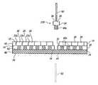
- FIG. 1schematically illustrates one current stacked microelectronic device in which the first and second microelectronic components are wire-bonded to the substrate.
- the stacked microelectronic device 100 of FIG. 1includes a substrate 120 carrying a pair of microelectronic components 130 and 140 .
- the substrate 120which may be a circuit board or the like, has a contact surface 124 bearing a plurality of electrical contacts 126 a - 126 d .
- a first microelectronic component 130is attached to the component surface 124 of the substrate 120 by means of an adhesive 135 .
- the adhesive 135may cover the entire mounting face 132 of the first microelectronic component 130 .
- the active surface 134 of the first microelectronic component 130includes a plurality of electrical contacts 136 a - 136 b .
- a first bonding wire 138 aelectrically connects the first electrical contact 136 a of the first microelectronic component 130 to the first electrical contact 126 a of the substrate 120
- a second bonding wire 138 belectrically connects a second electrical contact 136 b of the first microelectronic component 130 to a second electrical contact 126 b of the substrate 120 .
- the second microelectronic component 140is carried by the first microelectronic component 130 .
- a facing surface 142 of the second microelectronic componentis attached to the active surface 134 of the first microelectronic component 130 via an adhesive layer 145 .
- This adhesive layer 145conventionally has a thickness which is greater than the height to which the bonding wires 138 extend above the active surface 134 so the second microelectronic component 140 does not directly contact or rest against the bonding wires 138 .
- U.S. Pat. No. 5,323,060Fogal et al.
- a first electrical contact 146 a on the outer surface 144 of the second microelectronic component 140can be electrically connected to a third electrical contact 126 c carried by the substrate 120 .
- a second electrical contact 146 b on the outer surface 144can be electrically connected to a fourth electrical contact 126 d carried by the substrate 20 .
- the stacked microelectronic device of FIG. 1includes two microelectronic components 130 and 140 .
- the same approachcan be employed to stack three or more microelectronic components in a single microelectronic device.
- a third microelectronic component(not shown) may be attached to the outer surface 144 of the second microelectronic component 140 using another adhesive layer similar to adhesive layer 145 .
- the third microelectronic componentcan be joined to other electrical contacts carried by the substrate 120 (e.g., contacts 126 e and 126 f ) or one of the other microelectronic components (e.g., contacts 146 ) via wire bonding.
- the system proposed by Fogal et al.provides a relatively simple structure which enables stacking of microelectronic components to increase component density in a microelectronic device.
- a stacked microelectronic devicesuch as that shown in FIG. 1 can present some manufacturing difficulties.
- rapidly and precisely positioning the adhesive layer 145 and the second microelectronic component 140can be a challenge.
- the adhesive layer 145must be positioned within a central area of the first component's active surface 134 inside of the electrical contacts 136 of the first microelectronic component. If the adhesive layer 145 overlaps the electrical contacts 136 , this can damage or interfere with the connection between the electrical contacts 136 and the associated bonding wires 138 .
- microelectronic componentssuch as semiconductor dies
- Many microelectronic componentsare fairly small. It can be difficult to consistently and unerringly position the adhesive layers 145 on previously mounted microelectronic components 130 in a rapid fashion to facilitate mass production of stacked microelectronic devices 100 . After the adhesive layer 145 is applied, the next microelectronic component 140 must be accurately positioned on the adhesive layer 145 . As the number of microelectronic components stacked atop one another in the microelectronic device increases, the chances for error increase concomitantly as one error in alignment or position of any layer of the stacked device can render the entire device unacceptable.
- Embodiments of the present inventionprovide methods of preparing microelectronic components and of manufacturing stacked microelectronic devices. Other embodiments provide microelectronic subassemblies, which subassemblies may be useful in manufacturing stacked microelectronic devices.
- One embodiment of the inventionprovides a method of preparing microelectronic components.
- an adhesive layeris applied on at least a portion of a rear surface of a microelectronic wafer.
- the adhesive layerhas a first surface in contact with the rear surface of the wafer and a second surface oriented away from the wafer.
- a plurality of separable, spaced-apart adhesive padsare defined within the adhesive layer.
- the second surface of the adhesive layeris contacted with a mounting member.
- the waferis diced into a plurality of microelectronic components, with each microelectronic component having a back surface to which at least one of the adhesive pads is attached.
- the adhesive layermay be selectively treated to yield a first adherence between the mounting member and the second surfaces of the adhesive pads and a second, greater adherence between the remainder of the adhesive layer and the mounting member.
- the inventionprovides a method of applying adhesive pads to a plurality of microelectronic components.
- This methodincludes applying an adhesive layer on at least a portion of a rear surface of a microelectronic wafer.
- the microelectronic wafercomprises a plurality of microelectronic components, each of which has a back surface.
- a plurality of separable, spaced-apart adhesive padsare defined within the adhesive layer.
- Each of the microelectronic componentshas an adhesive pad attached to its back surface, with the adhesive pad covering less than the entire back surface of the microelectronic component.
- the microelectronic componentsare singulated. If so desired, the adhesive layer may contact a mounting member prior to singulating the microelectronic components.
- One such subassemblyincludes a microelectronic wafer having an active surface and a rear surface.
- the wafercomprises a plurality of microelectronic components, each of which has a back surface.
- the waferalso includes a plurality of streets defining peripheries of the microelectronic components.
- An adhesive layerhas a first surface in contact with the rear surface of the wafer and covering the back surfaces of the plurality of microelectronic components.
- the adhesive layerincludes an array of separable adhesive pads separated by adhesive boundaries, each adhesive pad being in contact with the back surface of one of the microelectronic components. Each adhesive boundary is aligned with at least one of the streets of the wafer. If so desired, each adhesive pad may cover less than the entire back surface of the microelectronic component to which it is adhered.
- a microelectronic subassembly in accordance with a different embodiment of the inventionincludes a microelectronic wafer comprising a plurality of microelectronic components.
- a mounting memberhas a mounting surface oriented toward a rear face of the wafer.
- An adhesive layerhas a first surface adhered to the rear surface of the wafer and a second surface adhered to the mounting surface of the mounting member.
- the adhesive layerincludes a plurality of adhesive pads separated by adhesive boundaries. Each of the adhesive pads is adhered to one of the microelectronic components.
- the mounting memberis less adherent to the adhesive pads than to the adhesive boundaries.
- FIG. 1is a schematic view of one conventional stacked microelectronic device employing a spacer between the microelectronic components.
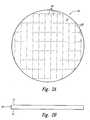
- FIGS. 2A and 2Bare rear and side elevational views, respectively, of a microelectronic wafer.
- FIGS. 3A and 3Bare rear and side elevational views, respectively, of the microelectronic wafer of FIG. 2 bearing an adhesive layer.
- FIGS. 4A and 4Bare rear and side elevational views, respectively, of the wafer and adhesive layer of FIG. 3 bearing a compound mounting member in accordance with one embodiment of the invention.
- FIGS. 5A and 5Bare rear and side elevational views, respectively, of the wafer and adhesive layer of FIG. 3 further including a mounting member and a mask in accordance with another embodiment of the invention.
- FIGS. 6A and 6Bare rear and side elevational views, respectively, of the subassembly of FIG. 5 schematically representing the adhesive layer after treatment through the mask.
- FIG. 7is a side elevational view schematically illustrating a stage in processing a microelectronic component in accordance with a further embodiment of the invention.
- FIG. 2Aillustrates a microelectronic wafer 10 having an active surface 12 and a rear surface 14 .
- the wafer 10may comprise a plurality of microelectronic components 20 .
- the wafer 10may comprise a semiconductor wafer and each of the microelectronic components 20 may comprise a semiconductor die.
- Such semiconductor wafersare commonly manufactured as 200 mm or 300 mm discs with a plurality of semiconductor dies arranged in an array on the disc.
- the microelectronic components 20may be positioned near one another. Commonly, adjacent semiconductor dies are spaced from one another a distance sufficient to accommodate the width of a saw used to cut the wafer 10 into individual microelectronic components 20 .
- microelectronic wafers 10 and their methods of manufactureare well known in the art and need not be detailed here.
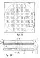
- FIGS. 3 A-Bare rear and side elevational views, respectively, of the wafer 10 of FIG. 2 with an adhesive layer 30 applied on the rear surface 14 of the wafer 10 .
- the adhesive layer 30has a first surface 32 which may be in direct contact with the rear surface 14 of the wafer 10 and a second surface 34 which is oriented away from the wafer 10 .
- the adhesive layer 30desirably covers the back surfaces of at least two adjacent microelectronic components 20 and the street 22 disposed therebetween. In one embodiment, the adhesive layer 30 covers the entire back surface of all of the microelectronic components 20 of the wafer 10 , but need not cover areas of the rear surface 14 of the wafer 10 which do not comprise a back surface of a microelectronic component 20 . In the embodiment shown in FIGS. 3 A-B, the adhesive layer 30 covers the entire rear surface 14 of the wafer 10 .
- the adhesive layer first surface 32may be coextensive with the wafer rear surface 14 .
- the adhesive layer 30comprises a plurality of separable adhesive pads 40 spaced from one another in a predetermined array. Adhesive pads 40 are spaced from one another by boundaries 44 of a predetermined width. The boundaries 44 may be discrete from one another. In the illustrated embodiment, the adhesive boundaries 44 are joined in a continuous structure defining a grid between the adhesive pads 40 .
- the adhesive pads 40should be fairly readily separable from the rest of the adhesive layer 30 . In one embodiment, this is accomplished by forming the adhesive pads 40 of a different material than the remainder of the adhesive layer 30 .
- the adhesive pads 40have peripheries defined by cuts 42 in the adhesive layer. In one embodiment, these cuts extend through substantially the entire thickness of the adhesive layer, extending from the first surface 32 to the second surface 34 of the adhesive layer 30 .
- the cuts 42may be continuous, providing an essentially complete separation between the pads 40 and the adjacent boundaries 44 . In other embodiments, the cuts 42 may extend through less than the entire thickness of the adhesive layer 30 . In still other embodiments, the cuts 42 may be discontinuous, defining the peripheries of the pads 40 as a series of perforations along which the adhesive layer 30 may be readily broken to remove the pads 40 from the remainder of the adhesive layer 30 .
- the array of separable, spaced-apart adhesive pads 40can be defined in any desired fashion.
- the adhesive layer 30is applied to the rear surface 14 of the wafer 10 as a monolithic, continuous layer.
- the adhesive pads 40can be formed in the adhesive layer 30 , such as by cutting the adhesive layer 30 to define the peripheral cuts 42 . This can be accomplished in any known fashion, such as by using lasers or photochemical processes. If the adhesive layer 30 is cut with a wafer saw, the cuts 42 may comprise a series of parallel chords (not shown) which intersect one another to define the peripheries of the adhesive pads 40 . This will also cut the remainder of the adhesive layer 30 into a series of discrete boundaries 44 rather than the continuous, grid-like arrangement shown in FIG. 3A .
- the adhesive pads 40are defined in the adhesive layer 30 before the adhesive layer 30 is applied to the wafer rear surface 14 . This permits mass production of adhesive material having pre-formed adhesive pads 40 defined therein, minimizing the chances of damage to the wafer 10 in the process of forming the cuts 42 after application of the adhesive layer 30 to the wafer 10 . If the cuts 42 are continuous and extend through the entire thickness of the adhesive layer 30 , it may desirable to carry the adhesive layer 30 on a liner (not shown). The liner may be attached to the second surface 34 of the adhesive layer 30 to hold the adhesive pads 40 in place with respect to the remainder of the adhesive layer 30 . If the cuts 42 comprise discontinuous perforations, such a liner may be unnecessary.
- the adhesive pads 40are arranged in an array which is modeled after the arrangement of the microelectronic components 20 on the wafer 10 .
- each adhesive pad 40may be in contact with the back surface of one of the microelectronic components 20 .
- none of the adhesive pads 40are in contact with the back surfaces of more than one microelectronic component 20 .
- the adhesive boundaries 44 between adjacent adhesive pads 40may be generally aligned with the streets 22 of the wafer 10 . In the illustrated embodiment, each of the boundaries 44 is wider than the street 22 with which it is aligned.
- each of the adhesive pads 40has a periphery which is spaced inwardly from the periphery of the microelectronic component 20 to which it is attached. Since the adhesive pads 40 do not cover the entire back surface of the microelectronic components 20 to which they are attached, each microelectronic component 20 has a back surface area which is greater than the contact area between the adhesive pad 40 and the back surface of the microelectronic component 20 .
- the widths of the boundaries 44 and, hence, the distance which the microelectronic component 20 extends outwardly beyond the periphery of the associated adhesive pad 40will vary depending on the particular application.
- the size of the adhesive pad 40is chosen to permit it to be attached to the active surface of another microelectronic component without interfering with the electrical contacts on that active surface.
- the adhesive pad 40may be used instead of the adhesive layer 145 between the two microelectronic components.
- the boundaries of the adhesive pad 40will be selected so that the adhesive pad 40 could be attached to the active surface 134 of the first microelectronic component 130 without covering the electrical contacts 136 .
- the adhesive pads 40may serve as an adhesive layer to connect one of the microelectronic components 20 to another microelectronic component (not shown in FIGS. 3 A-B) in a stacked microelectronic device.
- the material of the adhesive pad 40should be compatible with the microelectronic components 20 of the wafer 10 and the other microelectronic components to which the pads will be attached.
- the adhesive materialshould also be mechanically and chemically stable under the anticipated conditions of use, though some adhesive materials known in the art may require thermal or other curing processes to yield the final desired characteristics.
- the adhesive layer 30(and the adhesive pads 40 defined therein) are formed of a material which is curable by radiation and may also require a secondary thermal cure to yield the final desired adhesive pad 40 .
- the adhesive layer 30can be applied at any suitable thickness.
- the adhesive pads 40may serve as a spacer between microelectronic components in a stacked microelectronic device.
- the thickness of the adhesive pads 40may be selected to ensure adequate clearance between the active surface of the underlying microelectronic component (e.g., surface 134 of the first microelectronic component in FIG. 1 ) and the back surface of the microelectronic component to which it is attached to avoid interference between the microelectronic component 20 and bonding wires (e.g., 138 in FIG. 1 ) attached to the underlying microelectronic component.
- the thicknesswill depend on the loop height of those bonding wires.
- the adhesive layer 30has a thickness of about 6 mils.
- a mounting member 50may be brought into contact with the second surface 34 of the adhesive layer 30 .
- the second surface 34 of the adhesive layer 30is adhered to a mounting surface 52 of the mounting member 50 , effectively connecting the wafer 10 to the mounting member 50 .
- the mounting member 50may comprise a conventional, commercially available dicing tape.
- a wafermay be attached to a dicing tape before the wafer is cut to “singulate” individual microelectronic components.
- Such dicing tapestypically comprise flexible polymeric films.
- the mounting member 50comprises a backing layer 58 which defines the exterior surface 54 of the mounting member 50 and a release layer 56 which defines the mounting surface 52 .
- the release layer 56is selected to control the adherence between the adhesive layer 30 and the mounting member 50 .
- the adherence between the adhesive layer 30 and the release layer 56should be sufficient to enable the wafer 10 to be handled and diced using conventional equipment, but should allow singulated microelectronic components 20 , with the adhesive pad 40 attached thereto, to be lifted away from the mounting member 50 with conventional handling equipment, such as that mentioned below in connection with FIG. 7 .
- the wafer 10may be diced after the adhesive layer 30 is attached to the mounting member 50 .
- the wafer 10may be diced in a conventional fashion, such as by scribing cuts 22 a in the wafer using a conventional wafer saw.
- the cuts 22 amay follow along the path of the streets ( 22 in FIG. 3A ) between adjacent microelectronic components, as is conventional in the art.
- the cuts 22 adesirably pass through substantially the entire thickness of the wafer 10 , but are spaced from the mounting member 50 .
- the cuts 22 aextend through the thickness of the wafer 10 , but do not extend appreciably into the adhesive layer 30 . Because the boundaries 44 between adjacent adhesive pads 40 are aligned with the wafer streets ( 22 in FIG. 3A ), cutting to a depth spaced from the mounting member 50 will leave the boundaries 44 between adjacent adhesive pads 40 largely intact. This facilitates removal of the adhesive pads 40 with the microelectronic components 20 to which they are attached while leaving the remainder of the adhesive layer 30 (including the boundaries 44 ) attached to the mounting member 50 .
- FIGS. 5A-6Billustrate an alternative embodiment of the invention.
- the second surface 34 of the adhesive layer 30is brought into contact with a different mounting member 60 .
- the mounting member 50FIG. 3B
- the mounting member 60FIG. 6B
- the mounting member 60 of FIG. 5Bmay have a relatively high transmissivity of a selected treatment radiation, e.g., ultraviolet (UV) radiation, and is relatively stable under exposure to that radiation.
- UV radiationultraviolet
- a mask 70is positioned between the mounting member 60 and a radiation source 75 .
- the mask 70has a body 72 and a plurality of orifices or windows 74 therethrough. These windows 74 are arranged to align with the either the adhesive pads 40 or the boundaries 44 of the adhesive layer 30 . In the illustrated embodiment, the windows 74 are arranged to align with the adhesive pads 40 and the body 72 of the mask 70 is designed to align with the boundaries 44 between the adhesive pads 40 .
- the windows 74are adapted to transmit radiation from the radiation source 75 while the body 72 limits passage of that radiation. This permits the areas of the adhesive layer 30 aligned with the windows 74 to be selectively exposed to the radiation from the radiation source 75 .
- the material of the adhesive layer 30may be selected to change properties in response to exposure to radiation from the radiation source 75 . This may be done, for example, to alter the properties of the adhesive pads 40 to better bond the adhesive pads to the wafer rear surface 14 or to facilitate defining the adhesive pads 40 or their removal from the remainder of the adhesive layer 30 .
- adhesion between the adhesive layer 30 and the mounting member 60is altered by exposure to radiation from the radiation source 75 .
- the adhesive layer 30may be selectively exposed to yield a first adherence between the mounting member 60 and the second surfaces 34 of the adhesive pads 40 , and a second, greater adherence between the second surface 34 of the remainder of the adhesive layer 30 and the mounting member 60 .
- the adhesive layer 30is a UV- or visible light-curable adhesive material and the radiation source 75 emits radiation of a wavelength adapted to cure the adhesive 30 .
- suitable adhesive materialsare commercially available. These adhesive materials are commonly employed to provide a high level of adhesion between a wafer and a backing tape, for example, during ordinary handling, yet permit ready removal of the backing tape by exposure to an appropriate wavelength of radiation.
- Adhesives expected to be suitable for this purposeinclude ABLELUX “UV/visible curable” or “UV/visible/secondary thermal curable” adhesives, sold by Ablestik Laboratories of Rancho Dominguez, Calif., USA; UV200 and UV500 adhesives available from AI Technology of Princeton Junction, N.J., USA; and D-SERIES adhesives available from Lintec Corporation of Tokyo, Japan.
- FIGS. 6 A-Bschematically illustrate the subassembly of FIGS. 5 A-B after exposure by the radiation source 75 through the mask 70 .
- the adhesive pads in FIGS. 6 A-Bare designated by reference number 40 a and are crosshatched to schematically signify the change induced by exposure to the radiation source 75 .
- FIGS. 6A-6Billustrate the wafer 10 wherein the microelectronic components 20 have been separated by cuts 22 a along the streets ( 22 in FIG. 3A ) of the wafer 10 .
- the cuts 22 a used to dice the wafer 10stop short of cutting through the entire thickness of the adhesive layer 30 .
- the cuts 22 aextend through the thickness of the wafer without cutting into the adhesive layer 30 at all.
- FIG. 7schematically illustrates removal of an individual microelectronic component 20 and its associated adhesive pad 40 a from the diced wafer 10 .
- the active surface 26 of a microelectronic component 20may be contacted with a vacuum tip 90 to sucktorially grasp an individual microelectronic component 20 .
- the adhesive pad 40 a attached to the back surface 24 of the microelectronic component 20will be lifted with the microelectronic component 20 .
- selectively exposing the adhesive pads 40 to the radiation source 75FIG.
- a plunger 92may be urged upwardly against the exterior surface 64 of the mounting member 60 (or exterior surface 54 of the mounting member 50 of FIG. 4B ) to locally deform the mounting member 60 and facilitate selective detachment of the adhesive pad 40 from the mounting member 60 .
- a plunger 92can also be used in connection with embodiments of the invention wherein the adhesive layer 30 is selectively exposed to reduce adherence of the adhesive pads 40 a to the mounting member 60 as suggested in FIG. 7 .
- each of the adhesive pads 40 awill be removed with the microelectronic components 20 to which they are attached. This will leave a remainder of the adhesive layer 30 , including the boundaries 44 which separated the spaced-apart adhesive pads 40 a , attached to the mounting member 60 .
- the vacuum tip 90can remove a single microelectronic component 20 with an attached adhesive pad 40 a .
- This adhesive pad 40may have a periphery spaced inwardly from the periphery of the microelectronic component 20 .
- Thisis an excellent expedient for the manufacture of stacked microelectronic devices.
- current techniquesrequire high-precision placement of a small adhesive layer 145 on the active surface 134 of an individual microelectronic component 130 .
- the process of applying these individual adhesive layers 145can be a manufacturing bottleneck and can increase product losses due to relatively small errors in adhesive layer placement.
- Embodiments of the present inventiongreatly streamline the process of applying and positioning an adhesive which can be used to stack microelectronic components.
- adhesive pads 40can be attached in a batch process to a large number of microelectronic components 20 .
- This subassembly 220can be positioned with respect to another microelectronic component (e.g., 130 in FIG. 1 ) of a stacked microelectronic device.
- the adhesive pad 40can then be used to join the microelectronic component 20 to the underlying microelectronic component and as a spacer to avoid damage to any bonding wires ( 138 in FIG. 1 ) attached to the underlying microelectronic component ( 130 in FIG. 1 ).
Landscapes
- Engineering & Computer Science (AREA)
- Microelectronics & Electronic Packaging (AREA)
- Power Engineering (AREA)
- Computer Hardware Design (AREA)
- Physics & Mathematics (AREA)
- Condensed Matter Physics & Semiconductors (AREA)
- General Physics & Mathematics (AREA)
- Manufacturing & Machinery (AREA)
- Dicing (AREA)
- Adhesive Tapes (AREA)
Abstract
Description
- The present invention relates to methods and apparatus for increasing microelectronic component density. The invention has particular utility in connection with producing vertically superimposed, multi-component microelectronic devices in which at least one of the components is wire-bonded to a substrate.
- Higher performance, lower cost, increased miniaturization of components, and greater packing density of integrated circuits are ongoing goals of the computer industry. Greater integrated circuit density is primarily limited by the space or “real estate” available for mounting microelectronic component on a substrate such as a printed circuit board. The microelectronic component may be electrically connected to circuitry on the circuit board via flip chip attachments, wire bonding, tape automated bonding (TAB), or a variety of other techniques.
- Increasingly, microelectronic components are being vertically stacked atop one another to conserve valuable substrate real estate. In such a vertically stacked assembly, a first microelectronic component is attached directly to the substrate and a second microelectronic component may be physically attached to the first microelectronic component (e.g., stacked on the first microelectronic component). If the first microelectronic component is electrically connected to the substrate via flip chip attachments or TAB, the active surface of the microelectronic component (i.e., the surface bearing the electrical contacts for connection to the circuitry of the microelectronic component) faces toward the substrate. Commonly, the bare backside surface of the first microelectronic component is exposed and faces away from the substrate, and the second microelectronic component is attached directly to the backside surface.
- If the first microelectronic component is electrically connected to the substrate by wire bonding, however, attachment of the second microelectronic component to the first microelectronic component can be more problematic. In wire-bonding techniques, the backside of the first microelectronic component is mounted to the substrate and the active surface of a wire bonded microelectronic component defines the outer surface which faces away from the substrate. The contacts on the active surface are then electrically coupled to the contacts on the substrate by small conductive “bonding” wires that extend from the active surface to the substrate. The wires that electrically connect the active surface of the microelectronic component to the substrate accordingly interfere with attaching the second microelectronic component directly on the active surface.
FIG. 1 schematically illustrates one current stacked microelectronic device in which the first and second microelectronic components are wire-bonded to the substrate. The stackedmicroelectronic device 100 ofFIG. 1 includes asubstrate 120 carrying a pair ofmicroelectronic components substrate 120, which may be a circuit board or the like, has acontact surface 124 bearing a plurality of electrical contacts126a-126d. A firstmicroelectronic component 130 is attached to thecomponent surface 124 of thesubstrate 120 by means of an adhesive135. Theadhesive 135 may cover theentire mounting face 132 of the firstmicroelectronic component 130. Theactive surface 134 of the firstmicroelectronic component 130 includes a plurality of electrical contacts136a-136b. Afirst bonding wire 138aelectrically connects the firstelectrical contact 136aof the firstmicroelectronic component 130 to the firstelectrical contact 126aof thesubstrate 120, and asecond bonding wire 138belectrically connects a secondelectrical contact 136bof the firstmicroelectronic component 130 to a secondelectrical contact 126bof thesubstrate 120.- The second
microelectronic component 140 is carried by the firstmicroelectronic component 130. In some conventional stacked microelectronic devices, a facingsurface 142 of the second microelectronic component is attached to theactive surface 134 of the firstmicroelectronic component 130 via anadhesive layer 145. Thisadhesive layer 145 conventionally has a thickness which is greater than the height to which the bonding wires138 extend above theactive surface 134 so the secondmicroelectronic component 140 does not directly contact or rest against the bonding wires138. Such a structure is shown in U.S. Pat. No. 5,323,060 (Fogal et al.), the entirety of which is incorporated herein by reference. Once the secondmicroelectronic component 140 is in place, a firstelectrical contact 146aon theouter surface 144 of the secondmicroelectronic component 140 can be electrically connected to a thirdelectrical contact 126ccarried by thesubstrate 120. Similarly, a secondelectrical contact 146bon theouter surface 144 can be electrically connected to a fourthelectrical contact 126dcarried by thesubstrate 20. - The stacked microelectronic device of
FIG. 1 includes twomicroelectronic components outer surface 144 of the secondmicroelectronic component 140 using another adhesive layer similar toadhesive layer 145. The third microelectronic component can be joined to other electrical contacts carried by the substrate120 (e.g.,contacts - The system proposed by Fogal et al. provides a relatively simple structure which enables stacking of microelectronic components to increase component density in a microelectronic device. However, a stacked microelectronic device such as that shown in
FIG. 1 can present some manufacturing difficulties. For example, rapidly and precisely positioning theadhesive layer 145 and the secondmicroelectronic component 140 can be a challenge. For this structure to work reliably, theadhesive layer 145 must be positioned within a central area of the first component'sactive surface 134 inside of the electrical contacts136 of the first microelectronic component. If theadhesive layer 145 overlaps the electrical contacts136, this can damage or interfere with the connection between the electrical contacts136 and the associated bonding wires138. Many microelectronic components, such as semiconductor dies, are fairly small. It can be difficult to consistently and unerringly position theadhesive layers 145 on previously mountedmicroelectronic components 130 in a rapid fashion to facilitate mass production of stackedmicroelectronic devices 100. After theadhesive layer 145 is applied, the nextmicroelectronic component 140 must be accurately positioned on theadhesive layer 145. As the number of microelectronic components stacked atop one another in the microelectronic device increases, the chances for error increase concomitantly as one error in alignment or position of any layer of the stacked device can render the entire device unacceptable. - Embodiments of the present invention provide methods of preparing microelectronic components and of manufacturing stacked microelectronic devices. Other embodiments provide microelectronic subassemblies, which subassemblies may be useful in manufacturing stacked microelectronic devices.
- One embodiment of the invention provides a method of preparing microelectronic components. In accordance with this method, an adhesive layer is applied on at least a portion of a rear surface of a microelectronic wafer. The adhesive layer has a first surface in contact with the rear surface of the wafer and a second surface oriented away from the wafer. A plurality of separable, spaced-apart adhesive pads are defined within the adhesive layer. The second surface of the adhesive layer is contacted with a mounting member. The wafer is diced into a plurality of microelectronic components, with each microelectronic component having a back surface to which at least one of the adhesive pads is attached. The microelectronic components and their attached adhesive pads are separated from the mounting member, leaving a remainder of the adhesive layer. In one adaptation of this embodiment, the adhesive layer may be selectively treated to yield a first adherence between the mounting member and the second surfaces of the adhesive pads and a second, greater adherence between the remainder of the adhesive layer and the mounting member.
- In another embodiment, the invention provides a method of applying adhesive pads to a plurality of microelectronic components. This method includes applying an adhesive layer on at least a portion of a rear surface of a microelectronic wafer. The microelectronic wafer comprises a plurality of microelectronic components, each of which has a back surface. A plurality of separable, spaced-apart adhesive pads are defined within the adhesive layer. Each of the microelectronic components has an adhesive pad attached to its back surface, with the adhesive pad covering less than the entire back surface of the microelectronic component. The microelectronic components are singulated. If so desired, the adhesive layer may contact a mounting member prior to singulating the microelectronic components.
- Other embodiments of the invention provide microelectronic subassemblies. One such subassembly includes a microelectronic wafer having an active surface and a rear surface. The wafer comprises a plurality of microelectronic components, each of which has a back surface. The wafer also includes a plurality of streets defining peripheries of the microelectronic components. An adhesive layer has a first surface in contact with the rear surface of the wafer and covering the back surfaces of the plurality of microelectronic components. The adhesive layer includes an array of separable adhesive pads separated by adhesive boundaries, each adhesive pad being in contact with the back surface of one of the microelectronic components. Each adhesive boundary is aligned with at least one of the streets of the wafer. If so desired, each adhesive pad may cover less than the entire back surface of the microelectronic component to which it is adhered.
- A microelectronic subassembly in accordance with a different embodiment of the invention includes a microelectronic wafer comprising a plurality of microelectronic components. A mounting member has a mounting surface oriented toward a rear face of the wafer. An adhesive layer has a first surface adhered to the rear surface of the wafer and a second surface adhered to the mounting surface of the mounting member. The adhesive layer includes a plurality of adhesive pads separated by adhesive boundaries. Each of the adhesive pads is adhered to one of the microelectronic components. The mounting member is less adherent to the adhesive pads than to the adhesive boundaries.
FIG. 1 is a schematic view of one conventional stacked microelectronic device employing a spacer between the microelectronic components.FIGS. 2A and 2B are rear and side elevational views, respectively, of a microelectronic wafer.FIGS. 3A and 3B are rear and side elevational views, respectively, of the microelectronic wafer ofFIG. 2 bearing an adhesive layer.FIGS. 4A and 4B are rear and side elevational views, respectively, of the wafer and adhesive layer ofFIG. 3 bearing a compound mounting member in accordance with one embodiment of the invention.FIGS. 5A and 5B are rear and side elevational views, respectively, of the wafer and adhesive layer ofFIG. 3 further including a mounting member and a mask in accordance with another embodiment of the invention.FIGS. 6A and 6B are rear and side elevational views, respectively, of the subassembly ofFIG. 5 schematically representing the adhesive layer after treatment through the mask.FIG. 7 is a side elevational view schematically illustrating a stage in processing a microelectronic component in accordance with a further embodiment of the invention.- Various embodiments of the present invention provide methods of manufacturing stacked microelectronic devices and subassemblies useful in such manufacture. The following description provides specific details of certain embodiments of the invention illustrated in the drawings to provide a thorough understanding of those embodiments. It should be recognized, however, that the present invention can be reflected in additional embodiments and the invention may be practiced without some of the details in the following description.
FIG. 2A illustrates amicroelectronic wafer 10 having anactive surface 12 and arear surface 14. Thewafer 10 may comprise a plurality ofmicroelectronic components 20. For example, thewafer 10 may comprise a semiconductor wafer and each of themicroelectronic components 20 may comprise a semiconductor die. Such semiconductor wafers are commonly manufactured as 200 mm or 300 mm discs with a plurality of semiconductor dies arranged in an array on the disc. Themicroelectronic components 20 may be positioned near one another. Commonly, adjacent semiconductor dies are spaced from one another a distance sufficient to accommodate the width of a saw used to cut thewafer 10 into individualmicroelectronic components 20. These spaces are commonly aligned with one another to facilitate cutting with a wafer saw, defining so-called “streets”22 between themicroelectronic components 20. Suchmicroelectronic wafers 10 and their methods of manufacture are well known in the art and need not be detailed here.- FIGS.3A-B are rear and side elevational views, respectively, of the
wafer 10 ofFIG. 2 with anadhesive layer 30 applied on therear surface 14 of thewafer 10. Theadhesive layer 30 has afirst surface 32 which may be in direct contact with therear surface 14 of thewafer 10 and asecond surface 34 which is oriented away from thewafer 10. Theadhesive layer 30 desirably covers the back surfaces of at least two adjacentmicroelectronic components 20 and the street22 disposed therebetween. In one embodiment, theadhesive layer 30 covers the entire back surface of all of themicroelectronic components 20 of thewafer 10, but need not cover areas of therear surface 14 of thewafer 10 which do not comprise a back surface of amicroelectronic component 20. In the embodiment shown in FIGS.3A-B, theadhesive layer 30 covers the entirerear surface 14 of thewafer 10. The adhesive layerfirst surface 32 may be coextensive with the waferrear surface 14. - The
adhesive layer 30 comprises a plurality of separableadhesive pads 40 spaced from one another in a predetermined array.Adhesive pads 40 are spaced from one another byboundaries 44 of a predetermined width. Theboundaries 44 may be discrete from one another. In the illustrated embodiment, theadhesive boundaries 44 are joined in a continuous structure defining a grid between theadhesive pads 40. - For reasons explained below, the
adhesive pads 40 should be fairly readily separable from the rest of theadhesive layer 30. In one embodiment, this is accomplished by forming theadhesive pads 40 of a different material than the remainder of theadhesive layer 30. In the illustrated embodiment, theadhesive pads 40 have peripheries defined bycuts 42 in the adhesive layer. In one embodiment, these cuts extend through substantially the entire thickness of the adhesive layer, extending from thefirst surface 32 to thesecond surface 34 of theadhesive layer 30. Thecuts 42 may be continuous, providing an essentially complete separation between thepads 40 and theadjacent boundaries 44. In other embodiments, thecuts 42 may extend through less than the entire thickness of theadhesive layer 30. In still other embodiments, thecuts 42 may be discontinuous, defining the peripheries of thepads 40 as a series of perforations along which theadhesive layer 30 may be readily broken to remove thepads 40 from the remainder of theadhesive layer 30. - The array of separable, spaced-apart
adhesive pads 40 can be defined in any desired fashion. In one embodiment, theadhesive layer 30 is applied to therear surface 14 of thewafer 10 as a monolithic, continuous layer. After theadhesive layer 30 is applied to the waferrear surface 14, theadhesive pads 40 can be formed in theadhesive layer 30, such as by cutting theadhesive layer 30 to define theperipheral cuts 42. This can be accomplished in any known fashion, such as by using lasers or photochemical processes. If theadhesive layer 30 is cut with a wafer saw, thecuts 42 may comprise a series of parallel chords (not shown) which intersect one another to define the peripheries of theadhesive pads 40. This will also cut the remainder of theadhesive layer 30 into a series ofdiscrete boundaries 44 rather than the continuous, grid-like arrangement shown inFIG. 3A . - In an alternative embodiment, the
adhesive pads 40 are defined in theadhesive layer 30 before theadhesive layer 30 is applied to the waferrear surface 14. This permits mass production of adhesive material having pre-formedadhesive pads 40 defined therein, minimizing the chances of damage to thewafer 10 in the process of forming thecuts 42 after application of theadhesive layer 30 to thewafer 10. If thecuts 42 are continuous and extend through the entire thickness of theadhesive layer 30, it may desirable to carry theadhesive layer 30 on a liner (not shown). The liner may be attached to thesecond surface 34 of theadhesive layer 30 to hold theadhesive pads 40 in place with respect to the remainder of theadhesive layer 30. If thecuts 42 comprise discontinuous perforations, such a liner may be unnecessary. - As suggested in
FIG. 3A , theadhesive pads 40 are arranged in an array which is modeled after the arrangement of themicroelectronic components 20 on thewafer 10. In particular, eachadhesive pad 40 may be in contact with the back surface of one of themicroelectronic components 20. In one embodiment, none of theadhesive pads 40 are in contact with the back surfaces of more than onemicroelectronic component 20. Theadhesive boundaries 44 between adjacentadhesive pads 40 may be generally aligned with the streets22 of thewafer 10. In the illustrated embodiment, each of theboundaries 44 is wider than the street22 with which it is aligned. As a consequence, each of theadhesive pads 40 has a periphery which is spaced inwardly from the periphery of themicroelectronic component 20 to which it is attached. Since theadhesive pads 40 do not cover the entire back surface of themicroelectronic components 20 to which they are attached, eachmicroelectronic component 20 has a back surface area which is greater than the contact area between theadhesive pad 40 and the back surface of themicroelectronic component 20. - The widths of the
boundaries 44 and, hence, the distance which themicroelectronic component 20 extends outwardly beyond the periphery of the associatedadhesive pad 40, will vary depending on the particular application. In one embodiment, the size of theadhesive pad 40 is chosen to permit it to be attached to the active surface of another microelectronic component without interfering with the electrical contacts on that active surface. For example, in the context ofFIG. 1 , theadhesive pad 40 may be used instead of theadhesive layer 145 between the two microelectronic components. In this context, the boundaries of theadhesive pad 40 will be selected so that theadhesive pad 40 could be attached to theactive surface 134 of the firstmicroelectronic component 130 without covering the electrical contacts136. - The
adhesive pads 40 may serve as an adhesive layer to connect one of themicroelectronic components 20 to another microelectronic component (not shown in FIGS.3A-B) in a stacked microelectronic device. As such, the material of theadhesive pad 40 should be compatible with themicroelectronic components 20 of thewafer 10 and the other microelectronic components to which the pads will be attached. The adhesive material should also be mechanically and chemically stable under the anticipated conditions of use, though some adhesive materials known in the art may require thermal or other curing processes to yield the final desired characteristics. In one embodiment particularly useful in connection with the process outlined below in connection withFIGS. 5A-7 , for example, the adhesive layer30 (and theadhesive pads 40 defined therein) are formed of a material which is curable by radiation and may also require a secondary thermal cure to yield the final desiredadhesive pad 40. - The
adhesive layer 30 can be applied at any suitable thickness. As noted above and explained more fully below, theadhesive pads 40 may serve as a spacer between microelectronic components in a stacked microelectronic device. The thickness of theadhesive pads 40 may be selected to ensure adequate clearance between the active surface of the underlying microelectronic component (e.g.,surface 134 of the first microelectronic component inFIG. 1 ) and the back surface of the microelectronic component to which it is attached to avoid interference between themicroelectronic component 20 and bonding wires (e.g.,138 inFIG. 1 ) attached to the underlying microelectronic component. The thickness will depend on the loop height of those bonding wires. In one embodiment, theadhesive layer 30 has a thickness of about 6 mils. - As shown in
FIG. 4 , a mountingmember 50 may be brought into contact with thesecond surface 34 of theadhesive layer 30. In one embodiment, thesecond surface 34 of theadhesive layer 30 is adhered to a mountingsurface 52 of the mountingmember 50, effectively connecting thewafer 10 to the mountingmember 50. The mountingmember 50 may comprise a conventional, commercially available dicing tape. In conventional microelectronic component manufacture, a wafer may be attached to a dicing tape before the wafer is cut to “singulate” individual microelectronic components. Such dicing tapes typically comprise flexible polymeric films. - In the embodiment shown in
FIG. 4B , the mountingmember 50 comprises abacking layer 58 which defines theexterior surface 54 of the mountingmember 50 and arelease layer 56 which defines the mountingsurface 52. Therelease layer 56 is selected to control the adherence between theadhesive layer 30 and the mountingmember 50. In particular, the adherence between theadhesive layer 30 and therelease layer 56 should be sufficient to enable thewafer 10 to be handled and diced using conventional equipment, but should allow singulatedmicroelectronic components 20, with theadhesive pad 40 attached thereto, to be lifted away from the mountingmember 50 with conventional handling equipment, such as that mentioned below in connection withFIG. 7 . - As shown in FIGS.4A-B, the
wafer 10 may be diced after theadhesive layer 30 is attached to the mountingmember 50. Thewafer 10 may be diced in a conventional fashion, such as byscribing cuts 22ain the wafer using a conventional wafer saw. Thecuts 22amay follow along the path of the streets (22 inFIG. 3A ) between adjacent microelectronic components, as is conventional in the art. - The
cuts 22adesirably pass through substantially the entire thickness of thewafer 10, but are spaced from the mountingmember 50. In the embodiment shown inFIG. 4B , thecuts 22aextend through the thickness of thewafer 10, but do not extend appreciably into theadhesive layer 30. Because theboundaries 44 between adjacentadhesive pads 40 are aligned with the wafer streets (22 inFIG. 3A ), cutting to a depth spaced from the mountingmember 50 will leave theboundaries 44 between adjacentadhesive pads 40 largely intact. This facilitates removal of theadhesive pads 40 with themicroelectronic components 20 to which they are attached while leaving the remainder of the adhesive layer30 (including the boundaries44) attached to the mountingmember 50. FIGS. 5A-6B illustrate an alternative embodiment of the invention. In accordance with this embodiment, thesecond surface 34 of theadhesive layer 30 is brought into contact with a different mountingmember 60. Whereas the mounting member50 (FIG. 3B ) has a multi-layer structure, the mounting member60 (FIG. 6B ) may have a single monolithic layer which extends from the mountingsurface 62 to theexterior surface 64. The mountingmember 60 ofFIG. 5B may have a relatively high transmissivity of a selected treatment radiation, e.g., ultraviolet (UV) radiation, and is relatively stable under exposure to that radiation.- In accordance with the process outlined in
FIGS. 5A-6B , amask 70 is positioned between the mountingmember 60 and aradiation source 75. Themask 70 has abody 72 and a plurality of orifices orwindows 74 therethrough. Thesewindows 74 are arranged to align with the either theadhesive pads 40 or theboundaries 44 of theadhesive layer 30. In the illustrated embodiment, thewindows 74 are arranged to align with theadhesive pads 40 and thebody 72 of themask 70 is designed to align with theboundaries 44 between theadhesive pads 40. - The
windows 74 are adapted to transmit radiation from theradiation source 75 while thebody 72 limits passage of that radiation. This permits the areas of theadhesive layer 30 aligned with thewindows 74 to be selectively exposed to the radiation from theradiation source 75. - The material of the
adhesive layer 30 may be selected to change properties in response to exposure to radiation from theradiation source 75. This may be done, for example, to alter the properties of theadhesive pads 40 to better bond the adhesive pads to the waferrear surface 14 or to facilitate defining theadhesive pads 40 or their removal from the remainder of theadhesive layer 30. - In one particular embodiment of the invention, adhesion between the
adhesive layer 30 and the mountingmember 60 is altered by exposure to radiation from theradiation source 75. By positioning themask 70 between theradiation source 75 and theadhesive layer 30, theadhesive layer 30 may be selectively exposed to yield a first adherence between the mountingmember 60 and thesecond surfaces 34 of theadhesive pads 40, and a second, greater adherence between thesecond surface 34 of the remainder of theadhesive layer 30 and the mountingmember 60. - In one embodiment, the
adhesive layer 30 is a UV- or visible light-curable adhesive material and theradiation source 75 emits radiation of a wavelength adapted to cure the adhesive30. A variety of suitable adhesive materials are commercially available. These adhesive materials are commonly employed to provide a high level of adhesion between a wafer and a backing tape, for example, during ordinary handling, yet permit ready removal of the backing tape by exposure to an appropriate wavelength of radiation. Adhesives expected to be suitable for this purpose include ABLELUX “UV/visible curable” or “UV/visible/secondary thermal curable” adhesives, sold by Ablestik Laboratories of Rancho Dominguez, Calif., USA; UV200 and UV500 adhesives available from AI Technology of Princeton Junction, N.J., USA; and D-SERIES adhesives available from Lintec Corporation of Tokyo, Japan. - FIGS.6A-B schematically illustrate the subassembly of FIGS.5A-B after exposure by the
radiation source 75 through themask 70. The adhesive pads in FIGS.6A-B are designated byreference number 40aand are crosshatched to schematically signify the change induced by exposure to theradiation source 75. FIGS. 6A-6B illustrate thewafer 10 wherein themicroelectronic components 20 have been separated bycuts 22aalong the streets (22 inFIG. 3A ) of thewafer 10. As with the embodiment ofFIG. 4A , thecuts 22aused to dice thewafer 10 stop short of cutting through the entire thickness of theadhesive layer 30. In the illustrated embodiment, thecuts 22aextend through the thickness of the wafer without cutting into theadhesive layer 30 at all.FIG. 7 schematically illustrates removal of an individualmicroelectronic component 20 and its associatedadhesive pad 40afrom the dicedwafer 10. As is known in the art, theactive surface 26 of amicroelectronic component 20 may be contacted with avacuum tip 90 to sucktorially grasp an individualmicroelectronic component 20. As themicroelectronic component 20 is lifted away from the mountingmember 60, theadhesive pad 40aattached to theback surface 24 of themicroelectronic component 20 will be lifted with themicroelectronic component 20. In the illustrated embodiment, selectively exposing theadhesive pads 40 to the radiation source75 (FIG. 5B ) renders the mountingmember 60 less adherent to theadhesive pads 40athan to theboundaries 44 between theadhesive pads 40a. This facilitates removal of themicroelectronic component 20 with theadhesive pads 40awhile leaving theboundary areas 44 of theadhesive layer 30 attached to the mountingmember 60.- It is not necessary to expose the
adhesive layer 30 to radiation or otherwise treat theadhesive layer 30 to render theadhesive pads 40 relatively less adherent to the mountingmember 60. If amulti-layer mounting member 50 with a release liner56 (FIG. 4B ) is employed, for example, it may be possible to simply lift the dicedmicroelectronic component 20 with the untreatedadhesive pad 40 attached, leaving the rest of theadhesive layer 30 in place. If so desired, aplunger 92 may be urged upwardly against theexterior surface 64 of the mounting member60 (orexterior surface 54 of the mountingmember 50 ofFIG. 4B ) to locally deform the mountingmember 60 and facilitate selective detachment of theadhesive pad 40 from the mountingmember 60. Such aplunger 92 can also be used in connection with embodiments of the invention wherein theadhesive layer 30 is selectively exposed to reduce adherence of theadhesive pads 40ato the mountingmember 60 as suggested inFIG. 7 . - This process may be continued for each of the diced
microelectronic components 20. At the end of process, each of theadhesive pads 40awill be removed with themicroelectronic components 20 to which they are attached. This will leave a remainder of theadhesive layer 30, including theboundaries 44 which separated the spaced-apartadhesive pads 40a, attached to the mountingmember 60. - As shown in
FIG. 7 , thevacuum tip 90 can remove a singlemicroelectronic component 20 with an attachedadhesive pad 40a. Thisadhesive pad 40 may have a periphery spaced inwardly from the periphery of themicroelectronic component 20. This is an excellent expedient for the manufacture of stacked microelectronic devices. As noted above in connection withFIG. 1 , current techniques require high-precision placement of a smalladhesive layer 145 on theactive surface 134 of an individualmicroelectronic component 130. The process of applying these individualadhesive layers 145 can be a manufacturing bottleneck and can increase product losses due to relatively small errors in adhesive layer placement. - Embodiments of the present invention greatly streamline the process of applying and positioning an adhesive which can be used to stack microelectronic components. By applying the
adhesive layer 30 to thewafer 10 before the individualmicroelectronic component 20 are singulated,adhesive pads 40 can be attached in a batch process to a large number ofmicroelectronic components 20. This yields a stackable component subassembly (220 inFIG. 7 ) which includes amicroelectronic component 20 and the attachedadhesive pad 40. Thissubassembly 220 can be positioned with respect to another microelectronic component (e.g.,130 inFIG. 1 ) of a stacked microelectronic device. Theadhesive pad 40 can then be used to join themicroelectronic component 20 to the underlying microelectronic component and as a spacer to avoid damage to any bonding wires (138 inFIG. 1 ) attached to the underlying microelectronic component (130 inFIG. 1 ). - From the foregoing, it will be appreciated that specific embodiments of the invention have been described herein for purposes of illustration, but that various modifications may be made without deviating from the spirit and scope of the invention. Accordingly, the invention is not limited except as by the appended claims.
Claims (21)
Priority Applications (1)
| Application Number | Priority Date | Filing Date | Title |
|---|---|---|---|
| US11/386,208US7297412B2 (en) | 2002-01-16 | 2006-03-22 | Fabrication of stacked microelectronic devices |
Applications Claiming Priority (3)
| Application Number | Priority Date | Filing Date | Title |
|---|---|---|---|
| US10/051,890US6896760B1 (en) | 2002-01-16 | 2002-01-16 | Fabrication of stacked microelectronic devices |
| US10/933,794US7022418B2 (en) | 2002-01-16 | 2004-09-02 | Fabrication of stacked microelectronic devices |
| US11/386,208US7297412B2 (en) | 2002-01-16 | 2006-03-22 | Fabrication of stacked microelectronic devices |
Related Parent Applications (1)
| Application Number | Title | Priority Date | Filing Date |
|---|---|---|---|
| US10/933,794ContinuationUS7022418B2 (en) | 2002-01-16 | 2004-09-02 | Fabrication of stacked microelectronic devices |
Publications (2)
| Publication Number | Publication Date |
|---|---|
| US20060159947A1true US20060159947A1 (en) | 2006-07-20 |
| US7297412B2 US7297412B2 (en) | 2007-11-20 |
Family
ID=34102354
Family Applications (5)
| Application Number | Title | Priority Date | Filing Date |
|---|---|---|---|
| US10/051,890Expired - Fee RelatedUS6896760B1 (en) | 2002-01-16 | 2002-01-16 | Fabrication of stacked microelectronic devices |
| US10/933,770Expired - Fee RelatedUS7037751B2 (en) | 2002-01-16 | 2004-09-02 | Fabrication of stacked microelectronic devices |
| US10/933,794Expired - LifetimeUS7022418B2 (en) | 2002-01-16 | 2004-09-02 | Fabrication of stacked microelectronic devices |
| US11/385,356AbandonedUS20060172510A1 (en) | 2002-01-16 | 2006-03-21 | Fabrication of stacked microelectronic devices |
| US11/386,208Expired - LifetimeUS7297412B2 (en) | 2002-01-16 | 2006-03-22 | Fabrication of stacked microelectronic devices |
Family Applications Before (4)
| Application Number | Title | Priority Date | Filing Date |
|---|---|---|---|
| US10/051,890Expired - Fee RelatedUS6896760B1 (en) | 2002-01-16 | 2002-01-16 | Fabrication of stacked microelectronic devices |
| US10/933,770Expired - Fee RelatedUS7037751B2 (en) | 2002-01-16 | 2004-09-02 | Fabrication of stacked microelectronic devices |
| US10/933,794Expired - LifetimeUS7022418B2 (en) | 2002-01-16 | 2004-09-02 | Fabrication of stacked microelectronic devices |
| US11/385,356AbandonedUS20060172510A1 (en) | 2002-01-16 | 2006-03-21 | Fabrication of stacked microelectronic devices |
Country Status (1)
| Country | Link |
|---|---|
| US (5) | US6896760B1 (en) |
Cited By (4)
| Publication number | Priority date | Publication date | Assignee | Title |
|---|---|---|---|---|
| US20070036932A1 (en)* | 2005-07-19 | 2007-02-15 | Micron Technology, Inc. | Methods for releasably attaching support members to microfeature workpieces and microfeature assemblies formed using such methods |
| US20070045803A1 (en)* | 2005-08-26 | 2007-03-01 | Micron Technology, Inc. | Microelectronic device packages, stacked microelectronic device packages, and methods for manufacturing microelectronic devices |
| US20070241078A1 (en)* | 2006-03-14 | 2007-10-18 | Micron Technology, Inc. | Methods for releasably attaching support members to microfeature workpieces |
| US20090239337A1 (en)* | 2005-08-19 | 2009-09-24 | Micron Technology, Inc. | Microelectronic devices, stacked microelectronic devices, and methods for manufacturing microelectronic devices |
Families Citing this family (23)
| Publication number | Priority date | Publication date | Assignee | Title |
|---|---|---|---|---|
| US6896760B1 (en)* | 2002-01-16 | 2005-05-24 | Micron Technology, Inc. | Fabrication of stacked microelectronic devices |
| US20040102022A1 (en)* | 2002-11-22 | 2004-05-27 | Tongbi Jiang | Methods of fabricating integrated circuitry |
| JP2004273895A (en)* | 2003-03-11 | 2004-09-30 | Disco Abrasive Syst Ltd | Method of dividing semiconductor wafer |
| TWI233170B (en)* | 2004-02-05 | 2005-05-21 | United Microelectronics Corp | Ultra-thin wafer level stack packaging method and structure using thereof |
| WO2005093829A1 (en)* | 2004-03-16 | 2005-10-06 | Infineon Technologies Ag | Semiconductor package having an interfacial adhesive layer |
| JP4830740B2 (en)* | 2005-11-16 | 2011-12-07 | 株式会社デンソー | Manufacturing method of semiconductor chip |
| JP4777830B2 (en)* | 2006-06-06 | 2011-09-21 | 株式会社ディスコ | Wafer division method |
| US7846776B2 (en)* | 2006-08-17 | 2010-12-07 | Micron Technology, Inc. | Methods for releasably attaching sacrificial support members to microfeature workpieces and microfeature devices formed using such methods |
| US7858493B2 (en)* | 2007-02-23 | 2010-12-28 | Finisar Corporation | Cleaving edge-emitting lasers from a wafer cell |
| US7825517B2 (en)* | 2007-07-16 | 2010-11-02 | Taiwan Semiconductor Manufacturing Company, Ltd. | Method for packaging semiconductor dies having through-silicon vias |
| US7829379B2 (en)* | 2007-10-17 | 2010-11-09 | Analog Devices, Inc. | Wafer level stacked die packaging |
| KR101469770B1 (en)* | 2007-11-21 | 2014-12-09 | 페어차일드코리아반도체 주식회사 | Power device package and manufacturing method thereof |
| US20100054289A1 (en)* | 2008-08-29 | 2010-03-04 | Cobolt Ab | Solid-state laser |
| US9142434B2 (en)* | 2008-10-23 | 2015-09-22 | Freescale Semiconductor, Inc. | Method for singulating electronic components from a substrate |
| FR2956244A1 (en)* | 2010-02-05 | 2011-08-12 | St Microelectronics Crolles 2 | Electronic device, has intermediate layer provided next to cutting areas defined between chips, where intermediate layer comprises primary and secondary regions made of materials having different mechanical characteristics values |
| JP2012069747A (en)* | 2010-09-24 | 2012-04-05 | Teramikros Inc | Semiconductor device and method of manufacturing the same |
| JP2012109538A (en) | 2010-10-29 | 2012-06-07 | Tokyo Ohka Kogyo Co Ltd | Laminate and method for separating the same |
| JP5802106B2 (en)* | 2010-11-15 | 2015-10-28 | 東京応化工業株式会社 | Laminate and separation method |
| US20120175746A1 (en)* | 2011-01-12 | 2012-07-12 | Kim Younsang | Selective Deposition in the Fabrication of Electronic Substrates |
| US9764532B2 (en) | 2014-07-01 | 2017-09-19 | Isola Usa Corp. | Prepregs including UV curable resins useful for manufacturing semi-flexible PCBs |
| JP5908543B2 (en)* | 2014-08-07 | 2016-04-26 | 日東電工株式会社 | Manufacturing method of semiconductor device |
| GB2544335A (en)* | 2015-11-13 | 2017-05-17 | Oculus Vr Llc | A method and apparatus for use in the manufacture of a display element |
| CN111599753B (en)* | 2020-05-29 | 2023-10-13 | 绍兴同芯成集成电路有限公司 | Thin wafer cooling fin and manufacturing process thereof |
Citations (51)
| Publication number | Priority date | Publication date | Assignee | Title |
|---|---|---|---|---|
| US5098501A (en)* | 1989-12-08 | 1992-03-24 | Sumitomo Electric Industries, Ltd. | Pickup method and the pickup apparatus for chip-type part |
| US5128831A (en)* | 1991-10-31 | 1992-07-07 | Micron Technology, Inc. | High-density electronic package comprising stacked sub-modules which are electrically interconnected by solder-filled vias |
| US5252857A (en)* | 1991-08-05 | 1993-10-12 | International Business Machines Corporation | Stacked DCA memory chips |
| US5323060A (en)* | 1993-06-02 | 1994-06-21 | Micron Semiconductor, Inc. | Multichip module having a stacked chip arrangement |
| US5397634A (en)* | 1993-07-22 | 1995-03-14 | Rexham Graphics Incorporated | Transferable protective cover layers |
| US5422435A (en)* | 1992-05-22 | 1995-06-06 | National Semiconductor Corporation | Stacked multi-chip modules and method of manufacturing |
| US5518957A (en)* | 1991-10-10 | 1996-05-21 | Samsung Electronics Co., Ltd. | Method for making a thin profile semiconductor package |
| US5827394A (en)* | 1996-07-15 | 1998-10-27 | Vanguard International Semiconductor Corporation | Step and repeat exposure method for loosening integrated circuit dice from a radiation sensitive adhesive tape backing |
| US5883426A (en)* | 1996-04-18 | 1999-03-16 | Nec Corporation | Stack module |
| US5926951A (en)* | 1993-11-16 | 1999-07-27 | Formfactor, Inc. | Method of stacking electronic components |
| US5946553A (en)* | 1991-06-04 | 1999-08-31 | Micron Technology, Inc. | Process for manufacturing a semiconductor package with bi-substrate die |
| US5952725A (en)* | 1996-02-20 | 1999-09-14 | Micron Technology, Inc. | Stacked semiconductor devices |
| US5986209A (en)* | 1997-07-09 | 1999-11-16 | Micron Technology, Inc. | Package stack via bottom leaded plastic (BLP) packaging |
| US5990566A (en)* | 1998-05-20 | 1999-11-23 | Micron Technology, Inc. | High density semiconductor package |
| USRE36469E (en)* | 1988-09-30 | 1999-12-28 | Micron Technology, Inc. | Packaging for semiconductor logic devices |
| US6020629A (en)* | 1998-06-05 | 2000-02-01 | Micron Technology, Inc. | Stacked semiconductor package and method of fabrication |
| US6028365A (en)* | 1998-03-30 | 2000-02-22 | Micron Technology, Inc. | Integrated circuit package and method of fabrication |
| USRE36613E (en)* | 1993-04-06 | 2000-03-14 | Micron Technology, Inc. | Multi-chip stacked devices |
| US6051878A (en)* | 1997-03-10 | 2000-04-18 | Micron Technology, Inc. | Method of constructing stacked packages |
| US6072233A (en)* | 1998-05-04 | 2000-06-06 | Micron Technology, Inc. | Stackable ball grid array package |
| US6072236A (en)* | 1996-03-07 | 2000-06-06 | Micron Technology, Inc. | Micromachined chip scale package |
| US6084308A (en)* | 1998-06-30 | 2000-07-04 | National Semiconductor Corporation | Chip-on-chip integrated circuit package and method for making the same |
| US6153924A (en)* | 1998-02-23 | 2000-11-28 | Micron Technology, Inc. | Multilayered lead frame for semiconductor package |
| US6160718A (en)* | 1998-12-08 | 2000-12-12 | Viking Components | Multi-chip package with stacked chips and interconnect bumps |
| US6175149B1 (en)* | 1998-02-13 | 2001-01-16 | Micron Technology, Inc. | Mounting multiple semiconductor dies in a package |
| US6176966B1 (en)* | 1997-06-12 | 2001-01-23 | Lintec Corporation | Method of die bonding electronic component and die bonding apparatus thereof |
| US6212767B1 (en)* | 1999-08-31 | 2001-04-10 | Micron Technology, Inc. | Assembling a stacked die package |
| US6225194B1 (en)* | 1996-12-19 | 2001-05-01 | Lintec Corporation | Process for producing chip and pressure sensitive adhesive sheet for said process |
| US6225689B1 (en)* | 1998-08-21 | 2001-05-01 | Micron Technology, Inc. | Low profile multi-IC chip package connector |
| US6228548B1 (en)* | 1998-02-27 | 2001-05-08 | Micron Technology, Inc. | Method of making a multichip semiconductor package |
| US6235554B1 (en)* | 1995-11-27 | 2001-05-22 | Micron Technology, Inc. | Method for fabricating stackable chip scale semiconductor package |
| US6262895B1 (en)* | 2000-01-13 | 2001-07-17 | John A. Forthun | Stackable chip package with flex carrier |
| US6261865B1 (en)* | 1998-10-06 | 2001-07-17 | Micron Technology, Inc. | Multi chip semiconductor package and method of construction |
| US6281577B1 (en)* | 1996-06-28 | 2001-08-28 | Pac Tech-Packaging Technologies Gmbh | Chips arranged in plurality of planes and electrically connected to one another |
| US6294839B1 (en)* | 1999-08-30 | 2001-09-25 | Micron Technology, Inc. | Apparatus and methods of packaging and testing die |
| US6297547B1 (en)* | 1998-02-13 | 2001-10-02 | Micron Technology Inc. | Mounting multiple semiconductor dies in a package |
| US6303981B1 (en)* | 1999-09-01 | 2001-10-16 | Micron Technology, Inc. | Semiconductor package having stacked dice and leadframes and method of fabrication |
| US6344976B1 (en)* | 1997-04-07 | 2002-02-05 | Micron Technology, Inc. | Interdigitated leads-over-chip lead frame device and method for supporting an integrated circuit die |
| US6351028B1 (en)* | 1999-02-08 | 2002-02-26 | Micron Technology, Inc. | Multiple die stack apparatus employing T-shaped interposer elements |
| US20020055238A1 (en)* | 2000-08-31 | 2002-05-09 | Lintec Corporation | Process for producing semiconductor device |
| US6514795B1 (en)* | 2001-10-10 | 2003-02-04 | Micron Technology, Inc. | Packaged stacked semiconductor die and method of preparing same |
| US20030042615A1 (en)* | 2001-08-30 | 2003-03-06 | Tongbi Jiang | Stacked microelectronic devices and methods of fabricating same |
| US6552910B1 (en)* | 2000-06-28 | 2003-04-22 | Micron Technology, Inc. | Stacked-die assemblies with a plurality of microelectronic devices and methods of manufacture |
| US6560117B2 (en)* | 2000-06-28 | 2003-05-06 | Micron Technology, Inc. | Packaged microelectronic die assemblies and methods of manufacture |
| US6589809B1 (en)* | 2001-07-16 | 2003-07-08 | Micron Technology, Inc. | Method for attaching semiconductor components to a substrate using local UV curing of dicing tape |
| US20030162325A1 (en)* | 2002-01-09 | 2003-08-28 | Micron Technology, Inc. | Stacked die in die BGA package |
| US6620649B2 (en)* | 2001-04-24 | 2003-09-16 | Oki Electric Industry Co., Ltd. | Method for selectively providing adhesive on a semiconductor device |
| US20030178715A1 (en)* | 2002-03-20 | 2003-09-25 | Bae Systems | Method for stacking chips within a multichip module package |
| US6706557B2 (en)* | 2001-09-21 | 2004-03-16 | Micron Technology, Inc. | Method of fabricating stacked die configurations utilizing redistribution bond pads |
| US6825572B2 (en)* | 2001-12-08 | 2004-11-30 | Micron Technology, Inc. | Die package |
| US20050026415A1 (en)* | 2002-01-16 | 2005-02-03 | Micron Technology, Inc. | Fabrication of stacked microelectronic devices |
Family Cites Families (2)
| Publication number | Priority date | Publication date | Assignee | Title |
|---|---|---|---|---|
| US6064308A (en) | 1996-10-25 | 2000-05-16 | Pole/Zero Corporation | RF signaling system and system for controlling the whereabouts of animals using same |
| US6221767B1 (en)* | 1999-10-28 | 2001-04-24 | United Microelectronics Corp. | Method of fabricating a silicide landing pad |
- 2002
- 2002-01-16USUS10/051,890patent/US6896760B1/ennot_activeExpired - Fee Related
- 2004
- 2004-09-02USUS10/933,770patent/US7037751B2/ennot_activeExpired - Fee Related
- 2004-09-02USUS10/933,794patent/US7022418B2/ennot_activeExpired - Lifetime
- 2006
- 2006-03-21USUS11/385,356patent/US20060172510A1/ennot_activeAbandoned
- 2006-03-22USUS11/386,208patent/US7297412B2/ennot_activeExpired - Lifetime
Patent Citations (58)
| Publication number | Priority date | Publication date | Assignee | Title |
|---|---|---|---|---|
| USRE36469E (en)* | 1988-09-30 | 1999-12-28 | Micron Technology, Inc. | Packaging for semiconductor logic devices |
| US5098501A (en)* | 1989-12-08 | 1992-03-24 | Sumitomo Electric Industries, Ltd. | Pickup method and the pickup apparatus for chip-type part |
| US6020624A (en)* | 1991-06-04 | 2000-02-01 | Micron Technology, Inc. | Semiconductor package with bi-substrate die |
| US5946553A (en)* | 1991-06-04 | 1999-08-31 | Micron Technology, Inc. | Process for manufacturing a semiconductor package with bi-substrate die |
| US5252857A (en)* | 1991-08-05 | 1993-10-12 | International Business Machines Corporation | Stacked DCA memory chips |
| US5518957A (en)* | 1991-10-10 | 1996-05-21 | Samsung Electronics Co., Ltd. | Method for making a thin profile semiconductor package |
| US5128831A (en)* | 1991-10-31 | 1992-07-07 | Micron Technology, Inc. | High-density electronic package comprising stacked sub-modules which are electrically interconnected by solder-filled vias |
| US5422435A (en)* | 1992-05-22 | 1995-06-06 | National Semiconductor Corporation | Stacked multi-chip modules and method of manufacturing |
| USRE36613E (en)* | 1993-04-06 | 2000-03-14 | Micron Technology, Inc. | Multi-chip stacked devices |
| US5323060A (en)* | 1993-06-02 | 1994-06-21 | Micron Semiconductor, Inc. | Multichip module having a stacked chip arrangement |
| US5397634A (en)* | 1993-07-22 | 1995-03-14 | Rexham Graphics Incorporated | Transferable protective cover layers |
| US5926951A (en)* | 1993-11-16 | 1999-07-27 | Formfactor, Inc. | Method of stacking electronic components |
| US6235554B1 (en)* | 1995-11-27 | 2001-05-22 | Micron Technology, Inc. | Method for fabricating stackable chip scale semiconductor package |
| US5952725A (en)* | 1996-02-20 | 1999-09-14 | Micron Technology, Inc. | Stacked semiconductor devices |
| US6072236A (en)* | 1996-03-07 | 2000-06-06 | Micron Technology, Inc. | Micromachined chip scale package |
| US5883426A (en)* | 1996-04-18 | 1999-03-16 | Nec Corporation | Stack module |
| US6281577B1 (en)* | 1996-06-28 | 2001-08-28 | Pac Tech-Packaging Technologies Gmbh | Chips arranged in plurality of planes and electrically connected to one another |
| US5827394A (en)* | 1996-07-15 | 1998-10-27 | Vanguard International Semiconductor Corporation | Step and repeat exposure method for loosening integrated circuit dice from a radiation sensitive adhesive tape backing |
| US6225194B1 (en)* | 1996-12-19 | 2001-05-01 | Lintec Corporation | Process for producing chip and pressure sensitive adhesive sheet for said process |
| US6051878A (en)* | 1997-03-10 | 2000-04-18 | Micron Technology, Inc. | Method of constructing stacked packages |
| US6344976B1 (en)* | 1997-04-07 | 2002-02-05 | Micron Technology, Inc. | Interdigitated leads-over-chip lead frame device and method for supporting an integrated circuit die |
| US6176966B1 (en)* | 1997-06-12 | 2001-01-23 | Lintec Corporation | Method of die bonding electronic component and die bonding apparatus thereof |
| US5986209A (en)* | 1997-07-09 | 1999-11-16 | Micron Technology, Inc. | Package stack via bottom leaded plastic (BLP) packaging |
| US6175149B1 (en)* | 1998-02-13 | 2001-01-16 | Micron Technology, Inc. | Mounting multiple semiconductor dies in a package |
| US6297547B1 (en)* | 1998-02-13 | 2001-10-02 | Micron Technology Inc. | Mounting multiple semiconductor dies in a package |
| US6153924A (en)* | 1998-02-23 | 2000-11-28 | Micron Technology, Inc. | Multilayered lead frame for semiconductor package |
| US6228548B1 (en)* | 1998-02-27 | 2001-05-08 | Micron Technology, Inc. | Method of making a multichip semiconductor package |
| US6028365A (en)* | 1998-03-30 | 2000-02-22 | Micron Technology, Inc. | Integrated circuit package and method of fabrication |
| US6072233A (en)* | 1998-05-04 | 2000-06-06 | Micron Technology, Inc. | Stackable ball grid array package |
| US5990566A (en)* | 1998-05-20 | 1999-11-23 | Micron Technology, Inc. | High density semiconductor package |
| US6020629A (en)* | 1998-06-05 | 2000-02-01 | Micron Technology, Inc. | Stacked semiconductor package and method of fabrication |
| US6084308A (en)* | 1998-06-30 | 2000-07-04 | National Semiconductor Corporation | Chip-on-chip integrated circuit package and method for making the same |
| US6225689B1 (en)* | 1998-08-21 | 2001-05-01 | Micron Technology, Inc. | Low profile multi-IC chip package connector |
| US6258623B1 (en)* | 1998-08-21 | 2001-07-10 | Micron Technology, Inc. | Low profile multi-IC chip package connector |
| US6261865B1 (en)* | 1998-10-06 | 2001-07-17 | Micron Technology, Inc. | Multi chip semiconductor package and method of construction |
| US6160718A (en)* | 1998-12-08 | 2000-12-12 | Viking Components | Multi-chip package with stacked chips and interconnect bumps |
| US6351028B1 (en)* | 1999-02-08 | 2002-02-26 | Micron Technology, Inc. | Multiple die stack apparatus employing T-shaped interposer elements |
| US6294839B1 (en)* | 1999-08-30 | 2001-09-25 | Micron Technology, Inc. | Apparatus and methods of packaging and testing die |
| US6212767B1 (en)* | 1999-08-31 | 2001-04-10 | Micron Technology, Inc. | Assembling a stacked die package |
| US6303981B1 (en)* | 1999-09-01 | 2001-10-16 | Micron Technology, Inc. | Semiconductor package having stacked dice and leadframes and method of fabrication |
| US6262895B1 (en)* | 2000-01-13 | 2001-07-17 | John A. Forthun | Stackable chip package with flex carrier |
| US6560117B2 (en)* | 2000-06-28 | 2003-05-06 | Micron Technology, Inc. | Packaged microelectronic die assemblies and methods of manufacture |
| US6552910B1 (en)* | 2000-06-28 | 2003-04-22 | Micron Technology, Inc. | Stacked-die assemblies with a plurality of microelectronic devices and methods of manufacture |
| US20020055238A1 (en)* | 2000-08-31 | 2002-05-09 | Lintec Corporation | Process for producing semiconductor device |
| US6558975B2 (en)* | 2000-08-31 | 2003-05-06 | Lintec Corporation | Process for producing semiconductor device |
| US6620649B2 (en)* | 2001-04-24 | 2003-09-16 | Oki Electric Industry Co., Ltd. | Method for selectively providing adhesive on a semiconductor device |
| US6589809B1 (en)* | 2001-07-16 | 2003-07-08 | Micron Technology, Inc. | Method for attaching semiconductor components to a substrate using local UV curing of dicing tape |
| US20030042615A1 (en)* | 2001-08-30 | 2003-03-06 | Tongbi Jiang | Stacked microelectronic devices and methods of fabricating same |
| US6706557B2 (en)* | 2001-09-21 | 2004-03-16 | Micron Technology, Inc. | Method of fabricating stacked die configurations utilizing redistribution bond pads |
| US6514795B1 (en)* | 2001-10-10 | 2003-02-04 | Micron Technology, Inc. | Packaged stacked semiconductor die and method of preparing same |
| US6825572B2 (en)* | 2001-12-08 | 2004-11-30 | Micron Technology, Inc. | Die package |
| US20030162325A1 (en)* | 2002-01-09 | 2003-08-28 | Micron Technology, Inc. | Stacked die in die BGA package |
| US20050026395A1 (en)* | 2002-01-16 | 2005-02-03 | Micron Technology, Inc. | Fabrication of stacked microelectronic devices |
| US20050026415A1 (en)* | 2002-01-16 | 2005-02-03 | Micron Technology, Inc. | Fabrication of stacked microelectronic devices |
| US6896760B1 (en)* | 2002-01-16 | 2005-05-24 | Micron Technology, Inc. | Fabrication of stacked microelectronic devices |
| US7022418B2 (en)* | 2002-01-16 | 2006-04-04 | Micron Technology, Inc. | Fabrication of stacked microelectronic devices |
| US7037751B2 (en)* | 2002-01-16 | 2006-05-02 | Micron Technology, Inc. | Fabrication of stacked microelectronic devices |
| US20030178715A1 (en)* | 2002-03-20 | 2003-09-25 | Bae Systems | Method for stacking chips within a multichip module package |
Cited By (22)
| Publication number | Priority date | Publication date | Assignee | Title |
|---|---|---|---|---|
| US20070036932A1 (en)* | 2005-07-19 | 2007-02-15 | Micron Technology, Inc. | Methods for releasably attaching support members to microfeature workpieces and microfeature assemblies formed using such methods |
| US7833601B2 (en) | 2005-07-19 | 2010-11-16 | Micron Technology, Inc. | Methods for releasably attaching support members to microfeature workpieces and microfeature assemblies formed using such methods |
| US8507318B2 (en) | 2005-08-19 | 2013-08-13 | Micron Technology, Inc. | Method for manufacturing microelectronic devices |
| US11239128B2 (en) | 2005-08-19 | 2022-02-01 | Micron Technology, Inc. | Microelectronic devices, stacked microelectronic devices, and methods for manufacturing microelectronic devices |
| US10431513B2 (en) | 2005-08-19 | 2019-10-01 | Micron Technology, Inc. | Microelectronic devices, stacked microelectronic devices, and methods for manufacturing microelectronic devices |
| US9640458B2 (en) | 2005-08-19 | 2017-05-02 | Micron Technology, Inc. | Stacked microelectronic devices |
| US20090239337A1 (en)* | 2005-08-19 | 2009-09-24 | Micron Technology, Inc. | Microelectronic devices, stacked microelectronic devices, and methods for manufacturing microelectronic devices |
| US8823159B2 (en) | 2005-08-19 | 2014-09-02 | Micron Technology, Inc. | Stacked microelectronic devices |
| US9583476B2 (en) | 2005-08-26 | 2017-02-28 | Micron Technology, Inc. | Microelectronic device packages, stacked microelectronic device packages, and methods for manufacturing microelectronic devices |
| US7504284B2 (en) | 2005-08-26 | 2009-03-17 | Micron Technology, Inc. | Microelectronic device packages, stacked microelectronic device packages, and methods for manufacturing microelectronic devices |
| US8030748B2 (en) | 2005-08-26 | 2011-10-04 | Micron Technology, Inc. | Microelectronic device packages, stacked microelectronic device packages, and methods for manufacturing microelectronic devices |
| US8519523B2 (en) | 2005-08-26 | 2013-08-27 | Micron Technology, Inc. | Microelectronic device packages, stacked microelectronic device packages, and methods for manufacturing microelectronic devices |
| US20070045803A1 (en)* | 2005-08-26 | 2007-03-01 | Micron Technology, Inc. | Microelectronic device packages, stacked microelectronic device packages, and methods for manufacturing microelectronic devices |
| US10861824B2 (en) | 2005-08-26 | 2020-12-08 | Micron Technology, Inc. | Microelectronic device packages, stacked microelectronic device packages, and methods for manufacturing microelectronic devices |
| US9299684B2 (en) | 2005-08-26 | 2016-03-29 | Micron Technology, Inc. | Microelectronic device packages, stacked microelectronic device packages, and methods for manufacturing microelectronic devices |
| US10153254B2 (en) | 2005-08-26 | 2018-12-11 | Micron Technology, Inc. | Microelectronic device packages, stacked microelectronic device packages, and methods for manufacturing microelectronic devices |
| US20100247875A1 (en)* | 2006-03-14 | 2010-09-30 | Micron Technology, Inc. | Methods and systems for releasably attaching support members to microfeature workpieces |
| US9595504B2 (en) | 2006-03-14 | 2017-03-14 | Micron Technology, Inc. | Methods and systems for releasably attaching support members to microfeature workpieces |
| US7749349B2 (en) | 2006-03-14 | 2010-07-06 | Micron Technology, Inc. | Methods and systems for releasably attaching support members to microfeature workpieces |
| US20070241078A1 (en)* | 2006-03-14 | 2007-10-18 | Micron Technology, Inc. | Methods for releasably attaching support members to microfeature workpieces |
| US8999498B2 (en) | 2006-03-14 | 2015-04-07 | Micron Technology, Inc. | Methods and systems for releasably attaching support members to microfeature workpieces |
| US8361604B2 (en) | 2006-03-14 | 2013-01-29 | Micron Technology, Inc. | Methods and systems for releasably attaching support members to microfeature workpieces |
Also Published As
| Publication number | Publication date |
|---|---|
| US7297412B2 (en) | 2007-11-20 |
| US6896760B1 (en) | 2005-05-24 |
| US20060172510A1 (en) | 2006-08-03 |
| US20050026395A1 (en) | 2005-02-03 |
| US7022418B2 (en) | 2006-04-04 |
| US7037751B2 (en) | 2006-05-02 |
| US20050026415A1 (en) | 2005-02-03 |
Similar Documents
| Publication | Publication Date | Title |
|---|---|---|
| US7297412B2 (en) | Fabrication of stacked microelectronic devices | |
| US7285864B2 (en) | Stack MCP | |
| US7294531B2 (en) | Wafer level chip stack method | |
| TWI284960B (en) | Manufacturing method of semiconductor device | |
| CN1327500C (en) | Dicing tape ateaching unit and sequenced system having same | |
| KR100517075B1 (en) | Method for manufacturing semiconductor device | |
| JP4409014B2 (en) | Manufacturing method of semiconductor device | |
| US6759745B2 (en) | Semiconductor device and manufacturing method thereof | |
| US20020037631A1 (en) | Method for manufacturing semiconductor devices | |
| US6777310B2 (en) | Method of fabricating semiconductor devices on a semiconductor wafer using a carrier plate during grinding and dicing steps | |
| JP2002075921A (en) | Manufacturing method of semiconductor device | |
| US9362105B2 (en) | Pre-cut wafer applied underfill film on dicing tape | |
| JP2000182995A (en) | Manufacture of semiconductor device | |
| TWI384522B (en) | Semiconductor spacer structure, method for bonding a semiconductor spacer die to a support surface, and method for combining a multi-wafer semiconductor package | |
| US4883773A (en) | Method of producing magnetosensitive semiconductor devices | |
| JP2001060591A (en) | Manufacture of semiconductor device | |
| JPH1174230A (en) | Method for manufacturing thin film semiconductor device | |
| JP2001085453A (en) | Method of manufacturing semiconductor device | |
| JP2001156028A (en) | Method of manufacturing semiconductor device | |
| JPH04336448A (en) | Fabrication of semiconductor device | |
| JP2004047903A (en) | Semiconductor device and its manufacture | |
| JP4043720B2 (en) | Semiconductor device and manufacturing method of semiconductor device | |
| JP2003037030A (en) | Semiconductor device | |
| KR20050038502A (en) | Manufacturing method for stack ship package | |
| TW200411882A (en) | Flip-chip bump manufacturing method of semiconductor chip |
Legal Events
| Date | Code | Title | Description |
|---|---|---|---|
| FEPP | Fee payment procedure | Free format text:PAYOR NUMBER ASSIGNED (ORIGINAL EVENT CODE: ASPN); ENTITY STATUS OF PATENT OWNER: LARGE ENTITY | |
| STCF | Information on status: patent grant | Free format text:PATENTED CASE | |
| FPAY | Fee payment | Year of fee payment:4 | |
| FPAY | Fee payment | Year of fee payment:8 | |
| AS | Assignment | Owner name:U.S. BANK NATIONAL ASSOCIATION, AS COLLATERAL AGENT, CALIFORNIA Free format text:SECURITY INTEREST;ASSIGNOR:MICRON TECHNOLOGY, INC.;REEL/FRAME:038669/0001 Effective date:20160426 Owner name:U.S. BANK NATIONAL ASSOCIATION, AS COLLATERAL AGEN Free format text:SECURITY INTEREST;ASSIGNOR:MICRON TECHNOLOGY, INC.;REEL/FRAME:038669/0001 Effective date:20160426 | |
| AS | Assignment | Owner name:MORGAN STANLEY SENIOR FUNDING, INC., AS COLLATERAL AGENT, MARYLAND Free format text:PATENT SECURITY AGREEMENT;ASSIGNOR:MICRON TECHNOLOGY, INC.;REEL/FRAME:038954/0001 Effective date:20160426 Owner name:MORGAN STANLEY SENIOR FUNDING, INC., AS COLLATERAL Free format text:PATENT SECURITY AGREEMENT;ASSIGNOR:MICRON TECHNOLOGY, INC.;REEL/FRAME:038954/0001 Effective date:20160426 | |
| AS | Assignment | Owner name:U.S. BANK NATIONAL ASSOCIATION, AS COLLATERAL AGENT, CALIFORNIA Free format text:CORRECTIVE ASSIGNMENT TO CORRECT THE REPLACE ERRONEOUSLY FILED PATENT #7358718 WITH THE CORRECT PATENT #7358178 PREVIOUSLY RECORDED ON REEL 038669 FRAME 0001. ASSIGNOR(S) HEREBY CONFIRMS THE SECURITY INTEREST;ASSIGNOR:MICRON TECHNOLOGY, INC.;REEL/FRAME:043079/0001 Effective date:20160426 Owner name:U.S. BANK NATIONAL ASSOCIATION, AS COLLATERAL AGEN Free format text:CORRECTIVE ASSIGNMENT TO CORRECT THE REPLACE ERRONEOUSLY FILED PATENT #7358718 WITH THE CORRECT PATENT #7358178 PREVIOUSLY RECORDED ON REEL 038669 FRAME 0001. ASSIGNOR(S) HEREBY CONFIRMS THE SECURITY INTEREST;ASSIGNOR:MICRON TECHNOLOGY, INC.;REEL/FRAME:043079/0001 Effective date:20160426 | |
| AS | Assignment | Owner name:JPMORGAN CHASE BANK, N.A., AS COLLATERAL AGENT, ILLINOIS Free format text:SECURITY INTEREST;ASSIGNORS:MICRON TECHNOLOGY, INC.;MICRON SEMICONDUCTOR PRODUCTS, INC.;REEL/FRAME:047540/0001 Effective date:20180703 Owner name:JPMORGAN CHASE BANK, N.A., AS COLLATERAL AGENT, IL Free format text:SECURITY INTEREST;ASSIGNORS:MICRON TECHNOLOGY, INC.;MICRON SEMICONDUCTOR PRODUCTS, INC.;REEL/FRAME:047540/0001 Effective date:20180703 | |
| AS | Assignment | Owner name:MICRON TECHNOLOGY, INC., IDAHO Free format text:RELEASE BY SECURED PARTY;ASSIGNOR:U.S. BANK NATIONAL ASSOCIATION, AS COLLATERAL AGENT;REEL/FRAME:047243/0001 Effective date:20180629 | |
| MAFP | Maintenance fee payment | Free format text:PAYMENT OF MAINTENANCE FEE, 12TH YEAR, LARGE ENTITY (ORIGINAL EVENT CODE: M1553); ENTITY STATUS OF PATENT OWNER: LARGE ENTITY Year of fee payment:12 | |
| AS | Assignment | Owner name:MICRON TECHNOLOGY, INC., IDAHO Free format text:RELEASE BY SECURED PARTY;ASSIGNOR:MORGAN STANLEY SENIOR FUNDING, INC., AS COLLATERAL AGENT;REEL/FRAME:050937/0001 Effective date:20190731 | |
| AS | Assignment | Owner name:MICRON SEMICONDUCTOR PRODUCTS, INC., IDAHO Free format text:RELEASE BY SECURED PARTY;ASSIGNOR:JPMORGAN CHASE BANK, N.A., AS COLLATERAL AGENT;REEL/FRAME:051028/0001 Effective date:20190731 Owner name:MICRON TECHNOLOGY, INC., IDAHO Free format text:RELEASE BY SECURED PARTY;ASSIGNOR:JPMORGAN CHASE BANK, N.A., AS COLLATERAL AGENT;REEL/FRAME:051028/0001 Effective date:20190731 |