US20060158270A1 - Electronic circuit including at least one first and one second differential pair with the transistors sharing one and the same well - Google Patents
Electronic circuit including at least one first and one second differential pair with the transistors sharing one and the same wellDownload PDFInfo
- Publication number
- US20060158270A1 US20060158270A1US11/311,931US31193105AUS2006158270A1US 20060158270 A1US20060158270 A1US 20060158270A1US 31193105 AUS31193105 AUS 31193105AUS 2006158270 A1US2006158270 A1US 2006158270A1
- Authority
- US
- United States
- Prior art keywords
- transistors
- differential
- vco
- pairs
- topology
- Prior art date
- Legal status (The legal status is an assumption and is not a legal conclusion. Google has not performed a legal analysis and makes no representation as to the accuracy of the status listed.)
- Granted
Links
- 238000005516engineering processMethods0.000claimsdescription11
- 230000003071parasitic effectEffects0.000description16
- 238000010586diagramMethods0.000description13
- 238000009792diffusion processMethods0.000description7
- 239000002184metalSubstances0.000description7
- 238000004519manufacturing processMethods0.000description6
- 239000004065semiconductorSubstances0.000description6
- 230000010355oscillationEffects0.000description4
- 230000000737periodic effectEffects0.000description3
- 238000000034methodMethods0.000description2
- 239000000758substrateSubstances0.000description2
- 239000003990capacitorSubstances0.000description1
- 230000009977dual effectEffects0.000description1
Images


Classifications
- H—ELECTRICITY
- H03—ELECTRONIC CIRCUITRY
- H03F—AMPLIFIERS
- H03F3/00—Amplifiers with only discharge tubes or only semiconductor devices as amplifying elements
- H03F3/45—Differential amplifiers
- H03F3/45071—Differential amplifiers with semiconductor devices only
- H03F3/45076—Differential amplifiers with semiconductor devices only characterised by the way of implementation of the active amplifying circuit in the differential amplifier
- H03F3/45475—Differential amplifiers with semiconductor devices only characterised by the way of implementation of the active amplifying circuit in the differential amplifier using IC blocks as the active amplifying circuit
- H—ELECTRICITY
- H03—ELECTRONIC CIRCUITRY
- H03F—AMPLIFIERS
- H03F3/00—Amplifiers with only discharge tubes or only semiconductor devices as amplifying elements
- H03F3/45—Differential amplifiers
- H03F3/45071—Differential amplifiers with semiconductor devices only
- H03F3/45076—Differential amplifiers with semiconductor devices only characterised by the way of implementation of the active amplifying circuit in the differential amplifier
- H03F3/45179—Differential amplifiers with semiconductor devices only characterised by the way of implementation of the active amplifying circuit in the differential amplifier using MOSFET transistors as the active amplifying circuit
- H—ELECTRICITY
- H10—SEMICONDUCTOR DEVICES; ELECTRIC SOLID-STATE DEVICES NOT OTHERWISE PROVIDED FOR
- H10D—INORGANIC ELECTRIC SEMICONDUCTOR DEVICES
- H10D89/00—Aspects of integrated devices not covered by groups H10D84/00 - H10D88/00
- H10D89/10—Integrated device layouts
Definitions
- the field of the disclosureis that of electronic integrated circuits and more particularly that of integrated circuit design.
- the disclosurerelates to the optimisation of the topology of integrated circuits, and particularly the optimisation of the topology of voltage-controlled oscillators (VCO).
- VCOvoltage-controlled oscillators
- the function of a voltage-controlled oscillatoris to generate a periodic output signal, the frequency of which is a function of a continuous voltage applied to an input. It thus allows periodic signals to be generated, the frequency of which is open to selection.
- VCOvoltage-controlled oscillator
- a second example of a VCOis the voltage-controlled differential oscillator, designated hereinafter as a differential VCO.
- the differential VCOconventionally includes four transistor based differential pairs.
- FIG. 1shows a simplified diagram of a conventional differential VCO 10 .
- the differential VCOincludes first 11 , second 12 , third 13 and fourth 14 amplifying stages.
- Amplifying stages 11 to 14are polarised by means of a bias voltage VBIAS applied to an input 15 of the differential VCO 10 .
- Each stageincludes two inputs, 111 and 112 , 121 and 122 , 131 and 132 , 141 and 142 respectively, and an output 133 , 123 , 133 and 143 respectively.
- the output 133 of the third stagesupplies the periodic output voltage of the differential VCO 10 the frequency of which depends on the bias voltage VBIAS.
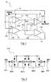
- FIG. 2Ashows the diagram of a conventional amplifying stage of the differential VCO 10 , for example the first stage 11 .
- all the stages 11 to 14 of the differential VCO 10are identical.
- This first stage 11conventionally includes:
- the inputs 111 , 112 of the first stage 11are connected to the gates of the transistors M 1 , M 2 of the differential pair 114 .
- the output 113 of the first stage 11is connected to the drain of the transistor M 2 of the differential pair 114 .
- the sources of the transistors M 1 , M 2 of the differential pair 114are connected to one and the same common node N.
- a known technique for increasing the power supply rejection of an amplifying stage 21is to connect the NWELL wells of the transistors 201 , 202 of the differential pair 214 to a common node N.
- each of the transistors of the pairfor example the transistor M 1
- FIG. 3shows the diagram of a differential pair 314 in which each of the transistors has been split so as to form two pairs of transistors M 11 and M 12 , M 22 and M 21 respectively.
- FIG. 4is a diagram of the topology of the transistors M 11 , M 12 , M 22 and M 21 of the differential pair 314 in FIG. 3 in the case of a “crossed pair” arrangement. A number of metal strips (not shown in FIG. 4 ) allow the electrical connections in FIG. 3 to be made between the different contacts of the transistors.
- the areas marked by black dotsare doped zones in which the transistors are made.
- the 4 transistors of the differential pair 314are equivalent to two transistors forming the pair 314 .
- the “crossed pair” arrangementmakes it possible to ensure a good uniformity of dimensions of these two equivalent transistors when the pair is manufactured.
- a lack of uniformity in respect of the dimensions of the transistors of a differential pair(for example the pair 314 in FIG. 3 ) generates an offset voltage between the two inputs of the pair ( 311 and 312 ) that may well interfere with the operation of an amplifying stage that includes the pair.
- a first drawback of this conventional arrangementis that it generates parasitic capacitances (capacitances due to the metal strips connecting the transistors, diffusion capacitance of the transistors, bottom or sidewall capacitance between the wells of the transistors and the substrate, etc) that restrict the performance of the differential VCO, in particular by reducing its oscillation frequency.
- VCOsare able to operate in different frequency ranges and to be made according to different technologies, each associated with a pitch that is generally indicated in microns.
- VCOsfor example in order to make a phase locked loop (or PLL) for a USB port according to the USB 2.0 standard, it may be necessary to make VCOs by means of technologies that have a pitch below 0.5 ⁇ m and which operate at a frequency of about 480 MHz (for an internal clock of 12 MHz).
- differential VCOsare unable to operate at significant frequencies (above 300 MHz, in very small-scale technologies, in other words below 0.5 ⁇ m).
- An embodiment of the present inventionis directed to an electronic circuit that includes at least one first and one second differential pair, each including a plurality of transistors. All the transistors of said first and second differential pairs are included in a single well.
- a general principle of an embodiment of the inventionis based on the implementation of a plurality of differential pairs brought close together so that their transistors share one and the same well.
- An embodiment of the inventionis equally applicable to circuits based on differential pairs arranged as “crossed pairs” as it is to circuits based on differential pairs that are not arranged as crossed pairs.
- the electronic circuitincludes four amplifying stages each including a differential pair, all the transistors of said differential pairs being included in a single well.
- At least one of said differential pairsmay include first and second transistors, which are P-type MOS transistors, and said first and second transistors may share one and the same single drain.
- At least one of said differential pairsmay include third and fourth transistors, which are N-type MOS transistors, and said first and second transistors may share one and the same single source.
- an embodiment of the inventioncounters the prejudices of the person skilled in the art by proposing an electronic circuit based on differential pairs with the transistors of the differential pairs not being arranged as a “crossed pair” and therefore able not to be of uniform dimensions.
- a double transistoris implemented, being obtained by means of two transistors that share one and the same drain or one and the same source.
- the electronic circuitis manufactured by means of a technology with a pitch below 0.5 ⁇ m.
- the electronic circuitis a voltage-controlled differential oscillator.
- the electronic circuitis designed to operate at a frequency above 300 MHz.
- one or more embodiments of the inventionpropose a differential VCO operating at frequencies above 300 MHz and made by means of a technology below 0.5 ⁇ m.
- FIG. 1shows a simplified diagram of a conventional differential VCO based on four amplifying stages
- FIGS. 2A and 2Bshow two diagrams of a conventional amplifying stage based on a differential pair of the differential VCO in FIG. 1 ;
- FIG. 3shows the diagram of a conventional differential pair made from four transistors
- FIG. 4is a diagram of the topology of the transistors of the differential pair in FIG. 3 in the case of a “crossed pair” arrangement;
- FIG. 5is a diagram of the topology of the transistors of a conventional differential VCO including four differential pairs arranged as “crossed pairs”;
- FIG. 6is a diagram of the topology of the transistors of a differential VCO according to a first embodiment of the invention.
- FIG. 7is a diagram of the topology of the transistors of a differential VCO according to a second embodiment of the invention.
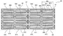
- the topology of a conventional differential VCO 50is shown, in relation to FIG. 5 , with the transistors arranged as “crossed pairs”.
- This VCO 50includes sixteen P-type MOS transistors 501 to 516 , forming first 501 , 505 , 509 , 513 , second 502 , 506 , 510 , 514 , third 503 , 507 , 511 , 515 and fourth 504 , 508 , 512 , 516 transistors of four differential pairs 51 to 54 (the other components of the VCO 50 are not shown in this FIG. 5 ).
- the four transistors of each of the differential pairs 51 to 54are manufactured in one and the same well, 571 , 572 , 573 , 574 respectively.
- the first transistor 501 of the differential pair 51 of the VCO 50has a source 5011 , a drain 5012 and a gate 5013 .
- the four differential pairs 51 to 54occupy a significant semiconductor surface.
- a total surface occupied by the four differential pairsis obtained that is substantially equal to 280 ⁇ m.
- a conventional transistor arrangement of this kind for implementing a differential VCOrequires the employment of a high number of metal strips in order to establish the electrical connections of the contacts of the transistors needed for the VCO to operate.
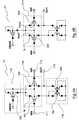
- a diagramis shown in relation to FIG. 6 of the topology of the transistors of a differential VCO 60 according to a first embodiment of the invention in which the transistors are arranged as “crossed pairs”.
- the VCO 60also includes sixteen P-type MOS transistors 601 to 616 , forming first 601 , 605 , 609 , 613 , second 602 , 606 , 610 , 614 , third 603 , 607 , 611 , 615 and fourth 604 , 608 , 612 , 616 transistors of four differential pairs 61 to 64 (the other components of the VCO 60 are not shown in this FIG. 6 ).
- the first transistor 601 of the differential pair 61 of the VCO 60has a source 6011 , a drain 6012 , and a gate 6013 .
- the four differential pairs 61 to 64are manufactured in one and the same and single well 67 .
- this topologymakes it possible to substantially reduce the semiconductor surface occupied by the differential pairs compared with the topology of the conventional differential VCO 50 in FIG. 5 .
- transistors 601 to 616that have a gate width (denoted w 6 ) identical to that of the transistors 501 to 516 of the conventional VCO 50 (in other words substantially equal to 5 ⁇ m)
- a total surface occupied by the four differential pairs 61 to 64is obtained that is substantially equal to 240 ⁇ m.
- this topology according to the first embodiment of the inventionmakes it possible to reduce the parasitic capacitances related to the electrical strips compared with the topology of the conventional differential VCO 50 . Indeed, it makes it possible to reduce the length (given the fact that the differential pairs 61 to 64 have been brought closer together) of the metal strips needed to establish the electrical connections of the differential VCO 60 , and therefore the parasitic capacitances related to these electrical strips.
- This topology according to the first embodiment of the inventionadditionally makes it possible to reduce the parasitic capacitances between the well and the substrate of the transistors 601 to 616 .
- the bottom capacitancecan be distinguished from the sidewall capacitance.
- the bottom CSURF2 and sidewall CPERI2 capacitancesmay be written:
- the topology according to the first embodiment of the inventionmakes it possible to reduce by 50% the parasitic sidewall capacitance compared with the topology of the conventional differential VCO in FIG. 5 .
- a diagramis presented in relation to FIG. 7 of the topology of the transistors of a differential VCO 70 according to a second embodiment of the invention, in which the transistors are not arranged as “crossed pairs”.
- This VCO 70includes eight P-type MOS transistors 711 , 721 , 731 , 741 , 712 , 722 , 732 , 742 , forming first 711 , 721 , 731 , 741 and second 712 , 722 , 732 , 742 transistors of four differential pairs 71 to 74 (the other components of the VCO 70 are not shown in this FIG. 7 ).
- the first 711 and second 712 transistors of the differential pair 71 of the VCO 70each have a source 715 , 716 respectively and a gate 717 , 718 respectively.
- the four differential pairs 71 to 74are manufactured in one and the same and single well 76 .
- the first 711 , 721 , 731 , 741 and second 712 , 722 , 732 , 742 transistorsshare one and the same single drain 714 , 724 , 734 , 744 respectively.
- the four differential pairs 71 to 74 of the topology in FIG. 7occupy a semiconductor surface that is smaller than the four differential pairs arranged according to the topology as “crossed pairs” of the first embodiment of the invention in FIG. 6 (and a fortiori even smaller than the four differential pairs arranged according to the conventional topology in FIG. 5 ).
- each differential pair 71 to 74in order to share a common drain 714 , 724 , 734 , 744 , the first and second transistors are brought closer together in a horizontal direction 75 compared with the “crossed pairs” topology of the first embodiment of the invention in FIG. 6 .
- each of the transistors of each of the differential pairsis equivalent to two transistors of a differential .pair, for example the first and third transistors 601 , 603 of the pair 61 , of the VCO 60 according to the first embodiment of the invention in FIG. 6 .
- first 711 , 721 , 731 , 741 and second 712 , 722 , 732 , 742 transistorsthat have a gate width substantially equal to 10 ⁇ m
- a total surface occupied by the four differential pairsis obtained that is substantially equal to 185 ⁇ m
- this topologymakes it possible to reduce the number (given the common drains and reduced number of transistors) and the length (given the fact that the transistors have been brought closer together) of the metal strips needed to establish the electrical connections of the differential VCO 70 , and therefore the parasitic capacitances related to these electrical strips.
- these connectionshave no cause to be there, which gives freedom from sixteen intersecting parasitic capacitances of 1.5 fF each compared with the “crossed pairs” topology.
- this topology according to the second embodiment of the inventionmakes it possible to reduce the influence of the parasitic diffusion capacitances of the transistors of the differential VCO 70 compared with the parasitic diffusion capacitances of the transistors of the
- ais the source length of the transistors 501 and 503
- bis the source width of the transistors 501 and 503
- Cjais the junction capacitance per unit area (expressed as F/m 2 )
- Cjbis the sidewall capacitance per unit length (expressed as F/m).
- the diffusion capacitance CdiffDC2 seen by a sourcemay be written:
- the topology according to the second embodiment of the inventionmakes it possible to reduce the diffusion capacitance by 10% compared with the “crossed pairs” topology.
- transistors of the differential VCO in FIG. 7are not arranged as “crossed pairs” and that they are of small dimensions (for example, of the order of 2 ⁇ m for the length of the source and drain diffusion zones and 0.47 ⁇ m for their width), these transistors are not generally of uniform dimensions.
- differential VCOsuse the noise of their power supply for their start-up (the noise is broadband and therefore includes a component that has the right frequency, which is amplified and which initiates the oscillation).
- each amplifying stage of the differential VCO 10 in FIG. 1reacts like a comparator, it is the voltage difference applied to its two differential inputs that allows an output voltage to be generated.
- the four amplifying stages 11 to 14generate instability in the operation of the VCO 10 and therefore an oscillation.
- each of the inputs of the differential amplifiersmay be at the same potential despite the presence of the power supply noise, which corresponds to a VCO rest point and therefore an absence of oscillation.
- the offsets between the inputs of each of the pairs 61 to 64allow freedom from this rest point.
- the first and second transistorsshare one and the same source and not one and the same drain.
- one or more embodiments of the inventionovercome drawbacks of the prior art.
- One aspect of an embodiment of the inventionprovides a differential VCO operating at high frequency and made in a very small-scale technology.
- Another aspect of an embodiment of the inventionimplements a VCO of this kind that is high-performance and that in particular offers a reduction in parasitic capacitances compared with conventional VCOs.
- Another aspect of an embodiment of the inventionprovides a VCO of this kind that requires a reduced number of stages during its manufacture and that occupies a small amount of semiconductor surface.
- Yet another aspect of an embodiment of the inventionimplements a VCO of this kind that is straightforward and inexpensive to manufacture.
- one or more embodiments of the inventionalso apply to any electronic circuit that includes at least two differential pairs.
Landscapes
- Engineering & Computer Science (AREA)
- Power Engineering (AREA)
- Amplifiers (AREA)
Abstract
Description
- The field of the disclosure is that of electronic integrated circuits and more particularly that of integrated circuit design.
- To be more precise, the disclosure relates to the optimisation of the topology of integrated circuits, and particularly the optimisation of the topology of voltage-controlled oscillators (VCO).
- The function of a voltage-controlled oscillator is to generate a periodic output signal, the frequency of which is a function of a continuous voltage applied to an input. It thus allows periodic signals to be generated, the frequency of which is open to selection.
- There are several types of voltage-controlled oscillator. A first example of a VCO is the VCO of the RC type, which is based on loading and unloading a capacitance through a capacitor.
- A second example of a VCO is the voltage-controlled differential oscillator, designated hereinafter as a differential VCO. The differential VCO conventionally includes four transistor based differential pairs.
FIG. 1 shows a simplified diagram of a conventionaldifferential VCO 10. The differential VCO includes first11, second12, third13 and fourth14 amplifying stages. Amplifyingstages 11 to14 are polarised by means of a bias voltage VBIAS applied to aninput 15 of thedifferential VCO 10. Each stage includes two inputs,111 and112,121 and122,131 and132,141 and142 respectively, and anoutput - The
output 133 of the third stage supplies the periodic output voltage of thedifferential VCO 10 the frequency of which depends on the bias voltage VBIAS. FIG. 2A shows the diagram of a conventional amplifying stage of thedifferential VCO 10, for example thefirst stage 11. For example, all thestages 11 to14 of thedifferential VCO 10 are identical.- This
first stage 11 conventionally includes: - a conventional
differential pair 114 based on two P-type MOS transistors M1, M2; - a
current source 115 including one P-type MOS transistor M3; and - an
active load 116 based on two N-type MOS transistors M4, M5.
- a conventional
- The
inputs first stage 11 are connected to the gates of the transistors M1, M2 of thedifferential pair 114. Theoutput 113 of thefirst stage 11 is connected to the drain of the transistor M2 of thedifferential pair 114. - The sources of the transistors M1, M2 of the
differential pair 114 are connected to one and the same common node N. - A known technique (shown in
FIG. 2B ) for increasing the power supply rejection of anamplifying stage 21 is to connect the NWELL wells of thetransistors differential pair 214 to a common node N. - When designing a differential pair that includes two transistors M1 and M2, each of the transistors of the pair, for example the transistor M1, can conventionally be replaced by two transistors M11, M12 each having a gate width two times smaller and a gate length identical to that of the transistor M1.
FIG. 3 shows the diagram of adifferential pair 314 in which each of the transistors has been split so as to form two pairs of transistors M11 and M12, M22 and M21 respectively.FIG. 4 is a diagram of the topology of the transistors M11, M12, M22 and M21 of thedifferential pair 314 inFIG. 3 in the case of a “crossed pair” arrangement. A number of metal strips (not shown inFIG. 4 ) allow the electrical connections inFIG. 3 to be made between the different contacts of the transistors.- It may be noted that in this
FIG. 4 but also in those that follow, the areas marked by black dots are doped zones in which the transistors are made. - The 4 transistors of the
differential pair 314 are equivalent to two transistors forming thepair 314. The “crossed pair” arrangement makes it possible to ensure a good uniformity of dimensions of these two equivalent transistors when the pair is manufactured. - Indeed, any variation in dimension due to the manufacturing process, and any interference that causes parasitic effects in the transistors (noise, temperature variation, etc) is transmitted in the same way to each of these two equivalent transistors.
- In fact, a lack of uniformity in respect of the dimensions of the transistors of a differential pair (for example the
pair 314 inFIG. 3 ) generates an offset voltage between the two inputs of the pair (311 and312) that may well interfere with the operation of an amplifying stage that includes the pair. - Specialists in the manufacture of transistors therefore consider that it is necessary to employ the “crossed pairs” arrangement when manufacturing a differential pair.
- Conventionally, in a differential pair arranged as a “crossed pair”, the man skilled in the art combines the four transistors in one and the same well41 (in
FIG. 4 ). In this way, when a VCO is made based on conventional differential pairs of this kind, each of the pairs is included in a different well. - Unfortunately, a first drawback of this conventional arrangement is that it generates parasitic capacitances (capacitances due to the metal strips connecting the transistors, diffusion capacitance of the transistors, bottom or sidewall capacitance between the wells of the transistors and the substrate, etc) that restrict the performance of the differential VCO, in particular by reducing its oscillation frequency.
- VCOs are able to operate in different frequency ranges and to be made according to different technologies, each associated with a pitch that is generally indicated in microns.
- The growing need to reduce power consumption and the dimensions of electronic systems based on integrated circuits has led designers of VCOs of this kind to use manufacturing technologies that have an increasingly small pitch.
- In this way, for example in order to make a phase locked loop (or PLL) for a USB port according to the USB 2.0 standard, it may be necessary to make VCOs by means of technologies that have a pitch below 0.5 μm and which operate at a frequency of about 480 MHz (for an internal clock of 12 MHz).
- One drawback of differential VCOs is, according to the man skilled in the art, that they are unable to operate at significant frequencies (above 300 MHz, in very small-scale technologies, in other words below 0.5 μm).
- Indeed, the person skilled in the art considers that, should it be required to make a differential VCO operating at these frequencies from a technology below 0.5 μm, the transistors of the differential pairs of this differential VCO would be too small to ensure good uniformity in the dimensions of the transistors of the VCO despite the use of the “crossed pairs” arrangement. It is for this reason, generally speaking, that VCOs operating at high frequencies (above 300 MHz) and made from very small-scale technologies (below 0.5 μm) are VCOs of the RC type.
- An embodiment of the present invention is directed to an electronic circuit that includes at least one first and one second differential pair, each including a plurality of transistors. All the transistors of said first and second differential pairs are included in a single well.
- A general principle of an embodiment of the invention is based on the implementation of a plurality of differential pairs brought close together so that their transistors share one and the same well.
- An embodiment of the invention is equally applicable to circuits based on differential pairs arranged as “crossed pairs” as it is to circuits based on differential pairs that are not arranged as crossed pairs.
- In this way, combining the transistors of the differential pairs in a single well makes it possible to obtain circuits based on differential pairs that have parasitic capacitances, particularly bottom and sidewall capacitances, and an occupied semiconductor surface that are clearly smaller compared with conventional circuits.
- In one or more embodiments of the invention, the electronic circuit includes four amplifying stages each including a differential pair, all the transistors of said differential pairs being included in a single well.
- At least one of said differential pairs may include first and second transistors, which are P-type MOS transistors, and said first and second transistors may share one and the same single drain.
- At least one of said differential pairs may include third and fourth transistors, which are N-type MOS transistors, and said first and second transistors may share one and the same single source.
- In this way, an embodiment of the invention counters the prejudices of the person skilled in the art by proposing an electronic circuit based on differential pairs with the transistors of the differential pairs not being arranged as a “crossed pair” and therefore able not to be of uniform dimensions.
- For at least one differential pair, for example, a double transistor is implemented, being obtained by means of two transistors that share one and the same drain or one and the same source.
- Implementing a double transistor of this kind can make it possible to further reduce the parasitic capacitances and the occupied semiconductor surface in the circuit.
- According to an embodiment of the invention, the electronic circuit is manufactured by means of a technology with a pitch below 0.5 μm.
- According to an embodiment of the invention, the electronic circuit is a voltage-controlled differential oscillator.
- For example, the electronic circuit is designed to operate at a frequency above 300 MHz.
- In this way, one or more embodiments of the invention propose a differential VCO operating at frequencies above 300 MHz and made by means of a technology below 0.5 μm.
- Other characteristics of one or more embodiments of the invention will emerge more clearly from reading the following description of two embodiments, given by way of simple illustrative and non-restrictive examples and of the appended drawings.
FIG. 1 shows a simplified diagram of a conventional differential VCO based on four amplifying stages;FIGS. 2A and 2B show two diagrams of a conventional amplifying stage based on a differential pair of the differential VCO inFIG. 1 ;FIG. 3 shows the diagram of a conventional differential pair made from four transistors;FIG. 4 is a diagram of the topology of the transistors of the differential pair inFIG. 3 in the case of a “crossed pair” arrangement;FIG. 5 is a diagram of the topology of the transistors of a conventional differential VCO including four differential pairs arranged as “crossed pairs”;FIG. 6 is a diagram of the topology of the transistors of a differential VCO according to a first embodiment of the invention;FIG. 7 is a diagram of the topology of the transistors of a differential VCO according to a second embodiment of the invention.- The topology of a conventional
differential VCO 50 is shown, in relation toFIG. 5 , with the transistors arranged as “crossed pairs”. - This
VCO 50 includes sixteen P-type MOS transistors 501 to516, forming first501,505,509,513, second502,506,510,514, third503,507,511,515 and fourth504,508,512,516 transistors of fourdifferential pairs 51 to54 (the other components of theVCO 50 are not shown in thisFIG. 5 ). - The four transistors of each of the differential pairs51 to54 are manufactured in one and the same well,571,572,573,574 respectively.
- For example, the
first transistor 501 of thedifferential pair 51 of theVCO 50 has a source5011, a drain5012 and a gate5013. - The four
differential pairs 51 to54 occupy a significant semiconductor surface. For example, fortransistors 501 to516 that have a gate width (denoted w5) substantially equal to 4 μm, a total surface occupied by the four differential pairs is obtained that is substantially equal to 280 μm. - A conventional transistor arrangement of this kind for implementing a differential VCO requires the employment of a high number of metal strips in order to establish the electrical connections of the contacts of the transistors needed for the VCO to operate.
- In this way, a topology of this kind generates, through the high number of metal strips required, significant parasitic capacitances.
- We will consider hereinafter the implementation of differential VCOs through the use of technologies with a pitch below 0.5 μm, and which operate at frequencies above 300 MHz.
- A diagram is shown in relation to
FIG. 6 of the topology of the transistors of adifferential VCO 60 according to a first embodiment of the invention in which the transistors are arranged as “crossed pairs”. - The
VCO 60 also includes sixteen P-type MOS transistors 601 to616, forming first601,605,609,613, second602,606,610,614, third603,607,611,615 and fourth604,608,612,616 transistors of fourdifferential pairs 61 to64 (the other components of theVCO 60 are not shown in thisFIG. 6 ). - For example, the
first transistor 601 of thedifferential pair 61 of theVCO 60 has asource 6011, adrain 6012, and agate 6013. - Unlike the topology of the conventional differential VCO50 (
FIG. 5 ), in the topology according to this first embodiment of the invention, the fourdifferential pairs 61 to64 are manufactured in one and the same andsingle well 67. - In this way, this topology according to the first embodiment of the invention makes it possible to substantially reduce the semiconductor surface occupied by the differential pairs compared with the topology of the conventional
differential VCO 50 inFIG. 5 . For example, fortransistors 601 to616 that have a gate width (denoted w6) identical to that of thetransistors 501 to516 of the conventional VCO50 (in other words substantially equal to 5 μm), a total surface occupied by the fourdifferential pairs 61 to64 is obtained that is substantially equal to 240 μm. - On the other hand, this topology according to the first embodiment of the invention makes it possible to reduce the parasitic capacitances related to the electrical strips compared with the topology of the conventional
differential VCO 50. Indeed, it makes it possible to reduce the length (given the fact that the differential pairs61 to64 have been brought closer together) of the metal strips needed to establish the electrical connections of thedifferential VCO 60, and therefore the parasitic capacitances related to these electrical strips. - This topology according to the first embodiment of the invention additionally makes it possible to reduce the parasitic capacitances between the well and the substrate of the
transistors 601 to616. Among these parasitic capacitances, the bottom capacitance can be distinguished from the sidewall capacitance. - Indeed, the bottom CSURF1 and sidewall CPERI1 capacitances, for the four
differential pairs 51 to54 according to the topology of the conventional VCO50 (implementing 1 well per differential pair) inFIG. 5 , may be written: - CSURF1=4 H.L.Cjnwell and
- CPERI1=4.2(H+L).Cjswnwell
where H is the height of thewells 571 to574, L is the length of thewells 571 to574, Cjjnwell is the drain, source capacitance per unit area/NWELL (expressed as F/m2), Cjswnwell is the drain, source sidewall capacitance/NWELL (expressed as F/m).
- For the four
differential pairs 61 to64 according to the topology of the first embodiment of the invention implementing asingle well 67 of length 2L and of height 2H, the bottom CSURF2 and sidewall CPERI2 capacitances may be written: - CSURF2=4 H.L.Cjnwell and
- CPERI2=2 (2H+2L).Cjswnwell
- For example, Cjnwell=9.55 10−5F/m2and Cjswnwell=3.65 10−10F/m.
- For example, by taking H=3 μm and L=2 μm, we obtain CSURF1=2.29 fF, CPERI1=14.6 fF, CSURF2=2.29 fF and CPERI2=7.3 fF.
- As a consequence, the topology according to the first embodiment of the invention makes it possible to reduce by 50% the parasitic sidewall capacitance compared with the topology of the conventional differential VCO in
FIG. 5 . - A diagram is presented in relation to
FIG. 7 of the topology of the transistors of adifferential VCO 70 according to a second embodiment of the invention, in which the transistors are not arranged as “crossed pairs”. - This
VCO 70 includes eight P-type MOS transistors differential pairs 71 to74 (the other components of theVCO 70 are not shown in thisFIG. 7 ). - The first711 and second712 transistors of the
differential pair 71 of theVCO 70 each have asource gate - In the same way as in the topology of the
differential VCO 60 according to the first embodiment of the invention (FIG. 6 ), in the topology according to the second embodiment of the invention, the fourdifferential pairs 71 to74 are manufactured in one and the same andsingle well 76. - However, unlike the
differential VCO 60 inFIG. 6 , in which each of the differential pairs, arranged as crossed pairs, includes four transistors, eachdifferential pair 71 to74 of thedifferential VCO 70 according to an embodiment of the invention includes only one first711,721,731,741 and one second712,722,732,742 transistors. These transistors however have a gate width w7 approximately two times larger (for example w7=10 μm) than those of the transistors of thedifferential VCO 60. - On the other hand, in each
differential pair 71 to74 of thedifferential VCO 70, the first711,721,731,741 and second712,722,732,742 transistors share one and the samesingle drain - In this way, the four
differential pairs 71 to74 of the topology inFIG. 7 occupy a semiconductor surface that is smaller than the four differential pairs arranged according to the topology as “crossed pairs” of the first embodiment of the invention inFIG. 6 (and a fortiori even smaller than the four differential pairs arranged according to the conventional topology inFIG. 5 ). - Indeed, on the one hand, in each
differential pair 71 to74, in order to share acommon drain horizontal direction 75 compared with the “crossed pairs” topology of the first embodiment of the invention inFIG. 6 . - And on the other hand, in the
differential VCO 70 according to the second embodiment of the invention, each of the transistors of each of the differential pairs, for example thefirst transistors 711 of pair.71, is equivalent to two transistors of a differential .pair, for example the first andthird transistors pair 61, of theVCO 60 according to the first embodiment of the invention inFIG. 6 . - In this way, despite the fact that the transistors of the
differential VCO 70 according to the second embodiment of the invention have a dual surface compared with those of the “crossed pairs” topology, a saving of inter-transistor surface is achieved in this thedifferential VCO 70 according to an embodiment of the invention. - For example, for first711,721,731,741 and second712,722,732,742 transistors that have a gate width substantially equal to 10 μm, a total surface occupied by the four differential pairs is obtained that is substantially equal to 185 μm, whereas we have a surface of 280 μm in the case of the “crossed pairs” topology in
FIG. 6 . - Furthermore, compared with the “cross pairs” topology, this topology according to the second embodiment of the invention makes it possible to reduce the number (given the common drains and reduced number of transistors) and the length (given the fact that the transistors have been brought closer together) of the metal strips needed to establish the electrical connections of the
differential VCO 70, and therefore the parasitic capacitances related to these electrical strips. - For example, according to the “crossed pairs” topology (
FIG. 5 andFIG. 6 ), it is necessary to make the connections between the first and fourth transistors and between the second and third transistors. In fact, these connections give rise, for each differential pair, to four intersecting metal strips, in other words four intersecting parasitic capacitances of about 1.5 fF each. - In the topology according to the second embodiment of the invention, these connections have no cause to be there, which gives freedom from sixteen intersecting parasitic capacitances of 1.5 fF each compared with the “crossed pairs” topology.
- In the next place, this topology according to the second embodiment of the invention makes it possible to reduce the influence of the parasitic diffusion capacitances of the transistors of the
differential VCO 70 compared with the parasitic diffusion capacitances of the transistors of the differential VCO 60 according to the first embodiment of the invention; and the- conventional
differential VCO 50.
- Indeed the diffusion capacitance Cdiff1 seen by a source, for the pair of
transistors FIG. 5 , may be written: - Cdiff1=2Cja.a.b+2Cjb. (2a+2b)=2Cja.a.b+Cjb. (4a+4b)
- where a is the source length of the
transistors transistors - In the case of the first transistor711 (the source length of which is substantially equal to 2a and the source width is substantially equal to b) according to the topology of the second embodiment of the invention, the diffusion capacitance CdiffDC2 seen by a source, may be written:
- Cdiff2=2Cja.a.b+Cjb. (4a+2b)=2Cja.a.b+Cjb. (4a+2b)
- For example, Cja=1.28.10−3F/m2and Cjb=3.28.10−10F/m.
- In a first example of a transistor that has a relatively significant source length: a=16 μm and b=0.47 μm, we obtain Cdiff1=40.85 fF and Cdiff2=40.55 fF.
- In a second example of a transistor that has a relatively small source length: a=1 μm and b=0.47 μm, we get Cdiff1=3.1 fF and Cdiff2=2.8 fF.
- As a consequence, in the case of small size transistors, like the one in the aforementioned second example, the topology according to the second embodiment of the invention makes it possible to reduce the diffusion capacitance by 10% compared with the “crossed pairs” topology.
- Given that the transistors of the differential VCO in
FIG. 7 are not arranged as “crossed pairs” and that they are of small dimensions (for example, of the order of 2 μm for the length of the source and drain diffusion zones and 0.47 μm for their width), these transistors are not generally of uniform dimensions. - This lack of uniformity in respect of the dimensions of the
transistors pairs 71 to74. - However, contrary to the opinion of the man skilled in the art, these offsets do not harm the operation of the
differential VCO 70, on the contrary, these offsets are an advantage when starting the oscillator. - Generally speaking, differential VCOs use the noise of their power supply for their start-up (the noise is broadband and therefore includes a component that has the right frequency, which is amplified and which initiates the oscillation).
- However this start-up process is uncertain and takes time. Indeed, each amplifying stage of the
differential VCO 10 inFIG. 1 reacts like a comparator, it is the voltage difference applied to its two differential inputs that allows an output voltage to be generated. In the assembly inFIG. 1 , the four amplifyingstages 11 to14 generate instability in the operation of theVCO 10 and therefore an oscillation. - However, there is a risk that each of the inputs of the differential amplifiers may be at the same potential despite the presence of the power supply noise, which corresponds to a VCO rest point and therefore an absence of oscillation. The offsets between the inputs of each of the
pairs 61 to64 allow freedom from this rest point. - A description has been given, in relation to
FIGS. 6 and 7 , of two differential VCO topologies according to two embodiments of the invention in which only transistors of the PMOS type are employed. It should be noted that the man skilled in the art is also able to employ transistors of the NMOS type in these differential VCOs. - It should be noted that in this case, in each differential pair of the
VCO 70 according to the second embodiment of the invention, the first and second transistors share one and the same source and not one and the same drain. - In summary, one or more embodiments of the invention overcome drawbacks of the prior art.
- One aspect of an embodiment of the invention provides a differential VCO operating at high frequency and made in a very small-scale technology.
- Another aspect of an embodiment of the invention implements a VCO of this kind that is high-performance and that in particular offers a reduction in parasitic capacitances compared with conventional VCOs.
- Another aspect of an embodiment of the invention provides a VCO of this kind that requires a reduced number of stages during its manufacture and that occupies a small amount of semiconductor surface.
- Yet another aspect of an embodiment of the invention implements a VCO of this kind that is straightforward and inexpensive to manufacture.
- Clearly, the invention is not restricted to the embodiment examples mentioned above.
- In particular one or more embodiments of the invention also apply to any electronic circuit that includes at least two differential pairs.
- In particular, the person skilled in the art will be able to bring any variant into the choice of transistor type.
- Although the present invention has been described with reference to one or more embodiments, workers skilled in the art will recognize that changes may be made in form and detail without departing from the spirit and scope of the invention.
Claims (7)
Applications Claiming Priority (2)
| Application Number | Priority Date | Filing Date | Title |
|---|---|---|---|
| FR0413603AFR2879816B1 (en) | 2004-12-20 | 2004-12-20 | ELECTRONIC CIRCUIT COMPRISING AT LEAST ONE FIRST AND A SECOND DIFFERENTIAL PAIRS WHOSE TRANSISTORS SHARE THE SAME HOUSING |
| FR04/13603 | 2004-12-20 |
Publications (2)
| Publication Number | Publication Date |
|---|---|
| US20060158270A1true US20060158270A1 (en) | 2006-07-20 |
| US7598819B2 US7598819B2 (en) | 2009-10-06 |
Family
ID=34977139
Family Applications (1)
| Application Number | Title | Priority Date | Filing Date |
|---|---|---|---|
| US11/311,931Active2026-10-23US7598819B2 (en) | 2004-12-20 | 2005-12-19 | Electronic circuit with transistors sharing one and the same well |
Country Status (3)
| Country | Link |
|---|---|
| US (1) | US7598819B2 (en) |
| EP (1) | EP1677351A2 (en) |
| FR (1) | FR2879816B1 (en) |
Cited By (27)
| Publication number | Priority date | Publication date | Assignee | Title |
|---|---|---|---|---|
| US20080095733A1 (en)* | 2006-09-26 | 2008-04-24 | Griffin James F | Structured surfactant system |
| US20100237430A1 (en)* | 2008-03-13 | 2010-09-23 | Tela Innovations, Inc. | Channelized Gate Level Cross-Coupled Transistor Device with Equal Width PMOS Transistors and Equal Width NMOS Transistors |
| US8089100B2 (en) | 2006-03-09 | 2012-01-03 | Tela Innovations, Inc. | Integrated circuit with gate electrode level region including at least four linear-shaped conductive structures forming gate electrodes of transistors and including extending portions of at least two different sizes |
| US8214778B2 (en) | 2007-08-02 | 2012-07-03 | Tela Innovations, Inc. | Methods for cell phasing and placement in dynamic array architecture and implementation of the same |
| US8225239B2 (en) | 2006-03-09 | 2012-07-17 | Tela Innovations, Inc. | Methods for defining and utilizing sub-resolution features in linear topology |
| US8225261B2 (en) | 2006-03-09 | 2012-07-17 | Tela Innovations, Inc. | Methods for defining contact grid in dynamic array architecture |
| US8245180B2 (en) | 2006-03-09 | 2012-08-14 | Tela Innovations, Inc. | Methods for defining and using co-optimized nanopatterns for integrated circuit design and apparatus implementing same |
| US8247846B2 (en) | 2006-03-09 | 2012-08-21 | Tela Innovations, Inc. | Oversized contacts and vias in semiconductor chip defined by linearly constrained topology |
| US8283701B2 (en) | 2007-08-02 | 2012-10-09 | Tela Innovations, Inc. | Semiconductor device with dynamic array sections defined and placed according to manufacturing assurance halos |
| US8286107B2 (en) | 2007-02-20 | 2012-10-09 | Tela Innovations, Inc. | Methods and systems for process compensation technique acceleration |
| US8448102B2 (en) | 2006-03-09 | 2013-05-21 | Tela Innovations, Inc. | Optimizing layout of irregular structures in regular layout context |
| US8453094B2 (en) | 2008-01-31 | 2013-05-28 | Tela Innovations, Inc. | Enforcement of semiconductor structure regularity for localized transistors and interconnect |
| US8471391B2 (en) | 2008-03-27 | 2013-06-25 | Tela Innovations, Inc. | Methods for multi-wire routing and apparatus implementing same |
| US8541879B2 (en) | 2007-12-13 | 2013-09-24 | Tela Innovations, Inc. | Super-self-aligned contacts and method for making the same |
| US8653857B2 (en) | 2006-03-09 | 2014-02-18 | Tela Innovations, Inc. | Circuitry and layouts for XOR and XNOR logic |
| US8661392B2 (en) | 2009-10-13 | 2014-02-25 | Tela Innovations, Inc. | Methods for cell boundary encroachment and layouts implementing the Same |
| US8658542B2 (en) | 2006-03-09 | 2014-02-25 | Tela Innovations, Inc. | Coarse grid design methods and structures |
| US8667443B2 (en) | 2007-03-05 | 2014-03-04 | Tela Innovations, Inc. | Integrated circuit cell library for multiple patterning |
| US8680626B2 (en) | 2007-10-26 | 2014-03-25 | Tela Innovations, Inc. | Methods, structures, and designs for self-aligning local interconnects used in integrated circuits |
| US8839175B2 (en) | 2006-03-09 | 2014-09-16 | Tela Innovations, Inc. | Scalable meta-data objects |
| US8863063B2 (en) | 2009-05-06 | 2014-10-14 | Tela Innovations, Inc. | Finfet transistor circuit |
| TWI477063B (en)* | 2008-04-07 | 2015-03-11 | Semiconductor Components Ind | Method for adjusting threshold voltage and circuit therefor |
| US9035359B2 (en) | 2006-03-09 | 2015-05-19 | Tela Innovations, Inc. | Semiconductor chip including region including linear-shaped conductive structures forming gate electrodes and having electrical connection areas arranged relative to inner region between transistors of different types and associated methods |
| US9122832B2 (en) | 2008-08-01 | 2015-09-01 | Tela Innovations, Inc. | Methods for controlling microloading variation in semiconductor wafer layout and fabrication |
| US9159627B2 (en) | 2010-11-12 | 2015-10-13 | Tela Innovations, Inc. | Methods for linewidth modification and apparatus implementing the same |
| US9230910B2 (en) | 2006-03-09 | 2016-01-05 | Tela Innovations, Inc. | Oversized contacts and vias in layout defined by linearly constrained topology |
| US9563733B2 (en) | 2009-05-06 | 2017-02-07 | Tela Innovations, Inc. | Cell circuit and layout with linear finfet structures |
Citations (7)
| Publication number | Priority date | Publication date | Assignee | Title |
|---|---|---|---|---|
| US5811341A (en)* | 1996-12-09 | 1998-09-22 | Motorola, Inc. | Differential amplifier having unilateral field effect transistors and process of fabricating |
| US5977818A (en)* | 1994-04-08 | 1999-11-02 | Kabushiki Kaisha Toshiba | Multi-input transistor circuit and multi-input transconductance circuit |
| US6218892B1 (en)* | 1997-06-20 | 2001-04-17 | Intel Corporation | Differential circuits employing forward body bias |
| US6396359B1 (en)* | 1999-09-15 | 2002-05-28 | California Institute Of Technology | Tunable, distributed, voltage-controlled oscillator |
| US20030031071A1 (en)* | 2001-01-05 | 2003-02-13 | Kabushiki Kaisha Toshiba | Sense amplifier control circuit of semiconductor memory device |
| US6545538B1 (en)* | 2000-10-03 | 2003-04-08 | Texas Instruments Incorporated | Rail-to-rail class AB output stage for operational amplifier with wide supply range |
| US6900703B2 (en)* | 2003-08-20 | 2005-05-31 | International Business Machines Corporation | Method and system for adjusting a frequency range of a delay cell of a VCO |
- 2004
- 2004-12-20FRFR0413603Apatent/FR2879816B1/ennot_activeExpired - Fee Related
- 2005
- 2005-12-19EPEP05112402Apatent/EP1677351A2/ennot_activeWithdrawn
- 2005-12-19USUS11/311,931patent/US7598819B2/enactiveActive
Patent Citations (7)
| Publication number | Priority date | Publication date | Assignee | Title |
|---|---|---|---|---|
| US5977818A (en)* | 1994-04-08 | 1999-11-02 | Kabushiki Kaisha Toshiba | Multi-input transistor circuit and multi-input transconductance circuit |
| US5811341A (en)* | 1996-12-09 | 1998-09-22 | Motorola, Inc. | Differential amplifier having unilateral field effect transistors and process of fabricating |
| US6218892B1 (en)* | 1997-06-20 | 2001-04-17 | Intel Corporation | Differential circuits employing forward body bias |
| US6396359B1 (en)* | 1999-09-15 | 2002-05-28 | California Institute Of Technology | Tunable, distributed, voltage-controlled oscillator |
| US6545538B1 (en)* | 2000-10-03 | 2003-04-08 | Texas Instruments Incorporated | Rail-to-rail class AB output stage for operational amplifier with wide supply range |
| US20030031071A1 (en)* | 2001-01-05 | 2003-02-13 | Kabushiki Kaisha Toshiba | Sense amplifier control circuit of semiconductor memory device |
| US6900703B2 (en)* | 2003-08-20 | 2005-05-31 | International Business Machines Corporation | Method and system for adjusting a frequency range of a delay cell of a VCO |
Cited By (168)
| Publication number | Priority date | Publication date | Assignee | Title |
|---|---|---|---|---|
| US8264009B2 (en) | 2006-03-09 | 2012-09-11 | Tela Innovations, Inc. | Semiconductor device with linearly restricted gate level region including four transistors of first type and four transistors of second type with gate defining shapes of different length |
| US9425272B2 (en) | 2006-03-09 | 2016-08-23 | Tela Innovations, Inc. | Semiconductor chip including integrated circuit including four transistors of first transistor type and four transistors of second transistor type with electrical connections between various transistors and methods for manufacturing the same |
| US8089104B2 (en) | 2006-03-09 | 2012-01-03 | Tela Innovations, Inc. | Integrated circuit with gate electrode level region including multiple linear-shaped conductive structures forming gate electrodes of transistors and including uniformity extending portions of different size |
| US8088679B2 (en) | 2006-03-09 | 2012-01-03 | Tela Innovations, Inc. | Method for fabricating integrated circuit with gate electrode level portion including at least two complementary transistor forming linear conductive segments and at least one non-gate linear conductive segment |
| US8088681B2 (en) | 2006-03-09 | 2012-01-03 | Tela Innovations, Inc. | Method for fabricating integrated circuit including separated diffusion regions of different type each having four gate electrodes with each of two complementary gate electrode pairs formed from respective linear condcutive segment |
| US8089101B2 (en) | 2006-03-09 | 2012-01-03 | Tela Innovations, Inc. | Integrated circuit device with gate electrode level region including two side-by-side ones of at least three linear-shaped conductive structures electrically connected to each other through non-gate level |
| US8089098B2 (en) | 2006-03-09 | 2012-01-03 | Tela Innovations, Inc. | Integrated circuit device and associated layout including linear gate electrodes of different transistor types next to linear-shaped non-gate conductive segment |
| US8088682B2 (en) | 2006-03-09 | 2012-01-03 | Tela Innovations, Inc. | Method for fabricating integrated circuit with gate electrode level region including two side-by-side ones of at least three linear-shaped conductive structures electrically connected to each other through non-gate level |
| US8089103B2 (en) | 2006-03-09 | 2012-01-03 | Tela Innovations, Inc. | Integrated circuit device with gate level region including at least three linear-shaped conductive segments having offset line ends and forming three transistors of first type and one transistor of second type |
| US8088680B2 (en) | 2006-03-09 | 2012-01-03 | Tela Innovations, Inc. | Method for fabricating integrated circuit having at least three linear-shaped gate electrode level conductive features of equal length positioned side-by-side at equal pitch |
| US8089102B2 (en) | 2006-03-09 | 2012-01-03 | Tela Innovations, Inc. | Method for fabricating integrated circuit having three or more linear-shaped gate electrode level conductive segments of both equal length and equal pitch |
| US8101975B2 (en) | 2006-03-09 | 2012-01-24 | Tela Innovations, Inc. | Integrated circuit device with gate level region including non-gate linear conductive segment positioned within 965 nanometers of four transistors of first type and four transistors of second type |
| US8110854B2 (en) | 2006-03-09 | 2012-02-07 | Tela Innovations, Inc. | Integrated circuit device with linearly defined gate electrode level region and shared diffusion region of first type connected to shared diffusion region of second type through at least two interconnect levels |
| US8129754B2 (en) | 2006-03-09 | 2012-03-06 | Tela Innovations, Inc. | Integrated circuit with gate electrode level including at least six linear-shaped conductive structures forming gate electrodes of transisters with at least one pair of linear-shaped conductive structures having offset ends |
| US8129750B2 (en) | 2006-03-09 | 2012-03-06 | Tela Innovations, Inc. | Integrated circuit including at least six linear-shaped conductive structures forming gate electrodes of transistors with at least two linear-shaped conductive structures of different length |
| US8129819B2 (en) | 2006-03-09 | 2012-03-06 | Tela Innovations, Inc. | Method of fabricating integrated circuit including at least six linear-shaped conductive structures at equal pitch including at least two linear-shaped conductive structures having non-gate portions of different length |
| US8129756B2 (en) | 2006-03-09 | 2012-03-06 | Tela Innovations, Inc. | Integrated circuit including at least six linear-shaped conductive structures forming gate electrodes of transistors with at least two different extension distances beyond conductive contacting structures |
| US8129753B2 (en) | 2006-03-09 | 2012-03-06 | Tela Innovations, Inc. | Integrated circuit including gate electrode level region including at least seven linear-shaped conductive structures of equal length positioned at equal pitch with at least two linear-shaped conductive structures each forming one transistor and having extending portion sized greater than gate portion |
| US8129757B2 (en) | 2006-03-09 | 2012-03-06 | Tela Innovations, Inc. | Integrated circuit including at least six linear-shaped conductive structive structures at equal pitch including at least two linear-shaped conductive structures having non-gate portions of different length |
| US8129755B2 (en) | 2006-03-09 | 2012-03-06 | Tela Innovations, Inc. | Integrated circuit with gate electrode level including at least four linear-shaped conductive structures of equal length and equal pitch with linear-shaped conductive structure forming one transistor |
| US8129751B2 (en) | 2006-03-09 | 2012-03-06 | Tela Innovations, Inc. | Integrated circuit including at least six linear-shaped conductive structures forming gate electrodes and including four conductive contacting structures having at least two different connection distances |
| US8129752B2 (en) | 2006-03-09 | 2012-03-06 | Tela Innovations, Inc. | Integrated circuit including a linear-shaped conductive structure forming one gate electrode and having length greater than or equal to one-half the length of linear-shaped conductive structure forming two gate electrodes |
| US8134186B2 (en) | 2006-03-09 | 2012-03-13 | Tela Innovations, Inc. | Integrated circuit including at least three linear-shaped conductive structures at equal pitch including linear-shaped conductive structure having non-gate portion length greater than gate portion length |
| US8134183B2 (en) | 2006-03-09 | 2012-03-13 | Tela Innovations, Inc. | Integrated circuit including linear-shaped conductive structures that have gate portions and extending portions of different size |
| US8134184B2 (en) | 2006-03-09 | 2012-03-13 | Tela Innovations, Inc. | Integrated circuit having gate electrode level region including at least four linear-shaped conductive structures with some outer-contacted linear-shaped conductive structures having larger outer extending portion than inner extending portion |
| US8134185B2 (en) | 2006-03-09 | 2012-03-13 | Tela Innovations, Inc. | Integrated circuit having gate electrode level region including at least seven linear-shaped conductive structures at equal pitch including linear-shaped conductive structure forming transistors of two different types and at least three linear-shaped conductive structures having aligned ends |
| US8138525B2 (en) | 2006-03-09 | 2012-03-20 | Tela Innovations, Inc. | Integrated circuit including at least three linear-shaped conductive structures of different length each forming gate of different transistor |
| US8198656B2 (en) | 2006-03-09 | 2012-06-12 | Tela Innovations, Inc. | Integrated circuit including gate electrode level region including at least four linear-shaped conductive structures of equal length having aligned ends and positioned at equal pitch and forming multiple gate electrodes of transistors of different type |
| US8207053B2 (en) | 2006-03-09 | 2012-06-26 | Tela Innovations, Inc. | Electrodes of transistors with at least two linear-shaped conductive structures of different length |
| US8217428B2 (en) | 2006-03-09 | 2012-07-10 | Tela Innovations, Inc. | Integrated circuit including gate electrode level region including at least three linear-shaped conductive structures of equal length having aligned ends and positioned at equal pitch and forming multiple gate electrodes of transistors of different type |
| US8225239B2 (en) | 2006-03-09 | 2012-07-17 | Tela Innovations, Inc. | Methods for defining and utilizing sub-resolution features in linear topology |
| US8225261B2 (en) | 2006-03-09 | 2012-07-17 | Tela Innovations, Inc. | Methods for defining contact grid in dynamic array architecture |
| US8245180B2 (en) | 2006-03-09 | 2012-08-14 | Tela Innovations, Inc. | Methods for defining and using co-optimized nanopatterns for integrated circuit design and apparatus implementing same |
| US8247846B2 (en) | 2006-03-09 | 2012-08-21 | Tela Innovations, Inc. | Oversized contacts and vias in semiconductor chip defined by linearly constrained topology |
| US8253173B2 (en) | 2006-03-09 | 2012-08-28 | Tela Innovations, Inc. | Semiconductor device with gate level including four transistors of first type and four transistors of second type separated by non-diffusion region and having at least two gate contacts positioned outside separating non-diffusion region |
| US8253172B2 (en) | 2006-03-09 | 2012-08-28 | Tela Innovations, Inc. | Semiconductor device with linearly restricted gate level region including four serially connected transistors of first type and four serially connected transistors of second type separated by non-diffusion region |
| US8258547B2 (en) | 2006-03-09 | 2012-09-04 | Tela Innovations, Inc. | Semiconductor device with linearly restricted gate level region including two transistors of first type and two transistors of second type with offset gate contacts |
| US8258551B2 (en) | 2006-03-09 | 2012-09-04 | Tela Innovations, Inc. | Semiconductor device with gate level including transistors of first type and transistors of second type with corresponding gate contact placement restriction |
| US8258552B2 (en) | 2006-03-09 | 2012-09-04 | Tela Innovations, Inc. | Semiconductor device including at least six transistor forming linear shapes with at least two transistor forming linear shapes having offset ends |
| US8921896B2 (en) | 2006-03-09 | 2014-12-30 | Tela Innovations, Inc. | Integrated circuit including linear gate electrode structures having different extension distances beyond contact |
| US8946781B2 (en) | 2006-03-09 | 2015-02-03 | Tela Innovations, Inc. | Integrated circuit including gate electrode conductive structures with different extension distances beyond contact |
| US8839175B2 (en) | 2006-03-09 | 2014-09-16 | Tela Innovations, Inc. | Scalable meta-data objects |
| US8952425B2 (en) | 2006-03-09 | 2015-02-10 | Tela Innovations, Inc. | Integrated circuit including at least four linear-shaped conductive structures having extending portions of different length |
| US10230377B2 (en) | 2006-03-09 | 2019-03-12 | Tela Innovations, Inc. | Circuitry and layouts for XOR and XNOR logic |
| US8258549B2 (en) | 2006-03-09 | 2012-09-04 | Tela Innovations, Inc. | Semiconductor device including two transistors of first type having gates formed by conductors of different length respectively aligned with two transistors of second type having gates formed by conductors of different length |
| US8258550B2 (en) | 2006-03-09 | 2012-09-04 | Tela Innovations, Inc. | Semiconductor device including at least six transistor forming linear shapes including at least two transistor forming linear shapes having different extension distances beyond gate contact |
| US8258548B2 (en) | 2006-03-09 | 2012-09-04 | Tela Innovations, Inc. | Semiconductor device with gate level including four transistors of first type and four transistors of second type separated by non-diffusion region with restricted gate contact placement over separating non-diffusion region |
| US8264007B2 (en) | 2006-03-09 | 2012-09-11 | Tela Innovations, Inc. | Semiconductor device including at least six transistor forming linear shapes including at least two different gate contact connection distances |
| US8264008B2 (en) | 2006-03-09 | 2012-09-11 | Tela Innovations, Inc. | Semiconductor device including transistor forming linear shapes including gate portions and extending portions of different size |
| US10217763B2 (en) | 2006-03-09 | 2019-02-26 | Tela Innovations, Inc. | Semiconductor chip having region including gate electrode features of rectangular shape on gate horizontal grid and first-metal structures of rectangular shape on at least eight first-metal gridlines of first-metal vertical grid |
| US8089099B2 (en) | 2006-03-09 | 2012-01-03 | Tela Innovations, Inc, | Integrated circuit device and associated layout including gate electrode level region of 965 NM radius with linear-shaped conductive segments on fixed pitch |
| US8921897B2 (en) | 2006-03-09 | 2014-12-30 | Tela Innovations, Inc. | Integrated circuit with gate electrode conductive structures having offset ends |
| US9336344B2 (en) | 2006-03-09 | 2016-05-10 | Tela Innovations, Inc. | Coarse grid design methods and structures |
| US8823062B2 (en) | 2006-03-09 | 2014-09-02 | Tela Innovations, Inc. | Integrated circuit with offset line end spacings in linear gate electrode level |
| US9009641B2 (en) | 2006-03-09 | 2015-04-14 | Tela Innovations, Inc. | Circuits with linear finfet structures |
| US9035359B2 (en) | 2006-03-09 | 2015-05-19 | Tela Innovations, Inc. | Semiconductor chip including region including linear-shaped conductive structures forming gate electrodes and having electrical connection areas arranged relative to inner region between transistors of different types and associated methods |
| US10141334B2 (en) | 2006-03-09 | 2018-11-27 | Tela Innovations, Inc. | Semiconductor chip including region having rectangular-shaped gate structures and first-metal structures |
| US9230910B2 (en) | 2006-03-09 | 2016-01-05 | Tela Innovations, Inc. | Oversized contacts and vias in layout defined by linearly constrained topology |
| US9917056B2 (en) | 2006-03-09 | 2018-03-13 | Tela Innovations, Inc. | Coarse grid design methods and structures |
| US8436400B2 (en) | 2006-03-09 | 2013-05-07 | Tela Innovations, Inc. | Semiconductor device with gate level including gate electrode conductors for transistors of first type and transistors of second type with some gate electrode conductors of different length |
| US8448102B2 (en) | 2006-03-09 | 2013-05-21 | Tela Innovations, Inc. | Optimizing layout of irregular structures in regular layout context |
| US9240413B2 (en) | 2006-03-09 | 2016-01-19 | Tela Innovations, Inc. | Methods, structures, and designs for self-aligning local interconnects used in integrated circuits |
| US10141335B2 (en) | 2006-03-09 | 2018-11-27 | Tela Innovations, Inc. | Semiconductor CIP including region having rectangular-shaped gate structures and first metal structures |
| US10186523B2 (en) | 2006-03-09 | 2019-01-22 | Tela Innovations, Inc. | Semiconductor chip having region including gate electrode features formed in part from rectangular layout shapes on gate horizontal grid and first-metal structures formed in part from rectangular layout shapes on at least eight first-metal gridlines of first-metal vertical grid |
| US8089100B2 (en) | 2006-03-09 | 2012-01-03 | Tela Innovations, Inc. | Integrated circuit with gate electrode level region including at least four linear-shaped conductive structures forming gate electrodes of transistors and including extending portions of at least two different sizes |
| US9905576B2 (en) | 2006-03-09 | 2018-02-27 | Tela Innovations, Inc. | Semiconductor chip including region having rectangular-shaped gate structures and first metal structures |
| US9859277B2 (en) | 2006-03-09 | 2018-01-02 | Tela Innovations, Inc. | Methods, structures, and designs for self-aligning local interconnects used in integrated circuits |
| US9425145B2 (en) | 2006-03-09 | 2016-08-23 | Tela Innovations, Inc. | Oversized contacts and vias in layout defined by linearly constrained topology |
| US9754878B2 (en) | 2006-03-09 | 2017-09-05 | Tela Innovations, Inc. | Semiconductor chip including a chip level based on a layout that includes both regular and irregular wires |
| US9741719B2 (en) | 2006-03-09 | 2017-08-22 | Tela Innovations, Inc. | Methods, structures, and designs for self-aligning local interconnects used in integrated circuits |
| US9711495B2 (en) | 2006-03-09 | 2017-07-18 | Tela Innovations, Inc. | Oversized contacts and vias in layout defined by linearly constrained topology |
| US9673825B2 (en) | 2006-03-09 | 2017-06-06 | Tela Innovations, Inc. | Circuitry and layouts for XOR and XNOR logic |
| US9425273B2 (en) | 2006-03-09 | 2016-08-23 | Tela Innovations, Inc. | Semiconductor chip including integrated circuit including at least five gate level conductive structures having particular spatial and electrical relationship and method for manufacturing the same |
| US9443947B2 (en) | 2006-03-09 | 2016-09-13 | Tela Innovations, Inc. | Semiconductor chip including region having integrated circuit transistor gate electrodes formed by various conductive structures of specified shape and position and method for manufacturing the same |
| US9589091B2 (en) | 2006-03-09 | 2017-03-07 | Tela Innovations, Inc. | Scalable meta-data objects |
| US8653857B2 (en) | 2006-03-09 | 2014-02-18 | Tela Innovations, Inc. | Circuitry and layouts for XOR and XNOR logic |
| US8658542B2 (en) | 2006-03-09 | 2014-02-25 | Tela Innovations, Inc. | Coarse grid design methods and structures |
| US20080095733A1 (en)* | 2006-09-26 | 2008-04-24 | Griffin James F | Structured surfactant system |
| US8286107B2 (en) | 2007-02-20 | 2012-10-09 | Tela Innovations, Inc. | Methods and systems for process compensation technique acceleration |
| US10074640B2 (en) | 2007-03-05 | 2018-09-11 | Tela Innovations, Inc. | Integrated circuit cell library for multiple patterning |
| US8667443B2 (en) | 2007-03-05 | 2014-03-04 | Tela Innovations, Inc. | Integrated circuit cell library for multiple patterning |
| US9633987B2 (en) | 2007-03-05 | 2017-04-25 | Tela Innovations, Inc. | Integrated circuit cell library for multiple patterning |
| US8966424B2 (en) | 2007-03-07 | 2015-02-24 | Tela Innovations, Inc. | Methods for cell phasing and placement in dynamic array architecture and implementation of the same |
| US9424387B2 (en) | 2007-03-07 | 2016-08-23 | Tela Innovations, Inc. | Methods for cell phasing and placement in dynamic array architecture and implementation of the same |
| US9595515B2 (en) | 2007-03-07 | 2017-03-14 | Tela Innovations, Inc. | Semiconductor chip including integrated circuit defined within dynamic array section |
| US9910950B2 (en) | 2007-03-07 | 2018-03-06 | Tela Innovations, Inc. | Methods for cell phasing and placement in dynamic array architecture and implementation of the same |
| US8283701B2 (en) | 2007-08-02 | 2012-10-09 | Tela Innovations, Inc. | Semiconductor device with dynamic array sections defined and placed according to manufacturing assurance halos |
| US8549455B2 (en) | 2007-08-02 | 2013-10-01 | Tela Innovations, Inc. | Methods for cell phasing and placement in dynamic array architecture and implementation of the same |
| US8214778B2 (en) | 2007-08-02 | 2012-07-03 | Tela Innovations, Inc. | Methods for cell phasing and placement in dynamic array architecture and implementation of the same |
| US8756551B2 (en) | 2007-08-02 | 2014-06-17 | Tela Innovations, Inc. | Methods for designing semiconductor device with dynamic array section |
| US8356268B2 (en) | 2007-08-02 | 2013-01-15 | Tela Innovations, Inc. | Integrated circuit device including dynamic array section with gate level having linear conductive features on at least three side-by-side lines and uniform line end spacings |
| US8759882B2 (en) | 2007-08-02 | 2014-06-24 | Tela Innovations, Inc. | Semiconductor device with dynamic array sections defined and placed according to manufacturing assurance halos |
| US10734383B2 (en) | 2007-10-26 | 2020-08-04 | Tela Innovations, Inc. | Methods, structures, and designs for self-aligning local interconnects used in integrated circuits |
| US8680626B2 (en) | 2007-10-26 | 2014-03-25 | Tela Innovations, Inc. | Methods, structures, and designs for self-aligning local interconnects used in integrated circuits |
| US9281371B2 (en) | 2007-12-13 | 2016-03-08 | Tela Innovations, Inc. | Super-self-aligned contacts and method for making the same |
| US8541879B2 (en) | 2007-12-13 | 2013-09-24 | Tela Innovations, Inc. | Super-self-aligned contacts and method for making the same |
| US10461081B2 (en) | 2007-12-13 | 2019-10-29 | Tel Innovations, Inc. | Super-self-aligned contacts and method for making the same |
| US8951916B2 (en) | 2007-12-13 | 2015-02-10 | Tela Innovations, Inc. | Super-self-aligned contacts and method for making the same |
| US9818747B2 (en) | 2007-12-13 | 2017-11-14 | Tela Innovations, Inc. | Super-self-aligned contacts and method for making the same |
| US9202779B2 (en) | 2008-01-31 | 2015-12-01 | Tela Innovations, Inc. | Enforcement of semiconductor structure regularity for localized transistors and interconnect |
| US9530734B2 (en) | 2008-01-31 | 2016-12-27 | Tela Innovations, Inc. | Enforcement of semiconductor structure regularity for localized transistors and interconnect |
| US8701071B2 (en) | 2008-01-31 | 2014-04-15 | Tela Innovations, Inc. | Enforcement of semiconductor structure regularity for localized transistors and interconnect |
| US8453094B2 (en) | 2008-01-31 | 2013-05-28 | Tela Innovations, Inc. | Enforcement of semiconductor structure regularity for localized transistors and interconnect |
| US8729643B2 (en) | 2008-03-13 | 2014-05-20 | Tela Innovations, Inc. | Cross-coupled transistor circuit including offset inner gate contacts |
| US8735944B2 (en) | 2008-03-13 | 2014-05-27 | Tela Innovations, Inc. | Integrated circuit including cross-coupled transistors having gate electrodes formed within gate level feature layout channels with serially connected transistors |
| US20100237430A1 (en)* | 2008-03-13 | 2010-09-23 | Tela Innovations, Inc. | Channelized Gate Level Cross-Coupled Transistor Device with Equal Width PMOS Transistors and Equal Width NMOS Transistors |
| US8866197B2 (en) | 2008-03-13 | 2014-10-21 | Tela Innovations, Inc. | Integrated circuit including cross-coupled transistors having gate electrodes formed within gate level feature layout channels with at least two gate electrodes electrically connected to each other through another transistor forming gate level feature |
| US8872283B2 (en) | 2008-03-13 | 2014-10-28 | Tela Innovations, Inc. | Integrated circuit including cross-coupled transistors having gate electrodes formed within gate level feature layout channels with shared diffusion regions on opposite sides of two-transistor-forming gate level feature |
| US8853793B2 (en) | 2008-03-13 | 2014-10-07 | Tela Innovations, Inc. | Integrated circuit including gate electrode level region including cross-coupled transistors having gate contacts located over inner portion of gate electrode level region and offset gate level feature line ends |
| US8847331B2 (en) | 2008-03-13 | 2014-09-30 | Tela Innovations, Inc. | Semiconductor chip including region having cross-coupled transistor configuration with offset electrical connection areas on gate electrode forming conductive structures and at least two different inner extension distances of gate electrode forming conductive structures |
| US8847329B2 (en) | 2008-03-13 | 2014-09-30 | Tela Innovations, Inc. | Cross-coupled transistor circuit defined having diffusion regions of common node on opposing sides of same gate electrode track with at least two non-inner positioned gate contacts |
| US8836045B2 (en) | 2008-03-13 | 2014-09-16 | Tela Innovations, Inc. | Cross-coupled transistor circuit having diffusion regions of common node on opposing sides of same gate electrode track |
| US8835989B2 (en) | 2008-03-13 | 2014-09-16 | Tela Innovations, Inc. | Integrated circuit including cross-coupled transistors having gate electrodes formed within gate level feature layout channels with gate electrode placement specifications |
| US8816402B2 (en) | 2008-03-13 | 2014-08-26 | Tela Innovations, Inc. | Integrated circuit including cross-coupled transistors having gate electrodes formed within gate level feature layout channels with gate level feature layout channel including single transistor |
| US8274099B2 (en) | 2008-03-13 | 2012-09-25 | Tela Innovations, Inc. | Integrated circuit including cross-coupled transistors having gate electrodes formed within gate level feature layout channels with gate contact position and offset specifications |
| US8785978B2 (en) | 2008-03-13 | 2014-07-22 | Tela Innovations, Inc. | Integrated circuit including cross-coupled transistors having gate electrodes formed within gate level feature layout channels with electrical connection of cross-coupled transistors through same interconnect layer |
| US8785979B2 (en) | 2008-03-13 | 2014-07-22 | Tela Innovations, Inc. | Integrated circuit including cross-coupled transistors having gate electrodes formed within gate level feature layout channels with two inside positioned gate contacts and two outside positioned gate contacts and electrical connection of cross-coupled transistors through same interconnect layer |
| US9081931B2 (en) | 2008-03-13 | 2015-07-14 | Tela Innovations, Inc. | Cross-coupled transistor circuit having diffusion regions of common node on opposing sides of same gate electrode track and gate node connection through single interconnect layer |
| US9117050B2 (en) | 2008-03-13 | 2015-08-25 | Tela Innovations, Inc. | Integrated circuit including cross-coupled transistors having gate electrodes formed within gate level feature layout channels with gate contact position and offset specifications |
| US8853794B2 (en) | 2008-03-13 | 2014-10-07 | Tela Innovations, Inc. | Integrated circuit within semiconductor chip including cross-coupled transistor configuration |
| US10727252B2 (en) | 2008-03-13 | 2020-07-28 | Tela Innovations, Inc. | Semiconductor chip including integrated circuit having cross-coupled transistor configuration and method for manufacturing the same |
| US8772839B2 (en) | 2008-03-13 | 2014-07-08 | Tela Innovations, Inc. | Integrated circuit including cross-coupled transistors having gate electrodes formed within gate level feature layout channels with four inside positioned gate contacts having offset and aligned relationships and electrical connection of transistor gates through linear interconnect conductors in single interconnect layer |
| US9208279B2 (en) | 2008-03-13 | 2015-12-08 | Tela Innovations, Inc. | Semiconductor chip including digital logic circuit including linear-shaped conductive structures having electrical connection areas located within inner region between transistors of different type and associated methods |
| US9213792B2 (en) | 2008-03-13 | 2015-12-15 | Tela Innovations, Inc. | Semiconductor chip including digital logic circuit including at least six transistors with some transistors forming cross-coupled transistor configuration and associated methods |
| US8395224B2 (en) | 2008-03-13 | 2013-03-12 | Tela Innovations, Inc. | Linear gate level cross-coupled transistor device with non-overlapping PMOS transistors and non-overlapping NMOS transistors relative to directions of gate electrodes |
| US8742463B2 (en) | 2008-03-13 | 2014-06-03 | Tela Innovations, Inc. | Integrated circuit including cross-coupled transistors having gate electrodes formed within gate level feature layout channels with outer positioned gate contacts |
| US9245081B2 (en) | 2008-03-13 | 2016-01-26 | Tela Innovations, Inc. | Semiconductor chip including digital logic circuit including at least nine linear-shaped conductive structures collectively forming gate electrodes of at least six transistors with some transistors forming cross-coupled transistor configuration and associated methods |
| US10658385B2 (en) | 2008-03-13 | 2020-05-19 | Tela Innovations, Inc. | Cross-coupled transistor circuit defined on four gate electrode tracks |
| US8742462B2 (en) | 2008-03-13 | 2014-06-03 | Tela Innovations, Inc. | Integrated circuit including cross-coupled transistors having gate electrodes formed within gate level feature layout channels with gate contact position specifications |
| US8735995B2 (en) | 2008-03-13 | 2014-05-27 | Tela Innovations, Inc. | Cross-coupled transistor circuit defined on three gate electrode tracks with diffusion regions of common node on opposing sides of same gate electrode track |
| US8405162B2 (en) | 2008-03-13 | 2013-03-26 | Tela Innovations, Inc. | Integrated circuit including gate electrode level region including cross-coupled transistors having at least one gate contact located over outer portion of gate electrode level region |
| US8264049B2 (en)* | 2008-03-13 | 2012-09-11 | Tela Innovations, Inc. | Integrated circuit including cross-coupled transistors with two transistors of different type having gate electrodes formed by common gate level feature with shared diffusion regions on opposite sides of common gate level feature |
| US8729606B2 (en) | 2008-03-13 | 2014-05-20 | Tela Innovations, Inc. | Integrated circuit including cross-coupled transistors having gate electrodes formed within gate level feature layout channels |
| US8680583B2 (en) | 2008-03-13 | 2014-03-25 | Tela Innovations, Inc. | Integrated circuit including cross-coupled transistors having gate electrodes formed within at least nine gate level feature layout channels |
| US8669594B2 (en) | 2008-03-13 | 2014-03-11 | Tela Innovations, Inc. | Integrated circuit including cross-coupled transistors having gate electrodes formed within at least twelve gate level feature layout channels |
| US8669595B2 (en) | 2008-03-13 | 2014-03-11 | Tela Innovations, Inc. | Integrated circuit including cross-coupled transistors having gate electrodes formed within gate level feature layout channels with gate contact position, alignment, and offset specifications |
| US10651200B2 (en) | 2008-03-13 | 2020-05-12 | Tela Innovations, Inc. | Cross-coupled transistor circuit defined on three gate electrode tracks |
| US20100252891A1 (en)* | 2008-03-13 | 2010-10-07 | Tela Innovations, Inc. | Linear Gate Level Cross-Coupled Transistor Device with Equal Width PMOS Transistors and Equal Width NMOS Transistors |
| US9536899B2 (en) | 2008-03-13 | 2017-01-03 | Tela Innovations, Inc. | Semiconductor chip including integrated circuit having cross-coupled transistor configuration and method for manufacturing the same |
| US8258581B2 (en) | 2008-03-13 | 2012-09-04 | Tela Innovations, Inc. | Integrated circuit including cross-coupled transistors with two transistors of different type formed by same gate level structure and two transistors of different type formed by separate gate level structures |
| US8592872B2 (en) | 2008-03-13 | 2013-11-26 | Tela Innovations, Inc. | Integrated circuit including cross-coupled transistors with two transistors of different type having gate electrodes formed by common gate level feature with shared diffusion regions on opposite sides of common gate level feature |
| US8587034B2 (en) | 2008-03-13 | 2013-11-19 | Tela Innovations, Inc. | Integrated circuit including cross-coupled transistors having gate electrodes formed within gate level feature layout channels with four inside positioned gate contacts and electrical connection of transistor gates through linear interconnect conductors in single interconnect layer |
| US8581304B2 (en) | 2008-03-13 | 2013-11-12 | Tela Innovations, Inc. | Integrated circuit including cross-coupled transistors having gate electrodes formed within gate level feature layout channels with four inside positioned gate contacts having offset and aligned relationships |
| US8581303B2 (en) | 2008-03-13 | 2013-11-12 | Tela Innovations, Inc. | Integrated circuit including cross-coupled trasistors having gate electrodes formed within gate level feature layout channels with four inside positioned gate contacts having offset relationships and electrical connection of cross-coupled transistors through same interconnect layer |
| US8264044B2 (en) | 2008-03-13 | 2012-09-11 | Tela Innovations, Inc. | Integrated circuit including cross-coupled transistors having two complementary pairs of co-aligned gate electrodes with offset contacting structures positioned between transistors of different type |
| US8575706B2 (en) | 2008-03-13 | 2013-11-05 | Tela Innovations, Inc. | Integrated circuit including cross-coupled transistors having gate electrodes formed within gate level feature layout channels with at least two different gate level features inner extensions beyond gate electrode |
| US8569841B2 (en) | 2008-03-13 | 2013-10-29 | Tela Innovations, Inc. | Integrated circuit including cross-coupled transistors having gate electrodes formed within gate level feature layout channels with at least one gate level feature extending into adjacent gate level feature layout channel |
| US8564071B2 (en) | 2008-03-13 | 2013-10-22 | Tela Innovations, Inc. | Integrated circuit including cross-coupled transistors having gate electrodes formed within gate level feature layout channels with at least two different gate level feature extensions beyond contact |
| US10020321B2 (en) | 2008-03-13 | 2018-07-10 | Tela Innovations, Inc. | Cross-coupled transistor circuit defined on two gate electrode tracks |
| US8558322B2 (en) | 2008-03-13 | 2013-10-15 | Tela Innovations, Inc. | Integrated circuit including cross-coupled transistors having gate electrodes formed within gate level feature layout channels with at least two gate electrodes electrically connected to each other through gate level feature |
| US8552509B2 (en) | 2008-03-13 | 2013-10-08 | Tela Innovations, Inc. | Integrated circuit including cross-coupled transistors having gate electrodes formed within gate level feature layout channels with other transistors positioned between cross-coupled transistors |
| US9871056B2 (en) | 2008-03-13 | 2018-01-16 | Tela Innovations, Inc. | Semiconductor chip including integrated circuit having cross-coupled transistor configuration and method for manufacturing the same |
| US8552508B2 (en)* | 2008-03-13 | 2013-10-08 | Tela Innovations, Inc. | Integrated circuit including cross-coupled transistors having gate electrodes formed within gate level feature layout channels with shared diffusion regions on opposite sides of two-transistor-forming gate level feature and electrical connection of transistor gates through linear interconnect conductors in single interconnect layer |
| US8405163B2 (en) | 2008-03-13 | 2013-03-26 | Tela Innovations, Inc. | Integrated circuit including cross-coupled transistors having gate electrodes formed within gate level feature layout channels with shared diffusion regions on opposite sides of two-transistor-forming gate level feature |
| US8471391B2 (en) | 2008-03-27 | 2013-06-25 | Tela Innovations, Inc. | Methods for multi-wire routing and apparatus implementing same |
| US9779200B2 (en) | 2008-03-27 | 2017-10-03 | Tela Innovations, Inc. | Methods for multi-wire routing and apparatus implementing same |
| US9390215B2 (en) | 2008-03-27 | 2016-07-12 | Tela Innovations, Inc. | Methods for multi-wire routing and apparatus implementing same |
| US8759985B2 (en) | 2008-03-27 | 2014-06-24 | Tela Innovations, Inc. | Methods for multi-wire routing and apparatus implementing same |
| TWI477063B (en)* | 2008-04-07 | 2015-03-11 | Semiconductor Components Ind | Method for adjusting threshold voltage and circuit therefor |
| US9122832B2 (en) | 2008-08-01 | 2015-09-01 | Tela Innovations, Inc. | Methods for controlling microloading variation in semiconductor wafer layout and fabrication |
| US9563733B2 (en) | 2009-05-06 | 2017-02-07 | Tela Innovations, Inc. | Cell circuit and layout with linear finfet structures |
| US10446536B2 (en) | 2009-05-06 | 2019-10-15 | Tela Innovations, Inc. | Cell circuit and layout with linear finfet structures |
| US8863063B2 (en) | 2009-05-06 | 2014-10-14 | Tela Innovations, Inc. | Finfet transistor circuit |
| US9530795B2 (en) | 2009-10-13 | 2016-12-27 | Tela Innovations, Inc. | Methods for cell boundary encroachment and semiconductor devices implementing the same |
| US8661392B2 (en) | 2009-10-13 | 2014-02-25 | Tela Innovations, Inc. | Methods for cell boundary encroachment and layouts implementing the Same |
| US9269702B2 (en) | 2009-10-13 | 2016-02-23 | Tela Innovations, Inc. | Methods for cell boundary encroachment and layouts implementing the same |
| US9704845B2 (en) | 2010-11-12 | 2017-07-11 | Tela Innovations, Inc. | Methods for linewidth modification and apparatus implementing the same |
| US9159627B2 (en) | 2010-11-12 | 2015-10-13 | Tela Innovations, Inc. | Methods for linewidth modification and apparatus implementing the same |
Also Published As
| Publication number | Publication date |
|---|---|
| EP1677351A2 (en) | 2006-07-05 |
| FR2879816A1 (en) | 2006-06-23 |
| US7598819B2 (en) | 2009-10-06 |
| FR2879816B1 (en) | 2007-06-08 |
Similar Documents
| Publication | Publication Date | Title |
|---|---|---|
| US7598819B2 (en) | Electronic circuit with transistors sharing one and the same well | |
| US6218892B1 (en) | Differential circuits employing forward body bias | |
| US6621318B1 (en) | Low voltage latch with uniform sizing | |
| US6556056B1 (en) | Method and apparatus for using parasitic effects in processing high speed signals | |
| US20090128992A1 (en) | Mos capacitor structure and linearization method for reduced variation of the capacitance | |
| US20070200632A1 (en) | Regulated cascode circuits and CMOS analog circuits include the same | |
| US8847684B2 (en) | Analog circuits having improved transistors, and methods therefor | |
| US20030155980A1 (en) | Semiconductor device including semiconductor element of high breakdown voltage | |
| US8026536B2 (en) | Semiconductor device having a dummy gate | |
| JP2011233945A (en) | Decoupling circuit and semiconductor integrated circuit | |
| US20060158269A1 (en) | Electronic circuit including at least one first differential pair with the transistors sharing one and the same source or one and the same drain | |
| US5773872A (en) | Semiconductor device having an integrated differential circuit with an improved common-mode rejection ratio (CMRR) | |
| US6703905B2 (en) | Crystal oscillation circuit | |
| US7106139B2 (en) | Amplification circuit and oscillation circuit including inverter circuits having a same threshold voltage | |
| US8400184B2 (en) | Semiconductor device and level shift circuit using the same | |
| US20050206465A1 (en) | Voltage control oscillator | |
| JPH10270957A (en) | Cmos operational amplifier | |
| JP3597961B2 (en) | Semiconductor integrated circuit device | |
| KR100954021B1 (en) | Piezoelectric Oscillator | |
| US11385670B2 (en) | Reference voltage generating circuit and low power consumption sensor | |
| JP5179848B2 (en) | Voltage controlled oscillator and PLL circuit | |
| KR100925128B1 (en) | Integrated Bipolar Transistor Implemented by CMOS Manufacturing Process and Electronic Circuit Using the Same | |
| KR19990087867A (en) | Semiconductor device | |
| US9685908B1 (en) | Variable capacitor used in integrated circuit of differential structure | |
| US6605971B1 (en) | Low voltage latch |
Legal Events
| Date | Code | Title | Description |
|---|---|---|---|
| AS | Assignment | Owner name:ATMEL NANTES SA, FRANCE Free format text:ASSIGNMENT OF ASSIGNORS INTEREST;ASSIGNORS:GIBET, STANISLAS;BENDRAOUI, ABDELLATIF;MERCIER, GILLES;REEL/FRAME:017713/0556 Effective date:20060214 | |
| AS | Assignment | Owner name:ATMEL SWITZERLAND SARL, SWITZERLAND Free format text:ASSIGNMENT OF ASSIGNORS INTEREST;ASSIGNOR:ATMEL NANTES SA;REEL/FRAME:023234/0513 Effective date:20060401 Owner name:ATMEL SWITZERLAND SARL,SWITZERLAND Free format text:ASSIGNMENT OF ASSIGNORS INTEREST;ASSIGNOR:ATMEL NANTES SA;REEL/FRAME:023234/0513 Effective date:20060401 | |
| STCF | Information on status: patent grant | Free format text:PATENTED CASE | |
| FEPP | Fee payment procedure | Free format text:PAYOR NUMBER ASSIGNED (ORIGINAL EVENT CODE: ASPN); ENTITY STATUS OF PATENT OWNER: LARGE ENTITY | |
| CC | Certificate of correction | ||
| AS | Assignment | Owner name:ATMEL CORPORATION, CALIFORNIA Free format text:ASSIGNMENT OF ASSIGNORS INTEREST;ASSIGNOR:ATMEL SWITZERLAND SARL;REEL/FRAME:026387/0881 Effective date:20110228 | |
| FPAY | Fee payment | Year of fee payment:4 | |
| AS | Assignment | Owner name:MORGAN STANLEY SENIOR FUNDING, INC. AS ADMINISTRATIVE AGENT, NEW YORK Free format text:PATENT SECURITY AGREEMENT;ASSIGNOR:ATMEL CORPORATION;REEL/FRAME:031912/0173 Effective date:20131206 Owner name:MORGAN STANLEY SENIOR FUNDING, INC. AS ADMINISTRAT Free format text:PATENT SECURITY AGREEMENT;ASSIGNOR:ATMEL CORPORATION;REEL/FRAME:031912/0173 Effective date:20131206 | |
| AS | Assignment | Owner name:ATMEL CORPORATION, CALIFORNIA Free format text:TERMINATION AND RELEASE OF SECURITY INTEREST IN PATENT COLLATERAL;ASSIGNOR:MORGAN STANLEY SENIOR FUNDING, INC.;REEL/FRAME:038376/0001 Effective date:20160404 | |
| AS | Assignment | Owner name:JPMORGAN CHASE BANK, N.A., AS ADMINISTRATIVE AGENT, ILLINOIS Free format text:SECURITY INTEREST;ASSIGNOR:ATMEL CORPORATION;REEL/FRAME:041715/0747 Effective date:20170208 Owner name:JPMORGAN CHASE BANK, N.A., AS ADMINISTRATIVE AGENT Free format text:SECURITY INTEREST;ASSIGNOR:ATMEL CORPORATION;REEL/FRAME:041715/0747 Effective date:20170208 | |
| FPAY | Fee payment | Year of fee payment:8 | |
| AS | Assignment | Owner name:JPMORGAN CHASE BANK, N.A., AS ADMINISTRATIVE AGENT, ILLINOIS Free format text:SECURITY INTEREST;ASSIGNORS:MICROCHIP TECHNOLOGY INCORPORATED;SILICON STORAGE TECHNOLOGY, INC.;ATMEL CORPORATION;AND OTHERS;REEL/FRAME:046426/0001 Effective date:20180529 Owner name:JPMORGAN CHASE BANK, N.A., AS ADMINISTRATIVE AGENT Free format text:SECURITY INTEREST;ASSIGNORS:MICROCHIP TECHNOLOGY INCORPORATED;SILICON STORAGE TECHNOLOGY, INC.;ATMEL CORPORATION;AND OTHERS;REEL/FRAME:046426/0001 Effective date:20180529 | |
| AS | Assignment | Owner name:WELLS FARGO BANK, NATIONAL ASSOCIATION, AS NOTES COLLATERAL AGENT, CALIFORNIA Free format text:SECURITY INTEREST;ASSIGNORS:MICROCHIP TECHNOLOGY INCORPORATED;SILICON STORAGE TECHNOLOGY, INC.;ATMEL CORPORATION;AND OTHERS;REEL/FRAME:047103/0206 Effective date:20180914 Owner name:WELLS FARGO BANK, NATIONAL ASSOCIATION, AS NOTES C Free format text:SECURITY INTEREST;ASSIGNORS:MICROCHIP TECHNOLOGY INCORPORATED;SILICON STORAGE TECHNOLOGY, INC.;ATMEL CORPORATION;AND OTHERS;REEL/FRAME:047103/0206 Effective date:20180914 | |
| AS | Assignment | Owner name:JPMORGAN CHASE BANK, N.A., AS ADMINISTRATIVE AGENT, DELAWARE Free format text:SECURITY INTEREST;ASSIGNORS:MICROCHIP TECHNOLOGY INC.;SILICON STORAGE TECHNOLOGY, INC.;ATMEL CORPORATION;AND OTHERS;REEL/FRAME:053311/0305 Effective date:20200327 | |
| AS | Assignment | Owner name:ATMEL CORPORATION, ARIZONA Free format text:RELEASE BY SECURED PARTY;ASSIGNOR:JPMORGAN CHASE BANK, N.A, AS ADMINISTRATIVE AGENT;REEL/FRAME:053466/0011 Effective date:20200529 Owner name:MICROCHIP TECHNOLOGY INC., ARIZONA Free format text:RELEASE BY SECURED PARTY;ASSIGNOR:JPMORGAN CHASE BANK, N.A, AS ADMINISTRATIVE AGENT;REEL/FRAME:053466/0011 Effective date:20200529 Owner name:MICROSEMI CORPORATION, CALIFORNIA Free format text:RELEASE BY SECURED PARTY;ASSIGNOR:JPMORGAN CHASE BANK, N.A, AS ADMINISTRATIVE AGENT;REEL/FRAME:053466/0011 Effective date:20200529 Owner name:MICROSEMI STORAGE SOLUTIONS, INC., ARIZONA Free format text:RELEASE BY SECURED PARTY;ASSIGNOR:JPMORGAN CHASE BANK, N.A, AS ADMINISTRATIVE AGENT;REEL/FRAME:053466/0011 Effective date:20200529 Owner name:SILICON STORAGE TECHNOLOGY, INC., ARIZONA Free format text:RELEASE BY SECURED PARTY;ASSIGNOR:JPMORGAN CHASE BANK, N.A, AS ADMINISTRATIVE AGENT;REEL/FRAME:053466/0011 Effective date:20200529 | |
| AS | Assignment | Owner name:WELLS FARGO BANK, NATIONAL ASSOCIATION, MINNESOTA Free format text:SECURITY INTEREST;ASSIGNORS:MICROCHIP TECHNOLOGY INC.;SILICON STORAGE TECHNOLOGY, INC.;ATMEL CORPORATION;AND OTHERS;REEL/FRAME:053468/0705 Effective date:20200529 | |
| AS | Assignment | Owner name:WELLS FARGO BANK, NATIONAL ASSOCIATION, AS COLLATERAL AGENT, MINNESOTA Free format text:SECURITY INTEREST;ASSIGNORS:MICROCHIP TECHNOLOGY INCORPORATED;SILICON STORAGE TECHNOLOGY, INC.;ATMEL CORPORATION;AND OTHERS;REEL/FRAME:055671/0612 Effective date:20201217 | |
| MAFP | Maintenance fee payment | Free format text:PAYMENT OF MAINTENANCE FEE, 12TH YEAR, LARGE ENTITY (ORIGINAL EVENT CODE: M1553); ENTITY STATUS OF PATENT OWNER: LARGE ENTITY Year of fee payment:12 | |
| AS | Assignment | Owner name:WELLS FARGO BANK, NATIONAL ASSOCIATION, AS NOTES COLLATERAL AGENT, MINNESOTA Free format text:SECURITY INTEREST;ASSIGNORS:MICROCHIP TECHNOLOGY INCORPORATED;SILICON STORAGE TECHNOLOGY, INC.;ATMEL CORPORATION;AND OTHERS;REEL/FRAME:057935/0474 Effective date:20210528 | |
| AS | Assignment | Owner name:MICROSEMI STORAGE SOLUTIONS, INC., ARIZONA Free format text:RELEASE BY SECURED PARTY;ASSIGNOR:JPMORGAN CHASE BANK, N.A., AS ADMINISTRATIVE AGENT;REEL/FRAME:059333/0222 Effective date:20220218 Owner name:MICROSEMI CORPORATION, ARIZONA Free format text:RELEASE BY SECURED PARTY;ASSIGNOR:JPMORGAN CHASE BANK, N.A., AS ADMINISTRATIVE AGENT;REEL/FRAME:059333/0222 Effective date:20220218 Owner name:ATMEL CORPORATION, ARIZONA Free format text:RELEASE BY SECURED PARTY;ASSIGNOR:JPMORGAN CHASE BANK, N.A., AS ADMINISTRATIVE AGENT;REEL/FRAME:059333/0222 Effective date:20220218 Owner name:SILICON STORAGE TECHNOLOGY, INC., ARIZONA Free format text:RELEASE BY SECURED PARTY;ASSIGNOR:JPMORGAN CHASE BANK, N.A., AS ADMINISTRATIVE AGENT;REEL/FRAME:059333/0222 Effective date:20220218 Owner name:MICROCHIP TECHNOLOGY INCORPORATED, ARIZONA Free format text:RELEASE BY SECURED PARTY;ASSIGNOR:JPMORGAN CHASE BANK, N.A., AS ADMINISTRATIVE AGENT;REEL/FRAME:059333/0222 Effective date:20220218 | |
| AS | Assignment | Owner name:ATMEL CORPORATION, ARIZONA Free format text:RELEASE BY SECURED PARTY;ASSIGNOR:JPMORGAN CHASE BANK, N.A., AS ADMINISTRATIVE AGENT;REEL/FRAME:059262/0105 Effective date:20220218 | |
| AS | Assignment | Owner name:MICROSEMI STORAGE SOLUTIONS, INC., ARIZONA Free format text:RELEASE BY SECURED PARTY;ASSIGNOR:WELLS FARGO BANK, NATIONAL ASSOCIATION, AS NOTES COLLATERAL AGENT;REEL/FRAME:059358/0001 Effective date:20220228 Owner name:MICROSEMI CORPORATION, ARIZONA Free format text:RELEASE BY SECURED PARTY;ASSIGNOR:WELLS FARGO BANK, NATIONAL ASSOCIATION, AS NOTES COLLATERAL AGENT;REEL/FRAME:059358/0001 Effective date:20220228 Owner name:ATMEL CORPORATION, ARIZONA Free format text:RELEASE BY SECURED PARTY;ASSIGNOR:WELLS FARGO BANK, NATIONAL ASSOCIATION, AS NOTES COLLATERAL AGENT;REEL/FRAME:059358/0001 Effective date:20220228 Owner name:SILICON STORAGE TECHNOLOGY, INC., ARIZONA Free format text:RELEASE BY SECURED PARTY;ASSIGNOR:WELLS FARGO BANK, NATIONAL ASSOCIATION, AS NOTES COLLATERAL AGENT;REEL/FRAME:059358/0001 Effective date:20220228 Owner name:MICROCHIP TECHNOLOGY INCORPORATED, ARIZONA Free format text:RELEASE BY SECURED PARTY;ASSIGNOR:WELLS FARGO BANK, NATIONAL ASSOCIATION, AS NOTES COLLATERAL AGENT;REEL/FRAME:059358/0001 Effective date:20220228 | |
| AS | Assignment | Owner name:MICROSEMI STORAGE SOLUTIONS, INC., ARIZONA Free format text:RELEASE BY SECURED PARTY;ASSIGNOR:WELLS FARGO BANK, NATIONAL ASSOCIATION, AS NOTES COLLATERAL AGENT;REEL/FRAME:059863/0400 Effective date:20220228 Owner name:MICROSEMI CORPORATION, ARIZONA Free format text:RELEASE BY SECURED PARTY;ASSIGNOR:WELLS FARGO BANK, NATIONAL ASSOCIATION, AS NOTES COLLATERAL AGENT;REEL/FRAME:059863/0400 Effective date:20220228 Owner name:ATMEL CORPORATION, ARIZONA Free format text:RELEASE BY SECURED PARTY;ASSIGNOR:WELLS FARGO BANK, NATIONAL ASSOCIATION, AS NOTES COLLATERAL AGENT;REEL/FRAME:059863/0400 Effective date:20220228 Owner name:SILICON STORAGE TECHNOLOGY, INC., ARIZONA Free format text:RELEASE BY SECURED PARTY;ASSIGNOR:WELLS FARGO BANK, NATIONAL ASSOCIATION, AS NOTES COLLATERAL AGENT;REEL/FRAME:059863/0400 Effective date:20220228 Owner name:MICROCHIP TECHNOLOGY INCORPORATED, ARIZONA Free format text:RELEASE BY SECURED PARTY;ASSIGNOR:WELLS FARGO BANK, NATIONAL ASSOCIATION, AS NOTES COLLATERAL AGENT;REEL/FRAME:059863/0400 Effective date:20220228 | |
| AS | Assignment | Owner name:MICROSEMI STORAGE SOLUTIONS, INC., ARIZONA Free format text:RELEASE BY SECURED PARTY;ASSIGNOR:WELLS FARGO BANK, NATIONAL ASSOCIATION, AS NOTES COLLATERAL AGENT;REEL/FRAME:059363/0001 Effective date:20220228 Owner name:MICROSEMI CORPORATION, ARIZONA Free format text:RELEASE BY SECURED PARTY;ASSIGNOR:WELLS FARGO BANK, NATIONAL ASSOCIATION, AS NOTES COLLATERAL AGENT;REEL/FRAME:059363/0001 Effective date:20220228 Owner name:ATMEL CORPORATION, ARIZONA Free format text:RELEASE BY SECURED PARTY;ASSIGNOR:WELLS FARGO BANK, NATIONAL ASSOCIATION, AS NOTES COLLATERAL AGENT;REEL/FRAME:059363/0001 Effective date:20220228 Owner name:SILICON STORAGE TECHNOLOGY, INC., ARIZONA Free format text:RELEASE BY SECURED PARTY;ASSIGNOR:WELLS FARGO BANK, NATIONAL ASSOCIATION, AS NOTES COLLATERAL AGENT;REEL/FRAME:059363/0001 Effective date:20220228 Owner name:MICROCHIP TECHNOLOGY INCORPORATED, ARIZONA Free format text:RELEASE BY SECURED PARTY;ASSIGNOR:WELLS FARGO BANK, NATIONAL ASSOCIATION, AS NOTES COLLATERAL AGENT;REEL/FRAME:059363/0001 Effective date:20220228 | |
| AS | Assignment | Owner name:MICROSEMI STORAGE SOLUTIONS, INC., ARIZONA Free format text:RELEASE BY SECURED PARTY;ASSIGNOR:WELLS FARGO BANK, NATIONAL ASSOCIATION, AS NOTES COLLATERAL AGENT;REEL/FRAME:060894/0437 Effective date:20220228 Owner name:MICROSEMI CORPORATION, ARIZONA Free format text:RELEASE BY SECURED PARTY;ASSIGNOR:WELLS FARGO BANK, NATIONAL ASSOCIATION, AS NOTES COLLATERAL AGENT;REEL/FRAME:060894/0437 Effective date:20220228 Owner name:ATMEL CORPORATION, ARIZONA Free format text:RELEASE BY SECURED PARTY;ASSIGNOR:WELLS FARGO BANK, NATIONAL ASSOCIATION, AS NOTES COLLATERAL AGENT;REEL/FRAME:060894/0437 Effective date:20220228 Owner name:SILICON STORAGE TECHNOLOGY, INC., ARIZONA Free format text:RELEASE BY SECURED PARTY;ASSIGNOR:WELLS FARGO BANK, NATIONAL ASSOCIATION, AS NOTES COLLATERAL AGENT;REEL/FRAME:060894/0437 Effective date:20220228 Owner name:MICROCHIP TECHNOLOGY INCORPORATED, ARIZONA Free format text:RELEASE BY SECURED PARTY;ASSIGNOR:WELLS FARGO BANK, NATIONAL ASSOCIATION, AS NOTES COLLATERAL AGENT;REEL/FRAME:060894/0437 Effective date:20220228 |