US20060158209A1 - System and method for testing one or more dies on a semiconductor wafer - Google Patents
System and method for testing one or more dies on a semiconductor waferDownload PDFInfo
- Publication number
- US20060158209A1 US20060158209A1US11/386,512US38651206AUS2006158209A1US 20060158209 A1US20060158209 A1US 20060158209A1US 38651206 AUS38651206 AUS 38651206AUS 2006158209 A1US2006158209 A1US 2006158209A1
- Authority
- US
- United States
- Prior art keywords
- die
- write
- data
- dies
- testing system
- Prior art date
- Legal status (The legal status is an assumption and is not a legal conclusion. Google has not performed a legal analysis and makes no representation as to the accuracy of the status listed.)
- Granted
Links
- 238000012360testing methodMethods0.000titleclaimsabstractdescription106
- 239000004065semiconductorSubstances0.000titleclaimsabstractdescription28
- 238000000034methodMethods0.000titleabstractdescription13
- 230000004044responseEffects0.000claimsabstractdescription11
- 235000012431wafersNutrition0.000description35
- 239000000872bufferSubstances0.000description16
- 230000009467reductionEffects0.000description8
- 238000010586diagramMethods0.000description7
- 238000001514detection methodMethods0.000description5
- 238000004519manufacturing processMethods0.000description3
- 230000007246mechanismEffects0.000description3
- 239000000523sampleSubstances0.000description2
- 238000000926separation methodMethods0.000description2
- 230000015572biosynthetic processEffects0.000description1
- 230000008859changeEffects0.000description1
- 230000006835compressionEffects0.000description1
- 238000007906compressionMethods0.000description1
- 238000013500data storageMethods0.000description1
- 238000002955isolationMethods0.000description1
- 239000000758substrateSubstances0.000description1
Images


Classifications
- G—PHYSICS
- G01—MEASURING; TESTING
- G01R—MEASURING ELECTRIC VARIABLES; MEASURING MAGNETIC VARIABLES
- G01R31/00—Arrangements for testing electric properties; Arrangements for locating electric faults; Arrangements for electrical testing characterised by what is being tested not provided for elsewhere
- G01R31/28—Testing of electronic circuits, e.g. by signal tracer
- G01R31/317—Testing of digital circuits
- G01R31/3181—Functional testing
- G01R31/319—Tester hardware, i.e. output processing circuits
- G01R31/3193—Tester hardware, i.e. output processing circuits with comparison between actual response and known fault free response
- G—PHYSICS
- G01—MEASURING; TESTING
- G01R—MEASURING ELECTRIC VARIABLES; MEASURING MAGNETIC VARIABLES
- G01R31/00—Arrangements for testing electric properties; Arrangements for locating electric faults; Arrangements for electrical testing characterised by what is being tested not provided for elsewhere
- G01R31/28—Testing of electronic circuits, e.g. by signal tracer
- G01R31/317—Testing of digital circuits
- G01R31/31707—Test strategies
- G—PHYSICS
- G01—MEASURING; TESTING
- G01R—MEASURING ELECTRIC VARIABLES; MEASURING MAGNETIC VARIABLES
- G01R31/00—Arrangements for testing electric properties; Arrangements for locating electric faults; Arrangements for electrical testing characterised by what is being tested not provided for elsewhere
- G01R31/28—Testing of electronic circuits, e.g. by signal tracer
- G01R31/317—Testing of digital circuits
- G01R31/31718—Logistic aspects, e.g. binning, selection, sorting of devices under test, tester/handler interaction networks, Test management software, e.g. software for test statistics or test evaluation, yield analysis
- G—PHYSICS
- G01—MEASURING; TESTING
- G01R—MEASURING ELECTRIC VARIABLES; MEASURING MAGNETIC VARIABLES
- G01R31/00—Arrangements for testing electric properties; Arrangements for locating electric faults; Arrangements for electrical testing characterised by what is being tested not provided for elsewhere
- G01R31/28—Testing of electronic circuits, e.g. by signal tracer
- G01R31/317—Testing of digital circuits
- G01R31/3181—Functional testing
- G01R31/3185—Reconfiguring for testing, e.g. LSSD, partitioning
- G01R31/318505—Test of Modular systems, e.g. Wafers, MCM's
- G01R31/318511—Wafer Test
- G—PHYSICS
- G11—INFORMATION STORAGE
- G11C—STATIC STORES
- G11C29/00—Checking stores for correct operation ; Subsequent repair; Testing stores during standby or offline operation
- G11C29/006—Checking stores for correct operation ; Subsequent repair; Testing stores during standby or offline operation at wafer scale level, i.e. wafer scale integration [WSI]
- G—PHYSICS
- G11—INFORMATION STORAGE
- G11C—STATIC STORES
- G11C29/00—Checking stores for correct operation ; Subsequent repair; Testing stores during standby or offline operation
- G11C29/04—Detection or location of defective memory elements, e.g. cell constructio details, timing of test signals
- G11C29/08—Functional testing, e.g. testing during refresh, power-on self testing [POST] or distributed testing
- G11C29/12—Built-in arrangements for testing, e.g. built-in self testing [BIST] or interconnection details
- G11C29/38—Response verification devices
- G11C29/40—Response verification devices using compression techniques
- G—PHYSICS
- G11—INFORMATION STORAGE
- G11C—STATIC STORES
- G11C29/00—Checking stores for correct operation ; Subsequent repair; Testing stores during standby or offline operation
- G11C29/04—Detection or location of defective memory elements, e.g. cell constructio details, timing of test signals
- G11C29/08—Functional testing, e.g. testing during refresh, power-on self testing [POST] or distributed testing
- G11C29/12—Built-in arrangements for testing, e.g. built-in self testing [BIST] or interconnection details
- G11C2029/1206—Location of test circuitry on chip or wafer
- G—PHYSICS
- G11—INFORMATION STORAGE
- G11C—STATIC STORES
- G11C29/00—Checking stores for correct operation ; Subsequent repair; Testing stores during standby or offline operation
- G11C29/04—Detection or location of defective memory elements, e.g. cell constructio details, timing of test signals
- G11C29/08—Functional testing, e.g. testing during refresh, power-on self testing [POST] or distributed testing
- G11C29/12—Built-in arrangements for testing, e.g. built-in self testing [BIST] or interconnection details
- G11C29/18—Address generation devices; Devices for accessing memories, e.g. details of addressing circuits
- G11C29/26—Accessing multiple arrays
- G11C2029/2602—Concurrent test
Definitions
- This inventiongenerally relates to methods and devices for testing dies on semiconductor wafers. More particularly, this invention relates to methods and devices having circuitry and routing mechanisms in the kerf area for testing dies on a semiconductor wafer.
- Integrated circuitstypically begin fabrication as a die on a flat, circular substrate or wafer.
- the diecomprises a rectangular portion of the wafer surface and is also known as a chip, circuit, or the like.
- Each waferusually is segmented by scribe or saw lines into multiple dies, which typically form essentially identical rectangular circuit patterns. Some dies may be engineering or test dies. Other dies may be edge dies where the wafer does not permit the formation of a complete die along the edge of the wafer.
- On many wafersthere is a kerf area or area between the dies. The size of the kerf area varies as the number and arrangement of the dies on the wafer varies. When fabrication is completed, the wafer is cut along the saw lines to separate the dies for use in IC devices.
- Diesare tested after fabrication to determine whether a suitable IC has been manufactured.
- the diesmay be individually tested after separation of the wafer.
- the diesalso may be serially tested before separation of the wafer.
- Die testingusually involves the use of mechanical probes from a testing device. The mechanical probes engage test pads or pins on the die. Once engaged, the testing device applies input signals or voltages to the die then receives output signals or voltages from the die.
- the testing deviceneeds to have at least the same number of data tester channels as the number of data pins on the die. If a die has eight data pins, then eight data tester channels usually are connected to the eight data pins on the die for reading and writing data. The maximum number of dies that can be tested at the same time is equal to the total number of data tester channels divided by the number of data pins per die.
- This inventionprovides a testing system or method for comparing read data from one or more dies on a semiconductor wafer with the original data written onto the one or more dies.
- the testing systemuses the comparison of the read data with the write data to determine whether the die passes or fails.
- the testing systemincludes a die on a semiconductor wafer, a write register, and a comparator.
- the write registeris connected to the die and writes original data onto the die.
- the comparatoris connected to the die and the write register.
- the comparatorreceives read data from the die and receives original data from the write register.
- the comparatorgenerates a result in response to the original data and the read data.
- the testing systemincludes one or more dies on a semiconductor wafer, a selector block, one or more write registers, one or more comparators, a shift register, and an error detection circuit.
- the selector blockis connected to the one or more dies and to the one or more write registers.
- the selector blockwrites original data from the one or more write registers onto the one or more dies in response to a select signal.
- the one or more comparatorsare connected to the one or more dies and the one or more write registers.
- the one or more comparatorsreceive read data from the one or more dies and receive original data from the one or more write registers.
- the one or more comparatorsgenerate one or more results in response to the original data and the read data.
- the shift registeris connected to receive the one or more results from the one or more comparators.
- the shift signalgenerates serial data in response to the one or more results.
- the error detection circuitis connected to receive the one or more results from the shift register. The error detection circuit may generate an error signal in response to the one or more results.
- an original data wordis written onto one or more dies.
- a read data wordis read from the one or more dies.
- a resultis generated in response to the read data word and the original data word.
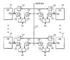
- FIG. 1represents a block diagram or flow chart of a write segment for a system or method to test dies on a semiconductor wafer according to an embodiment.
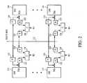
- FIG. 2represents a block diagram or flow chart of a read segment for a system or method to test dies on a semiconductor wafer according to the embodiment in FIG. 1 .
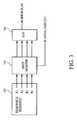
- FIG. 3represents a block diagram or flow chart of a system or method for testing dies on a semiconductor wafer according to another embodiment.
- FIG. 4is a chart illustrating an example of the serial data output from a shift register according to the embodiment in FIG. 3 .
- FIGS. 1 and 2represent block diagrams or flow charts of a testing system or method for dies on a semiconductor wafer according to an embodiment.
- the testing systemwrites data onto part or all of the array in one or more dies of the semiconductor wafer.
- the testing systemreads the data from the die and compares the read data with the original data written onto the array. If the read data is substantially the same as the original or write data, then that portion of the array on the particular die is deemed to have passed the test or have acceptable quality. If the read data is not substantially the same as the original or write data, then that portion of the array on the particular die is deemed to have failed the test or have unacceptable quality.
- the testing systemperforms parallel testing in which the same data is written onto the same portion of the array in each die at essentially the same time. Other testing methods may be used.
- FIG. 1represents a block diagram or flow chart of the write segment of the testing system.
- FIG. 2represents a block diagram or flow chart of the read segment of the testing system along with a portion of the write system shown in FIG. 1 .
- the testing systemuses circuitry and routing mechanisms added to the kerf area or another portion of the semiconductor wafer. Once the testing is completed, the kerf area is cut away from the die.
- the testing systemis used with a testing device (not shown), which provides input signals and receives output signals from the testing system.
- the testing devicehas one or more test pins (not shown) that engage test pads (not shown) on the semiconductor wafer.
- the testing systemmay include a computer or other microprocessor device for performing the test and storing the results.
- the circuitry and routingmay be completely on the wafer.
- the circuitry and routing mechanismmay be partially on the wafer and partially on the testing device. While specific configurations are shown, other configurations may be used including those with fewer or additional components.
- the write segment of the test systemcomprises one or more write registers 102 , 104 , and 106 connected to the selector block 108 .
- the write registers 102 , 104 , and 106are connected to receive a serial input signal from a serial test pin (not shown).
- Selector block 108is connected to receive a select signal from a selector test pin (now shown).
- the testing deviceprovides the serial input and selects signals when engaged to the test pins.
- Selector block 108also is connected to one or more write tristateable buffers 110 via a write bus 112 . Each write tristateable buffer 110 is connected to a die 114 .
- the one or more dies 114collectively form part or all of a semiconductor wafer.
- the dies 114may be arranged as one or more die clusters on the wafer.
- Each write tristateable buffer 110also has a control test pin (not shown) for receiving a write control signal from the testing device.
- the control test pinsmay be interconnected to receive the write control test signal from the testing device through one test pin.
- write bus 112has the same data width as the number of DQ pins in one die. There may be multiple write buses corresponding to the number of die clusters on the semiconductor wafer.
- the read segment of the test systemcomprises one or more pairs of read tristateable buffers 122 and 124 connected to one or more comparators or compressors 126 .
- Each paircomprises a device read tristateable buffer 122 and a bus read tristateable buffer 124 .
- Each device read tristateable buffers 122is connected to the die 114 and the comparator or compressor 126 .
- Each bus read tristateable buffer 124also is connected to the write bus 112 and the comparator or compressor 126 .
- Each read tristateable buffer 122 and 124has a control test pin (not shown) for receiving a read control signal from the testing device.
- the control test pins for the read tristateable buffers 122 and 124may be interconnected to receive the read control signals from the testing device through one test pin.
- each comparator or compressor 126has an output test pin for providing an output signal the testing device. The output test pins may be interconnected to provide the output signals through one test pin to the testing device.
- each comparator or compressor 126is connected to a shift register or other data storage/processing device as described below.
- the testing deviceengages the test pins on the semiconductor wafer.
- the testing deviceprovides or writes the serial input signal to write registers 102 , 104 , and 106 , which hold their respective portions of the serial input signal or data test words.
- the testing deviceprovides all the data test words through one serial input pin.
- the selector block 108sends or writes one or more data words from one or more of the write registers 102 , 104 , and 106 onto the dies 114 via the write bus 112 in response to the select signal from the testing device.
- the select signaldetermines or selects one of the write registers 102 , 104 , and 106 to provide the same data word to each of N the dies 114 .
- the write registermay change during a write sequence so that a data word is written from one write register and then another data word is written from another write register.
- the testing devicesends a write control signal during the write state that enables the write tristateable buffers 110 to electrically connect the bus 112 to the dies 114 .
- the testing devicealso sends another control signal that turns the read tristateable buffers 122 and 124 into Hi-Z state, thus isolating the read segment from the bus 112 and dies 114 .
- the data word on each die 114is read and compared with the data word in the selected write register 102 , 104 , and 106 .
- the testing devicesends a read control signal that enables the read tristateable buffers 122 and 124 to connect electrically the dies 114 and the write bus 112 .
- the testing devicealso sends another control signal that turns the write tristateable buffers 110 into Hi-Z state, thus isolating the bus 112 and hence the write registers from the dies 114 .
- the comparator or compressor 126compares the read data from the die 114 with the expected data from the selected write register 102 , 104 , and 106 .
- the comparison result or output signal Ris provided to the testing device or further processed.
- the result Rmay be compressed to one or more bits with respect to data typology information and test needs. In one aspect, the result R is compressed to one bit, reflecting pass or failure.
- the testing devicerepeats the write-read-comparison cycle according to the testing parameters. There may be one or more cycles. Each cycle may use the same or different data words for the same or different write registers 102 , 104 , and 106 .
- the testing systemmay be used to reduce the number of test or data pins from the testing device to the semiconductor wafer.
- the following examplesillustrate the reduction in data pins. Other reductions may be obtained depending upon the number of test channels for each die, the number of dies, the bits of the comparator result, the number of selection signal and control signal inputs, and/or like factors of the semiconductor wafer and testing device.
- FIG. 3represents a block diagram or flow chart of a system or method for testing dies on a semiconductor wafer according to another embodiment.
- This testing systemcomprises read/write segments 352 , a shift register 354 , and a “AND” gate 356 .
- the read/write segments 352are substantially the same and operate substantially the same as the read and write segments previously described in relation to FIGS. 1 and 2 , except that the results R from the comparators or compressors 126 are provided to shift register 354 .
- the shift register 354 and the AND gate 356may be provided on the kerf area or other portion of the semiconductor wafer.
- the shift registers 354 or the AND gate 356may instead be provided on the testing device.
- the data coming out from the read/write segments 352are entered into the shift register 354 and then are fed or transposed into the AND gate 356 .
- the shift register 354also provides serial data out as described below. If any one of the results R is 0 (where 0 indicates failing), the AND gate 356 outputs an error flag.
- the AND gate 356may be another error detection circuit such as an OR gate, a logic gate, a wired gate, and the like. When the error detection circuit is an OR gate, the OR gate outputs an error flag if any one of the results R is 1 (where 1 indicates failing).
- FIG. 4is a chart illustrating an example of the serial data output from the shift register 354 .
- the serial data outis shown in relation to the die and DQ group numbers and their test results. Other serial data outputs may be obtained including those with different pass or fail indications.
- the shift register 354shifts out the data string at the frequency of N times the test or cycle frequency, where N is the number of bits of the shift register.
- the data stringis used to find or determine the die that failed.
- Four data bitsrepresent the DQs from each die that are generated per address after comparison and compression. If a die cluster has six dies, then 24 bits will be generated per cycle. These data bits are latched in parallel to the shift register.
- the shift registeris clocked at 24 times the test frequency, so that during one write-read-comparison cycle, the 24-bit string is read from the serial data output.
- the frequency of clocking the serial data outmay be higher or lower.
- the frequency of clockingmay be lower by reading at a slower rate or by adding pause cycles.
- the error flagis set to 0 if any of these 24 data bits is 0.
- Each diecorresponds to four data bits in the string. If one of these four bits failed, then the die failed for that read address. When an error is detected as indicated by the error flag, a failed die may be found or determined by the 0's in the serial data output. In addition, the particular DQ group that failed may be identified.
- the 24 data channels from the read segment in FIG. 2are reduced to two test channels.
- the total number of saved channels within each die clusteris about 91 depending upon the number of channels used to implement control signals. In one aspect, the number of channels for the control signals is in the range of about 3-5 channels.
Landscapes
- Engineering & Computer Science (AREA)
- General Engineering & Computer Science (AREA)
- Physics & Mathematics (AREA)
- General Physics & Mathematics (AREA)
- Tests Of Electronic Circuits (AREA)
- Semiconductor Integrated Circuits (AREA)
Abstract
Description
- The present application is a division of U.S. application Ser. No. 10/243,544, filed Sep. 12, 2002, pending.
- The following copending and commonly assigned U.S. patent applications have been filed on the same day as the parent of this application. All of these applications relate to and further describe other aspects of this application and are incorporated by reference in their entirety. U.S. patent application Ser. No. 10/242,894, entitled “SEMICONDUCTOR WAFER TESTING SYSTEM,” Attorney Reference Number 10808/75 (2001 P 18015US), filed on Sep. 12, 2002, and now U.S. Pat. No. 6,888,365; U.S. patent application Ser. No. 10/243,363, entitled “DIE ISOLATION SYSTEM FOR SEMICONDUCTOR WAFER TESTING,” Attorney Reference Number 10808/78 (2001 P 09977US), filed on Sep. 12, 2002, pending.
- This invention generally relates to methods and devices for testing dies on semiconductor wafers. More particularly, this invention relates to methods and devices having circuitry and routing mechanisms in the kerf area for testing dies on a semiconductor wafer.
- Integrated circuits (ICs) typically begin fabrication as a die on a flat, circular substrate or wafer. The die comprises a rectangular portion of the wafer surface and is also known as a chip, circuit, or the like. Each wafer usually is segmented by scribe or saw lines into multiple dies, which typically form essentially identical rectangular circuit patterns. Some dies may be engineering or test dies. Other dies may be edge dies where the wafer does not permit the formation of a complete die along the edge of the wafer. On many wafers, there is a kerf area or area between the dies. The size of the kerf area varies as the number and arrangement of the dies on the wafer varies. When fabrication is completed, the wafer is cut along the saw lines to separate the dies for use in IC devices.
- Dies are tested after fabrication to determine whether a suitable IC has been manufactured. The dies may be individually tested after separation of the wafer. The dies also may be serially tested before separation of the wafer. Die testing usually involves the use of mechanical probes from a testing device. The mechanical probes engage test pads or pins on the die. Once engaged, the testing device applies input signals or voltages to the die then receives output signals or voltages from the die.
- Generally, the testing device needs to have at least the same number of data tester channels as the number of data pins on the die. If a die has eight data pins, then eight data tester channels usually are connected to the eight data pins on the die for reading and writing data. The maximum number of dies that can be tested at the same time is equal to the total number of data tester channels divided by the number of data pins per die.
- This invention provides a testing system or method for comparing read data from one or more dies on a semiconductor wafer with the original data written onto the one or more dies. The testing system uses the comparison of the read data with the write data to determine whether the die passes or fails. In one aspect, the testing system includes a die on a semiconductor wafer, a write register, and a comparator. The write register is connected to the die and writes original data onto the die. The comparator is connected to the die and the write register. The comparator receives read data from the die and receives original data from the write register. The comparator generates a result in response to the original data and the read data.
- In another aspect, the testing system includes one or more dies on a semiconductor wafer, a selector block, one or more write registers, one or more comparators, a shift register, and an error detection circuit. The selector block is connected to the one or more dies and to the one or more write registers. The selector block writes original data from the one or more write registers onto the one or more dies in response to a select signal. The one or more comparators are connected to the one or more dies and the one or more write registers. The one or more comparators receive read data from the one or more dies and receive original data from the one or more write registers. The one or more comparators generate one or more results in response to the original data and the read data. The shift register is connected to receive the one or more results from the one or more comparators. The shift signal generates serial data in response to the one or more results. The error detection circuit is connected to receive the one or more results from the shift register. The error detection circuit may generate an error signal in response to the one or more results.
- In a method for testing dies on a semiconductor wafer, an original data word is written onto one or more dies. A read data word is read from the one or more dies. A result is generated in response to the read data word and the original data word.
- Other systems, methods, features, and advantages of the invention will be or will become apparent to one skilled in the art upon examination of the following figures and detailed description. All such additional systems, methods, features, and advantages are intended to be included within this description, within the scope of the invention, and protected by the accompanying claims.
- The invention may be better understood with reference to the following figures and detailed description. The components in the figures are not necessarily to scale, emphasis being placed upon illustrating the principles of the invention. Moreover, like reference numerals in the figures designate corresponding parts throughout the different views.
FIG. 1 represents a block diagram or flow chart of a write segment for a system or method to test dies on a semiconductor wafer according to an embodiment.FIG. 2 represents a block diagram or flow chart of a read segment for a system or method to test dies on a semiconductor wafer according to the embodiment inFIG. 1 .FIG. 3 represents a block diagram or flow chart of a system or method for testing dies on a semiconductor wafer according to another embodiment.FIG. 4 is a chart illustrating an example of the serial data output from a shift register according to the embodiment inFIG. 3 .FIGS. 1 and 2 represent block diagrams or flow charts of a testing system or method for dies on a semiconductor wafer according to an embodiment. The testing system writes data onto part or all of the array in one or more dies of the semiconductor wafer. The testing system reads the data from the die and compares the read data with the original data written onto the array. If the read data is substantially the same as the original or write data, then that portion of the array on the particular die is deemed to have passed the test or have acceptable quality. If the read data is not substantially the same as the original or write data, then that portion of the array on the particular die is deemed to have failed the test or have unacceptable quality. The testing system performs parallel testing in which the same data is written onto the same portion of the array in each die at essentially the same time. Other testing methods may be used.FIG. 1 represents a block diagram or flow chart of the write segment of the testing system.FIG. 2 represents a block diagram or flow chart of the read segment of the testing system along with a portion of the write system shown inFIG. 1 . The testing system uses circuitry and routing mechanisms added to the kerf area or another portion of the semiconductor wafer. Once the testing is completed, the kerf area is cut away from the die. The testing system is used with a testing device (not shown), which provides input signals and receives output signals from the testing system. The testing device has one or more test pins (not shown) that engage test pads (not shown) on the semiconductor wafer. The testing system may include a computer or other microprocessor device for performing the test and storing the results. The circuitry and routing may be completely on the wafer. The circuitry and routing mechanism may be partially on the wafer and partially on the testing device. While specific configurations are shown, other configurations may be used including those with fewer or additional components.- Referring to
FIG. 1 , the write segment of the test system comprises one or more write registers102,104, and106 connected to theselector block 108. The write registers102,104, and106 are connected to receive a serial input signal from a serial test pin (not shown).Selector block 108 is connected to receive a select signal from a selector test pin (now shown). The testing device provides the serial input and selects signals when engaged to the test pins.Selector block 108 also is connected to one or morewrite tristateable buffers 110 via awrite bus 112. Eachwrite tristateable buffer 110 is connected to adie 114. The one or more dies114 collectively form part or all of a semiconductor wafer. The dies114 may be arranged as one or more die clusters on the wafer. Eachwrite tristateable buffer 110 also has a control test pin (not shown) for receiving a write control signal from the testing device. In one aspect, the control test pins may be interconnected to receive the write control test signal from the testing device through one test pin. In one aspect, writebus 112 has the same data width as the number of DQ pins in one die. There may be multiple write buses corresponding to the number of die clusters on the semiconductor wafer. - Referring to
FIG. 2 , a portion of the write segment fromFIG. 1 is shown includingwrite bus 112, writetristateable buffers 110, and dies114. The read segment of the test system comprises one or more pairs ofread tristateable buffers compressors 126. Each pair comprises a device readtristateable buffer 122 and a bus readtristateable buffer 124. Each device readtristateable buffers 122 is connected to the die114 and the comparator orcompressor 126. Each bus readtristateable buffer 124 also is connected to thewrite bus 112 and the comparator orcompressor 126. Each readtristateable buffer read tristateable buffers read tristateable buffers compressor 126 has an output test pin for providing an output signal the testing device. The output test pins may be interconnected to provide the output signals through one test pin to the testing device. In another aspect, each comparator orcompressor 126 is connected to a shift register or other data storage/processing device as described below. - In operation, the testing device engages the test pins on the semiconductor wafer. During an initialization state or period, the testing device provides or writes the serial input signal to write
registers - During a write state or period, data from one or more of the write registers102,104, and106 are written onto a portion of the array in each of the dies114. The
selector block 108 sends or writes one or more data words from one or more of the write registers102,104, and106 onto the dies114 via thewrite bus 112 in response to the select signal from the testing device. The select signal determines or selects one of the write registers102,104, and106 to provide the same data word to each of N the dies114. There are N signals, (2.sup.N=x, where N is the number of bits and x is the number of the write register or data word to use). The write register may change during a write sequence so that a data word is written from one write register and then another data word is written from another write register. The testing device sends a write control signal during the write state that enables thewrite tristateable buffers 110 to electrically connect thebus 112 to the dies114. The testing device also sends another control signal that turns theread tristateable buffers bus 112 and dies114. - During a read state or period, the data word on each die114 is read and compared with the data word in the selected
write register read tristateable buffers write bus 112. The testing device also sends another control signal that turns thewrite tristateable buffers 110 into Hi-Z state, thus isolating thebus 112 and hence the write registers from the dies114. - The comparator or
compressor 126 compares the read data from thedie 114 with the expected data from the selectedwrite register - The testing system may be used to reduce the number of test or data pins from the testing device to the semiconductor wafer. The following examples illustrate the reduction in data pins. Other reductions may be obtained depending upon the number of test channels for each die, the number of dies, the bits of the comparator result, the number of selection signal and control signal inputs, and/or like factors of the semiconductor wafer and testing device.
Tester Channels Needed for Each Die = 16 Number of Dies = 4 Bits of Comparator Result = 4 Number of Selection and Control Signal Inputs = 5 Data Pin Reduction = (Number of Data Pins Without Testing System) − (Number of Data Pins With Testing System) Data Pin Reduction = [4*(16 − 4)] − [5] Data Pin Reduction = 43 Tester Channel Needed for Each Die = 16 Number of Dies = 6 Bits of Comparator Result = 4 Number of Selection and Control Signal Inputs = 3 Data Pin Reduction = (Number of Data Pins Without Testing System) − (Number of Data Pins With Testing System) Data Pin Reduction = [6*(16 − 4)] − [3] Data Pin Reduction = 69 FIG. 3 represents a block diagram or flow chart of a system or method for testing dies on a semiconductor wafer according to another embodiment. This testing system comprises read/write segments 352, ashift register 354, and a “AND”gate 356. The read/write segments 352 are substantially the same and operate substantially the same as the read and write segments previously described in relation toFIGS. 1 and 2 , except that the results R from the comparators orcompressors 126 are provided to shiftregister 354. Theshift register 354 and the ANDgate 356 may be provided on the kerf area or other portion of the semiconductor wafer. The shift registers354 or the ANDgate 356 may instead be provided on the testing device.- In operation, the data coming out from the read/write segments352 (the results R from the comparators or
compressors 126 inFIG. 2 ) are entered into theshift register 354 and then are fed or transposed into the ANDgate 356. Theshift register 354 also provides serial data out as described below. If any one of the results R is 0 (where 0 indicates failing), the ANDgate 356 outputs an error flag. The ANDgate 356 may be another error detection circuit such as an OR gate, a logic gate, a wired gate, and the like. When the error detection circuit is an OR gate, the OR gate outputs an error flag if any one of the results R is 1 (where 1 indicates failing). FIG. 4 is a chart illustrating an example of the serial data output from theshift register 354. The serial data out is shown in relation to the die and DQ group numbers and their test results. Other serial data outputs may be obtained including those with different pass or fail indications. For each write-read-comparison cycle, theshift register 354 shifts out the data string at the frequency of N times the test or cycle frequency, where N is the number of bits of the shift register. The data string is used to find or determine the die that failed. Four data bits represent the DQs from each die that are generated per address after comparison and compression. If a die cluster has six dies, then 24 bits will be generated per cycle. These data bits are latched in parallel to the shift register. In one aspect, the shift register is clocked at 24 times the test frequency, so that during one write-read-comparison cycle, the 24-bit string is read from the serial data output. The frequency of clocking the serial data out may be higher or lower. The frequency of clocking may be lower by reading at a slower rate or by adding pause cycles. The error flag is set to 0 if any of these 24 data bits is 0. Each die corresponds to four data bits in the string. If one of these four bits failed, then the die failed for that read address. When an error is detected as indicated by the error flag, a failed die may be found or determined by the 0's in the serial data output. In addition, the particular DQ group that failed may be identified. The 24 data channels from the read segment inFIG. 2 are reduced to two test channels. The total number of saved channels within each die cluster is about 91 depending upon the number of channels used to implement control signals. In one aspect, the number of channels for the control signals is in the range of about 3-5 channels.- Various embodiments of the invention have been described and illustrated. However, the description and illustrations are by way of example only. Other embodiments and implementations are possible within the scope of this invention and will be apparent to those of ordinary skill in the art. Therefore, the invention is not limited to the specific details, representative embodiments, and illustrated examples in this description. Accordingly, the invention is not to be restricted except in light as necessitated by the accompanying claims and their equivalents.
Claims (7)
Priority Applications (2)
| Application Number | Priority Date | Filing Date | Title |
|---|---|---|---|
| US11/386,512US7242208B2 (en) | 2002-09-12 | 2006-03-22 | System and method for testing one or more dies on a semiconductor wafer |
| US11/707,408US7449909B2 (en) | 2002-09-12 | 2007-02-16 | System and method for testing one or more dies on a semiconductor wafer |
Applications Claiming Priority (2)
| Application Number | Priority Date | Filing Date | Title |
|---|---|---|---|
| US10/243,544US7119567B2 (en) | 2002-09-12 | 2002-09-12 | System and method for testing one or more dies on a semiconductor wafer |
| US11/386,512US7242208B2 (en) | 2002-09-12 | 2006-03-22 | System and method for testing one or more dies on a semiconductor wafer |
Related Parent Applications (1)
| Application Number | Title | Priority Date | Filing Date |
|---|---|---|---|
| US10/243,544DivisionUS7119567B2 (en) | 2002-09-12 | 2002-09-12 | System and method for testing one or more dies on a semiconductor wafer |
Related Child Applications (1)
| Application Number | Title | Priority Date | Filing Date |
|---|---|---|---|
| US11/707,408ContinuationUS7449909B2 (en) | 2002-09-12 | 2007-02-16 | System and method for testing one or more dies on a semiconductor wafer |
Publications (2)
| Publication Number | Publication Date |
|---|---|
| US20060158209A1true US20060158209A1 (en) | 2006-07-20 |
| US7242208B2 US7242208B2 (en) | 2007-07-10 |
Family
ID=31946387
Family Applications (3)
| Application Number | Title | Priority Date | Filing Date |
|---|---|---|---|
| US10/243,544Expired - Fee RelatedUS7119567B2 (en) | 2002-09-12 | 2002-09-12 | System and method for testing one or more dies on a semiconductor wafer |
| US11/386,512Expired - Fee RelatedUS7242208B2 (en) | 2002-09-12 | 2006-03-22 | System and method for testing one or more dies on a semiconductor wafer |
| US11/707,408Expired - Fee RelatedUS7449909B2 (en) | 2002-09-12 | 2007-02-16 | System and method for testing one or more dies on a semiconductor wafer |
Family Applications Before (1)
| Application Number | Title | Priority Date | Filing Date |
|---|---|---|---|
| US10/243,544Expired - Fee RelatedUS7119567B2 (en) | 2002-09-12 | 2002-09-12 | System and method for testing one or more dies on a semiconductor wafer |
Family Applications After (1)
| Application Number | Title | Priority Date | Filing Date |
|---|---|---|---|
| US11/707,408Expired - Fee RelatedUS7449909B2 (en) | 2002-09-12 | 2007-02-16 | System and method for testing one or more dies on a semiconductor wafer |
Country Status (2)
| Country | Link |
|---|---|
| US (3) | US7119567B2 (en) |
| DE (1) | DE10342275A1 (en) |
Families Citing this family (25)
| Publication number | Priority date | Publication date | Assignee | Title |
|---|---|---|---|---|
| JP4864306B2 (en)* | 2004-09-27 | 2012-02-01 | 富士通セミコンダクター株式会社 | Semiconductor device and test method thereof |
| US7307528B2 (en)* | 2004-12-15 | 2007-12-11 | Impinj, Inc. | RFID tag design with circuitry for wafer level testing |
| US7312622B2 (en)* | 2004-12-15 | 2007-12-25 | Impinj, Inc. | Wafer level testing for RFID tags |
| US7380190B2 (en)* | 2004-12-15 | 2008-05-27 | Impinj, Inc. | RFID tag with bist circuits |
| US7528724B2 (en)* | 2005-02-28 | 2009-05-05 | Impinj, Inc. | On die RFID tag antenna |
| US7400255B2 (en)* | 2005-02-28 | 2008-07-15 | Impinj, Inc. | Wireless functional testing of RFID tag |
| JP2007235108A (en)* | 2006-02-02 | 2007-09-13 | Nec Electronics Corp | Device for testing semiconductor and method of testing semiconductor |
| KR20080069778A (en)* | 2007-01-24 | 2008-07-29 | 삼성전자주식회사 | Test circuit of semiconductor memory device for multichip test and test method thereof |
| US7620861B2 (en)* | 2007-05-31 | 2009-11-17 | Kingtiger Technology (Canada) Inc. | Method and apparatus for testing integrated circuits by employing test vector patterns that satisfy passband requirements imposed by communication channels |
| US7954020B2 (en)* | 2007-06-06 | 2011-05-31 | Sony Computer Entertainment Inc. | Method and apparatus for testing a circuit |
| US7977959B2 (en)* | 2007-09-27 | 2011-07-12 | Formfactor, Inc. | Method and apparatus for testing devices using serially controlled intelligent switches |
| US7757144B2 (en)* | 2007-11-01 | 2010-07-13 | Kingtiger Technology (Canada) Inc. | System and method for testing integrated circuit modules comprising a plurality of integrated circuit devices |
| US7848899B2 (en)* | 2008-06-09 | 2010-12-07 | Kingtiger Technology (Canada) Inc. | Systems and methods for testing integrated circuit devices |
| TWI560456B (en)* | 2009-03-20 | 2016-12-01 | Bravechips Microelectronics | Method of parallel ic test and wafer containing same function dies under test and ic chips containing same function blocks under test |
| US8356215B2 (en)* | 2010-01-19 | 2013-01-15 | Kingtiger Technology (Canada) Inc. | Testing apparatus and method for analyzing a memory module operating within an application system |
| CN102313870B (en)* | 2010-07-05 | 2015-05-06 | 上海芯豪微电子有限公司 | Integrated circuit parallel testing method, device and system |
| WO2012003790A1 (en)* | 2010-07-05 | 2012-01-12 | 上海芯豪微电子有限公司 | Integrated circuit parallel testing method, device, and system |
| US8918686B2 (en) | 2010-08-18 | 2014-12-23 | Kingtiger Technology (Canada) Inc. | Determining data valid windows in a system and method for testing an integrated circuit device |
| FR2965645B1 (en)* | 2010-10-05 | 2012-10-12 | St Microelectronics Grenoble 2 | TEST METHOD FOR SEMICONDUCTOR INTEGRATED ELECTRONIC DEVICES AND CORRESPONDING TEST ARCHITECTURE |
| US9003256B2 (en) | 2011-09-06 | 2015-04-07 | Kingtiger Technology (Canada) Inc. | System and method for testing integrated circuits by determining the solid timing window |
| US8724408B2 (en) | 2011-11-29 | 2014-05-13 | Kingtiger Technology (Canada) Inc. | Systems and methods for testing and assembling memory modules |
| US9117552B2 (en) | 2012-08-28 | 2015-08-25 | Kingtiger Technology(Canada), Inc. | Systems and methods for testing memory |
| FR3033412B1 (en)* | 2015-03-06 | 2019-04-12 | Starchip | INTEGRATED CIRCUIT TESTER ON A SILICON GALETTE AND INTEGRATED CIRCUIT. |
| KR102457825B1 (en) | 2018-04-10 | 2022-10-24 | 에스케이하이닉스 주식회사 | Semiconductor system |
| CN120179870B (en)* | 2025-05-22 | 2025-08-22 | 杭州开幕光子技术有限公司 | A method for storing test data |
Citations (11)
| Publication number | Priority date | Publication date | Assignee | Title |
|---|---|---|---|---|
| US4139818A (en)* | 1977-09-30 | 1979-02-13 | Burroughs Corporation | Circuit means for collecting operational errors in IC chips and for identifying and storing the locations thereof |
| US4340857A (en)* | 1980-04-11 | 1982-07-20 | Siemens Corporation | Device for testing digital circuits using built-in logic block observers (BILBO's) |
| US4956602A (en)* | 1989-02-14 | 1990-09-11 | Amber Engineering, Inc. | Wafer scale testing of redundant integrated circuit dies |
| US5053700A (en)* | 1989-02-14 | 1991-10-01 | Amber Engineering, Inc. | Method for wafer scale testing of redundant integrated circuit dies |
| US5059899A (en)* | 1990-08-16 | 1991-10-22 | Micron Technology, Inc. | Semiconductor dies and wafers and methods for making |
| US5279975A (en)* | 1992-02-07 | 1994-01-18 | Micron Technology, Inc. | Method of testing individual dies on semiconductor wafers prior to singulation |
| US5483175A (en)* | 1992-04-10 | 1996-01-09 | Micron Technology, Inc. | Method for circuits connection for wafer level burning and testing of individual dies on semiconductor wafer |
| US5899703A (en)* | 1997-03-28 | 1999-05-04 | International Business Machines Corporation | Method for chip testing |
| US6046600A (en)* | 1995-10-31 | 2000-04-04 | Texas Instruments Incorporated | Process of testing integrated circuit dies on a wafer |
| US6166557A (en)* | 1996-10-31 | 2000-12-26 | Texas Instruments Incorporated | Process of selecting dies for testing on a wafer |
| US6233184B1 (en)* | 1998-11-13 | 2001-05-15 | International Business Machines Corporation | Structures for wafer level test and burn-in |
Family Cites Families (6)
| Publication number | Priority date | Publication date | Assignee | Title |
|---|---|---|---|---|
| US5720031A (en)* | 1995-12-04 | 1998-02-17 | Micron Technology, Inc. | Method and apparatus for testing memory devices and displaying results of such tests |
| US6452411B1 (en)* | 1999-03-01 | 2002-09-17 | Formfactor, Inc. | Efficient parallel testing of integrated circuit devices using a known good device to generate expected responses |
| JP2001000221A (en) | 1999-06-23 | 2001-01-09 | Itsuo Moriya | Gore wrap-around umbrella |
| JP2001221833A (en)* | 2000-02-09 | 2001-08-17 | Mitsubishi Electric Corp | Wafer and wafer test method |
| US7173444B2 (en)* | 2000-04-04 | 2007-02-06 | Ali Pourkeramati | Structure and method for parallel testing of dies on a semiconductor wafer |
| US6717429B2 (en)* | 2000-06-30 | 2004-04-06 | Texas Instruments Incorporated | IC having comparator inputs connected to core circuitry and output pad |
- 2002
- 2002-09-12USUS10/243,544patent/US7119567B2/ennot_activeExpired - Fee Related
- 2003
- 2003-09-12DEDE10342275Apatent/DE10342275A1/ennot_activeCeased
- 2006
- 2006-03-22USUS11/386,512patent/US7242208B2/ennot_activeExpired - Fee Related
- 2007
- 2007-02-16USUS11/707,408patent/US7449909B2/ennot_activeExpired - Fee Related
Patent Citations (11)
| Publication number | Priority date | Publication date | Assignee | Title |
|---|---|---|---|---|
| US4139818A (en)* | 1977-09-30 | 1979-02-13 | Burroughs Corporation | Circuit means for collecting operational errors in IC chips and for identifying and storing the locations thereof |
| US4340857A (en)* | 1980-04-11 | 1982-07-20 | Siemens Corporation | Device for testing digital circuits using built-in logic block observers (BILBO's) |
| US4956602A (en)* | 1989-02-14 | 1990-09-11 | Amber Engineering, Inc. | Wafer scale testing of redundant integrated circuit dies |
| US5053700A (en)* | 1989-02-14 | 1991-10-01 | Amber Engineering, Inc. | Method for wafer scale testing of redundant integrated circuit dies |
| US5059899A (en)* | 1990-08-16 | 1991-10-22 | Micron Technology, Inc. | Semiconductor dies and wafers and methods for making |
| US5279975A (en)* | 1992-02-07 | 1994-01-18 | Micron Technology, Inc. | Method of testing individual dies on semiconductor wafers prior to singulation |
| US5483175A (en)* | 1992-04-10 | 1996-01-09 | Micron Technology, Inc. | Method for circuits connection for wafer level burning and testing of individual dies on semiconductor wafer |
| US6046600A (en)* | 1995-10-31 | 2000-04-04 | Texas Instruments Incorporated | Process of testing integrated circuit dies on a wafer |
| US6166557A (en)* | 1996-10-31 | 2000-12-26 | Texas Instruments Incorporated | Process of selecting dies for testing on a wafer |
| US5899703A (en)* | 1997-03-28 | 1999-05-04 | International Business Machines Corporation | Method for chip testing |
| US6233184B1 (en)* | 1998-11-13 | 2001-05-15 | International Business Machines Corporation | Structures for wafer level test and burn-in |
Also Published As
| Publication number | Publication date |
|---|---|
| US7242208B2 (en) | 2007-07-10 |
| US20070152700A1 (en) | 2007-07-05 |
| US7449909B2 (en) | 2008-11-11 |
| US20040054951A1 (en) | 2004-03-18 |
| DE10342275A1 (en) | 2004-03-25 |
| US7119567B2 (en) | 2006-10-10 |
Similar Documents
| Publication | Publication Date | Title |
|---|---|---|
| US7242208B2 (en) | System and method for testing one or more dies on a semiconductor wafer | |
| EP1159630B1 (en) | Distributed interface for parallel testing of multiple devices using a single tester channel | |
| US8108741B2 (en) | Semiconductor memory device having mount test circuits and mount test method thereof | |
| US20060195742A1 (en) | Semiconductor memory device and method of testing the same | |
| US5384533A (en) | Testing method, testing circuit and semiconductor integrated circuit having testing circuit | |
| KR20190061957A (en) | Semiconductor device and system including the same | |
| US7134059B2 (en) | Pad connection structure of embedded memory devices and related memory testing method | |
| US7552368B2 (en) | Systems and methods for simultaneously testing semiconductor memory devices | |
| US6915467B2 (en) | System and method for testing a column redundancy of an integrated circuit memory | |
| US8176370B2 (en) | Method and system for direct access memory testing of an integrated circuit | |
| US7412634B2 (en) | On-chip sampling circuit and method | |
| US7376872B1 (en) | Testing embedded memory in integrated circuits such as programmable logic devices | |
| US8201034B2 (en) | Memory device and related testing method | |
| KR100898029B1 (en) | Semiconductor test device and test method | |
| US20080316846A1 (en) | Semiconductor memory device capable of storing data of various patterns and method of electrically testing the semiconductor memory device | |
| KR100771263B1 (en) | Memory array test methods and memory-based devices arranged to implement them | |
| JP5612249B2 (en) | Semiconductor memory device | |
| KR20010027864A (en) | DDR memory device carrying out package parallel bit test by using one data I/O pin | |
| CN113012748A (en) | Repair analysis circuit and memory including the same | |
| US20250216455A1 (en) | Testing circuit for testing electrical devices and device under test | |
| KR100524925B1 (en) | Semiconductor memory device implemented parallel bit test capable of test time and parallel bit test method using the same | |
| KR100732738B1 (en) | Error Decision Circuit in Data Path Compression Mode | |
| JP2002372570A (en) | Multi-chip module and test method thereof | |
| KR20040015589A (en) | Semiconductor memory device with improved test reliability | |
| JPH05307900A (en) | Semiconductor memory device |
Legal Events
| Date | Code | Title | Description |
|---|---|---|---|
| STCF | Information on status: patent grant | Free format text:PATENTED CASE | |
| AS | Assignment | Owner name:QIMONDA AG,GERMANY Free format text:ASSIGNMENT OF ASSIGNORS INTEREST;ASSIGNOR:INFINEON TECHNOLOGIES AG;REEL/FRAME:023768/0001 Effective date:20060425 Owner name:QIMONDA AG, GERMANY Free format text:ASSIGNMENT OF ASSIGNORS INTEREST;ASSIGNOR:INFINEON TECHNOLOGIES AG;REEL/FRAME:023768/0001 Effective date:20060425 | |
| FPAY | Fee payment | Year of fee payment:4 | |
| FPAY | Fee payment | Year of fee payment:8 | |
| AS | Assignment | Owner name:INFINEON TECHNOLOGIES AG, GERMANY Free format text:ASSIGNMENT OF ASSIGNORS INTEREST;ASSIGNOR:QIMONDA AG;REEL/FRAME:035623/0001 Effective date:20141009 | |
| AS | Assignment | Owner name:POLARIS INNOVATIONS LIMITED, IRELAND Free format text:ASSIGNMENT OF ASSIGNORS INTEREST;ASSIGNOR:INFINEON TECHNOLOGIES AG;REEL/FRAME:036818/0583 Effective date:20150708 | |
| FEPP | Fee payment procedure | Free format text:MAINTENANCE FEE REMINDER MAILED (ORIGINAL EVENT CODE: REM.); ENTITY STATUS OF PATENT OWNER: LARGE ENTITY | |
| LAPS | Lapse for failure to pay maintenance fees | Free format text:PATENT EXPIRED FOR FAILURE TO PAY MAINTENANCE FEES (ORIGINAL EVENT CODE: EXP.); ENTITY STATUS OF PATENT OWNER: LARGE ENTITY | |
| STCH | Information on status: patent discontinuation | Free format text:PATENT EXPIRED DUE TO NONPAYMENT OF MAINTENANCE FEES UNDER 37 CFR 1.362 | |
| FP | Lapsed due to failure to pay maintenance fee | Effective date:20190710 |