US20060157795A1 - Structure and method to optimize strain in cmosfets - Google Patents
Structure and method to optimize strain in cmosfetsDownload PDFInfo
- Publication number
- US20060157795A1 US20060157795A1US10/905,745US90574505AUS2006157795A1US 20060157795 A1US20060157795 A1US 20060157795A1US 90574505 AUS90574505 AUS 90574505AUS 2006157795 A1US2006157795 A1US 2006157795A1
- Authority
- US
- United States
- Prior art keywords
- semiconductor device
- strain
- semiconductor
- strain inducing
- inducing coating
- Prior art date
- Legal status (The legal status is an assumption and is not a legal conclusion. Google has not performed a legal analysis and makes no representation as to the accuracy of the status listed.)
- Granted
Links
- 238000000034methodMethods0.000titleclaimsabstractdescription29
- 239000004065semiconductorSubstances0.000claimsabstractdescription96
- 230000001939inductive effectEffects0.000claimsabstractdescription29
- 239000011248coating agentSubstances0.000claimsabstractdescription23
- 238000000576coating methodMethods0.000claimsabstractdescription23
- 229920002120photoresistant polymerPolymers0.000claimsdescription29
- 239000000758substrateSubstances0.000claimsdescription19
- 239000007943implantSubstances0.000claimsdescription14
- 229910052785arsenicInorganic materials0.000claimsdescription11
- 229910052732germaniumInorganic materials0.000claimsdescription10
- 238000005530etchingMethods0.000claimsdescription9
- 238000000151depositionMethods0.000claimsdescription8
- 239000002019doping agentSubstances0.000claimsdescription6
- 229910052581Si3N4Inorganic materials0.000claimsdescription4
- 238000004519manufacturing processMethods0.000claimsdescription4
- 230000005855radiationEffects0.000claimsdescription2
- 150000004767nitridesChemical class0.000abstractdescription61
- 229910052698phosphorusInorganic materials0.000abstractdescription13
- 229910052757nitrogenInorganic materials0.000abstractdescription11
- 229910021420polycrystalline siliconInorganic materials0.000description9
- 229920005591polysiliconPolymers0.000description9
- 125000006850spacer groupChemical group0.000description9
- 230000015556catabolic processEffects0.000description7
- 238000006731degradation reactionMethods0.000description7
- 230000008021depositionEffects0.000description7
- 238000005137deposition processMethods0.000description6
- 239000000463materialSubstances0.000description6
- 239000004020conductorSubstances0.000description5
- VYPSYNLAJGMNEJ-UHFFFAOYSA-NSilicium dioxideChemical compoundO=[Si]=OVYPSYNLAJGMNEJ-UHFFFAOYSA-N0.000description4
- MCMNRKCIXSYSNV-UHFFFAOYSA-NZirconium dioxideChemical compoundO=[Zr]=OMCMNRKCIXSYSNV-UHFFFAOYSA-N0.000description4
- 238000000137annealingMethods0.000description4
- 238000005229chemical vapour depositionMethods0.000description4
- 238000002955isolationMethods0.000description4
- 239000005368silicate glassSubstances0.000description4
- 230000004888barrier functionEffects0.000description3
- 239000003989dielectric materialSubstances0.000description3
- 238000001312dry etchingMethods0.000description3
- 239000012212insulatorSubstances0.000description3
- 238000005468ion implantationMethods0.000description3
- 229910052710siliconInorganic materials0.000description3
- XUIMIQQOPSSXEZ-UHFFFAOYSA-NSiliconChemical compound[Si]XUIMIQQOPSSXEZ-UHFFFAOYSA-N0.000description2
- 229910000577Silicon-germaniumInorganic materials0.000description2
- GWEVSGVZZGPLCZ-UHFFFAOYSA-NTitan oxideChemical compoundO=[Ti]=OGWEVSGVZZGPLCZ-UHFFFAOYSA-N0.000description2
- PNEYBMLMFCGWSK-UHFFFAOYSA-Naluminium oxideInorganic materials[O-2].[O-2].[O-2].[Al+3].[Al+3]PNEYBMLMFCGWSK-UHFFFAOYSA-N0.000description2
- 238000000231atomic layer depositionMethods0.000description2
- 230000015572biosynthetic processEffects0.000description2
- 229910052796boronInorganic materials0.000description2
- 229910052681coesiteInorganic materials0.000description2
- 229910052593corundumInorganic materials0.000description2
- 229910052906cristobaliteInorganic materials0.000description2
- 238000009792diffusion processMethods0.000description2
- 230000008020evaporationEffects0.000description2
- 238000001704evaporationMethods0.000description2
- CJNBYAVZURUTKZ-UHFFFAOYSA-Nhafnium(IV) oxideInorganic materialsO=[Hf]=OCJNBYAVZURUTKZ-UHFFFAOYSA-N0.000description2
- 150000002500ionsChemical class0.000description2
- 238000001459lithographyMethods0.000description2
- 229910052914metal silicateInorganic materials0.000description2
- 239000000203mixtureSubstances0.000description2
- 230000003647oxidationEffects0.000description2
- 238000007254oxidation reactionMethods0.000description2
- 238000005240physical vapour depositionMethods0.000description2
- 238000001020plasma etchingMethods0.000description2
- 229920003209poly(hydridosilsesquioxane)Polymers0.000description2
- 229910021332silicideInorganic materials0.000description2
- FVBUAEGBCNSCDD-UHFFFAOYSA-Nsilicide(4-)Chemical compound[Si-4]FVBUAEGBCNSCDD-UHFFFAOYSA-N0.000description2
- 239000010703siliconSubstances0.000description2
- 239000000377silicon dioxideSubstances0.000description2
- 229910052682stishoviteInorganic materials0.000description2
- 229910052905tridymiteInorganic materials0.000description2
- 229910001845yogo sapphireInorganic materials0.000description2
- ZOXJGFHDIHLPTG-UHFFFAOYSA-NBoronChemical compound[B]ZOXJGFHDIHLPTG-UHFFFAOYSA-N0.000description1
- 229910001218Gallium arsenideInorganic materials0.000description1
- 229910004129HfSiOInorganic materials0.000description1
- 229910000673Indium arsenideInorganic materials0.000description1
- 229910002244LaAlO3Inorganic materials0.000description1
- BPQQTUXANYXVAA-UHFFFAOYSA-NOrthosilicateChemical compound[O-][Si]([O-])([O-])[O-]BPQQTUXANYXVAA-UHFFFAOYSA-N0.000description1
- OAICVXFJPJFONN-UHFFFAOYSA-NPhosphorusChemical compound[P]OAICVXFJPJFONN-UHFFFAOYSA-N0.000description1
- 229910003811SiGeCInorganic materials0.000description1
- 229910002370SrTiO3Inorganic materials0.000description1
- BOTDANWDWHJENH-UHFFFAOYSA-NTetraethyl orthosilicateChemical compoundCCO[Si](OCC)(OCC)OCCBOTDANWDWHJENH-UHFFFAOYSA-N0.000description1
- ATJFFYVFTNAWJD-UHFFFAOYSA-NTinChemical compound[Sn]ATJFFYVFTNAWJD-UHFFFAOYSA-N0.000description1
- 229910052782aluminiumInorganic materials0.000description1
- 229910052787antimonyInorganic materials0.000description1
- 229910052797bismuthInorganic materials0.000description1
- YZYDPPZYDIRSJT-UHFFFAOYSA-Kboron phosphateChemical compound[B+3].[O-]P([O-])([O-])=OYZYDPPZYDIRSJT-UHFFFAOYSA-K0.000description1
- 229910000149boron phosphateInorganic materials0.000description1
- 238000000224chemical solution depositionMethods0.000description1
- 230000000295complement effectEffects0.000description1
- 150000001875compoundsChemical class0.000description1
- 238000007796conventional methodMethods0.000description1
- 230000005669field effectEffects0.000description1
- -1for exampleChemical class0.000description1
- 229910052733galliumInorganic materials0.000description1
- 238000011065in-situ storageMethods0.000description1
- 229910052738indiumInorganic materials0.000description1
- RPQDHPTXJYYUPQ-UHFFFAOYSA-Nindium arsenideChemical compound[In]#[As]RPQDHPTXJYYUPQ-UHFFFAOYSA-N0.000description1
- 239000011810insulating materialSubstances0.000description1
- 238000010884ion-beam techniqueMethods0.000description1
- MRELNEQAGSRDBK-UHFFFAOYSA-Nlanthanum oxideInorganic materials[O-2].[O-2].[O-2].[La+3].[La+3]MRELNEQAGSRDBK-UHFFFAOYSA-N0.000description1
- 238000000608laser ablationMethods0.000description1
- 239000002184metalSubstances0.000description1
- 229910052751metalInorganic materials0.000description1
- 229910044991metal oxideInorganic materials0.000description1
- 150000004706metal oxidesChemical class0.000description1
- 229910003465moissaniteInorganic materials0.000description1
- KTUFCUMIWABKDW-UHFFFAOYSA-Noxo(oxolanthaniooxy)lanthanumChemical compoundO=[La]O[La]=OKTUFCUMIWABKDW-UHFFFAOYSA-N0.000description1
- 239000011574phosphorusSubstances0.000description1
- 238000000623plasma-assisted chemical vapour depositionMethods0.000description1
- 238000005546reactive sputteringMethods0.000description1
- 229910010271silicon carbideInorganic materials0.000description1
- 229910052716thalliumInorganic materials0.000description1
- 238000001039wet etchingMethods0.000description1
Images

Classifications
- H—ELECTRICITY
- H10—SEMICONDUCTOR DEVICES; ELECTRIC SOLID-STATE DEVICES NOT OTHERWISE PROVIDED FOR
- H10D—INORGANIC ELECTRIC SEMICONDUCTOR DEVICES
- H10D30/00—Field-effect transistors [FET]
- H10D30/60—Insulated-gate field-effect transistors [IGFET]
- H10D30/791—Arrangements for exerting mechanical stress on the crystal lattice of the channel regions
- H10D30/792—Arrangements for exerting mechanical stress on the crystal lattice of the channel regions comprising applied insulating layers, e.g. stress liners
- H—ELECTRICITY
- H10—SEMICONDUCTOR DEVICES; ELECTRIC SOLID-STATE DEVICES NOT OTHERWISE PROVIDED FOR
- H10D—INORGANIC ELECTRIC SEMICONDUCTOR DEVICES
- H10D84/00—Integrated devices formed in or on semiconductor substrates that comprise only semiconducting layers, e.g. on Si wafers or on GaAs-on-Si wafers
- H10D84/01—Manufacture or treatment
- H10D84/0123—Integrating together multiple components covered by H10D12/00 or H10D30/00, e.g. integrating multiple IGBTs
- H10D84/0126—Integrating together multiple components covered by H10D12/00 or H10D30/00, e.g. integrating multiple IGBTs the components including insulated gates, e.g. IGFETs
- H10D84/0165—Integrating together multiple components covered by H10D12/00 or H10D30/00, e.g. integrating multiple IGBTs the components including insulated gates, e.g. IGFETs the components including complementary IGFETs, e.g. CMOS devices
- H10D84/0167—Manufacturing their channels
- H—ELECTRICITY
- H10—SEMICONDUCTOR DEVICES; ELECTRIC SOLID-STATE DEVICES NOT OTHERWISE PROVIDED FOR
- H10D—INORGANIC ELECTRIC SEMICONDUCTOR DEVICES
- H10D84/00—Integrated devices formed in or on semiconductor substrates that comprise only semiconducting layers, e.g. on Si wafers or on GaAs-on-Si wafers
- H10D84/01—Manufacture or treatment
- H10D84/0123—Integrating together multiple components covered by H10D12/00 or H10D30/00, e.g. integrating multiple IGBTs
- H10D84/0126—Integrating together multiple components covered by H10D12/00 or H10D30/00, e.g. integrating multiple IGBTs the components including insulated gates, e.g. IGFETs
- H10D84/0165—Integrating together multiple components covered by H10D12/00 or H10D30/00, e.g. integrating multiple IGBTs the components including insulated gates, e.g. IGFETs the components including complementary IGFETs, e.g. CMOS devices
- H10D84/0172—Manufacturing their gate conductors
- H10D84/0177—Manufacturing their gate conductors the gate conductors having different materials or different implants
- H—ELECTRICITY
- H10—SEMICONDUCTOR DEVICES; ELECTRIC SOLID-STATE DEVICES NOT OTHERWISE PROVIDED FOR
- H10D—INORGANIC ELECTRIC SEMICONDUCTOR DEVICES
- H10D84/00—Integrated devices formed in or on semiconductor substrates that comprise only semiconducting layers, e.g. on Si wafers or on GaAs-on-Si wafers
- H10D84/01—Manufacture or treatment
- H10D84/02—Manufacture or treatment characterised by using material-based technologies
- H10D84/03—Manufacture or treatment characterised by using material-based technologies using Group IV technology, e.g. silicon technology or silicon-carbide [SiC] technology
- H10D84/038—Manufacture or treatment characterised by using material-based technologies using Group IV technology, e.g. silicon technology or silicon-carbide [SiC] technology using silicon technology, e.g. SiGe
- H—ELECTRICITY
- H01—ELECTRIC ELEMENTS
- H01L—SEMICONDUCTOR DEVICES NOT COVERED BY CLASS H10
- H01L2924/00—Indexing scheme for arrangements or methods for connecting or disconnecting semiconductor or solid-state bodies as covered by H01L24/00
- H01L2924/0001—Technical content checked by a classifier
- H01L2924/0002—Not covered by any one of groups H01L24/00, H01L24/00 and H01L2224/00
Definitions
- the present inventionrelates generally to a semiconductor structure of strained complementary metal oxide semiconductor field effect transistors (CMOSFETs), and a method for fabricating strained MOSFETs that optimizes strain in the MOSFETs, and more particularly pertains to a structure and method that maximizes the strain in one type/kind (N or P) of MOSFET and minimizes and relaxes the strain in another type/kind (P or N) of MOSFET.
- CMOSFETscomplementary metal oxide semiconductor field effect transistors
- compressive CA nitrideimproves the performance of PMOSFETs while it degrades the performance of NMOSFETs
- tensile CA nitrideimproves the performance of NMOSFETs while it degrades the performance of PMOSFETs.
- the compressive nitride film or tensile nitride filmcan be selectively deposited by changing the power of the plasma deposition, as is known in the art.
- Masked (blocked PFET or blocked NFET) Ge or As implantshave been implemented to relax the stress in one kind (N or P) of MOSFET to reduce the degradation while maintaining the strain in another kind (P or N) of MOSFET.
- a thick CA nitridecan cause higher stress in the channel of one kind (N or P) of MOSFET.
- a thick CA nitridemakes it harder to relax the stress with Ge or As implants to improve the performance of the other kind (P or N) MOSFET.
- the present inventionprovides a structure and method to optimize strain in semiconductor devices such as CMOSFETs and has broad applicability to semiconductor devices in general.
- the subject inventionprovides a strained semiconductor structure comprising both PMOSFETs and NMOSFETS, and a method for fabricating strained MOSFETs that maximizes the strain in one type/kind (P or N) of MOSFET and minimizes and relaxes the strain in another type/kind (N or P) of MOSFET.
- a strain inducing CA nitride coating having an original full thicknessis formed over one of the PMOSFET and the NMOSFET, wherein the strain inducing coating produces an optimized full strain in the one semiconductor device.
- a strain inducing CA nitride coating having an etched reduced thickness, less than the full thickness,is formed over the other of the PMOSFET and the NMOSFET, wherein the reduced thickness of the strain inducing coating relaxes and produces less strain in the other MOSFET.
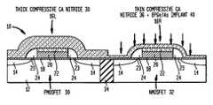
- FIG. 1illustrates a MOSFET structure having a greater thickness of CA compressive nitride on a PMOSFET that maximizes the strain in the PMOSFET and a lesser thickness of CA compressive nitride on an NMOSFET that minimizes and relaxes the strain in the NMOSFET.
- FIG. 2illustrates a MOSFET structure having a greater thickness of CA tensile nitride on an NMOSFET that maximizes the strain in the NMOSFET and a lesser thickness of CA tensile nitride on a PMOSFET that minimizes and relaxes the strain in the PMOSFET.
- the present inventionprovides a MOSFET structure with different thicknesses of contact barrier (CA) nitride on NMOSFETs and PMOSFETs that maximizes the strain in one type/kind (P or N) of MOSFET and minimizes and relaxes the strain in another type/kind (Nor P) of MOSFET.
- CAcontact barrier
- FIG. 1illustrates first and second exemplary embodiments of the present invention on a semiconductor wafer having both PMOSFETs 30 and NMOSFETs 32 separated by isolation regions 34 .
- compressive CA nitrideis used to maximize the strain in the PMOSFETs 30 and minimize and relax the strain in the NMOSFETs 32 .
- the waferis patterned with photoresist such that the PMOSFETs 30 are covered by photoresist and the NMOSFETs 32 are exposed and not covered by photoresist.
- the CA nitride at the NMOSFETs 32is etched thinner at 38 to (300-500 A), while the photoresist protects the PMOSFETs 30 from the etch.
- FIG. 1also illustrates that a Ge or As implant 40 can be applied to further relax the strain and improve the NMOSFETs 32 performance.
- a thick (700-1000 A) layer of compressive CA nitride 36is deposited on both the PMOSFETs 30 and the NMOSFETs 32 on a wafer.
- a blanket layer of photoresistis then deposited over the wafer, and the photoresist is then patterned by using a mask such that the PMOSFETs 30 are covered by photoresist while the NMOSFETs 32 remain exposed and are not covered by the photoresist.
- the CA nitride at the NMOSFETs 32is then etched thinner to (300-500 A) at 38 , while the photoresist protects the CA nitride at the PMOSFETs 30 from the etch such that the CA nitride 36 on top of the PMOSFETs 30 remains at the full deposited thickness. Therefore, the thinner CA nitride at 38 on top of the NMOSFETs 32 results in less compressive strain at the NMOSFETs 32 than at the PMOSFETs 30 , and the degradation of the NMOSFETs 32 caused by the compressive CA nitride is reduced.
- FIG. 1also illustrates a second embodiment wherein, after completion of the above steps, the NMOSFETs 32 degradation is further reduced by implanting at 40 Ge or As into the NMOSFETs 32 .
- the implant 40is performed while the PMOSFETs 30 are blocked with a mask, (indicated in the drawing by +B (block) P (PFETs) Ge/As implant 40 ), which can be the same mask used to pattern the photoresist, to further relax the strain and improve the performance of the NMOSFETs 32 .
- FIG. 2illustrates third and fourth exemplary embodiments of the present invention which show that the same structure and method of FIG. 1 can be applied to tensile CA nitride.
- the waferis patterned with photoresist such that the NMOSFETs 32 are covered by photoresist while the PMOSFETs 30 are exposed and not covered by photoresist.
- the CA nitride at the PMOSFETs 30is etched thinner at 44 to (300-500 A), while the photoresist protects the NMOSFETs 32 from the etch.
- FIG. 2also illustrates at 46 that a Ge or As implant can be applied to further relax the strain and improve the PMOSFETs 30 performance.
- a thick (700-1000 A) layer of tensile CA nitride 42is deposited on both the PMOSFETs 30 and the NMOSFETs 32 on the wafer.
- the waferis then patterned with photoresist by using a mask such that the NMOSFETs 32 are covered by photoresist and the PMOSFETs 30 remain exposed and are not covered by photoresist.
- the CA nitride at the PMOSFETs 30is then etched thinner to (300-500 A) at 44 , while the photoresist protects the CA nitride 42 at the NMOSFETs 34 from the etch such that the CA nitride remains at the full original thickness. Therefore, the thinner CA nitride 44 at the PMOSFETs 30 results in less tensile strain at the PMOSFETs 30 than at the NMOSFETs 32 , and the degradation of the PMOSFETs 30 caused by the tensile CA nitride is reduced.
- FIG. 2also illustrates a fourth embodiment wherein, after completion of the above steps, the PMOSFETs 30 degradation is further reduced by implanting at 46 Ge or As into the PMOSFETs 30 .
- the implant 46is performed while the NMOSFETs 32 are blocked with a mask (indicated in the drawing by +B (block) N (NFETs) Ge/As implant), which can be the same mask used to pattern the photoresist, to further relax the strain and improve the performance of the PMOSFETs 30 .
- the compressive nitride film or tensile nitride filmcan be selectively deposited by changing the power of the plasma deposition, as is known in the art.
- the stress inducing film of the present inventioncan comprise a nitride, preferably Si 3 N 4 , or alternatively TiN, an oxide, a doped oxide such as boron phosphate silicate glass, Al 2 O 3 , HfO 2 , ZrO 2 , HfSiO, and other dielectric materials that are common to semiconductor processing or any combination thereof.
- the stress inducing filmcan have a thickness ranging from about 10 nm to about 100 nm.
- the stress inducing filmprovides a compressive stress in the device channel to improve pFET performance or provides a tensile stress in the device channel to improve nFET performance.
- FIG. 10show an IC structure 10 having two MOSFET device regions formed atop a single semiconductor substrate. Although illustration is made to such an embodiment, the present invention is not limited to the formation of any specific number of MOSFET devices on the surface of the semiconductor structure.
- the IC structure 10includes a semiconductor substrate 12 , source/drain regions 14 located within the semiconductor substrate 12 , and two left and right gate regions 16 L and 16 R which are located on the surface of the semiconductor substrate 12 .
- Each gate region 16 L and 16 Rincludes a gate dielectric 18 , a polySi conductor 20 , a dielectric cap 22 , a dielectric liner 23 , spacers 24 and source/drain regions 14 located within the semiconductor substrate 12 .
- the semiconductor substrate 12 of structure 10can comprise any semiconducting material including, but not limited to: Si, Ge, SiGe, SiC, SiGeC, Ga, GaAs, InAs, InP and all other III/V compound semiconductors.
- Semiconductor substrate 12may also comprise an organic semiconductor or a layered semiconductor such as Si/SiGe, a silicon-on-insulator (SOI) or a SiGe-on-insulator (SGOI).
- SOIsilicon-on-insulator
- SGOISiGe-on-insulator
- the semiconductor substrate 12may be doped, undoped or contain doped and undoped regions therein.
- the semiconductor substrate 12may also include a first doped (n- or p-) region, and a second doped (n- or p-) region. These doped regions are known as “wells”.
- the first doped region and the second doped regionmay be the same, or they may have different conductivities and/or doping concentrations.
- Trench isolation regions 34are typically already formed in the semiconductor substrate at this point of the present invention utilizing conventional processes well known to those skilled in the art.
- the trench isolation regionsare located to the left and right peripheries of the region shown in the drawings of the present invention as well as between the two gate regions as depicted.
- a gate dielectric 18is formed on the entire surface of the structure 10 including the semiconductor substrate 12 and atop the isolation region, if it is present and if it is a deposited dielectric.
- the gate dielectric 18can be formed by a thermal growing process such as, for example, oxidation, nitridation or oxynitridation.
- the gate dielectric 18can be formed by a deposition process such as, for example, chemical vapor deposition (CVD), plasma-assisted CVD, atomic layer deposition (ALD), evaporation, reactive sputtering, chemical solution deposition and other like deposition processes.
- the gate dielectric 18may also be formed utilizing any combination of the above processes.
- the gate dielectric 18is comprised of an insulating material including, but not limited to: an oxide, nitride, oxynitride and/or silicate including metal silicates and nitrided metal silicates. In one embodiment, it is preferred that the gate dielectric 18 is comprised of an oxide such as, for example, SiO 2 , HfO 2 , ZrO 2 , Al 2 O 3 , TiO 2 , La 2 O 3 , SrTiO 3 , LaAlO 3 , and mixtures thereof.
- the physical thickness of the gate dielectric 18may vary, but typically, the gate dielectric 18 has a thickness from about 0.5 to about 10 nm, with a thickness from about 0.5 to about 3 nm being more typical.
- a blanket layer of polysilicon(i.e., polySi) which becomes the polySi gate conductor 20 shown in the drawings is formed on the gate dielectric 18 utilizing a known deposition process such as, for example, physical vapor deposition, CVD or evaporation.
- the blanket layer of polysiliconmay be doped or undoped. If doped, an in-situ doping deposition process may be employed in forming the same.
- a doped polySi layercan be formed by deposition, ion implantation and annealing. The doping of the polySi layer will shift the workfunction of the silicided metal gate formed.
- dopant ionsinclude As, P, B, Sb, Bi, In, Al, Ga, Tl or mixtures thereof.
- the thickness, i.e., height, of the polysilicon layer deposited at this point of the present inventionmay vary depending on the deposition process employed. Typically, the polysilicon layer has a vertical thickness from about 20 to about 180 nm, with a thickness from about 40 to about 150 nm being more typical.
- a dielectric cap 22is formed atop the blanket layer of polysilicon gate conductor 20 utilizing a deposition process such as, for example, physical vapor deposition or chemical vapor deposition.
- the dielectric cap 22may be an oxide, nitride, oxynitride or any combination thereof.
- the dielectric cap 22can be comprised of a different dielectric material than spacer 24 to be defined in detail herein below.
- a nitridesuch as, for example, Si 3 N 4
- the dielectric cap 22is an oxide such as SiO 2 .
- the thickness, i.e., height, of the dielectric cap 22is from about 20 to about 180 nm, with a thickness from about 30 to about 140 nm being more typical.
- the blanket polysilicon layer and dielectric cap layerare then patterned by lithography and etching so as to provide patterned gate stacks.
- the patterned gate stacksmay have the same dimension, i.e., length, or they can have variable dimensions to improve device performance.
- Each patterned gate stack at this point of the present inventionincludes a polySi gate conductor 20 and a dielectric cap 22 .
- the lithography stepincludes applying a photoresist to the upper surface of the dielectric cap layer, exposing the photoresist to a desired pattern of radiation and developing the exposed photoresist utilizing a conventional resist developer.
- the pattern in the photoresistis then transferred to the dielectric cap layer and the blanket layer of polysilicon utilizing one or more dry etching steps.
- the patterned photoresistmay be removed after the pattern has been transferred into the dielectric cap layer. In other embodiments, the patterned photoresist is removed after etching has been completed.
- a dielectric liner 23is formed on all exposed surfaces containing silicon including at least the polysilicon gate conductor 20 .
- the dielectric liner 23can also extend onto horizontal surfaces of the semiconductor substrate 12 .
- the dielectric liner 23may comprise any dielectric material that contains an oxide, nitride, oxynitride or any combination thereof.
- the dielectric liner 23is formed via a thermal growing process such as oxidation, nitridation or oxynitridation.
- the dielectric liner 23is a thin layer whose thickness is typically from about 1 to about 10 nm.
- source/drain diffusion regions 14are formed into the substrate 12 at the exposed portions.
- the source/drain diffusion regions 14are formed utilizing ion implantation and an annealing step.
- the annealing stepserves to activate the dopants that were implanted by the previous implant step.
- the conditions for the ion implantation and annealingare well known to those skilled in the art.
- the thick compressive or tensile CA nitride film 30 or 42is formed over the entire structure shown in FIGS. 1 and 2 and further fabrication and processing proceeds as described in detail above to form the thin compressive or tensile CA nitride film 36 or 44 , and possibly the GE/As implant 40 or 46 .
- a planarizing dielectric layer(not shown) can be formed.
- the planarizing dielectric layercomprises an oxide such as a high density oxide or an oxide deposited from TEOS.
- the planarizing dielectric layermay comprise a doped silicate glass, such as boron doped silicate glass (BSG) or phosphorus doped silicate glass (PSG), a spin-coatable polymeric material such as hydrogen silsesquioxane (HSQ), or a photoresist.
- BSGboron doped silicate glass
- PSGphosphorus doped silicate glass
- HSQhydrogen silsesquioxane
- the planarizing dielectric layeris formed by conventional techniques well known to those skilled in the art.
- the thickness of the planarizing dielectric layer formed at this pointmay vary depending on the type of material employed. Typically, the planarizing dielectric layer has a thickness from about 50 to about 100 nm.
Landscapes
- Insulated Gate Type Field-Effect Transistor (AREA)
- Metal-Oxide And Bipolar Metal-Oxide Semiconductor Integrated Circuits (AREA)
- Thin Film Transistor (AREA)
- Electrodes Of Semiconductors (AREA)
- Internal Circuitry In Semiconductor Integrated Circuit Devices (AREA)
Abstract
Description
- The present invention relates generally to a semiconductor structure of strained complementary metal oxide semiconductor field effect transistors (CMOSFETs), and a method for fabricating strained MOSFETs that optimizes strain in the MOSFETs, and more particularly pertains to a structure and method that maximizes the strain in one type/kind (N or P) of MOSFET and minimizes and relaxes the strain in another type/kind (P or N) of MOSFET.
- Process induced strain has attracted a great deal of attention recently because the strain can enhance the carrier mobility in the channel of a MOSFET. Contact barrier (CA) nitride stress engineering is especially effective in transferring strain into the channel of a MOSFET. Moreover, the process is compatible with and can be easily implemented in the current manufacturing process. The strain in the channel of a MOSFET is proportional to the thickness of the contact barrier (CA) nitride, with a thicker CA nitride causing higher stress in the channel of the MOSFET. Either compressive CA nitride or tensile CA nitride can improve the performance of one kind of MOSFET and degrade the performance of another kind of MOSFET. More specifically, compressive CA nitride improves the performance of PMOSFETs while it degrades the performance of NMOSFETs, and tensile CA nitride improves the performance of NMOSFETs while it degrades the performance of PMOSFETs. The compressive nitride film or tensile nitride film can be selectively deposited by changing the power of the plasma deposition, as is known in the art.
- Masked (blocked PFET or blocked NFET) Ge or As implants have been implemented to relax the stress in one kind (N or P) of MOSFET to reduce the degradation while maintaining the strain in another kind (P or N) of MOSFET. A thick CA nitride can cause higher stress in the channel of one kind (N or P) of MOSFET. However, a thick CA nitride makes it harder to relax the stress with Ge or As implants to improve the performance of the other kind (P or N) MOSFET.
- The present invention provides a structure and method to optimize strain in semiconductor devices such as CMOSFETs and has broad applicability to semiconductor devices in general. The subject invention provides a strained semiconductor structure comprising both PMOSFETs and NMOSFETS, and a method for fabricating strained MOSFETs that maximizes the strain in one type/kind (P or N) of MOSFET and minimizes and relaxes the strain in another type/kind (N or P) of MOSFET.
- A strain inducing CA nitride coating having an original full thickness is formed over one of the PMOSFET and the NMOSFET, wherein the strain inducing coating produces an optimized full strain in the one semiconductor device. A strain inducing CA nitride coating having an etched reduced thickness, less than the full thickness, is formed over the other of the PMOSFET and the NMOSFET, wherein the reduced thickness of the strain inducing coating relaxes and produces less strain in the other MOSFET.
- The foregoing objects and advantages of the present invention for structure and method to optimize strain in MOSFETs may be more readily understood by one skilled in the art with reference being had to the following detailed description of several embodiments thereof, taken in conjunction with the accompanying drawings wherein like elements are designated by identical reference numerals throughout the several views, and in which:
FIG. 1 illustrates a MOSFET structure having a greater thickness of CA compressive nitride on a PMOSFET that maximizes the strain in the PMOSFET and a lesser thickness of CA compressive nitride on an NMOSFET that minimizes and relaxes the strain in the NMOSFET.FIG. 2 illustrates a MOSFET structure having a greater thickness of CA tensile nitride on an NMOSFET that maximizes the strain in the NMOSFET and a lesser thickness of CA tensile nitride on a PMOSFET that minimizes and relaxes the strain in the PMOSFET.- The present invention provides a MOSFET structure with different thicknesses of contact barrier (CA) nitride on NMOSFETs and PMOSFETs that maximizes the strain in one type/kind (P or N) of MOSFET and minimizes and relaxes the strain in another type/kind (Nor P) of MOSFET.
FIG. 1 illustrates first and second exemplary embodiments of the present invention on a semiconductor wafer having bothPMOSFETs 30 andNMOSFETs 32 separated byisolation regions 34. In the first and second exemplary embodiments of the present invention, compressive CA nitride is used to maximize the strain in thePMOSFETs 30 and minimize and relax the strain in theNMOSFETs 32.- In summary, after deposition of a thick (700-1000 A)
compressive CA nitride 36 on both thePMOSFETs 30 and theNMOSFETs 32, the wafer is patterned with photoresist such that thePMOSFETs 30 are covered by photoresist and theNMOSFETs 32 are exposed and not covered by photoresist. The CA nitride at theNMOSFETs 32 is etched thinner at38 to (300-500 A), while the photoresist protects thePMOSFETs 30 from the etch. Therefore, the thinner CA nitride38 at theNMOSFETs 32 results in less compressive strain at theNMOSFETs 32 than at thePMOSFETs 30, and theNMOSFETs 32 degradation is reduced.FIG. 1 also illustrates that a Ge or Asimplant 40 can be applied to further relax the strain and improve theNMOSFETs 32 performance. - In a first step, a thick (700-1000 A) layer of
compressive CA nitride 36 is deposited on both thePMOSFETs 30 and theNMOSFETs 32 on a wafer. - A blanket layer of photoresist is then deposited over the wafer, and the photoresist is then patterned by using a mask such that the
PMOSFETs 30 are covered by photoresist while theNMOSFETs 32 remain exposed and are not covered by the photoresist. - The CA nitride at the
NMOSFETs 32 is then etched thinner to (300-500 A) at38, while the photoresist protects the CA nitride at thePMOSFETs 30 from the etch such that theCA nitride 36 on top of thePMOSFETs 30 remains at the full deposited thickness. Therefore, the thinner CA nitride at38 on top of theNMOSFETs 32 results in less compressive strain at theNMOSFETs 32 than at thePMOSFETs 30, and the degradation of theNMOSFETs 32 caused by the compressive CA nitride is reduced. - The first embodiment of the present invention is completed with the completion of the above steps.
FIG. 1 also illustrates a second embodiment wherein, after completion of the above steps, theNMOSFETs 32 degradation is further reduced by implanting at40 Ge or As into theNMOSFETs 32. Theimplant 40 is performed while the PMOSFETs30 are blocked with a mask, (indicated in the drawing by +B (block) P (PFETs) Ge/As implant40), which can be the same mask used to pattern the photoresist, to further relax the strain and improve the performance of theNMOSFETs 32. FIG. 2 illustrates third and fourth exemplary embodiments of the present invention which show that the same structure and method ofFIG. 1 can be applied to tensile CA nitride. In summary, after deposition of a thick (700-1000 A)tensile CA nitride 42 on both theNMOSFETs 32 and thePMOSFETs 30, the wafer is patterned with photoresist such that theNMOSFETs 32 are covered by photoresist while thePMOSFETs 30 are exposed and not covered by photoresist. The CA nitride at the PMOSFETs30 is etched thinner at44 to (300-500 A), while the photoresist protects theNMOSFETs 32 from the etch. Therefore, thethinner CA nitride 44 at thePMOSFETs 30 results in less compressive strain at thePMOSFETs 30 than at theNMOSFETs 32, and thePMOSFETs 30 degradation is reduced.FIG. 2 also illustrates at46 that a Ge or As implant can be applied to further relax the strain and improve the PMOSFETs30 performance.- In a first step a thick (700-1000 A) layer of
tensile CA nitride 42 is deposited on both thePMOSFETs 30 and theNMOSFETs 32 on the wafer. - The wafer is then patterned with photoresist by using a mask such that the
NMOSFETs 32 are covered by photoresist and thePMOSFETs 30 remain exposed and are not covered by photoresist. - The CA nitride at the
PMOSFETs 30 is then etched thinner to (300-500 A) at44, while the photoresist protects theCA nitride 42 at theNMOSFETs 34 from the etch such that the CA nitride remains at the full original thickness. Therefore, thethinner CA nitride 44 at thePMOSFETs 30 results in less tensile strain at thePMOSFETs 30 than at theNMOSFETs 32, and the degradation of thePMOSFETs 30 caused by the tensile CA nitride is reduced. - The third embodiment of the present invention is completed with the completion of the above steps.
FIG. 2 also illustrates a fourth embodiment wherein, after completion of the above steps, thePMOSFETs 30 degradation is further reduced by implanting at46 Ge or As into thePMOSFETs 30. Theimplant 46 is performed while the NMOSFETs32 are blocked with a mask (indicated in the drawing by +B (block) N (NFETs) Ge/As implant), which can be the same mask used to pattern the photoresist, to further relax the strain and improve the performance of thePMOSFETs 30. - The process conditions for the implant to relax the strain in the nitride film can be:
- As or GE
- Dose: 5e14 to 2e15
- Energy: 20 K to 50 K
- The exact implant conditions depend upon the film thickness, and the stress in the film.
- The compressive nitride film or tensile nitride film can be selectively deposited by changing the power of the plasma deposition, as is known in the art.
- In alternative embodiments, other stress materials can be used in the present invention instead of the nitride film, but the nitride film has an advantage in conformity. The stress inducing film of the present invention can comprise a nitride, preferably Si3N4, or alternatively TiN, an oxide, a doped oxide such as boron phosphate silicate glass, Al2O3, HfO2, ZrO2, HfSiO, and other dielectric materials that are common to semiconductor processing or any combination thereof. The stress inducing film can have a thickness ranging from about 10 nm to about 100 nm. The stress inducing film provides a compressive stress in the device channel to improve pFET performance or provides a tensile stress in the device channel to improve nFET performance.
- The drawings show an
IC structure 10 having two MOSFET device regions formed atop a single semiconductor substrate. Although illustration is made to such an embodiment, the present invention is not limited to the formation of any specific number of MOSFET devices on the surface of the semiconductor structure. - In a more detailed explanation of the fabrication process, the
IC structure 10 includes asemiconductor substrate 12, source/drain regions 14 located within thesemiconductor substrate 12, and two left andright gate regions semiconductor substrate 12. Eachgate region polySi conductor 20, adielectric cap 22, adielectric liner 23,spacers 24 and source/drain regions 14 located within thesemiconductor substrate 12. - The
semiconductor substrate 12 ofstructure 10 can comprise any semiconducting material including, but not limited to: Si, Ge, SiGe, SiC, SiGeC, Ga, GaAs, InAs, InP and all other III/V compound semiconductors.Semiconductor substrate 12 may also comprise an organic semiconductor or a layered semiconductor such as Si/SiGe, a silicon-on-insulator (SOI) or a SiGe-on-insulator (SGOI). In some embodiments of the present invention, it is preferred that thesemiconductor substrate 12 be composed of a Si-containing semiconductor material, i.e., a semiconductor material that includes silicon. Thesemiconductor substrate 12 may be doped, undoped or contain doped and undoped regions therein. - The
semiconductor substrate 12 may also include a first doped (n- or p-) region, and a second doped (n- or p-) region. These doped regions are known as “wells”. The first doped region and the second doped region may be the same, or they may have different conductivities and/or doping concentrations. Trench isolation regions 34 are typically already formed in the semiconductor substrate at this point of the present invention utilizing conventional processes well known to those skilled in the art. The trench isolation regions are located to the left and right peripheries of the region shown in the drawings of the present invention as well as between the two gate regions as depicted.- A
gate dielectric 18 is formed on the entire surface of thestructure 10 including thesemiconductor substrate 12 and atop the isolation region, if it is present and if it is a deposited dielectric. Thegate dielectric 18 can be formed by a thermal growing process such as, for example, oxidation, nitridation or oxynitridation. Alternatively, thegate dielectric 18 can be formed by a deposition process such as, for example, chemical vapor deposition (CVD), plasma-assisted CVD, atomic layer deposition (ALD), evaporation, reactive sputtering, chemical solution deposition and other like deposition processes. Thegate dielectric 18 may also be formed utilizing any combination of the above processes. - The
gate dielectric 18 is comprised of an insulating material including, but not limited to: an oxide, nitride, oxynitride and/or silicate including metal silicates and nitrided metal silicates. In one embodiment, it is preferred that thegate dielectric 18 is comprised of an oxide such as, for example, SiO2, HfO2, ZrO2, Al2O3, TiO2, La2O3, SrTiO3, LaAlO3, and mixtures thereof. - The physical thickness of the
gate dielectric 18 may vary, but typically, thegate dielectric 18 has a thickness from about 0.5 to about 10 nm, with a thickness from about 0.5 to about 3 nm being more typical. - After forming the
gate dielectric 18, a blanket layer of polysilicon (i.e., polySi) which becomes thepolySi gate conductor 20 shown in the drawings is formed on thegate dielectric 18 utilizing a known deposition process such as, for example, physical vapor deposition, CVD or evaporation. The blanket layer of polysilicon may be doped or undoped. If doped, an in-situ doping deposition process may be employed in forming the same. Alternatively, a doped polySi layer can be formed by deposition, ion implantation and annealing. The doping of the polySi layer will shift the workfunction of the silicided metal gate formed. Illustrative examples of dopant ions include As, P, B, Sb, Bi, In, Al, Ga, Tl or mixtures thereof. Typical doses for the ion implants are 1E14 (=1×10¹⁴) to 1E16 (=1×10¹⁶) atoms/cm2or more typically 1E15 to 5E15 atoms/cm2. The thickness, i.e., height, of the polysilicon layer deposited at this point of the present invention may vary depending on the deposition process employed. Typically, the polysilicon layer has a vertical thickness from about 20 to about 180 nm, with a thickness from about 40 to about 150 nm being more typical. - After deposition of the blanket layer of polysilicon, a
dielectric cap 22 is formed atop the blanket layer ofpolysilicon gate conductor 20 utilizing a deposition process such as, for example, physical vapor deposition or chemical vapor deposition. Thedielectric cap 22 may be an oxide, nitride, oxynitride or any combination thereof. Thedielectric cap 22 can be comprised of a different dielectric material thanspacer 24 to be defined in detail herein below. In one embodiment, a nitride such as, for example, Si3N4, is employed as thedielectric cap 22. In yet another embodiment, which is preferred, thedielectric cap 22 is an oxide such as SiO2. The thickness, i.e., height, of thedielectric cap 22 is from about 20 to about 180 nm, with a thickness from about 30 to about 140 nm being more typical. - The blanket polysilicon layer and dielectric cap layer are then patterned by lithography and etching so as to provide patterned gate stacks. The patterned gate stacks may have the same dimension, i.e., length, or they can have variable dimensions to improve device performance. Each patterned gate stack at this point of the present invention includes a
polySi gate conductor 20 and adielectric cap 22. The lithography step includes applying a photoresist to the upper surface of the dielectric cap layer, exposing the photoresist to a desired pattern of radiation and developing the exposed photoresist utilizing a conventional resist developer. The pattern in the photoresist is then transferred to the dielectric cap layer and the blanket layer of polysilicon utilizing one or more dry etching steps. In some embodiments, the patterned photoresist may be removed after the pattern has been transferred into the dielectric cap layer. In other embodiments, the patterned photoresist is removed after etching has been completed. - Suitable dry etching processes that can be used in the present invention in forming the patterned gate stacks include, but are not limited to: reactive ion etching, ion beam etching, plasma etching or laser ablation. The dry etching process employed is typically selective to the
underlying gate dielectric 18 therefore this etching step does not typically remove the gate dielectric. In some embodiments, this etching step may however be used to remove portions of thegate dielectric 18 that are not protected by the gate stacks. A wet etching process can also be used to remove portions of thegate dielectric 18 that are not protected by the gate stacks. - Next, a
dielectric liner 23 is formed on all exposed surfaces containing silicon including at least thepolysilicon gate conductor 20. Thedielectric liner 23 can also extend onto horizontal surfaces of thesemiconductor substrate 12. Thedielectric liner 23 may comprise any dielectric material that contains an oxide, nitride, oxynitride or any combination thereof. Thedielectric liner 23 is formed via a thermal growing process such as oxidation, nitridation or oxynitridation. Thedielectric liner 23 is a thin layer whose thickness is typically from about 1 to about 10 nm. - At least one
spacer 24 is formed on exposed sidewalls of each patterned gate stack as well as atop the dielectric liner. The at least onespacer 24 is comprised of an insulator such as an oxide, nitride, oxynitride and/or any combination thereof and it typically is composed of a different material than thedielectric liner 23 and thedielectric cap 22. Preferably, nitride spacers are formed. The at least onespacer 24 is formed by deposition and etching. Note that the etching step used in forming thespacers 24 also can removedielectric liner 23 from atop the substrate such that a portion of thesemiconductor substrate 12 is exposed. - The width of the
spacer 24 must be sufficiently wide such that the source and drain silicide contacts (to be subsequently formed) do not encroach underneath the edges of the gate stack. Typically, the source/drain silicide does not encroach underneath the edges of the gate stack when the spacer has a width, as measured at the bottom, from about 15 to about 80 nm. - After spacer formation, source/
drain diffusion regions 14 are formed into thesubstrate 12 at the exposed portions. The source/drain diffusion regions 14 are formed utilizing ion implantation and an annealing step. The annealing step serves to activate the dopants that were implanted by the previous implant step. The conditions for the ion implantation and annealing are well known to those skilled in the art. - Next, as shown in
FIGS. 1 and 2 , the thick compressive or tensileCA nitride film FIGS. 1 and 2 and further fabrication and processing proceeds as described in detail above to form the thin compressive or tensileCA nitride film implant - After fabricating the structures shown in
FIGS. 1 and 2 , a planarizing dielectric layer (not shown) can be formed. The planarizing dielectric layer comprises an oxide such as a high density oxide or an oxide deposited from TEOS. Alternatively, the planarizing dielectric layer may comprise a doped silicate glass, such as boron doped silicate glass (BSG) or phosphorus doped silicate glass (PSG), a spin-coatable polymeric material such as hydrogen silsesquioxane (HSQ), or a photoresist. The planarizing dielectric layer is formed by conventional techniques well known to those skilled in the art. The thickness of the planarizing dielectric layer formed at this point may vary depending on the type of material employed. Typically, the planarizing dielectric layer has a thickness from about 50 to about 100 nm. - While several embodiments and variations of the present invention for a structure and method to optimize strain in CMOSFETs are described in detail herein, it should be apparent that the disclosure and teachings of the present invention will suggest many alternative designs to those skilled in the art.
Claims (18)
1. A method of fabricating a semiconductor structure having a p-semiconductor device and an n-semiconductor device with different amounts of strain in the p-semiconductor device and the n-semiconductor device comprising:
forming a p-semiconductor device and an n-semiconductor device on a substrate;
forming a strain inducing coating having an original thickness over the p-semiconductor device and also over the n-semiconductor device, wherein the strain inducing coating produces strain in the p-semiconductor device and also in the n-semiconductor device;
protecting one of the strain inducing coated p-semiconductor device and strain inducing coated n-semiconductor device while the other strain inducing coated semiconductor device remains exposed;
etching the exposed strain inducing coating to reduce the thickness of the strain inducing coating to relax the strain in the exposed semiconductor device, while the strain inducing coating over the protected semiconductor device remains protected such that the strain in the protected semiconductor device remains unchanged.
2. The method ofclaim 1 , wherein following the etching, implanting a strain reducing dopant into the exposed semiconductor device to further relax the strain in the exposed semiconductor device.
3. The method ofclaim 2 , including implanting a strain reducing dopant comprising As or Ge.
4. The method ofclaim 3 , including implanting the As or Ge at a dosage of approximately 5e14 atoms/cm2to approximately 2e15 atoms/cm2at an implant energy of approximately 20 KeV to about 50 KeV.
5. The method ofclaim 1 , wherein said step of protecting comprises:
blanket depositing a photoresist layer over the p-semiconductor device and the n-semiconductor device on the substrate;
exposing the photoresist layer to a pattern of radiation and developing the pattern into the photoresist layer to provide a block mask overlying the protected semiconductor device.
6. The method ofclaim 1 , wherein said strain inducing coating provides a compressive strain to improve the performance of the protected p-semiconductor device and the compressive strain is relaxed in the exposed n-semiconductor device.
7. The method ofclaim 6 , wherein the p-semiconductor device is a p-type MOSFET and the n-semiconductor device is an n-type MOSFET.
8. The method ofclaim 1 , wherein said strain inducing coating provides a tensile strain to improve the performance of the protected n-semiconductor device and the compressive strain is relaxed in the exposed p-semiconductor device.
9. The method ofclaim 8 , wherein the p-semiconductor device is a p-type MOSFET and the n-semiconductor device is an n-type MOSFET.
10. The method ofclaim 1 , wherein the strain inducing coating comprises Si3N4.
11. A semiconductor structure comprising a p-semiconductor device and an n-semiconductor device having different amounts of strain in the p-semiconductor device and the n-semiconductor device, comprising:
the semiconductor structure comprising a p-semiconductor device and an n-semiconductor device formed on a substrate;
a strain inducing coating having an original full thickness formed over one of the p-semiconductor device and the n-semiconductor device, wherein the strain inducing coating produces an optimized full strain in the one semiconductor device;
a strain inducing coating having an etched reduced thickness, less than the full thickness, formed over the other of the p-semiconductor device and the n-semiconductor device, wherein the reduced thickness of the strain inducing coating relaxes and produces less strain in the other semiconductor device than in the one semiconductor device.
12. The semiconductor structure ofclaim 11 , wherein the other semiconductor device also has an implanted strain reducing dopant to further relax the strain in the other semiconductor device.
13. The semiconductor structure ofclaim 12 , wherein the implanted strain reducing dopant comprises As or Ge to further relax the strain in the other semiconductor device.
14. The semiconductor structure ofclaim 11 , wherein the strain inducing coating provides a compressive strain to improve the performance of the one p-semiconductor device and the compressive strain is relaxed in the other n-semiconductor device.
15. The semiconductor structure ofclaim 11 , wherein the p-semiconductor device is a p-type MOSFET and the n-semiconductor device is an n-type MOSFET.
16. The semiconductor structure ofclaim 11 , wherein the strain inducing coating provides a tensile strain to improve the performance of the one n-semiconductor device and the compressive strain is relaxed in the other p-semiconductor device.
17. The semiconductor structure ofclaim 11 , wherein the p-semiconductor device is a p-type MOSFET and the n-semiconductor device is an n-type MOSFET.
18. The semiconductor structure ofclaim 11 , wherein the strain inducing coating comprises Si3N4.
Priority Applications (8)
| Application Number | Priority Date | Filing Date | Title |
|---|---|---|---|
| US10/905,745US7432553B2 (en) | 2005-01-19 | 2005-01-19 | Structure and method to optimize strain in CMOSFETs |
| TW095101578ATW200634926A (en) | 2005-01-19 | 2006-01-16 | Structure and method to optimize strain in CMOSFETs |
| CN200680002466.9ACN101496176A (en) | 2005-01-19 | 2006-01-19 | Structure and method to optimize strain in CMOSFET |
| PCT/US2006/001768WO2006078740A2 (en) | 2005-01-19 | 2006-01-19 | Structure and method to optimize strain in cmosfets |
| JP2007552237AJP4884397B2 (en) | 2005-01-19 | 2006-01-19 | Method for optimizing distortion in a CMOSFET |
| EP06718789AEP1842239A4 (en) | 2005-01-19 | 2006-01-19 | STRUCTURE AND METHOD FOR OPTIMIZING STRESS IN CMOS TRANSISTORS |
| US11/928,976US20080070357A1 (en) | 2005-01-19 | 2007-10-30 | STRUCTURE AND METHOD TO OPTIMIZE STRAIN IN CMOSFETs |
| US12/144,800US20080251853A1 (en) | 2005-01-19 | 2008-06-24 | STRUCTURE AND METHOD TO OPTIMIZE STRAIN IN CMOSFETs |
Applications Claiming Priority (1)
| Application Number | Priority Date | Filing Date | Title |
|---|---|---|---|
| US10/905,745US7432553B2 (en) | 2005-01-19 | 2005-01-19 | Structure and method to optimize strain in CMOSFETs |
Related Child Applications (2)
| Application Number | Title | Priority Date | Filing Date |
|---|---|---|---|
| US11/928,976DivisionUS20080070357A1 (en) | 2005-01-19 | 2007-10-30 | STRUCTURE AND METHOD TO OPTIMIZE STRAIN IN CMOSFETs |
| US12/144,800DivisionUS20080251853A1 (en) | 2005-01-19 | 2008-06-24 | STRUCTURE AND METHOD TO OPTIMIZE STRAIN IN CMOSFETs |
Publications (2)
| Publication Number | Publication Date |
|---|---|
| US20060157795A1true US20060157795A1 (en) | 2006-07-20 |
| US7432553B2 US7432553B2 (en) | 2008-10-07 |
Family
ID=36683015
Family Applications (3)
| Application Number | Title | Priority Date | Filing Date |
|---|---|---|---|
| US10/905,745Active2026-02-13US7432553B2 (en) | 2005-01-19 | 2005-01-19 | Structure and method to optimize strain in CMOSFETs |
| US11/928,976AbandonedUS20080070357A1 (en) | 2005-01-19 | 2007-10-30 | STRUCTURE AND METHOD TO OPTIMIZE STRAIN IN CMOSFETs |
| US12/144,800AbandonedUS20080251853A1 (en) | 2005-01-19 | 2008-06-24 | STRUCTURE AND METHOD TO OPTIMIZE STRAIN IN CMOSFETs |
Family Applications After (2)
| Application Number | Title | Priority Date | Filing Date |
|---|---|---|---|
| US11/928,976AbandonedUS20080070357A1 (en) | 2005-01-19 | 2007-10-30 | STRUCTURE AND METHOD TO OPTIMIZE STRAIN IN CMOSFETs |
| US12/144,800AbandonedUS20080251853A1 (en) | 2005-01-19 | 2008-06-24 | STRUCTURE AND METHOD TO OPTIMIZE STRAIN IN CMOSFETs |
Country Status (6)
| Country | Link |
|---|---|
| US (3) | US7432553B2 (en) |
| EP (1) | EP1842239A4 (en) |
| JP (1) | JP4884397B2 (en) |
| CN (1) | CN101496176A (en) |
| TW (1) | TW200634926A (en) |
| WO (1) | WO2006078740A2 (en) |
Cited By (27)
| Publication number | Priority date | Publication date | Assignee | Title |
|---|---|---|---|---|
| US20060223290A1 (en)* | 2005-04-01 | 2006-10-05 | International Business Machines Corporation | Method of producing highly strained pecvd silicon nitride thin films at low temperature |
| US20060281239A1 (en)* | 2005-06-14 | 2006-12-14 | Suraj Mathew | CMOS fabrication |
| US20070013070A1 (en)* | 2005-06-23 | 2007-01-18 | Liang Mong S | Semiconductor devices and methods of manufacture thereof |
| US20070082439A1 (en)* | 2005-10-07 | 2007-04-12 | Samsung Electronics Co., Ltd. | Semiconductor device having a dual stress liner, method of manufacturing the semiconductor device and light exposure apparatus for forming the dual stress liner |
| US20070131964A1 (en)* | 2005-12-13 | 2007-06-14 | Sang Yong Lee | Semiconductor device and method for manufacturing the same |
| US20070235823A1 (en)* | 2006-03-30 | 2007-10-11 | Ju-Wang Hsu | CMOS devices with improved gap-filling |
| US20080048271A1 (en)* | 2006-08-25 | 2008-02-28 | International Business Machines Corporation | STRUCTURE AND METHOD TO USE LOW k STRESS LINER TO REDUCE PARASITIC CAPACITANCE |
| US20080185655A1 (en)* | 2007-02-02 | 2008-08-07 | United Microelectronics Corp. | Smiconductor device, method for fabricating thereof and method for increasing film stress |
| US20080185661A1 (en)* | 2007-02-01 | 2008-08-07 | Shinji Takeoka | Semiconductor device and method for fabricating the same |
| US20080203485A1 (en)* | 2007-02-28 | 2008-08-28 | International Business Machines Corporation | Strained metal gate structure for cmos devices with improved channel mobility and methods of forming the same |
| US20080277726A1 (en)* | 2007-05-08 | 2008-11-13 | Doris Bruce B | Devices with Metal Gate, High-k Dielectric, and Butted Electrodes |
| US20090068824A1 (en)* | 2007-09-11 | 2009-03-12 | United Microelectronics Corp. | Fabricating method of semiconductor device |
| US20090095991A1 (en)* | 2007-10-11 | 2009-04-16 | International Business Machines Corporation | Method of forming strained mosfet devices using phase transformable materials |
| US7541632B2 (en) | 2005-06-14 | 2009-06-02 | Micron Technology, Inc. | Relaxed-pitch method of aligning active area to digit line |
| US7566620B2 (en) | 2005-07-25 | 2009-07-28 | Micron Technology, Inc. | DRAM including a vertical surround gate transistor |
| US20090206410A1 (en)* | 2008-02-20 | 2009-08-20 | Nec Electronics Corporation | Semiconductor device and method for manufacturing the same |
| US7601595B2 (en) | 2005-07-06 | 2009-10-13 | Micron Technology, Inc. | Surround gate access transistors with grown ultra-thin bodies |
| US20090302391A1 (en)* | 2008-06-05 | 2009-12-10 | Chartered Semiconductor Manufacturing, Ltd. | Stress liner for stress engineering |
| US7687342B2 (en) | 2005-09-01 | 2010-03-30 | Micron Technology, Inc. | Method of manufacturing a memory device |
| US7696567B2 (en) | 2005-08-31 | 2010-04-13 | Micron Technology, Inc | Semiconductor memory device |
| US7939409B2 (en) | 2005-09-01 | 2011-05-10 | Micron Technology, Inc. | Peripheral gate stacks and recessed array gates |
| US7977236B2 (en) | 2005-09-01 | 2011-07-12 | Micron Technology, Inc. | Method of forming a transistor gate of a recessed access device, method of forming a recessed transistor gate and a non-recessed transistor gate, and method of fabricating an integrated circuit |
| US8084826B2 (en) | 2008-02-13 | 2011-12-27 | Panasonic Corporation | Semiconductor device and manufacturing method thereof |
| US9082875B2 (en) | 2009-03-27 | 2015-07-14 | International Business Machines Corporation | Methods for normalizing strain in semicondcutor devices and strain normalized semiconductor devices |
| US20160141243A1 (en)* | 2014-11-19 | 2016-05-19 | Samsung Electronics Co., Ltd. | Semiconductor device and method for fabricating the same |
| EP3503203A1 (en)* | 2017-12-22 | 2019-06-26 | Commissariat à l'Energie Atomique et aux Energies Alternatives | Production of transistors with stressed channels |
| US10515801B2 (en) | 2007-06-04 | 2019-12-24 | Micron Technology, Inc. | Pitch multiplication using self-assembling materials |
Families Citing this family (9)
| Publication number | Priority date | Publication date | Assignee | Title |
|---|---|---|---|---|
| US7589385B2 (en)* | 2005-07-26 | 2009-09-15 | United Microelectronics Corp. | Semiconductor CMOS transistors and method of manufacturing the same |
| JP2008066484A (en)* | 2006-09-06 | 2008-03-21 | Fujitsu Ltd | CMOS semiconductor device and manufacturing method thereof |
| JP2008131023A (en)* | 2006-11-27 | 2008-06-05 | Nec Electronics Corp | Semiconductor device and manufacturing method thereof |
| US20080315317A1 (en)* | 2007-06-22 | 2008-12-25 | Chartered Semiconductor Manufacturing Ltd. | Semiconductor system having complementary strained channels |
| US7727834B2 (en)* | 2008-02-14 | 2010-06-01 | Toshiba America Electronic Components, Inc. | Contact configuration and method in dual-stress liner semiconductor device |
| US7795679B2 (en)* | 2008-07-24 | 2010-09-14 | International Business Machines Corporation | Device structures with a self-aligned damage layer and methods for forming such device structures |
| US8389300B2 (en)* | 2010-04-02 | 2013-03-05 | Centre National De La Recherche Scientifique | Controlling ferroelectricity in dielectric films by process induced uniaxial strain |
| US8673757B2 (en) | 2010-10-28 | 2014-03-18 | International Business Machines Corporation | Structure and method for using high-k material as an etch stop layer in dual stress layer process |
| US9159633B2 (en) | 2013-09-13 | 2015-10-13 | Globalfoundries Inc. | Test macro for use with a multi-patterning lithography process |
Citations (70)
| Publication number | Priority date | Publication date | Assignee | Title |
|---|---|---|---|---|
| US3602841A (en)* | 1970-06-18 | 1971-08-31 | Ibm | High frequency bulk semiconductor amplifiers and oscillators |
| US4665415A (en)* | 1985-04-24 | 1987-05-12 | International Business Machines Corporation | Semiconductor device with hole conduction via strained lattice |
| US4853076A (en)* | 1983-12-29 | 1989-08-01 | Massachusetts Institute Of Technology | Semiconductor thin films |
| US4855245A (en)* | 1985-09-13 | 1989-08-08 | Siemens Aktiengesellschaft | Method of manufacturing integrated circuit containing bipolar and complementary MOS transistors on a common substrate |
| US4952524A (en)* | 1989-05-05 | 1990-08-28 | At&T Bell Laboratories | Semiconductor device manufacture including trench formation |
| US4958213A (en)* | 1987-12-07 | 1990-09-18 | Texas Instruments Incorporated | Method for forming a transistor base region under thick oxide |
| US5006913A (en)* | 1988-11-05 | 1991-04-09 | Mitsubishi Denki Kabushiki Kaisha | Stacked type semiconductor device |
| US5060030A (en)* | 1990-07-18 | 1991-10-22 | Raytheon Company | Pseudomorphic HEMT having strained compensation layer |
| US5081513A (en)* | 1991-02-28 | 1992-01-14 | Xerox Corporation | Electronic device with recovery layer proximate to active layer |
| US5108843A (en)* | 1988-11-30 | 1992-04-28 | Ricoh Company, Ltd. | Thin film semiconductor and process for producing the same |
| US5134085A (en)* | 1991-11-21 | 1992-07-28 | Micron Technology, Inc. | Reduced-mask, split-polysilicon CMOS process, incorporating stacked-capacitor cells, for fabricating multi-megabit dynamic random access memories |
| US5310446A (en)* | 1990-01-10 | 1994-05-10 | Ricoh Company, Ltd. | Method for producing semiconductor film |
| US5354695A (en)* | 1992-04-08 | 1994-10-11 | Leedy Glenn J | Membrane dielectric isolation IC fabrication |
| US5371399A (en)* | 1991-06-14 | 1994-12-06 | International Business Machines Corporation | Compound semiconductor having metallic inclusions and devices fabricated therefrom |
| US5391510A (en)* | 1992-02-28 | 1995-02-21 | International Business Machines Corporation | Formation of self-aligned metal gate FETs using a benignant removable gate material during high temperature steps |
| US5459346A (en)* | 1988-06-28 | 1995-10-17 | Ricoh Co., Ltd. | Semiconductor substrate with electrical contact in groove |
| US5557122A (en)* | 1995-05-12 | 1996-09-17 | Alliance Semiconductors Corporation | Semiconductor electrode having improved grain structure and oxide growth properties |
| US5561302A (en)* | 1994-09-26 | 1996-10-01 | Motorola, Inc. | Enhanced mobility MOSFET device and method |
| US5670798A (en)* | 1995-03-29 | 1997-09-23 | North Carolina State University | Integrated heterostructures of Group III-V nitride semiconductor materials including epitaxial ohmic contact non-nitride buffer layer and methods of fabricating same |
| US5679965A (en)* | 1995-03-29 | 1997-10-21 | North Carolina State University | Integrated heterostructures of Group III-V nitride semiconductor materials including epitaxial ohmic contact, non-nitride buffer layer and methods of fabricating same |
| US5861651A (en)* | 1997-02-28 | 1999-01-19 | Lucent Technologies Inc. | Field effect devices and capacitors with improved thin film dielectrics and method for making same |
| US5880040A (en)* | 1996-04-15 | 1999-03-09 | Macronix International Co., Ltd. | Gate dielectric based on oxynitride grown in N2 O and annealed in NO |
| US5940736A (en)* | 1997-03-11 | 1999-08-17 | Lucent Technologies Inc. | Method for forming a high quality ultrathin gate oxide layer |
| US5960297A (en)* | 1997-07-02 | 1999-09-28 | Kabushiki Kaisha Toshiba | Shallow trench isolation structure and method of forming the same |
| US5989978A (en)* | 1998-07-16 | 1999-11-23 | Chartered Semiconductor Manufacturing, Ltd. | Shallow trench isolation of MOSFETS with reduced corner parasitic currents |
| US6008126A (en)* | 1992-04-08 | 1999-12-28 | Elm Technology Corporation | Membrane dielectric isolation IC fabrication |
| US6025280A (en)* | 1997-04-28 | 2000-02-15 | Lucent Technologies Inc. | Use of SiD4 for deposition of ultra thin and controllable oxides |
| US6066545A (en)* | 1997-12-09 | 2000-05-23 | Texas Instruments Incorporated | Birdsbeak encroachment using combination of wet and dry etch for isolation nitride |
| US6090684A (en)* | 1998-07-31 | 2000-07-18 | Hitachi, Ltd. | Method for manufacturing semiconductor device |
| US6107143A (en)* | 1998-03-02 | 2000-08-22 | Samsung Electronics Co., Ltd. | Method for forming a trench isolation structure in an integrated circuit |
| US6117722A (en)* | 1999-02-18 | 2000-09-12 | Taiwan Semiconductor Manufacturing Company | SRAM layout for relaxing mechanical stress in shallow trench isolation technology and method of manufacture thereof |
| US6133071A (en)* | 1997-10-15 | 2000-10-17 | Nec Corporation | Semiconductor device with plate heat sink free from cracks due to thermal stress and process for assembling it with package |
| US6165383A (en)* | 1998-04-10 | 2000-12-26 | Organic Display Technology | Useful precursors for organic electroluminescent materials and devices made from such materials |
| US6221735B1 (en)* | 2000-02-15 | 2001-04-24 | Philips Semiconductors, Inc. | Method for eliminating stress induced dislocations in CMOS devices |
| US6228694B1 (en)* | 1999-06-28 | 2001-05-08 | Intel Corporation | Method of increasing the mobility of MOS transistors by use of localized stress regions |
| US6255169B1 (en)* | 1999-02-22 | 2001-07-03 | Advanced Micro Devices, Inc. | Process for fabricating a high-endurance non-volatile memory device |
| US6261964B1 (en)* | 1997-03-14 | 2001-07-17 | Micron Technology, Inc. | Material removal method for forming a structure |
| US6265317B1 (en)* | 2001-01-09 | 2001-07-24 | Taiwan Semiconductor Manufacturing Company | Top corner rounding for shallow trench isolation |
| US20010009784A1 (en)* | 1998-01-09 | 2001-07-26 | Yanjun Ma | Structure and method of making a sub-micron MOS transistor |
| US6274444B1 (en)* | 1999-07-30 | 2001-08-14 | United Microelectronics Corp. | Method for forming mosfet |
| US6281532B1 (en)* | 1999-06-28 | 2001-08-28 | Intel Corporation | Technique to obtain increased channel mobilities in NMOS transistors by gate electrode engineering |
| US6284623B1 (en)* | 1999-10-25 | 2001-09-04 | Peng-Fei Zhang | Method of fabricating semiconductor devices using shallow trench isolation with reduced narrow channel effect |
| US6284626B1 (en)* | 1999-04-06 | 2001-09-04 | Vantis Corporation | Angled nitrogen ion implantation for minimizing mechanical stress on side walls of an isolation trench |
| US6319794B1 (en)* | 1998-10-14 | 2001-11-20 | International Business Machines Corporation | Structure and method for producing low leakage isolation devices |
| US6361885B1 (en)* | 1998-04-10 | 2002-03-26 | Organic Display Technology | Organic electroluminescent materials and device made from such materials |
| US6362082B1 (en)* | 1999-06-28 | 2002-03-26 | Intel Corporation | Methodology for control of short channel effects in MOS transistors |
| US6368931B1 (en)* | 2000-03-27 | 2002-04-09 | Intel Corporation | Thin tensile layers in shallow trench isolation and method of making same |
| US6403486B1 (en)* | 2001-04-30 | 2002-06-11 | Taiwan Semiconductor Manufacturing Company | Method for forming a shallow trench isolation |
| US6403975B1 (en)* | 1996-04-09 | 2002-06-11 | Max-Planck Gesellschaft Zur Forderung Der Wissenschafteneev | Semiconductor components, in particular photodetectors, light emitting diodes, optical modulators and waveguides with multilayer structures grown on silicon substrates |
| US6406973B1 (en)* | 1999-06-29 | 2002-06-18 | Hyundai Electronics Industries Co., Ltd. | Transistor in a semiconductor device and method of manufacturing the same |
| US20020086472A1 (en)* | 2000-12-29 | 2002-07-04 | Brian Roberds | Technique to obtain high mobility channels in MOS transistors by forming a strain layer on an underside of a channel |
| US20020086497A1 (en)* | 2000-12-30 | 2002-07-04 | Kwok Siang Ping | Beaker shape trench with nitride pull-back for STI |
| US20020090791A1 (en)* | 1999-06-28 | 2002-07-11 | Brian S. Doyle | Method for reduced capacitance interconnect system using gaseous implants into the ild |
| US6461936B1 (en)* | 2002-01-04 | 2002-10-08 | Infineon Technologies Ag | Double pullback method of filling an isolation trench |
| US6476462B2 (en)* | 1999-12-28 | 2002-11-05 | Texas Instruments Incorporated | MOS-type semiconductor device and method for making same |
| US6493497B1 (en)* | 2000-09-26 | 2002-12-10 | Motorola, Inc. | Electro-optic structure and process for fabricating same |
| US6498358B1 (en)* | 2001-07-20 | 2002-12-24 | Motorola, Inc. | Structure and method for fabricating an electro-optic system having an electrochromic diffraction grating |
| US6501121B1 (en)* | 2000-11-15 | 2002-12-31 | Motorola, Inc. | Semiconductor structure |
| US6506652B2 (en)* | 1998-11-13 | 2003-01-14 | Intel Corporation | Method of recessing spacers to improved salicide resistance on polysilicon gates |
| US20030032261A1 (en)* | 2001-08-08 | 2003-02-13 | Ling-Yen Yeh | Method of preventing threshold voltage of MOS transistor from being decreased by shallow trench isolation formation |
| US20030040158A1 (en)* | 2001-08-21 | 2003-02-27 | Nec Corporation | Semiconductor device and method of fabricating the same |
| US6531369B1 (en)* | 2000-03-01 | 2003-03-11 | Applied Micro Circuits Corporation | Heterojunction bipolar transistor (HBT) fabrication using a selectively deposited silicon germanium (SiGe) |
| US6531740B2 (en)* | 2001-07-17 | 2003-03-11 | Motorola, Inc. | Integrated impedance matching and stability network |
| US20030057184A1 (en)* | 2001-09-22 | 2003-03-27 | Shiuh-Sheng Yu | Method for pull back SiN to increase rounding effect in a shallow trench isolation process |
| US20030067035A1 (en)* | 2001-09-28 | 2003-04-10 | Helmut Tews | Gate processing method with reduced gate oxide corner and edge thinning |
| US20040175872A1 (en)* | 2003-03-07 | 2004-09-09 | Taiwan Semiconductor Manufacturing Company | Strain balanced structure with a tensile strained silicon channel and a compressive strained silicon-germanium channel for CMOS performance enhancement |
| US20040195623A1 (en)* | 2003-04-03 | 2004-10-07 | Chung-Hu Ge | Strained channel on insulator device |
| US7053400B2 (en)* | 2004-05-05 | 2006-05-30 | Advanced Micro Devices, Inc. | Semiconductor device based on Si-Ge with high stress liner for enhanced channel carrier mobility |
| US7193254B2 (en)* | 2004-11-30 | 2007-03-20 | International Business Machines Corporation | Structure and method of applying stresses to PFET and NFET transistor channels for improved performance |
| US7202120B2 (en)* | 2005-02-24 | 2007-04-10 | Fujitsu Limited | Semiconductor integrated circuit device and fabrication process thereof |
Family Cites Families (22)
| Publication number | Priority date | Publication date | Assignee | Title |
|---|---|---|---|---|
| DE3419392C1 (en) | 1984-05-24 | 1985-12-05 | Deutsche Texaco Ag, 2000 Hamburg | Process for the continuous production of isopropyl alcohol or sec. Butyl alcohol |
| WO1994027317A1 (en) | 1993-05-06 | 1994-11-24 | Siemens Aktiengesellschaft | Process for producing components on an soi substrate |
| US6074903A (en) | 1998-06-16 | 2000-06-13 | Siemens Aktiengesellschaft | Method for forming electrical isolation for semiconductor devices |
| JP2000216377A (en)* | 1999-01-20 | 2000-08-04 | Nec Corp | Method for manufacturing semiconductor device |
| JP4521542B2 (en) | 1999-03-30 | 2010-08-11 | ルネサスエレクトロニクス株式会社 | Semiconductor device and semiconductor substrate |
| CN1449585A (en)* | 2000-11-22 | 2003-10-15 | 株式会社日立制作所 | Semiconductor device and manufacturing method thereof |
| JP2003086708A (en)* | 2000-12-08 | 2003-03-20 | Hitachi Ltd | Semiconductor device and manufacturing method thereof |
| KR100390567B1 (en) | 2000-12-30 | 2003-07-07 | 주식회사 동진쎄미켐 | method of controlling photoresist stripping process and method of regenerating photoresist stripping composition using near infrared spectrometer |
| US6809014B2 (en)* | 2001-03-14 | 2004-10-26 | Micron Technology, Inc. | Method to fabricate surface p-channel CMOS |
| JP4173672B2 (en)* | 2002-03-19 | 2008-10-29 | 株式会社ルネサステクノロジ | Semiconductor device and manufacturing method thereof |
| US6689676B1 (en)* | 2002-07-26 | 2004-02-10 | Motorola, Inc. | Method for forming a semiconductor device structure in a semiconductor layer |
| JP4030383B2 (en)* | 2002-08-26 | 2008-01-09 | 株式会社ルネサステクノロジ | Semiconductor device and manufacturing method thereof |
| US7316950B2 (en)* | 2003-04-22 | 2008-01-08 | National University Of Singapore | Method of fabricating a CMOS device with dual metal gate electrodes |
| US6939814B2 (en)* | 2003-10-30 | 2005-09-06 | International Business Machines Corporation | Increasing carrier mobility in NFET and PFET transistors on a common wafer |
| US7183221B2 (en)* | 2003-11-06 | 2007-02-27 | Texas Instruments Incorporated | Method of fabricating a semiconductor having dual gate electrodes using a composition-altered metal layer |
| US7052946B2 (en)* | 2004-03-10 | 2006-05-30 | Taiwan Semiconductor Manufacturing Co. Ltd. | Method for selectively stressing MOSFETs to improve charge carrier mobility |
| US20050214998A1 (en)* | 2004-03-26 | 2005-09-29 | Taiwan Semiconductor Manufacturing Co., Ltd. | Local stress control for CMOS performance enhancement |
| US7018883B2 (en)* | 2004-05-05 | 2006-03-28 | Taiwan Semiconductor Manufacturing Company, Ltd. | Dual work function gate electrodes |
| US7220630B2 (en)* | 2004-05-21 | 2007-05-22 | Taiwan Semiconductor Manufacturing Co., Ltd. | Method for selectively forming strained etch stop layers to improve FET charge carrier mobility |
| DE102004052578B4 (en)* | 2004-10-29 | 2009-11-26 | Advanced Micro Devices, Inc., Sunnyvale | A method of creating a different mechanical strain in different channel regions by forming an etch stop layer stack having differently modified internal stress |
| JP2006324278A (en)* | 2005-05-17 | 2006-11-30 | Sony Corp | Semiconductor device and manufacturing method thereof |
| DE102005052054B4 (en)* | 2005-10-31 | 2010-08-19 | Advanced Micro Devices, Inc., Sunnyvale | Semiconductor device with shaped channel region transistors and method of making the same |
- 2005
- 2005-01-19USUS10/905,745patent/US7432553B2/enactiveActive
- 2006
- 2006-01-16TWTW095101578Apatent/TW200634926A/enunknown
- 2006-01-19WOPCT/US2006/001768patent/WO2006078740A2/enactiveSearch and Examination
- 2006-01-19JPJP2007552237Apatent/JP4884397B2/ennot_activeExpired - Fee Related
- 2006-01-19EPEP06718789Apatent/EP1842239A4/ennot_activeWithdrawn
- 2006-01-19CNCN200680002466.9Apatent/CN101496176A/enactivePending
- 2007
- 2007-10-30USUS11/928,976patent/US20080070357A1/ennot_activeAbandoned
- 2008
- 2008-06-24USUS12/144,800patent/US20080251853A1/ennot_activeAbandoned
Patent Citations (83)
| Publication number | Priority date | Publication date | Assignee | Title |
|---|---|---|---|---|
| US3602841A (en)* | 1970-06-18 | 1971-08-31 | Ibm | High frequency bulk semiconductor amplifiers and oscillators |
| US4853076A (en)* | 1983-12-29 | 1989-08-01 | Massachusetts Institute Of Technology | Semiconductor thin films |
| US4665415A (en)* | 1985-04-24 | 1987-05-12 | International Business Machines Corporation | Semiconductor device with hole conduction via strained lattice |
| US4855245A (en)* | 1985-09-13 | 1989-08-08 | Siemens Aktiengesellschaft | Method of manufacturing integrated circuit containing bipolar and complementary MOS transistors on a common substrate |
| US4958213A (en)* | 1987-12-07 | 1990-09-18 | Texas Instruments Incorporated | Method for forming a transistor base region under thick oxide |
| US5565697A (en)* | 1988-06-28 | 1996-10-15 | Ricoh Company, Ltd. | Semiconductor structure having island forming grooves |
| US5459346A (en)* | 1988-06-28 | 1995-10-17 | Ricoh Co., Ltd. | Semiconductor substrate with electrical contact in groove |
| US5006913A (en)* | 1988-11-05 | 1991-04-09 | Mitsubishi Denki Kabushiki Kaisha | Stacked type semiconductor device |
| US5108843A (en)* | 1988-11-30 | 1992-04-28 | Ricoh Company, Ltd. | Thin film semiconductor and process for producing the same |
| US4952524A (en)* | 1989-05-05 | 1990-08-28 | At&T Bell Laboratories | Semiconductor device manufacture including trench formation |
| US5310446A (en)* | 1990-01-10 | 1994-05-10 | Ricoh Company, Ltd. | Method for producing semiconductor film |
| US5060030A (en)* | 1990-07-18 | 1991-10-22 | Raytheon Company | Pseudomorphic HEMT having strained compensation layer |
| US5081513A (en)* | 1991-02-28 | 1992-01-14 | Xerox Corporation | Electronic device with recovery layer proximate to active layer |
| US5371399A (en)* | 1991-06-14 | 1994-12-06 | International Business Machines Corporation | Compound semiconductor having metallic inclusions and devices fabricated therefrom |
| US5471948A (en)* | 1991-06-14 | 1995-12-05 | International Business Machines Corporation | Method of making a compound semiconductor having metallic inclusions |
| US5134085A (en)* | 1991-11-21 | 1992-07-28 | Micron Technology, Inc. | Reduced-mask, split-polysilicon CMOS process, incorporating stacked-capacitor cells, for fabricating multi-megabit dynamic random access memories |
| US5391510A (en)* | 1992-02-28 | 1995-02-21 | International Business Machines Corporation | Formation of self-aligned metal gate FETs using a benignant removable gate material during high temperature steps |
| US5571741A (en)* | 1992-04-08 | 1996-11-05 | Leedy; Glenn J. | Membrane dielectric isolation IC fabrication |
| US5840593A (en)* | 1992-04-08 | 1998-11-24 | Elm Technology Corporation | Membrane dielectric isolation IC fabrication |
| US5354695A (en)* | 1992-04-08 | 1994-10-11 | Leedy Glenn J | Membrane dielectric isolation IC fabrication |
| US6008126A (en)* | 1992-04-08 | 1999-12-28 | Elm Technology Corporation | Membrane dielectric isolation IC fabrication |
| US5592007A (en)* | 1992-04-08 | 1997-01-07 | Leedy; Glenn J. | Membrane dielectric isolation transistor fabrication |
| US5592018A (en)* | 1992-04-08 | 1997-01-07 | Leedy; Glenn J. | Membrane dielectric isolation IC fabrication |
| US5946559A (en)* | 1992-04-08 | 1999-08-31 | Elm Technology Corporation | Membrane dielectric isolation IC fabrication |
| US5561302A (en)* | 1994-09-26 | 1996-10-01 | Motorola, Inc. | Enhanced mobility MOSFET device and method |
| US5683934A (en)* | 1994-09-26 | 1997-11-04 | Motorola, Inc. | Enhanced mobility MOSFET device and method |
| US5679965A (en)* | 1995-03-29 | 1997-10-21 | North Carolina State University | Integrated heterostructures of Group III-V nitride semiconductor materials including epitaxial ohmic contact, non-nitride buffer layer and methods of fabricating same |
| US5670798A (en)* | 1995-03-29 | 1997-09-23 | North Carolina State University | Integrated heterostructures of Group III-V nitride semiconductor materials including epitaxial ohmic contact non-nitride buffer layer and methods of fabricating same |
| US6046464A (en)* | 1995-03-29 | 2000-04-04 | North Carolina State University | Integrated heterostructures of group III-V nitride semiconductor materials including epitaxial ohmic contact comprising multiple quantum well |
| US5557122A (en)* | 1995-05-12 | 1996-09-17 | Alliance Semiconductors Corporation | Semiconductor electrode having improved grain structure and oxide growth properties |
| US6403975B1 (en)* | 1996-04-09 | 2002-06-11 | Max-Planck Gesellschaft Zur Forderung Der Wissenschafteneev | Semiconductor components, in particular photodetectors, light emitting diodes, optical modulators and waveguides with multilayer structures grown on silicon substrates |
| US5880040A (en)* | 1996-04-15 | 1999-03-09 | Macronix International Co., Ltd. | Gate dielectric based on oxynitride grown in N2 O and annealed in NO |
| US5861651A (en)* | 1997-02-28 | 1999-01-19 | Lucent Technologies Inc. | Field effect devices and capacitors with improved thin film dielectrics and method for making same |
| US6246095B1 (en)* | 1997-03-11 | 2001-06-12 | Agere Systems Guardian Corp. | System and method for forming a uniform thin gate oxide layer |
| US5940736A (en)* | 1997-03-11 | 1999-08-17 | Lucent Technologies Inc. | Method for forming a high quality ultrathin gate oxide layer |
| US6261964B1 (en)* | 1997-03-14 | 2001-07-17 | Micron Technology, Inc. | Material removal method for forming a structure |
| US6025280A (en)* | 1997-04-28 | 2000-02-15 | Lucent Technologies Inc. | Use of SiD4 for deposition of ultra thin and controllable oxides |
| US5960297A (en)* | 1997-07-02 | 1999-09-28 | Kabushiki Kaisha Toshiba | Shallow trench isolation structure and method of forming the same |
| US6133071A (en)* | 1997-10-15 | 2000-10-17 | Nec Corporation | Semiconductor device with plate heat sink free from cracks due to thermal stress and process for assembling it with package |
| US6066545A (en)* | 1997-12-09 | 2000-05-23 | Texas Instruments Incorporated | Birdsbeak encroachment using combination of wet and dry etch for isolation nitride |
| US20010009784A1 (en)* | 1998-01-09 | 2001-07-26 | Yanjun Ma | Structure and method of making a sub-micron MOS transistor |
| US6107143A (en)* | 1998-03-02 | 2000-08-22 | Samsung Electronics Co., Ltd. | Method for forming a trench isolation structure in an integrated circuit |
| US6165383A (en)* | 1998-04-10 | 2000-12-26 | Organic Display Technology | Useful precursors for organic electroluminescent materials and devices made from such materials |
| US6361885B1 (en)* | 1998-04-10 | 2002-03-26 | Organic Display Technology | Organic electroluminescent materials and device made from such materials |
| US5989978A (en)* | 1998-07-16 | 1999-11-23 | Chartered Semiconductor Manufacturing, Ltd. | Shallow trench isolation of MOSFETS with reduced corner parasitic currents |
| US6090684A (en)* | 1998-07-31 | 2000-07-18 | Hitachi, Ltd. | Method for manufacturing semiconductor device |
| US6319794B1 (en)* | 1998-10-14 | 2001-11-20 | International Business Machines Corporation | Structure and method for producing low leakage isolation devices |
| US6521964B1 (en)* | 1998-11-13 | 2003-02-18 | Intel Corporation | Device having spacers for improved salicide resistance on polysilicon gates |
| US6509618B2 (en)* | 1998-11-13 | 2003-01-21 | Intel Corporation | Device having thin first spacers and partially recessed thick second spacers for improved salicide resistance on polysilicon gates |
| US6506652B2 (en)* | 1998-11-13 | 2003-01-14 | Intel Corporation | Method of recessing spacers to improved salicide resistance on polysilicon gates |
| US6117722A (en)* | 1999-02-18 | 2000-09-12 | Taiwan Semiconductor Manufacturing Company | SRAM layout for relaxing mechanical stress in shallow trench isolation technology and method of manufacture thereof |
| US6255169B1 (en)* | 1999-02-22 | 2001-07-03 | Advanced Micro Devices, Inc. | Process for fabricating a high-endurance non-volatile memory device |
| US6284626B1 (en)* | 1999-04-06 | 2001-09-04 | Vantis Corporation | Angled nitrogen ion implantation for minimizing mechanical stress on side walls of an isolation trench |
| US20020090791A1 (en)* | 1999-06-28 | 2002-07-11 | Brian S. Doyle | Method for reduced capacitance interconnect system using gaseous implants into the ild |
| US6228694B1 (en)* | 1999-06-28 | 2001-05-08 | Intel Corporation | Method of increasing the mobility of MOS transistors by use of localized stress regions |
| US6362082B1 (en)* | 1999-06-28 | 2002-03-26 | Intel Corporation | Methodology for control of short channel effects in MOS transistors |
| US20020074598A1 (en)* | 1999-06-28 | 2002-06-20 | Doyle Brian S. | Methodology for control of short channel effects in MOS transistors |
| US6281532B1 (en)* | 1999-06-28 | 2001-08-28 | Intel Corporation | Technique to obtain increased channel mobilities in NMOS transistors by gate electrode engineering |
| US6406973B1 (en)* | 1999-06-29 | 2002-06-18 | Hyundai Electronics Industries Co., Ltd. | Transistor in a semiconductor device and method of manufacturing the same |
| US6274444B1 (en)* | 1999-07-30 | 2001-08-14 | United Microelectronics Corp. | Method for forming mosfet |
| US6284623B1 (en)* | 1999-10-25 | 2001-09-04 | Peng-Fei Zhang | Method of fabricating semiconductor devices using shallow trench isolation with reduced narrow channel effect |
| US6476462B2 (en)* | 1999-12-28 | 2002-11-05 | Texas Instruments Incorporated | MOS-type semiconductor device and method for making same |
| US6221735B1 (en)* | 2000-02-15 | 2001-04-24 | Philips Semiconductors, Inc. | Method for eliminating stress induced dislocations in CMOS devices |
| US6531369B1 (en)* | 2000-03-01 | 2003-03-11 | Applied Micro Circuits Corporation | Heterojunction bipolar transistor (HBT) fabrication using a selectively deposited silicon germanium (SiGe) |
| US6368931B1 (en)* | 2000-03-27 | 2002-04-09 | Intel Corporation | Thin tensile layers in shallow trench isolation and method of making same |
| US6493497B1 (en)* | 2000-09-26 | 2002-12-10 | Motorola, Inc. | Electro-optic structure and process for fabricating same |
| US6501121B1 (en)* | 2000-11-15 | 2002-12-31 | Motorola, Inc. | Semiconductor structure |
| US20020086472A1 (en)* | 2000-12-29 | 2002-07-04 | Brian Roberds | Technique to obtain high mobility channels in MOS transistors by forming a strain layer on an underside of a channel |
| US20020086497A1 (en)* | 2000-12-30 | 2002-07-04 | Kwok Siang Ping | Beaker shape trench with nitride pull-back for STI |
| US6265317B1 (en)* | 2001-01-09 | 2001-07-24 | Taiwan Semiconductor Manufacturing Company | Top corner rounding for shallow trench isolation |
| US6403486B1 (en)* | 2001-04-30 | 2002-06-11 | Taiwan Semiconductor Manufacturing Company | Method for forming a shallow trench isolation |
| US6531740B2 (en)* | 2001-07-17 | 2003-03-11 | Motorola, Inc. | Integrated impedance matching and stability network |
| US6498358B1 (en)* | 2001-07-20 | 2002-12-24 | Motorola, Inc. | Structure and method for fabricating an electro-optic system having an electrochromic diffraction grating |
| US20030032261A1 (en)* | 2001-08-08 | 2003-02-13 | Ling-Yen Yeh | Method of preventing threshold voltage of MOS transistor from being decreased by shallow trench isolation formation |
| US20030040158A1 (en)* | 2001-08-21 | 2003-02-27 | Nec Corporation | Semiconductor device and method of fabricating the same |
| US20030057184A1 (en)* | 2001-09-22 | 2003-03-27 | Shiuh-Sheng Yu | Method for pull back SiN to increase rounding effect in a shallow trench isolation process |
| US20030067035A1 (en)* | 2001-09-28 | 2003-04-10 | Helmut Tews | Gate processing method with reduced gate oxide corner and edge thinning |
| US6461936B1 (en)* | 2002-01-04 | 2002-10-08 | Infineon Technologies Ag | Double pullback method of filling an isolation trench |
| US20040175872A1 (en)* | 2003-03-07 | 2004-09-09 | Taiwan Semiconductor Manufacturing Company | Strain balanced structure with a tensile strained silicon channel and a compressive strained silicon-germanium channel for CMOS performance enhancement |
| US20040195623A1 (en)* | 2003-04-03 | 2004-10-07 | Chung-Hu Ge | Strained channel on insulator device |
| US7053400B2 (en)* | 2004-05-05 | 2006-05-30 | Advanced Micro Devices, Inc. | Semiconductor device based on Si-Ge with high stress liner for enhanced channel carrier mobility |
| US7193254B2 (en)* | 2004-11-30 | 2007-03-20 | International Business Machines Corporation | Structure and method of applying stresses to PFET and NFET transistor channels for improved performance |
| US7202120B2 (en)* | 2005-02-24 | 2007-04-10 | Fujitsu Limited | Semiconductor integrated circuit device and fabrication process thereof |
Cited By (57)
| Publication number | Priority date | Publication date | Assignee | Title |
|---|---|---|---|---|
| US20060223290A1 (en)* | 2005-04-01 | 2006-10-05 | International Business Machines Corporation | Method of producing highly strained pecvd silicon nitride thin films at low temperature |
| US7585704B2 (en)* | 2005-04-01 | 2009-09-08 | International Business Machines Corporation | Method of producing highly strained PECVD silicon nitride thin films at low temperature |
| US20110156116A1 (en)* | 2005-06-14 | 2011-06-30 | Micron Technology, Inc. | Relaxed-pitch method of aligning active area to digit line |
| US7915116B2 (en) | 2005-06-14 | 2011-03-29 | Micron Technology, Inc. | Relaxed-pitch method of aligning active area to digit line |
| US9852953B2 (en) | 2005-06-14 | 2017-12-26 | Micron Technology, Inc. | CMOS fabrication |
| US9214394B2 (en) | 2005-06-14 | 2015-12-15 | Micron Technology, Inc. | CMOS fabrication |
| US7858458B2 (en)* | 2005-06-14 | 2010-12-28 | Micron Technology, Inc. | CMOS fabrication |
| US20060281241A1 (en)* | 2005-06-14 | 2006-12-14 | Suraj Mathew | CMOS fabrication |
| US7541632B2 (en) | 2005-06-14 | 2009-06-02 | Micron Technology, Inc. | Relaxed-pitch method of aligning active area to digit line |
| US8823108B2 (en) | 2005-06-14 | 2014-09-02 | Micron Technology, Inc. | CMOS fabrication |
| US20060281239A1 (en)* | 2005-06-14 | 2006-12-14 | Suraj Mathew | CMOS fabrication |
| US20090215236A1 (en)* | 2005-06-14 | 2009-08-27 | Micron Technology, Inc. | Relaxed-pitch method of aligning active area to digit line |
| US8354317B2 (en) | 2005-06-14 | 2013-01-15 | Micron Technology, Inc. | Relaxed-pitch method of aligning active area to digit line |
| US20070013070A1 (en)* | 2005-06-23 | 2007-01-18 | Liang Mong S | Semiconductor devices and methods of manufacture thereof |
| US8115243B2 (en) | 2005-07-06 | 2012-02-14 | Micron Technology, Inc. | Surround gate access transistors with grown ultra-thin bodies |
| US7888721B2 (en) | 2005-07-06 | 2011-02-15 | Micron Technology, Inc. | Surround gate access transistors with grown ultra-thin bodies |
| US7601595B2 (en) | 2005-07-06 | 2009-10-13 | Micron Technology, Inc. | Surround gate access transistors with grown ultra-thin bodies |
| US7626219B2 (en) | 2005-07-06 | 2009-12-01 | Micron Technology, Inc. | Surround gate access transistors with grown ultra-thin bodies |
| US7768051B2 (en) | 2005-07-25 | 2010-08-03 | Micron Technology, Inc. | DRAM including a vertical surround gate transistor |
| US7566620B2 (en) | 2005-07-25 | 2009-07-28 | Micron Technology, Inc. | DRAM including a vertical surround gate transistor |
| US7696567B2 (en) | 2005-08-31 | 2010-04-13 | Micron Technology, Inc | Semiconductor memory device |
| US8222105B2 (en) | 2005-08-31 | 2012-07-17 | Micron Technology, Inc. | Methods of fabricating a memory device |
| US8481385B2 (en) | 2005-08-31 | 2013-07-09 | Micron Technology, Inc. | Methods of fabricating a memory device |
| US8546215B2 (en) | 2005-08-31 | 2013-10-01 | Micron Technology, Inc. | Methods of fabricating a memory device |
| US7977236B2 (en) | 2005-09-01 | 2011-07-12 | Micron Technology, Inc. | Method of forming a transistor gate of a recessed access device, method of forming a recessed transistor gate and a non-recessed transistor gate, and method of fabricating an integrated circuit |
| US7687342B2 (en) | 2005-09-01 | 2010-03-30 | Micron Technology, Inc. | Method of manufacturing a memory device |
| US9076888B2 (en) | 2005-09-01 | 2015-07-07 | Micron Technology, Inc. | Silicided recessed silicon |
| US8252646B2 (en) | 2005-09-01 | 2012-08-28 | Micron Technology, Inc. | Peripheral gate stacks and recessed array gates |
| US7939409B2 (en) | 2005-09-01 | 2011-05-10 | Micron Technology, Inc. | Peripheral gate stacks and recessed array gates |
| US7935999B2 (en) | 2005-09-01 | 2011-05-03 | Micron Technology, Inc. | Memory device |
| US20080029823A1 (en)* | 2005-10-07 | 2008-02-07 | Samsung Electronics Co., Ltd. | Semiconductor Device Having a Dual Stress Liner and Light Exposure Apparatus for Forming the Dual Stress Liner |
| US7297584B2 (en)* | 2005-10-07 | 2007-11-20 | Samsung Electronics Co., Ltd. | Methods of fabricating semiconductor devices having a dual stress liner |
| US20070082439A1 (en)* | 2005-10-07 | 2007-04-12 | Samsung Electronics Co., Ltd. | Semiconductor device having a dual stress liner, method of manufacturing the semiconductor device and light exposure apparatus for forming the dual stress liner |
| US7704817B2 (en)* | 2005-12-13 | 2010-04-27 | Dongbu Hitek Co., Ltd. | Method for manufacturing semiconductor device |
| US20070131964A1 (en)* | 2005-12-13 | 2007-06-14 | Sang Yong Lee | Semiconductor device and method for manufacturing the same |
| US20070235823A1 (en)* | 2006-03-30 | 2007-10-11 | Ju-Wang Hsu | CMOS devices with improved gap-filling |
| US7378308B2 (en)* | 2006-03-30 | 2008-05-27 | Taiwan Semiconductor Manufacturing Company, Ltd. | CMOS devices with improved gap-filling |
| US20080048271A1 (en)* | 2006-08-25 | 2008-02-28 | International Business Machines Corporation | STRUCTURE AND METHOD TO USE LOW k STRESS LINER TO REDUCE PARASITIC CAPACITANCE |
| US7790540B2 (en)* | 2006-08-25 | 2010-09-07 | International Business Machines Corporation | Structure and method to use low k stress liner to reduce parasitic capacitance |
| US20080185661A1 (en)* | 2007-02-01 | 2008-08-07 | Shinji Takeoka | Semiconductor device and method for fabricating the same |
| US20080185655A1 (en)* | 2007-02-02 | 2008-08-07 | United Microelectronics Corp. | Smiconductor device, method for fabricating thereof and method for increasing film stress |
| US20080203485A1 (en)* | 2007-02-28 | 2008-08-28 | International Business Machines Corporation | Strained metal gate structure for cmos devices with improved channel mobility and methods of forming the same |
| US20080277726A1 (en)* | 2007-05-08 | 2008-11-13 | Doris Bruce B | Devices with Metal Gate, High-k Dielectric, and Butted Electrodes |
| US10515801B2 (en) | 2007-06-04 | 2019-12-24 | Micron Technology, Inc. | Pitch multiplication using self-assembling materials |
| US20090068824A1 (en)* | 2007-09-11 | 2009-03-12 | United Microelectronics Corp. | Fabricating method of semiconductor device |
| US20090095991A1 (en)* | 2007-10-11 | 2009-04-16 | International Business Machines Corporation | Method of forming strained mosfet devices using phase transformable materials |
| US8084826B2 (en) | 2008-02-13 | 2011-12-27 | Panasonic Corporation | Semiconductor device and manufacturing method thereof |
| US20090206410A1 (en)* | 2008-02-20 | 2009-08-20 | Nec Electronics Corporation | Semiconductor device and method for manufacturing the same |
| US7948063B2 (en)* | 2008-02-20 | 2011-05-24 | Renesas Electronics Corporation | Semiconductor device with stress control film utilizing film thickness |
| US20090302391A1 (en)* | 2008-06-05 | 2009-12-10 | Chartered Semiconductor Manufacturing, Ltd. | Stress liner for stress engineering |
| US8999863B2 (en)* | 2008-06-05 | 2015-04-07 | Globalfoundries Singapore Pte. Ltd. | Stress liner for stress engineering |
| US9082875B2 (en) | 2009-03-27 | 2015-07-14 | International Business Machines Corporation | Methods for normalizing strain in semicondcutor devices and strain normalized semiconductor devices |
| US20160141243A1 (en)* | 2014-11-19 | 2016-05-19 | Samsung Electronics Co., Ltd. | Semiconductor device and method for fabricating the same |
| US9536825B2 (en)* | 2014-11-19 | 2017-01-03 | Samsung Electronics Co., Ltd. | Semiconductor device and method for fabricating the same |
| EP3503203A1 (en)* | 2017-12-22 | 2019-06-26 | Commissariat à l'Energie Atomique et aux Energies Alternatives | Production of transistors with stressed channels |
| FR3076077A1 (en)* | 2017-12-22 | 2019-06-28 | Commissariat A L'energie Atomique Et Aux Energies Alternatives | IMPLEMENTING CONSTRAINED CHANNEL TRANSISTORS |
| US11121043B2 (en) | 2017-12-22 | 2021-09-14 | Commissariat A L'energie Atomique Et Aux Energies Alternatives | Fabrication of transistors having stressed channels |
Also Published As
| Publication number | Publication date |
|---|---|
| WO2006078740A3 (en) | 2007-11-01 |
| JP4884397B2 (en) | 2012-02-29 |
| EP1842239A2 (en) | 2007-10-10 |
| US20080251853A1 (en) | 2008-10-16 |
| US7432553B2 (en) | 2008-10-07 |
| TW200634926A (en) | 2006-10-01 |
| JP2008527755A (en) | 2008-07-24 |
| WO2006078740A2 (en) | 2006-07-27 |
| US20080070357A1 (en) | 2008-03-20 |
| EP1842239A4 (en) | 2009-07-01 |
| CN101496176A (en) | 2009-07-29 |
Similar Documents
| Publication | Publication Date | Title |
|---|---|---|
| US7432553B2 (en) | Structure and method to optimize strain in CMOSFETs | |
| US7598545B2 (en) | Using metal/metal nitride bilayers as gate electrodes in self-aligned aggressively scaled CMOS devices | |
| JP5199104B2 (en) | Low threshold voltage semiconductor device having dual threshold voltage control means | |
| US12154987B2 (en) | Damage implantation of cap layer | |
| US20090305471A1 (en) | Thin silicon single diffusion field effect transistor for enhanced drive performance with stress film liners | |
| US8835260B2 (en) | Control of threshold voltages in high-k metal gate stack and structures for CMOS devices | |
| WO2012035679A1 (en) | Semiconductor device and manufacturing method therefor | |
| US7919379B2 (en) | Dielectric spacer removal | |
| US20070052026A1 (en) | Semiconductor device and method of manufacturing the same | |
| US7491598B2 (en) | CMOS circuits including a passive element having a low end resistance | |
| US7781844B2 (en) | Semiconductor device having a stressor film | |
| US20090186457A1 (en) | Anneal sequence integration for cmos devices | |
| US20120187506A1 (en) | Metal High-K Transistor Having Silicon Sidewall For Reduced Parasitic Capacitance, and Process to Fabricate Same | |
| US9281246B2 (en) | Strain adjustment in the formation of MOS devices | |
| US20060228862A1 (en) | Fet design with long gate and dense pitch | |
| US11664419B2 (en) | Isolation method to enable continuous channel layer | |
| US7102183B2 (en) | MOS transistor |
Legal Events
| Date | Code | Title | Description |
|---|---|---|---|
| AS | Assignment | Owner name:INTERNATIONAL BUSINESS MACHINES CORPORATION, NEW Y Free format text:ASSIGNMENT OF ASSIGNORS INTEREST;ASSIGNORS:CHEN, XIANGDONG;YANG, HAINING S.;REEL/FRAME:015585/0482;SIGNING DATES FROM 20050112 TO 20050117 | |
| FEPP | Fee payment procedure | Free format text:PAYOR NUMBER ASSIGNED (ORIGINAL EVENT CODE: ASPN); ENTITY STATUS OF PATENT OWNER: LARGE ENTITY | |
| STCF | Information on status: patent grant | Free format text:PATENTED CASE | |
| REMI | Maintenance fee reminder mailed | ||
| FPAY | Fee payment | Year of fee payment:4 | |
| SULP | Surcharge for late payment | ||
| FPAY | Fee payment | Year of fee payment:8 | |
| MAFP | Maintenance fee payment | Free format text:PAYMENT OF MAINTENANCE FEE, 12TH YEAR, LARGE ENTITY (ORIGINAL EVENT CODE: M1553); ENTITY STATUS OF PATENT OWNER: LARGE ENTITY Year of fee payment:12 |