US20060157679A1 - Structure and method for biasing phase change memory array for reliable writing - Google Patents
Structure and method for biasing phase change memory array for reliable writingDownload PDFInfo
- Publication number
- US20060157679A1 US20060157679A1US11/040,262US4026205AUS2006157679A1US 20060157679 A1US20060157679 A1US 20060157679A1US 4026205 AUS4026205 AUS 4026205AUS 2006157679 A1US2006157679 A1US 2006157679A1
- Authority
- US
- United States
- Prior art keywords
- current
- bit line
- memory cell
- memory cells
- voltage
- Prior art date
- Legal status (The legal status is an assumption and is not a legal conclusion. Google has not performed a legal analysis and makes no representation as to the accuracy of the status listed.)
- Granted
Links
Images


Classifications
- G—PHYSICS
- G11—INFORMATION STORAGE
- G11C—STATIC STORES
- G11C11/00—Digital stores characterised by the use of particular electric or magnetic storage elements; Storage elements therefor
- G11C11/21—Digital stores characterised by the use of particular electric or magnetic storage elements; Storage elements therefor using electric elements
- G—PHYSICS
- G11—INFORMATION STORAGE
- G11C—STATIC STORES
- G11C13/00—Digital stores characterised by the use of storage elements not covered by groups G11C11/00, G11C23/00, or G11C25/00
- G11C13/02—Digital stores characterised by the use of storage elements not covered by groups G11C11/00, G11C23/00, or G11C25/00 using elements whose operation depends upon chemical change
- G—PHYSICS
- G11—INFORMATION STORAGE
- G11C—STATIC STORES
- G11C13/00—Digital stores characterised by the use of storage elements not covered by groups G11C11/00, G11C23/00, or G11C25/00
- G11C13/0002—Digital stores characterised by the use of storage elements not covered by groups G11C11/00, G11C23/00, or G11C25/00 using resistive RAM [RRAM] elements
- G11C13/0004—Digital stores characterised by the use of storage elements not covered by groups G11C11/00, G11C23/00, or G11C25/00 using resistive RAM [RRAM] elements comprising amorphous/crystalline phase transition cells
- G—PHYSICS
- G11—INFORMATION STORAGE
- G11C—STATIC STORES
- G11C13/00—Digital stores characterised by the use of storage elements not covered by groups G11C11/00, G11C23/00, or G11C25/00
- G11C13/0002—Digital stores characterised by the use of storage elements not covered by groups G11C11/00, G11C23/00, or G11C25/00 using resistive RAM [RRAM] elements
- G11C13/0021—Auxiliary circuits
- G11C13/0023—Address circuits or decoders
- G—PHYSICS
- G11—INFORMATION STORAGE
- G11C—STATIC STORES
- G11C13/00—Digital stores characterised by the use of storage elements not covered by groups G11C11/00, G11C23/00, or G11C25/00
- G11C13/0002—Digital stores characterised by the use of storage elements not covered by groups G11C11/00, G11C23/00, or G11C25/00 using resistive RAM [RRAM] elements
- G11C13/0021—Auxiliary circuits
- G11C13/0038—Power supply circuits
- G—PHYSICS
- G11—INFORMATION STORAGE
- G11C—STATIC STORES
- G11C13/00—Digital stores characterised by the use of storage elements not covered by groups G11C11/00, G11C23/00, or G11C25/00
- G11C13/0002—Digital stores characterised by the use of storage elements not covered by groups G11C11/00, G11C23/00, or G11C25/00 using resistive RAM [RRAM] elements
- G11C13/0021—Auxiliary circuits
- G11C13/0069—Writing or programming circuits or methods
- G—PHYSICS
- G11—INFORMATION STORAGE
- G11C—STATIC STORES
- G11C5/00—Details of stores covered by group G11C11/00
- G11C5/14—Power supply arrangements, e.g. power down, chip selection or deselection, layout of wirings or power grids, or multiple supply levels
- G—PHYSICS
- G11—INFORMATION STORAGE
- G11C—STATIC STORES
- G11C13/00—Digital stores characterised by the use of storage elements not covered by groups G11C11/00, G11C23/00, or G11C25/00
- G11C13/0002—Digital stores characterised by the use of storage elements not covered by groups G11C11/00, G11C23/00, or G11C25/00 using resistive RAM [RRAM] elements
- G11C13/0021—Auxiliary circuits
- G11C13/0069—Writing or programming circuits or methods
- G11C2013/009—Write using potential difference applied between cell electrodes
- G—PHYSICS
- G11—INFORMATION STORAGE
- G11C—STATIC STORES
- G11C2213/00—Indexing scheme relating to G11C13/00 for features not covered by this group
- G11C2213/70—Resistive array aspects
- G11C2213/71—Three dimensional array
- G—PHYSICS
- G11—INFORMATION STORAGE
- G11C—STATIC STORES
- G11C2213/00—Indexing scheme relating to G11C13/00 for features not covered by this group
- G11C2213/70—Resistive array aspects
- G11C2213/72—Array wherein the access device being a diode
- H—ELECTRICITY
- H10—SEMICONDUCTOR DEVICES; ELECTRIC SOLID-STATE DEVICES NOT OTHERWISE PROVIDED FOR
- H10B—ELECTRONIC MEMORY DEVICES
- H10B63/00—Resistance change memory devices, e.g. resistive RAM [ReRAM] devices
- H10B63/20—Resistance change memory devices, e.g. resistive RAM [ReRAM] devices comprising selection components having two electrodes, e.g. diodes
- H—ELECTRICITY
- H10—SEMICONDUCTOR DEVICES; ELECTRIC SOLID-STATE DEVICES NOT OTHERWISE PROVIDED FOR
- H10B—ELECTRONIC MEMORY DEVICES
- H10B63/00—Resistance change memory devices, e.g. resistive RAM [ReRAM] devices
- H10B63/80—Arrangements comprising multiple bistable or multi-stable switching components of the same type on a plane parallel to the substrate, e.g. cross-point arrays
- H10B63/84—Arrangements comprising multiple bistable or multi-stable switching components of the same type on a plane parallel to the substrate, e.g. cross-point arrays arranged in a direction perpendicular to the substrate, e.g. 3D cell arrays
Definitions
- the inventionrelates to programming and reading a nonvolatile memory cell comprising a dielectric and/or diode and a phase-change element in series.
- Phase-change materialssuch as chalcogenides have been used in nonvolatile memories. Such materials can exist in one of two or more stable states, usually high-resistance and low-resistance states.
- the high-resistance statecorresponds to an amorphous state
- the low-resistance statecorresponds to a more ordered crystalline state.
- the conversion between statesis generally achieved thermally.
- Integrated circuit memoriesare typically large arrays of memory cells connected between bit lines and word lines.
- memory cells selected to be programmed or readmust be isolated from memory cells that are not selected. It sometimes occurs that cells adjacent to selected cells are disturbed during a write operation, or that cells on the same word line or bit line as selected cells may be disturbed during the write operation. This problem becomes increasingly important as operating voltages are decreased, write speeds are increased, memory cell densities are increased, and array sizes are increased.
- the cellsmust be programmed quickly, using low current, and in a manner that assures proper writing and reading of memory cells in the array.
- One problem when writing and reading memoriesis that switching occurs very fast, and sometimes a word line or bit line that was recently selected may not have returned to its resting voltage when the next word line or bit line is selected, and selecting a new word line or bit line may cause unintentional programming (or reading) of a cell connected to a previously selected word line or bit line.
- the present inventionis defined by the appended claims, and nothing in this section should be taken as a limitation on those claims.
- the inventionis directed to methods of programming an array of nonvolatile memory cells each comprising a phase change element in series with a diode.
- the inventiontakes advantage of the one-way nature of the diode and applies biasing voltages that minimize leakage current through unselected cells.
- the inventionpreferably follows a preferred order for biasing word lines and bit lines to decrease the likelihood of programming or reading an unselected cell.
- FIG. 1is a characteristic curve for a two-state memory element such as a chalcogenide.
- FIGS. 2 a and 2 bshow movement between set and reset states for the memory element of FIG. 1 .
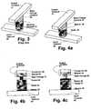
- FIG. 3shows a prior art 3-dimensional memory cell.
- FIG. 4 ashows a 3-dimensional memory cell usable with the present invention.
- FIGS. 4 b and 4 cshow alternatives to the memory cell of FIG. 4 a in which a narrow neck minimizes programming current.
- FIG. 5shows an array incorporating the memory cells of FIG. 4 a.
- FIG. 6shows a circuit diagram of memory cells usable with the present invention and programming levels applied according to the invention.
- FIG. 7shows set and reset pulses applied in conjunction with the present invention.
- FIG. 8shows a circuit for applying a selected pulse width and current to a selected cell for switching the cell between high and low resistance states.
- FIG. 8 ashows driver circuit 74 of FIG. 8 .
- FIG. 8 bshows detail of sense amplifier 76 of FIG. 8 .
- FIG. 9shows the circuit diagram of FIG. 6 with voltages for reading rather than programming.
- FIG. 10shows a portion of a 3-dimensional memory array further described in U.S. patent application Ser. No. 10/403,844, showing a useful word line layout.
- FIG. 11shows structures for controlling current and pulse width in the current mirror structure of FIG. 8 .
- FIG. 12shows other structures for controlling current and pulse width in the current mirror structure of FIG. 8 .
- phase change materialwill be used to describe a material that changes relatively easily from one stable state to another.
- the changeis typically from an amorphous state to a crystalline state or vice versa, but may include an intermediate change, such as from a more ordered crystalline state to an indeterminate state to an amorphous state, or vice versa.
- Phase change materialis converted from one state to the other by heating to high temperature, then cooling at a selected rate.
- Chalcogenidesare well-known phase change materials.
- phase change materialssuch as chalcogenides
- a nonvolatile memory cellin which a high-resistance, amorphous state represents one memory state while a low-resistance, crystalline state represents the other memory state, where memory states correspond to values of 1 and 0.
- FIG. 1shows a characteristic curve for a phase change material such as a chalcogenide.
- Two curvesrepresent the two states of the material.
- the materialWhen the material is in a low resistance state, as voltage is increased, the material follows the “set curve”, where a relatively straight line represents a relatively linear relationship between voltage and current. As voltage increases, current correspondingly increases, causing the material to move first through a “set current range” and then a “reset current range” to an indeterminate state labeled “X” in which the material does not exhibit either crystalline or amorphous properties.
- the materialwhen the material is in a high resistance state, the material follows the “reset curve”, where a voltage increase produces hardly any current until a snap back voltage, labeled V 3 , is reached.
- FIG. 2 ashows that with this rapid cooling, at a voltage labeled V 2 , current quickly decreases to a low level (as the amorphous state is entered) such that the material now exhibits a high resistance.
- FIG. 2 bshows movement along the reset curve of FIG. 1 .
- voltage applied to the memory cellproduces very little current until the voltage reaches a snap-back voltage V 3 , at which time voltage across the cell suddenly decreases and current suddenly increases until the set current range is reached.
- V 3a snap-back voltage
- the phase change materialis allowed to assume its indeterminate state and then voltage is decreased slowly, the material will follow the characteristic curve “to set state S” as the material cools and crystallizes into a low resistance state.
- Chalcogenidesare particularly useful examples of phase change materials, but it will be understood that other materials, such as silicon, which undergo appropriate and reliably detectable stable phase changes, can be used instead.
- FIG. 3shows a prior art nonvolatile memory cell in which a state change element 23 is placed in series with a steering element 22 , such as a diode. Although steering of the signal is assisted by steering element 22 , it is necessary to use high current to achieve state change of the entire state change element 23 .
- FIG. 4 ashows a memory cell further including a barrier layer 43 for concentrating current into a small area.
- Such heat concentrationis further described by Scheuerlein in concurrently filed U.S. application Ser. No._______, (attorney docket number MA-086-a-3) entitled “A Non-Volatile Memory Cell Comprising a Dielectric Layer and a Phase Change Material in Series”, which has been incorporated by reference herein.
- a voltageis applied across the dielectric or barrier layer 43 sufficient to cause dielectric breakdown across the dielectric layer, creating a low-resistance rupture region (or, in some cases, possibly more than one.)
- the diameter of such a rupture regionis very small.
- a typical rupture region formed by applying a voltage across a silicon dioxide layer about 2 to 3 nanometers thick sufficient to cause dielectric breakdownmay be tens of nanometers in diameter.
- Such a dielectric layer in which a low-resistance rupture region is formedis an example of an antifuse.
- An antifuseis characterized by the property of being insulating as formed, preventing current flow; then, when exposed to a high voltage, irreversibly changing its character to become conductive (at least in some regions) and allowing the flow of current.
- the very narrow rupture regionserves to focus the thermal energy into an extremely small volume, aiding conversion of phase change material in series with the dielectric layer having the rupture region.
- the dielectric layer having the rupture region and the phase change materialmay be formed in series, and interposed between conductors.
- Other elementsmay exist in the cell, such as a heater layer and a diode.
- the barrier layer in the cell of FIG. 4 amay be ruptured in a manufacturing environment by applying a high voltage to a selected cell, for example about eight volts in a 2.5 volt system, and grounding the word line. Unselected word lines may be held at about seven volts, and unselected bit lines may be held at about one volt during this rupture process. Preferred methods of rupturing the bits are described in more detail in U.S. patent application Ser. No. 10/403,844 filed by Scheuerlein on Mar. 31, 2003 entitled “Word Line Arrangement Having Multi-Layer Word Line Segments for Three-Dimensional Memory Array”, which is incorporated herein by reference.
- all memory cells to be used as addressable memorymay be ruptured in this manufacturing step to prepare the memory cells for user program operations.
- the rupture processmay leave the ruptured bits in the reset state or the set state.
- some bits on the chip, usually control bits,may be left not ruptured in this manufacturing step. These portions of the memory may then operate as antifuse memory cells instead of phase change memory cells.
- the states of these control bitsprovides permanent data bits useful for various purposes.
- antifuse memory cellsare useful to control the circuitry on the chip for trimming analog circuits, for imprinting manufacturing information, for setting redundancy address matching information, for bad bit pointer information, for setting a unique device identifier used for copyright protection control techniques, for altering the interface function of the device, for indicating to logic circuits on the chip that portions of the array are locked and the circuitry prevents any further programming of those portions, and for other customizable features of the device.
- rupturing these bitsrequires the use of test inputs that are not possible to activate or access after manufacturing is completed.
- the memory line drivers circuits, write circuits, and sense amplifier circuitsare shared between the two types of memory bits.
- the antifuse cellsare in a separate array with separate driver and read-write circuits.
- the circuitry of FIG. 6described in more detail below, may be used after manufacture to rupture the antifuse memory cells by increasing the bias levels to the higher voltage levels described above.
- the antifuse memory bitsare read using circuitry shown in FIG. 9 and described in further detail below.
- bottom conductor or input terminal 20is formed of a conductive material, for example a refractory metal or refractory metal compound such as tungsten or titanium tungsten.
- bottom conductor 20is in the form of a rail.
- barrier layer 43 of, for example, titanium nitridemay be used between diode 42 and state change element 23 .
- This memory cellcontacts an output terminal 21 in the form of a rail-shaped top conductor.
- Top conductor 21is preferably perpendicular to bottom conductor 20 .
- the rail shaped conductor 21is a multilayer structure including a layer of barrier material such as TiN and a layer of phase change material.
- the memory cell just describedincludes a non-ohmic conductive element, diode 42 , to serve as an isolation device.
- a non-ohmic conductive elementis characterized by a non-linear current vs. voltage curve.
- Other non-ohmic elementsmay be used in place of the diode.
- a metal-insulator-metal (MIM) deviceconsists of two metal (or metal-like) layers separated by a very thin insulator layer. When sufficient voltage is applied, charge carriers can tunnel across the insulator layer, but do not permanently damage it, as in an antifuse.
- the diode 42 of the memory cellcould be replaced with a MIM device.
- barrier layer 43phase change layer 23 , and diode layer 42 need not appear in the same orientation or order shown in FIG. 4 a.
- a barrier layer 19 of, for example, titanium nitridecan be located between input terminal 20 and diode 42 , and another barrier layer 24 can be adjacent conductor 25 as part of output terminal 21 .
- State change material 23can also be part of output terminal 21 and shaped as a rail.
- FIG. 4 bfurther shows a memory cell including a laterally etched reduced-area heater layer 44 for concentrating heat into a small area for faster heating with less current.
- Resistive heater element 44is formed from a resistive material such as titanium nitride.
- Such heat concentrationis further described by Scheuerlein in U.S. application Ser. No. ______, (attorney docket number MA-133 “A Non-Volatile Phase Change Memory Cell Having a Reduced Thermal Contact Area,” which has been incorporated by reference herein.
- Lateral etchingis used to form a reduced area of layer 44 .
- heatis concentrated near the small area of layer 44 and converts a small region of the phase change material 23 . With this heat concentration, less energy and less current are required to reach the “set range” and “reset range” of material 23 .
- Lateral etching of heater element 44may be achieved by changing the chemistry of etching materials to laterally etch the heater element material, as further explained by Scheuerlein in concurrently filed U.S. patent application Ser. No. ______ (attorney docket number MA-133).
- FIG. 4 cshows yet another alternative memory cell structure in which the state change material 23 rather than the heater material 44 has been narrowed for more efficient heating to achieve state change.
- a structuremay be achieved by forming a narrow post of sacrificial material, filling and planarizing around the narrow sacrificial post, and removing the sacrificial post to expose heater element 44 , and applying the state change material 23 , which then contacts heater element 44 in a narrow region.
- the structure of FIG. 4 cis also discussed in detail in the above mentioned patent application Ser. No. ______ (attorney docket number MA-133) incorporated herein by reference. See particularly the discussion of FIGS. 3 a -3 e of that application.
- the barrier layercan be above the phase change material rather than below, for example, or the diode can be above both the barrier layer, heater layer, and phase change layer.
- both the illustrated and reverse orders of layersare preferably used on different memory layers.
- FIG. 5shows an array incorporating memory cells 40 of the type shown in FIG. 4 a. It will be understood, however, that these details are not intended to be limiting, and that many of these details can be modified, omitted or augmented while the results still fall within the scope of the invention.
- FIG. 5shows a single memory level. Additional memory levels can be stacked, each monolithically formed above the one below it. Conductive lines in each memory level can be segmented or continuous, and two memory levels can share or not share a conductive line (input or output terminal).
- a layer or elementis considered to be in thermal contact with phase change material when thermal events within that layer or element are capable of thermally affecting the phase change material sufficient to cause it to detectably change phase.
- the biasing scheme of the present inventionguarantees that the voltage across unselected and half-selected cells is not sufficient to cause inadvertent conversion of those cells, and allows precise control of the power delivered to the cell to be programmed.
- the biasing schemealso minimizes leakage current through unselected and half-selected cells.
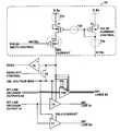
- FIG. 6shows a circuit representation, and may be a representation of an array such as shown in FIG. 5 .
- word linesare drawn horizontally and bit lines are drawn vertically.
- Memory cellsare drawn diagonally, and each is shown comprising a diode and a variable resistor.
- FIG. 6is drawn as a flat structure, a preferred structure may be a 3-dimensional structure in which word lines are in one layer, bit lines are in another layer, and memory cells are oriented vertically between the layers. It may be preferred to form bit lines and word lines on many layers above a semiconductor substrate to implement an integrated fully three-dimensional memory array. Any antifuse or other barrier material is not shown in FIG. 6 , but is preferably included.
- the diodes of memory cellshave their anodes in the direction of the bit lines and their cathodes in the direction of the word lines.
- a positive voltageis applied to the bit line of the selected memory cell, a negative (or ground) voltage is applied to the word line of the selected memory cell, a voltage close to the positive voltage is applied to unselected word lines, and a voltage close to the negative voltage or ground voltage is applied to unselected bit lines.
- This combinationapplies a strong positive voltage to the selected cell while applying small voltages to half selected cells and strong reverse bias to diodes of unselected memory cells.
- variable resistance phase change materialit is equally workable and equivalent to reverse bit lines and word lines, and to locate the variable resistance phase change material at the anodes rather than cathodes of the diodes.
- FIG. 6assumes it is desirable to write or read memory cell 1 , 2 , which is labeled “SELECTED”.
- Memory cell 1 , 2is connected between word line WORD 1 and bit line BIT 2 .
- SELECTEDMemory cell 1 , 2 is connected between word line WORD 1 and bit line BIT 2 .
- bit lines BIT 1 and BIT 3As a novel feature of the invention, by applying a positive voltage of 1.2 volts (for reading) or 2.5 volts (for writing) to bit line BIT 2 and applying ground voltage of 0 volts to word line WORD 1 while applying a voltage slightly higher than ground voltage to unselected bit lines (shown as bit lines BIT 1 and BIT 3 ) and applying a voltage, close to a write voltage, of 2 volts to unselected word lines (shown as word line WORD 2 ), it is possible to write or read memory cell 1 , 2 without any disturbance of unselected memory cells.
- unselected memory cell 2 , 3receives a back biased voltage of 2 volts minus 0.5 to 1 volt or a back bias of 0.5 to 1 volts, not enough to cause a breakdown of diode D 2 , 3 or excessive leakage current through these unselected cells.
- Half-selected memory cell 1 , 3(connected to selected word line WORD 1 but unselected bit line BIT 3 ) receives a forward bias of 0.5 to 1 volt, which, depending upon the manufacturing characteristics of diode D 1 , 3 and regardless of the current state of variable resistance R 1 , 3 , is less than the forward threshold of diode D 1 , 3 .
- Half-selected memory cell 2 , 2receives a bias to diode D 2 , 2 of 2.5 volts minus 2 volts, which is a forward bias of 0.5 volts.
- the forward biaswill be less than the threshold of the diode, which is easily achieved by simply selecting the voltages carefully.
- the threshold of a diodeis the voltage across the diode at which measurable current begins to flow, and below which current is negligible even when summing a thousand or more half-selected cells on a bit line or word line.
- This discussionhas used a 2.5-volt power supply, lower voltages may be preferred for smaller geometry memory cells. For example, voltages of 1.5 volts for WRITE and 0.75 volts for READ may be preferred for sub-100-nanometer technology. Also, higher voltages may be preferred for larger geometry memory cells.
- the biasing scheme of the present inventionproduces good isolation of unselected memory cells from the selected memory cell (or cells) and satisfactory isolation of half-selected memory cells. Since completely unselected memory cells (the majority in an array) are all back biased, leakage current through this large number of cells is minimized. Any forward biasing of half-selected memory cells will be below the diode turn-on threshold, and limited to one or a few selected bit lines or word lines. Therefore, even for memory cells in a low-resistance state, leakage will be negligible.
- bit line drivers D 1 , D 2 , and D 3select between the unselected voltage of 0.5 to 1 volt and the selected voltage of 2.5 volts, as controlled by decoder outputs.
- decoder output 2causes driver D 2 to select the 2.5 volt voltage while decoder outputs 1 and 3 cause drivers D 1 and D 3 to select the 0.5 to 1 volt voltage.
- word line decoder outputs 1 and 2cause word line driver W 1 to select the ground voltage GND and word line driver W 2 to select 2 volts. Structure for making these voltage selections is further described in connection with FIG. 5 of commonly owned U.S. patent application Ser. No. 10/306,887 filed Nov. 27, 2002 by Roy E. Scheuerlein, the subject matter of which is incorporated herein by reference.
- the chalcogenideTo convert a chalcogenide in a crystalline, low-resistance state to an amorphous, high-resistance state, the chalcogenide must be brought to a high temperature, for example about 700 degrees C., then allowed to cool quickly.
- the reverse conversion from an amorphous, high-resistance state to a crystalline, low-resistance stateis achieved by heating to a lower temperature, for example about 600 degrees C., then allowing the chalcogenide to cool relatively slowly.
- Circuit conditionsare carefully controlled in a monolithic three dimensional memory array formed according to a preferred embodiment of the present invention to avoid inadvertent conversion of the chalcogenide of neighboring cells during programming of a cell, or during repeated read events.
- Programming the cellmay change it from the first state to a second state (low to high resistance or high to low resistance).
- the cellcan subsequently be “erased”, returning it to the first state.
- FIG. 7shows shapes of pulses used to bring phase change material from one state to another.
- a logic 1For writing a logic 1 (set) into a memory cell, current is brought to an intermediate level (set pulse), and held at the intermediate level for a sufficient time for the crystalline structure of the phase change material to develop.
- set pulseFor one chalcogenide material that period of time is on the order of 500 to 1000 nanoseconds (0.5 to 1 microsecond). Current depends upon processing conditions and varies widely. In one embodiment, current through a single cell is about 20 microamps for setting (programming a logic 1) and about 100 microamps for resetting (programming a logic 0).
- reset pulseFor writing a logic 0 (reset) into a memory cell, current is brought to a higher level (reset pulse), then quickly removed, so that the reset pulse lasts on the order of 200 nanoseconds. This high current followed by rapid cooling puts the material into an amorphous state with high resistance.
- FIG. 8shows circuitry for programming and reading the memory array described in connection with FIG. 6 .
- FIG. 8illustrates a circuit 70 for controlling both pulse width and current used for writing to selected memory cells.
- a current mirror circuit 70includes a pulse width control transistor 73 as well as conventional current mirror transistors 71 and 72 .
- Circuit 70receives both a current control signal ICTRL in its master arm and a pulse width control signal WCTRL for controlling transistor 73 in series with its slave arm.
- a pulse width control transistoris located in series with the master arm, as indicated by 73 a.
- the pulse width control transistoris located between the master and slave arms as indicated by 73 b.
- the pulse width control transistormay be located between the slave current mirror device and the supply voltage connection, as indicated by 73 c.
- bit line decoderselects, from the many bit lines (typically over 1000), one or more bit lines on which memory cells are to be written. Typically, a WORD of 8 bits, or some other size, will be written at one time.
- bit line driver 74is selected by its bit line decoder output 91 to apply a WRITE voltage to bit line 81 .
- Bit line driver 74receives both an unselected bit line bias UBL and a selected bit line bias SBL.
- the selected bit line bias SBLis generated by current mirror circuit 70 .
- the bit line bias SBLis current controlled, not voltage controlled. Thus a precise current for a precise period of time is applied to the selected memory cell, bringing the selected memory cell to a desired temperature for a selected period and causing the selected value to be reliably written to the selected memory cell.
- FIG. 8 ashows an exemplary circuit for applying SBL and UBL.
- active low decoder output 91applies a high signal
- the unselected bit line bias voltage UBL BIASis applied by driver 74 or 74 B to bit line 81 or 82 through an NMOS device 89 so that when bit line 81 is not selected, bit line 81 moves to this UBL voltage.
- the SBL signal lineis selected by applying the low voltage to PMOS transistor 88 .
- control signal WCTRLturns on transistor 73
- the SBL signalis applied to the selected bit line 81 . More specifically, when pulse WCTRL is low, a current determined by pulse current control ICTRL is applied as the SBL current through transistor 73 to driver 74 and to bit line 81 .
- each current mirror slave device 71is associated with a single bit line, though master device 72 can be shared by several current mirror slave devices 71 .
- Two master devices 72one for the set current and one for the reset current, can control one or more slave devices 71 , by means of pass gates not shown, that interrupt the connection between each device 71 and the master device 72 .
- each current mirror slave device 71provides the desired current for setting or resetting its selected memory cell.
- bit line 81is to be programmed to a RESET state
- a RESET pulse as shown in FIG. 7is applied by circuit 70 and selected driver 74 to bit line 81 .
- the pulse width control circuitgenerates a short duration signal WCTRL about 200 ns long while the pulse current control signal ICTRL causes transistor 71 to carry a high current and thus heat the selected memory cell connected to bit line 81 to a high temperature quickly.
- WCTRLturns off transistor 73 after about 200 ns, the selected cell moves to an amorphous state with high resistance.
- a SET pulse as shown in FIG. 7is applied by circuit 70 and selected driver 74 to bit line 81 .
- WCTRLholds transistor 73 on for about 500 to 1000 ns while ICTRL causes transistor 71 to apply a relatively low current.
- the selected memory cellconverts to a low resistance crystalline state.
- bit line drivers 74 Bwill also receive this high SBL current, but will not be activated by their bit line decoder outputs, and thus will not apply the selected bit line current SBL CURRENT to their respective bit lines, but will continue to apply the unselected bit line bias voltage UBL BIAS to their bit lines. Therefore these unselected bit lines will not be programmed by current mirror circuit 70 .
- driver 77will also receive the same bit line decoder output 91 as a control input. But these other bit line drivers each receive a separate SBL CURRENT from a corresponding current mirror circuit 70 , as represented in FIG. 8 by SBL 2 CURRENT. Thus driver 77 illustrates one of several additional drivers for driving different bit lines in response to a single decoder signal for simultaneously writing a multi-bit word.
- cell 1 , 2has been selected by bringing low word line WORD 1 while bringing bit line BIT 2 high.
- Other bit linesare at 0.5 to 1 volts and other word lines are at 2 volts, which reverse biases all unselected cells such as cell 2 , 3 .
- Half-selected cellssuch as cell 1 , 1 and cell 1 , 3 connected to selected word line WORD 1 and half-selected cells such as cell 2 , 2 connected to bit line BIT 2 receive a forward bias of about 0.5 to 1 volt, not enough to cause writing to these half-selected cells.
- next WRITE operationis to cell 2 , 3 and bit line BIT 3 is brought to 2.5 volts before word line WORD 1 has returned to its unselected value of 2 volts
- cell 1 , 3may be erroneously written.
- a deselect control device 75connects a previously connected signal line to the unselected voltage UBL.
- pulse width control signal WCTRLhas deactivated its pulse through transistor 73
- deselect control signal 75goes high, and causes the unselected bias voltage UBL to be applied to the respective bit line, for example bit line 81 illustrated in FIG. 8 .
- bit line 81illustrated in FIG. 8 .
- bit line decoder outputs 92causes a corresponding one of bit line drivers 74 B to connect the SBL CURRENT node to the corresponding one of bit lines 82 .
- the selected one of bit lines 82will be at a voltage close to UBL and will remain at this voltage until the next pulse control signal WCTRL applies current selected by ICTRL to this new bit line 82 (current will be determined by ICTRL depending on whether the new memory cell is to be SET or RESET).
- the selected word lineis pulled to its selected low level
- the selected bit lineseach receive their selected currents for a selected pulse width, depending on the value to be written;
- the selected word line voltagesare returned to their unselected higher levels.
- bit lines connected to a group of bit line driverssuch as driver 77 controlled by the same bit line decoder output 91 are not all selected for writing.
- Some of the groupare connected to a circuit 70 with device 73 turned off and their associated deselect control device 75 turned on during the write pulse time for other bits lines in the group.
- the number of bit line drivers connected to a bit line decoder outputcan be larger than the number of selected bit lines. For example 16 bit lines can be controlled by a single decoder, but only 8 of the 16 are selected bit lines.
- the decodercan be constructed with a width equal to the width taken up by 16 bit lines rather than just 8 selected bit lines.
- bit lines in the group that are controlled by the same decoderreceive one of three conditions from their respective SBL CURRENT nodes.
- the three conditionsinclude 1) a set current, 2) a reset current or 3) for those bit lines not selected, an unselected bit line bias.
- the bit line drivers in the grouppass any of these three conditions to their associated bit lines through device 88 of FIG. 8 a. Similarly, not all bit lines in the group are necessarily selected for reading at the same time.
- diodesare reversed in orientation, and voltage levels are correspondingly reversed.
- the important factorsare to return selected lines to their unselected levels so that all diodes become reverse biased before initiating a next read or write operation. Note that when all cells are unselected, all diodes are reverse biased, thus minimizing leakage, and minimizing the chance that any cells will be erroneously disturbed.
- FIG. 8illustrates circuitry for applying current to selected bit lines
- circuitryis also provided for bringing word line voltages to selected levels.
- selected levelsare low rather than high
- an n-channel transistorsprovides a selected word line bias.
- a circuit for driving array lines and appropriate for driving word lines in the present inventionhas been illustrated by Roy E. Scheuerlein and Matthew P. Crowley in co-pending Patent Application Publication No. US 2003/0214841 entitled “MULTI-HEADED DECODER STRUCTURE UTILIZING MEMORY ARRAY LINE DRIVER WITH DUAL PURPOSE DRIVER DEVICE”, filed Nov. 27, 2002 and incorporated herein by reference. See, for example, FIG. 3 of that application and its discussion.
- the selected word lineis brought to a low voltage for a time longer than any of the bit line pulses for writing logic 0 (a short high current pulse to the bit line) and logic 1 (a longer lower current pulse to the bit line, see FIG. 7 ) are applied.
- the word linesare preferably low resistance lines so that several bits on a word line can be written simultaneously without a voltage swing to the word line that would disturb writing to any of the cells.
- the word lineis much shorter than a bit line, in one embodiment, about one eighth the length of a bit line.
- FIG. 9shows such voltages applied to the memory cell array for reading memory cells. As shown in FIG. 9 , a voltage of 1.2 volts is applied to unselected word lines such as WORD 2 and also to the selected bit line BIT 2 .
- Operational amplifierssuch as 76 shown in FIG. 8 (also 8 b ) detect current through the cell or cells selected for reading. (To assist understanding of the relationship between FIG. 8 and FIG. 9 , FIG. 9 includes current mirror structure 70 and operational amplifier 76 also shown in FIG. 8 .)
- FIG. 8 bshows detail of the operational amplifier 76 of FIG. 8 .
- operational amplifier 85maintains the SBL BIAS on the minus input of operational amplifier 85 at the level of VREF, which in this example is 1.2 volts.
- feedback resistor 86connects the READ output voltage to the SBL bias line (which is in turn connected through a driver and bit line to a selected cell), READ current through resistor 86 is substantially equal to current through the selected cell, and therefore indicates the state of the selected cell.
- the two terminals of the half-selected cellsmay be brought to the same voltage.
- One simple way to accomplish thisis to connect the positive input terminals of operational amplifiers 85 to the voltage supply of unselected word lines. Then operational amplifiers 85 will use feedback resistors 86 to bring the selected bit lines and unselected word lines to the same voltage.
- the group of cells comprising a single wordmay be located in a vertical stack, and a word line may include segments physically extending through many memory layers connected by vertically oriented vias (sometimes called zias because of their orientation in the z direction).
- the memorymay be arranged such that a plurality of memory cells to be programmed together are connected to a single word line and may be on different layers of memory cells although they are to be programmed in response to a single address.
- a word line segmentmay be shared by memory cells located in memory layers both above and below the word line, thereby reducing the number of word line segments and reducing manufacturing complexity. Bit lines may also be shared by memory cells both above and below.
- FIG. 10shows a portion of a three-dimensional memory array, showing a useful word line layout.
- a word line WLaccesses 16 memory cells arranged in a 4 by 4 array on four different memory cell layers within the 3-dimensional integrated circuit memory array. Sixteen bit lines BL 1 , 1 through BL 4 , 4 extend through this 4 by 4 array of memory cells.
- Additional memory cellssuch as shown in FIG. 10 are located in front of or behind the sixteen memory cells and bit line portions shown, and are connected to different word lines not shown.
- the sixteen memory cells shown in FIG. 10may be considered to be a single word, and a memory WRITE instruction may refer to all sixteen of the memory cells.
- a single current mirror structuresuch as structure 70 of FIG. 8 may supply the current to sequentially write to, for example, the four memory cells M 1 , 1 through M 4 , 1 .
- a first plurality of memory cells M 1 , 1 through M 1 , 4may be written simultaneously as controlled by four current mirror structures 70 .
- bit lines BL 1 , 1 through BL 1 , 4are brought to their unselected levels (see above discussion of deselection control transistor 75 of FIG. 8 ) and bit lines BL 2 , 1 through BL 2 , 4 are selected by their respective bit line drivers (for example one of drivers 74 B in FIG. 8 ) to receive controlled current and pulse width for writing selected values into memory cells M 2 , 1 through M 2 , 4 . Subsequently, while word line WL is still selected, the third and fourth columns of memory cells connected to word line WL are written.
- control currents ICTRLto current mirrors 70 that will drive one of the columns in FIG. 10 before the new bit lines are selected and write pulses WCTRL are activated, and while previous bit lines are being brought to their unselected voltage levels by turning on respective transistors 75 .
- FIG. 11illustrates circuits for providing a selected pulse width WCTRL and a selected current ICTRL to the current mirror 70 of FIG. 8 .
- Pulse width selector circuit 110includes a string of inverters 1 through 7 , with a length selected by pulse width select multiplexer 8 .
- OR gate 9is a one-shot device that provides a low output signal only when its two input signals are both low. But the input signals are only both low when a low signal has been provided by the PULSE CLOCK input signal and has not yet propagated to OR gate 9 through the string of inverters. Thus the low pulse occurs during this propagation time.
- Multiplexer 8allows for two different pulse widths, causing a short pulse width when the PULSE CLOCK signal propagates only through inverters 1 - 3 and a longer pulse when the signal propagates through all seven inverters 1 - 7 .
- the pulse lengthscan be precisely determined during manufacture by selecting the size and composition of the inverters.
- Current select circuit 120selects between two currents to be applied as ICTRL to current mirror 70 .
- a current generator control signal IGENcontrols transistors 121 through 125 .
- Transistor 121is the master arm for a current mirror in which the slave is either transistor 122 or the combination of transistors 123 through 125 .
- one transistor 122provides the set control current ICTRLSet through multiplexer 126 as the ICTRL current to pulse control transistor 72 in the master arm of current mirror 70 , while three transistors 123 through 125 are connected in parallel to multiplexer 126 to provide the reset current signal ICTRLReset. Therefore ICTRLReset is higher and will cause the slave arm of current mirror 70 to in turn provide a higher reset current as the SBL CURRENT (see also FIG. 8 ).
- Multiplexer 126selects between its two input currents as controlled by the WRITE SELECT control signal. The output of multiplexer 126 in combination with the WCTRL signal determines whether the SBL CURRENT will cause a set (logic 1) or reset (logic 0) to be written to the selected memory cell.
- FIG. 12shows another such circuit.
- current mirror 70is replaced by a current mirror 170 having no pulse width control transistor.
- Pulse controlis provided by a different pulse width generator circuit 130 having parallel OR gates 11 and 12 providing pulses from inverter strings of different lengths and a different current select circuit 140 .
- the PULSE WIDTH SELECT signalcauses one of transistors 14 and 15 to turn on, providing either a SET pulse width signal WCTRLSet to transistor 73 e for a low longer ICTRLSet current when a memory cell is to be set, or a RESET pulse width signal WCTRLReset to transistor 73 f for a high short ICTRLReset current when a memory cell is to be reset.
- unselected bias voltagesare provided, one for each bit line layer of each memory sub-array.
- unselected bit lines on each layermay be biased independently of unselected bit lines on other layers, the implementation of which is described more fully in connection with FIGS. 8, 9, and 10 of U.S. Pat. No. 6,735,104, entitled “Memory Device with Row and Column Decoder Circuits Arranged in a Checkerboard Pattern Under a Plurality of Memory Arrays”, by Roy E. Scheuerlein, which is incorporated herein by reference.
- unselected bias node voltagesmay be advantageously generated by a group of four unselected bias generator circuits, one associated with each layer.
- Each such unselected bias generator circuitreceives address signals which are used to decode the selected memory plane (i.e., the selected array line layer) to generate bias voltages or conditions appropriately. Furthermore, in a programmable device, additional signals may be received which communicate the mode of operation to the unselected bias generator circuits. For example, the unselected bit line bias voltage may likely be different for read mode than for write mode, and the multi-headed decoder circuits described above may be effectively used in either mode of operation if the decoder provides a decoded output 91 having suitable voltage levels.
- memory line driversare arranged on opposite sides of the memory array and control alternate memory lines. Since the drivers and not the memory line width control memory line pitch, the memory line pitch can be twice as small as would be allowed by the layout of the memory line driver. Such a layout is illustrated in FIG. 4 of the above referenced U.S. Pat. No. 6,735,104.
- each array line driver circuiti.e., array line decoder “head” preferably includes two transistors, as described herein in connection with FIG. 8 a. Nonetheless, other configurations are contemplated for the heads. For example, N-channel transistors may be exclusively used if the various bias conditions lend themselves to such use. Moreover, additional transistors may be employed to accomplish additional functions if layout area permits. While three-dimensional arrays have been discussed in detail, multi-headed decoder circuits are also useful in memory arrays having only one plane of memory cells, although the layout density advantages of multi-headed decoders are more beneficial in three-dimensional arrays having more than one memory plane.
- Word linesmay also be referred to as row lines or X-lines, and bit lines may also be referred to as column lines or Y-lines.
- word linesmay carry at least two different connotations to those skilled in the art.
- word linesare held at a selected bias level and bit lines are sensed.
- X-linesor word lines
- Y-linesor bit lines
- the memory organizationmay suggest one set of the two array lines is more aligned with data “bits” rather than data “words.”
- word lines and bit linesrepresent orthogonal array lines, and has followed the common assumption in the art that word lines are driven and bit lines are sensed. But the benefits of the invention can be applied either way.
- a memory arraymay be a two dimensional (planar) memory array having a memory level formed in a substrate, or alternatively formed above the substrate.
- the substratemay either be a monocrystalline substrate, such as might include support circuitry for the memory array, or may be another type of substrate, which need not necessarily include support circuitry for the memory array.
- certain embodiments of the inventionmay be implemented utilizing a silicon-on-insulator (SOI) structure, and others utilizing a silicon-on-sapphire (SOS) structure.
- SOIsilicon-on-insulator
- SOSsilicon-on-sapphire
- a memory arraymay be the above-discussed three-dimensional array having more than one plane of memory cells.
- the memory planesmay be formed above a substrate including support circuitry for the memory array.
- an integrated circuit having a three-dimensional memory arrayis assumed to be a monolithic integrated circuit, rather than an assembly of more than one monolithic integrated circuit packaged together or in close proximity, or die-bonded together.
- Integrated circuits incorporating a memory arrayusually subdivide the array into a sometimes large number of smaller arrays, also sometimes known as sub-arrays.
- an arrayis a contiguous group of memory cells having contiguous word and bit lines generally unbroken by decoders, drivers, sense amplifiers, and input/output circuits.
- An integrated circuit including a memory arraymay have one array, more than one array, or even a large number of arrays.
- U.S. patent application Ser. No. ______(attorney docket number MA-134), concurrently filed herewith and incorporated herein by reference, describes memory levels not all having the same type of memory cell, and describes memory levels having cells of one type alternating with memory levels using other types of memory cells.
- a useful memory array structureincludes memory cells having a phase change element, an antifuse, and a diode, so that any memory cell can be used for either storing frequently re-written data or storing the control information.
- circuits and physical structuresare generally presumed, it is well recognized that in modern semiconductor design and fabrication, physical structures and circuits may be embodied in computer readable descriptive form suitable for use in subsequent design, test or fabrication stages as well as in resultant fabricated semiconductor integrated circuits. Accordingly, claims directed to traditional circuits or structures may, consistent with particular language thereof, read upon computer readable encodings and representations of same, whether embodied in media or combined with suitable reader facilities to allow fabrication, test, or design refinement of the corresponding circuits and/or structures.
- the inventionis contemplated to include circuits, related methods or operation, related methods for making such circuits, and computer-readable medium encodings of such circuits and methods, all as described herein, and as defined in the appended claims.
- a computer-readable mediumincludes at least disk, tape, or other magnetic, optical, semiconductor (e.g., flash memory cards, ROM), or electronic medium and a network, wireline, wireless or other communications medium.
- An encoding of a circuitmay include circuit schematic information, physical layout information, behavioral simulation information, and/or may include any other encoding from which the circuit may be represented or communicated.
Landscapes
- Engineering & Computer Science (AREA)
- Chemical & Material Sciences (AREA)
- Crystallography & Structural Chemistry (AREA)
- Computer Hardware Design (AREA)
- Power Engineering (AREA)
- Semiconductor Memories (AREA)
- Static Random-Access Memory (AREA)
Abstract
Description
- This application relates to Herner et al., U.S. patent application Ser. No. 10/855,784, “An Improved Method for Making High-Density Nonvolatile Memory,” filed May 26, 2004; which is a continuation of Herner et al., U.S. patent application Ser. No. 10/326,470, “An Improved Method for Making High-Density Nonvolatile Memory,” filed Dec. 19, 2002 (since abandoned) and hereinafter the '470 application, both assigned to the assignee of the present invention and hereby incorporated by reference in their entirety.
- This application also relates to Scheuerlein et al, U.S. application Ser. No. ______, (attorney docket number MA-086-a-3) entitled “A Non-Volatile Memory Cell Comprising a Dielectric Layer and a Phase Change Material in Series”; to Scheuerlein, U.S. application Ser. No. ______, (attorney docket number MA-133) entitled “A Non-Volatile Phase Change Memory Cell Having a Reduced Thermal Contact Area”; and to Scheuerlein, U.S. application Ser. No.______, (attorney docket number MA-134) entitled “A Write-Once Nonvolatile Phase Change Memory Array”; all filed herewith and incorporated herein by reference.
- The invention relates to programming and reading a nonvolatile memory cell comprising a dielectric and/or diode and a phase-change element in series.
- Phase-change materials such as chalcogenides have been used in nonvolatile memories. Such materials can exist in one of two or more stable states, usually high-resistance and low-resistance states. In chalcogenides, the high-resistance state corresponds to an amorphous state, while the low-resistance state corresponds to a more ordered crystalline state. The conversion between states is generally achieved thermally.
- Integrated circuit memories are typically large arrays of memory cells connected between bit lines and word lines. In order to achieve reliable programming and reading of the memory cells within the array, memory cells selected to be programmed or read must be isolated from memory cells that are not selected. It sometimes occurs that cells adjacent to selected cells are disturbed during a write operation, or that cells on the same word line or bit line as selected cells may be disturbed during the write operation. This problem becomes increasingly important as operating voltages are decreased, write speeds are increased, memory cell densities are increased, and array sizes are increased.
- There is a need for improved methods of programming and reprogramming the memory cells. The cells must be programmed quickly, using low current, and in a manner that assures proper writing and reading of memory cells in the array. One problem when writing and reading memories is that switching occurs very fast, and sometimes a word line or bit line that was recently selected may not have returned to its resting voltage when the next word line or bit line is selected, and selecting a new word line or bit line may cause unintentional programming (or reading) of a cell connected to a previously selected word line or bit line.
- The present invention is defined by the appended claims, and nothing in this section should be taken as a limitation on those claims. In general, the invention is directed to methods of programming an array of nonvolatile memory cells each comprising a phase change element in series with a diode. The invention takes advantage of the one-way nature of the diode and applies biasing voltages that minimize leakage current through unselected cells. The invention preferably follows a preferred order for biasing word lines and bit lines to decrease the likelihood of programming or reading an unselected cell.
FIG. 1 is a characteristic curve for a two-state memory element such as a chalcogenide.FIGS. 2 aand2bshow movement between set and reset states for the memory element ofFIG. 1 .FIG. 3 shows a prior art 3-dimensional memory cell.FIG. 4 ashows a 3-dimensional memory cell usable with the present invention.FIGS. 4 band4cshow alternatives to the memory cell ofFIG. 4 ain which a narrow neck minimizes programming current.FIG. 5 shows an array incorporating the memory cells ofFIG. 4 a.FIG. 6 shows a circuit diagram of memory cells usable with the present invention and programming levels applied according to the invention.FIG. 7 shows set and reset pulses applied in conjunction with the present invention.FIG. 8 shows a circuit for applying a selected pulse width and current to a selected cell for switching the cell between high and low resistance states.FIG. 8 ashows driver circuit 74 ofFIG. 8 .FIG. 8 bshows detail ofsense amplifier 76 ofFIG. 8 .FIG. 9 shows the circuit diagram ofFIG. 6 with voltages for reading rather than programming.FIG. 10 shows a portion of a 3-dimensional memory array further described in U.S. patent application Ser. No. 10/403,844, showing a useful word line layout.FIG. 11 shows structures for controlling current and pulse width in the current mirror structure ofFIG. 8 .FIG. 12 shows other structures for controlling current and pulse width in the current mirror structure ofFIG. 8 .- While many solid materials can change between crystalline and amorphous states, in this discussion the term “phase change material” will be used to describe a material that changes relatively easily from one stable state to another. The change is typically from an amorphous state to a crystalline state or vice versa, but may include an intermediate change, such as from a more ordered crystalline state to an indeterminate state to an amorphous state, or vice versa. Phase change material is converted from one state to the other by heating to high temperature, then cooling at a selected rate. Chalcogenides are well-known phase change materials.
- It is known to use phase change materials, such as chalcogenides, in a nonvolatile memory cell, in which a high-resistance, amorphous state represents one memory state while a low-resistance, crystalline state represents the other memory state, where memory states correspond to values of 1 and 0. (If intermediate stable states are achieved, more than two memory states can exist for each cell; for simplicity, the examples in this discussion will describe only two memory states.)
FIG. 1 shows a characteristic curve for a phase change material such as a chalcogenide. Two curves represent the two states of the material. When the material is in a low resistance state, as voltage is increased, the material follows the “set curve”, where a relatively straight line represents a relatively linear relationship between voltage and current. As voltage increases, current correspondingly increases, causing the material to move first through a “set current range” and then a “reset current range” to an indeterminate state labeled “X” in which the material does not exhibit either crystalline or amorphous properties. Alternatively, when the material is in a high resistance state, the material follows the “reset curve”, where a voltage increase produces hardly any current until a snap back voltage, labeled V3, is reached. At that point, resistance quickly decreases and the current moves into the “set range”. It can be seen that as current increases, the “reset curve” moves closer to the “set curve”. Maintaining the current in the “set range” for a sufficient period of time for the material to change to its crystalline state causes the material to converge to the “set curve”. Subsequently when the current is reduced from the “set range” the materials cools slowly and the material stays in the set state. In a future programming operation, increasing voltage then causes the material to follow the set curve through the set current range to the reset current range where the two curves coincide at the indeterminate state X. From indeterminate state X, a rapid decrease in voltage and current causes the material to quickly cool and solidify into an amorphous state.FIG. 2 ashows that with this rapid cooling, at a voltage labeled V2, current quickly decreases to a low level (as the amorphous state is entered) such that the material now exhibits a high resistance.FIG. 2 bshows movement along the reset curve ofFIG. 1 . Starting in the high resistance reset state R, voltage applied to the memory cell produces very little current until the voltage reaches a snap-back voltage V3, at which time voltage across the cell suddenly decreases and current suddenly increases until the set current range is reached. At this point, if the phase change material is allowed to assume its indeterminate state and then voltage is decreased slowly, the material will follow the characteristic curve “to set state S” as the material cools and crystallizes into a low resistance state.- Chalcogenides are particularly useful examples of phase change materials, but it will be understood that other materials, such as silicon, which undergo appropriate and reliably detectable stable phase changes, can be used instead.
FIG. 3 shows a prior art nonvolatile memory cell in which astate change element 23 is placed in series with asteering element 22, such as a diode. Although steering of the signal is assisted by steeringelement 22, it is necessary to use high current to achieve state change of the entirestate change element 23.- To facilitate conversion, mechanisms have been used to concentrate heat in a relatively small area contacting the phase change material.
FIG. 4 ashows a memory cell further including abarrier layer 43 for concentrating current into a small area. Such heat concentration is further described by Scheuerlein in concurrently filed U.S. application Ser. No.______, (attorney docket number MA-086-a-3) entitled “A Non-Volatile Memory Cell Comprising a Dielectric Layer and a Phase Change Material in Series”, which has been incorporated by reference herein. - A voltage is applied across the dielectric or
barrier layer 43 sufficient to cause dielectric breakdown across the dielectric layer, creating a low-resistance rupture region (or, in some cases, possibly more than one.) The diameter of such a rupture region is very small. A typical rupture region formed by applying a voltage across a silicon dioxide layer about 2 to 3 nanometers thick sufficient to cause dielectric breakdown may be tens of nanometers in diameter. - Such a dielectric layer in which a low-resistance rupture region is formed is an example of an antifuse. An antifuse is characterized by the property of being insulating as formed, preventing current flow; then, when exposed to a high voltage, irreversibly changing its character to become conductive (at least in some regions) and allowing the flow of current.
- The very narrow rupture region serves to focus the thermal energy into an extremely small volume, aiding conversion of phase change material in series with the dielectric layer having the rupture region. For example, the dielectric layer having the rupture region and the phase change material may be formed in series, and interposed between conductors. Other elements may exist in the cell, such as a heater layer and a diode.
- The barrier layer in the cell of
FIG. 4 amay be ruptured in a manufacturing environment by applying a high voltage to a selected cell, for example about eight volts in a 2.5 volt system, and grounding the word line. Unselected word lines may be held at about seven volts, and unselected bit lines may be held at about one volt during this rupture process. Preferred methods of rupturing the bits are described in more detail in U.S. patent application Ser. No. 10/403,844 filed by Scheuerlein on Mar. 31, 2003 entitled “Word Line Arrangement Having Multi-Layer Word Line Segments for Three-Dimensional Memory Array”, which is incorporated herein by reference. - In some embodiments, all memory cells to be used as addressable memory may be ruptured in this manufacturing step to prepare the memory cells for user program operations. The rupture process may leave the ruptured bits in the reset state or the set state. However, some bits on the chip, usually control bits, may be left not ruptured in this manufacturing step. These portions of the memory may then operate as antifuse memory cells instead of phase change memory cells. The states of these control bits provides permanent data bits useful for various purposes. These antifuse memory cells are useful to control the circuitry on the chip for trimming analog circuits, for imprinting manufacturing information, for setting redundancy address matching information, for bad bit pointer information, for setting a unique device identifier used for copyright protection control techniques, for altering the interface function of the device, for indicating to logic circuits on the chip that portions of the array are locked and the circuitry prevents any further programming of those portions, and for other customizable features of the device. In one embodiment, rupturing these bits requires the use of test inputs that are not possible to activate or access after manufacturing is completed. In one embodiment, the memory line drivers circuits, write circuits, and sense amplifier circuits are shared between the two types of memory bits. In another embodiment, the antifuse cells are in a separate array with separate driver and read-write circuits. In either case the circuitry of
FIG. 6 , described in more detail below, may be used after manufacture to rupture the antifuse memory cells by increasing the bias levels to the higher voltage levels described above. The antifuse memory bits are read using circuitry shown inFIG. 9 and described in further detail below. - Referring to
FIG. 4 a,bottom conductor orinput terminal 20 is formed of a conductive material, for example a refractory metal or refractory metal compound such as tungsten or titanium tungsten. In this exemplary cell,bottom conductor 20 is in the form of a rail. As shown inFIG. 4 a,barrier layer 43 of, for example, titanium nitride may be used betweendiode 42 andstate change element 23. This memory cell contacts anoutput terminal 21 in the form of a rail-shaped top conductor.Top conductor 21 is preferably perpendicular tobottom conductor 20. In one embodiment shown in FIG. 2 of concurrently filed U.S. application Ser. No._____, (attorney docket number MA-086-a-3) entitled “A Non-Volatile Memory Cell Comprising a Dielectric Layer and a Phase Change Material in Series” (incorporated herein by reference), the rail shapedconductor 21 is a multilayer structure including a layer of barrier material such as TiN and a layer of phase change material. - The cells just described are just a few examples of the forms that a nonvolatile memory cell formed according to the present invention may take; clearly many other configurations are possible. For example, the memory cell just described includes a non-ohmic conductive element,
diode 42, to serve as an isolation device. A non-ohmic conductive element is characterized by a non-linear current vs. voltage curve. Other non-ohmic elements may be used in place of the diode. For example, a metal-insulator-metal (MIM) device consists of two metal (or metal-like) layers separated by a very thin insulator layer. When sufficient voltage is applied, charge carriers can tunnel across the insulator layer, but do not permanently damage it, as in an antifuse. In alternative embodiments of the present invention, thediode 42 of the memory cell could be replaced with a MIM device. - It will be understood, of course, that many variations on the cell of
FIG. 4 aare possible. Thebarrier layer 43,phase change layer 23, anddiode layer 42 need not appear in the same orientation or order shown inFIG. 4 a.As shown inFIG. 4 b,abarrier layer 19 of, for example, titanium nitride can be located betweeninput terminal 20 anddiode 42, and another barrier layer24 can beadjacent conductor 25 as part ofoutput terminal 21.State change material 23 can also be part ofoutput terminal 21 and shaped as a rail. FIG. 4 bfurther shows a memory cell including a laterally etched reduced-area heater layer 44 for concentrating heat into a small area for faster heating with less current.Resistive heater element 44 is formed from a resistive material such as titanium nitride. Such heat concentration is further described by Scheuerlein in U.S. application Ser. No. ______, (attorney docket number MA-133 “A Non-Volatile Phase Change Memory Cell Having a Reduced Thermal Contact Area,” which has been incorporated by reference herein. Lateral etching is used to form a reduced area oflayer 44. When current flows through the memory cell, heat is concentrated near the small area oflayer 44 and converts a small region of thephase change material 23. With this heat concentration, less energy and less current are required to reach the “set range” and “reset range” ofmaterial 23.- Lateral etching of
heater element 44 may be achieved by changing the chemistry of etching materials to laterally etch the heater element material, as further explained by Scheuerlein in concurrently filed U.S. patent application Ser. No. ______ (attorney docket number MA-133). FIG. 4 cshows yet another alternative memory cell structure in which thestate change material 23 rather than theheater material 44 has been narrowed for more efficient heating to achieve state change. Such a structure may be achieved by forming a narrow post of sacrificial material, filling and planarizing around the narrow sacrificial post, and removing the sacrificial post to exposeheater element 44, and applying thestate change material 23, which thencontacts heater element 44 in a narrow region. The structure ofFIG. 4 cis also discussed in detail in the above mentioned patent application Ser. No. ______ (attorney docket number MA-133) incorporated herein by reference. See particularly the discussion of FIGS. 3a-3eof that application.- The barrier layer can be above the phase change material rather than below, for example, or the diode can be above both the barrier layer, heater layer, and phase change layer. In some three-dimensional embodiments with multiple layers of memory cells, both the illustrated and reverse orders of layers are preferably used on different memory layers.
FIG. 5 shows an array incorporatingmemory cells 40 of the type shown inFIG. 4 a.It will be understood, however, that these details are not intended to be limiting, and that many of these details can be modified, omitted or augmented while the results still fall within the scope of the invention.FIG. 5 shows a single memory level. Additional memory levels can be stacked, each monolithically formed above the one below it. Conductive lines in each memory level can be segmented or continuous, and two memory levels can share or not share a conductive line (input or output terminal).- The photolithography techniques described in Chen, U.S. application Ser. No. 10/728,436, “Photomask Features with Interior Nonprinting Window Using Alternating Phase Shifting,” filed Dec. 5, 2003; or Chen, U.S. application Ser. No. 10/815,312, “Photomask Features with Chromeless Nonprinting Phase Shifting Window,” filed Apr. 1, 2004, both owned by the assignee of the present invention and hereby incorporated by reference, can advantageously be used to perform any photolithography step used in formation of a memory array according to the present invention.
- While the structure of the array just described diverges in some important ways from the structure of the array of Herner et al., wherever they are the same, the fabrication methods of Herner et al. can be used. For clarity, not all of the fabrication details of Herner et al. were included in this description, but no part of that description is intended to be excluded.
- A layer or element is considered to be in thermal contact with phase change material when thermal events within that layer or element are capable of thermally affecting the phase change material sufficient to cause it to detectably change phase. In some embodiments, it is preferred to place antifuse or heater layers in thermal contact with the phase change material to assist with phase change heating.
- Circuitry and Programming
- The biasing scheme of the present invention guarantees that the voltage across unselected and half-selected cells is not sufficient to cause inadvertent conversion of those cells, and allows precise control of the power delivered to the cell to be programmed. The biasing scheme also minimizes leakage current through unselected and half-selected cells.
FIG. 6 shows a circuit representation, and may be a representation of an array such as shown inFIG. 5 . InFIG. 6 , word lines are drawn horizontally and bit lines are drawn vertically. Memory cells are drawn diagonally, and each is shown comprising a diode and a variable resistor. Thus, even thoughFIG. 6 is drawn as a flat structure, a preferred structure may be a 3-dimensional structure in which word lines are in one layer, bit lines are in another layer, and memory cells are oriented vertically between the layers. It may be preferred to form bit lines and word lines on many layers above a semiconductor substrate to implement an integrated fully three-dimensional memory array. Any antifuse or other barrier material is not shown inFIG. 6 , but is preferably included.- In
FIG. 6 , the diodes of memory cells have their anodes in the direction of the bit lines and their cathodes in the direction of the word lines. A positive voltage is applied to the bit line of the selected memory cell, a negative (or ground) voltage is applied to the word line of the selected memory cell, a voltage close to the positive voltage is applied to unselected word lines, and a voltage close to the negative voltage or ground voltage is applied to unselected bit lines. This combination applies a strong positive voltage to the selected cell while applying small voltages to half selected cells and strong reverse bias to diodes of unselected memory cells. - It is equally workable and equivalent to reverse bit lines and word lines, and to locate the variable resistance phase change material at the anodes rather than cathodes of the diodes.
- The particular illustration of
FIG. 6 assumes it is desirable to write or readmemory cell Memory cell memory cell memory cell memory cell memory cell 1,3 (connected to selected word line WORD1 but unselected bit line BIT3) receives a forward bias of 0.5 to 1 volt, which, depending upon the manufacturing characteristics of diode D1,3 and regardless of the current state of variable resistance R1,3, is less than the forward threshold of diode D1,3. Half-selectedmemory cell - Thus, it can be seen that the biasing scheme of the present invention produces good isolation of unselected memory cells from the selected memory cell (or cells) and satisfactory isolation of half-selected memory cells. Since completely unselected memory cells (the majority in an array) are all back biased, leakage current through this large number of cells is minimized. Any forward biasing of half-selected memory cells will be below the diode turn-on threshold, and limited to one or a few selected bit lines or word lines. Therefore, even for memory cells in a low-resistance state, leakage will be negligible.
- To apply respective programming voltages, bit line drivers D1, D2, and D3 (and many more not shown) select between the unselected voltage of 0.5 to 1 volt and the selected voltage of 2.5 volts, as controlled by decoder outputs. In
FIG. 6 ,decoder output 2 causes driver D2 to select the 2.5 volt voltage whiledecoder outputs line decoder outputs - Programming
- To convert a chalcogenide in a crystalline, low-resistance state to an amorphous, high-resistance state, the chalcogenide must be brought to a high temperature, for example about 700 degrees C., then allowed to cool quickly. The reverse conversion from an amorphous, high-resistance state to a crystalline, low-resistance state is achieved by heating to a lower temperature, for example about600 degrees C., then allowing the chalcogenide to cool relatively slowly. Circuit conditions are carefully controlled in a monolithic three dimensional memory array formed according to a preferred embodiment of the present invention to avoid inadvertent conversion of the chalcogenide of neighboring cells during programming of a cell, or during repeated read events.
- Programming the cell may change it from the first state to a second state (low to high resistance or high to low resistance). The cell can subsequently be “erased”, returning it to the first state.
FIG. 7 shows shapes of pulses used to bring phase change material from one state to another.- For writing a logic 1 (set) into a memory cell, current is brought to an intermediate level (set pulse), and held at the intermediate level for a sufficient time for the crystalline structure of the phase change material to develop. In one embodiment, for one chalcogenide material that period of time is on the order of 500 to 1000 nanoseconds (0.5 to 1 microsecond). Current depends upon processing conditions and varies widely. In one embodiment, current through a single cell is about 20 microamps for setting (programming a logic 1) and about 100 microamps for resetting (programming a logic 0).
- For writing a logic 0 (reset) into a memory cell, current is brought to a higher level (reset pulse), then quickly removed, so that the reset pulse lasts on the order of 200 nanoseconds. This high current followed by rapid cooling puts the material into an amorphous state with high resistance.
- Current and Pulse Width Control
FIG. 8 shows circuitry for programming and reading the memory array described in connection withFIG. 6 .FIG. 8 illustrates acircuit 70 for controlling both pulse width and current used for writing to selected memory cells. In order to control both the current and the pulse width to the two values A and B for both setting and resetting as shown inFIG. 7 , acurrent mirror circuit 70 includes a pulsewidth control transistor 73 as well as conventionalcurrent mirror transistors Circuit 70 receives both a current control signal ICTRL in its master arm and a pulse width control signal WCTRL for controllingtransistor 73 in series with its slave arm. In another embodiment, a pulse width control transistor is located in series with the master arm, as indicated by73a.In yet another embodiment, the pulse width control transistor is located between the master and slave arms as indicated by73b.Alternatively, the pulse width control transistor may be located between the slave current mirror device and the supply voltage connection, as indicated by73c.- When
current mirror circuit 70 is to apply a WRITE signal to a selected bit line, a bit line decoder selects, from the many bit lines (typically over 1000), one or more bit lines on which memory cells are to be written. Typically, a WORD of 8 bits, or some other size, will be written at one time. In the example ofFIG. 8 ,bit line driver 74 is selected by its bitline decoder output 91 to apply a WRITE voltage to bitline 81.Bit line driver 74 receives both an unselected bit line bias UBL and a selected bit line bias SBL. The selected bit line bias SBL is generated bycurrent mirror circuit 70. As a novel feature of the invention, the bit line bias SBL is current controlled, not voltage controlled. Thus a precise current for a precise period of time is applied to the selected memory cell, bringing the selected memory cell to a desired temperature for a selected period and causing the selected value to be reliably written to the selected memory cell. FIG. 8 ashows an exemplary circuit for applying SBL and UBL. When activelow decoder output 91 applies a high signal, the unselected bit line bias voltage UBL BIAS is applied bydriver line NMOS device 89 so that whenbit line 81 is not selected,bit line 81 moves to this UBL voltage. However, whenbit line 81 is selected by alow decoder signal 91, the SBL signal line is selected by applying the low voltage toPMOS transistor 88. In this case, when control signal WCTRL turns ontransistor 73, the SBL signal is applied to the selectedbit line 81. More specifically, when pulse WCTRL is low, a current determined by pulse current control ICTRL is applied as the SBL current throughtransistor 73 todriver 74 and to bitline 81.- If 8 or 16 bits are to be programmed simultaneously, there will be 8 or 16
circuits 70 each applying its current as determined by its ICTRL for a period of time selected by its pulse control signal WCTRL (to control whether its bit line and selected memory cell will be written with a 0 or a 1). Typically, a single currentmirror slave device 71 is associated with a single bit line, thoughmaster device 72 can be shared by several currentmirror slave devices 71. Twomaster devices 72, one for the set current and one for the reset current, can control one ormore slave devices 71, by means of pass gates not shown, that interrupt the connection between eachdevice 71 and themaster device 72. Thus each currentmirror slave device 71 provides the desired current for setting or resetting its selected memory cell. - If
bit line 81 is to be programmed to a RESET state, a RESET pulse as shown inFIG. 7 is applied bycircuit 70 and selecteddriver 74 tobit line 81. In the case of a RESET pulse, the pulse width control circuit generates a short duration signal WCTRL about 200 ns long while the pulse current control signal ICTRL causestransistor 71 to carry a high current and thus heat the selected memory cell connected to bitline 81 to a high temperature quickly. When WCTRL turns offtransistor 73 after about 200 ns, the selected cell moves to an amorphous state with high resistance. Ifbit line 81 is to be programmed to a SET state, a SET pulse as shown inFIG. 7 is applied bycircuit 70 and selecteddriver 74 tobit line 81. In the case of a SET pulse, WCTRL holdstransistor 73 on for about 500 to 1000 ns while ICTRL causestransistor 71 to apply a relatively low current. Thus the selected memory cell converts to a low resistance crystalline state. - Other
bit line drivers 74B will also receive this high SBL current, but will not be activated by their bit line decoder outputs, and thus will not apply the selected bit line current SBL CURRENT to their respective bit lines, but will continue to apply the unselected bit line bias voltage UBL BIAS to their bit lines. Therefore these unselected bit lines will not be programmed bycurrent mirror circuit 70. - Other bit line drivers illustrated by
driver 77 will also receive the same bitline decoder output 91 as a control input. But these other bit line drivers each receive a separate SBL CURRENT from a correspondingcurrent mirror circuit 70, as represented inFIG. 8 by SBL2 CURRENT. Thusdriver 77 illustrates one of several additional drivers for driving different bit lines in response to a single decoder signal for simultaneously writing a multi-bit word. - Order of Programming
- One problem when writing and reading memories is that switching occurs very fast, and sometimes a word line or bit line that was recently selected may not have returned to its resting voltage when the next word line or bit line is selected, and a newly selected word line or bit line may cause unintentional programming (or reading) of a cell connected to a previously selected word line or bit line. The order of switching the voltages must be carefully controlled to avoid these unintended results.
- For example, regarding
FIG. 6 ,cell cell cell cell word line WORD 1 and half-selected cells such ascell cell cell - It is also important to pull down all unselected or previously selected bit lines and apply the high bit line pulse(s) before pulling down the next word lines, because if any unselected bit lines are still high, pulling down another word line will cause a cell at the intersection between the high but unselected bit line and the newly pulled down word line to be disturbed.
- To avoid any disturbances from incomplete switching between sequential writing (or also reading) of memory cells, as a novel feature of the invention, a
deselect control device 75 connects a previously connected signal line to the unselected voltage UBL. When pulse width control signal WCTRL has deactivated its pulse throughtransistor 73, deselectcontrol signal 75 goes high, and causes the unselected bias voltage UBL to be applied to the respective bit line, forexample bit line 81 illustrated inFIG. 8 . Thus before a next write signal is applied, a previous bit line,81 in this case, has been pulled to the unselected UBL level, and there is no chance of disturbing this previously selected bit line with the next write signal. Following the example ofFIG. 8 , if the next memory cell to be accessed is connected to one ofbit lines 82, then a corresponding one of bit line decoder outputs92 causes a corresponding one ofbit line drivers 74B to connect the SBL CURRENT node to the corresponding one of bit lines82. At the time of connection, the selected one ofbit lines 82 will be at a voltage close to UBL and will remain at this voltage until the next pulse control signal WCTRL applies current selected by ICTRL to this new bit line82 (current will be determined by ICTRL depending on whether the new memory cell is to be SET or RESET). Thus, to avoid any disturbance, an effective order of switching is: - previously selected word lines are pulled to their unselected word line bias;
- previously selected bit lines are pulled to their unselected bit line bias;
- the selected word line is pulled to its selected low level;
- the selected bit lines each receive their selected currents for a selected pulse width, depending on the value to be written;
- the selected bit line voltages are returned to their unselected low levels; and
- the selected word line voltages are returned to their unselected higher levels.
- In other cases a group of bit lines connected to a group of bit line drivers such as
driver 77 controlled by the same bitline decoder output 91 are not all selected for writing. Some of the group are connected to acircuit 70 withdevice 73 turned off and their associateddeselect control device 75 turned on during the write pulse time for other bits lines in the group. In that way, the number of bit line drivers connected to a bit line decoder output can be larger than the number of selected bit lines. For example 16 bit lines can be controlled by a single decoder, but only 8 of the 16 are selected bit lines. The decoder can be constructed with a width equal to the width taken up by 16 bit lines rather than just 8 selected bit lines. This is particularly useful in 3D memory arrays where the bit lines are constructed on four or even more layers and the width available for the decoder is accordingly reduced to one fourth or even less of the normal width available for a decoder layout. In this case, various bit lines in the group that are controlled by the same decoder receive one of three conditions from their respective SBL CURRENT nodes. The three conditions include 1) a set current, 2) a reset current or 3) for those bit lines not selected, an unselected bit line bias. The bit line drivers in the group pass any of these three conditions to their associated bit lines throughdevice 88 ofFIG. 8 a.Similarly, not all bit lines in the group are necessarily selected for reading at the same time. - Of course, in other embodiments, diodes are reversed in orientation, and voltage levels are correspondingly reversed. The important factors are to return selected lines to their unselected levels so that all diodes become reverse biased before initiating a next read or write operation. Note that when all cells are unselected, all diodes are reverse biased, thus minimizing leakage, and minimizing the chance that any cells will be erroneously disturbed.
- Note that while
FIG. 8 illustrates circuitry for applying current to selected bit lines, circuitry is also provided for bringing word line voltages to selected levels. However, since for word lines, selected levels are low rather than high, an n-channel transistors provides a selected word line bias. A circuit for driving array lines and appropriate for driving word lines in the present invention has been illustrated by Roy E. Scheuerlein and Matthew P. Crowley in co-pending Patent Application Publication No. US 2003/0214841 entitled “MULTI-HEADED DECODER STRUCTURE UTILIZING MEMORY ARRAY LINE DRIVER WITH DUAL PURPOSE DRIVER DEVICE”, filed Nov. 27, 2002 and incorporated herein by reference. See, for example, FIG. 3 of that application and its discussion. - In one embodiment, several cells, all on one word line but several bit lines, are to be written simultaneously. In this embodiment, timing of word line pulses is sufficient that the selected word line is brought to a low voltage for a time longer than any of the bit line pulses for writing logic 0 (a short high current pulse to the bit line) and logic 1 (a longer lower current pulse to the bit line, see
FIG. 7 ) are applied. The word lines are preferably low resistance lines so that several bits on a word line can be written simultaneously without a voltage swing to the word line that would disturb writing to any of the cells. In some embodiments, the word line is much shorter than a bit line, in one embodiment, about one eighth the length of a bit line. - Reading
- Referring back to
FIG. 1 , one can see that at a READ voltage, V1, it is easy for circuitry to distinguish between the very high resistance and low current of a memory cell in the RESET state (logic 0) and the relatively high current of a memory cell in the SET state (logic 1). This is true if there are no sneak paths through the array that draw current from the selected bit line. Sneak paths are avoided by making the reference voltage VREF of the differential amplifier for reading (seeFIG. 8 b) equal to the unselected word line bias.FIG. 9 shows such voltages applied to the memory cell array for reading memory cells. As shown inFIG. 9 , a voltage of 1.2 volts is applied to unselected word lines such as WORD2 and also to the selected bit line BIT2. Since 1.2 volts is applied to both unselected word lines and selected bit lines, there is no voltage drop through half-selected memory cells such ascell - Operational amplifiers such as76 shown in
FIG. 8 (also8b) detect current through the cell or cells selected for reading. (To assist understanding of the relationship betweenFIG. 8 andFIG. 9 ,FIG. 9 includescurrent mirror structure 70 andoperational amplifier 76 also shown inFIG. 8 .) FIG. 8 bshows detail of theoperational amplifier 76 ofFIG. 8 . InFIG. 8 b,operational amplifier 85 maintains the SBL BIAS on the minus input ofoperational amplifier 85 at the level of VREF, which in this example is 1.2 volts. Sincefeedback resistor 86 connects the READ output voltage to the SBL bias line (which is in turn connected through a driver and bit line to a selected cell), READ current throughresistor 86 is substantially equal to current through the selected cell, and therefore indicates the state of the selected cell.- In order to avoid sneak paths through half-selected cells, the two terminals of the half-selected cells may be brought to the same voltage. One simple way to accomplish this is to connect the positive input terminals of
operational amplifiers 85 to the voltage supply of unselected word lines. Thenoperational amplifiers 85 will usefeedback resistors 86 to bring the selected bit lines and unselected word lines to the same voltage. - Three Dimensional Array Layout
- In the case of a three-dimensional memory array, the group of cells comprising a single word may be located in a vertical stack, and a word line may include segments physically extending through many memory layers connected by vertically oriented vias (sometimes called zias because of their orientation in the z direction). The memory may be arranged such that a plurality of memory cells to be programmed together are connected to a single word line and may be on different layers of memory cells although they are to be programmed in response to a single address. In another embodiment, a word line segment may be shared by memory cells located in memory layers both above and below the word line, thereby reducing the number of word line segments and reducing manufacturing complexity. Bit lines may also be shared by memory cells both above and below.
FIG. 10 shows a portion of a three-dimensional memory array, showing a useful word line layout. Such a structure was also described by Scheuerlein in commonly assigned U.S. patent application Ser. No. 10/403,844 entitled “Word Line Arrangement Having Multi-Layer Word Line Segments for Three-Dimensional Memory Array”, which is incorporated herein by reference. FIG. 9 of that patent application shows structure for selecting such a memory block. In the layout ofFIG. 10 , a word line WL accesses 16 memory cells arranged in a 4 by 4 array on four different memory cell layers within the 3-dimensional integrated circuit memory array. Sixteen bit lines BL1,1 through BL4,4 extend through this 4 by 4 array of memory cells. For simplicity, only a small portion of the bit lines is shown. Additional memory cells such as shown inFIG. 10 are located in front of or behind the sixteen memory cells and bit line portions shown, and are connected to different word lines not shown. The sixteen memory cells shown inFIG. 10 may be considered to be a single word, and a memory WRITE instruction may refer to all sixteen of the memory cells. However, depending upon the current needed for writing to these 16 memory cells, a single current mirror structure such asstructure 70 ofFIG. 8 may supply the current to sequentially write to, for example, the four memory cells M1,1 through M4,1. A first plurality of memory cells M1,1 through M1,4 may be written simultaneously as controlled by fourcurrent mirror structures 70. While word line WL is still low (as described above in connection withFIG. 6 ), bit lines BL1,1 through BL1,4 are brought to their unselected levels (see above discussion ofdeselection control transistor 75 ofFIG. 8 ) and bit lines BL2,1 through BL2,4 are selected by their respective bit line drivers (for example one ofdrivers 74B inFIG. 8 ) to receive controlled current and pulse width for writing selected values into memory cells M2,1 through M2,4. Subsequently, while word line WL is still selected, the third and fourth columns of memory cells connected to word line WL are written.- In order to speed up the process, it is possible to apply control currents ICTRL to
current mirrors 70 that will drive one of the columns inFIG. 10 before the new bit lines are selected and write pulses WCTRL are activated, and while previous bit lines are being brought to their unselected voltage levels by turning onrespective transistors 75. FIG. 11 illustrates circuits for providing a selected pulse width WCTRL and a selected current ICTRL to thecurrent mirror 70 ofFIG. 8 . Pulsewidth selector circuit 110 includes a string ofinverters 1 through7, with a length selected by pulse widthselect multiplexer 8. ORgate 9 is a one-shot device that provides a low output signal only when its two input signals are both low. But the input signals are only both low when a low signal has been provided by the PULSE CLOCK input signal and has not yet propagated to ORgate 9 through the string of inverters. Thus the low pulse occurs during this propagation time.Multiplexer 8 allows for two different pulse widths, causing a short pulse width when the PULSE CLOCK signal propagates only through inverters1-3 and a longer pulse when the signal propagates through all seven inverters1-7. The pulse lengths can be precisely determined during manufacture by selecting the size and composition of the inverters.- Current
select circuit 120 selects between two currents to be applied as ICTRL tocurrent mirror 70. A current generator control signal IGEN controlstransistors 121 through125.Transistor 121 is the master arm for a current mirror in which the slave is eithertransistor 122 or the combination of transistors123 through125. Note that onetransistor 122 provides the set control current ICTRLSet throughmultiplexer 126 as the ICTRL current topulse control transistor 72 in the master arm ofcurrent mirror 70, while three transistors123 through125 are connected in parallel tomultiplexer 126 to provide the reset current signal ICTRLReset. Therefore ICTRLReset is higher and will cause the slave arm ofcurrent mirror 70 to in turn provide a higher reset current as the SBL CURRENT (see alsoFIG. 8 ).Multiplexer 126 selects between its two input currents as controlled by the WRITE SELECT control signal. The output ofmultiplexer 126 in combination with the WCTRL signal determines whether the SBL CURRENT will cause a set (logic 1) or reset (logic 0) to be written to the selected memory cell. - Clearly, other numbers of transistors and other circuits can alternatively accomplish this task. For example,
FIG. 12 shows another such circuit. InFIG. 12 ,current mirror 70 is replaced by acurrent mirror 170 having no pulse width control transistor. Pulse control is provided by a different pulsewidth generator circuit 130 having parallel ORgates select circuit 140. The PULSE WIDTH SELECT signal causes one oftransistors transistor 73efor a low longer ICTRLSet current when a memory cell is to be set, or a RESET pulse width signal WCTRLReset totransistor 73ffor a high short ICTRLReset current when a memory cell is to be reset. - In another embodiment, four different unselected bias voltages are provided, one for each bit line layer of each memory sub-array. In this way, unselected bit lines on each layer may be biased independently of unselected bit lines on other layers, the implementation of which is described more fully in connection with FIGS. 8, 9, and 10 of U.S. Pat. No. 6,735,104, entitled “Memory Device with Row and Column Decoder Circuits Arranged in a Checkerboard Pattern Under a Plurality of Memory Arrays”, by Roy E. Scheuerlein, which is incorporated herein by reference. As described in this referenced patent, such unselected bias node voltages may be advantageously generated by a group of four unselected bias generator circuits, one associated with each layer. Each such unselected bias generator circuit receives address signals which are used to decode the selected memory plane (i.e., the selected array line layer) to generate bias voltages or conditions appropriately. Furthermore, in a programmable device, additional signals may be received which communicate the mode of operation to the unselected bias generator circuits. For example, the unselected bit line bias voltage may likely be different for read mode than for write mode, and the multi-headed decoder circuits described above may be effectively used in either mode of operation if the decoder provides a decoded
output 91 having suitable voltage levels. - In an alternative embodiment, memory line drivers are arranged on opposite sides of the memory array and control alternate memory lines. Since the drivers and not the memory line width control memory line pitch, the memory line pitch can be twice as small as would be allowed by the layout of the memory line driver. Such a layout is illustrated in FIG. 4 of the above referenced U.S. Pat. No. 6,735,104.
- In preferred embodiments of the invention each array line driver circuit (i.e., array line decoder “head”) preferably includes two transistors, as described herein in connection with
FIG. 8 a.Nonetheless, other configurations are contemplated for the heads. For example, N-channel transistors may be exclusively used if the various bias conditions lend themselves to such use. Moreover, additional transistors may be employed to accomplish additional functions if layout area permits. While three-dimensional arrays have been discussed in detail, multi-headed decoder circuits are also useful in memory arrays having only one plane of memory cells, although the layout density advantages of multi-headed decoders are more beneficial in three-dimensional arrays having more than one memory plane. - Word lines may also be referred to as row lines or X-lines, and bit lines may also be referred to as column lines or Y-lines. The distinction between “word” lines and “bit” lines may carry at least two different connotations to those skilled in the art. When reading a memory array, it is assumed by some practitioners that word lines are held at a selected bias level and bit lines are sensed. In this regard, X-lines (or word lines) are frequently, but not always, connected to the cathode terminal of the memory cells, and Y-lines (or bit lines) are frequently, but not always, connected to the anode terminal of the memory cells. Secondly, the memory organization (e.g., data bus width, number of bits simultaneously read during an operation, etc.) may suggest one set of the two array lines is more aligned with data “bits” rather than data “words.” As used herein, word lines and bit lines represent orthogonal array lines, and has followed the common assumption in the art that word lines are driven and bit lines are sensed. But the benefits of the invention can be applied either way.
- Although, the above discussion focuses on three-dimensional memory arrays, as used herein, a memory array may be a two dimensional (planar) memory array having a memory level formed in a substrate, or alternatively formed above the substrate. The substrate may either be a monocrystalline substrate, such as might include support circuitry for the memory array, or may be another type of substrate, which need not necessarily include support circuitry for the memory array. For example, certain embodiments of the invention may be implemented utilizing a silicon-on-insulator (SOI) structure, and others utilizing a silicon-on-sapphire (SOS) structure. Alternatively, a memory array may be the above-discussed three-dimensional array having more than one plane of memory cells. The memory planes may be formed above a substrate including support circuitry for the memory array. As used herein, an integrated circuit having a three-dimensional memory array is assumed to be a monolithic integrated circuit, rather than an assembly of more than one monolithic integrated circuit packaged together or in close proximity, or die-bonded together.
- Integrated circuits incorporating a memory array usually subdivide the array into a sometimes large number of smaller arrays, also sometimes known as sub-arrays. As used herein, an array is a contiguous group of memory cells having contiguous word and bit lines generally unbroken by decoders, drivers, sense amplifiers, and input/output circuits. An integrated circuit including a memory array may have one array, more than one array, or even a large number of arrays. U.S. patent application Ser. No. ______ (attorney docket number MA-134), concurrently filed herewith and incorporated herein by reference, describes memory levels not all having the same type of memory cell, and describes memory levels having cells of one type alternating with memory levels using other types of memory cells. It also describes combining write-many phase change memory cells with programmable read-only memory cells. It is also envisioned that memory cells within the same array can have two modes of operation, one mode in which antifuses in a sub-array of the array have all been ruptured to produce an addressable memory, and another mode in which selected antifuses in another sub-array of the array have been ruptured in a pattern to show identifiable characteristics of the memory such as a serial number, control information, trimming analog circuits, setting redundancy address matching information, or other customizable features of the device. In this case, a useful memory array structure includes memory cells having a phase change element, an antifuse, and a diode, so that any memory cell can be used for either storing frequently re-written data or storing the control information.
- Based upon the teachings of this disclosure, it is expected that one of ordinary skill in the art will be readily able to practice the present invention. The descriptions of the various embodiments provided herein are believed to provide ample insight and details of the present invention to enable one of ordinary skill to practice the invention. Nonetheless, in the interest of clarity, not all of the routine features of the implementations described herein are shown and described. It should, of course, be appreciated that in the development of any such actual implementation, numerous implementation-specific decisions must be made in order to achieve the developer's specific goals, such as compliance with application- and business-related constraints, and that these specific goals will vary from one implementation to another and from one developer to another. Moreover, it will be appreciated that such a development effort might be complex and time-consuming, but would nevertheless be a routine undertaking of engineering for those of ordinary skill in the art having the benefit of this disclosure.
- For example, decisions as to the number of memory cells within each array or sub-array, the particular configuration chosen for word line and bit line pre-decoder and decoder circuits and bit line sensing circuits, as well as the word organization, are all believed to be typical of the engineering decisions faced by one skilled in the art in practicing this invention in the context of developing a commercially-viable product. Similarly, the number of array blocks and the number of memory planes are also a matter of engineering decision. Nonetheless, even though a mere routine exercise of engineering effort is believed to be required to practice this invention, such engineering efforts may result in additional inventive efforts, as frequently occurs in the development of demanding, competitive products.
- While circuits and physical structures are generally presumed, it is well recognized that in modern semiconductor design and fabrication, physical structures and circuits may be embodied in computer readable descriptive form suitable for use in subsequent design, test or fabrication stages as well as in resultant fabricated semiconductor integrated circuits. Accordingly, claims directed to traditional circuits or structures may, consistent with particular language thereof, read upon computer readable encodings and representations of same, whether embodied in media or combined with suitable reader facilities to allow fabrication, test, or design refinement of the corresponding circuits and/or structures. The invention is contemplated to include circuits, related methods or operation, related methods for making such circuits, and computer-readable medium encodings of such circuits and methods, all as described herein, and as defined in the appended claims. As used herein, a computer-readable medium includes at least disk, tape, or other magnetic, optical, semiconductor (e.g., flash memory cards, ROM), or electronic medium and a network, wireline, wireless or other communications medium. An encoding of a circuit may include circuit schematic information, physical layout information, behavioral simulation information, and/or may include any other encoding from which the circuit may be represented or communicated.
- While certain embodiments have been described in the context of a memory that incorporates a diode as an isolation device in each cell, the teachings of the present invention are believed advantageous for use with memory cells that incorporate any non-ohmic conductive isolation devices such as a MIM device or an organic polymer non-ohmic conductive device as an isolation device in each cell. Such non-ohmic conductive devices are included in the general interpretation of “diode” that has been used in the descriptions and claims.
- The foregoing detail has described only a few of the many possible implementations of the present invention. For this reason, this detailed description is intended to illustrate, not to limit. Variations and modifications of the embodiments disclosed herein may be made based on the description set forth herein, without departing from the scope and spirit of the invention. It is only the following claims, including all equivalents, that are intended to define the scope of this invention. In particular, even though the preferred embodiments are described in the context of a chalcogenide phase change material, the teachings of the present invention are believed advantageous for use with other types of memory cells that contain a memory material that is reversibly switchable from one state to another by thermal activation. While certain embodiments have been described in the context of a three-dimensional, field-programmable, memory array, it should be appreciated that such an array is not necessarily required. Moreover, the embodiments described above are specifically contemplated to be used alone as well as in various combinations. Accordingly, other embodiments, variations, and improvements not described herein are not necessarily excluded from the scope of the invention.
Claims (67)
Priority Applications (10)
| Application Number | Priority Date | Filing Date | Title |
|---|---|---|---|
| US11/040,262US7307268B2 (en) | 2005-01-19 | 2005-01-19 | Structure and method for biasing phase change memory array for reliable writing |
| JP2007552166AJP4746634B2 (en) | 2005-01-19 | 2006-01-11 | Structure and method for biasing a phase change memory array for reliable writing |
| EP06717919.2AEP1846954A4 (en) | 2005-01-19 | 2006-01-11 | Structure and method for biasing phase change memory array for reliable writing |
| KR1020077018952AKR100987503B1 (en) | 2005-01-19 | 2006-01-11 | Structure and method for biasing a phase change memory array for reliable writing |
| CN2006800063019ACN101189679B (en) | 2005-01-19 | 2006-01-11 | Structure and method for biasing phase change memory array for reliable writing |
| PCT/US2006/000776WO2006078506A2 (en) | 2005-01-19 | 2006-01-11 | Structure and method for biasing phase change memory array for reliable writing |
| US11/930,620US7859884B2 (en) | 2005-01-19 | 2007-10-31 | Structure and method for biasing phase change memory array for reliable writing |
| US12/952,944US8102698B2 (en) | 2005-01-19 | 2010-11-23 | Structure and method for biasing phase change memory array for reliable writing |
| US13/221,711US8385141B2 (en) | 2005-01-19 | 2011-08-30 | Structure and method for biasing phase change memory array for reliable writing |
| US13/750,917US8576609B2 (en) | 2005-01-19 | 2013-01-25 | Structure and method for biasing phase change memory array for reliable writing |
Applications Claiming Priority (1)
| Application Number | Priority Date | Filing Date | Title |
|---|---|---|---|
| US11/040,262US7307268B2 (en) | 2005-01-19 | 2005-01-19 | Structure and method for biasing phase change memory array for reliable writing |
Related Child Applications (1)
| Application Number | Title | Priority Date | Filing Date |
|---|---|---|---|
| US11/930,620ContinuationUS7859884B2 (en) | 2005-01-19 | 2007-10-31 | Structure and method for biasing phase change memory array for reliable writing |
Publications (2)
| Publication Number | Publication Date |
|---|---|
| US20060157679A1true US20060157679A1 (en) | 2006-07-20 |
| US7307268B2 US7307268B2 (en) | 2007-12-11 |
Family
ID=36682933
Family Applications (5)
| Application Number | Title | Priority Date | Filing Date |
|---|---|---|---|
| US11/040,262Expired - LifetimeUS7307268B2 (en) | 2005-01-19 | 2005-01-19 | Structure and method for biasing phase change memory array for reliable writing |
| US11/930,620Expired - Fee RelatedUS7859884B2 (en) | 2005-01-19 | 2007-10-31 | Structure and method for biasing phase change memory array for reliable writing |
| US12/952,944Expired - Fee RelatedUS8102698B2 (en) | 2005-01-19 | 2010-11-23 | Structure and method for biasing phase change memory array for reliable writing |
| US13/221,711Expired - Fee RelatedUS8385141B2 (en) | 2005-01-19 | 2011-08-30 | Structure and method for biasing phase change memory array for reliable writing |
| US13/750,917Expired - Fee RelatedUS8576609B2 (en) | 2005-01-19 | 2013-01-25 | Structure and method for biasing phase change memory array for reliable writing |
Family Applications After (4)
| Application Number | Title | Priority Date | Filing Date |
|---|---|---|---|
| US11/930,620Expired - Fee RelatedUS7859884B2 (en) | 2005-01-19 | 2007-10-31 | Structure and method for biasing phase change memory array for reliable writing |
| US12/952,944Expired - Fee RelatedUS8102698B2 (en) | 2005-01-19 | 2010-11-23 | Structure and method for biasing phase change memory array for reliable writing |
| US13/221,711Expired - Fee RelatedUS8385141B2 (en) | 2005-01-19 | 2011-08-30 | Structure and method for biasing phase change memory array for reliable writing |
| US13/750,917Expired - Fee RelatedUS8576609B2 (en) | 2005-01-19 | 2013-01-25 | Structure and method for biasing phase change memory array for reliable writing |
Country Status (6)
| Country | Link |
|---|---|
| US (5) | US7307268B2 (en) |
| EP (1) | EP1846954A4 (en) |
| JP (1) | JP4746634B2 (en) |
| KR (1) | KR100987503B1 (en) |
| CN (1) | CN101189679B (en) |
| WO (1) | WO2006078506A2 (en) |
Cited By (103)
| Publication number | Priority date | Publication date | Assignee | Title |
|---|---|---|---|---|
| US20060250837A1 (en)* | 2005-05-09 | 2006-11-09 | Sandisk 3D, Llc | Nonvolatile memory cell comprising a diode and a resistance-switching material |
| US20060250836A1 (en)* | 2005-05-09 | 2006-11-09 | Matrix Semiconductor, Inc. | Rewriteable memory cell comprising a diode and a resistance-switching material |
| US20070114509A1 (en)* | 2005-11-23 | 2007-05-24 | Sandisk 3D Llc | Memory cell comprising nickel-cobalt oxide switching element |
| US20070114508A1 (en)* | 2005-11-23 | 2007-05-24 | Matrix Semiconductor, Inc. | Reversible resistivity-switching metal oxide or nitride layer with added metal |
| US20070228414A1 (en)* | 2006-03-31 | 2007-10-04 | Sandisk 3D, Llc | Heterojunction device comprising a semiconductor and a resistivity-switching oxide or nitride |
| US20070236981A1 (en)* | 2006-03-31 | 2007-10-11 | Sandisk 3D, Llc | Multilevel nonvolatile memory cell comprising a resistivity-switching oxide or nitride and an antifuse |
| US20070272913A1 (en)* | 2005-01-19 | 2007-11-29 | Scheuerlein Roy E | Forming nonvolatile phase change memory cell having a reduced thermal contact area |
| US20080025067A1 (en)* | 2006-07-31 | 2008-01-31 | Scheuerlein Roy E | Systems for high bandwidth one time field-programmable memory |
| US20080025076A1 (en)* | 2006-07-31 | 2008-01-31 | Scheuerlein Roy E | Controlled pulse operations in non-volatile memory |
| US20080025080A1 (en)* | 2006-07-27 | 2008-01-31 | Cswitch Corporation | Method and apparatus for programming phase change devices |
| US20080025077A1 (en)* | 2006-07-31 | 2008-01-31 | Scheuerlein Roy E | Systems for controlled pulse operations in non-volatile memory |
| US20080025068A1 (en)* | 2006-07-31 | 2008-01-31 | Scheuerlein Roy E | Reverse bias trim operations in non-volatile memory |
| US20080025061A1 (en)* | 2006-07-31 | 2008-01-31 | Scheuerlein Roy E | High bandwidth one time field-programmable memory |
| US20080025078A1 (en)* | 2006-07-31 | 2008-01-31 | Scheuerlein Roy E | Systems for reverse bias trim operations in non-volatile memory |
| US20080266994A1 (en)* | 2007-04-27 | 2008-10-30 | Herr Lawrence N | Level detect circuit |
| US20080277644A1 (en)* | 2007-05-08 | 2008-11-13 | International Business Machines Corporation | Switch array circuit and system using programmable via structures with phase change materials |
| US20090001345A1 (en)* | 2007-06-29 | 2009-01-01 | April Schricker | Memory cell that employs a selectively deposited reversible resistance-switching element and methods of forming the same |
| US20090001343A1 (en)* | 2007-06-29 | 2009-01-01 | April Schricker | Memory cell that employs a selectively deposited reversible resistance-switching element and methods of forming the same |
| US20090001342A1 (en)* | 2007-06-29 | 2009-01-01 | April Schricker | Memory cell that employs a selectively grown reversible resistance-switching element and methods of forming the same |
| US20090001344A1 (en)* | 2007-06-29 | 2009-01-01 | April Schricker | Memory cell that employs a selectively grown reversible resistance-switching element and methods of forming the same |
| WO2009070806A1 (en)* | 2007-11-30 | 2009-06-04 | Bae Systems Information And Electronic Systems Integration Inc. | Write circuit for providing distinctive write currents to a chalcogenide memory cell |
| US20090147566A1 (en)* | 2007-12-06 | 2009-06-11 | Industrial Technology Research Institute | Phase Change Memory And Control Method Thereof |
| CN100517743C (en)* | 2007-08-03 | 2009-07-22 | 中国科学院上海微系统与信息技术研究所 | A radiation-resistant and highly reliable phase-change memory device unit and its manufacturing method |
| US20090316492A1 (en)* | 2007-11-29 | 2009-12-24 | Yuniarto Widjaja | Memory cells, memory cell arrays, methods of using and methods of making |
| WO2009158670A1 (en) | 2008-06-27 | 2009-12-30 | Sandisk 3D Llc | Reverse set with current limit for non-volatile storage |
| US20090323394A1 (en)* | 2008-06-27 | 2009-12-31 | Scheuerlein Roy E | Pulse reset for non-volatile storage |
| US20100034041A1 (en)* | 2008-08-05 | 2010-02-11 | Yuniarto Widjaja | Method of operating semiconductor memory device with floating body transistor using silicon controlled rectifier principle |
| US20100046287A1 (en)* | 2008-08-22 | 2010-02-25 | Yuniarto Widjaja | Semiconductor memory having both volatile and non-volatile functionality including resistance change material and method of operating |
| EP2119011A4 (en)* | 2007-03-02 | 2010-03-17 | Freescale Semiconductor Inc | Integrated circuit fuse array |
| US20100246277A1 (en)* | 2007-11-29 | 2010-09-30 | Yuniarto Widjaja | Method of maintaining the state of semiconductor memory having electrically floating body transistor |
| US20100246284A1 (en)* | 2007-11-29 | 2010-09-30 | Yuniarto Widjaja | Semiconductor memory having electrically floating body transistor |
| US7829875B2 (en) | 2006-03-31 | 2010-11-09 | Sandisk 3D Llc | Nonvolatile rewritable memory cell comprising a resistivity-switching oxide or nitride and an antifuse |
| US20110032756A1 (en)* | 2007-11-29 | 2011-02-10 | Yuniarto Widjaja | Compact Semiconductor Memory Device Having Reduced Number of Contacts, Methods of Operating and Methods of Making |
| US20110042736A1 (en)* | 2007-10-24 | 2011-02-24 | Yuniarto Widjaja | Semiconductor memory having both volatile and non-volatile functionality and method of operating |
| US20110057161A1 (en)* | 2009-09-10 | 2011-03-10 | Gurtej Sandhu | Thermally shielded resistive memory element for low programming current |
| US20110069529A1 (en)* | 2009-09-22 | 2011-03-24 | Bhaskar Srinivasan | Methods Of Reading And Using Memory Cells |
| US20110103132A1 (en)* | 2009-06-03 | 2011-05-05 | Zhiqiang Wei | Nonvolatile memory element and semiconductor memory device including nonvolatile memory element |
| US20110110149A1 (en)* | 2005-01-19 | 2011-05-12 | Scheuerlein Roy E | Structure and method for biasing phase change memory array for reliable writing |
| WO2011097592A1 (en)* | 2010-02-07 | 2011-08-11 | Zeno Semiconductor , Inc. | Semiconductor memory device having electrically floating body transistor, and having both volatile and non-volatile functionality and method |
| US20110216583A1 (en)* | 2007-12-27 | 2011-09-08 | Hitachi, Ltd. | Semiconductor device |
| US8174886B2 (en) | 2007-11-29 | 2012-05-08 | Zeno Semiconductor, Inc. | Semiconductor memory having electrically floating body transistor |
| US8194471B2 (en) | 2010-10-04 | 2012-06-05 | Zeno Semiconductor, Inc. | Semiconductor memory device having an electrically floating body transistor |
| US8264868B2 (en) | 2010-10-25 | 2012-09-11 | Hewlett-Packard Development Company, L.P. | Memory array with metal-insulator transition switching devices |
| US8264875B2 (en) | 2010-10-04 | 2012-09-11 | Zeno Semiconducor, Inc. | Semiconductor memory device having an electrically floating body transistor |
| WO2013026044A1 (en)* | 2011-08-18 | 2013-02-21 | Micron Technology, Inc. | Apparatuses, devices and methods for sensing a snapback event in a circuit |
| US8391066B2 (en) | 2006-11-29 | 2013-03-05 | Zeno Semiconductor, Inc. | Semiconductor memory having both volatile and non-volatile functionality and method of operating |
| US20130163349A1 (en)* | 2011-12-22 | 2013-06-27 | SK Hynix Inc. | Programming pulse generation circuit and non-volatile memory apparatus having the same |
| US20130248798A1 (en)* | 2012-03-23 | 2013-09-26 | Jae-Yun YI | Variable resistance memory device and method for fabricating the same |
| US8581224B2 (en) | 2012-01-20 | 2013-11-12 | Micron Technology, Inc. | Memory cells |
| US8582359B2 (en) | 2010-11-16 | 2013-11-12 | Zeno Semiconductor, Inc. | Dual-port semiconductor memory and first-in first-out (FIFO) memory having electrically floating body transistor |
| TWI416708B (en)* | 2009-07-06 | 2013-11-21 | Hitachi Ltd | Semiconductor memory device and manufacturing method thereof |
| US20140003808A1 (en)* | 2012-06-29 | 2014-01-02 | Futurewei Technologies, Inc. | Avalanche Photodiode Bias Control in Passive Optical Networks |
| US8711596B2 (en) | 2009-04-20 | 2014-04-29 | Sandisk 3D Llc | Memory system with data line switching scheme |
| US8913413B2 (en) | 2008-08-25 | 2014-12-16 | Sandisk 3D Llc | Memory system with sectional data lines |
| US8923052B2 (en) | 2008-04-08 | 2014-12-30 | Zeno Semiconductor, Inc. | Semiconductor memory having volatile and multi-bit, non-volatile functionality and methods of operating |
| US8957458B2 (en) | 2011-03-24 | 2015-02-17 | Zeno Semiconductor, Inc. | Asymmetric semiconductor memory device having electrically floating body transistor |
| US9025358B2 (en) | 2011-10-13 | 2015-05-05 | Zeno Semiconductor Inc | Semiconductor memory having both volatile and non-volatile functionality comprising resistive change material and method of operating |
| US9029922B2 (en) | 2013-03-09 | 2015-05-12 | Zeno Semiconductor, Inc. | Memory device comprising electrically floating body transistor |
| US9076518B2 (en)* | 2008-12-24 | 2015-07-07 | Sandisk 3D Llc | Three-dimensional memory structures having shared pillar memory cells |
| US20150279906A1 (en)* | 2014-04-01 | 2015-10-01 | Micron Technology, Inc. | Memory Arrays |
| KR101568327B1 (en) | 2008-06-27 | 2015-11-12 | 쌘디스크 3디 엘엘씨 | Simultaneous write and verify in a non-volatile storage |
| US9208880B2 (en) | 2013-01-14 | 2015-12-08 | Zeno Semiconductor, Inc. | Content addressable memory device having electrically floating body transistor |
| US9230651B2 (en) | 2012-04-08 | 2016-01-05 | Zeno Semiconductor, Inc. | Memory device having electrically floating body transitor |
| US9275723B2 (en) | 2013-04-10 | 2016-03-01 | Zeno Semiconductor, Inc. | Scalable floating body memory cell for memory compilers and method of using floating body memories with memory compilers |
| US9281022B2 (en) | 2013-07-10 | 2016-03-08 | Zeno Semiconductor, Inc. | Systems and methods for reducing standby power in floating body memory devices |
| US20160125927A1 (en)* | 2013-06-28 | 2016-05-05 | Intel Corporation | Apparatus for low power write and read operations for resistive memory |
| US9368625B2 (en) | 2013-05-01 | 2016-06-14 | Zeno Semiconductor, Inc. | NAND string utilizing floating body memory cell |
| US9391079B2 (en) | 2007-11-29 | 2016-07-12 | Zeno Semiconductor, Inc. | Compact semiconductor memory device having reduced number of contacts, methods of operating and methods of making |
| US9496053B2 (en) | 2014-08-15 | 2016-11-15 | Zeno Semiconductor, Inc. | Memory device comprising electrically floating body transistor |
| US9514905B2 (en) | 2011-10-19 | 2016-12-06 | Micron Technology, Inc. | Fuses, and methods of forming and using fuses |
| US9548119B2 (en) | 2014-01-15 | 2017-01-17 | Zeno Semiconductor, Inc | Memory device comprising an electrically floating body transistor |
| US9553262B2 (en) | 2013-02-07 | 2017-01-24 | Micron Technology, Inc. | Arrays of memory cells and methods of forming an array of memory cells |
| US9570677B2 (en) | 2011-11-17 | 2017-02-14 | Micron Technology, Inc. | Memory cells, integrated devices, and methods of forming memory cells |
| US9601493B2 (en) | 2006-11-29 | 2017-03-21 | Zeno Semiconductor, Inc | Compact semiconductor memory device having reduced number of contacts, methods of operating and methods of making |
| US9673393B2 (en) | 2014-06-04 | 2017-06-06 | Micron Technology, Inc. | Methods of forming memory arrays |
| US20170243639A1 (en)* | 2016-02-18 | 2017-08-24 | SK Hynix Inc. | Resistive memory device and method relating to a read voltage in accordance with variable situations |
| US9773977B2 (en) | 2012-04-30 | 2017-09-26 | Micron Technology, Inc. | Phase change memory cells |
| US9893277B2 (en) | 2011-11-17 | 2018-02-13 | Micron Technology, Inc. | Memory arrays and methods of forming memory cells |
| US9922981B2 (en) | 2010-03-02 | 2018-03-20 | Zeno Semiconductor, Inc. | Compact semiconductor memory device having reduced number of contacts, methods of operating and methods of making |
| US20180137927A1 (en)* | 2016-04-16 | 2018-05-17 | Chengdu Haicun Ip Technology Llc | Three-Dimensional Vertical One-Time-Programmable Memory Comprising No Separate Diode Layer |
| US10079301B2 (en) | 2016-11-01 | 2018-09-18 | Zeno Semiconductor, Inc. | Memory device comprising an electrically floating body transistor and methods of using |
| EP3477716A1 (en)* | 2017-10-27 | 2019-05-01 | STMicroelectronics (Crolles 2) SAS | Memory point with phase-change material |
| EP3477644A1 (en)* | 2017-10-27 | 2019-05-01 | STMicroelectronics (Crolles 2) SAS | Memory point with phase-change material |
| USRE47381E1 (en) | 2008-09-03 | 2019-05-07 | Zeno Semiconductor, Inc. | Forming semiconductor cells with regions of varying conductivity |
| EP2684192B1 (en)* | 2011-03-11 | 2019-05-08 | Ovonyx Memory Technology, LLC | Programming a phase change memory cell in voltage mode and current mode |
| US10340276B2 (en) | 2010-03-02 | 2019-07-02 | Zeno Semiconductor, Inc. | Method of maintaining the state of semiconductor memory having electrically floating body transistor |
| US10403361B2 (en) | 2007-11-29 | 2019-09-03 | Zeno Semiconductor, Inc. | Memory cells, memory cell arrays, methods of using and methods of making |
| US10424358B2 (en) | 2017-06-12 | 2019-09-24 | Sandisk Technologies Llc | Bias control circuit with distributed architecture for memory cells |
| CN110288951A (en)* | 2019-06-20 | 2019-09-27 | 上海天马微电子有限公司 | Solid state total reflection display panel, display device and driving method |
| US10461084B2 (en) | 2010-03-02 | 2019-10-29 | Zeno Semiconductor, Inc. | Compact semiconductor memory device having reduced number of contacts, methods of operating and methods of making |
| US10553683B2 (en) | 2015-04-29 | 2020-02-04 | Zeno Semiconductor, Inc. | MOSFET and memory cell having improved drain current through back bias application |
| US10855087B1 (en) | 2004-01-15 | 2020-12-01 | Comarco Wireless Systems Llc | Power supply systems |
| US11201215B2 (en) | 2015-04-29 | 2021-12-14 | Zeno Semiconductor, Inc. | MOSFET and memory cell having improved drain current through back bias application |
| US20220199900A1 (en)* | 2020-12-23 | 2022-06-23 | Stmicroelectronics S.R.L. | Phase-change memory and methods for manufacturing, programming, and reading thereof |
| US20220215891A1 (en)* | 2019-11-28 | 2022-07-07 | Changxin Memory Technologies, Inc. | One-Time Programmable Memory Read-Write Circuit |
| US11404419B2 (en) | 2018-04-18 | 2022-08-02 | Zeno Semiconductor, Inc. | Memory device comprising an electrically floating body transistor |
| US20220271224A1 (en)* | 2007-05-31 | 2022-08-25 | Ovonyx Memory Technology, Llc | Resistive memory architectures with multiple memory cells per access device |
| EP4000067A4 (en)* | 2019-07-17 | 2022-12-28 | Micron Technology, Inc. | Implementations to store fuse data in memory devices |
| US11600663B2 (en) | 2019-01-11 | 2023-03-07 | Zeno Semiconductor, Inc. | Memory cell and memory array select transistor |
| US20240038296A1 (en)* | 2022-07-26 | 2024-02-01 | Taiwan Semiconductor Manufacturing Company, Ltd. | Read assist circuit for memory device and operation method thereof |
| US11908899B2 (en) | 2009-02-20 | 2024-02-20 | Zeno Semiconductor, Inc. | MOSFET and memory cell having improved drain current through back bias application |
| US11974425B2 (en) | 2012-02-16 | 2024-04-30 | Zeno Semiconductor, Inc. | Memory cell comprising first and second transistors and methods of operating |
| US12439611B2 (en) | 2019-03-12 | 2025-10-07 | Zeno Semiconductor, Inc. | Memory cell and memory array select transistor |
Families Citing this family (159)
| Publication number | Priority date | Publication date | Assignee | Title |
|---|---|---|---|---|
| US7226857B2 (en) | 2004-07-30 | 2007-06-05 | Micron Technology, Inc. | Front-end processing of nickel plated bond pads |
| US7286439B2 (en)* | 2004-12-30 | 2007-10-23 | Sandisk 3D Llc | Apparatus and method for hierarchical decoding of dense memory arrays using multiple levels of multiple-headed decoders |
| US8937292B2 (en)* | 2011-08-15 | 2015-01-20 | Unity Semiconductor Corporation | Vertical cross point arrays for ultra high density memory applications |
| KR100701693B1 (en)* | 2005-05-26 | 2007-03-29 | 주식회사 하이닉스반도체 | Phase change memory device and manufacturing method thereof |
| KR100855861B1 (en)* | 2005-12-30 | 2008-09-01 | 주식회사 하이닉스반도체 | Nonvolatile Semiconductor Memory Device |
| JP2007201081A (en)* | 2006-01-25 | 2007-08-09 | Elpida Memory Inc | Semiconductor memory device |
| US7414883B2 (en)* | 2006-04-20 | 2008-08-19 | Intel Corporation | Programming a normally single phase chalcogenide material for use as a memory or FPLA |
| JP4869006B2 (en)* | 2006-09-27 | 2012-02-01 | 株式会社東芝 | Method for controlling semiconductor memory device |
| US7719899B2 (en)* | 2007-02-13 | 2010-05-18 | Micron Technology, Inc. | Circuits, systems and methods for driving high and low voltages on bit lines in non-volatile memory |
| JP4410272B2 (en) | 2007-05-11 | 2010-02-03 | 株式会社東芝 | Nonvolatile memory device and data writing method thereof |
| JP4427560B2 (en)* | 2007-05-21 | 2010-03-10 | 株式会社東芝 | Method for writing data in nonvolatile memory device |
| US7848138B2 (en) | 2007-06-01 | 2010-12-07 | Intel Corporation | Biasing a phase change memory device |
| JP5216254B2 (en)* | 2007-06-22 | 2013-06-19 | 株式会社船井電機新応用技術研究所 | Memory element array |
| JP4427630B2 (en)* | 2007-11-15 | 2010-03-10 | パナソニック株式会社 | Nonvolatile memory device and manufacturing method thereof |
| US7961506B2 (en)* | 2008-02-05 | 2011-06-14 | Micron Technology, Inc. | Multiple memory cells with rectifying device |
| JP5049814B2 (en)* | 2008-02-14 | 2012-10-17 | 株式会社東芝 | Data writing method for nonvolatile semiconductor memory device |
| JP4719233B2 (en)* | 2008-03-11 | 2011-07-06 | 株式会社東芝 | Nonvolatile semiconductor memory device |
| JP2009272015A (en)* | 2008-05-09 | 2009-11-19 | Spansion Llc | Semiconductor device and its control method |
| US7692975B2 (en) | 2008-05-09 | 2010-04-06 | Micron Technology, Inc. | System and method for mitigating reverse bias leakage |
| KR101001304B1 (en)* | 2008-07-08 | 2010-12-14 | 서울대학교산학협력단 | Resistance change recording element, phase transition recording element, resistance change random access memory and its information reading method, and phase change random access memory and its information reading method |
| KR20100024800A (en)* | 2008-08-26 | 2010-03-08 | 삼성전자주식회사 | Non-volatile memory device and method of operating the same |
| US8027209B2 (en)* | 2008-10-06 | 2011-09-27 | Sandisk 3D, Llc | Continuous programming of non-volatile memory |
| EP2351083B1 (en) | 2008-10-20 | 2016-09-28 | The Regents of the University of Michigan | A silicon based nanoscale crossbar memory |
| US7978496B2 (en)* | 2008-12-18 | 2011-07-12 | Sandisk 3D Llc | Method of programming a nonvolatile memory device containing a carbon storage material |
| US8377741B2 (en)* | 2008-12-30 | 2013-02-19 | Stmicroelectronics S.R.L. | Self-heating phase change memory cell architecture |
| JP4881400B2 (en)* | 2009-03-23 | 2012-02-22 | 株式会社東芝 | Nonvolatile semiconductor memory device and screening method thereof |
| KR20100111531A (en)* | 2009-04-07 | 2010-10-15 | 삼성전자주식회사 | Memory devices having diodes and methods of fabricating the same |
| KR101097435B1 (en)* | 2009-06-15 | 2011-12-23 | 주식회사 하이닉스반도체 | Phase Changeable Memory Device Having Multi-leve And Method of Driving The Same |
| JP5178637B2 (en)* | 2009-06-18 | 2013-04-10 | 株式会社東芝 | Nonvolatile semiconductor memory device |
| CN103367452B (en)* | 2009-09-11 | 2015-11-25 | 中芯国际集成电路制造(上海)有限公司 | Green transistors, resistance random access memory and driving method thereof |
| KR20110040461A (en)* | 2009-10-14 | 2011-04-20 | 삼성전자주식회사 | Nonvolatile Memory Device and Manufacturing Method Thereof |
| US8284597B2 (en) | 2010-05-06 | 2012-10-09 | Macronix International Co., Ltd. | Diode memory |
| US9012307B2 (en) | 2010-07-13 | 2015-04-21 | Crossbar, Inc. | Two terminal resistive switching device structure and method of fabricating |
| US9601692B1 (en) | 2010-07-13 | 2017-03-21 | Crossbar, Inc. | Hetero-switching layer in a RRAM device and method |
| US8946046B1 (en) | 2012-05-02 | 2015-02-03 | Crossbar, Inc. | Guided path for forming a conductive filament in RRAM |
| US9570678B1 (en) | 2010-06-08 | 2017-02-14 | Crossbar, Inc. | Resistive RAM with preferental filament formation region and methods |
| US8441835B2 (en) | 2010-06-11 | 2013-05-14 | Crossbar, Inc. | Interface control for improved switching in RRAM |
| CN103081093B (en) | 2010-06-11 | 2015-06-03 | 科洛斯巴股份有限公司 | Pillar structure and method of memory device |
| US8351241B2 (en) | 2010-06-24 | 2013-01-08 | The Regents Of The University Of Michigan | Rectification element and method for resistive switching for non volatile memory device |
| US9015405B2 (en)* | 2010-06-29 | 2015-04-21 | Hewlett-Packard Development Company, L.P. | Method and system for encoding data for storage in a memory array |
| US8374018B2 (en) | 2010-07-09 | 2013-02-12 | Crossbar, Inc. | Resistive memory using SiGe material |
| US8569172B1 (en) | 2012-08-14 | 2013-10-29 | Crossbar, Inc. | Noble metal/non-noble metal electrode for RRAM applications |
| US8168506B2 (en) | 2010-07-13 | 2012-05-01 | Crossbar, Inc. | On/off ratio for non-volatile memory device and method |
| US8467227B1 (en) | 2010-11-04 | 2013-06-18 | Crossbar, Inc. | Hetero resistive switching material layer in RRAM device and method |
| US8884261B2 (en) | 2010-08-23 | 2014-11-11 | Crossbar, Inc. | Device switching using layered device structure |
| US8947908B2 (en) | 2010-11-04 | 2015-02-03 | Crossbar, Inc. | Hetero-switching layer in a RRAM device and method |
| US8284589B2 (en) | 2010-08-20 | 2012-10-09 | Sandisk 3D Llc | Single device driver circuit to control three-dimensional memory element array |
| US8492195B2 (en) | 2010-08-23 | 2013-07-23 | Crossbar, Inc. | Method for forming stackable non-volatile resistive switching memory devices |
| US8889521B1 (en) | 2012-09-14 | 2014-11-18 | Crossbar, Inc. | Method for silver deposition for a non-volatile memory device |
| US8404553B2 (en) | 2010-08-23 | 2013-03-26 | Crossbar, Inc. | Disturb-resistant non-volatile memory device and method |
| US9401475B1 (en) | 2010-08-23 | 2016-07-26 | Crossbar, Inc. | Method for silver deposition for a non-volatile memory device |
| US8391049B2 (en) | 2010-09-29 | 2013-03-05 | Crossbar, Inc. | Resistor structure for a non-volatile memory device and method |
| US8558212B2 (en) | 2010-09-29 | 2013-10-15 | Crossbar, Inc. | Conductive path in switching material in a resistive random access memory device and control |
| US8685783B2 (en) | 2010-10-27 | 2014-04-01 | Taiwan Semiconductor Manufacturing Company, Ltd. | Phase change memory cell |
| US8502185B2 (en) | 2011-05-31 | 2013-08-06 | Crossbar, Inc. | Switching device having a non-linear element |
| USRE46335E1 (en) | 2010-11-04 | 2017-03-07 | Crossbar, Inc. | Switching device having a non-linear element |
| US8088688B1 (en) | 2010-11-05 | 2012-01-03 | Crossbar, Inc. | p+ polysilicon material on aluminum for non-volatile memory device and method |
| US8930174B2 (en) | 2010-12-28 | 2015-01-06 | Crossbar, Inc. | Modeling technique for resistive random access memory (RRAM) cells |
| US8815696B1 (en) | 2010-12-31 | 2014-08-26 | Crossbar, Inc. | Disturb-resistant non-volatile memory device using via-fill and etchback technique |
| US9153623B1 (en) | 2010-12-31 | 2015-10-06 | Crossbar, Inc. | Thin film transistor steering element for a non-volatile memory device |
| US8791010B1 (en) | 2010-12-31 | 2014-07-29 | Crossbar, Inc. | Silver interconnects for stacked non-volatile memory device and method |
| JP5426581B2 (en) | 2011-01-14 | 2014-02-26 | 株式会社東芝 | Semiconductor memory device |
| US8450710B2 (en) | 2011-05-27 | 2013-05-28 | Crossbar, Inc. | Low temperature p+ silicon junction material for a non-volatile memory device |
| US9620206B2 (en) | 2011-05-31 | 2017-04-11 | Crossbar, Inc. | Memory array architecture with two-terminal memory cells |
| US8394670B2 (en) | 2011-05-31 | 2013-03-12 | Crossbar, Inc. | Vertical diodes for non-volatile memory device |
| US8619459B1 (en) | 2011-06-23 | 2013-12-31 | Crossbar, Inc. | High operating speed resistive random access memory |
| US8946669B1 (en) | 2012-04-05 | 2015-02-03 | Crossbar, Inc. | Resistive memory device and fabrication methods |
| US9564587B1 (en) | 2011-06-30 | 2017-02-07 | Crossbar, Inc. | Three-dimensional two-terminal memory with enhanced electric field and segmented interconnects |
| US8659929B2 (en) | 2011-06-30 | 2014-02-25 | Crossbar, Inc. | Amorphous silicon RRAM with non-linear device and operation |
| US9166163B2 (en) | 2011-06-30 | 2015-10-20 | Crossbar, Inc. | Sub-oxide interface layer for two-terminal memory |
| US9627443B2 (en) | 2011-06-30 | 2017-04-18 | Crossbar, Inc. | Three-dimensional oblique two-terminal memory with enhanced electric field |
| US8477555B2 (en)* | 2011-06-30 | 2013-07-02 | Intel Corporation | Deselect drivers for a memory array |
| US8570786B2 (en) | 2011-07-07 | 2013-10-29 | Kabushiki Kaisha Toshiba | Memory device and fabricating method thereof |
| US9252191B2 (en) | 2011-07-22 | 2016-02-02 | Crossbar, Inc. | Seed layer for a p+ silicon germanium material for a non-volatile memory device and method |
| US8674724B2 (en) | 2011-07-29 | 2014-03-18 | Crossbar, Inc. | Field programmable gate array utilizing two-terminal non-volatile memory |
| US10056907B1 (en) | 2011-07-29 | 2018-08-21 | Crossbar, Inc. | Field programmable gate array utilizing two-terminal non-volatile memory |
| US9729155B2 (en) | 2011-07-29 | 2017-08-08 | Crossbar, Inc. | Field programmable gate array utilizing two-terminal non-volatile memory |
| US8873271B2 (en) | 2011-08-14 | 2014-10-28 | International Business Machines Corporation | 3D architecture for bipolar memory using bipolar access device |
| KR20130020426A (en)* | 2011-08-19 | 2013-02-27 | 삼성전자주식회사 | Nonvolatile memory element and memory device including the same |
| KR20130021760A (en)* | 2011-08-23 | 2013-03-06 | 삼성전자주식회사 | Anti-fuse circuit using mtj breakdown, and semiconductor device including the anti-fuse circuit |
| KR20130059007A (en)* | 2011-11-28 | 2013-06-05 | 삼성전자주식회사 | Nonvolatile memory and memory device including the same |
| KR20130101351A (en)* | 2012-03-05 | 2013-09-13 | 에스케이하이닉스 주식회사 | Resistive memory device and fabrication method thereof |
| US8716098B1 (en) | 2012-03-09 | 2014-05-06 | Crossbar, Inc. | Selective removal method and structure of silver in resistive switching device for a non-volatile memory device |
| US9087576B1 (en) | 2012-03-29 | 2015-07-21 | Crossbar, Inc. | Low temperature fabrication method for a three-dimensional memory device and structure |
| US8938575B2 (en) | 2012-04-03 | 2015-01-20 | Hewlett-Packard Development Company, L. P. | Minimized half-select current in multi-state memories |
| US9685608B2 (en) | 2012-04-13 | 2017-06-20 | Crossbar, Inc. | Reduced diffusion in metal electrode for two-terminal memory |
| US8658476B1 (en) | 2012-04-20 | 2014-02-25 | Crossbar, Inc. | Low temperature P+ polycrystalline silicon material for non-volatile memory device |
| US8796658B1 (en) | 2012-05-07 | 2014-08-05 | Crossbar, Inc. | Filamentary based non-volatile resistive memory device and method |
| US8765566B2 (en) | 2012-05-10 | 2014-07-01 | Crossbar, Inc. | Line and space architecture for a non-volatile memory device |
| US8896096B2 (en)* | 2012-07-19 | 2014-11-25 | Taiwan Semiconductor Manufacturing Company, Ltd. | Process-compatible decoupling capacitor and method for making the same |
| US9583556B2 (en) | 2012-07-19 | 2017-02-28 | Taiwan Semiconductor Manufacturing Company, Ltd. | Process-compatible decoupling capacitor and method for making the same |
| US8824188B2 (en)* | 2012-08-06 | 2014-09-02 | Macronix International Co., Ltd. | Operating method for memory device and memory array and operating method for the same |
| US9583701B1 (en) | 2012-08-14 | 2017-02-28 | Crossbar, Inc. | Methods for fabricating resistive memory device switching material using ion implantation |
| US9741765B1 (en) | 2012-08-14 | 2017-08-22 | Crossbar, Inc. | Monolithically integrated resistive memory using integrated-circuit foundry compatible processes |
| US8946673B1 (en) | 2012-08-24 | 2015-02-03 | Crossbar, Inc. | Resistive switching device structure with improved data retention for non-volatile memory device and method |
| US8804449B2 (en)* | 2012-09-06 | 2014-08-12 | Micron Technology, Inc. | Apparatus and methods to provide power management for memory devices |
| US9312483B2 (en) | 2012-09-24 | 2016-04-12 | Crossbar, Inc. | Electrode structure for a non-volatile memory device and method |
| CN102881333B (en)* | 2012-09-25 | 2016-09-07 | 北京大学 | Shift-register circuit and chip |
| US9576616B2 (en) | 2012-10-10 | 2017-02-21 | Crossbar, Inc. | Non-volatile memory with overwrite capability and low write amplification |
| US11068620B2 (en) | 2012-11-09 | 2021-07-20 | Crossbar, Inc. | Secure circuit integrated with memory layer |
| US8982647B2 (en) | 2012-11-14 | 2015-03-17 | Crossbar, Inc. | Resistive random access memory equalization and sensing |
| US9412790B1 (en) | 2012-12-04 | 2016-08-09 | Crossbar, Inc. | Scalable RRAM device architecture for a non-volatile memory device and method |
| US9406379B2 (en) | 2013-01-03 | 2016-08-02 | Crossbar, Inc. | Resistive random access memory with non-linear current-voltage relationship |
| US9324942B1 (en) | 2013-01-31 | 2016-04-26 | Crossbar, Inc. | Resistive memory cell with solid state diode |
| US9112145B1 (en) | 2013-01-31 | 2015-08-18 | Crossbar, Inc. | Rectified switching of two-terminal memory via real time filament formation |
| US8934280B1 (en) | 2013-02-06 | 2015-01-13 | Crossbar, Inc. | Capacitive discharge programming for two-terminal memory cells |
| US8953387B2 (en) | 2013-06-10 | 2015-02-10 | Micron Technology, Inc. | Apparatuses and methods for efficient write in a cross-point array |
| US9312005B2 (en) | 2013-09-10 | 2016-04-12 | Micron Technology, Inc. | Accessing memory cells in parallel in a cross-point array |
| WO2015065337A1 (en)* | 2013-10-29 | 2015-05-07 | Hewlett-Packard Development Company, L.P. | Resistive crosspoint memory array sensing |
| WO2015112167A1 (en) | 2014-01-24 | 2015-07-30 | Hewlett-Packard Development Company, L.P. | Bit-flip coding |
| US10290801B2 (en) | 2014-02-07 | 2019-05-14 | Crossbar, Inc. | Scalable silicon based resistive memory device |
| US9263675B2 (en)* | 2014-02-19 | 2016-02-16 | Micron Technology, Inc. | Switching components and memory units |
| US9425237B2 (en) | 2014-03-11 | 2016-08-23 | Crossbar, Inc. | Selector device for two-terminal memory |
| US9324423B2 (en) | 2014-05-07 | 2016-04-26 | Micron Technology, Inc. | Apparatuses and methods for bi-directional access of cross-point arrays |
| US9768234B2 (en) | 2014-05-20 | 2017-09-19 | Crossbar, Inc. | Resistive memory architecture and devices |
| US10211397B1 (en) | 2014-07-07 | 2019-02-19 | Crossbar, Inc. | Threshold voltage tuning for a volatile selection device |
| KR102140787B1 (en)* | 2014-07-07 | 2020-08-03 | 삼성전자주식회사 | Resistive Memory Device and Operating Method thereof |
| US9633724B2 (en) | 2014-07-07 | 2017-04-25 | Crossbar, Inc. | Sensing a non-volatile memory device utilizing selector device holding characteristics |
| US9685483B2 (en) | 2014-07-09 | 2017-06-20 | Crossbar, Inc. | Selector-based non-volatile cell fabrication utilizing IC-foundry compatible process |
| US10115819B2 (en) | 2015-05-29 | 2018-10-30 | Crossbar, Inc. | Recessed high voltage metal oxide semiconductor transistor for RRAM cell |
| US9460788B2 (en) | 2014-07-09 | 2016-10-04 | Crossbar, Inc. | Non-volatile memory cell utilizing volatile switching two terminal device and a MOS transistor |
| US9698201B2 (en) | 2014-07-09 | 2017-07-04 | Crossbar, Inc. | High density selector-based non volatile memory cell and fabrication |
| US9361195B2 (en) | 2014-11-12 | 2016-06-07 | International Business Machines Corporation | Mirroring in three-dimensional stacked memory |
| US9373397B1 (en) | 2014-12-04 | 2016-06-21 | Sony Corporation | Page programming sequences and assignment schemes for a memory device |
| US9613691B2 (en)* | 2015-03-27 | 2017-04-04 | Intel Corporation | Apparatus and method for drift cancellation in a memory |
| WO2016182562A1 (en)* | 2015-05-12 | 2016-11-17 | Hewlett Packard Enterprise Development Lp | Non-volatile resistance memory devices including a volatile selector |
| WO2016204750A1 (en)* | 2015-06-17 | 2016-12-22 | Intel Corporation | Random number generator |
| US9575671B1 (en) | 2015-08-11 | 2017-02-21 | International Business Machines Corporation | Read distribution in a three-dimensional stacked memory based on thermal profiles |
| US9514814B1 (en)* | 2015-08-13 | 2016-12-06 | Arm Ltd. | Memory write driver, method and system |
| WO2017052598A1 (en)* | 2015-09-25 | 2017-03-30 | Hewlett Packard Enterprise Development Lp | Crossbar arrays for calculating matrix multiplication |
| WO2017058206A1 (en)* | 2015-09-30 | 2017-04-06 | Hewlett-Packard Development Company, L.P. | Biasing crossbar memory arrays |
| US11579677B2 (en) | 2015-12-18 | 2023-02-14 | Hewlett Packard Enterprise Development Lp | Memristor crossbar arrays to activate processors |
| WO2017105514A1 (en)* | 2015-12-18 | 2017-06-22 | Intel Corporation | Apparatus and method of in-memory computation using non-volatile arrays |
| KR102490305B1 (en)* | 2016-01-19 | 2023-01-20 | 에스케이하이닉스 주식회사 | Electronic device |
| US10476680B2 (en)* | 2016-02-03 | 2019-11-12 | Ememory Technology Inc. | Electronic device with self-protection and anti-cloning capabilities and related method |
| US9824767B1 (en) | 2016-06-29 | 2017-11-21 | Intel Corporation | Methods and apparatus to reduce threshold voltage drift |
| DE102016112765B4 (en)* | 2016-07-12 | 2024-04-25 | Infineon Technologies Ag | Magnetic storage device and method for operating the same |
| GB2555527B (en)* | 2016-11-01 | 2019-06-05 | Evonetix Ltd | Current Control |
| IT201600121631A1 (en) | 2016-11-30 | 2018-05-30 | St Microelectronics Srl | STAGE-CHANGING MEMORY DEVICE WITH A HIGH-SPEED WORD LINE PILOT CIRCUIT |
| US10096362B1 (en) | 2017-03-24 | 2018-10-09 | Crossbar, Inc. | Switching block configuration bit comprising a non-volatile memory cell |
| US10157671B1 (en)* | 2017-09-12 | 2018-12-18 | Macronix International Co., Ltd. | Fast switching 3D cross-point array |
| US10395738B2 (en)* | 2017-11-30 | 2019-08-27 | Micron Technology, Inc. | Operations on memory cells |
| US10366747B2 (en) | 2017-11-30 | 2019-07-30 | Micron Technology, Inc. | Comparing input data to stored data |
| US10373682B2 (en) | 2017-12-27 | 2019-08-06 | Sandisk Technologies Llc | Write set operation for memory device with bit line capacitor drive |
| KR102427895B1 (en)* | 2018-02-08 | 2022-08-02 | 에스케이하이닉스 주식회사 | method of reading resistive memory device |
| US10732933B2 (en)* | 2018-05-10 | 2020-08-04 | Sandisk Technologies Llc | Generating random bitstreams with magnetic tunnel junctions |
| KR102105936B1 (en) | 2018-06-25 | 2020-05-28 | 포항공과대학교 산학협력단 | Weight matrix input circuit and weight matrix circuit |
| US10861546B2 (en)* | 2018-12-17 | 2020-12-08 | SK Hynix Inc. | Semiconductor memory device capable of adjusting a wordline voltage for a write operation |
| US10867671B1 (en)* | 2019-07-02 | 2020-12-15 | Micron Technology, Inc. | Techniques for applying multiple voltage pulses to select a memory cell |
| CN111755046A (en)* | 2020-05-19 | 2020-10-09 | 中国科学院上海微系统与信息技术研究所 | A biasing method for a memory device |
| US12154623B2 (en)* | 2021-02-24 | 2024-11-26 | Intel Corporation | Technologies for controlling current through memory cells |
| JP2022187648A (en)* | 2021-06-08 | 2022-12-20 | ソニーセミコンダクタソリューションズ株式会社 | memory cell array unit |
| DE102021004453A1 (en)* | 2021-09-01 | 2023-03-02 | Semron Gmbh | Arrangement for carrying out a discrete Fourier transformation |
| CN115035933B (en)* | 2022-06-30 | 2025-04-01 | 长江先进存储产业创新中心有限责任公司 | Phase change memory operation method, phase change memory and memory system |
| US12367933B2 (en)* | 2022-07-19 | 2025-07-22 | Micron Technology, Inc. | Unipolar programming of memory cells |
| US20240321353A1 (en)* | 2023-03-21 | 2024-09-26 | Board Of Regents, The University Of Texas System | Non-Volatile Memory Circuit with Self-Terminating Read Current |
| KR20240165739A (en)* | 2023-05-16 | 2024-11-25 | 삼성전자주식회사 | Nonvolatile memory device |
| KR20250005809A (en)* | 2023-07-03 | 2025-01-10 | 삼성전자주식회사 | Gate driver circuit and memory device including the same |
| KR20250023702A (en)* | 2023-08-10 | 2025-02-18 | 에스케이하이닉스 주식회사 | Memory device and manufacturing method of the memory device |
Citations (18)
| Publication number | Priority date | Publication date | Assignee | Title |
|---|---|---|---|---|
| US5166758A (en)* | 1991-01-18 | 1992-11-24 | Energy Conversion Devices, Inc. | Electrically erasable phase change memory |
| US5751012A (en)* | 1995-06-07 | 1998-05-12 | Micron Technology, Inc. | Polysilicon pillar diode for use in a non-volatile memory cell |
| US5789758A (en)* | 1995-06-07 | 1998-08-04 | Micron Technology, Inc. | Chalcogenide memory cell with a plurality of chalcogenide electrodes |
| US6034882A (en)* | 1998-11-16 | 2000-03-07 | Matrix Semiconductor, Inc. | Vertically stacked field programmable nonvolatile memory and method of fabrication |
| US6369431B1 (en)* | 1996-02-23 | 2002-04-09 | Micron Technology, Inc. | Method for forming conductors in semiconductor devices |
| US6420215B1 (en)* | 2000-04-28 | 2002-07-16 | Matrix Semiconductor, Inc. | Three-dimensional memory array and method of fabrication |
| US20030002338A1 (en)* | 2001-06-29 | 2003-01-02 | Daniel Xu | Biasing scheme of floating unselected wordlines and bitlines of a diode-based memory array |
| US6525953B1 (en)* | 2001-08-13 | 2003-02-25 | Matrix Semiconductor, Inc. | Vertically-stacked, field-programmable, nonvolatile memory and method of fabrication |
| US6579760B1 (en)* | 2002-03-28 | 2003-06-17 | Macronix International Co., Ltd. | Self-aligned, programmable phase change memory |
| US6618295B2 (en)* | 2001-03-21 | 2003-09-09 | Matrix Semiconductor, Inc. | Method and apparatus for biasing selected and unselected array lines when writing a memory array |
| US6631085B2 (en)* | 2000-04-28 | 2003-10-07 | Matrix Semiconductor, Inc. | Three-dimensional memory array incorporating serial chain diode stack |
| US6735104B2 (en)* | 2001-03-21 | 2004-05-11 | Matrix Semiconductor, Inc. | Memory device with row and column decoder circuits arranged in a checkerboard pattern under a plurality of memory arrays |
| US20040114413A1 (en)* | 2002-12-13 | 2004-06-17 | Parkinson Ward D. | Memory and access devices |
| US20050012119A1 (en)* | 2002-12-19 | 2005-01-20 | Matrix Semiconductor | Method for making high density nonvolatile memory |
| US6856572B2 (en)* | 2000-04-28 | 2005-02-15 | Matrix Semiconductor, Inc. | Multi-headed decoder structure utilizing memory array line driver with dual purpose driver device |
| US6879505B2 (en)* | 2003-03-31 | 2005-04-12 | Matrix Semiconductor, Inc. | Word line arrangement having multi-layer word line segments for three-dimensional memory array |
| US6888750B2 (en)* | 2000-04-28 | 2005-05-03 | Matrix Semiconductor, Inc. | Nonvolatile memory on SOI and compound semiconductor substrates and method of fabrication |
| US20060097343A1 (en)* | 2004-11-08 | 2006-05-11 | Ward Parkinson | Programmable matrix array with phase-change material |
Family Cites Families (79)
| Publication number | Priority date | Publication date | Assignee | Title |
|---|---|---|---|---|
| US4499557A (en) | 1980-10-28 | 1985-02-12 | Energy Conversion Devices, Inc. | Programmable cell for use in programmable electronic arrays |
| GB8400959D0 (en) | 1984-01-13 | 1984-02-15 | British Petroleum Co Plc | Semiconductor device |
| US4646266A (en) | 1984-09-28 | 1987-02-24 | Energy Conversion Devices, Inc. | Programmable semiconductor structures and methods for using the same |
| JP3354937B2 (en) | 1993-04-23 | 2002-12-09 | イルビン センサーズ コーポレーション | An electronic module including a stack of IC chips each interacting with an IC chip fixed to the surface of the stack. |
| US5535156A (en) | 1994-05-05 | 1996-07-09 | California Institute Of Technology | Transistorless, multistable current-mode memory cells and memory arrays and methods of reading and writing to the same |
| US5559732A (en) | 1994-12-27 | 1996-09-24 | Syracuse University | Branched photocycle optical memory device |
| JP3361006B2 (en)* | 1995-03-24 | 2003-01-07 | 川崎マイクロエレクトロニクス株式会社 | Semiconductor device |
| US5684732A (en)* | 1995-03-24 | 1997-11-04 | Kawasaki Steel Corporation | Semiconductor devices |
| JP2987328B2 (en) | 1995-06-02 | 1999-12-06 | シリコニックス・インコーポレイテッド | Trench power MOSFET with bidirectional current blocking function |
| US5741720A (en) | 1995-10-04 | 1998-04-21 | Actel Corporation | Method of programming an improved metal-to-metal via-type antifuse |
| US5700737A (en) | 1996-02-26 | 1997-12-23 | Taiwan Semiconductor Manufactured Company Ltd. | PECVD silicon nitride for etch stop mask and ozone TEOS pattern sensitivity elimination |
| US5792569A (en) | 1996-03-19 | 1998-08-11 | International Business Machines Corporation | Magnetic devices and sensors based on perovskite manganese oxide materials |
| US5687112A (en) | 1996-04-19 | 1997-11-11 | Energy Conversion Devices, Inc. | Multibit single cell memory element having tapered contact |
| US5835396A (en) | 1996-10-17 | 1998-11-10 | Zhang; Guobiao | Three-dimensional read-only memory |
| US5915167A (en) | 1997-04-04 | 1999-06-22 | Elm Technology Corporation | Three dimensional structure memory |
| NO973993L (en) | 1997-09-01 | 1999-03-02 | Opticom As | Reading memory and reading memory devices |
| US6111784A (en) | 1997-09-18 | 2000-08-29 | Canon Kabushiki Kaisha | Magnetic thin film memory element utilizing GMR effect, and recording/reproduction method using such memory element |
| US5991193A (en) | 1997-12-02 | 1999-11-23 | International Business Machines Corporation | Voltage biasing for magnetic ram with magnetic tunnel memory cells |
| US5904507A (en) | 1998-02-23 | 1999-05-18 | National Semiconductor Corporation | Programmable anti-fuses using laser writing |
| US6141241A (en) | 1998-06-23 | 2000-10-31 | Energy Conversion Devices, Inc. | Universal memory element with systems employing same and apparatus and method for reading, writing and programming same |
| US7157314B2 (en) | 1998-11-16 | 2007-01-02 | Sandisk Corporation | Vertically stacked field programmable nonvolatile memory and method of fabrication |
| US6515343B1 (en) | 1998-11-19 | 2003-02-04 | Quicklogic Corporation | Metal-to-metal antifuse with non-conductive diffusion barrier |
| US6943365B2 (en) | 1999-03-25 | 2005-09-13 | Ovonyx, Inc. | Electrically programmable memory element with reduced area of contact and method for making same |
| FR2805682B1 (en)* | 2000-02-28 | 2002-05-31 | St Microelectronics Sa | VERY CONSUMPTION COMPARISON DEVICE |
| SE516496C2 (en) | 2000-04-03 | 2002-01-22 | Haldex Brake Prod Ab | The brake mechanism |
| KR100821456B1 (en) | 2000-08-14 | 2008-04-11 | 샌디스크 쓰리디 엘엘씨 | Dense array and charge storage device and manufacturing method thereof |
| US6777773B2 (en) | 2000-08-14 | 2004-08-17 | Matrix Semiconductor, Inc. | Memory cell with antifuse layer formed at diode junction |
| US6624011B1 (en) | 2000-08-14 | 2003-09-23 | Matrix Semiconductor, Inc. | Thermal processing for three dimensional circuits |
| US6515888B2 (en) | 2000-08-14 | 2003-02-04 | Matrix Semiconductor, Inc. | Low cost three-dimensional memory array |
| US6664639B2 (en) | 2000-12-22 | 2003-12-16 | Matrix Semiconductor, Inc. | Contact and via structure and method of fabrication |
| US6627530B2 (en) | 2000-12-22 | 2003-09-30 | Matrix Semiconductor, Inc. | Patterning three dimensional structures |
| US6611453B2 (en) | 2001-01-24 | 2003-08-26 | Infineon Technologies Ag | Self-aligned cross-point MRAM device with aluminum metallization layers |
| US6635556B1 (en) | 2001-05-17 | 2003-10-21 | Matrix Semiconductor, Inc. | Method of preventing autodoping |
| US6487113B1 (en)* | 2001-06-29 | 2002-11-26 | Ovonyx, Inc. | Programming a phase-change memory with slow quench time |
| US6584029B2 (en) | 2001-08-09 | 2003-06-24 | Hewlett-Packard Development Company, L.P. | One-time programmable memory using fuse/anti-fuse and vertically oriented fuse unit memory cells |
| US6567301B2 (en) | 2001-08-09 | 2003-05-20 | Hewlett-Packard Development Company, L.P. | One-time programmable unit memory cell based on vertically oriented fuse and diode and one-time programmable memory using the same |
| US6545907B1 (en)* | 2001-10-30 | 2003-04-08 | Ovonyx, Inc. | Technique and apparatus for performing write operations to a phase change material memory device |
| US6889307B1 (en) | 2001-11-16 | 2005-05-03 | Matrix Semiconductor, Inc. | Integrated circuit incorporating dual organization memory array |
| US6534841B1 (en) | 2001-12-14 | 2003-03-18 | Hewlett-Packard Company | Continuous antifuse material in memory structure |
| US6667900B2 (en)* | 2001-12-28 | 2003-12-23 | Ovonyx, Inc. | Method and apparatus to operate a memory cell |
| US6693823B2 (en) | 2002-01-02 | 2004-02-17 | Intel Corporation | Minimization of metal migration in magnetic random access memory |
| US6559516B1 (en) | 2002-01-16 | 2003-05-06 | Hewlett-Packard Development Company | Antifuse structure and method of making |
| US7038248B2 (en) | 2002-02-15 | 2006-05-02 | Sandisk Corporation | Diverse band gap energy level semiconductor device |
| US6853049B2 (en) | 2002-03-13 | 2005-02-08 | Matrix Semiconductor, Inc. | Silicide-silicon oxide-semiconductor antifuse device and method of making |
| US7663132B2 (en)* | 2002-04-04 | 2010-02-16 | Kabushiki Kaisha Toshiba | Resistance change memory device |
| US7081377B2 (en) | 2002-06-27 | 2006-07-25 | Sandisk 3D Llc | Three-dimensional memory |
| US6642603B1 (en) | 2002-06-27 | 2003-11-04 | Matrix Semiconductor, Inc. | Same conductivity type highly-doped regions for antifuse memory cell |
| US6952043B2 (en) | 2002-06-27 | 2005-10-04 | Matrix Semiconductor, Inc. | Electrically isolated pillars in active devices |
| US6768665B2 (en)* | 2002-08-05 | 2004-07-27 | Intel Corporation | Refreshing memory cells of a phase change material memory device |
| JP4190238B2 (en) | 2002-09-13 | 2008-12-03 | 株式会社ルネサステクノロジ | Nonvolatile semiconductor memory device |
| US7265049B2 (en) | 2002-12-19 | 2007-09-04 | Sandisk 3D Llc | Ultrathin chemically grown oxide film as a dopant diffusion barrier in semiconductor devices |
| US20060249753A1 (en) | 2005-05-09 | 2006-11-09 | Matrix Semiconductor, Inc. | High-density nonvolatile memory array fabricated at low temperature comprising semiconductor diodes |
| US7238607B2 (en) | 2002-12-19 | 2007-07-03 | Sandisk 3D Llc | Method to minimize formation of recess at surface planarized by chemical mechanical planarization |
| US20050226067A1 (en) | 2002-12-19 | 2005-10-13 | Matrix Semiconductor, Inc. | Nonvolatile memory cell operating by increasing order in polycrystalline semiconductor material |
| US7285464B2 (en) | 2002-12-19 | 2007-10-23 | Sandisk 3D Llc | Nonvolatile memory cell comprising a reduced height vertical diode |
| US6946719B2 (en) | 2003-12-03 | 2005-09-20 | Matrix Semiconductor, Inc | Semiconductor device including junction diode contacting contact-antifuse unit comprising silicide |
| US8637366B2 (en) | 2002-12-19 | 2014-01-28 | Sandisk 3D Llc | Nonvolatile memory cell without a dielectric antifuse having high- and low-impedance states |
| US20050158950A1 (en) | 2002-12-19 | 2005-07-21 | Matrix Semiconductor, Inc. | Non-volatile memory cell comprising a dielectric layer and a phase change material in series |
| US7176064B2 (en) | 2003-12-03 | 2007-02-13 | Sandisk 3D Llc | Memory cell comprising a semiconductor junction diode crystallized adjacent to a silicide |
| US20060203541A1 (en)* | 2003-03-18 | 2006-09-14 | Haruki Toda | Phase change memory device |
| WO2004090984A1 (en)* | 2003-04-03 | 2004-10-21 | Kabushiki Kaisha Toshiba | Phase change memory device |
| JP2004319587A (en)* | 2003-04-11 | 2004-11-11 | Sharp Corp | Memory cell, memory device, and memory cell manufacturing method |
| US7511352B2 (en) | 2003-05-19 | 2009-03-31 | Sandisk 3D Llc | Rail Schottky device and method of making |
| US7688621B2 (en)* | 2003-06-03 | 2010-03-30 | Samsung Electronics Co., Ltd. | Memory system, memory device and apparatus including writing driver circuit for a variable resistive memory |
| US7423304B2 (en) | 2003-12-05 | 2008-09-09 | Sandisck 3D Llc | Optimization of critical dimensions and pitch of patterned features in and above a substrate |
| US7172840B2 (en) | 2003-12-05 | 2007-02-06 | Sandisk Corporation | Photomask features with interior nonprinting window using alternating phase shifting |
| US7474000B2 (en) | 2003-12-05 | 2009-01-06 | Sandisk 3D Llc | High density contact to relaxed geometry layers |
| US6951780B1 (en) | 2003-12-18 | 2005-10-04 | Matrix Semiconductor, Inc. | Selective oxidation of silicon in diode, TFT, and monolithic three dimensional memory arrays |
| US20050221200A1 (en) | 2004-04-01 | 2005-10-06 | Matrix Semiconductor, Inc. | Photomask features with chromeless nonprinting phase shifting window |
| US7307013B2 (en) | 2004-06-30 | 2007-12-11 | Sandisk 3D Llc | Nonselective unpatterned etchback to expose buried patterned features |
| US7224013B2 (en) | 2004-09-29 | 2007-05-29 | Sandisk 3D Llc | Junction diode comprising varying semiconductor compositions |
| US20060067117A1 (en) | 2004-09-29 | 2006-03-30 | Matrix Semiconductor, Inc. | Fuse memory cell comprising a diode, the diode serving as the fuse element |
| US7259038B2 (en) | 2005-01-19 | 2007-08-21 | Sandisk Corporation | Forming nonvolatile phase change memory cell having a reduced thermal contact area |
| US7307268B2 (en) | 2005-01-19 | 2007-12-11 | Sandisk Corporation | Structure and method for biasing phase change memory array for reliable writing |
| US7465951B2 (en) | 2005-01-19 | 2008-12-16 | Sandisk Corporation | Write-once nonvolatile phase change memory array |
| US7517796B2 (en) | 2005-02-17 | 2009-04-14 | Sandisk 3D Llc | Method for patterning submicron pillars |
| US7545667B2 (en)* | 2006-03-30 | 2009-06-09 | International Business Machines Corporation | Programmable via structure for three dimensional integration technology |
| US8072791B2 (en)* | 2007-06-25 | 2011-12-06 | Sandisk 3D Llc | Method of making nonvolatile memory device containing carbon or nitrogen doped diode |
| US8102694B2 (en)* | 2007-06-25 | 2012-01-24 | Sandisk 3D Llc | Nonvolatile memory device containing carbon or nitrogen doped diode |
- 2005
- 2005-01-19USUS11/040,262patent/US7307268B2/ennot_activeExpired - Lifetime
- 2006
- 2006-01-11CNCN2006800063019Apatent/CN101189679B/ennot_activeExpired - Fee Related
- 2006-01-11WOPCT/US2006/000776patent/WO2006078506A2/enactiveApplication Filing
- 2006-01-11EPEP06717919.2Apatent/EP1846954A4/ennot_activeWithdrawn
- 2006-01-11KRKR1020077018952Apatent/KR100987503B1/ennot_activeExpired - Fee Related
- 2006-01-11JPJP2007552166Apatent/JP4746634B2/ennot_activeExpired - Fee Related
- 2007
- 2007-10-31USUS11/930,620patent/US7859884B2/ennot_activeExpired - Fee Related
- 2010
- 2010-11-23USUS12/952,944patent/US8102698B2/ennot_activeExpired - Fee Related
- 2011
- 2011-08-30USUS13/221,711patent/US8385141B2/ennot_activeExpired - Fee Related
- 2013
- 2013-01-25USUS13/750,917patent/US8576609B2/ennot_activeExpired - Fee Related
Patent Citations (18)
| Publication number | Priority date | Publication date | Assignee | Title |
|---|---|---|---|---|
| US5166758A (en)* | 1991-01-18 | 1992-11-24 | Energy Conversion Devices, Inc. | Electrically erasable phase change memory |
| US5751012A (en)* | 1995-06-07 | 1998-05-12 | Micron Technology, Inc. | Polysilicon pillar diode for use in a non-volatile memory cell |
| US5789758A (en)* | 1995-06-07 | 1998-08-04 | Micron Technology, Inc. | Chalcogenide memory cell with a plurality of chalcogenide electrodes |
| US6369431B1 (en)* | 1996-02-23 | 2002-04-09 | Micron Technology, Inc. | Method for forming conductors in semiconductor devices |
| US6034882A (en)* | 1998-11-16 | 2000-03-07 | Matrix Semiconductor, Inc. | Vertically stacked field programmable nonvolatile memory and method of fabrication |
| US6856572B2 (en)* | 2000-04-28 | 2005-02-15 | Matrix Semiconductor, Inc. | Multi-headed decoder structure utilizing memory array line driver with dual purpose driver device |
| US6420215B1 (en)* | 2000-04-28 | 2002-07-16 | Matrix Semiconductor, Inc. | Three-dimensional memory array and method of fabrication |
| US6888750B2 (en)* | 2000-04-28 | 2005-05-03 | Matrix Semiconductor, Inc. | Nonvolatile memory on SOI and compound semiconductor substrates and method of fabrication |
| US6631085B2 (en)* | 2000-04-28 | 2003-10-07 | Matrix Semiconductor, Inc. | Three-dimensional memory array incorporating serial chain diode stack |
| US6618295B2 (en)* | 2001-03-21 | 2003-09-09 | Matrix Semiconductor, Inc. | Method and apparatus for biasing selected and unselected array lines when writing a memory array |
| US6735104B2 (en)* | 2001-03-21 | 2004-05-11 | Matrix Semiconductor, Inc. | Memory device with row and column decoder circuits arranged in a checkerboard pattern under a plurality of memory arrays |
| US20030002338A1 (en)* | 2001-06-29 | 2003-01-02 | Daniel Xu | Biasing scheme of floating unselected wordlines and bitlines of a diode-based memory array |
| US6525953B1 (en)* | 2001-08-13 | 2003-02-25 | Matrix Semiconductor, Inc. | Vertically-stacked, field-programmable, nonvolatile memory and method of fabrication |
| US6579760B1 (en)* | 2002-03-28 | 2003-06-17 | Macronix International Co., Ltd. | Self-aligned, programmable phase change memory |
| US20040114413A1 (en)* | 2002-12-13 | 2004-06-17 | Parkinson Ward D. | Memory and access devices |
| US20050012119A1 (en)* | 2002-12-19 | 2005-01-20 | Matrix Semiconductor | Method for making high density nonvolatile memory |
| US6879505B2 (en)* | 2003-03-31 | 2005-04-12 | Matrix Semiconductor, Inc. | Word line arrangement having multi-layer word line segments for three-dimensional memory array |
| US20060097343A1 (en)* | 2004-11-08 | 2006-05-11 | Ward Parkinson | Programmable matrix array with phase-change material |
Cited By (381)
| Publication number | Priority date | Publication date | Assignee | Title |
|---|---|---|---|---|
| US10951042B2 (en) | 2004-01-15 | 2021-03-16 | Comarco Wireless Systems Llc | Power supply systems |
| US11586233B2 (en) | 2004-01-15 | 2023-02-21 | Comarco Wireless Systems Llc | Power supply systems |
| US10855086B2 (en) | 2004-01-15 | 2020-12-01 | Comarco Wireless Systems Llc | Power supply equipment utilizing interchangeable tips to provide power and a data signal to electronic devices |
| US10855087B1 (en) | 2004-01-15 | 2020-12-01 | Comarco Wireless Systems Llc | Power supply systems |
| US20110110149A1 (en)* | 2005-01-19 | 2011-05-12 | Scheuerlein Roy E | Structure and method for biasing phase change memory array for reliable writing |
| US8102698B2 (en) | 2005-01-19 | 2012-01-24 | Sandisk 3D Llc | Structure and method for biasing phase change memory array for reliable writing |
| US20070272913A1 (en)* | 2005-01-19 | 2007-11-29 | Scheuerlein Roy E | Forming nonvolatile phase change memory cell having a reduced thermal contact area |
| US8385141B2 (en) | 2005-01-19 | 2013-02-26 | Sandisk 3D Llc | Structure and method for biasing phase change memory array for reliable writing |
| US7351992B2 (en) | 2005-01-19 | 2008-04-01 | Sandisk Corporation | Forming nonvolatile phase change memory cell having a reduced thermal contact area |
| US7812404B2 (en) | 2005-05-09 | 2010-10-12 | Sandisk 3D Llc | Nonvolatile memory cell comprising a diode and a resistance-switching material |
| US20060250836A1 (en)* | 2005-05-09 | 2006-11-09 | Matrix Semiconductor, Inc. | Rewriteable memory cell comprising a diode and a resistance-switching material |
| US8687410B2 (en) | 2005-05-09 | 2014-04-01 | Sandisk 3D Llc | Nonvolatile memory cell comprising a diode and a resistance-switching material |
| US20060250837A1 (en)* | 2005-05-09 | 2006-11-09 | Sandisk 3D, Llc | Nonvolatile memory cell comprising a diode and a resistance-switching material |
| US7816659B2 (en)* | 2005-11-23 | 2010-10-19 | Sandisk 3D Llc | Devices having reversible resistivity-switching metal oxide or nitride layer with added metal |
| US7834338B2 (en) | 2005-11-23 | 2010-11-16 | Sandisk 3D Llc | Memory cell comprising nickel-cobalt oxide switching element |
| US20070114509A1 (en)* | 2005-11-23 | 2007-05-24 | Sandisk 3D Llc | Memory cell comprising nickel-cobalt oxide switching element |
| US20070114508A1 (en)* | 2005-11-23 | 2007-05-24 | Matrix Semiconductor, Inc. | Reversible resistivity-switching metal oxide or nitride layer with added metal |
| US7829875B2 (en) | 2006-03-31 | 2010-11-09 | Sandisk 3D Llc | Nonvolatile rewritable memory cell comprising a resistivity-switching oxide or nitride and an antifuse |
| US8592792B2 (en) | 2006-03-31 | 2013-11-26 | Sandisk 3D Llc | Heterojunction device comprising a semiconductor oxide and a resistivity-switching oxide or nitride |
| US20110114913A1 (en)* | 2006-03-31 | 2011-05-19 | Tanmay Kumar | Heterojunction device comprising a semiconductor and a resistivity-switching oxide or nitride |
| US7875871B2 (en) | 2006-03-31 | 2011-01-25 | Sandisk 3D Llc | Heterojunction device comprising a semiconductor and a resistivity-switching oxide or nitride |
| US8227787B2 (en) | 2006-03-31 | 2012-07-24 | Sandisk 3D Llc | Heterojunction device comprising a semiconductor and a resistivity-switching oxide or nitride |
| US20070228414A1 (en)* | 2006-03-31 | 2007-10-04 | Sandisk 3D, Llc | Heterojunction device comprising a semiconductor and a resistivity-switching oxide or nitride |
| US20070236981A1 (en)* | 2006-03-31 | 2007-10-11 | Sandisk 3D, Llc | Multilevel nonvolatile memory cell comprising a resistivity-switching oxide or nitride and an antifuse |
| US7808810B2 (en) | 2006-03-31 | 2010-10-05 | Sandisk 3D Llc | Multilevel nonvolatile memory cell comprising a resistivity-switching oxide or nitride and an antifuse |
| US20080025080A1 (en)* | 2006-07-27 | 2008-01-31 | Cswitch Corporation | Method and apparatus for programming phase change devices |
| US20080025068A1 (en)* | 2006-07-31 | 2008-01-31 | Scheuerlein Roy E | Reverse bias trim operations in non-volatile memory |
| US7719874B2 (en) | 2006-07-31 | 2010-05-18 | Sandisk 3D Llc | Systems for controlled pulse operations in non-volatile memory |
| US7499304B2 (en) | 2006-07-31 | 2009-03-03 | Sandisk 3D Llc | Systems for high bandwidth one time field-programmable memory |
| US7499355B2 (en) | 2006-07-31 | 2009-03-03 | Sandisk 3D Llc | High bandwidth one time field-programmable memory |
| US20080025078A1 (en)* | 2006-07-31 | 2008-01-31 | Scheuerlein Roy E | Systems for reverse bias trim operations in non-volatile memory |
| US7495947B2 (en)* | 2006-07-31 | 2009-02-24 | Sandisk 3D Llc | Reverse bias trim operations in non-volatile memory |
| US7492630B2 (en) | 2006-07-31 | 2009-02-17 | Sandisk 3D Llc | Systems for reverse bias trim operations in non-volatile memory |
| US20080025061A1 (en)* | 2006-07-31 | 2008-01-31 | Scheuerlein Roy E | High bandwidth one time field-programmable memory |
| US20080025067A1 (en)* | 2006-07-31 | 2008-01-31 | Scheuerlein Roy E | Systems for high bandwidth one time field-programmable memory |
| US20080025076A1 (en)* | 2006-07-31 | 2008-01-31 | Scheuerlein Roy E | Controlled pulse operations in non-volatile memory |
| US7522448B2 (en) | 2006-07-31 | 2009-04-21 | Sandisk 3D Llc | Controlled pulse operations in non-volatile memory |
| US20080025077A1 (en)* | 2006-07-31 | 2008-01-31 | Scheuerlein Roy E | Systems for controlled pulse operations in non-volatile memory |
| US9601493B2 (en) | 2006-11-29 | 2017-03-21 | Zeno Semiconductor, Inc | Compact semiconductor memory device having reduced number of contacts, methods of operating and methods of making |
| US8391066B2 (en) | 2006-11-29 | 2013-03-05 | Zeno Semiconductor, Inc. | Semiconductor memory having both volatile and non-volatile functionality and method of operating |
| US8570803B2 (en) | 2006-11-29 | 2013-10-29 | Zeno Semiconductor, Inc. | Semiconductor memory having both volatile and non-volatile functionality and method of operating |
| JP2010520574A (en)* | 2007-03-02 | 2010-06-10 | フリースケール セミコンダクター インコーポレイテッド | Integrated circuit fuse array |
| EP2119011A4 (en)* | 2007-03-02 | 2010-03-17 | Freescale Semiconductor Inc | Integrated circuit fuse array |
| KR101440322B1 (en)* | 2007-03-02 | 2014-09-15 | 프리스케일 세미컨덕터, 인크. | Integrated circuit fuse array |
| US7787323B2 (en) | 2007-04-27 | 2010-08-31 | Freescale Semiconductor, Inc. | Level detect circuit |
| US20080266994A1 (en)* | 2007-04-27 | 2008-10-30 | Herr Lawrence N | Level detect circuit |
| US20080277644A1 (en)* | 2007-05-08 | 2008-11-13 | International Business Machines Corporation | Switch array circuit and system using programmable via structures with phase change materials |
| US7608851B2 (en) | 2007-05-08 | 2009-10-27 | International Business Machines Corporation | Switch array circuit and system using programmable via structures with phase change materials |
| US20220271224A1 (en)* | 2007-05-31 | 2022-08-25 | Ovonyx Memory Technology, Llc | Resistive memory architectures with multiple memory cells per access device |
| US8809114B2 (en) | 2007-06-29 | 2014-08-19 | Sandisk 3D Llc | Memory cell that employs a selectively grown reversible resistance-switching element and methods of forming the same |
| US7902537B2 (en) | 2007-06-29 | 2011-03-08 | Sandisk 3D Llc | Memory cell that employs a selectively grown reversible resistance-switching element and methods of forming the same |
| US8507315B2 (en) | 2007-06-29 | 2013-08-13 | Sandisk 3D Llc | Memory cell that employs a selectively grown reversible resistance-switching element and methods of forming the same |
| US8913417B2 (en) | 2007-06-29 | 2014-12-16 | Sandisk 3D Llc | Memory cell that employs a selectively deposited reversible resistance-switching element and methods of forming the same |
| US8233308B2 (en) | 2007-06-29 | 2012-07-31 | Sandisk 3D Llc | Memory cell that employs a selectively deposited reversible resistance-switching element and methods of forming the same |
| US8816315B2 (en) | 2007-06-29 | 2014-08-26 | Sandisk 3D Llc | Memory cell that employs a selectively grown reversible resistance-switching element and methods of forming the same |
| US7824956B2 (en) | 2007-06-29 | 2010-11-02 | Sandisk 3D Llc | Memory cell that employs a selectively grown reversible resistance-switching element and methods of forming the same |
| US7846785B2 (en) | 2007-06-29 | 2010-12-07 | Sandisk 3D Llc | Memory cell that employs a selectively deposited reversible resistance-switching element and methods of forming the same |
| US8373150B2 (en) | 2007-06-29 | 2013-02-12 | Sandisk 3D, Llc | Memory cell that employs a selectively grown reversible resistance-switching element and methods of forming the same |
| US8173486B2 (en) | 2007-06-29 | 2012-05-08 | Sandisk 3D Llc | Memory cell that employs a selectively grown reversible resistance-switching element and methods of forming the same |
| US20090001344A1 (en)* | 2007-06-29 | 2009-01-01 | April Schricker | Memory cell that employs a selectively grown reversible resistance-switching element and methods of forming the same |
| US20090001342A1 (en)* | 2007-06-29 | 2009-01-01 | April Schricker | Memory cell that employs a selectively grown reversible resistance-switching element and methods of forming the same |
| US20090001343A1 (en)* | 2007-06-29 | 2009-01-01 | April Schricker | Memory cell that employs a selectively deposited reversible resistance-switching element and methods of forming the same |
| US20090001345A1 (en)* | 2007-06-29 | 2009-01-01 | April Schricker | Memory cell that employs a selectively deposited reversible resistance-switching element and methods of forming the same |
| US20110147693A1 (en)* | 2007-06-29 | 2011-06-23 | April Schricker | Memory cell that employs a selectively grown reversible resistance-switching element and methods of forming the same |
| CN100517743C (en)* | 2007-08-03 | 2009-07-22 | 中国科学院上海微系统与信息技术研究所 | A radiation-resistant and highly reliable phase-change memory device unit and its manufacturing method |
| US8159878B2 (en) | 2007-10-24 | 2012-04-17 | Zeno Semiconductor, Inc. | Semiconductor memory having both volatile and non-volatile functionality and method of operating |
| US11488665B2 (en) | 2007-10-24 | 2022-11-01 | Zeno Semiconductor, Inc. | Semiconductor memory having both volatile and non-volatile functionality and method of operating |
| US10468102B2 (en) | 2007-10-24 | 2019-11-05 | Zeno Semiconductor, Inc | Semiconductor memory having both volatile and non-volatile functionality and method of operating |
| US8787085B2 (en) | 2007-10-24 | 2014-07-22 | Zeno Semiconductor, Inc. | Semiconductor memory having both volatile and non-volatile functionality and method of operating |
| US9460790B2 (en) | 2007-10-24 | 2016-10-04 | Zeno Semiconductor, Inc. | Semiconductor memory having both volatile and non-volatile functionality and method of operating |
| US11862245B2 (en) | 2007-10-24 | 2024-01-02 | Zeno Semiconductor, Inc. | Semiconductor memory having both volatile and non-volatile functionality and method of operating |
| US8472249B2 (en) | 2007-10-24 | 2013-06-25 | Zeno Semiconductor, Inc. | Semiconductor memory having both volatile and non-volatile functionality and method of operating |
| US9761311B2 (en) | 2007-10-24 | 2017-09-12 | Zeno Semiconductor, Inc. | Semiconductor memory having both volatile and non-volatile functionality |
| US8294193B2 (en) | 2007-10-24 | 2012-10-23 | Zeno Semiconductor, Inc. | Semiconductor memory having both volatile and non-volatile functionality and method of operating |
| US10825520B2 (en) | 2007-10-24 | 2020-11-03 | Zeno Semiconductor, Inc. | Semiconductor memory having both volatile and non-volatile functionality and method of operating |
| US9153333B2 (en) | 2007-10-24 | 2015-10-06 | Zeno Semiconductor, Inc. | Semiconductor memory having both volatile and non-volatile functionality and method of operating |
| US20110042736A1 (en)* | 2007-10-24 | 2011-02-24 | Yuniarto Widjaja | Semiconductor memory having both volatile and non-volatile functionality and method of operating |
| US20110044110A1 (en)* | 2007-10-24 | 2011-02-24 | Yuniarto Widjaja | Semiconductor memory having both volatile and non-volatile functionality and method of operating |
| US9001581B2 (en) | 2007-11-29 | 2015-04-07 | Zeno Semiconductor Inc. | Compact semiconductor memory device having reduced number of contacts, methods of operating and methods of making |
| US10109349B2 (en) | 2007-11-29 | 2018-10-23 | Zeno Semiconductors, Inc. | Memory cells, memory cell arrays, methods of using and methods of making |
| US9679648B2 (en) | 2007-11-29 | 2017-06-13 | Zeno Semiconductor, Inc. | Memory cells, memory cell arrays, methods of using and methods of making |
| US8174886B2 (en) | 2007-11-29 | 2012-05-08 | Zeno Semiconductor, Inc. | Semiconductor memory having electrically floating body transistor |
| US8194451B2 (en) | 2007-11-29 | 2012-06-05 | Zeno Semiconductor, Inc. | Memory cells, memory cell arrays, methods of using and methods of making |
| US8130548B2 (en) | 2007-11-29 | 2012-03-06 | Zeno Semiconductor, Inc. | Semiconductor memory having electrically floating body transistor |
| US9209188B2 (en) | 2007-11-29 | 2015-12-08 | Zeno Semiconductor, Inc. | Compact semiconductor memory device having reduced number of contacts, methods of operating and methods of making |
| US8208302B2 (en) | 2007-11-29 | 2012-06-26 | Zeno Semiconductor, Inc. | Method of maintaining the state of semiconductor memory having electrically floating body transistor |
| US8130547B2 (en) | 2007-11-29 | 2012-03-06 | Zeno Semiconductor, Inc. | Method of maintaining the state of semiconductor memory having electrically floating body transistor |
| US20110032756A1 (en)* | 2007-11-29 | 2011-02-10 | Yuniarto Widjaja | Compact Semiconductor Memory Device Having Reduced Number of Contacts, Methods of Operating and Methods of Making |
| US9653467B2 (en) | 2007-11-29 | 2017-05-16 | Zeno Semiconductor, Inc. | Method of maintaining the state of semiconductor memory having electrically floating body transistor |
| US9715932B2 (en) | 2007-11-29 | 2017-07-25 | Zeno Semiconductor, Inc. | Memory cells, memory cell arrays, methods of using and methods of making |
| US9030872B2 (en) | 2007-11-29 | 2015-05-12 | Zeno Semiconductor, Inc. | Method of maintaining the state of semiconductor memory having electrically floating body transistor |
| US10403361B2 (en) | 2007-11-29 | 2019-09-03 | Zeno Semiconductor, Inc. | Memory cells, memory cell arrays, methods of using and methods of making |
| US8995186B2 (en) | 2007-11-29 | 2015-03-31 | Zeno Semiconductors, Inc. | Memory cells, memory cell arrays, methods of using and methods of making |
| US8654583B2 (en) | 2007-11-29 | 2014-02-18 | Zeno Semiconductor, Inc. | Memory cells, memory cell arrays, methods of using and methods of making |
| US8937834B2 (en) | 2007-11-29 | 2015-01-20 | Zeno Semiconductor, Inc. | Method of maintaining the state of semiconductor memory having electrically floating body transistor |
| US20100246284A1 (en)* | 2007-11-29 | 2010-09-30 | Yuniarto Widjaja | Semiconductor memory having electrically floating body transistor |
| US20100246277A1 (en)* | 2007-11-29 | 2010-09-30 | Yuniarto Widjaja | Method of maintaining the state of semiconductor memory having electrically floating body transistor |
| US8711622B2 (en) | 2007-11-29 | 2014-04-29 | Zeno Semiconductor, Inc. | Compact semiconductor memory device having reduced number of contacts, methods of operating and methods of making |
| US9236382B2 (en) | 2007-11-29 | 2016-01-12 | Zeno Semiconductor, Inc. | Method of maintaining the state of semiconductor memory having electrically floating body transistor |
| US9514803B2 (en) | 2007-11-29 | 2016-12-06 | Zeno Semiconductor, Inc. | Semiconductor memory having electrically floating body transistor |
| US9391079B2 (en) | 2007-11-29 | 2016-07-12 | Zeno Semiconductor, Inc. | Compact semiconductor memory device having reduced number of contacts, methods of operating and methods of making |
| US20090316492A1 (en)* | 2007-11-29 | 2009-12-24 | Yuniarto Widjaja | Memory cells, memory cell arrays, methods of using and methods of making |
| US9793277B2 (en) | 2007-11-29 | 2017-10-17 | Zeno Semiconductor, Inc. | Method of maintaining the state of semiconductor memory having electrically floating body transistor |
| US8514623B2 (en) | 2007-11-29 | 2013-08-20 | Zeno Semiconductor, Inc. | Method of maintaining the state of semiconductor memory having electrically floating body transistor |
| US8514622B2 (en) | 2007-11-29 | 2013-08-20 | Zeno Semiconductor, Inc. | Compact semiconductor memory device having reduced number of contacts, methods of operating and methods of making |
| US8531881B2 (en) | 2007-11-29 | 2013-09-10 | Zeno Semiconductor, Inc. | Memory cells, memory cell arrays, methods of using and methods of making |
| US10242739B2 (en) | 2007-11-29 | 2019-03-26 | Zeno Semiconductor, Inc. | Memory cells, memory cell arrays, methods of using and methods of making |
| US9847131B2 (en) | 2007-11-29 | 2017-12-19 | Zeno Semiconductor, Inc. | Memory cells, memory cell arrays, methods of using and methods of making |
| US10032776B2 (en) | 2007-11-29 | 2018-07-24 | Zeno Semiconductor, Inc. | Method of maintaining the state of semiconductor memory having electrically floating body transistor |
| US9978450B2 (en) | 2007-11-29 | 2018-05-22 | Zeno Semiconductor, Inc. | Memory cells, memory cell arrays, methods of using and methods of making |
| US8027191B2 (en) | 2007-11-30 | 2011-09-27 | Bae Systems Information And Electronic Systems Integration Inc. | Write circuit for providing distinctive write currents to a chalcogenide memory cell |
| WO2009070806A1 (en)* | 2007-11-30 | 2009-06-04 | Bae Systems Information And Electronic Systems Integration Inc. | Write circuit for providing distinctive write currents to a chalcogenide memory cell |
| US20090147566A1 (en)* | 2007-12-06 | 2009-06-11 | Industrial Technology Research Institute | Phase Change Memory And Control Method Thereof |
| US7773411B2 (en)* | 2007-12-06 | 2010-08-10 | Industrial Technology Research Institute | Phase change memory and control method thereof |
| US20110216583A1 (en)* | 2007-12-27 | 2011-09-08 | Hitachi, Ltd. | Semiconductor device |
| US8456940B2 (en) | 2007-12-27 | 2013-06-04 | Hitachi, Ltd. | Semiconductor device |
| US8094489B2 (en)* | 2007-12-27 | 2012-01-10 | Hitachi, Ltd. | Semiconductor device |
| US10818354B2 (en) | 2008-04-08 | 2020-10-27 | Zeno Semiconductor, Inc. | Semiconductor memory having volatile and multi-bit non-volatile functionality and method of operating |
| US8923052B2 (en) | 2008-04-08 | 2014-12-30 | Zeno Semiconductor, Inc. | Semiconductor memory having volatile and multi-bit, non-volatile functionality and methods of operating |
| US9928910B2 (en) | 2008-04-08 | 2018-03-27 | Zeno Semiconductor, Inc. | Semiconductor memory having volatile and multi-bit non-volatile functionality and method of operating |
| US9257179B2 (en) | 2008-04-08 | 2016-02-09 | Zeno Semiconductor, Inc. | Semiconductor memory having volatile and multi-bit non-volatile functionality and method of operating |
| US9646693B2 (en) | 2008-04-08 | 2017-05-09 | Zeno Semiconductor, Inc. | Semiconductor memory having volatile and multi-bit non-volatile functionality and method of operating |
| US10210934B2 (en) | 2008-04-08 | 2019-02-19 | Zeno Semiconductor, Inc. | Semiconductor memory having volatile and multi-bit non-volatile functionality and method of operating |
| KR101573507B1 (en) | 2008-06-27 | 2015-12-01 | 쌘디스크 3디 엘엘씨 | Pulse reset for non-volatile storage |
| WO2009158677A3 (en)* | 2008-06-27 | 2010-02-18 | Sandisk 3D Llc | Short reset pulse for non-volatile storage 19 |
| TWI412038B (en)* | 2008-06-27 | 2013-10-11 | Sandisk 3D Llc | Reverse set with current limit for non-volatile storage |
| KR101568327B1 (en) | 2008-06-27 | 2015-11-12 | 쌘디스크 3디 엘엘씨 | Simultaneous write and verify in a non-volatile storage |
| WO2009158670A1 (en) | 2008-06-27 | 2009-12-30 | Sandisk 3D Llc | Reverse set with current limit for non-volatile storage |
| US8098511B2 (en) | 2008-06-27 | 2012-01-17 | Sandisk 3D Llc | Reverse set with current limit for non-volatile storage |
| US20110075468A1 (en)* | 2008-06-27 | 2011-03-31 | Scheuerlein Roy E | Reverse set with current limit for non-volatile storage |
| US20110235404A1 (en)* | 2008-06-27 | 2011-09-29 | Scheuerlein Roy E | Pulse reset for non-volatile storage |
| US20090323394A1 (en)* | 2008-06-27 | 2009-12-31 | Scheuerlein Roy E | Pulse reset for non-volatile storage |
| US20090323391A1 (en)* | 2008-06-27 | 2009-12-31 | Scheuerlein Roy E | Reverse set with current limit for non-volatile storage |
| US7978507B2 (en) | 2008-06-27 | 2011-07-12 | Sandisk 3D, Llc | Pulse reset for non-volatile storage |
| US7869258B2 (en) | 2008-06-27 | 2011-01-11 | Sandisk 3D, Llc | Reverse set with current limit for non-volatile storage |
| US8270210B2 (en) | 2008-06-27 | 2012-09-18 | Sandisk 3D, Llc | Pulse reset for non-volatile storage |
| CN102077295A (en)* | 2008-06-27 | 2011-05-25 | 桑迪士克3D公司 | Pulse reset for non-volatile storage |
| US10211209B2 (en) | 2008-08-05 | 2019-02-19 | Zeno Semiconductor, Inc. | Method of operating semiconductor memory device with floating body transistor using silicon controlled rectifier principle |
| US11785758B2 (en) | 2008-08-05 | 2023-10-10 | Zeno Semiconductor, Inc. | Method of operating semiconductor memory device with floating body transistor using silicon controlled rectifier principle |
| US8077536B2 (en) | 2008-08-05 | 2011-12-13 | Zeno Semiconductor, Inc. | Method of operating semiconductor memory device with floating body transistor using silicon controlled rectifier principle |
| US9960166B2 (en) | 2008-08-05 | 2018-05-01 | Zeno Semiconductor, Inc. | Method of operating semiconductor memory device with floating body transisor using silicon controlled rectifier principle |
| US10644002B2 (en) | 2008-08-05 | 2020-05-05 | Zeno Semiconductor, Inc. | Method of operating semiconductor memory device with floating body transistor using silicon controlled rectifier principle |
| US10991698B2 (en) | 2008-08-05 | 2021-04-27 | Zeno Semiconductor, Inc. | Method of operating semiconductor memory device with floating body transistor using silicon controlled rectifier principle |
| US8837247B2 (en) | 2008-08-05 | 2014-09-16 | Zeno Semiconductor, Inc. | Method of operating semiconductor memory device with floating body transistor using silicon controlled rectifier principle |
| US9761589B2 (en) | 2008-08-05 | 2017-09-12 | Zeno Semiconductor, Inc. | Method of operating semiconductor memory device with floating body transistor using silicon controlled rectifier principle |
| US20100034041A1 (en)* | 2008-08-05 | 2010-02-11 | Yuniarto Widjaja | Method of operating semiconductor memory device with floating body transistor using silicon controlled rectifier principle |
| US11404420B2 (en) | 2008-08-05 | 2022-08-02 | Zeno Semiconductor, Inc. | Method of operating semiconductor memory device with floating body transistor using silicon controlled rectifier principle |
| US9230965B2 (en) | 2008-08-05 | 2016-01-05 | Zeno Semiconductor, Inc. | Method of operating semiconductor memory device with floating body transistor using silicon controlled rectifier principle |
| US12426238B2 (en) | 2008-08-05 | 2025-09-23 | Zeno Semiconductor, Inc. | Method of operating semiconductor memory device with floating body transistor using silicon controlled rectifier principle |
| US8559257B2 (en) | 2008-08-05 | 2013-10-15 | Zeno Semiconductor, Inc. | Method of operating semiconductor memory device with floating body transistor using silicon controlled rectifier principle |
| US9484082B2 (en) | 2008-08-05 | 2016-11-01 | Zeno Semiconductor, Inc. | Method of operating semiconductor memory device with floating body transistor using silicon controlled rectifier principle |
| US9087580B2 (en) | 2008-08-22 | 2015-07-21 | Zeno Semiconductor, Inc. | Semiconductor memory having both volatile and non-volatile functionality including resistance change material and method of operating |
| US9812203B2 (en) | 2008-08-22 | 2017-11-07 | Zeno Semiconductor, Inc. | Semiconductor memory having both volatile and non-volatile functionality including resistance change material and method of operating |
| US8243499B2 (en) | 2008-08-22 | 2012-08-14 | Zeno Semiconductor, Inc. | Semiconductor memory having both volatile and non-volatile functionality including resistance change material and method of operating |
| US8159868B2 (en) | 2008-08-22 | 2012-04-17 | Zeno Semiconductor, Inc. | Semiconductor memory having both volatile and non-volatile functionality including resistance change material and method of operating |
| US10867676B2 (en) | 2008-08-22 | 2020-12-15 | Zeno Semiconductor, Inc. | Semiconductor memory having both volatile and non-volatile functionality including resistance change material and method of operating |
| US12148472B2 (en) | 2008-08-22 | 2024-11-19 | Zeno Semiconductor, Inc. | Semiconductor memory having both volatile and non-volatile functionality including resistance change material and method of operating |
| US20100046287A1 (en)* | 2008-08-22 | 2010-02-25 | Yuniarto Widjaja | Semiconductor memory having both volatile and non-volatile functionality including resistance change material and method of operating |
| US20110228591A1 (en)* | 2008-08-22 | 2011-09-22 | Yuniarto Widjaja | Semiconductor memory having both volatile and non-volatile functionality including resistance change material and method of operating |
| US10340006B2 (en) | 2008-08-22 | 2019-07-02 | Zeno Semiconductor, Inc. | Semiconductor memory having both volatile and non-volatile functionality including resistance change material and method of operating |
| US11295813B2 (en) | 2008-08-22 | 2022-04-05 | Zeno Semiconductor Inc. | Semiconductor memory having both volatile and non-volatile functionality including resistance change material and method of operating |
| US9490012B2 (en) | 2008-08-22 | 2016-11-08 | Zeno Semiconductor, Inc. | Semiconductor memory having both volatile and non-volatile functionality including resistance change material and method of operating |
| US10032514B2 (en) | 2008-08-22 | 2018-07-24 | Zeno Semiconductor, Inc. | Semiconductor memory having both volatile and non-volatile functionality including resistance change material and method of operating |
| US11727987B2 (en) | 2008-08-22 | 2023-08-15 | Zeno Semiconductor, Inc. | Semiconductor memory having both volatile and non-volatile functionality including resistance change material and method of operating |
| US8913413B2 (en) | 2008-08-25 | 2014-12-16 | Sandisk 3D Llc | Memory system with sectional data lines |
| US11948637B2 (en) | 2008-09-03 | 2024-04-02 | Zeno Semiconductor, Inc. | Memory cells, memory cell arrays, methods of using and methods of making |
| US10734076B2 (en) | 2008-09-03 | 2020-08-04 | Zeno Semiconductor, Inc. | Memory cells, memory cell arrays, methods of using and methods of making |
| US10553281B2 (en) | 2008-09-03 | 2020-02-04 | Zeno Semiconductor, Inc. | Memory cells, memory cell arrays, methods of using and methods of making |
| US11011232B2 (en) | 2008-09-03 | 2021-05-18 | Zero Semiconductor, Inc. | Memory cells, memory cell arrays, methods of using and methods of making |
| US11545217B2 (en) | 2008-09-03 | 2023-01-03 | Zeno Semiconductor, Inc. | Memory cells, memory cell arrays, methods of using and methods of making |
| US10163907B2 (en) | 2008-09-03 | 2018-12-25 | Zeno Semiconductor, Inc. | Method of maintaining the state of semiconductor memory having electrically floating body transistor |
| USRE47381E1 (en) | 2008-09-03 | 2019-05-07 | Zeno Semiconductor, Inc. | Forming semiconductor cells with regions of varying conductivity |
| US9076518B2 (en)* | 2008-12-24 | 2015-07-07 | Sandisk 3D Llc | Three-dimensional memory structures having shared pillar memory cells |
| US11908899B2 (en) | 2009-02-20 | 2024-02-20 | Zeno Semiconductor, Inc. | MOSFET and memory cell having improved drain current through back bias application |
| US8711596B2 (en) | 2009-04-20 | 2014-04-29 | Sandisk 3D Llc | Memory system with data line switching scheme |
| US8339835B2 (en) | 2009-06-03 | 2012-12-25 | Panasonic Corporation | Nonvolatile memory element and semiconductor memory device including nonvolatile memory element |
| US20110103132A1 (en)* | 2009-06-03 | 2011-05-05 | Zhiqiang Wei | Nonvolatile memory element and semiconductor memory device including nonvolatile memory element |
| TWI416708B (en)* | 2009-07-06 | 2013-11-21 | Hitachi Ltd | Semiconductor memory device and manufacturing method thereof |
| US20110057161A1 (en)* | 2009-09-10 | 2011-03-10 | Gurtej Sandhu | Thermally shielded resistive memory element for low programming current |
| WO2011037703A3 (en)* | 2009-09-22 | 2011-06-09 | Micron Technology, Inc. | Methods of reading and using memory cells |
| US9135995B2 (en) | 2009-09-22 | 2015-09-15 | Micron Technology, Inc. | Methods of reading and using memristor memory cells with a short read pulse |
| US8675392B2 (en) | 2009-09-22 | 2014-03-18 | Micron Technology, Inc. | Methods of reading and using memory cells |
| US20110069529A1 (en)* | 2009-09-22 | 2011-03-24 | Bhaskar Srinivasan | Methods Of Reading And Using Memory Cells |
| US8199556B2 (en) | 2009-09-22 | 2012-06-12 | Micron Technology, Inc. | Methods of reading and using memory cells |
| US10008266B1 (en) | 2010-02-07 | 2018-06-26 | Zeno Semiconductor, Inc | Semiconductor device having electrically floating body transistor, semiconductor device having both volatile and non-volatile functionality and method of operating |
| US10497443B2 (en) | 2010-02-07 | 2019-12-03 | Zeno Semiconductor, Inc. | Semiconductor device having electrically floating body transistor, semiconductor device having both volatile and non-volatile functionality and method of operating |
| US10388378B2 (en) | 2010-02-07 | 2019-08-20 | Zeno Semiconductor, Inc. | Semiconductor device having electrically floating body transistor, semiconductor device having both volatile and non-volatile functionality and method of operating |
| US9614080B2 (en) | 2010-02-07 | 2017-04-04 | Zeno Semiconductor, Inc. | Semiconductor device having electrically floating body transistor, semiconductor device having both volatile and non-volatile functionality and method of operating |
| WO2011097592A1 (en)* | 2010-02-07 | 2011-08-11 | Zeno Semiconductor , Inc. | Semiconductor memory device having electrically floating body transistor, and having both volatile and non-volatile functionality and method |
| TWI613648B (en)* | 2010-02-07 | 2018-02-01 | 季諾半導體股份有限公司 | Semiconductor memory device having electrically floating body transistor, semiconductor memory device having both volatile and non-volatile functionality and method of operating |
| US9455262B2 (en) | 2010-02-07 | 2016-09-27 | Zeno Semiconductor, Inc. | Semiconductor device having electrically floating body transistor, semiconductor device having both volatile and non-volatile functionality and method of operating |
| US9153309B2 (en) | 2010-02-07 | 2015-10-06 | Zeno Semiconductor Inc. | Semiconductor memory device having electrically floating body transistor, semiconductor memory device having both volatile and non-volatile functionality and method or operating |
| US11551754B2 (en) | 2010-02-07 | 2023-01-10 | Zeno Semiconductor, Inc. | Semiconductor device having electrically floating body transistor, semiconductor device having both volatile and non-volatile functionality and method of operating |
| US11004512B2 (en) | 2010-02-07 | 2021-05-11 | Zeno Semiconductor, Inc. | Semiconductor device having electrically floating body transistor, semiconductor device having both volatile and non-volatile functionality and method of operating |
| US10204684B2 (en) | 2010-02-07 | 2019-02-12 | Zeno Semiconductor, Inc. | Semiconductor device having electrically floating body transistor, semiconductor device having both volatile and non-volatile functionality and method of operating |
| US9747983B2 (en) | 2010-02-07 | 2017-08-29 | Zeno Semiconductor, Inc. | Semiconductor device having electrically floating body transistor, semiconductor device having both volatile and non-volatile functionality and method of operating |
| US11887666B2 (en) | 2010-02-07 | 2024-01-30 | Zeno Semiconductor, Inc. | Semiconductor device having electrically floating body transistor, semiconductor device having both volatile and non-volatile functionality and method of operating |
| US10622069B2 (en) | 2010-02-07 | 2020-04-14 | Zeno Semiconductor Inc. | Semiconductor device having electrically floating body transistor, semiconductor device having both volatile and non-volatile functionality and method of operating |
| US10593675B2 (en) | 2010-03-02 | 2020-03-17 | Zeno Semiconductor, Inc. | Method of maintaining the state of semiconductor memory having electrically floating body transistor |
| US11018136B2 (en) | 2010-03-02 | 2021-05-25 | Zeno Semiconductor, Inc. | Method of maintaining the state of semiconductor memory having electrically floating body transistor |
| US10204908B2 (en) | 2010-03-02 | 2019-02-12 | Zeno Semiconductor, Inc. | Compact semiconductor memory device having reduced number of contacts, methods of operating and methods of making |
| US10461084B2 (en) | 2010-03-02 | 2019-10-29 | Zeno Semiconductor, Inc. | Compact semiconductor memory device having reduced number of contacts, methods of operating and methods of making |
| US11037929B2 (en) | 2010-03-02 | 2021-06-15 | Zeno Semiconductor Inc. | Compact semiconductor memory device having reduced number of contacts, methods of operating and methods of making |
| US10056387B2 (en) | 2010-03-02 | 2018-08-21 | Zeno Semiconductor, Inc. | Compact semiconductor memory device having reduced number of contacts, methods of operating and methods of making |
| US10748904B2 (en) | 2010-03-02 | 2020-08-18 | Zeno Semiconductor, Inc. | Method of maintaining the state of semiconductor memory having electrically floating body transistor |
| US9704870B2 (en) | 2010-03-02 | 2017-07-11 | Zeno Semiconductors, Inc. | Compact semiconductor memory device having reduced number of contacts, methods of operating and methods of making |
| US10453847B2 (en) | 2010-03-02 | 2019-10-22 | Zeno Semiconductor, Inc. | Method of maintaining the state of semiconductor memory having electrically floating body transistor |
| US10340276B2 (en) | 2010-03-02 | 2019-07-02 | Zeno Semiconductor, Inc. | Method of maintaining the state of semiconductor memory having electrically floating body transistor |
| US11488955B2 (en) | 2010-03-02 | 2022-11-01 | Zeno Semiconductor, Inc. | Compact semiconductor memory device having reduced number of contacts, methods of operating and methods of making |
| US10347636B2 (en) | 2010-03-02 | 2019-07-09 | Zeno Semiconductor, Inc. | Compact semiconductor memory device having reduced number of contacts, methods of operating and methods of making |
| US10615163B2 (en) | 2010-03-02 | 2020-04-07 | Zeno Semiconductor, Inc. | Compact semiconductor memory device having reduced number of contacts, methods of operating and methods of making |
| US9922981B2 (en) | 2010-03-02 | 2018-03-20 | Zeno Semiconductor, Inc. | Compact semiconductor memory device having reduced number of contacts, methods of operating and methods of making |
| US9704869B2 (en) | 2010-10-04 | 2017-07-11 | Zeno Semiconductor, Inc. | Semiconductor memory device having an electrically floating body transistor |
| US12185523B2 (en) | 2010-10-04 | 2024-12-31 | Zeno Semiconductor, Inc. | Semiconductor memory device having an electrically floating body transistor |
| US8817548B2 (en) | 2010-10-04 | 2014-08-26 | Zeno Semiconductor, Inc. | Semiconductor memory device having an electrically floating body transistor |
| US10644001B2 (en) | 2010-10-04 | 2020-05-05 | Zeno Semiconductor, Inc. | Semiconductor memory device having an electrically floating body transistor |
| US8194471B2 (en) | 2010-10-04 | 2012-06-05 | Zeno Semiconductor, Inc. | Semiconductor memory device having an electrically floating body transistor |
| US9450090B2 (en) | 2010-10-04 | 2016-09-20 | Zeno Semiconductor, Inc. | Semiconductor memory device having an electrically floating body transistor |
| US11183498B2 (en) | 2010-10-04 | 2021-11-23 | Zeno Semiconductor, Inc. | Semiconductor memory device having an electrically floating body transistor |
| US9208840B2 (en) | 2010-10-04 | 2015-12-08 | Zeno Semiconductor, Inc. | Semiconductor memory device having an electrically floating body transistor |
| US10141315B2 (en) | 2010-10-04 | 2018-11-27 | Zeno Semiconductor, Inc. | Semiconductor memory device having an electrically floating body transistor |
| US8547756B2 (en) | 2010-10-04 | 2013-10-01 | Zeno Semiconductor, Inc. | Semiconductor memory device having an electrically floating body transistor |
| US8264876B2 (en) | 2010-10-04 | 2012-09-11 | Zeno Semiconductor, Inc. | Semiconductor memory device having an electrically floating body transistor |
| US11737258B2 (en) | 2010-10-04 | 2023-08-22 | Zeno Semiconductor, Inc. | Semiconductor memory device having an electrically floating body transistor |
| US8264875B2 (en) | 2010-10-04 | 2012-09-11 | Zeno Semiconducor, Inc. | Semiconductor memory device having an electrically floating body transistor |
| US8264868B2 (en) | 2010-10-25 | 2012-09-11 | Hewlett-Packard Development Company, L.P. | Memory array with metal-insulator transition switching devices |
| US12156397B2 (en) | 2010-11-16 | 2024-11-26 | Zeno Semiconductor, Inc. | Dual-port semiconductor memory and first in first out (FIFO) memory having electrically floating body transistor |
| US8582359B2 (en) | 2010-11-16 | 2013-11-12 | Zeno Semiconductor, Inc. | Dual-port semiconductor memory and first-in first-out (FIFO) memory having electrically floating body transistor |
| US8934296B2 (en) | 2010-11-16 | 2015-01-13 | Zeno Semiconductor, Inc. | Dual-port semiconductor memory and first in first out (FIFO) memory having electrically floating body transistor |
| US9589963B2 (en) | 2010-11-16 | 2017-03-07 | Zeno Semiconductor, Inc. | Dual-port semiconductor memory and first in first out (FIFO) memory having electrically floating body transistor |
| US11063048B2 (en) | 2010-11-16 | 2021-07-13 | Zeno Semiconductor, Inc. | Dual-port semiconductor memory and first in first out (FIFO) memory having electrically floating body transistor |
| US10079236B2 (en) | 2010-11-16 | 2018-09-18 | Zeno Semiconductor, Inc. | Dual-port semiconductor memory and first in first out (FIFO) memory having electrically floating body transistor |
| US10515968B2 (en) | 2010-11-16 | 2019-12-24 | Zeno Semiconductor, Inc. | Dual-port semiconductor memory and first in first out (FIFO) memory having electrically floating body transistor |
| US8767458B2 (en) | 2010-11-16 | 2014-07-01 | Zeno Semiconductor, Inc. | Dual-port semiconductor memory and first in first out (FIFO) memory having electrically floating body transistor |
| US9812456B2 (en) | 2010-11-16 | 2017-11-07 | Zeno Semiconductor, Inc. | Dual-port semiconductor memory and first in first out (FIFO) memory having electrically floating body transistor |
| US10804276B2 (en) | 2010-11-16 | 2020-10-13 | Zeno Semiconductor, Inc. | Dual-port semiconductor memory and first in first out (FIFO) memory having electrically floating body transistor |
| US11348923B2 (en) | 2010-11-16 | 2022-05-31 | Zeno Semiconductor, Inc. | Dual-port semiconductor memory and first in first out (FIFO) memory having electrically floating body transistor |
| EP2684192B1 (en)* | 2011-03-11 | 2019-05-08 | Ovonyx Memory Technology, LLC | Programming a phase change memory cell in voltage mode and current mode |
| US11729961B2 (en) | 2011-03-24 | 2023-08-15 | Zeno Semiconductor, Inc. | Asymmetric semiconductor memory device having electrically floating body transistor |
| US10707209B2 (en) | 2011-03-24 | 2020-07-07 | Zeno Semiconductor, Inc. | Asymmetric semiconductor memory device having electrically floating body transistor |
| US8957458B2 (en) | 2011-03-24 | 2015-02-17 | Zeno Semiconductor, Inc. | Asymmetric semiconductor memory device having electrically floating body transistor |
| US9524970B2 (en) | 2011-03-24 | 2016-12-20 | Zeno Semiconductor, Inc. | Asymmetric semiconductor memory device having electrically floating body transistor |
| US12238916B2 (en) | 2011-03-24 | 2025-02-25 | Zeno Semiconductor, Inc. | Asymmetric semiconductor memory device having electrically floating body transistor |
| US11133313B2 (en) | 2011-03-24 | 2021-09-28 | Zeno Semiconductor, Inc. | Asymmetric semiconductor memory device having electrically floating body transistor |
| US10074653B2 (en) | 2011-03-24 | 2018-09-11 | Zeno Semiconductor, Inc. | Asymmetric semiconductor memory device having electrically floating body transistor |
| US8767482B2 (en) | 2011-08-18 | 2014-07-01 | Micron Technology, Inc. | Apparatuses, devices and methods for sensing a snapback event in a circuit |
| US9390768B2 (en) | 2011-08-18 | 2016-07-12 | Micron Technology, Inc. | Apparatuses, devices and methods for sensing a snapback event in a circuit |
| WO2013026044A1 (en)* | 2011-08-18 | 2013-02-21 | Micron Technology, Inc. | Apparatuses, devices and methods for sensing a snapback event in a circuit |
| US12159669B2 (en) | 2011-10-13 | 2024-12-03 | Zeno Semiconductor, Inc. | Semiconductor memory having both volatile and non-volatile functionality comprising resistive change material and method of operating |
| US10249368B2 (en) | 2011-10-13 | 2019-04-02 | Zeno Semiconductor, Inc. | Semiconductor memory having both volatile and non-volatile functionality comprising resistive change material and method of operating |
| US9401206B2 (en) | 2011-10-13 | 2016-07-26 | Zeno Semiconductor, Inc. | Semiconductor memory having both volatile and non-volatile functionality comprising resistive change material and method of operating |
| US10529424B2 (en) | 2011-10-13 | 2020-01-07 | Zeno Semiconductor, Inc. | Semiconductor memory having both volatile and non-volatile functionality comprising resistive change material and method of operating |
| US10861548B2 (en) | 2011-10-13 | 2020-12-08 | Zeno Semiconductor, Inc. | Semiconductor memory having both volatile and non-volatile functionality comprising resistive change material and method of operating |
| US11211125B2 (en) | 2011-10-13 | 2021-12-28 | Zeno Semiconductor, Inc. | Semiconductor memory having both volatile and non-volatile functionality comprising resistive change material and method of operating |
| US9922711B2 (en) | 2011-10-13 | 2018-03-20 | Zeno Semiconductor, Inc. | Semiconductor memory having both volatile and non-volatile functionality comprising resistive change material and method of operating |
| US9025358B2 (en) | 2011-10-13 | 2015-05-05 | Zeno Semiconductor Inc | Semiconductor memory having both volatile and non-volatile functionality comprising resistive change material and method of operating |
| US11742022B2 (en) | 2011-10-13 | 2023-08-29 | Zeno Semiconductor Inc. | Semiconductor memory having both volatile and non-volatile functionality comprising resistive change material and method of operating |
| US9666275B2 (en) | 2011-10-13 | 2017-05-30 | Zeno Semiconductor, Inc. | Semiconductor memory having both volatile and non-volatile functionality comprising resistive change material and method of operating |
| US11222762B2 (en) | 2011-10-19 | 2022-01-11 | Micron Technology, Inc. | Fuses, and methods of forming and using fuses |
| US9514905B2 (en) | 2011-10-19 | 2016-12-06 | Micron Technology, Inc. | Fuses, and methods of forming and using fuses |
| US10290456B2 (en) | 2011-10-19 | 2019-05-14 | Micron Technology, Inc. | Methods of forming and using fuses |
| US10069067B2 (en) | 2011-11-17 | 2018-09-04 | Micron Technology, Inc. | Memory arrays and methods of forming memory cells |
| US9570677B2 (en) | 2011-11-17 | 2017-02-14 | Micron Technology, Inc. | Memory cells, integrated devices, and methods of forming memory cells |
| US9893277B2 (en) | 2011-11-17 | 2018-02-13 | Micron Technology, Inc. | Memory arrays and methods of forming memory cells |
| US20130163349A1 (en)* | 2011-12-22 | 2013-06-27 | SK Hynix Inc. | Programming pulse generation circuit and non-volatile memory apparatus having the same |
| US8837253B2 (en)* | 2011-12-22 | 2014-09-16 | SK Hynix Inc. | Programming pulse generation circuit and non-volatile memory apparatus having the same |
| US9142766B2 (en) | 2012-01-20 | 2015-09-22 | Micron Technology, Inc. | Memory cells containing metal oxides |
| US8962387B2 (en) | 2012-01-20 | 2015-02-24 | Micron Technology, Inc. | Methods of forming memory cells |
| US8581224B2 (en) | 2012-01-20 | 2013-11-12 | Micron Technology, Inc. | Memory cells |
| US11974425B2 (en) | 2012-02-16 | 2024-04-30 | Zeno Semiconductor, Inc. | Memory cell comprising first and second transistors and methods of operating |
| US10797055B2 (en) | 2012-02-16 | 2020-10-06 | Zeno Semiconductor, Inc. | Memory cell comprising first and second transistors and methods of operating |
| US9905564B2 (en) | 2012-02-16 | 2018-02-27 | Zeno Semiconductors, Inc. | Memory cell comprising first and second transistors and methods of operating |
| US10181471B2 (en) | 2012-02-16 | 2019-01-15 | Zeno Semiconductor, Inc. | Memory cell comprising first and second transistors and methods of operating |
| US11348922B2 (en) | 2012-02-16 | 2022-05-31 | Zeno Semiconductor, Inc. | Memory cell comprising first and second transistors and methods of operating |
| US20130248798A1 (en)* | 2012-03-23 | 2013-09-26 | Jae-Yun YI | Variable resistance memory device and method for fabricating the same |
| US8933427B2 (en)* | 2012-03-23 | 2015-01-13 | SK Hynix Inc. | Variable resistance memory device and method for fabricating the same |
| US9576962B2 (en) | 2012-04-08 | 2017-02-21 | Zeno Semiconductor, Inc. | Memory device having electrically floating body transistor |
| US11985809B2 (en) | 2012-04-08 | 2024-05-14 | Zeno Semiconductor, Inc. | Memory device having electrically floating body transistor |
| US10978455B2 (en) | 2012-04-08 | 2021-04-13 | Zeno Semiconductor, Inc. | Memory device having electrically floating body transistor |
| US9893067B2 (en) | 2012-04-08 | 2018-02-13 | Zeno Semiconductor, Inc. | Memory device having electrically floating body transistor |
| US11417657B2 (en) | 2012-04-08 | 2022-08-16 | Zeno Semiconductor, Inc. | Memory device having electrically floating body transistor |
| US9230651B2 (en) | 2012-04-08 | 2016-01-05 | Zeno Semiconductor, Inc. | Memory device having electrically floating body transitor |
| US10629599B2 (en) | 2012-04-08 | 2020-04-21 | Zeno Semiconductor, Inc. | Memory device having electrically floating body transistor |
| US10192872B2 (en) | 2012-04-08 | 2019-01-29 | Zeno Semiconductor, Inc. | Memory device having electrically floating body transistor |
| US9773977B2 (en) | 2012-04-30 | 2017-09-26 | Micron Technology, Inc. | Phase change memory cells |
| US9479264B2 (en)* | 2012-06-29 | 2016-10-25 | Futurewei Technologies, Inc. | Avalanche photodiode bias control in passive optical networks |
| US20140003808A1 (en)* | 2012-06-29 | 2014-01-02 | Futurewei Technologies, Inc. | Avalanche Photodiode Bias Control in Passive Optical Networks |
| US11594280B2 (en) | 2013-01-14 | 2023-02-28 | Zeno Semiconductor, Inc. | Content addressable memory device having electrically floating body transistor |
| US10839905B2 (en) | 2013-01-14 | 2020-11-17 | Zeno Semiconductor, Inc. | Content addressable memory device having electrically floating body transistor |
| US11100994B2 (en) | 2013-01-14 | 2021-08-24 | Zeno Semiconductor, Inc. | Content addressable memory device having electrically floating body transistor |
| US10026479B2 (en) | 2013-01-14 | 2018-07-17 | Zeno Semiconductor, Inc. | Content addressable memory device having electrically floating body transistor |
| US12080349B2 (en) | 2013-01-14 | 2024-09-03 | Zeno Semiconductor, Inc. | Content addressable memory device having electrically floating body transistor |
| US11881264B2 (en) | 2013-01-14 | 2024-01-23 | Zeno Semiconductor, Inc. | Content addressable memory device having electrically floating body transistor |
| US9208880B2 (en) | 2013-01-14 | 2015-12-08 | Zeno Semiconductor, Inc. | Content addressable memory device having electrically floating body transistor |
| US10373685B2 (en) | 2013-01-14 | 2019-08-06 | Zeno Semiconductor, Inc. | Content addressable memory device having electrically floating body transistor |
| US9553262B2 (en) | 2013-02-07 | 2017-01-24 | Micron Technology, Inc. | Arrays of memory cells and methods of forming an array of memory cells |
| US9029922B2 (en) | 2013-03-09 | 2015-05-12 | Zeno Semiconductor, Inc. | Memory device comprising electrically floating body transistor |
| US9431401B2 (en) | 2013-03-09 | 2016-08-30 | Zeno Semiconductor, Inc. | Memory device comprising electrically floating body transistor |
| US10103149B2 (en) | 2013-03-09 | 2018-10-16 | Zeno Semiconductor, Inc. | Memory device comprising electrically floating body transistor |
| US11910589B2 (en) | 2013-03-09 | 2024-02-20 | Zeno Semiconductor, Inc. | Memory device comprising electrically floating body transistor |
| US9831247B2 (en) | 2013-03-09 | 2017-11-28 | Zeno Semiconductor Inc. | Memory device comprising electrically floating body transistor |
| US10461083B2 (en) | 2013-03-09 | 2019-10-29 | Zeno Semiconductor, Inc. | Memory device comprising electrically floating body transistor |
| US11031401B2 (en) | 2013-03-09 | 2021-06-08 | Zeno Semiconductor, Inc. | Memory device comprising electrically floating body transistor |
| US9275723B2 (en) | 2013-04-10 | 2016-03-01 | Zeno Semiconductor, Inc. | Scalable floating body memory cell for memory compilers and method of using floating body memories with memory compilers |
| US11699484B2 (en) | 2013-04-10 | 2023-07-11 | Zeno Semiconductor, Inc. | Scalable floating body memory cell for memory compilers and method of using floating body memories with memory compilers |
| US12062392B2 (en) | 2013-04-10 | 2024-08-13 | Zeno Semiconductor Inc. | Scalable floating body memory cell for memory compilers and method of using floating body memories with memory compilers |
| US10504585B2 (en) | 2013-04-10 | 2019-12-10 | Zeno Semiconductor, Inc. | Scalable floating body memory cell for memory compilers and method of using floating body memories with memory compilers |
| US11217300B2 (en) | 2013-04-10 | 2022-01-04 | Zeno Semiconductor, Inc. | Scalable floating body memory cell for memory compilers and method of using floating body memories with memory compilers |
| US9865332B2 (en) | 2013-04-10 | 2018-01-09 | Zeno Semiconductor, Inc. | Scalable floating body memory cell for memory compilers and method of using floating body memories with memory compilers |
| US11818878B2 (en) | 2013-05-01 | 2023-11-14 | Zeno Semiconductor, Inc. | NAND string utilizing floating body memory cell |
| US11417658B2 (en) | 2013-05-01 | 2022-08-16 | Zeno Semiconductor, Inc. | NAND string utilizing floating body memory cell |
| US10103148B2 (en) | 2013-05-01 | 2018-10-16 | Zeno Semiconductor, Inc. | NAND string utilizing floating body memory cell |
| US9704578B2 (en) | 2013-05-01 | 2017-07-11 | Zeno Semiconductor, Inc. | NAND string utilizing floating body memory cell |
| US12171093B2 (en) | 2013-05-01 | 2024-12-17 | Zeno Semiconductor, Inc. | NAND string utilizing floating body memory cell |
| US9368625B2 (en) | 2013-05-01 | 2016-06-14 | Zeno Semiconductor, Inc. | NAND string utilizing floating body memory cell |
| US10546860B2 (en) | 2013-05-01 | 2020-01-28 | Zeno Semiconductor, Inc. | NAND string utilizing floating body memory cell |
| US10991697B2 (en) | 2013-05-01 | 2021-04-27 | Zeno Semiconductor, Inc. | NAND string utilizing floating body memory cell |
| US11024356B2 (en) | 2013-06-28 | 2021-06-01 | Intel Corporation | Apparatus for low power write and read operations for resistive memory |
| US10068628B2 (en)* | 2013-06-28 | 2018-09-04 | Intel Corporation | Apparatus for low power write and read operations for resistive memory |
| US20160125927A1 (en)* | 2013-06-28 | 2016-05-05 | Intel Corporation | Apparatus for low power write and read operations for resistive memory |
| US10438640B2 (en) | 2013-06-28 | 2019-10-08 | Intel Corporation | Apparatus for low power write and read operations for resistive memory |
| US11342018B2 (en) | 2013-07-10 | 2022-05-24 | Zeno Semiconductor, Inc. | Systems and methods for reducing standby power in floating body memory devices |
| US10354718B2 (en) | 2013-07-10 | 2019-07-16 | Zeno Semiconductor, Inc. | Systems and methods for reducing standby power in floating body memory devices |
| US9947387B2 (en) | 2013-07-10 | 2018-04-17 | Zeno Semiconductor, Inc. | Systems and methods for reducing standby power in floating body memory devices |
| US10157663B2 (en) | 2013-07-10 | 2018-12-18 | Zeno Semiconductor, Inc. | Systems and methods for reducing standby power in floating body memory devices |
| US9281022B2 (en) | 2013-07-10 | 2016-03-08 | Zeno Semiconductor, Inc. | Systems and methods for reducing standby power in floating body memory devices |
| US10783952B2 (en) | 2013-07-10 | 2020-09-22 | Zeno Semiconductor, Inc. | Systems and methods for reducing standby power in floating body memory devices |
| US11769550B2 (en) | 2013-07-10 | 2023-09-26 | Zeno Semiconductor, Inc. | Systems and methods for reducing standby power in floating body memory devices |
| US9536595B2 (en) | 2013-07-10 | 2017-01-03 | Zeno Semiconductor, Inc. | Systems and methods for reducing standby power in floating body memory devices |
| US9881667B2 (en) | 2014-01-15 | 2018-01-30 | Zeno Semiconductor, Inc. | Memory device comprising an electrically floating body transistor |
| US11769549B2 (en) | 2014-01-15 | 2023-09-26 | Zeno Semiconductor, Inc. | Memory device comprising an electrically floating body transistor |
| US9548119B2 (en) | 2014-01-15 | 2017-01-17 | Zeno Semiconductor, Inc | Memory device comprising an electrically floating body transistor |
| US10916297B2 (en) | 2014-01-15 | 2021-02-09 | Zeno Semiconductor, Inc | Memory device comprising an electrically floating body transistor |
| US12176024B2 (en) | 2014-01-15 | 2024-12-24 | Zeno Semiconducter, Inc. | Memory device comprising an electrically floating body transistor |
| US10522213B2 (en) | 2014-01-15 | 2019-12-31 | Zeno Semiconductor, Inc. | Memory device comprising an electrically floating body transistor |
| US10141046B2 (en) | 2014-01-15 | 2018-11-27 | Zeno Semiconductor, Inc. | Memory device comprising an electrically floating body transistor |
| US11328765B2 (en) | 2014-01-15 | 2022-05-10 | Zeno Semiconductor, Inc. | Memory device comprising an electrically floating body transistor |
| US9881971B2 (en)* | 2014-04-01 | 2018-01-30 | Micron Technology, Inc. | Memory arrays |
| US20150279906A1 (en)* | 2014-04-01 | 2015-10-01 | Micron Technology, Inc. | Memory Arrays |
| US10332934B2 (en) | 2014-04-01 | 2019-06-25 | Micron Technology, Inc. | Memory arrays and methods of forming memory arrays |
| US9673393B2 (en) | 2014-06-04 | 2017-06-06 | Micron Technology, Inc. | Methods of forming memory arrays |
| US9917253B2 (en) | 2014-06-04 | 2018-03-13 | Micron Technology, Inc. | Methods of forming memory arrays |
| US10923183B2 (en) | 2014-08-15 | 2021-02-16 | Zeno Semiconductor, Inc. | Memory device comprising electrically floating body transistor |
| US12094526B2 (en) | 2014-08-15 | 2024-09-17 | Zeno Semiconductor, Inc. | Memory device comprising electrically floating body transistor |
| US10580482B2 (en) | 2014-08-15 | 2020-03-03 | Zeno Semiconductor, Inc. | Memory device comprising electrically floating body transistor |
| US11715515B2 (en) | 2014-08-15 | 2023-08-01 | Zeno Semiconductor, Inc. | Memory device comprising electrically floating body transistor |
| US9799392B2 (en) | 2014-08-15 | 2017-10-24 | Zeno Semiconductor, Inc. | Memory device comprising electrically floating body transistor |
| US10115451B2 (en) | 2014-08-15 | 2018-10-30 | Zeno Semiconductor, Inc. | Memory device comprising electrically floating body transistor |
| US9496053B2 (en) | 2014-08-15 | 2016-11-15 | Zeno Semiconductor, Inc. | Memory device comprising electrically floating body transistor |
| US11250905B2 (en) | 2014-08-15 | 2022-02-15 | Zeno Semiconductor, Inc. | Memory device comprising electrically floating body transistor |
| US10553683B2 (en) | 2015-04-29 | 2020-02-04 | Zeno Semiconductor, Inc. | MOSFET and memory cell having improved drain current through back bias application |
| US11201215B2 (en) | 2015-04-29 | 2021-12-14 | Zeno Semiconductor, Inc. | MOSFET and memory cell having improved drain current through back bias application |
| US20170243639A1 (en)* | 2016-02-18 | 2017-08-24 | SK Hynix Inc. | Resistive memory device and method relating to a read voltage in accordance with variable situations |
| US9875796B2 (en)* | 2016-02-18 | 2018-01-23 | SK Hynix Inc. | Resistive memory device and method relating to a read voltage in accordance with variable situations |
| US9990991B2 (en)* | 2016-02-18 | 2018-06-05 | SK Hynix Inc. | Resistive memory device and method relating to a read voltage in accordance with variable situations |
| US20180137927A1 (en)* | 2016-04-16 | 2018-05-17 | Chengdu Haicun Ip Technology Llc | Three-Dimensional Vertical One-Time-Programmable Memory Comprising No Separate Diode Layer |
| US10079301B2 (en) | 2016-11-01 | 2018-09-18 | Zeno Semiconductor, Inc. | Memory device comprising an electrically floating body transistor and methods of using |
| US10854745B2 (en) | 2016-11-01 | 2020-12-01 | Zeno Semiconductor, Inc. | Memory device comprising an electrically floating body transistor and methods of using |
| US12046675B2 (en) | 2016-11-01 | 2024-07-23 | Zeno Semiconductor, Inc. | Memory device comprising an electrically floating body transistor and methods of using |
| US11769832B2 (en) | 2016-11-01 | 2023-09-26 | Zeno Semiconductor, Inc. | Memory device comprising an electrically floating body transistor and methods of using |
| US11489073B2 (en) | 2016-11-01 | 2022-11-01 | Zeno Semiconductor, Inc. | Memory device comprising an electrically floating body transistor and methods of operating |
| US10529853B2 (en) | 2016-11-01 | 2020-01-07 | Zeno Semiconductor, Inc. | Memory device comprising an electrically floating body transistor and methods of operating |
| US10424358B2 (en) | 2017-06-12 | 2019-09-24 | Sandisk Technologies Llc | Bias control circuit with distributed architecture for memory cells |
| EP3477716A1 (en)* | 2017-10-27 | 2019-05-01 | STMicroelectronics (Crolles 2) SAS | Memory point with phase-change material |
| FR3073076A1 (en)* | 2017-10-27 | 2019-05-03 | Stmicroelectronics (Crolles 2) Sas | MEMORY POINT A PHASE CHANGE MATERIAL |
| FR3073075A1 (en)* | 2017-10-27 | 2019-05-03 | Stmicroelectronics (Crolles 2) Sas | MEMORY POINT A PHASE CHANGE MATERIAL |
| EP3477644A1 (en)* | 2017-10-27 | 2019-05-01 | STMicroelectronics (Crolles 2) SAS | Memory point with phase-change material |
| US10658578B2 (en) | 2017-10-27 | 2020-05-19 | Stmicroelectronics (Crolles 2) Sas | Memory cell comprising a phase-change material |
| US11882684B2 (en) | 2018-04-18 | 2024-01-23 | Zeno Semiconductor Inc. | Memory device comprising an electrically floating body transistor |
| US11404419B2 (en) | 2018-04-18 | 2022-08-02 | Zeno Semiconductor, Inc. | Memory device comprising an electrically floating body transistor |
| US11943937B2 (en) | 2019-01-11 | 2024-03-26 | Zeno Semiconductor Inc. | Memory cell and memory array select transistor |
| US11600663B2 (en) | 2019-01-11 | 2023-03-07 | Zeno Semiconductor, Inc. | Memory cell and memory array select transistor |
| US12439611B2 (en) | 2019-03-12 | 2025-10-07 | Zeno Semiconductor, Inc. | Memory cell and memory array select transistor |
| CN110288951A (en)* | 2019-06-20 | 2019-09-27 | 上海天马微电子有限公司 | Solid state total reflection display panel, display device and driving method |
| EP4000067A4 (en)* | 2019-07-17 | 2022-12-28 | Micron Technology, Inc. | Implementations to store fuse data in memory devices |
| US11837267B2 (en) | 2019-07-17 | 2023-12-05 | Micron Technology, Inc. | Implementations to store fuse data in memory devices |
| US11682466B2 (en)* | 2019-11-28 | 2023-06-20 | Changxin Memory Technologies, Inc. | One-time programmable memory read-write circuit |
| US20220215891A1 (en)* | 2019-11-28 | 2022-07-07 | Changxin Memory Technologies, Inc. | One-Time Programmable Memory Read-Write Circuit |
| US12120967B2 (en)* | 2020-12-23 | 2024-10-15 | Stmicroelectronics S.R.L. | Phase-change memory including phase-change elements in series with respective heater elements and methods for manufacturing, programming, and reading thereof |
| US20220199900A1 (en)* | 2020-12-23 | 2022-06-23 | Stmicroelectronics S.R.L. | Phase-change memory and methods for manufacturing, programming, and reading thereof |
| US20240038296A1 (en)* | 2022-07-26 | 2024-02-01 | Taiwan Semiconductor Manufacturing Company, Ltd. | Read assist circuit for memory device and operation method thereof |
Also Published As
| Publication number | Publication date |
|---|---|
| US7859884B2 (en) | 2010-12-28 |
| JP2008527613A (en) | 2008-07-24 |
| US8102698B2 (en) | 2012-01-24 |
| US8385141B2 (en) | 2013-02-26 |
| JP4746634B2 (en) | 2011-08-10 |
| WO2006078506A3 (en) | 2007-10-04 |
| US8576609B2 (en) | 2013-11-05 |
| US20130135925A1 (en) | 2013-05-30 |
| US20110310662A1 (en) | 2011-12-22 |
| WO2006078506A2 (en) | 2006-07-27 |
| US20110110149A1 (en) | 2011-05-12 |
| KR20080039829A (en) | 2008-05-07 |
| EP1846954A4 (en) | 2014-02-26 |
| KR100987503B1 (en) | 2010-10-13 |
| US7307268B2 (en) | 2007-12-11 |
| US20080130352A1 (en) | 2008-06-05 |
| CN101189679A (en) | 2008-05-28 |
| CN101189679B (en) | 2013-04-10 |
| EP1846954A2 (en) | 2007-10-24 |
Similar Documents
| Publication | Publication Date | Title |
|---|---|---|
| US7307268B2 (en) | Structure and method for biasing phase change memory array for reliable writing | |
| EP2606488B1 (en) | Single device driver circuit to control three-dimensional memory element array | |
| EP1965391B1 (en) | Non-volatile semiconductor memory device | |
| TWI427642B (en) | Memory system with sectional data lines | |
| CN103155042B (en) | Decoder circuit providing forward and reverse mode of memory array operation and method for biasing decoder circuit | |
| CN102405499B (en) | Memory system with data line switching scheme | |
| JP4377816B2 (en) | Phase change memory device | |
| JP5575243B2 (en) | Semiconductor memory with improved memory block switching | |
| KR100827697B1 (en) | Semiconductor memory device and cell array structure with three-dimensional structure | |
| JP4377817B2 (en) | Programmable resistance memory device | |
| JP4445398B2 (en) | Phase change memory device | |
| JP5396011B2 (en) | Phase change memory device | |
| US7414915B2 (en) | Memory device with reduced word line resistance | |
| JP5297525B2 (en) | Simultaneous writing and verification in non-volatile memory | |
| KR20030014572A (en) | Programmable address logic for solid state diode-based memory | |
| CN103703514A (en) | Three-dimensional memory system with column pipeline | |
| CN1316505C (en) | Fault-tolerant solid memory | |
| Chen et al. | Patents Relevant to Cross-Point Memory Array |
Legal Events
| Date | Code | Title | Description |
|---|---|---|---|
| AS | Assignment | Owner name:MATRIX SEMICONDUCTOR, INC., CALIFORNIA Free format text:ASSIGNMENT OF ASSIGNORS INTEREST;ASSIGNOR:SCHEUERLEIN, ROY E.;REEL/FRAME:015726/0162 Effective date:20050209 | |
| AS | Assignment | Owner name:SANDISK 3D LLC,CALIFORNIA Free format text:MERGER;ASSIGNOR:MATRIX SEMICONDUCTOR, INC.;REEL/FRAME:017544/0769 Effective date:20051020 Owner name:SANDISK 3D LLC, CALIFORNIA Free format text:MERGER;ASSIGNOR:MATRIX SEMICONDUCTOR, INC.;REEL/FRAME:017544/0769 Effective date:20051020 | |
| AS | Assignment | Owner name:SANDISK 3D LLC, CALIFORNIA Free format text:CORRECTIVE ASSIGNMENT TO CORRECT THE CORRECTIVE MERGER TO ADD PAGES TO THE MERGER DOCUMENT PREVIOUSLY RECORDED PREVIOUSLY RECORDED ON REEL 017544 FRAME 0769;ASSIGNOR:MATRIX SEMICONDUCTOR, INC.;REEL/FRAME:018950/0686 Effective date:20051020 Owner name:SANDISK 3D LLC,CALIFORNIA Free format text:CORRECTIVE ASSIGNMENT TO CORRECT THE CORRECTIVE MERGER TO ADD PAGES TO THE MERGER DOCUMENT PREVIOUSLY RECORDED PREVIOUSLY RECORDED ON REEL 017544 FRAME 0769. ASSIGNOR(S) HEREBY CONFIRMS THE MERGER;ASSIGNOR:MATRIX SEMICONDUCTOR, INC.;REEL/FRAME:018950/0686 Effective date:20051020 Owner name:SANDISK 3D LLC, CALIFORNIA Free format text:CORRECTIVE ASSIGNMENT TO CORRECT THE CORRECTIVE MERGER TO ADD PAGES TO THE MERGER DOCUMENT PREVIOUSLY RECORDED PREVIOUSLY RECORDED ON REEL 017544 FRAME 0769. ASSIGNOR(S) HEREBY CONFIRMS THE MERGER;ASSIGNOR:MATRIX SEMICONDUCTOR, INC.;REEL/FRAME:018950/0686 Effective date:20051020 | |
| STCF | Information on status: patent grant | Free format text:PATENTED CASE | |
| FPAY | Fee payment | Year of fee payment:4 | |
| FPAY | Fee payment | Year of fee payment:8 | |
| AS | Assignment | Owner name:SANDISK TECHNOLOGIES INC., TEXAS Free format text:ASSIGNMENT OF ASSIGNORS INTEREST;ASSIGNOR:SANDISK 3D LLC.;REEL/FRAME:038300/0665 Effective date:20160324 | |
| AS | Assignment | Owner name:SANDISK TECHNOLOGIES INC., TEXAS Free format text:CORRECTIVE ASSIGNMENT TO CORRECT THE INCORRECT LISTED PATENT NUMBER 8853569 TO THE CORRECT PATENT NUMBER 8883569 PREVIOUSLY RECORDED ON REEL 038300 FRAME 0665. ASSIGNOR(S) HEREBY CONFIRMS THE ASSIGNMENT;ASSIGNOR:SANDISK 3D LLC;REEL/FRAME:038520/0552 Effective date:20160324 | |
| AS | Assignment | Owner name:SANDISK TECHNOLOGIES LLC, TEXAS Free format text:CHANGE OF NAME;ASSIGNOR:SANDISK TECHNOLOGIES INC;REEL/FRAME:038813/0004 Effective date:20160516 | |
| MAFP | Maintenance fee payment | Free format text:PAYMENT OF MAINTENANCE FEE, 12TH YEAR, LARGE ENTITY (ORIGINAL EVENT CODE: M1553); ENTITY STATUS OF PATENT OWNER: LARGE ENTITY Year of fee payment:12 | |
| AS | Assignment | Owner name:SANDISK TECHNOLOGIES, INC., CALIFORNIA Free format text:ASSIGNMENT OF ASSIGNORS INTEREST;ASSIGNOR:SANDISK TECHNOLOGIES LLC;REEL/FRAME:069796/0423 Effective date:20241227 | |
| AS | Assignment | Owner name:SANDISK TECHNOLOGIES, INC., CALIFORNIA Free format text:PARTIAL RELEASE OF SECURITY INTERESTS;ASSIGNOR:JPMORGAN CHASE BANK, N.A., AS AGENT;REEL/FRAME:071382/0001 Effective date:20250424 Owner name:JPMORGAN CHASE BANK, N.A., AS COLLATERAL AGENT, ILLINOIS Free format text:SECURITY AGREEMENT;ASSIGNOR:SANDISK TECHNOLOGIES, INC.;REEL/FRAME:071050/0001 Effective date:20250424 |