US20060157340A1 - Transfer chamber for vacuum processing system - Google Patents
Transfer chamber for vacuum processing systemDownload PDFInfo
- Publication number
- US20060157340A1 US20060157340A1US11/386,257US38625706AUS2006157340A1US 20060157340 A1US20060157340 A1US 20060157340A1US 38625706 AUS38625706 AUS 38625706AUS 2006157340 A1US2006157340 A1US 2006157340A1
- Authority
- US
- United States
- Prior art keywords
- transfer chamber
- robot
- domed
- domed bottom
- chamber
- Prior art date
- Legal status (The legal status is an assumption and is not a legal conclusion. Google has not performed a legal analysis and makes no representation as to the accuracy of the status listed.)
- Granted
Links
- 238000012546transferMethods0.000titleclaimsabstractdescription217
- 238000012545processingMethods0.000titleclaimsabstractdescription76
- 239000000758substrateSubstances0.000claimsabstractdescription48
- 238000000034methodMethods0.000claimsdescription38
- 238000004519manufacturing processMethods0.000claimsdescription8
- 238000002955isolationMethods0.000claims24
- 230000008878couplingEffects0.000claims4
- 238000010168coupling processMethods0.000claims4
- 238000005859coupling reactionMethods0.000claims4
- 239000000463materialSubstances0.000description11
- 238000013461designMethods0.000description10
- 239000011521glassSubstances0.000description10
- 230000007246mechanismEffects0.000description4
- 238000007789sealingMethods0.000description3
- XUIMIQQOPSSXEZ-UHFFFAOYSA-NSiliconChemical compound[Si]XUIMIQQOPSSXEZ-UHFFFAOYSA-N0.000description2
- 238000005229chemical vapour depositionMethods0.000description2
- 238000005240physical vapour depositionMethods0.000description2
- 238000005086pumpingMethods0.000description2
- 229910052710siliconInorganic materials0.000description2
- 239000010703siliconSubstances0.000description2
- 235000012431wafersNutrition0.000description2
- XAGFODPZIPBFFR-UHFFFAOYSA-NaluminiumChemical compound[Al]XAGFODPZIPBFFR-UHFFFAOYSA-N0.000description1
- 229910052782aluminiumInorganic materials0.000description1
- 238000011109contaminationMethods0.000description1
- 238000007796conventional methodMethods0.000description1
- 230000009977dual effectEffects0.000description1
- 239000012636effectorSubstances0.000description1
- 238000005530etchingMethods0.000description1
- 238000009434installationMethods0.000description1
- 230000002452interceptive effectEffects0.000description1
- 238000012986modificationMethods0.000description1
- 230000004048modificationEffects0.000description1
- NJPPVKZQTLUDBO-UHFFFAOYSA-NnovaluronChemical compoundC1=C(Cl)C(OC(F)(F)C(OC(F)(F)F)F)=CC=C1NC(=O)NC(=O)C1=C(F)C=CC=C1FNJPPVKZQTLUDBO-UHFFFAOYSA-N0.000description1
- 238000005096rolling processMethods0.000description1
- 239000004065semiconductorSubstances0.000description1
- 238000009987spinningMethods0.000description1
- 229910001220stainless steelInorganic materials0.000description1
- 239000010935stainless steelSubstances0.000description1
- 238000013022ventingMethods0.000description1
- 238000003466weldingMethods0.000description1
Images


Classifications
- H—ELECTRICITY
- H01—ELECTRIC ELEMENTS
- H01L—SEMICONDUCTOR DEVICES NOT COVERED BY CLASS H10
- H01L21/00—Processes or apparatus adapted for the manufacture or treatment of semiconductor or solid state devices or of parts thereof
- H01L21/02—Manufacture or treatment of semiconductor devices or of parts thereof
- H—ELECTRICITY
- H01—ELECTRIC ELEMENTS
- H01L—SEMICONDUCTOR DEVICES NOT COVERED BY CLASS H10
- H01L21/00—Processes or apparatus adapted for the manufacture or treatment of semiconductor or solid state devices or of parts thereof
- H01L21/67—Apparatus specially adapted for handling semiconductor or electric solid state devices during manufacture or treatment thereof; Apparatus specially adapted for handling wafers during manufacture or treatment of semiconductor or electric solid state devices or components ; Apparatus not specifically provided for elsewhere
- H01L21/67005—Apparatus not specifically provided for elsewhere
- H01L21/67011—Apparatus for manufacture or treatment
- H01L21/67155—Apparatus for manufacturing or treating in a plurality of work-stations
- H01L21/67196—Apparatus for manufacturing or treating in a plurality of work-stations characterized by the construction of the transfer chamber
- C—CHEMISTRY; METALLURGY
- C23—COATING METALLIC MATERIAL; COATING MATERIAL WITH METALLIC MATERIAL; CHEMICAL SURFACE TREATMENT; DIFFUSION TREATMENT OF METALLIC MATERIAL; COATING BY VACUUM EVAPORATION, BY SPUTTERING, BY ION IMPLANTATION OR BY CHEMICAL VAPOUR DEPOSITION, IN GENERAL; INHIBITING CORROSION OF METALLIC MATERIAL OR INCRUSTATION IN GENERAL
- C23C—COATING METALLIC MATERIAL; COATING MATERIAL WITH METALLIC MATERIAL; SURFACE TREATMENT OF METALLIC MATERIAL BY DIFFUSION INTO THE SURFACE, BY CHEMICAL CONVERSION OR SUBSTITUTION; COATING BY VACUUM EVAPORATION, BY SPUTTERING, BY ION IMPLANTATION OR BY CHEMICAL VAPOUR DEPOSITION, IN GENERAL
- C23C14/00—Coating by vacuum evaporation, by sputtering or by ion implantation of the coating forming material
- C23C14/22—Coating by vacuum evaporation, by sputtering or by ion implantation of the coating forming material characterised by the process of coating
- C23C14/56—Apparatus specially adapted for continuous coating; Arrangements for maintaining the vacuum, e.g. vacuum locks
- C23C14/564—Means for minimising impurities in the coating chamber such as dust, moisture, residual gases
- C23C14/566—Means for minimising impurities in the coating chamber such as dust, moisture, residual gases using a load-lock chamber
- C—CHEMISTRY; METALLURGY
- C23—COATING METALLIC MATERIAL; COATING MATERIAL WITH METALLIC MATERIAL; CHEMICAL SURFACE TREATMENT; DIFFUSION TREATMENT OF METALLIC MATERIAL; COATING BY VACUUM EVAPORATION, BY SPUTTERING, BY ION IMPLANTATION OR BY CHEMICAL VAPOUR DEPOSITION, IN GENERAL; INHIBITING CORROSION OF METALLIC MATERIAL OR INCRUSTATION IN GENERAL
- C23C—COATING METALLIC MATERIAL; COATING MATERIAL WITH METALLIC MATERIAL; SURFACE TREATMENT OF METALLIC MATERIAL BY DIFFUSION INTO THE SURFACE, BY CHEMICAL CONVERSION OR SUBSTITUTION; COATING BY VACUUM EVAPORATION, BY SPUTTERING, BY ION IMPLANTATION OR BY CHEMICAL VAPOUR DEPOSITION, IN GENERAL
- C23C16/00—Chemical coating by decomposition of gaseous compounds, without leaving reaction products of surface material in the coating, i.e. chemical vapour deposition [CVD] processes
- C23C16/44—Chemical coating by decomposition of gaseous compounds, without leaving reaction products of surface material in the coating, i.e. chemical vapour deposition [CVD] processes characterised by the method of coating
- C23C16/54—Apparatus specially adapted for continuous coating
- H—ELECTRICITY
- H01—ELECTRIC ELEMENTS
- H01L—SEMICONDUCTOR DEVICES NOT COVERED BY CLASS H10
- H01L21/00—Processes or apparatus adapted for the manufacture or treatment of semiconductor or solid state devices or of parts thereof
- H01L21/67—Apparatus specially adapted for handling semiconductor or electric solid state devices during manufacture or treatment thereof; Apparatus specially adapted for handling wafers during manufacture or treatment of semiconductor or electric solid state devices or components ; Apparatus not specifically provided for elsewhere
- H01L21/67005—Apparatus not specifically provided for elsewhere
- H01L21/67011—Apparatus for manufacture or treatment
- H01L21/67126—Apparatus for sealing, encapsulating, glassing, decapsulating or the like
- H—ELECTRICITY
- H01—ELECTRIC ELEMENTS
- H01L—SEMICONDUCTOR DEVICES NOT COVERED BY CLASS H10
- H01L21/00—Processes or apparatus adapted for the manufacture or treatment of semiconductor or solid state devices or of parts thereof
- H01L21/67—Apparatus specially adapted for handling semiconductor or electric solid state devices during manufacture or treatment thereof; Apparatus specially adapted for handling wafers during manufacture or treatment of semiconductor or electric solid state devices or components ; Apparatus not specifically provided for elsewhere
- H01L21/677—Apparatus specially adapted for handling semiconductor or electric solid state devices during manufacture or treatment thereof; Apparatus specially adapted for handling wafers during manufacture or treatment of semiconductor or electric solid state devices or components ; Apparatus not specifically provided for elsewhere for conveying, e.g. between different workstations
- H01L21/67739—Apparatus specially adapted for handling semiconductor or electric solid state devices during manufacture or treatment thereof; Apparatus specially adapted for handling wafers during manufacture or treatment of semiconductor or electric solid state devices or components ; Apparatus not specifically provided for elsewhere for conveying, e.g. between different workstations into and out of processing chamber
- H01L21/67748—Apparatus specially adapted for handling semiconductor or electric solid state devices during manufacture or treatment thereof; Apparatus specially adapted for handling wafers during manufacture or treatment of semiconductor or electric solid state devices or components ; Apparatus not specifically provided for elsewhere for conveying, e.g. between different workstations into and out of processing chamber horizontal transfer of a single workpiece
- H—ELECTRICITY
- H01—ELECTRIC ELEMENTS
- H01L—SEMICONDUCTOR DEVICES NOT COVERED BY CLASS H10
- H01L21/00—Processes or apparatus adapted for the manufacture or treatment of semiconductor or solid state devices or of parts thereof
- H01L21/67—Apparatus specially adapted for handling semiconductor or electric solid state devices during manufacture or treatment thereof; Apparatus specially adapted for handling wafers during manufacture or treatment of semiconductor or electric solid state devices or components ; Apparatus not specifically provided for elsewhere
- H01L21/68—Apparatus specially adapted for handling semiconductor or electric solid state devices during manufacture or treatment thereof; Apparatus specially adapted for handling wafers during manufacture or treatment of semiconductor or electric solid state devices or components ; Apparatus not specifically provided for elsewhere for positioning, orientation or alignment
- Y—GENERAL TAGGING OF NEW TECHNOLOGICAL DEVELOPMENTS; GENERAL TAGGING OF CROSS-SECTIONAL TECHNOLOGIES SPANNING OVER SEVERAL SECTIONS OF THE IPC; TECHNICAL SUBJECTS COVERED BY FORMER USPC CROSS-REFERENCE ART COLLECTIONS [XRACs] AND DIGESTS
- Y10—TECHNICAL SUBJECTS COVERED BY FORMER USPC
- Y10S—TECHNICAL SUBJECTS COVERED BY FORMER USPC CROSS-REFERENCE ART COLLECTIONS [XRACs] AND DIGESTS
- Y10S414/00—Material or article handling
- Y10S414/135—Associated with semiconductor wafer handling
Definitions
- This inventionis generally concerned with processing systems used for processing substrates, and is more particularly concerned with a transfer chamber for use in such a system.
- Conventional techniques for manufacturing flat panel displays or semiconductor devicesentail applying a sequence of processes to a substrate such as a glass plate or a silicon wafer.
- the processes to be appliedmay include thermal processing, physical vapor deposition (PVD), chemical vapor deposition (CVD), etching, etc.
- PVDphysical vapor deposition
- CVDchemical vapor deposition
- etchingetc.
- each process in the sequence of processesis performed in a respective processing chamber. Accordingly, the substrates upon which the processes are performed must be transferred from one processing chamber to another.
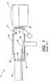
- FIG. 1is a somewhat schematic vertical cross-sectional view of a conventional processing tool 11 .
- the processing tool 11includes a centrally-positioned transfer chamber 13 .
- a load lock chamber 15 and a processing chamber 17are shown coupled to respective sides of the transfer chamber 13 .
- One or more additional process chambers and/or load lock chambers, which are not shown,may also be coupled to respective sides of the transfer chamber 13 .
- the load lock chamber 15is provided to accommodate introduction of substrates into the processing tool 11 from outside of the processing tool 11 .
- the transfer chamber 13includes a main body 19 having side walls 21 (of which only two are visible in FIG. 1 ). Each side wall 21 may be adapted to have a load lock or processing chamber coupled thereto.
- the transfer chamber 13also includes a top 23 supported on the main body 19 .
- a lid 25is provided to sealingly close the top 23 of the transfer chamber 13 .
- a lower end of the transfer chamber 13is closed by a substantially annular bottom 27 .
- the bottom 27 of the transfer chamber 13has a central aperture 29 which accommodates installation of a substrate handling robot 31 in the transfer chamber 13 .
- the substrate handling robot 31is adapted to transfer substrates among the processing chambers 17 and the load lock chamber or chambers 15 coupled to transfer chamber 13 .
- the processing tool 11may be referred to as a vacuum processing system.
- a pumping systemwhich is not shown, may be coupled to the transfer chamber 13 to pump the transfer chamber 13 down to a suitable degree of vacuum.
- FIG. 1Also illustrated in FIG. 1 is an actuator 33 which selectively opens and closes a slit valve 35 associated with the processing chamber 17 .
- a slit valve 35When the slit valve 35 is in an open position (not shown), a substrate may be introduced into or removed from the processing chamber 17 .
- the slit valve 35When the slit valve 35 is in the closed position illustrated in FIG. 1 , the processing chamber 17 is isolated from the transfer chamber 13 so that a fabrication process may be performed on a substrate within the processing chamber 17 .
- Processing toolsand in particular the transfer chamber portions thereof, are manufactured in a variety of sizes. In some cases it is necessary or desirable that the transfer chamber 13 be quite large. For example, in a processing tool used for fabricating flat panel displays, the glass plate substrates that are processed currently range from about 0.5 to 1.5 meters per side, and may reach 2-3 meters per side in the near future. Accordingly, a very large transfer chamber is required for such applications. In addition, it may be desirable to increase the number of processing chambers and/or load locks included in the processing tool, which also may require that the transfer chamber be made large. However, increasing the size of a transfer chamber increases vacuum induced stresses in components thereof such as the bottom of the transfer chamber. To accommodate such stresses, the thickness of the bottom of a transfer chamber may be increased to provide increased strength. However, increased thickness of the transfer chamber bottom results in greater weight, increased difficulty in manufacture, and higher cost.
- a transfer chamberincluding a main body having side walls adapted to couple to at least one processing chamber and at least one load lock chamber.
- the main bodyis also adapted to house at least a portion of a robot adapted to transport a substrate between the at least one processing chamber and the at least one load lock chamber.
- the inventive transfer chamberalso includes a lid adapted to couple to and to seal a top portion of the main body of the transfer chamber.
- the inventive transfer chamberfurther includes a domed bottom adapted to couple to and to seal a bottom portion of the main body of the transfer chamber.
- a vacuum processing systemincludes a transfer chamber as described above in connection with the first aspect of the invention.
- the inventive vacuum processing systemalso includes at least one processing chamber coupled to the main body of the transfer chamber and at least one load lock chamber coupled to the main body of the transfer chamber.
- the inventive vacuum processing systemfurther includes a robot that at least partially extends through the domed bottom into the transfer chamber. The robot is adapted to transport a substrate between the at least one processing chamber and the at least one load lock chamber via the transfer chamber.
- a method of forming a domed bottom for a transfer chamberis provided.
- the transfer chamberis adapted to couple at least one load lock chamber to at least one processing chamber.
- the methodincludes selecting a material and forming a domed bottom from the material.
- the domed bottomhas an outer diameter sized to fit against and configured to form a seal with a bottom portion of a main body of a transfer chamber.
- the domed bottomalso has an aperture having a diameter sized to accommodate at least a portion of a robot.
- the robotis adapted to transfer substrates between at least one load lock chamber and at least one processing chamber coupled to the transfer chamber.
- the inventive transfer chamber bottomexhibits greater strength than would a transfer chamber bottom of equal thickness having a flat configuration. Accordingly, the inventive transfer chamber bottom may be made thinner than conventional flat bottoms of transfer chambers of comparable size, thereby providing savings in cost and weight.
- FIG. 1is a vertical cross-sectional view of a conventional vacuum processing system
- FIG. 2is a vertical cross-sectional view of a vacuum processing system provided in accordance with a first embodiment of the invention
- FIG. 3is an exploded view of a transfer chamber that is part of the inventive vacuum processing system of FIG. 2 ;
- FIG. 4is a simplified schematic side view of an exemplary embodiment of the transfer chamber of FIGS. 2 and 3 ;
- FIG. 5is a schematic vertical cross-sectional view of a vacuum processing system provided in accordance with another embodiment of the invention.
- the bottom of a transfer chamberis provided in a domed configuration, thereby achieving greater strength for a given thickness of the bottom and reducing the interior volume of the transfer chamber.
- the bottom of the transfer chambermay be made thinner than conventional transfer chamber bottoms, so that a savings in cost and weight is realized.
- the reduced interior volume of the transfer chamberalso may decrease pump down times, thereby increasing throughput.
- FIGS. 2 and 3An embodiment of the invention will now be described with reference to FIGS. 2 and 3 .
- FIG. 2is a view similar to FIG. 1 of a processing tool (vacuum processing system) 201 provided in accordance with an embodiment of the present invention.
- the inventive processing tool 201includes a novel transfer chamber 203 .
- a conventional load lock chamber 15(which may be, for example, a double dual slot load lock (DDSL) or other conventional load lock) and a conventional processing chamber 17 are shown coupled to the inventive transfer chamber 203 . It will be understood that one or more additional process chambers and/or load lock chambers may also be coupled to the transfer chamber 203 , although not shown in the drawings.
- a substrate handling robot 205is disposed within the transfer chamber 203 . As with the conventional system of FIG.
- a pumping system(not shown) may be coupled to the inventive transfer chamber 203 to pump down the transfer chamber 203 to a suitable degree of vacuum.
- a pumping system(not shown) may be coupled to the inventive transfer chamber 203 to pump down the transfer chamber 203 to a suitable degree of vacuum.
- the inventive transfer chamber 203will be described with reference to both FIG. 2 and FIG. 3 (which is an exploded view of the inventive transfer chamber 203 ).
- the transfer chamber 203includes a main body 207 , which may be, for example, machined from a single piece of material such as aluminum. Other materials may be employed. As described further below, in at least one embodiment of the invention the height of the main body 207 (H mB ) is minimized so as to reduce the overall volume and weight of the transfer chamber 207 .
- the main body 207may have a cylindrical interior wall 209 and an exterior wall 211 having flat regions 213 which form side walls 215 ( FIG. 2 ) that are adapted to couple to processing chambers or load lock chambers. In at least one embodiment, each side wall 215 ( FIG.
- Each side wall 215may include one or more respective slits 217 ( FIG. 3 ) through which a substrate (not shown) may be transferred from the transfer chamber 203 to a processing chamber 17 , or vice versa, by the substrate handling robot 205 .
- a slit valve(not shown in FIGS. 2 and 3 ) may be associated with each slit 217 to selectively open and close each slit 217 . In the embodiment of FIGS.
- the transfer chamber 203includes two slits 217 a , 217 b for allowing substrates to be loaded into and out of the load lock chamber 15 at two different heights.
- the slits 217 a , 217 bmay be sealed, for example, via conventional gate valves 219 a , 219 b ( FIG. 2 ).
- the transfer chamber 203may employ slit valve actuators internal to the transfer chamber 203 , such as the slit valve actuator 33 of FIG. 1 , to seal or open the slits 217 (e.g., a conventional 45 degree-type slit valve).
- conventional gate valvese.g., external gate valve 221 ( FIG. 2 ) that moves vertically
- Such a configurationmay simplify the design of the domed bottom (described below) of the transfer chamber 203 .
- the inventive transfer chamber 203may also include a top member 223 which is annularly shaped, and is adapted to be sealingly joined to an upper portion of the main body 207 via a first O-ring 225 .
- the inventive transfer chamber 203may also include a lid 227 which is provided to sealingly close an aperture 229 of the top member 223 via a second O-ring 231 .
- Other sealing mechanismsmay be employed as may other configurations for sealing the top of the transfer chamber 203 .
- the transfer chamber 203also includes a bottom member 233 which has a domed configuration, as best seen in FIG. 2 .
- the bottom member 233has a concave configuration such that a vertical distance between the lid 227 of the transfer chamber 203 and a central portion of the bottom member 233 is greater than a vertical distance between the lid 227 and an outer edge of the bottom member 233 .
- the bottom member 233may be machined from a single piece of material such as stainless steel. Other materials and/or configurations may be used. Techniques that may be employed to manufacture the bottom member 233 are disclosed, for example, in co-pending U.S. patent application Ser. No. 09/523,366, filed Mar. 10, 2000 and entitled “Vacuum Processing System for Producing Components” (Attorney Docket No. 2801), which is incorporated herein by reference in its entirety. Such techniques may include, for example, spinning, rolling and/or the like.
- the bottom member 233may have a thickness of about 0.5 to 0.625 inches (e.g., in the domed region), as compared to a thickness of three inches for conventional bottom members having a flat configuration and of comparable size (e.g., with an outer diameter of about 2.6 meters). Other thicknesses may be employed.
- the bottom member 233is adapted to couple to and seal a bottom portion of the main body 207 via an outer edge 235 of the bottom member 233 and a third O-ring 237 .
- the bottom member 233has a generally circular central aperture 239 .
- the outer edge 235 and central aperture 239may be thicker than the remainder of the bottom member 233 (e.g., about two inches square in the above described embodiment) and may be separately formed and attached to the domed region (e.g., via welding).
- Various openings and/or surface features 241may be provided to accommodate sensors, vacuum ports, gas ports, etc.
- An annular plug member 243is provided to seal the central aperture 239 of the bottom member 233 via a fourth O-ring 245 .
- the plug member 243has a central aperture 247 sized to sealingly accommodate a portion of the substrate handling robot 205 ( FIG. 2 ) which extends through the central aperture 247 of the plug member 243 and through the central aperture 239 of the bottom member 233 .
- a fifth O-ring 249( FIG. 3 ) seals the central aperture 247 of the plug member 243 around the robot 205 .
- Other sealing mechanismsmay be employed in place of or in addition to the O-rings 237 , 245 and 249 .
- the present inventionprovides for a transfer chamber in which the bottom has a domed configuration. Consequently, for a given size of transfer chamber, the domed bottom can be formed of thinner material than a conventional flat bottom. As a result, the cost and weight of the transfer chamber bottom can be reduced. This may be particularly significant in the case of very large transfer chambers of the type employed with processing tools which process glass plates for fabrication of flat panel displays. Such a design may consume unused space underneath a transfer chamber and does not interfere with overhead height limitations (e.g., due to overhead factory transport systems, ceiling heights, etc.).
- the size of the glass plates transferred within a transfer chambercontinues to grow.
- Current glass plate sizesare in the range of about 0.5 to 1.5 meters per side.
- larger glass substratesare being developed (e.g., about 2-3 meters per side).
- Increasing glass plate sizerequires transfer chambers of increasing diameter (and larger load lock and process chambers for processing such larger substrates).
- the flat regions of a transfer chambere.g., flat regions 213 in FIG. 3
- transfer, load lock and process chamber sizesincrease, numerous factors should be considered during transfer chamber design, such as robot size, volume of the transfer chamber, space available underneath the transfer chamber, vacuum forces generated within the transfer chamber, weight of the transfer chamber, cost of the transfer chamber and the like.
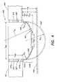
- FIG. 4is a simplified schematic side view of an exemplary embodiment of the transfer chamber 203 of FIGS. 2 and 3 .
- the transfer chamber 203is coupled to at least one load lock chamber 401 and at least one process chamber 403 , and includes the main body 207 as previously described.
- support structure for the transfer chamber 203 , and load lock and process chambers 401 , 403is not shown in FIG. 4 .
- the transfer chamber 203has a minimum transfer height H TR which represents the minimum height at which a substrate may be transferred within the transfer chamber 203 .
- the minimum transfer height H TRmay be an industry standard, a requirement of the fabrication facility employing the transfer chamber 203 , or the like.
- the minimum transfer height H TRis defined relative to a floor 405 of a facility (not shown) in which the transfer chamber 203 is located.
- the floor 405may be, for example, a floor of a clean room, a raised floor or any other lower limit on the space/area/height located below the transfer chamber 203 .
- the minimum transfer height H TRsets the height (H F ) that the transfer chamber 203 is positioned above the floor 405 .
- the volume below the transfer chamber 203 that may be employed to accommodate the domed bottom 233is approximately the volume of a cylinder having a diameter equal to the inner diameter of the main body 207 of the transfer chamber 203 (D MB ) and a height equal to the height of the transfer chamber 203 above the floor 405 (H F ).
- the domed bottom 233 of the transfer chamber 203includes a cylindrical region 233 a having a height H D1 and a domed region 233 b having a height H D2 . Accordingly, the volume of the domed bottom 233 is approximately equal to the volume of the cylindrical region 233 a plus the volume of the domed region 233 b.
- the transfer chamber 203have as small a volume as possible (e.g., to reduce pump down times thereby increasing throughput). Because a domed configuration defines a smaller volume than a cylindrical configuration (within the same predefined spatial region), from a volume consideration, it may be desirable to maximize the portion of the transfer chamber 203 that is domed (e.g., making the domed region 233 b of the domed bottom 233 larger while reducing both the height H D1 of the cylindrical region 233 a of the domed bottom 233 and the height H MB of the main body 207 ). However, other factors influence the selection of the height H MB of the main body 207 and the height H D1 of the cylindrical region 233 a of the domed bottom 233 .
- the height H MB of the main body 207 of the transfer chamber 203should be sufficient to accommodate any load lock chamber and/or process chamber coupled to the main body 207 .
- the height H MB of the main body 207may be set, for example, based on the minimum height required to accommodate the slit openings 217 a , 217 b that interface with the load lock chamber 401 .
- the height H D1 of the cylindrical region 233 a of the domed bottom 233should be sufficient to accommodate the height of the substrate transfer robot 205 ( FIG. 2 ).
- the substrate transfer robot 205includes a first arm 205 a and a second arm 205 b .
- the height H D1 of the cylindrical region 233 a of the domed bottom 233should be large enough to prevent the second arm 205 b of the robot 205 from extending into the domed region 233 b of the domed bottom 233 (whether the robot 205 is in a retracted position as shown in FIG. 2 or in an extended position such as is shown by the robot 31 of FIG. 1 ).
- the domed region 233 bmay contact and interfere with operation of the second arm 205 b .
- stiffness (and thus thickness) of each robot arm 205 a , 205 btypically increases.
- a corresponding increase in the height H D1 of the cylindrical region 233 b of the domed bottom 233may be employed to compensate for increased robot arm size.
- Another factor that may affect the design of the transfer chamber 203is the strength required for the domed bottom 233 . As transfer chamber size increases, so does the force exerted on the domed bottom 233 when the transfer chamber 203 is evacuated. Vacuum forces are most pronounced at the outer edge 235 of the domed bottom 233 ; and the domed bottom 233 should be sufficiently strong to resist vacuum induced deflections that may affect the ability of the domed bottom 233 to seal relative to the main body 207 of the transfer chamber 203 and/or the robot 205 ( FIG. 2 ).
- a spherical configuration for the domed bottom 233is preferred (as illustrated by domed bottom 233 ′ in FIG. 4 ). Such a configuration may be achieved by employing a radius of curvature (R D1′ ) of one half of the main body 207 's diameter (D MB ).
- R D1′radius of curvature
- D MBdiameter
- a spherical configuration for the domed bottom 233requires more space underneath the transfer chamber 203 (e.g., and may interfere with the floor 405 or another space limitation) and results in a transfer chamber having a large volume.
- a larger radius of curvaturemay be employed for a first portion 407 of the domed region 233 a of the domed bottom 233 .
- the radius of curvature R D1 of the first portion 407 of the domed bottom 233is greater than one half of the diameter D MB of the main body 207 of the transfer chamber 203 .
- the radius of curvature R D1is about 1.5 times the diameter D MB of the main body 207 of the transfer chamber 203 .
- Other valuesmay be employed. Selection of the radius of curvature R D1 may depend on many factors such as the space available under the transfer chamber 203 , the strength of the material employed for the domed bottom 233 , etc.
- the domed bottom 233may be provided with a second radiused portion 409 having a radius of curvature R D2 .
- This additional radius of curvaturecompensates for the mismatch between the radius of curvature R D1 of the first portion 407 of the domed bottom 233 and the radius of the main body 207 (one half of D MB ).
- the radius of curvature R D2 of the second portion 409is approximately 5-20 times the thickness of the domed bottom 233 (at its thinnest point).
- the transfer chamber 203 and/or the domed bottom 233may be designed as follows:
- the height H D1 of the cylindrical region 233 a of the domed bottom 233(e.g., based on the size of the robot 205 such as the thickness of the second arm 205 b , the minimum transfer height H TR of the transfer chamber 203 , the distance between the second arm 205 b and an end effector 205 c of the robot 205 ( FIG. 2 ), etc.); and/or
- the transfer chamber 203is configured as follows:
- radius of curvature R D1 of the radiused portion 407 of the domed bottom 233equals about 1.5 times the diameter of the main body 207 ;
- radius of curvature R D2 of the radiused portion 409 of the domed bottom 233equals about 5-20 times the thickness of the domed region 233 b ;
- thickness of the main body 207equals about 2 inches (at its thinnest point).
- exemplary support structure 241 for the transfer chamber 203 and/or the robot 205is illustrated.
- Such support structuremay include, for example, one or more suitably sized pedestal legs 243 , cross members 245 and/or braces 247 .
- any mechanism for supporting the transfer chamber 203 or the robot 205may be employed.
- the load lock chamber 15may be supported, for example, via a clean room wall 249 and/or the transfer chamber 205 ; and the processing chamber 17 may be supported, for example, by one or more pedestals 251 and/or cross members 253 .
- Other supporting configurationsmay be employed.
- the support structure 241is adapted to support the main body 207 of the transfer chamber 203 and the robot 205 without directly supporting the domed bottom 233 .
- pedestals 243may interface with flat regions 213 ( FIG. 3 ) of the main body 207 without contacting the domed bottom 233 ; and cross members 245 and braces 247 may support a main trunk 255 of the robot 205 without contacting the domed bottom 233 (as shown).
- the domed bottom 233may be supported by the main body 207 (e.g., by hanging therefrom, such as via bolts or other fastening mechanisms not shown).
- the domed bottom 233is isolated from the support structure 241 of the main body 207 and the robot 205 (and is “floating” relative to the main body 207 and the robot 205 ). Further in accordance with the above embodiment of the invention, a conventional bellows seal (not shown) may be employed between the domed bottom 233 and the robot 205 to allow the domed bottom 233 to move vertically relative the robot 205 without breaking a vacuum seal formed therebetween (e.g., via the o-rings 245 , 249 in FIG. 3 ).
- the domed bottom 233is free to deflect during evacuation and venting of the transfer chamber 203 , and fewer design constraints (e.g., in terms of material thickness, strength, etc.) are placed on the design of the domed bottom 233 . Further, deflections of the domed bottom 233 will not affect the position and/or calibration of the robot 205 .
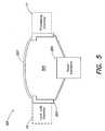
- FIG. 5is a schematic vertical cross-sectional view of a processing tool 501 provided in accordance with an alternative embodiment of the invention.
- the alternative inventive processing tool 501may be the same in all respects as the inventive processing tool 201 shown in FIG. 2 except that the processing tool 501 of FIG. 4 may have a transfer chamber 503 which has a lid 527 provided in a domed configuration (instead of employing the flat transfer chamber lid 227 shown in FIGS. 2 and 3 ).
- a transfer chamber lid having a domed configurationis disclosed in the above-referenced patent application Ser. No. 09/523,366 (Attorney Docket No. 2801).
- the domed transfer chamber bottomhas been illustrated above as having a concave configuration, the domed transfer chamber bottom may alternatively have a convex configuration (i.e., such that a vertical distance between a central portion of the domed bottom and the lid of the transfer chamber is less than a vertical distance between an outer edge of the domed bottom and the lid of the transfer chamber).
- a “domed” bottom or lidneed only have a portion thereof, such as an outer portion, domed or curved. The remainder of the bottom or lid may assume other shapes and/or may be flat.
- Such a domed bottom (or lid) designmay be based on one or more of transfer chamber height or width, the height or width available underneath a transfer chamber, or the like.
- the configuration of the lidmay be convex (as also disclosed in the above-referenced U.S. patent application Ser. No. 09/523,366) rather than the concave lid configuration shown in FIG. 5 .
- the present inventionis particularly advantageous when applied to a large transfer chamber of the type used in processing glass plates, the invention is also applicable to other types of processing tools, including those used to process silicon wafers.
- the inventionis applicable to transfer chambers adapted to couple to any number of processing chambers and to any number of load lock chambers.
- the transfer chamber components illustrated in FIG. 3can be combined with other components.
- the lid 227 and the top member 223can be combined to form a single piece that sealingly closes the top of the main body 207 of the transfer chamber 203 .
- the term “lid”should be understood to include one, two or more pieces which seal the top of a transfer chamber. It is also contemplated that components of the inventive transfer chamber shown as a single piece in FIG. 3 may be constituted by two or more pieces.
- bottom member 233 and the plug member 243could be combined to form a single integral piece that seals around a substrate handling robot.
- the inventive transfer chambermay be arranged to accommodate any type of substrate handling robot, including a “frog leg” style robot.
- the design of the domed bottommay be affected (e.g., the height of the non-domed portion of the bottom, the radii of the domed portion of the bottom, material thickness, etc.).
Landscapes
- Engineering & Computer Science (AREA)
- Chemical & Material Sciences (AREA)
- Computer Hardware Design (AREA)
- Condensed Matter Physics & Semiconductors (AREA)
- Power Engineering (AREA)
- Microelectronics & Electronic Packaging (AREA)
- Manufacturing & Machinery (AREA)
- General Physics & Mathematics (AREA)
- Physics & Mathematics (AREA)
- Metallurgy (AREA)
- Organic Chemistry (AREA)
- Chemical Kinetics & Catalysis (AREA)
- Mechanical Engineering (AREA)
- Materials Engineering (AREA)
- General Chemical & Material Sciences (AREA)
- Container, Conveyance, Adherence, Positioning, Of Wafer (AREA)
- Chemical Vapour Deposition (AREA)
- Drying Of Semiconductors (AREA)
Abstract
Description
- This application is a continuation of and claims priority from U.S. patent application Ser. No. 10/601,185, filed Jun. 20, 2003, which claims priority from U.S. Provisional Patent Application Ser. No. 60/390,629, filed Jun. 21, 2002 and from U.S. Provisional Patent Application Ser. No. 60/392,578, filed Jun. 28, 2002. All of the above applications are hereby incorporated by reference herein in their entirety.
- This invention is generally concerned with processing systems used for processing substrates, and is more particularly concerned with a transfer chamber for use in such a system.
- Conventional techniques for manufacturing flat panel displays or semiconductor devices entail applying a sequence of processes to a substrate such as a glass plate or a silicon wafer. The processes to be applied may include thermal processing, physical vapor deposition (PVD), chemical vapor deposition (CVD), etching, etc. Typically, each process in the sequence of processes is performed in a respective processing chamber. Accordingly, the substrates upon which the processes are performed must be transferred from one processing chamber to another.
- It is also conventional to incorporate a number of different processing chambers in a single processing tool, wherein the processing chambers are coupled around the periphery of a central transfer chamber.
FIG. 1 is a somewhat schematic vertical cross-sectional view of aconventional processing tool 11. Theprocessing tool 11 includes a centrally-positionedtransfer chamber 13. Aload lock chamber 15 and aprocessing chamber 17 are shown coupled to respective sides of thetransfer chamber 13. One or more additional process chambers and/or load lock chambers, which are not shown, may also be coupled to respective sides of thetransfer chamber 13. Theload lock chamber 15 is provided to accommodate introduction of substrates into theprocessing tool 11 from outside of theprocessing tool 11. - The
transfer chamber 13 includes amain body 19 having side walls21 (of which only two are visible inFIG. 1 ). Eachside wall 21 may be adapted to have a load lock or processing chamber coupled thereto. Thetransfer chamber 13 also includes a top23 supported on themain body 19. Alid 25 is provided to sealingly close thetop 23 of thetransfer chamber 13. - A lower end of the
transfer chamber 13 is closed by a substantiallyannular bottom 27. Thebottom 27 of thetransfer chamber 13 has acentral aperture 29 which accommodates installation of asubstrate handling robot 31 in thetransfer chamber 13. Thesubstrate handling robot 31 is adapted to transfer substrates among theprocessing chambers 17 and the load lock chamber orchambers 15 coupled totransfer chamber 13. - To minimize the possibility of contamination of substrates processed in the
processing tool 11, it is customary to maintain a vacuum in the interior of thetransfer chamber 13. Hence, theprocessing tool 11 may be referred to as a vacuum processing system. A pumping system, which is not shown, may be coupled to thetransfer chamber 13 to pump thetransfer chamber 13 down to a suitable degree of vacuum. - Also illustrated in
FIG. 1 is anactuator 33 which selectively opens and closes aslit valve 35 associated with theprocessing chamber 17. When theslit valve 35 is in an open position (not shown), a substrate may be introduced into or removed from theprocessing chamber 17. When theslit valve 35 is in the closed position illustrated inFIG. 1 , theprocessing chamber 17 is isolated from thetransfer chamber 13 so that a fabrication process may be performed on a substrate within theprocessing chamber 17. - Processing tools, and in particular the transfer chamber portions thereof, are manufactured in a variety of sizes. In some cases it is necessary or desirable that the
transfer chamber 13 be quite large. For example, in a processing tool used for fabricating flat panel displays, the glass plate substrates that are processed currently range from about 0.5 to 1.5 meters per side, and may reach 2-3 meters per side in the near future. Accordingly, a very large transfer chamber is required for such applications. In addition, it may be desirable to increase the number of processing chambers and/or load locks included in the processing tool, which also may require that the transfer chamber be made large. However, increasing the size of a transfer chamber increases vacuum induced stresses in components thereof such as the bottom of the transfer chamber. To accommodate such stresses, the thickness of the bottom of a transfer chamber may be increased to provide increased strength. However, increased thickness of the transfer chamber bottom results in greater weight, increased difficulty in manufacture, and higher cost. - According to a first aspect of the invention, a transfer chamber is provided, including a main body having side walls adapted to couple to at least one processing chamber and at least one load lock chamber. The main body is also adapted to house at least a portion of a robot adapted to transport a substrate between the at least one processing chamber and the at least one load lock chamber. The inventive transfer chamber also includes a lid adapted to couple to and to seal a top portion of the main body of the transfer chamber. The inventive transfer chamber further includes a domed bottom adapted to couple to and to seal a bottom portion of the main body of the transfer chamber.
- According to a second aspect of the invention, a vacuum processing system includes a transfer chamber as described above in connection with the first aspect of the invention. The inventive vacuum processing system also includes at least one processing chamber coupled to the main body of the transfer chamber and at least one load lock chamber coupled to the main body of the transfer chamber. The inventive vacuum processing system further includes a robot that at least partially extends through the domed bottom into the transfer chamber. The robot is adapted to transport a substrate between the at least one processing chamber and the at least one load lock chamber via the transfer chamber.
- According to a third aspect of the invention, a method of forming a domed bottom for a transfer chamber is provided. The transfer chamber is adapted to couple at least one load lock chamber to at least one processing chamber. The method includes selecting a material and forming a domed bottom from the material. The domed bottom has an outer diameter sized to fit against and configured to form a seal with a bottom portion of a main body of a transfer chamber. The domed bottom also has an aperture having a diameter sized to accommodate at least a portion of a robot. The robot is adapted to transfer substrates between at least one load lock chamber and at least one processing chamber coupled to the transfer chamber.
- Because the transfer chamber bottom provided in accordance with the invention has a domed configuration, the inventive transfer chamber bottom exhibits greater strength than would a transfer chamber bottom of equal thickness having a flat configuration. Accordingly, the inventive transfer chamber bottom may be made thinner than conventional flat bottoms of transfer chambers of comparable size, thereby providing savings in cost and weight.
- Further features and advantages of the present invention will become more fully apparent from the following detailed description of exemplary embodiments, the appended claims and the accompanying drawings.
FIG. 1 is a vertical cross-sectional view of a conventional vacuum processing system;FIG. 2 is a vertical cross-sectional view of a vacuum processing system provided in accordance with a first embodiment of the invention;FIG. 3 is an exploded view of a transfer chamber that is part of the inventive vacuum processing system ofFIG. 2 ;FIG. 4 is a simplified schematic side view of an exemplary embodiment of the transfer chamber ofFIGS. 2 and 3 ; andFIG. 5 is a schematic vertical cross-sectional view of a vacuum processing system provided in accordance with another embodiment of the invention.- In accordance with the invention, the bottom of a transfer chamber is provided in a domed configuration, thereby achieving greater strength for a given thickness of the bottom and reducing the interior volume of the transfer chamber. As a result, the bottom of the transfer chamber may be made thinner than conventional transfer chamber bottoms, so that a savings in cost and weight is realized. The reduced interior volume of the transfer chamber also may decrease pump down times, thereby increasing throughput.
- An embodiment of the invention will now be described with reference to
FIGS. 2 and 3 . FIG. 2 is a view similar toFIG. 1 of a processing tool (vacuum processing system)201 provided in accordance with an embodiment of the present invention. Theinventive processing tool 201 includes anovel transfer chamber 203. A conventional load lock chamber15 (which may be, for example, a double dual slot load lock (DDSL) or other conventional load lock) and aconventional processing chamber 17 are shown coupled to theinventive transfer chamber 203. It will be understood that one or more additional process chambers and/or load lock chambers may also be coupled to thetransfer chamber 203, although not shown in the drawings. Asubstrate handling robot 205 is disposed within thetransfer chamber 203. As with the conventional system ofFIG. 1 , a pumping system (not shown) may be coupled to theinventive transfer chamber 203 to pump down thetransfer chamber 203 to a suitable degree of vacuum. For convenience, theinventive transfer chamber 203 will be described with reference to bothFIG. 2 andFIG. 3 (which is an exploded view of the inventive transfer chamber203).- With reference to
FIGS. 2 and 3 , thetransfer chamber 203 includes amain body 207, which may be, for example, machined from a single piece of material such as aluminum. Other materials may be employed. As described further below, in at least one embodiment of the invention the height of the main body207 (HmB) is minimized so as to reduce the overall volume and weight of thetransfer chamber 207. Themain body 207 may have a cylindricalinterior wall 209 and anexterior wall 211 havingflat regions 213 which form side walls215 (FIG. 2 ) that are adapted to couple to processing chambers or load lock chambers. In at least one embodiment, each side wall215 (FIG. 2 ) may, for example, have a thickness of about two inches at its thinnest point (e.g., the center of each flat region213). Other side wall thicknesses may be employed. Eachside wall 215 may include one or more respective slits217 (FIG. 3 ) through which a substrate (not shown) may be transferred from thetransfer chamber 203 to aprocessing chamber 17, or vice versa, by thesubstrate handling robot 205. A slit valve (not shown inFIGS. 2 and 3 ) may be associated with eachslit 217 to selectively open and close eachslit 217. In the embodiment ofFIGS. 2 and 3 , thetransfer chamber 203 includes twoslits load lock chamber 15 at two different heights. Theslits conventional gate valves FIG. 2 ). - Although not shown in
FIG. 2 or3, thetransfer chamber 203 may employ slit valve actuators internal to thetransfer chamber 203, such as theslit valve actuator 33 ofFIG. 1 , to seal or open the slits217 (e.g., a conventional 45 degree-type slit valve). Alternatively, in at least one embodiment, conventional gate valves (e.g., external gate valve221 (FIG. 2 ) that moves vertically) may be positioned outside thetransfer chamber 203 to seal and open theslits 217. Such a configuration may simplify the design of the domed bottom (described below) of thetransfer chamber 203. - Referring again to
FIG. 3 , theinventive transfer chamber 203 may also include atop member 223 which is annularly shaped, and is adapted to be sealingly joined to an upper portion of themain body 207 via a first O-ring 225. Theinventive transfer chamber 203 may also include alid 227 which is provided to sealingly close anaperture 229 of thetop member 223 via a second O-ring 231. Other sealing mechanisms may be employed as may other configurations for sealing the top of thetransfer chamber 203. - In accordance with the invention, the
transfer chamber 203 also includes abottom member 233 which has a domed configuration, as best seen inFIG. 2 . As will be observed fromFIG. 2 , thebottom member 233 has a concave configuration such that a vertical distance between thelid 227 of thetransfer chamber 203 and a central portion of thebottom member 233 is greater than a vertical distance between thelid 227 and an outer edge of thebottom member 233. In one embodiment of the invention, thebottom member 233 may be machined from a single piece of material such as stainless steel. Other materials and/or configurations may be used. Techniques that may be employed to manufacture thebottom member 233 are disclosed, for example, in co-pending U.S. patent application Ser. No. 09/523,366, filed Mar. 10, 2000 and entitled “Vacuum Processing System for Producing Components” (Attorney Docket No. 2801), which is incorporated herein by reference in its entirety. Such techniques may include, for example, spinning, rolling and/or the like. - In one embodiment, the
bottom member 233 may have a thickness of about 0.5 to 0.625 inches (e.g., in the domed region), as compared to a thickness of three inches for conventional bottom members having a flat configuration and of comparable size (e.g., with an outer diameter of about 2.6 meters). Other thicknesses may be employed. - Referring again to
FIG. 3 , thebottom member 233 is adapted to couple to and seal a bottom portion of themain body 207 via anouter edge 235 of thebottom member 233 and a third O-ring 237. Thebottom member 233 has a generally circularcentral aperture 239. Theouter edge 235 andcentral aperture 239 may be thicker than the remainder of the bottom member233 (e.g., about two inches square in the above described embodiment) and may be separately formed and attached to the domed region (e.g., via welding). Various openings and/or surface features241 may be provided to accommodate sensors, vacuum ports, gas ports, etc. Anannular plug member 243 is provided to seal thecentral aperture 239 of thebottom member 233 via a fourth O-ring 245. Theplug member 243 has acentral aperture 247 sized to sealingly accommodate a portion of the substrate handling robot205 (FIG. 2 ) which extends through thecentral aperture 247 of theplug member 243 and through thecentral aperture 239 of thebottom member 233. A fifth O-ring249 (FIG. 3 ) seals thecentral aperture 247 of theplug member 243 around therobot 205. Other sealing mechanisms may be employed in place of or in addition to the O-rings - The present invention provides for a transfer chamber in which the bottom has a domed configuration. Consequently, for a given size of transfer chamber, the domed bottom can be formed of thinner material than a conventional flat bottom. As a result, the cost and weight of the transfer chamber bottom can be reduced. This may be particularly significant in the case of very large transfer chambers of the type employed with processing tools which process glass plates for fabrication of flat panel displays. Such a design may consume unused space underneath a transfer chamber and does not interfere with overhead height limitations (e.g., due to overhead factory transport systems, ceiling heights, etc.).
- As the flat panel industry continues to mature, the size of the glass plates transferred within a transfer chamber (such as the transfer chamber203) continues to grow. Current glass plate sizes are in the range of about 0.5 to 1.5 meters per side. However, larger glass substrates are being developed (e.g., about 2-3 meters per side). Increasing glass plate size requires transfer chambers of increasing diameter (and larger load lock and process chambers for processing such larger substrates). In the near future, the flat regions of a transfer chamber (e.g.,
flat regions 213 inFIG. 3 ) may reach dimensions of greater than about 2-4 meters to accommodate similarly sized glass substrates. As transfer, load lock and process chamber sizes increase, numerous factors should be considered during transfer chamber design, such as robot size, volume of the transfer chamber, space available underneath the transfer chamber, vacuum forces generated within the transfer chamber, weight of the transfer chamber, cost of the transfer chamber and the like. FIG. 4 is a simplified schematic side view of an exemplary embodiment of thetransfer chamber 203 ofFIGS. 2 and 3 . InFIG. 4 , thetransfer chamber 203 is coupled to at least oneload lock chamber 401 and at least oneprocess chamber 403, and includes themain body 207 as previously described. For clarity, support structure for thetransfer chamber 203, and load lock andprocess chambers FIG. 4 .- One parameter relevant to the design of the
transfer chamber 203 is the space available underneath thetransfer chamber 203 to accommodate thedomed bottom 233. With reference toFIG. 4 , thetransfer chamber 203 has a minimum transfer height HTRwhich represents the minimum height at which a substrate may be transferred within thetransfer chamber 203. The minimum transfer height HTRmay be an industry standard, a requirement of the fabrication facility employing thetransfer chamber 203, or the like. In the example ofFIG. 4 , the minimum transfer height HTRis defined relative to afloor 405 of a facility (not shown) in which thetransfer chamber 203 is located. Thefloor 405 may be, for example, a floor of a clean room, a raised floor or any other lower limit on the space/area/height located below thetransfer chamber 203. - The minimum transfer height HTRsets the height (HF) that the
transfer chamber 203 is positioned above thefloor 405. The volume below thetransfer chamber 203 that may be employed to accommodate thedomed bottom 233 is approximately the volume of a cylinder having a diameter equal to the inner diameter of themain body 207 of the transfer chamber203 (DMB) and a height equal to the height of thetransfer chamber 203 above the floor405 (HF). - As shown in
FIG. 4 , thedomed bottom 233 of thetransfer chamber 203 includes acylindrical region 233ahaving a height HD1and adomed region 233bhaving a height HD2. Accordingly, the volume of thedomed bottom 233 is approximately equal to the volume of thecylindrical region 233aplus the volume of thedomed region 233b. - It is often preferable that the
transfer chamber 203 have as small a volume as possible (e.g., to reduce pump down times thereby increasing throughput). Because a domed configuration defines a smaller volume than a cylindrical configuration (within the same predefined spatial region), from a volume consideration, it may be desirable to maximize the portion of thetransfer chamber 203 that is domed (e.g., making thedomed region 233bof thedomed bottom 233 larger while reducing both the height HD1of thecylindrical region 233aof thedomed bottom 233 and the height HMBof the main body207). However, other factors influence the selection of the height HMBof themain body 207 and the height HD1of thecylindrical region 233aof thedomed bottom 233. For example, the height HMBof themain body 207 of thetransfer chamber 203 should be sufficient to accommodate any load lock chamber and/or process chamber coupled to themain body 207. In at least one embodiment of the invention, the height HMBof themain body 207 may be set, for example, based on the minimum height required to accommodate theslit openings load lock chamber 401. - With regard to the height HD1of the
cylindrical region 233aof thedomed bottom 233, the height HD1should be sufficient to accommodate the height of the substrate transfer robot205 (FIG. 2 ). As shown inFIG. 2 , thesubstrate transfer robot 205 includes afirst arm 205aand asecond arm 205b. When thesubstrate transfer robot 205 is positioned to transfer a substrate at a height near the minimum transfer height HTR, such as through theopening 217bof themain body 207 of thetransfer chamber 203, the height HD1of thecylindrical region 233aof thedomed bottom 233 should be large enough to prevent thesecond arm 205bof therobot 205 from extending into thedomed region 233bof the domed bottom233 (whether therobot 205 is in a retracted position as shown inFIG. 2 or in an extended position such as is shown by therobot 31 ofFIG. 1 ). If the height HD1of thecylindrical region 233aof thedomed bottom 233 is not large enough to prevent thesecond arm 205bfrom extending into thedomed region 233bof thedomed bottom 233, thedomed region 233bmay contact and interfere with operation of thesecond arm 205b. As glass substrate size and transfer chamber size increase, stiffness (and thus thickness) of eachrobot arm cylindrical region 233bof thedomed bottom 233 may be employed to compensate for increased robot arm size. - Another factor that may affect the design of the
transfer chamber 203 is the strength required for thedomed bottom 233. As transfer chamber size increases, so does the force exerted on thedomed bottom 233 when thetransfer chamber 203 is evacuated. Vacuum forces are most pronounced at theouter edge 235 of thedomed bottom 233; and thedomed bottom 233 should be sufficiently strong to resist vacuum induced deflections that may affect the ability of thedomed bottom 233 to seal relative to themain body 207 of thetransfer chamber 203 and/or the robot205 (FIG. 2 ). - From a strength standpoint, a spherical configuration for the
domed bottom 233 is preferred (as illustrated bydomed bottom 233′ inFIG. 4 ). Such a configuration may be achieved by employing a radius of curvature (RD1′) of one half of themain body 207's diameter (DMB). However, as shown inFIG. 4 , a spherical configuration for thedomed bottom 233 requires more space underneath the transfer chamber203 (e.g., and may interfere with thefloor 405 or another space limitation) and results in a transfer chamber having a large volume. To reduce the space/volume requirements of thedomed bottom 233, a larger radius of curvature (RD1) may be employed for afirst portion 407 of thedomed region 233aof thedomed bottom 233. In at least one embodiment, the radius of curvature RD1of thefirst portion 407 of thedomed bottom 233 is greater than one half of the diameter DMBof themain body 207 of thetransfer chamber 203. In one particular embodiment, the radius of curvature RD1is about 1.5 times the diameter DMBof themain body 207 of thetransfer chamber 203. Other values may be employed. Selection of the radius of curvature RD1may depend on many factors such as the space available under thetransfer chamber 203, the strength of the material employed for thedomed bottom 233, etc. - When the radius of curvature RD1of the
first portion 407 of thedomed bottom 233 is greater than one half of the diameter DMBof themain body 207 of thetransfer chamber 203, thedomed bottom 233 may be provided with a secondradiused portion 409 having a radius of curvature RD2. This additional radius of curvature compensates for the mismatch between the radius of curvature RD1of thefirst portion 407 of thedomed bottom 233 and the radius of the main body207 (one half of DMB). In at least one embodiment of the invention, the radius of curvature RD2of thesecond portion 409 is approximately 5-20 times the thickness of the domed bottom233 (at its thinnest point). - Based on the foregoing and in accordance with the present invention, the
transfer chamber 203 and/or thedomed bottom 233 may be designed as follows: - (1) determine the space underneath the
transfer chamber 203 available for the domed bottom233 (e.g., based on minimum transfer height HTRand/or the height HFOf thetransfer chamber 203 above any interfering structure such as the floor405); - (2) determine the radius of curvature RD1for the
first portion 407 of the domed bottom233 (e.g., based on the height HFof thetransfer chamber 203 above thefloor 405, minimum transfer height HTR, desired overall size of thetransfer chamber 203, dimensions of therobot 205 such as width and height, the amount of deflection of thedomed bottom 233 that is tolerable, the vacuum levels to be employed within thetransfer chamber 203, etc.); - (3) determine the thickness of the domed bottom233 (e.g., based on the radius of curvature RD1for the
first portion 407 of thedomed bottom 233, material strength, the amount of deflection of thedomed bottom 233 that is tolerable, the vacuum levels to be employed within thetransfer chamber 203, etc.); - (4) determine the height HMBof the
main body 207 of the transfer chamber203 (e.g., based on the size of the load lock and/or process chambers to be coupled to themain body 207, the height required to accommodate the slit openings used to interface the load lock and/or process chambers to be coupled to themain body 207, etc.);
- (1) determine the space underneath the
- (5) determine the height HD1of the
cylindrical region 233aof the domed bottom233 (e.g., based on the size of therobot 205 such as the thickness of thesecond arm 205b, the minimum transfer height HTRof thetransfer chamber 203, the distance between thesecond arm 205band anend effector 205cof the robot205 (FIG. 2 ), etc.); and/or - (6) determine the radius of curvature RD2for the
second portion 409 of the domed bottom233 (e.g., based on the radius of curvature RD1of thefirst portion 407 of thedomed bottom 233, the height HD1of thecylindrical region 233aof thedomed bottom 233, etc.)
Any of the above factors may be employed alone or in combination, and in any order for designing one or more of thetransfer chamber 203 and/or thedomed bottom 233. Other factors may be considered during design of thetransfer chamber 203 and/or thedomed bottom 233, such as the diameter (DDB) of the aperture required to accommodate therobot 205, the affect of such an aperture on domed bottom strength, or the like.
- (6) determine the radius of curvature RD2for the
- In one exemplary embodiment of the invention, the
transfer chamber 203 is configured as follows: - (1) diameter DMBof the
main body 207 equals about 2.6 meters; - (2) height HMBof the
main body 207 equals about 0.8 meters; - (3) height HD1of the
cylindrical region 233aof thedomed bottom 233 equals about 6 inches; - (4) height HD2of the
domed region 233bof thedomed bottom 233 equals about 12 inches; - (5) thickness of the cylindrical and
domed regions domed bottom 233 equals about 0.5-0.625 inches;
- (1) diameter DMBof the
- (6) radius of curvature RD1of the radiused
portion 407 of thedomed bottom 233 equals about 1.5 times the diameter of themain body 207; - (7) radius of curvature RD2of the radiused
portion 409 of thedomed bottom 233 equals about 5-20 times the thickness of thedomed region 233b; and - (8) thickness of the
main body 207 equals about 2 inches (at its thinnest point). - Other transfer chamber configurations may be employed.
- Referring again to
FIG. 2 ,exemplary support structure 241 for thetransfer chamber 203 and/or therobot 205 is illustrated. Such support structure may include, for example, one or more suitablysized pedestal legs 243,cross members 245 and/or braces247. In general, any mechanism for supporting thetransfer chamber 203 or therobot 205 may be employed. Theload lock chamber 15 may be supported, for example, via aclean room wall 249 and/or thetransfer chamber 205; and theprocessing chamber 17 may be supported, for example, by one ormore pedestals 251 and/orcross members 253. Other supporting configurations may be employed. - In at least one embodiment of the invention, the
support structure 241 is adapted to support themain body 207 of thetransfer chamber 203 and therobot 205 without directly supporting thedomed bottom 233. For example, pedestals243 may interface with flat regions213 (FIG. 3 ) of themain body 207 without contacting thedomed bottom 233; andcross members 245 and braces247 may support amain trunk 255 of therobot 205 without contacting the domed bottom233 (as shown). Thedomed bottom 233 may be supported by the main body207 (e.g., by hanging therefrom, such as via bolts or other fastening mechanisms not shown). - In the above described embodiment, the
domed bottom 233 is isolated from thesupport structure 241 of themain body 207 and the robot205 (and is “floating” relative to themain body 207 and the robot205). Further in accordance with the above embodiment of the invention, a conventional bellows seal (not shown) may be employed between thedomed bottom 233 and therobot 205 to allow thedomed bottom 233 to move vertically relative therobot 205 without breaking a vacuum seal formed therebetween (e.g., via the o-rings FIG. 3 ). In this manner, thedomed bottom 233 is free to deflect during evacuation and venting of thetransfer chamber 203, and fewer design constraints (e.g., in terms of material thickness, strength, etc.) are placed on the design of thedomed bottom 233. Further, deflections of thedomed bottom 233 will not affect the position and/or calibration of therobot 205. FIG. 5 is a schematic vertical cross-sectional view of aprocessing tool 501 provided in accordance with an alternative embodiment of the invention. The alternativeinventive processing tool 501 may be the same in all respects as theinventive processing tool 201 shown inFIG. 2 except that theprocessing tool 501 ofFIG. 4 may have atransfer chamber 503 which has alid 527 provided in a domed configuration (instead of employing the flattransfer chamber lid 227 shown inFIGS. 2 and 3 ). A transfer chamber lid having a domed configuration is disclosed in the above-referenced patent application Ser. No. 09/523,366 (Attorney Docket No. 2801).- The foregoing description discloses only exemplary embodiments of the invention; modifications of the above disclosed apparatus which fall within the scope of the invention will be readily apparent to those of ordinary skill in the art. For example, although the inventive domed transfer chamber bottom has been illustrated above as having a concave configuration, the domed transfer chamber bottom may alternatively have a convex configuration (i.e., such that a vertical distance between a central portion of the domed bottom and the lid of the transfer chamber is less than a vertical distance between an outer edge of the domed bottom and the lid of the transfer chamber). As used herein, a “domed” bottom or lid need only have a portion thereof, such as an outer portion, domed or curved. The remainder of the bottom or lid may assume other shapes and/or may be flat. Such a domed bottom (or lid) design may be based on one or more of transfer chamber height or width, the height or width available underneath a transfer chamber, or the like.
- It should further be recognized that if a domed lid is employed, as shown in the embodiment of
FIG. 5 , the configuration of the lid may be convex (as also disclosed in the above-referenced U.S. patent application Ser. No. 09/523,366) rather than the concave lid configuration shown inFIG. 5 . - Although the present invention is particularly advantageous when applied to a large transfer chamber of the type used in processing glass plates, the invention is also applicable to other types of processing tools, including those used to process silicon wafers. The invention is applicable to transfer chambers adapted to couple to any number of processing chambers and to any number of load lock chambers.
- It should be understood that at least some of the transfer chamber components illustrated in
FIG. 3 can be combined with other components. For example, thelid 227 and thetop member 223 can be combined to form a single piece that sealingly closes the top of themain body 207 of thetransfer chamber 203. Accordingly, as used in the appended claims, the term “lid” should be understood to include one, two or more pieces which seal the top of a transfer chamber. It is also contemplated that components of the inventive transfer chamber shown as a single piece inFIG. 3 may be constituted by two or more pieces. - As another alternative, the
bottom member 233 and theplug member 243 could be combined to form a single integral piece that seals around a substrate handling robot. - The inventive transfer chamber may be arranged to accommodate any type of substrate handling robot, including a “frog leg” style robot.
- If the bottom of the transfer chamber is employed to support the weight of the main body of the transfer chamber and/or a portion of the weight of each load lock and process chamber coupled to the transfer chamber (e.g., if the domed bottom is not floating relative to the main body), the design of the domed bottom may be affected (e.g., the height of the non-domed portion of the bottom, the radii of the domed portion of the bottom, material thickness, etc.).
- Accordingly, while the present invention has been disclosed in connection with exemplary embodiments thereof, it should be understood that other embodiments may fall within the spirit and scope of the invention, as defined by the following claims.
Claims (31)
Priority Applications (1)
| Application Number | Priority Date | Filing Date | Title |
|---|---|---|---|
| US11/386,257US8033772B2 (en) | 2002-06-21 | 2006-03-21 | Transfer chamber for vacuum processing system |
Applications Claiming Priority (4)
| Application Number | Priority Date | Filing Date | Title |
|---|---|---|---|
| US39062902P | 2002-06-21 | 2002-06-21 | |
| US39257802P | 2002-06-28 | 2002-06-28 | |
| US10/601,185US7018517B2 (en) | 2002-06-21 | 2003-06-20 | Transfer chamber for vacuum processing system |
| US11/386,257US8033772B2 (en) | 2002-06-21 | 2006-03-21 | Transfer chamber for vacuum processing system |
Related Parent Applications (1)
| Application Number | Title | Priority Date | Filing Date |
|---|---|---|---|
| US10/601,185ContinuationUS7018517B2 (en) | 2002-06-21 | 2003-06-20 | Transfer chamber for vacuum processing system |
Publications (2)
| Publication Number | Publication Date |
|---|---|
| US20060157340A1true US20060157340A1 (en) | 2006-07-20 |
| US8033772B2 US8033772B2 (en) | 2011-10-11 |
Family
ID=30003165
Family Applications (2)
| Application Number | Title | Priority Date | Filing Date |
|---|---|---|---|
| US10/601,185Expired - LifetimeUS7018517B2 (en) | 2002-06-21 | 2003-06-20 | Transfer chamber for vacuum processing system |
| US11/386,257Expired - Fee RelatedUS8033772B2 (en) | 2002-06-21 | 2006-03-21 | Transfer chamber for vacuum processing system |
Family Applications Before (1)
| Application Number | Title | Priority Date | Filing Date |
|---|---|---|---|
| US10/601,185Expired - LifetimeUS7018517B2 (en) | 2002-06-21 | 2003-06-20 | Transfer chamber for vacuum processing system |
Country Status (8)
| Country | Link |
|---|---|
| US (2) | US7018517B2 (en) |
| EP (1) | EP1523761A1 (en) |
| JP (2) | JP4619116B2 (en) |
| KR (1) | KR100682209B1 (en) |
| CN (1) | CN100423179C (en) |
| AU (1) | AU2003245592A1 (en) |
| TW (1) | TWI294155B (en) |
| WO (1) | WO2004001817A1 (en) |
Cited By (12)
| Publication number | Priority date | Publication date | Assignee | Title |
|---|---|---|---|---|
| US20060051507A1 (en)* | 2004-06-02 | 2006-03-09 | Applied Materials, Inc. | Electronic device manufacturing chamber and methods of forming the same |
| US20060101728A1 (en)* | 2004-06-02 | 2006-05-18 | White John M | Electronic device manufacturing chamber and methods of forming the same |
| US20060201074A1 (en)* | 2004-06-02 | 2006-09-14 | Shinichi Kurita | Electronic device manufacturing chamber and methods of forming the same |
| US10998209B2 (en) | 2019-05-31 | 2021-05-04 | Applied Materials, Inc. | Substrate processing platforms including multiple processing chambers |
| US11600507B2 (en) | 2020-09-09 | 2023-03-07 | Applied Materials, Inc. | Pedestal assembly for a substrate processing chamber |
| US11610799B2 (en) | 2020-09-18 | 2023-03-21 | Applied Materials, Inc. | Electrostatic chuck having a heating and chucking capabilities |
| US11674227B2 (en) | 2021-02-03 | 2023-06-13 | Applied Materials, Inc. | Symmetric pump down mini-volume with laminar flow cavity gas injection for high and low pressure |
| US11749542B2 (en) | 2020-07-27 | 2023-09-05 | Applied Materials, Inc. | Apparatus, system, and method for non-contact temperature monitoring of substrate supports |
| US11817331B2 (en) | 2020-07-27 | 2023-11-14 | Applied Materials, Inc. | Substrate holder replacement with protective disk during pasting process |
| US12002668B2 (en) | 2021-06-25 | 2024-06-04 | Applied Materials, Inc. | Thermal management hardware for uniform temperature control for enhanced bake-out for cluster tool |
| US12080571B2 (en) | 2020-07-08 | 2024-09-03 | Applied Materials, Inc. | Substrate processing module and method of moving a workpiece |
| US12195314B2 (en) | 2021-02-02 | 2025-01-14 | Applied Materials, Inc. | Cathode exchange mechanism to improve preventative maintenance time for cluster system |
Families Citing this family (39)
| Publication number | Priority date | Publication date | Assignee | Title |
|---|---|---|---|---|
| CN100423179C (en) | 2002-06-21 | 2008-10-01 | 应用材料股份有限公司 | Transfer chambers for vacuum processing systems |
| US7393439B2 (en)* | 2003-06-06 | 2008-07-01 | Semitool, Inc. | Integrated microfeature workpiece processing tools with registration systems for paddle reactors |
| US20050035046A1 (en)* | 2003-06-06 | 2005-02-17 | Hanson Kyle M. | Wet chemical processing chambers for processing microfeature workpieces |
| US20050063798A1 (en)* | 2003-06-06 | 2005-03-24 | Davis Jeffry Alan | Interchangeable workpiece handling apparatus and associated tool for processing microfeature workpieces |
| US20050050767A1 (en)* | 2003-06-06 | 2005-03-10 | Hanson Kyle M. | Wet chemical processing chambers for processing microfeature workpieces |
| US20070144912A1 (en)* | 2003-07-01 | 2007-06-28 | Woodruff Daniel J | Linearly translating agitators for processing microfeature workpieces, and associated methods |
| US20070269297A1 (en)* | 2003-11-10 | 2007-11-22 | Meulen Peter V D | Semiconductor wafer handling and transport |
| US7458763B2 (en) | 2003-11-10 | 2008-12-02 | Blueshift Technologies, Inc. | Mid-entry load lock for semiconductor handling system |
| US10086511B2 (en) | 2003-11-10 | 2018-10-02 | Brooks Automation, Inc. | Semiconductor manufacturing systems |
| US8083853B2 (en) | 2004-05-12 | 2011-12-27 | Applied Materials, Inc. | Plasma uniformity control by gas diffuser hole design |
| US7354845B2 (en)* | 2004-08-24 | 2008-04-08 | Otb Group B.V. | In-line process for making thin film electronic devices |
| US8328939B2 (en)* | 2004-05-12 | 2012-12-11 | Applied Materials, Inc. | Diffuser plate with slit valve compensation |
| KR100716041B1 (en)* | 2004-06-02 | 2007-05-09 | 어플라이드 머티어리얼스, 인코포레이티드 | Methods and apparatus for sealing a chamber |
| CN1767147B (en)* | 2004-06-02 | 2015-08-19 | 应用材料公司 | Electronic device manufacturing chamber and method for forming the same |
| US8648977B2 (en)* | 2004-06-02 | 2014-02-11 | Applied Materials, Inc. | Methods and apparatus for providing a floating seal having an isolated sealing surface for chamber doors |
| WO2006130811A2 (en)* | 2005-06-02 | 2006-12-07 | Applied Materials, Inc. | Electronic device manufacturing chamber and methods of forming the same |
| KR20070082056A (en)* | 2006-02-14 | 2007-08-20 | 브룩스오토메이션아시아(주) | Transfer chamber for substrate vacuum processing device |
| US20080178460A1 (en)* | 2007-01-29 | 2008-07-31 | Woodruff Daniel J | Protected magnets and magnet shielding for processing microfeature workpieces, and associated systems and methods |
| US20080276867A1 (en) | 2007-05-09 | 2008-11-13 | Jason Schaller | Transfer chamber with vacuum extension for shutter disks |
| US7871510B2 (en)* | 2007-08-28 | 2011-01-18 | Exxonmobil Research & Engineering Co. | Production of an enhanced resid coker feed using ultrafiltration |
| US7897828B2 (en)* | 2007-08-28 | 2011-03-01 | Exxonmobile Research And Engineering Company | Process for separating a heavy oil feedstream into improved products |
| US7867379B2 (en)* | 2007-08-28 | 2011-01-11 | Exxonmobil Research And Engineering Company | Production of an upgraded stream from steam cracker tar by ultrafiltration |
| US7815790B2 (en) | 2007-08-28 | 2010-10-19 | Exxonmobil Research And Engineering Company | Upgrade of visbroken residua products by ultrafiltration |
| US7736493B2 (en)* | 2007-08-28 | 2010-06-15 | Exxonmobil Research And Engineering Company | Deasphalter unit throughput increase via resid membrane feed preparation |
| US8864996B2 (en)* | 2007-08-28 | 2014-10-21 | Exxonmobil Research And Engineering Company | Reduction of conradson carbon residue and average boiling points utilizing high pressure ultrafiltration |
| US8177965B2 (en)* | 2007-08-28 | 2012-05-15 | Exxonmobil Research And Engineering Company | Enhancement of saturates content in heavy hydrocarbons utilizing ultrafiltration |
| FR2933812B1 (en)* | 2008-07-11 | 2010-09-10 | Alcatel Lucent | DEVICE FOR LOADING / UNLOADING SUBSTRATES |
| KR101446225B1 (en)* | 2008-07-11 | 2014-10-01 | 주식회사 원익아이피에스 | The transfer chamber of the vacuum processing system |
| EP2293321A1 (en)* | 2009-09-08 | 2011-03-09 | Applied Materials, Inc. | Mechanical modularity chambers |
| TWI416659B (en)* | 2010-12-31 | 2013-11-21 | Advanced Micro Fab Equip Inc | A mounting device for a vacuum processing system |
| PL220339B1 (en) | 2012-07-12 | 2015-10-30 | Inst Chemii Fizycznej Polskiej Akademii Nauk | Portable vacuum case with a sight glass |
| JP2015038967A (en)* | 2013-07-17 | 2015-02-26 | 株式会社ニューフレアテクノロジー | Charged particle beam lithography apparatus and drawing chamber |
| KR101542169B1 (en) | 2014-08-28 | 2015-08-05 | 주식회사 원익아이피에스 | Transfer chamber for vacuum processing system |
| US11948810B2 (en)* | 2017-11-15 | 2024-04-02 | Taiwan Semiconductor Manufacturing Company, Ltd. | Apparatus for processing substrates or wafers |
| KR102132422B1 (en)* | 2018-03-14 | 2020-08-05 | 우범제 | EFEM, Equipment Front End Module |
| KR102100775B1 (en)* | 2018-03-14 | 2020-04-14 | 우범제 | EFEM, Equipment Front End Module |
| CN109609910B (en)* | 2019-01-10 | 2021-04-13 | 深圳市致远动力科技有限公司 | Thin film battery preparation device and method |
| US11501957B2 (en) | 2020-09-03 | 2022-11-15 | Applied Materials, Inc. | Pedestal support design for precise chamber matching and process control |
| TWI866832B (en)* | 2022-01-24 | 2024-12-11 | 矽碁科技股份有限公司 | Multi-chamber semiconductor manufacturing system |
Citations (92)
| Publication number | Priority date | Publication date | Assignee | Title |
|---|---|---|---|---|
| US1381877A (en)* | 1919-05-12 | 1921-06-14 | Edward T Neyhard | Knockdown tank |
| US2761582A (en)* | 1950-08-01 | 1956-09-04 | Moorex Ind Inc | Demountable structure |
| US4341592A (en)* | 1975-08-04 | 1982-07-27 | Texas Instruments Incorporated | Method for removing photoresist layer from substrate by ozone treatment |
| US4455177A (en)* | 1982-09-13 | 1984-06-19 | Filippov Vladimir I | Method and apparatus for chemical heat treatment of steel parts utilizing a continuous electric furnace |
| US4474358A (en)* | 1981-10-27 | 1984-10-02 | Bennett Arthur M | Valves |
| US4491520A (en)* | 1984-02-22 | 1985-01-01 | Jaye Richard C | Filter for water jugs |
| US4643627A (en)* | 1984-10-16 | 1987-02-17 | International Business Machines Corporation | Vacuum transfer device |
| US4649612A (en)* | 1984-12-26 | 1987-03-17 | Nippon Piston Ring Co., Ltd. | Method of manufacturing a rotor for rotary fluid pumps |
| US4695215A (en)* | 1982-05-25 | 1987-09-22 | Ernst Leitz Wetzlar Gmbh | Device for automatically transporting disk shaped objects |
| US4726924A (en)* | 1984-06-28 | 1988-02-23 | The Boeing Company | Method of planar forming of zero degree composite tape |
| US4763690A (en)* | 1986-07-29 | 1988-08-16 | Harsco Corporation | Leak-proof valve for gas cylinders |
| US4799418A (en)* | 1987-08-21 | 1989-01-24 | Mitsuba Electric Mfg. Co., Ltd. | Vacuum actuator for vehicle speed control |
| US4851101A (en)* | 1987-09-18 | 1989-07-25 | Varian Associates, Inc. | Sputter module for modular wafer processing machine |
| US4851058A (en)* | 1982-09-03 | 1989-07-25 | General Motors Corporation | High energy product rare earth-iron magnet alloys |
| US4851018A (en)* | 1986-11-28 | 1989-07-25 | Commissariat A L'energie Atomique | Installation for the storage and transfer of objects in a very clean atmosphere |
| US4917556A (en)* | 1986-04-28 | 1990-04-17 | Varian Associates, Inc. | Modular wafer transport and processing system |
| US4952299A (en)* | 1988-10-31 | 1990-08-28 | Eaton Corporation | Wafer handling apparatus |
| US4993358A (en)* | 1989-07-28 | 1991-02-19 | Watkins-Johnson Company | Chemical vapor deposition reactor and method of operation |
| US5002464A (en)* | 1987-04-16 | 1991-03-26 | Lee Hyeong G | Double buffer vacuum system |
| US5085887A (en)* | 1990-09-07 | 1992-02-04 | Applied Materials, Inc. | Wafer reactor vessel window with pressure-thermal compensation |
| US5138525A (en)* | 1991-06-14 | 1992-08-11 | Dell Usa Corporation | Multi-purpose strut for digital computer chassis |
| US5152504A (en)* | 1991-09-11 | 1992-10-06 | Janis Research Company, Inc. | Vacuum valve |
| US5186718A (en)* | 1989-05-19 | 1993-02-16 | Applied Materials, Inc. | Staged-vacuum wafer processing system and method |
| US5417537A (en)* | 1993-05-07 | 1995-05-23 | Miller; Kenneth C. | Wafer transport device |
| US5421957A (en)* | 1993-07-30 | 1995-06-06 | Applied Materials, Inc. | Low temperature etching in cold-wall CVD systems |
| US5503809A (en)* | 1993-04-19 | 1996-04-02 | John T. Towles | Compact ozone generator |
| US5522412A (en)* | 1993-08-11 | 1996-06-04 | Tokyo Electron Kabushiki Kaisha | Vacuum treatment apparatus and a cleaning method therefor |
| US5567243A (en)* | 1994-06-03 | 1996-10-22 | Sony Corporation | Apparatus for producing thin films by low temperature plasma-enhanced chemical vapor deposition using a rotating susceptor reactor |
| US5647911A (en)* | 1993-12-14 | 1997-07-15 | Sony Corporation | Gas diffuser plate assembly and RF electrode |
| US5730801A (en)* | 1994-08-23 | 1998-03-24 | Applied Materials, Inc. | Compartnetalized substrate processing chamber |
| US5766364A (en)* | 1996-07-17 | 1998-06-16 | Matsushita Electric Industrial Co., Ltd. | Plasma processing apparatus |
| US5877086A (en)* | 1996-07-12 | 1999-03-02 | Applied Materials, Inc. | Metal planarization using a CVD wetting film |
| US5934856A (en)* | 1994-05-23 | 1999-08-10 | Tokyo Electron Limited | Multi-chamber treatment system |
| US6010133A (en)* | 1996-07-09 | 2000-01-04 | Lam Research Corporation | Chamber interfacing O-rings and method for implementing same |
| US6019839A (en)* | 1998-04-17 | 2000-02-01 | Applied Materials, Inc. | Method and apparatus for forming an epitaxial titanium silicide film by low pressure chemical vapor deposition |
| US6045620A (en)* | 1997-07-11 | 2000-04-04 | Applied Materials, Inc. | Two-piece slit valve insert for vacuum processing system |
| US6093252A (en)* | 1995-08-03 | 2000-07-25 | Asm America, Inc. | Process chamber with inner support |
| US6099697A (en)* | 1999-04-13 | 2000-08-08 | Applied Materials, Inc. | Method of and apparatus for restoring a support surface in a semiconductor wafer processing system |
| US6190104B1 (en)* | 1998-06-08 | 2001-02-20 | Kokusai Electric Co., Ltd. | Treatment object conveyor apparatus, semiconductor manufacturing apparatus, and treatment object treatment method |
| US6201999B1 (en)* | 1997-06-09 | 2001-03-13 | Applied Materials, Inc. | Method and apparatus for automatically generating schedules for wafer processing within a multichamber semiconductor wafer processing tool |
| US6216328B1 (en)* | 1996-07-09 | 2001-04-17 | Lam Research Corporation | Transport chamber and method for making same |
| US6257827B1 (en)* | 1997-12-01 | 2001-07-10 | Brooks Automation Inc. | Apparatus and method for transporting substrates |
| US6267545B1 (en)* | 1999-03-29 | 2001-07-31 | Lam Research Corporation | Semiconductor processing platform architecture having processing module isolation capabilities |
| US6267917B1 (en)* | 1998-10-16 | 2001-07-31 | Norstar Aluminum Molds, Inc. | Rotatable mold apparatus having replaceable molds and replacement methods |
| US20010012681A1 (en)* | 1998-02-27 | 2001-08-09 | Wensel Richard W. | Method and apparatus for removing contaminants on electronic devices |
| US20010016364A1 (en)* | 1998-04-14 | 2001-08-23 | James F. Loan | Film processing system |
| US6286451B1 (en)* | 1997-05-29 | 2001-09-11 | Applied Materials, Inc. | Dome: shape and temperature controlled surfaces |
| US20010029892A1 (en)* | 1997-08-11 | 2001-10-18 | Robert C. Cook | Vertical plasma enhanced process apparatus & method |
| US6357827B1 (en)* | 1997-09-30 | 2002-03-19 | Dual Seat Technologies, Inc. | Two platform motion seat |
| US20020033232A1 (en)* | 1999-09-10 | 2002-03-21 | Ivo Raaijmakers | Quartz wafer processing chamber |
| US6390019B1 (en)* | 1998-06-11 | 2002-05-21 | Applied Materials, Inc. | Chamber having improved process monitoring window |
| US6440261B1 (en)* | 1999-05-25 | 2002-08-27 | Applied Materials, Inc. | Dual buffer chamber cluster tool for semiconductor wafer processing |
| US6503365B1 (en)* | 1998-04-21 | 2003-01-07 | Samsung Electronics Co., Ltd. | Multi-chamber system having compact installation set-up for an etching facility for semiconductor device manufacturing |
| US20030012624A1 (en)* | 2001-07-13 | 2003-01-16 | Kinnard David William | Wafer transport apparatus |
| US6517304B1 (en)* | 1999-03-31 | 2003-02-11 | Canon Kabushiki Kaisha | Method for transporting substrates and a semiconductor manufacturing apparatus using the method |
| US20030035709A1 (en)* | 2000-04-14 | 2003-02-20 | Damon Cox | Robot for handling semiconductor wafers |
| US6530732B1 (en)* | 1997-08-12 | 2003-03-11 | Brooks Automation, Inc. | Single substrate load lock with offset cool module and buffer chamber |
| US6538388B2 (en)* | 2000-10-16 | 2003-03-25 | Alps Electric Co., Ltd. | Plasma processing apparatus suitable for power supply of higher frequency |
| US6540860B1 (en)* | 1999-11-02 | 2003-04-01 | Fuji Photo Film Co., Ltd. | Image forming method |
| US6540869B2 (en)* | 2000-06-02 | 2003-04-01 | Tokyo Electron Limited | Semiconductor processing system |
| US20030109094A1 (en)* | 2001-10-29 | 2003-06-12 | Seidel Thomas E. | Massively parallel atomic layer deposition/chemical vapor deposition system |
| US6634845B1 (en)* | 1999-06-18 | 2003-10-21 | Tokyo Electron Limited | Transfer module and cluster system for semiconductor manufacturing process |
| US20040003777A1 (en)* | 2002-07-08 | 2004-01-08 | Carpenter Craig M. | Apparatus and method for depositing materials onto microelectronic workpieces |
| US6691876B2 (en)* | 2001-10-22 | 2004-02-17 | Advanced Semiconductor Engineering, Inc. | Semiconductor wafer cassette |
| US6698991B1 (en)* | 2000-03-02 | 2004-03-02 | Applied Materials, Inc. | Fabrication system with extensible equipment sets |
| US6719517B2 (en)* | 2001-12-04 | 2004-04-13 | Brooks Automation | Substrate processing apparatus with independently configurable integral load locks |
| US6735149B2 (en)* | 2000-02-22 | 2004-05-11 | Amphicom | Device forming a snorkel mouthpiece or diving regulator |
| US6736149B2 (en)* | 1999-11-02 | 2004-05-18 | Supercritical Systems, Inc. | Method and apparatus for supercritical processing of multiple workpieces |
| US20040200415A1 (en)* | 2003-02-26 | 2004-10-14 | Dainippon Screen Mfg. Co., Ltd. | Substrate processing apparatus |
| US20050005849A1 (en)* | 2003-05-22 | 2005-01-13 | Noboru Masuoka | Semiconductor processing system |
| US6869485B2 (en)* | 1998-11-19 | 2005-03-22 | Asm America, Inc. | Compact process chamber for improved process uniformity |
| US20050095088A1 (en)* | 2003-10-20 | 2005-05-05 | Applied Materials, Inc. | Load lock chamber for large area substrate processing system |
| US20050101728A1 (en)* | 2003-11-10 | 2005-05-12 | Tortorelli Louis J. | Rosin-fatty acid ester vinylic polymers |
| US20050133160A1 (en)* | 2003-12-23 | 2005-06-23 | Kennedy William S. | Showerhead electrode assembly for plasma processing apparatuses |
| US6926798B2 (en)* | 1999-11-02 | 2005-08-09 | Tokyo Electron Limited | Apparatus for supercritical processing of a workpiece |
| US20050201074A1 (en)* | 2004-03-10 | 2005-09-15 | Delta Electronics, Inc. | Pulling structure for an optical transceiving module |
| US20050205012A1 (en)* | 2003-06-02 | 2005-09-22 | Jusung Engineering Co., Ltd. | Transfer chamber for cluster system |
| US6950721B2 (en)* | 2002-03-22 | 2005-09-27 | Tokyo Electron Limited | Positioning substrate for semiconductor process |
| US20060051507A1 (en)* | 2004-06-02 | 2006-03-09 | Applied Materials, Inc. | Electronic device manufacturing chamber and methods of forming the same |
| US20060054280A1 (en)* | 2004-02-23 | 2006-03-16 | Jang Geun-Ha | Apparatus of manufacturing display substrate and showerhead assembly equipped therein |
| US7016517B2 (en)* | 2001-06-29 | 2006-03-21 | Nissan Motor Co., Ltd. | Travel road detector |
| US20060060138A1 (en)* | 2004-09-20 | 2006-03-23 | Applied Materials, Inc. | Diffuser gravity support |
| US7018517B2 (en)* | 2002-06-21 | 2006-03-28 | Applied Materials, Inc. | Transfer chamber for vacuum processing system |
| US20060101728A1 (en)* | 2004-06-02 | 2006-05-18 | White John M | Electronic device manufacturing chamber and methods of forming the same |
| US20060182529A1 (en)* | 2003-02-24 | 2006-08-17 | Tokyo Electron Limited | Transfer device and semiconductor processing system |
| US20060201074A1 (en)* | 2004-06-02 | 2006-09-14 | Shinichi Kurita | Electronic device manufacturing chamber and methods of forming the same |
| US20060240983A1 (en)* | 2003-07-31 | 2006-10-26 | Showa Denko K.K. | Seed coating composition, coated seed, and coating method |
| US20070020890A1 (en)* | 2005-07-19 | 2007-01-25 | Applied Materials, Inc. | Method and apparatus for semiconductor processing |
| US20070141748A1 (en)* | 2005-12-20 | 2007-06-21 | Applied Materials, Inc. | Extended mainframe designs for semiconductor device manufacturing equipment |
| US20070166133A1 (en)* | 2006-01-13 | 2007-07-19 | Applied Materials, Inc. | Decoupled chamber body |
| US20070183869A1 (en)* | 2002-07-17 | 2007-08-09 | Sungmin Cho | Docking station for a factory interface |
| US20080025821A1 (en)* | 2006-07-25 | 2008-01-31 | Applied Materials, Inc. | Octagon transfer chamber |
Family Cites Families (53)
| Publication number | Priority date | Publication date | Assignee | Title |
|---|---|---|---|---|
| US3925679A (en) | 1973-09-21 | 1975-12-09 | Westinghouse Electric Corp | Modular operating centers and methods of building same for use in electric power generating plants and other industrial and commercial plants, processes and systems |
| US3854443A (en) | 1973-12-19 | 1974-12-17 | Intel Corp | Gas reactor for depositing thin films |
| US4483654A (en) | 1981-02-13 | 1984-11-20 | Lam Research Corporation | Workpiece transfer mechanism |
| US4632624A (en)* | 1984-03-09 | 1986-12-30 | Tegal Corporation | Vacuum load lock apparatus |
| DE3650710T2 (en) | 1985-10-24 | 1999-08-19 | Texas Instruments Inc. | System and method for vacuum treatment |
| US4709655A (en) | 1985-12-03 | 1987-12-01 | Varian Associates, Inc. | Chemical vapor deposition apparatus |
| FR2594102B1 (en) | 1986-02-12 | 1991-04-19 | Stein Heurtey | AUTOMATED FLEXIBLE INSTALLATION FOR FAST THERMOCHEMICAL TREATMENT |
| US5268034A (en) | 1991-06-25 | 1993-12-07 | Lsi Logic Corporation | Fluid dispersion head for CVD appratus |
| JPH05347130A (en)* | 1992-06-15 | 1993-12-27 | Mitsubishi Electric Corp | Cathode-ray tube |
| US5269598A (en) | 1992-10-08 | 1993-12-14 | Enlight Corporation | Personal computer component support structure |
| JP3413875B2 (en)* | 1993-06-18 | 2003-06-09 | 石川島播磨重工業株式会社 | Pressure vessel |
| JPH0864542A (en) | 1994-08-25 | 1996-03-08 | Plasma Syst:Kk | Vacuum chamber for semiconductor processing apparatus and method of manufacturing the same |
| JPH08152493A (en)* | 1994-11-29 | 1996-06-11 | Toshiba Corp | Reactor pressure vessel |
| JPH09102526A (en)* | 1995-10-05 | 1997-04-15 | Kokusai Electric Co Ltd | Substrate transfer device in vacuum |
| US5820723A (en) | 1996-06-05 | 1998-10-13 | Lam Research Corporation | Universal vacuum chamber including equipment modules such as a plasma generating source, vacuum pumping arrangement and/or cantilevered substrate support |
| US5961269A (en) | 1996-11-18 | 1999-10-05 | Applied Materials, Inc. | Three chamber load lock apparatus |
| US6174377B1 (en) | 1997-03-03 | 2001-01-16 | Genus, Inc. | Processing chamber for atomic layer deposition processes |
| US6432203B1 (en) | 1997-03-17 | 2002-08-13 | Applied Komatsu Technology, Inc. | Heated and cooled vacuum chamber shield |
| JPH1189027A (en)* | 1997-09-08 | 1999-03-30 | Hitachi Ltd | Switchgear |
| JPH1189026A (en)* | 1997-09-08 | 1999-03-30 | Hitachi Ltd | Switchgear |
| KR20010031714A (en) | 1997-11-03 | 2001-04-16 | 러셀 엔. 페어뱅크스, 쥬니어 | Long life high temperature process chamber |
| JPH11186363A (en)* | 1997-12-24 | 1999-07-09 | Shin Etsu Handotai Co Ltd | Semiconductor manufacturing device |
| US5931626A (en)* | 1998-01-16 | 1999-08-03 | Brooks Automation Inc. | Robot mounting de-coupling technique |
| JP2000345349A (en) | 1999-06-04 | 2000-12-12 | Anelva Corp | CVD equipment |
| US6244121B1 (en) | 1998-03-06 | 2001-06-12 | Applied Materials, Inc. | Sensor device for non-intrusive diagnosis of a semiconductor processing system |
| US6073577A (en) | 1998-06-30 | 2000-06-13 | Lam Research Corporation | Electrode for plasma processes and method for manufacture and use thereof |
| US6719516B2 (en) | 1998-09-28 | 2004-04-13 | Applied Materials, Inc. | Single wafer load lock with internal wafer transport |
| KR100280519B1 (en) | 1998-11-17 | 2001-03-02 | 김영환 | Gas injection device for semiconductor organic metal chemical vapor deposition equipment |
| JP2000167788A (en)* | 1998-12-07 | 2000-06-20 | Nsk Ltd | Transfer robot device |
| JP3433392B2 (en) | 1999-01-12 | 2003-08-04 | セントラル硝子株式会社 | Cleaning gas and cleaning method for vacuum processing apparatus |
| US6326597B1 (en) | 1999-04-15 | 2001-12-04 | Applied Materials, Inc. | Temperature control system for process chamber |
| US6245149B1 (en) | 1999-07-01 | 2001-06-12 | Applied Materials, Inc. | Inert barrier for high purity epitaxial deposition systems |
| US6477980B1 (en) | 2000-01-20 | 2002-11-12 | Applied Materials, Inc. | Flexibly suspended gas distribution manifold for plasma chamber |
| US6494959B1 (en)* | 2000-01-28 | 2002-12-17 | Applied Materials, Inc. | Process and apparatus for cleaning a silicon surface |
| US6977014B1 (en) | 2000-06-02 | 2005-12-20 | Novellus Systems, Inc. | Architecture for high throughput semiconductor processing applications |
| JP2002001100A (en) | 2000-06-22 | 2002-01-08 | Mitsubishi Heavy Ind Ltd | Plasma treatment apparatus |
| JP4253107B2 (en) | 2000-08-24 | 2009-04-08 | キヤノンアネルバ株式会社 | Substrate processing apparatus and expansion method thereof |
| KR100388294B1 (en) | 2000-08-30 | 2003-06-19 | 앰코 테크놀로지 코리아 주식회사 | Evaporation method of metal thin film on polyimide for circuit board |
| JP5159010B2 (en) | 2000-09-08 | 2013-03-06 | 株式会社半導体エネルギー研究所 | Method for manufacturing light emitting device |
| JP2003117655A (en) | 2001-10-12 | 2003-04-23 | Toyo Jigu:Kk | Vacuum vessel |
| US20040221811A1 (en) | 2001-11-30 | 2004-11-11 | Robert Mitchell | Method and apparatus for processing wafers |
| JP2003188226A (en)* | 2001-12-18 | 2003-07-04 | Anelva Corp | Vacuum transfer processing equipment |
| KR20030066118A (en) | 2002-02-04 | 2003-08-09 | 주성엔지니어링(주) | Showerhead type gas supplier which minimizes thermal expansion-induced deformation |
| KR20030077803A (en) | 2002-03-27 | 2003-10-04 | 삼성전자주식회사 | Gas distribution plate in semiconductor manufacturing apparatus |
| JP3989382B2 (en) | 2003-02-05 | 2007-10-10 | 東京エレクトロン株式会社 | Substrate processing equipment |
| JP2004335743A (en) | 2003-05-08 | 2004-11-25 | Ulvac Japan Ltd | Vacuum chamber for vacuum processing apparatus |
| JP4450664B2 (en) | 2003-06-02 | 2010-04-14 | 東京エレクトロン株式会社 | Substrate processing apparatus and substrate transfer method |
| US7313262B2 (en) | 2003-08-06 | 2007-12-25 | Taiwan Semiconductor Manufacturing Co., Ltd. | Apparatus for visualization of process chamber conditions |
| US7422406B2 (en) | 2003-11-10 | 2008-09-09 | Blueshift Technologies, Inc. | Stacked process modules for a semiconductor handling system |
| KR100768741B1 (en) | 2004-08-13 | 2007-10-19 | 주식회사 이오테크닉스 | Laser and Vision Coaxial Processing Equipment |
| TWI287279B (en) | 2004-09-20 | 2007-09-21 | Applied Materials Inc | Diffuser gravity support |
| JP4791110B2 (en) | 2005-09-02 | 2011-10-12 | 東京エレクトロン株式会社 | Vacuum chamber and vacuum processing equipment |
| KR100769152B1 (en) | 2006-09-25 | 2007-10-22 | 동부일렉트로닉스 주식회사 | Wire pad of semiconductor device |
- 2003
- 2003-06-20CNCNB038195593Apatent/CN100423179C/ennot_activeExpired - Fee Related
- 2003-06-20AUAU2003245592Apatent/AU2003245592A1/ennot_activeAbandoned
- 2003-06-20TWTW092116901Apatent/TWI294155B/ennot_activeIP Right Cessation
- 2003-06-20USUS10/601,185patent/US7018517B2/ennot_activeExpired - Lifetime
- 2003-06-20KRKR1020047020838Apatent/KR100682209B1/ennot_activeExpired - Fee Related
- 2003-06-20WOPCT/US2003/019413patent/WO2004001817A1/enactiveApplication Filing
- 2003-06-20EPEP03739220Apatent/EP1523761A1/ennot_activeWithdrawn
- 2003-06-20JPJP2004515976Apatent/JP4619116B2/ennot_activeExpired - Fee Related
- 2006
- 2006-03-21USUS11/386,257patent/US8033772B2/ennot_activeExpired - Fee Related
- 2010
- 2010-09-02JPJP2010196861Apatent/JP5204821B2/ennot_activeExpired - Fee Related
Patent Citations (99)
| Publication number | Priority date | Publication date | Assignee | Title |
|---|---|---|---|---|
| US1381877A (en)* | 1919-05-12 | 1921-06-14 | Edward T Neyhard | Knockdown tank |
| US2761582A (en)* | 1950-08-01 | 1956-09-04 | Moorex Ind Inc | Demountable structure |
| US4341592A (en)* | 1975-08-04 | 1982-07-27 | Texas Instruments Incorporated | Method for removing photoresist layer from substrate by ozone treatment |
| US4474358A (en)* | 1981-10-27 | 1984-10-02 | Bennett Arthur M | Valves |
| US4695215A (en)* | 1982-05-25 | 1987-09-22 | Ernst Leitz Wetzlar Gmbh | Device for automatically transporting disk shaped objects |
| US4851058A (en)* | 1982-09-03 | 1989-07-25 | General Motors Corporation | High energy product rare earth-iron magnet alloys |
| US4455177A (en)* | 1982-09-13 | 1984-06-19 | Filippov Vladimir I | Method and apparatus for chemical heat treatment of steel parts utilizing a continuous electric furnace |
| US4491520A (en)* | 1984-02-22 | 1985-01-01 | Jaye Richard C | Filter for water jugs |
| US4726924A (en)* | 1984-06-28 | 1988-02-23 | The Boeing Company | Method of planar forming of zero degree composite tape |
| US4643627A (en)* | 1984-10-16 | 1987-02-17 | International Business Machines Corporation | Vacuum transfer device |
| US4649612A (en)* | 1984-12-26 | 1987-03-17 | Nippon Piston Ring Co., Ltd. | Method of manufacturing a rotor for rotary fluid pumps |
| US4917556A (en)* | 1986-04-28 | 1990-04-17 | Varian Associates, Inc. | Modular wafer transport and processing system |
| US4763690A (en)* | 1986-07-29 | 1988-08-16 | Harsco Corporation | Leak-proof valve for gas cylinders |
| US4851018A (en)* | 1986-11-28 | 1989-07-25 | Commissariat A L'energie Atomique | Installation for the storage and transfer of objects in a very clean atmosphere |
| US5002464A (en)* | 1987-04-16 | 1991-03-26 | Lee Hyeong G | Double buffer vacuum system |
| US4799418A (en)* | 1987-08-21 | 1989-01-24 | Mitsuba Electric Mfg. Co., Ltd. | Vacuum actuator for vehicle speed control |
| US4851101A (en)* | 1987-09-18 | 1989-07-25 | Varian Associates, Inc. | Sputter module for modular wafer processing machine |
| US4952299A (en)* | 1988-10-31 | 1990-08-28 | Eaton Corporation | Wafer handling apparatus |
| US5186718A (en)* | 1989-05-19 | 1993-02-16 | Applied Materials, Inc. | Staged-vacuum wafer processing system and method |
| US4993358A (en)* | 1989-07-28 | 1991-02-19 | Watkins-Johnson Company | Chemical vapor deposition reactor and method of operation |
| US5085887A (en)* | 1990-09-07 | 1992-02-04 | Applied Materials, Inc. | Wafer reactor vessel window with pressure-thermal compensation |
| US5138525A (en)* | 1991-06-14 | 1992-08-11 | Dell Usa Corporation | Multi-purpose strut for digital computer chassis |
| US5152504A (en)* | 1991-09-11 | 1992-10-06 | Janis Research Company, Inc. | Vacuum valve |
| US5503809A (en)* | 1993-04-19 | 1996-04-02 | John T. Towles | Compact ozone generator |
| US5417537A (en)* | 1993-05-07 | 1995-05-23 | Miller; Kenneth C. | Wafer transport device |
| US5421957A (en)* | 1993-07-30 | 1995-06-06 | Applied Materials, Inc. | Low temperature etching in cold-wall CVD systems |
| US5522412A (en)* | 1993-08-11 | 1996-06-04 | Tokyo Electron Kabushiki Kaisha | Vacuum treatment apparatus and a cleaning method therefor |
| US5647911A (en)* | 1993-12-14 | 1997-07-15 | Sony Corporation | Gas diffuser plate assembly and RF electrode |
| US5934856A (en)* | 1994-05-23 | 1999-08-10 | Tokyo Electron Limited | Multi-chamber treatment system |
| US5567243A (en)* | 1994-06-03 | 1996-10-22 | Sony Corporation | Apparatus for producing thin films by low temperature plasma-enhanced chemical vapor deposition using a rotating susceptor reactor |
| US5730801A (en)* | 1994-08-23 | 1998-03-24 | Applied Materials, Inc. | Compartnetalized substrate processing chamber |
| US6093252A (en)* | 1995-08-03 | 2000-07-25 | Asm America, Inc. | Process chamber with inner support |
| US6464792B1 (en)* | 1995-08-03 | 2002-10-15 | Asm America, Inc. | Process chamber with downstream getter plate |
| US6010133A (en)* | 1996-07-09 | 2000-01-04 | Lam Research Corporation | Chamber interfacing O-rings and method for implementing same |
| US6216328B1 (en)* | 1996-07-09 | 2001-04-17 | Lam Research Corporation | Transport chamber and method for making same |
| US6305565B1 (en)* | 1996-07-09 | 2001-10-23 | Lam Research Corporation | Transport chamber and method for making same |
| US5877086A (en)* | 1996-07-12 | 1999-03-02 | Applied Materials, Inc. | Metal planarization using a CVD wetting film |
| US5766364A (en)* | 1996-07-17 | 1998-06-16 | Matsushita Electric Industrial Co., Ltd. | Plasma processing apparatus |
| US20020000198A1 (en)* | 1997-05-29 | 2002-01-03 | Applied Materials, Inc. | The dome: shape and temperature controlled surfaces |
| US6286451B1 (en)* | 1997-05-29 | 2001-09-11 | Applied Materials, Inc. | Dome: shape and temperature controlled surfaces |
| US6201999B1 (en)* | 1997-06-09 | 2001-03-13 | Applied Materials, Inc. | Method and apparatus for automatically generating schedules for wafer processing within a multichamber semiconductor wafer processing tool |
| US6045620A (en)* | 1997-07-11 | 2000-04-04 | Applied Materials, Inc. | Two-piece slit valve insert for vacuum processing system |
| US20010029892A1 (en)* | 1997-08-11 | 2001-10-18 | Robert C. Cook | Vertical plasma enhanced process apparatus & method |
| US6530732B1 (en)* | 1997-08-12 | 2003-03-11 | Brooks Automation, Inc. | Single substrate load lock with offset cool module and buffer chamber |
| US6357827B1 (en)* | 1997-09-30 | 2002-03-19 | Dual Seat Technologies, Inc. | Two platform motion seat |
| US6257827B1 (en)* | 1997-12-01 | 2001-07-10 | Brooks Automation Inc. | Apparatus and method for transporting substrates |
| US20010012681A1 (en)* | 1998-02-27 | 2001-08-09 | Wensel Richard W. | Method and apparatus for removing contaminants on electronic devices |
| US20010016364A1 (en)* | 1998-04-14 | 2001-08-23 | James F. Loan | Film processing system |
| US6019839A (en)* | 1998-04-17 | 2000-02-01 | Applied Materials, Inc. | Method and apparatus for forming an epitaxial titanium silicide film by low pressure chemical vapor deposition |
| US6503365B1 (en)* | 1998-04-21 | 2003-01-07 | Samsung Electronics Co., Ltd. | Multi-chamber system having compact installation set-up for an etching facility for semiconductor device manufacturing |
| US6190104B1 (en)* | 1998-06-08 | 2001-02-20 | Kokusai Electric Co., Ltd. | Treatment object conveyor apparatus, semiconductor manufacturing apparatus, and treatment object treatment method |
| US6390019B1 (en)* | 1998-06-11 | 2002-05-21 | Applied Materials, Inc. | Chamber having improved process monitoring window |
| US6267917B1 (en)* | 1998-10-16 | 2001-07-31 | Norstar Aluminum Molds, Inc. | Rotatable mold apparatus having replaceable molds and replacement methods |
| US6869485B2 (en)* | 1998-11-19 | 2005-03-22 | Asm America, Inc. | Compact process chamber for improved process uniformity |
| US6267545B1 (en)* | 1999-03-29 | 2001-07-31 | Lam Research Corporation | Semiconductor processing platform architecture having processing module isolation capabilities |
| US6517304B1 (en)* | 1999-03-31 | 2003-02-11 | Canon Kabushiki Kaisha | Method for transporting substrates and a semiconductor manufacturing apparatus using the method |
| US6099697A (en)* | 1999-04-13 | 2000-08-08 | Applied Materials, Inc. | Method of and apparatus for restoring a support surface in a semiconductor wafer processing system |
| US6440261B1 (en)* | 1999-05-25 | 2002-08-27 | Applied Materials, Inc. | Dual buffer chamber cluster tool for semiconductor wafer processing |
| US6634845B1 (en)* | 1999-06-18 | 2003-10-21 | Tokyo Electron Limited | Transfer module and cluster system for semiconductor manufacturing process |
| US20020033232A1 (en)* | 1999-09-10 | 2002-03-21 | Ivo Raaijmakers | Quartz wafer processing chamber |
| US6383330B1 (en)* | 1999-09-10 | 2002-05-07 | Asm America, Inc. | Quartz wafer processing chamber |
| US7060422B2 (en)* | 1999-11-02 | 2006-06-13 | Tokyo Electron Limited | Method of supercritical processing of a workpiece |
| US6540860B1 (en)* | 1999-11-02 | 2003-04-01 | Fuji Photo Film Co., Ltd. | Image forming method |
| US6736149B2 (en)* | 1999-11-02 | 2004-05-18 | Supercritical Systems, Inc. | Method and apparatus for supercritical processing of multiple workpieces |
| US6926798B2 (en)* | 1999-11-02 | 2005-08-09 | Tokyo Electron Limited | Apparatus for supercritical processing of a workpiece |
| US6735149B2 (en)* | 2000-02-22 | 2004-05-11 | Amphicom | Device forming a snorkel mouthpiece or diving regulator |
| US6698991B1 (en)* | 2000-03-02 | 2004-03-02 | Applied Materials, Inc. | Fabrication system with extensible equipment sets |
| US20030035709A1 (en)* | 2000-04-14 | 2003-02-20 | Damon Cox | Robot for handling semiconductor wafers |
| US6540869B2 (en)* | 2000-06-02 | 2003-04-01 | Tokyo Electron Limited | Semiconductor processing system |
| US6538388B2 (en)* | 2000-10-16 | 2003-03-25 | Alps Electric Co., Ltd. | Plasma processing apparatus suitable for power supply of higher frequency |
| US7016517B2 (en)* | 2001-06-29 | 2006-03-21 | Nissan Motor Co., Ltd. | Travel road detector |
| US20040076505A1 (en)* | 2001-07-13 | 2004-04-22 | Kinnard David William | Wafer transport apparatus |
| US20030012624A1 (en)* | 2001-07-13 | 2003-01-16 | Kinnard David William | Wafer transport apparatus |
| US6691876B2 (en)* | 2001-10-22 | 2004-02-17 | Advanced Semiconductor Engineering, Inc. | Semiconductor wafer cassette |
| US20030109094A1 (en)* | 2001-10-29 | 2003-06-12 | Seidel Thomas E. | Massively parallel atomic layer deposition/chemical vapor deposition system |
| US6719517B2 (en)* | 2001-12-04 | 2004-04-13 | Brooks Automation | Substrate processing apparatus with independently configurable integral load locks |
| US6950721B2 (en)* | 2002-03-22 | 2005-09-27 | Tokyo Electron Limited | Positioning substrate for semiconductor process |
| US7018517B2 (en)* | 2002-06-21 | 2006-03-28 | Applied Materials, Inc. | Transfer chamber for vacuum processing system |
| US20040003777A1 (en)* | 2002-07-08 | 2004-01-08 | Carpenter Craig M. | Apparatus and method for depositing materials onto microelectronic workpieces |
| US20070183869A1 (en)* | 2002-07-17 | 2007-08-09 | Sungmin Cho | Docking station for a factory interface |
| US20060182529A1 (en)* | 2003-02-24 | 2006-08-17 | Tokyo Electron Limited | Transfer device and semiconductor processing system |
| US20040200415A1 (en)* | 2003-02-26 | 2004-10-14 | Dainippon Screen Mfg. Co., Ltd. | Substrate processing apparatus |
| US20050005849A1 (en)* | 2003-05-22 | 2005-01-13 | Noboru Masuoka | Semiconductor processing system |
| US7375041B2 (en)* | 2003-06-02 | 2008-05-20 | Jusung Engineering Co., Ltd. | Transfer chamber for cluster system |
| US20050205012A1 (en)* | 2003-06-02 | 2005-09-22 | Jusung Engineering Co., Ltd. | Transfer chamber for cluster system |
| US20060240983A1 (en)* | 2003-07-31 | 2006-10-26 | Showa Denko K.K. | Seed coating composition, coated seed, and coating method |
| US20050095088A1 (en)* | 2003-10-20 | 2005-05-05 | Applied Materials, Inc. | Load lock chamber for large area substrate processing system |
| US20050101728A1 (en)* | 2003-11-10 | 2005-05-12 | Tortorelli Louis J. | Rosin-fatty acid ester vinylic polymers |
| US20050133160A1 (en)* | 2003-12-23 | 2005-06-23 | Kennedy William S. | Showerhead electrode assembly for plasma processing apparatuses |
| US20060054280A1 (en)* | 2004-02-23 | 2006-03-16 | Jang Geun-Ha | Apparatus of manufacturing display substrate and showerhead assembly equipped therein |
| US20050201074A1 (en)* | 2004-03-10 | 2005-09-15 | Delta Electronics, Inc. | Pulling structure for an optical transceiving module |
| US20060101728A1 (en)* | 2004-06-02 | 2006-05-18 | White John M | Electronic device manufacturing chamber and methods of forming the same |
| US20060201074A1 (en)* | 2004-06-02 | 2006-09-14 | Shinichi Kurita | Electronic device manufacturing chamber and methods of forming the same |
| US20060051507A1 (en)* | 2004-06-02 | 2006-03-09 | Applied Materials, Inc. | Electronic device manufacturing chamber and methods of forming the same |
| US20060060138A1 (en)* | 2004-09-20 | 2006-03-23 | Applied Materials, Inc. | Diffuser gravity support |
| US20070020890A1 (en)* | 2005-07-19 | 2007-01-25 | Applied Materials, Inc. | Method and apparatus for semiconductor processing |
| US20070141748A1 (en)* | 2005-12-20 | 2007-06-21 | Applied Materials, Inc. | Extended mainframe designs for semiconductor device manufacturing equipment |
| US20070166133A1 (en)* | 2006-01-13 | 2007-07-19 | Applied Materials, Inc. | Decoupled chamber body |
| US20080025821A1 (en)* | 2006-07-25 | 2008-01-31 | Applied Materials, Inc. | Octagon transfer chamber |
Cited By (15)
| Publication number | Priority date | Publication date | Assignee | Title |
|---|---|---|---|---|
| US20060051507A1 (en)* | 2004-06-02 | 2006-03-09 | Applied Materials, Inc. | Electronic device manufacturing chamber and methods of forming the same |
| US20060101728A1 (en)* | 2004-06-02 | 2006-05-18 | White John M | Electronic device manufacturing chamber and methods of forming the same |
| US20060201074A1 (en)* | 2004-06-02 | 2006-09-14 | Shinichi Kurita | Electronic device manufacturing chamber and methods of forming the same |
| US7784164B2 (en) | 2004-06-02 | 2010-08-31 | Applied Materials, Inc. | Electronic device manufacturing chamber method |
| US10998209B2 (en) | 2019-05-31 | 2021-05-04 | Applied Materials, Inc. | Substrate processing platforms including multiple processing chambers |
| US12080571B2 (en) | 2020-07-08 | 2024-09-03 | Applied Materials, Inc. | Substrate processing module and method of moving a workpiece |
| US11817331B2 (en) | 2020-07-27 | 2023-11-14 | Applied Materials, Inc. | Substrate holder replacement with protective disk during pasting process |
| US11749542B2 (en) | 2020-07-27 | 2023-09-05 | Applied Materials, Inc. | Apparatus, system, and method for non-contact temperature monitoring of substrate supports |
| US12266551B2 (en) | 2020-07-27 | 2025-04-01 | Applied Materials, Inc. | Apparatus, system, and method for non-contact temperature monitoring of substrate supports |
| US11600507B2 (en) | 2020-09-09 | 2023-03-07 | Applied Materials, Inc. | Pedestal assembly for a substrate processing chamber |
| US11610799B2 (en) | 2020-09-18 | 2023-03-21 | Applied Materials, Inc. | Electrostatic chuck having a heating and chucking capabilities |
| US12195314B2 (en) | 2021-02-02 | 2025-01-14 | Applied Materials, Inc. | Cathode exchange mechanism to improve preventative maintenance time for cluster system |
| US11674227B2 (en) | 2021-02-03 | 2023-06-13 | Applied Materials, Inc. | Symmetric pump down mini-volume with laminar flow cavity gas injection for high and low pressure |
| US12043896B2 (en) | 2021-02-03 | 2024-07-23 | Applied Materials, Inc. | Symmetric pump down mini-volume with laminar flow cavity gas injection for high and low pressure |
| US12002668B2 (en) | 2021-06-25 | 2024-06-04 | Applied Materials, Inc. | Thermal management hardware for uniform temperature control for enhanced bake-out for cluster tool |
Also Published As
| Publication number | Publication date |
|---|---|
| KR100682209B1 (en) | 2007-02-12 |
| JP2011018923A (en) | 2011-01-27 |
| KR20050013597A (en) | 2005-02-04 |
| WO2004001817A9 (en) | 2004-07-01 |
| JP5204821B2 (en) | 2013-06-05 |
| US8033772B2 (en) | 2011-10-11 |
| TWI294155B (en) | 2008-03-01 |
| AU2003245592A1 (en) | 2004-01-06 |
| EP1523761A1 (en) | 2005-04-20 |
| US7018517B2 (en) | 2006-03-28 |
| CN1675742A (en) | 2005-09-28 |
| US20040055537A1 (en) | 2004-03-25 |
| CN100423179C (en) | 2008-10-01 |
| TW200403794A (en) | 2004-03-01 |
| JP4619116B2 (en) | 2011-01-26 |
| JP2005531149A (en) | 2005-10-13 |
| WO2004001817A1 (en) | 2003-12-31 |
Similar Documents
| Publication | Publication Date | Title |
|---|---|---|
| US8033772B2 (en) | Transfer chamber for vacuum processing system | |
| US20140076494A1 (en) | Processing system | |
| US20080056854A1 (en) | Substrate-processing apparatus with buffer mechanism and substrate-transferring apparatus | |
| US7431813B2 (en) | Multi-chambered substrate processing equipment having sealing structure between chambers thereof, and method of assembling such equipment | |
| KR20190060885A (en) | Flexible equipment front end module interfaces, environmentally controlled equipment front end modules, and assembly methods | |
| US20100102030A1 (en) | Substrate processing apparatus, substrate processing method, and computer readable storage medium | |
| US20230274957A1 (en) | Multi-station processing chamber for semiconductor | |
| US20020096114A1 (en) | Series chamber for substrate processing | |
| KR20030002299A (en) | Substrate processing apparatus, substrate processing method, semiconductor device fabricating method, and conveying unit | |
| US20170271187A1 (en) | Load lock chamber and the cluster tool system using the same | |
| US7007919B2 (en) | Slit valve method and apparatus | |
| KR20210157338A (en) | Multi-stage substrate processing system | |
| JPH04240721A (en) | Multi chamber process device | |
| US6943122B2 (en) | Vacuum processing system for producing components | |
| US11791180B2 (en) | Substrate transfer system and load lock module | |
| US20100014945A1 (en) | Semiconductor processing apparatus having all-round type wafer handling chamber | |
| KR20190039497A (en) | Lock valves, vacuum chambers and vacuum processing systems for vacuum sealing | |
| KR101217516B1 (en) | cluster tool | |
| US20220028710A1 (en) | Distribution components for semiconductor processing systems | |
| TWI858392B (en) | Method of isolating the chamber volume to process volume with internal wafer transfer capability | |
| US20250157848A1 (en) | Substrate lifting apparatus and substrate processing apparatus including the same | |
| WO2010113625A1 (en) | Multi-chamber processing system | |
| US20250035215A1 (en) | Center Feed Symmetric Flow Valve for Plasma chambers | |
| US20050133158A1 (en) | Mask handler apparatus | |
| KR101368809B1 (en) | Supporting Member for Slot Port of Chamber and Apparatus for Treating Substrate Having the Same |
Legal Events
| Date | Code | Title | Description |
|---|---|---|---|
| ZAAA | Notice of allowance and fees due | Free format text:ORIGINAL CODE: NOA | |
| ZAAB | Notice of allowance mailed | Free format text:ORIGINAL CODE: MN/=. | |
| ZAAA | Notice of allowance and fees due | Free format text:ORIGINAL CODE: NOA | |
| ZAAB | Notice of allowance mailed | Free format text:ORIGINAL CODE: MN/=. | |
| ZAAA | Notice of allowance and fees due | Free format text:ORIGINAL CODE: NOA | |
| ZAAB | Notice of allowance mailed | Free format text:ORIGINAL CODE: MN/=. | |
| ZAAA | Notice of allowance and fees due | Free format text:ORIGINAL CODE: NOA | |
| ZAAB | Notice of allowance mailed | Free format text:ORIGINAL CODE: MN/=. | |
| STCF | Information on status: patent grant | Free format text:PATENTED CASE | |
| FPAY | Fee payment | Year of fee payment:4 | |
| MAFP | Maintenance fee payment | Free format text:PAYMENT OF MAINTENANCE FEE, 8TH YEAR, LARGE ENTITY (ORIGINAL EVENT CODE: M1552); ENTITY STATUS OF PATENT OWNER: LARGE ENTITY Year of fee payment:8 | |
| FEPP | Fee payment procedure | Free format text:MAINTENANCE FEE REMINDER MAILED (ORIGINAL EVENT CODE: REM.); ENTITY STATUS OF PATENT OWNER: LARGE ENTITY | |
| LAPS | Lapse for failure to pay maintenance fees | Free format text:PATENT EXPIRED FOR FAILURE TO PAY MAINTENANCE FEES (ORIGINAL EVENT CODE: EXP.); ENTITY STATUS OF PATENT OWNER: LARGE ENTITY | |
| STCH | Information on status: patent discontinuation | Free format text:PATENT EXPIRED DUE TO NONPAYMENT OF MAINTENANCE FEES UNDER 37 CFR 1.362 | |
| FP | Lapsed due to failure to pay maintenance fee | Effective date:20231011 |