US20060155917A1 - Optimizing write/erase operations in memory devices - Google Patents
Optimizing write/erase operations in memory devicesDownload PDFInfo
- Publication number
- US20060155917A1 US20060155917A1US11/035,013US3501305AUS2006155917A1US 20060155917 A1US20060155917 A1US 20060155917A1US 3501305 AUS3501305 AUS 3501305AUS 2006155917 A1US2006155917 A1US 2006155917A1
- Authority
- US
- United States
- Prior art keywords
- block
- chain
- memory
- erase
- storing
- Prior art date
- Legal status (The legal status is an assumption and is not a legal conclusion. Google has not performed a legal analysis and makes no representation as to the accuracy of the status listed.)
- Granted
Links
Images


Classifications
- G—PHYSICS
- G06—COMPUTING OR CALCULATING; COUNTING
- G06F—ELECTRIC DIGITAL DATA PROCESSING
- G06F12/00—Accessing, addressing or allocating within memory systems or architectures
- G06F12/02—Addressing or allocation; Relocation
- G06F12/0223—User address space allocation, e.g. contiguous or non contiguous base addressing
- G06F12/023—Free address space management
- G06F12/0238—Memory management in non-volatile memory, e.g. resistive RAM or ferroelectric memory
- G06F12/0246—Memory management in non-volatile memory, e.g. resistive RAM or ferroelectric memory in block erasable memory, e.g. flash memory
- G—PHYSICS
- G11—INFORMATION STORAGE
- G11C—STATIC STORES
- G11C16/00—Erasable programmable read-only memories
- G11C16/02—Erasable programmable read-only memories electrically programmable
- G11C16/06—Auxiliary circuits, e.g. for writing into memory
- G11C16/10—Programming or data input circuits
- G11C16/102—External programming circuits, e.g. EPROM programmers; In-circuit programming or reprogramming; EPROM emulators
- G—PHYSICS
- G11—INFORMATION STORAGE
- G11C—STATIC STORES
- G11C16/00—Erasable programmable read-only memories
- G11C16/02—Erasable programmable read-only memories electrically programmable
- G11C16/06—Auxiliary circuits, e.g. for writing into memory
- G11C16/34—Determination of programming status, e.g. threshold voltage, overprogramming or underprogramming, retention
- G11C16/349—Arrangements for evaluating degradation, retention or wearout, e.g. by counting erase cycles
- G—PHYSICS
- G06—COMPUTING OR CALCULATING; COUNTING
- G06F—ELECTRIC DIGITAL DATA PROCESSING
- G06F2212/00—Indexing scheme relating to accessing, addressing or allocation within memory systems or architectures
- G06F2212/10—Providing a specific technical effect
- G06F2212/1032—Reliability improvement, data loss prevention, degraded operation etc
- G06F2212/1036—Life time enhancement
- G—PHYSICS
- G06—COMPUTING OR CALCULATING; COUNTING
- G06F—ELECTRIC DIGITAL DATA PROCESSING
- G06F2212/00—Indexing scheme relating to accessing, addressing or allocation within memory systems or architectures
- G06F2212/72—Details relating to flash memory management
- G06F2212/7211—Wear leveling
Definitions
- the inventionrelates to techniques for optimizing write/erase operations in memory/storage devices, and was developed by paying specific attention to the possible application in “flash” memories.
- Flash memoriesare non-volatile storage devices, able to store recorded data without a power source.
- a computer program using the ability of a flash memory to be erased and reprogrammedcan modify the data stored in a flash memory.
- Flash devicesare typically partitioned in several contiguous zones, each of which is individually erasable. Such zones are known under various designations, such as units or blocks. For the sake of clarity, in the following description they will be referred to as blocks or erase units.
- a limitation of flash memory technologylies in that the number of times a block can be erased is intrinsically limited by the physics of the flash cell. Repeated erasure of a block wears out the cells in the unit leading to a reduced capability to distinguish between the erased state and the programmed state. This results in a longer time being required to erase the unit, and to the appearance of sporadic faults in programming or erasing data. The unit may ultimately entirely lose its ability of being erased and reprogrammed.
- the effects of wearare statistical in nature, and the ability of a flash device to withstand wear is usually described in terms of a number called the program/erase endurance. This number is the minimum or average number of times each flash unit can be erased without encountering significant failures. Vendor endurance numbers currently range from tens of thousands to a million.
- the limited endurancelimits the lifetime of a flash disk. It would be advantageous to have a lifetime that is as long as possible, and this depends on the pattern of access to the flash disk. Repeated and frequent writes to a single block or a small number of blocks will end the useful lifetime of the media quickly. On the other hand, if writes can be evenly distributed to all blocks of the media, each block will be capable of coming close to the maximum number of erases it can endure. The onset of failures will thus be delayed as much as possible, maximizing the lifetime of the media.
- Flash disk managerstypically employ algorithms that give them discretion over the physical location where new data will be written, and they direct written data in such a way to guarantee that different flash units will be subjected to the same number of erases. Such a procedure is known in the art as “wear leveling”. Some managers record the number of erases a unit has experienced in a register in that unit, and enforce a procedure intended to guarantee that the variation in the number of erases of each unit will not exceed some small constant. Other arrangements use a randomization of the choice of the target unit, and rely on statistics and the law of large numbers to maintain an even wear across the flash media.
- One embodiment of the inventionis directed to a method of controlling write/erase operations in a memory device including memory blocks that are exposed to wear as a result of repeated erasures.
- the methodincludes: storing erase counts of the memory blocks; creating a chain storing the erase counts of the memory blocks that are available for writing at a certain instant of time; and selecting for writing, out of the blocks of the memory device available for writing, the block having the lowest erase count in the chain.
- FIG. 1shows an exemplary architecture of a flash memory that implements the arrangement described herein.
- FIG. 2is a flowchart of a procedure for implementing an aged block table (ABT) when formatting the flash memory.
- ABTaged block table
- FIG. 3is a flowchart showing the creation of a free blocks chain used for a method according to one embodiment of the invention.
- FIG. 4is a flowchart showing a write procedure according to one embodiment of the invention.
- FIG. 5is a flowchart showing a procedure for updating an ABT and the free blocks chain in response to the erasure of a block of the flash memory, according to one embodiment of the invention.
- FIG. 6is a flowchart showing a procedure for updating the ABT based on the free blocks chain.
- FIG. 7is a block diagram of a computer system for implementing one embodiment of the present invention.
- the solution described hereinis essentially a technique for improving “wear leveling” of static areas in a flash memory, by ensuring a uniform use of each block in a flash memory device. This technique maintains the erase count of each block in a table and selects the block to write by choosing from the table the free block with the lowest erase count.
- the methodcomprises the steps of:
- the term “chain”refers to a set of elements that are linked to one another either explicitly or implicitly. That is, the links between elements can be explicit in that one element includes a pointer that points to the next element. Alternatively, the links between elements can be implicit in that the elements are located in predetermined positions with respect to one another such that the next element is accessed automatically from a current element, such as in a table in which the next element is positioned immediately after or before the current element.
- the arrangement described hereinensures that when data are to be written in a free block, the block selected is the one that has been erased the minimum number of times.
- ABTAging Block Table
- FIG. 1shows a portion of a flash memory device that contains the Aging Block Table (ABT).
- ABTAging Block Table
- the i-th entry in the Aging Block Tablerepresents the number of erase operations performed on the block of position—i—in the flash memory device.
- the number of erase operations for a given blockis called the “age” of the block.
- the blockis divided in a main area of 512 bytes and a spare area of 16 bytes.
- the main areacontains the entries of the Aging Block Table.
- the Aging Block Tablecontains an entry for each block in the flash memory device.
- FIG. 1shows an Aging Block Table for a flash device comprised of 4096 erasable blocks (each block is in turn comprised of 32 pages).
- Each entry of the Aging Block Tableis two bytes of size, so that each page contains 256 entries (1024 in devices with pages of 2048 bytes). Sixteen pages are used to store the Aging Block Table of the example shown in FIG. 1 .
- the pages used to store the Aging Block Table entriescontain a flag, the Aging Block Table flag, in the fifth byte of the spare area.
- Shown in FIG. 2is a procedure for implementing the ABT when formatting the flash memory.
- the proceduredetermines in step 10 whether it is the first format for the flash memory. If so, then the procedure searches in step 12 for the last non-defective block of the flash memory.
- the Aging Block Tableis written in the last-non-defective block of the flash device in step 14 and the procedure finishes and awaits any subsequent formatting commands.
- each age in the Aging Block Tableis set to the value “one”. Entries related to “bad” blocks have their age set to the value “zero”.
- the Aging Block Tableis searched for starting from the last block in the flash memory device.
- the Aging Block Tableis recognized by reading the spare area of the page. If, e.g., it contains the Aging Block Table flag in the fifth byte, the block contains the Aging Block Table.
- the proceduredetermines in step 16 whether there is enough space to update the ABT in the flash block in which the ABT is stored.
- the Aging Block Tableis updated in step 18 by incrementing the ages of the blocks that will be erased in the format operation.
- step 16determines that no free space is available in the block, the Aging Block Table is loaded in the RAM memory in step 20 , the block is completely erased in step 22 , the ages for the erased blocks are incremented in step 24 , and subsequently, the updated Aging Block Table (with new ages for erased blocks) is written in this block in step 26 .
- the solution described hereinstores information about the free blocks of the flash memory device in a structure called Free Blocks Chain.
- the chainhas an element for each free block in the flash memory device.
- each elementstores:
- the chainis ordered in a FIFO (First In First Out) arrangement.
- FIFOFirst In First Out
- the age of each blockcan be represented using two bytes. Therefore, up to 65,535 erase operations can be stored in each element.
- the Free Block Chainis stored in a portion of the RAM memory and is reconstructed at every device power-on according to a procedure shown in FIG. 3 in one embodiment.
- the spare area of the first page of each block in the flash memory deviceis read in step 30 .
- Every blockhas the third and fourth byte of the first spare indicating the state of the block (free or allocated), so it is possible to recognize the free blocks via the spare area in step 32 .
- step 34the method determines whether there are more blocks to read. If so, then the method returns to step 30 to read the next block. If not, then the free blocks chain is ready to be used when it is desired to write to a new block as will be discussed in more detail below with respect to FIG. 4 .
- the ageis read from the Aging Block Table stored in the flash memory device in step 36 ;
- the element createdis inserted in the right order in the Free Block Chain in step 40 .
- the methodthen returns to step 34 to see if there are more blocks to read and the process is repeated as discussed above.
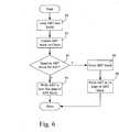
- step 50Shown in FIG. 4 is a procedure for writing to a free block of the flash memory.
- the proceduredetermines whether a free block is desired for writing. If not, then the procedure simply waits in step 50 .
- step 50determines that a free block is to be written
- the techniquereads the first element in the chain in step 52 and removes it from the list in step 54 .
- step 56The block with the block number indicated in the selected element is written to in step 56 and the procedure returns to step 50 to await the need for a new free block.
- Shown in FIG. 5is a procedure for controlling the erasing of blocks of the flash memory.
- the proceduredetects in step 60 when a block is erased and becomes free, reads the age of the block being erased from the Aging Block Table stored in the flash memory device (step 62 ), increments the age in step 64 , and a new Free Blocks Chain element is created in step 66 , with the age set to the age read, incremented by one unit.
- the element createdis subsequently inserted in the Free Block Chain in the right order in step 68 .
- step 70The procedure checks in step 70 whether the age of a block reaches the maximum storable value (65,535 in the exampled). If the maximum has not been reached, then the procedure simply returns to step 60 to await the erasure of another block of the flash memory. If step 70 determines that the maximum has been reached, then the following steps are executed:
- the Aging Block Table stored in the flash memory deviceis loaded in the RAM memory in step 72 ;
- the information items stored in the Free Block Chainare merged in the Aging Block Table stored in the RAM memory in step 74 ;
- the Aging Block Tableis rewritten in the flash memory device in step 78 , and subsequently the RAM memory is cleared.
- the procedurereturns to step 60 to await the erasure of another block of the flash memory.
- step 80it loads in the RAM memory the Aging Block Table stored in the flash memory device (step 80 ),
- step 84determines if the block containing the Aging Block Table has sufficient free pages to write the table from the RAM memory back to that block (step 84 ). If so, then it writes the table in the flash memory device starting from the first free page in step 86 . If not, it erases the block in step 88 and writes the ABT table from the RAM memory to the ABT block in step 90 , starting from the first page.
- the Aging Block Tablemaintains the right values for the ages of each block.
- FIG. 7 and the following discussionprovide a brief, general description of a suitable computing environment in which the invention may be implemented.
- at least one embodiment of the inventioncan be implemented in the general context of computer-executable instructions, such as program application modules, objects, or macros being executed by a personal computer.
- the inventioncan be practiced with other computing system configurations, including handheld devices, multiprocessor systems, microprocessor-based or programmable consumer electronics, network PCs, minicomputers, mainframe computers, and the like.
- the inventioncan be practiced in distributed computing environments where tasks or modules are performed by remote processing devices, which are linked through a communications network.
- program modulesmay be located in both local and remote memory storage devices.
- a personal computer referred to herein as a computing system 112includes a processing unit 113 , a system memory 114 and a system bus 116 that couples various system components including the system memory 114 to the processing unit 113 .
- the processing unit 113may be any logical processing unit, such as one or more central processing units (CPUs), digital signal processors (DSPs), application-specific integrated circuits (ASIC), etc. Unless described otherwise, the construction and operation of the various blocks shown in FIG. 7 are of conventional design. As a result, such blocks need not be described in further detail herein, as they will be understood by those skilled in the relevant art.
- the system bus 116can employ any known bus structures or architectures, including a memory bus with memory controller, a peripheral bus, and/or a local bus.
- the system memory 114includes read-only memory (“ROM”) 118 and random access memory (“RAM”) 120 .
- ROMread-only memory
- RAMrandom access memory
- a basic input/output system (“BIOS”) 122which can form part of the ROM 118 , contains basic routines that help transfer information between elements within the computing system 112 , such as during startup.
- the computing system 112also includes one or more spinning media memories such as a hard disk drive 124 for reading from and writing to a hard disk 125 , and an optical disk drive 126 and a magnetic disk drive 128 for reading from and writing to removable optical disks 130 and magnetic disks 132 , respectively.
- the optical disk 130can be a CD-ROM, while the magnetic disk 132 can be a magnetic floppy disk or diskette.
- the hard disk drive 124 , optical disk drive 126 and magnetic disk drive 128communicate with the processing unit 113 via the bus 116 .
- the hard disk drive 124 , optical disk drive 126 and magnetic disk drive 128may include interfaces or controllers coupled between such drives and the bus 116 , as is known by those skilled in the relevant art, for example via an IDE (i.e., Integrated Drive Electronics) interface.
- IDEi.e., Integrated Drive Electronics
- the drives 124 , 126 and 128 , and their associated computer-readable mediaprovide nonvolatile storage of computer-readable instructions, data structures, program modules and other data for the computing system 112 .
- the depicted computing system 112employs hard disk 125 , optical disk 130 and magnetic disk 132 , those skilled in the relevant art will appreciate that other types of spinning media memory computer-readable media may be employed, such as, digital video disks (“DVD”), Bernoulli cartridges, etc.
- Program modulescan be stored in the system memory 114 , such as an operating system 134 , one or more application programs 136 , other programs or modules 138 , and program data 140 .
- the system memory 14also includes a browser 141 for permitting the computing system 112 to access and exchange data with sources such as websites of the Internet, corporate intranets, or other networks, as well as other server applications on server computers.
- the browser 141is markup language based, such as hypertext markup language (“HTML”), and operate with markup languages that use syntactically delimited characters added to the data of a document to represent the structure of the document.
- HTMLhypertext markup language
- the operating system 134can be stored on the hard disk 125 of the hard disk drive 24 , the optical disk 130 and the optical disk drive 126 and/or the magnetic disk 132 of the magnetic disk drive 128 .
- a usercan enter commands and information to the computing system 112 through input devices such as a keyboard 142 and a pointing device such as a mouse 144 .
- Other input devicescan include a microphone, joystick, game pad, scanner, etc.
- a monitor 148 or other display devicesmay be coupled to the bus 116 via video interface 150 , such as a video adapter.
- the computing system 112can include other output devices such as speakers, printers, etc.
- the computing system 112can operate in a networked environment using logical connections to one or more remote computers.
- the computing system 112may employ any known means of communications, such as through a local area network (“LAN”) 152 or a wide area network (“WAN”) or the Internet 154 .
- LANlocal area network
- WANwide area network
- Such networking environmentsare well known in enterprise-wide computer networks, intranets, and the Internet.
- the computing system 112When used in a LAN networking environment, the computing system 112 is connected to the LAN 152 through an adapter or network interface 156 (communicatively linked to the bus 116 ). When used in a WAN networking environment, the computing system 112 often includes a modem 157 or other device for establishing communications over the WAN/Internet 154 .
- the modem 157is shown in FIG. 7 as communicatively linked between the interface 146 and the WAN/Internet 154 .
- program modules, application programs, or data, or portions thereofcan be stored in a server computer (not shown).
- server computernot shown.
- the computing system 112may include one or more interfaces to allow the addition of devices either internally or externally to the computing system 112 .
- suitable interfacesmay include ISA (i.e., Industry Standard Architecture), IDE, PCI (i.e., Personal Computer Interface) and/or AGP (i.e., Advance Graphics Processor) slot connectors for option cards, serial and/or parallel ports, USB ports (i.e., Universal Serial Bus), audio input/output (i.e., I/O) and MIDI/joystick connectors, and/or slots for memory.
- Non-volatile mediaincludes, for example, hard, optical or magnetic disks 125 , 130 , 132 , respectively.
- Volatile mediaincludes dynamic memory, such as system memory 114 .
- Transmission mediaincludes coaxial cables, copper wire and fiber optics, including the wires that comprise system bus 116 . Transmission media can also take the form of acoustic or light waves, such as those generated during radio wave and infrared data communications.
- Computer-readable mediainclude, for example, a floppy disk, a flexible disk, hard disk, magnetic tape, or any other magnetic medium, a CD-ROM, any other optical medium, punch cards, paper tape, any other physical medium with patterns of holes, a RAM, a PROM, and EPROM, a FLASH-EPROM, any other memory chip or cartridge, a carrier wave as described hereinafter, or any other medium from which a computer can read.
- Various forms of computer readable mediamay be involved in carrying one or more sequences of one or more instructions to processing unit 113 for execution.
- the instructionsmay initially be carried on a magnetic disk of a remote computer.
- the remote computercan load the instructions into its dynamic memory and send the instructions over a telephone line using a modem.
- the modem 157 local to computer system 112can receive the data on the telephone line and use an infrared transmitter to convert the data to an infrared signal.
- An infrared detector coupled to the system bus 116can receive the data carried in the infrared signal and place the data on system bus 116 .
- the system bus 116carries the data to system memory 114 , from which processing unit 113 retrieves and executes the instructions.
- the instructions received by system memory 114may optionally be stored on storage device either before or after execution by processing unit 113 .
- the computing systemalso includes a flash memory 158 that includes the AGT and is controlled according to the method discussed above with respect to FIGS. 2-6 .
- the instructions for implementing the methodcan also be stored in the flash memory 158 .
- the methodcould be implemented using the main processing unit 113 or a separate processor/controller that could be incorporated within the flash memory device or added to the computer system 112 and coupled to the bus 116 .
Landscapes
- Engineering & Computer Science (AREA)
- Theoretical Computer Science (AREA)
- Physics & Mathematics (AREA)
- General Engineering & Computer Science (AREA)
- General Physics & Mathematics (AREA)
- Techniques For Improving Reliability Of Storages (AREA)
Abstract
Description
- 1. Field of the Invention
- The invention relates to techniques for optimizing write/erase operations in memory/storage devices, and was developed by paying specific attention to the possible application in “flash” memories.
- 2. Description of the Related Art
- Flash memories are non-volatile storage devices, able to store recorded data without a power source. A computer program using the ability of a flash memory to be erased and reprogrammed can modify the data stored in a flash memory. These basic capabilities have made flash memories suitable for acting as standard storage media in computer systems, i.e. as flash disks.
- Flash devices are typically partitioned in several contiguous zones, each of which is individually erasable. Such zones are known under various designations, such as units or blocks. For the sake of clarity, in the following description they will be referred to as blocks or erase units.
- A limitation of flash memory technology lies in that the number of times a block can be erased is intrinsically limited by the physics of the flash cell. Repeated erasure of a block wears out the cells in the unit leading to a reduced capability to distinguish between the erased state and the programmed state. This results in a longer time being required to erase the unit, and to the appearance of sporadic faults in programming or erasing data. The unit may ultimately entirely lose its ability of being erased and reprogrammed.
- The effects of wear are statistical in nature, and the ability of a flash device to withstand wear is usually described in terms of a number called the program/erase endurance. This number is the minimum or average number of times each flash unit can be erased without encountering significant failures. Vendor endurance numbers currently range from tens of thousands to a million.
- The limited endurance limits the lifetime of a flash disk. It would be advantageous to have a lifetime that is as long as possible, and this depends on the pattern of access to the flash disk. Repeated and frequent writes to a single block or a small number of blocks will end the useful lifetime of the media quickly. On the other hand, if writes can be evenly distributed to all blocks of the media, each block will be capable of coming close to the maximum number of erases it can endure. The onset of failures will thus be delayed as much as possible, maximizing the lifetime of the media.
- Flash disk managers typically employ algorithms that give them discretion over the physical location where new data will be written, and they direct written data in such a way to guarantee that different flash units will be subjected to the same number of erases. Such a procedure is known in the art as “wear leveling”. Some managers record the number of erases a unit has experienced in a register in that unit, and enforce a procedure intended to guarantee that the variation in the number of erases of each unit will not exceed some small constant. Other arrangements use a randomization of the choice of the target unit, and rely on statistics and the law of large numbers to maintain an even wear across the flash media.
- While such prior art arrangements are capable of providing satisfactory results, the need is felt for improved solutions adapted to ensure a uniform use of each block in a flash memory. One embodiment of the present invention provides a fully satisfactory response to this need.
- One embodiment of the invention is directed to a method of controlling write/erase operations in a memory device including memory blocks that are exposed to wear as a result of repeated erasures. The method includes: storing erase counts of the memory blocks; creating a chain storing the erase counts of the memory blocks that are available for writing at a certain instant of time; and selecting for writing, out of the blocks of the memory device available for writing, the block having the lowest erase count in the chain.
- The invention will now be described, by way of example only, with reference to the enclosed drawings.
FIG. 1 shows an exemplary architecture of a flash memory that implements the arrangement described herein.FIG. 2 is a flowchart of a procedure for implementing an aged block table (ABT) when formatting the flash memory.FIG. 3 is a flowchart showing the creation of a free blocks chain used for a method according to one embodiment of the invention.FIG. 4 is a flowchart showing a write procedure according to one embodiment of the invention.FIG. 5 is a flowchart showing a procedure for updating an ABT and the free blocks chain in response to the erasure of a block of the flash memory, according to one embodiment of the invention.FIG. 6 is a flowchart showing a procedure for updating the ABT based on the free blocks chain.FIG. 7 is a block diagram of a computer system for implementing one embodiment of the present invention.- The solution described herein is essentially a technique for improving “wear leveling” of static areas in a flash memory, by ensuring a uniform use of each block in a flash memory device. This technique maintains the erase count of each block in a table and selects the block to write by choosing from the table the free block with the lowest erase count.
- Typically, the method comprises the steps of:
- storing in a table the erases count of each block in a flash memory, and
- creating a chain in a portion of a RAM memory (Random Access Memory) to store the erases count of the free blocks at a determined instant of time.
- As used herein, the term “chain” refers to a set of elements that are linked to one another either explicitly or implicitly. That is, the links between elements can be explicit in that one element includes a pointer that points to the next element. Alternatively, the links between elements can be implicit in that the elements are located in predetermined positions with respect to one another such that the next element is accessed automatically from a current element, such as in a table in which the next element is positioned immediately after or before the current element.
- The arrangement described herein ensures that when data are to be written in a free block, the block selected is the one that has been erased the minimum number of times.
- Specifically, the arrangement described herein provides for the following steps:
- storing the erases count of each block, named age, in a table, named Aging Block Table (ABT), memorized in the flash memory itself;
- keeping in the RAM memory a chain of information items related to the free blocks present in the flash device; and
- choosing for writing purposes, from the chain in the RAM memory, the block with the minimum number of erases cycle.
FIG. 1 shows a portion of a flash memory device that contains the Aging Block Table (ABT).- The i-th entry in the Aging Block Table represents the number of erase operations performed on the block of position—i—in the flash memory device. The number of erase operations for a given block is called the “age” of the block.
- In the example shown in
FIG. 1 the block is divided in a main area of 512 bytes and a spare area of 16 bytes. - The main area contains the entries of the Aging Block Table. The Aging Block Table contains an entry for each block in the flash memory device.
- In particular,
FIG. 1 shows an Aging Block Table for a flash device comprised of 4096 erasable blocks (each block is in turn comprised of 32 pages). - Each entry of the Aging Block Table is two bytes of size, so that each page contains 256 entries (1024 in devices with pages of 2048 bytes). Sixteen pages are used to store the Aging Block Table of the example shown in
FIG. 1 . - The pages used to store the Aging Block Table entries contain a flag, the Aging Block Table flag, in the fifth byte of the spare area.
- Shown in
FIG. 2 is a procedure for implementing the ABT when formatting the flash memory. First, in response to a format command, the procedure determines instep 10 whether it is the first format for the flash memory. If so, then the procedure searches instep 12 for the last non-defective block of the flash memory. The Aging Block Table is written in the last-non-defective block of the flash device instep 14 and the procedure finishes and awaits any subsequent formatting commands. - Initially, each age in the Aging Block Table is set to the value “one”. Entries related to “bad” blocks have their age set to the value “zero”.
- At power-on, the Aging Block Table is searched for starting from the last block in the flash memory device.
- The Aging Block Table is recognized by reading the spare area of the page. If, e.g., it contains the Aging Block Table flag in the fifth byte, the block contains the Aging Block Table.
- For each subsequent format operation as detected in
step 10 ofFIG. 2 , the ABT is not necessary erased. Instead, the procedure determines instep 16 whether there is enough space to update the ABT in the flash block in which the ABT is stored. - If there is enough free space in the same block to store the Aging Block Table, the Aging Block Table is updated in
step 18 by incrementing the ages of the blocks that will be erased in the format operation. - If
step 16 determines that no free space is available in the block, the Aging Block Table is loaded in the RAM memory instep 20, the block is completely erased instep 22, the ages for the erased blocks are incremented instep 24, and subsequently, the updated Aging Block Table (with new ages for erased blocks) is written in this block instep 26. - The solution described herein stores information about the free blocks of the flash memory device in a structure called Free Blocks Chain.
- The chain has an element for each free block in the flash memory device.
- For a given free block each element stores:
- the block number,
- the age of the block, and
- a pointer to the subsequent element in the chain.
- The chain is ordered in a FIFO (First In First Out) arrangement. When there is a limit on the dimensions of the RAM memory that can be used, the age of each block can be represented using two bytes. Therefore, up to 65,535 erase operations can be stored in each element.
- Since each block can be erased roughly 100,000 times, a technique to overcome this problem is proposed.
- The Free Block Chain is stored in a portion of the RAM memory and is reconstructed at every device power-on according to a procedure shown in
FIG. 3 in one embodiment. - In fact, at power-on, the spare area of the first page of each block in the flash memory device is read in
step 30. Every block has the third and fourth byte of the first spare indicating the state of the block (free or allocated), so it is possible to recognize the free blocks via the spare area instep 32. - If
step 32 determines that the block is not free, then instep 34 the method determines whether there are more blocks to read. If so, then the method returns to step30 to read the next block. If not, then the free blocks chain is ready to be used when it is desired to write to a new block as will be discussed in more detail below with respect toFIG. 4 . - During the read operation, for each block determined to be free in step32:
- the age is read from the Aging Block Table stored in the flash memory device in
step 36; - an element of the Free Blocks Chain is created with the block number and the age previously read in
step 38; and - the element created is inserted in the right order in the Free Block Chain in
step 40. - The method then returns to step34 to see if there are more blocks to read and the process is repeated as discussed above.
- Shown in
FIG. 4 is a procedure for writing to a free block of the flash memory. Instep 50, the procedure determines whether a free block is desired for writing. If not, then the procedure simply waits instep 50. - When
step 50 determines that a free block is to be written, the technique reads the first element in the chain instep 52 and removes it from the list instep 54. - The block with the block number indicated in the selected element is written to in
step 56 and the procedure returns to step50 to await the need for a new free block. - Shown in
FIG. 5 is a procedure for controlling the erasing of blocks of the flash memory. The procedure detects instep 60 when a block is erased and becomes free, reads the age of the block being erased from the Aging Block Table stored in the flash memory device (step62), increments the age instep 64, and a new Free Blocks Chain element is created instep 66, with the age set to the age read, incremented by one unit. The element created is subsequently inserted in the Free Block Chain in the right order instep 68. - As explained previously in the case of a RAM memory limitation of two bytes per element of the chain, a maximum of, e.g., 65,535 erase operations can be stored in each element of chain.
- The procedure checks in
step 70 whether the age of a block reaches the maximum storable value (65,535 in the exampled). If the maximum has not been reached, then the procedure simply returns to step60 to await the erasure of another block of the flash memory. Ifstep 70 determines that the maximum has been reached, then the following steps are executed: - the Aging Block Table stored in the flash memory device is loaded in the RAM memory in
step 72; - the information items stored in the Free Block Chain are merged in the Aging Block Table stored in the RAM memory in
step 74; - all the values of the Aging Block Table stored in the RAM memory are divided by two in
step 76; and - the Aging Block Table is rewritten in the flash memory device in
step 78, and subsequently the RAM memory is cleared. The procedure returns to step60 to await the erasure of another block of the flash memory. - After a set of erase operations performed on different blocks (e.g. after a “garbage collection” process) it is possible to merge the information stored in the Free Blocks Chain in the Aging Block Table stored in the RAM memory, thus updating the Aging Block Table.
- For this purpose the wear levelling technique operates in this manner as shown in
FIG. 6 : - it loads in the RAM memory the Aging Block Table stored in the flash memory device (step80),
- it updates in the RAM memory the entries related to the free blocks present in the Free Block Chain elements (step82), and
- determines if the block containing the Aging Block Table has sufficient free pages to write the table from the RAM memory back to that block (step84). If so, then it writes the table in the flash memory device starting from the first free page in
step 86. If not, it erases the block instep 88 and writes the ABT table from the RAM memory to the ABT block instep 90, starting from the first page. - In that way, the Aging Block Table maintains the right values for the ages of each block.
- Those skilled in the art will recognize that the method described above may be implemented in a general purpose computer system.
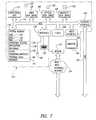
FIG. 7 and the following discussion provide a brief, general description of a suitable computing environment in which the invention may be implemented. Although not required, at least one embodiment of the invention can be implemented in the general context of computer-executable instructions, such as program application modules, objects, or macros being executed by a personal computer. Those skilled in the relevant art will appreciate that the invention can be practiced with other computing system configurations, including handheld devices, multiprocessor systems, microprocessor-based or programmable consumer electronics, network PCs, minicomputers, mainframe computers, and the like. The invention can be practiced in distributed computing environments where tasks or modules are performed by remote processing devices, which are linked through a communications network. In a distributed computing environment, program modules may be located in both local and remote memory storage devices. - Referring to
FIG. 7 , a personal computer referred to herein as acomputing system 112 includes aprocessing unit 113, asystem memory 114 and asystem bus 116 that couples various system components including thesystem memory 114 to theprocessing unit 113. Theprocessing unit 113 may be any logical processing unit, such as one or more central processing units (CPUs), digital signal processors (DSPs), application-specific integrated circuits (ASIC), etc. Unless described otherwise, the construction and operation of the various blocks shown inFIG. 7 are of conventional design. As a result, such blocks need not be described in further detail herein, as they will be understood by those skilled in the relevant art. - The
system bus 116 can employ any known bus structures or architectures, including a memory bus with memory controller, a peripheral bus, and/or a local bus. Thesystem memory 114 includes read-only memory (“ROM”)118 and random access memory (“RAM”)120. A basic input/output system (“BIOS”)122, which can form part of theROM 118, contains basic routines that help transfer information between elements within thecomputing system 112, such as during startup. - The
computing system 112 also includes one or more spinning media memories such as ahard disk drive 124 for reading from and writing to ahard disk 125, and anoptical disk drive 126 and amagnetic disk drive 128 for reading from and writing to removableoptical disks 130 andmagnetic disks 132, respectively. Theoptical disk 130 can be a CD-ROM, while themagnetic disk 132 can be a magnetic floppy disk or diskette. Thehard disk drive 124,optical disk drive 126 andmagnetic disk drive 128 communicate with theprocessing unit 113 via thebus 116. Thehard disk drive 124,optical disk drive 126 andmagnetic disk drive 128 may include interfaces or controllers coupled between such drives and thebus 116, as is known by those skilled in the relevant art, for example via an IDE (i.e., Integrated Drive Electronics) interface. Thedrives computing system 112. Although the depictedcomputing system 112 employshard disk 125,optical disk 130 andmagnetic disk 132, those skilled in the relevant art will appreciate that other types of spinning media memory computer-readable media may be employed, such as, digital video disks (“DVD”), Bernoulli cartridges, etc. - Program modules can be stored in the
system memory 114, such as anoperating system 134, one ormore application programs 136, other programs ormodules 138, andprogram data 140. Thesystem memory 14 also includes abrowser 141 for permitting thecomputing system 112 to access and exchange data with sources such as websites of the Internet, corporate intranets, or other networks, as well as other server applications on server computers. Thebrowser 141 is markup language based, such as hypertext markup language (“HTML”), and operate with markup languages that use syntactically delimited characters added to the data of a document to represent the structure of the document. - While shown in
FIG. 7 as being stored in the system memory, theoperating system 134,application programs 136,other program modules 138,program data 140 andbrowser 141 can be stored on thehard disk 125 of thehard disk drive 24, theoptical disk 130 and theoptical disk drive 126 and/or themagnetic disk 132 of themagnetic disk drive 128. A user can enter commands and information to thecomputing system 112 through input devices such as akeyboard 142 and a pointing device such as amouse 144. Other input devices can include a microphone, joystick, game pad, scanner, etc. These and other input devices are connected to theprocessing unit 113 through aninterface 146 such as a serial port interface that couples to thebus 116, although other interfaces such as a parallel port, a game port or a universal serial bus (“USB”) can be used. Amonitor 148 or other display devices may be coupled to thebus 116 viavideo interface 150, such as a video adapter. Thecomputing system 112 can include other output devices such as speakers, printers, etc. - The
computing system 112 can operate in a networked environment using logical connections to one or more remote computers. Thecomputing system 112 may employ any known means of communications, such as through a local area network (“LAN”)152 or a wide area network (“WAN”) or theInternet 154. Such networking environments are well known in enterprise-wide computer networks, intranets, and the Internet. - When used in a LAN networking environment, the
computing system 112 is connected to theLAN 152 through an adapter or network interface156 (communicatively linked to the bus116). When used in a WAN networking environment, thecomputing system 112 often includes amodem 157 or other device for establishing communications over the WAN/Internet 154. Themodem 157 is shown inFIG. 7 as communicatively linked between theinterface 146 and the WAN/Internet 154. In a networked environment, program modules, application programs, or data, or portions thereof, can be stored in a server computer (not shown). Those skilled in the relevant art will readily recognize that the network connections shown inFIG. 7 are only some examples of establishing communication links between computers, and other links may be used, including wireless links. - The
computing system 112 may include one or more interfaces to allow the addition of devices either internally or externally to thecomputing system 112. For example, suitable interfaces may include ISA (i.e., Industry Standard Architecture), IDE, PCI (i.e., Personal Computer Interface) and/or AGP (i.e., Advance Graphics Processor) slot connectors for option cards, serial and/or parallel ports, USB ports (i.e., Universal Serial Bus), audio input/output (i.e., I/O) and MIDI/joystick connectors, and/or slots for memory. - The term “computer-readable medium” as used herein refers to any medium that participates in providing instructions to
processing unit 113 for execution. Such a medium may take many forms, including but not limited to, non-volatile media, volatile media, and transmission media. Non-volatile media includes, for example, hard, optical ormagnetic disks system memory 114. Transmission media includes coaxial cables, copper wire and fiber optics, including the wires that comprisesystem bus 116. Transmission media can also take the form of acoustic or light waves, such as those generated during radio wave and infrared data communications. - Common forms of computer-readable media include, for example, a floppy disk, a flexible disk, hard disk, magnetic tape, or any other magnetic medium, a CD-ROM, any other optical medium, punch cards, paper tape, any other physical medium with patterns of holes, a RAM, a PROM, and EPROM, a FLASH-EPROM, any other memory chip or cartridge, a carrier wave as described hereinafter, or any other medium from which a computer can read.
- Various forms of computer readable media may be involved in carrying one or more sequences of one or more instructions to
processing unit 113 for execution. For example, the instructions may initially be carried on a magnetic disk of a remote computer. The remote computer can load the instructions into its dynamic memory and send the instructions over a telephone line using a modem. Themodem 157 local tocomputer system 112 can receive the data on the telephone line and use an infrared transmitter to convert the data to an infrared signal. An infrared detector coupled to thesystem bus 116 can receive the data carried in the infrared signal and place the data onsystem bus 116. Thesystem bus 116 carries the data tosystem memory 114, from whichprocessing unit 113 retrieves and executes the instructions. The instructions received bysystem memory 114 may optionally be stored on storage device either before or after execution by processingunit 113. - Specific to one embodiment of the present invention, the computing system also includes a
flash memory 158 that includes the AGT and is controlled according to the method discussed above with respect toFIGS. 2-6 . The instructions for implementing the method can also be stored in theflash memory 158. The method could be implemented using themain processing unit 113 or a separate processor/controller that could be incorporated within the flash memory device or added to thecomputer system 112 and coupled to thebus 116. - Consequently, without prejudice to the underlying principles of the invention, the details and the embodiments may vary, also appreciably, with reference to what has been described by way of example only, without departing from the scope of the invention as defined by the annexed claims.
Claims (31)
Priority Applications (1)
| Application Number | Priority Date | Filing Date | Title |
|---|---|---|---|
| US11/035,013US7363421B2 (en) | 2005-01-13 | 2005-01-13 | Optimizing write/erase operations in memory devices |
Applications Claiming Priority (1)
| Application Number | Priority Date | Filing Date | Title |
|---|---|---|---|
| US11/035,013US7363421B2 (en) | 2005-01-13 | 2005-01-13 | Optimizing write/erase operations in memory devices |
Publications (2)
| Publication Number | Publication Date |
|---|---|
| US20060155917A1true US20060155917A1 (en) | 2006-07-13 |
| US7363421B2 US7363421B2 (en) | 2008-04-22 |
Family
ID=36654601
Family Applications (1)
| Application Number | Title | Priority Date | Filing Date |
|---|---|---|---|
| US11/035,013Expired - LifetimeUS7363421B2 (en) | 2005-01-13 | 2005-01-13 | Optimizing write/erase operations in memory devices |
Country Status (1)
| Country | Link |
|---|---|
| US (1) | US7363421B2 (en) |
Cited By (48)
| Publication number | Priority date | Publication date | Assignee | Title |
|---|---|---|---|---|
| US20060265545A1 (en)* | 2005-05-20 | 2006-11-23 | Nec Infrontia Corporation | Information processing apparatus, lifetime monitoring method and program for monitoring lifetime of storage device including flash memory |
| US20070245100A1 (en)* | 2006-04-03 | 2007-10-18 | Fuji Xerox Co., Ltd. | Data processor, data processing method, and computer readable medium storing program therefor |
| US20070288685A1 (en)* | 2006-06-09 | 2007-12-13 | Phison Electronics Corp. | Flash memory scatter-write method |
| US20080112238A1 (en)* | 2006-10-25 | 2008-05-15 | Seon-Taek Kim | Hybrid flash memory device and method for assigning reserved blocks thereof |
| US20080282024A1 (en)* | 2007-05-09 | 2008-11-13 | Sudeep Biswas | Management of erase operations in storage devices based on flash memories |
| US20080282023A1 (en)* | 2007-05-09 | 2008-11-13 | Stmicroelectronics S.R.L. | Restoring storage devices based on flash memories and related circuit, system, and method |
| US20080282045A1 (en)* | 2007-05-09 | 2008-11-13 | Sudeep Biswas | Garbage collection in storage devices based on flash memories |
| US20080282025A1 (en)* | 2007-05-09 | 2008-11-13 | Stmicroelectronics S.R.L. | Wear leveling in storage devices based on flash memories and related circuit, system, and method |
| DE102007023408A1 (en)* | 2007-05-18 | 2008-11-20 | Mobotix Ag | Method for memory management |
| EP2000914A1 (en)* | 2007-06-08 | 2008-12-10 | Robert Bosch GmbH | Method and device for reorganising data in a storage system, in particular for control devices in motor vehicles |
| US20090193221A1 (en)* | 2008-01-29 | 2009-07-30 | Denali Software, Inc. | Method and apparatus for memory management in a non-volatile memory system using a block table |
| FR2935501A1 (en)* | 2008-09-02 | 2010-03-05 | Oberthur Technologies | Reinscribable non-volatile memory e.g. FLASH memory, access operation management method for e.g. subscriber identity module card, involves storing usage table in RAM or quick access storage |
| US20100115182A1 (en)* | 2008-11-06 | 2010-05-06 | Sony Corporation | Flash memory operation |
| US20100174845A1 (en)* | 2009-01-05 | 2010-07-08 | Sergey Anatolievich Gorobets | Wear Leveling for Non-Volatile Memories: Maintenance of Experience Count and Passive Techniques |
| US20100174846A1 (en)* | 2009-01-05 | 2010-07-08 | Alexander Paley | Nonvolatile Memory With Write Cache Having Flush/Eviction Methods |
| US20100287328A1 (en)* | 2009-05-07 | 2010-11-11 | Seagate Technology Llc | Wear leveling technique for storage devices |
| US20110087852A1 (en)* | 2008-06-17 | 2011-04-14 | Nxp B.V. | Method of and system for controlling the programming of memory devices |
| US20110219177A1 (en)* | 2008-04-24 | 2011-09-08 | Shinichi Kanno | Memory system and control method thereof |
| US20110271046A1 (en)* | 2008-10-28 | 2011-11-03 | Iyer Rahul N | Wear leveling for low-wear areas of low-latency random read memory |
| CN101236789B (en)* | 2006-12-18 | 2012-05-09 | 三星电子株式会社 | Method and apparatus for detecting static data area, wear-leveling, and merging data units |
| US8407449B1 (en) | 2010-02-26 | 2013-03-26 | Western Digital Technologies, Inc. | Non-volatile semiconductor memory storing an inverse map for rebuilding a translation table |
| US8521972B1 (en) | 2010-06-30 | 2013-08-27 | Western Digital Technologies, Inc. | System and method for optimizing garbage collection in data storage |
| US8725931B1 (en) | 2010-03-26 | 2014-05-13 | Western Digital Technologies, Inc. | System and method for managing the execution of memory commands in a solid-state memory |
| US8782327B1 (en) | 2010-05-11 | 2014-07-15 | Western Digital Technologies, Inc. | System and method for managing execution of internal commands and host commands in a solid-state memory |
| US8788778B1 (en) | 2012-06-04 | 2014-07-22 | Western Digital Technologies, Inc. | Garbage collection based on the inactivity level of stored data |
| US8819375B1 (en) | 2011-11-30 | 2014-08-26 | Western Digital Technologies, Inc. | Method for selective defragmentation in a data storage device |
| US20140281133A1 (en)* | 2013-03-15 | 2014-09-18 | Vijay Karamcheti | Managing the write performance of an asymmetric memory system |
| US8898548B1 (en) | 2012-08-24 | 2014-11-25 | Western Digital Technologies, Inc. | Methods, data storage devices and systems having variable size ECC page size |
| US20140379968A1 (en)* | 2010-09-24 | 2014-12-25 | Kabushiki Kaisha Toshiba | Memory system having a plurality of writing mode |
| US9021192B1 (en) | 2010-09-21 | 2015-04-28 | Western Digital Technologies, Inc. | System and method for enhancing processing of memory access requests |
| US9026716B2 (en) | 2010-05-12 | 2015-05-05 | Western Digital Technologies, Inc. | System and method for managing garbage collection in solid-state memory |
| US20150161040A1 (en)* | 2013-12-09 | 2015-06-11 | Silicon Motion, Inc. | Data-storage device and data erasing method |
| US9158670B1 (en) | 2011-06-30 | 2015-10-13 | Western Digital Technologies, Inc. | System and method for dynamically adjusting garbage collection policies in solid-state memory |
| US9164886B1 (en) | 2010-09-21 | 2015-10-20 | Western Digital Technologies, Inc. | System and method for multistage processing in a memory storage subsystem |
| US9189392B1 (en) | 2011-06-30 | 2015-11-17 | Western Digital Technologies, Inc. | Opportunistic defragmentation during garbage collection |
| US20160034386A1 (en)* | 2014-08-04 | 2016-02-04 | International Business Machines Corporation | Controlling wear among flash memory devices based on remaining warranty |
| US9268682B2 (en) | 2012-10-05 | 2016-02-23 | Skyera, Llc | Methods, devices and systems for physical-to-logical mapping in solid state drives |
| US9354955B1 (en) | 2014-03-19 | 2016-05-31 | Western Digital Technologies, Inc. | Partial garbage collection for fast error handling and optimized garbage collection for the invisible band |
| US9489296B1 (en) | 2012-10-17 | 2016-11-08 | Western Digital Technologies, Inc. | Methods, devices and systems for hardware-based garbage collection in solid state drives |
| US9507523B1 (en) | 2012-10-12 | 2016-11-29 | Western Digital Technologies, Inc. | Methods, devices and systems for variable size logical page management in a solid state drive |
| US9734027B2 (en) | 2013-03-15 | 2017-08-15 | Virident Systems, Llc | Synchronous mirroring in non-volatile memory systems |
| US9811285B1 (en) | 2012-12-28 | 2017-11-07 | Virident Systems, Llc | Dynamic restriping in nonvolatile memory systems |
| US9842660B1 (en) | 2012-12-28 | 2017-12-12 | Virident Systems, Llc | System and method to improve enterprise reliability through tracking I/O performance metrics in non-volatile random access memory |
| US9898196B1 (en) | 2013-03-15 | 2018-02-20 | Virident Systems, Llc | Small block write operations in non-volatile memory systems |
| US10884889B2 (en) | 2018-06-22 | 2021-01-05 | Seagate Technology Llc | Allocating part of a raid stripe to repair a second raid stripe |
| CN114005476A (en)* | 2021-10-29 | 2022-02-01 | 锐凌无线通讯科技(深圳)有限公司 | Flash memory, flash memory erasing and writing counting method, electronic equipment and computer storage medium |
| CN115221072A (en)* | 2021-04-21 | 2022-10-21 | 建兴储存科技股份有限公司 | Flash translation layer mapping table processing method of solid-state storage device |
| CN115909538A (en)* | 2021-09-30 | 2023-04-04 | 欧温阿尔法股份有限公司 | Vehicle data collection system and method of use thereof |
Families Citing this family (8)
| Publication number | Priority date | Publication date | Assignee | Title |
|---|---|---|---|---|
| US7865761B1 (en) | 2007-06-28 | 2011-01-04 | Emc Corporation | Accessing multiple non-volatile semiconductor memory modules in an uneven manner |
| JP5171448B2 (en)* | 2007-07-31 | 2013-03-27 | キヤノン株式会社 | Image forming apparatus and control method thereof |
| US8554983B2 (en) | 2008-05-27 | 2013-10-08 | Micron Technology, Inc. | Devices and methods for operating a solid state drive |
| US7719876B2 (en) | 2008-07-31 | 2010-05-18 | Unity Semiconductor Corporation | Preservation circuit and methods to maintain values representing data in one or more layers of memory |
| US8094500B2 (en) | 2009-01-05 | 2012-01-10 | Sandisk Technologies Inc. | Non-volatile memory and method with write cache partitioning |
| US8244960B2 (en)* | 2009-01-05 | 2012-08-14 | Sandisk Technologies Inc. | Non-volatile memory and method with write cache partition management methods |
| US20100318719A1 (en)* | 2009-06-12 | 2010-12-16 | Micron Technology, Inc. | Methods, memory controllers and devices for wear leveling a memory |
| CN102279712A (en)* | 2011-08-10 | 2011-12-14 | 北京百度网讯科技有限公司 | Storage control method, system and device applied to network storage system |
Citations (12)
| Publication number | Priority date | Publication date | Assignee | Title |
|---|---|---|---|---|
| US5568423A (en)* | 1995-04-14 | 1996-10-22 | Unisys Corporation | Flash memory wear leveling system providing immediate direct access to microprocessor |
| US6000006A (en)* | 1997-08-25 | 1999-12-07 | Bit Microsystems, Inc. | Unified re-map and cache-index table with dual write-counters for wear-leveling of non-volatile flash RAM mass storage |
| US6081447A (en)* | 1991-09-13 | 2000-06-27 | Western Digital Corporation | Wear leveling techniques for flash EEPROM systems |
| US6092160A (en)* | 1996-09-30 | 2000-07-18 | Nokia Mobile Phones Limited | Memory management method |
| US6426893B1 (en)* | 2000-02-17 | 2002-07-30 | Sandisk Corporation | Flash eeprom system with simultaneous multiple data sector programming and storage of physical block characteristics in other designated blocks |
| US6621746B1 (en)* | 2002-02-27 | 2003-09-16 | Microsoft Corporation | Monitoring entropic conditions of a flash memory device as an indicator for invoking erasure operations |
| US20030225961A1 (en)* | 2002-06-03 | 2003-12-04 | James Chow | Flash memory management system and method |
| US20040088474A1 (en)* | 2002-10-30 | 2004-05-06 | Lin Jin Shin | NAND type flash memory disk device and method for detecting the logical address |
| US20040177212A1 (en)* | 2002-10-28 | 2004-09-09 | Sandisk Corporation | Maintaining an average erase count in a non-volatile storage system |
| US20050071403A1 (en)* | 2003-09-29 | 2005-03-31 | Broadcom Corporation | Method, system, and computer program product for executing SIMD instruction for flexible FFT butterfly |
| US6925012B2 (en)* | 1991-11-26 | 2005-08-02 | Renesas Technology Corp. | Storage device employing a flash memory |
| US7093161B1 (en)* | 2002-08-16 | 2006-08-15 | Onspec Electronic, Inc. | Software recovery method for flash media with defective formatting |
- 2005
- 2005-01-13USUS11/035,013patent/US7363421B2/ennot_activeExpired - Lifetime
Patent Citations (12)
| Publication number | Priority date | Publication date | Assignee | Title |
|---|---|---|---|---|
| US6081447A (en)* | 1991-09-13 | 2000-06-27 | Western Digital Corporation | Wear leveling techniques for flash EEPROM systems |
| US6925012B2 (en)* | 1991-11-26 | 2005-08-02 | Renesas Technology Corp. | Storage device employing a flash memory |
| US5568423A (en)* | 1995-04-14 | 1996-10-22 | Unisys Corporation | Flash memory wear leveling system providing immediate direct access to microprocessor |
| US6092160A (en)* | 1996-09-30 | 2000-07-18 | Nokia Mobile Phones Limited | Memory management method |
| US6000006A (en)* | 1997-08-25 | 1999-12-07 | Bit Microsystems, Inc. | Unified re-map and cache-index table with dual write-counters for wear-leveling of non-volatile flash RAM mass storage |
| US6426893B1 (en)* | 2000-02-17 | 2002-07-30 | Sandisk Corporation | Flash eeprom system with simultaneous multiple data sector programming and storage of physical block characteristics in other designated blocks |
| US6621746B1 (en)* | 2002-02-27 | 2003-09-16 | Microsoft Corporation | Monitoring entropic conditions of a flash memory device as an indicator for invoking erasure operations |
| US20030225961A1 (en)* | 2002-06-03 | 2003-12-04 | James Chow | Flash memory management system and method |
| US7093161B1 (en)* | 2002-08-16 | 2006-08-15 | Onspec Electronic, Inc. | Software recovery method for flash media with defective formatting |
| US20040177212A1 (en)* | 2002-10-28 | 2004-09-09 | Sandisk Corporation | Maintaining an average erase count in a non-volatile storage system |
| US20040088474A1 (en)* | 2002-10-30 | 2004-05-06 | Lin Jin Shin | NAND type flash memory disk device and method for detecting the logical address |
| US20050071403A1 (en)* | 2003-09-29 | 2005-03-31 | Broadcom Corporation | Method, system, and computer program product for executing SIMD instruction for flexible FFT butterfly |
Cited By (93)
| Publication number | Priority date | Publication date | Assignee | Title |
|---|---|---|---|---|
| US20060265545A1 (en)* | 2005-05-20 | 2006-11-23 | Nec Infrontia Corporation | Information processing apparatus, lifetime monitoring method and program for monitoring lifetime of storage device including flash memory |
| US7904637B2 (en)* | 2005-05-20 | 2011-03-08 | Nec Infrontia Corporation | Information processing apparatus, lifetime monitoring method and program for monitoring lifetime of storage device including flash memory |
| US20070245100A1 (en)* | 2006-04-03 | 2007-10-18 | Fuji Xerox Co., Ltd. | Data processor, data processing method, and computer readable medium storing program therefor |
| US7886107B2 (en)* | 2006-04-03 | 2011-02-08 | Fuji Xerox Co., Ltd. | Data processor, data processing method, and computer readable medium storing program therefor |
| US20070288685A1 (en)* | 2006-06-09 | 2007-12-13 | Phison Electronics Corp. | Flash memory scatter-write method |
| US7453712B2 (en)* | 2006-10-25 | 2008-11-18 | Samsung Electronics Co., Ltd. | Hybrid flash memory device and method for assigning reserved blocks thereof |
| US20080112238A1 (en)* | 2006-10-25 | 2008-05-15 | Seon-Taek Kim | Hybrid flash memory device and method for assigning reserved blocks thereof |
| CN101236789B (en)* | 2006-12-18 | 2012-05-09 | 三星电子株式会社 | Method and apparatus for detecting static data area, wear-leveling, and merging data units |
| US8954649B2 (en) | 2007-05-09 | 2015-02-10 | SK Hynix Inc. | Garbage collection in storage devices based on flash memories |
| US20080282045A1 (en)* | 2007-05-09 | 2008-11-13 | Sudeep Biswas | Garbage collection in storage devices based on flash memories |
| US7991942B2 (en) | 2007-05-09 | 2011-08-02 | Stmicroelectronics S.R.L. | Memory block compaction method, circuit, and system in storage devices based on flash memories |
| US8099545B2 (en) | 2007-05-09 | 2012-01-17 | Stmicroelectronics S.R.L. | Wear leveling in storage devices based on flash memories and related circuit, system, and method |
| US20080282023A1 (en)* | 2007-05-09 | 2008-11-13 | Stmicroelectronics S.R.L. | Restoring storage devices based on flash memories and related circuit, system, and method |
| US8041883B2 (en) | 2007-05-09 | 2011-10-18 | Stmicroelectronics S.R.L. | Restoring storage devices based on flash memories and related circuit, system, and method |
| US20110087832A1 (en)* | 2007-05-09 | 2011-04-14 | Stmicroelectronics, S.R.L. | Wear leveling in storage devices based on flash memories and related circuit, system, and method |
| US20080282024A1 (en)* | 2007-05-09 | 2008-11-13 | Sudeep Biswas | Management of erase operations in storage devices based on flash memories |
| US9146854B2 (en) | 2007-05-09 | 2015-09-29 | Stmicroelectronics International N.V. | Restoring storage devices based on flash memories and related circuit, system, and method |
| US7882301B2 (en) | 2007-05-09 | 2011-02-01 | Stmicroelectronics S.R.L. | Wear leveling in storage devices based on flash memories and related circuit, system, and method |
| US20080282025A1 (en)* | 2007-05-09 | 2008-11-13 | Stmicroelectronics S.R.L. | Wear leveling in storage devices based on flash memories and related circuit, system, and method |
| WO2008141616A1 (en) | 2007-05-18 | 2008-11-27 | Mobotix Ag | Method for memory management |
| DE102007023408A1 (en)* | 2007-05-18 | 2008-11-20 | Mobotix Ag | Method for memory management |
| US20080307153A1 (en)* | 2007-06-08 | 2008-12-11 | Joern Boettcher | Method and device for reorganizing data in a memory system, in particular for control devices in motor vehicles |
| US8010737B2 (en) | 2007-06-08 | 2011-08-30 | Robert Bosch Gmbh | Method and device for reorganizing data in a memory system, in particular for control devices in motor vehicles |
| EP2000914A1 (en)* | 2007-06-08 | 2008-12-10 | Robert Bosch GmbH | Method and device for reorganising data in a storage system, in particular for control devices in motor vehicles |
| US7945762B2 (en)* | 2008-01-29 | 2011-05-17 | Cadence Design Systems, Inc. | Method and apparatus for memory management in a non-volatile memory system using a block table |
| US20090193221A1 (en)* | 2008-01-29 | 2009-07-30 | Denali Software, Inc. | Method and apparatus for memory management in a non-volatile memory system using a block table |
| US20110219177A1 (en)* | 2008-04-24 | 2011-09-08 | Shinichi Kanno | Memory system and control method thereof |
| US20110087852A1 (en)* | 2008-06-17 | 2011-04-14 | Nxp B.V. | Method of and system for controlling the programming of memory devices |
| US8631218B2 (en) | 2008-06-17 | 2014-01-14 | Nxp, B.V. | Method of and system for controlling the programming of memory devices |
| FR2935501A1 (en)* | 2008-09-02 | 2010-03-05 | Oberthur Technologies | Reinscribable non-volatile memory e.g. FLASH memory, access operation management method for e.g. subscriber identity module card, involves storing usage table in RAM or quick access storage |
| US20110271046A1 (en)* | 2008-10-28 | 2011-11-03 | Iyer Rahul N | Wear leveling for low-wear areas of low-latency random read memory |
| US8495284B2 (en)* | 2008-10-28 | 2013-07-23 | Netapp, Inc. | Wear leveling for low-wear areas of low-latency random read memory |
| US20100115182A1 (en)* | 2008-11-06 | 2010-05-06 | Sony Corporation | Flash memory operation |
| US8700840B2 (en) | 2009-01-05 | 2014-04-15 | SanDisk Technologies, Inc. | Nonvolatile memory with write cache having flush/eviction methods |
| US20120191927A1 (en)* | 2009-01-05 | 2012-07-26 | Sergey Anatolievich Gorobets | Wear Leveling for Non-Volatile Memories: Maintenance of Experience Count and Passive Techniques |
| US20100174846A1 (en)* | 2009-01-05 | 2010-07-08 | Alexander Paley | Nonvolatile Memory With Write Cache Having Flush/Eviction Methods |
| US20100174845A1 (en)* | 2009-01-05 | 2010-07-08 | Sergey Anatolievich Gorobets | Wear Leveling for Non-Volatile Memories: Maintenance of Experience Count and Passive Techniques |
| US8051241B2 (en) | 2009-05-07 | 2011-11-01 | Seagate Technology Llc | Wear leveling technique for storage devices |
| US8301830B2 (en) | 2009-05-07 | 2012-10-30 | Seagate Technology Llc | Wear leveling technique for storage devices |
| US20100287328A1 (en)* | 2009-05-07 | 2010-11-11 | Seagate Technology Llc | Wear leveling technique for storage devices |
| US8407449B1 (en) | 2010-02-26 | 2013-03-26 | Western Digital Technologies, Inc. | Non-volatile semiconductor memory storing an inverse map for rebuilding a translation table |
| US8489854B1 (en) | 2010-02-26 | 2013-07-16 | Western Digital Technologies, Inc. | Non-volatile semiconductor memory storing an inverse map for rebuilding a translation table |
| US8725931B1 (en) | 2010-03-26 | 2014-05-13 | Western Digital Technologies, Inc. | System and method for managing the execution of memory commands in a solid-state memory |
| US8782327B1 (en) | 2010-05-11 | 2014-07-15 | Western Digital Technologies, Inc. | System and method for managing execution of internal commands and host commands in a solid-state memory |
| US9405675B1 (en) | 2010-05-11 | 2016-08-02 | Western Digital Technologies, Inc. | System and method for managing execution of internal commands and host commands in a solid-state memory |
| US9026716B2 (en) | 2010-05-12 | 2015-05-05 | Western Digital Technologies, Inc. | System and method for managing garbage collection in solid-state memory |
| US8706985B1 (en) | 2010-06-30 | 2014-04-22 | Western Digital Technologies, Inc. | System and method for optimizing garbage collection in data storage |
| US8521972B1 (en) | 2010-06-30 | 2013-08-27 | Western Digital Technologies, Inc. | System and method for optimizing garbage collection in data storage |
| US10048875B2 (en) | 2010-09-21 | 2018-08-14 | Western Digital Technologies, Inc. | System and method for managing access requests to a memory storage subsystem |
| US9164886B1 (en) | 2010-09-21 | 2015-10-20 | Western Digital Technologies, Inc. | System and method for multistage processing in a memory storage subsystem |
| US9477413B2 (en) | 2010-09-21 | 2016-10-25 | Western Digital Technologies, Inc. | System and method for managing access requests to a memory storage subsystem |
| US9021192B1 (en) | 2010-09-21 | 2015-04-28 | Western Digital Technologies, Inc. | System and method for enhancing processing of memory access requests |
| US12265706B2 (en) | 2010-09-24 | 2025-04-01 | Kioxia Corporation | Memory system with nonvolatile semiconductor memory |
| US11893238B2 (en) | 2010-09-24 | 2024-02-06 | Kioxia Corporation | Method of controlling nonvolatile semiconductor memory |
| US20140379968A1 (en)* | 2010-09-24 | 2014-12-25 | Kabushiki Kaisha Toshiba | Memory system having a plurality of writing mode |
| US11579773B2 (en) | 2010-09-24 | 2023-02-14 | Toshiba Memory Corporation | Memory system and method of controlling memory system |
| US11216185B2 (en) | 2010-09-24 | 2022-01-04 | Toshiba Memory Corporation | Memory system and method of controlling memory system |
| US10877664B2 (en)* | 2010-09-24 | 2020-12-29 | Toshiba Memory Corporation | Memory system having a plurality of writing modes |
| US10871900B2 (en) | 2010-09-24 | 2020-12-22 | Toshiba Memory Corporation | Memory system and method of controlling memory system |
| US9158670B1 (en) | 2011-06-30 | 2015-10-13 | Western Digital Technologies, Inc. | System and method for dynamically adjusting garbage collection policies in solid-state memory |
| US9189392B1 (en) | 2011-06-30 | 2015-11-17 | Western Digital Technologies, Inc. | Opportunistic defragmentation during garbage collection |
| US9678671B2 (en) | 2011-06-30 | 2017-06-13 | Western Digital Technologies, Inc. | System and method for dynamically adjusting garbage collection policies in solid-state memory |
| US8819375B1 (en) | 2011-11-30 | 2014-08-26 | Western Digital Technologies, Inc. | Method for selective defragmentation in a data storage device |
| US8788778B1 (en) | 2012-06-04 | 2014-07-22 | Western Digital Technologies, Inc. | Garbage collection based on the inactivity level of stored data |
| US8898548B1 (en) | 2012-08-24 | 2014-11-25 | Western Digital Technologies, Inc. | Methods, data storage devices and systems having variable size ECC page size |
| US9268682B2 (en) | 2012-10-05 | 2016-02-23 | Skyera, Llc | Methods, devices and systems for physical-to-logical mapping in solid state drives |
| US9507523B1 (en) | 2012-10-12 | 2016-11-29 | Western Digital Technologies, Inc. | Methods, devices and systems for variable size logical page management in a solid state drive |
| US9489296B1 (en) | 2012-10-17 | 2016-11-08 | Western Digital Technologies, Inc. | Methods, devices and systems for hardware-based garbage collection in solid state drives |
| US10055345B2 (en) | 2012-10-17 | 2018-08-21 | Western Digital Technologies, Inc. | Methods, devices and systems for solid state drive control |
| US9811285B1 (en) | 2012-12-28 | 2017-11-07 | Virident Systems, Llc | Dynamic restriping in nonvolatile memory systems |
| US9842660B1 (en) | 2012-12-28 | 2017-12-12 | Virident Systems, Llc | System and method to improve enterprise reliability through tracking I/O performance metrics in non-volatile random access memory |
| US9898196B1 (en) | 2013-03-15 | 2018-02-20 | Virident Systems, Llc | Small block write operations in non-volatile memory systems |
| US9734027B2 (en) | 2013-03-15 | 2017-08-15 | Virident Systems, Llc | Synchronous mirroring in non-volatile memory systems |
| US9164891B2 (en) | 2013-03-15 | 2015-10-20 | Virident Systems Inc. | Managing the write performance of an asymmetric memory system |
| US9733840B2 (en) | 2013-03-15 | 2017-08-15 | Virident Systems, Llc | Managing the write performance of an asymmetric memory system |
| US10073626B2 (en)* | 2013-03-15 | 2018-09-11 | Virident Systems, Llc | Managing the write performance of an asymmetric memory system |
| US9477595B2 (en) | 2013-03-15 | 2016-10-25 | Virident Systems Inc. | Managing the write performance of an asymmetric memory system |
| US9323663B2 (en) | 2013-03-15 | 2016-04-26 | Virident Systems Inc. | Managing the write performance of an asymmetric memory system |
| US9588698B1 (en) | 2013-03-15 | 2017-03-07 | Virident Systems Inc. | Managing the write performance of an asymmetric memory system |
| US20140281133A1 (en)* | 2013-03-15 | 2014-09-18 | Vijay Karamcheti | Managing the write performance of an asymmetric memory system |
| US10475516B2 (en)* | 2013-12-09 | 2019-11-12 | Silicon Motion, Inc. | Data storage device and data erasing method wherein after erasing process, predetermined value is written to indicate completion of said erasing method |
| US20150161040A1 (en)* | 2013-12-09 | 2015-06-11 | Silicon Motion, Inc. | Data-storage device and data erasing method |
| US9354955B1 (en) | 2014-03-19 | 2016-05-31 | Western Digital Technologies, Inc. | Partial garbage collection for fast error handling and optimized garbage collection for the invisible band |
| US10061696B2 (en) | 2014-03-19 | 2018-08-28 | Western Digital Technologies, Inc. | Partial garbage collection for fast error handling and optimized garbage collection for the invisible band |
| US10528461B2 (en)* | 2014-08-04 | 2020-01-07 | Lenovo Enterprise Solutions (Singapore) Pte. Ltd. | Controlling wear among flash memory devices based on remaining warranty |
| US20160034386A1 (en)* | 2014-08-04 | 2016-02-04 | International Business Machines Corporation | Controlling wear among flash memory devices based on remaining warranty |
| US10884889B2 (en) | 2018-06-22 | 2021-01-05 | Seagate Technology Llc | Allocating part of a raid stripe to repair a second raid stripe |
| CN115221072A (en)* | 2021-04-21 | 2022-10-21 | 建兴储存科技股份有限公司 | Flash translation layer mapping table processing method of solid-state storage device |
| US20220342545A1 (en)* | 2021-04-21 | 2022-10-27 | Solid State Storage Technology Corporation | Flash translation layer table processing method for solid state drive |
| US11487429B1 (en)* | 2021-04-21 | 2022-11-01 | Solid State Storage Technology Corporation | Flash translation layer table processing method for solid state drive |
| CN115909538A (en)* | 2021-09-30 | 2023-04-04 | 欧温阿尔法股份有限公司 | Vehicle data collection system and method of use thereof |
| CN114005476A (en)* | 2021-10-29 | 2022-02-01 | 锐凌无线通讯科技(深圳)有限公司 | Flash memory, flash memory erasing and writing counting method, electronic equipment and computer storage medium |
| WO2023070842A1 (en)* | 2021-10-29 | 2023-05-04 | 锐凌无线有限责任公司 | Flash memory, flash memory erase/write counting method, electronic device, and computer storage medium |
Also Published As
| Publication number | Publication date |
|---|---|
| US7363421B2 (en) | 2008-04-22 |
Similar Documents
| Publication | Publication Date | Title |
|---|---|---|
| US7363421B2 (en) | Optimizing write/erase operations in memory devices | |
| EP1739683B1 (en) | Space management for managing high capacity nonvolatile memory | |
| US7509474B2 (en) | Robust index storage for non-volatile memory | |
| US7663933B2 (en) | Memory controller | |
| EP1729304B1 (en) | Space management for managing high capacity nonvolatile memory | |
| US10168940B2 (en) | Data storage using SLC and TLC memory banks and data maintenance method thereof | |
| US20170336992A1 (en) | Method, device, and program for managing a flash memory for mass storage | |
| US10475516B2 (en) | Data storage device and data erasing method wherein after erasing process, predetermined value is written to indicate completion of said erasing method | |
| US7457909B2 (en) | Controlling operation of flash memories | |
| US10997073B2 (en) | Memory system | |
| US10168951B2 (en) | Methods for accessing data in a circular block mode and apparatuses using the same | |
| US20170285953A1 (en) | Data Storage Device and Data Maintenance Method thereof | |
| US7809878B2 (en) | Apparatus and method for controlling flash memory | |
| US9870826B2 (en) | Memory apparatus and data access method thereof by using multiple memories for lifetime extension | |
| US6510083B1 (en) | Electrically erasable and programmable memory that allows data update without prior erasure of the memory | |
| KR20030036133A (en) | A method and apparatus for reducing ram size while maintaining fast data access | |
| JP2003058417A (en) | Storage device | |
| US6898680B2 (en) | Minimization of overhead of non-volatile memory operation | |
| US20090055574A1 (en) | NAND Flash Memory Device And Related Method Thereof | |
| JP2000243093A (en) | Data storing method for flash memory and data reading out method from flash memory | |
| KR20250008277A (en) | Memory controller and memory system including the same | |
| CN101364438A (en) | Access device and method for improving NAND gate array flash memory | |
| JP2007219590A (en) | Information processor and its data erase method |
Legal Events
| Date | Code | Title | Description |
|---|---|---|---|
| AS | Assignment | Owner name:STMICROELECTRONICS S.R.L., ITALY Free format text:ASSIGNMENT OF ASSIGNORS INTEREST;ASSIGNORS:DI SENA, ANGELO;INTINI, AGATA;REEL/FRAME:019021/0093;SIGNING DATES FROM 20050405 TO 20050612 | |
| FEPP | Fee payment procedure | Free format text:PAYOR NUMBER ASSIGNED (ORIGINAL EVENT CODE: ASPN); ENTITY STATUS OF PATENT OWNER: LARGE ENTITY | |
| STCF | Information on status: patent grant | Free format text:PATENTED CASE | |
| FPAY | Fee payment | Year of fee payment:4 | |
| FEPP | Fee payment procedure | Free format text:PAYOR NUMBER ASSIGNED (ORIGINAL EVENT CODE: ASPN); ENTITY STATUS OF PATENT OWNER: LARGE ENTITY Free format text:PAYER NUMBER DE-ASSIGNED (ORIGINAL EVENT CODE: RMPN); ENTITY STATUS OF PATENT OWNER: LARGE ENTITY | |
| AS | Assignment | Owner name:MICRON TECHNOLOGY, INC., IDAHO Free format text:ASSIGNMENT OF ASSIGNORS INTEREST;ASSIGNOR:STMICROELECTRONICS S.R.L., (FORMERLY KNOWN AS SGS-THOMSON MICROELECTRONICS S.R.L.);REEL/FRAME:028888/0521 Effective date:20120523 | |
| FPAY | Fee payment | Year of fee payment:8 | |
| AS | Assignment | Owner name:U.S. BANK NATIONAL ASSOCIATION, AS COLLATERAL AGENT, CALIFORNIA Free format text:SECURITY INTEREST;ASSIGNOR:MICRON TECHNOLOGY, INC.;REEL/FRAME:038669/0001 Effective date:20160426 Owner name:U.S. BANK NATIONAL ASSOCIATION, AS COLLATERAL AGEN Free format text:SECURITY INTEREST;ASSIGNOR:MICRON TECHNOLOGY, INC.;REEL/FRAME:038669/0001 Effective date:20160426 | |
| AS | Assignment | Owner name:MORGAN STANLEY SENIOR FUNDING, INC., AS COLLATERAL AGENT, MARYLAND Free format text:PATENT SECURITY AGREEMENT;ASSIGNOR:MICRON TECHNOLOGY, INC.;REEL/FRAME:038954/0001 Effective date:20160426 Owner name:MORGAN STANLEY SENIOR FUNDING, INC., AS COLLATERAL Free format text:PATENT SECURITY AGREEMENT;ASSIGNOR:MICRON TECHNOLOGY, INC.;REEL/FRAME:038954/0001 Effective date:20160426 | |
| AS | Assignment | Owner name:U.S. BANK NATIONAL ASSOCIATION, AS COLLATERAL AGENT, CALIFORNIA Free format text:CORRECTIVE ASSIGNMENT TO CORRECT THE REPLACE ERRONEOUSLY FILED PATENT #7358718 WITH THE CORRECT PATENT #7358178 PREVIOUSLY RECORDED ON REEL 038669 FRAME 0001. ASSIGNOR(S) HEREBY CONFIRMS THE SECURITY INTEREST;ASSIGNOR:MICRON TECHNOLOGY, INC.;REEL/FRAME:043079/0001 Effective date:20160426 Owner name:U.S. BANK NATIONAL ASSOCIATION, AS COLLATERAL AGEN Free format text:CORRECTIVE ASSIGNMENT TO CORRECT THE REPLACE ERRONEOUSLY FILED PATENT #7358718 WITH THE CORRECT PATENT #7358178 PREVIOUSLY RECORDED ON REEL 038669 FRAME 0001. ASSIGNOR(S) HEREBY CONFIRMS THE SECURITY INTEREST;ASSIGNOR:MICRON TECHNOLOGY, INC.;REEL/FRAME:043079/0001 Effective date:20160426 | |
| AS | Assignment | Owner name:JPMORGAN CHASE BANK, N.A., AS COLLATERAL AGENT, ILLINOIS Free format text:SECURITY INTEREST;ASSIGNORS:MICRON TECHNOLOGY, INC.;MICRON SEMICONDUCTOR PRODUCTS, INC.;REEL/FRAME:047540/0001 Effective date:20180703 Owner name:JPMORGAN CHASE BANK, N.A., AS COLLATERAL AGENT, IL Free format text:SECURITY INTEREST;ASSIGNORS:MICRON TECHNOLOGY, INC.;MICRON SEMICONDUCTOR PRODUCTS, INC.;REEL/FRAME:047540/0001 Effective date:20180703 | |
| AS | Assignment | Owner name:MICRON TECHNOLOGY, INC., IDAHO Free format text:RELEASE BY SECURED PARTY;ASSIGNOR:U.S. BANK NATIONAL ASSOCIATION, AS COLLATERAL AGENT;REEL/FRAME:047243/0001 Effective date:20180629 | |
| AS | Assignment | Owner name:MICRON TECHNOLOGY, INC., IDAHO Free format text:RELEASE BY SECURED PARTY;ASSIGNOR:MORGAN STANLEY SENIOR FUNDING, INC., AS COLLATERAL AGENT;REEL/FRAME:050937/0001 Effective date:20190731 | |
| MAFP | Maintenance fee payment | Free format text:PAYMENT OF MAINTENANCE FEE, 12TH YEAR, LARGE ENTITY (ORIGINAL EVENT CODE: M1553); ENTITY STATUS OF PATENT OWNER: LARGE ENTITY Year of fee payment:12 | |
| AS | Assignment | Owner name:MICRON SEMICONDUCTOR PRODUCTS, INC., IDAHO Free format text:RELEASE BY SECURED PARTY;ASSIGNOR:JPMORGAN CHASE BANK, N.A., AS COLLATERAL AGENT;REEL/FRAME:051028/0001 Effective date:20190731 Owner name:MICRON TECHNOLOGY, INC., IDAHO Free format text:RELEASE BY SECURED PARTY;ASSIGNOR:JPMORGAN CHASE BANK, N.A., AS COLLATERAL AGENT;REEL/FRAME:051028/0001 Effective date:20190731 |