US20060151114A1 - Plasma processing system and baffle assembly for use in plasma processing system - Google Patents
Plasma processing system and baffle assembly for use in plasma processing systemDownload PDFInfo
- Publication number
- US20060151114A1 US20060151114A1US11/032,101US3210105AUS2006151114A1US 20060151114 A1US20060151114 A1US 20060151114A1US 3210105 AUS3210105 AUS 3210105AUS 2006151114 A1US2006151114 A1US 2006151114A1
- Authority
- US
- United States
- Prior art keywords
- baffle
- plasma processing
- processing system
- inserts
- carrier
- Prior art date
- Legal status (The legal status is an assumption and is not a legal conclusion. Google has not performed a legal analysis and makes no representation as to the accuracy of the status listed.)
- Granted
Links
- 238000012545processingMethods0.000titleclaimsabstractdescription91
- 238000000034methodMethods0.000claimsdescription16
- 239000000758substrateSubstances0.000claimsdescription16
- 238000012423maintenanceMethods0.000claimsdescription6
- 230000000284resting effectEffects0.000claims2
- 238000004140cleaningMethods0.000claims1
- 239000007789gasSubstances0.000description6
- 239000000463materialSubstances0.000description4
- 230000006870functionEffects0.000description3
- 230000003287optical effectEffects0.000description3
- 238000005086pumpingMethods0.000description3
- 230000008021depositionEffects0.000description2
- 238000010586diagramMethods0.000description2
- 238000012986modificationMethods0.000description2
- 230000004048modificationEffects0.000description2
- 238000012216screeningMethods0.000description2
- 230000015572biosynthetic processEffects0.000description1
- 238000005137deposition processMethods0.000description1
- 238000005530etchingMethods0.000description1
- 238000010438heat treatmentMethods0.000description1
- 238000002347injectionMethods0.000description1
- 239000007924injectionSubstances0.000description1
- 238000004519manufacturing processMethods0.000description1
- 238000012544monitoring processMethods0.000description1
- 239000004065semiconductorSubstances0.000description1
Images


Classifications
- H—ELECTRICITY
- H01—ELECTRIC ELEMENTS
- H01J—ELECTRIC DISCHARGE TUBES OR DISCHARGE LAMPS
- H01J37/00—Discharge tubes with provision for introducing objects or material to be exposed to the discharge, e.g. for the purpose of examination or processing thereof
- H01J37/32—Gas-filled discharge tubes
- H01J37/32431—Constructional details of the reactor
- H01J37/32623—Mechanical discharge control means
- H01J37/32633—Baffles
- H—ELECTRICITY
- H01—ELECTRIC ELEMENTS
- H01J—ELECTRIC DISCHARGE TUBES OR DISCHARGE LAMPS
- H01J37/00—Discharge tubes with provision for introducing objects or material to be exposed to the discharge, e.g. for the purpose of examination or processing thereof
- H01J37/32—Gas-filled discharge tubes
- H01J37/32431—Constructional details of the reactor
- H01J37/3244—Gas supply means
- H—ELECTRICITY
- H01—ELECTRIC ELEMENTS
- H01L—SEMICONDUCTOR DEVICES NOT COVERED BY CLASS H10
- H01L21/00—Processes or apparatus adapted for the manufacture or treatment of semiconductor or solid state devices or of parts thereof
- H01L21/67—Apparatus specially adapted for handling semiconductor or electric solid state devices during manufacture or treatment thereof; Apparatus specially adapted for handling wafers during manufacture or treatment of semiconductor or electric solid state devices or components ; Apparatus not specifically provided for elsewhere
- H01L21/67005—Apparatus not specifically provided for elsewhere
- H01L21/67011—Apparatus for manufacture or treatment
- H01L21/67017—Apparatus for fluid treatment
- H01L21/67063—Apparatus for fluid treatment for etching
- H01L21/67069—Apparatus for fluid treatment for etching for drying etching
Definitions
- the present inventionrelates to a component for a plasma processing system and, more particularly, to a baffle assembly employed in plasma processing system surrounding a substrate holder.
- ICintegrated circuits
- plasmais formed within the plasma reactor under vacuum conditions by heating electrons to energies sufficient to sustain ionizing collisions with a supplied process gas.
- the heated electronscan have energy sufficient to sustain dissociative collisions and, therefore, a specific set of gases under predetermined conditions (e.g. chamber pressure, gas flow rate, etc.) are chosen to produce a population of charged species and chemically reactive species suitable to the particular process being performed within the chamber (e.g. etching processes where materials are removed from the substrate or deposition processes where materials are added to the substrate).
- a vacuum pumpprovides a reduced pressure atmosphere in a plasma processing chamber.
- a (pumping) baffle platecomprising a plurality of small passages therethrough is located between the plasma and the pump to confine the plasma while permitting gas to be evacuated.
- the baffle plate's surfacecan be exposed to the physically and chemically active plasma, and, in time, can erode. So the baffle plate should be cleaned or replaced periodically.
- the present inventionprovides a baffle assembly located in a plasma processing system having a chuck assembly for holding a substrate.
- the baffle assemblyincludes a baffle carrier attached to the plasma processing system and at least two baffle inserts having a plurality of passages therethrough. The baffle inserts are supported by the baffle carrier.
- FIG. 1shows a simplified block diagram of a plasma processing system comprising a baffle plate according to an embodiment of the present invention
- FIG. 2Ashows a plan view of a baffle assembly for a plasma processing system according to an embodiment of the present invention
- FIG. 3shows a plan view of a baffle assembly for a plasma processing system according to an embodiment of the present invention
- FIG. 4Bshows a cross sectional view of a baffle assembly for a plasma processing system according to the embodiment of FIG. 4A ;
- FIG. 5Bshows a cross sectional view of a baffle assembly for a plasma processing system according to the embodiment of FIG. 5A ;
- FIG. 6Bshows a cross sectional view of a baffle assembly for a plasma processing system according to the embodiment of FIG. 6A ;
- FIG. 6Cshows a cross sectional view of a baffle assembly for a plasma processing system according to an alternative embodiment to FIG. 6B ;
- a plasma processing system 1 depicted in FIG. 1comprises a plasma processing chamber 10 , an upper assembly 20 for covering the plasma processing chamber, an upper electrode 22 coupled to the upper assembly 20 , a substrate holder 30 for supporting a substrate 35 , and a pumping duct 40 coupled to a vacuum pump (not shown) for providing a reduced pressure atmosphere 11 in plasma processing chamber 10 .
- Plasma processing chamber 10can facilitate the formation of processing plasma in process space 12 adjacent to substrate 35 .
- a passageway 42is formed between the process space 12 and the pumping duct 40 .
- the plasma processing system 1can be configured to process 200 mm substrates, 300 mm substrates, or substrates of any size.
- upper electrode 22comprises an electrode plate 24 with a deposition shield 26 .
- upper assembly 20can comprise a cover, a gas injection assembly, or an upper electrode impedance match network, or any combination of two or more thereof.
- the upper electrode 22can be coupled to an RF source.
- the upper assembly 20comprises a cover coupled to the upper electrode 22 , wherein the upper electrode 22 is maintained at an electrical potential equivalent to that of the plasma processing chamber 10 .
- the plasma processing chamber 10 , the upper assembly 20 , and the upper electrode 22can be electrically connected to ground potential.
- Plasma processing chamber 10can further comprise an optical viewport 16 coupled to the deposition shield 26 of upper electrode 22 .
- Optical viewport 16can permit monitoring of optical emission from the processing plasma in process space 12 .
- the plasma processing system 1further comprises a focus ring 60 , a shield ring 62 , and a baffle assembly 100 .
- the baffle assembly 100comprises a baffle carrier 110 that can be attached to the chuck assembly 30 or to the processing chamber 10 and at least two baffle inserts 120 .
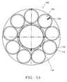
- the embodiment of the baffle assembly 100 shown in FIG. 2Acomprises nine baffle inserts 120 .
- any number of baffle inserts 120may be employed.
- the baffle inserts 120can be disc-shaped. All the baffle inserts 120 can have the same shape, making baffle inserts 120 exchangeable.
- the baffle inserts 120comprises a plurality of passages 122 therethrough in order to permit gas in the process space 12 to be removed by the vacuum pump.
- Various shapes and geometriescan be utilized for the passages 122 as shown in FIGS. 2B, 2C , 2 D, or 2 E.
- each passage 122can have a slot shape and extend radially.
- each passage 122can have a round shape.
- the illustrated passages 122have a higher density near the chuck assembly 30 than away from the chuck assembly 30 .
- each passage 122can have a jagged shape.
- FIG. 2Eillustrates that passages 122 can have letter shapes. In the embodiment “T”, “E”, and “L” shapes are used. Of course, any open polygon shape including letters or characters of any language can be used.
- the baffle carrier 110is formed into a ring surrounding the chuck assembly 30 and can be secured to the chuck assembly 30 with, for example, threaded hardware (not shown).
- the baffle carrier 110comprises holes 112 corresponding to the baffle inserts 120 .
- each hole 112can be formed into a round shape having a diameter smaller than a diameter of the baffle insert 120 .
- Flanges 114can be formed at the rims of the holes 112 .
- the flanges 114can have upper surfaces lower than the upper surface of the baffle carrier 110 , enabling the baffle inserts 120 to rest thereon.
- the baffle inserts 120can be attached to baffle carrier 110 or the baffle inserts 120 can merely lie on baffle carrier 110 .
- FIG. 3Another embodiment of the present invention is illustrated in FIG. 3 .
- a baffle assembly 100has eight baffle inserts 120 but can have at least two baffle inserts.
- the baffle inserts 120can be distributed to adjoin each other and substantially cover the passageway 42 .
- the baffle inserts 120comprise small passages 122 therethrough.
- passages 122are round in the illustrated embodiment, the passages 122 can be placed into any kind of disposition and be formed in any shape, such as, for example, those shapes shown in FIG. 2B, 2C , 2 D, or 2 E.
- the baffle inserts 120can be formed into the same fan shape, enabling them to be exchanged with each other.
- the baffle inserts 120function as exchangeable modular parts.
- the baffle assembly 100comprises a baffle carrier 110 for supporting the baffle inserts 120 .
- the baffle carrier 110defines holes 112 corresponding to the baffle inserts 120 .
- the holes 112have a similar shape as the baffle inserts 120 and can be formed smaller than the baffle inserts 120 so that the periphery of the baffle inserts 120 can be supported by the baffle carrier 110 .
- the baffle inserts 120lie on the baffle carrier 100 and are not secured to any part of the plasma processing system 1 .
- baffle inserts 120can be fastened to baffle carrier 100 .
- the baffle assembly 100comprises baffle inserts 120 substantially screening the passageway 42 , and a baffle carrier 110 for supporting the baffle inserts 120 .
- the baffle inserts 120can be formed into the same fan shape, enabling them to be exchanged with each other. Thus the baffle inserts 120 function as exchangeable modular parts.
- the baffle inserts 120comprise small passages 122 therethrough.
- the baffle inserts 120comprise round shape passages 122 in the illustrated embodiment, the passages 122 can be placed into any kind of disposition and be formed into any shape, such as, for example, those shapes shown in FIG. 2B, 2C , 2 D, or 2 E.
- Baffle carrier 110comprises a baffle carrier ring 116 secured to the chuck assembly 30 .
- the baffle carrier 110consists of a baffle carrier ring 116 surrounding the chuck assembly 30 .
- the baffle carrier ring 116defines a retaining slit 116 B comprising an opening extending downwardly from the top surface of the baffle carrier ring 116 .
- the baffle assembly 100comprises baffle inserts 120 substantially screening the passageway 42 , and a baffle carrier 110 for supporting the baffle inserts 120 .
- the baffle inserts 120are formed into the same shape, enabling them to be exchanged each other.
- the baffle inserts 120function as exchangeable modular parts.
- the baffle inserts 120comprise small passages 122 therethrough.
- the baffle inserts 120comprise round shape passages 122 in the embodiment, the passages 122 can be placed into any kind of disposition and be formed into any kind of shapes, such as, for example, those shapes shown in FIG. 2B, 2C , 2 D, or 2 E.
- the baffle carrier 110can comprise a first baffle carrier ring 116 surrounding the chuck assembly 30 , a second baffle carrier 117 positioned adjacent to the inside of the side wall of the chamber 10 , and support rods 119 located between the first baffle carrier ring 116 and the second baffle carrier ring 117 .
- the first baffle carrier ring 116can be secured to the chuck assembly 30 .
- the second baffle carrier ring 117can be attached to the chamber 10 .
- First ends 119 A of the support rods 119are coupled to the first baffle carrier ring 116 with first mounting hardware 119 B.
- the second baffle ring 117can be secured to the second ends 119 C of the support rods 119 with second mounting hardware 119 D.
- FIG. 6Cillustrates support rods 119 having a U-shape portion on the end thereof.
- the first baffle carrier ring 116comprises tunnel holes 116 C extend horizontally.
- the first ends 119 A of the support rods 119are fitted in the tunnel holes 116 C securely and the support rods are held horizontally or at any other angle.
- the second baffle carrier ring 117comprises tube holes or slots 117 B extending vertically.
- the second end 119 B of the support rods 119are formed in U-shape, and the tip of the second ends 119 B are fitted in the tube holes or slots 117 B.
- a first indent 116 Ais formed on the top surface of the first baffle carrier ring 116 and a second indent 117 A corresponding to the first indent 116 A is formed on the top surface of the second baffle carrier ring 117 .
- the baffle inserts 120can be positioned between the first indent 116 A and the second indent 117 A.
- the baffle inserts 120are installed on the baffle carrier 110 .
- the baffle inserts 120need not be secured to any part of the plasma processing system 1 .
- the removed baffle inserts 120are cleaned. If one or more of the baffle inserts 120 cannot be cleaned, they can be exchanged for new baffle insert(s) 120 . Alternatively, all the removed baffle inserts 120 can be exchanged for new baffle inserts 120 (as shown at 360 ).
Landscapes
- Engineering & Computer Science (AREA)
- Physics & Mathematics (AREA)
- Plasma & Fusion (AREA)
- Chemical & Material Sciences (AREA)
- Analytical Chemistry (AREA)
- General Physics & Mathematics (AREA)
- Condensed Matter Physics & Semiconductors (AREA)
- Manufacturing & Machinery (AREA)
- Computer Hardware Design (AREA)
- Microelectronics & Electronic Packaging (AREA)
- Power Engineering (AREA)
- Chemical Vapour Deposition (AREA)
- Treatment Of Fiber Materials (AREA)
Abstract
Description
- This application is related to U.S. Pat. No. 6,837,966 and U.S. application Ser. No. 10/647,469, filed Aug. 26, 2003, Ser. No. 10/705,224, filed Nov. 12, 2003 and Ser. No. 11/006,544, filed Dec. 8, 2004. The entire contents of each of this patent and these patent applications are herein incorporated by reference in their entirety.
- The present invention relates to a component for a plasma processing system and, more particularly, to a baffle assembly employed in plasma processing system surrounding a substrate holder.
- The fabrication of integrated circuits (IC) in the semiconductor industry typically employs plasma to create and assist surface chemistry within a plasma reactor necessary to remove material from and deposit material to a substrate. In general, plasma is formed within the plasma reactor under vacuum conditions by heating electrons to energies sufficient to sustain ionizing collisions with a supplied process gas. Moreover, the heated electrons can have energy sufficient to sustain dissociative collisions and, therefore, a specific set of gases under predetermined conditions (e.g. chamber pressure, gas flow rate, etc.) are chosen to produce a population of charged species and chemically reactive species suitable to the particular process being performed within the chamber (e.g. etching processes where materials are removed from the substrate or deposition processes where materials are added to the substrate). In general, a vacuum pump provides a reduced pressure atmosphere in a plasma processing chamber. A (pumping) baffle plate comprising a plurality of small passages therethrough is located between the plasma and the pump to confine the plasma while permitting gas to be evacuated. The baffle plate's surface can be exposed to the physically and chemically active plasma, and, in time, can erode. So the baffle plate should be cleaned or replaced periodically.
- The present invention provides a baffle assembly located in a plasma processing system having a chuck assembly for holding a substrate. The baffle assembly includes a baffle carrier attached to the plasma processing system and at least two baffle inserts having a plurality of passages therethrough. The baffle inserts are supported by the baffle carrier.
- These and other aspects of the invention will become more apparent and more readily appreciated from the following detailed description of the exemplary embodiments of the invention taken in conjunction with the accompanying drawings, where:
FIG. 1 shows a simplified block diagram of a plasma processing system comprising a baffle plate according to an embodiment of the present invention;FIG. 2A shows a plan view of a baffle assembly for a plasma processing system according to an embodiment of the present invention;FIGS. 2B-2E show a variety of passages which may be employed in the baffle inserts;FIG. 3 shows a plan view of a baffle assembly for a plasma processing system according to an embodiment of the present invention;FIG. 4A shows a plan view of a baffle assembly for a plasma processing system according to an embodiment of the present invention;FIG. 4B shows a cross sectional view of a baffle assembly for a plasma processing system according to the embodiment ofFIG. 4A ;FIG. 4C shows a cross sectional view of a baffle assembly for a plasma processing system according to an alternative embodiment toFIG. 4B ;FIG. 5A shows a plan view of a baffle assembly for a plasma processing system according to an embodiment of the present invention;FIG. 5B shows a cross sectional view of a baffle assembly for a plasma processing system according to the embodiment ofFIG. 5A ;FIG. 6A shows a plan view of a baffle assembly for a plasma processing system according to an embodiment of the present invention;FIG. 6B shows a cross sectional view of a baffle assembly for a plasma processing system according to the embodiment ofFIG. 6A ;FIG. 6C shows a cross sectional view of a baffle assembly for a plasma processing system according to an alternative embodiment toFIG. 6B ; andFIG. 7 presents a method of maintenance of a plasma processing system according to an embodiment of the present invention.- According to an embodiment of the present invention, a
plasma processing system 1 depicted inFIG. 1 comprises aplasma processing chamber 10, anupper assembly 20 for covering the plasma processing chamber, anupper electrode 22 coupled to theupper assembly 20, asubstrate holder 30 for supporting asubstrate 35, and apumping duct 40 coupled to a vacuum pump (not shown) for providing a reducedpressure atmosphere 11 inplasma processing chamber 10.Plasma processing chamber 10 can facilitate the formation of processing plasma inprocess space 12 adjacent tosubstrate 35. In the plasma processing system apassageway 42 is formed between theprocess space 12 and thepumping duct 40. Theplasma processing system 1 can be configured to process 200 mm substrates, 300 mm substrates, or substrates of any size. - In the illustrated embodiment,
upper electrode 22 comprises anelectrode plate 24 with adeposition shield 26. In an alternate embodiment,upper assembly 20 can comprise a cover, a gas injection assembly, or an upper electrode impedance match network, or any combination of two or more thereof. For example, theupper electrode 22 can be coupled to an RF source. In another alternate embodiment, theupper assembly 20 comprises a cover coupled to theupper electrode 22, wherein theupper electrode 22 is maintained at an electrical potential equivalent to that of theplasma processing chamber 10. For example, theplasma processing chamber 10, theupper assembly 20, and theupper electrode 22 can be electrically connected to ground potential. Plasma processing chamber 10 can further comprise anoptical viewport 16 coupled to thedeposition shield 26 ofupper electrode 22.Optical viewport 16 can permit monitoring of optical emission from the processing plasma inprocess space 12.Chuck assembly 30 forholding substrate 35 can further comprise a verticaltranslational device 50 surrounded by abellows 52 coupled to thechuck assembly 30 and theplasma processing chamber 10, and configured to seal the verticaltranslational device 50 from the reducedpressure atmosphere 11 inplasma processing chamber 10. Additionally, abellows shield 54 can be coupled to thechuck assembly 30 and configured to protect thebellows 52 from the processing plasma.- The
plasma processing system 1 further comprises afocus ring 60, ashield ring 62, and abaffle assembly 100. - Referring now to an illustrated embodiment of the present invention depicted in
FIG. 2A , thebaffle assembly 100 comprises abaffle carrier 110 that can be attached to thechuck assembly 30 or to theprocessing chamber 10 and at least two baffle inserts120. The embodiment of thebaffle assembly 100 shown inFIG. 2A comprises nine baffle inserts120. Of course, any number of baffle inserts120 may be employed. - The baffle inserts120 can be disc-shaped. All the baffle inserts120 can have the same shape, making baffle inserts120 exchangeable.
- The baffle inserts120 comprises a plurality of
passages 122 therethrough in order to permit gas in theprocess space 12 to be removed by the vacuum pump. Various shapes and geometries can be utilized for thepassages 122 as shown inFIGS. 2B, 2C ,2D, or2E. Referring now toFIG. 2B , eachpassage 122 can have a slot shape and extend radially. As shown inFIG. 2C , eachpassage 122 can have a round shape. Although the passages can be formed in any different distribution, the illustratedpassages 122 have a higher density near thechuck assembly 30 than away from thechuck assembly 30. ReferringFIG. 2D , eachpassage 122 can have a jagged shape.FIG. 2E illustrates thatpassages 122 can have letter shapes. In the embodiment “T”, “E”, and “L” shapes are used. Of course, any open polygon shape including letters or characters of any language can be used. - The
baffle carrier 110, as depictedFIG. 2A , is formed into a ring surrounding thechuck assembly 30 and can be secured to thechuck assembly 30 with, for example, threaded hardware (not shown). Thebaffle carrier 110 comprisesholes 112 corresponding to the baffle inserts120. In the embodiment eachhole 112 can be formed into a round shape having a diameter smaller than a diameter of thebaffle insert 120. Thus theholes 112 do not permit thebaffle insert 120 to pass therethrough.Flanges 114 can be formed at the rims of theholes 112. Theflanges 114 can have upper surfaces lower than the upper surface of thebaffle carrier 110, enabling the baffle inserts120 to rest thereon. The baffle inserts120 can be attached to bafflecarrier 110 or the baffle inserts120 can merely lie onbaffle carrier 110. - Another embodiment of the present invention is illustrated in
FIG. 3 . In the embodiment abaffle assembly 100 has eight baffle inserts120 but can have at least two baffle inserts. The baffle inserts120 can be distributed to adjoin each other and substantially cover thepassageway 42. The baffle inserts120 comprisesmall passages 122 therethrough. Althoughpassages 122 are round in the illustrated embodiment, thepassages 122 can be placed into any kind of disposition and be formed in any shape, such as, for example, those shapes shown inFIG. 2B, 2C ,2D, or2E. The baffle inserts120 can be formed into the same fan shape, enabling them to be exchanged with each other. Thus the baffle inserts120 function as exchangeable modular parts. - The
baffle assembly 100 comprises abaffle carrier 110 for supporting the baffle inserts120. Thebaffle carrier 110 definesholes 112 corresponding to the baffle inserts120. Theholes 112 have a similar shape as the baffle inserts120 and can be formed smaller than the baffle inserts120 so that the periphery of the baffle inserts120 can be supported by thebaffle carrier 110. In this embodiment the baffle inserts120 lie on thebaffle carrier 100 and are not secured to any part of theplasma processing system 1. Alternatively, baffle inserts120 can be fastened to bafflecarrier 100. - Another embodiment of the present invention is illustrated in
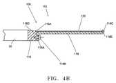
FIGS. 4A and 4B . Thebaffle assembly 100 comprises abaffle carrier 110 and baffle inserts120. Thebaffle carrier 110 comprisesbaffle carrier ring 116 surrounding thechuck assembly 30, and baffle carrier supports118 mounted to thebaffle carrier ring 116. In the illustrated embodiment thebaffle carrier 110 has eight baffle carrier supports118, but any number of baffle carrier supports can be chosen for supporting a corresponding number of baffle inserts120. The baffle inserts120 comprisesmall passages 122 therethrough. Although the baffle inserts120 compriseround shape passages 122 in the illustrated embodiment, thepassages 122 can be placed into any kind of disposition and be formed in any shape, such as, for example, those shapes shown inFIG. 2B, 2C ,2D, or2E. - As shown
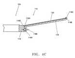
FIG. 4B , the baffle carrier supports118 can be secured to thebaffle carrier ring 116 attached to thechuck assembly 30. Specifically, the baffle carrier supports comprisetabs 118A on the first ends118D and thetabs 118A can be attached to thebaffle carrier ring 116 with mountinghardware 118B. The baffle carrier supports118 havesmall projections 118C above the second ends118E thereof so that the baffle inserts120 can be positioned on the baffle carrier supports118. Further, asmall indent 116A can be formed on the top of thebaffle carrier ring 116 to position the baffle inserts between theprojections 118C and theindent 116A. The baffle carrier supports118 can be placed substantially horizontally. Thus the baffle inserts120 can be kept substantially horizontal. On the other hand, the baffle carrier supports118 are placed can be positioned at angles other than horizontal. For example, as shown inFIG. 4C , the baffle carrier supports118 can be inclined relative to horizontal. Specifically, the second ends118E of the baffle carrier supports118 depicted inFIG. 4C are positioned higher than the first ends118D. Thus the baffle inserts120 are positioned at an incline. - Another embodiment of the present invention is illustrated in
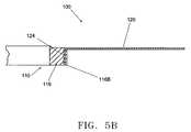
FIGS. 5A and 5B . In this embodiment, thebaffle assembly 100 comprises baffle inserts120 substantially screening thepassageway 42, and abaffle carrier 110 for supporting the baffle inserts120. The baffle inserts120 can be formed into the same fan shape, enabling them to be exchanged with each other. Thus the baffle inserts120 function as exchangeable modular parts. The baffle inserts120 comprisesmall passages 122 therethrough. Although the baffle inserts120 compriseround shape passages 122 in the illustrated embodiment, thepassages 122 can be placed into any kind of disposition and be formed into any shape, such as, for example, those shapes shown inFIG. 2B, 2C ,2D, or2E. Baffle carrier 110 comprises abaffle carrier ring 116 secured to thechuck assembly 30. In the embodiment shown inFIG. 5B thebaffle carrier 110 consists of abaffle carrier ring 116 surrounding thechuck assembly 30. Thebaffle carrier ring 116 defines a retainingslit 116B comprising an opening extending downwardly from the top surface of thebaffle carrier ring 116.- The baffle inserts120 have
baffle tabs 124 which can be inserted into the retaining slit116B to support the baffle inserts120. The shape ofbaffle tabs 124 can be formed to be readily inserted into the retaining slit116B and be readily removed from the retaining slit116B. - Another embodiment of the present invention is illustrated in
FIGS. 6A and 6B . In this embodiment thebaffle assembly 100 comprises baffle inserts120 substantially screening thepassageway 42, and abaffle carrier 110 for supporting the baffle inserts120. The baffle inserts120 are formed into the same shape, enabling them to be exchanged each other. Thus the baffle inserts120 function as exchangeable modular parts. The baffle inserts120 comprisesmall passages 122 therethrough. Although the baffle inserts120 compriseround shape passages 122 in the embodiment, thepassages 122 can be placed into any kind of disposition and be formed into any kind of shapes, such as, for example, those shapes shown inFIG. 2B, 2C ,2D, or2E. - The
baffle carrier 110 can comprise a firstbaffle carrier ring 116 surrounding thechuck assembly 30, asecond baffle carrier 117 positioned adjacent to the inside of the side wall of thechamber 10, andsupport rods 119 located between the firstbaffle carrier ring 116 and the secondbaffle carrier ring 117. The firstbaffle carrier ring 116 can be secured to thechuck assembly 30. Alternatively, or in addition, the secondbaffle carrier ring 117 can be attached to thechamber 10. First ends119A of thesupport rods 119 are coupled to the firstbaffle carrier ring 116 with first mountinghardware 119B. Thesecond baffle ring 117 can be secured to the second ends119C of thesupport rods 119 with second mountinghardware 119D. The firstbaffle carrier ring 116 and the secondbaffle carrier ring 117 can be at substantially the same height so that the baffle inserts120 can be horizontally supported by the firstbaffle carrier ring 116 and the secondbaffle carrier ring 117. Alternatively, the secondbaffle carrier ring 117 can be at a different height than firstbaffle carrier ring 116 so that baffle inserts120 are at an angle. Afirst indent 116A is formed on the top surface of the firstbaffle carrier ring 116 and asecond indent 117A corresponding to thefirst indent 116A is formed on the top surface of the secondbaffle carrier ring 117. The baffle inserts120 can be positioned between thefirst indent 116A and thesecond indent 117A. - The baffle inserts120 can be supported by any different structure.
FIG. 6C illustratessupport rods 119 having a U-shape portion on the end thereof. The firstbaffle carrier ring 116 comprises tunnel holes116C extend horizontally. The first ends119A of thesupport rods 119 are fitted in the tunnel holes116C securely and the support rods are held horizontally or at any other angle. The secondbaffle carrier ring 117 comprises tube holes orslots 117B extending vertically. Thesecond end 119B of thesupport rods 119 are formed in U-shape, and the tip of the second ends119B are fitted in the tube holes orslots 117B. Afirst indent 116A is formed on the top surface of the firstbaffle carrier ring 116 and asecond indent 117A corresponding to thefirst indent 116A is formed on the top surface of the secondbaffle carrier ring 117. The baffle inserts120 can be positioned between thefirst indent 116A and thesecond indent 117A. FIG. 7 presents the method of maintenance of a plasma processing system described inFIGS. 1-6C according to an embodiment of the present invention. Flow diagram200 begins at210 in which thebaffle carrier 110 is attached to theplasma processing system 1. For example, thebaffle carrier 110 can be attached to thechuck assembly 30 in theplasma processing system 1.- At220, the baffle inserts120 are installed on the
baffle carrier 110. The baffle inserts120 need not be secured to any part of theplasma processing system 1. - After the
baffle assembly 100 comprising thebaffle carrier 110 and baffle inserts120 are installed to theplasma processing system 1, theplasma processing system 1 is operated at230. After some period of use, the baffle assembly should be replaced or cleaned periodically. - At240, when maintenance of the
plasma processing system 1 is required, theplasma processing system 1 is deactivated. At250, the baffle inserts120 are removed from theplasma processing system 1. Since the baffle inserts120 can merely lie on thebaffle carrier 110, maintenance personnel do not need to disassemble other parts in theplasma processing system 1 and can easily remove the baffle inserts120 from theplasma processing system 1. - At260, the removed baffle inserts120 are cleaned. If one or more of the baffle inserts120 cannot be cleaned, they can be exchanged for new baffle insert(s)120. Alternatively, all the removed baffle inserts120 can be exchanged for new baffle inserts120 (as shown at360).
- At270, the cleaned baffle inserts120 are replaced in the
plasma processing system 1. Specifically, the cleaned baffle inserts120 can be installed on thebaffle carrier 110. In the case where one or more of the baffle inserts are exchanged to new baffle insert(s), the new baffle insert(s) are installed to theplasma processing system 1. Further, all of the baffle inserts are exchanged with other baffle insert(s), the other baffle insert(s) are installed to the plasma processing system1 (as shown at370). At270 and370, maintenance personnel may not need to secure the baffle inserts to any part of theplasma processing system 1. - Although only certain exemplary embodiments of this invention have been described in detail above, those skilled in the art will readily appreciate that many modifications are possible in the exemplary embodiments without materially departing from the novel teachings and advantages of this invention. Accordingly, all such modifications are intended to be included within the scope of this invention.
Claims (27)
1. A baffle assembly located in a plasma processing system having a chuck assembly for holding a substrate, comprising:
a baffle carrier attached to the plasma processing system; and
at least two baffle inserts having a plurality of passages therethrough, the at least two baffle inserts being supported by the baffle carrier.
2. The baffle assembly as recited inclaim 1 , wherein the at least two baffle inserts are not secured to any part of the plasma processing system.
3. The baffle assembly as recited inclaim 1 , wherein the at least two baffle inserts have the same shape.
4. The baffle assembly as recited inclaim 1 , wherein each of the at least two baffle inserts are adjacent to each other.
5. The baffle assembly as recited inclaim 1 , wherein the at least two baffle inserts have a disk shape.
6. The baffle assembly as recited inclaim 1 , wherein the plasma processing system includes a passageway for gas, and the at least two baffle inserts cover substantially the entire passageway.
7. The baffle assembly as recited inclaim 1 , wherein the baffle carrier comprises a baffle carrier ring attached to the chuck assembly and baffle carrier supports secured to the baffle carrier ring, and edges of the at least two baffle inserts are supported by the baffle carrier supports.
8. The baffle assembly as recited inclaim 1 , wherein the baffle carrier comprises a baffle carrier ring attached to the plasma processing system and having a slot, and each of the at least two baffle inserts further comprises a tab inserted into the slot.
9. The baffle assembly as recited inclaim 1 , wherein the baffle carrier comprises a first baffle carrier ring attached to the plasma processing system, support rods having first ends secured to the baffle carrier ring, and a second baffle carrier ring secured to the second ends of said support rods, the at least two baffle inserts resting on at least the baffle carrier ring and the second baffle carrier ring.
10. The baffle assembly as recited inclaim 1 , wherein the baffle inserts are substantially horizontal.
11. The baffle assembly as recited inclaim 1 , wherein the baffle inserts are inclined relative to horizontal.
12. A plasma processing system comprising:
a processing chamber;
a chuck assembly disposed in said chamber for holding a substrate; and
a baffle assembly located in the processing chamber, wherein said baffle assembly comprises a baffle carrier attached to the plasma processing system, and at least two baffle inserts having a plurality of passages therethrough, the at least two baffle inserts being supported by the baffle carrier.
13. The plasma processing system as recited inclaim 12 , wherein the at least two baffle inserts are not secured to any part of the plasma processing system.
14. The plasma processing system as recited inclaim 12 , wherein the at least two baffle inserts have the same shape.
15. The plasma processing system as recited inclaim 12 , wherein each of the at least two baffle inserts are adjacent to each other.
16. The plasma processing system as recited inclaim 12 , wherein the at least two baffle inserts have a disk shape.
17. The plasma processing system as recited inclaim 12 , wherein the plasma processing system includes a passageway for gas, and the at least two baffle inserts cover substantially the entire passageway.
18. The plasma processing system as recited inclaim 12 , wherein the baffle carrier comprises a baffle carrier ring attached to the chuck assembly and baffle carrier supports secured to the baffle carrier ring, and edges of the at least two baffle inserts are supported by the baffle carrier supports.
19. The plasma processing system as recited inclaim 12 , wherein the baffle carrier comprises a baffle carrier ring attached to the plasma processing system and having a slot, and the each of at least two baffle inserts further comprises a tab inserted into the slot.
20. The plasma processing system as recited inclaim 12 , wherein the baffle carrier comprises a first baffle carrier ring attached to the plasma processing system, support rods having first ends secured to the baffle carrier ring, and a second baffle carrier ring secured to the second ends of said support rods, the at least two baffle inserts resting on at least the baffle carrier ring and the second baffle carrier ring.
21. The plasma processing system as recited inclaim 12 , wherein the baffle inserts are substantially horizontal.
22. The plasma processing system as recited inclaim 12 , wherein the baffle inserts are inclined relative to horizontal.
23. The plasma processing system as recited inclaim 12 , wherein the baffle carrier is coupled to the chuck assembly.
24. A method of maintaining a plasma processing system having a chuck assembly for holding a substrate, said method comprising:
deactivating said plasma processing system having a baffle assembly therein, the baffle assembly comprises a baffle carrier attached to said plasma processing system, and at least two baffle inserts having a plurality of passages therethrough and being supported by the baffle carrier;
removing said at least two baffle inserts from the plasma processing system without removing the baffle carrier;
cleaning the at least two baffle inserts; and
replacing the cleaned at least two baffle inserts on the baffle carrier.
25. A method of maintaining a plasma processing system as recited inclaim 24 , wherein the at least two baffle inserts are not secured to any part of the plasma processing system.
26. A method of maintaining a plasma processing system having a chuck assembly for holding a substrate, said method comprising:
deactivating a plasma processing system having a baffle assembly therein, the baffle assembly comprises a baffle carrier attached to said plasma processing system, and at least two baffle inserts having a plurality of passages therethrough and being supported by the baffle carrier;
removing said at least two baffle inserts from the plasma processing system without removing the baffle carrier; and
placing at least two other baffle inserts onto the baffle carrier instead of replacing the removed at least two baffle inserts.
27. A method of maintenance of a plasma processing system as recited inclaim 26 , wherein the at least two baffle inserts are not secured to any part of the plasma processing system.
Priority Applications (3)
| Application Number | Priority Date | Filing Date | Title |
|---|---|---|---|
| US11/032,101US7601242B2 (en) | 2005-01-11 | 2005-01-11 | Plasma processing system and baffle assembly for use in plasma processing system |
| PCT/US2006/000591WO2006076253A2 (en) | 2005-01-11 | 2006-01-10 | Plasma processing system and baffle assembly for use in plasma processing system |
| TW095101019ATW200710984A (en) | 2005-01-11 | 2006-05-23 | Plasma processing system and baffle assembly for use in plasma processing system |
Applications Claiming Priority (1)
| Application Number | Priority Date | Filing Date | Title |
|---|---|---|---|
| US11/032,101US7601242B2 (en) | 2005-01-11 | 2005-01-11 | Plasma processing system and baffle assembly for use in plasma processing system |
Publications (2)
| Publication Number | Publication Date |
|---|---|
| US20060151114A1true US20060151114A1 (en) | 2006-07-13 |
| US7601242B2 US7601242B2 (en) | 2009-10-13 |
Family
ID=36652078
Family Applications (1)
| Application Number | Title | Priority Date | Filing Date |
|---|---|---|---|
| US11/032,101Expired - Fee RelatedUS7601242B2 (en) | 2005-01-11 | 2005-01-11 | Plasma processing system and baffle assembly for use in plasma processing system |
Country Status (3)
| Country | Link |
|---|---|
| US (1) | US7601242B2 (en) |
| TW (1) | TW200710984A (en) |
| WO (1) | WO2006076253A2 (en) |
Cited By (23)
| Publication number | Priority date | Publication date | Assignee | Title |
|---|---|---|---|---|
| US20050103267A1 (en)* | 2003-11-14 | 2005-05-19 | Hur Gwang H. | Flat panel display manufacturing apparatus |
| US20050217580A1 (en)* | 2003-05-30 | 2005-10-06 | Aviza Technology, Inc. | Gas distribution system |
| US20050224179A1 (en)* | 2002-05-22 | 2005-10-13 | Tokyo Electron Korea Ltd. | Baffle plate and plasma etching device having same |
| US20070022959A1 (en)* | 2005-07-29 | 2007-02-01 | Craig Bercaw | Deposition apparatus for semiconductor processing |
| US7552521B2 (en)* | 2004-12-08 | 2009-06-30 | Tokyo Electron Limited | Method and apparatus for improved baffle plate |
| US20090206055A1 (en)* | 2008-02-20 | 2009-08-20 | Tokyo Electron Limited | Plasma processing apparatus and method, and baffle plate of the plasma processing apparatus |
| US7601242B2 (en) | 2005-01-11 | 2009-10-13 | Tokyo Electron Limited | Plasma processing system and baffle assembly for use in plasma processing system |
| US20110024040A1 (en)* | 2009-07-28 | 2011-02-03 | Tokyo Electron Limited | Deposit protection cover and plasma processing apparatus |
| US20110284166A1 (en)* | 2008-04-07 | 2011-11-24 | Carducci James D | Lower liner with integrated flow equalizer and improved conductance |
| US20110287632A1 (en)* | 2010-05-21 | 2011-11-24 | Lam Research Corporation | Movable chamber liner plasma confinement screen combination for plasma processing apparatuses |
| US20130284288A1 (en)* | 2012-04-30 | 2013-10-31 | Semes Co., Ltd. | Adjustment plate and apparatus for treating substrate having the same |
| US20140087093A1 (en)* | 2011-04-07 | 2014-03-27 | Picosun Oy | Deposition reactor with plasma source |
| US20140261176A1 (en)* | 2013-03-15 | 2014-09-18 | Taiwan Semiconductor Manufacturing Company Limited | Pumping liner for chemical vapor deposition |
| WO2017180856A1 (en)* | 2016-04-15 | 2017-10-19 | Applied Materials, Inc. | Micro-volume deposition chamber |
| US20190119815A1 (en)* | 2017-10-24 | 2019-04-25 | Applied Materials, Inc. | Systems and processes for plasma filtering |
| US20200243305A1 (en)* | 2019-01-25 | 2020-07-30 | Mattson Technology, Inc. | Post Plasma Gas Injection In A Separation Grid |
| US10950419B2 (en)* | 2017-08-22 | 2021-03-16 | Samsung Electronics Co., Ltd. | Shrouds and substrate treating systems including the same |
| US20210130955A1 (en)* | 2018-07-27 | 2021-05-06 | Tokyo Electron Limited | Film forming apparatus and film forming method |
| US20210398781A1 (en)* | 2018-11-12 | 2021-12-23 | Jiangsu Leuven Instruments Co. Ltd | Reaction chamber lining |
| US20220051912A1 (en)* | 2020-08-12 | 2022-02-17 | Taiwan Semiconductor Manufacturing Company Limited | Gas flow control during semiconductor fabrication |
| US11685994B2 (en)* | 2019-09-13 | 2023-06-27 | Taiwan Semiconductor Manufacturing Co., Ltd. | CVD device pumping liner |
| US20240014015A1 (en)* | 2021-02-12 | 2024-01-11 | Lam Research Corporation | C-shroud Modification For Plasma Uniformity Without Impacting Mechanical Strength Or Lifetime Of The C-shroud |
| US20250062139A1 (en)* | 2023-08-17 | 2025-02-20 | Taiwan Semiconductor Manufacturing Company, Ltd. | Furnace inner tube for process uniformity |
Families Citing this family (7)
| Publication number | Priority date | Publication date | Assignee | Title |
|---|---|---|---|---|
| US6844260B2 (en)* | 2003-01-30 | 2005-01-18 | Micron Technology, Inc. | Insitu post atomic layer deposition destruction of active species |
| JP5102706B2 (en)* | 2008-06-23 | 2012-12-19 | 東京エレクトロン株式会社 | Baffle plate and substrate processing apparatus |
| US9129778B2 (en) | 2011-03-18 | 2015-09-08 | Lam Research Corporation | Fluid distribution members and/or assemblies |
| KR101814013B1 (en)* | 2011-05-09 | 2018-01-03 | 삼성디스플레이 주식회사 | Plasma device |
| US10316409B2 (en)* | 2012-12-21 | 2019-06-11 | Novellus Systems, Inc. | Radical source design for remote plasma atomic layer deposition |
| US10604841B2 (en) | 2016-12-14 | 2020-03-31 | Lam Research Corporation | Integrated showerhead with thermal control for delivering radical and precursor gas to a downstream chamber to enable remote plasma film deposition |
| WO2019113478A1 (en) | 2017-12-08 | 2019-06-13 | Lam Research Corporation | Integrated showerhead with improved hole pattern for delivering radical and precursor gas to a downstream chamber to enable remote plasma film deposition |
Citations (89)
| Publication number | Priority date | Publication date | Assignee | Title |
|---|---|---|---|---|
| US4263088A (en)* | 1979-06-25 | 1981-04-21 | Motorola, Inc. | Method for process control of a plasma reaction |
| US4310390A (en)* | 1977-08-10 | 1982-01-12 | Lockheed Corporation | Protective coating process for aluminum and aluminum alloys |
| US4367114A (en)* | 1981-05-06 | 1983-01-04 | The Perkin-Elmer Corporation | High speed plasma etching system |
| US4579618A (en)* | 1984-01-06 | 1986-04-01 | Tegal Corporation | Plasma reactor apparatus |
| US4590042A (en)* | 1984-12-24 | 1986-05-20 | Tegal Corporation | Plasma reactor having slotted manifold |
| US4649858A (en)* | 1984-10-12 | 1987-03-17 | Sumitomo Metal Industries, Ltd. | Repairing apparatus for furnace wall |
| US4820371A (en)* | 1987-12-15 | 1989-04-11 | Texas Instruments Incorporated | Apertured ring for exhausting plasma reactor gases |
| US4985102A (en)* | 1986-07-17 | 1991-01-15 | Du Pont Canada Inc. | Method of making fiber reinforced polyamide sheets |
| US5000113A (en)* | 1986-12-19 | 1991-03-19 | Applied Materials, Inc. | Thermal CVD/PECVD reactor and use for thermal chemical vapor deposition of silicon dioxide and in-situ multi-step planarized process |
| US5006220A (en)* | 1987-10-26 | 1991-04-09 | Tokyo Ohka Kogyo Co., Ltd. | Electrode for use in the treatment of an object in a plasma |
| US5180467A (en)* | 1990-08-08 | 1993-01-19 | Vlsi Technology, Inc. | Etching system having simplified diffuser element removal |
| US5411568A (en)* | 1994-05-25 | 1995-05-02 | Harmony Products Inc. | Highly available waste based nitrogen fertilizer |
| US5484752A (en)* | 1993-11-12 | 1996-01-16 | Ube Industries, Ltd. | Ceramic composite material |
| US5489449A (en)* | 1990-03-28 | 1996-02-06 | Nisshin Flour Milling Co., Ltd. | Coated particles of inorganic or metallic materials and processes of producing the same |
| US5494713A (en)* | 1994-02-03 | 1996-02-27 | Tokyo Electron Limited | Method for treating surface of aluminum material and plasma treating apparatus |
| US5521790A (en)* | 1994-05-12 | 1996-05-28 | International Business Machines Corporation | Electrostatic chuck having relatively thick and thin areas and means for uniformly cooling said thick and thin areas during chuck anodization |
| US5593540A (en)* | 1992-10-19 | 1997-01-14 | Hitachi, Ltd. | Plasma etching system and plasma etching method |
| US5595627A (en)* | 1995-02-07 | 1997-01-21 | Tokyo Electron Limited | Plasma etching method |
| US5614055A (en)* | 1993-08-27 | 1997-03-25 | Applied Materials, Inc. | High density plasma CVD and etching reactor |
| US5716485A (en)* | 1995-06-07 | 1998-02-10 | Varian Associates, Inc. | Electrode designs for controlling uniformity profiles in plasma processing reactors |
| US5725960A (en)* | 1992-12-28 | 1998-03-10 | Nippon Zeon Co., Ltd. | Molded articles having hard coat layer and method for producing same |
| US5746875A (en)* | 1994-09-16 | 1998-05-05 | Applied Materials, Inc. | Gas injection slit nozzle for a plasma process reactor |
| US5856240A (en)* | 1993-04-05 | 1999-01-05 | Applied Materials, Inc. | Chemical vapor deposition of a thin film onto a substrate |
| US5868848A (en)* | 1995-06-07 | 1999-02-09 | Tokyo Electron Limited | Plasma processing apparatus |
| US5879575A (en)* | 1995-11-29 | 1999-03-09 | Applied Materials, Inc. | Self-cleaning plasma processing reactor |
| US5882411A (en)* | 1996-10-21 | 1999-03-16 | Applied Materials, Inc. | Faceplate thermal choke in a CVD plasma reactor |
| US5885356A (en)* | 1994-11-30 | 1999-03-23 | Applied Materials, Inc. | Method of reducing residue accumulation in CVD chamber using ceramic lining |
| US5885402A (en)* | 1996-07-17 | 1999-03-23 | Applied Materials | Diagnostic head assembly for plasma chamber |
| US5888907A (en)* | 1996-04-26 | 1999-03-30 | Tokyo Electron Limited | Plasma processing method |
| US5892278A (en)* | 1996-05-24 | 1999-04-06 | Dai Nippon Printingco., Ltd. | Aluminum and aluminum alloy radiator for semiconductor device and process for producing the same |
| US5891253A (en)* | 1993-05-14 | 1999-04-06 | Applied Materials, Inc. | Corrosion resistant apparatus |
| US5891350A (en)* | 1994-12-15 | 1999-04-06 | Applied Materials, Inc. | Adjusting DC bias voltage in plasma chambers |
| US5895586A (en)* | 1994-05-17 | 1999-04-20 | Hitachi, Ltd. | Plasma processing apparatus and plasma processing method in which a part of the processing chamber is formed using a pre-fluorinated material of aluminum |
| US5894887A (en)* | 1995-11-30 | 1999-04-20 | Applied Materials, Inc. | Ceramic dome temperature control using heat pipe structure and method |
| US5900103A (en)* | 1994-04-20 | 1999-05-04 | Tokyo Electron Limited | Plasma treatment method and apparatus |
| US5900064A (en)* | 1997-05-01 | 1999-05-04 | Applied Materials, Inc. | Plasma process chamber |
| US5902763A (en)* | 1995-01-19 | 1999-05-11 | Ube Industries, Inc. | Fused ceramic composite |
| US5904778A (en)* | 1996-07-26 | 1999-05-18 | Applied Materials, Inc. | Silicon carbide composite article particularly useful for plasma reactors |
| US6063441A (en)* | 1997-12-02 | 2000-05-16 | Applied Materials, Inc. | Processing chamber and method for confining plasma |
| US6068729A (en)* | 1997-03-03 | 2000-05-30 | Applied Materials, Inc. | Two step process for cleaning a substrate processing chamber |
| US6170429B1 (en)* | 1998-09-30 | 2001-01-09 | Lam Research Corporation | Chamber liner for semiconductor process chambers |
| US6176969B1 (en)* | 1998-04-22 | 2001-01-23 | Samsung Electronics Co., Ltd. | Baffle plate of dry etching apparatus for manufacturing semiconductor devices |
| US6182603B1 (en)* | 1998-07-13 | 2001-02-06 | Applied Komatsu Technology, Inc. | Surface-treated shower head for use in a substrate processing chamber |
| US6210486B1 (en)* | 1997-07-16 | 2001-04-03 | Tokyo Electron Limited | CVD film forming method in which a film formation preventing gas is supplied in a direction from a rear surface of an object to be processed |
| US20010000104A1 (en)* | 1998-12-28 | 2001-04-05 | Lumin Li | Perforated plasma confinement ring in plasma reactors |
| US6221202B1 (en)* | 1999-04-01 | 2001-04-24 | International Business Machines Corporation | Efficient plasma containment structure |
| US6335293B1 (en)* | 1998-07-13 | 2002-01-01 | Mattson Technology, Inc. | Systems and methods for two-sided etch of a semiconductor substrate |
| US20020011215A1 (en)* | 1997-12-12 | 2002-01-31 | Goushu Tei | Plasma treatment apparatus and method of manufacturing optical parts using the same |
| US20020018902A1 (en)* | 2000-06-29 | 2002-02-14 | Toshihiko Tsukatani | Method for thermal spray coating and rare earth oxide powder used therefor |
| US6364949B1 (en)* | 1999-10-19 | 2002-04-02 | Applied Materials, Inc. | 300 mm CVD chamber design for metal-organic thin film deposition |
| US6368987B1 (en)* | 1997-09-30 | 2002-04-09 | Tokyo Electron Limited | Apparatus and method for preventing the premature mixture of reactant gases in CVD and PECVD reactions |
| US6373573B1 (en)* | 2000-03-13 | 2002-04-16 | Lj Laboratories L.L.C. | Apparatus for measuring optical characteristics of a substrate and pigments applied thereto |
| US6383964B1 (en)* | 1998-11-27 | 2002-05-07 | Kyocera Corporation | Ceramic member resistant to halogen-plasma corrosion |
| US6383333B1 (en)* | 1998-04-28 | 2002-05-07 | Tokai Carbon Company, Ltd. | Protective member for inner surface of chamber and plasma processing apparatus |
| US6387817B1 (en)* | 1999-09-07 | 2002-05-14 | Agere Systems Guardian Corp. | Plasma confinement shield |
| US20030000648A1 (en)* | 1998-09-23 | 2003-01-02 | Samsung Electronics Co., Ltd. | Process chamber used in manufacture of semiconductor device, capable of reducing contamination by particulates |
| US20030010446A1 (en)* | 1999-04-16 | 2003-01-16 | Morio Kajiyama | Method of manufacturing a processing apparatus |
| US20030019579A1 (en)* | 2001-07-24 | 2003-01-30 | Samsung Electronics Co., Ltd. | Dry etching apparatus for manufacturing semiconductor devices |
| US6514377B1 (en)* | 1999-09-08 | 2003-02-04 | Tokyo Electron Limited | Apparatus for and method of processing an object to be processed |
| US6519037B2 (en)* | 1999-12-23 | 2003-02-11 | Lj Laboratories, Llc | Spectrometer having optical unit including a randomized fiber optic implement |
| US20030029563A1 (en)* | 2001-08-10 | 2003-02-13 | Applied Materials, Inc. | Corrosion resistant coating for semiconductor processing chamber |
| US6527911B1 (en)* | 2001-06-29 | 2003-03-04 | Lam Research Corporation | Configurable plasma volume etch chamber |
| US6533910B2 (en)* | 2000-12-29 | 2003-03-18 | Lam Research Corporation | Carbonitride coated component of semiconductor processing equipment and method of manufacturing thereof |
| US6537419B1 (en)* | 2000-04-26 | 2003-03-25 | David W. Kinnard | Gas distribution plate assembly for providing laminar gas flow across the surface of a substrate |
| US6537429B2 (en)* | 2000-12-29 | 2003-03-25 | Lam Research Corporation | Diamond coatings on reactor wall and method of manufacturing thereof |
| US6554906B1 (en)* | 2000-01-20 | 2003-04-29 | Sumitomo Electric Industries, Ltd. | Wafer holder for semiconductor manufacturing apparatus and semiconductor manufacturing apparatus using the same |
| US6673198B1 (en)* | 1999-12-22 | 2004-01-06 | Lam Research Corporation | Semiconductor processing equipment having improved process drift control |
| US6676803B2 (en)* | 2001-06-14 | 2004-01-13 | Samsung Electronics Co., Ltd. | Semiconductor device fabricating equipment using radio frequency energy |
| US6695929B2 (en)* | 2001-02-07 | 2004-02-24 | Sumitomo Special Co., Ltd. | Method of making material alloy for iron-based rare earth magnet |
| US20040035364A1 (en)* | 2000-11-13 | 2004-02-26 | Riki Tomoyoshi | Plasma processing apparatus and method for asssembling the plasma processing apparatus |
| US20040050495A1 (en)* | 2002-09-13 | 2004-03-18 | Masahiro Sumiya | Plasma processing apparatus and plasma processing method |
| US20040063333A1 (en)* | 2002-09-30 | 2004-04-01 | Tokyo Electron Limited | Method and apparatus for an improved baffle plate in a plasma processing system |
| US20040060516A1 (en)* | 2002-09-30 | 2004-04-01 | Tokyo Electron Limited | Method and apparatus for an improved optical window deposition shield in a plasma processing system |
| US20040060656A1 (en)* | 2002-09-30 | 2004-04-01 | Tokyo Electron Limited | Method and apparatus for an improved bellows shield in a plasma processing system |
| US20040060661A1 (en)* | 2002-09-30 | 2004-04-01 | Tokyo Electron Limited | Method and apparatus for an improved upper electrode plate with deposition shield in a plasma processing system |
| US20040060658A1 (en)* | 2002-09-30 | 2004-04-01 | Tokyo Electron Limited | Method and apparatus for an improved baffle plate in a plasma processing system |
| US20040060657A1 (en)* | 2002-09-30 | 2004-04-01 | Tokyo Electron Limited | Method and apparatus for an improved deposition shield in a plasma processing system |
| US20040061447A1 (en)* | 2002-09-30 | 2004-04-01 | Tokyo Electron Limited | Method and apparatus for an improved upper electrode plate in a plasma processing system |
| US20040060779A1 (en)* | 2002-10-01 | 2004-04-01 | Charles Kreger | Distance compensating shim for clutch/brake and method of determining same |
| US20040072426A1 (en)* | 2002-08-02 | 2004-04-15 | Soon-Jong Jung | Process chamber for manufacturing a smiconductor device |
| US20040074605A1 (en)* | 2001-02-15 | 2004-04-22 | Takaaki Nezu | Focus ring for semiconductor treatment and plasma treatment device |
| US20040081746A1 (en)* | 2000-12-12 | 2004-04-29 | Kosuke Imafuku | Method for regenerating container for plasma treatment, member inside container for plasma treatment, method for preparing member inside container for plasma treatment, and apparatus for plasma treatment |
| US20050011447A1 (en)* | 2003-07-14 | 2005-01-20 | Tokyo Electron Limited | Method and apparatus for delivering process gas to a process chamber |
| US6852433B2 (en)* | 2002-07-19 | 2005-02-08 | Shin-Etsu Chemical Co., Ltd. | Rare-earth oxide thermal spray coated articles and powders for thermal spraying |
| US20050041238A1 (en)* | 2003-08-19 | 2005-02-24 | Tokyo Electron Limited | Method of using a sensor gas to determine erosion level of consumable system components |
| US6863594B2 (en)* | 2000-03-15 | 2005-03-08 | Paul-Eric Preising | Method and device for cleaning high-voltage carrying installation component parts |
| US6875477B2 (en)* | 2003-02-04 | 2005-04-05 | Hitachi High-Technologies Corporation | Method for coating internal surface of plasma processing chamber |
| US6884516B2 (en)* | 1999-12-10 | 2005-04-26 | Tocalo Co., Ltd. | Internal member for plasma-treating vessel and method of producing the same |
| US7001482B2 (en)* | 2003-11-12 | 2006-02-21 | Tokyo Electron Limited | Method and apparatus for improved focus ring |
Family Cites Families (185)
| Publication number | Priority date | Publication date | Assignee | Title |
|---|---|---|---|---|
| US4209357A (en) | 1979-05-18 | 1980-06-24 | Tegal Corporation | Plasma reactor apparatus |
| JPS5623745A (en) | 1979-08-01 | 1981-03-06 | Hitachi Ltd | Plasma etching device |
| US4270999A (en) | 1979-09-28 | 1981-06-02 | International Business Machines Corporation | Method and apparatus for gas feed control in a dry etching process |
| US4297162A (en) | 1979-10-17 | 1981-10-27 | Texas Instruments Incorporated | Plasma etching using improved electrode |
| JPS63450Y2 (en) | 1980-03-26 | 1988-01-07 | ||
| US4357387A (en) | 1981-08-20 | 1982-11-02 | Subtex, Inc. | Flame resistant insulating fabric compositions prepared by plasma spraying |
| JPS5857491A (en) | 1981-09-30 | 1983-04-05 | Sony Corp | Preparation of green fluorescent material |
| JPS59159510A (en) | 1983-03-01 | 1984-09-10 | Canon Inc | magneto-optical recording medium |
| JPS59186325U (en) | 1983-05-30 | 1984-12-11 | 松下電工株式会社 | daylight window |
| US4534816A (en) | 1984-06-22 | 1985-08-13 | International Business Machines Corporation | Single wafer plasma etch reactor |
| US4593007A (en) | 1984-12-06 | 1986-06-03 | The Perkin-Elmer Corporation | Aluminum and silica clad refractory oxide thermal spray powder |
| JPS61207566A (en) | 1985-03-12 | 1986-09-13 | Showa Denko Kk | Ceramic thermal spray coating formation method |
| US4612077A (en) | 1985-07-29 | 1986-09-16 | The Perkin-Elmer Corporation | Electrode for plasma etching system |
| JPS6267161U (en) | 1985-10-15 | 1987-04-25 | ||
| JPH0611346Y2 (en) | 1986-06-30 | 1994-03-23 | 不二サッシ株式会社 | Opening / closing device for sliding doors inside / outside windows |
| US4842683A (en) | 1986-12-19 | 1989-06-27 | Applied Materials, Inc. | Magnetic field-enhanced plasma etch reactor |
| US4780169A (en) | 1987-05-11 | 1988-10-25 | Tegal Corporation | Non-uniform gas inlet for dry etching apparatus |
| US4877757A (en) | 1987-07-16 | 1989-10-31 | Texas Instruments Incorporated | Method of sequential cleaning and passivating a GaAs substrate using remote oxygen plasma |
| US4854263B1 (en) | 1987-08-14 | 1997-06-17 | Applied Materials Inc | Inlet manifold and methods for increasing gas dissociation and for PECVD of dielectric films |
| JPH0423551Y2 (en) | 1987-09-04 | 1992-06-02 | ||
| JPH01120328A (en) | 1987-11-04 | 1989-05-12 | Koichi Sato | Press molding machine |
| US4792378A (en) | 1987-12-15 | 1988-12-20 | Texas Instruments Incorporated | Gas dispersion disk for use in plasma enhanced chemical vapor deposition reactor |
| NO163412B (en) | 1988-01-25 | 1990-02-12 | Elkem Technology | The plasma torch. |
| JPH0730468B2 (en) | 1988-06-09 | 1995-04-05 | 日電アネルバ株式会社 | Dry etching equipment |
| JPH0657396B2 (en) | 1989-02-17 | 1994-08-03 | レンゴー株式会社 | Rotary shear control method and device |
| JPH02267967A (en) | 1989-04-07 | 1990-11-01 | Fuji Electric Co Ltd | Manufacture of semiconductor element |
| US5429070A (en) | 1989-06-13 | 1995-07-04 | Plasma & Materials Technologies, Inc. | High density plasma deposition and etching apparatus |
| US5134965A (en) | 1989-06-16 | 1992-08-04 | Hitachi, Ltd. | Processing apparatus and method for plasma processing |
| EP0407945B1 (en) | 1989-07-11 | 1995-01-04 | Sony Corporation | Method of heat-treating an oxide optical crystal and a heat treatment apparatus for carrying out the same |
| JPH0758013B2 (en) | 1989-07-19 | 1995-06-21 | 日立造船株式会社 | Chimney dismantling device |
| US5334462A (en) | 1989-09-08 | 1994-08-02 | United Technologies Corporation | Ceramic material and insulating coating made thereof |
| JPH03115535A (en) | 1989-09-28 | 1991-05-16 | Nippon Mining Co Ltd | Oxygen reduction method for rare earth metals |
| US5556501A (en) | 1989-10-03 | 1996-09-17 | Applied Materials, Inc. | Silicon scavenger in an inductively coupled RF plasma reactor |
| US5126102A (en) | 1990-03-15 | 1992-06-30 | Kabushiki Kaisha Toshiba | Fabricating method of composite material |
| US5074456A (en) | 1990-09-18 | 1991-12-24 | Lam Research Corporation | Composite electrode for plasma processes |
| JPH04238882A (en) | 1991-01-10 | 1992-08-26 | Denki Kagaku Kogyo Kk | High-temperature insulated article |
| DE4103994A1 (en) | 1991-02-11 | 1992-08-13 | Inst Elektroswarki Patona | PROTECTIVE COVER OF THE METAL-CERAMIC TYPE FOR ITEMS OF HEAT-RESISTANT ALLOYS |
| EP0508731B1 (en) | 1991-04-09 | 1996-09-18 | The Tokyo Electric Power Co., Inc. | Use of an oxide coating to enhance the resistance to oxidation and corrosion of a silicon nitride based gas turbine blade |
| JPH05117064A (en) | 1991-04-09 | 1993-05-14 | Tokyo Electric Power Co Inc:The | Blade for gas turbine and its production |
| JPH05121360A (en) | 1991-04-22 | 1993-05-18 | Tokyo Electron Yamanashi Kk | Semiconductor processor |
| JPH05198532A (en) | 1992-01-22 | 1993-08-06 | Hitachi Chem Co Ltd | Electrode plate for plasma etching device |
| JPH05238855A (en) | 1992-02-28 | 1993-09-17 | Tokyo Electric Power Co Inc:The | Production of ceramic coating member |
| JPH05238859A (en) | 1992-02-28 | 1993-09-17 | Tokyo Electric Power Co Inc:The | Coated member of ceramic |
| AU4302893A (en) | 1992-06-01 | 1993-12-30 | Ice Blast International Ltd. | Particle blasting utilizing crystalline ice |
| EP0573057A1 (en) | 1992-06-05 | 1993-12-08 | Applied Materials, Inc. | Integrated circuit structure processing apparatus with chemically corrosion-resistant Al2O3 protective coating on surface of quartz window exposed to corrosive chemicals |
| JPH06136505A (en) | 1992-10-26 | 1994-05-17 | Sumitomo Metal Ind Ltd | Sprayed coating structure |
| JPH06142822A (en) | 1992-11-09 | 1994-05-24 | Kawasaki Steel Corp | Method for manufacturing high melting point active metal casting mold |
| JPH06196548A (en) | 1992-12-24 | 1994-07-15 | Sumitomo Metal Ind Ltd | Electrostatic chuck |
| US5366585A (en) | 1993-01-28 | 1994-11-22 | Applied Materials, Inc. | Method and apparatus for protection of conductive surfaces in a plasma processing reactor |
| JPH06256926A (en) | 1993-03-08 | 1994-09-13 | Mitsubishi Heavy Ind Ltd | Coating film for heat shielding |
| US5362335A (en) | 1993-03-25 | 1994-11-08 | General Motors Corporation | Rare earth coating process for aluminum alloys |
| KR100324792B1 (en) | 1993-03-31 | 2002-06-20 | 히가시 데쓰로 | Plasma processing apparatus |
| JP3236398B2 (en) | 1993-04-02 | 2001-12-10 | 株式会社フジクラ | Thermal spray equipment |
| US5551190A (en) | 1993-05-19 | 1996-09-03 | Ohi Seisakusho Co., Ltd. | Slide door driving system |
| KR100264445B1 (en) | 1993-10-04 | 2000-11-01 | 히가시 데쓰로 | Plasma Treatment Equipment |
| JPH07126827A (en) | 1993-10-28 | 1995-05-16 | Nippon Alum Co Ltd | Composite film of metallic surface and its formation |
| JP3228644B2 (en) | 1993-11-05 | 2001-11-12 | 東京エレクトロン株式会社 | Material for vacuum processing apparatus and method for producing the same |
| US5472565A (en) | 1993-11-17 | 1995-12-05 | Lam Research Corporation | Topology induced plasma enhancement for etched uniformity improvement |
| JPH07226378A (en) | 1994-02-10 | 1995-08-22 | Sony Corp | Film forming method and plasma device using for this method |
| JP3061346B2 (en) | 1994-03-07 | 2000-07-10 | 東京エレクトロン株式会社 | Processing equipment |
| US5798016A (en) | 1994-03-08 | 1998-08-25 | International Business Machines Corporation | Apparatus for hot wall reactive ion etching using a dielectric or metallic liner with temperature control to achieve process stability |
| US5680013A (en) | 1994-03-15 | 1997-10-21 | Applied Materials, Inc. | Ceramic protection for heated metal surfaces of plasma processing chamber exposed to chemically aggressive gaseous environment therein and method of protecting such heated metal surfaces |
| US5651723A (en) | 1994-04-13 | 1997-07-29 | Viratec Thin Films, Inc. | Method and apparatus for cleaning substrates in preparation for deposition of thin film coatings |
| JPH0841309A (en) | 1994-07-28 | 1996-02-13 | Hoechst Japan Ltd | Polybenzimidazole-based resin articles for dry etching equipment |
| US5641375A (en) | 1994-08-15 | 1997-06-24 | Applied Materials, Inc. | Plasma etching reactor with surface protection means against erosion of walls |
| DE9421671U1 (en) | 1994-08-26 | 1996-07-11 | Siemens AG, 80333 München | Discharge chamber for a plasma etching system in semiconductor production |
| JP3473121B2 (en) | 1994-09-14 | 2003-12-02 | ソニー株式会社 | Plasma CVD apparatus and plasma CVD method |
| US5759360A (en) | 1995-03-13 | 1998-06-02 | Applied Materials, Inc. | Wafer clean sputtering process |
| JP3420377B2 (en) | 1995-03-29 | 2003-06-23 | 京セラ株式会社 | Method for producing yttrium-aluminum-garnet sintered body |
| US6296740B1 (en) | 1995-04-24 | 2001-10-02 | Si Diamond Technology, Inc. | Pretreatment process for a surface texturing process |
| US5534356A (en) | 1995-04-26 | 1996-07-09 | Olin Corporation | Anodized aluminum substrate having increased breakdown voltage |
| US5569356A (en) | 1995-05-19 | 1996-10-29 | Lam Research Corporation | Electrode clamping assembly and method for assembly and use thereof |
| TW323387B (en) | 1995-06-07 | 1997-12-21 | Tokyo Electron Co Ltd | |
| JPH08339895A (en) | 1995-06-12 | 1996-12-24 | Tokyo Electron Ltd | Plasma processing device |
| JP3164200B2 (en) | 1995-06-15 | 2001-05-08 | 住友金属工業株式会社 | Microwave plasma processing equipment |
| US5534751A (en) | 1995-07-10 | 1996-07-09 | Lam Research Corporation | Plasma etching apparatus utilizing plasma confinement |
| DE19529627C1 (en) | 1995-08-11 | 1997-01-16 | Siemens Ag | Thermally conductive, electrically insulating connection and method for its production |
| JP2971369B2 (en) | 1995-08-31 | 1999-11-02 | トーカロ株式会社 | Electrostatic chuck member and method of manufacturing the same |
| US5985102A (en) | 1996-01-29 | 1999-11-16 | Micron Technology, Inc. | Kit for electrically isolating collimator of PVD chamber, chamber so modified, and method of using |
| US5955182A (en) | 1996-02-05 | 1999-09-21 | Kabushiki Kaisha Toshiba | Heat resisting member and its production method |
| JP4226669B2 (en) | 1996-02-05 | 2009-02-18 | 株式会社東芝 | Heat resistant material |
| JP3035209B2 (en) | 1996-02-27 | 2000-04-24 | 三菱重工業株式会社 | Corrosion resistant material and method for producing the same |
| JPH09235662A (en) | 1996-02-28 | 1997-09-09 | Nittetsu Hard Kk | Formation of thermally sprayed coating |
| CN1074689C (en) | 1996-04-04 | 2001-11-14 | E·O·帕通电子焊接研究院电子束工艺国际中心 | Method of producing on substrate of protective coatings with chemical composition and structure gradient across thickness and with top ceramic layer |
| US6108189A (en) | 1996-04-26 | 2000-08-22 | Applied Materials, Inc. | Electrostatic chuck having improved gas conduits |
| CA2205817C (en) | 1996-05-24 | 2004-04-06 | Sekisui Chemical Co., Ltd. | Treatment method in glow-discharge plasma and apparatus thereof |
| JP3050124B2 (en) | 1996-05-27 | 2000-06-12 | 住友金属工業株式会社 | Plasma processing equipment |
| US5820723A (en) | 1996-06-05 | 1998-10-13 | Lam Research Corporation | Universal vacuum chamber including equipment modules such as a plasma generating source, vacuum pumping arrangement and/or cantilevered substrate support |
| US5952060A (en) | 1996-06-14 | 1999-09-14 | Applied Materials, Inc. | Use of carbon-based films in extending the lifetime of substrate processing system components |
| JPH104083A (en) | 1996-06-17 | 1998-01-06 | Kyocera Corp | Corrosion resistant materials for semiconductor manufacturing |
| JP3241270B2 (en) | 1996-06-25 | 2001-12-25 | 日本政策投資銀行 | Thermoelectric converter |
| US5993916A (en) | 1996-07-12 | 1999-11-30 | Applied Materials, Inc. | Method for substrate processing with improved throughput and yield |
| EP0821395A3 (en) | 1996-07-19 | 1998-03-25 | Tokyo Electron Limited | Plasma processing apparatus |
| JP3619330B2 (en) | 1996-07-31 | 2005-02-09 | 京セラ株式会社 | Components for plasma process equipment |
| JP3261044B2 (en) | 1996-07-31 | 2002-02-25 | 京セラ株式会社 | Components for plasma processing equipment |
| JPH10130884A (en) | 1996-10-25 | 1998-05-19 | Nagayama Kogyosho:Kk | Treatment of heat resistant anodically oxidized coating |
| US6120640A (en) | 1996-12-19 | 2000-09-19 | Applied Materials, Inc. | Boron carbide parts and coatings in a plasma reactor |
| US6301004B1 (en) | 2000-05-31 | 2001-10-09 | Lj Laboratories, L.L.C. | Apparatus and method for measuring optical characteristics of an object |
| US5925228A (en) | 1997-01-09 | 1999-07-20 | Sandia Corporation | Electrophoretically active sol-gel processes to backfill, seal, and/or densify porous, flawed, and/or cracked coatings on electrically conductive material |
| JPH10214819A (en) | 1997-01-28 | 1998-08-11 | Sumitomo Metal Ind Ltd | Electrode plate for plasma etching |
| US5800621A (en) | 1997-02-10 | 1998-09-01 | Applied Materials, Inc. | Plasma source for HDP-CVD chamber |
| JPH10226869A (en) | 1997-02-17 | 1998-08-25 | Mitsui Eng & Shipbuild Co Ltd | Plasma spraying method |
| JPH111757A (en) | 1997-04-14 | 1999-01-06 | Toshiba Ceramics Co Ltd | Jig for burning in nonoxidizing atmosphere |
| US5851343A (en) | 1997-05-16 | 1998-12-22 | Taiwan Semiconductor Manufacturing Company, Ltd. | Protective shield around the inner edge of endpoint window in a plasma etching chamber |
| US5994662A (en) | 1997-05-29 | 1999-11-30 | Applied Materials, Inc. | Unique baffle to deflect remote plasma clean gases |
| US6143646A (en) | 1997-06-03 | 2000-11-07 | Motorola Inc. | Dual in-laid integrated circuit structure with selectively positioned low-K dielectric isolation and method of formation |
| JP3707229B2 (en) | 1997-06-27 | 2005-10-19 | コニカミノルタビジネステクノロジーズ株式会社 | Electrophotographic photosensitive member and electrophotographic image forming apparatus using the same |
| JP3362113B2 (en) | 1997-07-15 | 2003-01-07 | 日本碍子株式会社 | Corrosion-resistant member, wafer mounting member, and method of manufacturing corrosion-resistant member |
| US6106625A (en) | 1997-12-02 | 2000-08-22 | Applied Materials, Inc. | Reactor useful for chemical vapor deposition of titanium nitride |
| US6079356A (en) | 1997-12-02 | 2000-06-27 | Applied Materials, Inc. | Reactor optimized for chemical vapor deposition of titanium |
| KR100258984B1 (en) | 1997-12-24 | 2000-08-01 | 윤종용 | Dry etching apparatus |
| JPH11207161A (en) | 1998-01-22 | 1999-08-03 | Konica Corp | Device for dissolving solid treating agent |
| JP3350433B2 (en) | 1998-02-16 | 2002-11-25 | シャープ株式会社 | Plasma processing equipment |
| JP4217299B2 (en) | 1998-03-06 | 2009-01-28 | 東京エレクトロン株式会社 | Processing equipment |
| KR100602072B1 (en) | 1998-03-31 | 2006-07-14 | 램 리서치 코포레이션 | Pollution Control Method and Plasma Processing Chamber |
| US6129808A (en) | 1998-03-31 | 2000-10-10 | Lam Research Corporation | Low contamination high density plasma etch chambers and methods for making the same |
| US6464843B1 (en) | 1998-03-31 | 2002-10-15 | Lam Research Corporation | Contamination controlling method and apparatus for a plasma processing chamber |
| JP3555442B2 (en) | 1998-04-24 | 2004-08-18 | 住友金属工業株式会社 | Alumina ceramic material excellent in plasma corrosion resistance and method for producing the same |
| JP3810039B2 (en) | 1998-05-06 | 2006-08-16 | キヤノン株式会社 | Stage equipment |
| EP1083219B1 (en) | 1998-05-26 | 2006-08-30 | Tokyo Electron Limited | Cleaning fluid and cleaning method for component of semiconductor-treating apparatus |
| US6246479B1 (en) | 1998-06-08 | 2001-06-12 | Lj Laboratories, L.L.C. | Integrated spectrometer assembly and methods |
| US6123791A (en) | 1998-07-29 | 2000-09-26 | Applied Materials, Inc. | Ceramic composition for an apparatus and method for processing a substrate |
| US6389506B1 (en) | 1998-08-07 | 2002-05-14 | Cisco Technology, Inc. | Block mask ternary cam |
| JP4162773B2 (en) | 1998-08-31 | 2008-10-08 | 東京エレクトロン株式会社 | Plasma processing apparatus and detection window |
| JP3030287B1 (en) | 1998-10-09 | 2000-04-10 | 株式会社協同インターナショナル | Method for cleaning film forming apparatus, method for cleaning sputtering target, and cleaning apparatus used for these |
| JP2000124197A (en) | 1998-10-16 | 2000-04-28 | Hitachi Ltd | Plasma processing equipment |
| US6123804A (en) | 1999-02-22 | 2000-09-26 | Applied Materials, Inc. | Sectional clamp ring |
| US6415736B1 (en) | 1999-06-30 | 2002-07-09 | Lam Research Corporation | Gas distribution apparatus for semiconductor processing |
| US6444083B1 (en) | 1999-06-30 | 2002-09-03 | Lam Research Corporation | Corrosion resistant component of semiconductor processing equipment and method of manufacturing thereof |
| US6245192B1 (en) | 1999-06-30 | 2001-06-12 | Lam Research Corporation | Gas distribution apparatus for semiconductor processing |
| JP2001023959A (en) | 1999-07-05 | 2001-01-26 | Mitsubishi Electric Corp | Plasma processing equipment |
| JP2001031484A (en) | 1999-07-22 | 2001-02-06 | Nihon Ceratec Co Ltd | Corrosion-resistant composite member |
| US6296716B1 (en) | 1999-10-01 | 2001-10-02 | Saint-Gobain Ceramics And Plastics, Inc. | Process for cleaning ceramic articles |
| US6265757B1 (en) | 1999-11-09 | 2001-07-24 | Agere Systems Guardian Corp. | Forming attached features on a semiconductor substrate |
| JP2001152307A (en) | 1999-11-29 | 2001-06-05 | Nippon Steel Hardfacing Co Ltd | Method of forming corrosion resisting combined coating standing long use, and member having the composite coating |
| KR20010062209A (en) | 1999-12-10 | 2001-07-07 | 히가시 데쓰로 | Processing apparatus with a chamber having therein a high-etching resistant sprayed film |
| US6362888B1 (en) | 1999-12-23 | 2002-03-26 | Lj Laboratories, L.L.C. | Spectrometer assembly |
| JP4592856B2 (en) | 1999-12-24 | 2010-12-08 | 東京エレクトロン株式会社 | Baffle plate and gas treatment device |
| JP4272786B2 (en) | 2000-01-21 | 2009-06-03 | トーカロ株式会社 | Electrostatic chuck member and manufacturing method thereof |
| TW503449B (en) | 2000-04-18 | 2002-09-21 | Ngk Insulators Ltd | Halogen gas plasma-resistive members and method for producing the same, laminates, and corrosion-resistant members |
| JP4422295B2 (en) | 2000-05-17 | 2010-02-24 | キヤノンアネルバ株式会社 | CVD equipment |
| WO2002014810A2 (en) | 2000-08-10 | 2002-02-21 | Tokyo Electron Limited | Method and apparatus for tuning a plasma reactor chamber |
| TW506234B (en) | 2000-09-18 | 2002-10-11 | Tokyo Electron Ltd | Tunable focus ring for plasma processing |
| TWI290589B (en) | 2000-10-02 | 2007-12-01 | Tokyo Electron Ltd | Vacuum processing device |
| US6413578B1 (en) | 2000-10-12 | 2002-07-02 | General Electric Company | Method for repairing a thermal barrier coating and repaired coating formed thereby |
| GB2369206B (en) | 2000-11-18 | 2004-11-03 | Ibm | Method for rebuilding meta-data in a data storage system and a data storage system |
| US20020090464A1 (en) | 2000-11-28 | 2002-07-11 | Mingwei Jiang | Sputter chamber shield |
| CN100386467C (en) | 2000-12-12 | 2008-05-07 | 东京毅力科创株式会社 | Method for regenerating plasma processing container, internal component of plasma processing container, method for manufacturing internal component of plasma processing container, and plasma processing apparatus |
| US6630201B2 (en) | 2001-04-05 | 2003-10-07 | Angstron Systems, Inc. | Adsorption process for atomic layer deposition |
| US6613442B2 (en) | 2000-12-29 | 2003-09-02 | Lam Research Corporation | Boron nitride/yttria composite components of semiconductor processing equipment and method of manufacturing thereof |
| US6790242B2 (en) | 2000-12-29 | 2004-09-14 | Lam Research Corporation | Fullerene coated component of semiconductor processing equipment and method of manufacturing thereof |
| US7128804B2 (en) | 2000-12-29 | 2006-10-31 | Lam Research Corporation | Corrosion resistant component of semiconductor processing equipment and method of manufacture thereof |
| US6805952B2 (en) | 2000-12-29 | 2004-10-19 | Lam Research Corporation | Low contamination plasma chamber components and methods for making the same |
| US6627901B2 (en) | 2001-01-04 | 2003-09-30 | Nec Electronics, Inc. | Apparatus and method for distribution of dopant gases or vapors in an arc chamber for use in an ionization source |
| JP2002252209A (en) | 2001-02-22 | 2002-09-06 | Tokyo Electron Ltd | Plasma etching equipment |
| US6830622B2 (en) | 2001-03-30 | 2004-12-14 | Lam Research Corporation | Cerium oxide containing ceramic components and coatings in semiconductor processing equipment and methods of manufacture thereof |
| US6761796B2 (en) | 2001-04-06 | 2004-07-13 | Axcelis Technologies, Inc. | Method and apparatus for micro-jet enabled, low-energy ion generation transport in plasma processing |
| TW541586B (en) | 2001-05-25 | 2003-07-11 | Tokyo Electron Ltd | Substrate table, production method therefor and plasma treating device |
| US6811651B2 (en) | 2001-06-22 | 2004-11-02 | Tokyo Electron Limited | Gas temperature control for a plasma process |
| US6849306B2 (en) | 2001-08-23 | 2005-02-01 | Konica Corporation | Plasma treatment method at atmospheric pressure |
| US7390366B2 (en) | 2001-11-05 | 2008-06-24 | Jusung Engineering Co., Ltd. | Apparatus for chemical vapor deposition |
| US20030092278A1 (en) | 2001-11-13 | 2003-05-15 | Fink Steven T. | Plasma baffle assembly |
| JP3850277B2 (en) | 2001-12-03 | 2006-11-29 | 東芝セラミックス株式会社 | Method for manufacturing plasma resistant member |
| KR100440500B1 (en) | 2001-12-07 | 2004-07-15 | 주식회사 코미코 | Ceramic parts production and repair for semiconductor fabrication by plasma spray process |
| GB2383833A (en) | 2001-12-27 | 2003-07-09 | Perkins Engines Co Ltd | Piston with a ceramic reinforced ring groove |
| US6776873B1 (en) | 2002-02-14 | 2004-08-17 | Jennifer Y Sun | Yttrium oxide based surface coating for semiconductor IC processing vacuum chambers |
| US6646233B2 (en) | 2002-03-05 | 2003-11-11 | Hitachi High-Technologies Corporation | Wafer stage for wafer processing apparatus and wafer processing method |
| GB2386907B (en) | 2002-03-27 | 2005-10-26 | Isle Coat Ltd | Process and device for forming ceramic coatings on metals and alloys, and coatings produced by this process |
| US7311797B2 (en) | 2002-06-27 | 2007-12-25 | Lam Research Corporation | Productivity enhancing thermal sprayed yttria-containing coating for plasma reactor |
| US6963043B2 (en) | 2002-08-28 | 2005-11-08 | Tokyo Electron Limited | Asymmetrical focus ring |
| US7780786B2 (en) | 2002-11-28 | 2010-08-24 | Tokyo Electron Limited | Internal member of a plasma processing vessel |
| US6894769B2 (en) | 2002-12-31 | 2005-05-17 | Tokyo Electron Limited | Monitoring erosion of system components by optical emission |
| US6806949B2 (en) | 2002-12-31 | 2004-10-19 | Tokyo Electron Limited | Monitoring material buildup on system components by optical emission |
| CN100418187C (en) | 2003-02-07 | 2008-09-10 | 东京毅力科创株式会社 | Plasma processing apparatus, annular component and plasma processing method |
| US7029536B2 (en) | 2003-03-17 | 2006-04-18 | Tokyo Electron Limited | Processing system and method for treating a substrate |
| JP4597972B2 (en) | 2003-03-31 | 2010-12-15 | 東京エレクトロン株式会社 | A method of bonding adjacent coatings on a processing member. |
| KR101016913B1 (en) | 2003-03-31 | 2011-02-22 | 도쿄엘렉트론가부시키가이샤 | Barrier layer for processing element and method of forming the same |
| US20040244949A1 (en) | 2003-05-30 | 2004-12-09 | Tokyo Electron Limited | Temperature controlled shield ring |
| US7461614B2 (en) | 2003-11-12 | 2008-12-09 | Tokyo Electron Limited | Method and apparatus for improved baffle plate |
| US7785672B2 (en) | 2004-04-20 | 2010-08-31 | Applied Materials, Inc. | Method of controlling the film properties of PECVD-deposited thin films |
| US8083853B2 (en) | 2004-05-12 | 2011-12-27 | Applied Materials, Inc. | Plasma uniformity control by gas diffuser hole design |
| US8074599B2 (en) | 2004-05-12 | 2011-12-13 | Applied Materials, Inc. | Plasma uniformity control by gas diffuser curvature |
| US7552521B2 (en) | 2004-12-08 | 2009-06-30 | Tokyo Electron Limited | Method and apparatus for improved baffle plate |
| US7601242B2 (en) | 2005-01-11 | 2009-10-13 | Tokyo Electron Limited | Plasma processing system and baffle assembly for use in plasma processing system |
| US7650933B2 (en) | 2005-03-14 | 2010-01-26 | Allied Engineering Company, Division Of E-Z-Rect Manufacturing Ltd. | Baffle for sealed combustion chamber |
- 2005
- 2005-01-11USUS11/032,101patent/US7601242B2/ennot_activeExpired - Fee Related
- 2006
- 2006-01-10WOPCT/US2006/000591patent/WO2006076253A2/enactiveApplication Filing
- 2006-05-23TWTW095101019Apatent/TW200710984A/enunknown
Patent Citations (99)
| Publication number | Priority date | Publication date | Assignee | Title |
|---|---|---|---|---|
| US4310390A (en)* | 1977-08-10 | 1982-01-12 | Lockheed Corporation | Protective coating process for aluminum and aluminum alloys |
| US4263088A (en)* | 1979-06-25 | 1981-04-21 | Motorola, Inc. | Method for process control of a plasma reaction |
| US4367114A (en)* | 1981-05-06 | 1983-01-04 | The Perkin-Elmer Corporation | High speed plasma etching system |
| US4579618A (en)* | 1984-01-06 | 1986-04-01 | Tegal Corporation | Plasma reactor apparatus |
| US4649858A (en)* | 1984-10-12 | 1987-03-17 | Sumitomo Metal Industries, Ltd. | Repairing apparatus for furnace wall |
| US4590042A (en)* | 1984-12-24 | 1986-05-20 | Tegal Corporation | Plasma reactor having slotted manifold |
| US4985102A (en)* | 1986-07-17 | 1991-01-15 | Du Pont Canada Inc. | Method of making fiber reinforced polyamide sheets |
| US5000113A (en)* | 1986-12-19 | 1991-03-19 | Applied Materials, Inc. | Thermal CVD/PECVD reactor and use for thermal chemical vapor deposition of silicon dioxide and in-situ multi-step planarized process |
| US5006220A (en)* | 1987-10-26 | 1991-04-09 | Tokyo Ohka Kogyo Co., Ltd. | Electrode for use in the treatment of an object in a plasma |
| US4820371A (en)* | 1987-12-15 | 1989-04-11 | Texas Instruments Incorporated | Apertured ring for exhausting plasma reactor gases |
| US5489449A (en)* | 1990-03-28 | 1996-02-06 | Nisshin Flour Milling Co., Ltd. | Coated particles of inorganic or metallic materials and processes of producing the same |
| US5180467A (en)* | 1990-08-08 | 1993-01-19 | Vlsi Technology, Inc. | Etching system having simplified diffuser element removal |
| US5593540A (en)* | 1992-10-19 | 1997-01-14 | Hitachi, Ltd. | Plasma etching system and plasma etching method |
| US5725960A (en)* | 1992-12-28 | 1998-03-10 | Nippon Zeon Co., Ltd. | Molded articles having hard coat layer and method for producing same |
| US5856240A (en)* | 1993-04-05 | 1999-01-05 | Applied Materials, Inc. | Chemical vapor deposition of a thin film onto a substrate |
| US5891253A (en)* | 1993-05-14 | 1999-04-06 | Applied Materials, Inc. | Corrosion resistant apparatus |
| US5614055A (en)* | 1993-08-27 | 1997-03-25 | Applied Materials, Inc. | High density plasma CVD and etching reactor |
| US5484752A (en)* | 1993-11-12 | 1996-01-16 | Ube Industries, Ltd. | Ceramic composite material |
| US5494713A (en)* | 1994-02-03 | 1996-02-27 | Tokyo Electron Limited | Method for treating surface of aluminum material and plasma treating apparatus |
| US6544380B2 (en)* | 1994-04-20 | 2003-04-08 | Tokyo Electron Limited | Plasma treatment method and apparatus |
| US20040026372A1 (en)* | 1994-04-20 | 2004-02-12 | Tokyo Electron Limited | Plasma treatment method and apparatus |
| US5900103A (en)* | 1994-04-20 | 1999-05-04 | Tokyo Electron Limited | Plasma treatment method and apparatus |
| US5521790A (en)* | 1994-05-12 | 1996-05-28 | International Business Machines Corporation | Electrostatic chuck having relatively thick and thin areas and means for uniformly cooling said thick and thin areas during chuck anodization |
| US5895586A (en)* | 1994-05-17 | 1999-04-20 | Hitachi, Ltd. | Plasma processing apparatus and plasma processing method in which a part of the processing chamber is formed using a pre-fluorinated material of aluminum |
| US5411568A (en)* | 1994-05-25 | 1995-05-02 | Harmony Products Inc. | Highly available waste based nitrogen fertilizer |
| US5746875A (en)* | 1994-09-16 | 1998-05-05 | Applied Materials, Inc. | Gas injection slit nozzle for a plasma process reactor |
| US5885356A (en)* | 1994-11-30 | 1999-03-23 | Applied Materials, Inc. | Method of reducing residue accumulation in CVD chamber using ceramic lining |
| US5891350A (en)* | 1994-12-15 | 1999-04-06 | Applied Materials, Inc. | Adjusting DC bias voltage in plasma chambers |
| US5902763A (en)* | 1995-01-19 | 1999-05-11 | Ube Industries, Inc. | Fused ceramic composite |
| US5595627A (en)* | 1995-02-07 | 1997-01-21 | Tokyo Electron Limited | Plasma etching method |
| US5868848A (en)* | 1995-06-07 | 1999-02-09 | Tokyo Electron Limited | Plasma processing apparatus |
| US5716485A (en)* | 1995-06-07 | 1998-02-10 | Varian Associates, Inc. | Electrode designs for controlling uniformity profiles in plasma processing reactors |
| US5879575A (en)* | 1995-11-29 | 1999-03-09 | Applied Materials, Inc. | Self-cleaning plasma processing reactor |
| US5894887A (en)* | 1995-11-30 | 1999-04-20 | Applied Materials, Inc. | Ceramic dome temperature control using heat pipe structure and method |
| US5888907A (en)* | 1996-04-26 | 1999-03-30 | Tokyo Electron Limited | Plasma processing method |
| US5892278A (en)* | 1996-05-24 | 1999-04-06 | Dai Nippon Printingco., Ltd. | Aluminum and aluminum alloy radiator for semiconductor device and process for producing the same |
| US5885402A (en)* | 1996-07-17 | 1999-03-23 | Applied Materials | Diagnostic head assembly for plasma chamber |
| US5904778A (en)* | 1996-07-26 | 1999-05-18 | Applied Materials, Inc. | Silicon carbide composite article particularly useful for plasma reactors |
| US5882411A (en)* | 1996-10-21 | 1999-03-16 | Applied Materials, Inc. | Faceplate thermal choke in a CVD plasma reactor |
| US6068729A (en)* | 1997-03-03 | 2000-05-30 | Applied Materials, Inc. | Two step process for cleaning a substrate processing chamber |
| US5900064A (en)* | 1997-05-01 | 1999-05-04 | Applied Materials, Inc. | Plasma process chamber |
| US6210486B1 (en)* | 1997-07-16 | 2001-04-03 | Tokyo Electron Limited | CVD film forming method in which a film formation preventing gas is supplied in a direction from a rear surface of an object to be processed |
| US6368987B1 (en)* | 1997-09-30 | 2002-04-09 | Tokyo Electron Limited | Apparatus and method for preventing the premature mixture of reactant gases in CVD and PECVD reactions |
| US6063441A (en)* | 1997-12-02 | 2000-05-16 | Applied Materials, Inc. | Processing chamber and method for confining plasma |
| US20020011215A1 (en)* | 1997-12-12 | 2002-01-31 | Goushu Tei | Plasma treatment apparatus and method of manufacturing optical parts using the same |
| US6176969B1 (en)* | 1998-04-22 | 2001-01-23 | Samsung Electronics Co., Ltd. | Baffle plate of dry etching apparatus for manufacturing semiconductor devices |
| US6383333B1 (en)* | 1998-04-28 | 2002-05-07 | Tokai Carbon Company, Ltd. | Protective member for inner surface of chamber and plasma processing apparatus |
| US6335293B1 (en)* | 1998-07-13 | 2002-01-01 | Mattson Technology, Inc. | Systems and methods for two-sided etch of a semiconductor substrate |
| US6182603B1 (en)* | 1998-07-13 | 2001-02-06 | Applied Komatsu Technology, Inc. | Surface-treated shower head for use in a substrate processing chamber |
| US20030000648A1 (en)* | 1998-09-23 | 2003-01-02 | Samsung Electronics Co., Ltd. | Process chamber used in manufacture of semiconductor device, capable of reducing contamination by particulates |
| US6170429B1 (en)* | 1998-09-30 | 2001-01-09 | Lam Research Corporation | Chamber liner for semiconductor process chambers |
| US6383964B1 (en)* | 1998-11-27 | 2002-05-07 | Kyocera Corporation | Ceramic member resistant to halogen-plasma corrosion |
| US20010000104A1 (en)* | 1998-12-28 | 2001-04-05 | Lumin Li | Perforated plasma confinement ring in plasma reactors |
| US6506685B2 (en)* | 1998-12-28 | 2003-01-14 | Lam Research Corporation | Perforated plasma confinement ring in plasma reactors |
| US6221202B1 (en)* | 1999-04-01 | 2001-04-24 | International Business Machines Corporation | Efficient plasma containment structure |
| US20030010446A1 (en)* | 1999-04-16 | 2003-01-16 | Morio Kajiyama | Method of manufacturing a processing apparatus |
| US6387817B1 (en)* | 1999-09-07 | 2002-05-14 | Agere Systems Guardian Corp. | Plasma confinement shield |
| US6514377B1 (en)* | 1999-09-08 | 2003-02-04 | Tokyo Electron Limited | Apparatus for and method of processing an object to be processed |
| US6364949B1 (en)* | 1999-10-19 | 2002-04-02 | Applied Materials, Inc. | 300 mm CVD chamber design for metal-organic thin film deposition |
| US6884516B2 (en)* | 1999-12-10 | 2005-04-26 | Tocalo Co., Ltd. | Internal member for plasma-treating vessel and method of producing the same |
| US7364798B2 (en)* | 1999-12-10 | 2008-04-29 | Tocalo Co., Ltd. | Internal member for plasma-treating vessel and method of producing the same |
| US6673198B1 (en)* | 1999-12-22 | 2004-01-06 | Lam Research Corporation | Semiconductor processing equipment having improved process drift control |
| US6519037B2 (en)* | 1999-12-23 | 2003-02-11 | Lj Laboratories, Llc | Spectrometer having optical unit including a randomized fiber optic implement |
| US6554906B1 (en)* | 2000-01-20 | 2003-04-29 | Sumitomo Electric Industries, Ltd. | Wafer holder for semiconductor manufacturing apparatus and semiconductor manufacturing apparatus using the same |
| US6373573B1 (en)* | 2000-03-13 | 2002-04-16 | Lj Laboratories L.L.C. | Apparatus for measuring optical characteristics of a substrate and pigments applied thereto |
| US6863594B2 (en)* | 2000-03-15 | 2005-03-08 | Paul-Eric Preising | Method and device for cleaning high-voltage carrying installation component parts |
| US6537419B1 (en)* | 2000-04-26 | 2003-03-25 | David W. Kinnard | Gas distribution plate assembly for providing laminar gas flow across the surface of a substrate |
| US20020018902A1 (en)* | 2000-06-29 | 2002-02-14 | Toshihiko Tsukatani | Method for thermal spray coating and rare earth oxide powder used therefor |
| US20040035364A1 (en)* | 2000-11-13 | 2004-02-26 | Riki Tomoyoshi | Plasma processing apparatus and method for asssembling the plasma processing apparatus |
| US20040081746A1 (en)* | 2000-12-12 | 2004-04-29 | Kosuke Imafuku | Method for regenerating container for plasma treatment, member inside container for plasma treatment, method for preparing member inside container for plasma treatment, and apparatus for plasma treatment |
| US6533910B2 (en)* | 2000-12-29 | 2003-03-18 | Lam Research Corporation | Carbonitride coated component of semiconductor processing equipment and method of manufacturing thereof |
| US6537429B2 (en)* | 2000-12-29 | 2003-03-25 | Lam Research Corporation | Diamond coatings on reactor wall and method of manufacturing thereof |
| US6695929B2 (en)* | 2001-02-07 | 2004-02-24 | Sumitomo Special Co., Ltd. | Method of making material alloy for iron-based rare earth magnet |
| US20040074605A1 (en)* | 2001-02-15 | 2004-04-22 | Takaaki Nezu | Focus ring for semiconductor treatment and plasma treatment device |
| US6676803B2 (en)* | 2001-06-14 | 2004-01-13 | Samsung Electronics Co., Ltd. | Semiconductor device fabricating equipment using radio frequency energy |
| US6527911B1 (en)* | 2001-06-29 | 2003-03-04 | Lam Research Corporation | Configurable plasma volume etch chamber |
| US6726801B2 (en)* | 2001-07-24 | 2004-04-27 | Samsung Electronics Co., Ltd. | Dry etching apparatus for manufacturing semiconductor devices |
| US20030019579A1 (en)* | 2001-07-24 | 2003-01-30 | Samsung Electronics Co., Ltd. | Dry etching apparatus for manufacturing semiconductor devices |
| US20030029563A1 (en)* | 2001-08-10 | 2003-02-13 | Applied Materials, Inc. | Corrosion resistant coating for semiconductor processing chamber |
| US6852433B2 (en)* | 2002-07-19 | 2005-02-08 | Shin-Etsu Chemical Co., Ltd. | Rare-earth oxide thermal spray coated articles and powders for thermal spraying |
| US20040072426A1 (en)* | 2002-08-02 | 2004-04-15 | Soon-Jong Jung | Process chamber for manufacturing a smiconductor device |
| US20040050495A1 (en)* | 2002-09-13 | 2004-03-18 | Masahiro Sumiya | Plasma processing apparatus and plasma processing method |
| US20040060657A1 (en)* | 2002-09-30 | 2004-04-01 | Tokyo Electron Limited | Method and apparatus for an improved deposition shield in a plasma processing system |
| US7166166B2 (en)* | 2002-09-30 | 2007-01-23 | Tokyo Electron Limited | Method and apparatus for an improved baffle plate in a plasma processing system |
| US20040061447A1 (en)* | 2002-09-30 | 2004-04-01 | Tokyo Electron Limited | Method and apparatus for an improved upper electrode plate in a plasma processing system |
| US20040060658A1 (en)* | 2002-09-30 | 2004-04-01 | Tokyo Electron Limited | Method and apparatus for an improved baffle plate in a plasma processing system |
| US6837966B2 (en)* | 2002-09-30 | 2005-01-04 | Tokyo Electron Limeted | Method and apparatus for an improved baffle plate in a plasma processing system |
| US20040063333A1 (en)* | 2002-09-30 | 2004-04-01 | Tokyo Electron Limited | Method and apparatus for an improved baffle plate in a plasma processing system |
| US20040060661A1 (en)* | 2002-09-30 | 2004-04-01 | Tokyo Electron Limited | Method and apparatus for an improved upper electrode plate with deposition shield in a plasma processing system |
| US7204912B2 (en)* | 2002-09-30 | 2007-04-17 | Tokyo Electron Limited | Method and apparatus for an improved bellows shield in a plasma processing system |
| US20040060656A1 (en)* | 2002-09-30 | 2004-04-01 | Tokyo Electron Limited | Method and apparatus for an improved bellows shield in a plasma processing system |
| US20040060516A1 (en)* | 2002-09-30 | 2004-04-01 | Tokyo Electron Limited | Method and apparatus for an improved optical window deposition shield in a plasma processing system |
| US7166200B2 (en)* | 2002-09-30 | 2007-01-23 | Tokyo Electron Limited | Method and apparatus for an improved upper electrode plate in a plasma processing system |
| US7163585B2 (en)* | 2002-09-30 | 2007-01-16 | Tokyo Electron Limited | Method and apparatus for an improved optical window deposition shield in a plasma processing system |
| US20040060779A1 (en)* | 2002-10-01 | 2004-04-01 | Charles Kreger | Distance compensating shim for clutch/brake and method of determining same |
| US6875477B2 (en)* | 2003-02-04 | 2005-04-05 | Hitachi High-Technologies Corporation | Method for coating internal surface of plasma processing chamber |
| US20050011447A1 (en)* | 2003-07-14 | 2005-01-20 | Tokyo Electron Limited | Method and apparatus for delivering process gas to a process chamber |
| US20050041238A1 (en)* | 2003-08-19 | 2005-02-24 | Tokyo Electron Limited | Method of using a sensor gas to determine erosion level of consumable system components |
| US7001482B2 (en)* | 2003-11-12 | 2006-02-21 | Tokyo Electron Limited | Method and apparatus for improved focus ring |
Cited By (39)
| Publication number | Priority date | Publication date | Assignee | Title |
|---|---|---|---|---|
| US20050224179A1 (en)* | 2002-05-22 | 2005-10-13 | Tokyo Electron Korea Ltd. | Baffle plate and plasma etching device having same |
| US20050217580A1 (en)* | 2003-05-30 | 2005-10-06 | Aviza Technology, Inc. | Gas distribution system |
| US8273211B2 (en) | 2003-11-14 | 2012-09-25 | Advanced Display Process Engineering Co., Ltd. | Flat panel display manufacturing apparatus |
| US20090025877A1 (en)* | 2003-11-14 | 2009-01-29 | Gwang Ho Hur | Flat panel display manufacturing apparatus |
| US20050103267A1 (en)* | 2003-11-14 | 2005-05-19 | Hur Gwang H. | Flat panel display manufacturing apparatus |
| US7552521B2 (en)* | 2004-12-08 | 2009-06-30 | Tokyo Electron Limited | Method and apparatus for improved baffle plate |
| US7601242B2 (en) | 2005-01-11 | 2009-10-13 | Tokyo Electron Limited | Plasma processing system and baffle assembly for use in plasma processing system |
| US20070022959A1 (en)* | 2005-07-29 | 2007-02-01 | Craig Bercaw | Deposition apparatus for semiconductor processing |
| US20090206055A1 (en)* | 2008-02-20 | 2009-08-20 | Tokyo Electron Limited | Plasma processing apparatus and method, and baffle plate of the plasma processing apparatus |
| US20120325406A1 (en)* | 2008-04-07 | 2012-12-27 | Carducci James D | Lower liner with integrated flow equalizer and improved conductance |
| US8118938B2 (en)* | 2008-04-07 | 2012-02-21 | Applied Materials, Inc. | Lower liner with integrated flow equalizer and improved conductance |
| US20120145326A1 (en)* | 2008-04-07 | 2012-06-14 | Carducci James D | Lower liner with integrated flow equalizer and improved conductance |
| US20110284166A1 (en)* | 2008-04-07 | 2011-11-24 | Carducci James D | Lower liner with integrated flow equalizer and improved conductance |
| US8282736B2 (en)* | 2008-04-07 | 2012-10-09 | Applied Materials, Inc. | Lower liner with integrated flow equalizer and improved conductance |
| US8440019B2 (en)* | 2008-04-07 | 2013-05-14 | Applied Materials, Inc. | Lower liner with integrated flow equalizer and improved conductance |
| US8974600B2 (en)* | 2009-07-28 | 2015-03-10 | Tokyo Electron Limited | Deposit protection cover and plasma processing apparatus |
| US20110024040A1 (en)* | 2009-07-28 | 2011-02-03 | Tokyo Electron Limited | Deposit protection cover and plasma processing apparatus |
| US20110287632A1 (en)* | 2010-05-21 | 2011-11-24 | Lam Research Corporation | Movable chamber liner plasma confinement screen combination for plasma processing apparatuses |
| CN102947920A (en)* | 2010-05-21 | 2013-02-27 | 朗姆研究公司 | Movable chamber liner plasma confinement screen combination for plasma processing apparatuses |
| US8597462B2 (en)* | 2010-05-21 | 2013-12-03 | Lam Research Corporation | Movable chamber liner plasma confinement screen combination for plasma processing apparatuses |
| US20140087093A1 (en)* | 2011-04-07 | 2014-03-27 | Picosun Oy | Deposition reactor with plasma source |
| US10494718B2 (en)* | 2011-04-07 | 2019-12-03 | Picosun Oy | Deposition reactor with plasma source |
| US20130284288A1 (en)* | 2012-04-30 | 2013-10-31 | Semes Co., Ltd. | Adjustment plate and apparatus for treating substrate having the same |
| US10763138B2 (en)* | 2012-04-30 | 2020-09-01 | Semes Co., Ltd. | Adjustment plate and apparatus for treating substrate having the same |
| US20140261176A1 (en)* | 2013-03-15 | 2014-09-18 | Taiwan Semiconductor Manufacturing Company Limited | Pumping liner for chemical vapor deposition |
| US10669625B2 (en)* | 2013-03-15 | 2020-06-02 | Taiwan Semiconductor Manufacturing Company Limited | Pumping liner for chemical vapor deposition |
| CN109075024A (en)* | 2016-04-15 | 2018-12-21 | 应用材料公司 | Micro-volume deposition chambers |
| WO2017180856A1 (en)* | 2016-04-15 | 2017-10-19 | Applied Materials, Inc. | Micro-volume deposition chamber |
| US10711347B2 (en) | 2016-04-15 | 2020-07-14 | Applied Materials, Inc. | Micro-volume deposition chamber |
| US10950419B2 (en)* | 2017-08-22 | 2021-03-16 | Samsung Electronics Co., Ltd. | Shrouds and substrate treating systems including the same |
| US20190119815A1 (en)* | 2017-10-24 | 2019-04-25 | Applied Materials, Inc. | Systems and processes for plasma filtering |
| US20210130955A1 (en)* | 2018-07-27 | 2021-05-06 | Tokyo Electron Limited | Film forming apparatus and film forming method |
| US20210398781A1 (en)* | 2018-11-12 | 2021-12-23 | Jiangsu Leuven Instruments Co. Ltd | Reaction chamber lining |
| US12112923B2 (en)* | 2018-11-12 | 2024-10-08 | Jiangsu Leuven Instruments Co. Ltd | Reaction chamber lining |
| US20200243305A1 (en)* | 2019-01-25 | 2020-07-30 | Mattson Technology, Inc. | Post Plasma Gas Injection In A Separation Grid |
| US11685994B2 (en)* | 2019-09-13 | 2023-06-27 | Taiwan Semiconductor Manufacturing Co., Ltd. | CVD device pumping liner |
| US20220051912A1 (en)* | 2020-08-12 | 2022-02-17 | Taiwan Semiconductor Manufacturing Company Limited | Gas flow control during semiconductor fabrication |
| US20240014015A1 (en)* | 2021-02-12 | 2024-01-11 | Lam Research Corporation | C-shroud Modification For Plasma Uniformity Without Impacting Mechanical Strength Or Lifetime Of The C-shroud |
| US20250062139A1 (en)* | 2023-08-17 | 2025-02-20 | Taiwan Semiconductor Manufacturing Company, Ltd. | Furnace inner tube for process uniformity |
Also Published As
| Publication number | Publication date |
|---|---|
| TW200710984A (en) | 2007-03-16 |
| US7601242B2 (en) | 2009-10-13 |
| WO2006076253A3 (en) | 2007-11-15 |
| WO2006076253A2 (en) | 2006-07-20 |
Similar Documents
| Publication | Publication Date | Title |
|---|---|---|
| US7601242B2 (en) | Plasma processing system and baffle assembly for use in plasma processing system | |
| EP0637055B1 (en) | Plasma processing apparatus | |
| CN1324648C (en) | Apparatus and method to confine plasma and reduce flow resistance in plasma reactor | |
| CN201025611Y (en) | Tape shielding for substrate processing chambers | |
| US7255773B2 (en) | Plasma processing apparatus and evacuation ring | |
| US8574411B2 (en) | Reactive sputtering chamber with gas distribution tubes | |
| US5298720A (en) | Method and apparatus for contamination control in processing apparatus containing voltage driven electrode | |
| CN101273429B (en) | Apparatus for the removal of a fluorinated polymer from a substrate and methods therefor | |
| JPH0670273B2 (en) | Method and apparatus for removing deposits from the backside and edges of semiconductor wafers | |
| CN112771654A (en) | Semiconductor substrate support with embedded RF shield | |
| JP5944883B2 (en) | Particle backflow prevention member and substrate processing apparatus | |
| KR19980070371A (en) | Back-sputtering shield | |
| JP2007305485A (en) | Arc discharge apparatus and ion implantation apparatus using the same | |
| US20060225654A1 (en) | Disposable plasma reactor materials and methods | |
| US5763895A (en) | Source inner shield for eaton NV-10 high current implanter | |
| CN101866806B (en) | Plasma processing device | |
| US20040094095A1 (en) | Substrate holder assembly | |
| KR102256691B1 (en) | Apparatus and Method for treating substrate | |
| TWI834658B (en) | Apparatus for processing substrate | |
| CN115398594A (en) | Symmetrical hollow cathode electrode and discharge mode method and apparatus for remote plasma processes | |
| JPH0922934A (en) | Apparatus and method for focusing plasma on a substrate being processed | |
| US20050016568A1 (en) | Apparatus and method for cleaning of semiconductor device manufacturing equipment | |
| KR100745966B1 (en) | Plasma treatment apparatus and cleaning method thereof | |
| CN210325711U (en) | Dry etching equipment | |
| JP7568367B2 (en) | Foreign object fall prevention member and substrate processing apparatus |
Legal Events
| Date | Code | Title | Description |
|---|---|---|---|
| AS | Assignment | Owner name:TOKYO ELECTRON, LTD., JAPAN Free format text:ASSIGNMENT OF ASSIGNORS INTEREST;ASSIGNOR:FINK, STEVEN T.;REEL/FRAME:016166/0918 Effective date:20050107 | |
| STCF | Information on status: patent grant | Free format text:PATENTED CASE | |
| FEPP | Fee payment procedure | Free format text:PAYOR NUMBER ASSIGNED (ORIGINAL EVENT CODE: ASPN); ENTITY STATUS OF PATENT OWNER: LARGE ENTITY | |
| FPAY | Fee payment | Year of fee payment:4 | |
| FPAY | Fee payment | Year of fee payment:8 | |
| FEPP | Fee payment procedure | Free format text:MAINTENANCE FEE REMINDER MAILED (ORIGINAL EVENT CODE: REM.); ENTITY STATUS OF PATENT OWNER: LARGE ENTITY | |
| LAPS | Lapse for failure to pay maintenance fees | Free format text:PATENT EXPIRED FOR FAILURE TO PAY MAINTENANCE FEES (ORIGINAL EVENT CODE: EXP.); ENTITY STATUS OF PATENT OWNER: LARGE ENTITY | |
| STCH | Information on status: patent discontinuation | Free format text:PATENT EXPIRED DUE TO NONPAYMENT OF MAINTENANCE FEES UNDER 37 CFR 1.362 | |
| FP | Lapsed due to failure to pay maintenance fee | Effective date:20211013 |