US20060145964A1 - Display device and driving method thereof - Google Patents
Display device and driving method thereofDownload PDFInfo
- Publication number
- US20060145964A1 US20060145964A1US11/312,016US31201605AUS2006145964A1US 20060145964 A1US20060145964 A1US 20060145964A1US 31201605 AUS31201605 AUS 31201605AUS 2006145964 A1US2006145964 A1US 2006145964A1
- Authority
- US
- United States
- Prior art keywords
- signal
- signals
- shift
- period
- select
- Prior art date
- Legal status (The legal status is an assumption and is not a legal conclusion. Google has not performed a legal analysis and makes no representation as to the accuracy of the status listed.)
- Granted
Links
- 238000000034methodMethods0.000titleclaimsdescription35
- 239000003990capacitorSubstances0.000claimsdescription30
- 238000010586diagramMethods0.000description20
- 101150100956VSP2 geneProteins0.000description11
- 239000003086colorantSubstances0.000description10
- 230000000630rising effectEffects0.000description8
- 239000000758substrateSubstances0.000description5
- 239000010409thin filmSubstances0.000description2
- 239000000872bufferSubstances0.000description1
- 230000009977dual effectEffects0.000description1
- BHEPBYXIRTUNPN-UHFFFAOYSA-Nhydridophosphorus(.) (triplet)Chemical compound[PH]BHEPBYXIRTUNPN-UHFFFAOYSA-N0.000description1
- 239000011159matrix materialSubstances0.000description1
- 238000012986modificationMethods0.000description1
- 230000004048modificationEffects0.000description1
- 239000005416organic matterSubstances0.000description1
- 230000003071parasitic effectEffects0.000description1
Images


Classifications
- A—HUMAN NECESSITIES
- A01—AGRICULTURE; FORESTRY; ANIMAL HUSBANDRY; HUNTING; TRAPPING; FISHING
- A01K—ANIMAL HUSBANDRY; AVICULTURE; APICULTURE; PISCICULTURE; FISHING; REARING OR BREEDING ANIMALS, NOT OTHERWISE PROVIDED FOR; NEW BREEDS OF ANIMALS
- A01K93/00—Floats for angling, with or without signalling devices
- G—PHYSICS
- G09—EDUCATION; CRYPTOGRAPHY; DISPLAY; ADVERTISING; SEALS
- G09G—ARRANGEMENTS OR CIRCUITS FOR CONTROL OF INDICATING DEVICES USING STATIC MEANS TO PRESENT VARIABLE INFORMATION
- G09G3/00—Control arrangements or circuits, of interest only in connection with visual indicators other than cathode-ray tubes
- G09G3/20—Control arrangements or circuits, of interest only in connection with visual indicators other than cathode-ray tubes for presentation of an assembly of a number of characters, e.g. a page, by composing the assembly by combination of individual elements arranged in a matrix no fixed position being assigned to or needed to be assigned to the individual characters or partial characters
- G09G3/22—Control arrangements or circuits, of interest only in connection with visual indicators other than cathode-ray tubes for presentation of an assembly of a number of characters, e.g. a page, by composing the assembly by combination of individual elements arranged in a matrix no fixed position being assigned to or needed to be assigned to the individual characters or partial characters using controlled light sources
- G09G3/30—Control arrangements or circuits, of interest only in connection with visual indicators other than cathode-ray tubes for presentation of an assembly of a number of characters, e.g. a page, by composing the assembly by combination of individual elements arranged in a matrix no fixed position being assigned to or needed to be assigned to the individual characters or partial characters using controlled light sources using electroluminescent panels
- G09G3/32—Control arrangements or circuits, of interest only in connection with visual indicators other than cathode-ray tubes for presentation of an assembly of a number of characters, e.g. a page, by composing the assembly by combination of individual elements arranged in a matrix no fixed position being assigned to or needed to be assigned to the individual characters or partial characters using controlled light sources using electroluminescent panels semiconductive, e.g. using light-emitting diodes [LED]
- G09G3/3208—Control arrangements or circuits, of interest only in connection with visual indicators other than cathode-ray tubes for presentation of an assembly of a number of characters, e.g. a page, by composing the assembly by combination of individual elements arranged in a matrix no fixed position being assigned to or needed to be assigned to the individual characters or partial characters using controlled light sources using electroluminescent panels semiconductive, e.g. using light-emitting diodes [LED] organic, e.g. using organic light-emitting diodes [OLED]
- G09G3/3225—Control arrangements or circuits, of interest only in connection with visual indicators other than cathode-ray tubes for presentation of an assembly of a number of characters, e.g. a page, by composing the assembly by combination of individual elements arranged in a matrix no fixed position being assigned to or needed to be assigned to the individual characters or partial characters using controlled light sources using electroluminescent panels semiconductive, e.g. using light-emitting diodes [LED] organic, e.g. using organic light-emitting diodes [OLED] using an active matrix
- G09G3/3233—Control arrangements or circuits, of interest only in connection with visual indicators other than cathode-ray tubes for presentation of an assembly of a number of characters, e.g. a page, by composing the assembly by combination of individual elements arranged in a matrix no fixed position being assigned to or needed to be assigned to the individual characters or partial characters using controlled light sources using electroluminescent panels semiconductive, e.g. using light-emitting diodes [LED] organic, e.g. using organic light-emitting diodes [OLED] using an active matrix with pixel circuitry controlling the current through the light-emitting element
- A—HUMAN NECESSITIES
- A01—AGRICULTURE; FORESTRY; ANIMAL HUSBANDRY; HUNTING; TRAPPING; FISHING
- A01K—ANIMAL HUSBANDRY; AVICULTURE; APICULTURE; PISCICULTURE; FISHING; REARING OR BREEDING ANIMALS, NOT OTHERWISE PROVIDED FOR; NEW BREEDS OF ANIMALS
- A01K95/00—Sinkers for angling
- G—PHYSICS
- G09—EDUCATION; CRYPTOGRAPHY; DISPLAY; ADVERTISING; SEALS
- G09G—ARRANGEMENTS OR CIRCUITS FOR CONTROL OF INDICATING DEVICES USING STATIC MEANS TO PRESENT VARIABLE INFORMATION
- G09G3/00—Control arrangements or circuits, of interest only in connection with visual indicators other than cathode-ray tubes
- G09G3/20—Control arrangements or circuits, of interest only in connection with visual indicators other than cathode-ray tubes for presentation of an assembly of a number of characters, e.g. a page, by composing the assembly by combination of individual elements arranged in a matrix no fixed position being assigned to or needed to be assigned to the individual characters or partial characters
- G09G3/22—Control arrangements or circuits, of interest only in connection with visual indicators other than cathode-ray tubes for presentation of an assembly of a number of characters, e.g. a page, by composing the assembly by combination of individual elements arranged in a matrix no fixed position being assigned to or needed to be assigned to the individual characters or partial characters using controlled light sources
- G09G3/30—Control arrangements or circuits, of interest only in connection with visual indicators other than cathode-ray tubes for presentation of an assembly of a number of characters, e.g. a page, by composing the assembly by combination of individual elements arranged in a matrix no fixed position being assigned to or needed to be assigned to the individual characters or partial characters using controlled light sources using electroluminescent panels
- G09G3/32—Control arrangements or circuits, of interest only in connection with visual indicators other than cathode-ray tubes for presentation of an assembly of a number of characters, e.g. a page, by composing the assembly by combination of individual elements arranged in a matrix no fixed position being assigned to or needed to be assigned to the individual characters or partial characters using controlled light sources using electroluminescent panels semiconductive, e.g. using light-emitting diodes [LED]
- G09G3/3208—Control arrangements or circuits, of interest only in connection with visual indicators other than cathode-ray tubes for presentation of an assembly of a number of characters, e.g. a page, by composing the assembly by combination of individual elements arranged in a matrix no fixed position being assigned to or needed to be assigned to the individual characters or partial characters using controlled light sources using electroluminescent panels semiconductive, e.g. using light-emitting diodes [LED] organic, e.g. using organic light-emitting diodes [OLED]
- G09G3/3266—Details of drivers for scan electrodes
- G—PHYSICS
- G09—EDUCATION; CRYPTOGRAPHY; DISPLAY; ADVERTISING; SEALS
- G09G—ARRANGEMENTS OR CIRCUITS FOR CONTROL OF INDICATING DEVICES USING STATIC MEANS TO PRESENT VARIABLE INFORMATION
- G09G2300/00—Aspects of the constitution of display devices
- G09G2300/08—Active matrix structure, i.e. with use of active elements, inclusive of non-linear two terminal elements, in the pixels together with light emitting or modulating elements
- G09G2300/0804—Sub-multiplexed active matrix panel, i.e. wherein one active driving circuit is used at pixel level for multiple image producing elements
- G—PHYSICS
- G09—EDUCATION; CRYPTOGRAPHY; DISPLAY; ADVERTISING; SEALS
- G09G—ARRANGEMENTS OR CIRCUITS FOR CONTROL OF INDICATING DEVICES USING STATIC MEANS TO PRESENT VARIABLE INFORMATION
- G09G2300/00—Aspects of the constitution of display devices
- G09G2300/08—Active matrix structure, i.e. with use of active elements, inclusive of non-linear two terminal elements, in the pixels together with light emitting or modulating elements
- G09G2300/0809—Several active elements per pixel in active matrix panels
- G09G2300/0819—Several active elements per pixel in active matrix panels used for counteracting undesired variations, e.g. feedback or autozeroing
- G—PHYSICS
- G09—EDUCATION; CRYPTOGRAPHY; DISPLAY; ADVERTISING; SEALS
- G09G—ARRANGEMENTS OR CIRCUITS FOR CONTROL OF INDICATING DEVICES USING STATIC MEANS TO PRESENT VARIABLE INFORMATION
- G09G2300/00—Aspects of the constitution of display devices
- G09G2300/08—Active matrix structure, i.e. with use of active elements, inclusive of non-linear two terminal elements, in the pixels together with light emitting or modulating elements
- G09G2300/0809—Several active elements per pixel in active matrix panels
- G09G2300/0842—Several active elements per pixel in active matrix panels forming a memory circuit, e.g. a dynamic memory with one capacitor
- G09G2300/0852—Several active elements per pixel in active matrix panels forming a memory circuit, e.g. a dynamic memory with one capacitor being a dynamic memory with more than one capacitor
- G—PHYSICS
- G09—EDUCATION; CRYPTOGRAPHY; DISPLAY; ADVERTISING; SEALS
- G09G—ARRANGEMENTS OR CIRCUITS FOR CONTROL OF INDICATING DEVICES USING STATIC MEANS TO PRESENT VARIABLE INFORMATION
- G09G2300/00—Aspects of the constitution of display devices
- G09G2300/08—Active matrix structure, i.e. with use of active elements, inclusive of non-linear two terminal elements, in the pixels together with light emitting or modulating elements
- G09G2300/0809—Several active elements per pixel in active matrix panels
- G09G2300/0842—Several active elements per pixel in active matrix panels forming a memory circuit, e.g. a dynamic memory with one capacitor
- G09G2300/0861—Several active elements per pixel in active matrix panels forming a memory circuit, e.g. a dynamic memory with one capacitor with additional control of the display period without amending the charge stored in a pixel memory, e.g. by means of additional select electrodes
- G—PHYSICS
- G09—EDUCATION; CRYPTOGRAPHY; DISPLAY; ADVERTISING; SEALS
- G09G—ARRANGEMENTS OR CIRCUITS FOR CONTROL OF INDICATING DEVICES USING STATIC MEANS TO PRESENT VARIABLE INFORMATION
- G09G2310/00—Command of the display device
- G09G2310/02—Addressing, scanning or driving the display screen or processing steps related thereto
- G09G2310/0202—Addressing of scan or signal lines
- G09G2310/0205—Simultaneous scanning of several lines in flat panels
- G—PHYSICS
- G09—EDUCATION; CRYPTOGRAPHY; DISPLAY; ADVERTISING; SEALS
- G09G—ARRANGEMENTS OR CIRCUITS FOR CONTROL OF INDICATING DEVICES USING STATIC MEANS TO PRESENT VARIABLE INFORMATION
- G09G2310/00—Command of the display device
- G09G2310/02—Addressing, scanning or driving the display screen or processing steps related thereto
- G09G2310/0262—The addressing of the pixel, in a display other than an active matrix LCD, involving the control of two or more scan electrodes or two or more data electrodes, e.g. pixel voltage dependent on signals of two data electrodes
- G—PHYSICS
- G09—EDUCATION; CRYPTOGRAPHY; DISPLAY; ADVERTISING; SEALS
- G09G—ARRANGEMENTS OR CIRCUITS FOR CONTROL OF INDICATING DEVICES USING STATIC MEANS TO PRESENT VARIABLE INFORMATION
- G09G2320/00—Control of display operating conditions
- G09G2320/04—Maintaining the quality of display appearance
- G09G2320/043—Preventing or counteracting the effects of ageing
Definitions
- the present inventionrelates to a display device and a driving method thereof, and more particularly, to an organic light emitting diode (OLED) display device and a driving method thereof.
- OLEDorganic light emitting diode
- the organic light emitting diode display deviceis a display device for electrically exciting phosphorous organic matter and emitting light.
- the organic light emitting diode display devicedrives organic light emission cells arranged in a matrix format to represent images.
- An organic light emission cell having a diode characteristicis referred to as an organic light emitting diode (OLED) and has a structure including an anode electrode layer, an organic thin film, and a cathode electrode layer. Holes and electrons injected through the anode electrode and the cathode electrode are combined on the organic thin film, and emit light.
- the organic light emission cellemits different amounts of light according to injected amounts of electrons and holes, that is, depending on the applied current.
- a pixelincludes a plurality of sub-pixels each of which has one of a plurality of colors (e.g., primary colors of light), and colors are represented through combinations of the colors emitted by the sub-pixels.
- a pixelincludes a sub-pixel for displaying red (R), a sub-pixel for displaying green (G), and a sub-pixel for displaying blue (B), and the colors are displayed by combinations of red, green, and blue (RGB) colors.
- the sub-pixelsare arranged in an order of R, G, and B along a row direction.
- Each sub-pixel in the organic light emitting diode display deviceincludes a driving transistor for driving the organic light emitting diode, a switching transistor, and a capacitor. Also, each sub-pixel has a data line for transmitting (or applying) a data signal, and a power line for transmitting (or applying) a power supply voltage. Therefore, many wires are required for transmitting (or applying) voltages or signals to the transistors and capacitors formed at each pixel. It is difficult to arrange such wires in the pixel, and the aperture ratio corresponding to a light emission area of the pixel is reduced.
- One exemplary embodiment of the present inventionprovides a display device for improving an aperture ratio.
- Another exemplary embodiment of the present inventionprovides a display device for simplifying the arrangement of wires and elements in unit pixels.
- Still another exemplary embodiment of the present inventionprovides a display device for reducing a number of select scan lines.
- Another exemplary embodiment of the present inventionprovides a scan driver for reducing a number of flip-flops.
- a display deviceincluding a plurality of unit pixels, a plurality of data lines, a plurality of select scan lines, a plurality of emit scan lines, and a scan driver.
- a fieldis divided into a plurality of subfields.
- the plurality of unit pixelsare arranged in rows and display an image during the field.
- Each of the unit pixelsincludes a plurality of light emitting elements arranged in a column direction.
- the plurality of data linesextend in the column direction, and transmit data signals.
- the plurality of select scan linesextend in a row direction and transmit select signals, and each of the select scan lines is coupled to a corresponding one of the rows of the unit pixels.
- the plurality of emit scan linestransmit emission control signals, and each of the emit scan lines is coupled to a corresponding one of the rows of the unit pixels.
- the scan driverapplies the select signals to the select scan lines, and applies the emission control signals to the emit scan lines, in each of the plurality of subfields.
- At least one of the unit pixelsuses a corresponding one of the data signals in response to a first signal of a corresponding one of the select signals, and each of the plurality of light emitting elements of the at least one of the unit pixels emits light in response to an emit signal of a corresponding one of the emission control signals in a corresponding one of the subfields.
- a display deviceincluding a plurality of unit pixels, a plurality of data lines, a plurality of select scan lines, a plurality of emit scan lines, a first scan driver, and a second scan driver.
- a fieldis divided into a plurality of subfields.
- the plurality of unit pixelsare arranged in rows and display an image during the field.
- Each of the unit pixelsincludes a plurality of light emitting elements arranged in a column direction.
- the plurality of data linesextend in the column direction and transmit data signals.
- the plurality of select scan linesextend in a row direction and transmit select signals, and each of the select scan lines is coupled to a corresponding one of the rows of the unit pixels.
- the plurality of emit scan linestransmit emission control signals, and each of the emit scan lines is coupled to a corresponding one of the rows of the unit pixels.
- the first scan driverapplies the select signals to the select scan lines of a first row group from among the rows of the unit pixels and applies the emission control signals to the emit scan lines of the first row group, in each of the plurality of subfields.
- the second scan driverapplies the select signals to the select scan lines of a second row group from among the rows of the unit pixels and applies the emission control signals to the emit scan lines of the second row group, in each of the plurality of subfields.
- At least one of the unit pixelsuses a corresponding one of the data signals in response to a first signal of a corresponding one of the select signals, and each of the plurality of light emitting elements of the at least one of the unit pixels emits light in response to an emit signal of a corresponding one of the emission control signals in a corresponding one of the subfields.
- a pixel circuit driving method of a display deviceincludes a plurality of data lines that extend in a first direction and transmitting data signals, a plurality of select scan lines that extend in a second direction and transmitting select signals, and a plurality of unit pixels.
- Each of the unit pixelsincludes a plurality of sub-pixels. At least one of the select signals is applied to a corresponding one of the plurality of select scan lines in a first subfield of a field, and at least one of the data signals is applied to at least one of the plurality of data lines.
- a first emission control signalis applied to at least one of the unit pixels to which a corresponding one of the select signals and a corresponding one of the data signals are applied, so that a first sub-pixel of the plurality of sub-pixels emits light.
- At least one of the select signalsis applied to a corresponding one of the plurality of select scan lines in a second subfield of the field, and at least one of the data signals is applied to at least one of the plurality of data lines.
- a second emission control signalis applied to at least one of the unit pixels to which a corresponding one of the select signals and a corresponding one of the data signals are applied so that a second sub-pixel of the plurality of sub-pixels emits light, and the first and second sub-pixels are arranged in the first direction.
- a display deviceincluding a display area, a first driver, and a second driver.
- the display areaincludes a plurality of data lines that extend in a first direction, a plurality of select scan lines that extend in a second direction, and a plurality of unit pixels.
- Each of the unit pixelsincludes a plurality of sub-pixels arranged in the first direction.
- the first driversequentially transmits select signals to the plurality of select scan lines in each of a plurality of subfields that form a field, and transmits emission control signals to corresponding at least one of the plurality of sub-pixels in each of the plurality of subfields to emit light in the corresponding at least one of the plurality of sub-pixels.
- the second drivertransmits a data signal to at least one of the data lines of the unit pixels coupled to a corresponding one of the select scan lines to which one of the select signals is applied.
- the first drivergenerates the emission control signals respectively corresponding to the plurality of subfields using a first shift signal.
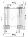
- FIG. 1shows a plan view of an organic light emitting diode display device according to a first exemplary embodiment of the present invention
- FIG. 2shows a simplified circuit diagram of unit pixels of the organic light emitting diode display device shown in FIG. 1 ;
- FIG. 3shows a signal timing diagram of the organic light emitting display device according to the first exemplary embodiment of the present invention
- FIGS. 4 to 6respectively show simplified circuit diagrams of unit pixels of organic light emitting diode display devices according to second to fourth exemplary embodiments of the present invention
- FIG. 7shows a signal timing diagram in the unit pixel of FIG. 6 ;
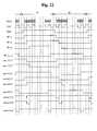
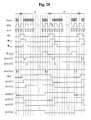
- FIGS. 8, 11 , 13 , 15 , 17 , 19 , 21 , 23 , 24 , 26 and 27respectively show scan drivers in organic light emitting diode display devices according to fifth to fifteenth exemplary embodiments;
- FIGS. 9, 12 , 14 , 16 , 18 , 20 , 22 , 25 , 28respectively show signal timing diagrams in the scan drivers of FIGS. 8, 11 , 13 , 15 , 17 , 19 , 21 , 24 , 26 ;
- FIG. 10shows a flip-flop used in a select scan driver of FIG. 8 ;
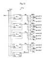
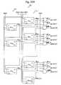
- FIG. 29shows a plan view of an organic light emitting diode display device according to a sixteenth exemplary embodiment of the present invention.
- FIGS. 30A and 30Brespectively show odd row and even row scan drivers in the organic light emitting diode display device according to the sixteenth exemplary embodiment.
- FIG. 31shows a signal timing diagram of the odd row scan driver of FIG. 30A .
- a display device and a driving method thereof according to exemplary embodiments of the present inventionwill be described in detail with reference to the drawings, and an organic light emitting diode display device using an organic light emitting diode as a light emitting element will be exemplified and described in the exemplary embodiments.
- FIG. 1shows a plan view of an organic light emitting diode display device according to a first exemplary embodiment of the present invention.
- the organic light emitting diode display deviceincludes a display area 100 seen as a screen to a user, a scan driver 200 , and a data driver 300 .
- the display area 100includes a plurality of data lines D 1 to D m , a plurality of select scan lines S 1 to S n , a plurality of emit scan lines Em 11 to Em 1n and Em 21 to Em 2n , and a plurality of unit pixels 110 .
- Each unit pixel 110includes two sub-pixels 111 and 112 which are arranged in a column direction.
- the data lines D 1 to D mare extended in a column direction and transmit data signals representing images to the corresponding unit pixels.
- the select scan lines S 1 to S nare extended in a row direction and transmit select signals for selecting corresponding lines to the select scan lines S 1 to S n in order to apply data signals to the unit pixels of the corresponding lines.
- the emit scan lines Em 11 to Em 1n and Em 21 to Em 2nare extended in a row direction and transmit emission control signals for controlling light emission of the respective sub-pixels 111 or 112 to the corresponding unit pixels 110 .
- the unit pixel 110is defined in an area where the select scan lines S 1 to S n and the data lines D 1 to D m are crossed.
- the scan lines S 1 to S nare coupled to the sub-pixels 111 and 112 in the respective unit pixels 110 .
- the scan driver 200sequentially transmits select signals to the select scan lines S 1 to S n in the respective subfields.
- the scan driver 200sequentially transmits emission control signals for controlling light emission of the sub-pixels 111 to the emit scan lines Em 11 to Em 1n in one subfield, and sequentially transmits emission control signals for controlling light emission of the sub-pixels 112 to the emit scan lines Em 21 to Em 2n in the other subfield.
- the data driver 300applies data signals corresponding to the pixels of lines to which select signals are applied to the data lines D 1 to D m each time the select signals are sequentially applied.
- the data driver 300applies data signals corresponding to the sub-pixels 111 in the one subfield, and applies data signals corresponding to the sub-pixels 112 in the other subfield.
- the scan driver 200 and the data driver 300are coupled to a substrate in which the display area 100 is formed.
- the scan driver 200 and/or the data driver 300may be installed directly on the substrate, and they may be substituted with a driving circuit which is formed on the same layer on the substrate as the layer on which scan lines, data lines, and transistors are formed.
- the scan driver 200 and/or the data driver 300may be installed in a chip format on a tape carrier package (TCP), a flexible printed circuit (FPC), or a tape automatic bonding unit (TAB) coupled to the substrate.
- TCPtape carrier package
- FPCflexible printed circuit
- TABtape automatic bonding unit
- FIG. 2shows a simplified circuit diagram of the unit pixels of the organic light emitting diode display device shown in FIG. 1 .
- the three unit pixels 110 ij , 110 i(j+1) , and 110 i(j+2) coupled to the scan line S i of the i th row (where ‘i’ is a positive integer less than or equal to ‘n’) and the data lines D j to D j+2 of the j th to (j+2) th columns (where ‘j’ is a positive integer less than or equal to ‘m ⁇ 2’)will be exemplified in FIG. 2 .
- the sub-pixelsare arranged in an order of R, G, and B along the row direction, and the same color sub-pixels are arranged along the column direction in FIG. 2 .
- the two sub-pixels 111 and 112 of the one unit pixel 100are coupled to one of the select scan lines S 1 to S n in common and have a pixel driver 115 in common, and the pixel driver 115 includes a driving transistor M 1 , a switching transistor M 2 , and a capacitor C 1 .
- the unit pixel 110 ij coupled to the i th select scan line S i and the j th data line D jincludes the pixel driver 115 , a switching unit, and two organic light emitting diodes OLED R1 and OLED R2 that emit red light.
- the switching unitincludes two emission control transistors M 3 a and M 3 b to selectively transmit a driving current from the pixel driver 115 to the two organic light emitting diodes OLED R1 and OLED R2 .
- the sub-pixels 111 ij and 112 ijrespectively include the two organic light emitting diodes OLED R1 and OLED R2 in the unit pixel 110 ij .
- the unit pixel 110 i(j+1) coupled to the i th select scan line S i and the (j+1) th data line D j+1 , and the unit pixel 110 i(j+2) coupled to the i th select scan line S i and the (j+2) th data line D j+2have the same structures as the unit pixel 110 ij .
- sub-pixels 111 i(j+1) and 112 i(j+1)respectively include two organic light emitting diodes OLED G1 and OLED G2 that emit green light in the unit pixel 110 i(j+1)
- sub-pixels 111 i(j+2) and 112 i(j+2)respectively include two organic light emitting diodes OLED B1 and OLED B2 that emit blue light in the unit pixel 110 i(j+2) .
- the driving transistor M 1has a source coupled to a power line for supplying a power supply voltage VDD, and a gate coupled to a drain of the switching transistor M 2 .
- the capacitor C 1is coupled between the source and the gate of the driving transistor M 1 .
- the switching transistor M 2having a gate coupled to the select scan line S i and a source coupled to the data line D j , transmits (or applies) the data signal converted to analog voltage (hereinafter, “data voltage”) provided by the data line D j in response to the select signal provided by the select scan line S i .
- the driving transistor M 1has a drain coupled to sources of the emission control transistors M 3 a and M 3 b, and gates of the emission control transistors M 3 a and M 3 b are coupled to the emit scan lines Em 1i and Em 2i , respectively. Drains of the emission control transistors M 3 a and M 3 b are coupled, respectively, to anodes of the organic light emitting diodes OLED R1 and OLED R2 , and a power supply voltage VSS is applied to cathodes of the organic light emitting diodes OLED R1 and OLED R2 .
- the power supply voltage VSS in the first exemplary embodimentis lower than the voltage VDD, and can be a negative voltage or a ground voltage. As shown in FIG. 2 , the unit pixels 110 i(j+1) and 110 i(j+2) have the same connecting structure as the unit pixel 110 ij .
- the one emit scan line Em 1i of the emit scan lines Em 1i and Em 2iis coupled to the gates of the transistors M 3 a respectively coupled to the organic light emitting diodes OLED R1 , OLED G1 and OLED B1
- the other emit scan line Em 2iis coupled to the gates of the transistors M 3 b respectively coupled to the organic light emitting diodes OLED R2, OLED G2 and OLED B2 .
- a low-level emission control signalis applied to the emit scan line Em 1i in one subfield of two subfields forming a field, and therefore, the transistor M 3 a is turned on. Then, a current I OLED as expressed in Equation 1 flows from the transistor M 1 to the organic light emitting diode so that the organic light emitting diodes OLED R1 , OLED G1 and OLED B1 emit light corresponding to the magnitude of the current I OLED .
- a low-level emission control signalis applied to the emit scan line Em 2i in the other subfield, and therefore, the transistor M 3 b is turned on.
- I OLED⁇ 2 ⁇ ( ⁇ V SG ⁇ - ⁇ V TH ⁇ ) 2 Equation ⁇ ⁇ 1
- ⁇is a constant determined by a channel width and a channel length of the transistor M 1
- V SGis a voltage between the source and the gate of the transistor M 1
- V THis a threshold voltage of the transistor M 1 .
- an upper line L 1is formed by the organic light emitting diodes OLED R1 , OLED G1 and OLED B1
- a lower line L 2is formed by the organic light emitting diodes OLED R2 , OLED G2 and OLED B2 .
- the organic light emitting diodes of the upper line L 1start emitting light in one subfield of the fields, and the organic light emitting diodes of the lower line L 2 start emitting light in the other subfield of the fields.
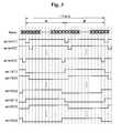
- FIG. 3A driving method of the organic light emitting diode display device according to the first exemplary embodiment of the present invention will be described in detail with reference to FIG. 3 .
- the select signal applied to the select scan line S iis depicted as ‘select[i]’
- the emission control signals applied to the emit scan lines Em 1i and Em 2iare depicted as ‘emit 1 [ i ]’ and ‘emit 2 [ i ]’, respectively.
- one fieldincludes two subfields 1 F and 2 F, and low-level select signals are sequentially applied to the select scan lines S 1 to S n in each subfield 1 F or 2 F.
- the two organic light emitting diodes of the unit pixel that share the select scan lineemit light during periods corresponding to subfields 1 F and 2 F, respectively.
- widths of low-level signals (e.g., pulses) of the emission control signals emit 1 [ i ] and emit 2 [ i ]are the same as periods corresponding to the subfields 1 F and 2 F, respectively.
- the first subfield 1 Fwhen a low-level select signal select[ 1 ] is applied to the select scan line S 1 on the first row, data voltages corresponding to the organic light emitting diodes OLED R1 , OLED G1 and OLED B1 of the unit pixels on the first row are applied to the corresponding data lines D 1 -D m .
- a low-level emission control signal emit 1 [ 1 ]is applied to the emit scan line Em 11 on the first row, and the emission control transistors M 3 a of the unit pixels on the first row are turned on.
- data voltages corresponding to the organic light emitting diodes OLED R1 , OLED G1 and OLED B1 of the unit pixels on the second roware applied to the corresponding data lines D 1 -D m .
- a low-level emission control signal emit 1 [ 2 ]is applied to the emit scan line Em 12 on the second row, and the emission control transistors M 3 a of the unit pixels on the second row are turned on.
- the organic light emitting diodes OLED R1 , OLED G1 and OLED B1 on the upper line L 1 of the second rowemit light in response to the low-level emission control signal emit 1 [ 2 ].
- the lightis emitted during the period in which the emission control signal emit 1 [ 2 ] is low-level.
- low-level select signals select[ 1 ] to select[n]are sequentially applied to the select scan lines S 1 to S n on the first to n th rows in the first subfield 1 F.
- the low-level select signal select[i]is applied to the select scan line S i on the i th row
- the data voltages corresponding to the organic light emitting diodes OLED R1 , OLED G1 and OLED B1 of the unit pixels on the i th roware applied to the corresponding data line D 1 to D m
- a low-level emission control signal emit 1 [ i ]is applied to the emit scan line Em 1i of the i th row.
- the organic light emitting diodes OLED R1 , OLED G1 and OLED B1which are formed on the upper line L 1 of the i th row, emit light during a period corresponding to the width of the low-level emission control signal emit 1 [ i].
- a low-level select signal select[ 1 ]is applied to the select scan line S 1 on the first row, and data voltages corresponding to the organic light emitting diodes OLED R2 , OLED G2 and OLED B2 of the unit pixels on the first row are applied to the corresponding data lines D 1 -D m .
- a low-level emission control signal emit 2 [ 1 ]is applied to the emit scan line Em 21 on the first row, and the emission control transistors M 3 b of the unit pixels on the first row are turned on. Then, the organic light emitting diodes OLED R2 , OLED G2 and OLED B2 on the lower line L 2 of the first row emit light during the period in which the emission control signal emit 2 [ 1 ] is low-level.
- a low-level select signal select[ 2 ]is applied to the select scan line S 2 on the second row, and data voltages corresponding to the organic light emitting diodes OLED R2 , OLED G2 and OLED B2 of the unit pixels on the second row are applied to the corresponding data lines D 1 -D m .
- a low-level emission control signal emit 2 [ 2 ]is applied to the emit scan line Em 22 on the second row, and the emission control transistors M 3 b of the unit pixels on the second row are turned on. Then, the organic light emitting diodes OLED R2 , OLED G2 and OLED B2 on the lower line L 2 of the second row emit light during the period in which the emission control signal emit 2 [ 2 ] is low-level.
- low-level select signals select[ 1 ] to select[n]are sequentially applied to the select scan lines S 1 to S n on the first to n th rows in the second subfield 2 F.
- the low-level select signal select[i]is applied to the select scan line S i on the i th row
- the data voltages corresponding to the organic light emitting diodes OLED R2 , OLED G2 and OLED B2 of the unit pixels on the i th roware applied to the corresponding data line D 1 to D m
- a low-level emission control signal emit 2 [ i ]is applied to the emit scan line Em 2i of the i th row.
- the organic light emitting diodes OLED R2 , OLED G2 and OLED B2which are formed on the lower line L 2 of the i th row, emit light in during a period corresponding to the width of the low-level emission control signal emit 2 [ i].
- one fieldis divided into the two subfields, and the subfields are sequentially driven in the organic light emitting diode display device driving method according to the first exemplary embodiment.
- the organic light emitting diodes formed on the upper line L 1 of the each rowstart emitting light in one subfield, and the organic light emitting diodes formed on the lower line L 2 of the each row start emitting light in the other subfield.
- the organic light emitting diodes of all sub-pixels formed on 2n lines of n rowscan emit light in the one field.
- the number of select scan lines and the number of pixel driverse.g., the transistors and the capacitors
- the number of integrated circuits for driving the select scan linescan be reduced, and the elements can be easily arranged in the unit pixel.
- the scan driver and the data driver of the interlace scan methodmay be applicable to those according to the first exemplary embodiment of the present invention because the lower lines L 2 are scanned after the upper lines L 1 are scanned in the first exemplary embodiment.
- the single scan methodis applicable to the organic light emitting diode display device in FIG. 3 , but the dual scan method may also be applicable to the organic light emitting diode display device according to the first exemplary embodiment by using two scan drivers.
- another scan method, in which the select scan signals are selectively applied to the plurality of select scan linesmay also be applicable to the organic light emitting diode display device according to the first exemplary embodiment.
- one sub-pixel 111 ij (including the organic light emitting diode OLED R1 ) of the unit pixel 110 ijis arranged on the upper side of the select scan line S i
- the other sub-pixel 112 ij (including the organic light emitting diode OLED R2 ) of the unit pixel 110 ijis arranged on the lower side of the select scan line S i
- the two sub-pixels 111 ij and 112 ijmay be arranged on the lower side (or the upper side) of the select scan line S i .
- FIG. 4shows a simplified circuit diagram of unit pixels 110 ij ′, 110 i(j+1) ′ and 110 i(j+2) ′ of an organic light emitting diode display device according to a second exemplary embodiment of the present invention.
- the organic light emitting diodes OLED R1 , OLED G1 and OLED B1are arranged below the pixel driver 115 to form the upper line L 1 ′, and the organic light emitting diodes OLED R2 , OLED G2 and OLED B2 are arranged below the upper line L 1 ′ to form the lower line L 2 ′.
- length of a wire for transmitting current from the pixel driver 115 to the organic light emitting diode OLED R2 , OLED G2 or OLED B2is longer than length of a wire for transmitting current from the pixel driver 115 to the organic light emitting diode OLED R1 , OLED G1 or OLED B1 .
- the brightness of the upper line L 1 ′may be different from the brightness of the lower line L 2 ′ by parasitic components present in the wire.
- the transistors M 1 , M 2 , M 3 a, and M 3 bare depicted as PMOS transistors in FIGS. 2 and 4 , but another conductive type of transistors may be applicable to the transistors M 1 , M 2 , M 3 a, and M 3 b.
- emission control transistors M 3 a and M 3 bare respectively controlled by the two emit scan lines Em 1i and Em 2i in the first and second exemplary embodiments, emission control transistors in other embodiments may be controlled by one emit scan line as shown in FIG. 5 .
- FIG. 5shows a simplified circuit diagram of unit pixels 110 ij ′′, 110 i(j+1) ′′ and 110 i(j+2) ′′ of an organic light emitting diode display device according to a third exemplary embodiment of the present invention.
- the unit pixel 110 ij ′′ according to the third exemplary embodimenthas the same structure as that according to the first exemplary embodiment, except for emission control transistors M 3 a ′ and M 3 b ′ and an emit scan line Em i .
- an emission control transistor M 3 a ′has the opposite conductive type to an emission control transistor M 3 b ′, and the emit scan line Em i on i th row is coupled to gates of the two emission control transistors M 3 a ′ and M 3 b ′.
- the emission control transistors M 3 a ′ respectively coupled to the organic light emitting diodes OLED R1 , OLED G1 and OLED B1 of the upper line L 1are depicted as PMOS transistors
- the emission control transistors M 3 b ′ coupled to the organic light emitting diodes OLED R2 , OLED G2 and OLED B2 of the lower line L 2are depicted as NMOS transistors.
- an emission control signal applied to the emit scan line Em ihas the same signal timing as the emission control signal emit 1 [ i ] shown in FIG. 3 .
- emission timings of the organic light emitting diodes OLED R1 , OLED G1 and OLED B1 coupled to the transistors M 3 a ′are the same as those of the first exemplary embodiment.
- emission control signal emit 2 [ i ]has an inverted waveform of the emission control signal emit 1 [ i ]
- the transistor M 3 b ′has the opposite conductive type to the transistor M 3 b shown in FIG. 2
- emission timings of the organic light emitting diodes OLED R2 , OLED G2 and OLED B2 coupled to the transistors M 3 b ′are the same as those of the first exemplary embodiment.
- the number of the emit scan lines Em i according to the third exemplary embodimentcan be reduced as compared with those according to the first and second exemplary embodiments.
- the two sub-pixelsshare the select scan line in the first to third exemplary embodiments, but three or more sub-pixels may share the select scan line in other embodiments.
- three emission control transistorsare coupled to the three organic light emitting diodes, respectively.
- the three emit scan linesmay be respectively coupled to gates of the three emission control transistors, and may respectively transmit (or apply) emission control signals for controlling the three emission control transistors.
- one fieldmay be divided into three subfields, and the three emission control transistors may be respectively turned on in the three subfields. Then, one row may be divided into the three lines, and the three lines may emit light in the three subfields, respectively.
- the sub-pixels having the same colorare coupled to the pixel driver 115 in the first to third exemplary embodiment, but the sub-pixels having different colors may be coupled to the pixel driver 115 .
- R organic light emitting diodemay be coupled to the upper side of the pixel driver 115 in the unit pixel 110 ij shown in FIG. 2
- G organic light emitting diodemay be coupled to the lower side of the pixel driver 115 .
- the driving voltages which are respectively transmitted from the driving transistors to the R, G, and B organic light emitting diodesare set to the different ranges.
- the ranges of the data voltages which are transmitted through the data lines to the driving transistorsmay be set to be different in R, G, and B sub-pixels, or the sizes of the driving transistors may be set to be different in the R, G, and B sub-pixels.
- the colors represented in the sub-pixels sharing the pixel driverare different, the data voltages corresponding to the sub-pixels having the different colors are respectively transmitted to the data line in the respective subfields. Then, the data voltage of the data driver is difficult to be optimized because the data voltage range of the data driver is not optimized to the sub-pixels having the same color and is optimized to or made suitable for the sub-pixels having different colors.
- each output of the data drivercan be optimized to the data voltage corresponding to each color. Accordingly, the data voltage transmitted to the one data line can be set to the voltage range corresponding to the one color, and the desired brightness can be represented in the respective sub-pixels. As a result, a white balance can be realized in the display area.
- the pixel driver using the switching and driving transistors and the capacitoris described in the first to third exemplary embodiments, but the plurality of sub-pixels may share a pixel driver which uses at least one transistor and/or at least one capacitor in addition to the switching and driving transistors to compensate variation of the threshold voltage of the driving transistor or the voltage drop. That is, since the driving current outputted from the pixel driver generally depends on the threshold voltage of the driving transistor in the unit pixel shown in FIG. 2 , the driving currents may be different if the threshold voltages of the driving transistors are different. Then, the brightness between the unit pixels may be different. A unit pixel which can compensate for a variation of the threshold voltage of the driving transistor will be described with reference to FIG. 6 .
- FIG. 6shows a simplified circuit diagram of a unit pixel of an organic light emitting diode display device according to a fourth exemplary embodiment of the present invention.
- the unit pixel coupled to the scan line S i of the i th row and the data line D jwill be exemplified in FIG. 6 .
- a scan line for transmitting a current select signalwill be referred to as a “current select scan line” and a scan line which has transmitted a select signal before the current select signal is transmitted will be referred to as a “previous select scan line.”
- a pixel driver 115 ′ of the unit pixel according to the fourth exemplary embodimentfurther includes a threshold voltage compensator for compensating a threshold voltage of a driving transistor.
- the threshold voltage compensatorincludes two transistors M 14 and M 15 , and a capacitor C 12 .
- transistors M 11 , M 12 , M 13 a, and M 13 bcorrespond to the transistors M 1 , M 2 , M 3 a, and M 3 b shown in FIG. 2 , respectively, and capacitors C 11 and C 12 correspond to the capacitor C 1 shown in FIG. 2 .
- a first electrode of the capacitor C 11is coupled to a power supply voltage VDD, and a second electrode of the capacitor C 11 is coupled to a first electrode of the capacitor C 12 .
- a second electrode of the capacitor C 12is coupled to a gate electrode of the driving transistor M 11 , and the switching transistor M 12 is coupled to the first electrode of the capacitor C 12 .
- the transistor M 14is coupled between gate and drain electrodes of the transistor M 11 , and diode-connects the transistor M 11 in response to the select signal of the previous select scan line S i ⁇ 1 .
- the transistor M 15is coupled between the power supply voltage VDD and the first electrode of the capacitor C 12 , and couples the first electrode of the capacitor C 12 to the power supply voltage VDD in response to the select signal of the previous select scan line S i ⁇ 1 .
- FIG. 7An operation of the unit pixel 115 ij ′ shown in FIG. 6 will be described with reference to FIG. 7 .
- a first subfield in which the organic light emitting diodes formed on the upper line L 1 are emitted by turn-on of the transistors M 13 awill be described only. Therefore, the emission control signal, which is applied to the emit scan line Em 2i and is high-level in the first subfield, is not shown in FIG. 7 .
- the transistors M 14 and M 15are turned on during a period in which the select signal select[i ⁇ 1] of the previous select scan line S i ⁇ 1 , is low-level, and the emission control signal emit 1 [ i ]′′ of the emit scan line Em 1i is high-level. Then, the transistor M 14 is diode-connected while the transistor M 13 a and M 13 b are turned off, and a voltage between the gate and source-electrodes of the transistor M 11 becomes the threshold voltage Vth of the transistor M 11 .
- a voltage at the gate electrode of the transistor M 11i.e., the second electrode of the capacitor C 12 , becomes “VDD+Vth” voltage.
- the transistor M 12is turned on and the transistors M 14 and M 15 are turned off during a period in which the select signal select[i] of the current select scan line S i is low-level, and the emit control signal emit 1 [ i ]′′ is high-level.
- the data voltage Vdatais applied to the first electrode of the capacitor C 12 through the switching transistor M 12 , a voltage at the second electrode of the capacitor C 12 is changed by the variation “Vdata ⁇ VDD” of the voltage at the first electrode of the capacitor C 12 . That is, the voltage at the second electrode of the capacitor C 12 becomes “Vdata+Vth” voltage, and therefore, the voltage between the gate and source electrodes of the transistor M 11 becomes “Vdata+Vth ⁇ VDD” voltage.
- the “Vdata+Vth ⁇ VDD” voltageis stored in the capacitors C 11 and C 12 .
- a unit pixelwhich can compensate the threshold voltage of the driving transistor by adding at least one transistor and/or at least one capacitor to the unit pixel of FIG. 2 may be used instead of the unit pixel shown in FIG. 6 .
- the low-level period of the emission control signalmay be set differently from the period shown in FIG. 3 .
- the low-level period of the emission control signalmay be set to be shorter than a period corresponding to the subfield. That is, the rising edge of the emission control signal may be set to be later than the rising edge of the select signal, and/or the falling edge of the emission control signal may be set to be faster (or earlier) than the rising edge of the select signal in the next subfield.
- the organic light emitting diode display device using the voltage programming methodis described in the first to fourth exemplary embodiments, but the above-described exemplary embodiments can be applicable to the organic light emitting diode display device using the current programming method.
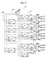
- scan driverse.g., the scan driver 200 of FIG. 1
- organic light emitting diode display deviceswill be described with reference to FIGS. 8 to 25 .
- FIG. 8shows a scan driver 200 a in an organic light emitting diode display device according to a fifth exemplary embodiment
- FIG. 9shows a signal timing diagram in the scan driver 200 a of FIG. 8
- FIG. 10shows a flip-flop used in the select scan driver 200 a of FIG. 8
- An inverted signal of a clock VCLKis depicted as /VCLK in FIG. 8 , and is not shown in FIG. 9 .
- the scan driver 200 aincludes two shift registers 210 a and 220 a.
- the shift register 210 aincludes (n+1) flip-flops FF 12 to FF 1(n+1) and n NAND gates NAND 11 to NAND 1n
- the shift register 220 aincludes n flip-flops FF 21 to FF 2n and n inverters INV 21 to INV 2n .
- a start signal VSP 1is inputted to the first flip-flop FF 11 , and an output signal SR 1i of the i th flip-flop FF 1i is inputted to the (i+1) th flip-flop FF 1(i+1) .
- the i th NAND gate NAND 1iperforms a NAND operation to the output signals SR 1i and SR 1(i+1) of the two adjacent flip-flops FF 1i and FF 1(i+1) and outputs a select signal select[i].
- a start signal VSP 2is inputted to the first flip-flop FF 21 , and an output signal of the i th flip-flop FF 2i is inputted to the (i+1) th flip-flop FF 2(i+1) .
- the output signal of the i th flip-flop FF 2iis the emission control signal emit 2 [ i ]
- the inverter INV 2iinverts the output signal of the i th flip-flop FF 2i to output the emission control signal emit 1 [ i].
- the flip-flops FF 1i and FF 2ioutput input signals (in) in response to a high-level clock (clk), and latch and output the input signals (in) of the high-level period of the clock (clk) in response to a low-level clock (clk). That is, the flip-flops F 1i and FF 2i output the input signals (in) of the high-level period of the inner clock (clk) during one clock VCLK cycle.
- the clock /VCLK or VCLK inverted to the clock VCLK or /VCLK, which are used in the flip-flop FF 1iare used in the flip-flops FF 1(i+1) adjacent to the flip-flop FF 1i .
- the flip-flops FF 1i that are located at odd-numbered positions in a longitudinal directionuse the clocks VCLK as inner clocks (clk).
- the flip-flops FF 1i that are located at even-numbered positions in the longitudinal directionuse the inverted clocks /VCLK as inner clocks (clk).
- the output signal SR 1i of the flip-flop FF 1iis inputted to the flip-flop FF 1(i+1) , the output signal SR 1(i+1) of the flip-flop FF 1(i+1) is shifted from the output signal SR 1i of the flip-flop FF 1i by a half clock VCLK cycle.
- the start signal VSP 1has a high-level signal (e.g., high-level pulse) in the high-level period of the one clock VCLK cycle in each of the subfields 1 F and 2 F, and the flip-flop FF 11 outputs the high-level signal during one clock VCLK cycle in each of the subfields 1 F and 2 F.
- the flip-flops FF 11 to FF 1(n+1)may sequentially output each output signal SR 1i by shifting the high-level signal by the half clock VCLK cycle.
- the NAND gate NAND 1iperforms a NAND operation of the output signals SR 1i and SR 1(i+1) of the flip-flops FF 1i and FF 1(i+1) , and outputs a low-level signal (e.g., low-level pulse) when both output signals SR 1i and SR 1(i+1) are high-level.
- a low-level signale.g., low-level pulse
- the output signal select[i] of the NAND gate NAND 1ihas a low-level signal during a period in which the both output signals SR 1i and SR 1(i+1) have the high-level signal in common in each of the subfields 1 F and 2 F.
- the output signal select[i+1] of the NAND gate NAND 1(i+1)is shifted from the output signal select[i] of the NAND gate NAND 1i by half the clock VCLK cycle. Therefore, the shift register 210 a may sequentially output each select signal select[i] by shifting the low-level signal by the half clock VCLK cycle.
- the flip-flop FF 2i of the shift register 220 ahas the same structure as the flip-flop FF 1i of the shift register 210 a except for the clocks VCLK and /VCLK. That is, the flip-flops FF 2i that are located at odd-numbered positions in the longitudinal direction use the inverted clocks /VCLK as inner clocks (clk), and the flip-flops FF 2i that are located at the even-numbered positions use the clocks VCLK as inner clocks (clk).
- the emission control signal emit 1 [ i+ 1]which is the output signal of the flip-flop FF 2(i+ 1) is shifted from the emission control signal emit 1 [ i ], which is the output signal of the flip-flop FF 2i , by the half clock VCLK cycle.
- the start signal VSP 2is high-level in the low-level period of all clock VCLK cycles in the subfield 1 F and is low-level in the low-level period of all clock VCLK cycles in the subfield 2 F.
- the emission control signal emit 2 [ 1 ]becomes high-level when the select signal select[ 1 ] becomes low-level in the first subfield 1 F, and becomes low-level when the select signal select[ 1 ] becomes low-level in the second subfield 2 F. Therefore, the shift register 220 a can sequentially output each emission control signal emit 2 [ i ], which becomes low-level together with the select signal select[i] in the second subfield 2 F, by shifting the half clock VCLK cycle.
- the shift register 220 acan sequentially output each emission control signal emit 1 [ i ], which becomes low-level together with the select signal select[i] in the first subfield 1 F, by shifting the half clock VCLK cycle.
- the flip-flop(e.g., FF 1i ) includes a clocked inverter 211 , and a latch including an inverter 212 and a clocked inverter 213 .
- the clocked inverter 211inverts an input signal (in) when the clock (clk) is high-level, and the inverter 212 inverts the output signal (/out) of the clocked inverter 211 .
- the output signal (out) of the inverter 212is the output signal of the flip-flop, and the input signal (/out) of the inverter 212 is the inverted signal to the output signal (out).
- the flip-flopcan output the input signal (in) when the clock (clk) is high-level, and latch and output the input signal (in) in the high-level period of the clock (clk) when the clock (clk) is low-level.
- the signal (/out) inverted to the output signal (out)is outputted from the flip-flop (e.g., FF 2i ) of the shift register 220 a. Therefore, the inverted output signal (/out) of the flip-flop of FIG. 10 may be used as the emission control signal emit 1 [ i ] of the first subfield 1 F, and the inverter INV 2i can be eliminated in the shift register 220 a.
- the signal having the high-level signal in the first subfield 1 Fis used as the start signal VSP 2 in FIGS. 8 and 9 , but a signal inverted to the start signal VSP 2 may be used as the start signal of the shift register 220 a.
- the output signal of the flip-flopbecomes the emission control signal emit 1 [ i ] of the first subfield 1 F
- the output signal of the inverter INV 2ibecomes the emission control signal emit 2 [ i ] of the second subfield 2 F.
- the emission control signal emit 1 [ i ] or emit 2 [ i ]is low-level when the select signal select[i] is low-level in the scan driver 200 a.
- This signal timingcan be applicable to the organic light emitting diode display device using the voltage programming method in which the data voltage is transmitted to the data line to be stored in the capacitor.
- the current from the driving transistorneeds to be blocked from the organic light emitting diodes when the data current are programmed to the pixel driver. That is, emission control signals emit 1 [ i ]′ and emit 2 [ i ]′ should be high-level when the select signal select[i] is low-level.
- this signal timingmay be applicable to the organic light emitting diode display device using the voltage programming method.
- FIG. 11shows a scan driver 200 b in an organic light emitting diode display device according to a sixth exemplary embodiment
- FIG. 12shows a signal timing diagram in the scan driver 200 b of FIG. 11
- the scan driver 200 b of FIGS. 11 and 12use the same clock VCLK as the scan driver 200 a shown in FIGS. 8 and 9 .
- the scan driver 200 bincludes the shift register 210 a for outputting the select signal select[i] and a shift register 220 b for outputting the emission control signals emit 1 [ i ]′ and emit 2 [ i ]′.
- the shift register 220 bincludes (n+1) flip-flops FF 31 to FF 3(n+1) , n NAND gates NAND 31 to NAND 3n , and n OR gates OR 31 to OR 3n .
- a NAND gate and an invertermay be used instead of the OR gate OR 3i .
- the clock VCLKis inputted to the flip-flops FF 3i , and the NAND gate NAND 3i performs a NAND operation between the output signals SR 3i and SR 3(i+1) of the flip-flops FF 3i and FF 3(i+1) to output the emission control signal emit 1 [ i ]′.
- the OR gate OR 3iperforms an OR operation between the output signals SR 3i and SR 3(i+1) of the flip-flops FF 3i and FF 3(i+1) to output the emission control signal emit 2 [ i]′.
- the start signal VSP 2 shown in FIG. 9is inputted to the flip-flop FF 3i . Therefore, the output signal SR 3i of the flip-flop FF 3i becomes high-level when the select signal select[i] becomes low-level in the first subfield 1 F, and becomes low-level when the select signal select[i] becomes low-level in the second subfield 2 F. Since the NAND gate NAND 3i outputs the low-level signal while both the output signal SR 3i and SR 3(i+1) of the flip-flops FF 3i and FF 3(i+1) are high-level, the emission control signal emit 1 [ i ]′ becomes low-level when the select signal select[i] becomes high-level in the first subfield 1 F.
- the OR gate OR 3ioutputs the high-level signal while both the output signal SR 3i and SR 3(i+1) of the flip-flops FF 3i and FF 3(i+1) are low-level, the emission control signal emit 2 [ i ]′ becomes low-level when the select signal select[i] becomes high-level in the second subfield 2 F.
- emission control signals emit 1 [ i ]′ and emit 2 [ i ]′are high-level in the sixth exemplary embodiment when the select signal select[i] has the low-level signal.
- emission control signals emit 1 [ i ]′′ and emit 2 [ i ]′′may be high-level when the previous and current select signals select[i ⁇ 1] and select[i] have the low-level signals. This exemplary embodiment will be described with reference to FIGS. 13 and 14 .
- FIG. 13shows a scan driver 200 c in an organic light emitting diode display device according to a seventh exemplary embodiment
- FIG. 14shows a signal timing diagram of the scan driver 200 c shown in FIG. 13
- the scan driver 200 c of FIGS. 13 and 14use the same clock VCLK as the scan driver 200 a shown in FIGS. 8 and 9 .
- the scan driver 200 cincludes the shift register 210 a for outputting the select signal select[i] and a shift register 220 c for outputting the emission control signals emit 1 [ i ]′′ and emit 2 [ i ]′′.
- the shift register 220 cincludes n flip-flops FF 41 to FF 4n , n inverters INV 41 to INV 4n , and 2n NOR gates NOR 11 to NOR 1n , and NOR 41 to NOR 4n .
- the flip-flops FF 41 to FF 4n and the inverters INV 41 to INV 4nhave the same structure as the flip-flops FF 21 to FF 2n and the inverters INV 21 to INV 2n of FIG. 8 except for the clocks VCLK and /VCLK. That is, the flip-flop FF 4i uses the clock VCLK or /VCLK inverted to the clock /VCLK or VCLK of the flip-flop FF 2i shown in FIG. 8 .
- the NOR gate NOR 1iperforms a NOR operation between the output signal SR 1i of the flip-flop FF 1i and the inverted output signal /SR 4i of the flip-flop FF 4i to output the emission control signal emit 1 [ i ]′′ in the first subfield 1 F.
- the NOR gate NOR 4iperforms a NOR operation between the output signals SR 1i and SR 4i of the flip-flops FF 1i and FF 4i to output the emission control signal emit 2 [ i ]′′ in the second subfield 2 F.
- a start signal VSP 2 ′is high-level in the high-level period of the clock VCLK in the first subfield 1 F and is low-level in the high-level period of the clock VCLK in the second subfield 2 F.
- the output signal SR 4i of the flip-flop FF 4ihas the high-level signal during a period corresponding to the first subfield 1 F and has the low-level signal during a period corresponding to the second subfield 2 F.
- the output signal SR 4i of the flip-flop FF 4ibecomes high-level when the output signal SR 1i of the flip-flop FF 1i becomes high-level in the first subfield 1 F, and becomes low-level when the output signal SR 1i of the flip-flop FF 1i becomes high-level in the second subfield 2 F.
- the output signal emit 1 [ i ]′′ of the NOR gate NOR 1ibecomes low-level together with the output signal SR 1i in the first subfield 1 F and becomes high-level together with the output signal SR 1i in the second subfield 2 F.
- the output signal emit 2 [ i ]′′ of the NOR gate NOR 4ibecomes low-level together with the output signal SR 1i in the second subfield 2 F and becomes high-level together with the output signal SR 4i in the first subfield 1 F. Therefore, the emission control signals emit 1 [ i ]′′ and emit 2 [ i ]′′ are high-level when the previous and current select signals select[i ⁇ 1] and select[i] have the low-level signals.
- the emission control signals emit 1 [ i ]′′ and emit 2 [ i ]′′ shown in FIG. 14may be generated from the scan driver shown in FIG. 11 .
- This exemplary embodimentwill be described with reference to FIGS. 15 and 16 .
- FIG. 15shows a scan driver 200 d in an organic light emitting diode display device according to an eight exemplary embodiment
- FIG. 16shows a signal timing diagram of the scan driver 200 d shown in FIG. 15 .
- the scan driver 200 dincludes the shift register 210 a for outputting the select signal select[i] and a shift register 220 d for outputting the emission control signals emit 1 [ i ]′′ and emit 2 [ i ]′′.
- the shift register 220 dfurther includes a flip-flop FF 30 before the flip-flop FF 31 , which is different from the shift register 220 b of FIG. 11 , and a start signal VSP 2 ′′ is inputted to the flip-flop FF 30 .
- the flip-flop FF 30receives the clock VCLK as the inner clock (clk).
- the i th NAND gate NAND 3iperforms a NAND operation between the output signals SR 3(i ⁇ 1) and SR 3(i+1) of the (i ⁇ 1) th and (i+1) th flip-flops FF 3(i ⁇ 1) and FF 3(i+1) to output the emission control signal emit 1 [ i ]′′.
- the i th OR gate OR 3iperforms an OR operation between the output signals SR 3(i ⁇ 1) and SR 3(i+1) of the (i ⁇ 1) th and (i+1) th flip-flops FF 3(i ⁇ 1) and FF 3(i+1) to output the emission control signal emit 2 [ i]′′.
- the start signal VSP 2 ′′is high-level when the clock VCLK is high-level in the first subfield 1 F, and is low-level when the clock VCLK is high-level in the second subfield 2 F. Then, the output signal SR 3i of the flip-flop FF 3i is same as that SR 3i shown in FIG. 12 . Therefore, the emission control signals emit 1 [ i ]′′ and emit 2 [ i ]′′ are high-level when the previous and current select signal select[i ⁇ 1] and select[i] have the low-level signals.
- the select signals and the emission control signalsare generated from the two shift registers each including the plurality of flip-flops.
- exemplary embodimentwhich may reduce the number of the flip-flops compared to these exemplary embodiments, will be described.
- FIG. 17shows a scan driver 200 e in an organic light emitting diode display device according to a ninth exemplary embodiment
- FIG. 18shows a signal timing diagram of the scan driver 200 e shown in FIG. 17
- a clock VCLK′ used in the scan driver 200 e of FIGS. 17 and 18has twice the period of the clock VCLK of FIGS. 8 to 16 , and the inverted clock /VCLK′ is not shown in FIG. 18 .
- the scan driver 200 eincludes a shift register 210 e for outputting the select signal select[i] and a shift register 220 e for outputting the emission control signals emit 1 [ i ]′′ and emit 2 [ i ]′′.
- the shift register 210 eincludes ((n/2)+1) flip-flops FF 51 to FF 5(n/2+1) , n NAND gates NAND 51 to NAND 5(n/2) , and NAND 61 to NAND 6(n/2) , and the shift register 220 e includes (n/2) flip-flops FF 61 to FF 6(n/2) , and n OR gates OR 51 to OR 5(n/2) , and OR 61 to OR 6(n/2) (where ‘n’ is assumed to an even number).
- the clocks VCLK′ and /VCLK′ of the flip-flop FF 5(j+1)are inverted to the clocks /VCLK′ and VCLK′ of the adjacent flip-flops FF 5j in the shift register 210 e (where ‘j’ is a positive integer less than or equal to ‘n/2’), and the clock VCLK′ is inputted to the flip-flop FF 51 as the inner clock (clk). As shown in FIG.
- the flip-flops FF 51 to FF 5(n/2+1)may sequentially output each output signal SR 5i by shifting the high-level signal by the half clock VCLK′ cycle.
- the output signal SR 5ihas the high-level signal during one clock VCLK′ cycle in each of the subfields 1 F and 2 F.
- the j th NAND gate NAND 5jperforms a NAND operation of the output signals SR 5j and SR 5(j+1) of the flip-flops FF 5j and FF 5(j+1) , and the inverted clock /VCLK to output the (2j ⁇ 1) th select signal select[2j ⁇ 1]. Therefore, the select signal select[2j ⁇ 1] has the low-level signal during a low-level period of the clock VCLK of a period in which the both output signals SR 5j and SR 5(j+1) are high-level.
- the j th NAND gate NAND 6jperforms the NAND operation of the output signals SR 5j and SR 5(j+1) of the flip-flops FF 5j and FF 5(j+1) , and the clock VCLK to output the (2j) th select signal select[ 2 j ]. Therefore, the select signal select[ 2 j ] has the low-level signal during a high-level period of the clock VCLK of the period in which the both output signals SR 5j and SR 5(j+1) are high-level.
- the clocks VCLK′ and /VCLK′ of the flip-flop FF 6(j+1)are inverted to the clocks /VCLK′ and VCLK′ of the adjacent flip-flops FF 6j in the shift register 212 e, and the inverted clock /VCLK′ is inputted to the flip-flop FF 61 as the inner clock (clk).
- the flip-flops FF 61 to FF 6(n/2)may sequentially output each output signal SR 6i by shifting the high-level signal by the half clock VCLK′ cycle.
- the output signal SR 6ihas the high-level signal during a period corresponding to the first subfield 1 F.
- the j th OR gate OR 5jperforms an OR operation of the output signal SR 5j of the flip-flop FF 5j and the inverted output signal /SR 6j of the flip-flop FF 6j to output the (2j ⁇ 1) th and (2j) th emission control signals emit 1 [ 2 j ⁇ 1]′′ and emit 1 [ 2 j ]′′ (shown as emit 1 [ 2 j ⁇ 1, 2 j ] in FIG. 17 ) in the first subfield 1 F.
- the emission control signals emit 1 [ 2 j ⁇ 1]′′ and emit 1 [ 2 j ]′′have the low-level signal during a period in which the both output signal SR 5j of the flip-flop FF 5j and inverted output signal /SR 6j of the flip-flop FF 6j are low-level.
- the j th OR gate OR 6jperforms the OR operation of the output signal SR 5j of the flip-flop FF 5j and the output signal SR 6j of the flip-flop FF 6j to output the (2j ⁇ 1) th and (2j) th emission control signals emit 2 [ 2 j ⁇ 1]′′ and emit 2 [ 2 j ]′′ (shown as emit 2 [ 2 j ⁇ 1, 2 j ] in FIG.
- the emission control signals emit 2 [ 2 j ⁇ 1]′′ and emit 2 [ 2 j ]′′have the low-level signal during a period in which the both output signals SR 5j and SR 6j of the flip-flops FF 5j and FF 6j are low-level.
- the emission control signals emit 1 [ 2 j ⁇ 1]′′ and emit 2 [ 2 j ⁇ 1]′′are high-level when the previous and current select signals select[ 2 j ⁇ 2] and select[ 2 j ⁇ 1] have the low-level signals
- the emission control signals emit 1 [ 2 j ]′′ and emit 2 [ 2 j ]′′are high-level when the previous and current select signals select[ 2 j ⁇ 1] and select[ 2 j ] have the low-level signal.
- a scan driver 200 f for outputting the emission control signals emit 1 [ i ] and emit 2 [ i ] shown in FIG. 9will be described with reference to FIGS. 19 and 20 .
- FIG. 19shows the scan driver 200 f in an organic light emitting diode display device according to a tenth exemplary embodiment
- FIG. 20shows a signal timing diagram of the scan driver 200 f shown in FIG. 19 .
- the scan driver 200 fincludes (n+1) flip-flops FF 71 to FF 7(n+1) , n XNOR gates XNOR 71 to XNOR 7n , and n inverters INV 71 to INV 7n , and operates as a shift register.
- the flip-flops FF 71 to FF 7(n+1) and the n inverters INV 71 to INV 7nhave the same structure as the flip-flops FF 11 to FF 1(n+1) and the n inverters INV 21 to INV 2n shown in FIG. 8 .
- the flip-flops FF 71 to FF 7(n+1)use the clock VCLK and the start signal VSP 2 shown in FIG. 9 .
- an output signal SR 7i of the flip-flop FF 7iis same as the emission control signal emit 1 [ i ] of the first subfield 1 F, and the output signal of the inverter INV 7i is same as the emission control signal emit 2 [ i ] of the second subfield 2 F.
- the inverted output signal (/out) of the flip-flop FF 7imay be used as the emission control signal emit 2 [ i ] instead of the output signal of the inverter INV 7i .
- the XNOR gate XNOR 7iperforms XNOR operation between the output signals SR 7i and SR 7(i+1) of the flip-flops FF 7i and FF 7(i+1) to output the select signal select[i]. That is, the XNOR gate XNOR 7i outputs the low-level select signal select[i] while the output signals SR 7i and SR 7(i+1) of the flip-flops FF 7i and FF 7(i+1) have the different levels.
- the select signal select[i]has the low-level signals during a period corresponding to the half clock VCLK cycle from the falling edge of the output signal SR 7i and a period corresponding to the half clock VCLK cycle from the rising edge of the output signal SR 7i .
- the emission control signals emit 1 [ i ] and emit 2 [ i ]become low-level together with the select signal select[i] in the first and second subfields 1 F and 2 F, respectively.
- scan drivers 200 g and 220 h for outputting the emission control signals emit 1 [ i ]′ and emit 2 [ i ]′ shown in FIG. 12will be described with reference to FIGS. 21 to 23 .
- FIG. 21shows the scan driver 200 g in an organic light emitting diode display device according to an eleventh exemplary embodiment
- FIG. 22shows a signal timing diagram of the scan driver 200 g shown in FIG. 21 .
- the scan driver 200 ghas the same structure as the scan driver 200 f of FIG. 19 except that the emission control signals emit 1 [ i ]′ and emit 2 [ i ]′ are generated from a NAND gate NAND 7i and an OR gate OR 7i .
- the i th NAND gate NAND 7iperforms a NAND operation between the output signals SR 7i and SR 7(i+1) of the flip-flops FF 7i and FF 7(i+1) to output the emission control signal emit 1 [ i ]′ of the first subfield 1 F
- the i th OR gate OR 7iperforms an OR operation between the output signals SR 7i and SR 7(i+1) of the flip-flops FF 7i and FF 7(i+1) to output the emission control signal emit 2 [ i ]′ of the second subfield 2 F.
- the emission control signals emit 1 [ i ]′ and emit 2 [ i ]′are at high-level in a period corresponding to the low-level signal of the select signal select[i]
- the emission control signals emit 1 [ i ]′ and emit 2 [ i ]′ shown in FIG. 22can be outputted.
- FIG. 23shows the scan driver 200 h in an organic light emitting diode display device according to a twelfth exemplary embodiment.
- the scan driver 200 hhas the same structure as the scan driver 200 g of FIG. 21 except that the select signal select[i] are generated from a NAND gate NAND 8i .
- the two emission control signal emit 1 [ i ]′ and emit 2 [ i ]′have high-levels during a period in which the select signal select[i] has low-level. Therefore, the select signal select[i] can be generated by the NAND operation of the emission control signals emit 1 [ i ]′ and emit 2 [ i ]′ which is performed by the NAND gate NAN D 8i .
- a scan driver 200 i for outputting the emission control signals emit 1 [ i ]′′ and emit 2 [ i ]′′ shown in FIG. 14will be described with reference to FIGS. 24 to 26 .
- FIG. 24shows the scan driver 200 i in an organic light emitting diode display device according to a thirteenth exemplary embodiment
- FIG. 25shows a signal timing diagram of the scan driver 200 i shown in FIG. 24 .
- the scan driver 200 i of FIG. 24further includes 2n OR gates OR 11 to OR 1n and OR 21 to OR 2n in addition to the elements of the scan driver 200 g of FIG. 21 , and the flip-flops FF 71 to FF 7n are not shown in FIG. 24 .
- the i th OR gates OR 1i and OR 2i(i ⁇ 1) th and i th NAND gates NAND 7(i ⁇ 1) and NAND 7i , (i ⁇ 1) th and i th OR gates OR 7(i ⁇ 1) and OR 7i , and i th XNOR gate XNOR 7i are shown in FIG. 24 .
- the signals SR 7(i ⁇ 1) , SR 7i , and SR 7(i+1)respectively correspond to the output signals of the flip-flops FF 7(i ⁇ 1) , FF 7i , and FF 7(i+1)
- signals A i and B irespectively correspond to the emission control signals emit 1 [ i ]′ and emit 2 [ i ]′ of the scan driver 200 g shown in FIG. 21 .
- the OR gate OR 1iperforms an OR operation of the signals A i ⁇ 1 and A i to output the emission control signals emit 1 [ i ]′′ during a period in which the both signals A i ⁇ 1 and A i are low-level.
- the OR gate OR 2iperforms an OR operation of the signals B 1 ⁇ 1 and B i to output the emission control signals emit 2 [ i ]′′ during a period in which the both signals B i ⁇ 1 and B i are low-level.
- These emission control signals emit 1 [ i ]′′ and emit 2 [ i ]′′are same as those shown in FIG. 14 .
- the low-level periods of the emission control signals emit 1 [ i ]′′ and emit 2 [ i ]′′may be controlled by an integral multiple of the half clock VCLK cycle.
- FIG. 26shows a scan driver 200 j in an organic light emitting diode display device according to a fourteenth exemplary embodiment.
- the scan driver 200 jincludes a NAND gate NAND 8i instead of the XNOR gate XNOR 7i in the scan driver 200 i of FIG. 24 .
- the i th NAND gate NAND 8iperforms a NAND operation of the output signal A i of the i th NAND gate NAND 7i and the output signal B i of the i th OR gate OR 7i to output the select signal select[i] as described in reference to FIG. 23 .
- the width of the low-level signal of the select signal select[i]is same as the half clock VCLK cycle. That is, the rising edge of the select signal select[i ⁇ 1] corresponds to the falling edge of the select signal select[i]. In other embodiment, however, the falling edge of the select signal select[i] may be apart from the rising edge of the select signal select[i ⁇ 1]. That is, the width of the low-level signal of the select signal select[i] may be shorter than the half clock VCLK cycle.
- FIGS. 27 and 28One such exemplary embodiment will be described with reference to FIGS. 27 and 28 .
- FIG. 27shows a scan driver 200 k in an organic light emitting diode display device according to a fifteenth exemplary embodiment
- FIG. 28shows a signal timing diagram of the scan driver 200 k shown in FIG. 27 .
- the low-level signal widthe.g., low-level pulse width
- the scan driver 200 khas the same structure as the scan driver 200 a of FIGS. 8 and 9 except for a clip signal CLIP, and NAND gates NAND 11i (i.e., NAND 111 to NAND 11n ), to which the clip signal CLIP is applied in addition to the output signals SR 1i and SR 1(i+1) .
- the clip signal CLIPhas a cycle corresponding to the half clock VCLK cycle, and has the low-level signal whose width is shorter than the half clock VCLK cycle.
- the low-level period of the clip signal CLIPincludes the falling edge or the rising edge of the clock VCLK.
- the NAND gate NAND 11ioutputs the low-level signal of the select signal select[i]′ (i.e., one of select signals select[ 1 ]′ to select[n]′) during a period in which the clip signal CLIP is high-level. That is, the falling edge of the select signal select[i]′ is apart from the rising edge of the select signal select[i ⁇ 1]′ by the low-level signal width (e.g., low-level pulse width) of the clip signal CLIP.
- the low-level signal widthe.g., low-level pulse width
- FIGS. 27 and 28may also be applicable to the other exemplary embodiments described above.
- the scan drivermay be divided into a scan driver for driving the unit pixels formed on the odd row (hereinafter, “an odd row scan driver”) and a scan driver for driving the unit pixels formed on the even row (hereinafter, “an even row scan driver”).
- an odd row scan driverfor driving the unit pixels formed on the odd row
- an even row scan driverfor driving the unit pixels formed on the even row
- FIG. 29shows a plan view of an organic light emitting diode display device according to a sixteenth exemplary embodiment of the present invention
- FIGS. 30A and 30Brespectively show odd row and even row scan drivers 201 and 202 in the organic light emitting diode display device according to the sixteenth exemplary embodiment
- FIG. 31shows a signal timing diagram of the odd row scan driver 201 shown in FIG. 30A .
- the organic light emitting diode display devicehas the same structure as that of FIG. 1 except for the scan drivers 201 and 202 .
- the odd row scan driver 201is formed on one side of the display area 100 , and sequentially transmits the select signals select[ 2 j ⁇ 1] to the odd-numbered select scan lines S 2j ⁇ 1 (where ‘j’ is a positive integer less than or equal to n/2).
- the even row scan driver 202is formed on the other side of the display area 100 , and sequentially transmits the select signals select[ 2 j ] to the even-numbered select scan lines S 2j .
- the odd row scan driver 201sequentially transmits emission control signals emit 1 [ 2 j ⁇ 1]′′ to the odd-numbered emit scan lines Em 1(2j ⁇ 1) in the first subfield 1 F, and sequentially transmits emission control signals emit 2 [ 2 j ⁇ 1]′′ to the odd-numbered emit scan lines Em 2(j ⁇ 1) in the second subfield 2 F.
- the even row scan driver 202sequentially transmits emission control signals emit 1 [ 2 j ]′′ to the even-numbered emit scan lines Em 1(2j) in the first subfield 1 F, and sequentially transmits emission control signals emit 2 [ 2 j ]′′ to the even-numbered emit scan lines Em 2(2j) in the second subfield 2 F.
- the odd row scan driver 201has a structure in which NAND gates NAND 61 to NAND 6(n/2) for even-numbered select signals are eliminated from the scan driver 200 e shown in FIG. 17 .
- the odd row scan driver 201includes a shift register 211 for outputting the odd-numbered select signals select[ 2 j ⁇ 1] and a shift register 221 for outputting the odd-numbered emission control signals emit 1 [ 2 j ⁇ 1]′′ and emit 2 [ 2 j ⁇ 1]′′.
- the shift register 211includes ((n/2)+1) flip-flops FF 81 , FF 83 , . . .
- the shift register 221includes (n/2) flip-flops FF 91 , FF 93 , . . . , FF 9(n ⁇ 1) , and n OR gates OR 81 , OR 83 , . . . , OR 8(n ⁇ 1) , and OR 91 , OR 93 , . . . , OR 9(n ⁇ 1) .
- the even row scan driver 202has a structure in which the NAND gates NAND 51 to NAND 5(n/2) for odd-numbered select signals are eliminated from the scan driver 200 e shown in FIG. 17 .
- the even row scan driver 202includes a shift register 212 for outputting the even-numbered select signal select[ 2 j ] and a shift register 222 for outputting the even-numbered emission control signals emit 1 [ 2 j ]′′ and emit 2 [ 2 j ]′′.
- the shift register 212includes ((n/2)+1) flip-flops FF 82 FF 84 , . . .
- the shift register 212includes (n/2) flip-flops FF 92 , FF 94 , . . . , FF 9n , and n OR gates OR 82 , OR 84 , . . . , OR 8n , and OR 92 , OR 94 , . . . , OR 9n .
- the start signal VSP 1 ′ shown in FIG. 18is inputted to the flip-flops FF 81 and FF 82
- the start signal VSP 2 ′′ shown in FIG. 18is inputted to the flip-flops FF 91 and FF 92 .
- the NAND gate NAND 9(2j ⁇ 1) of the scan driver 201performs a NAND operation of the output signals SR 8(2j ⁇ 1) and SR 8(2j+1) of the flip-flops FF 8(2j ⁇ 1) and FF 8(2j+1) and the clock VCLK to output the (2j ⁇ 1) th select signal select[ 2 j ⁇ 1].
- the NAND gate NAND 9(2j) of the scan driver 202performs a NAND operation of the output signals SR 8(2j) and SR 8(2j+2) of the flip-flops FF 8(2j) and FF 8(2j+2) and the inverted clock /VCLK to output the (2j) th select signal select[ 2 j].
- the OR gate OR 8(2j ⁇ 1)performs an OR operation of the output signal SR 8(2j ⁇ 1) of the flip-flop FF 8(2j ⁇ 1) and the inverted output signal /SR 9(2j ⁇ 1) of the flip-flop FF 9(2j ⁇ 1) to output the (2j ⁇ 1) th emission control signal emit 1 [ 2 j ⁇ 1]′′
- the OR gate OR 9(2j ⁇ 1)performs an OR operation of the output signals SR 8(2j ⁇ 1) and SR 9(2j ⁇ 1) of the flip-flops FF 8(2j ⁇ 1) and FF 9(2j ⁇ 1) to output the (2j ⁇ 1) th emission control signal emit 2 [ 2 j ⁇ 1]′′.
- the OR gate OR 8(2j)performs an OR operation of the output signal SR 8(2j) of the flip-flop FF 8(2j) and the inverted output signal /SR 9(2j) of the flip-flop FF 9(2j) to output the (2j) th emission control signal emit 1 [ 2 j ]′′
- the OR gate OR 9(2j)performs an OR operation of the output signals SR 8(2j) and SR 9(2j) of the flip-flops FF 8(2j) and FF 9(2j) to output the (2j) th emission control signal emit 2 [ 2 j]′′.
- FIGS. 29 to 31The principles of the exemplary embodiment described in FIGS. 29 to 31 may also be applicable to the other exemplary embodiments described above.
- one or more buffersmay be formed between the display area 100 and the scan driver 200 (or the scan drivers 201 and 202 ).
- one or more level shifterswhich change the levels of the select signals and the emission control signals may also be formed between the display area 100 and the scan driver 200 (or the scan drivers 201 and 202 ).
- the plurality of sub-pixelsshare the select scan line and the pixel driver in the unit pixel.
- the sub-pixelscan be easily arranged in the unit pixel, and the aperture ratio of the unit pixel can be improved.
- the number of the select scan linesis reduced compared to that of the number of the row lines, the number of the output terminals and the dimension of the scan driver can be reduced. Further, since the dimension of the scan driver is reduced, the non-emission area can be reduced when the scan driver and the unit pixels are formed on the same substrate.
- the number of the flip-flopscan be reduced in the scan driver for outputting the select signals and the emission control signals of the first and second subfields.
Landscapes
- Engineering & Computer Science (AREA)
- Computer Hardware Design (AREA)
- General Physics & Mathematics (AREA)
- Theoretical Computer Science (AREA)
- Physics & Mathematics (AREA)
- Environmental Sciences (AREA)
- Life Sciences & Earth Sciences (AREA)
- Animal Husbandry (AREA)
- Biodiversity & Conservation Biology (AREA)
- Control Of Indicators Other Than Cathode Ray Tubes (AREA)
- Control Of El Displays (AREA)
- Electroluminescent Light Sources (AREA)
- Shift Register Type Memory (AREA)
Abstract
Description
- This application claims priority to and the benefit of Korean Patent Application No. 10-2005-0000759 filed on Jan. 5, 2005 in the Korean Intellectual Property Office, the entire content of which is incorporated herein by reference.
- 1. Field of the Invention
- The present invention relates to a display device and a driving method thereof, and more particularly, to an organic light emitting diode (OLED) display device and a driving method thereof.
- 2. Description of the Related Art
- In general, the organic light emitting diode display device is a display device for electrically exciting phosphorous organic matter and emitting light. The organic light emitting diode display device drives organic light emission cells arranged in a matrix format to represent images. An organic light emission cell having a diode characteristic is referred to as an organic light emitting diode (OLED) and has a structure including an anode electrode layer, an organic thin film, and a cathode electrode layer. Holes and electrons injected through the anode electrode and the cathode electrode are combined on the organic thin film, and emit light. The organic light emission cell emits different amounts of light according to injected amounts of electrons and holes, that is, depending on the applied current.
- In a display device such as the organic light emitting diode display device, a pixel includes a plurality of sub-pixels each of which has one of a plurality of colors (e.g., primary colors of light), and colors are represented through combinations of the colors emitted by the sub-pixels. In general, a pixel includes a sub-pixel for displaying red (R), a sub-pixel for displaying green (G), and a sub-pixel for displaying blue (B), and the colors are displayed by combinations of red, green, and blue (RGB) colors. Generally, the sub-pixels are arranged in an order of R, G, and B along a row direction.
- Each sub-pixel in the organic light emitting diode display device includes a driving transistor for driving the organic light emitting diode, a switching transistor, and a capacitor. Also, each sub-pixel has a data line for transmitting (or applying) a data signal, and a power line for transmitting (or applying) a power supply voltage. Therefore, many wires are required for transmitting (or applying) voltages or signals to the transistors and capacitors formed at each pixel. It is difficult to arrange such wires in the pixel, and the aperture ratio corresponding to a light emission area of the pixel is reduced.
- One exemplary embodiment of the present invention provides a display device for improving an aperture ratio.
- Another exemplary embodiment of the present invention provides a display device for simplifying the arrangement of wires and elements in unit pixels.
- Still another exemplary embodiment of the present invention provides a display device for reducing a number of select scan lines.
- Further, another exemplary embodiment of the present invention provides a scan driver for reducing a number of flip-flops.
- In one aspect of the present invention, a display device including a plurality of unit pixels, a plurality of data lines, a plurality of select scan lines, a plurality of emit scan lines, and a scan driver is provided. A field is divided into a plurality of subfields. The plurality of unit pixels are arranged in rows and display an image during the field. Each of the unit pixels includes a plurality of light emitting elements arranged in a column direction. The plurality of data lines extend in the column direction, and transmit data signals. The plurality of select scan lines extend in a row direction and transmit select signals, and each of the select scan lines is coupled to a corresponding one of the rows of the unit pixels. The plurality of emit scan lines transmit emission control signals, and each of the emit scan lines is coupled to a corresponding one of the rows of the unit pixels. The scan driver applies the select signals to the select scan lines, and applies the emission control signals to the emit scan lines, in each of the plurality of subfields. At least one of the unit pixels uses a corresponding one of the data signals in response to a first signal of a corresponding one of the select signals, and each of the plurality of light emitting elements of the at least one of the unit pixels emits light in response to an emit signal of a corresponding one of the emission control signals in a corresponding one of the subfields.
- In another aspect of the present invention, a display device including a plurality of unit pixels, a plurality of data lines, a plurality of select scan lines, a plurality of emit scan lines, a first scan driver, and a second scan driver is provided. A field is divided into a plurality of subfields. The plurality of unit pixels are arranged in rows and display an image during the field. Each of the unit pixels includes a plurality of light emitting elements arranged in a column direction. The plurality of data lines extend in the column direction and transmit data signals. The plurality of select scan lines extend in a row direction and transmit select signals, and each of the select scan lines is coupled to a corresponding one of the rows of the unit pixels. The plurality of emit scan lines transmit emission control signals, and each of the emit scan lines is coupled to a corresponding one of the rows of the unit pixels. The first scan driver applies the select signals to the select scan lines of a first row group from among the rows of the unit pixels and applies the emission control signals to the emit scan lines of the first row group, in each of the plurality of subfields. The second scan driver applies the select signals to the select scan lines of a second row group from among the rows of the unit pixels and applies the emission control signals to the emit scan lines of the second row group, in each of the plurality of subfields. At least one of the unit pixels uses a corresponding one of the data signals in response to a first signal of a corresponding one of the select signals, and each of the plurality of light emitting elements of the at least one of the unit pixels emits light in response to an emit signal of a corresponding one of the emission control signals in a corresponding one of the subfields.
- In still another aspect of the present invention, a pixel circuit driving method of a display device is provided. The display device includes a plurality of data lines that extend in a first direction and transmitting data signals, a plurality of select scan lines that extend in a second direction and transmitting select signals, and a plurality of unit pixels. Each of the unit pixels includes a plurality of sub-pixels. At least one of the select signals is applied to a corresponding one of the plurality of select scan lines in a first subfield of a field, and at least one of the data signals is applied to at least one of the plurality of data lines. A first emission control signal is applied to at least one of the unit pixels to which a corresponding one of the select signals and a corresponding one of the data signals are applied, so that a first sub-pixel of the plurality of sub-pixels emits light. At least one of the select signals is applied to a corresponding one of the plurality of select scan lines in a second subfield of the field, and at least one of the data signals is applied to at least one of the plurality of data lines. A second emission control signal is applied to at least one of the unit pixels to which a corresponding one of the select signals and a corresponding one of the data signals are applied so that a second sub-pixel of the plurality of sub-pixels emits light, and the first and second sub-pixels are arranged in the first direction.
- In a further aspect of the present invention, a display device including a display area, a first driver, and a second driver is provided. The display area includes a plurality of data lines that extend in a first direction, a plurality of select scan lines that extend in a second direction, and a plurality of unit pixels. Each of the unit pixels includes a plurality of sub-pixels arranged in the first direction. The first driver sequentially transmits select signals to the plurality of select scan lines in each of a plurality of subfields that form a field, and transmits emission control signals to corresponding at least one of the plurality of sub-pixels in each of the plurality of subfields to emit light in the corresponding at least one of the plurality of sub-pixels. The second driver transmits a data signal to at least one of the data lines of the unit pixels coupled to a corresponding one of the select scan lines to which one of the select signals is applied. The first driver generates the emission control signals respectively corresponding to the plurality of subfields using a first shift signal.
- The accompanying drawings illustrate exemplary embodiments of the present invention, and, together with the description, serve to explain the principles of the invention, wherein:
FIG. 1 shows a plan view of an organic light emitting diode display device according to a first exemplary embodiment of the present invention;FIG. 2 shows a simplified circuit diagram of unit pixels of the organic light emitting diode display device shown inFIG. 1 ;FIG. 3 shows a signal timing diagram of the organic light emitting display device according to the first exemplary embodiment of the present invention;- FIGS.4 to6 respectively show simplified circuit diagrams of unit pixels of organic light emitting diode display devices according to second to fourth exemplary embodiments of the present invention;
FIG. 7 shows a signal timing diagram in the unit pixel ofFIG. 6 ;FIGS. 8, 11 ,13,15,17,19,21,23,24,26 and27 respectively show scan drivers in organic light emitting diode display devices according to fifth to fifteenth exemplary embodiments;FIGS. 9, 12 ,14,16,18,20,22,25,28 respectively show signal timing diagrams in the scan drivers ofFIGS. 8, 11 ,13,15,17,19,21,24,26;FIG. 10 shows a flip-flop used in a select scan driver ofFIG. 8 ;FIG. 29 shows a plan view of an organic light emitting diode display device according to a sixteenth exemplary embodiment of the present invention;FIGS. 30A and 30B respectively show odd row and even row scan drivers in the organic light emitting diode display device according to the sixteenth exemplary embodiment; andFIG. 31 shows a signal timing diagram of the odd row scan driver ofFIG. 30A .- In the following detailed description, only certain exemplary embodiments of the present invention are shown and described, simply by way of illustration. As those skilled in the art would realize, the described embodiments may be modified in various different ways, all without departing from the spirit or scope of the present invention.
- Accordingly, the drawings and description are to be regarded as illustrative in nature, and not restrictive. There may be parts shown in the drawings, or parts not shown in the drawings, that are not discussed in the specification as they are not essential to a complete understanding of the invention. Like reference numerals designate like elements. Phrases such as “one thing is coupled to another” can refer to either “a first one is directly coupled to a second one” or “the first one is coupled to the second one with a third one provided therebetween”.
- A display device and a driving method thereof according to exemplary embodiments of the present invention will be described in detail with reference to the drawings, and an organic light emitting diode display device using an organic light emitting diode as a light emitting element will be exemplified and described in the exemplary embodiments.
FIG. 1 shows a plan view of an organic light emitting diode display device according to a first exemplary embodiment of the present invention.- As shown in
FIG. 1 , the organic light emitting diode display device includes adisplay area 100 seen as a screen to a user, ascan driver 200, and adata driver 300. - The
display area 100 includes a plurality of data lines D1to Dm, a plurality of select scan lines S1to Sn, a plurality of emit scan lines Em11to Em1nand Em21to Em2n, and a plurality ofunit pixels 110. Eachunit pixel 110 includes twosub-pixels corresponding unit pixels 110. Theunit pixel 110 is defined in an area where the select scan lines S1to Snand the data lines D1to Dmare crossed. The scan lines S1to Snare coupled to the sub-pixels111 and112 in therespective unit pixels 110. - One field is divided into two subfields, and the
scan driver 200 sequentially transmits select signals to the select scan lines S1to Snin the respective subfields. Thescan driver 200 sequentially transmits emission control signals for controlling light emission of the sub-pixels111 to the emit scan lines Em11to Em1nin one subfield, and sequentially transmits emission control signals for controlling light emission of the sub-pixels112 to the emit scan lines Em21to Em2nin the other subfield. Thedata driver 300 applies data signals corresponding to the pixels of lines to which select signals are applied to the data lines D1to Dmeach time the select signals are sequentially applied. In addition, thedata driver 300 applies data signals corresponding to the sub-pixels111 in the one subfield, and applies data signals corresponding to the sub-pixels112 in the other subfield. - The
scan driver 200 and thedata driver 300 are coupled to a substrate in which thedisplay area 100 is formed. Alternatively, thescan driver 200 and/or thedata driver 300 may be installed directly on the substrate, and they may be substituted with a driving circuit which is formed on the same layer on the substrate as the layer on which scan lines, data lines, and transistors are formed. Alternatively, thescan driver 200 and/or thedata driver 300 may be installed in a chip format on a tape carrier package (TCP), a flexible printed circuit (FPC), or a tape automatic bonding unit (TAB) coupled to the substrate. FIG. 2 shows a simplified circuit diagram of the unit pixels of the organic light emitting diode display device shown inFIG. 1 . The threeunit pixels FIG. 2 . It is assumed that the sub-pixels are arranged in an order of R, G, and B along the row direction, and the same color sub-pixels are arranged along the column direction inFIG. 2 .- As shown in
FIG. 2 , the two sub-pixels111 and112 of the oneunit pixel 100 are coupled to one of the select scan lines S1to Snin common and have apixel driver 115 in common, and thepixel driver 115 includes a driving transistor M1, a switching transistor M2, and a capacitor C1. - In more detail, the
unit pixel 110ijcoupled to the ithselect scan line Siand the jthdata line Djincludes thepixel driver 115, a switching unit, and two organic light emitting diodes OLEDR1and OLEDR2that emit red light. The switching unit includes two emission control transistors M3aand M3bto selectively transmit a driving current from thepixel driver 115 to the two organic light emitting diodes OLEDR1and OLEDR2. In addition, the sub-pixels111ijand112ijrespectively include the two organic light emitting diodes OLEDR1and OLEDR2in theunit pixel 110ij. - The
unit pixel 110i(j+1)coupled to the ithselect scan line Siand the (j+1)thdata line Dj+1, and theunit pixel 110i(j+2)coupled to the ithselect scan line Siand the (j+2)thdata line Dj+2have the same structures as theunit pixel 110ij. In addition, the sub-pixels111i(j+1)and112i(j+1)respectively include two organic light emitting diodes OLEDG1and OLEDG2that emit green light in theunit pixel 110i(j+1), and the sub-pixels111i(j+2)and112i(j+2)respectively include two organic light emitting diodes OLEDB1and OLEDB2that emit blue light in theunit pixel 110i(j+2). - In the
unit pixel 110ij, the driving transistor M1 has a source coupled to a power line for supplying a power supply voltage VDD, and a gate coupled to a drain of the switching transistor M2. The capacitor C1 is coupled between the source and the gate of the driving transistor M1. The switching transistor M2 having a gate coupled to the select scan line Siand a source coupled to the data line Dj, transmits (or applies) the data signal converted to analog voltage (hereinafter, “data voltage”) provided by the data line Djin response to the select signal provided by the select scan line Si. The driving transistor M1 has a drain coupled to sources of the emission control transistors M3aand M3b,and gates of the emission control transistors M3aand M3bare coupled to the emit scan lines Em1iand Em2i, respectively. Drains of the emission control transistors M3aand M3bare coupled, respectively, to anodes of the organic light emitting diodes OLEDR1and OLEDR2, and a power supply voltage VSS is applied to cathodes of the organic light emitting diodes OLEDR1and OLEDR2. The power supply voltage VSS in the first exemplary embodiment is lower than the voltage VDD, and can be a negative voltage or a ground voltage. As shown inFIG. 2 , theunit pixels unit pixel 110ij. - In the
unit pixel 110ij, the one emit scan line Em1iof the emit scan lines Em1iand Em2iis coupled to the gates of the transistors M3arespectively coupled to the organic light emitting diodes OLEDR1, OLEDG1and OLEDB1, and the other emit scan line Em2iis coupled to the gates of the transistors M3brespectively coupled to the organic light emitting diodes OLEDR2, OLEDG2and OLEDB2. - A low-level emission control signal is applied to the emit scan line Em1iin one subfield of two subfields forming a field, and therefore, the transistor M3ais turned on. Then, a current IOLEDas expressed in
Equation 1 flows from the transistor M1 to the organic light emitting diode so that the organic light emitting diodes OLEDR1, OLEDG1and OLEDB1emit light corresponding to the magnitude of the current IOLED. A low-level emission control signal is applied to the emit scan line Em2iin the other subfield, and therefore, the transistor M3bis turned on. Then, a current IOLEDflows from the transistor M1 to the organic light emitting diode so that the organic light emitting diodes OLEDR2, OLEDG2and OLEDB2emit light.
where β is a constant determined by a channel width and a channel length of the transistor M1, VSGis a voltage between the source and the gate of the transistor M1, and VTHis a threshold voltage of the transistor M1. - Referring to
FIG. 2 , an upper line L1 is formed by the organic light emitting diodes OLEDR1, OLEDG1and OLEDB1, and a lower line L2 is formed by the organic light emitting diodes OLEDR2, OLEDG2and OLEDB2. The organic light emitting diodes of the upper line L1 start emitting light in one subfield of the fields, and the organic light emitting diodes of the lower line L2 start emitting light in the other subfield of the fields. - A driving method of the organic light emitting diode display device according to the first exemplary embodiment of the present invention will be described in detail with reference to
FIG. 3 . InFIG. 3 , the select signal applied to the select scan line Siis depicted as ‘select[i]’, and the emission control signals applied to the emit scan lines Em1iand Em2iare depicted as ‘emit1[i]’ and ‘emit2[i]’, respectively. - As shown in
FIG. 3 , one field includes twosubfields FIG. 3 , widths of low-level signals (e.g., pulses) of the emission control signals emit1[i] and emit2[i] are the same as periods corresponding to thesubfields - In the
first subfield 1F, when a low-level select signal select[1] is applied to the select scan line S1on the first row, data voltages corresponding to the organic light emitting diodes OLEDR1, OLEDG1and OLEDB1of the unit pixels on the first row are applied to the corresponding data lines D1-Dm. A low-level emission control signal emit1[1] is applied to the emit scan line Em11on the first row, and the emission control transistors M3aof the unit pixels on the first row are turned on. Then, currents corresponding to the data voltages are transmitted to the corresponding organic light emitting diodes OLEDR1, OLEDG1and OLEDB1from the driving transistors M1 to thus emit light in the upper line L1 on the first row. The light is emitted during the period in which the emission control signal emit1[1] is low-level. - Next, when a low-level select signal select[2] is applied to the select scan line S2
- on the second row, data voltages corresponding to the organic light emitting diodes OLEDR1, OLEDG1and OLEDB1of the unit pixels on the second row are applied to the corresponding data lines D1-Dm. A low-level emission control signal emit1[2] is applied to the emit scan line Em12on the second row, and the emission control transistors M3aof the unit pixels on the second row are turned on. Then, the organic light emitting diodes OLEDR1, OLEDG1and OLEDB1on the upper line L1 of the second row emit light in response to the low-level emission control signal emit1[2]. The light is emitted during the period in which the emission control signal emit1[2] is low-level.
- In a like manner, low-level select signals select[1] to select[n] are sequentially applied to the select scan lines S1to Snon the first to nthrows in the
first subfield 1F. When the low-level select signal select[i] is applied to the select scan line Sion the ithrow, the data voltages corresponding to the organic light emitting diodes OLEDR1, OLEDG1and OLEDB1of the unit pixels on the ithrow are applied to the corresponding data line D1to Dm, and a low-level emission control signal emit1[i] is applied to the emit scan line Em1iof the ithrow. Then, the organic light emitting diodes OLEDR1, OLEDG1and OLEDB1, which are formed on the upper line L1 of the ithrow, emit light during a period corresponding to the width of the low-level emission control signal emit1[i]. - In the
second subfield 2F, a low-level select signal select[1] is applied to the select scan line S1on the first row, and data voltages corresponding to the organic light emitting diodes OLEDR2, OLEDG2and OLEDB2of the unit pixels on the first row are applied to the corresponding data lines D1-Dm. A low-level emission control signal emit2[1] is applied to the emit scan line Em21on the first row, and the emission control transistors M3bof the unit pixels on the first row are turned on. Then, the organic light emitting diodes OLEDR2, OLEDG2and OLEDB2on the lower line L2 of the first row emit light during the period in which the emission control signal emit2[1] is low-level. - Next, a low-level select signal select[2] is applied to the select scan line S2on the second row, and data voltages corresponding to the organic light emitting diodes OLEDR2, OLEDG2and OLEDB2of the unit pixels on the second row are applied to the corresponding data lines D1-Dm. A low-level emission control signal emit2[2] is applied to the emit scan line Em22on the second row, and the emission control transistors M3bof the unit pixels on the second row are turned on. Then, the organic light emitting diodes OLEDR2, OLEDG2and OLEDB2on the lower line L2 of the second row emit light during the period in which the emission control signal emit2[2] is low-level.
- In a like manner, low-level select signals select[1] to select[n] are sequentially applied to the select scan lines S1to Snon the first to nthrows in the
second subfield 2F. When the low-level select signal select[i] is applied to the select scan line Sion the ithrow, the data voltages corresponding to the organic light emitting diodes OLEDR2, OLEDG2and OLEDB2of the unit pixels on the ithrow are applied to the corresponding data line D1to Dm, and a low-level emission control signal emit2[i] is applied to the emit scan line Em2iof the ithrow. Then, the organic light emitting diodes OLEDR2, OLEDG2and OLEDB2, which are formed on the lower line L2 of the ithrow, emit light in during a period corresponding to the width of the low-level emission control signal emit2[i]. - As described above, one field is divided into the two subfields, and the subfields are sequentially driven in the organic light emitting diode display device driving method according to the first exemplary embodiment. The organic light emitting diodes formed on the upper line L1 of the each row start emitting light in one subfield, and the organic light emitting diodes formed on the lower line L2 of the each row start emitting light in the other subfield. As a result, the organic light emitting diodes of all sub-pixels formed on 2n lines of n rows can emit light in the one field. In addition, the number of select scan lines and the number of pixel drivers (e.g., the transistors and the capacitors) can be reduced since the two sub-pixels share the select scan line and the pixel driver. As a result, the number of integrated circuits for driving the select scan lines can be reduced, and the elements can be easily arranged in the unit pixel.
- Further, the scan driver and the data driver of the interlace scan method may be applicable to those according to the first exemplary embodiment of the present invention because the lower lines L2 are scanned after the upper lines L1 are scanned in the first exemplary embodiment. In addition, the single scan method is applicable to the organic light emitting diode display device in
FIG. 3 , but the dual scan method may also be applicable to the organic light emitting diode display device according to the first exemplary embodiment by using two scan drivers. Further, another scan method, in which the select scan signals are selectively applied to the plurality of select scan lines, may also be applicable to the organic light emitting diode display device according to the first exemplary embodiment. - Referring back to
FIGS. 1 and 2 , in the first exemplary embodiment, one sub-pixel111ij(including the organic light emitting diode OLEDR1) of theunit pixel 110ijis arranged on the upper side of the select scan line Si, and the other sub-pixel112ij(including the organic light emitting diode OLEDR2) of theunit pixel 110ijis arranged on the lower side of the select scan line Si. Alternatively, as shown inFIG. 4 , the two sub-pixels111ijand112ijmay be arranged on the lower side (or the upper side) of the select scan line Si. FIG. 4 shows a simplified circuit diagram ofunit pixels 110ij′,110i(j+1)′ and110i(j+2)′ of an organic light emitting diode display device according to a second exemplary embodiment of the present invention.- As shown in
FIG. 4 , the organic light emitting diodes OLEDR1, OLEDG1and OLEDB1are arranged below thepixel driver 115 to form the upper line L1′, and the organic light emitting diodes OLEDR2, OLEDG2and OLEDB2are arranged below the upper line L1′ to form the lower line L2′. - However, when the organic light emitting diodes are arranged as shown in
FIG. 4 , length of a wire for transmitting current from thepixel driver 115 to the organic light emitting diode OLEDR2, OLEDG2or OLEDB2is longer than length of a wire for transmitting current from thepixel driver 115 to the organic light emitting diode OLEDR1, OLEDG1or OLEDB1. Then, the brightness of the upper line L1′ may be different from the brightness of the lower line L2′ by parasitic components present in the wire. - The transistors M1, M2, M3a,and M3bare depicted as PMOS transistors in
FIGS. 2 and 4 , but another conductive type of transistors may be applicable to the transistors M1, M2, M3a,and M3b. - In addition, while the two emission control transistors M3aand M3bare respectively controlled by the two emit scan lines Em1iand Em2iin the first and second exemplary embodiments, emission control transistors in other embodiments may be controlled by one emit scan line as shown in
FIG. 5 . FIG. 5 shows a simplified circuit diagram ofunit pixels 110ij″,110i(j+1)″ and110i(j+2)″ of an organic light emitting diode display device according to a third exemplary embodiment of the present invention.- As shown in
FIG. 5 , theunit pixel 110ij″ according to the third exemplary embodiment has the same structure as that according to the first exemplary embodiment, except for emission control transistors M3a′ and M3b′ and an emit scan line Emi. - In more detail, an emission control transistor M3a′ has the opposite conductive type to an emission control transistor M3b′, and the emit scan line Emion ithrow is coupled to gates of the two emission control transistors M3a′ and M3b′. In
FIG. 5 , the emission control transistors M3a′ respectively coupled to the organic light emitting diodes OLEDR1, OLEDG1and OLEDB1of the upper line L1 are depicted as PMOS transistors, and the emission control transistors M3b′ coupled to the organic light emitting diodes OLEDR2, OLEDG2and OLEDB2of the lower line L2 are depicted as NMOS transistors. In addition, an emission control signal applied to the emit scan line Emihas the same signal timing as the emission control signal emit1[i] shown inFIG. 3 . - Then, emission timings of the organic light emitting diodes OLEDR1, OLEDG1and OLEDB1coupled to the transistors M3a′, which have the same conductive type as the transistors M3ashown in
FIG. 2 , are the same as those of the first exemplary embodiment. Referring toFIG. 3 , since the emission control signal emit2[i] has an inverted waveform of the emission control signal emit1[i], and the transistor M3b′ has the opposite conductive type to the transistor M3bshown inFIG. 2 , emission timings of the organic light emitting diodes OLEDR2, OLEDG2and OLEDB2coupled to the transistors M3b′ are the same as those of the first exemplary embodiment. - As a result, the number of the emit scan lines Emiaccording to the third exemplary embodiment can be reduced as compared with those according to the first and second exemplary embodiments.
- The two sub-pixels share the select scan line in the first to third exemplary embodiments, but three or more sub-pixels may share the select scan line in other embodiments. Assuming that three sub-pixels (respectively including three organic light emitting diodes) arranged in a column direction share a select scan line, three emission control transistors are coupled to the three organic light emitting diodes, respectively. The three emit scan lines may be respectively coupled to gates of the three emission control transistors, and may respectively transmit (or apply) emission control signals for controlling the three emission control transistors. In addition, one field may be divided into three subfields, and the three emission control transistors may be respectively turned on in the three subfields. Then, one row may be divided into the three lines, and the three lines may emit light in the three subfields, respectively.
- The sub-pixels having the same color are coupled to the
pixel driver 115 in the first to third exemplary embodiment, but the sub-pixels having different colors may be coupled to thepixel driver 115. For example, R organic light emitting diode may be coupled to the upper side of thepixel driver 115 in theunit pixel 110ijshown inFIG. 2 , and G organic light emitting diode may be coupled to the lower side of thepixel driver 115. - However, since the R, G, and B organic light emitting diodes generally require different current ranges for representing gray levels, the driving voltages which are respectively transmitted from the driving transistors to the R, G, and B organic light emitting diodes are set to the different ranges. In order to set the different ranges, the ranges of the data voltages which are transmitted through the data lines to the driving transistors may be set to be different in R, G, and B sub-pixels, or the sizes of the driving transistors may be set to be different in the R, G, and B sub-pixels. However, if the colors represented in the sub-pixels sharing the pixel driver are different, the data voltages corresponding to the sub-pixels having the different colors are respectively transmitted to the data line in the respective subfields. Then, the data voltage of the data driver is difficult to be optimized because the data voltage range of the data driver is not optimized to the sub-pixels having the same color and is optimized to or made suitable for the sub-pixels having different colors.
- On the other hand, when the sub-pixels sharing the pixel driver have the same color as shown in
FIGS. 2, 4 , and5, each output of the data driver can be optimized to the data voltage corresponding to each color. Accordingly, the data voltage transmitted to the one data line can be set to the voltage range corresponding to the one color, and the desired brightness can be represented in the respective sub-pixels. As a result, a white balance can be realized in the display area. - In addition, the pixel driver using the switching and driving transistors and the capacitor is described in the first to third exemplary embodiments, but the plurality of sub-pixels may share a pixel driver which uses at least one transistor and/or at least one capacitor in addition to the switching and driving transistors to compensate variation of the threshold voltage of the driving transistor or the voltage drop. That is, since the driving current outputted from the pixel driver generally depends on the threshold voltage of the driving transistor in the unit pixel shown in
FIG. 2 , the driving currents may be different if the threshold voltages of the driving transistors are different. Then, the brightness between the unit pixels may be different. A unit pixel which can compensate for a variation of the threshold voltage of the driving transistor will be described with reference toFIG. 6 . FIG. 6 shows a simplified circuit diagram of a unit pixel of an organic light emitting diode display device according to a fourth exemplary embodiment of the present invention. The unit pixel coupled to the scan line Siof the ithrow and the data line Djwill be exemplified inFIG. 6 . When referring to the select scan lines, a scan line for transmitting a current select signal will be referred to as a “current select scan line” and a scan line which has transmitted a select signal before the current select signal is transmitted will be referred to as a “previous select scan line.”- As shown in
FIG. 6 , apixel driver 115′ of the unit pixel according to the fourth exemplary embodiment further includes a threshold voltage compensator for compensating a threshold voltage of a driving transistor. Hence, the unit pixel ofFIG. 6 is different from the unit pixel according to the first exemplary embodiment. The threshold voltage compensator includes two transistors M14 and M15, and a capacitor C12. - In more detail, transistors M11, M12, M13a,and M13bcorrespond to the transistors M1, M2, M3a,and M3bshown in
FIG. 2 , respectively, and capacitors C11 and C12 correspond to the capacitor C1 shown inFIG. 2 . A first electrode of the capacitor C11 is coupled to a power supply voltage VDD, and a second electrode of the capacitor C11 is coupled to a first electrode of the capacitor C12. A second electrode of the capacitor C12 is coupled to a gate electrode of the driving transistor M11, and the switching transistor M12 is coupled to the first electrode of the capacitor C12. The transistor M14 is coupled between gate and drain electrodes of the transistor M11, and diode-connects the transistor M11 in response to the select signal of the previous select scan line Si−1. The transistor M15 is coupled between the power supply voltage VDD and the first electrode of the capacitor C12, and couples the first electrode of the capacitor C12 to the power supply voltage VDD in response to the select signal of the previous select scan line Si−1. - An operation of the
unit pixel 115ij′ shown inFIG. 6 will be described with reference toFIG. 7 . In reference toFIG. 7 , a first subfield in which the organic light emitting diodes formed on the upper line L1 are emitted by turn-on of the transistors M13awill be described only. Therefore, the emission control signal, which is applied to the emit scan line Em2iand is high-level in the first subfield, is not shown inFIG. 7 . - Referring to
FIG. 7 , the transistors M14 and M15 are turned on during a period in which the select signal select[i−1] of the previous select scan line Si−1, is low-level, and the emission control signal emit1[i]″ of the emit scan line Em1iis high-level. Then, the transistor M14 is diode-connected while the transistor M13aand M13bare turned off, and a voltage between the gate and source-electrodes of the transistor M11 becomes the threshold voltage Vth of the transistor M11. In addition, since the capacitor C12 is coupled between the gate and source electrodes of the transistor M11, a voltage at the gate electrode of the transistor M11, i.e., the second electrode of the capacitor C12, becomes “VDD+Vth” voltage. - Next, the transistor M12 is turned on and the transistors M14 and M15 are turned off during a period in which the select signal select[i] of the current select scan line Siis low-level, and the emit control signal emit1[i]″ is high-level. Then, since the data voltage Vdata is applied to the first electrode of the capacitor C12 through the switching transistor M12, a voltage at the second electrode of the capacitor C12 is changed by the variation “Vdata−VDD” of the voltage at the first electrode of the capacitor C12. That is, the voltage at the second electrode of the capacitor C12 becomes “Vdata+Vth” voltage, and therefore, the voltage between the gate and source electrodes of the transistor M11 becomes “Vdata+Vth−VDD” voltage. In addition, the “Vdata+Vth−VDD” voltage is stored in the capacitors C11 and C12.
- Next, when the emission control signal becomes low-level, a current IOLEDexpressed in
Equation 2 flows from the transistor M11 to the organic light emitting diode OLEDR1, and then, the organic light emitting diode OLEDR1emits light. - In addition, a unit pixel which can compensate the threshold voltage of the driving transistor by adding at least one transistor and/or at least one capacitor to the unit pixel of
FIG. 2 may be used instead of the unit pixel shown inFIG. 6 . - Further, the low-level period of the emission control signal may be set differently from the period shown in
FIG. 3 . For example, when the brightness is high, the low-level period of the emission control signal may be set to be shorter than a period corresponding to the subfield. That is, the rising edge of the emission control signal may be set to be later than the rising edge of the select signal, and/or the falling edge of the emission control signal may be set to be faster (or earlier) than the rising edge of the select signal in the next subfield. - The organic light emitting diode display device using the voltage programming method is described in the first to fourth exemplary embodiments, but the above-described exemplary embodiments can be applicable to the organic light emitting diode display device using the current programming method.
- Next, scan drivers (e.g., the
scan driver 200 ofFIG. 1 ) of organic light emitting diode display devices according to exemplary embodiments of the present invention will be described with reference to FIGS.8 to25. FIG. 8 shows ascan driver 200ain an organic light emitting diode display device according to a fifth exemplary embodiment,FIG. 9 shows a signal timing diagram in thescan driver 200aofFIG. 8 , andFIG. 10 shows a flip-flop used in theselect scan driver 200aofFIG. 8 . An inverted signal of a clock VCLK is depicted as /VCLK inFIG. 8 , and is not shown inFIG. 9 .- As shown in
FIG. 8 , thescan driver 200aincludes twoshift registers shift register 210aincludes (n+1) flip-flops FF12to FF1(n+1)and n NAND gates NAND11to NAND1n, and theshift register 220aincludes n flip-flops FF21to FF2nand n inverters INV21to INV2n. - In the
shift register 210a,a start signal VSP1 is inputted to the first flip-flop FF11, and an output signal SR1iof the ithflip-flop FF1iis inputted to the (i+1)thflip-flop FF1(i+1). The ithNAND gate NAND1iperforms a NAND operation to the output signals SR1iand SR1(i+1)of the two adjacent flip-flops FF1iand FF1(i+1)and outputs a select signal select[i]. - In the
shift register 220a,a start signal VSP2 is inputted to the first flip-flop FF21, and an output signal of the ithflip-flop FF2iis inputted to the (i+1)thflip-flop FF2(i+1). In addition, the output signal of the ithflip-flop FF2iis the emission control signal emit2[i], and the inverter INV2iinverts the output signal of the ithflip-flop FF2ito output the emission control signal emit1[i]. - The flip-flops FF1iand FF2ioutput input signals (in) in response to a high-level clock (clk), and latch and output the input signals (in) of the high-level period of the clock (clk) in response to a low-level clock (clk). That is, the flip-flops F1iand FF2ioutput the input signals (in) of the high-level period of the inner clock (clk) during one clock VCLK cycle.
- Referring to
FIG. 8 , the clock /VCLK or VCLK inverted to the clock VCLK or /VCLK, which are used in the flip-flop FF1i, are used in the flip-flops FF1(i+1)adjacent to the flip-flop FF1i. In more detail, the flip-flops FF1ithat are located at odd-numbered positions in a longitudinal direction use the clocks VCLK as inner clocks (clk). The flip-flops FF1ithat are located at even-numbered positions in the longitudinal direction use the inverted clocks /VCLK as inner clocks (clk). Since the output signal SR1iof the flip-flop FF1iis inputted to the flip-flop FF1(i+1), the output signal SR1(i+1)of the flip-flop FF1(i+1)is shifted from the output signal SR1iof the flip-flop FF1iby a half clock VCLK cycle. - As shown in
FIG. 9 , the start signal VSP1 has a high-level signal (e.g., high-level pulse) in the high-level period of the one clock VCLK cycle in each of the subfields1F and2F, and the flip-flop FF11outputs the high-level signal during one clock VCLK cycle in each of the subfields1F and2F. As a result, the flip-flops FF11to FF1(n+1)may sequentially output each output signal SR1iby shifting the high-level signal by the half clock VCLK cycle. - The NAND gate NAND1iperforms a NAND operation of the output signals SR1iand SR1(i+1)of the flip-flops FF1iand FF1(i+1), and outputs a low-level signal (e.g., low-level pulse) when both output signals SR1iand SR1(i+1)are high-level. Here, since the output signal SR1(i+1)of the flip-flop FF1(i+1)is shifted from the output signal SR1iof the flip-flop FF1iby the half clock VCLK cycle, the output signal select[i] of the NAND gate NAND1ihas a low-level signal during a period in which the both output signals SR1iand SR1(i+1)have the high-level signal in common in each of the subfields1F and2F. In addition, the output signal select[i+1] of the NAND gate NAND1(i+1)is shifted from the output signal select[i] of the NAND gate NAND1iby half the clock VCLK cycle. Therefore, the
shift register 210amay sequentially output each select signal select[i] by shifting the low-level signal by the half clock VCLK cycle. - The flip-flop FF2iof the
shift register 220ahas the same structure as the flip-flop FF1iof theshift register 210aexcept for the clocks VCLK and /VCLK. That is, the flip-flops FF2ithat are located at odd-numbered positions in the longitudinal direction use the inverted clocks /VCLK as inner clocks (clk), and the flip-flops FF2ithat are located at the even-numbered positions use the clocks VCLK as inner clocks (clk). Therefore, the emission control signal emit1[i+1] which is the output signal of the flip-flop FF2(i+1) is shifted from the emission control signal emit1[i], which is the output signal of the flip-flop FF2i, by the half clock VCLK cycle. - In addition, the start signal VSP2 is high-level in the low-level period of all clock VCLK cycles in the
subfield 1F and is low-level in the low-level period of all clock VCLK cycles in thesubfield 2F. As a result, the emission control signal emit2[1] becomes high-level when the select signal select[1] becomes low-level in thefirst subfield 1F, and becomes low-level when the select signal select[1] becomes low-level in thesecond subfield 2F. Therefore, theshift register 220acan sequentially output each emission control signal emit2[i], which becomes low-level together with the select signal select[i] in thesecond subfield 2F, by shifting the half clock VCLK cycle. - Since the output signal emit1[i] of the inverter INV2ihas an inverted waveform of the emission control signal emit2[i], the
shift register 220acan sequentially output each emission control signal emit1[i], which becomes low-level together with the select signal select[i] in thefirst subfield 1F, by shifting the half clock VCLK cycle. - Since the flip-flops FF1iand the flip-flops FF2ihave the same structure, a flip-flop of
FIG. 10 can be used to represent both the flip-flops FF1iand the flip-flops FF2i. Referring toFIG. 10 , the flip-flop (e.g., FF1i) includes a clockedinverter 211, and a latch including aninverter 212 and a clockedinverter 213. The clockedinverter 211 inverts an input signal (in) when the clock (clk) is high-level, and theinverter 212 inverts the output signal (/out) of the clockedinverter 211. When the clock (clk) is low-level, the output of the clockedinverter 211 is blocked, the output signal of theinverter 212 is inputted to the clockedinverter 213, and the output signal (/out) of the clockedinverter 213 is inputted to theinverter 212. As a result, the latch is formed. At this time, the output signal (out) of theinverter 212 is the output signal of the flip-flop, and the input signal (/out) of theinverter 212 is the inverted signal to the output signal (out). Therefore, the flip-flop can output the input signal (in) when the clock (clk) is high-level, and latch and output the input signal (in) in the high-level period of the clock (clk) when the clock (clk) is low-level. - As shown in
FIG. 10 , the signal (/out) inverted to the output signal (out) is outputted from the flip-flop (e.g., FF2i) of theshift register 220a.Therefore, the inverted output signal (/out) of the flip-flop ofFIG. 10 may be used as the emission control signal emit1[i] of thefirst subfield 1F, and the inverter INV2ican be eliminated in theshift register 220a.In addition, the signal having the high-level signal in thefirst subfield 1F is used as the start signal VSP2 inFIGS. 8 and 9 , but a signal inverted to the start signal VSP2 may be used as the start signal of theshift register 220a.Then, the output signal of the flip-flop becomes the emission control signal emit1[i] of thefirst subfield 1F, and the output signal of the inverter INV2ibecomes the emission control signal emit2[i] of thesecond subfield 2F. - As described above, the emission control signal emit1[i] or emit2[i] is low-level when the select signal select[i] is low-level in the
scan driver 200a.This signal timing can be applicable to the organic light emitting diode display device using the voltage programming method in which the data voltage is transmitted to the data line to be stored in the capacitor. However, in the organic light emitting diode display device using the current programming method, the current from the driving transistor needs to be blocked from the organic light emitting diodes when the data current are programmed to the pixel driver. That is, emission control signals emit1[i]′ and emit2[i]′ should be high-level when the select signal select[i] is low-level. In addition, this signal timing may be applicable to the organic light emitting diode display device using the voltage programming method. These exemplary embodiments will be described with reference toFIGS. 11 and 12 . FIG. 11 shows ascan driver 200bin an organic light emitting diode display device according to a sixth exemplary embodiment, andFIG. 12 shows a signal timing diagram in thescan driver 200bofFIG. 11 . Thescan driver 200bofFIGS. 11 and 12 use the same clock VCLK as thescan driver 200ashown inFIGS. 8 and 9 .- As shown in
FIG. 11 , thescan driver 200bincludes theshift register 210afor outputting the select signal select[i] and ashift register 220bfor outputting the emission control signals emit1[i]′ and emit2[i]′. Theshift register 220bincludes (n+1) flip-flops FF31to FF3(n+1), n NAND gates NAND31to NAND3n, and n OR gates OR31to OR3n. Here, a NAND gate and an inverter may be used instead of the OR gate OR3i. - The clock VCLK is inputted to the flip-flops FF3i, and the NAND gate NAND3iperforms a NAND operation between the output signals SR3iand SR3(i+1)of the flip-flops FF3iand FF3(i+1)to output the emission control signal emit1[i]′. The OR gate OR3iperforms an OR operation between the output signals SR3iand SR3(i+1)of the flip-flops FF3iand FF3(i+1)to output the emission control signal emit2[i]′.
- As shown in
FIG. 12 , the start signal VSP2 shown inFIG. 9 is inputted to the flip-flop FF3i. Therefore, the output signal SR3iof the flip-flop FF3ibecomes high-level when the select signal select[i] becomes low-level in thefirst subfield 1F, and becomes low-level when the select signal select[i] becomes low-level in thesecond subfield 2F. Since the NAND gate NAND3ioutputs the low-level signal while both the output signal SR3iand SR3(i+1)of the flip-flops FF3iand FF3(i+1)are high-level, the emission control signal emit1[i]′ becomes low-level when the select signal select[i] becomes high-level in thefirst subfield 1F. In addition, since the OR gate OR3ioutputs the high-level signal while both the output signal SR3iand SR3(i+1)of the flip-flops FF3iand FF3(i+1)are low-level, the emission control signal emit2[i]′ becomes low-level when the select signal select[i] becomes high-level in thesecond subfield 2F. - As described above, the emission control signals emit1[i]′ and emit2[i]′ are high-level in the sixth exemplary embodiment when the select signal select[i] has the low-level signal. In addition, emission control signals emit1[i]″ and emit2[i]″ may be high-level when the previous and current select signals select[i−1] and select[i] have the low-level signals. This exemplary embodiment will be described with reference to
FIGS. 13 and 14 . FIG. 13 shows ascan driver 200cin an organic light emitting diode display device according to a seventh exemplary embodiment, andFIG. 14 shows a signal timing diagram of thescan driver 200cshown inFIG. 13 . Thescan driver 200cofFIGS. 13 and 14 use the same clock VCLK as thescan driver 200ashown inFIGS. 8 and 9 .- As shown in
FIG. 13 , thescan driver 200cincludes theshift register 210afor outputting the select signal select[i] and ashift register 220cfor outputting the emission control signals emit1[i]″ and emit2[i]″. Theshift register 220cincludes n flip-flops FF41to FF4n, n inverters INV41to INV4n, and 2n NOR gates NOR11to NOR1n, and NOR41to NOR4n. - The flip-flops FF41to FF4nand the inverters INV41to INV4nhave the same structure as the flip-flops FF21to FF2nand the inverters INV21to INV2nof
FIG. 8 except for the clocks VCLK and /VCLK. That is, the flip-flop FF4iuses the clock VCLK or /VCLK inverted to the clock /VCLK or VCLK of the flip-flop FF2ishown inFIG. 8 . The NOR gate NOR1iperforms a NOR operation between the output signal SR1iof the flip-flop FF1iand the inverted output signal /SR4iof the flip-flop FF4ito output the emission control signal emit1[i]″ in thefirst subfield 1F. The NOR gate NOR4iperforms a NOR operation between the output signals SR1iand SR4iof the flip-flops FF1iand FF4ito output the emission control signal emit2[i]″ in thesecond subfield 2F. - As shown in
FIG. 14 , a start signal VSP2′ is high-level in the high-level period of the clock VCLK in thefirst subfield 1F and is low-level in the high-level period of the clock VCLK in thesecond subfield 2F. As a result, the output signal SR4iof the flip-flop FF4ihas the high-level signal during a period corresponding to thefirst subfield 1F and has the low-level signal during a period corresponding to thesecond subfield 2F. Therefore, the output signal SR4iof the flip-flop FF4ibecomes high-level when the output signal SR1iof the flip-flop FF1ibecomes high-level in thefirst subfield 1F, and becomes low-level when the output signal SR1iof the flip-flop FF1ibecomes high-level in thesecond subfield 2F. - Since the NOR gate NOR1ioutputs the low-level signal while both the output signal SR1iof the flip-flop FF1iand the inverted output signal /SR4iof the flip-flop FF4iare low-level, the output signal emit1[i]″ of the NOR gate NOR1ibecomes low-level together with the output signal SR1iin the
first subfield 1F and becomes high-level together with the output signal SR1iin thesecond subfield 2F. Since the NOR gate NOR4ioutputs the low-level signal while both the output signals SR1iand SR4iof the flip-flops FF1iand FF4iare low-level, the output signal emit2[i]″ of the NOR gate NOR4ibecomes low-level together with the output signal SR1iin thesecond subfield 2F and becomes high-level together with the output signal SR4iin thefirst subfield 1F. Therefore, the emission control signals emit1[i]″ and emit2[i]″ are high-level when the previous and current select signals select[i−1] and select[i] have the low-level signals. - In addition, the emission control signals emit1[i]″ and emit2[i]″ shown in
FIG. 14 may be generated from the scan driver shown inFIG. 11 . This exemplary embodiment will be described with reference toFIGS. 15 and 16 . FIG. 15 shows ascan driver 200din an organic light emitting diode display device according to an eight exemplary embodiment, andFIG. 16 shows a signal timing diagram of thescan driver 200dshown inFIG. 15 .- As shown in
FIG. 15 , thescan driver 200dincludes theshift register 210afor outputting the select signal select[i] and ashift register 220dfor outputting the emission control signals emit1[i]″ and emit2[i]″. Theshift register 220dfurther includes a flip-flop FF30before the flip-flop FF31, which is different from theshift register 220bofFIG. 11 , and a start signal VSP2″ is inputted to the flip-flop FF30. The flip-flop FF30receives the clock VCLK as the inner clock (clk). - In the
shift register 220d,the ithNAND gate NAND3iperforms a NAND operation between the output signals SR3(i−1)and SR3(i+1)of the (i−1)thand (i+1)thflip-flops FF3(i−1)and FF3(i+1)to output the emission control signal emit1[i]″. The ithOR gate OR3iperforms an OR operation between the output signals SR3(i−1)and SR3(i+1)of the (i−1)thand (i+1)thflip-flops FF3(i−1)and FF3(i+1)to output the emission control signal emit2[i]″. - Referring to
FIG. 16 , the start signal VSP2″ is high-level when the clock VCLK is high-level in thefirst subfield 1F, and is low-level when the clock VCLK is high-level in thesecond subfield 2F. Then, the output signal SR3iof the flip-flop FF3iis same as that SR3ishown inFIG. 12 . Therefore, the emission control signals emit1[i]″ and emit2[i]″ are high-level when the previous and current select signal select[i−1] and select[i] have the low-level signals. - As described above, the select signals and the emission control signals are generated from the two shift registers each including the plurality of flip-flops. Next, exemplary embodiment which may reduce the number of the flip-flops compared to these exemplary embodiments, will be described.
FIG. 17 shows ascan driver 200ein an organic light emitting diode display device according to a ninth exemplary embodiment, andFIG. 18 shows a signal timing diagram of thescan driver 200eshown inFIG. 17 . A clock VCLK′ used in thescan driver 200eofFIGS. 17 and 18 has twice the period of the clock VCLK of FIGS.8 to16, and the inverted clock /VCLK′ is not shown inFIG. 18 .- As shown in
FIG. 17 , thescan driver 200eincludes ashift register 210efor outputting the select signal select[i] and ashift register 220efor outputting the emission control signals emit1[i]″ and emit2[i]″. Theshift register 210eincludes ((n/2)+1) flip-flops FF51to FF5(n/2+1), n NAND gates NAND51to NAND5(n/2), and NAND61to NAND6(n/2), and theshift register 220eincludes (n/2) flip-flops FF61to FF6(n/2), and n OR gates OR51to OR5(n/2), and OR61to OR6(n/2)(where ‘n’ is assumed to an even number). - The clocks VCLK′ and /VCLK′ of the flip-flop FF5(j+1)are inverted to the clocks /VCLK′ and VCLK′ of the adjacent flip-flops FF5jin the
shift register 210e(where ‘j’ is a positive integer less than or equal to ‘n/2’), and the clock VCLK′ is inputted to the flip-flop FF51as the inner clock (clk). As shown inFIG. 18 , since the start signal VSP1′ has the high-level signal in the high-level period of the one clock VCLK cycle in each of the subfields1F and2F, the flip-flops FF51to FF5(n/2+1)may sequentially output each output signal SR5iby shifting the high-level signal by the half clock VCLK′ cycle. Here, the output signal SR5ihas the high-level signal during one clock VCLK′ cycle in each of the subfields1F and2F. - The jthNAND gate NAND5jperforms a NAND operation of the output signals SR5jand SR5(j+1)of the flip-flops FF5jand FF5(j+1), and the inverted clock /VCLK to output the (2j−1)thselect signal select[2j−1]. Therefore, the select signal select[2j−1] has the low-level signal during a low-level period of the clock VCLK of a period in which the both output signals SR5jand SR5(j+1)are high-level. The jthNAND gate NAND6jperforms the NAND operation of the output signals SR5jand SR5(j+1)of the flip-flops FF5jand FF5(j+1), and the clock VCLK to output the (2j)thselect signal select[2j]. Therefore, the select signal select[2j] has the low-level signal during a high-level period of the clock VCLK of the period in which the both output signals SR5jand SR5(j+1)are high-level.
- The clocks VCLK′ and /VCLK′ of the flip-flop FF6(j+1)are inverted to the clocks /VCLK′ and VCLK′ of the adjacent flip-flops FF6jin the shift register212e,and the inverted clock /VCLK′ is inputted to the flip-flop FF61as the inner clock (clk). As shown in
FIG. 18 , since the start signal VSP2″ has the high-level signal in thefirst subfield 1F, the flip-flops FF61to FF6(n/2)may sequentially output each output signal SR6iby shifting the high-level signal by the half clock VCLK′ cycle. Here, the output signal SR6ihas the high-level signal during a period corresponding to thefirst subfield 1F. - The jthOR gate OR5jperforms an OR operation of the output signal SR5jof the flip-flop FF5jand the inverted output signal /SR6jof the flip-flop FF6jto output the (2j−1)thand (2j)themission control signals emit1[2j−1]″ and emit1[2j]″ (shown as emit1[2j−1,2j] in
FIG. 17 ) in thefirst subfield 1F. Therefore, the emission control signals emit1[2j−1]″ and emit1[2j]″ have the low-level signal during a period in which the both output signal SR5jof the flip-flop FF5jand inverted output signal /SR6jof the flip-flop FF6jare low-level. The jthOR gate OR6jperforms the OR operation of the output signal SR5jof the flip-flop FF5jand the output signal SR6jof the flip-flop FF6jto output the (2j−1)thand (2j)themission control signals emit2[2j−1]″ and emit2[2j]″ (shown as emit2[2j−1,2j] inFIG. 17 ) in thesecond subfield 2F. Therefore, the emission control signals emit2[2j−1]″ and emit2[2j]″ have the low-level signal during a period in which the both output signals SR5jand SR6jof the flip-flops FF5jand FF6jare low-level. - As a result, as shown in
FIG. 18 , the emission control signals emit1[2j−1]″ and emit2[2j−1]″ are high-level when the previous and current select signals select[2j−2] and select[2j−1] have the low-level signals, and the emission control signals emit1[2j]″ and emit2[2j]″ are high-level when the previous and current select signals select[2j−1] and select[2j] have the low-level signal. - Next, exemplary embodiments which use one shift register to output the select signals and the emission control signals will be described with reference to FIGS.19 to26.
- First, a
scan driver 200ffor outputting the emission control signals emit1[i] and emit2[i] shown inFIG. 9 will be described with reference toFIGS. 19 and 20 . FIG. 19 shows thescan driver 200fin an organic light emitting diode display device according to a tenth exemplary embodiment, andFIG. 20 shows a signal timing diagram of thescan driver 200fshown inFIG. 19 .- As shown in
FIG. 19 , thescan driver 200fincludes (n+1) flip-flops FF71to FF7(n+1), n XNOR gates XNOR71to XNOR7n, and n inverters INV71to INV7n, and operates as a shift register. The flip-flops FF71to FF7(n+1)and the n inverters INV71to INV7nhave the same structure as the flip-flops FF11to FF1(n+1)and the n inverters INV21to INV2nshown inFIG. 8 . In addition, the flip-flops FF71to FF7(n+1)use the clock VCLK and the start signal VSP2 shown inFIG. 9 . - Therefore, an output signal SR7iof the flip-flop FF7iis same as the emission control signal emit1[i] of the
first subfield 1F, and the output signal of the inverter INV7iis same as the emission control signal emit2[i] of thesecond subfield 2F. In addition, the inverted output signal (/out) of the flip-flop FF7imay be used as the emission control signal emit2[i] instead of the output signal of the inverter INV7i. - The XNOR gate XNOR7iperforms XNOR operation between the output signals SR7iand SR7(i+1)of the flip-flops FF7iand FF7(i+1)to output the select signal select[i]. That is, the XNOR gate XNOR7ioutputs the low-level select signal select[i] while the output signals SR7iand SR7(i+1)of the flip-flops FF7iand FF7(i+1)have the different levels. Accordingly, the select signal select[i] has the low-level signals during a period corresponding to the half clock VCLK cycle from the falling edge of the output signal SR7iand a period corresponding to the half clock VCLK cycle from the rising edge of the output signal SR7i. As a result, the emission control signals emit1[i] and emit2[i] become low-level together with the select signal select[i] in the first and
second subfields - Next, scan
drivers 200gand220hfor outputting the emission control signals emit1[i]′ and emit2[i]′ shown inFIG. 12 will be described with reference to FIGS.21 to23. FIG. 21 shows thescan driver 200gin an organic light emitting diode display device according to an eleventh exemplary embodiment, andFIG. 22 shows a signal timing diagram of thescan driver 200gshown inFIG. 21 .- As shown in
FIG. 21 , thescan driver 200ghas the same structure as thescan driver 200fofFIG. 19 except that the emission control signals emit1[i]′ and emit2[i]′ are generated from a NAND gate NAND7iand an OR gate OR7i. - In more detail, the ithNAND gate NAND7iperforms a NAND operation between the output signals SR7iand SR7(i+1)of the flip-flops FF7iand FF7(i+1)to output the emission control signal emit1[i]′ of the
first subfield 1F, and the ithOR gate OR7iperforms an OR operation between the output signals SR7iand SR7(i+1)of the flip-flops FF7iand FF7(i+1)to output the emission control signal emit2[i]′ of thesecond subfield 2F. Then, since the emission control signals emit1[i]′ and emit2[i]′ are at high-level in a period corresponding to the low-level signal of the select signal select[i], the emission control signals emit1[i]′ and emit2[i]′ shown inFIG. 22 can be outputted. FIG. 23 shows thescan driver 200hin an organic light emitting diode display device according to a twelfth exemplary embodiment.- As shown in
FIG. 23 , thescan driver 200hhas the same structure as thescan driver 200gofFIG. 21 except that the select signal select[i] are generated from a NAND gate NAND8i. - Referring to
FIG. 22 , the two emission control signal emit1[i]′ and emit2[i]′ have high-levels during a period in which the select signal select[i] has low-level. Therefore, the select signal select[i] can be generated by the NAND operation of the emission control signals emit1[i]′ and emit2[i]′ which is performed by the NAND gate NAN D8i. - Next, a scan driver200ifor outputting the emission control signals emit1[i]″ and emit2[i]″ shown in
FIG. 14 will be described with reference to FIGS.24 to26. FIG. 24 shows the scan driver200iin an organic light emitting diode display device according to a thirteenth exemplary embodiment, andFIG. 25 shows a signal timing diagram of the scan driver200ishown inFIG. 24 .- The scan driver200iof
FIG. 24 further includes 2n OR gates OR11to OR1nand OR21to OR2nin addition to the elements of thescan driver 200gofFIG. 21 , and the flip-flops FF71to FF7nare not shown inFIG. 24 . In addition, the ithOR gates OR1iand OR2i, (i−1)thand ithNAND gates NAND7(i−1)and NAND7i, (i−1)thand ithOR gates OR7(i−1)and OR7i, and ithXNOR gate XNOR7iare shown inFIG. 24 . InFIGS. 24 and 25 , the signals SR7(i−1), SR7i, and SR7(i+1)respectively correspond to the output signals of the flip-flops FF7(i−1), FF7i, and FF7(i+1), and signals Aiand Birespectively correspond to the emission control signals emit1[i]′ and emit2[i]′ of thescan driver 200gshown inFIG. 21 . - As shown in
FIG. 25 , the OR gate OR1iperforms an OR operation of the signals Ai−1and Aito output the emission control signals emit1[i]″ during a period in which the both signals Ai−1and Aiare low-level. In addition, the OR gate OR2iperforms an OR operation of the signals B1−1and Bito output the emission control signals emit2[i]″ during a period in which the both signals Bi−1and Biare low-level. These emission control signals emit1[i]″ and emit2[i]″ are same as those shown inFIG. 14 . - In addition, if the output signals Ai−kand Ai+pof the (i−k)thand (i+p)thNAND gates NANDi−kand NANDi+pare inputted to the ithOR gates OR1iand OR2i(where ‘k’ and ‘p’ are respectively positive integers), the low-level periods of the emission control signals emit1[i]″ and emit2[i]″ may be controlled by an integral multiple of the half clock VCLK cycle.
FIG. 26 shows ascan driver 200jin an organic light emitting diode display device according to a fourteenth exemplary embodiment.- As shown in
FIG. 26 , thescan driver 200jincludes a NAND gate NAND8iinstead of the XNOR gate XNOR7iin the scan driver200iofFIG. 24 . The ithNAND gate NAND8iperforms a NAND operation of the output signal Aiof the ithNAND gate NAND7iand the output signal Biof the ithOR gate OR7ito output the select signal select[i] as described in reference toFIG. 23 . - In the above exemplary embodiments, the cases in which the width of the low-level signal of the select signal select[i] is same as the half clock VCLK cycle have been described. That is, the rising edge of the select signal select[i−1] corresponds to the falling edge of the select signal select[i]. In other embodiment, however, the falling edge of the select signal select[i] may be apart from the rising edge of the select signal select[i−1]. That is, the width of the low-level signal of the select signal select[i] may be shorter than the half clock VCLK cycle. One such exemplary embodiment will be described with reference to
FIGS. 27 and 28 . FIG. 27 shows ascan driver 200kin an organic light emitting diode display device according to a fifteenth exemplary embodiment, andFIG. 28 shows a signal timing diagram of thescan driver 200kshown inFIG. 27 . InFIGS. 27 and 28 , the case in which the low-level signal width (e.g., low-level pulse width) of the select signal is reduced in thescan driver 200aofFIGS. 8 and 9 will be described.- As shown in
FIGS. 27 and 28 , thescan driver 200khas the same structure as thescan driver 200aofFIGS. 8 and 9 except for a clip signal CLIP, and NAND gates NAND11i(i.e., NAND111to NAND11n), to which the clip signal CLIP is applied in addition to the output signals SR1iand SR1(i+1). The clip signal CLIP has a cycle corresponding to the half clock VCLK cycle, and has the low-level signal whose width is shorter than the half clock VCLK cycle. In addition, the low-level period of the clip signal CLIP includes the falling edge or the rising edge of the clock VCLK. - Then, the NAND gate NAND11ioutputs the low-level signal of the select signal select[i]′ (i.e., one of select signals select[1]′ to select[n]′) during a period in which the clip signal CLIP is high-level. That is, the falling edge of the select signal select[i]′ is apart from the rising edge of the select signal select[i−1]′ by the low-level signal width (e.g., low-level pulse width) of the clip signal CLIP.
- The principles of the exemplary embodiment described in
FIGS. 27 and 28 may also be applicable to the other exemplary embodiments described above. - In addition, the scan driver may be divided into a scan driver for driving the unit pixels formed on the odd row (hereinafter, “an odd row scan driver”) and a scan driver for driving the unit pixels formed on the even row (hereinafter, “an even row scan driver”). This exemplary embodiment will be described with reference to FIGS.29 to31.
FIG. 29 shows a plan view of an organic light emitting diode display device according to a sixteenth exemplary embodiment of the present invention,FIGS. 30A and 30B respectively show odd row and even rowscan drivers FIG. 31 shows a signal timing diagram of the oddrow scan driver 201 shown inFIG. 30A .- As shown in
FIG. 29 , the organic light emitting diode display device according to the sixteenth exemplary embodiment has the same structure as that ofFIG. 1 except for thescan drivers - The odd
row scan driver 201 is formed on one side of thedisplay area 100, and sequentially transmits the select signals select[2j−1] to the odd-numbered select scan lines S2j−1(where ‘j’ is a positive integer less than or equal to n/2). The evenrow scan driver 202 is formed on the other side of thedisplay area 100, and sequentially transmits the select signals select[2j] to the even-numbered select scan lines S2j. In addition, the oddrow scan driver 201 sequentially transmits emission control signals emit1[2j−1]″ to the odd-numbered emit scan lines Em1(2j−1)in thefirst subfield 1F, and sequentially transmits emission control signals emit2[2j−1]″ to the odd-numbered emit scan lines Em2(j−1)in thesecond subfield 2F. The evenrow scan driver 202 sequentially transmits emission control signals emit1[2j]″ to the even-numbered emit scan lines Em1(2j)in thefirst subfield 1F, and sequentially transmits emission control signals emit2[2j]″ to the even-numbered emit scan lines Em2(2j)in thesecond subfield 2F. - Referring to
FIG. 30A , the oddrow scan driver 201 has a structure in which NAND gates NAND61to NAND6(n/2)for even-numbered select signals are eliminated from thescan driver 200eshown inFIG. 17 . In more detail, the oddrow scan driver 201 includes ashift register 211 for outputting the odd-numbered select signals select[2j−1] and ashift register 221 for outputting the odd-numbered emission control signals emit1[2j−1]″ and emit2[2j−1]″. Theshift register 211 includes ((n/2)+1) flip-flops FF81, FF83, . . . , FF8(n+1), and (n/2) NAND gates NAND91, NAND93, . . . , NAND9(n−1), and theshift register 221 includes (n/2) flip-flops FF91, FF93, . . . , FF9(n−1), and n OR gates OR81, OR83, . . . , OR8(n−1), and OR91, OR93, . . . , OR9(n−1). - Referring to
FIG. 30B , the evenrow scan driver 202 has a structure in which the NAND gates NAND51to NAND5(n/2)for odd-numbered select signals are eliminated from thescan driver 200eshown inFIG. 17 . In more detail, the evenrow scan driver 202 includes ashift register 212 for outputting the even-numbered select signal select[2j] and ashift register 222 for outputting the even-numbered emission control signals emit1[2j]″ and emit2[2j]″. Theshift register 212 includes ((n/2)+1) flip-flops FF82FF84, . . . , FF8(n+2), and (n/2) NAND gates NAND92, NAND94, . . . , NAND9n, and theshift register 212 includes (n/2) flip-flops FF92, FF94, . . . , FF9n, and n OR gates OR82, OR84, . . . , OR8n, and OR92, OR94, . . . , OR9n. - Referring to
FIGS. 30A, 30B and31, the start signal VSP1′ shown inFIG. 18 is inputted to the flip-flops FF81and FF82, and the start signal VSP2″ shown inFIG. 18 is inputted to the flip-flops FF91and FF92. The NAND gate NAND9(2j−1)of thescan driver 201 performs a NAND operation of the output signals SR8(2j−1)and SR8(2j+1)of the flip-flops FF8(2j−1)and FF8(2j+1)and the clock VCLK to output the (2j−1)thselect signal select[2j−1]. In addition, the NAND gate NAND9(2j)of thescan driver 202 performs a NAND operation of the output signals SR8(2j)and SR8(2j+2)of the flip-flops FF8(2j)and FF8(2j+2)and the inverted clock /VCLK to output the (2j)thselect signal select[2j]. - In the
scan driver 201, the OR gate OR8(2j−1)performs an OR operation of the output signal SR8(2j−1)of the flip-flop FF8(2j−1)and the inverted output signal /SR9(2j−1)of the flip-flop FF9(2j−1)to output the (2j−1)themission control signal emit1[2j−1]″, and the OR gate OR9(2j−1)performs an OR operation of the output signals SR8(2j−1)and SR9(2j−1)of the flip-flops FF8(2j−1)and FF9(2j−1)to output the (2j−1)themission control signal emit2[2j−1]″. In thescan driver 202, the OR gate OR8(2j)performs an OR operation of the output signal SR8(2j)of the flip-flop FF8(2j)and the inverted output signal /SR9(2j)of the flip-flop FF9(2j)to output the (2j)themission control signal emit1[2j]″, and the OR gate OR9(2j)performs an OR operation of the output signals SR8(2j)and SR9(2j)of the flip-flops FF8(2j)and FF9(2j)to output the (2j)themission control signal emit2[2j]″. - The principles of the exemplary embodiment described in FIGS.29 to31 may also be applicable to the other exemplary embodiments described above.
- In the above exemplary embodiments, the cases in which the select signals and the emission control signals provided by the scan driver are directly applied to the select scan lines and the emit scan lines have been shown. In other embodiments, however, one or more buffers may be formed between the
display area 100 and the scan driver200 (or thescan drivers 201 and202). In addition, one or more level shifters which change the levels of the select signals and the emission control signals may also be formed between thedisplay area 100 and the scan driver200 (or thescan drivers 201 and202). - According to the exemplary embodiments of the present invention, the plurality of sub-pixels share the select scan line and the pixel driver in the unit pixel. As a result, the sub-pixels can be easily arranged in the unit pixel, and the aperture ratio of the unit pixel can be improved. In addition, since the number of the select scan lines is reduced compared to that of the number of the row lines, the number of the output terminals and the dimension of the scan driver can be reduced. Further, since the dimension of the scan driver is reduced, the non-emission area can be reduced when the scan driver and the unit pixels are formed on the same substrate.
- According to the other exemplary embodiments of the present invention, the number of the flip-flops can be reduced in the scan driver for outputting the select signals and the emission control signals of the first and second subfields.
- While this invention has been described in connection with certain exemplary embodiments, it is to be understood that the invention is not limited to the disclosed embodiments, but, on the contrary, is intended to cover various modifications and equivalent arrangements included within the spirit and scope of the appended claims and their equivalents.
Claims (60)
Priority Applications (2)
| Application Number | Priority Date | Filing Date | Title |
|---|---|---|---|
| US12/840,944US8330685B2 (en) | 2005-01-05 | 2010-07-21 | Display device and driving method thereof |
| US13/674,845US9501970B2 (en) | 2005-01-05 | 2012-11-12 | Display device and driving method thereof |
Applications Claiming Priority (2)
| Application Number | Priority Date | Filing Date | Title |
|---|---|---|---|
| KR10-2005-0000759 | 2005-01-05 | ||
| KR1020050000759AKR100599657B1 (en) | 2005-01-05 | 2005-01-05 | Display device and driving method thereof |
Related Child Applications (1)
| Application Number | Title | Priority Date | Filing Date |
|---|---|---|---|
| US12/840,944DivisionUS8330685B2 (en) | 2005-01-05 | 2010-07-21 | Display device and driving method thereof |
Publications (2)
| Publication Number | Publication Date |
|---|---|
| US20060145964A1true US20060145964A1 (en) | 2006-07-06 |
| US7847765B2 US7847765B2 (en) | 2010-12-07 |
Family
ID=36118291
Family Applications (3)
| Application Number | Title | Priority Date | Filing Date |
|---|---|---|---|
| US11/312,016Active2029-08-23US7847765B2 (en) | 2005-01-05 | 2005-12-19 | Display device and driving method thereof |
| US12/840,944ActiveUS8330685B2 (en) | 2005-01-05 | 2010-07-21 | Display device and driving method thereof |
| US13/674,845Active2026-06-24US9501970B2 (en) | 2005-01-05 | 2012-11-12 | Display device and driving method thereof |
Family Applications After (2)
| Application Number | Title | Priority Date | Filing Date |
|---|---|---|---|
| US12/840,944ActiveUS8330685B2 (en) | 2005-01-05 | 2010-07-21 | Display device and driving method thereof |
| US13/674,845Active2026-06-24US9501970B2 (en) | 2005-01-05 | 2012-11-12 | Display device and driving method thereof |
Country Status (5)
| Country | Link |
|---|---|
| US (3) | US7847765B2 (en) |
| EP (1) | EP1679687B1 (en) |
| JP (1) | JP2006189756A (en) |
| KR (1) | KR100599657B1 (en) |
| CN (1) | CN100428317C (en) |
Cited By (74)
| Publication number | Priority date | Publication date | Assignee | Title |
|---|---|---|---|---|
| US20050259095A1 (en)* | 2004-05-21 | 2005-11-24 | Won-Kyu Kwak | Display device, display panel, driving method thereof and deposition mask |
| US20070085811A1 (en)* | 2005-10-18 | 2007-04-19 | Samsung Electronics Co., Ltd. | Gate driving circuit and display device having the same |
| US20070089000A1 (en)* | 2005-09-30 | 2007-04-19 | Shin Dong Y | Scan driving circuit and organic light emitting display using the same |
| US20070211007A1 (en)* | 2006-03-09 | 2007-09-13 | Au Optronics Corp. | Low color-shift liquid crystal display and driving method therefor |
| US20080143706A1 (en)* | 2006-01-03 | 2008-06-19 | Kim Mihae | Organic electroluminescent display and a driver thereof |
| US20080246697A1 (en)* | 2007-04-06 | 2008-10-09 | Jongyun Kim | Organic light emitting display |
| US20080258626A1 (en)* | 2007-04-18 | 2008-10-23 | Hitachi Displays, Ltd. | Organic EL display device |
| US20080315759A1 (en)* | 2007-06-22 | 2008-12-25 | Chung Kyung-Hoon | Pixel, organic light emitting display and associated methods |
| US20090027310A1 (en)* | 2007-04-10 | 2009-01-29 | Yang-Wan Kim | Pixel, organic light emitting display using the same, and associated methods |
| US20090273548A1 (en)* | 2008-04-30 | 2009-11-05 | Sony Corporation | Display device |
| US20100188316A1 (en)* | 2009-01-29 | 2010-07-29 | Hwan-Soo Jang | Emission control driver and organic light emitting display device using the same |
| US20110068707A1 (en)* | 2006-01-24 | 2011-03-24 | Seiko Epson Corporation | Light-emitting device and electronic apparatus |
| US20110102403A1 (en)* | 2009-11-03 | 2011-05-05 | Dong-Hwi Kim | Pixel and organic light emitting display using the same |
| US20110109612A1 (en)* | 2009-11-12 | 2011-05-12 | Ignis Innovation Inc. | Sharing switch tfts in pixel circuits |
| US20110157250A1 (en)* | 2009-12-25 | 2011-06-30 | Sony Corporation | Display device and electronic device |
| US20110193833A1 (en)* | 2007-03-15 | 2011-08-11 | Au Optronics Corp. | Liquid Crystal Display and Pulse Adjustment Circuit Thereof |
| US20110193850A1 (en)* | 2010-02-09 | 2011-08-11 | Bo-Yong Chung | Pixel and organic light emitting display device using the same |
| US20110199357A1 (en)* | 2010-02-17 | 2011-08-18 | Bo-Yong Chung | Organic light emitting display device |
| US20110273421A1 (en)* | 2010-05-06 | 2011-11-10 | Bo-Yong Chung | Scan driving circuit and display apparatus using the same |
| US8194012B2 (en) | 2008-03-10 | 2012-06-05 | Samsung Mobile Display Co.,Ltd. | Pixel and organic light emitting display using the same |
| US20120287099A1 (en)* | 2011-05-13 | 2012-11-15 | Semiconductor Energy Laboratory Co., Ltd. | Display device |
| US20130222441A1 (en)* | 2012-02-27 | 2013-08-29 | Futaba Corporation | Display device, and driving circuit and method thereof |
| US20140049180A1 (en)* | 2012-08-17 | 2014-02-20 | Lg Display Co., Ltd. | Organic Light Emitting Diode Display and Method of Driving the Same |
| US20140146027A1 (en)* | 2011-06-29 | 2014-05-29 | Panasonic Corporation | Display device and method for driving same |
| US20140253421A1 (en)* | 2013-03-06 | 2014-09-11 | Sony Corporation | Display, display drive circuit, display drive method, and electronic apparatus |
| US8860636B2 (en) | 2005-06-08 | 2014-10-14 | Ignis Innovation Inc. | Method and system for driving a light emitting device display |
| US8994617B2 (en) | 2010-03-17 | 2015-03-31 | Ignis Innovation Inc. | Lifetime uniformity parameter extraction methods |
| US9058775B2 (en) | 2006-01-09 | 2015-06-16 | Ignis Innovation Inc. | Method and system for driving an active matrix display circuit |
| US9093028B2 (en) | 2009-12-06 | 2015-07-28 | Ignis Innovation Inc. | System and methods for power conservation for AMOLED pixel drivers |
| US9153637B2 (en) | 2012-11-30 | 2015-10-06 | Japan Display Inc. | OLED display device |
| US9153172B2 (en) | 2004-12-07 | 2015-10-06 | Ignis Innovation Inc. | Method and system for programming and driving active matrix light emitting device pixel having a controllable supply voltage |
| US20150364106A1 (en)* | 2014-06-17 | 2015-12-17 | Samsung Display Co., Ltd. | Pixel circuit and organic light-emitting diode (oled) display including the same |
| US9269322B2 (en) | 2006-01-09 | 2016-02-23 | Ignis Innovation Inc. | Method and system for driving an active matrix display circuit |
| US9351368B2 (en) | 2013-03-08 | 2016-05-24 | Ignis Innovation Inc. | Pixel circuits for AMOLED displays |
| US9370075B2 (en) | 2008-12-09 | 2016-06-14 | Ignis Innovation Inc. | System and method for fast compensation programming of pixels in a display |
| US20160225318A1 (en)* | 2015-02-02 | 2016-08-04 | Samsung Display Co., Ltd. | Organic light emitting diode display |
| US9489891B2 (en) | 2006-01-09 | 2016-11-08 | Ignis Innovation Inc. | Method and system for driving an active matrix display circuit |
| US9697771B2 (en) | 2013-03-08 | 2017-07-04 | Ignis Innovation Inc. | Pixel circuits for AMOLED displays |
| US9721505B2 (en) | 2013-03-08 | 2017-08-01 | Ignis Innovation Inc. | Pixel circuits for AMOLED displays |
| US20170263188A1 (en)* | 2016-03-09 | 2017-09-14 | Samsung Display Co., Ltd. | Scan driver and display apparatus having the same |
| USRE46561E1 (en) | 2008-07-29 | 2017-09-26 | Ignis Innovation Inc. | Method and system for driving light emitting display |
| US9867257B2 (en) | 2008-04-18 | 2018-01-09 | Ignis Innovation Inc. | System and driving method for light emitting device display |
| US9881587B2 (en) | 2011-05-28 | 2018-01-30 | Ignis Innovation Inc. | Systems and methods for operating pixels in a display to mitigate image flicker |
| US9886899B2 (en) | 2011-05-17 | 2018-02-06 | Ignis Innovation Inc. | Pixel Circuits for AMOLED displays |
| US20180096652A1 (en)* | 2016-03-25 | 2018-04-05 | Boe Technology Group Co., Ltd. | Display panel, control method thereof, display device and display system |
| CN107945757A (en)* | 2017-12-21 | 2018-04-20 | 惠科股份有限公司 | Liquid crystal display and driving circuit and driving method thereof |
| US9978310B2 (en) | 2012-12-11 | 2018-05-22 | Ignis Innovation Inc. | Pixel circuits for amoled displays |
| US9997106B2 (en) | 2012-12-11 | 2018-06-12 | Ignis Innovation Inc. | Pixel circuits for AMOLED displays |
| US10102808B2 (en) | 2015-10-14 | 2018-10-16 | Ignis Innovation Inc. | Systems and methods of multiple color driving |
| US10134325B2 (en) | 2014-12-08 | 2018-11-20 | Ignis Innovation Inc. | Integrated display system |
| US10152915B2 (en) | 2015-04-01 | 2018-12-11 | Ignis Innovation Inc. | Systems and methods of display brightness adjustment |
| US10242619B2 (en) | 2013-03-08 | 2019-03-26 | Ignis Innovation Inc. | Pixel circuits for amoled displays |
| US20190139496A1 (en)* | 2017-01-08 | 2019-05-09 | Shanghai Yunyinggu Technology Co., Ltd. | Asynchronous control of display update and light emission |
| US10366652B2 (en) | 2015-02-26 | 2019-07-30 | Samsung Display Co., Ltd. | Organic light-emitting display apparatus |
| US10373554B2 (en) | 2015-07-24 | 2019-08-06 | Ignis Innovation Inc. | Pixels and reference circuits and timing techniques |
| US10410579B2 (en) | 2015-07-24 | 2019-09-10 | Ignis Innovation Inc. | Systems and methods of hybrid calibration of bias current |
| US10424245B2 (en) | 2012-05-11 | 2019-09-24 | Ignis Innovation Inc. | Pixel circuits including feedback capacitors and reset capacitors, and display systems therefore |
| US10510294B2 (en)* | 2016-10-28 | 2019-12-17 | Boe Technology Group Co., Ltd. | Pixel driving circuit, method for driving the same and display device |
| US10657895B2 (en) | 2015-07-24 | 2020-05-19 | Ignis Innovation Inc. | Pixels and reference circuits and timing techniques |
| US10777116B1 (en)* | 2015-09-25 | 2020-09-15 | Apple Inc. | Electronic display emission scanning |
| US10803789B1 (en) | 2019-06-12 | 2020-10-13 | Innolux Corporation | Light-emitting device |
| KR20200128925A (en)* | 2019-05-07 | 2020-11-17 | 엘지디스플레이 주식회사 | Foldable display and driving method thereof |
| US10991319B2 (en)* | 2018-10-09 | 2021-04-27 | Seiko Epson Corporation | Electro-optical device and electronic apparatus |
| US11308887B2 (en)* | 2019-07-01 | 2022-04-19 | Chengdu Boe Optoelectronics Technology Co., Ltd. | Display device having multiple start signals for emission control scanning drivers |
| US11322094B2 (en) | 2019-07-01 | 2022-05-03 | Chengdu Boe Optoelectronics Technology Co., Ltd. | Display panel and display device |
| US11328642B2 (en) | 2019-04-09 | 2022-05-10 | Boe Technology Group Co., Ltd. | Gate driving unit, gate driving method, gate driving circuitry and display device |
| US11341902B2 (en)* | 2019-12-16 | 2022-05-24 | Samsung Display Co., Ltd. | Display device and method of driving the same |
| US11348523B2 (en) | 2019-07-29 | 2022-05-31 | Boe Technology Group Co., Ltd. | Display substrate, display panel and display apparatus |
| CN114664231A (en)* | 2020-12-23 | 2022-06-24 | 群创光电股份有限公司 | Electronic device and pixel circuit |
| US20220230584A1 (en)* | 2021-01-15 | 2022-07-21 | Joled Inc. | Display device and method of driving display device |
| US11636790B2 (en) | 2019-07-01 | 2023-04-25 | Chengdu Boe Optoelectronics Technology Co., Ltd. | Display panel and display drive method thereof, and display device |
| US11688336B2 (en) | 2019-11-29 | 2023-06-27 | Boe Technology Group Co., Ltd. | Array substrate, display panel, spliced display panel and display driving method |
| US11756486B2 (en) | 2019-07-01 | 2023-09-12 | Chengdu Boe Opteoelectronics Technology Co., Ltd. | Display panel, display device and driving method |
| US12243492B2 (en) | 2023-01-13 | 2025-03-04 | Seiko Epson Corporation | Display device and electronic device |
Families Citing this family (52)
| Publication number | Priority date | Publication date | Assignee | Title |
|---|---|---|---|---|
| KR100599657B1 (en)* | 2005-01-05 | 2006-07-12 | 삼성에스디아이 주식회사 | Display device and driving method thereof |
| KR100624114B1 (en) | 2005-08-01 | 2006-09-15 | 삼성에스디아이 주식회사 | Scan driving device of organic light emitting device |
| US7916112B2 (en)* | 2005-10-19 | 2011-03-29 | Tpo Displays Corp. | Systems for controlling pixels |
| JP4944689B2 (en)* | 2007-03-02 | 2012-06-06 | 三星モバイルディスプレイ株式會社 | Organic light emitting display and driving circuit thereof |
| KR100902220B1 (en) | 2008-01-08 | 2009-06-11 | 삼성모바일디스플레이주식회사 | Organic light emitting display |
| KR100926635B1 (en)* | 2008-05-28 | 2009-11-13 | 삼성모바일디스플레이주식회사 | Organic light emitting display device and driving method thereof |
| JP2010060805A (en)* | 2008-09-03 | 2010-03-18 | Sony Corp | Display device, method for driving the display device, and electronic equipment |
| TWI507079B (en)* | 2010-03-26 | 2015-11-01 | My Semi Inc | Driving apparatus of light emitting diode and driving method thereof |
| CN101923826B (en)* | 2010-05-20 | 2012-07-18 | 昆山工研院新型平板显示技术中心有限公司 | Active matrix organic light-emitting display with alternating working sub-pixels |
| KR101875127B1 (en)* | 2011-06-10 | 2018-07-09 | 삼성디스플레이 주식회사 | Organic Light Emitting Display Device |
| KR20130007065A (en)* | 2011-06-28 | 2013-01-18 | 삼성디스플레이 주식회사 | Thin film transistor, pixel and organic light emitting display device having the same |
| KR20130136750A (en)* | 2012-06-05 | 2013-12-13 | 삼성디스플레이 주식회사 | Driving method of organic light emitting display device |
| CN102810296A (en)* | 2012-08-14 | 2012-12-05 | 深圳市华星光电技术有限公司 | Organic display device and display with same |
| US20140049457A1 (en)* | 2012-08-14 | 2014-02-20 | Shenzhen China Optoelectronics Technology Co., Ltd. | Organic display unit and display having the same |
| KR101999761B1 (en)* | 2012-09-20 | 2019-07-16 | 삼성디스플레이 주식회사 | Organic Light Emitting Display Device and Driving Method Thereof |
| KR101950846B1 (en)* | 2012-12-20 | 2019-02-22 | 엘지디스플레이 주식회사 | Light emitting diode display device |
| CN103021369A (en)* | 2012-12-21 | 2013-04-03 | 北京京东方光电科技有限公司 | Method for driving liquid crystal display |
| KR102072678B1 (en) | 2013-07-09 | 2020-02-04 | 삼성디스플레이 주식회사 | Organic light emitting device |
| TWI497473B (en) | 2013-07-18 | 2015-08-21 | Au Optronics Corp | Shift register circuit |
| KR20150016706A (en)* | 2013-08-05 | 2015-02-13 | 삼성디스플레이 주식회사 | Stage circuit and organic light emitting display device using the same |
| KR102061256B1 (en)* | 2013-08-29 | 2020-01-03 | 삼성디스플레이 주식회사 | Stage circuit and organic light emitting display device using the same |
| KR102242892B1 (en)* | 2014-07-03 | 2021-04-22 | 엘지디스플레이 주식회사 | Scan Driver and Organic Light Emitting Display Device Using the same |
| CN104464644A (en) | 2015-01-05 | 2015-03-25 | 京东方科技集团股份有限公司 | Pixel structure, display panel and display device |
| CN105045009B (en)* | 2015-08-24 | 2018-04-10 | 深圳市华星光电技术有限公司 | A kind of liquid crystal display panel and its array base palte |
| CN105047165A (en) | 2015-08-28 | 2015-11-11 | 深圳市华星光电技术有限公司 | RGBW-based drive circuit and flat panel display |
| KR102442177B1 (en)* | 2015-09-16 | 2022-09-13 | 삼성디스플레이 주식회사 | Pixel, organic light emitting display device including pixel, and driving method of pixel |
| CN105118442B (en)* | 2015-10-16 | 2018-11-30 | 京东方科技集团股份有限公司 | OLED pixel structure, driving method, driving circuit and display device |
| CN108885855A (en) | 2016-01-13 | 2018-11-23 | 深圳云英谷科技有限公司 | Display device and pixel circuit |
| KR102526724B1 (en)* | 2016-05-19 | 2023-05-02 | 삼성디스플레이 주식회사 | Display device |
| KR102476721B1 (en)* | 2016-06-30 | 2022-12-15 | 삼성디스플레이 주식회사 | Stage and Organic Light Emitting Display Device Using The Same |
| CN107731167A (en)* | 2016-08-12 | 2018-02-23 | 京东方科技集团股份有限公司 | Image element circuit, display panel, display device and driving method |
| CN106448566A (en)* | 2016-10-28 | 2017-02-22 | 京东方科技集团股份有限公司 | Pixel driving circuit, driving method and display device |
| KR102609494B1 (en)* | 2016-11-29 | 2023-12-01 | 엘지디스플레이 주식회사 | Display Device For External Compensation And Driving Method Of The Same |
| CN106971692B (en)* | 2017-06-06 | 2018-12-28 | 京东方科技集团股份有限公司 | The driving circuit and display device of display panel |
| WO2019037098A1 (en)* | 2017-08-25 | 2019-02-28 | Shenzhen Yungyinggu Technology Co., Ltd. | Integrated display and sensing apparatus |
| CN107633797B (en)* | 2017-09-13 | 2023-08-08 | 上海天马微电子有限公司 | Display panel and display device |
| US10839738B2 (en)* | 2017-09-25 | 2020-11-17 | Apple Inc. | Interlaced or interleaved variable persistence displays |
| US11094254B2 (en)* | 2018-03-28 | 2021-08-17 | Sharp Kabushiki Kaisha | Display device and method for driving same |
| CN108364607B (en)* | 2018-05-25 | 2020-01-17 | 京东方科技集团股份有限公司 | Pixel circuit and driving method thereof, and display device |
| CN108399895B (en) | 2018-05-31 | 2024-02-13 | 京东方科技集团股份有限公司 | Display panel, driving method and display device thereof |
| CN109003574B (en)* | 2018-08-15 | 2021-01-22 | 京东方科技集团股份有限公司 | Pixel unit, driving method, pixel module and driving method thereof, and display device |
| CN111341250B (en) | 2019-03-07 | 2021-05-14 | 友达光电股份有限公司 | Shift Registers and Electronics |
| KR102820515B1 (en)* | 2019-10-10 | 2025-06-17 | 삼성디스플레이 주식회사 | Display device |
| CN112825233A (en)* | 2019-11-21 | 2021-05-21 | 北京小米移动软件有限公司 | Display panel and electronic device |
| CN111158054B (en)* | 2019-12-31 | 2021-04-06 | 浙江大学 | Passive object detection display system and method based on LED screen |
| TWI723780B (en)* | 2020-02-19 | 2021-04-01 | 友達光電股份有限公司 | Driving method for partial displaying |
| EP4128204B1 (en)* | 2021-03-04 | 2024-12-18 | BOE Technology Group Co., Ltd. | Light emitting substrate, display apparatus, and method of manufacturing light emitting substrate |
| US11871622B2 (en)* | 2021-05-31 | 2024-01-09 | Samsung Display Co., Ltd. | Display device |
| CN113763817A (en) | 2021-09-07 | 2021-12-07 | 联想(北京)有限公司 | Electronic equipment and display method |
| CN113870759B (en)* | 2021-09-27 | 2023-12-22 | 京东方科技集团股份有限公司 | Display panel, driving method thereof and display device |
| KR20240024405A (en)* | 2022-08-16 | 2024-02-26 | 삼성디스플레이 주식회사 | Gate driver and display device having the same |
| US20250316223A1 (en)* | 2024-04-03 | 2025-10-09 | Innolux Corporation | Display device |
Citations (22)
| Publication number | Priority date | Publication date | Assignee | Title |
|---|---|---|---|---|
| US5973456A (en)* | 1996-01-30 | 1999-10-26 | Denso Corporation | Electroluminescent display device having uniform display element column luminosity |
| US20010022565A1 (en)* | 2000-03-10 | 2001-09-20 | Hajime Kimura | Electronic device and method of driving electronic device |
| US6421033B1 (en)* | 1999-09-30 | 2002-07-16 | Innovative Technology Licensing, Llc | Current-driven emissive display addressing and fabrication scheme |
| US20030128199A1 (en)* | 2001-10-30 | 2003-07-10 | Semiconductor Energy Laboratory Co., Ltd. | Signal line drive circuit and light emitting device and driving method therefor |
| US20030218584A1 (en)* | 2002-05-17 | 2003-11-27 | Semiconductor Energy Laboratory Co., Ltd | Display device and driving method thereof |
| US6661180B2 (en)* | 2001-03-22 | 2003-12-09 | Semiconductor Energy Laboratory Co., Ltd. | Light emitting device, driving method for the same and electronic apparatus |
| US20040070557A1 (en)* | 2002-10-11 | 2004-04-15 | Mitsuru Asano | Active-matrix display device and method of driving the same |
| US6788277B2 (en)* | 2002-04-23 | 2004-09-07 | Tohoku Pioneer Corporation | Drive unit and drive method of light-emitting display panel |
| US20040252084A1 (en)* | 2002-12-27 | 2004-12-16 | Keisuke Miyagawa | Semiconductor device, light-emitting display device and driving method thereof |
| US6859193B1 (en)* | 1999-07-14 | 2005-02-22 | Sony Corporation | Current drive circuit and display device using the same, pixel circuit, and drive method |
| US6909242B2 (en)* | 2001-09-21 | 2005-06-21 | Semiconductor Energy Laboratory Co., Ltd. | Semiconductor device |
| US20050180083A1 (en)* | 2002-04-26 | 2005-08-18 | Toshiba Matsushita Display Technology Co., Ltd. | Drive circuit for el display panel |
| US20050242743A1 (en)* | 2004-04-29 | 2005-11-03 | Won-Kyu Kwak | Light emitting panel and light emitting display |
| US20060139259A1 (en)* | 2004-12-24 | 2006-06-29 | Sang-Moo Choi | Light emitting display |
| US7109953B2 (en)* | 2002-06-20 | 2006-09-19 | Rohm Co., Ltd. | Drive circuit of active matrix type organic EL panel and organic EL display device using the same drive circuit |
| US7129643B2 (en)* | 2003-10-29 | 2006-10-31 | Samsung Sdi Co., Ltd. | Light-emitting display, driving method thereof, and light-emitting display panel |
| US7138967B2 (en)* | 2001-09-21 | 2006-11-21 | Semiconductor Energy Laboratory Co., Ltd. | Display device and driving method thereof |
| US7167406B2 (en)* | 2003-11-10 | 2007-01-23 | Samsung Sdi Co., Ltd. | Image display device and driving method thereof |
| US7180493B2 (en)* | 2003-11-29 | 2007-02-20 | Samsung Sdi Co., Ltd. | Light emitting display device and driving method thereof for reducing the effect of signal delay |
| US7193370B2 (en)* | 2004-11-08 | 2007-03-20 | Samsung Sdi Co., Ltd. | Light emitting display and method of driving the same |
| US7471267B2 (en)* | 2003-07-08 | 2008-12-30 | Samsung Sdi Co., Ltd. | Display panel, light emitting display using the display panel, and driving method thereof |
| US7508365B2 (en)* | 2004-07-28 | 2009-03-24 | Samsung Mobile Display Co., Ltd. | Pixel circuit and organic light emitting display using the same |
Family Cites Families (21)
| Publication number | Priority date | Publication date | Assignee | Title |
|---|---|---|---|---|
| CN100576306C (en) | 1995-02-01 | 2009-12-30 | 精工爱普生株式会社 | Liquid crystal display device |
| US5748160A (en) | 1995-08-21 | 1998-05-05 | Mororola, Inc. | Active driven LED matrices |
| JP3562240B2 (en) | 1997-07-18 | 2004-09-08 | セイコーエプソン株式会社 | Display device driving method and driving circuit, display device and electronic apparatus using the same |
| JP3536653B2 (en) | 1998-03-27 | 2004-06-14 | セイコーエプソン株式会社 | Data line driving circuit of electro-optical device, electro-optical device, and electronic apparatus |
| JP3903736B2 (en) | 2001-05-21 | 2007-04-11 | セイコーエプソン株式会社 | Electro-optical panel, driving circuit thereof, driving method, and electronic apparatus |
| SG103872A1 (en) | 2001-07-16 | 2004-05-26 | Semiconductor Energy Lab | Shift register and method of driving the same |
| JP2003122306A (en) | 2001-10-10 | 2003-04-25 | Sony Corp | Active matrix type display device and active matrix type organic electroluminescence display device |
| JP2003150109A (en) | 2001-11-13 | 2003-05-23 | Matsushita Electric Ind Co Ltd | EL display device driving method, EL display device, manufacturing method thereof, and information display device |
| EP2348502B1 (en) | 2002-01-24 | 2013-04-03 | Semiconductor Energy Laboratory Co. Ltd. | Semiconductor device and method of driving the semiconductor device |
| JP4195337B2 (en) | 2002-06-11 | 2008-12-10 | 三星エスディアイ株式会社 | Light emitting display device, display panel and driving method thereof |
| JP3884998B2 (en) | 2002-06-24 | 2007-02-21 | 三菱電機株式会社 | Current supply circuit and electroluminescence display device including the same |
| KR100490622B1 (en) | 2003-01-21 | 2005-05-17 | 삼성에스디아이 주식회사 | Organic electroluminescent display and driving method and pixel circuit thereof |
| KR100741961B1 (en)* | 2003-11-25 | 2007-07-23 | 삼성에스디아이 주식회사 | Flat panel display and its driving method |
| KR100560446B1 (en)* | 2004-03-15 | 2006-03-13 | 삼성에스디아이 주식회사 | Light emitting display device and driving method thereof |
| KR100560445B1 (en)* | 2004-03-15 | 2006-03-13 | 삼성에스디아이 주식회사 | Light emitting display device and driving method thereof |
| ATE414314T1 (en) | 2004-05-25 | 2008-11-15 | Samsung Sdi Co Ltd | LINE SCAN DRIVER FOR AN OLED DISPLAY |
| KR100649253B1 (en)* | 2004-06-30 | 2006-11-24 | 삼성에스디아이 주식회사 | Light emitting display device, display panel and driving method thereof |
| US7420550B2 (en)* | 2004-08-31 | 2008-09-02 | Vast View Technology, Inc. | Liquid crystal display driving device of matrix structure type and its driving method |
| KR100658624B1 (en) | 2004-10-25 | 2006-12-15 | 삼성에스디아이 주식회사 | Light emitting display device and driving method thereof |
| JP4714004B2 (en)* | 2004-11-26 | 2011-06-29 | 三星モバイルディスプレイ株式會社 | Driving circuit for both progressive scanning and interlaced scanning |
| KR100599657B1 (en)* | 2005-01-05 | 2006-07-12 | 삼성에스디아이 주식회사 | Display device and driving method thereof |
- 2005
- 2005-01-05KRKR1020050000759Apatent/KR100599657B1/ennot_activeExpired - Lifetime
- 2005-05-19JPJP2005147050Apatent/JP2006189756A/enactivePending
- 2005-12-19USUS11/312,016patent/US7847765B2/enactiveActive
- 2005-12-28CNCNB2005101357017Apatent/CN100428317C/enactiveActive
- 2006
- 2006-01-05EPEP06100105Apatent/EP1679687B1/enactiveActive
- 2010
- 2010-07-21USUS12/840,944patent/US8330685B2/enactiveActive
- 2012
- 2012-11-12USUS13/674,845patent/US9501970B2/enactiveActive
Patent Citations (22)
| Publication number | Priority date | Publication date | Assignee | Title |
|---|---|---|---|---|
| US5973456A (en)* | 1996-01-30 | 1999-10-26 | Denso Corporation | Electroluminescent display device having uniform display element column luminosity |
| US6859193B1 (en)* | 1999-07-14 | 2005-02-22 | Sony Corporation | Current drive circuit and display device using the same, pixel circuit, and drive method |
| US6421033B1 (en)* | 1999-09-30 | 2002-07-16 | Innovative Technology Licensing, Llc | Current-driven emissive display addressing and fabrication scheme |
| US20010022565A1 (en)* | 2000-03-10 | 2001-09-20 | Hajime Kimura | Electronic device and method of driving electronic device |
| US6661180B2 (en)* | 2001-03-22 | 2003-12-09 | Semiconductor Energy Laboratory Co., Ltd. | Light emitting device, driving method for the same and electronic apparatus |
| US6909242B2 (en)* | 2001-09-21 | 2005-06-21 | Semiconductor Energy Laboratory Co., Ltd. | Semiconductor device |
| US7138967B2 (en)* | 2001-09-21 | 2006-11-21 | Semiconductor Energy Laboratory Co., Ltd. | Display device and driving method thereof |
| US20030128199A1 (en)* | 2001-10-30 | 2003-07-10 | Semiconductor Energy Laboratory Co., Ltd. | Signal line drive circuit and light emitting device and driving method therefor |
| US6788277B2 (en)* | 2002-04-23 | 2004-09-07 | Tohoku Pioneer Corporation | Drive unit and drive method of light-emitting display panel |
| US20050180083A1 (en)* | 2002-04-26 | 2005-08-18 | Toshiba Matsushita Display Technology Co., Ltd. | Drive circuit for el display panel |
| US20030218584A1 (en)* | 2002-05-17 | 2003-11-27 | Semiconductor Energy Laboratory Co., Ltd | Display device and driving method thereof |
| US7109953B2 (en)* | 2002-06-20 | 2006-09-19 | Rohm Co., Ltd. | Drive circuit of active matrix type organic EL panel and organic EL display device using the same drive circuit |
| US20040070557A1 (en)* | 2002-10-11 | 2004-04-15 | Mitsuru Asano | Active-matrix display device and method of driving the same |
| US20040252084A1 (en)* | 2002-12-27 | 2004-12-16 | Keisuke Miyagawa | Semiconductor device, light-emitting display device and driving method thereof |
| US7471267B2 (en)* | 2003-07-08 | 2008-12-30 | Samsung Sdi Co., Ltd. | Display panel, light emitting display using the display panel, and driving method thereof |
| US7129643B2 (en)* | 2003-10-29 | 2006-10-31 | Samsung Sdi Co., Ltd. | Light-emitting display, driving method thereof, and light-emitting display panel |
| US7167406B2 (en)* | 2003-11-10 | 2007-01-23 | Samsung Sdi Co., Ltd. | Image display device and driving method thereof |
| US7180493B2 (en)* | 2003-11-29 | 2007-02-20 | Samsung Sdi Co., Ltd. | Light emitting display device and driving method thereof for reducing the effect of signal delay |
| US20050242743A1 (en)* | 2004-04-29 | 2005-11-03 | Won-Kyu Kwak | Light emitting panel and light emitting display |
| US7508365B2 (en)* | 2004-07-28 | 2009-03-24 | Samsung Mobile Display Co., Ltd. | Pixel circuit and organic light emitting display using the same |
| US7193370B2 (en)* | 2004-11-08 | 2007-03-20 | Samsung Sdi Co., Ltd. | Light emitting display and method of driving the same |
| US20060139259A1 (en)* | 2004-12-24 | 2006-06-29 | Sang-Moo Choi | Light emitting display |
Cited By (142)
| Publication number | Priority date | Publication date | Assignee | Title |
|---|---|---|---|---|
| US20050259095A1 (en)* | 2004-05-21 | 2005-11-24 | Won-Kyu Kwak | Display device, display panel, driving method thereof and deposition mask |
| US9153172B2 (en) | 2004-12-07 | 2015-10-06 | Ignis Innovation Inc. | Method and system for programming and driving active matrix light emitting device pixel having a controllable supply voltage |
| US9741292B2 (en) | 2004-12-07 | 2017-08-22 | Ignis Innovation Inc. | Method and system for programming and driving active matrix light emitting device pixel having a controllable supply voltage |
| US10388221B2 (en) | 2005-06-08 | 2019-08-20 | Ignis Innovation Inc. | Method and system for driving a light emitting device display |
| US8860636B2 (en) | 2005-06-08 | 2014-10-14 | Ignis Innovation Inc. | Method and system for driving a light emitting device display |
| US9330598B2 (en) | 2005-06-08 | 2016-05-03 | Ignis Innovation Inc. | Method and system for driving a light emitting device display |
| US9805653B2 (en) | 2005-06-08 | 2017-10-31 | Ignis Innovation Inc. | Method and system for driving a light emitting device display |
| US20070089000A1 (en)* | 2005-09-30 | 2007-04-19 | Shin Dong Y | Scan driving circuit and organic light emitting display using the same |
| US7808471B2 (en)* | 2005-09-30 | 2010-10-05 | Samsung Mobile Display Co., Ltd. | Scan driving circuit and organic light emitting display using the same |
| US20070085811A1 (en)* | 2005-10-18 | 2007-04-19 | Samsung Electronics Co., Ltd. | Gate driving circuit and display device having the same |
| US7969402B2 (en)* | 2005-10-18 | 2011-06-28 | Samsung Electronics Co., Ltd. | Gate driving circuit and display device having the same |
| US20080143706A1 (en)* | 2006-01-03 | 2008-06-19 | Kim Mihae | Organic electroluminescent display and a driver thereof |
| US10229647B2 (en) | 2006-01-09 | 2019-03-12 | Ignis Innovation Inc. | Method and system for driving an active matrix display circuit |
| US9269322B2 (en) | 2006-01-09 | 2016-02-23 | Ignis Innovation Inc. | Method and system for driving an active matrix display circuit |
| US10262587B2 (en) | 2006-01-09 | 2019-04-16 | Ignis Innovation Inc. | Method and system for driving an active matrix display circuit |
| US9489891B2 (en) | 2006-01-09 | 2016-11-08 | Ignis Innovation Inc. | Method and system for driving an active matrix display circuit |
| US9058775B2 (en) | 2006-01-09 | 2015-06-16 | Ignis Innovation Inc. | Method and system for driving an active matrix display circuit |
| US20110068707A1 (en)* | 2006-01-24 | 2011-03-24 | Seiko Epson Corporation | Light-emitting device and electronic apparatus |
| US8198636B2 (en)* | 2006-01-24 | 2012-06-12 | Seiko Epson Corporation | Light-emitting device and electronic apparatus |
| US7907131B2 (en)* | 2006-03-09 | 2011-03-15 | Au Optronics Corp. | Low color-shift liquid crystal display and driving method therefor |
| US20070211007A1 (en)* | 2006-03-09 | 2007-09-13 | Au Optronics Corp. | Low color-shift liquid crystal display and driving method therefor |
| US8599110B2 (en)* | 2007-01-03 | 2013-12-03 | Samsung Display Co., Ltd. | Organic electroluminescent display and a driver thereof |
| US8902203B2 (en)* | 2007-03-15 | 2014-12-02 | Au Optronics Corp. | Liquid crystal display and pulse adjustment circuit thereof |
| US20110193833A1 (en)* | 2007-03-15 | 2011-08-11 | Au Optronics Corp. | Liquid Crystal Display and Pulse Adjustment Circuit Thereof |
| EP1978503B1 (en)* | 2007-04-06 | 2017-08-02 | Samsung Display Co., Ltd. | Organic light emitting display |
| US20080246697A1 (en)* | 2007-04-06 | 2008-10-09 | Jongyun Kim | Organic light emitting display |
| US8022920B2 (en)* | 2007-04-06 | 2011-09-20 | Samsung Mobile Display Co., Ltd. | Organic light emitting display |
| US8149186B2 (en)* | 2007-04-10 | 2012-04-03 | Samsung Mobile Display Co., Ltd. | Pixel, organic light emitting display using the same, and associated methods |
| US20090027310A1 (en)* | 2007-04-10 | 2009-01-29 | Yang-Wan Kim | Pixel, organic light emitting display using the same, and associated methods |
| US20080258626A1 (en)* | 2007-04-18 | 2008-10-23 | Hitachi Displays, Ltd. | Organic EL display device |
| US8766881B2 (en) | 2007-04-18 | 2014-07-01 | Japan Display Inc. | Organic EL display device |
| US8450121B2 (en) | 2007-06-22 | 2013-05-28 | Samsung Display Co., Ltd. | Method of manufacturing an organic light emitting display |
| US20080315759A1 (en)* | 2007-06-22 | 2008-12-25 | Chung Kyung-Hoon | Pixel, organic light emitting display and associated methods |
| US8030656B2 (en) | 2007-06-22 | 2011-10-04 | Samsung Mobile Display Co., Ltd. | Pixel, organic light emitting display and associated methods, in which a pixel transistor includes a non-volatile memory element |
| US8194012B2 (en) | 2008-03-10 | 2012-06-05 | Samsung Mobile Display Co.,Ltd. | Pixel and organic light emitting display using the same |
| US10555398B2 (en) | 2008-04-18 | 2020-02-04 | Ignis Innovation Inc. | System and driving method for light emitting device display |
| US9867257B2 (en) | 2008-04-18 | 2018-01-09 | Ignis Innovation Inc. | System and driving method for light emitting device display |
| US9877371B2 (en) | 2008-04-18 | 2018-01-23 | Ignis Innovations Inc. | System and driving method for light emitting device display |
| US8922461B2 (en)* | 2008-04-30 | 2014-12-30 | Sony Corporation | Display device |
| US20090273548A1 (en)* | 2008-04-30 | 2009-11-05 | Sony Corporation | Display device |
| TWI405495B (en)* | 2008-04-30 | 2013-08-11 | Sony Corp | Display device |
| USRE46561E1 (en) | 2008-07-29 | 2017-09-26 | Ignis Innovation Inc. | Method and system for driving light emitting display |
| USRE49389E1 (en) | 2008-07-29 | 2023-01-24 | Ignis Innovation Inc. | Method and system for driving light emitting display |
| US9824632B2 (en) | 2008-12-09 | 2017-11-21 | Ignis Innovation Inc. | Systems and method for fast compensation programming of pixels in a display |
| US11030949B2 (en) | 2008-12-09 | 2021-06-08 | Ignis Innovation Inc. | Systems and method for fast compensation programming of pixels in a display |
| US10134335B2 (en) | 2008-12-09 | 2018-11-20 | Ignis Innovation Inc. | Systems and method for fast compensation programming of pixels in a display |
| US9370075B2 (en) | 2008-12-09 | 2016-06-14 | Ignis Innovation Inc. | System and method for fast compensation programming of pixels in a display |
| US20100188316A1 (en)* | 2009-01-29 | 2010-07-29 | Hwan-Soo Jang | Emission control driver and organic light emitting display device using the same |
| US8599117B2 (en)* | 2009-01-29 | 2013-12-03 | Samsung Display Co., Ltd. | Emission control driver and organic light emitting display device using the same |
| US8937615B2 (en)* | 2009-11-03 | 2015-01-20 | Samsung Display Co., Ltd. | Pixel and organic light emitting display using the same |
| US20110102403A1 (en)* | 2009-11-03 | 2011-05-05 | Dong-Hwi Kim | Pixel and organic light emitting display using the same |
| US20110109612A1 (en)* | 2009-11-12 | 2011-05-12 | Ignis Innovation Inc. | Sharing switch tfts in pixel circuits |
| US9030506B2 (en) | 2009-11-12 | 2015-05-12 | Ignis Innovation Inc. | Stable fast programming scheme for displays |
| US8497828B2 (en)* | 2009-11-12 | 2013-07-30 | Ignis Innovation Inc. | Sharing switch TFTS in pixel circuits |
| US9262965B2 (en) | 2009-12-06 | 2016-02-16 | Ignis Innovation Inc. | System and methods for power conservation for AMOLED pixel drivers |
| US9093028B2 (en) | 2009-12-06 | 2015-07-28 | Ignis Innovation Inc. | System and methods for power conservation for AMOLED pixel drivers |
| US8952875B2 (en) | 2009-12-25 | 2015-02-10 | Sony Corporation | Display device and electronic device |
| US20110157250A1 (en)* | 2009-12-25 | 2011-06-30 | Sony Corporation | Display device and electronic device |
| US8754834B2 (en)* | 2009-12-25 | 2014-06-17 | Sony Corporation | Display device and electronic device |
| US20110193850A1 (en)* | 2010-02-09 | 2011-08-11 | Bo-Yong Chung | Pixel and organic light emitting display device using the same |
| US9196196B2 (en)* | 2010-02-09 | 2015-11-24 | Samsung Display Co., Ltd. | Pixel and organic light emitting display device using the same |
| US20110199357A1 (en)* | 2010-02-17 | 2011-08-18 | Bo-Yong Chung | Organic light emitting display device |
| US8902208B2 (en) | 2010-02-17 | 2014-12-02 | Samsung Display Co., Ltd. | Organic light emitting display device |
| US8994617B2 (en) | 2010-03-17 | 2015-03-31 | Ignis Innovation Inc. | Lifetime uniformity parameter extraction methods |
| US8823628B2 (en)* | 2010-05-06 | 2014-09-02 | Samsung Display Co., Ltd. | Scan driving circuit and display apparatus using the same |
| US20110273421A1 (en)* | 2010-05-06 | 2011-11-10 | Bo-Yong Chung | Scan driving circuit and display apparatus using the same |
| US9412291B2 (en)* | 2011-05-13 | 2016-08-09 | Semiconductor Energy Laboratory Co., Ltd. | Display device |
| CN103718233B (en)* | 2011-05-13 | 2017-05-17 | 株式会社半导体能源研究所 | Display device |
| US20120287099A1 (en)* | 2011-05-13 | 2012-11-15 | Semiconductor Energy Laboratory Co., Ltd. | Display device |
| US11081048B2 (en) | 2011-05-13 | 2021-08-03 | Semiconductor Energy Laboratory Co., Ltd. | Display device |
| US9886905B2 (en) | 2011-05-13 | 2018-02-06 | Semiconductor Energy Laboratory Co., Ltd. | Display device |
| US10395593B2 (en) | 2011-05-13 | 2019-08-27 | Semiconductor Energy Laboratory Co., Ltd. | Display device |
| CN103718233A (en)* | 2011-05-13 | 2014-04-09 | 株式会社半导体能源研究所 | Display device |
| US10515585B2 (en) | 2011-05-17 | 2019-12-24 | Ignis Innovation Inc. | Pixel circuits for AMOLED displays |
| US9886899B2 (en) | 2011-05-17 | 2018-02-06 | Ignis Innovation Inc. | Pixel Circuits for AMOLED displays |
| US9881587B2 (en) | 2011-05-28 | 2018-01-30 | Ignis Innovation Inc. | Systems and methods for operating pixels in a display to mitigate image flicker |
| US10290284B2 (en) | 2011-05-28 | 2019-05-14 | Ignis Innovation Inc. | Systems and methods for operating pixels in a display to mitigate image flicker |
| US20140146027A1 (en)* | 2011-06-29 | 2014-05-29 | Panasonic Corporation | Display device and method for driving same |
| US9305486B2 (en)* | 2011-06-29 | 2016-04-05 | Joled Inc. | Display device and method for driving same having selection control wire for scanning wires and secondary data wire |
| US9196221B2 (en)* | 2012-02-27 | 2015-11-24 | Futaba Corporation | Display device, and driving circuit and method thereof |
| US20130222441A1 (en)* | 2012-02-27 | 2013-08-29 | Futaba Corporation | Display device, and driving circuit and method thereof |
| US10424245B2 (en) | 2012-05-11 | 2019-09-24 | Ignis Innovation Inc. | Pixel circuits including feedback capacitors and reset capacitors, and display systems therefore |
| US20140049180A1 (en)* | 2012-08-17 | 2014-02-20 | Lg Display Co., Ltd. | Organic Light Emitting Diode Display and Method of Driving the Same |
| US9491829B2 (en)* | 2012-08-17 | 2016-11-08 | Lg Display Co., Ltd. | Organic light emitting diode display and method of driving the same |
| US9153637B2 (en) | 2012-11-30 | 2015-10-06 | Japan Display Inc. | OLED display device |
| US11030955B2 (en) | 2012-12-11 | 2021-06-08 | Ignis Innovation Inc. | Pixel circuits for AMOLED displays |
| US9978310B2 (en) | 2012-12-11 | 2018-05-22 | Ignis Innovation Inc. | Pixel circuits for amoled displays |
| US9997106B2 (en) | 2012-12-11 | 2018-06-12 | Ignis Innovation Inc. | Pixel circuits for AMOLED displays |
| US9905171B2 (en)* | 2013-03-06 | 2018-02-27 | Sony Corporation | Display, display drive circuit, display drive method, and electronic apparatus |
| US20140253421A1 (en)* | 2013-03-06 | 2014-09-11 | Sony Corporation | Display, display drive circuit, display drive method, and electronic apparatus |
| US9697771B2 (en) | 2013-03-08 | 2017-07-04 | Ignis Innovation Inc. | Pixel circuits for AMOLED displays |
| US9922596B2 (en) | 2013-03-08 | 2018-03-20 | Ignis Innovation Inc. | Pixel circuits for AMOLED displays |
| US9351368B2 (en) | 2013-03-08 | 2016-05-24 | Ignis Innovation Inc. | Pixel circuits for AMOLED displays |
| US9721505B2 (en) | 2013-03-08 | 2017-08-01 | Ignis Innovation Inc. | Pixel circuits for AMOLED displays |
| US10242619B2 (en) | 2013-03-08 | 2019-03-26 | Ignis Innovation Inc. | Pixel circuits for amoled displays |
| US10013915B2 (en) | 2013-03-08 | 2018-07-03 | Ignis Innovation Inc. | Pixel circuits for AMOLED displays |
| US9659527B2 (en) | 2013-03-08 | 2017-05-23 | Ignis Innovation Inc. | Pixel circuits for AMOLED displays |
| US10593263B2 (en) | 2013-03-08 | 2020-03-17 | Ignis Innovation Inc. | Pixel circuits for AMOLED displays |
| US20150364106A1 (en)* | 2014-06-17 | 2015-12-17 | Samsung Display Co., Ltd. | Pixel circuit and organic light-emitting diode (oled) display including the same |
| US9691348B2 (en)* | 2014-06-17 | 2017-06-27 | Samsung Display Co., Ltd. | Pixel circuit and organic light-emitting diode (OLED) display including the same |
| US10726761B2 (en) | 2014-12-08 | 2020-07-28 | Ignis Innovation Inc. | Integrated display system |
| US10134325B2 (en) | 2014-12-08 | 2018-11-20 | Ignis Innovation Inc. | Integrated display system |
| US10019946B2 (en)* | 2015-02-02 | 2018-07-10 | Samsung Display Co., Ltd. | Organic light emitting diode display |
| US20160225318A1 (en)* | 2015-02-02 | 2016-08-04 | Samsung Display Co., Ltd. | Organic light emitting diode display |
| US10366652B2 (en) | 2015-02-26 | 2019-07-30 | Samsung Display Co., Ltd. | Organic light-emitting display apparatus |
| US10152915B2 (en) | 2015-04-01 | 2018-12-11 | Ignis Innovation Inc. | Systems and methods of display brightness adjustment |
| US10410579B2 (en) | 2015-07-24 | 2019-09-10 | Ignis Innovation Inc. | Systems and methods of hybrid calibration of bias current |
| US10657895B2 (en) | 2015-07-24 | 2020-05-19 | Ignis Innovation Inc. | Pixels and reference circuits and timing techniques |
| US10373554B2 (en) | 2015-07-24 | 2019-08-06 | Ignis Innovation Inc. | Pixels and reference circuits and timing techniques |
| US10777116B1 (en)* | 2015-09-25 | 2020-09-15 | Apple Inc. | Electronic display emission scanning |
| US10446086B2 (en) | 2015-10-14 | 2019-10-15 | Ignis Innovation Inc. | Systems and methods of multiple color driving |
| US10102808B2 (en) | 2015-10-14 | 2018-10-16 | Ignis Innovation Inc. | Systems and methods of multiple color driving |
| US10510301B2 (en)* | 2016-03-09 | 2019-12-17 | Samsung Display Co., Ltd. | Scan driver and display apparatus having the same |
| US20170263188A1 (en)* | 2016-03-09 | 2017-09-14 | Samsung Display Co., Ltd. | Scan driver and display apparatus having the same |
| US10504437B2 (en)* | 2016-03-25 | 2019-12-10 | Boe Technology Group Co., Ltd. | Display panel, control method thereof, display device and display system for anti-peeping display |
| US20180096652A1 (en)* | 2016-03-25 | 2018-04-05 | Boe Technology Group Co., Ltd. | Display panel, control method thereof, display device and display system |
| US10510294B2 (en)* | 2016-10-28 | 2019-12-17 | Boe Technology Group Co., Ltd. | Pixel driving circuit, method for driving the same and display device |
| US10902787B2 (en)* | 2017-01-08 | 2021-01-26 | Shanghai Yunyinggu Technology Co., Ltd. | Asynchronous control of display update and light emission |
| US20190139496A1 (en)* | 2017-01-08 | 2019-05-09 | Shanghai Yunyinggu Technology Co., Ltd. | Asynchronous control of display update and light emission |
| CN107945757A (en)* | 2017-12-21 | 2018-04-20 | 惠科股份有限公司 | Liquid crystal display and driving circuit and driving method thereof |
| US10991319B2 (en)* | 2018-10-09 | 2021-04-27 | Seiko Epson Corporation | Electro-optical device and electronic apparatus |
| US11328642B2 (en) | 2019-04-09 | 2022-05-10 | Boe Technology Group Co., Ltd. | Gate driving unit, gate driving method, gate driving circuitry and display device |
| KR20200128925A (en)* | 2019-05-07 | 2020-11-17 | 엘지디스플레이 주식회사 | Foldable display and driving method thereof |
| US11341933B2 (en)* | 2019-05-07 | 2022-05-24 | Lg Display Co., Ltd. | Foldable display and driving method thereof |
| KR102787684B1 (en) | 2019-05-07 | 2025-03-27 | 엘지디스플레이 주식회사 | Foldable display |
| US10803789B1 (en) | 2019-06-12 | 2020-10-13 | Innolux Corporation | Light-emitting device |
| US11308887B2 (en)* | 2019-07-01 | 2022-04-19 | Chengdu Boe Optoelectronics Technology Co., Ltd. | Display device having multiple start signals for emission control scanning drivers |
| US20220122546A1 (en)* | 2019-07-01 | 2022-04-21 | Chengdu Boe Optoelectronics Technology Co., Ltd. | Display panel and display device |
| US12361888B2 (en)* | 2019-07-01 | 2025-07-15 | Chengdu Boe Optoelectronics Technology Co., Ltd. | Display device having multiple start signals for emission control scanning drivers |
| US11322094B2 (en) | 2019-07-01 | 2022-05-03 | Chengdu Boe Optoelectronics Technology Co., Ltd. | Display panel and display device |
| US11636790B2 (en) | 2019-07-01 | 2023-04-25 | Chengdu Boe Optoelectronics Technology Co., Ltd. | Display panel and display drive method thereof, and display device |
| US11756486B2 (en) | 2019-07-01 | 2023-09-12 | Chengdu Boe Opteoelectronics Technology Co., Ltd. | Display panel, display device and driving method |
| US12020651B2 (en) | 2019-07-01 | 2024-06-25 | Chengdu Boe Optoelectronics Technology Co., Ltd. | Display panel and display device |
| US11348523B2 (en) | 2019-07-29 | 2022-05-31 | Boe Technology Group Co., Ltd. | Display substrate, display panel and display apparatus |
| US12367817B2 (en) | 2019-11-29 | 2025-07-22 | Boe Technology Group Co., Ltd. | Array substrate, display panel, spliced display panel and display driving method |
| US12033571B2 (en) | 2019-11-29 | 2024-07-09 | Boe Technology Group Co., Ltd. | Array substrate, display panel, spliced display panel and display driving method |
| US11688336B2 (en) | 2019-11-29 | 2023-06-27 | Boe Technology Group Co., Ltd. | Array substrate, display panel, spliced display panel and display driving method |
| US11341902B2 (en)* | 2019-12-16 | 2022-05-24 | Samsung Display Co., Ltd. | Display device and method of driving the same |
| CN114664231A (en)* | 2020-12-23 | 2022-06-24 | 群创光电股份有限公司 | Electronic device and pixel circuit |
| US11501710B2 (en)* | 2021-01-15 | 2022-11-15 | Joled Inc. | Display device and method of driving display device |
| US20220230584A1 (en)* | 2021-01-15 | 2022-07-21 | Joled Inc. | Display device and method of driving display device |
| US12243492B2 (en) | 2023-01-13 | 2025-03-04 | Seiko Epson Corporation | Display device and electronic device |
Also Published As
| Publication number | Publication date |
|---|---|
| EP1679687A3 (en) | 2007-03-14 |
| CN100428317C (en) | 2008-10-22 |
| JP2006189756A (en) | 2006-07-20 |
| US7847765B2 (en) | 2010-12-07 |
| US8330685B2 (en) | 2012-12-11 |
| EP1679687A2 (en) | 2006-07-12 |
| EP1679687B1 (en) | 2012-06-13 |
| US20130069854A1 (en) | 2013-03-21 |
| US9501970B2 (en) | 2016-11-22 |
| KR20060080382A (en) | 2006-07-10 |
| CN1801298A (en) | 2006-07-12 |
| KR100599657B1 (en) | 2006-07-12 |
| US20100283776A1 (en) | 2010-11-11 |
Similar Documents
| Publication | Publication Date | Title |
|---|---|---|
| US7847765B2 (en) | Display device and driving method thereof | |
| US8040302B2 (en) | Display with multiple pixels sharing a data line and driving method thereof | |
| US7777701B2 (en) | Signal driving method and apparatus for a light emitting display | |
| US8674905B2 (en) | Scan driver, light emitting display using the same, and driving method thereof | |
| US7256775B2 (en) | Light emitting display | |
| US8749459B2 (en) | Light emitting display device including a dummy pixel having controlled bias | |
| US7542019B2 (en) | Light emitting display | |
| US20060076550A1 (en) | Light emitting display and light emitting display panel | |
| EP1610293B1 (en) | Light emitting display and driving device and method thereof | |
| US7812787B2 (en) | Light emitting display and driving method thereof | |
| KR100578843B1 (en) | Display apparatus and driving method thereof | |
| KR102820515B1 (en) | Display device | |
| US20100085388A1 (en) | Active matrix display device | |
| KR100649252B1 (en) | Light emitting display | |
| CN118038808B (en) | Shift register, gate driving circuit and display panel | |
| KR100670132B1 (en) | Display device and driving method thereof | |
| KR100637500B1 (en) | Display device and driving method thereof | |
| KR100649224B1 (en) | Light emitting display device, driving device and driving method thereof |
Legal Events
| Date | Code | Title | Description |
|---|---|---|---|
| AS | Assignment | Owner name:SAMSUNG SDI CO., LTD., KOREA, REPUBLIC OF Free format text:ASSIGNMENT OF ASSIGNORS INTEREST;ASSIGNORS:PARK, SUNG-CHON;KWAK, WON-KYU;KIM, YANG-WAN;REEL/FRAME:017280/0196 Effective date:20051215 | |
| AS | Assignment | Owner name:SAMSUNG MOBILE DISPLAY CO., LTD., KOREA, REPUBLIC Free format text:ASSIGNMENT OF ASSIGNORS INTEREST;ASSIGNOR:SAMSUNG SDI CO., LTD.;REEL/FRAME:022079/0603 Effective date:20081210 Owner name:SAMSUNG MOBILE DISPLAY CO., LTD.,KOREA, REPUBLIC O Free format text:ASSIGNMENT OF ASSIGNORS INTEREST;ASSIGNOR:SAMSUNG SDI CO., LTD.;REEL/FRAME:022079/0603 Effective date:20081210 | |
| STCF | Information on status: patent grant | Free format text:PATENTED CASE | |
| FEPP | Fee payment procedure | Free format text:PAYOR NUMBER ASSIGNED (ORIGINAL EVENT CODE: ASPN); ENTITY STATUS OF PATENT OWNER: LARGE ENTITY | |
| AS | Assignment | Owner name:SAMSUNG DISPLAY CO., LTD., KOREA, REPUBLIC OF Free format text:MERGER;ASSIGNOR:SAMSUNG MOBILE DISPLAY CO., LTD.;REEL/FRAME:028840/0224 Effective date:20120702 | |
| FPAY | Fee payment | Year of fee payment:4 | |
| MAFP | Maintenance fee payment | Free format text:PAYMENT OF MAINTENANCE FEE, 8TH YEAR, LARGE ENTITY (ORIGINAL EVENT CODE: M1552) Year of fee payment:8 | |
| MAFP | Maintenance fee payment | Free format text:PAYMENT OF MAINTENANCE FEE, 12TH YEAR, LARGE ENTITY (ORIGINAL EVENT CODE: M1553); ENTITY STATUS OF PATENT OWNER: LARGE ENTITY Year of fee payment:12 |