US20060145398A1 - Release layer comprising diamond-like carbon (DLC) or doped DLC with tunable composition for imprint lithography templates and contact masks - Google Patents
Release layer comprising diamond-like carbon (DLC) or doped DLC with tunable composition for imprint lithography templates and contact masksDownload PDFInfo
- Publication number
- US20060145398A1 US20060145398A1US11/027,473US2747304AUS2006145398A1US 20060145398 A1US20060145398 A1US 20060145398A1US 2747304 AUS2747304 AUS 2747304AUS 2006145398 A1US2006145398 A1US 2006145398A1
- Authority
- US
- United States
- Prior art keywords
- diamond
- composition
- template
- recited
- patterned surface
- Prior art date
- Legal status (The legal status is an assumption and is not a legal conclusion. Google has not performed a legal analysis and makes no representation as to the accuracy of the status listed.)
- Abandoned
Links
- 239000000203mixtureSubstances0.000titleclaimsabstractdescription35
- OKTJSMMVPCPJKN-UHFFFAOYSA-NCarbonChemical compound[C]OKTJSMMVPCPJKN-UHFFFAOYSA-N0.000titleclaimsdescription12
- 229910052799carbonInorganic materials0.000titleclaimsdescription12
- 238000001459lithographyMethods0.000titledescription8
- 230000005855radiationEffects0.000claimsabstractdescription20
- 238000000034methodMethods0.000claimsdescription36
- VYPSYNLAJGMNEJ-UHFFFAOYSA-NSilicium dioxideChemical compoundO=[Si]=OVYPSYNLAJGMNEJ-UHFFFAOYSA-N0.000claimsdescription4
- 229910052739hydrogenInorganic materials0.000claimsdescription4
- 239000001257hydrogenSubstances0.000claimsdescription4
- 229910052710siliconInorganic materials0.000claimsdescription4
- 239000010703siliconSubstances0.000claimsdescription4
- ZOXJGFHDIHLPTG-UHFFFAOYSA-NBoronChemical compound[B]ZOXJGFHDIHLPTG-UHFFFAOYSA-N0.000claimsdescription3
- 229910052796boronInorganic materials0.000claimsdescription3
- 239000005350fused silica glassSubstances0.000claimsdescription3
- 125000004435hydrogen atomChemical class[H]*0.000claimsdescription3
- 239000002114nanocompositeSubstances0.000claims6
- PXGOKWXKJXAPGV-UHFFFAOYSA-NFluorineChemical compoundFFPXGOKWXKJXAPGV-UHFFFAOYSA-N0.000claims2
- XUIMIQQOPSSXEZ-UHFFFAOYSA-NSiliconChemical compound[Si]XUIMIQQOPSSXEZ-UHFFFAOYSA-N0.000claims2
- 229910052731fluorineInorganic materials0.000claims2
- 239000011737fluorineSubstances0.000claims2
- 239000000463materialSubstances0.000abstractdescription37
- 239000000758substrateSubstances0.000abstractdescription18
- 239000010410layerSubstances0.000description52
- 238000004519manufacturing processMethods0.000description10
- 238000000576coating methodMethods0.000description8
- 238000012546transferMethods0.000description7
- 230000008569processEffects0.000description6
- 229920006037cross link polymerPolymers0.000description5
- 239000012530fluidSubstances0.000description5
- 239000002861polymer materialSubstances0.000description5
- 230000015572biosynthetic processEffects0.000description4
- 229910003460diamondInorganic materials0.000description4
- 239000010432diamondSubstances0.000description4
- 125000004429atomChemical group0.000description3
- 239000011248coating agentSubstances0.000description3
- 239000004020conductorSubstances0.000description3
- 230000001419dependent effectEffects0.000description3
- 229910052751metalInorganic materials0.000description3
- 239000002184metalSubstances0.000description3
- 238000000059patterningMethods0.000description3
- 238000012545processingMethods0.000description3
- 238000000231atomic layer depositionMethods0.000description2
- 238000005229chemical vapour depositionMethods0.000description2
- 238000000151depositionMethods0.000description2
- 230000009969flowable effectEffects0.000description2
- 238000002348laser-assisted direct imprint lithographyMethods0.000description2
- 150000002739metalsChemical class0.000description2
- 238000012986modificationMethods0.000description2
- 230000004048modificationEffects0.000description2
- 238000001127nanoimprint lithographyMethods0.000description2
- 230000001902propagating effectEffects0.000description2
- 230000009467reductionEffects0.000description2
- UFHFLCQGNIYNRP-UHFFFAOYSA-NHydrogenChemical compound[H][H]UFHFLCQGNIYNRP-UHFFFAOYSA-N0.000description1
- VDRSDNINOSAWIV-UHFFFAOYSA-N[F].[Si]Chemical compound[F].[Si]VDRSDNINOSAWIV-UHFFFAOYSA-N0.000description1
- 238000002835absorbanceMethods0.000description1
- 229910003481amorphous carbonInorganic materials0.000description1
- 230000003190augmentative effectEffects0.000description1
- 239000005388borosilicate glassSubstances0.000description1
- -1but not limited toSubstances0.000description1
- 239000003795chemical substances by applicationSubstances0.000description1
- 239000008199coating compositionSubstances0.000description1
- 238000004891communicationMethods0.000description1
- 239000000470constituentSubstances0.000description1
- 238000004132cross linkingMethods0.000description1
- 230000008021depositionEffects0.000description1
- 238000005137deposition processMethods0.000description1
- KPUWHANPEXNPJT-UHFFFAOYSA-NdisiloxaneChemical class[SiH3]O[SiH3]KPUWHANPEXNPJT-UHFFFAOYSA-N0.000description1
- 238000000609electron-beam lithographyMethods0.000description1
- 238000004049embossingMethods0.000description1
- 238000005530etchingMethods0.000description1
- 229920002313fluoropolymerPolymers0.000description1
- 239000011521glassSubstances0.000description1
- 238000007689inspectionMethods0.000description1
- QSHDDOUJBYECFT-UHFFFAOYSA-NmercuryChemical compound[Hg]QSHDDOUJBYECFT-UHFFFAOYSA-N0.000description1
- 229910052753mercuryInorganic materials0.000description1
- VSQYNPJPULBZKU-UHFFFAOYSA-Nmercury xenonChemical compound[Xe].[Hg]VSQYNPJPULBZKU-UHFFFAOYSA-N0.000description1
- 238000004377microelectronicMethods0.000description1
- 238000001393microlithographyMethods0.000description1
- 239000000178monomerSubstances0.000description1
- 239000002086nanomaterialSubstances0.000description1
- 230000003287optical effectEffects0.000description1
- 229920000620organic polymerPolymers0.000description1
- 238000000206photolithographyMethods0.000description1
- 229920003229poly(methyl methacrylate)Polymers0.000description1
- 229920000642polymerPolymers0.000description1
- 238000006116polymerization reactionMethods0.000description1
- 239000004926polymethyl methacrylateSubstances0.000description1
- 230000002028prematureEffects0.000description1
- 238000004886process controlMethods0.000description1
- 239000010453quartzSubstances0.000description1
- 229910052594sapphireInorganic materials0.000description1
- 239000010980sapphireSubstances0.000description1
- 239000004065semiconductorSubstances0.000description1
- 238000000926separation methodMethods0.000description1
- 239000002356single layerSubstances0.000description1
- 239000007787solidSubstances0.000description1
- 238000007711solidificationMethods0.000description1
- 230000008023solidificationEffects0.000description1
- 238000003892spreadingMethods0.000description1
- 230000007480spreadingEffects0.000description1
- 239000007858starting materialSubstances0.000description1
- 239000000126substanceSubstances0.000description1
- 238000007740vapor depositionMethods0.000description1
Images

Classifications
- B—PERFORMING OPERATIONS; TRANSPORTING
- B81—MICROSTRUCTURAL TECHNOLOGY
- B81C—PROCESSES OR APPARATUS SPECIALLY ADAPTED FOR THE MANUFACTURE OR TREATMENT OF MICROSTRUCTURAL DEVICES OR SYSTEMS
- B81C1/00—Manufacture or treatment of devices or systems in or on a substrate
- B81C1/00436—Shaping materials, i.e. techniques for structuring the substrate or the layers on the substrate
- B81C1/00444—Surface micromachining, i.e. structuring layers on the substrate
- B81C1/0046—Surface micromachining, i.e. structuring layers on the substrate using stamping, e.g. imprinting
- B—PERFORMING OPERATIONS; TRANSPORTING
- B29—WORKING OF PLASTICS; WORKING OF SUBSTANCES IN A PLASTIC STATE IN GENERAL
- B29C—SHAPING OR JOINING OF PLASTICS; SHAPING OF MATERIAL IN A PLASTIC STATE, NOT OTHERWISE PROVIDED FOR; AFTER-TREATMENT OF THE SHAPED PRODUCTS, e.g. REPAIRING
- B29C33/00—Moulds or cores; Details thereof or accessories therefor
- B29C33/56—Coatings, e.g. enameled or galvanised; Releasing, lubricating or separating agents
- B29C33/58—Applying the releasing agents
- B—PERFORMING OPERATIONS; TRANSPORTING
- B29—WORKING OF PLASTICS; WORKING OF SUBSTANCES IN A PLASTIC STATE IN GENERAL
- B29C—SHAPING OR JOINING OF PLASTICS; SHAPING OF MATERIAL IN A PLASTIC STATE, NOT OTHERWISE PROVIDED FOR; AFTER-TREATMENT OF THE SHAPED PRODUCTS, e.g. REPAIRING
- B29C33/00—Moulds or cores; Details thereof or accessories therefor
- B29C33/56—Coatings, e.g. enameled or galvanised; Releasing, lubricating or separating agents
- B29C33/60—Releasing, lubricating or separating agents
Definitions
- the field of the inventionrelates generally to micro-fabrication of structures. More particularly, the present invention is directed to the production of a template having improved release properties.
- Micro-fabricationinvolves the fabrication of very small structures, e.g., having features on the order of micro-meters or smaller.
- One area in which micro-fabrication has had a sizeable impactis in the processing of integrated circuits.
- micro-fabricationbecomes increasingly important. Micro-fabrication provides greater process control while allowing reductions in the minimum feature dimension of the structures formed.
- Optical lithography techniquesare currently used in micro-fabrication. However, these methods are potentially reaching their limits in resolution.
- Sub-micron scale lithographyhas been a crucial process in the microelectronics industry. The use of sub-micron scale lithography allows manufacturers to meet the increased demand for smaller and more densely packed electronic components on chips.
- Willsondiscloses a method of forming a relief image in a structure.
- the methodincludes providing a substrate having a transfer layer.
- the transfer layeris covered with a polymerizable fluid composition.
- a templatemakes mechanical contact with the polymerizable fluid.
- the templateincludes a relief structure, and the polymerizable fluid composition fills the relief structure.
- the polymerizable fluid compositionis then subjected to conditions to solidify and polymerize the same, forming a solidified polymeric material on the transfer layer that contains a relief structure complimentary to that of the template.
- the templateis then separated from the solid polymeric material such that a replica of the relief structure in the template is formed in the solidified polymeric material.
- the transfer layer and the solidified polymeric materialare subjected to an environment to selectively etch the transfer layer relative to the solidified polymeric material such that a relief image is formed in the transfer layer.
- a release layeris disposed on the template. The release layer functions to provide a low energy surface to enhance template release, thereby minimizing distortions in the pattern due, inter alia, to removal of the template from the solidified polymeric material.
- the present inventionpertains to disposing a conformal diamond-like composition on a patterned template, wherein the diamond-like composition acts as a release layer.
- the diamond-like compositionis deposited so that the release layer is substantially transparent to actinic radiation, e.g., ultraviolet (UV) light, and will also have a desired characteristics, i.e., characterized with a low surface energy that exhibits desirable release properties.
- the low surface energy of the diamond-like compositionminimizes the adhesion to the template material compressed between the template and a substrate upon which the imprinting material is disposed. As a result, the material is more likely to adhere to the substrate than to adhere to the template. By reducing the adhesion of the material to the substrate, the quality of the features defined in the material is improved.
- the thickness of the diamond-like compositionshould be established so as to not substantially reduce the critical dimensions of the features of the template.
- the diamond-like compositionmay also be doped with a metallic species to allow discharge of electrons.
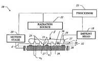
- FIG. 1is a simplified elevation view of a lithographic system in accordance with the present invention
- FIG. 2is a simplified elevation view of a template spaced-apart from the imprinting layer, shown in FIG. 2 , after patterning of the imprinting layer;
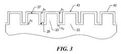
- FIG. 3is a cross-sectional view of the template shown in FIG. 2 with a release layer being disposed thereon.
- FIG. 1depicts a plan view of lithographic system 10 in accordance with one embodiment of the present invention that includes a radiation source 22 coupled to impinge actinic radiation upon a substrate 28 coupled to a motion stage.
- a template 27is coupled to an imprint head 18 to be disposed between substrate 28 and radiation source 22 .
- Motion stage 20 , radiation source 22 and imprint headoperate under control of a processor 21 and are in electrical communication therewith.
- template 27includes a plurality of features defined by a plurality of spaced-apart protrusions 23 having a width w 1 and recesses 25 having a width w 2 .
- Widths w 1 and w 2may be the same or different, depending upon the application.
- a step, defined between an apex surface 27 of protrusions 23 and a nadir surface 29 of recesses 25has a length l, on the order of nanometers, e.g., 30 nanometers.
- the plurality of featuresdefines an original pattern that forms the basis of a desired pattern to be transferred into substrate 28 .
- the desired patternis an inverse of the original pattern and is formed by formation of a recorded pattern on substrate 28 by contacting a flowable region with template 27 .
- imprint head 18is adapted to move along the Z-axis and vary a distance “d” between template 27 and substrate 28 .
- the features on template 27may be imprinted into a conformable region of substrate 28 , discussed more fully below.
- the relative dimensions of the features in the original patterndefine the relative dimensions of the features in the recorded pattern, and therefore, in the desired pattern.
- a conformable regionsuch as an imprinting layer 32 , is disposed on a portion of a surface 34 that presents a substantially smooth, if not planar, profile.
- the conformable regionmay be formed using any known technique to produce conformable material, such as a hot embossing process disclosed in U.S. Pat. No. 5,772,905 to Chou, which is incorporated by reference in its entirety herein, or a laser assisted direct imprinting (LADI) process of the type described by Chou et al. in “Ultrafast and Direct Imprint of Nanostructures in Silicon”, Nature, Col. 447, pp. 835-837, June 4602, which is incorporated by reference in its entirety herein.
- LADIlaser assisted direct imprinting
- the conformable regionconsists of imprinting layer 32 being deposited as a plurality of spaced-apart discrete droplets 30 of an imprinting material.
- Imprinting layer 32is formed from imprinting material that may be selectively polymerized and cross-linked to record the original pattern therein, defining a recorded pattern.
- the recorded pattern 39is produced, in part, by mechanical contact between imprinting layer 32 and template 27 .
- imprint head 18reduces the distance “d” to allow imprinting layer 32 to come into mechanical contact with template 27 , spreading droplets 30 so as to form a contiguous formation of imprinting material over surface 34 .
- distance “d”is reduced to allow recesses 25 to be filled with imprinting material.
- the imprinting materialis provided with the requisite properties to completely fill recesses 25 while covering surface 34 with a contiguous formation of the imprinting material.
- An exemplary imprinting material and imprint lithography processis disclosed in U.S. Pat. No. 6,696,220, entitled TEMPLATE FOR ROOM TEMPERATURE, LOW PRESSURE MICRO-AND NANO-IMPRINT LITHOGRAPHY, as well as, U.S. patent application Ser. Nos. 09/920,341, filed Aug.
- radiation source 22produces actinic radiation that polymerizes and cross-links the imprinting material, forming recorded pattern 39 as cross-linked and polymerized imprinting material.
- the composition of imprinting layertransforms from a flowable imprinting material to a solidified material.
- recorded pattern 39is formed from the cross-linked and polymerized material to provide a side thereof with a shape conforming to a shape of a surface 40 of template 27 .
- recorded pattern 39includes recessions 37 in superimposition with protrusions 23 and projections 35 in superimposition with recesses 25 after the desired, usually minimum distance “d”, has been reached, leaving projections 35 with a thickness t 1 , and recessions 37 with a thickness t 2 .
- Thicknesses “t 1 ” and “t 2 ”may be any thickness desired, dependent upon the application.
- the width u 1 of projections 35is defined by width w 1
- the width u 2 of recessions 37is defined by the width w 2 .
- substrate 28 and imprinting layer 32may be etched to transfer the pattern of imprinting layer 32 into substrate 28 , providing a patterned surface (not shown).
- the material from which imprinting layer 32 is formedmay be varied to define a relative etch rate with respect to substrate 28 , as desired.
- imprinting layer 32may be provided with an etch differential with respect to standard photo-resist material (not shown), e.g., PMMA, selectively disposed thereon.
- the photo-resist material (not shown)may be provided to further pattern imprinting layer 32 , using known techniques. Any etch process may be employed, dependent upon the etch rate desired and the underlying constituents that form substrate 28 and imprinting layer 32 .
- An exemplary radiation source 22may produce ultraviolet radiation; however, any known radiation source may be employed. The selection of radiation employed to initiate the polymerization of the material in imprinting layer 32 is known to one skilled in the art and typically depends on the specific application and materials desired.
- the pattern produced by the present patterning techniquemay be transferred into substrate 28 to provide features having aspect ratios as great as 30:1.
- one embodiment of template 27has recesses 25 defining an aspect ratio in a range of 1:1 to 10:1.
- protrusions 23have a width w 1 in a range of about 10 nm to about 5000 ⁇ m
- recesses 25have a width w 2 in a range of 10 nm to about 5000 ⁇ m.
- template 27may be formed from various conventional materials, including, but not limited to, fused-silica, quartz, silicon, organic polymers, siloxane polymers, borosilicate glass, fluorocarbon polymers, metal, hardened sapphire and the like.
- a desired characteristic of template 27is that the adherence of cross-linked polymer material thereto is minimized.
- a surface of template 27may be treated with a modifying agent, referred to as a release layer 42 .
- release layer 42should adhere well to template 27 without adhering well to recorded pattern 39 , should be relatively transparent to actinic radiation, as well as mechanically sound to minimize premature operational failure. This has been commonly achieved in nanoimprint lithography through the use of, for example, self-assembled monomers (F-SAMS). However, such monolayer coatings are not mechanically robust and can easily be removed through physical contact and microabrasion.
- Diamond-like carbon filmsare coatings that have generally similar properties as polycrystalline diamond coatings, such as low surface friction, low surface energy and high hardness, but unlike diamond coatings, diamond-like carbon coatings are amorphous rather than crystalline.
- Naturally occurring crystalline diamondis formed from a network of sp 3 carbon orbitals, arranged in a local tetrahedral symmetry, maintaining long range crystalline order.
- DLC filmshave a random mixture of tetrahedral sp 3 and hexagonal sp 2 carbon orbitals, with no detectable long range order.
- diamond-like, amorphous carbon filmscan be deposited, depending on the origin of the carbon source and deposition process; hydrogenated and non-hydrogenated DLC films.
- the level of hydrogen and the ratio of sp 3 /sp 2 bondscontrol many of the optical and hardness properties of the material and these in turn can be tailored by choice of starting materials and deposition conditions.
- diamond-like compositionscan be widely modified in their properties by the inclusion of different atomic species into the coating through addition of feed chemicals containing these atoms. The inclusion of such atom can modify film properties such as conductivity, absorbance, strength and surface energy.
- Such atomscan include, without limitation, silicon fluorine, boron and metals.
- diamond-like coating compositionsare available under the tradename DYLYN® from The Bekaert Group, Amherst, N.Y., and as “diamond-like glass” (DLG), examples of which are disclosed in U.S. Pat. No. 6,696,157.
- diamond-like compositionsare characterized by low surface energy material that exhibit excellent release characteristics to cross-linked polymer material 36 .
- surface energies associated with the diamond-like compositionsis in a range of 25 to 40 mN/m (milli-Newtons per meter
- the low surface energies associated with these diamond-like compositionsminimize the adhesion of cross-linked polymer material 36 to template 27 .
- cross-linked polymer material 36 of imprinting layer 32is less likely to tear or shear during separation of template 27 from cross-linked polymer material 36 in imprinting layer 32 .
- Release layer 42is also substantially transparent to actinic radiation, e.g., UV light, such as that emmitted from a mercury or mercury-xenon arc source. Transparency of release layer 42 , as well as template 27 , to actinic radiation is desired in imprint lithography. Without actinic radiation propagating through both release layer 42 and template 27 , solidification and cross-linking of imprinting material would be problematic. To that end, release layer 42 should not have a thicknesses, h 1 and h 2 that would prevent sufficient actinic radiation from propagating therethrough to impinge upon the imprinting material. Thickness h 1 is measured between exposed surface 43 of release layer 42 and apex surface 27 .
- Thickness h 2is measured between exposed surface 43 of release layer 42 and nadir surface 29 .
- release layeris no greater than 500 nm thick.
- the diamond-like amorphous release layeris formed upon the surface 40 of template 27 after being patterned. This has many benefits, such as, low surface energy, diamond-like hardness and ease of application.
- the thickness of the conformal release layeris typically minimized to ensure critical feature dimensions present on template 27 are not unduly modified, and/or lost, but should be thick enough to ensure a pin-hole free coating.
- the differential thickness t 1 -t 2will be substantially unchanged should h 1 and h 2 be substantially equal.
- the dimensions u 1 and u 2may be modified by release layer 42 .
- u 1would be augmented by 2h 3 , where h 3 is a thickness of release layer 42 measured from exposed surface 42 to one of the sidewalls of projections 23 .
- h 3is a thickness of release layer 42 measured from exposed surface 42 to one of the sidewalls of projections 23 .
- u 2would be reduced by the same amount.
- One manner in which to attenuate changes in dimensions of recorded pattern due to the presence of release layer 42is to minimize the thickness h 3 , thereof.
- thickness h 3 , h 2 and h 1are substantially equal. Typically this minimum thickness is of the order of 5 nm.
- the release layermay be deposited onto template 26 employing any known deposition technique that provide the desired conformality, such as chemical vapor deposition (CVD), plasma vapor deposition (PVD), atomic layer deposition (ALD) and the like.
- CVDchemical vapor deposition
- PVDplasma vapor deposition
- ALDatomic layer deposition
- the minimum reduction in u 2is dependent upon the minimum thickness h 3 , which may be difficult to achieve while ensuring a pin-hole free coating of release layer 42 to provide desired release characteristics.
- Another manner in which to apply release layer 42 while minimizing, if not preventing deviations from the dimensions in the desired pattern,is to produce the original pattern with dimensions that differ from the dimensions in the desired pattern.
- the dimensions in the original patternmay be established to compensate for the dimensional variations that the original pattern undergoes as a result of the application of release layer 42 .
- dimensions of the original pattern with release layer 42 disposed thereoncould be established to be equal to the dimensions of the desired pattern.
- dimension w 2 in original patternmay be established as follows: w 1 32 u 1 +2 h 3 (1)
- release layer 42may be doped with conductive materials to facilitate electrical discharge during e-beam lithography and scanning electron microscope inspection. Doping may include metals or other elements. Alternatively, electrically conductive material (not shown) may be applied adjacent to release layer 42 so that release layer 42 is disposed between the electrically conductive material and body 41 .
Landscapes
- Engineering & Computer Science (AREA)
- Mechanical Engineering (AREA)
- Manufacturing & Machinery (AREA)
- Microelectronics & Electronic Packaging (AREA)
- Exposure Of Semiconductors, Excluding Electron Or Ion Beam Exposure (AREA)
- Crystals, And After-Treatments Of Crystals (AREA)
- Carbon And Carbon Compounds (AREA)
Abstract
Description
- The field of the invention relates generally to micro-fabrication of structures. More particularly, the present invention is directed to the production of a template having improved release properties.
- Micro-fabrication involves the fabrication of very small structures, e.g., having features on the order of micro-meters or smaller. One area in which micro-fabrication has had a sizeable impact is in the processing of integrated circuits. As the semiconductor processing industry continues to strive for higher production yields while increasing circuit densities, micro-fabrication becomes increasingly important. Micro-fabrication provides greater process control while allowing reductions in the minimum feature dimension of the structures formed.
- Optical lithography techniques are currently used in micro-fabrication. However, these methods are potentially reaching their limits in resolution. Sub-micron scale lithography has been a crucial process in the microelectronics industry. The use of sub-micron scale lithography allows manufacturers to meet the increased demand for smaller and more densely packed electronic components on chips.
- An exemplary micro-fabrication technique is shown in U.S. Pat. No. 6,334,960 to Willson et al. [hereinafter referred to as Willson]. Willson discloses a method of forming a relief image in a structure. The method includes providing a substrate having a transfer layer. The transfer layer is covered with a polymerizable fluid composition. A template makes mechanical contact with the polymerizable fluid. The template includes a relief structure, and the polymerizable fluid composition fills the relief structure. The polymerizable fluid composition is then subjected to conditions to solidify and polymerize the same, forming a solidified polymeric material on the transfer layer that contains a relief structure complimentary to that of the template. The template is then separated from the solid polymeric material such that a replica of the relief structure in the template is formed in the solidified polymeric material. The transfer layer and the solidified polymeric material are subjected to an environment to selectively etch the transfer layer relative to the solidified polymeric material such that a relief image is formed in the transfer layer. To minimize adhesion between the solidified polymeric material and the template, a release layer is disposed on the template. The release layer functions to provide a low energy surface to enhance template release, thereby minimizing distortions in the pattern due, inter alia, to removal of the template from the solidified polymeric material.
- Thus, a need exists to provide a template with improved release properties.
- The present invention pertains to disposing a conformal diamond-like composition on a patterned template, wherein the diamond-like composition acts as a release layer. The diamond-like composition is deposited so that the release layer is substantially transparent to actinic radiation, e.g., ultraviolet (UV) light, and will also have a desired characteristics, i.e., characterized with a low surface energy that exhibits desirable release properties. Specifically, the low surface energy of the diamond-like composition minimizes the adhesion to the template material compressed between the template and a substrate upon which the imprinting material is disposed. As a result, the material is more likely to adhere to the substrate than to adhere to the template. By reducing the adhesion of the material to the substrate, the quality of the features defined in the material is improved. In addition, the thickness of the diamond-like composition should be established so as to not substantially reduce the critical dimensions of the features of the template. The diamond-like composition may also be doped with a metallic species to allow discharge of electrons. These and other embodiments are described in further detail below.
FIG. 1 is a simplified elevation view of a lithographic system in accordance with the present invention;FIG. 2 is a simplified elevation view of a template spaced-apart from the imprinting layer, shown inFIG. 2 , after patterning of the imprinting layer; andFIG. 3 is a cross-sectional view of the template shown inFIG. 2 with a release layer being disposed thereon.FIG. 1 depicts a plan view oflithographic system 10 in accordance with one embodiment of the present invention that includes aradiation source 22 coupled to impinge actinic radiation upon asubstrate 28 coupled to a motion stage. Atemplate 27 is coupled to animprint head 18 to be disposed betweensubstrate 28 andradiation source 22.Motion stage 20,radiation source 22 and imprint head operate under control of aprocessor 21 and are in electrical communication therewith.- Referring to both
FIGS. 1 and 2 ,template 27 includes a plurality of features defined by a plurality of spaced-apart protrusions 23 having a width w1andrecesses 25 having a width w2. Widths w1and w2, may be the same or different, depending upon the application. A step, defined between anapex surface 27 ofprotrusions 23 and anadir surface 29 ofrecesses 25 has a length l, on the order of nanometers, e.g., 30 nanometers. The plurality of features defines an original pattern that forms the basis of a desired pattern to be transferred intosubstrate 28. Typically the desired pattern is an inverse of the original pattern and is formed by formation of a recorded pattern onsubstrate 28 by contacting a flowable region withtemplate 27. To that end,imprint head 18 is adapted to move along the Z-axis and vary a distance “d” betweentemplate 27 andsubstrate 28. In this manner, the features ontemplate 27 may be imprinted into a conformable region ofsubstrate 28, discussed more fully below. The relative dimensions of the features in the original pattern define the relative dimensions of the features in the recorded pattern, and therefore, in the desired pattern. - A conformable region, such as an
imprinting layer 32, is disposed on a portion of asurface 34 that presents a substantially smooth, if not planar, profile. It should be understood that the conformable region may be formed using any known technique to produce conformable material, such as a hot embossing process disclosed in U.S. Pat. No. 5,772,905 to Chou, which is incorporated by reference in its entirety herein, or a laser assisted direct imprinting (LADI) process of the type described by Chou et al. in “Ultrafast and Direct Imprint of Nanostructures in Silicon”,Nature,Col. 447, pp. 835-837, June 4602, which is incorporated by reference in its entirety herein. In the present embodiment, however, the conformable region consists ofimprinting layer 32 being deposited as a plurality of spaced-apartdiscrete droplets 30 of an imprinting material.Imprinting layer 32 is formed from imprinting material that may be selectively polymerized and cross-linked to record the original pattern therein, defining a recorded pattern. - The recorded
pattern 39 is produced, in part, by mechanical contact betweenimprinting layer 32 andtemplate 27. To that end,imprint head 18 reduces the distance “d” to allowimprinting layer 32 to come into mechanical contact withtemplate 27, spreadingdroplets 30 so as to form a contiguous formation of imprinting material oversurface 34. In one embodiment, distance “d” is reduced to allowrecesses 25 to be filled with imprinting material. - To facilitate filling of
recesses 25, the imprinting material is provided with the requisite properties to completely fillrecesses 25 while coveringsurface 34 with a contiguous formation of the imprinting material. An exemplary imprinting material and imprint lithography process is disclosed in U.S. Pat. No. 6,696,220, entitled TEMPLATE FOR ROOM TEMPERATURE, LOW PRESSURE MICRO-AND NANO-IMPRINT LITHOGRAPHY, as well as, U.S. patent application Ser. Nos. 09/920,341, filed Aug. 1, 2001, entitled METHODS FOR HIGH-PRECISION GAP AND ORIENTATION SENSING BETWEEN A TRANSPARENT TEMPLATE AND SUBSTRATE FOR IMPRINT LITHOGRAPHY, 09/908,455, filed Feb. 12, 2002, entitled METHOD AND SYSTEM OF AUTOMATIC FLUID DISPENSING FOR IMPRINT LITHOGRAPHY PROCESSES, 09/907,512, filed Jul. 16, 2001, entitled HIGH-RESOLUTION OVERLAY ALIGNMENT METHODS AND SYSTEMS FOR IMPRINT LITHOGRAPHY all of which are assigned to assignee of the present invention and incorporated by reference herein. - After a desired distance “d” has been reached,
radiation source 22 produces actinic radiation that polymerizes and cross-links the imprinting material, forming recordedpattern 39 as cross-linked and polymerized imprinting material. As a result, the composition of imprinting layer transforms from a flowable imprinting material to a solidified material. Specifically, recordedpattern 39 is formed from the cross-linked and polymerized material to provide a side thereof with a shape conforming to a shape of asurface 40 oftemplate 27. In this manner, recordedpattern 39 includesrecessions 37 in superimposition withprotrusions 23 andprojections 35 in superimposition withrecesses 25 after the desired, usually minimum distance “d”, has been reached, leavingprojections 35 with a thickness t1, andrecessions 37 with a thickness t2. Thicknesses “t1” and “t2” may be any thickness desired, dependent upon the application. The width u1ofprojections 35 is defined by width w1, and the width u2ofrecessions 37 is defined by the width w2. - After formation of recorded
pattern 39 distance “d” is increased so thattemplate 27 and recordedpattern 39 are spaced-apart. Additional processing may be employed to complete the patterning ofsubstrate 28. For example,substrate 28 andimprinting layer 32 may be etched to transfer the pattern ofimprinting layer 32 intosubstrate 28, providing a patterned surface (not shown). To facilitate etching, the material from whichimprinting layer 32 is formed may be varied to define a relative etch rate with respect tosubstrate 28, as desired. - To that end, imprinting
layer 32 may be provided with an etch differential with respect to standard photo-resist material (not shown), e.g., PMMA, selectively disposed thereon. The photo-resist material (not shown) may be provided to furtherpattern imprinting layer 32, using known techniques. Any etch process may be employed, dependent upon the etch rate desired and the underlying constituents that formsubstrate 28 andimprinting layer 32. Anexemplary radiation source 22 may produce ultraviolet radiation; however, any known radiation source may be employed. The selection of radiation employed to initiate the polymerization of the material inimprinting layer 32 is known to one skilled in the art and typically depends on the specific application and materials desired. - Referring to
FIGS. 1 and 2 , the pattern produced by the present patterning technique may be transferred intosubstrate 28 to provide features having aspect ratios as great as 30:1. To that end, one embodiment oftemplate 27 hasrecesses 25 defining an aspect ratio in a range of 1:1 to 10:1. Specifically,protrusions 23 have a width w1in a range of about 10 nm to about 5000 μm, and recesses25 have a width w2in a range of 10 nm to about 5000 μm. As a result,template 27 may be formed from various conventional materials, including, but not limited to, fused-silica, quartz, silicon, organic polymers, siloxane polymers, borosilicate glass, fluorocarbon polymers, metal, hardened sapphire and the like. - Referring to
FIGS. 2 and 3 , a desired characteristic oftemplate 27 is that the adherence of cross-linked polymer material thereto is minimized. To that end, a surface oftemplate 27 may be treated with a modifying agent, referred to as arelease layer 42. To function satisfactorily, it is desired thatrelease layer 42 should adhere well totemplate 27 without adhering well to recordedpattern 39, should be relatively transparent to actinic radiation, as well as mechanically sound to minimize premature operational failure. This has been commonly achieved in nanoimprint lithography through the use of, for example, self-assembled monomers (F-SAMS). However, such monolayer coatings are not mechanically robust and can easily be removed through physical contact and microabrasion. Materials embodied in the present Invention for use asrelease layer 42 are referred to as diamond-like compositions. Diamond-like carbon films, commonly referred to as “DLC” films, are coatings that have generally similar properties as polycrystalline diamond coatings, such as low surface friction, low surface energy and high hardness, but unlike diamond coatings, diamond-like carbon coatings are amorphous rather than crystalline. Naturally occurring crystalline diamond is formed from a network of sp3carbon orbitals, arranged in a local tetrahedral symmetry, maintaining long range crystalline order. However, DLC films have a random mixture of tetrahedral sp3and hexagonal sp2carbon orbitals, with no detectable long range order. In general, two known categories of diamond-like, amorphous carbon films can be deposited, depending on the origin of the carbon source and deposition process; hydrogenated and non-hydrogenated DLC films. The level of hydrogen and the ratio of sp3/sp2bonds control many of the optical and hardness properties of the material and these in turn can be tailored by choice of starting materials and deposition conditions. In addition to carbon and hydrogen, diamond-like compositions can be widely modified in their properties by the inclusion of different atomic species into the coating through addition of feed chemicals containing these atoms. The inclusion of such atom can modify film properties such as conductivity, absorbance, strength and surface energy. Such atoms can include, without limitation, silicon fluorine, boron and metals. - Examples of diamond like coating compositions are available under the tradename DYLYN® from The Bekaert Group, Amherst, N.Y., and as “diamond-like glass” (DLG), examples of which are disclosed in U.S. Pat. No. 6,696,157. For the purpose of this invention, diamond-like compositions are characterized by low surface energy material that exhibit excellent release characteristics to cross-linked polymer material36. Specifically, surface energies associated with the diamond-like compositions is in a range of 25 to 40 mN/m (milli-Newtons per meter The low surface energies associated with these diamond-like compositions minimize the adhesion of cross-linked polymer material36 to
template 27. As a result, cross-linked polymer material36 ofimprinting layer 32 is less likely to tear or shear during separation oftemplate 27 from cross-linked polymer material36 inimprinting layer 32. Release layer 42 is also substantially transparent to actinic radiation, e.g., UV light, such as that emmitted from a mercury or mercury-xenon arc source. Transparency ofrelease layer 42, as well astemplate 27, to actinic radiation is desired in imprint lithography. Without actinic radiation propagating through bothrelease layer 42 andtemplate 27, solidification and cross-linking of imprinting material would be problematic. To that end,release layer 42 should not have a thicknesses, h1and h2that would prevent sufficient actinic radiation from propagating therethrough to impinge upon the imprinting material. Thickness h1is measured between exposedsurface 43 ofrelease layer 42 andapex surface 27. Thickness h2is measured between exposedsurface 43 ofrelease layer 42 andnadir surface 29. In the present embodiment, release layer is no greater than 500 nm thick. Typically, the diamond-like amorphous release layer is formed upon thesurface 40 oftemplate 27 after being patterned. This has many benefits, such as, low surface energy, diamond-like hardness and ease of application. To that end, the thickness of the conformal release layer is typically minimized to ensure critical feature dimensions present ontemplate 27 are not unduly modified, and/or lost, but should be thick enough to ensure a pin-hole free coating. For example, the differential thickness t1-t2will be substantially unchanged should h1and h2be substantially equal. However, the dimensions u1and u2may be modified byrelease layer 42. Specifically, the dimensions of u1would be augmented by 2h3, where h3is a thickness ofrelease layer 42 measured from exposedsurface 42 to one of the sidewalls ofprojections 23. Conversely, the dimensions of u2would be reduced by the same amount. One manner in which to attenuate changes in dimensions of recorded pattern due to the presence ofrelease layer 42 is to minimize the thickness h3, thereof. Usually thickness h3, h2and h1are substantially equal. Typically this minimum thickness is of the order of 5 nm. The release layer may be deposited onto template26 employing any known deposition technique that provide the desired conformality, such as chemical vapor deposition (CVD), plasma vapor deposition (PVD), atomic layer deposition (ALD) and the like. However, the minimum reduction in u2is dependent upon the minimum thickness h3, which may be difficult to achieve while ensuring a pin-hole free coating ofrelease layer 42 to provide desired release characteristics.- Another manner in which to apply
release layer 42 while minimizing, if not preventing deviations from the dimensions in the desired pattern, is to produce the original pattern with dimensions that differ from the dimensions in the desired pattern. Specifically, the dimensions in the original pattern may be established to compensate for the dimensional variations that the original pattern undergoes as a result of the application ofrelease layer 42. In this manner, dimensions of the original pattern withrelease layer 42 disposed thereon could be established to be equal to the dimensions of the desired pattern. For example, to ensure that the desired pattern has the requisite dimensions, u2and u1, dimension w2in original pattern may be established as follows:
w132 u1+2h3 (1) - Similarly, the dimension w1may be established as follows:
w1=u2−2h3. (2)
Upon application ofrelease layer 42 having a thickness h3, w1and w2would have dimensions equal to the desired dimensions u1and u2, respectively. - In a further embodiment,
release layer 42 may be doped with conductive materials to facilitate electrical discharge during e-beam lithography and scanning electron microscope inspection. Doping may include metals or other elements. Alternatively, electrically conductive material (not shown) may be applied adjacent to releaselayer 42 so thatrelease layer 42 is disposed between the electrically conductive material and body41. - While this invention has been described with references to various illustrative embodiments, the description is not intended to be construed in a limiting sense. Various modifications and combinations of the illustrative embodiments, as well as other embodiments of the invention, will be apparent to persons skilled in the art upon reference to the description. It is, therefore, intended that the appended claims encompass any such modifications or embodiments.
Claims (16)
1. A method of varying release properties of a template having a surface, said method comprising:
disposing a diamond-like composition on said patterned surface, with said diamond-like composition having properties to provide a substantially uniform thickness over said patterned surface while maintaining critical features dimension of features formed in said patterned surface and avoiding pin-holes.
2. The method as recited inclaim 1 wherein disposing further includes disposing said diamond-like composition from a set of diamond-like compositions consisting of including diamond-like carbon (DLC) and diamond-like nano-composites.
3. The method as recited inclaim 2 wherein said nano-composites includes components selected from a set of components consisting essentially of carbon, hydrogen, fluorine, silicon and boron.
4. The method as recited inclaim 1 wherein disposed further includes forming said diamond-like composition to be substantially transmissive to UV radiation.
5. The method as recited inclaim 1 further including doping said diamond-like composition with electrically conductive elements.
6. The method as recited inclaim 1 further including forming said template with a pattern.
7. A method of varying release properties of a template having a patterned surface, said method comprising:
disposing a diamond-like composition on said patterned surface, with said diamond-like composition having properties to provide a substantially uniform thickness over said patterned surface while maintaining critical features dimension of features formed in said patterned surface and being substantially transmissive to a predetermined wavelength of radiation.
8. The method as recited inclaim 7 wherein disposing further includes disposing said diamond-like composition from a set of diamond-like carbon (DLC) and diamond-like nano-composites.
9. The method as recited inclaim 8 wherein said nano-composites includes DYLYN®.
10. The method as recited inclaim 7 wherein said predetermined wavelength includes UV light.
11. The method as recited inclaim 7 further including doping said diamond-like composition with electrically conductive elements.
12. The method as recited inclaim 7 further including forming said template from a fused-silica.
13. A method of varying release properties of a template having a patterned surface, said method comprising:
forming said template from fused-silica;
disposing a diamond-like composition on said patterned surface, with said diamond-like composition having properties to provide a substantially pin-hole free layer over said patterned surface while maintaining critical features dimension of features formed in said patterned surface and being substantially transmissive to UV radiation.
14. The method as recited inclaim 13 wherein disposing further includes disposing said diamond-like composition from a set of diamond-like carbon (DLC) and diamond-like nano-composites.
15. The method as recited inclaim 14 wherein said nano-composites includes components selected from a set of components consisting essentially of carbon, hydrogen, fluorine, silicon and boron.
16. The method as recited inclaim 14 further including doping said diamond-like composition with electrically conductive elements.
Priority Applications (3)
| Application Number | Priority Date | Filing Date | Title |
|---|---|---|---|
| US11/027,473US20060145398A1 (en) | 2004-12-30 | 2004-12-30 | Release layer comprising diamond-like carbon (DLC) or doped DLC with tunable composition for imprint lithography templates and contact masks |
| PCT/US2005/046638WO2006073874A2 (en) | 2004-12-30 | 2005-12-21 | Release layer comprising diamond-like carbon (dlc) or doped dlc with tunable composition |
| TW094146132ATW200641558A (en) | 2004-12-30 | 2005-12-23 | Release layer comprising diamond-like carbon (DLC) or doped DLC with tunable composition for imprint lithography templates and contact masks |
Applications Claiming Priority (1)
| Application Number | Priority Date | Filing Date | Title |
|---|---|---|---|
| US11/027,473US20060145398A1 (en) | 2004-12-30 | 2004-12-30 | Release layer comprising diamond-like carbon (DLC) or doped DLC with tunable composition for imprint lithography templates and contact masks |
Publications (1)
| Publication Number | Publication Date |
|---|---|
| US20060145398A1true US20060145398A1 (en) | 2006-07-06 |
Family
ID=36639509
Family Applications (1)
| Application Number | Title | Priority Date | Filing Date |
|---|---|---|---|
| US11/027,473AbandonedUS20060145398A1 (en) | 2004-12-30 | 2004-12-30 | Release layer comprising diamond-like carbon (DLC) or doped DLC with tunable composition for imprint lithography templates and contact masks |
Country Status (3)
| Country | Link |
|---|---|
| US (1) | US20060145398A1 (en) |
| TW (1) | TW200641558A (en) |
| WO (1) | WO2006073874A2 (en) |
Cited By (25)
| Publication number | Priority date | Publication date | Assignee | Title |
|---|---|---|---|---|
| US20070017631A1 (en)* | 2005-07-22 | 2007-01-25 | Molecular Imprints, Inc. | Method for adhering materials together |
| US7307118B2 (en)* | 2004-11-24 | 2007-12-11 | Molecular Imprints, Inc. | Composition to reduce adhesion between a conformable region and a mold |
| US20080230959A1 (en)* | 2002-12-12 | 2008-09-25 | Board Of Regents, University Of Texas System | Compositions for Dark-Field Polymerization and Method of Using the Same for Imprint Lithography Processes |
| US20090136654A1 (en)* | 2005-10-05 | 2009-05-28 | Molecular Imprints, Inc. | Contact Angle Attenuations on Multiple Surfaces |
| US20090155583A1 (en)* | 2005-07-22 | 2009-06-18 | Molecular Imprints, Inc. | Ultra-thin Polymeric Adhesion Layer |
| US20090197057A1 (en)* | 2008-02-05 | 2009-08-06 | Molecular Imprints, Inc. | Controlling Template Surface Composition in Nano-Imprint Lithography |
| US7670530B2 (en) | 2006-01-20 | 2010-03-02 | Molecular Imprints, Inc. | Patterning substrates employing multiple chucks |
| US7670529B2 (en) | 2005-12-08 | 2010-03-02 | Molecular Imprints, Inc. | Method and system for double-sided patterning of substrates |
| US20100096776A1 (en)* | 2008-10-21 | 2010-04-22 | Molecular Imprints, Inc. | Reduction of Stress During Template Separation |
| US20100102469A1 (en)* | 2008-10-24 | 2010-04-29 | Molecular Imprints, Inc. | Strain and Kinetics Control During Separation Phase of Imprint Process |
| US20100109195A1 (en)* | 2008-11-05 | 2010-05-06 | Molecular Imprints, Inc. | Release agent partition control in imprint lithography |
| US20100112236A1 (en)* | 2008-10-30 | 2010-05-06 | Molecular Imprints, Inc. | Facilitating Adhesion Between Substrate and Patterned Layer |
| US20100110409A1 (en)* | 2008-10-30 | 2010-05-06 | Molecular Imprints, Inc. | Separation in an Imprint Lithography Process |
| US7759407B2 (en) | 2005-07-22 | 2010-07-20 | Molecular Imprints, Inc. | Composition for adhering materials together |
| US20100276290A1 (en)* | 2009-04-30 | 2010-11-04 | Masamitsu Itoh | Patterning method, patterning apparatus, and method for manufacturing semiconductor device |
| US7837921B2 (en) | 2004-01-23 | 2010-11-23 | Molecular Imprints, Inc. | Method of providing desirable wetting and release characteristics between a mold and a polymerizable composition |
| US7939131B2 (en) | 2004-08-16 | 2011-05-10 | Molecular Imprints, Inc. | Method to provide a layer with uniform etch characteristics |
| US20110146568A1 (en)* | 2007-12-21 | 2011-06-23 | Asm International N.V. | Modification of nanoimprint lithography templates by atomic layer deposition |
| US20110165412A1 (en)* | 2009-11-24 | 2011-07-07 | Molecular Imprints, Inc. | Adhesion layers in nanoimprint lithograhy |
| US7981481B2 (en) | 2004-09-23 | 2011-07-19 | Molecular Imprints, Inc. | Method for controlling distribution of fluid components on a body |
| US20110215503A1 (en)* | 2004-11-24 | 2011-09-08 | Molecular Imprints, Inc. | Reducing Adhesion between a Conformable Region and a Mold |
| US20120319314A1 (en)* | 2011-06-15 | 2012-12-20 | Hon Hai Precision Industry Co., Ltd. | Method for fabricating light guide plate |
| US8808808B2 (en) | 2005-07-22 | 2014-08-19 | Molecular Imprints, Inc. | Method for imprint lithography utilizing an adhesion primer layer |
| US20180216593A1 (en)* | 2017-02-01 | 2018-08-02 | GM Global Technology Operations LLC | Diamond like carbon (dlc) coating for ethanol-blended fuel injector applications |
| CN108501361A (en)* | 2017-02-28 | 2018-09-07 | 香港理工大学 | Rapid forming device and rapid forming method for nano-micro structural part |
Families Citing this family (1)
| Publication number | Priority date | Publication date | Assignee | Title |
|---|---|---|---|---|
| JP5295102B2 (en)* | 2007-04-20 | 2013-09-18 | ナノテック株式会社 | Conductive protective film and manufacturing method thereof |
Citations (94)
| Publication number | Priority date | Publication date | Assignee | Title |
|---|---|---|---|---|
| US3783520A (en)* | 1970-09-28 | 1974-01-08 | Bell Telephone Labor Inc | High accuracy alignment procedure utilizing moire patterns |
| US4070116A (en)* | 1975-06-23 | 1978-01-24 | International Business Machines Corporation | Gap measuring device for defining the distance between two or more surfaces |
| US4201800A (en)* | 1978-04-28 | 1980-05-06 | International Business Machines Corp. | Hardened photoresist master image mask process |
| US4426247A (en)* | 1982-04-12 | 1984-01-17 | Nippon Telegraph & Telephone Public Corporation | Method for forming micropattern |
| US4507331A (en)* | 1983-12-12 | 1985-03-26 | International Business Machines Corporation | Dry process for forming positive tone micro patterns |
| US4512846A (en)* | 1982-01-26 | 1985-04-23 | The United States Of America As Represented By The Administrator Of The National Aeronautics And Space Administration | Method for growth of crystals by pressure reduction of supercritical or subcritical solution |
| US4657845A (en)* | 1986-01-14 | 1987-04-14 | International Business Machines Corporation | Positive tone oxygen plasma developable photoresist |
| US4724222A (en)* | 1986-04-28 | 1988-02-09 | American Telephone And Telegraph Company, At&T Bell Laboratories | Wafer chuck comprising a curved reference surface |
| US4731155A (en)* | 1987-04-15 | 1988-03-15 | General Electric Company | Process for forming a lithographic mask |
| US4737425A (en)* | 1986-06-10 | 1988-04-12 | International Business Machines Corporation | Patterned resist and process |
| US4826943A (en)* | 1986-07-25 | 1989-05-02 | Oki Electric Industry Co., Ltd. | Negative resist material |
| US4891303A (en)* | 1988-05-26 | 1990-01-02 | Texas Instruments Incorporated | Trilayer microlithographic process using a silicon-based resist as the middle layer |
| US4908298A (en)* | 1985-03-19 | 1990-03-13 | International Business Machines Corporation | Method of creating patterned multilayer films for use in production of semiconductor circuits and systems |
| US4919748A (en)* | 1989-06-30 | 1990-04-24 | At&T Bell Laboratories | Method for tapered etching |
| US4921778A (en)* | 1988-07-29 | 1990-05-01 | Shipley Company Inc. | Photoresist pattern fabrication employing chemically amplified metalized material |
| US4929083A (en)* | 1986-06-19 | 1990-05-29 | Xerox Corporation | Focus and overlay characterization and optimization for photolithographic exposure |
| US4999280A (en)* | 1989-03-17 | 1991-03-12 | International Business Machines Corporation | Spray silylation of photoresist images |
| US5110514A (en)* | 1989-05-01 | 1992-05-05 | Soane Technologies, Inc. | Controlled casting of a shrinkable material |
| US5179863A (en)* | 1990-03-05 | 1993-01-19 | Kabushiki Kaisha Toshiba | Method and apparatus for setting the gap distance between a mask and a wafer at a predetermined distance |
| US5198326A (en)* | 1990-05-24 | 1993-03-30 | Matsushita Electric Industrial Co., Ltd. | Process for forming fine pattern |
| US5204739A (en)* | 1992-02-07 | 1993-04-20 | Karl Suss America, Inc. | Proximity mask alignment using a stored video image |
| US5206983A (en)* | 1991-06-24 | 1993-05-04 | Wisconsin Alumni Research Foundation | Method of manufacturing micromechanical devices |
| US5212147A (en)* | 1991-05-15 | 1993-05-18 | Hewlett-Packard Company | Method of forming a patterned in-situ high Tc superconductive film |
| US5277749A (en)* | 1991-10-17 | 1994-01-11 | International Business Machines Corporation | Methods and apparatus for relieving stress and resisting stencil delamination when performing lift-off processes that utilize high stress metals and/or multiple evaporation steps |
| US5314772A (en)* | 1990-10-09 | 1994-05-24 | Arizona Board Of Regents | High resolution, multi-layer resist for microlithography and method therefor |
| US5392123A (en)* | 1991-09-06 | 1995-02-21 | Eastman Kodak Company | Optical monitor for measuring a gap between two rollers |
| US5480047A (en)* | 1993-06-04 | 1996-01-02 | Sharp Kabushiki Kaisha | Method for forming a fine resist pattern |
| US5515167A (en)* | 1994-09-13 | 1996-05-07 | Hughes Aircraft Company | Transparent optical chuck incorporating optical monitoring |
| US5594042A (en)* | 1993-05-18 | 1997-01-14 | Dow Corning Corporation | Radiation curable compositions containing vinyl ether functional polyorganosiloxanes |
| US5601641A (en)* | 1992-07-21 | 1997-02-11 | Tse Industries, Inc. | Mold release composition with polybutadiene and method of coating a mold core |
| US5629095A (en)* | 1993-05-18 | 1997-05-13 | Dow Corning Corporation | Radiation curable compositions containing vinyl ether functional polysiloxanes and methods for the preparation |
| US5633505A (en)* | 1995-09-29 | 1997-05-27 | Taiwan Semiconductor Manufacturing Company, Ltd. | Semiconductor wafer incorporating marks for inspecting first layer overlay shift in global alignment process |
| US5723176A (en)* | 1994-03-02 | 1998-03-03 | Telecommunications Research Laboratories | Method and apparatus for making optical components by direct dispensing of curable liquid |
| US5724145A (en)* | 1995-07-17 | 1998-03-03 | Seiko Epson Corporation | Optical film thickness measurement method, film formation method, and semiconductor laser fabrication method |
| US5736424A (en)* | 1987-02-27 | 1998-04-07 | Lucent Technologies Inc. | Device fabrication involving planarization |
| US5743998A (en)* | 1995-04-19 | 1998-04-28 | Park Scientific Instruments | Process for transferring microminiature patterns using spin-on glass resist media |
| US5747102A (en)* | 1995-11-16 | 1998-05-05 | Nordson Corporation | Method and apparatus for dispensing small amounts of liquid material |
| US5855686A (en)* | 1994-05-24 | 1999-01-05 | Depositech, Inc. | Method and apparatus for vacuum deposition of highly ionized media in an electromagnetic controlled environment |
| US5877036A (en)* | 1996-02-29 | 1999-03-02 | Nec Corporation | Overlay measuring method using correlation function |
| US5877861A (en)* | 1997-11-14 | 1999-03-02 | International Business Machines Corporation | Method for overlay control system |
| US5895263A (en)* | 1996-12-19 | 1999-04-20 | International Business Machines Corporation | Process for manufacture of integrated circuit device |
| US5900160A (en)* | 1993-10-04 | 1999-05-04 | President And Fellows Of Harvard College | Methods of etching articles via microcontact printing |
| US5907782A (en)* | 1998-08-15 | 1999-05-25 | Acer Semiconductor Manufacturing Inc. | Method of forming a multiple fin-pillar capacitor for a high density dram cell |
| US6033977A (en)* | 1997-06-30 | 2000-03-07 | Siemens Aktiengesellschaft | Dual damascene structure |
| US6038280A (en)* | 1997-03-13 | 2000-03-14 | Helmut Fischer Gmbh & Co. Institut Fur Electronik Und Messtechnik | Method and apparatus for measuring the thicknesses of thin layers by means of x-ray fluorescence |
| US6039897A (en)* | 1996-08-28 | 2000-03-21 | University Of Washington | Multiple patterned structures on a single substrate fabricated by elastomeric micro-molding techniques |
| US6046056A (en)* | 1996-06-28 | 2000-04-04 | Caliper Technologies Corporation | High throughput screening assay systems in microscale fluidic devices |
| US6051345A (en)* | 1998-04-27 | 2000-04-18 | United Microelectronics Corp. | Method of producing phase shifting mask |
| US6168845B1 (en)* | 1999-01-19 | 2001-01-02 | International Business Machines Corporation | Patterned magnetic media and method of making the same using selective oxidation |
| US6180239B1 (en)* | 1993-10-04 | 2001-01-30 | President And Fellows Of Harvard College | Microcontact printing on surfaces and derivative articles |
| US6188150B1 (en)* | 1999-06-16 | 2001-02-13 | Euv, Llc | Light weight high-stiffness stage platen |
| US6190929B1 (en)* | 1999-07-23 | 2001-02-20 | Micron Technology, Inc. | Methods of forming semiconductor devices and methods of forming field emission displays |
| US6204922B1 (en)* | 1998-12-11 | 2001-03-20 | Filmetrics, Inc. | Rapid and accurate thin film measurement of individual layers in a multi-layered or patterned sample |
| US6334960B1 (en)* | 1999-03-11 | 2002-01-01 | Board Of Regents, The University Of Texas System | Step and flash imprint lithography |
| US20020042027A1 (en)* | 1998-10-09 | 2002-04-11 | Chou Stephen Y. | Microscale patterning and articles formed thereby |
| US6383928B1 (en)* | 1999-09-02 | 2002-05-07 | Texas Instruments Incorporated | Post copper CMP clean |
| US6387787B1 (en)* | 2001-03-02 | 2002-05-14 | Motorola, Inc. | Lithographic template and method of formation and use |
| US6387783B1 (en)* | 1999-04-26 | 2002-05-14 | International Business Machines Corporation | Methods of T-gate fabrication using a hybrid resist |
| US6388253B1 (en)* | 1999-06-29 | 2002-05-14 | Applied Materials, Inc. | Integrated critical dimension control for semiconductor device manufacturing |
| US6391217B2 (en)* | 1999-12-23 | 2002-05-21 | University Of Massachusetts | Methods and apparatus for forming submicron patterns on films |
| US6391798B1 (en)* | 1987-02-27 | 2002-05-21 | Agere Systems Guardian Corp. | Process for planarization a semiconductor substrate |
| US6514672B2 (en)* | 1999-06-17 | 2003-02-04 | Taiwan Semiconductor Manufacturing Company | Dry development process for a bi-layer resist system |
| US6517995B1 (en)* | 1999-09-14 | 2003-02-11 | Massachusetts Institute Of Technology | Fabrication of finely featured devices by liquid embossing |
| US6518189B1 (en)* | 1995-11-15 | 2003-02-11 | Regents Of The University Of Minnesota | Method and apparatus for high density nanostructures |
| US6517977B2 (en)* | 2001-03-28 | 2003-02-11 | Motorola, Inc. | Lithographic template and method of formation and use |
| US20030034329A1 (en)* | 1998-06-30 | 2003-02-20 | Chou Stephen Y. | Lithographic method for molding pattern with nanoscale depth |
| US6534418B1 (en)* | 2001-04-30 | 2003-03-18 | Advanced Micro Devices, Inc. | Use of silicon containing imaging layer to define sub-resolution gate structures |
| US6541360B1 (en)* | 2001-04-30 | 2003-04-01 | Advanced Micro Devices, Inc. | Bi-layer trim etch process to form integrated circuit gate structures |
| US20030081193A1 (en)* | 2001-06-01 | 2003-05-01 | White Donald L. | Holder, system, and process for improving overlay in lithography |
| US20030080472A1 (en)* | 2001-10-29 | 2003-05-01 | Chou Stephen Y. | Lithographic method with bonded release layer for molding small patterns |
| US6561706B2 (en)* | 2001-06-28 | 2003-05-13 | Advanced Micro Devices, Inc. | Critical dimension monitoring from latent image |
| US6565928B2 (en)* | 1999-03-08 | 2003-05-20 | Tokyo Electron Limited | Film forming method and film forming apparatus |
| US6677252B2 (en)* | 1998-10-22 | 2004-01-13 | Micron Technology, Inc. | Methods for planarization of non-planar surfaces in device fabrication |
| US20040008334A1 (en)* | 2002-07-11 | 2004-01-15 | Sreenivasan Sidlgata V. | Step and repeat imprint lithography systems |
| US20040009673A1 (en)* | 2002-07-11 | 2004-01-15 | Sreenivasan Sidlgata V. | Method and system for imprint lithography using an electric field |
| US20040007799A1 (en)* | 2002-07-11 | 2004-01-15 | Choi Byung Jin | Formation of discontinuous films during an imprint lithography process |
| US20040022888A1 (en)* | 2002-08-01 | 2004-02-05 | Sreenivasan Sidlgata V. | Alignment systems for imprint lithography |
| US20040021866A1 (en)* | 2002-08-01 | 2004-02-05 | Watts Michael P.C. | Scatterometry alignment for imprint lithography |
| US20040021254A1 (en)* | 2002-08-01 | 2004-02-05 | Sreenivasan Sidlgata V. | Alignment methods for imprint lithography |
| US20040029041A1 (en)* | 2002-02-27 | 2004-02-12 | Brewer Science, Inc. | Novel planarization method for multi-layer lithography processing |
| US6696220B2 (en)* | 2000-10-12 | 2004-02-24 | Board Of Regents, The University Of Texas System | Template for room temperature, low pressure micro-and nano-imprint lithography |
| US20040036201A1 (en)* | 2000-07-18 | 2004-02-26 | Princeton University | Methods and apparatus of field-induced pressure imprint lithography |
| US6703190B2 (en)* | 1999-12-07 | 2004-03-09 | Infineon Technologies Ag | Method for producing resist structures |
| US20040046288A1 (en)* | 2000-07-18 | 2004-03-11 | Chou Stephen Y. | Laset assisted direct imprint lithography |
| US20040046271A1 (en)* | 2002-09-05 | 2004-03-11 | Watts Michael P.C. | Functional patterning material for imprint lithography processes |
| US6716767B2 (en)* | 2001-10-31 | 2004-04-06 | Brewer Science, Inc. | Contact planarization materials that generate no volatile byproducts or residue during curing |
| US6716754B2 (en)* | 2002-03-12 | 2004-04-06 | Micron Technology, Inc. | Methods of forming patterns and molds for semiconductor constructions |
| US20040065252A1 (en)* | 2002-10-04 | 2004-04-08 | Sreenivasan Sidlgata V. | Method of forming a layer on a substrate to facilitate fabrication of metrology standards |
| US6730256B1 (en)* | 2000-08-04 | 2004-05-04 | Massachusetts Institute Of Technology | Stereolithographic patterning with interlayer surface modifications |
| US20040090611A1 (en)* | 2002-11-13 | 2004-05-13 | Molecular Imprints, Inc. | Chucking system for modulating shapes of substrates |
| US6737202B2 (en)* | 2002-02-22 | 2004-05-18 | Motorola, Inc. | Method of fabricating a tiered structure using a multi-layered resist stack and use |
| US20050064344A1 (en)* | 2003-09-18 | 2005-03-24 | University Of Texas System Board Of Regents | Imprint lithography templates having alignment marks |
| US20050067379A1 (en)* | 2003-09-25 | 2005-03-31 | Molecular Imprints, Inc. | Imprint lithography template having opaque alignment marks |
| US20050098534A1 (en)* | 2003-11-12 | 2005-05-12 | Molecular Imprints, Inc. | Formation of conductive templates employing indium tin oxide |
- 2004
- 2004-12-30USUS11/027,473patent/US20060145398A1/ennot_activeAbandoned
- 2005
- 2005-12-21WOPCT/US2005/046638patent/WO2006073874A2/enactiveApplication Filing
- 2005-12-23TWTW094146132Apatent/TW200641558A/enunknown
Patent Citations (99)
| Publication number | Priority date | Publication date | Assignee | Title |
|---|---|---|---|---|
| US3783520A (en)* | 1970-09-28 | 1974-01-08 | Bell Telephone Labor Inc | High accuracy alignment procedure utilizing moire patterns |
| US4070116A (en)* | 1975-06-23 | 1978-01-24 | International Business Machines Corporation | Gap measuring device for defining the distance between two or more surfaces |
| US4201800A (en)* | 1978-04-28 | 1980-05-06 | International Business Machines Corp. | Hardened photoresist master image mask process |
| US4512846A (en)* | 1982-01-26 | 1985-04-23 | The United States Of America As Represented By The Administrator Of The National Aeronautics And Space Administration | Method for growth of crystals by pressure reduction of supercritical or subcritical solution |
| US4426247A (en)* | 1982-04-12 | 1984-01-17 | Nippon Telegraph & Telephone Public Corporation | Method for forming micropattern |
| US4507331A (en)* | 1983-12-12 | 1985-03-26 | International Business Machines Corporation | Dry process for forming positive tone micro patterns |
| US4908298A (en)* | 1985-03-19 | 1990-03-13 | International Business Machines Corporation | Method of creating patterned multilayer films for use in production of semiconductor circuits and systems |
| US4657845A (en)* | 1986-01-14 | 1987-04-14 | International Business Machines Corporation | Positive tone oxygen plasma developable photoresist |
| US4724222A (en)* | 1986-04-28 | 1988-02-09 | American Telephone And Telegraph Company, At&T Bell Laboratories | Wafer chuck comprising a curved reference surface |
| US4737425A (en)* | 1986-06-10 | 1988-04-12 | International Business Machines Corporation | Patterned resist and process |
| US4929083A (en)* | 1986-06-19 | 1990-05-29 | Xerox Corporation | Focus and overlay characterization and optimization for photolithographic exposure |
| US4826943A (en)* | 1986-07-25 | 1989-05-02 | Oki Electric Industry Co., Ltd. | Negative resist material |
| US6391798B1 (en)* | 1987-02-27 | 2002-05-21 | Agere Systems Guardian Corp. | Process for planarization a semiconductor substrate |
| US5736424A (en)* | 1987-02-27 | 1998-04-07 | Lucent Technologies Inc. | Device fabrication involving planarization |
| US4731155A (en)* | 1987-04-15 | 1988-03-15 | General Electric Company | Process for forming a lithographic mask |
| US4891303A (en)* | 1988-05-26 | 1990-01-02 | Texas Instruments Incorporated | Trilayer microlithographic process using a silicon-based resist as the middle layer |
| US4921778A (en)* | 1988-07-29 | 1990-05-01 | Shipley Company Inc. | Photoresist pattern fabrication employing chemically amplified metalized material |
| US4999280A (en)* | 1989-03-17 | 1991-03-12 | International Business Machines Corporation | Spray silylation of photoresist images |
| US5110514A (en)* | 1989-05-01 | 1992-05-05 | Soane Technologies, Inc. | Controlled casting of a shrinkable material |
| US4919748A (en)* | 1989-06-30 | 1990-04-24 | At&T Bell Laboratories | Method for tapered etching |
| US5179863A (en)* | 1990-03-05 | 1993-01-19 | Kabushiki Kaisha Toshiba | Method and apparatus for setting the gap distance between a mask and a wafer at a predetermined distance |
| US5198326A (en)* | 1990-05-24 | 1993-03-30 | Matsushita Electric Industrial Co., Ltd. | Process for forming fine pattern |
| US5314772A (en)* | 1990-10-09 | 1994-05-24 | Arizona Board Of Regents | High resolution, multi-layer resist for microlithography and method therefor |
| US5212147A (en)* | 1991-05-15 | 1993-05-18 | Hewlett-Packard Company | Method of forming a patterned in-situ high Tc superconductive film |
| US5206983A (en)* | 1991-06-24 | 1993-05-04 | Wisconsin Alumni Research Foundation | Method of manufacturing micromechanical devices |
| US5392123A (en)* | 1991-09-06 | 1995-02-21 | Eastman Kodak Company | Optical monitor for measuring a gap between two rollers |
| US5277749A (en)* | 1991-10-17 | 1994-01-11 | International Business Machines Corporation | Methods and apparatus for relieving stress and resisting stencil delamination when performing lift-off processes that utilize high stress metals and/or multiple evaporation steps |
| US5204739A (en)* | 1992-02-07 | 1993-04-20 | Karl Suss America, Inc. | Proximity mask alignment using a stored video image |
| US5601641A (en)* | 1992-07-21 | 1997-02-11 | Tse Industries, Inc. | Mold release composition with polybutadiene and method of coating a mold core |
| US5594042A (en)* | 1993-05-18 | 1997-01-14 | Dow Corning Corporation | Radiation curable compositions containing vinyl ether functional polyorganosiloxanes |
| US5629095A (en)* | 1993-05-18 | 1997-05-13 | Dow Corning Corporation | Radiation curable compositions containing vinyl ether functional polysiloxanes and methods for the preparation |
| US5861467A (en)* | 1993-05-18 | 1999-01-19 | Dow Corning Corporation | Radiation curable siloxane compositions containing vinyl ether functionality and methods for their preparation |
| US5480047A (en)* | 1993-06-04 | 1996-01-02 | Sharp Kabushiki Kaisha | Method for forming a fine resist pattern |
| US6180239B1 (en)* | 1993-10-04 | 2001-01-30 | President And Fellows Of Harvard College | Microcontact printing on surfaces and derivative articles |
| US5900160A (en)* | 1993-10-04 | 1999-05-04 | President And Fellows Of Harvard College | Methods of etching articles via microcontact printing |
| US5723176A (en)* | 1994-03-02 | 1998-03-03 | Telecommunications Research Laboratories | Method and apparatus for making optical components by direct dispensing of curable liquid |
| US5855686A (en)* | 1994-05-24 | 1999-01-05 | Depositech, Inc. | Method and apparatus for vacuum deposition of highly ionized media in an electromagnetic controlled environment |
| US6035805A (en)* | 1994-05-24 | 2000-03-14 | Depositech, Inc. | Method and apparatus for vacuum deposition of highly ionized media in an electromagnetic controlled environment |
| US5515167A (en)* | 1994-09-13 | 1996-05-07 | Hughes Aircraft Company | Transparent optical chuck incorporating optical monitoring |
| US5743998A (en)* | 1995-04-19 | 1998-04-28 | Park Scientific Instruments | Process for transferring microminiature patterns using spin-on glass resist media |
| US5724145A (en)* | 1995-07-17 | 1998-03-03 | Seiko Epson Corporation | Optical film thickness measurement method, film formation method, and semiconductor laser fabrication method |
| US5633505A (en)* | 1995-09-29 | 1997-05-27 | Taiwan Semiconductor Manufacturing Company, Ltd. | Semiconductor wafer incorporating marks for inspecting first layer overlay shift in global alignment process |
| US6518189B1 (en)* | 1995-11-15 | 2003-02-11 | Regents Of The University Of Minnesota | Method and apparatus for high density nanostructures |
| US5747102A (en)* | 1995-11-16 | 1998-05-05 | Nordson Corporation | Method and apparatus for dispensing small amounts of liquid material |
| US5877036A (en)* | 1996-02-29 | 1999-03-02 | Nec Corporation | Overlay measuring method using correlation function |
| US6046056A (en)* | 1996-06-28 | 2000-04-04 | Caliper Technologies Corporation | High throughput screening assay systems in microscale fluidic devices |
| US6039897A (en)* | 1996-08-28 | 2000-03-21 | University Of Washington | Multiple patterned structures on a single substrate fabricated by elastomeric micro-molding techniques |
| US5895263A (en)* | 1996-12-19 | 1999-04-20 | International Business Machines Corporation | Process for manufacture of integrated circuit device |
| US6038280A (en)* | 1997-03-13 | 2000-03-14 | Helmut Fischer Gmbh & Co. Institut Fur Electronik Und Messtechnik | Method and apparatus for measuring the thicknesses of thin layers by means of x-ray fluorescence |
| US6033977A (en)* | 1997-06-30 | 2000-03-07 | Siemens Aktiengesellschaft | Dual damascene structure |
| US5877861A (en)* | 1997-11-14 | 1999-03-02 | International Business Machines Corporation | Method for overlay control system |
| US6051345A (en)* | 1998-04-27 | 2000-04-18 | United Microelectronics Corp. | Method of producing phase shifting mask |
| US20030034329A1 (en)* | 1998-06-30 | 2003-02-20 | Chou Stephen Y. | Lithographic method for molding pattern with nanoscale depth |
| US5907782A (en)* | 1998-08-15 | 1999-05-25 | Acer Semiconductor Manufacturing Inc. | Method of forming a multiple fin-pillar capacitor for a high density dram cell |
| US20020042027A1 (en)* | 1998-10-09 | 2002-04-11 | Chou Stephen Y. | Microscale patterning and articles formed thereby |
| US6713238B1 (en)* | 1998-10-09 | 2004-03-30 | Stephen Y. Chou | Microscale patterning and articles formed thereby |
| US6677252B2 (en)* | 1998-10-22 | 2004-01-13 | Micron Technology, Inc. | Methods for planarization of non-planar surfaces in device fabrication |
| US6204922B1 (en)* | 1998-12-11 | 2001-03-20 | Filmetrics, Inc. | Rapid and accurate thin film measurement of individual layers in a multi-layered or patterned sample |
| US6168845B1 (en)* | 1999-01-19 | 2001-01-02 | International Business Machines Corporation | Patterned magnetic media and method of making the same using selective oxidation |
| US6565928B2 (en)* | 1999-03-08 | 2003-05-20 | Tokyo Electron Limited | Film forming method and film forming apparatus |
| US6334960B1 (en)* | 1999-03-11 | 2002-01-01 | Board Of Regents, The University Of Texas System | Step and flash imprint lithography |
| US6719915B2 (en)* | 1999-03-11 | 2004-04-13 | Board Of Regents, The University Of Texas System | Step and flash imprint lithography |
| US6387783B1 (en)* | 1999-04-26 | 2002-05-14 | International Business Machines Corporation | Methods of T-gate fabrication using a hybrid resist |
| US6188150B1 (en)* | 1999-06-16 | 2001-02-13 | Euv, Llc | Light weight high-stiffness stage platen |
| US6514672B2 (en)* | 1999-06-17 | 2003-02-04 | Taiwan Semiconductor Manufacturing Company | Dry development process for a bi-layer resist system |
| US6388253B1 (en)* | 1999-06-29 | 2002-05-14 | Applied Materials, Inc. | Integrated critical dimension control for semiconductor device manufacturing |
| US6190929B1 (en)* | 1999-07-23 | 2001-02-20 | Micron Technology, Inc. | Methods of forming semiconductor devices and methods of forming field emission displays |
| US6383928B1 (en)* | 1999-09-02 | 2002-05-07 | Texas Instruments Incorporated | Post copper CMP clean |
| US6517995B1 (en)* | 1999-09-14 | 2003-02-11 | Massachusetts Institute Of Technology | Fabrication of finely featured devices by liquid embossing |
| US6703190B2 (en)* | 1999-12-07 | 2004-03-09 | Infineon Technologies Ag | Method for producing resist structures |
| US6391217B2 (en)* | 1999-12-23 | 2002-05-21 | University Of Massachusetts | Methods and apparatus for forming submicron patterns on films |
| US20040046288A1 (en)* | 2000-07-18 | 2004-03-11 | Chou Stephen Y. | Laset assisted direct imprint lithography |
| US20040036201A1 (en)* | 2000-07-18 | 2004-02-26 | Princeton University | Methods and apparatus of field-induced pressure imprint lithography |
| US6730256B1 (en)* | 2000-08-04 | 2004-05-04 | Massachusetts Institute Of Technology | Stereolithographic patterning with interlayer surface modifications |
| US6696220B2 (en)* | 2000-10-12 | 2004-02-24 | Board Of Regents, The University Of Texas System | Template for room temperature, low pressure micro-and nano-imprint lithography |
| US6387787B1 (en)* | 2001-03-02 | 2002-05-14 | Motorola, Inc. | Lithographic template and method of formation and use |
| US6517977B2 (en)* | 2001-03-28 | 2003-02-11 | Motorola, Inc. | Lithographic template and method of formation and use |
| US6534418B1 (en)* | 2001-04-30 | 2003-03-18 | Advanced Micro Devices, Inc. | Use of silicon containing imaging layer to define sub-resolution gate structures |
| US6541360B1 (en)* | 2001-04-30 | 2003-04-01 | Advanced Micro Devices, Inc. | Bi-layer trim etch process to form integrated circuit gate structures |
| US20030081193A1 (en)* | 2001-06-01 | 2003-05-01 | White Donald L. | Holder, system, and process for improving overlay in lithography |
| US6561706B2 (en)* | 2001-06-28 | 2003-05-13 | Advanced Micro Devices, Inc. | Critical dimension monitoring from latent image |
| US20030080471A1 (en)* | 2001-10-29 | 2003-05-01 | Chou Stephen Y. | Lithographic method for molding pattern with nanoscale features |
| US20030080472A1 (en)* | 2001-10-29 | 2003-05-01 | Chou Stephen Y. | Lithographic method with bonded release layer for molding small patterns |
| US6716767B2 (en)* | 2001-10-31 | 2004-04-06 | Brewer Science, Inc. | Contact planarization materials that generate no volatile byproducts or residue during curing |
| US6737202B2 (en)* | 2002-02-22 | 2004-05-18 | Motorola, Inc. | Method of fabricating a tiered structure using a multi-layered resist stack and use |
| US20040029041A1 (en)* | 2002-02-27 | 2004-02-12 | Brewer Science, Inc. | Novel planarization method for multi-layer lithography processing |
| US6716754B2 (en)* | 2002-03-12 | 2004-04-06 | Micron Technology, Inc. | Methods of forming patterns and molds for semiconductor constructions |
| US20040007799A1 (en)* | 2002-07-11 | 2004-01-15 | Choi Byung Jin | Formation of discontinuous films during an imprint lithography process |
| US20040009673A1 (en)* | 2002-07-11 | 2004-01-15 | Sreenivasan Sidlgata V. | Method and system for imprint lithography using an electric field |
| US20040008334A1 (en)* | 2002-07-11 | 2004-01-15 | Sreenivasan Sidlgata V. | Step and repeat imprint lithography systems |
| US20040021254A1 (en)* | 2002-08-01 | 2004-02-05 | Sreenivasan Sidlgata V. | Alignment methods for imprint lithography |
| US20040021866A1 (en)* | 2002-08-01 | 2004-02-05 | Watts Michael P.C. | Scatterometry alignment for imprint lithography |
| US20040022888A1 (en)* | 2002-08-01 | 2004-02-05 | Sreenivasan Sidlgata V. | Alignment systems for imprint lithography |
| US20040046271A1 (en)* | 2002-09-05 | 2004-03-11 | Watts Michael P.C. | Functional patterning material for imprint lithography processes |
| US20040065252A1 (en)* | 2002-10-04 | 2004-04-08 | Sreenivasan Sidlgata V. | Method of forming a layer on a substrate to facilitate fabrication of metrology standards |
| US20040090611A1 (en)* | 2002-11-13 | 2004-05-13 | Molecular Imprints, Inc. | Chucking system for modulating shapes of substrates |
| US20050064344A1 (en)* | 2003-09-18 | 2005-03-24 | University Of Texas System Board Of Regents | Imprint lithography templates having alignment marks |
| US20050067379A1 (en)* | 2003-09-25 | 2005-03-31 | Molecular Imprints, Inc. | Imprint lithography template having opaque alignment marks |
| US20050098534A1 (en)* | 2003-11-12 | 2005-05-12 | Molecular Imprints, Inc. | Formation of conductive templates employing indium tin oxide |
Cited By (44)
| Publication number | Priority date | Publication date | Assignee | Title |
|---|---|---|---|---|
| US20080230959A1 (en)* | 2002-12-12 | 2008-09-25 | Board Of Regents, University Of Texas System | Compositions for Dark-Field Polymerization and Method of Using the Same for Imprint Lithography Processes |
| US7906060B2 (en) | 2002-12-12 | 2011-03-15 | Board Of Regents, The University Of Texas System | Compositions for dark-field polymerization and method of using the same for imprint lithography processes |
| US20090272875A1 (en)* | 2003-06-17 | 2009-11-05 | Molecular Imprints, Inc. | Composition to Reduce Adhesion Between a Conformable Region and a Mold |
| US8152511B2 (en) | 2003-06-17 | 2012-04-10 | Molecular Imprints, Inc. | Composition to reduce adhesion between a conformable region and a mold |
| US20110031651A1 (en)* | 2004-01-23 | 2011-02-10 | Molecular Imprints, Inc. | Desirable wetting and release between an imprint lithography mold and a polymerizable composition |
| US7837921B2 (en) | 2004-01-23 | 2010-11-23 | Molecular Imprints, Inc. | Method of providing desirable wetting and release characteristics between a mold and a polymerizable composition |
| US8268220B2 (en) | 2004-01-23 | 2012-09-18 | Molecular Imprints, Inc. | Imprint lithography method |
| US7939131B2 (en) | 2004-08-16 | 2011-05-10 | Molecular Imprints, Inc. | Method to provide a layer with uniform etch characteristics |
| US7981481B2 (en) | 2004-09-23 | 2011-07-19 | Molecular Imprints, Inc. | Method for controlling distribution of fluid components on a body |
| US20110215503A1 (en)* | 2004-11-24 | 2011-09-08 | Molecular Imprints, Inc. | Reducing Adhesion between a Conformable Region and a Mold |
| US7307118B2 (en)* | 2004-11-24 | 2007-12-11 | Molecular Imprints, Inc. | Composition to reduce adhesion between a conformable region and a mold |
| US8557351B2 (en) | 2005-07-22 | 2013-10-15 | Molecular Imprints, Inc. | Method for adhering materials together |
| US20070017631A1 (en)* | 2005-07-22 | 2007-01-25 | Molecular Imprints, Inc. | Method for adhering materials together |
| US7759407B2 (en) | 2005-07-22 | 2010-07-20 | Molecular Imprints, Inc. | Composition for adhering materials together |
| US8846195B2 (en) | 2005-07-22 | 2014-09-30 | Canon Nanotechnologies, Inc. | Ultra-thin polymeric adhesion layer |
| US8808808B2 (en) | 2005-07-22 | 2014-08-19 | Molecular Imprints, Inc. | Method for imprint lithography utilizing an adhesion primer layer |
| US20090155583A1 (en)* | 2005-07-22 | 2009-06-18 | Molecular Imprints, Inc. | Ultra-thin Polymeric Adhesion Layer |
| US8142703B2 (en) | 2005-10-05 | 2012-03-27 | Molecular Imprints, Inc. | Imprint lithography method |
| US20090136654A1 (en)* | 2005-10-05 | 2009-05-28 | Molecular Imprints, Inc. | Contact Angle Attenuations on Multiple Surfaces |
| US7670529B2 (en) | 2005-12-08 | 2010-03-02 | Molecular Imprints, Inc. | Method and system for double-sided patterning of substrates |
| US7670530B2 (en) | 2006-01-20 | 2010-03-02 | Molecular Imprints, Inc. | Patterning substrates employing multiple chucks |
| US9217200B2 (en)* | 2007-12-21 | 2015-12-22 | Asm International N.V. | Modification of nanoimprint lithography templates by atomic layer deposition |
| US20110146568A1 (en)* | 2007-12-21 | 2011-06-23 | Asm International N.V. | Modification of nanoimprint lithography templates by atomic layer deposition |
| US9323143B2 (en) | 2008-02-05 | 2016-04-26 | Canon Nanotechnologies, Inc. | Controlling template surface composition in nano-imprint lithography |
| US20090197057A1 (en)* | 2008-02-05 | 2009-08-06 | Molecular Imprints, Inc. | Controlling Template Surface Composition in Nano-Imprint Lithography |
| US20100096776A1 (en)* | 2008-10-21 | 2010-04-22 | Molecular Imprints, Inc. | Reduction of Stress During Template Separation |
| US8075299B2 (en) | 2008-10-21 | 2011-12-13 | Molecular Imprints, Inc. | Reduction of stress during template separation |
| US20100102469A1 (en)* | 2008-10-24 | 2010-04-29 | Molecular Imprints, Inc. | Strain and Kinetics Control During Separation Phase of Imprint Process |
| US8652393B2 (en) | 2008-10-24 | 2014-02-18 | Molecular Imprints, Inc. | Strain and kinetics control during separation phase of imprint process |
| US11161280B2 (en) | 2008-10-24 | 2021-11-02 | Molecular Imprints, Inc. | Strain and kinetics control during separation phase of imprint process |
| US8309008B2 (en) | 2008-10-30 | 2012-11-13 | Molecular Imprints, Inc. | Separation in an imprint lithography process |
| US20100112236A1 (en)* | 2008-10-30 | 2010-05-06 | Molecular Imprints, Inc. | Facilitating Adhesion Between Substrate and Patterned Layer |
| US8361546B2 (en) | 2008-10-30 | 2013-01-29 | Molecular Imprints, Inc. | Facilitating adhesion between substrate and patterned layer |
| US20100110409A1 (en)* | 2008-10-30 | 2010-05-06 | Molecular Imprints, Inc. | Separation in an Imprint Lithography Process |
| US20100109195A1 (en)* | 2008-11-05 | 2010-05-06 | Molecular Imprints, Inc. | Release agent partition control in imprint lithography |
| US8637587B2 (en) | 2008-11-05 | 2014-01-28 | Molecular Imprints, Inc. | Release agent partition control in imprint lithography |
| US20100276290A1 (en)* | 2009-04-30 | 2010-11-04 | Masamitsu Itoh | Patterning method, patterning apparatus, and method for manufacturing semiconductor device |
| US20110165412A1 (en)* | 2009-11-24 | 2011-07-07 | Molecular Imprints, Inc. | Adhesion layers in nanoimprint lithograhy |
| US8641934B2 (en)* | 2011-06-15 | 2014-02-04 | Hon Hai Precision Industry Co., Ltd. | Method for fabricating light guide plate |
| US20120319314A1 (en)* | 2011-06-15 | 2012-12-20 | Hon Hai Precision Industry Co., Ltd. | Method for fabricating light guide plate |
| US20180216593A1 (en)* | 2017-02-01 | 2018-08-02 | GM Global Technology Operations LLC | Diamond like carbon (dlc) coating for ethanol-blended fuel injector applications |
| CN108374741A (en)* | 2017-02-01 | 2018-08-07 | 通用汽车环球科技运作有限责任公司 | Diamond-like carbon for ethanol fuel ejector applications(DLC)Coating |
| US10247157B2 (en)* | 2017-02-01 | 2019-04-02 | GM Global Technology Operations LLC | Diamond like carbon (DLC) coating for ethanol-blended fuel injector applications |
| CN108501361A (en)* | 2017-02-28 | 2018-09-07 | 香港理工大学 | Rapid forming device and rapid forming method for nano-micro structural part |
Also Published As
| Publication number | Publication date |
|---|---|
| TW200641558A (en) | 2006-12-01 |
| WO2006073874A2 (en) | 2006-07-13 |
| WO2006073874A3 (en) | 2006-10-26 |
Similar Documents
| Publication | Publication Date | Title |
|---|---|---|
| US20060145398A1 (en) | Release layer comprising diamond-like carbon (DLC) or doped DLC with tunable composition for imprint lithography templates and contact masks | |
| US20050084804A1 (en) | Low surface energy templates | |
| US7261831B2 (en) | Positive tone bi-layer imprint lithography method | |
| US7699598B2 (en) | Conforming template for patterning liquids disposed on substrates | |
| US7947608B2 (en) | Positive tone bi-layer method | |
| US20080138460A1 (en) | Multilayer nano imprint lithography | |
| KR101121015B1 (en) | Capillary imprinting technique | |
| EP1633545B1 (en) | Method to reduce adhesion between a conformable region and a pattern of a mold | |
| US8066930B2 (en) | Forming a layer on a substrate | |
| US7396475B2 (en) | Method of forming stepped structures employing imprint lithography | |
| JP3892457B2 (en) | Nanoimprint lithography method and substrate | |
| US7261830B2 (en) | Applying imprinting material to substrates employing electromagnetic fields | |
| KR100532828B1 (en) | Method for manufacturing transparant stamp used in nano-imprinting lithography | |
| Schumaker et al. | Applying imprinting material to substrates employing electromagnetic fields |
Legal Events
| Date | Code | Title | Description |
|---|---|---|---|
| AS | Assignment | Owner name:BOARD OF REGENTS,THE UNIVERSITY OF TEXAS SYSTEM, T Free format text:ASSIGNMENT OF ASSIGNORS INTEREST;ASSIGNORS:BAILEY, TODD C.;STACEY, NICHOLAS A.;ENGBRECHT, EDWARD R.;AND OTHERS;REEL/FRAME:015838/0516;SIGNING DATES FROM 20041215 TO 20050304 | |
| STCB | Information on status: application discontinuation | Free format text:ABANDONED -- FAILURE TO RESPOND TO AN OFFICE ACTION |